8-/16-Channel, 3 V/5 V, Serial Input, Single-Supply, 12 ...€¦ · REG 0 14 R DAC 1 R VOUT 1 VOUT...
44
8-/16-Channel, 3 V/5 V, Serial Input, Single-Supply, 12-/14-Bit Voltage Output Data Sheet AD5390/AD5391/AD5392 Rev. F Document Feedback Information furnished by Analog Devices is believed to be accurate and reliable. However, no responsibility is assumed by Analog Devices for its use, nor for any infringements of patents or other rights of third parties that may result from its use. Specifications subject to change without notice. No license is granted by implication or otherwise under any patent or patent rights of Analog Devices. Trademarks and registered trademarks are the property of their respective owners. One Technology Way, P.O. Box 9106, Norwood, MA 02062-9106, U.S.A. Tel: 781.329.4700 ©2004–2014 Analog Devices, Inc. All rights reserved. Technical Support www.analog.com FEATURES AD5390: 16-channel, 14-bit voltage output DAC AD5391: 16-channel, 12-bit voltage output DAC AD5392: 8-channel, 14-bit voltage output DAC Guaranteed monotonic INL ±1 LSB max (AD5391) ±3 LSB max (AD5390-5/AD5392-5) ±4 LSB max (AD5390-3/AD5392-3) On-chip 1.25 V/2.5 V, 10 ppm/°C reference Temperature range: −40°C to +85°C Rail-to-rail output amplifier Power-down mode Package types 64-lead LFCSP (9 mm × 9 mm) 52-lead LQFP (10 mm × 10 mm) User interfaces Serial SPI-, QSPI-, MICROWIRE-, and DSP-compatible (featuring data readback) I 2 C-compatible interface Integrated functions channel monitor simultaneous output update via LDAC clear function to user-programmable code amplifier boost mode to optimize slew rate user-programmable offset and gain adjust toggle mode enables square wave generation thermal monitor Robust 6.5 kV HBM and 2 kV FICDM ESD rating APPLICATIONS Instrumentation and industrial control Power amplifier control Level setting (ATE) Control systems Microelectromechanical systems (MEMs) Variable optical attenuators (VOAs) Optical transceivers (MSA 300, XFP) FUNCTIONAL BLOCK DIAGRAM R DAC 0 R VOUT 0 DAC REG 0 14 14 R DAC 1 R VOUT 1 VOUT 2 VOUT 3 VOUT 4 VOUT 5 DAC REG 1 14 14 R DAC 6 R VOUT 6 DAC REG 6 14 14 R DAC 7 R VOUT 7 VOUT 8 VOUT 15 DAC REG 7 14 14 m REG0 c REG0 14 14 14 14 INPUT REG 0 m REG1 c REG1 14 14 14 14 INPUT REG 1 m REG6 c REG6 14 14 14 14 INPUT REG 6 m REG7 c REG7 14 14 14 14 INPUT REG 7 STATE MACHINE AND CONTROL LOGIC INTERFACE CONTROL LOGIC DIN/SDA DCEN/AD1 SPI/I 2 C SCLK/SCL SYNC/AD0 SDO 1.25V/2.5V REFERENCE AD5390 REFOUT/REFIN SIGNAL_GND (×2) REF_GND DAC_GND (×2) AGND (×2) AV DD (×2) DGND (×3/×4) DV DD (×3) ×2 LDAC POWER-ON RESET BUSY PD CLR RESET MON_IN1 MON_IN2 MON_OUT V IN 0 V IN 15 MUX 03773-001 Figure 1.
Transcript of 8-/16-Channel, 3 V/5 V, Serial Input, Single-Supply, 12 ...€¦ · REG 0 14 R DAC 1 R VOUT 1 VOUT...
8-/16-Channel, 3 V/5 V, Serial Input, Single-Supply, 12-/14-Bit Voltage Output
Data Sheet AD5390/AD5391/AD5392
Rev. F Document Feedback Information furnished by Analog Devices is believed to be accurate and reliable. However, no responsibility is assumed by Analog Devices for its use, nor for any infringements of patents or other rights of third parties that may result from its use. Specifications subject to change without notice. No license is granted by implication or otherwise under any patent or patent rights of Analog Devices. Trademarks and registered trademarks are the property of their respective owners.
One Technology Way, P.O. Box 9106, Norwood, MA 02062-9106, U.S.A.Tel: 781.329.4700 ©2004–2014 Analog Devices, Inc. All rights reserved. Technical Support www.analog.com
FEATURES AD5390: 16-channel, 14-bit voltage output DAC AD5391: 16-channel, 12-bit voltage output DAC AD5392: 8-channel, 14-bit voltage output DAC Guaranteed monotonic INL
±1 LSB max (AD5391) ±3 LSB max (AD5390-5/AD5392-5) ±4 LSB max (AD5390-3/AD5392-3)
On-chip 1.25 V/2.5 V, 10 ppm/°C reference Temperature range: −40°C to +85°C Rail-to-rail output amplifier Power-down mode Package types
64-lead LFCSP (9 mm × 9 mm) 52-lead LQFP (10 mm × 10 mm)
User interfaces Serial SPI-, QSPI-, MICROWIRE-, and DSP-compatible
(featuring data readback)
I2C-compatible interface Integrated functions
channel monitor simultaneous output update via LDAC clear function to user-programmable code amplifier boost mode to optimize slew rate user-programmable offset and gain adjust toggle mode enables square wave generation thermal monitor
Robust 6.5 kV HBM and 2 kV FICDM ESD rating
APPLICATIONS Instrumentation and industrial control Power amplifier control Level setting (ATE) Control systems Microelectromechanical systems (MEMs) Variable optical attenuators (VOAs) Optical transceivers (MSA 300, XFP)
FUNCTIONAL BLOCK DIAGRAM
R
DAC 0
R
VOUT 0
DACREG
0
1414
R
DAC 1
R
VOUT 1
VOUT 2
VOUT 3
VOUT 4
VOUT 5
DACREG
1
1414
R
DAC 6
R
VOUT 6
DACREG
6
1414
R
DAC 7
R
VOUT 7
VOUT 8
VOUT 15
DACREG
7
1414
m REG0c REG0
14
1414
14
INPUTREG
0
m REG1c REG1
14
1414
14
INPUTREG
1
m REG6c REG6
14
1414
14
INPUTREG
6
m REG7c REG7
14
1414
14
INPUTREG
7
STATEMACHINE
ANDCONTROL
LOGIC
INTERFACECONTROL
LOGIC
DIN/SDA
DCEN/AD1
SPI/I2C
SCLK/SCLSYNC/AD0
SDO
1.25V/2.5VREFERENCEAD5390
REFOUT/REFIN SIGNAL_GND (×2)REF_GNDDAC_GND (×2)AGND (×2)AVDD (×2)DGND (×3/×4)DVDD (×3)
×2
LDAC
POWER-ONRESET
BUSY
PD
CLR
RESET
MON_IN1
MON_IN2
MON_OUT
VIN0 VIN15
MUX
0377
3-00
1
Figure 1.

AD5390/AD5391/AD5392 Data Sheet
Rev. F | Page 2 of 44
TABLE OF CONTENTS Features .............................................................................................. 1 Applications ....................................................................................... 1 Functional Block Diagram .............................................................. 1 Revision History ............................................................................... 3 General Description ......................................................................... 4 Specifications ..................................................................................... 5
AD5390-5/AD5391-5/AD5392-5 Specifications ..................... 5 AD5390-5/AD5391-5/AD5392-5 AC Characteristics............. 7 AD5390-3/AD5391-3/AD5392-3 Specifications ..................... 8 AD5390-3/AD5391-3/AD5392-3 AC Characteristics........... 10
Timing Characteristics ................................................................... 11 Serial SPI-, QSPI-, MICROWIRE-, and DSP-Compatible Interface ....................................................................................... 11 I2C Serial Interface ...................................................................... 13
Absolute Maximum Ratings .......................................................... 14 ESD Caution ................................................................................ 14
Pin Configuratons and Function Descriptions .......................... 15 Terminology .................................................................................... 18 Typical Performance Characteristics ........................................... 19 Functional Description .................................................................. 23
DAC Architecture ....................................................................... 23 Data Decoding ............................................................................ 24
Interfaces .......................................................................................... 25 DSP-, SPI-, and MICROWIRE-Compatible Serial Interface ...... 25 I2C Serial Interface ...................................................................... 27
I2C Write Operation ....................................................................... 28 4-Byte Mode ................................................................................ 28 3-Byte Mode ................................................................................ 29 2-Byte Mode ................................................................................ 30 AD5390/AD5391/AD5392 On-Chip Special Function Registers ....................................................................................... 31 Control Register Write ............................................................... 33
Hardware Functions ....................................................................... 35 Reset Function ............................................................................ 35 Asynchronous Clear Function .................................................. 35 BUSY and LDAC Functions...................................................... 35 Power-On Reset .......................................................................... 35 Power-Down ............................................................................... 35 Microprocessor Interfacing ....................................................... 35
Application Information ................................................................ 37 Power Supply Decoupling ......................................................... 37 Power Supply Sequencing ......................................................... 38 Typical Configuration Circuit .................................................. 39 AD5390/AD5391/AD5392 Monitor Function ....................... 40 Toggle Mode Function ............................................................... 40 Thermal Monitor Function ....................................................... 40
Outline Dimensions ....................................................................... 42 Ordering Guide .......................................................................... 43

Data Sheet AD5390/AD5391/AD5392
Rev. F | Page 3 of 44
REVISION HISTORY 6/14—Rev. E to Rev. F
Deleted Table 1; Renumbered Sequentially ................................... 4 Changed AD5390-3/AD5391-3/AD5392-3 Input Current from ±10 µA (max) to ±1 µA (max); Table 3 .......................................... 8 Changes to Table 5 .......................................................................... 11 Changes to Soft Reset Section ....................................................... 31 Changes to Reset Function Section .............................................. 35 Replaced ADSP2101 with ADSP-BF527 ...................................... 36 Added Power Supply Sequencing Section ................................... 38 Changes to Ordering Guide ........................................................... 43
6/12—Rev. D to Rev. E
Changes to Table 1 ............................................................................ 4 Change to Accuracy Parameter, Gain Error, Table 2 .................... 5 Change to Accuracy Parameter, Gain Error, Table 4 .................... 8 Added Exposed Pad Notation to Figure 7 and Figure 8 ............ 15
5/12—Rev. C to Rev. D
Changes to Product Title and Features Section ............................ 1 Changes to Table 2 ............................................................................ 4 Changes to Table 3 ............................................................................ 6 Changes to Table 4 ............................................................................ 7 Changes to Table 5 ............................................................................ 9 Changes to Table 6 .......................................................................... 10 Changes to Table 8 .......................................................................... 13 Changes to Figure 8 and Figure 10 ............................................... 14 Changes to Table 9 .......................................................................... 16 Changes to Figure 17, Figure 18, Figure 19, And Figure 22 ...... 19 Changes to Figure 23, Figure 24, Figure 25, and Figure 26 ....... 20 Changes to Table 26 ........................................................................ 32 Changes to Ordering Guide ........................................................... 40
1/09—Rev. B to Rev. C
Updated Format ................................................................. Universal Changes to Figure 33 ...................................................................... 27 Added Figure 34 and Renumbered Sequentially ........................ 27 Changes to Figure 34 ...................................................................... 28 Changes to Table 28 ........................................................................ 33 Change order of Figure 41 and Figure 42 .................................... 36 Changes to Toggle Mode Function Section ................................. 37
3/06—Rev. A to Rev. B
Changes to Figure 1 .......................................................................... 1 Changes to Table 9 .......................................................................... 14 Changes to Table 12 and Table 15 ................................................. 23 Updated Outline Dimensions........................................................ 39 Changes to Ordering Guide ........................................................... 40
10/04—Rev. 0 to Rev. A
Changes to Features .......................................................................... 1 Changes to Table 1 ............................................................................ 3 Changes to Table 2 ............................................................................ 4 Changes to Table 3 ............................................................................ 6 Changes to Table 4 ............................................................................ 7 Changes to Figure 36 ...................................................................... 35 Changes to Figure 37 ...................................................................... 36 Changes to Figure 38 ...................................................................... 36 Changes to Ordering Guide ........................................................... 41
4/04—Revision 0: Initial Version

AD5390/AD5391/AD5392 Data Sheet
Rev. F | Page 4 of 44
GENERAL DESCRIPTION The AD5390/AD5391 are complete single-supply, 16-channel, 14-bit and 12-bit DACs, respectively. The AD5392 is a complete single-supply, 8-channel, 14-bit DAC. The devices are available in either a 64-lead LFCSP or a 52-lead LQFP. All channels have an on-chip output amplifier with rail-to-rail operation. All devices include an internal 1.25/2.5 V, 10 ppm/°C reference, an on-chip channel monitor function that multiplexes the analog outputs to a common MON_OUT pin for external monitoring, and an output amplifier boost mode that optimizes the output amplifier slew rate.
The AD5390/AD5391/AD5392 contain a 3-wire serial interface with interface speeds in excess of 30 MHz that are compatible with SPI®, QSPI™, MICROWIRE™, and DSP interface standards and an I2C-compatible interface supporting a 400 kHz data transfer rate.
An input register followed by a DAC register provides double-buffering, allowing DAC outputs to be updated independently or simultaneously using the LDAC input. Each channel has a programmable gain and offset adjust register, letting the user fully calibrate any DAC channel.
Power consumption is typically 0.25 mA per channel.

Data Sheet AD5390/AD5391/AD5392
Rev. F | Page 5 of 44
SPECIFICATIONS AD5390-5/AD5391-5/AD5392-5 SPECIFICATIONS AVDD = 4.5 V to 5.5 V; DVDD = 2.7 V to 5.5 V; AGND = DGND = 0 V; REFIN = 2.5 V external. All specifications TMIN to TMAX, unless otherwise noted.
Table 1.
Parameter AD5390-51 AD5392-51 AD5391-51 Unit Test Conditions/Comments
ACCURACY Resolution 14 12 Bits Relative Accuracy ±3 ±1 LSB max Differential Nonlinearity −1/+2 ±1 LSB max Guaranteed monotonic over temperature Zero-Scale Error 4 4 mV max Offset Error ±4 ±4 mV max Measured at Code 32 in the linear region
(AD5390-5/AD5391-5); measured at Code 8 in the linear region (AD5391-5)
Offset Error TC ±5 ±5 µV/°C typ Gain Error ±0.05 ±0.05 % FSR max At 25°C TMIN to TMAX
±0.06 ±0.06 % FSR max Gain Temperature Coefficient2 2 2 ppm FSR/°C typ DC Crosstalk2 1 1 LSB max
REFERENCE INPUT/OUTPUT Reference Input2
Reference Input Voltage 2.5 2.5 V ±1% for specified performance, AVDD = 2 × REFIN + 50 mV
DC Input Impedance 1 1 MΩ min Typically 100 MΩ Input Current ±1 ±1 µA max Typically ±30 nA Reference Range 1 V to AVDD/2 1 V to AVDD/2 V min/max
Reference Output3 Enabled via internal/external bit in control register; REF select bit in control register selects the reference voltage
Output Voltage 2.495/2.505 2.495/2.505 V min/max At ambient, optimized for 2.5 V operation 1.22/1.28 1.22/1.28 V min/max At ambient when 1.25 V reference is selected
Reference TC ±10 ±10 ppm max Temperature range: 25°C to 85°C ±15 ±15 ppm max Temperature range: −40°C to +85°C
Output Impedance 800 800 Ω typ OUTPUT CHARACTERISTICS2
Output Voltage Range4 0/AVDD 0/AVDD V min/max Short-Circuit Current 40 40 mA max Load Current ±1 ±1 mA max Capacitive Load Stability
RL = ∞ 200 200 pF max RL = 5 kΩ 1000 1000 pF max
DC Output Impedance 0.6 0.6 Ω max MONITOR OUTPUT PIN
Output Impedance 1000 1000 Ω typ Three-State Leakage Current 100 100 nA typ
LOGIC INPUTS2 DVDD = 2.7 V to 5.5 V VIH, Input High Voltage 2 2 V min VIL, Input Low Voltage
DVDD > 3.6 V 0.8 0.8 V max DVDD ≤ 3.6 V 0.6 0.6 V max
Input Current ±10 ±10 µA max Total for all pins, TA = TMIN to TMAX Pin Capacitance 10 10 pF max

AD5390/AD5391/AD5392 Data Sheet
Rev. F | Page 6 of 44
Parameter AD5390-51 AD5392-51 AD5391-51 Unit Test Conditions/Comments
LOGIC INPUTS (SCL, SDA Only) VIH, Input High Voltage 0.7 × DVDD 0.7 × DVDD V min SMBus-compatible at DVDD < 3.6 V VIL, Input Low Voltage 0.3 × DVDD 0.3 × DVDD V max SMBus-compatible at DVDD < 3.6 V IIN, Input Leakage Current ±1 ±1 µA max VHYST, Input Hysteresis 0.05 × DVDD 0.05 × DVDD V min CIN, Input Capacitance 8 8 pF typ Glitch Rejection 50 50 ns max Input filtering suppresses noise spikes of <50 ns
LOGIC OUTPUTS (BUSY, SDO)2
Output Low Voltage 0.4 0.4 V max DVDD = 5 V ± 10%, sinking 200 µA Output High Voltage DVDD − 1 DVDD − 1 V min DVDD = 5 V ± 10%, SDO only, sourcing 200 µA Output Low Voltage 0.4 0.4 V max DVDD = 2.7 V to 3.6 V, sinking 200 µA Output High Voltage DVDD − 0.5 DVDD − 0.5 V min DVDD = 2.7 V to 3.6 V SDO only, sourcing 200 µA High Impedance Leakage Current ±1 ±1 µA max High Impedance Output Capacitance 5 5 pF typ
LOGIC OUTPUT (SDA)2 VOL, Output Low Voltage 0.4 0.4 V max ISINK = 3 mA 0.6 0.6 V max ISINK = 6 mA Three-State Leakage Current ±1 ±1 µA max Three-State Output Capacitance 8 8 pF typ
POWER REQUIREMENTS AVDD 4.5/5.5 4.5/5.5 V min/max DVDD 2.7/5.5 2.7/5.5 V min/max Power Supply Sensitivity2 ∆Midscale/∆AVDD −85 −85 dB typ AIDD 0.375 0.375 mA/channel
max Outputs unloaded, boost off, 0.25 mA/channel typ
AIDD 0.475 0.475 mA/channel max
Outputs unloaded, boost on, 0.325 mA/channel typ
DIDD 1 1 mA max VIH = DVDD, VIL = DGND AIDD (Power-Down) 20 20 µA max Typically 100 nA DIDD (Power-Down) 20 20 µA max Typically 1 µA Power Dissipation 35 35 mW max AD5390/AD5391 with outputs unloaded,
AVDD = DVDD = 5 V, boost off 20 20 mW max AD5392 with outputs unloaded,
AVDD = DVDD = 5 V, boost off 1 The AD5390-5/AD5391-5/AD5392-5 are calibrated with a 2.5 V reference. Temperature range for all versions: −40°C to +85°C. 2 Guaranteed by characterization, not production tested. 3 Programmable either to 1.25 V typical or 2.5 V typical via the AD5390/AD5391/AD5392 control register. Operating the AD5390-5/AD5391-5/AD5392-5 with a reference
of 1.25 V leads to a degradation in performance accuracy. 4 Accuracy guaranteed from VOUT = 10 mV to AVDD − 50 mV.
Data Sheet AD5390/AD5391/AD5392
Rev. F | Page 7 of 44
AD5390-5/AD5391-5/AD5392-5 AC CHARACTERISTICS AVDD = 4.5 V to 5.5 V; DVDD = 2.7 V to 5.5 V; AGND = DGND = 0 V.
Table 2. Parameter All1 Unit Test Conditions/Comments
DYNAMIC PERFORMANCE Output Voltage Settling Time ¼ scale to ¾ scale change settling to ±1 LSB
AD5390/AD5392 3 µs typ Boost mode off, CR11 = 0 8 µs max Boost mode off, CR11 = 0
AD5391 3 µs typ Boost mode off, CR11 = 0 8 µs max Boost mode off, CR11 = 0 Slew rate2 2.5 V/µs typ Boost mode on
1.5 V/µs typ Boost mode off Digital-to-Analog Glitch Energy 12 nV-s typ Glitch Impulse Peak Amplitude 15 mV typ Channel-to-Channel Isolation 100 dB typ See the Terminology section DAC-to-DAC Crosstalk 1 nV-s typ See the Terminology section Digital Crosstalk 0.8 nV-s typ Digital Feedthrough 0.1 nV-s typ Effect of input bus activity on DAC output under test
Output Noise (0.1 Hz to 10 Hz) 15 µV p-p typ External reference midscale loaded to DAC 40 µV p-p typ Internal reference midscale loaded to DAC
Output Noise Spectral Density @ 1 kHz 150 nV/(Hz)1/2 typ @ 10 kHz 100 nV/(Hz)1/2 typ
1 Guaranteed by characterization, not production tested. 2 The slew rate can be adjusted via the current boost control bit in the DAC control register.

AD5390/AD5391/AD5392 Data Sheet
Rev. F | Page 8 of 44
AD5390-3/AD5391-3/AD5392-3 SPECIFICATIONS AVDD = 2.7 V to 3.6 V; DVDD = 2.7 V to 5.5 V; AGND = DGND = 0 V; REFIN = 1.25 V external. All specifications TMIN to TMAX, unless otherwise noted.
Table 3.
Parameter AD5390-31 AD5392-31 AD5391-31 Unit Test Conditions/Comments
ACCURACY Resolution 14 12 Bits Relative Accuracy ±4 ±1 LSB max Differential Nonlinearity −1/+2 ±1 LSB max Guaranteed monotonic over temperature Zero-Scale Error 4 4 mV max Offset Error ±4 ±4 mV max Measured at code 64 in the linear region Offset Error TC ±5 ±5 µV/°C typ Gain Error ±0.05 ±0.05 % FSR max At 25°C ±0.1 ±0.1 % FSR max TMIN to TMAX Gain Temperature Coefficient2 2 2 ppm FSR/°C typ DC Crosstalk 1 1 LSB max
REFERENCE INPUT/OUTPUT Reference Input2
Reference Input Voltage 1.25 1.25 V ±1% for specified performance DC Input Impedance 1 1 MΩ min Typically 100 MΩ Input Current ±1 ±1 µA max Typically ±30 nA Reference Range 1 V to AVDD/2 1 V to AVDD/2 V min/max
Reference Output3 Enabled via internal/external bit in control register; REF select bit in control register selects the reference voltage
Output Voltage 1.245/1.255 1.245/1.255 V min/max At ambient, optimized for 1.25 V operation 2.47/2.53 2.47/2.53 V min/max At ambient when 2.5 V reference is selected Reference TC ±10 ±10 ppm max Temperature range: 25°C to 85°C
±15 ±15 ppm max Temperature range: −40°C to +85°C Output Impedance 800 800 Ω typ
OUTPUT CHARACTERISTICS2 Output Voltage Range4 0/AVDD 0/AVDD V min/max Short-Circuit Current 40 40 mA max Load Current ±1 ±1 mA max Capacitive Load Stability
RL = ∞ 200 200 pF max RL = 5 kΩ 1000 1000 pF max
DC Output Impedance 0.6 0.6 Ω max MONITOR OUTPUT PIN2
Output Impedance 1000 1000 Ω typ Three-State Leakage Current 100 100 nA typ
LOGIC INPUTS2 DVDD = 2.7 V to 5.5 V VIH, Input High Voltage 2 2 V min VIL, Input Low Voltage
DVDD > 3.6 V 0.8 0.8 V max DVDD ≤ 3.6 V 0.6 0.6 V max
Input Current ±1 ±1 µA max Total for all pins. TA = TMIN to TMAX Pin Capacitance 10 10 pF max

Data Sheet AD5390/AD5391/AD5392
Rev. F | Page 9 of 44
Parameter AD5390-31 AD5392-31 AD5391-31 Unit Test Conditions/Comments
Logic Inputs (SCL, SDA Only) VIH, Input High Voltage 0.7 × DVDD 0.7 × DVDD V min SMBus-compatible at DVDD < 3.6 V VIL, Input Low Voltage 0.3 × DVDD 0.3 × DVDD V max SMBus-compatible at DVDD < 3.6 V IIN, Input Leakage Current ±1 ±1 µA max VHYST, Input Hysteresis 0.05 × DVDD 0.05 × DVDD V min
Glitch Rejection 50 50 ns max Input filtering suppresses noise spikes <50 ns Logic Outputs (BUSY, SDO)2
Output Low Voltage 0.4 0.4 V max DVDD = 2.7 V to 5.5 V, sinking 200 µA Output High Voltage DVDD − 0.5 DVDD − 0.5 V min DVDD = 2.7 V to 3.6 V, SDO only, sourcing 200 µA
DVDD − 0.1 DVDD − 0.1 V min DVDD = 4.5 V to 5.5 V, SDO only, sourcing 200 µA High Impedance Leakage Current ±1 ±1 µA max High Impedance Output Capacitance
5 5 pF typ
Logic Output (SDA)2 VOL, Output Low Voltage 0.4 0.4 V max ISINK = 3 mA
0.6 0.6 V max ISINK = 6 mA Three-State Leakage Current ±1 ±1 µA max Three-State Output Capacitance
8 8 pF typ
POWER REQUIREMENTS AVDD 2.7/3.6 2.7/3.6 V min/max DVDD 2.7/5.5 2.7/5.5 V min/max Power Supply Sensitivity2 ∆Midscale/∆AVDD −85 −85 dB typ AIDD 0.375 0.375 mA/channel
max Outputs unloaded, boost off, 0.25 mA/channel typ
AIDD 0.475 0.475 mA/channel max
Outputs unloaded, boost on, 0.325 mA/channel typ
DIDD 1 1 mA max VIH = DVDD, VIL = DGND AIDD (Power-Down) 20 20 µA max Typically 100 nA DIDD (Power-Down) 20 20 µA max Typically 1 µA Power Dissipation 21 21 mW max AD5390/AD5391 with outputs unloaded,
AVDD = DVDD = 3 V, boost off 12 12 mW max AD5392 with outputs unloaded,
AVDD = DVDD = 3 V, boost off 1 The AD5390-3/AD5391-3/AD5392-3 are calibrated with a 1.25 V reference. Temperature range for all versions: −40°C to +85°C. 2 Guaranteed by characterization, not production tested. 3 Programmable either to 1.25 V typical or 2.5 V typical via the AD5390/AD5391/AD5392 control register. Operating the AD5390-3/AD5391-3/AD5392-3 with a reference
of 2.5 V leads to a degradation in performance accuracy. 4 Accuracy guaranteed from VOUT = 39 mV to AVDD − 50 mV.

AD5390/AD5391/AD5392 Data Sheet
Rev. F | Page 10 of 44
AD5390-3/AD5391-3/AD5392-3 AC CHARACTERISTICS AVDD = 2.7 V to 3.6 V; DVDD = 2.7 V to 5.5 V; AGND = DGND = 0 V; CL = 200 pF to AGND.
Table 4. Parameter All1 Unit Test Conditions/Comments
DYNAMIC PERFORMANCE Output Voltage Settling Time ¼ scale to ¾ scale change settling to ±1 LSB
AD5390/AD5392 3 µs typ Boost mode off, CR11 = 0 8 µs max Boost mode off, CR11 = 0
AD5391 3 µs typ Boost mode off, CR11 = 0 8 µs max Boost mode on, CR11 = 1 Slew Rate2 2.5 V/µs typ Boost mode on 1.5 V/µs typ Boost mode off, CR11 = 0 Digital-to-Analog Glitch Energy 12 nV-s typ Glitch Impulse Peak Amplitude 15 mV typ Channel-to-Channel Isolation 100 dB typ See the Terminology section DAC-to-DAC Crosstalk 1 nV-s typ See the Terminology section Digital Crosstalk 0.8 nV-s typ Digital Feedthrough 0.1 nV-s typ Effect of input bus activity on DAC output under test
OUTPUT NOISE (0.1 Hz to 10 Hz) 15 µV p-p typ External reference midscale loaded to DAC 40 µV p-p typ Internal reference midscale loaded to DAC Output Noise Spectral Density
@ 1 kHz 150 nV/(Hz)1/2 typ @ 10 kHz 100 nV/(Hz)1/2 typ
1 Guaranteed by design and characterization, not production tested. 2 The slew rate can be programmed via the current boost control bit in the AD5390/AD5391/AD5392 control registers.

Data Sheet AD5390/AD5391/AD5392
Rev. F | Page 11 of 44
TIMING CHARACTERISTICS SERIAL SPI-, QSPI-, MICROWIRE-, AND DSP-COMPATIBLE INTERFACE DVDD = 2 V to 5.5 V; AVDD = 2.7 V to 5.5 V; AGND = DGND = 0 V. All specifications TMIN to TMAX, unless otherwise noted.
Table 5. 3-Wire Serial Interface1 Parameter2, 3 Limit at TMIN, TMAX Unit Description t1 33 ns min SCLK cycle time t2 13 ns min SCLK high time t3 13 ns min SCLK low time t4 13 ns min SYNC falling edge to SCLK falling edge setup time
t54 13 ns min 24th SCLK falling edge to SYNC falling edge
t64 33 ns min Minimum SYNC low time
t7 10 ns min Minimum SYNC high time
t7 140 ns min Minimum SYNC high time in readback mode
t8 5 ns min Data setup time t9 4.5 ns min Data hold time t10
4 36 ns max 24th SCLK falling edge to BUSY falling edge
t11 670 ns max BUSY pulse width low (single channel update)
t124 20 ns min 24th SCLK falling edge to LDAC falling edge
t13 20 ns min LDAC pulse width low
t14 100/2000 ns min/max
BUSY rising edge to DAC output response time
t15 0 ns min BUSY rising edge to LDAC falling edge
t16 100 ns min LDAC falling edge to DAC output response time
t17 3 μs typ DAC output settling time, AD5390/AD5391/AD5392; boost mode off t18 20 ns min CLR pulse width low
t19 40 μs max CLR pulse activation time
t205 20 ns max SCLK rising edge to SDO valid
t214 5 ns min SCLK falling edge to SYNC rising edge
t224 8 ns min SYNC rising edge to SCLK rising edge
t234 20 ns min SYNC rising edge to LDAC falling edge
1 Guaranteed by design and characterization, not production tested. 2 All input signals are specified with tr = tf = 5 ns (10% to 90% of VCC) and timed from a voltage level of 1.2 V. 3 See Figure 2, Figure 3, Figure 4, and Figure 5. 4 Standalone mode only. 5 Daisy-chain mode only.
SDO
SCLK
SYNC
DIN
LDAC
t1
24 48t3 t2
t21
t22t7
t4
t8t9
DB23 DB0 DB23 DB0
DB0
INPUT WORD FOR DAC N INPUT WORD FOR DAC N+1
UNDEFINED INPUT WORD FOR DAC N
t20
t23
t13
DB23
0377
3-00
2
Figure 2. Serial Interface Timing Diagram (Daisy-Chain Mode)

AD5390/AD5391/AD5392 Data Sheet
Rev. F | Page 12 of 44
t1
24 241 2t3 t2
t5
t7
t4
t6t8
t9
t10
t13t12
t14
t17
t13
t15
t18
t19
t16VOUT 2
CLR
VOUT
1LDAC ACTIVE DURING BUSY2LDAC ACTIVE DURING BUSY
SCLK
SYNC
DIN
BUSY
LDAC1
LDAC2
VOUT 1
DB0DB23
t17
t11
0377
3-00
5
Figure 3. Serial Interface Timing Diagram (Standalone Mode)
SELECTED REGISTER DATACLOCKED OUT
DB23 DB0
DB23' DB0
48
NOP CONDITION
UNDEFINED
SDO
SCLK
SYNC
DIN DB23 DB0
INPUT WORD SPECIFIESREGISTER TO BE READ
24
t7A
0377
3-00
6
Figure 4. Serial Interface Timing Diagram (Data Readback Mode)
IOL200µA
200µA
50pF
TOOUTPUT
PIN
IOH
CL
VOH (MIN) ORVOL (MAX)
0377
3-00
3
Figure 5. Load Circuit for Digital Output Timing

Data Sheet AD5390/AD5391/AD5392
Rev. F | Page 13 of 44
I2C SERIAL INTERFACE DVDD = 2.7 V to 5.5 V; AVDD = 2.7 V to 5.5 V; AGND = DGND = 0 V. All specifications TMIN to TMAX, unless otherwise noted.
Table 6. I2C Serial Interface1 Parameter2 Limit at TMIN, TMAX Unit Description FSCL 400 kHz max SCL clock frequency t1 2.5 μs min SCL cycle time t2 0.6 μs min tHIGH, SCL high time t3 1.3 μs min tLOW, SCL low time t4 0.6 μs min tHD, STA, start/repeated start condition hold time t5 100 ns min tSU, DAT, data setup time t6
3 0.9 μs max tHD, DAT data hold time 0 μs min tHD, DAT data hold time t7 0.6 μs min tSU, STA setup time for repeated start t8 0.6 μs min tSU, STO stop condition setup time t9 1.3 μs min tBUF, bus free time between a stop and a start condition t10 300 ns max tF, fall time of SDA when transmitting 0 ns min tR, rise time of SCL and SDA when receiving (CMOS-compatible) t11 300 ns max tF, fall time of SDA when transmitting 0 ns min tF, fall time of SDA when receiving (CMOS-compatible) 300 ns max tF, fall time of SCL and SDA when receiving 20 + 0.1 CB ns min tF, fall time of SCL and SDA when transmitting CB
4 400 pF max Capacitive load for each bus line 1 Guaranteed by design and characterization, not production tested. 2 See Figure 6. 3 A master device must provide a hold time of at least 300 ns for the SDA signal (referred to the VIH MIN of the SCL signal) to bridge the undefined region of SCL’s falling edge. 4 CB is the total capacitance of one bus line in pF; tR and tF measured between 0.3 DVDD and 0.7 DVDD.
SCL
SDA
STARTCONDITION
REPEATEDSTART
CONDITION
STOPCONDITION
t9 t3 t10 t11 t4
t4 t6 t2 t5 t7 t8t103
773-
007
Figure 6. I2C Interface Timing Diagram
AD5390/AD5391/AD5392 Data Sheet
Rev. F | Page 14 of 44
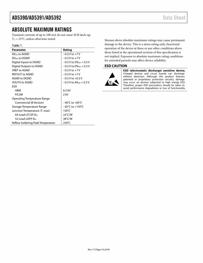
ABSOLUTE MAXIMUM RATINGS Transient currents of up to 100 mA do not cause SCR latch-up. TA = 25°C, unless otherwise noted.
Table 7. Parameter Rating AVDD to AGND −0.3 V to +7 V DVDD to DGND −0.3 V to +7 V Digital Inputs to DGND −0.3 V to DVDD + 0.3 V Digital Outputs to DGND −0.3 V to DVDD + 0.3 V VREF to AGND −0.3 V to +7 V REFOUT to AGND −0.3 V to +7 V AGND to DGND −0.3 V to +0.3 V VOUTX to AGND −0.3 V to AVDD + 0.3 V ESD
HBM 6.5 kV FICSM 2 kV
Operating Temperature Range Commercial (B Version) −40°C to +85°C
Storage Temperature Range −65°C to +150°C Junction Temperature (TJ max) 150°C
64-Lead LFCSP, θJA 22°C/W 52-Lead LQFP, θJA 38°C/W
Reflow Soldering Peak Temperature 230°C
Stresses above absolute maximum ratings may cause permanent damage to the device. This is a stress rating only; functional operation of the device at these or any other conditions above those listed in the operational sections of this specification is not implied. Exposure to absolute maximum rating conditions for extended periods may affect device reliability.
ESD CAUTION

Data Sheet AD5390/AD5391/AD5392
Rev. F | Page 15 of 44
PIN CONFIGURATONS AND FUNCTION DESCRIPTIONS
0377
3-00
8
PIN 1INDICATOR
DG
ND
SCLK
/SC
LSD
OD
V DD
DG
ND
DG
ND
54D
V DD
DG
ND
PD DC
EN/A
D1
LDA
C
55D
V DD
DIN
/SD
A
CLR
SPI/I
2 C
SYN
C/A
D0
64 63 62 61 60 59 58 57 56 53 52 51 50 49
33 VOUT 1334 VOUT 1435 VOUT 1536 AGND 237 AVDD 2
42 NC
46 RESET
41 NC40 NC39 NC38 NC
43 NC44 NC45 NC
47 BUSY48 NC1NC
2NC3NC4NC5NC6NC7REF_GND8REFOUT/REFIN9SIGNAL_GND 1
10DAC_GND 111AVDD 112VOUT 013141516
VOUT 1VOUT 2VOUT 3VOUT 4
TOP VIEW(Not to Scale)
AD5390/AD5391
AG
ND
1 1
7N
C 1
8N
C 1
9VO
UT
5 2
0VO
UT
6 2
1VO
UT
7 2
2M
ON
_IN
1 2
3M
ON
_IN
2 2
4M
ON
_OU
T 2
5VO
UT
8 2
6VO
UT
9 2
7VO
UT
10 2
8VO
UT
11 2
9VO
UT
12 3
0D
AC
_GN
D 2
31
SIG
NA
L_G
ND
2 3
2
NOTES1. NC = NO CONNECT.2. THE EXPOSED PAD SHOULD BE CONNECTED TO THE GROUND PLANE.
Figure 7. AD5390/AD5391 LFCSP Pin Configuration
0377
3-00
9
AD5392TOP VIEW
(Not to Scale)
PIN 1INDICATOR
AG
ND
1 1
7N
C 1
8N
C 1
9VO
UT
5 2
0VO
UT
6 2
1VO
UT
7 2
2M
ON
_IN
1 2
3M
ON
_IN
2 2
4M
ON
_OU
T 2
5TE
ST 2
6N
C 2
7N
C 2
8N
C 2
9N
C 3
0D
AC
_GN
D 2
31
SIG
NA
L_G
ND
2 3
2
DG
ND
SCLK
/SC
LSD
OD
V DD
DG
ND
DG
ND
54D
V DD
DG
ND
PD DC
EN/A
D1
LDA
C
55D
V DD
DIN
/SD
A
CLR
SPI/I
2 C
SYN
C/A
D0
64 63 62 61 60 59 58 57 56 53 52 51 50 49
33 NC34 NC35 NC36 NC37 NC
42 NC
46 RESET
41 NC40 NC39 NC38 NC
43 NC44 NC45 NC
47 BUSY48 NC1NC
2NC3NC4NC5NC6NC7REF_GND8REFOUT/REFIN9SIGNAL_GND 1
10DAC_GND 111AVDD 112VOUT 013141516
VOUT 1VOUT 2VOUT 3VOUT 4
NOTES1. NC = NO CONNECT.2. THE EXPOSED PAD SHOULD BE CONNECTED TO THE GROUND PLANE.
Figure 8. AD5392 LFCSP Pin Configuration
52 51 50 49 48 43 42 41 4047 46 45 44
14 15 16 17 18 19 20 21 22 23 24 25 26
1
2
3
4
5
6
7
8
9
10
11
13
12
39
38
37
36
35
34
33
32
31
30
29
28
27
AG
ND
1VO
UT
5VO
UT
6VO
UT
7M
ON
_IN
1M
ON
_IN
2M
ON
_OU
TVO
UT
8VO
UT
9VO
UT
10VO
UT
11VO
UT
12D
AC
_GN
D 2
CLRNCNC
REF_GNDREFOUT/REFINSIGNAL_GND 1
DAC_GND 1AVDD 1VOUT 0VOUT 1VOUT 2VOUT 3VOUT 4
LDACBUSYRESETNCNCNCNCAVDD 2AGND 2VOUT 15VOUT 14VOUT 13SIGNAL_GND 2
NC = NO CONNECT
DG
ND
DIN
/SD
ASC
LK/S
CL
SDO
DV D
DD
GN
DD
V DD
DV D
DD
GN
DSP
I/I2 C
PD DC
EN/A
D1
SYN
C/A
D0
PIN 1INDICATOR
AD5390/AD5391TOP VIEW
(Not to Scale)
0377
3-01
0
Figure 9. AD5390/AD5391 LQFP Pin Configuration
52 51 50 49 48 43 42 41 4047 46 45 44
14 15 16 17 18 19 20 21 22 23 24 25 26
1
2
3
4
5
6
7
8
9
10
11
13
12
39
38
37
36
35
34
33
32
31
30
29
28
27
AG
ND
1VO
UT
5VO
UT
6VO
UT
7M
ON
_IN
1M
ON
_IN
2M
ON
_OU
TTE
ST NC
NC
NC
NC
DA
C_G
ND
2
CLRNCNC
REF_GNDREFOUT/REFINSIGNAL_GND 1
DAC_GND 1AVDD 1VOUT 0VOUT 1VOUT 2VOUT 3VOUT 4
LDACBUSYRESETNCNCNCNCNCNCNCNCNCSIGNAL_GND 2
NC = NO CONNECT
DG
ND
DIN
/SD
ASC
LK/S
CL
SDO
DV D
DD
GN
DD
V DD
DV D
DD
GN
DSP
I/I2 C
PD DC
EN/A
D1
SYN
C/A
D0
PIN 1INDICATOR
AD5392TOP VIEW
(Not to Scale)
0377
3-01
1
Figure 10. AD5392 LQFP Pin Configuration

AD5390/AD5391/AD5392 Data Sheet
Rev. F | Page 16 of 44
Table 8. Pin Function Descriptions Mnemonic Function VOUT X Buffered Analog Outputs for Channel X. Each analog output is driven by a rail-to-rail output amplifier operating at a gain
of 2. Each output is capable of driving an output load of 5 kΩ to ground. Typical output impedance is 0.5 Ω. SIGNAL_GND 1, SIGNAL_GND 2
Analog Ground Reference Points for each group of eight output channels. All SIGNAL_GND pins are tied together internally and should be connected to the AGND plane as close as possible to the AD5390/AD5391/AD5392.
DAC_GND 1, DAC_GND 2
Each group of eight channels contains a DAC_GND pin. This is the ground reference point for the internal 14-bit DACs. These pins should be connected to the AGND plane.
AGND 1, AGND 2 Analog Ground Reference Point. Each group of eight channels contains an AGND pin. All AGND pins should be connected externally to the AGND plane.
AVDD 1, AVDD 2 Analog Supply Pins. Each group of eight channels has a separate AVDD pin. These pins should be decoupled with 0.1 uF ceramic capacitors and 10 µF tantalum capacitors. Operating range is 5 V ± 10%.
DGND Ground for All Digital Circuitry. DVDD Logic Power Supply. Guaranteed operating range is 2.7 V to 5.5 V. Recommended that these pins be decoupled with
0.1 µF ceramic capacitors and 10 µF tantalum capacitors to DGND. REF_GND Ground Reference Point for the Internal Reference. Connect to AGND. REFOUT/REFIN The AD5390/AD5391/AD5392 contains a common REFOUT/REFIN pin. When the internal reference is selected, this pin is
the reference output. If the application necessitates the use of an external reference, it can be applied to this pin and the internal reference disabled via the control register. The default for this pin is a reference input.
MON_OUT Analog Output Pin. When the monitor function is enabled on the AD5390/AD5391, the MON_OUT acts as the output of a 16-to-1 channel multiplexer that can be programmed to multiplex any channel output to the MON_OUT pin. When the monitor function is enabled on the AD5392, the MON_OUT acts as the output of an 8-to-1 channel multiplexer that can be programmed to multiplex any channel output to the MON_OUT pin. The MON_OUT pin output impedance is typically 500 Ω and is intended to drive a high input impedance such as that exhibited by SAR ADC inputs.
MON_IN 1, MON_IN 2
Monitor Input Pins. The AD5390/AD5391/AD5392 contains two monitor input pins to which the user can connect input signals (within the maximum ratings of the device) for monitoring purposes. Any of the signals applied to the MON_IN pins along with the output channels can be switched to the MON_OUT pin via software. An external ADC, for example, can be used to monitor these signals.
SYNC/AD0 Serial Interface Pin. This is the frame synchronization input signal for the serial interface. When taken low, the internal counter is enabled to count the required number of clocks before the addressed register is updated. In I2C mode, AD0 acts as a hardware address pin.
DCEN/AD1 Interface Control Pin. Operation is determined by the interface select bit SPI/I2C. Serial Interface Mode: Daisy-Chain Select Input (level-sensitive, active high). When high, this pin enables daisy-chain operation to allow a number of devices to be cascaded together. I2C Mode: This pin acts as a hardware address pin used in conjunction with AD0 to determine the software address for this device on the I2C bus.
SDO Serial Data Output. Three-state CMOS output. SDO can be used for daisy-chaining a number of devices together. Data is clocked out on SDO on the rising edge of SCLK and is valid on the falling edge of SCLK.
BUSY Digital CMOS Output. BUSY goes low during internal calculations of the data (x2) loaded to the DAC data register. During this time, the user can continue writing new data to further the x1, c, and m registers (these are stored in a FIFO), but no further updates to the DAC registers and DAC outputs can take place. If LDAC is taken low while BUSY is low, this event is stored. BUSY also goes low during power-on reset and when the RESET pin is low. During this time the interface is disabled and any events on LDAC are ignored. A CLR operation also brings BUSY low.
LDAC Load DAC Logic Input (active low). If LDAC is taken low while BUSY is inactive (high), the contents of the input registers are transferred to the DAC registers and the DAC outputs are updated. If LDAC is taken low while BUSY is active and internal calculations are taking place, the LDAC event is stored and the DAC registers are updated when BUSY goes inactive. However, any events on LDAC during power-on reset or RESET are ignored.
CLR Asynchronous Clear Input. The CLR input is falling edge sensitive. While CLR is low, all LDAC pulses are ignored. When CLR is activated, all channels are updated with the data contained in the CLR code register. BUSY is low for a duration of 20 µs (AD5390/AD5391) and 15 µs (AD5392) while all channels are being updated with the CLR code.
RESET Asynchronous Digital Reset Input (falling edge sensitive). The function of this pin is equivalent to that of the power-on reset generator. When this pin is taken low, the state machine initiates a reset sequence to digitally reset the x1, m, c, and x2 registers to their default power-on values. This sequence takes 270 µs maximum. This falling edge of RESET initiates the RESET process and BUSY goes low for the duration, returning high when RESET is complete. While BUSY is low, all interfaces are disabled and all LDAC pulses are ignored. When BUSY returns high, the part resumes normal operation and the status of the RESET pin is ignored until the next falling edge is detected.

Data Sheet AD5390/AD5391/AD5392
Rev. F | Page 17 of 44
Mnemonic Function PD Power-Down (level-sensitive, active high). Used to place the device in low power mode, in which the device consumes
1 µA analog current and 20 µA digital current. In power-down mode, all internal analog circuitry is placed in low power mode; the analog output is configured as high impedance outputs or provides a 100 kΩ load to ground, depending on how the power-down mode is configured. The serial interface remains active during power-down.
SPI/I2C Interface Select Input Pin. When this input is low, I2C mode is selected. When this input is high, SPI mode is selected.
SCLK/SCL Interface Clock Input Pin. In SPI-compatible serial interface mode, this pin acts as a serial clock input. It operates at clock speeds up to 50 MHz. I2C mode: In I2C mode, this pin performs the SCL function, clocking data into the device. Data transfer rate in I2C mode is compatible with both 100 kHz and 400 kHz operating modes.
DIN/SDA Interface Data Input Pin. SPI/I2C = 1: This pin acts as the serial data input. Data must be valid on the falling edge of SCLK. SPI/I2C = 0, I2C mode: In I2C mode, this pin is the serial data pin (SDA) operating as an open drain input/output.
TEST Test pin (AD5392 only). This pin is used for production testing. For normal operation, this pin should not be connected.
NC No Connect. These pins have no internal connection. Exposed Pad (LFCSP only)
This pad should be connected to the ground plane.

AD5390/AD5391/AD5392 Data Sheet
Rev. F | Page 18 of 44
TERMINOLOGY Relative Accuracy or Endpoint Linearity (INL) A measure of the maximum deviation from a straight line passing through the endpoints of the DAC transfer function. It is measured after adjusting for zero-scale error and full-scale error and is expressed in least significant bits (LSBs).
Differential Nonlinearity (DNL) The difference between the measured change and the ideal 1 LSB change between any two adjacent codes. A specified differential nonlinearity of 1 LSB maximum ensures mono-tonicity.
Zero-Scale Error The error in the DAC output voltage when all 0s are loaded into the DAC register. Ideally, with all 0s loaded to the DAC and m = all 1s, c = 2n−1, VOUT(Zero-Scale) = 0 V.
Zero-scale error is a measure of the difference between VOUT (actual) and VOUT (ideal) expressed in mV. It is mainly caused by offsets in the output amplifier.
Offset Error A measure of the difference between VOUT (actual) and VOUT (ideal) expressed in mV in the linear region of the transfer function. Offset error is measured on the AD5390-5/AD5391-5/ AD5392-5 with code 32 loaded in the DAC register and with code 64 loaded in the DAC register on the AD5390-3/AD5391-3/ AD5392-3.
Gain Error The deviation in slope of the DAC transfer characteristic from ideal and is expressed in % FSR with the DAC output unloaded. Gain error is specified in the linear region of the output range between VOUT = 10 mV and VOUT = AVDD − 50 mV.
DC Crosstalk The dc change in the output level of one DAC at midscale in response to a full-scale code (all 0s to all 1s and vice versa) and the output change of all other DACs. It is expressed in LSBs.
DC Output Impedance The effective output source resistance. It is dominated by package lead resistance.
Output Voltage Settling Time The amount of time it takes for the output of a DAC to settle to a specified level for a ¼ to ¾ full-scale input change. It is measured from the rising edge of BUSY.
Digital-to-Analog Glitch Energy The amount of energy injected into the analog output at the major code transition. It is specified as the area of the glitch in nV-s. It is measured by toggling the DAC register data between 0x1FFF and 0x2000.
DAC-to-DAC Crosstalk The glitch impulse that appears at the output of one DAC due to both the digital change and subsequent analog output change at another DAC. The victim channel is loaded with midscale, and DAC-to-DAC crosstalk is specified in nV-s.
Digital Crosstalk The glitch impulse transferred to the output of one converter due to a change in the DAC register code of another converter is defined as the digital crosstalk and is specified in nV-s.
Digital Feedthrough When the device is not selected, high frequency logic activity on the device’s digital inputs can be capacitively coupled both across and through the device to show up as noise on the VOUT pins. It can also be coupled along the supply and ground lines. This noise is digital feedthrough.
Output Noise Spectral Density This is a measure of internally generated random noise. Random noise is characterized as a spectral density (voltage per √Hz). It is measured by loading all DACs to midscale and measuring noise at the output. It is measured in nV/(Hz)1/2 in a 1 Hz bandwidth at 10 kHz.

Data Sheet AD5390/AD5391/AD5392
Rev. F | Page 19 of 44
TYPICAL PERFORMANCE CHARACTERISTICS
INPUT CODE163840 4096 8192 12288
INL
ERR
OR
(LSB
)
–2.0
2.0
1.5
1.0
0.5
0
–0.5
–1.0
–1.5
AVDD = DVDD = 5.5VVREF = 2.5VTA = 25°C
0377
3-04
0
Figure 11. AD5390-5/AD5392-5 Typical INL Plot 03
773-
041
INPUT CODE163840 4096 8192 12288
INL
ERR
OR
(LSB
)
–2.0
2.0
1.5
1.0
0.5
0
–0.5
–1.0
–1.5
AVDD = DVDD = 3VVREF = 1.25VTA = 25°C
Figure 12. AD5390-3/AD5392-3 INL Plot
0377
3-04
2
14
12
10
8
6
4
2
0–2 –1 0 1 2
AVDD = 5.5VREFIN = 2.5VTA = 25°C
NU
MB
ER O
F U
NIT
S
INL ERROR DISTRIBUTION (LSB)
Figure 13. AD5390/AD5392 INL Histogram Plot
0377
3-04
3
1.00
0.50
0.75
0.25
0
–0.25
–0.50
–0.75
–1.000 512 1024 1536 2048 2560 3072 3584 4096
INL
ERR
OR
(LSB
)
INPUT CODE
Figure 14. Typical AD5391-5 INL Plot
0377
3-04
4
1.00
0.50
0.75
0.25
0
–0.25
–0.50
–0.75
–1.000 512 1024 1536 2048 2560 3072 3584 4096
INL
ERR
OR
(LSB
)
INPUT CODE
Figure 15. Typical AD5391-3 INL Plot
0377
3-04
5
REFERENCE DRIFT (ppm/°C)
–5.0–1.5 2.5–3.5–4.5
–4.00.5–0.5 3.5–2.5 1.5
–1.0 3.0–3.0 1.00 4.0 5.04.5
–2.0 2.0
FREQ
UEN
CY
0
40
30
20
35
25
15
10
5
AVDD = 5VREFOUT = 2.5VTEMP. RANGE = 25°C TO 85°CSAMPLE SIZE = 162
Figure 16. AD5390/AD5391/AD5392 REFOUT Temperature Coefficient
AD5390/AD5391/AD5392 Data Sheet
Rev. F | Page 20 of 44
0377
3-10
0
BUSY
VOUT
AVDD = DVDD = 5VVREF = 2.5VTA = 25°C
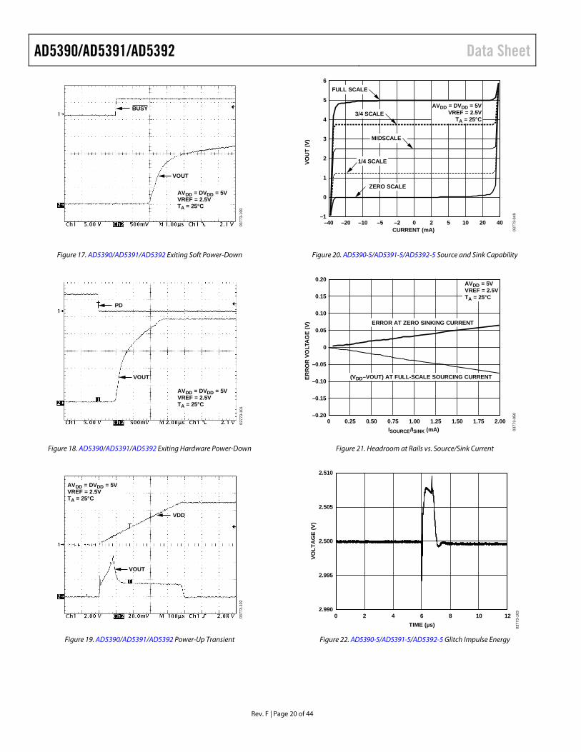
Figure 17. AD5390/AD5391/AD5392 Exiting Soft Power-Down
0377
3-10
1
PD
VOUT
AVDD = DVDD = 5VVREF = 2.5VTA = 25°C
Figure 18. AD5390/AD5391/AD5392 Exiting Hardware Power-Down
0377
3-10
2
VDD
VOUT
AVDD = DVDD = 5VVREF = 2.5VTA = 25°C
Figure 19. AD5390/AD5391/AD5392 Power-Up Transient
0377
3-04
9
CURRENT (mA)–40 –20 –10 –5 –2 0 2 5 10 20 40
VOU
T (V
)
–1
6
4
3
2
5
1
0
ZERO SCALE
1/4 SCALE
MIDSCALE
3/4 SCALE
FULL SCALE
AVDD = DVDD = 5VVREF = 2.5V
TA = 25°C
Figure 20. AD5390-5/AD5391-5/AD5392-5 Source and Sink Capability
0377
3-05
0
ISOURCE/ISINK (mA)2.000 0.25 0.50 0.75 1.00 1.25 1.50 1.75
ERR
OR
VO
LTA
GE
(V)
–0.20
0.20
0.10
0.05
0.15
0
–0.05
–0.10
–0.15
AVDD = 5VVREF = 2.5VTA = 25°C
ERROR AT ZERO SINKING CURRENT
(VDD–VOUT) AT FULL-SCALE SOURCING CURRENT
Figure 21. Headroom at Rails vs. Source/Sink Current
2.510
2.505
2.500
2.995
2.9900 12108642
VOLT
AG
E (V
)
TIME (µs) 0377
3-10
3
Figure 22. AD5390-5/AD5391-5/AD5392-5 Glitch Impulse Energy

Data Sheet AD5390/AD5391/AD5392
Rev. F | Page 21 of 44
0 12108642
VOLT
AG
E (V
)
TIME (µs) 0377
3-10
4
1.260
1.255
1.250
1.245
1.240
Figure 23. AD5390-3/AD5391-3/AD5392-3 Glitch Impulse
0377
3-10
5
LDAC
VOUT
AVDD = DVDD = 5VVREF = 2.5VTA = 25°C
Figure 24. AD5390/AD5391/AD5392 Slew Rate Boost Off
0377
3-10
6
LDAC
VOUT
AVDD = DVDD = 5VVREF = 2.5VTA = 25°C
Figure 25. AD5390/AD5391/AD5392 Slew Rate Boost On
0377
3-10
7
DIDD (mA)0.9 1.00.5 0.6 0.7 0.8
NU
MB
ER O
F U
NIT
S
0
10
8
6
4
2
DVDD = 5.5VVIH = DVDDVIL = DGNDTA = 25°C
Figure 26. AD5390/AD5391/AD5392 DIDD Histogram
0377
3-05
6
SAMPLE NUMBER5500 100 150 200 250 30050 350 400 500450
AM
PLIT
UD
E (V
)
2.449
2.456
2.455
2.454
2.453
2.452
2.451
2.450
AVDD = DVDD = 5VVREF = 2.5VTA = 25°C14ns/SAMPLE NUMBER
Figure 27. AD5390/AD5391/AD5392 Adjacent Channel Crosstalk
0377
3-05
7
FREQUENCY (Hz)100k100 1k 10k
OU
TPU
T N
OIS
E (n
V/ H
z)
0
600
500
400
300
200
100
AVDD = 5VTA = 25°CREFOUT DECOUPLEDWITH 100nF CAPACITOR
REFOUT = 2.5V
REFOUT = 1.25V
Figure 28. AD5390/AD5391/AD5392 REFOUT Noise Spectral Density

AD5390/AD5391/AD5392 Data Sheet
Rev. F | Page 22 of 44
0377
3-05
8
AVDD = DVDD = 5VTA = 25°CDAC LOADED WITH MIDSCALEEXTERNAL REFERENCEY AXIS = 5µV/DIVX AXIS = 100ms/DIV
Figure 29. 0.1 Hz to 10 Hz Output Noise Plot
0377
3-05
9
CURRENT (mA)–40 –20 –10 –5 –2 0 2 5 10 20 40
VOU
T (V
)
–1
6
4
3
2
5
1
0
ZERO SCALE 1/4 SCALE
MIDSCALE
3/4 SCALE
FULL SCALE
AVDD = DVDD = 3VVREF = 1.25VTA = 25°C
Figure 30. AD5390-3/AD5391-3/AD5392-3 Source and Sink Current Capability

Data Sheet AD5390/AD5391/AD5392
Rev. F | Page 23 of 44
FUNCTIONAL DESCRIPTION DAC ARCHITECTURE The AD5390/AD5391 are complete single-supply, 16-channel, voltage output DACs offering a resolution of 14 bits and 12 bits, respectively. The AD5392 is a complete single-supply, 8-channel, voltage output DAC offering 14-bit resolution. All devices are available in a 64-lead LFCSP and 52-lead LQFP, and feature serial interfaces. This family includes an internal select-able 1.25 V/2.5 V, 10 ppm/°C reference that can be used to drive the buffered reference inputs (alternatively, an external reference can be used to drive these inputs). All channels have an on-chip output amplifier with rail-to-rail output capable of driving a 5 kΩ load in parallel with a 200 pF capacitance.
The architecture of a single DAC channel consists of a 12-bit and 14-bit resistor-string DAC followed by an output buffer amplifier operating at a gain of 2. This resistor-string architecture guarantees DAC monotonicity. The 12-bit and 14-bit binary digital code loaded to the DAC register determines at what node on the string the voltage is tapped off before being fed to the output amplifier. Each channel on these devices contains independent offset and gain control registers, allowing the user to digitally trim offset and gain.
x1 INPUTREG
m REG
c REG
x2 DACREG
14-BITDAC
INPUTDATA
R
R
AVDD
VOUT
VREF
0377
3-01
8
Figure 31. Single-Channel Architecture
These registers let the user calibrate out errors in the complete signal chain including the DAC using the internal m and c registers, which hold the correction factors. All channels are double-buffered, allowing synchronous updating of all channels using the LDAC pin. Figure 31 shows a block diagram of a single channel on the AD5390/AD5391/AD5392.
The digital input transfer function for each DAC can be represented as
( )( ) ( )1212/22 −−+×+= nn cxmx
where: x2 is the data-word loaded to the resistor-string DAC. x1 is the 12-bit and 14-bit data-word written to the DAC input register. m is the 12-bit and 14-bit gain coefficient (default is all 0x3FFE on the AD5390/AD5392 and 0xFFE on the AD5391). The LSB of the gain coefficient is zero. n = DAC resolution (n = 14 for the AD5390/AD5392 and n = 12 for the AD5391). c is the 12-bit and 14-bit offset coefficient (default is 0x2000 on the AD5390/AD5392 and 0x800 on the AD5391).
The complete transfer function for these devices can be represented as
nxVREFVOUT 2/22 ××=
where: x2 is the data-word loaded to the resistor-string DAC. VREF is the reference voltage applied to the REFIN/REFOUT pin on the DAC when an external reference is used (2.5 V for specified performance on the AD5390-5/AD5391-5/AD5392-5 and 1.25 V on the AD5390-3/AD5391-3/AD5392-3).

AD5390/AD5391/AD5392 Data Sheet
Rev. F | Page 24 of 44
DATA DECODING AD5390/AD5392
The AD5390/AD5392 contain an internal 14-bit data bus. The input data is decoded depending on the data loaded to the REG1 and REG0 bits of the input serial register. This is shown in Table 9.
Data from the serial input register is loaded into the addressed DAC input register, offset (c) register, or gain (m) register. The format data, and the offset (c) and gain (m) register contents are shown in Table 10 to Table 12.
Table 9. Register Selection REG1 REG0 Register Selected
1 1 Input data register (x1) 1 0 Offset register (c) 0 1 Gain register (m) 0 0 Special function registers (SFRs)
Table 10. AD5390/AD5392 DAC Data Format (REG1 = 1, REG0 = 1) DB13 to DB0 DAC Output (V)
11 1111 1111 1111 2 VREF × (16383/16384) 11 1111 1111 1110 2 VREF × (16382/16384) 10 0000 0000 0001 2 VREF × (8193/16384) 10 0000 0000 0000 2 VREF × (8192/16384) 01 1111 1111 1111 2 VREF × (8191/16384) 00 0000 0000 0001 2 VREF × (1/16384) 00 0000 0000 0000 0
Table 11. AD5390/AD5392 Offset Data Format (REG1 = 1, REG0 = 0) DB13 to DB0 Offset (LSB)
111111 1111 1111 +8191 111111 1111 1110 +8190 100000 0000 0001 +1 100000 0000 0000 +0 011111 1111 1111 –1 000000 0000 0001 –8191 000000 0000 0000 –8192
Table 12. AD5390/AD5392 Gain Data Format (REG1 = 0, REG0 = 1) DB13 to DB0 Gain Factor
11 1111 1111 1110 1 10 1111 1111 1110 0.75 01 1111 1111 1110 0.5 00 1111 1111 1110 0.25 00 0000 0000 0000 0
AD5391
The AD5391 contains an internal 12-bit data bus. The input data is decoded depending on the value loaded to the REG1 and REG0 bits of the input serial register. The input data from the serial input register is loaded into the addressed DAC input register, offset (c) register, or gain (m) register. The format data and the offset (c) and gain (m) register contents are shown in Table 13 to Table 15.
Table 13. AD5391 DAC Data Format (REG1 = 1, REG0 = 1) DB11 to DB0 DAC Output (V)
1111 1111 1111 2 VREF × (4095/4096) 1111 1111 1110 2 VREF × (4094/4096) 1000 0000 0001 2 VREF × (2049/4096) 1000 0000 0000 2 VREF × (2048/4096) 0111 1111 1111 2 VREF × (2047/4096) 0000 0000 0001 2 VREF × (1/4096) 0000 0000 0000 0
Table 14. AD5391 Offset Data Format (REG1 = 1, REG0 = 0) DB11 to DB0 Offset (LSB)
1111 1111 1111 +2047 1111 1111 1110 +2046 1000 0000 0001 +1 1000 0000 0000 +0 0111 1111 1111 –1 0000 0000 0001 –2047 0000 0000 0000 –2048
Table 15. AD5391 Gain Data Format (REG1 = 0, REG0 = 1) DB11 to DB0 Gain Factor
1111 1111 1110 1 1011 1111 1110 0.75 0111 1111 1110 0.5 0011 1111 1110 0.25 0000 0000 0000 0

Data Sheet AD5390/AD5391/AD5392
Rev. F | Page 25 of 44
INTERFACES The AD5390/AD5391/AD5392 contain a serial interface that can be programmed to be DSP-, SPI-, and MICROWIRE-compatible, or I2C-compatible. The SPI/I2C pin is used to select the interface mode.
To minimize both the power consumption of the device and the on-chip digital noise, the interface fully powers up only when the device is being written to, that is, on the falling edge of SYNC.
DSP-, SPI-, AND MICROWIRE-COMPATIBLE SERIAL INTERFACE The serial interface can be operated with a minimum of three wires in standalone mode or four wires in daisy-chain mode. Daisy-chaining allows many devices to be cascaded together to increase system channel count. The SPI/I2C pin is tied to a
Logic 1 pin to configure this mode of operation. The serial interface control pins are described in Table 16.
Table 16. Serial Interface Control Pins Pin Description SYNC, DIN, SCLK Standard 3-wire interface pins.
DCEN Selects standalone mode or daisy-chain mode. SDO Data out pin for daisy-chain mode.
Figure 2 to Figure 4 show timing diagrams for a serial write to the AD5390/AD5391/AD5392 in both standalone and daisy-chain mode. The 24-bit data-word format for the serial interface is shown in Table 17 to Table 19. Descriptions of the bits follow in Table 20.
Table 17. AD5390 16-Channel, 14-Bit DAC Serial Input Register Configuration MSB LSB
A/B R/W 0 0 A3 A2 A1 A0 REG1 REG0 DB13 DB12 DB11 DB10 DB9 DB8 DB7 DB6 DB5 DB4 DB3 DB2 DB1 DB0
Table 18. AD5391 16-Channel, 12-Bit DAC Serial Input Register Configuration MSB LSB
A/B R/W 0 0 A3 A2 A1 A0 REG1 REG0 DB11 DB10 DB9 DB8 DB7 DB6 DB5 DB4 DB3 DB2 DB1 DB0 X X
Table 19. AD5392 8-Channel, 14-Bit DAC Serial Input Register Configuration MSB LSB
A/B R/W 0 0 0 A2 A1 A0 REG1 REG0 DB13 DB12 DB11 DB10 DB9 DB8 DB7 DB6 DB5 DB4 DB3 DB2 DB1 DB0
Table 20. Serial Input Register Configuration Bit Descriptions Bit Description A/B When toggle mode is enabled, this bit selects whether the data write is to the A or B register. With toggle mode disabled, this
bit should be set to zero to select the A data register. R/W The read or write control bit.
A3 to A0 Used to address the input channels. REG1 and REG0
Select the register to which data is written, as outlined in Table 9.
DB13 to DB0
Contain the input data-word.
X Don’t care condition.

AD5390/AD5391/AD5392 Data Sheet
Rev. F | Page 26 of 44
Standalone Mode
By connecting the daisy-chain enable (DCEN) pin low, stand-alone mode is enabled. The serial interface works with both a continuous and a noncontinuous serial clock. The first falling edge of SYNC starts the write cycle and resets a counter that counts the number of serial clocks to ensure that the correct number of bits is shifted into the serial shift register. Any further edges on SYNC (except for a falling edge) are ignored until 24 bits are clocked in. Once 24 bits have been shifted in, the SCLK is ignored. For another serial transfer to take place, the counter must be reset by the falling edge of SYNC.
Daisy-Chain Mode
For systems that contain several devices, the SDO pin can be used to daisy-chain the devices together. This daisy-chain mode can be useful in system diagnostics and for reducing the number of serial interface lines.
By connecting the DCEN pin high, daisy-chain mode is enabled. The first falling edge of SYNC starts the write cycle. The SCLK is continuously applied to the input shift register when SYNC is low. If more than 24 clock pulses are applied, the data ripples out of the shift register and appears on the SDO line. This data is clocked out on the rising edge of SCLK and is valid on the falling edge. By connecting the SDO of the first device to the DIN input on the next device in the chain, a multidevice interface is constructed. For each device in the system, 24 clock pulses are required. Therefore, the total number of clock cycles must equal 24N where N is the total number of AD5390/AD5391/AD5392 devices in the chain.
When the serial transfer to all devices is complete, SYNC is taken high. This latches the input data in each device in the daisy chain and prevents any further data from being clocked into the input shift register.
If SYNC is taken high before 24 clocks are clocked into the part, it is considered a bad frame and the data is discarded.
The serial clock can be either a continuous or a gated clock. A continuous SCLK source can be used only if the SYNC can be held low for the correct number of clock cycles. In gated clock mode, a burst clock containing the exact number of clock cycles must be used and SYNC taken high after the final clock to latch the data.
Readback Mode
Readback mode is invoked by setting the R/W bit = 1 in the serial input register write sequence. With R/W = 1, Bit A3 to Bit A0 in association with Bits REG1 and REG0 select the register to be read. The remaining data bits in the write sequence are don’t care bits. During the next SPI write, the data appearing on the SDO output contains the data from the previously addressed register. For a read of a single register, the NOP command can be used in clocking out the data from the selected register on SDO.
The readback diagram in Figure 32 shows the readback sequence. For example, to read back the m register of Channel 0 on the AD5390/AD5391/AD5392, the following sequence should be implemented:
First, write 0x404XXX to the AD5390/AD5391/AD5392 input register. This configures the AD5390/AD5391/AD5392 for read mode with the m register of Channel 0 selected. Note that all data bits, DB13 to DB0, are don’t care bits.
Follow this with a second write, a NOP condition, and 0x000000. During this write, the data from the m register is clocked out on the DOUT line, that is, data clocked out contains the data from the m register in Bit DB13 to Bit DB0, and the top 10 bits con-tain the address information as previously written. In readback mode, the SYNC signal must frame the data. Data is clocked out on the rising edge of SCLK and is valid on the falling edge of the SCLK signal. If the SCLK idles high between the write and read operations of a readback, the first bit of data is clocked out on the falling edge of SYNC.
24 48SCLK
SYNC
DIN
SDO
UNDEFINED SELECTED REGISTER DATA CLOCKED OUT
NOP CONDITIONINPUT WORD SPECIFIES REGISTER TO BE READ
DB23 DB0 DB0DB23
DB23 DB0 DB0DB23
0377
3-02
2
Figure 32. Readback Operation

Data Sheet AD5390/AD5391/AD5392
Rev. F | Page 27 of 44
I2C SERIAL INTERFACE The AD5390/AD5391/AD5392 feature an I2C-compatible 2-wire interface consisting of a serial data line (SDA) and a serial clock line (SCL). SDA and SCL facilitate communication between the DACs and the master at rates up to 400 kHz. Figure 6 shows the 2-wire interface timing diagram.
When selecting the I2C operating mode by configuring the SPI/I2C pin to Logic 0, the device is connected to the I2C bus as a slave device, that is, no clock is generated by the device. The AD5390/AD5391/AD5392 have a 7-bit slave address 1010 1 (AD1)(AD0). The five MSBs are hard-coded and the two LSBs are determined by the state of the AD1 and AD0 pins. The hardware configuration facility for the AD1 and AD0 pins allows four of these devices to be configured on the bus.
I2C Data Transfer
One data bit is transferred during each SCL clock cycle. The data on SDA must remain stable during the high period of the SCL clock pulse. Changes in SDA while SCL is high are control signals that configure START and STOP conditions. Both SDA and SCL are pulled high by the external pull-up resistors when the I2C bus is not busy.
START and STOP Conditions
A master device initiates communication by issuing a START condition. A START condition is a high-to-low transition on SDA with SCL high. A STOP condition is a low-to-high trans-ition on SDA, while SCL is high. A START condition from the master signals the beginning of a transmission to the AD5390/AD5391/AD5392. The STOP condition frees the bus. If a repeated START condition (Sr) is generated instead of a STOP condition, the bus remains active.
Repeated START Condition
A repeated START (Sr) condition may indicate a change of data direction on the bus. Sr may be used when the bus master is writing to several I2C devices and does not want to relinquish control of the bus.
Acknowledge Bit (ACK)
The acknowledge bit (ACK) is the ninth bit attached to any 8-bit data-word. An ACK is always generated by the receiving device. The AD5390/AD5391/AD5392 devices generate an ACK when receiving an address or data by pulling SDA low during the ninth clock period.
Monitoring the ACK allows for detection of unsuccessful data transfers. An unsuccessful data transfer occurs if a receiving device is busy or if a system fault has occurred. In the event of an unsuccessful data transfer, the bus master should reattempt communication.
AD5390/AD5391/AD5392 Slave Addresses
A bus master initiates communication with a slave device by issuing a START condition followed by the 7-bit slave address. When idle, the AD5390/AD5391/AD5392 device waits for a START condition followed by its slave address. The LSB of the address word is the read/write (R/W) bit. The AD5390/ AD5391/AD5392 devices are receive devices only and R/W = 0 when communicating with them. After receiving the proper address 1010 1(AD1) (AD0), the AD5390/AD5391/AD5392 issues an ACK by pulling SDA low for one clock cycle. The AD5390/AD5391/AD5392 has four user-programmable addresses determined by the AD1 and AD0 bits.

AD5390/AD5391/AD5392 Data Sheet
Rev. F | Page 28 of 44
I2C WRITE OPERATION There are three specific modes in which data can be written to the AD5390/AD5391/AD5392 DACs.
4-BYTE MODE When writing to the AD5390/AD5391/AD5392 DACs, begin with an address byte (R/W = 0), after which the DAC acknowledges that it is prepared to receive data by pulling SDA low. The address byte is followed by the pointer byte. This addresses the specific channel in the DAC to be addressed and
is also acknowledged by the DAC. Address Bits A3 to A0 address all channels on the AD5390/AD5391. Address Bits A2 to A0 address all channels on the AD5392. Address Bit A3 is a zero on the AD5392. Two bytes of data are then written to the DAC, as shown in Figure 33. A STOP condition follows. This lets the user update a single channel within the AD5390/ AD5391/AD5392 at any time and requires four bytes of data to be transferred from the master.
REG0 DB13 DB12 DB11 DB10 DB8DB9 DB7 DB6 DB5 DB4 DB3 DB2 DB1 DB0REG1
1 0 0 0 0 0 A3 A2 A1 A01 1 AD1 AD0 R/W
SCL
SDA
SCL
SDA
STARTCONDITION
BYMASTER
ACKBY
CONVERTER
ACKBY
CONVERTERADDRESS BYTE POINTER BYTE
MSB
ACKBY
CONVERTER
ACKBY
CONVERTER
STOPCONDITION
BYMASTER
MOST SIGNIFICANT DATA BYTE LEAST SIGNIFICANT DATA BYTE
A/B
0377
3-02
3
Figure 33. AD5390/AD5392 4-Byte Mode I2C Write Operation
REG0 DB11 DB10 DB9 DB8 DB6DB7 DB5 DB4 DB3 DB2 DB1 DB0 0 0REG1
1 0 0 0 0 0 A3 A2 A1 A01 1 AD1 AD0 R/W
SCL
SDA
SCL
SDA
STARTCONDITION
BYMASTER
ACKBY
CONVERTER
ACKBY
CONVERTERADDRESS BYTE POINTER BYTE
MSB
ACKBY
CONVERTER
ACKBY
CONVERTER
STOPCONDITION
BYMASTER
MOST SIGNIFICANT DATA BYTE LEAST SIGNIFICANT DATA BYTE
A/B
0377
3-02
1
Figure 34. AD5391 4-Byte Mode I2C Write Operation

Data Sheet AD5390/AD5391/AD5392
Rev. F | Page 29 of 44
3-BYTE MODE The 3-byte mode lets the user update more than one channel in a write sequence without having to write the device address byte each time. The device address byte is required only once and subsequent channel updates require the pointer byte and the data bytes. In 3-byte mode, the user begins with an address byte (R/W = 0) after which the DAC acknowledges that it is prepared to receive data by pulling SDA low. The address byte is followed by the pointer byte; this addresses the specific channel in the DAC to be addressed and is also acknowledged by the DAC. Address Bits A3 to A0 address all channels on the AD5390/ AD5391. Address Bits A2 to A0 address all channels on the
AD5392. Address Bit A3 is a zero on the AD5392. This is then followed by the two data bytes. REG1 and REG0 determine the register to be updated.
If a STOP condition is not sent following the data bytes, another channel can be updated by sending a new pointer byte followed by the data bytes. This mode requires only three bytes to be sent to update any channel once the device has been initially addressed and reduces the software overhead in updating the AD5390/AD5391/AD5392 channels. A STOP condition at any time exits this mode. Figure 35 shows a typical configuration.
REG0 MSB MSBLSB LSBREG1
ACKBY
CONVERTER
ACKBY
CONVERTER
STOPCONDITION
BYMASTER
REG0 MSB MSBLSB LSBREG1
1 0 0 0 0 0 A3 A2 A1 A01 1 AD1 AD0 R/W
SCL
SDA
SCL
SDA
SCL
SDA
SCL
SDA
STARTCONDITION
BYMASTER
ACKBY
CONVERTER
ACKBY
CONVERTERADDRESS BYTE POINTER BYTE FOR CHANNEL N
MSB
ACKBY
CONVERTER
ACKBY
CONVERTER
ACKBY
CONVERTER
MOST SIGNIFICANT DATA BYTE
MOST SIGNIFICANT DATA BYTE
POINTER BYTE FOR CHANNEL NEXT CHANNEL
DATA FOR CHANNEL N
DATA FOR CHANNEL NEXT CHANNEL
LEAST SIGNIFICANT DATA BYTE
LEAST SIGNIFICANT DATA BYTE
A/B
0 0 0 0 A3 A2 A1 A0
MSB
0377
3-02
4
Figure 35. 3-Byte Mode I2C Write Operation

AD5390/AD5391/AD5392 Data Sheet
Rev. F | Page 30 of 44
2-BYTE MODE The 2-byte mode lets the user update channels sequentially following initialization of this mode. The device address byte is required only once and the address pointer is configured for autoincrement or burst mode.
The user must begin with an address byte (R/W = 0), after which the DAC acknowledges that it is prepared to receive data by pulling SDA low. The address byte is followed by a specific pointer byte (0xFF), which initiates the burst mode of opera-tion. The address pointer initializes to Channel 0 and the data following the pointer is loaded to Channel 0. The address pointer automatically increments to the next address.
The REG0 and REG1 bits in the data byte determine the register to be updated. In this mode, following the initialization, only the two data bytes are required to update a channel. The channel address automatically increments from Address 0 to the final address and then returns to the normal 3-byte mode of operation. This mode allows transmission of data to all channels in one block and reduces the software overhead in configuring all channels. A STOP condition at any time exits this mode. Toggle mode of operation is not supported in 2-byte mode. Figure 36 shows a typical configuration.
REG0 MSB MSBLSB LSBREG1
1 0 0 A7 = 1 A6 = 1 A5 = 1 A4 = 1 A3 = 1 A2 = 1 A1 = 1 A0 = 11 1 AD1 AD0 R/W
SCL
SDA
SCL
SDA
SCL
SDA
SCL
SDA
STARTCONDITION
BYMASTER
ACKBY
CONVERTER
ACKBY
CONVERTERADDRESS BYTE POINTER BYTE
CHANNEL 1 DATA
CHANNEL 0 DATA
CHANNEL N DATA FOLLOWED BY STOP
MSB
ACKBY
CONVERTER
ACKBY
CONVERTER
MOST SIGNIFICANT DATA BYTE LEAST SIGNIFICANT DATA BYTE
REG0 MSB MSBLSB LSBREG1
ACKBY
CONVERTER
ACKBY
CONVERTERMOST SIGNIFICANT DATA BYTE LEAST SIGNIFICANT DATA BYTE
REG0 MSB MSBLSB LSBREG1
ACKBY
CONVERTER
ACKBY
CONVERTER
STOPCONDITION
BYMASTER
MOST SIGNIFICANT DATA BYTE LEAST SIGNIFICANT DATA BYTE
0377
3-02
5
Figure 36. 2-Byte Mode I2C Write Operation

Data Sheet AD5390/AD5391/AD5392
Rev. F | Page 31 of 44
AD5390/AD5391/AD5392 ON-CHIP SPECIAL FUNCTION REGISTERS The AD5390/AD5391/AD5392 contain a number of special function registers (SFRs) as shown in Table 21. SFRs are addressed with REG1 = 0 and REG0 = 0 and are decoded using Address Bit A3 to Bit A0.
Table 21. SFR Register Functions (REG1 = 0, REG0 = 0) R/ W A3 A2 A1 A0 Function
X 0 0 0 0 NOP (no operation) 0 0 0 0 1 Write CLR code 0 0 0 1 0 Soft CLR 0 1 0 0 0 Soft power-down 0 1 0 0 1 Soft power-up 0 1 1 0 0 Control register write 1 1 1 0 0 Control register read 0 1 0 1 0 Monitor channel 0 1 1 1 1 Soft reset SFR Commands
NOP (No Operation) REG1 = REG0 = 0, A3 to A0 = 0000
Performs no operation, but is useful in readback mode to clock out data on SDO for diagnostic purposes. BUSY outputs a low during a NOP operation.
Write CLR Code REG1 = REG0 = 0, A3 to A0 = 0001 DB13 to DB0 = Contain the CLR data
Bringing the CLR line low or exercising the soft clear function loads the contents of the DAC registers with the data contained in the user-configurable CLR register and sets VOUT 0 to VOUT 15, accordingly. This can be very useful not only for setting up a specific output voltage in a clear condition but for calibration purposes. For calibration, the user can load full scale or zero scale to the clear code register and then issue a hardware or software clear to load this code to all DACs, removing the need for individual writes to all DACs. Default on power-up is all zeros.
Soft CLR REG1 = REG0 = 0, A3 to A0 = 0010 DB13 to DB0 = Don’t Care
Executing this instruction performs the CLR, which is functionally the same as that provided by the external CLR pin. The DAC outputs are loaded with the data in the CLR code register. The time taken to execute fully the SOFT CLR is 20 µs on the AD5390/AD5391 and 15 µs on the AD5392. It is indicated by the BUSY low time.
Soft Power-Down REG1 = REG0 = 0, A3 to A0 = 1000 DB13 to DB0 = Don’t Care
Executing this instruction performs a global power-down, which puts all channels into a low power mode, reducing analog current to 1 µA maximum and digital power consumption to 20 µA maximum. In power-down mode, the output amplifier can be configured as a high impedance output or can provide a 100 kΩ load to ground. The contents of all internal registers are retained in power-down mode.
Soft Power-Up REG1 = REG0 = 0, A3 to A0 =1001 DB13 to DB0 = Don’t Care
This instruction is used to power up the output amplifiers and the internal references. The time to exit power-down mode is 8 µs. The hardware power-down and software functions are internally combined in a digital OR function.
Soft Reset REG1 = REG0 = 0, A5 to A0 = 001111 DB13 to DB0 = Don’t Care
This instruction is used to implement a software reset. All internal registers are reset to their default values, which correspond to m at full scale and c at zero scale. The contents of the DAC registers are cleared, setting all analog outputs to 0 V. The soft reset activation time is 135 µs maximum. Only perform a soft reset when the AD5390/AD5391/AD5392 is not in power-down mode.
Monitor Channel REG1 = REG0 = 0, A3 to A0 = 01010 DB13 to DB8 = Contain data to address the channel to be monitored
A monitor function is provided on all devices. This feature, consisting of a multiplexer addressed via the interface, allows any channel output to be routed to the MON_OUT pin for monitoring using an external ADC. In addition to monitoring all output channels, two external inputs are also provided, allowing the user to monitor signals external to the AD5390/ AD5391/AD5392. The channel monitor function must be enabled in the control register before any channels are routed to the MON_OUT pin. On the AD5390 and AD5392 14-bit parts, DB13 to DB8 contain the channel address for the monitored channel. On the AD5391 12-bit part, DB11 to DB6 contain the channel address for the channel to be monitored. Selecting Address 63 three-states the MON_OUT pin.
The channel monitor decoding for the AD5390/AD5392 is shown in Table 22 and the monitor decoding for the AD5391 is shown in Table 23.

AD5390/AD5391/AD5392 Data Sheet
Rev. F | Page 32 of 44
Table 22. AD5390/AD5392 Channel Monitor Decoding
REG1 REG0 A3 A2 A1 A0 DB13 DB12 DB11 DB10 DB9 DB8 DB7 to DB0 MON_OUT (AD5390)
MON_OUT (AD5392)
0 0 1 0 1 0 0 0 0 0 0 0 X VOUT 0 VOUT 0 0 0 1 0 1 0 0 0 0 0 0 1 X VOUT 1 VOUT 1 0 0 1 0 1 0 0 0 0 0 1 0 X VOUT 2 VOUT 2 0 0 1 0 1 0 0 0 0 0 1 1 X VOUT 3 VOUT 3 0 0 1 0 1 0 0 0 0 1 0 0 X VOUT 4 VOUT 4 0 0 1 0 1 0 0 0 0 1 0 1 X VOUT 5 VOUT 5 0 0 1 0 1 0 0 0 0 1 1 0 X VOUT 6 VOUT 6 0 0 1 0 1 0 0 0 0 1 1 1 X VOUT 7 VOUT 7 0 0 1 0 1 0 0 0 1 0 0 0 X VOUT 8 0 0 1 0 1 0 0 0 1 0 0 1 X VOUT 9 0 0 1 0 1 0 0 0 1 0 1 0 X VOUT 10 0 0 1 0 1 0 0 0 1 0 1 1 X VOUT 11 0 0 1 0 1 0 0 0 1 1 0 0 X VOUT 12 0 0 1 0 1 0 0 0 1 1 0 1 X VOUT 13 0 0 1 0 1 0 0 0 1 1 1 0 X VOUT 14 0 0 1 0 1 0 0 0 1 1 1 1 X VOUT 15 0 0 1 0 1 0 1 0 0 1 0 0 X MON_IN 1 MON_IN 1 0 0 1 0 1 0 1 0 0 1 0 1 X MON_IN 2 MON_IN 2 0 0 1 0 1 0 1 1 1 1 1 1 X Three-state Three-state
Table 23. AD5391 Channel Monitor Decoding REG1 REG0 A3 A2 A1 A0 DB11 DB10 DB9 DB8 DB7 DB6 DB5 to DB0 MON_OUT (AD5391)
0 0 1 0 1 0 0 0 0 0 0 0 X VOUT 0 0 0 1 0 1 0 0 0 0 0 0 1 X VOUT 1 0 0 1 0 1 0 0 0 0 0 1 0 X VOUT 2 0 0 1 0 1 0 0 0 0 0 1 1 X VOUT 3 0 0 1 0 1 0 0 0 0 1 0 0 X VOUT 4 0 0 1 0 1 0 0 0 0 1 0 1 X VOUT 5 0 0 1 0 1 0 0 0 0 1 1 0 X VOUT 6 0 0 1 0 1 0 0 0 0 1 1 1 X VOUT 7 0 0 1 0 1 0 0 0 1 0 0 0 X VOUT 8 0 0 1 0 1 0 0 0 1 0 0 1 X VOUT 9 0 0 1 0 1 0 0 0 1 0 1 0 X VOUT 10 0 0 1 0 1 0 0 0 1 0 1 1 X VOUT 11 0 0 1 0 1 0 0 0 1 1 0 0 X VOUT 12 0 0 1 0 1 0 0 0 1 1 0 1 X VOUT 13 0 0 1 0 1 0 0 0 1 1 1 0 X VOUT 14 0 0 1 0 1 0 0 0 1 1 1 1 X VOUT 15 0 0 1 0 1 0 1 0 0 1 0 0 X MON_IN 1 0 0 1 0 1 0 1 0 0 1 0 1 X MON_IN 2 0 0 1 0 1 0 1 1 0 1 1 0 X Undefined 0 0 1 0 1 0 1 1 . . . . X Undefined 0 0 1 0 1 0 1 1 1 1 1 0 X Undefined 0 0 1 0 1 0 1 1 1 1 1 1 X Three-state

Data Sheet AD5390/AD5391/AD5392
Rev. F | Page 33 of 44
CONTROL REGISTER WRITE Table 24 shows the control register contents for the AD5390 and the AD5392. Table 25 provides bit descriptions. Note that REG1 = REG0 = 0, A3 to A0 = 1100, and DB13 to DB0 contain the control register data.
Table 24. AD5390/AD5392 Control Register Contents MSB LSB CR13 CR12 CR11 CR10 CR9 CR8 CR7 CR6 CR5 CR4 CR3 CR2 CR1 CR0
Table 25. AD5390 and AD5392 Bit Descriptions Bit Description CR13 Power-Down Status. This bit is used to configure the output amplifier state in power–down mode.
CR13 = 1: Amplifier output is high impedance (default on power-up). CR13 = 0: Amplifier output is 100 kΩ to ground.
CR12 REF Select. This bit selects the operating internal reference for the AD5390/AD5391/AD5392. CR12 is programmed as follows: CR12 = 1: Internal reference is 2.5 V (AD5390-5/AD5392-5 default). Recommended operating reference for AD5390-5/ AD5391-5/AD5392-5. CR12 = 0: Internal reference is 1.25 V (AD5390-3/AD5392-3 default). Recommended operating reference for AD5390-3 and AD5392-3.
CR11 Current Boost Control. This bit is used to boost the current in the output amplifier, thus altering its slew rate and is configured as follows: CR11 = 1: Boost mode on. This maximizes the bias current in the output amplifier, optimizing its slew rate but increasing the power dissipation. CR11 = 0: Boost mode off (default on power-up). This reduces the bias current in the output amplifier and reduces the overall power consumption.
CR10 Internal/External Reference. This bit determines if the DAC uses its internal reference or an external reference. CR10 = 1: Internal reference enabled. Reference output depends on data loaded to CR12. CR10 = 0: External reference selected (default on power-up).
CR9 Channel Monitor Enable (see Table 22). CR9 = 1: Monitor enabled (default on power-up). This enables the channel monitor function. Following a write to the monitor channel in the SFR register, the selected channel output is routed to the MON_OUT pin. CR9 = 0: Monitor disabled. When monitor is disabled, the MON_OUT pin is three-stated.
CR8 Thermal Monitor Function. When enabled, this function is used to monitor the internal die temperature of the AD5390/AD5392. The thermal monitor powers down the output amplifiers when the temperature exceeds 130°C. This function can be used to protect the device when the power dissipation of the device may be exceeded, if a number of output channels are simultaneously short circuited. A soft power-up re-enables the output amplifiers if the die temperature has dropped below 130°C. CR8 = 1: Thermal monitor enabled. CR8 = 0: Thermal monitor disabled (default on power-up).
CR7 to CR4 Don’t Care. CR3 to CR2 Toggle Function Enable. This function lets the user toggle the output between two codes loaded to the A and B register
for each DAC. Control Register Bits CR3 and CR2 are used to enable individual groups of eight channels for operation in toggle mode on the AD5390 and AD5392, as follows: CR3 Group 1 Channel 8 to Channel 15 CR2 Group 0 Channel 0 to Channel 7 CR2 is the only active bit on the AD5392. Logic 1 written to any bit enables a group of channels and Logic 0 disables a group. LDAC is used to toggle between the two registers.
CR1 to CR0 Don’t Care.

AD5390/AD5391/AD5392 Data Sheet
Rev. F | Page 34 of 44
Table 26 shows the control register contents of the AD5391. Table 27 provides bit descriptions. Note that REG1 = REG0 = 0, A3 to A0 = 1100, and DB13 to DB0 contain the control register data.
Table 26. AD5391 Control Register Contents MSB LSB
CR11 CR10 CR9 CR8 CR7 CR6 CR5 CR4 CR3 CR2 CR1 CR0
Table 27. AD5391 Bit Descriptions Bit Description CR11 Power-Down Status. This bit is used to configure the output amplifier state in power-down mode.
CR11 = 1: Amplifier output is high impedance (default on power-up). CR11 = 0: Amplifier output is 100 kΩ to ground.
CR10 REF Select. This bit selects the operating internal reference for the AD5391. CR10 is programmed as follows: CR10 = 1: Internal reference is 2.5 V (AD5391-5 default). Recommended operating reference for AD5391-5. CR10 = 0: Internal reference is 1.25 V (AD5391-3 default). Recommended operating reference for AD5391-3.
CR9 Current Boost Control. This bit is used to boost the current in the output amplifier, thus altering its slew rate. This bit is configured as follows: CR9 = 1: Boost mode on. This maximizes the bias current in the output amplifier, optimizing its slew rate but increasing the power dissipation. CR9 = 0: Boost mode off (default on power-up). This reduces the bias current in the output amplifier and reduces the overall power consumption.
CR8 Internal/External Reference. This bits determines if the DAC uses its internal reference or an external reference. CR8 = 1: Internal reference enabled. Reference output depends on data loaded to CR10. CR8 = 0: External reference selected (default on power-up).
CR7 Channel Monitor Enable (see Table 23). CR7 = 1: Monitor enabled. This enables the channel monitor function. Following a write to the monitor channel in the SFR register, the selected channel output is routed to the MON_OUT pin. CR7 = 0: Monitor disabled (default on power-up). When monitor is disabled, the MON_OUT pin is three-stated.
CR6 Thermal Monitor Function. When enabled, this function is used to monitor the internal die temperature of the AD5391, when enabled. The thermal monitor powers down the output amplifiers when the temperature exceeds 130°C. This function can be used to protect the device in cases where the power dissipation of the device may be exceeded, if a number of output channels are simultaneously short circuited. A soft power-up re-enables the output amplifiers if the die temperature has dropped below 130°C. CR6 = 1: Thermal monitor enabled. CR6 = 0: Thermal monitor disabled (default on power-up).
CR5 to CR2 Don’t Care. CR1 to CR0 Toggle Function Enable. This function lets the user toggle the output between two codes loaded to the A and B register for
each DAC. Control Register Bit CR1 and Bit CR0 are used to enable individual groups of eight channels for operation in toggle mode on the AD5391, as follows: CR1 Group 1 Channel 8 to Channel 15 CR0 Group 0 Channel 0 to Channel 7 Logic 1 written to any bit enables a group of channels and Logic 0 disables a group. LDAC is used to toggle between the two registers.

Data Sheet AD5390/AD5391/AD5392
Rev. F | Page 35 of 44
HARDWARE FUNCTIONS RESET FUNCTION Bringing the RESET line low resets the contents of all internal registers to their power-on reset state. RESET is a negative edge- sensitive input. The default corresponds to m at full scale and c at zero scale. The contents of all DAC registers are cleared by setting the outputs to 0 V. This sequence takes 270 μs maximum. The falling edge of RESET initiates the reset process. BUSY goes low for the duration, returning high when RESET is complete. While BUSY is low, all interfaces are disabled and all LDAC pulses are ignored. When BUSY returns high, the part resumes normal operation, and the status of the RESET pin is ignored until the next falling edge is detected. Only perform a hardware reset when the AD5390/AD5391/AD5392 is not in power-down mode.
ASYNCHRONOUS CLEAR FUNCTION
CLR is negative-edge-triggered and BUSY goes low for the duration of the CLR execution. Bringing the CLR line low clears the contents of the DAC registers to the data contained in the user-configurable CLR register and sets the analog outputs accordingly. This function can be used in system calibration to load zero scale and full scale to all channels together. The execution time for a CLR is 20 μs on the AD5390/AD5391 and 15 μs on the AD5392.
BUSY AND LDAC FUNCTIONS
BUSY is a digital CMOS output indicating the status of the AD5390/AD5391/AD5392 devices. BUSY goes low during internal calculations of x2 data. If LDAC is taken low while BUSY is low, this event is stored. The user can hold the LDAC input permanently low and, in this case, the DAC outputs update immediately after BUSY goes high. BUSY also goes low during a power-on reset and when a falling edge is detected on the RESET pin. During this time, all interfaces are disabled and any events on LDAC are ignored.
The AD5390/AD5391/AD5392 contain an extra feature whereby a DAC register is not updated unless its x2 register has been written to since the last time LDAC was brought low. Normally, when LDAC is brought low, the DAC registers are filled with the contents of the x2 registers. However, these devices update the DAC register only if the x2 data has changed, thereby removing unnecessary digital crosstalk.
POWER-ON RESET The AD5390/AD5391/AD5392 contain a power-on reset generator and state machine. The power-on reset resets all registers to a predefined state, and the analog outputs are configured as high impedance outputs. The BUSY pin goes low during the power-on reset sequence, preventing data writes to the device.
POWER-DOWN The AD5390/AD5391/AD5392 contain a global power-down feature that puts all channels into a low power mode, reducing the analog power consumption to 1 μA maximum and the digital power consumption to 20 μA maximum. In power-down mode, the output amplifier can be configured as a high impedance output or to provide a 100 kΩ load to ground. The contents of all internal registers are retained in power-down mode. When exiting power-down, the settling time of the amplifier elapses before the outputs settle to their correct value.
MICROPROCESSOR INTERFACING AD5390/AD5391/AD5392 to MC68HC11
The serial peripheral interface (SPI) on the MC68HC11 is configured for master mode (MSTR = 1), clock polarity bit (CPOL) = 0, and the clock phase bit (CPHA) = 1. The SPI is configured by writing to the SPI control register (SPCR)—see the 68HC11 User Manual. SCK of the MC68HC11 drives the SCLK of the AD5390/AD5391/AD5392, the MOSI output drives the serial data line (DIN) of the AD5390/AD5391/ AD5392, and the MISO input is driven from DOUT. The SYNC signal is derived from a port line (PC7). When data is being transmitted to the AD5390/AD5391/AD5392, the SYNC line is taken low (PC7). Data appearing on the MOSI output is valid on the falling edge of SCK. Serial data from the MC8HC11 is trans-mitted in 8-bit bytes with only eight falling clock edges occurring in the transmit cycle.
DVDDMC68HC11
SDO
DIN
AD539x
SCLK
RESET
SYNC
MISO
MOSI
SCK
PC7
SPI/I2C
0377
3-02
6
Figure 37. AD5390/AD5391/AD5392 to MC68HC11 Interface

AD5390/AD5391/AD5392 Data Sheet
Rev. F | Page 36 of 44
AD5390/AD5391/AD5392 to PIC16C6x/7x
The PIC16C6x/7x synchronous serial port (SSP) is configured as an SPI master with the clock polarity bit = 0. This is done by writing to the synchronous serial port control register (SSPCON)—see the PIC16/17 Microcontroller User Manual. In Figure 38, I/O port RA1 is used to pulse SYNC and enable the serial port of the AD5390/AD5391/AD5392. This microcontroller transfers only eight bits of data during each serial transfer operation; therefore, three consecutive read/write operations are needed, depending on the mode. Figure 38 shows the connection diagram.
DVDD
PIC16C6x/7xAD539x
RESET
SDOSDI/RC4
DINSDO/RC5
SCLKSCK/RC3
RA1 SYNC
SPI/I2C
0377
3-02
7
Figure 38. AD5390/AD5391/AD5392 to PIC16C6x/7x Interface
AD5390/AD5391/AD5392 to 8051
The AD5390/AD5391/AD5392 requires a clock synchronized to the serial data. The 8051 serial interface must, therefore, be operated in Mode 0. In this mode, serial data enters and exits through RxD and a shift clock is output on TxD. Figure 39 shows how the 8051 is connected to the AD5390/AD5391/ AD5392. Because the AD5390/AD5391/AD5392 shifts data out on the rising edge of the shift clock and latches data in on the falling edge, the shift clock must be inverted. The AD5390/ AD5391/AD5392 requires its data with the MSB first. Because the 8051 outputs the LSB first, the transmit routine must take this into account.
DVDD
DVDD
8xC51
SDO
DIN
AD539x
RESET
RxD
SCLKTxD
P1.1 SYNC
SPI/I2C
0377
3-02
8
Figure 39. AD5390/AD5391/AD5392 to 8051 Interface
AD5390/AD5391/AD5392 to ADSP-BF527
Figure 40 shows a serial interface between the AD5390/ AD5391/AD5392 and the ADSP-BF527. The ADSP-BF527 should be set up to operate in SPORT transmit alternate framing mode. The ADSP-BF527 SPORT is programmed through the SPORT control register and should be configured as follows: internal clock operation, active low framing, and 16-bit word length. Transmission is initiated by writing a word to the Tx register after the SPORT has been enabled.
DVDDADSP-BF527 AD539x
RESET
DINDT
SDODR
SCLKSCK
TFSRFS
SYNC
SPI/I2C
0377
3-02
9
Figure 40. AD5390/AD5391/AD5392 to ADSP-BF527 Interface

Data Sheet AD5390/AD5391/AD5392
Rev. F | Page 37 of 44
APPLICATION INFORMATION POWER SUPPLY DECOUPLING In any circuit where accuracy is important, careful consideration of the power supply and ground return layout helps to ensure the rated performance. The printed circuit board on which the AD5390/AD5391/AD5392 is mounted should be designed so that the analog and digital sections are separated and confined to certain areas of the board. If the AD5390/AD5391/AD5392 is in a system where multiple devices require an AGND-to-DGND connection, the connection should be made at one point only. The star ground point should be established as close as possible to the device.
For supplies with multiple pins (AVDD, AVCC), it is recom-mended to tie those pins together. The AD5390/AD5391/ AD5392 should have ample supply bypassing of 10 µF in parallel with 0.1 µF on each supply located as close to the package as possible—ideally right up against the device. The 10 µF capacitors are the tantalum bead type. The 0.1 µF capacitor should have low effective series resistance (ESR) and effective series inductance (ESI), such as the common ceramic types that provide a low impedance path to ground at high frequencies, to handle transient currents due to internal logic switching.
The power supply lines of the AD5390/AD5391/AD5392 should use as large a trace as possible to provide low impedance paths and reduce the effects of glitches on the power supply line. Fast switching signals such as clocks should be shielded with digital ground to avoid radiating noise to other parts of the board, and should never run near the reference inputs. A ground line routed between the DIN and SCLK lines helps reduce crosstalk between them (not required on a multilayer board, because there is a separate ground plane, but separating the lines helps).
Avoid crossover of digital and analog signals. Traces on opposite sides of the board should run at right angles to each other. This reduces the effects of feedthrough through the board. A micro-strip technique is by far the best, but not always possible with a double-sided board. In this technique, the component side of the board is dedicated to ground plane, while signal traces are placed on the soldered side.

AD5390/AD5391/AD5392 Data Sheet
Rev. F | Page 38 of 44
POWER SUPPLY SEQUENCING For proper operation, apply DVDD first and AVDD simultane-ously or within 10 ms of DVDD. This ensures that the power on reset circuitry sets the registers to their default values and keeps the analog outputs at 0 V until a valid write operation takes place. When AVDD cannot be applied within 10 ms of DVDD, issue a hardware reset. This will trigger the power on reset circuitry and load the default register values. In cases where the initial power supply has the same or a lower voltage than the second power supply, a Schottky diode can be used to tempo-rarily supply power until the second power supply turns on. Table 28 lists power supply sequences and the recommended diode connections. Alternatively, a load switch such as the ADP196 can be used to delay the first power supply until the second power supply turns on. Figure 43 shows a typical configuration using the ADP196. In this case, the AVDD is applied first. This voltage does not appear at the AVDD pin of the AD5390/AD5391/AD5392 until the DVDD is applied and brings the EN pin high. The result is that the AVDD and DVDD are both applied to the AD5390/AD5391/AD5392 at the same time.
Table 28. Power Supply Sequencing
First Power Supply
Second Power Supply Recommended Operation
AVDD = 3 V DVDD ≥ 3 V See Figure 41. DVDD = 3 V AVDD ≥ 3 V See Figure 42. AVDD = DVDD DVDD = AVDD See Figure 41; assumes separate
analog and digital supplies. DVDD = AVDD AVDD = DVDD See Figure 42; assumes separate
analog and digital supplies AVDD = 5 V DVDD = 3 V See Figure 43 DVDD = 5 V AVDD = 3 V Hardware reset or see Figure 44
0377
3-14
1
AD5390/AD5391/AD5392
AVDD DVDD
DGNDAGND
AVDD = 3V DVDD ≥ 3V
SD103C OREQUIVALENT
SIGNALGND
DACGND
Figure 41. AVDD first followed by DVDD
0377
3-14
2
AD5390/AD5391/AD5392
AVDD DVDD
SIGNALGND
DACGND DGNDAGND
AVDD ≥ 3V DVDD = 3V
SD103C OREQUIVALENT
Figure 42. DVDD first followed by AVDD
VIN1
ADP196
AD5390/AD5391/AD5392
EN AGND
AVDD
DVDD
VIN2
VOUT1
VOUT2
AGND DGND
AVDD
DVDD
0377
3-14
3
Figure 43. AVDD Power Supply Controlled by a Load Switch
VIN1
ADP196
EN AGND
DVDD
AVDD
VIN2
VOUT1
VOUT2
AGND DGND
DVDD
AVDD
AD5390/AD5391/AD5392
0377
3-14
4
Figure 44. DVDD Power Supply Controlled by a Load Switch

Data Sheet AD5390/AD5391/AD5392
Rev. F | Page 39 of 44
TYPICAL CONFIGURATION CIRCUIT Figure 45 shows a typical configuration for the AD5390/ AD5391/AD5392 when configured for use with an external reference. In the circuit shown, all AGND, SIGNAL_GND, and DAC_GND pins are tied together to a common AGND. AGND and DGND are connected together at the AD5390/AD5391/ AD5392 device. On power-up, the AD5390/AD5391/AD5392 defaults to external reference operation. All AVDD lines are connected together and driven from the same 5 V source. It is recommended to decouple close to the device with a 0.1 µF ceramic and a 10 µF tantalum capacitor. In this application, the reference for the AD5390-5/AD5391-5/AD5392-5 is provided externally from either an ADR421 or ADR431 2.5 V reference.
Suitable external references for the AD5390-3/AD5391-3/ AD5392-3 include the ADR280 1.2 V reference. The reference should be decoupled at the REFOUT/REFIN pin of the device with a 0.1 µF capacitor.
0377
3-06
1
ADR431/ADR421
AD539x
AVDD DVDD
SIGNAL_GNDDAC_GND DGND
VOUT 15
VOUT 0
AGND
REFOUT/REFIN
REF_GND
0.1µF
10µF 0.1µF
0.1µF
AVDD DVDD
Figure 45. Typical Configuration with External Reference
Figure 46 shows a typical configuration when using the internal reference. On power-up, the AD5390/AD5391/AD5392 defaults to an external reference; therefore, the internal reference needs to be configured and turned on via a write to the AD5390/ AD5391/AD5392 control register. On the AD5390/AD5392, Control Register Bit CR12 lets the user choose the reference voltage; Bit CR10 is used to select the internal reference. It is recommended to use the 2.5 V reference when AVDD = 5 V, and the 1.25 V reference when AVDD = 3 V. On the AD5391, Control Register Bit CR10 lets the user choose the reference voltage; Bit CR8 is used to select the internal reference.
0377
3-06
0
AD539x
AVDD DVDD
SIGNAL_GNDDAC_GND DGND
VOUT 15
VOUT 0
AGND
REFOUT/REFIN
REF_GND
0.1µF
10µF 0.1µF
0.1µF
AVDD DVDD
Figure 46. Typical Configuration with Internal Reference.
(Digital Connections Omitted for Clarity)
The AD5390/AD5391/AD5392 contains an internal power-on reset circuit with a 10 ms brown-out time. If the power supply ramp rate exceeds 10 ms, the user should reset the AD5390/ AD5391/AD5392 as part of the initialization process to ensure the calibration data is loaded correctly into the device.

AD5390/AD5391/AD5392 Data Sheet
Rev. F | Page 40 of 44
AD5390/AD5391/AD5392 MONITOR FUNCTION The AD5390 contains a channel monitor function consisting of a multiplexer addressed via the interface, allowing any channel output to be routed to this pin for monitoring using an external ADC. The channel monitor function must be enabled in the control register before any channels are routed to the MON_OUT pin.
Table 22 and Table 23 contain the decoding information required to route any channel on the AD5390, AD5391, and AD5392 to the MON_OUT pin. Selecting Channel Address 63 three-states the MON_OUT pin. The AD5390/AD5391/ AD5392 also contains two monitor input pins called MON_IN 1 and MON_IN 2. The user can connect external signals to these pins, which under software control can be multiplexed to MON_OUT for monitoring purposes. Figure 47 shows a typical monitoring circuit implemented using a 12-bit SAR ADC in a 6-lead SOT package. The external reference input is connected to MON_IN 1 to allow it to be easily monitored. The controller output port selects the channel to be monitored, and the input port reads the converted data from the ADC.
0377
3-03
0
AD5390
AD780/ADR431
AGND
MON_OUT
MON_IN1
SCLKSYNC
DINREFOUT/REFIN
AVDD
OUTPUT PORT
INPUT PORT
CONTROLLER
VOUT 0
VOUT 15
AVDD
DAC_GND SIGNAL_GND
AD7476 CSSCLK
SDATAGND
VIN
Figure 47. Typical Channel Monitoring Circuit
TOGGLE MODE FUNCTION The toggle mode function allows an output signal to be generated using the LDAC control signal that switches between two DAC data registers. This function is configured using the SFR control register, as follows: A write with REG1 = REG0 = 0, A3 to A0 = 1100 specifies a control register write. The toggle mode function is enabled in groups of eight channels using Bit CR3 and Bit CR2 in the AD5390/AD5392 control register and using Bit CR1 and Bit CR0 in the AD5391 control register. (See the Control Register Write section.) Figure 48 shows a block diagram of the toggle mode implementation. Each DAC channel on the AD5390/AD5391/AD5392 contains an A and a B data register. Note that the B registers can be loaded only when toggle mode is enabled.
To configure the AD5390/AD5391/AD5392 for toggle mode of operation, the sequence of events is as follows:
1. Enable toggle mode for the required channels via the control register.
2. Load data to all A registers.
3. Load data to all B registers.
4. Apply LDAC.
The LDAC is used to switch between the A and B registers in determining the analog output. The first LDAC configures the output to reflect the data in the A registers. This mode offers significant advantages if the user wants to generate a square wave at the output on all channels, as could be required to drive a liquid-crystal-based, variable optical attenuator.
Configuring the AD5390, for example, the user writes to the control register and sets CR3 = 1 and CR2 = 1, enabling the two groups of eight for toggle mode operation. The user must then load data to all 16 A registers and B registers. Toggling the LDAC sets the output values to reflect the data in the A and B registers, and the frequency of the LDAC determines the frequency of the square wave output. The first LDAC loads the contents of the A registers to the DAC registers. Toggle mode is disabled via the control register; the first LDAC following the disabling of the toggle mode updates the outputs with the data contained in the A registers.
0377
3-03
1
14-BIT DAC VOUT
LDACCONTROL INPUT
DACREGISTER
INPUTREGISTER
INPUTDATA
DATAREGISTER
A
DATAREGISTER
B
A/B
Figure 48. Toggle Mode Function
THERMAL MONITOR FUNCTION The AD5390/AD5391/AD5392 have a temperature shutdown function to protect the chip in case multiple outputs are shorted. The short-circuit current of each output amplifier is typically 40 mA. Operating the AD5390/AD5391/AD5392 at 5 V leads to a power dissipation of 200 mW/shorted amplifier. With five channels shorted, this leads to an extra watt of power dissipation. For the 52-lead LQFP, the θJA is typically 44°C/W.
The thermal monitor is enabled by the user using CR8 in the AD5390/AD5392 control register and CR6 in the AD5391 control register. The output amplifiers on the AD5390/ AD5391/AD5392 are automatically powered down if the die temperature exceeds approximately 130°C. After a thermal shutdown has occurred, the user can re-enable the part by executing a soft power-up if the temperature has dropped below 130°C or by turning off the thermal monitor function via the control register.

Data Sheet AD5390/AD5391/AD5392
Rev. F | Page 41 of 44
Power Amplifier Control
Multistage power amplifier designs require a large number of setpoints in the operation and control of the output stage. The AD5390/AD5391/AD5392 are ideal for these applications because of their small size (LFCSP) and the integration of 8 and 16 channels, offering 12- and 14-bit resolution. Figure 49 shows a typical transmitter architecture, in which the AD5390/ AD5391/AD5392 DACs can be used in the following control circuits: IBIAS control, average power control (APC), peak power control (PPC), transmit gain control (TGC), and audio level control (ALC). DACs are also required for variable voltage attenuators, phase shifter control, and dc-setpoint control in the overall amplifier design.
0377
3-03
2
POWERAMPLIFIER
EXCITERAUDIOSOURCE
50ΩLOAD
PHASESHIFT
IBIAS
TGCAPCPPCALC
Figure 49. Multistage Power Amplifier Control
Process Control Applications
The AD5390-5/AD5391-5/AD5392-5 are ideal for process control applications because it offers a combination of 8 and 16 channels and 12-bit and 14-bit resolution. These applications generally require output voltage ranges of 0 V to 5 V ± 5 V, 0 V to 10 V ± 10 V, and current sink and source functions. The AD5390-5/AD5391-5/AD5392-5 operate from a single 5 V supply and, therefore, require external signal conditioning to achieve the output ranges described here. Figure 50 shows configurations to achieve these output ranges. The key advantages of using AD5390-5/AD5391-5/AD5392-5 in these applications are small package size, pin compatibility with the ability to upgrade from 12 to 14 bits, integrated on-chip 2.5 V reference with 10 ppm/°C maximum temperature coefficient, and excellent accuracy specifications. The AD5390-5/AD5391-5/ AD5392-5 contain an offset and gain register for each channel, so users can perform system-level calibration on a per-channel basis.
0377
3-03
3
VOUT 3
2.5VREFERENCE
±10VRANGE ±5V
RANGE
4R
AD539x-5
VOUT 0
VOUT 1
VOUT 2
VOUT 4
0.1µF
R
R
RR
4R
2R
2R
I SINK
R1
R
R1/4 OP747/1/4 OP4177
1/4 OP747/1/4 OP4177
1/4 OP747/1/4 OP4177
1/4 OP747/1/4 OP4177
0V TO 10VRANGE
0V TO 5VRANGE
Figure 50. Output Configurations for Process Control Applications
Optical Transceivers
The AD5390-3/AD5391-3/AD5392-3 are ideally suited to optical transceiver applications. In 300-pin MSA applications, for example, digital-to-analog converters are required to control the laser power, APD bias, and modulator amplitude. Diagnostic information is required as analog outputs from the module. The AD5390-3/AD5391-3/AD5392-3 offer a combination of 8/16 channels, a resolution of 12/14 bits in a 64-lead LFCSP, and operate from a supply voltage of 2.7 V to 5.5 V supply with internal reference. The AD5390-3/AD5391-3/AD5392-3 also feature I2C-compatible and SPI inter-faces, making them ideal components for use in these applications. Figure 51 shows a typical configuration in an optical transceiver application.
10G LDDAND
LASER
PIN/APDAND TIA
IRXP
IMODMON
IMPD
IBIASMON
AINMUX
SDA
VLSRBIAS
VLSRPWRMON
VXLOPMON
IBIAS
IMOD
SCL
REFOUT/REFIN
AD539x-3AVDD
DVDD AVDD
REFIN
AD7994
12-BITADC
TIAs
I2CBUS
3V
CONTROLLERSDA SCL
0377
3-06
2
Figure 51. Optical Transceiver using the AD5390-3/AD5391-3/AD5392-3

AD5390/AD5391/AD5392 Data Sheet
Rev. F | Page 42 of 44
OUTLINE DIMENSIONS
COMPLIANT TO JEDEC STANDARDS MO-220-VMMD-4
0.25 MIN
164
1617
4948
3233
0.500.400.30
0.50BSC
0.20 REF
12° MAX 0.80 MAX0.65 TYP
1.000.850.80
7.50 REF
0.05 MAX0.02 NOM
0.60 MAX0.60
MAX
SEATINGPLANE
PIN 1INDICATOR
7.257.10 SQ6.95
PIN 1INDICATOR
0.300.230.18
FOR PROPER CONNECTION OFTHE EXPOSED PAD, REFER TOTHE PIN CONFIGURATION ANDFUNCTION DESCRIPTIONSSECTION OF THIS DATA SHEET.
TOP VIEW
EXPOSEDPAD
BOTTOM VIEW
9.109.00 SQ8.90
8.858.75 SQ8.65
06-1
3-20
12-C
Figure 52. 64-Lead Lead Frame Chip Scale Package [LFCSP_VQ]
9 mm x 9 mm Body, Very Thin Quad (CP-64-3)
Dimensions shown in millimeters
COMPLIANT TO JEDEC STANDARDS MS-026-BCC
TOP VIEW(PINS DOWN)
4052
1
14
13
2627
39
0.65BSC
LEAD PITCH
0.380.320.22
1.60MAX
0.750.600.45
VIEW A
PIN 1
0.20 0.09
1.451.401.35
0.10COPLANARITY
VIEW AROTATED 90° CCW
SEATINGPLANE
7°3.5°0°0.15
0.05
12.2012.00 SQ11.80
10.2010.00 SQ9.80
0517
06-A
Figure 53. 52-Lead Low Profile Quad Flat Package [LQFP]
(ST-52) Dimensions shown in millimeters

Data Sheet AD5390/AD5391/AD5392
Rev. F | Page 43 of 44
ORDERING GUIDE
Model1 Temperature Range Resolution AVDD
Output Channels
Linearity Error (LSBs)
Package Description
Package Option
AD5390BCPZ-3 −40°C to +85°C 14-bit 2.7 V to 3.6 V 16 ±4 64-Lead LFCSP_VQ CP-64-3
AD5390BCPZ-3-REEL −40°C to +85°C 14-bit 2.7 V to 3.6 V 16 ±4 64-Lead LFCSP_VQ CP-64-3
AD5390BCPZ-3-REEL7 −40°C to +85°C 14-bit 2.7 V to 3.6 V 16 ±4 64-Lead LFCSP_VQ CP-64-3
AD5390BCPZ-5 −40°C to +85°C 14-bit 4.5 V to 5.5 V 16 ±3 64-Lead LFCSP_VQ CP-64-3
AD5390BCPZ-5-REEL −40°C to +85°C 14-bit 4.5 V to 5.5 V 16 ±3 64-Lead LFCSP_VQ CP-64-3
AD5390BCPZ-5-REEL7 −40°C to +85°C 14-bit 4.5 V to 5.5 V 16 ±3 64-Lead LFCSP_VQ CP-64-3
AD5390BSTZ-3 −40°C to +85°C 14-bit 2.7 V to 3.6 V 16 ±4 52-Lead LQFP ST-52
AD5390BSTZ-5 −40°C to +85°C 14-bit 4.5 V to 5.5 V 16 ±3 52-Lead LQFP ST-52
AD5391BCPZ-3 −40°C to +85°C 12-bit 2.7 V to 3.6 V 16 ±1 64-Lead LFCSP_VQ CP-64-3
AD5391BCPZ-5 −40°C to +85°C 12-bit 4.5 V to 5.5 V 16 ±1 64-Lead LFCSP_VQ CP-64-3
AD5391BCPZ-5-REEL −40°C to +85°C 12-bit 4.5 V to 5.5 V 16 ±1 64-Lead LFCSP_VQ CP-64-3
AD5391BCPZ-5-REEL7 −40°C to +85°C 12-bit 4.5 V to 5.5 V 16 ±1 64-Lead LFCSP_VQ CP-64-3
AD5391BSTZ-3 −40°C to +85°C 12-bit 2.7 V to 3.6 V 16 ±1 52-Lead LQFP ST-52
AD5391BSTZ-5 −40°C to +85°C 12-bit 4.5 V to 5.5 V 16 ±1 52-Lead LQFP ST-52
AD5392BCPZ-3 −40°C to +85°C 14-bit 2.7 V to 3.6 V 8 ±4 64-Lead LFCSP_VQ CP-64-3
AD5392BCPZ-5 −40°C to +85°C 14-bit 4.5 V to 5.5 V 8 ±3 64-Lead LFCSP_VQ CP-64-3
AD5392BSTZ-3 −40°C to +85°C 14-bit 2.7 V to 3.6 V 8 ±4 52-Lead LQFP ST-52
AD5392BSTZ-5 −40°C to +85°C 14-bit 4.5 V to 5.5 V 8 ±3 52-Lead LQFP ST-52
EVAL–AD5390SDZ Evaluation Board EVAL–AD5392SDZ Evaluation Board 1 Z = RoHS Compliant Part.

AD5390/AD5391/AD5392 Data Sheet
Rev. F | Page 44 of 44
NOTES
Purchase of licensed I2C components of Analog Devices or one of its sublicensed Associated Companies conveys a license for the purchaser under the Philips I2C Patent Rights to use these components in an I2C system, provided that the system conforms to the I2C Standard Specification as defined by Philips.
©2004–2014 Analog Devices, Inc. All rights reserved. Trademarks and registered trademarks are the property of their respective owners. D03773-0-6/14(F)