Day06 22Jan07 Upload - Simon Foucher 262 Materials... · directions (depending on crystal...
36
Announcements • Starting Wednesday, 24Jan, ALL lectures will be in Wong 1020 • Ch. 3 solutions are on WebCT • Faculty standard calculator will be required for tutorial quizzes, the mid-term and the final exam.
Transcript of Day06 22Jan07 Upload - Simon Foucher 262 Materials... · directions (depending on crystal...
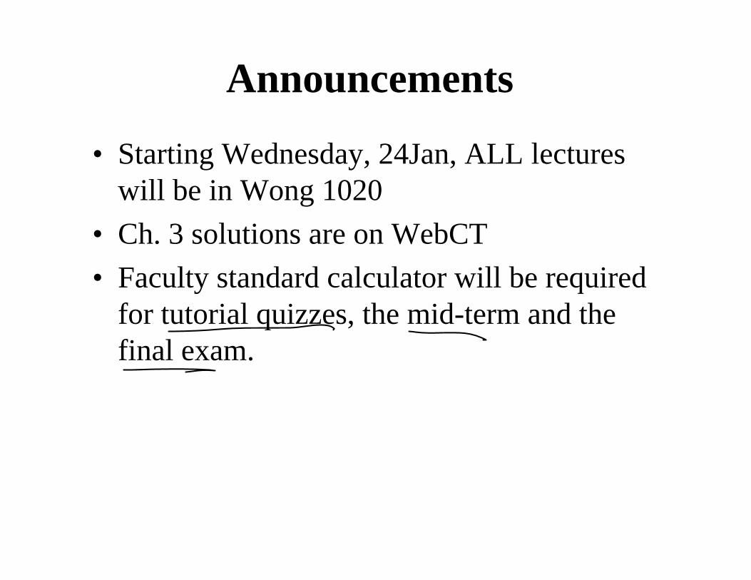
Announcements
• Starting Wednesday, 24Jan, ALL lectures will be in Wong 1020
• Ch. 3 solutions are on WebCT• Faculty standard calculator will be required
for tutorial quizzes, the mid-term and the final exam.
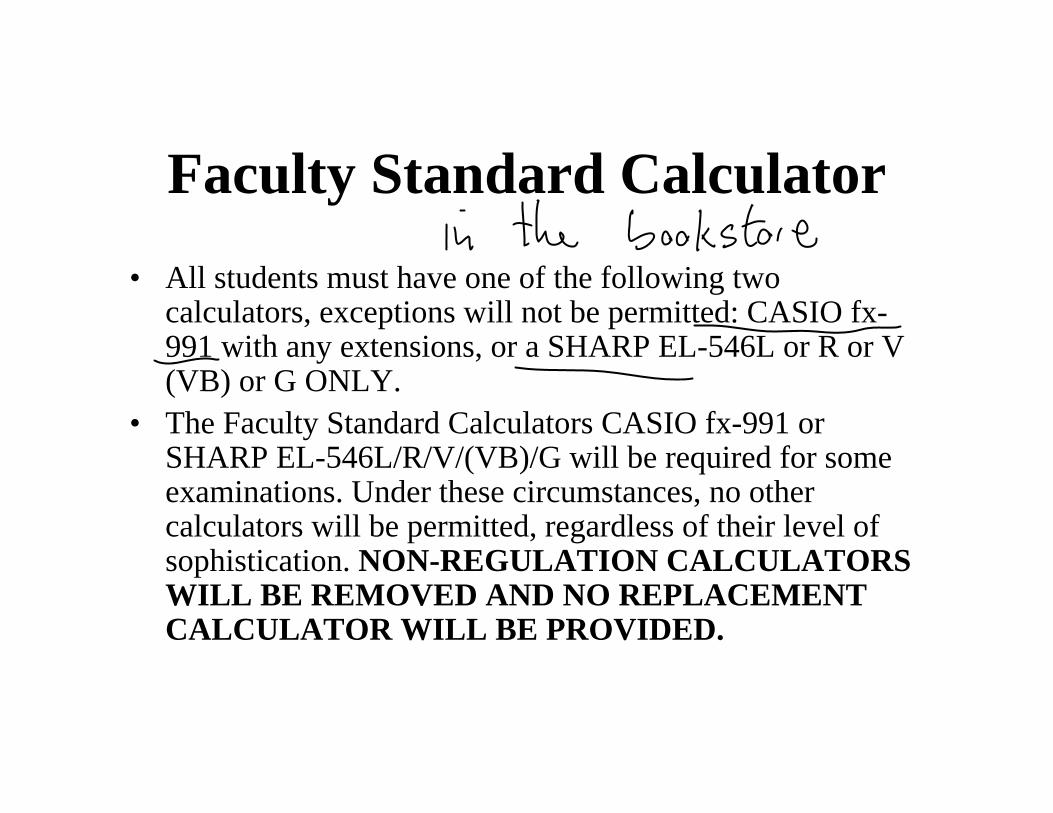
Faculty Standard Calculator• All students must have one of the following two
calculators, exceptions will not be permitted: CASIO fx-991 with any extensions, or a SHARP EL-546L or R or V (VB) or G ONLY.
• The Faculty Standard Calculators CASIO fx-991 or SHARP EL-546L/R/V/(VB)/G will be required for some examinations. Under these circumstances, no other calculators will be permitted, regardless of their level of sophistication. NON-REGULATION CALCULATORS WILL BE REMOVED AND NO REPLACEMENT CALCULATOR WILL BE PROVIDED.
Announcements
• Lots of anxiety on the quizzes?– A WebCT quiz covers concepts
• Best study aids are the lectures and the book• Covers previous week of lectures (Wed – Wed)
– A tutorial quiz covers problem solving• Best study aid is the homework• Covers previous week of lectures (Mon – Mon)• May be similar to problems worked on in tutorial

Summary of 1D Defects
• Line (edge) dislocation involves extra ½-plane of atoms. BV ⊥ to dislocation line.
• Screw dislocation involves shearing of lattice, helical arrangement of atoms. BV || to dislocation line.
• Mixed dislocation involves both previous types, complex arrangment of atoms. BV neither || or ⊥ to dislocation line.
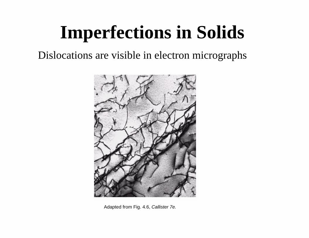
Imperfections in SolidsDislocations are visible in electron micrographs
Adapted from Fig. 4.6, Callister 7e.
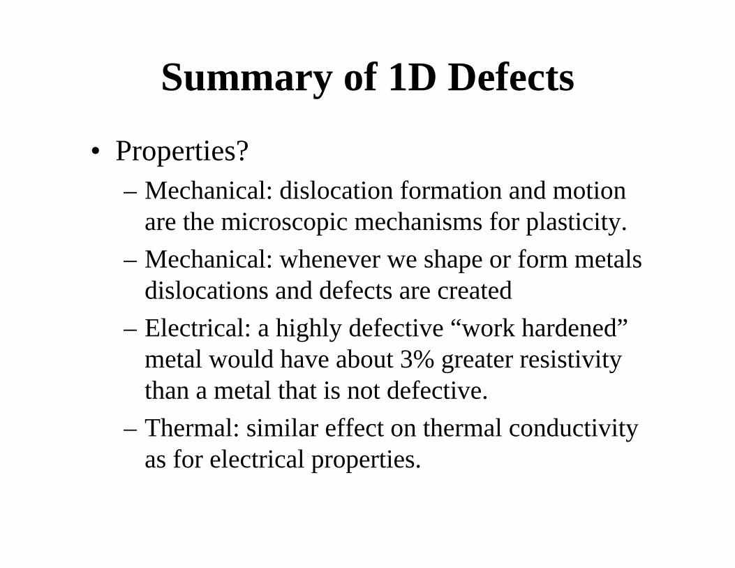
Summary of 1D Defects
• Properties?– Mechanical: dislocation formation and motion
are the microscopic mechanisms for plasticity.– Mechanical: whenever we shape or form metals
dislocations and defects are created– Electrical: a highly defective “work hardened”
metal would have about 3% greater resistivitythan a metal that is not defective.
– Thermal: similar effect on thermal conductivity as for electrical properties.
Planar (2-D) Defects
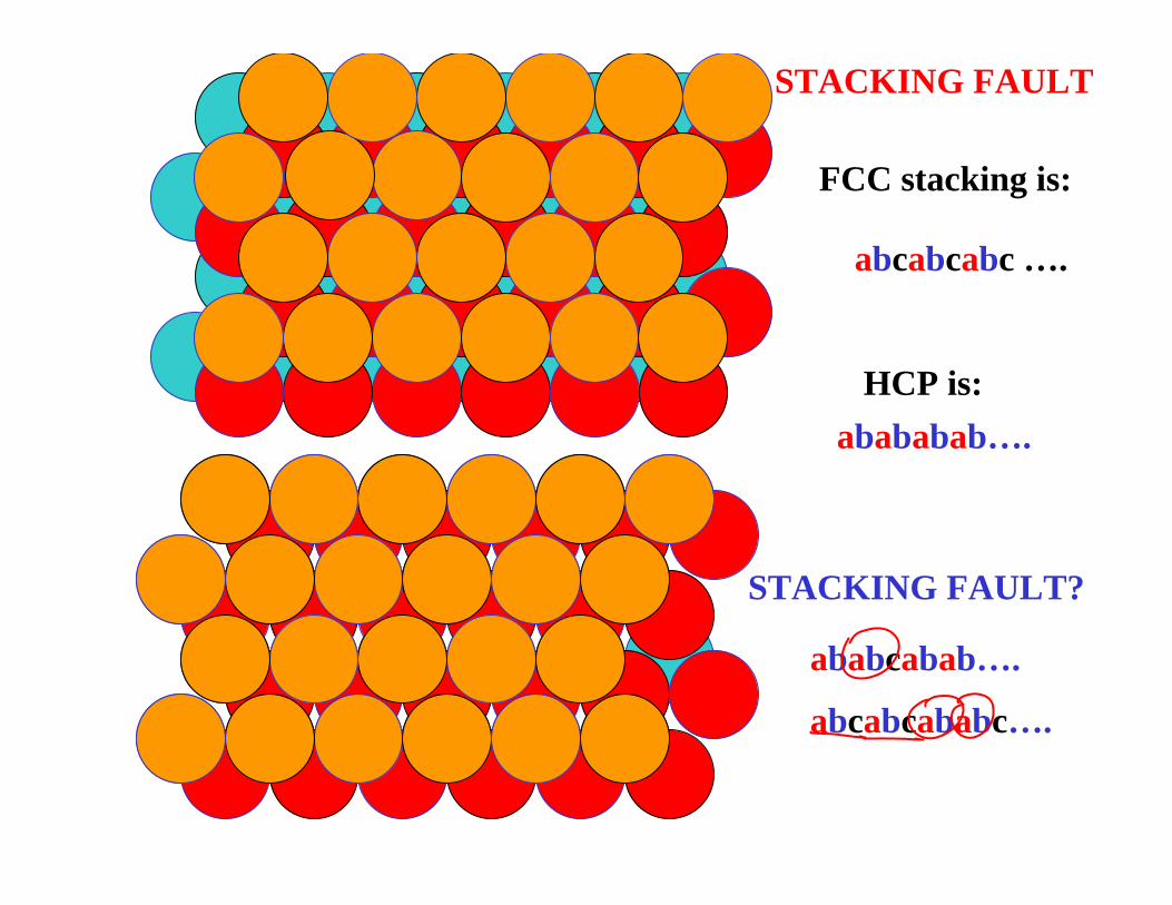
FCC stacking is:
HCP is:
abcabcabc ….
ababcabab….
STACKING FAULT
abcabcababc….
abababab….
STACKING FAULT?

Planar (2-D) Defects (cont.)Grain Boundaries (GBs)Interfaces between crystals
characterized by relative differences in crystal orientation
Low angle boundary
high angle boundary
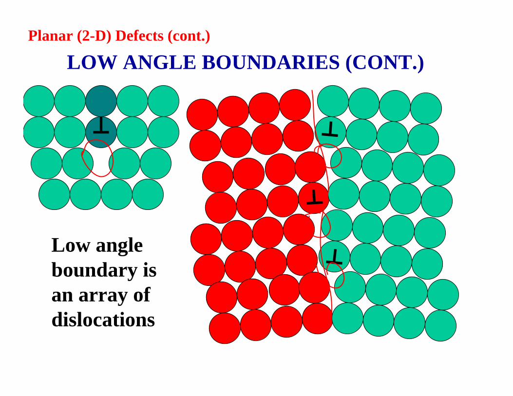
Low angle boundary is an array of dislocations
LOW ANGLE BOUNDARIES (CONT.)Planar (2-D) Defects (cont.)

are low angle boundaries
Sub-grain boundaries
Often occur within grains with high angle boundaries
High angle
Sub-grain boundary
Planar (2-D) Defects (cont.)
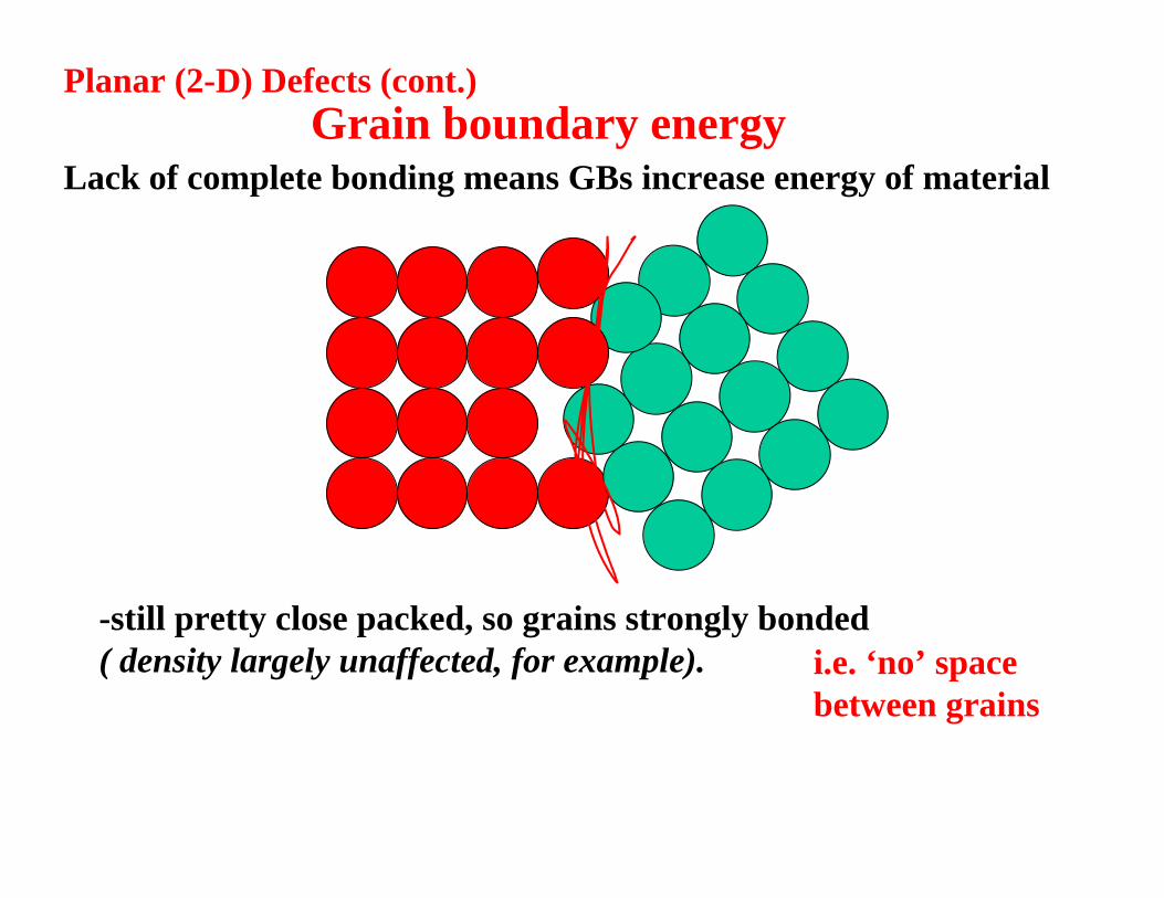
Grain boundary energy
-still pretty close packed, so grains strongly bonded ( density largely unaffected, for example).
Lack of complete bonding means GBs increase energy of material
Planar (2-D) Defects (cont.)
i.e. ‘no’ space between grains
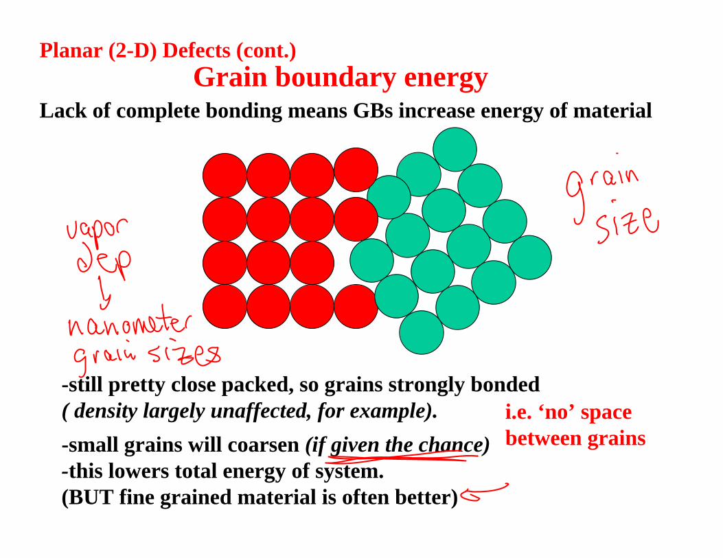
-small grains will coarsen (if given the chance)-this lowers total energy of system.(BUT fine grained material is often better)
Grain boundary energy
-still pretty close packed, so grains strongly bonded ( density largely unaffected, for example).
Lack of complete bonding means GBs increase energy of material
Planar (2-D) Defects (cont.)
i.e. ‘no’ space between grains

Twin BoundaryBoundary separating mirror images of crystals
(180 deg translation about the twin axis)
Planar (2-D) Defects (cont.)
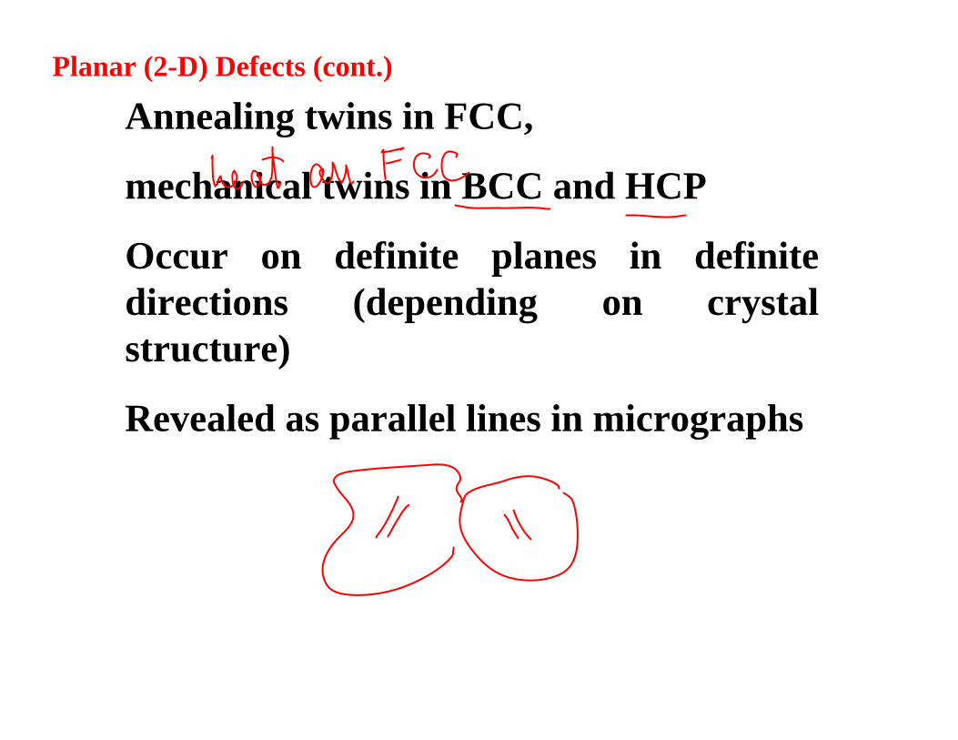
Annealing twins in FCC,
mechanical twins in BCC and HCP
Occur on definite planes in definite directions (depending on crystal structure)
Revealed as parallel lines in micrographs
Planar (2-D) Defects (cont.)
Other interfacial defectsPhase boundaries: boundary between different phases
External surfaceConsidered an imperfection because it's where the crystal terminates.
NOTE:All interfaces increase energy of material …..because atoms at interfaces aren't stabilized by electron sharing/exchange strategies.(incomplete bonding)
Planar (2-D) Defects (cont.)
BULK OR VOLUME DEFECTS(MACRO DEFECTS?)
Pores, foreign inclusions, cracks.
Very influential and detrimental category of defect.
Processing of materials can avoid these, but sometimes cannot be avoided.
If present, will ‘override’ props of materials.
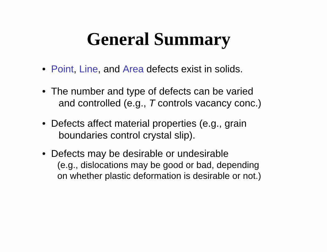
• Point, Line, and Area defects exist in solids.
• The number and type of defects can be variedand controlled (e.g., T controls vacancy conc.)
• Defects affect material properties (e.g., grainboundaries control crystal slip).
• Defects may be desirable or undesirable(e.g., dislocations may be good or bad, dependingon whether plastic deformation is desirable or not.)
General Summary
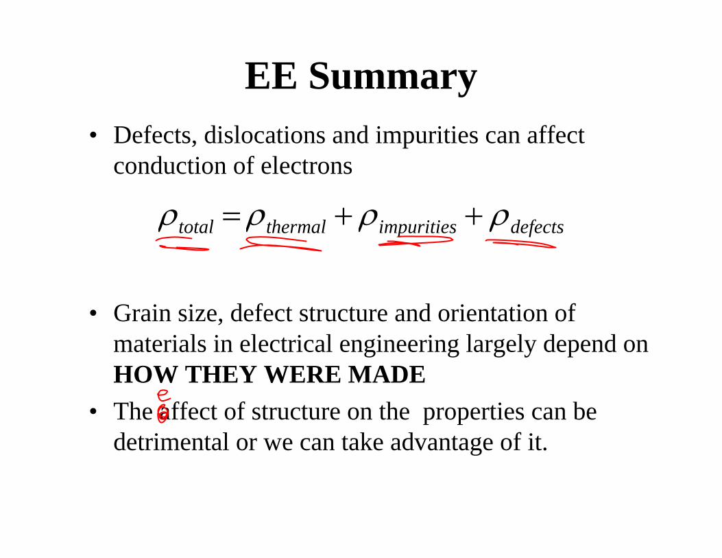
EE Summary• Defects, dislocations and impurities can affect
conduction of electrons
• Grain size, defect structure and orientation of materials in electrical engineering largely depend on HOW THEY WERE MADE
• The affect of structure on the properties can be detrimental or we can take advantage of it.
defectsimpuritiesthermaltotal ρρρρ ++=
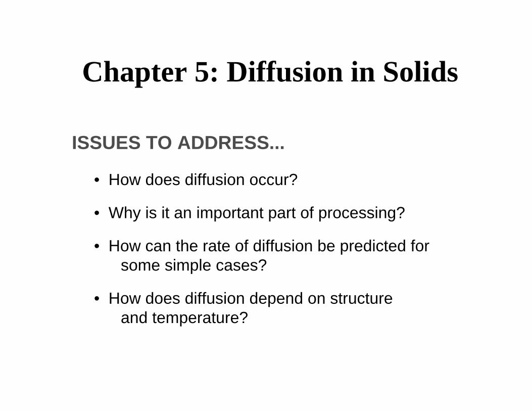
ISSUES TO ADDRESS...
• How does diffusion occur?
• Why is it an important part of processing?
• How can the rate of diffusion be predicted forsome simple cases?
• How does diffusion depend on structureand temperature?
Chapter 5: Diffusion in Solids

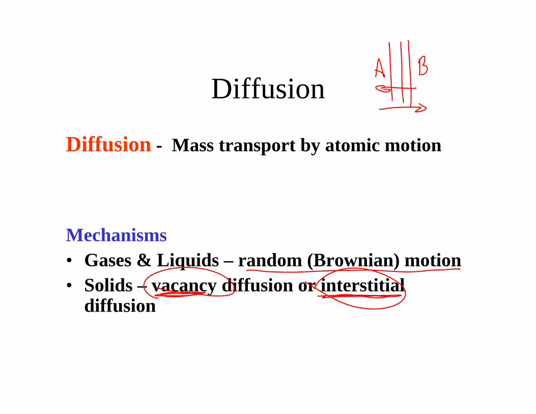
Diffusion
Diffusion - Mass transport by atomic motion
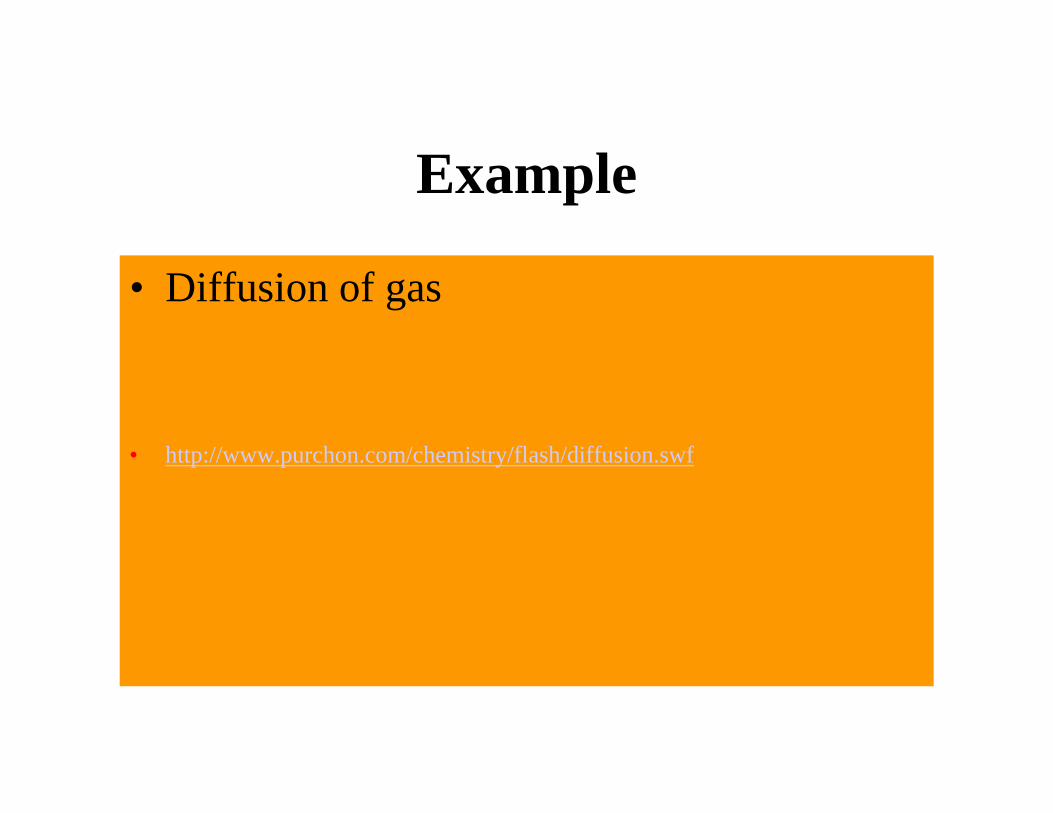
Example
• Diffusion of gas
• http://www.purchon.com/chemistry/flash/diffusion.swf

• Self-diffusion: In an elemental solid, atomsalso migrate.
Label some atoms After some time
Diffusion
A
B
C
DA
B
C
D

• Interdiffusion: In an alloy, atoms tend to migratefrom regions of high conc. to regions of low conc.
Initially
Adapted from Figs. 5.1 and 5.2, Callister 7e.
Diffusion
After some time
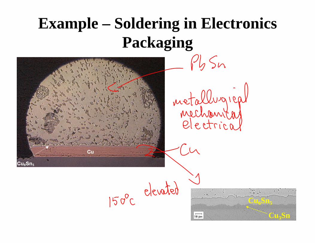
Example – Soldering in Electronics Packaging
Cu6Sn5
Cu3Sn
Diffusion
Diffusion - Mass transport by atomic motion
Mechanisms• Gases & Liquids – random (Brownian) motion• Solids – vacancy diffusion or interstitial
diffusion

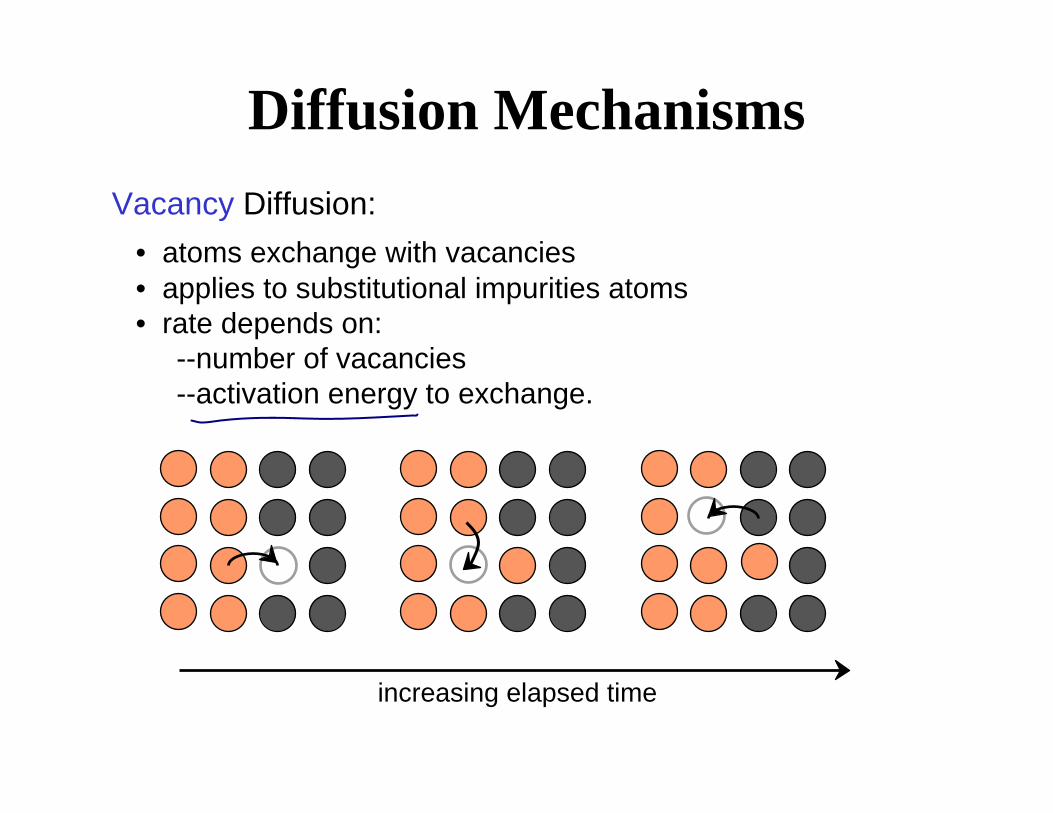
Diffusion MechanismsVacancy Diffusion:
• atoms exchange with vacancies• applies to substitutional impurities atoms • rate depends on:
--number of vacancies--activation energy to exchange.
increasing elapsed time

• Simulation of interdiffusionacross an interface:
• Rate of substitutionaldiffusion depends on:--vacancy concentration--frequency of jumping.
(Courtesy P.M. Anderson)
Diffusion Simulation

Diffusion Mechanisms• Interstitial diffusion – smaller atoms
can diffuse between atoms.
More rapid than vacancy diffusionAdapted from Fig. 5.3 (b), Callister 7e.
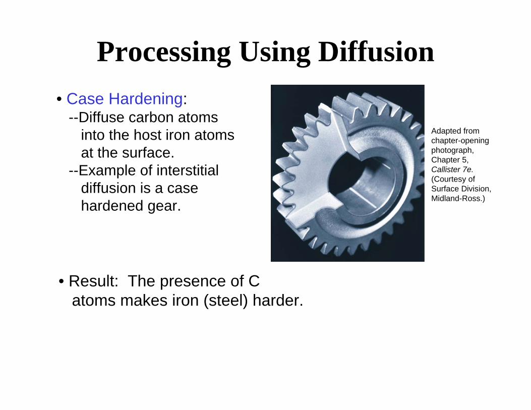
Adapted from chapter-opening photograph, Chapter 5, Callister 7e. (Courtesy ofSurface Division, Midland-Ross.)
• Case Hardening:--Diffuse carbon atoms
into the host iron atomsat the surface.
--Example of interstitialdiffusion is a casehardened gear.
• Result: The presence of C atoms makes iron (steel) harder.
Processing Using Diffusion

• Doping silicon with phosphorus for n-type semiconductors:• Process:
3. Result: Dopedsemiconductorregions.
silicon
Processing Using Diffusion
magnified image of a computer chip
0.5mm
light regions: Si atoms
light regions: Al atoms
2. Heat it.
1. Deposit P richlayers on surface.
silicon
Adapted from chapter-opening photograph, Chapter 18, Callister 7e.
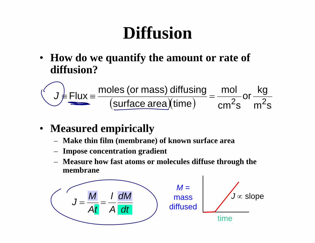
Diffusion• How do we quantify the amount or rate of
diffusion?
• Measured empirically– Make thin film (membrane) of known surface area– Impose concentration gradient– Measure how fast atoms or molecules diffuse through the
membrane
( )( ) smkgor
scmmol
timearea surfacediffusing mass) (or molesFlux 22=≡≡J
dtdM
Al
AtMJ ==
M =mass
diffusedtime
J ∝ slope
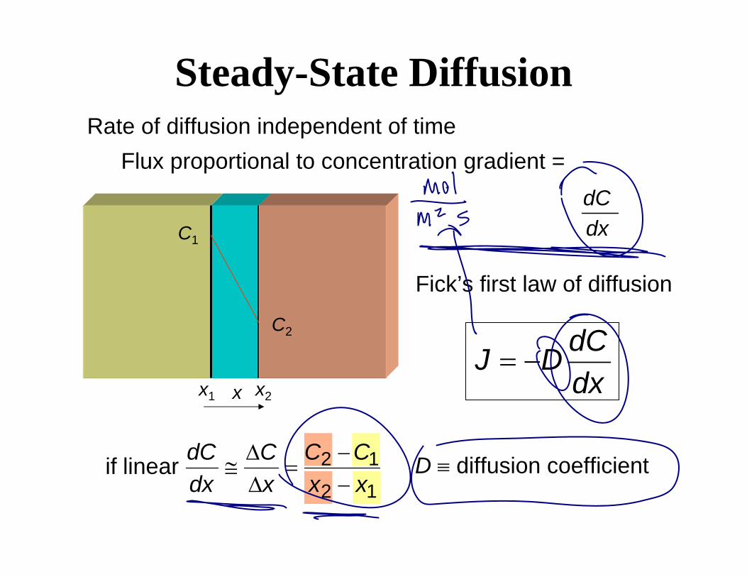
Steady-State Diffusion
dxdCDJ −=
Fick’s first law of diffusion
C1
C2
x
C1
x1 x2
D ≡ diffusion coefficient
Rate of diffusion independent of timeFlux proportional to concentration gradient =
dxdC
12
12 linear ifxxCC
xC
dxdC
−−
=ΔΔ
≅
C2

• Analyze the units of Fick’s first law for next time.