Creating Greater Capacity on Smaller Spaces - HKSTP · Creating Greater Capacity on Smaller Spaces...
28
Creating Greater Capacity on Smaller Spaces Nanofabrication and Its Impact on Sensor Manufacturing 2017-09-08
Transcript of Creating Greater Capacity on Smaller Spaces - HKSTP · Creating Greater Capacity on Smaller Spaces...
Creating Greater Capacity
on Smaller Spaces
Nanofabrication and Its Impact on Sensor Manufacturing2017-09-08
Nanofabrication and Its Impact on Sensor Manufacturing, 2017-09-08 - © Obducat 2017 CONFIDENTIAL
The context of Smart City and IoT

Nanofabrication and Its Impact on Sensor Manufacturing, 2017-09-08 - © Obducat 2017 CONFIDENTIAL
Artifical Intelligence drivning the need for new smart devices
2000 2010 2016
PC Era
Mobile Era
AI Era
Encompasses:Internet of ThingsAutonumos VechiclesBig DataCloudAR/VR
Nanofabrication and Its Impact on Sensor Manufacturing, 2017-09-08 - © Obducat 2017 CONFIDENTIAL
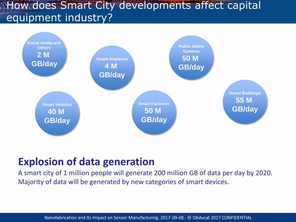
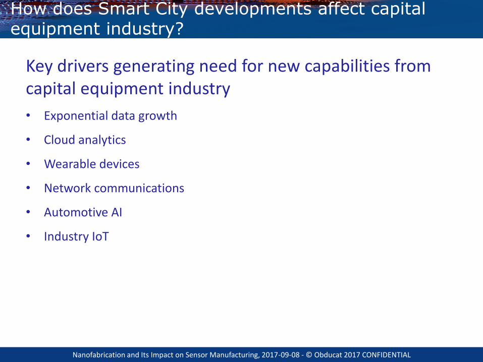
How does Smart City developments affect capitalequipment industry?
Explosion of data generationA smart city of 1 million people will generate 200 million GB of data per day by 2020.Majority of data will be generated by new categories of smart devices.
Social media and
Others
2 M
GB/daySmart Airplanes
4 M
GB/day
Smart Vehicles
40 M
GB/day
Smart Factories
50 M
GB/day
Public Safety
Systems
50 M
GB/day
Smart Buildings
55 M
GB/day
Nanofabrication and Its Impact on Sensor Manufacturing, 2017-09-08 - © Obducat 2017 CONFIDENTIAL
Key drivers generating need for new capabilities from capital equipment industry
• Exponential data growth
• Cloud analytics
• Wearable devices
• Network communications
• Automotive AI
• Industry IoT
How does Smart City developments affect capitalequipment industry?
Nanofabrication and Its Impact on Sensor Manufacturing, 2017-09-08 - © Obducat 2017 CONFIDENTIAL
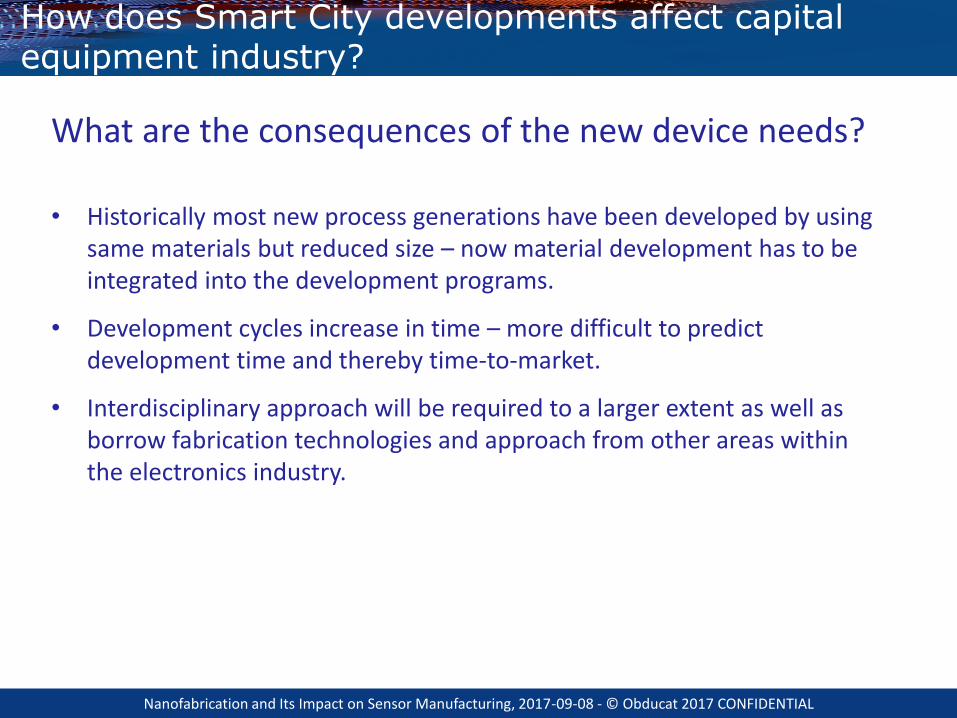
What are the consequences of the new device needs?
• Historically most new process generations have been developed by using same materials but reduced size – now material development has to be integrated into the development programs.
• Development cycles increase in time – more difficult to predict development time and thereby time-to-market.
• Interdisciplinary approach will be required to a larger extent as well as borrow fabrication technologies and approach from other areas within the electronics industry.
How does Smart City developments affect capitalequipment industry?
Nanofabrication and Its Impact on Sensor Manufacturing, 2017-09-08 - © Obducat 2017 CONFIDENTIAL
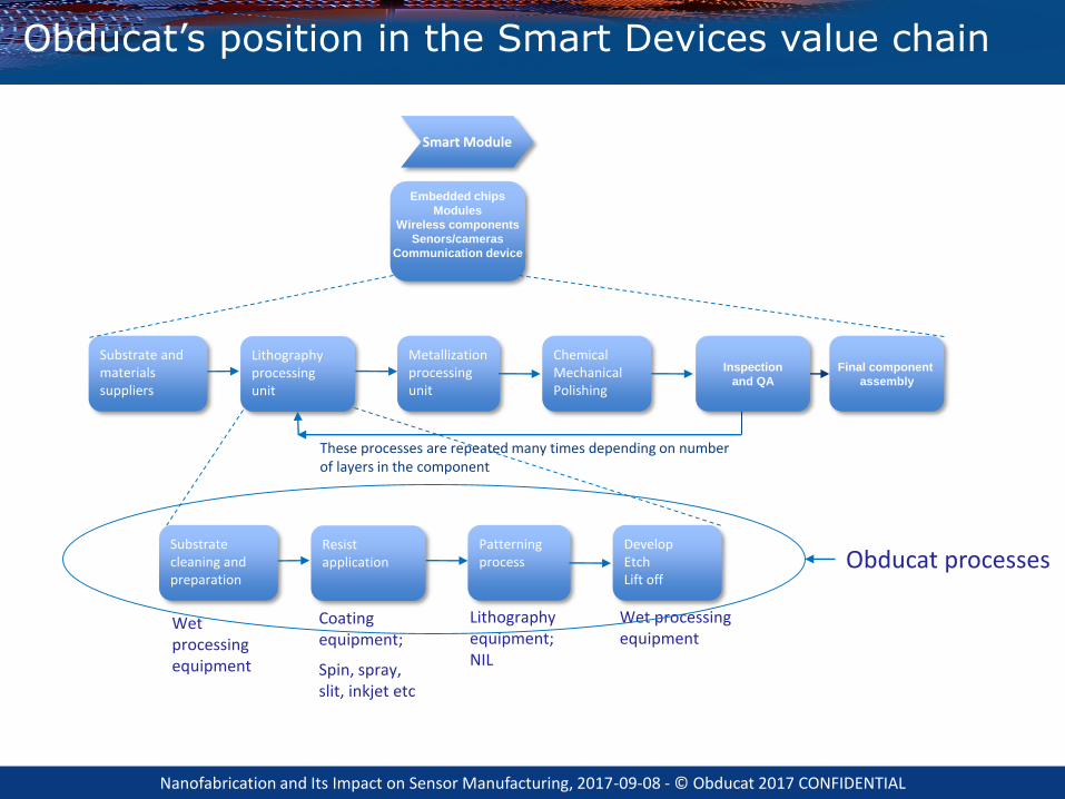
Smart Module
Embedded chips
Modules
Wireless components
Senors/cameras
Communication device
Obducat’s position in the Smart Devices value chain
Substrate and materials suppliers
Lithography processing unit
Metallization processing unit
Chemical Mechanical Polishing
These processes are repeated many times depending on number of layers in the component
Inspection
and QA
Final component
assembly
Substrate cleaning and preparation
Resist application
Patterning process
Develop Etch Lift off
Wet processing equipment
Coating equipment;
Spin, spray, slit, inkjet etc
Lithography equipment;NIL
Wet processing equipment
Obducat processes

Nanofabrication and Its Impact on Sensor Manufacturing, 2017-09-08 - © Obducat 2017 CONFIDENTIAL
Obducat Group Overview
Nanofabrication and Its Impact on Sensor Manufacturing, 2017-09-08 - © Obducat 2017 CONFIDENTIAL
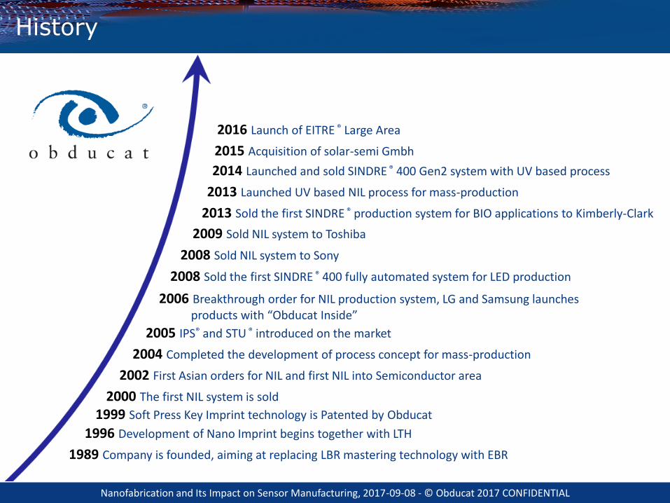
History
1989 Company is founded, aiming at replacing LBR mastering technology with EBR
1996 Development of Nano Imprint begins together with LTH
1999 Soft Press Key Imprint technology is Patented by Obducat
2000 The first NIL system is sold
2002 First Asian orders for NIL and first NIL into Semiconductor area
2004 Completed the development of process concept for mass-production
2005 IPS® and STU ® introduced on the market
2006 Breakthrough order for NIL production system, LG and Samsung launchesproducts with “Obducat Inside”
2008 Sold the first SINDRE ® 400 fully automated system for LED production
2013 Sold the first SINDRE ® production system for BIO applications to Kimberly-Clark
2013 Launched UV based NIL process for mass-production
2014 Launched and sold SINDRE ® 400 Gen2 system with UV based process
2016 Launch of EITRE ® Large Area
2015 Acquisition of solar-semi Gmbh
2008 Sold NIL system to Sony
2009 Sold NIL system to Toshiba
Nanofabrication and Its Impact on Sensor Manufacturing, 2017-09-08 - © Obducat 2017 CONFIDENTIAL
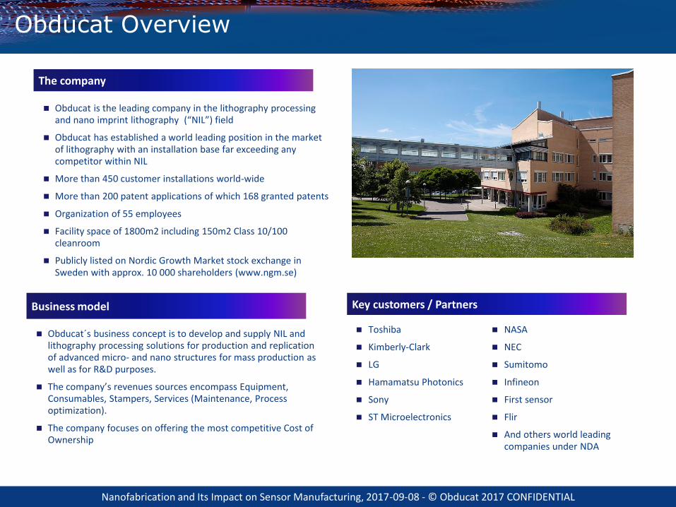
Business model
Obducat´s business concept is to develop and supply NIL and lithography processing solutions for production and replication of advanced micro- and nano structures for mass production as well as for R&D purposes.
The company’s revenues sources encompass Equipment, Consumables, Stampers, Services (Maintenance, Process optimization).
The company focuses on offering the most competitive Cost of Ownership
Key customers / Partners
Toshiba
Kimberly-Clark
LG
Hamamatsu Photonics
Sony
ST Microelectronics
NASA
NEC
Sumitomo
Infineon
First sensor
Flir
And others world leading companies under NDA
Obducat is the leading company in the lithography processing and nano imprint lithography (“NIL”) field
Obducat has established a world leading position in the market of lithography with an installation base far exceeding any competitor within NIL
More than 450 customer installations world-wide
More than 200 patent applications of which 168 granted patents
Organization of 55 employees
Facility space of 1800m2 including 150m2 Class 10/100 cleanroom
Publicly listed on Nordic Growth Market stock exchange in Sweden with approx. 10 000 shareholders (www.ngm.se)
The company
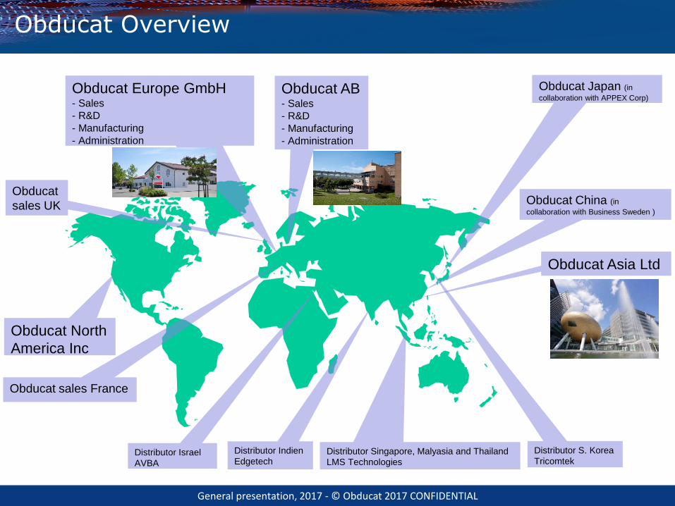
Obducat Overview
General presentation, 2017 - © Obducat 2017 CONFIDENTIAL
Obducat AB - Sales
- R&D
- Manufacturing
- Administration
Obducat China (in
collaboration with Business Sweden )
Obducat Japan (in
collaboration with APPEX Corp)
Distributor S. Korea
TricomtekDistributor Indien
EdgetechDistributor Israel
AVBA
Distributor Singapore, Malyasia and Thailand
LMS Technologies
Obducat Europe GmbH - Sales
- R&D
- Manufacturing
- Administration
Obducat
sales UK
Obducat North
America Inc
Obducat sales France
Obducat Asia Ltd
Obducat Overview
Nanofabrication and Its Impact on Sensor Manufacturing, 2017-09-08 - © Obducat 2017 CONFIDENTIAL
Obducat NIL technology
Nanofabrication and Its Impact on Sensor Manufacturing, 2017-09-08 - © Obducat 2017 CONFIDENTIAL
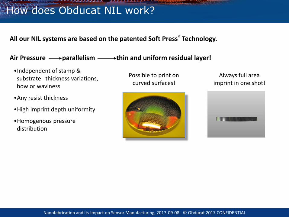
All our NIL systems are based on the patented Soft Press® Technology.
Air Pressure parallelism thin and uniform residual layer!
How does Obducat NIL work?
•Independent of stamp & substrate thickness variations, bow or waviness
•Any resist thickness
•High Imprint depth uniformity
•Homogenous pressure distribution
Always full area imprint in one shot!
Possible to print on curved surfaces!
Nanofabrication and Its Impact on Sensor Manufacturing, 2017-09-08 - © Obducat 2017 CONFIDENTIAL
Obducat Group Product Portfolio
Nanofabrication and Its Impact on Sensor Manufacturing, 2017-09-08 - © Obducat 2017 CONFIDENTIAL
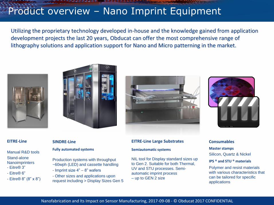
Utilizing the proprietary technology developed in-house and the knowledge gained from application development projects the last 20 years, Obducat can offer the most comprehensive range of lithography solutions and application support for Nano and Micro patterning in the market.
Product overview – Nano Imprint Equipment
EITRE-Line
Manual R&D tools
Stand-alone
Nanoimprinters
- Eitre® 3”
- Eitre® 6”
- Eitre® 8” (8” x 8”)
EITRE-Line Large Substrates
Semiautomatic systems
NIL tool for Display standard sizes up
to Gen 2. Suitable for both Thermal,
UV and STU processes. Semi-
automatic imprint process
– up to GEN 2 size
SINDRE-Line
Fully automated systems
Production systems with throughput
~60wph (LED) and cassette handling
- Imprint size 4” – 8” wafers
- Other sizes and applications upon
request including > Display Sizes Gen 5
Consumables
Master stamps
Silicon, Quartz & Nickel
IPS ® and STU ® materials
Polymer and resist materials
with various characteristics that
can be tailored for specific
applications
Nanofabrication and Its Impact on Sensor Manufacturing, 2017-09-08 - © Obducat 2017 CONFIDENTIAL
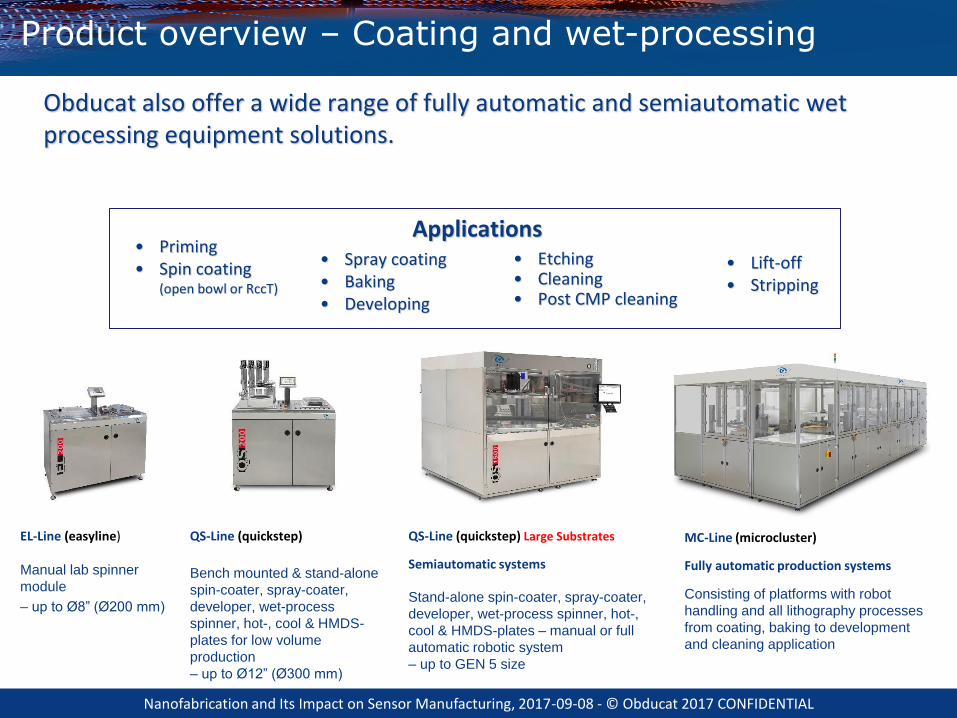
Obducat also offer a wide range of fully automatic and semiautomatic wet processing equipment solutions.
Applications
Product overview – Coating and wet-processing
• Priming• Spin coating
(open bowl or RccT)
• Spray coating• Baking• Developing
• Lift-off• Stripping
• Etching• Cleaning• Post CMP cleaning
EL-Line (easyline)
Manual lab spinner
module
– up to Ø8” (Ø200 mm)
QS-Line (quickstep) Large Substrates
Semiautomatic systems
Stand-alone spin-coater, spray-coater,
developer, wet-process spinner, hot-,
cool & HMDS-plates – manual or full
automatic robotic system
– up to GEN 5 size
QS-Line (quickstep)
Bench mounted & stand-alone
spin-coater, spray-coater,
developer, wet-process
spinner, hot-, cool & HMDS-
plates for low volume
production
– up to Ø12” (Ø300 mm)
MC-Line (microcluster)
Fully automatic production systems
Consisting of platforms with robot
handling and all lithography processes
from coating, baking to development
and cleaning application

Nanofabrication and Its Impact on Sensor Manufacturing, 2017-09-08 - © Obducat 2017 CONFIDENTIAL
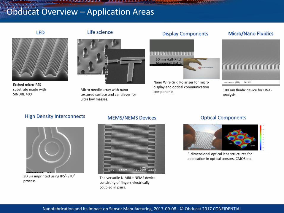
Obducat Overview –Application Areas
Nanofabrication and Its Impact on Sensor Manufacturing, 2017-09-08 - © Obducat 2017 CONFIDENTIAL
Micro/Nano Fluidics
50 nm Half-Pitch Aluminum Pattern
Display Components
Nano Wire Grid Polarizer for micro display and optical communication components.
High Density Interconnects
3D via imprinted using IPS®-STU®
process.
MEMS/NEMS Devices
The versatile NIMBLe NEMS device consisting of fingers electrically coupled in pairs.
Optical Components
3-dimensional optical lens structures for application in optical sensors, CMOS etc.
Obducat Overview – Application Areas
Life science
Micro needle array with nanotextured surface and cantilever for ultra low masses.
Etched micro-PSS substrate made with SINDRE 400
LED Micro/Nano Fluidics
100 nm fluidic device for DNA-analysis.
Nanofabrication and Its Impact on Sensor Manufacturing, 2017-09-08 - © Obducat 2017 CONFIDENTIAL
Optical Applications
Nanofabrication and Its Impact on Sensor Manufacturing, 2017-09-08 - © Obducat 2017 CONFIDENTIAL
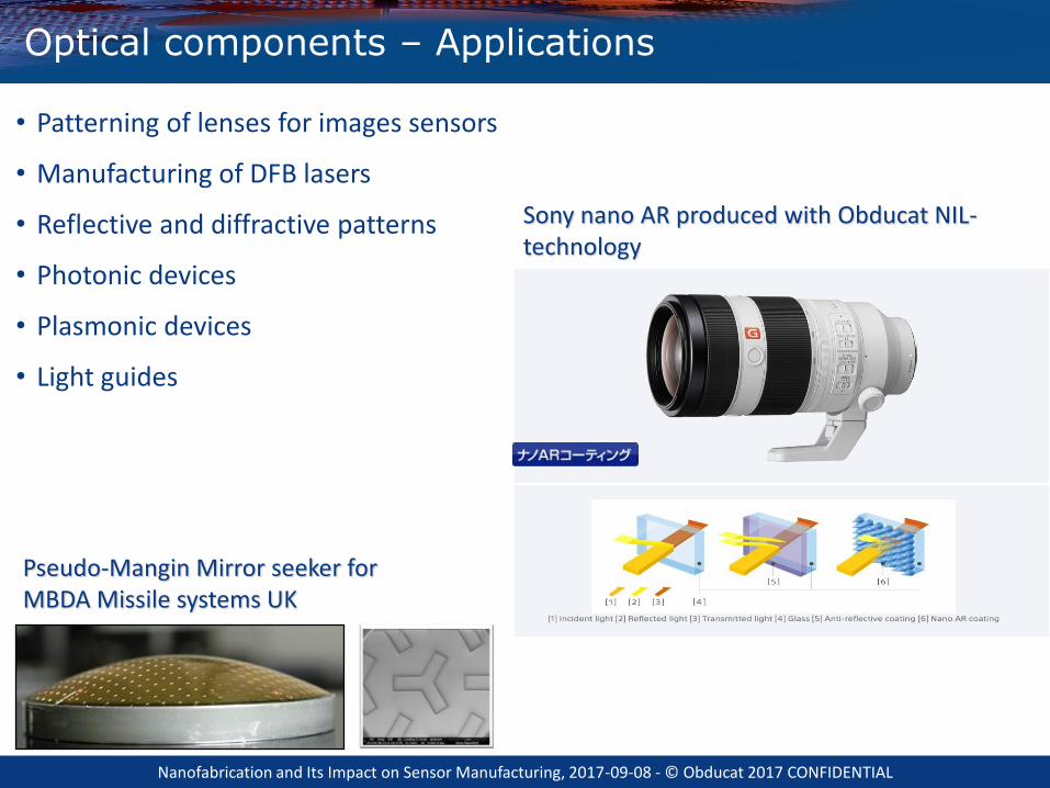
Pseudo-Mangin Mirror seeker for MBDA Missile systems UK
Sony nano AR produced with Obducat NIL-technology
Optical components – Applications
• Patterning of lenses for images sensors
• Manufacturing of DFB lasers
• Reflective and diffractive patterns
• Photonic devices
• Plasmonic devices
• Light guides

Nanofabrication and Its Impact on Sensor Manufacturing, 2017-09-08 - © Obducat 2017 CONFIDENTIAL
Life science applications
Nanofabrication and Its Impact on Sensor Manufacturing, 2017-09-08 - © Obducat 2017 CONFIDENTIAL
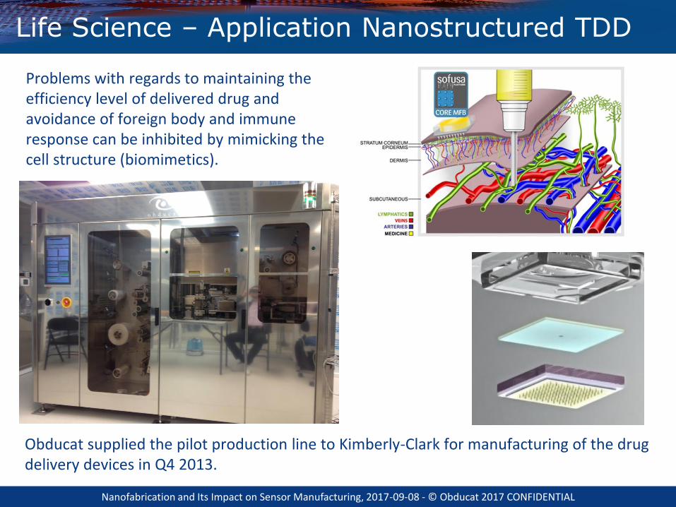
Obducat supplied the pilot production line to Kimberly-Clark for manufacturing of the drug delivery devices in Q4 2013.
Problems with regards to maintaining the efficiency level of delivered drug and avoidance of foreign body and immune response can be inhibited by mimicking the cell structure (biomimetics).
Life Science – Application Nanostructured TDD
Nanofabrication and Its Impact on Sensor Manufacturing, 2017-09-08 - © Obducat 2017 CONFIDENTIAL
Display Application
Nanofabrication and Its Impact on Sensor Manufacturing, 2017-09-08 - © Obducat 2017 CONFIDENTIAL
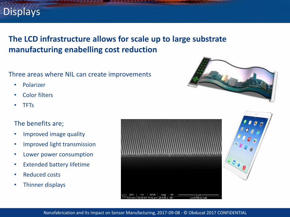
Displays
The LCD infrastructure allows for scale up to large substrate manufacturing enabelling cost reduction
Three areas where NIL can create improvements
• Polarizer
• Color filters
• TFTs
The benefits are;
• Improved image quality
• Improved light transmission
• Lower power consumption
• Extended battery lifetime
• Reduced costs
• Thinner displays
Nanofabrication and Its Impact on Sensor Manufacturing, 2017-09-08 - © Obducat 2017 CONFIDENTIAL
How can Sensor Manufacturing benefit from nanofabrication
methods
Nanofabrication and Its Impact on Sensor Manufacturing, 2017-09-08 - © Obducat 2017 CONFIDENTIAL
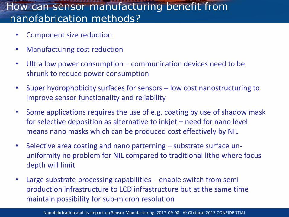
How can sensor manufacturing benefit fromnanofabrication methods?
• Component size reduction
• Manufacturing cost reduction
• Ultra low power consumption – communication devices need to be shrunk to reduce power consumption
• Super hydrophobicity surfaces for sensors – low cost nanostructuring to improve sensor functionality and reliability
• Some applications requires the use of e.g. coating by use of shadow mask for selective deposition as alternative to inkjet – need for nano level means nano masks which can be produced cost effectively by NIL
• Selective area coating and nano patterning – substrate surface un-uniformity no problem for NIL compared to traditional litho where focus depth will limit
• Large substrate processing capabilities – enable switch from semi production infrastructure to LCD infrastructure but at the same time maintain possibility for sub-micron resolution
Nanofabrication and Its Impact on Sensor Manufacturing, 2017-09-08 - © Obducat 2017 CONFIDENTIAL
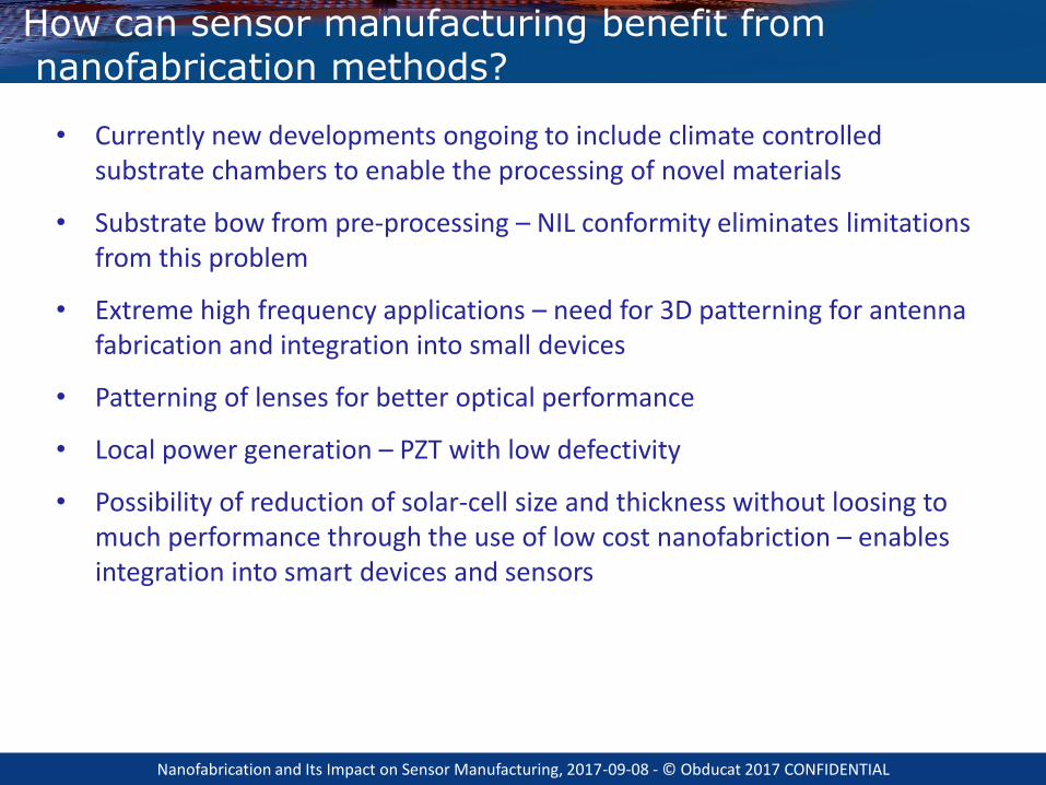
How can sensor manufacturing benefit fromnanofabrication methods?
• Currently new developments ongoing to include climate controlled substrate chambers to enable the processing of novel materials
• Substrate bow from pre-processing – NIL conformity eliminates limitations from this problem
• Extreme high frequency applications – need for 3D patterning for antenna fabrication and integration into small devices
• Patterning of lenses for better optical performance
• Local power generation – PZT with low defectivity
• Possibility of reduction of solar-cell size and thickness without loosing to much performance through the use of low cost nanofabriction – enables integration into smart devices and sensors

Nanofabrication and Its Impact on Sensor Manufacturing, 2017-09-08 - © Obducat 2017 CONFIDENTIAL
Thank You for Your attention
Patrik Lundström
Obducat AB (publ)