Conductivity in Carbon Nanotubes
16
Conductivity in Carbon Nanotubes Stephen French Abstract – Vapor deposition is explored as a means of directly lowering the resistance of thin films of carbon nanotubes. In the process, atmospheric doping of the tubes is discovered to be very important in the resistance of ultra thin carbon nanotube films and is further explored. Possible future research is described. Thin films of carbon nanotubes are optically transparent and electrically conductive. They show promise to be used in organic light emitting diodes, vertical field- effect transistors, and solar cells. Before they become competitive in the marketplace, their conductivity must be improved. The goal of this paper is to describe efforts to improve conductivities. Carbon nanotubes provide excellent conduction along the tube axis. In tight binding theory, they can be considered rolled up sheets of graphite. Graphite is composed of a hexagonal network of sp2 hybridized carbon atoms; that is, the 1s, 2px, 2py, and 2pz orbitals hybridize to form four equivalent orbitals. Three of these orbitals are involved in strong covalent bonds to other carbon atoms to form a flat hexagonal network. The remaining orbital sits perpendicular to the plane of graphite. This perpendicular orbital associates with the perpendicular orbits of the other carbon atoms exhibiting, as chemists would say, the concept of aromaticity. Simply stated, all the perpendicular orbits form a loose bond with each neighboring perpendicular orbit. This allows for the delocalization of the electron; that is, the electron density is evenly spread out across the entire surface of the graphite, and its wave function is solved across the entire sample. This is the condition for ballistic transport of the electron [1]. When the graphite is rolled up, this electronic structure is maintained. As a result, conduction along the axis of the nanotube is ballistic. Conduction between tubes is equivalent to conduction across sheets of
Transcript of Conductivity in Carbon Nanotubes
Conductivity in Carbon Nanotubes Stephen French
Abstract – Vapor deposition is explored as a means of directly lowering the resistance of
thin films of carbon nanotubes. In the process, atmospheric doping of the tubes is
discovered to be very important in the resistance of ultra thin carbon nanotube films and
is further explored. Possible future research is described.
Thin films of carbon nanotubes are optically transparent and electrically
conductive. They show promise to be used in organic light emitting diodes, vertical field-
effect transistors, and solar cells. Before they become competitive in the marketplace,
their conductivity must be improved. The goal of this paper is to describe efforts to
improve conductivities.
Carbon nanotubes provide excellent conduction along the tube axis. In tight
binding theory, they can be considered rolled up sheets of graphite. Graphite is composed
of a hexagonal network of sp2 hybridized carbon atoms; that is, the 1s, 2px, 2py, and 2pz
orbitals hybridize to form four equivalent orbitals. Three of these orbitals are involved in
strong covalent bonds to other carbon atoms to form a flat hexagonal network. The
remaining orbital sits perpendicular to the plane of graphite. This perpendicular orbital
associates with the perpendicular orbits of the other carbon atoms exhibiting, as chemists
would say, the concept of aromaticity. Simply stated, all the perpendicular orbits form a
loose bond with each neighboring perpendicular orbit. This allows for the delocalization
of the electron; that is, the electron density is evenly spread out across the entire surface
of the graphite, and its wave function is solved across the entire sample. This is the
condition for ballistic transport of the electron [1]. When the graphite is rolled up, this
electronic structure is maintained. As a result, conduction along the axis of the nanotube
is ballistic. Conduction between tubes is equivalent to conduction across sheets of
graphite. This conduction is not ballistic and it is the limiting factor in the conductivity of
thin films of carbon nanotubes [2].
Attention was primarily directed towards junctions of carbon nanotubes. A thin
film is made up of many nanotubes that range from 5-6 um long. In order for current to
pass across these films, it must make many tube-to-tube jumps. Improving the
conductivity at these junctions is a possible path to significantly improving the
conductivity of the entire film. Gold and pentacene were deposited on thin films to
attempt to provide additional conducting pathways at each junction.
Experimental Procedure:
Thin films were produced as described by Wu et al. [3] with thicknesses ranging
from that equivalent to 2nm thick film to a thickness equivalent to 25 nm. It is important
to note that as the bundles of carbon nanotubes average 5-10 nm in diameter, there is a
large deviation in the actual thickness of the film across relatively small distances. With
especially “thin” films, some regions of the substrate are not covered by the carbon
nanotubes, and the film thickness refers to an average height over the entire sample.
Films were produced in a class 100 clean room and transferred to either glass or quartz
substrates, following which, 80nm thick gold electrodes were thermally evaporated in a
vacuum chamber and deposited at the corners of the film to make electrical contact to the
film . Depositions of different materials on the thin films was done in the same vacuum
chamber. The resistance of the sheets was taken in accordance with the Vander Pauw
Method. Two sets of equipment were used. An HP E3617A DC Power Supply used in
conjunction with an HP 3478A Mulimeter and a Radioshack TRU RMS Digital
Multimeter provided about half of the measurements, while a Kiethley 2400 source meter
provided the rest. Care was taken to ensure that the two systems were in agreement.
Experiment Part 1:
The sidewalls of a carbon nanotube are very pristine. As mentioned above, the
perpendicular orbitals exhibit aromaticity and are very low energy. It is difficult to
disrupt this aromaticity and attach to the side surface. The intention was to take
advantage of this to concentrate gold molecules at the junctions. It was expected that gold
molecules would land on a sidewall and migrate along it until they arrived at junction
where the binding would be to a greater surface area and thus lead to a higher energy
bond. This is exactly the process described by Bienfait et al. for various gasses [4]. Five
nm Au was deposited on thin films of thickness equivalent to 3nm and 20 nm. The values
of the decrease in resistance are given in Table 1. Large improvements over initial
resistances can be noticed, but considerations must be made. It may be that the
conduction in the gold simply provided a parallel path that lowered the resistance. The
parallel resistance of the gold sheet and the carbon nanotube film was calculated to be a
value greater than the achieved sheet resistance in both cases. We can conclude that there
are electrical current pathways that utilize both the gold and the carbon films. We can not
discern the exact nature of this pathway, so it is impossible to know if the gold atoms are
used primarily at the junctions as was hoped for. Table 1.
CNT
thickness
(nm)
Au
deposited
(nm)
Initial Sheet
Resistance
(Ohms/sqr)
Final Sheet
Resistance
(Ohms/Sqr)
Parallel
Resistance
(ohms/Sqr)
% Decrease
3 5 34240 10500 34000 69
20 5 252 222 252 12
From the data above, it could be that the current propagates largely through the
gold. We sought electrical current paths that were dominated by the carbon nanotubes, so
the next step was to lay down a sub-percolating layer of gold. We deposited .3nm Au on
4nm equivalent thick films and 1nm Au on a 3nm thick film. The results are given in
Table II.
Table II.
CNT
thickness
(nm)
Au
deposited
(nm)
Initial Sheet
Resistance
(Ohms/sqr)
Final Sheet
Resistance
(Ohms/Sqr)
Parallel
Resistance
(ohms/Sqr)
% Decrease
3 1 48850 39140 48850 19.8
4 .3 12537 10880 12537 13.2
4 .3 12790 9360 12790 26
The data in table II show an improvement in the conductance. The gold layer was
determined to be sub-percolating by the deposition on a plain glass slide of 1 nm Au. No
current could be passed across this sheet, indicating sub percolation. Knowing that gold
pathways are limited, one can conclude that the electric current paths across the film are
dominated by carbon nanotubes.
Depositing 1nm Au on a 25nm thick film represents a treatment of a film with a
more technologically useful thickness. This was carried out to find no improvement in
sheet resistance.
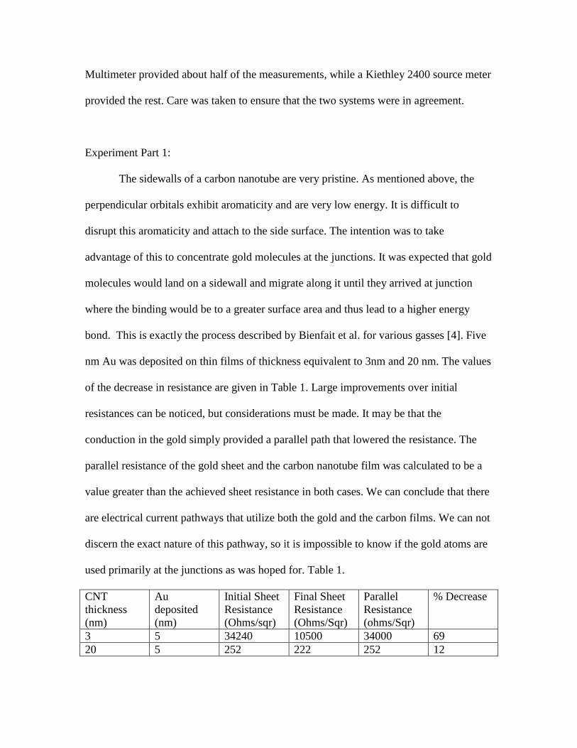
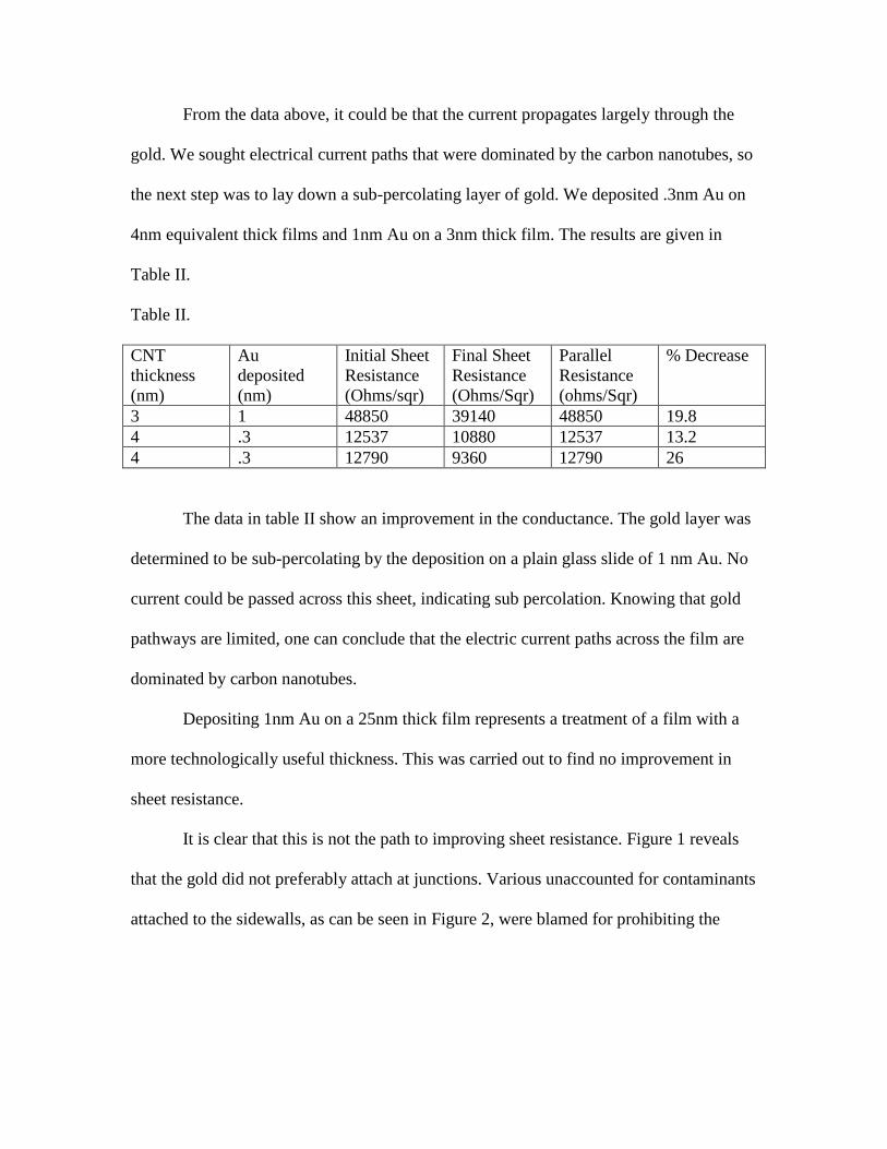
It is clear that this is not the path to improving sheet resistance. Figure 1 reveals
that the gold did not preferably attach at junctions. Various unaccounted for contaminants
attached to the sidewalls, as can be seen in Figure 2, were blamed for prohibiting the
desired migration along sidewalls.
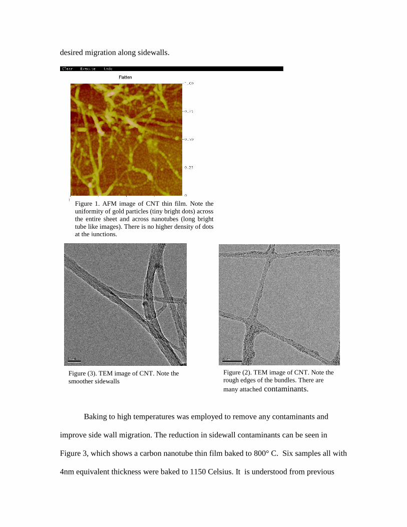
Baking to high temperatures was employed to remove any contaminants and
improve side wall migration. The reduction in sidewall contaminants can be seen in
Figure 3, which shows a carbon nanotube thin film baked to 800° C. Six samples all with
4nm equivalent thickness were baked to 1150 Celsius. It is understood from previous
Figure 1. AFM image of CNT thin film. Note the
uniformity of gold particles (tiny bright dots) across
the entire sheet and across nanotubes (long bright
tube like images). There is no higher density of dots
at the junctions.
Figure (2). TEM image of CNT. Note the
rough edges of the bundles. There are
many attached contaminants.
Figure (3). TEM image of CNT. Note the
smoother sidewalls
work in the Rinzler lab that baking significantly dedopes, or removes charge carriers,
from the films.
Experiment Part Two:
The six samples were transferred to a quartz substrate as opposed to glass in order
to withstand a high temperature bake. They were then baked under flowing argon gas in a
tube furnace over a 14 h period to a maximum temperature of 1150 C. Because the
baking would melt gold electrodes, sheet resistance could not be taken before the baking.
At the completion of the baking, the tubes were moved to an argon filled glovebox for
electrode deposition. During the move, the tubes were exposed to atmosphere for
approximately 45 sec. Sheet resistance measurements were taken as soon as the gold
electrodes had been deposited, again in an inert glovebox. One nano-meter of gold was
then deposited on two of the films, one nano-meter of pentacene on the other two, and the
other two samples were left alone. One of the samples upon which nothing was deposited
was damaged before any useful readings could be taken.
One Nanometer of Gold: samples T and N
It is interesting to note that the resistance of these sheets did not improve upon
deposition of gold. This result can be viewed in appendix 1 and 2 and is inconsistent with
results from sample set 2. There exist two differences between the treatment of sample
set 2 and sample set 3. Sample set 2 was unbaked and was exposed to atmosphere during
the measurement process while sample set three was baked and exposed only to a
nitrogen environment during the process. An additional sample, sample 10, was created

to resolve the inconsistencies from sample set 2 and sample set 3. Sample 10 was not
baked and exposed only to the nitrogen atmosphere. Gold deposition lowered its sheet
resistance, and this leads to the conclusion that sample set three saw no improvement in
sheet resistance because it was baked. The baking and subsequent removal of the sidewall
contaminants improved tube-to-tube contact such that the improvement gained by the
presence of a sub percolating layer of gold was negligible. Figure 4 provides some insight
as to the reason for no improvement as it reveals that the baking did not induce the gold
to flow along the nanotube surfaces until a junction was reached.
One Nanometer of Pentacene: Samples 1 and 7
Pentacene molecules consist of five hexagons of carbon with each hexagon
exhibiting aromaticity similar to a segment of a graphite sheet. Graphite is often used as a
lubricant because the two different sheets of graphite slide across each other very easily.
Figure 4. AFM image of CNT thin film. Note the
uniformity of gold particles (tiny bright dots)
across the entire sheet and across nanotubes
(long bright tube like images). There is no higher
density of dots at the junctions.

This is because the interface of the graphite involves two extended networks of
nonlocalized aromatized orbitals. These are very low in energy and do not readily bond
with each other. The same effect was hoped for with the pentacene. Its aromatized
perpendicular orbitals (described earlier in the paper) should interact with the aromatized
carbon nanotube sidewalls in much the same way the two sheets of graphite interact. This
should allow for the pentacene to lightly attach to the side walls and readily slide around
until a junction is reached.
Figure 5 shows that the above mentioned mechanism did function.
While favorable mechanical behavior of the pentacene on the surface of the
carbon nanotubes was observed, measurements of resistance before and after yielded no
Figure 5. AFM image of pentacene deposited on
CNT thin film. indicates that the pentacene did
show preference to the junction. Notice that
junctions are not visible and are covered by
pentacene while tube surfaces remain completely
clear.
significant gains in the conductivity of the films, as shown in appendix 3 and 4. The
similarity between conduction across a nanotube junction and a pentacene-nanotube
junction explains this result [5]. Electronic transition across a carbon nanotube junction
utilizes perpendicular orbitals very similar to those of pentacene. The contact resistance
between the two different junctions should be very close and current does not find an
easier pathway. It is true that more pathways of the same resistance should yield better
conductivity, but any path between nanotubes will require one transition while a path
including pentacene will include at least two transitions and likely more.
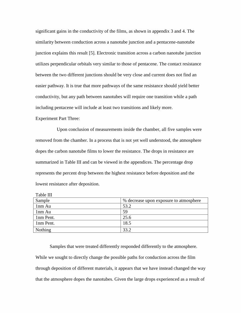
Experiment Part Three:
Upon conclusion of measurements inside the chamber, all five samples were
removed from the chamber. In a process that is not yet well understood, the atmosphere
dopes the carbon nanotube films to lower the resistance. The drops in resistance are
summarized in Table III and can be viewed in the appendices. The percentage drop
represents the percent drop between the highest resistance before deposition and the
lowest resistance after deposition.
Table III
Sample % decrease upon exposure to atmosphere
1nm Au 53.2
1nm Au 59
1nm Pent. 25.6
1nm Pent. 18.5
Nothing 33.2
Samples that were treated differently responded differently to the atmosphere.
While we sought to directly change the possible paths for conduction across the film
through deposition of different materials, it appears that we have instead changed the way
that the atmosphere dopes the nanotubes. Given the large drops experienced as a result of

doping and the differences in the magnitude of doping for different depositions, it is
important to understand this process as it may illuminate ways to improve conductivity.
The sample that had nothing deposited exhibited a percentage drop in between the
other two samples and can be taken as a reference point.
Notice that the pentacene exhibits the lowest percentage drop upon exposure to
the atmosphere. This can be understood as the pentacene shielding the carbon nanotubes
from the atmosphere. As is clear in Figure 5, significant portions of the nanotubes are
covered completely by pentacene. This prevents the atmosphere from interacting directly
with the nanotubes and results in limited doping, implying that the total surface area is
important in the doping.
Samples with gold deposited on them exhibited the greatest percentage drop.
Observations made about the importance of surface area exposure are reinforced with this
gold sampling. We notice in Figure 3 that the gold did not provide complete coverage
along any portion of the carbon nanotubes, leaving much more surface area exposed than
was the case with pentacene. This should and does result in a higher conductivity due to
improved atmospheric exposure. But the conductivity is improved beyond that of the
reference sample with nothing deposited on it. This must be attributed to the gold, and we
conclude the gold is acting as a catalyst in the interaction of the atmosphere and the
nanotubes.
Given that the nature of the doping is not well understood, more experimental
work must be done to find clues that could lead to understanding of the doping process.
Airflow over the films was restricted by placing them in tins and the corresponding
increase in resistance measured. The results are summarized in table IV.
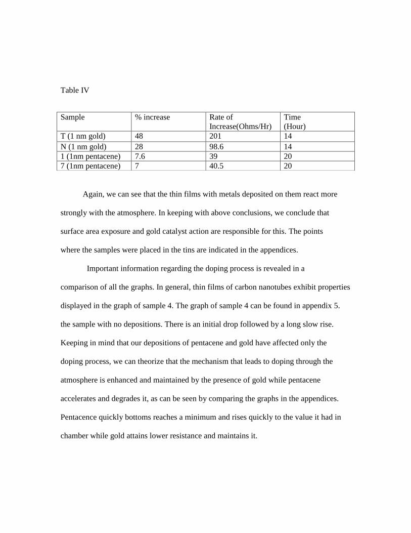
Table IV
Again, we can see that the thin films with metals deposited on them react more
strongly with the atmosphere. In keeping with above conclusions, we conclude that
surface area exposure and gold catalyst action are responsible for this. The points
where the samples were placed in the tins are indicated in the appendices.
Important information regarding the doping process is revealed in a
comparison of all the graphs. In general, thin films of carbon nanotubes exhibit properties
displayed in the graph of sample 4. The graph of sample 4 can be found in appendix 5.
the sample with no depositions. There is an initial drop followed by a long slow rise.
Keeping in mind that our depositions of pentacene and gold have affected only the
doping process, we can theorize that the mechanism that leads to doping through the
atmosphere is enhanced and maintained by the presence of gold while pentacene
accelerates and degrades it, as can be seen by comparing the graphs in the appendices.
Pentacence quickly bottoms reaches a minimum and rises quickly to the value it had in
chamber while gold attains lower resistance and maintains it.
Sample % increase Rate of
Increase(Ohms/Hr)
Time
(Hour)
T (1 nm gold) 48 201 14
N (1 nm gold) 28 98.6 14
1 (1nm pentacene) 7.6 39 20
7 (1nm pentacene) 7 40.5 20
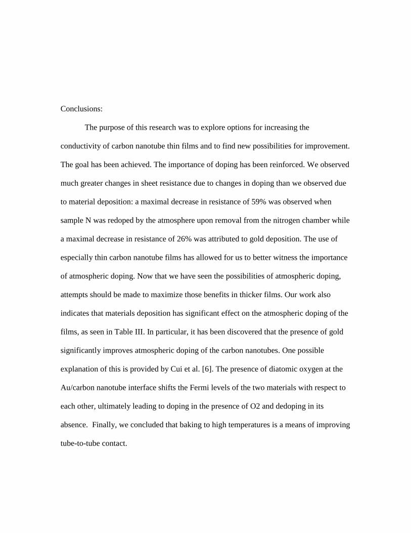
Conclusions:
The purpose of this research was to explore options for increasing the
conductivity of carbon nanotube thin films and to find new possibilities for improvement.
The goal has been achieved. The importance of doping has been reinforced. We observed
much greater changes in sheet resistance due to changes in doping than we observed due
to material deposition: a maximal decrease in resistance of 59% was observed when
sample N was redoped by the atmosphere upon removal from the nitrogen chamber while
a maximal decrease in resistance of 26% was attributed to gold deposition. The use of
especially thin carbon nanotube films has allowed for us to better witness the importance
of atmospheric doping. Now that we have seen the possibilities of atmospheric doping,
attempts should be made to maximize those benefits in thicker films. Our work also
indicates that materials deposition has significant effect on the atmospheric doping of the
films, as seen in Table III. In particular, it has been discovered that the presence of gold
significantly improves atmospheric doping of the carbon nanotubes. One possible
explanation of this is provided by Cui et al. [6]. The presence of diatomic oxygen at the
Au/carbon nanotube interface shifts the Fermi levels of the two materials with respect to
each other, ultimately leading to doping in the presence of O2 and dedoping in its
absence. Finally, we concluded that baking to high temperatures is a means of improving
tube-to-tube contact.

Acknowledgements:
Evan Donoghue and Professor Rinzler proved mentoring, support, and direction
throughout the project. Bo Liu, Mitchell McCarthy, Pooja Wadhwa, and Rajib Daas
provided much needed and appreciated tutoring.
1- Saitio , Dresselhaus, Physical Properties of Carbon Nanotubes, Imperial College Press
(1998).
2 – M. Staderman et al. Phys. Rev. B, 69, 201402 (2004).
3 – Wu et al, Science 305, 1273 (2004).
4 – Beinfat et al, Phys. Rev. 70, 035410 (2004).
5 – K. Tsukagoshi, I. Yagi, and Y. Aoyagi, Appl. Phys. Lett. 85, 1021 (2004)
6 – Xiaodong Cui, Marcus Freetag, Richard Martel, Louis Brus, and Phaedon Avouris,
Nano Letters. 3, 783 (2003).