Carbon nanotubes: opportunities and challengesdailab.stanford.edu/Reprint/46. Carbon...
24
Carbon nanotubes: opportunities and challenges Hongjie Dai * Department of Chemistry, Stanford University, Stanford, CA 94305, USA Received 14 August 2000; accepted for publication 11 July 2001 Abstract Carbon nanotubes are graphene sheets rolled-up into cylinders with diameters as small as one nanometer. Extensive work carried out worldwide in recent years has revealed the intriguing electrical and mechanical properties of these novel molecular scale wires. It is now well established that carbon nanotubes are ideal model systems for studying the physics in one-dimensional solids and have significant potential as building blocks for various practical nanoscale devices. Nanotubes have been shown to be useful for miniaturized electronic, mechanical, electromechanical, chemical and scanning probe devices and materials for macroscopic composites. Progress in nanotube growth has facilitated the fundamental study and applications of nanotubes. Gaining control over challenging nanotube growth issues is critical to the future advancement of nanotube science and technology, and is being actively pursued by researchers. Ó 2001 Elsevier Science B.V. All rights reserved. Keywords: Carbon; Chemical vapor deposition; Electrical transport measurements; Quantum effects; Chemisorption 1. Introduction A new form of carbon, buckministerfullerene C 60 was discovered in 1985 by a team headed by Smalley, Kroto and coworkers [1], and led to the Nobel Prize in chemistry in 1997. C 60 is a soccer ball-like molecule made of pure carbon atoms bonded in hexagon and pentagon configurations. Besides diamond, graphite and C 60 , quasi one- dimensional nanotube is another form of carbon first reported by Iijima in 1991 when he discovered multi-walled carbon nanotubes (MWNT) in car- bon-soot made by an arc-discharge method [2]. About two years later, he made the observation of single-walled nanotubes (SWNTs) [3]. Since then, nanotubes have captured the attention of re- searchers worldwide. A significant amount of work has been done in the past decade to reveal the unique structural, electrical, mechanical, electro- mechanical and chemical properties of carbon nanotubes and to explore what might be the key applications of these novel materials. A SWNT is a graphene sheet (Fig. 1) rolled-over into a cylinder with typical diameter on the order of 1.4 nm (Fig. 3a–d), similar to that of a C 60 bucky- ball. A MWNT consists of concentric cylinders with an interlayer spacing of 3.4 A and a diameter typically on the order of 10–20 nm (Fig. 2a–c). The lengths of the two types of tubes can be up to hundreds of microns or even centimeters. A SWNT is a molecular scale wire that has two key structural parameters. By folding a graphene sheet into a Surface Science 500 (2002) 218–241 www.elsevier.com/locate/susc * Fax: +1-650-725-0259. E-mail address: [email protected] (H. Dai). 0039-6028/01/$ - see front matter Ó 2001 Elsevier Science B.V. All rights reserved. PII:S0039-6028(01)01558-8
Transcript of Carbon nanotubes: opportunities and challengesdailab.stanford.edu/Reprint/46. Carbon...
Carbon nanotubes: opportunities and challenges
Hongjie Dai *
Department of Chemistry, Stanford University, Stanford, CA 94305, USA
Received 14 August 2000; accepted for publication 11 July 2001
Abstract
Carbon nanotubes are graphene sheets rolled-up into cylinders with diameters as small as one nanometer. Extensive
work carried out worldwide in recent years has revealed the intriguing electrical and mechanical properties of these
novel molecular scale wires. It is now well established that carbon nanotubes are ideal model systems for studying the
physics in one-dimensional solids and have significant potential as building blocks for various practical nanoscale
devices. Nanotubes have been shown to be useful for miniaturized electronic, mechanical, electromechanical, chemical
and scanning probe devices and materials for macroscopic composites. Progress in nanotube growth has facilitated the
fundamental study and applications of nanotubes. Gaining control over challenging nanotube growth issues is critical
to the future advancement of nanotube science and technology, and is being actively pursued by researchers. � 2001
Elsevier Science B.V. All rights reserved.
Keywords: Carbon; Chemical vapor deposition; Electrical transport measurements; Quantum effects; Chemisorption
1. Introduction
A new form of carbon, buckministerfullereneC60 was discovered in 1985 by a team headed bySmalley, Kroto and coworkers [1], and led to theNobel Prize in chemistry in 1997. C60 is a soccerball-like molecule made of pure carbon atomsbonded in hexagon and pentagon configurations.Besides diamond, graphite and C60, quasi one-dimensional nanotube is another form of carbonfirst reported by Iijima in 1991 when he discoveredmulti-walled carbon nanotubes (MWNT) in car-bon-soot made by an arc-discharge method [2].About two years later, he made the observation of
single-walled nanotubes (SWNTs) [3]. Since then,nanotubes have captured the attention of re-searchers worldwide. A significant amount of workhas been done in the past decade to reveal theunique structural, electrical, mechanical, electro-mechanical and chemical properties of carbonnanotubes and to explore what might be the keyapplications of these novel materials.
A SWNT is a graphene sheet (Fig. 1) rolled-overinto a cylinder with typical diameter on the order of1.4 nm (Fig. 3a–d), similar to that of a C60 bucky-ball. A MWNT consists of concentric cylinderswith an interlayer spacing of 3.4 �AA and a diametertypically on the order of 10–20 nm (Fig. 2a–c). Thelengths of the two types of tubes can be up tohundreds of microns or even centimeters. A SWNTis a molecular scale wire that has two key structuralparameters. By folding a graphene sheet into a
Surface Science 500 (2002) 218–241
www.elsevier.com/locate/susc
* Fax: +1-650-725-0259.
E-mail address: [email protected] (H. Dai).
0039-6028/01/$ - see front matter � 2001 Elsevier Science B.V. All rights reserved.
PII: S0039 -6028 (01 )01558 -8
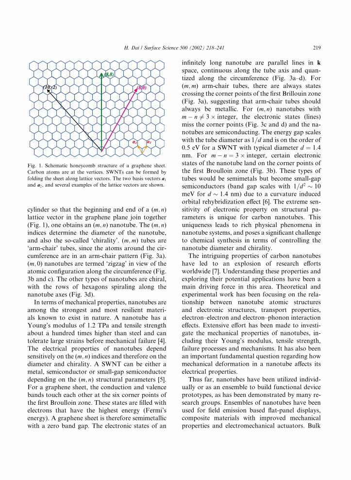
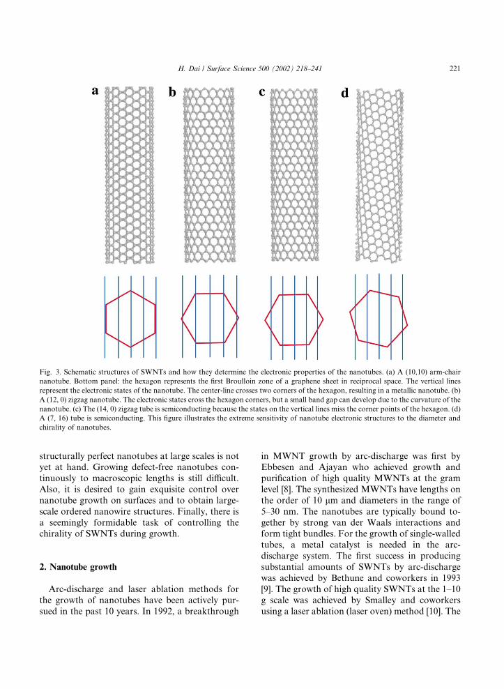
cylinder so that the beginning and end of a (m; n)lattice vector in the graphene plane join together(Fig. 1), one obtains an (m; n) nanotube. The (m; n)indices determine the diameter of the nanotube,and also the so-called ‘chirality’. (m;m) tubes are‘arm-chair’ tubes, since the atoms around the cir-cumference are in an arm-chair pattern (Fig. 3a).(m; 0) nanotubes are termed ‘zigzag’ in view of theatomic configuration along the circumference (Fig.3b and c). The other types of nanotubes are chiral,with the rows of hexagons spiraling along thenanotube axes (Fig. 3d).
In terms of mechanical properties, nanotubes areamong the strongest and most resilient materi-als known to exist in nature. A nanotube has aYoung’s modulus of 1.2 TPa and tensile strengthabout a hundred times higher than steel and cantolerate large strains before mechanical failure [4].The electrical properties of nanotubes dependsensitively on the (m; n) indices and therefore on thediameter and chirality. A SWNT can be either ametal, semiconductor or small-gap semiconductordepending on the (m; n) structural parameters [5].For a graphene sheet, the conduction and valencebands touch each other at the six corner points ofthe first Broulloin zone. These states are filled withelectrons that have the highest energy (Fermi’senergy). A graphene sheet is therefore semimetallicwith a zero band gap. The electronic states of an
infinitely long nanotube are parallel lines in k
space, continuous along the tube axis and quan-tized along the circumference (Fig. 3a–d). For(m;m) arm-chair tubes, there are always statescrossing the corner points of the first Brillouin zone(Fig. 3a), suggesting that arm-chair tubes shouldalways be metallic. For (m; n) nanotubes withm� n 6¼ 3� integer, the electronic states (lines)miss the corner points (Fig. 3c and d) and the na-notubes are semiconducting. The energy gap scaleswith the tube diameter as 1=d and is on the order of0.5 eV for a SWNT with typical diameter d ¼ 1:4nm. For m� n ¼ 3� integer, certain electronicstates of the nanotube land on the corner points ofthe first Broulloin zone (Fig. 3b). These types oftubes would be semimetals but become small-gapsemiconductors (band gap scales with 1=d2 � 10meV for d � 1:4 nm) due to a curvature inducedorbital rehybridization effect [6]. The extreme sen-sitivity of electronic property on structural pa-rameters is unique for carbon nanotubes. Thisuniqueness leads to rich physical phenomena innanotube systems, and poses a significant challengeto chemical synthesis in terms of controlling thenanotube diameter and chirality.
The intriguing properties of carbon nanotubeshave led to an explosion of research effortsworldwide [7]. Understanding these properties andexploring their potential applications have been amain driving force in this area. Theoretical andexperimental work has been focusing on the rela-tionship between nanotube atomic structuresand electronic structures, transport properties,electron–electron and electron–phonon interactioneffects. Extensive effort has been made to investi-gate the mechanical properties of nanotubes, in-cluding their Young’s modulus, tensile strength,failure processes and mechanisms. It has also beenan important fundamental question regarding howmechanical deformation in a nanotube affects itselectrical properties.
Thus far, nanotubes have been utilized individ-ually or as an ensemble to build functional deviceprototypes, as has been demonstrated by many re-search groups. Ensembles of nanotubes have beenused for field emission based flat-panel displays,composite materials with improved mechanicalproperties and electromechanical actuators. Bulk
Fig. 1. Schematic honeycomb structure of a graphene sheet.
Carbon atoms are at the vertices. SWNTs can be formed by
folding the sheet along lattice vectors. The two basis vectors a1
and a2, and several examples of the lattice vectors are shown.
H. Dai / Surface Science 500 (2002) 218–241 219
quantities of nanotubes have also been suggestedas high-capacity hydrogen storage media. Indi-vidual nanotubes have been used for field emissionsources, tips for scanning probe microscopy, nano-tweezers and chemical sensors. Nanotubes arealso promising as the central elements for futureminiaturized electronic devices.
The success in nanotube growth has led to thewide availability of nanotube materials, which is amain catalyst behind the recent leaps-and-boundsin basis physics studies and applications of na-notubes [7]. The full potential of nanotubes forapplications will not be realized until the growth ofnanotubes can be further optimized and controlled.
Real-world applications of nanotubes require ei-ther large quantities of bulk materials or deviceintegration in a scale-up fashion. For applicationssuch as composites and hydrogen storage, it isdesired to obtain high quality nanotubes at thekilogram or ton level using growth methods thatare simple, efficient and inexpensive. For devicessuch as nanotube based electronics, scale-up willunavoidably rely on self-assembly techniques orcontrolled growth strategies on surfaces combinedwith microfabrication techniques. Significant workhas been carried out to tackle these issues. Never-theless, many challenges remain in the nanotubegrowth area. An efficient growth approach to
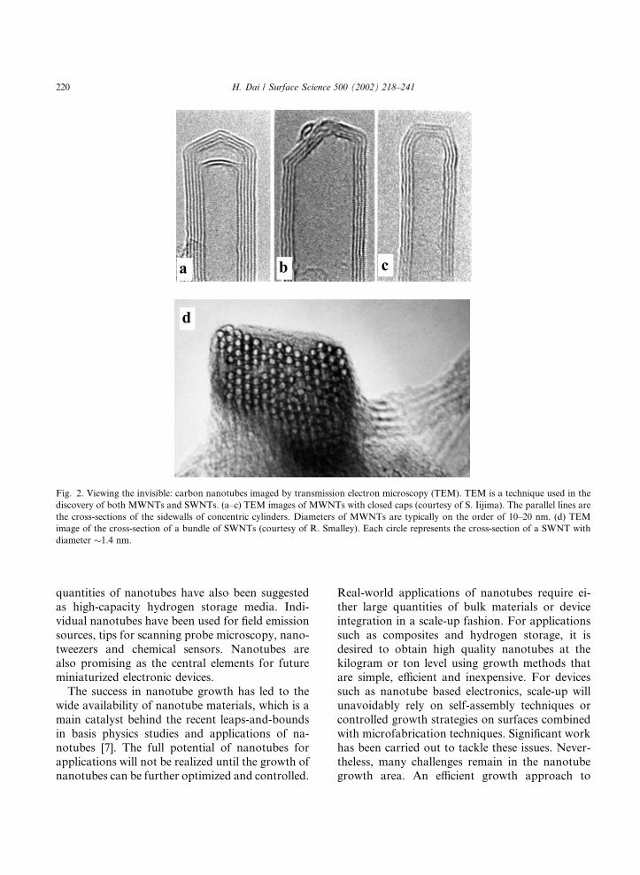
Fig. 2. Viewing the invisible: carbon nanotubes imaged by transmission electron microscopy (TEM). TEM is a technique used in the
discovery of both MWNTs and SWNTs. (a–c) TEM images of MWNTs with closed caps (courtesy of S. Iijima). The parallel lines are
the cross-sections of the sidewalls of concentric cylinders. Diameters of MWNTs are typically on the order of 10–20 nm. (d) TEM
image of the cross-section of a bundle of SWNTs (courtesy of R. Smalley). Each circle represents the cross-section of a SWNT with
diameter �1.4 nm.
220 H. Dai / Surface Science 500 (2002) 218–241
structurally perfect nanotubes at large scales is notyet at hand. Growing defect-free nanotubes con-tinuously to macroscopic lengths is still difficult.Also, it is desired to gain exquisite control overnanotube growth on surfaces and to obtain large-scale ordered nanowire structures. Finally, there isa seemingly formidable task of controlling thechirality of SWNTs during growth.
2. Nanotube growth
Arc-discharge and laser ablation methods forthe growth of nanotubes have been actively pur-sued in the past 10 years. In 1992, a breakthrough
in MWNT growth by arc-discharge was first byEbbesen and Ajayan who achieved growth andpurification of high quality MWNTs at the gramlevel [8]. The synthesized MWNTs have lengths onthe order of 10 lm and diameters in the range of5–30 nm. The nanotubes are typically bound to-gether by strong van der Waals interactions andform tight bundles. For the growth of single-walledtubes, a metal catalyst is needed in the arc-discharge system. The first success in producingsubstantial amounts of SWNTs by arc-dischargewas achieved by Bethune and coworkers in 1993[9]. The growth of high quality SWNTs at the 1–10g scale was achieved by Smalley and coworkersusing a laser ablation (laser oven) method [10]. The
Fig. 3. Schematic structures of SWNTs and how they determine the electronic properties of the nanotubes. (a) A (10,10) arm-chair
nanotube. Bottom panel: the hexagon represents the first Broulloin zone of a graphene sheet in reciprocal space. The vertical lines
represent the electronic states of the nanotube. The center-line crosses two corners of the hexagon, resulting in a metallic nanotube. (b)
A (12, 0) zigzag nanotube. The electronic states cross the hexagon corners, but a small band gap can develop due to the curvature of the
nanotube. (c) The (14, 0) zigzag tube is semiconducting because the states on the vertical lines miss the corner points of the hexagon. (d)
A (7, 16) tube is semiconducting. This figure illustrates the extreme sensitivity of nanotube electronic structures to the diameter and
chirality of nanotubes.
H. Dai / Surface Science 500 (2002) 218–241 221
produced SWNTs are mostly in the form of ropesconsisting of tens of individual nanotubes closepacked into hexagonal crystals via van der Waalsinteractions (Fig. 2d). The optimization of SWNTgrowth by arc-discharge was achieved by Journetand coworkers using a carbon anode containing1.0 at.% of yttrium and 4.2 at.% of nickel as cata-lysts [11].
Another method for producing solid state car-bon materials is chemical vapor deposition (CVD)of hydrocarbon gases. CVD methods have beensuccessful in making carbon fiber, filament andnanotube materials for more than 20 years [12–16].The growth process involves heating a catalystmaterial to high temperatures (500–1000 �C) in atube furnace, and flowing a hydrocarbon gasthrough the tube reactor over a period of time. Thecatalytic species are typically transition-metalnanoparticles that are formed on a support mate-rial such as porous aluminum oxide (alumina)materials with large surface areas. The generalnanotube growth mechanism in a CVD processinvolves the dissociation of hydrocarbon mole-cules catalyzed by the transition metal, and dis-solution and saturation of carbon atoms in themetal nanoparticle. The precipitation of carbonfrom the saturated metal particle leads to theformation of tubular carbon solids in an sp2
structure. Tubule formation is favored over otherforms of carbon such as graphitic sheets with openedges. This is due to that a tube contains nodangling bonds and therefore is in a low energyform. For MWNT growth, most of the CVDmethods employ ethylene or acetylene as the car-bon feedstock and the growth temperature is typ-ically in the range of 550–750 �C. Iron, nickel orcobalt nanoparticles are often used as catalysts.The rationale for choosing these metals as cata-lysts for CVD growth of nanotubes lies in thephase diagrams for the metals and carbon. At hightemperatures, carbon has a finite solubility in thesemetals, which leads to the formation of metal–carbon solid state solutions and therefore to theaforementioned growth mechanism.
CVD methods have great potential for scaled-upnanotube materials synthesis. Multi-walled na-notubes have already been produced commerciallyon the kilogram to ton level. Nevertheless, these
MWNTs tend to contain high densities of defectssuch as pentagons and heptagons on the sidewallsof the nanotubes. The success of nearly defect-freesingle-walled carbon nanotube growth by CVD isrelatively recent.
Our group has found that by using methane ascarbon feedstock, reaction temperatures in therange of 850–1000 �C and alumina supportedcatalyst materials, one can grow high qualitySWNT materials by CVD [17–20]. High growthtemperatures favor the formation of SWNTs thathave small diameters and thus high strain energies,and allow for nearly defect-free tube structures.Methane is the most stable hydrocarbon againstself-decomposition at high temperatures, and thecatalytic decomposition of methane by the transi-tion-metal catalyst particles is the dominant pro-cess in SWNT growth. Highly porous catalystswith strong metal–support interactions and highsurface areas produce SWNTs with better qualityat larger quantities. Strong metal–support inter-action means high metal dispersion and thus ahigh density of catalytic sites on the support. Thestrong interaction can prevent metal species fromaggregating and forming unwanted large particlesthat could yield to graphitic particles or defectivemulti-walled tubular structures in CVD. Largesurface area and a highly porous structure of thecatalyst increase the yield of SWNTs, because of ahigh density of catalytic sites owing to the formerand rapid diffusion and efficient supply of carbonfeedstock to the catalytic sites owing to the latter.
Liu and coworkers made significant progressrecently in obtaining an excellent catalyst formethane CVD growth of SWNTs [21]. The cata-lyst preparation involved supercritical drying athigh pressure and temperature conditions. Thecatalyst exhibited ultra-high surface area and po-rous structure as preserved by the supercriticaldrying condition under which destructive capillaryforces are non-existent. The catalyst yielded abun-dant SWNTs in CVD. In general, understandingthe chemistry involved in catalyst preparation andnanotube growth should lead to further break-throughs towards scale-up of the growth of perfectSWNT materials.
CVD of methane for the growth of bulk amountsof SWNTs has been investigated by Rao and
222 H. Dai / Surface Science 500 (2002) 218–241
coworkers using catalysts based on mixed oxidespinels [22]. Good quality and quantity nanotubeswere obtained with nanoparticles of a Fe–Coalloy. Colomer and coworkers recently reportedthe growth of bulk quantities of SWNTs by CVDof methane using a cobalt catalyst supported onmagnesium oxide materials [23].
It has been demonstrated that catalytic growthof SWNTs can be achieved by CVD of severaltypes of hydrocarbons and certain carbon-con-taining molecules. A CVD approach to SWNTswas developed by Smalley and coworkers whoused supported catalysts, ethylene as carbon feed-stock and growth temperature around 800 �C [24].In this case, low partial-pressure ethylene wasemployed in order to reduce amorphous carbonformation due to the self-decomposition of ethyl-ene at the high growth temperature.
Catalyst particles can be generated from the gasphase in situ for the growth of SWNTs by CVD.Cheng and coworkers reported a method thatemploys benzene as the carbon feedstock, hydro-gen as the carrier gas, and ferrocene as the catalystprecursor for SWNT growth [25]. In this method,ferrocene is vaporized and carried into a reactiontube by benzene and hydrogen gases. The reactiontube is heated at 1100–1200 �C. The vaporizedferrocene decomposes in the reactor, which leadsto the formation of iron particles that can catalyzethe growth of SWNTs. More recently, the Smalleygroup developed a gas phase catalytic process togrow bulk quantities of SWNTs [26]. Carbonmonoxide (CO) is used as the carbon feedstockand the growth temperature is in the range of 800–1200 �C. Catalytic particles for SWNT growth aregenerated in situ by thermal decomposition of ironpentacarbonyl in a reactor heated to the growthtemperature. CO provides the carbon feedstockfor the growth of nanotubes off the iron catalystparticles.
CVD and gas phase catalytic growth of na-notubes have been actively pursued in recent yearsbecause of their significant potential for materialsscale-up. With continued effort in this area, it isexpected that large quantities (up to tons) of highquality nanotube materials can be produced in thenear future.
3. Controlled nanotube growth by chemical vapor
deposition
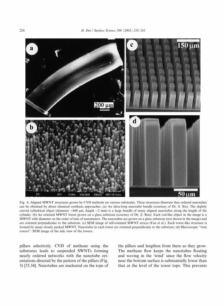
With arc-discharge or laser ablation techniques,only tangled nanotubes mixed randomly withvarious impurities are obtainable. Recent researchactivities in CVD nanotube growth have also beensparked by the idea that aligned and orderednanotube structures can be grown on surfaceswith control [17]. Xie et al. have grown alignedMWNTs out of the pores of mesoporous silica[27,28] by a CVD approach. The catalyst used isiron oxide particles embedded in the pores ofsilica. The carbon feedstock is 9% acetylene innitrogen at an overall 180 Torr pressure, and thegrowth temperature is 600 �C. Remarkably, na-notubes with lengths up to milimeters are made(Fig. 4a) [28]. Ren and coworkers have been ableto grow large-diameter MWNTs forming oriented‘forests’ (Fig. 4b) on glass substrates [29]. Plasma-assisted CVD at 660 �C is used in this work withnickel as the catalyst, and acetylene as the carbonfeedstock. Fan and coworkers have obtained or-dered MWNT structures by CVD on catalyticallypatterned substrates [30–32]. MWNTs self-assem-ble into aligned structures during CVD growth.Squared iron patterns on porous silicon substratesare employed for the growth. Regularly positionedarrays of nanotube towers are grown on the sub-strate (Fig. 4c and d). The nanotube towers exhibitvery sharp edges and corners with no nanotubesbranching away from the blocks. The MWNTswithin each block are well aligned along the di-rection perpendicular to the substrate surface [30].The mechanism of nanotube self-orientation in-volves the nanotube base-growth mode substrates[30]. During CVD growth, the outmost walls of thenanotubes interact with their neighbors via van derWaals forces to form a rigid bundle, which allowsthe nanotubes to self-orient and grow perpendic-ular to the substrate.
It is challenging to grow SWNTs into structureswith well controlled orientations. Nevertheless,suspended SWNT networks with directionality onsubstrates containing lithographically patternedsilicon pillars have been grown. Contact printing isused to transfer catalyst materials onto the tops of
H. Dai / Surface Science 500 (2002) 218–241 223
pillars selectively. CVD of methane using thesubstrates leads to suspended SWNTs formingnearly ordered networks with the nanotube ori-entations directed by the pattern of the pillars (Fig.5) [33,34]. Nanotubes are nucleated on the tops of
the pillars and lengthen from there as they grow.The methane flow keeps the nanotubes floatingand waving in the ‘wind’ since the flow velocitynear the bottom surface is substantially lower thanthat at the level of the tower tops. This prevents
Fig. 4. Aligned MWNT structures grown by CVD methods on various substrates. These structures illustrate that ordered nanotubes
can be obtained by direct chemical synthesis approaches. (a) An ultra-long nanotube bundle (courtesy of Dr. S. Xie). The slightly
curved cylindrical object (diameter �600 lm, length �2 mm) is a large bundle of many aligned nanotubes along the length of the
cylinder. (b) An oriented MWNT forest grown on a glass substrate (courtesy of Dr. Z. Ren). Each rod-like object in the image is a
MWNT with diameter on the order of tens of nanometers. The nanotubes are grown on a glass substrate (not shown in the image) and
are oriented perpendicular to the substrate. (c) SEM image of self-oriented MWNT arrays (Fan et al.). Each tower-like structure is
formed by many closely packed MWNT. Nanotubes in each tower are oriented perpendicular to the substrate. (d) Microscopic ‘‘twin
towers’’: SEM image of the side view of the towers.
224 H. Dai / Surface Science 500 (2002) 218–241
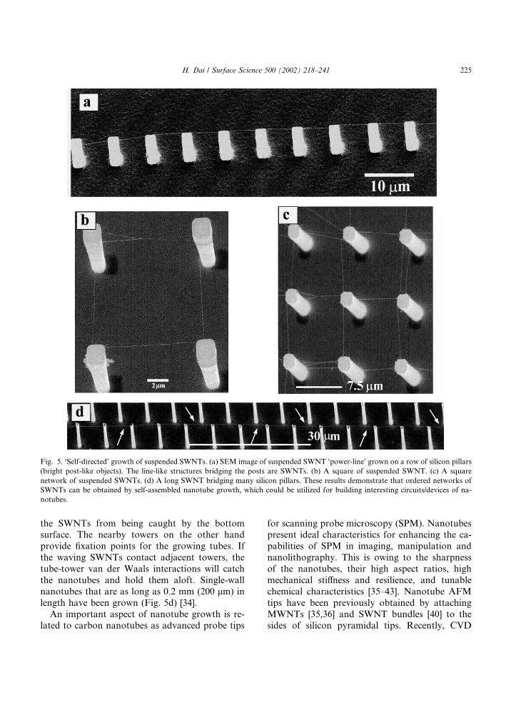
the SWNTs from being caught by the bottomsurface. The nearby towers on the other handprovide fixation points for the growing tubes. Ifthe waving SWNTs contact adjacent towers, thetube-tower van der Waals interactions will catchthe nanotubes and hold them aloft. Single-wallnanotubes that are as long as 0.2 mm (200 lm) inlength have been grown (Fig. 5d) [34].
An important aspect of nanotube growth is re-lated to carbon nanotubes as advanced probe tips
for scanning probe microscopy (SPM). Nanotubespresent ideal characteristics for enhancing the ca-pabilities of SPM in imaging, manipulation andnanolithography. This is owing to the sharpnessof the nanotubes, their high aspect ratios, highmechanical stiffness and resilience, and tunablechemical characteristics [35–43]. Nanotube AFMtips have been previously obtained by attachingMWNTs [35,36] and SWNT bundles [40] to thesides of silicon pyramidal tips. Recently, CVD
Fig. 5. ‘Self-directed’ growth of suspended SWNTs. (a) SEM image of suspended SWNT ‘power-line’ grown on a row of silicon pillars
(bright post-like objects). The line-like structures bridging the posts are SWNTs. (b) A square of suspended SWNT. (c) A square
network of suspended SWNTs. (d) A long SWNT bridging many silicon pillars. These results demonstrate that ordered networks of
SWNTs can be obtained by self-assembled nanotube growth, which could be utilized for building interesting circuits/devices of na-
notubes.
H. Dai / Surface Science 500 (2002) 218–241 225
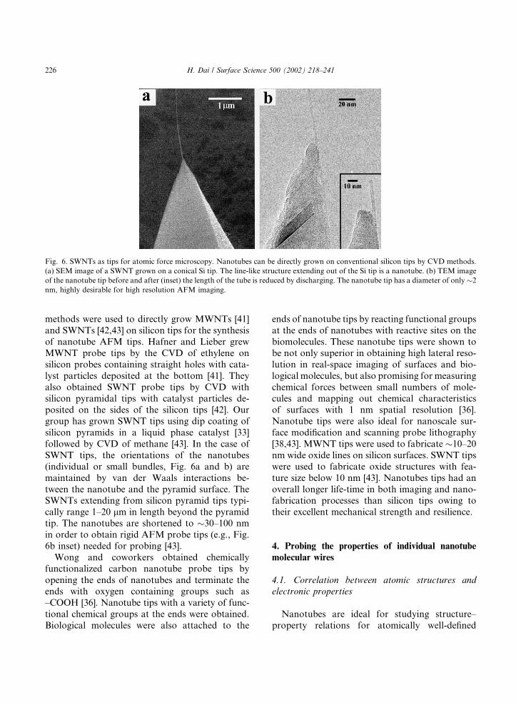
methods were used to directly grow MWNTs [41]and SWNTs [42,43] on silicon tips for the synthesisof nanotube AFM tips. Hafner and Lieber grewMWNT probe tips by the CVD of ethylene onsilicon probes containing straight holes with cata-lyst particles deposited at the bottom [41]. Theyalso obtained SWNT probe tips by CVD withsilicon pyramidal tips with catalyst particles de-posited on the sides of the silicon tips [42]. Ourgroup has grown SWNT tips using dip coating ofsilicon pyramids in a liquid phase catalyst [33]followed by CVD of methane [43]. In the case ofSWNT tips, the orientations of the nanotubes(individual or small bundles, Fig. 6a and b) aremaintained by van der Waals interactions be-tween the nanotube and the pyramid surface. TheSWNTs extending from silicon pyramid tips typi-cally range 1–20 lm in length beyond the pyramidtip. The nanotubes are shortened to �30–100 nmin order to obtain rigid AFM probe tips (e.g., Fig.6b inset) needed for probing [43].
Wong and coworkers obtained chemicallyfunctionalized carbon nanotube probe tips byopening the ends of nanotubes and terminate theends with oxygen containing groups such as–COOH [36]. Nanotube tips with a variety of func-tional chemical groups at the ends were obtained.Biological molecules were also attached to the
ends of nanotube tips by reacting functional groupsat the ends of nanotubes with reactive sites on thebiomolecules. These nanotube tips were shown tobe not only superior in obtaining high lateral reso-lution in real-space imaging of surfaces and bio-logical molecules, but also promising for measuringchemical forces between small numbers of mole-cules and mapping out chemical characteristicsof surfaces with 1 nm spatial resolution [36].Nanotube tips were also ideal for nanoscale sur-face modification and scanning probe lithography[38,43]. MWNT tips were used to fabricate �10–20nm wide oxide lines on silicon surfaces. SWNT tipswere used to fabricate oxide structures with fea-ture size below 10 nm [43]. Nanotubes tips had anoverall longer life-time in both imaging and nano-fabrication processes than silicon tips owing totheir excellent mechanical strength and resilience.
4. Probing the properties of individual nanotube
molecular wires
4.1. Correlation between atomic structures andelectronic properties
Nanotubes are ideal for studying structure–property relations for atomically well-defined
Fig. 6. SWNTs as tips for atomic force microscopy. Nanotubes can be directly grown on conventional silicon tips by CVD methods.
(a) SEM image of a SWNT grown on a conical Si tip. The line-like structure extending out of the Si tip is a nanotube. (b) TEM image
of the nanotube tip before and after (inset) the length of the tube is reduced by discharging. The nanotube tip has a diameter of only �2
nm, highly desirable for high resolution AFM imaging.
226 H. Dai / Surface Science 500 (2002) 218–241
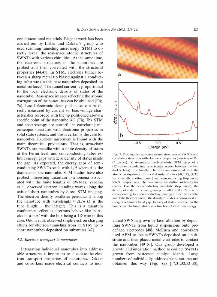
one-dimensional materials. Elegant work has beencarried out by Lieber and Dekker’s group whoused scanning tunneling microscopy (STM) to di-rectly reveal the real-space atomic structures ofSWNTs with various chiralities. At the same time,the electronic structures of the nanotubes areprobed and then correlated with the structuralproperties [44,45]. In STM, electrons tunnel be-tween a sharp metal tip biased against a conduct-ing substrate (in this case nanotubes deposited onmetal surfaces). The tunnel current is proportionalto the local electronic density of states of thenanotube. Real-space images reflecting the atomiccorrugation of the nanotubes can be obtained (Fig.7a). Local electronic density of states can be di-rectly measured by current vs. bias-voltage char-acteristics recorded with the tip positioned above aspecific point of the nanotube [46] (Fig. 7b). STMand spectroscopy are powerful in correlating mi-croscopic structures with electronic properties insolid state systems, and this is certainly the case fornanotubes. Excellent agreement is found with themain theoretical predictions. That is, arm-chairSWNTs are metallic with a finite density of statesat the Fermi level, and semiconducting tubes ex-hibit energy gaps with zero density of states insidethe gap. As expected, the energy gaps of semi-conducting SWNTs scale with 1=d where d is thediameter of the nanotube. STM studies have alsoprobed interesting quantum phenomena associ-ated with the finite lengths of SWNTs. Venemaet al. observed electron standing waves along theaxis of short nanotubes by direct STM imaging.The electron density oscillates periodically alongthe nanotube with wavelength � 2L=n (L is thetube length, n the integer). This is a quantumconfinement effect as electrons behave like ‘parti-cles-in-a-box’ with the box being a 1D wire in thiscase. Odom et al. observed single electron chargingeffects for electron tunneling from an STM tip toshort nanotubes deposited on substrates [47].
4.2. Electron transport in nanotubes
Integrating individual nanotubes into address-able structures is important to elucidate the elec-tron transport properties of nanotubes. Dekkerand coworkers made electrical contacts to indi-
vidual SWNTs grown by laser ablation by depos-iting SWNTs from liquid suspensions onto pre-defined electrodes [48]. McEuen and coworkersused AFM to locate SWNTs deposited on a sub-strate and then placed metal electrodes to contactthe nanotubes [49–51]. Our group developed agrowth and integration method to contact SWNTsgrown from patterned catalyst islands. Largenumbers of individually addressable nanotubes areobtained this way (Fig. 8a) [17,31,32,52–58].
Fig. 7. Probing the real-space atomic structures of SWNTs and
correlating structures with electronic properties (courtesy of Dr.
C. Lieber). (a) Atomically resolved (dots) STM image of a
(12,�2) semiconducting tube (center region between the two
darker lines) in a bundle. The dots are associated with the
atomic corrugations. (b) Local density of states ðdI=dV Þ=ðI=V Þfor a metallic (bottom curve) and semiconducting (top curve)
SWNT respectively. The two curves are shifted artificially for
clarity. For the semiconducting nanotube (top curve), the
density of state in the energy range of �0.2 to 0.2 eV is zero,
corresponding to a semiconducting band gap. For the metallic
nanotube (bottom curve), the density of states is non-zero at all
energies without a band gap. Density of states is defined as the
number of electronic states as a function of electronic energy.
H. Dai / Surface Science 500 (2002) 218–241 227
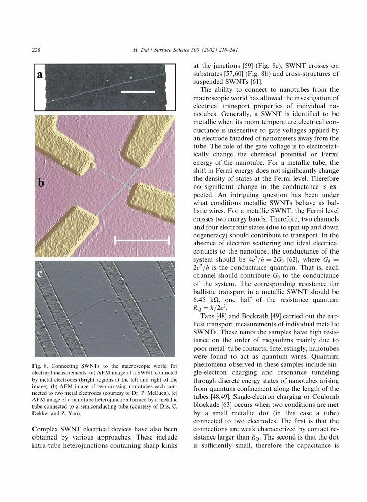
Complex SWNT electrical devices have also beenobtained by various approaches. These includeintra-tube heterojunctions containing sharp kinks
at the junctions [59] (Fig. 8c), SWNT crosses onsubstrates [57,60] (Fig. 8b) and cross-structures ofsuspended SWNTs [61].
The ability to connect to nanotubes from themacroscopic world has allowed the investigation ofelectrical transport properties of individual na-notubes. Generally, a SWNT is identified to bemetallic when its room temperature electrical con-ductance is insensitive to gate voltages applied byan electrode hundred of nanometers away from thetube. The role of the gate voltage is to electrostat-ically change the chemical potential or Fermienergy of the nanotube. For a metallic tube, theshift in Fermi energy does not significantly changethe density of states at the Fermi level. Thereforeno significant change in the conductance is ex-pected. An intriguing question has been underwhat conditions metallic SWNTs behave as bal-listic wires. For a metallic SWNT, the Fermi levelcrosses two energy bands. Therefore, two channelsand four electronic states (due to spin up and downdegeneracy) should contribute to transport. In theabsence of electron scattering and ideal electricalcontacts to the nanotube, the conductance of thesystem should be 4e2=h ¼ 2G0 [62], where G0 ¼2e2=h is the conductance quantum. That is, eachchannel should contribute G0 to the conductanceof the system. The corresponding resistance forballistic transport in a metallic SWNT should be6.45 kX, one half of the resistance quantumRQ ¼ h=2e2.
Tans [48] and Bockrath [49] carried out the ear-liest transport measurements of individual metallicSWNTs. These nanotube samples have high resis-tance on the order of megaohms mainly due topoor metal–tube contacts. Interestingly, nanotubeswere found to act as quantum wires. Quantumphenomena observed in these samples include sin-gle-electron charging and resonance tunnelingthrough discrete energy states of nanotubes arisingfrom quantum confinement along the length of thetubes [48,49]. Single-electron charging or Coulombblockade [63] occurs when two conditions are metby a small metallic dot (in this case a tube)connected to two electrodes. The first is that theconnections are weak characterized by contact re-sistance larger than RQ. The second is that the dotis sufficiently small, therefore the capacitance is
Fig. 8. Connecting SWNTs to the macroscopic world for
electrical measurements. (a) AFM image of a SWNT contacted
by metal electrodes (bright regions at the left and right of the
image). (b) AFM image of two crossing nanotubes each con-
nected to two metal electrodes (courtesy of Dr. P. McEuen). (c)
AFM image of a nanotube heterojunction formed by a metallic
tube connected to a semiconducting tube (courtesy of Drs. C.
Dekker and Z. Yao).
228 H. Dai / Surface Science 500 (2002) 218–241
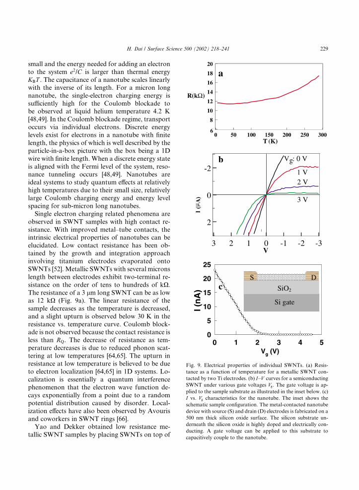
small and the energy needed for adding an electronto the system e2/C is larger than thermal energyKBT . The capacitance of a nanotube scales linearlywith the inverse of its length. For a micron longnanotube, the single-electron charging energy issufficiently high for the Coulomb blockade tobe observed at liquid helium temperature 4.2 K[48,49]. In the Coulomb blockade regime, transportoccurs via individual electrons. Discrete energylevels exist for electrons in a nanotube with finitelength, the physics of which is well described by theparticle-in-a-box picture with the box being a 1Dwire with finite length. When a discrete energy stateis aligned with the Fermi level of the system, reso-nance tunneling occurs [48,49]. Nanotubes areideal systems to study quantum effects at relativelyhigh temperatures due to their small size, relativelylarge Coulomb charging energy and energy levelspacing for sub-micron long nanotubes.
Single electron charging related phenomena areobserved in SWNT samples with high contact re-sistance. With improved metal–tube contacts, theintrinsic electrical properties of nanotubes can beelucidated. Low contact resistance has been ob-tained by the growth and integration approachinvolving titanium electrodes evaporated ontoSWNTs [52]. Metallic SWNTs with several micronslength between electrodes exhibit two-terminal re-sistance on the order of tens to hundreds of kX.The resistance of a 3 lm long SWNT can be as lowas 12 kX (Fig. 9a). The linear resistance of thesample decreases as the temperature is decreased,and a slight upturn is observed below 30 K in theresistance vs. temperature curve. Coulomb block-ade is not observed because the contact resistance isless than RQ. The decrease of resistance as tem-perature decreases is due to reduced phonon scat-tering at low temperatures [64,65]. The upturn inresistance at low temperature is believed to be dueto electron localization [64,65] in 1D systems. Lo-calization is essentially a quantum interferencephenomenon that the electron wave function de-cays exponentially from a point due to a randompotential distribution caused by disorder. Local-ization effects have also been observed by Avourisand coworkers in SWNT rings [66].
Yao and Dekker obtained low resistance me-tallic SWNT samples by placing SWNTs on top of
Fig. 9. Electrical properties of individual SWNTs. (a) Resis-
tance as a function of temperature for a metallic SWNT con-
tacted by two Ti electrodes. (b) I–V curves for a semiconducting
SWNT under various gate voltages Vg. The gate voltage is ap-
plied to the sample substrate as illustrated in the inset below. (c)
I vs. Vg characteristics for the nanotube. The inset shows the
schematic sample configuration. The metal-contacted nanotube
device with source (S) and drain (D) electrodes is fabricated on a
500 nm thick silicon oxide surface. The silicon substrate un-
derneath the silicon oxide is highly doped and electrically con-
ducting. A gate voltage can be applied to this substrate to
capacitively couple to the nanotube.
H. Dai / Surface Science 500 (2002) 218–241 229
flat gold electrodes and measured a resistance onthe order of 15 kX [67]. Bachtold and coworkersused electrostatic AFM to map out the voltagedrop across metallic SWNTs and found that thevoltage drop along the length of the nanotube isvery small [68]. These results all point to ballistictransport with minimum electron scattering inmetallic SWNTs.
Tans et al. [69], Martel et al. [70] and Zhouet al. [54] carried out measurements of individualsemiconducting SWNTs. These nanotubes exhibittransistor behavior at room temperature, that is,their conductance can be changed dramatically (byorders of magnitude) by gate voltages (Fig. 9b).The nanotubes appeared to be doped with holes asp-type. Positive gate voltages caused the Fermilevel shifting away from the valence band into theband gap, depleted the holes and turned the sys-tem into insulating states. p-type transistor behav-ior was observed consistently in semiconductingSWNTs by a number of groups. Hole doping ofSWNTs is attributed to adsorbed oxygen [71].With good metal–tube contacts, low resistancesemiconducting SWNT samples on the order ofhundreds of kiloohms were obtained by Zhouet al. [54]. The transconductance (ratio of currentchange over gate-voltage change) of these semi-conducting tube samples can be up to �200 nA/V[54], two orders of magnitude higher than mea-sured in high resistance samples. The high trans-conductance is a direct result of low sampleresistance, since high currents can be transportedthrough the system at relatively low bias voltages.This result is important since high transconduc-tance and voltage gain is essential to the perfor-mance of transistors.
McEuen and coworkers studied the electricalproperties of crosses of SWNTs [60]. Electrontransport from metallic to metallic, metallic tosemiconducting, and semiconducting to semicon-ducting tubes were investigated. The conductanceof the metal–metal tube junction was found to be�0.1 e2/h, suggesting appreciable electron scatter-ing at the crosses. Metallic and semiconductingtubes were found to form Schottky junctions at thecrosses. A Schottky junction is typically formed atthe interface between a bulk semiconductor anda pure metal. The difference in workfunction be-
tween the two materials causes energy band bend-ing in the semiconductor side. Characteristic of aSchottky junction is rectifying behavior in the cur-rent vs. voltage curves [60]. Current flows acrossthe junction only when the metal side is negativelybiased. Tombler et al. studied SWNT crosses andused scanning probes as gates to identify the metal-lic or semiconducting nature of the crossing nano-tubes [57].
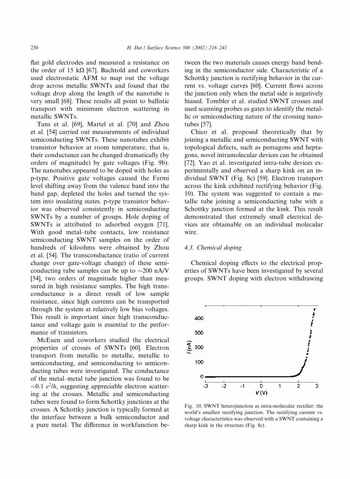
Chico et al. proposed theoretically that byjoining a metallic and semiconducting SWNT withtopological defects, such as pentagons and hepta-gons, novel intramolecular devices can be obtained[72]. Yao et al. investigated intra-tube devices ex-perimentally and observed a sharp kink on an in-dividual SWNT (Fig. 8c) [59]. Electron transportacross the kink exhibited rectifying behavior (Fig.10). The system was suggested to contain a me-tallic tube joining a semiconducting tube with aSchottky junction formed at the kink. This resultdemonstrated that extremely small electrical de-vices are obtainable on an individual molecularwire.
4.3. Chemical doping
Chemical doping effects to the electrical prop-erties of SWNTs have been investigated by severalgroups. SWNT doping with electron withdrawing
Fig. 10. SWNT heterojunction as intra-molecular rectifier: the
world’s smallest rectifying junction. The rectifying current vs.
voltage characteristics was observed with a SWNT containing a
sharp kink in the structure (Fig. 8c).
230 H. Dai / Surface Science 500 (2002) 218–241
(Br2, I2) and donating species (K, Cs) were firstcarried out with bulk SWNT mats by Lee et al.and Grigorian et al. [73,74]. Bundles of SWNTswere also studied [75,76]. With bulk mats, chemi-cal doping can lead to orders of magnitude re-duction in the resistance of bulk SWNT materialsdue to the increase in the average of hole or elec-tron carriers in the nanotubes. The doping speciesabsorb on to nanotube surfaces and intercalateinto the empty space of bundles of SWNTs [73,74].
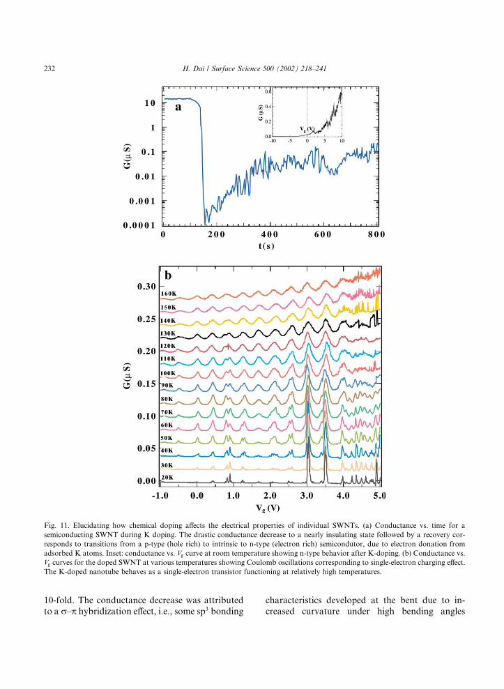
It is necessary to investigate individual SWNTssince doping effects in metallic and semiconductingSWNTs can be drastically different. Bockrath et al.carried out potassium doping of a semiconductingSWNT at room temperature. A transition from p-type to n-type was observed as K atoms absorbonto the outer surface of the nanotube and donateelectrons to the tube [76]. Similar phenomenon wasobserved by Kong et al. [77]. Fig. 11a shows theevolution of the conductance as a function of timeduring K-doping for a diameter �2.5 nm andlength ¼ 0:4 lm SWNT contacted by Ti elec-trodes. The conductance decreased dramaticallyby five orders of magnitude and then recovered.This corresponds to the nanotube evolving from p-type to intrinsic and then to n-type semiconductingstates under progressive K-doping.
More can be learned about K-doping of singletubes by characterizing the doped nanotubes atlow temperatures. Temperature dependent mea-surements of K-doped SWNTs reveal Coulombblockade [63] oscillations at high temperatures upto 160 K (Fig. 11b). The Coulomb oscillation peaksin gate voltage (Vg) is periodic and evenly spaced atDVg � 0:45 V in regime I of Fig. 11b, where eachpeak corresponds to charging and transporting oneelectron through the system. In regime II, the os-cillations are periodic with DVg � 0:45 V at hightemperatures but some of the peaks split intodoublets at low temperatures (T < 110 K). In re-gime III, periodic oscillations are observed only atT < 90 K with a small period of DVg � 0:15 V.These peaks show no splitting down to 20 K. Thechange of DVg by �0.45 V causes one electron ad-dition or removal from the dot, the gate capaci-tance is therefore Cg ¼ e=DVg ¼ 0:35 aF. The totalcapacitance of the system is estimated to beCR ¼ 3:72 aF, corresponding to a charging energy
of U ¼ e2=CR ¼ 43 meV. For charging energyU � 50 meV, the size of the quantum dot seen inregime I appears smaller than the tube length L ¼0:4 lm between the edges of metal electrodes. Thedot in regime I has an effective length of Leff �0:1–0:15 lm, about one third of the actual geo-metry of the nanotube. This phenomenon is attri-buted by an inhomogeneous K-doping profilealong the nanotube, as a result of the randomnessof K-evaporation onto the sample. That is, an in-homogeneous effect can lead to a high temperatureSET due to the formation of a single quantum dotwith its size smaller than the geometrical tubelength. This can occur when the two barriers for thedot are located within the length of the tube whilethe rest of the system is well coupled to the metalcontacts. This suggests that to obtain high tem-perature nanotube SETs reliably, it is desired toobtain samples with 10–50 nm tube lengths andhave great chemical homogeneity along the lengths.
Single-electron transistors operating at roomtemperatures have been pursued actively with Siand metal systems [78–82]. Nanotubes are poten-tial candidates for high performance SETs. Withnanotubes, room temperature single-electron charg-ing will require a tube ‘dot’ with length on the orderof 10–50 nm, so that charging energy can beU P 100 meV� 4 KBT (300 K). Room temperaturenanotube SETs could be realized in the near future.
4.4. Nanotube electromechanical properties
The question of how mechanical deformationaffects the electrical properties of carbon nanotubeshas been under theoretical and experimental stud-ies due to the potential application of nanotubesfor nanoscale electro-mechanical (NEMs) devices.The effects of mechanical deformation to the elec-trical properties of nanotubes were studied theo-retically by several groups. Nardelli and coworkersmodeled the bending of an arm-chair metallicSWNT and calculated the electrical conductancevs. bending angle [83–85]. The nanotube conduc-tance was found to change only slightly undersmall bending angles. Rochefort et al. carried outsimulations of nanotube bending and found that atlarger bending angles �45�, the electrical conduc-tance of a metallic SWNT can be lowered by up to
H. Dai / Surface Science 500 (2002) 218–241 231
10-fold. The conductance decrease was attributedto a r–p hybridization effect, i.e., some sp3 bonding
characteristics developed at the bent due to in-creased curvature under high bending angles
Fig. 11. Elucidating how chemical doping affects the electrical properties of individual SWNTs. (a) Conductance vs. time for a
semiconducting SWNT during K doping. The drastic conductance decrease to a nearly insulating state followed by a recovery cor-
responds to transitions from a p-type (hole rich) to intrinsic to n-type (electron rich) semicondutor, due to electron donation from
adsorbed K atoms. Inset: conductance vs. Vg curve at room temperature showing n-type behavior after K-doping. (b) Conductance vs.
Vg curves for the doped SWNT at various temperatures showing Coulomb oscillations corresponding to single-electron charging effect.
The K-doped nanotube behaves as a single-electron transistor functioning at relatively high temperatures.
232 H. Dai / Surface Science 500 (2002) 218–241
[84,85]. The sp3 atomic structure causes the elec-trons to be localized and is responsible for the re-duced nanotube conductance.
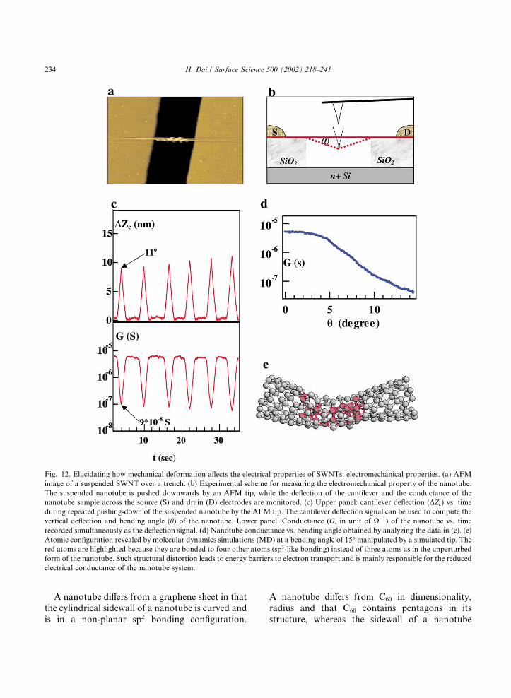
Experimental investigation of the electrome-chanical properties of nanotubes can be carried outwith suspended nanotubes, as shown by Tombleret al. [58]. A nanotube can be grown from pat-terned catalyst sites across pre-fabricated trencheson SiO2/Si substrates [58]. This leads to an indi-vidual SWNT that is partially suspended over thetrenches (Fig. 12a). The suspended part of thenanotube can be manipulated with an AFM tip,while the resistance of the sample is being moni-tored (Fig. 12b). The nanotube conductance de-creases each time the AFM tip pushes the nanotubedown, but recovers as the tip retracts (Fig. 12c).The full reversibility of the nanotube electricalconductance upon tip retraction suggests that themetal–tube contacts are not affected each timewhen the tip deflects the suspended part of thenanotube. The observed change in sample con-ductance is entirely due to the mechanical defor-mation of the SWNT caused by the pushing tip.
The conductance is found to decrease by afactor of 2 at �5� bending angle (strain �0.3%),but decreases more dramatically by two orders ofmagnitude at a bending angle �14� (strain �3%,Fig. 12d) [58]. Wu and coworkers have carried outorder-N non-orthogonal tight-binding molecular-dynamics simulations of a tip deflecting a metallic(5,5) SWNT, with the tip modeled by a short andstiff (5,5) SWNT cap [58,86]. At relatively smallbending angles, the nanotube is found to retain sp2
bonding throughout its structure, but exhibitssignificant bond distortion for the atoms in theregion near the tip. As tip-pushing and bendingproceed, the nanotube structure progressivelyevolves and larger structural changes occur in thenanotube region in the vicinity of the tip. At a 15�bending angle, the average number of bonds peratom in this region is found to increase to �3.6,suggesting the appearance of sp3-bonded atoms(marked in red in Fig. 12e). This causes a signifi-cant decrease in the local p-electron density asrevealed by electronic structure calculations. Sincethe p-electrons are delocalized and responsiblefor electrical conduction, a drastic reduction in thep-electron density is responsible for the significant
decrease in conductance. Simulations find that thelarge local sp3 deformation is highly energetic, andits appearance is entirely due to the forcing tip.The structure is found to fully reverse to sp2 uponmoving the tip away in the simulation. The com-bined experimental and theoretical study leads toan in-depth understanding of nanotube electro-mechanical properties, and suggests that SWNTscould serve as reversible electro-mechanical trans-ducers that are potentially useful for NEMs de-vices.
5. Surface science in nanotubes
5.1. Metal–nanotube interactions
The interactions between nanotubes and variousmetals are important to low resistance ohmic con-tacts to nanotubes and other issues such as formingmetal or superconducting nanowires on nanotubetemplates [87–89]. Experimental and theoreticalinvestigations of the interactions between metalsand various carbon materials have been carried outpreviously. It is known that in three-dimensionalbulk materials, different metals exhibit differentinteractions with carbon. The ability for transitionmetals to bond with carbon atoms increases withthe number of unfilled d-orbitals. Metals such asAl, Au and Pd have no d-vacancies and negligibleaffinity for carbon. Metals with few d-vacanciessuch as Ni, Fe and Co exhibit finite solubility forcarbon in certain temperature ranges. 3d and 4dmetals with many d-vacancies such as Ti and Nbcan form strong chemical bonds with carbonand thus highly stable carbide compounds. It isgenerally believed that the interactions betweendeposited metals and a graphite basal plane areweak [90–99]. The interactions are suggested to bethrough van der Waals forces and do not involvechemical bond formations between the metal andcarbon atoms in the graphite basal plane. For C60
[100–102], it has been shown that certain metalsinteract much more strongly with C60 than graphiteincluding Ti and Ni [100,102]. Deposition of Tion C60 can lead to the formation of Ti–C carbidebonds as revealed by X-ray photoelectron spec-troscopy [100].
H. Dai / Surface Science 500 (2002) 218–241 233
A nanotube differs from a graphene sheet in thatthe cylindrical sidewall of a nanotube is curved andis in a non-planar sp2 bonding configuration.
A nanotube differs from C60 in dimensionality,radius and that C60 contains pentagons in itsstructure, whereas the sidewall of a nanotube
Fig. 12. Elucidating how mechanical deformation affects the electrical properties of SWNTs: electromechanical properties. (a) AFM
image of a suspended SWNT over a trench. (b) Experimental scheme for measuring the electromechanical property of the nanotube.
The suspended nanotube is pushed downwards by an AFM tip, while the deflection of the cantilever and the conductance of the
nanotube sample across the source (S) and drain (D) electrodes are monitored. (c) Upper panel: cantilever deflection (DZc) vs. time
during repeated pushing-down of the suspended nanotube by the AFM tip. The cantilever deflection signal can be used to compute the
vertical deflection and bending angle (h) of the nanotube. Lower panel: Conductance (G, in unit of X�1) of the nanotube vs. time
recorded simultaneously as the deflection signal. (d) Nanotube conductance vs. bending angle obtained by analyzing the data in (c). (e)
Atomic configuration revealed by molecular dynamics simulations (MD) at a bending angle of 15� manipulated by a simulated tip. The
red atoms are highlighted because they are bonded to four other atoms (sp3-like bonding) instead of three atoms as in the unperturbed
form of the nanotube. Such structural distortion leads to energy barriers to electron transport and is mainly responsible for the reduced
electrical conductance of the nanotube system.
234 H. Dai / Surface Science 500 (2002) 218–241
contains exclusively hexagons. C60 therefore isexpected to be more reactive with metals than ananotube because of the pentagons in the structure.A recent theoretical study by Menon et al. shedsome light into metal–tube interactions [103]. Theyused a tight-binding molecular-dynamics methodto calculate bonding configurations of Ni with thesidewall atoms on a SWNT, and compared theresults with Ni bonding on a graphene sheet. Co-valent bonding characteristics of Ni (on certainsites) with carbon atoms on the nanotube wereidentified from the calculations. The interactionwas found to be stronger than ionic-like (chargetransfer) bonding with a graphene sheet. Thestrong Ni-SWNT interaction was attributed tocurvature-induced rehybridization of carbon sp2
orbitals with the Ni d-orbital [103].An experimental investigation of metal–tube
interaction was carried out recently by Zhanget al. by studying the structures of various metalsformed on suspended SWNTs deposited by elec-tron beam evaporation [104]. 5 nm of Ti, Ni, Pd,Au, Al, and Pb are evaporated to coat suspendedSWNTs and drastically different coating re-sults are observed (Fig. 13). Ti forms continuousnanowires on suspended SWNTs (Fig. 13a). Niand Pd form quasi-continuous and uniform coat-ings on SWNTs (Fig. 13b and c respectively), withthe wire structures occasionally disconnectedalong the lengths. Au, Al, and Pb deposited on thenanotubes form disconnected crystalline particles,leaving sections of the nanotubes free of metalcoating (Fig. 13d, e and f respectively). The Auparticles decorating SWNTs are up to �60 nmwide, much larger than the deposited film thick-ness. This indicates that Au atoms deposited onthe tubes have migrated and merged together toform large particles.
The continuous and uniform Ti coating on na-notubes suggests a high nucleation density andstrong Ti–SWNT interaction. On the contrary, theAu and Al coatings are highly discontinuous witha very low nucleation density due to weak Au,Al–SWNT interactions. A low Au-tube bindingenergy points to a low activation barrier for ad-atom diffusion. Rapid motion of Au atoms on thenanotube sidewall can cause the atoms or evensmall clusters to merge into isolated large particles
[98]. Ti atoms deposited on nanotubes exhibit thehighest condensation/sticking coefficient amongNi and other metals. The Ti–SWNT interactionshould be stronger than that for Ni–SWNT andcould involve covalent bonding due to the highaffinity of Ti for carbide formation and the cur-vature induced rehybridization effect. The intimateTi–SWNT interaction and the fact that Ti–C ishighly conducting are consistent with the resultthat low resistance ohmic electrical contacts toindividual SWNTs can be reliably made by de-positing Ti electrodes onto nanotubes [52]. It wasfound previously that Ti also makes ohmic con-tacts to doped diamonds. In this case, as depositedTi forms carbide bonds with the very surface ofdiamond, and ohmic contacts are obtained bythermal annealing that leads to a layer of carbideat the Ti–diamond interface [105].
5.2. Interactions with small molecules: nanotubechemical sensors
How molecules interact with carbon nanotubesand affect their physical properties is of funda-mental interest, and may have important implica-tions to their applications. The electrical propertiesof metallic SWNTs are relatively insensitive totheir chemical environment and interactions withother species. For an example, potassium dopingof a metallic SWNT does not affect its conduc-tance significantly [106], because the band shift dueto charge-transfer interactions does not change thedensity of states at the Fermi level for a metallictube. Semiconducting SWNTs, on the other hand,are very sensitive to K-doping, and can changefrom p-type to n-type accompanied by orders ofmagnitude change in conductance as discussedearlier. Semiconducting SWNTs are also verysensitive to gas molecule adsorption, exhibitingsignificant changes in their electrical conductance.
Colins et al. [71] have studied molecular oxygenadsorption on carbon nanotubes. The electricalproperties of nanotubes are found to be highlysensitive to oxygen adsorption effects. In a vacuumchamber, the conductance of bulk SWNTs in-creases when oxygen is introduced into the systemand recovers when vacuum is restored. Full de-sorption of oxygen can occur when heating the
H. Dai / Surface Science 500 (2002) 218–241 235
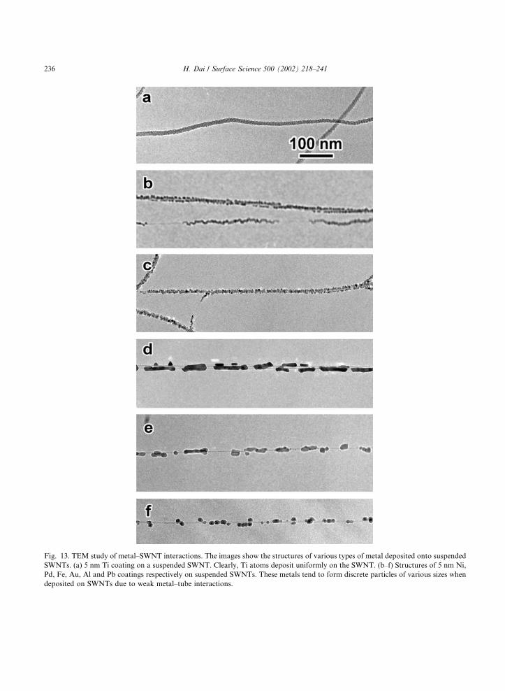
Fig. 13. TEM study of metal–SWNT interactions. The images show the structures of various types of metal deposited onto suspended
SWNTs. (a) 5 nm Ti coating on a suspended SWNT. Clearly, Ti atoms deposit uniformly on the SWNT. (b–f) Structures of 5 nm Ni,
Pd, Fe, Au, Al and Pb coatings respectively on suspended SWNTs. These metals tend to form discrete particles of various sizes when
deposited on SWNTs due to weak metal–tube interactions.
236 H. Dai / Surface Science 500 (2002) 218–241
nanotubes to high temperatures in vacuum. Co-hen’s group carried out density-functional theory(DFT) calculations on oxygen–SWNT complexesand found that oxygen adsorbs on a nanotubewith a binding energy of approximately 0.25 eV[107]. An oxygen molecule withdraws about 0.1electron from the nanotube, causing hole-dopingto the nanotube.
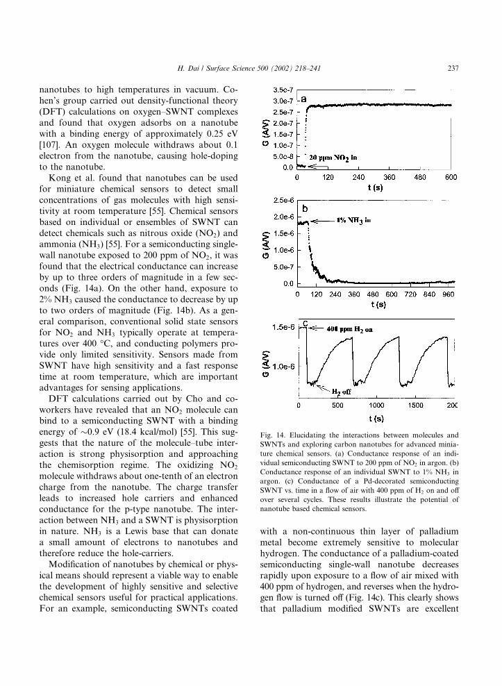
Kong et al. found that nanotubes can be usedfor miniature chemical sensors to detect smallconcentrations of gas molecules with high sensi-tivity at room temperature [55]. Chemical sensorsbased on individual or ensembles of SWNT candetect chemicals such as nitrous oxide (NO2) andammonia (NH3) [55]. For a semiconducting single-wall nanotube exposed to 200 ppm of NO2, it wasfound that the electrical conductance can increaseby up to three orders of magnitude in a few sec-onds (Fig. 14a). On the other hand, exposure to2% NH3 caused the conductance to decrease by upto two orders of magnitude (Fig. 14b). As a gen-eral comparison, conventional solid state sensorsfor NO2 and NH3 typically operate at tempera-tures over 400 �C, and conducting polymers pro-vide only limited sensitivity. Sensors made fromSWNT have high sensitivity and a fast responsetime at room temperature, which are importantadvantages for sensing applications.
DFT calculations carried out by Cho and co-workers have revealed that an NO2 molecule canbind to a semiconducting SWNT with a bindingenergy of �0.9 eV (18.4 kcal/mol) [55]. This sug-gests that the nature of the molecule–tube inter-action is strong physisorption and approachingthe chemisorption regime. The oxidizing NO2
molecule withdraws about one-tenth of an electroncharge from the nanotube. The charge transferleads to increased hole carriers and enhancedconductance for the p-type nanotube. The inter-action between NH3 and a SWNT is physisorptionin nature. NH3 is a Lewis base that can donatea small amount of electrons to nanotubes andtherefore reduce the hole-carriers.
Modification of nanotubes by chemical or phys-ical means should represent a viable way to enablethe development of highly sensitive and selectivechemical sensors useful for practical applications.For an example, semiconducting SWNTs coated
with a non-continuous thin layer of palladiummetal become extremely sensitive to molecularhydrogen. The conductance of a palladium-coatedsemiconducting single-wall nanotube decreasesrapidly upon exposure to a flow of air mixed with400 ppm of hydrogen, and reverses when the hydro-gen flow is turned off (Fig. 14c). This clearly showsthat palladium modified SWNTs are excellent
Fig. 14. Elucidating the interactions between molecules and
SWNTs and exploring carbon nanotubes for advanced minia-
ture chemical sensors. (a) Conductance response of an indi-
vidual semiconducting SWNT to 200 ppm of NO2 in argon. (b)
Conductance response of an individual SWNT to 1% NH3 in
argon. (c) Conductance of a Pd-decorated semiconducting
SWNT vs. time in a flow of air with 400 ppm of H2 on and off
over several cycles. These results illustrate the potential of
nanotube based chemical sensors.
H. Dai / Surface Science 500 (2002) 218–241 237
hydrogen sensors with fast response, good sensitiv-ity and reversibility under ambient conditions.The mechanism can be understood by consideringthe interactions between H2 and the Pd–SWNTsystem. It is well established that at room temper-ature, hydrogen molecules dissociate into atomichydrogen on Pd surfaces [108]. The resultingatomic hydrogen dissolves into Pd with high solu-bility and consequently lowers the work function(energy required to remove an electron from theFermi level) of Pd [108]. This causes electrontransfer from Pd to SWNTs, which lowers the hole-carriers in the nanotube and thus its conductance.
The Pd-modified SWNT sensors are readily re-versible when the hydrogen flow is stopped, as thedissolved atomic hydrogen in Pd combines withoxygen in air and leaves Pd–SWNT system in theform of water [108]. These features and mecha-nisms bear certain resemblance to conventionalhydrogen sensors based on semiconductor field-effect transistors with Pd gates, as pioneered byLundstrom [109].
6. Conclusion and outlook
Carbon nanotubes present significant opportu-nities to basic science and nanotechnology, andpose significant challenge for future work in thisfield. The approach of direct growth of nanowiresinto ordered structures on surfaces is a promisingroute to approach nanoscale problems and createnovel molecular-scale devices with advanced elec-trical, electromechanical and chemical functions.Gaining further control in nanotube growth willcontinue to open new possibilities in basic scienceand real-world applications. It is an ultimate goalfor growth to produce defect-free nanotubes at theton level by simple and efficient methods, gaincontrol over the nanotube chirality and diameter,and be able to direct the growth of a semicon-ducting or metallic nanowire from and to any de-sired sites.
Acknowledgements
We are grateful to Drs. C. Lieber, S. Iijima, P.McEuen, C. Dekker, Z. Yao, S. Xie and Z. Ren
for providing some of the data shown in thisarticle. Work carried out at Stanford were in col-laboration with Professors C. Quate, S. Fan, S. Y.Wu, C. S. Jayanthi, K. Cho, S. Manalis andC. Marcus, supported by National Science Foun-dation, DARPA/ONR, a Packard Fellowship,a Terman Fellowship, Semiconductor ResearchCorporation/Motorola Co., Semiconductor Re-search Corporation/Semetech, ABB Group Ltd.,the National Nanofabrication Users Network atStanford, Stanford Center for Materials Research,a Packard Fellowship for Science and Engineering,a Terman Fellowship, the Camile Henry-DreyfusFoundation and the American Chemical Society.
References
[1] H.W. Kroto, J.R. Heath, S.C. O’Brien, R.F. Curl, R.E.
Smalley, C60: Buckminsterfullerene, Nature 318 (1985)
162–163.
[2] S. Iijima, Helical microtubules of graphitic carbon,
Nature 354 (1991) 56–58.
[3] S. Iijima, T. Ichihashi, Single-shell carbon nanotubes of
1-nm diameter, Nature 363 (1993) 603–605.
[4] B.I. Yakobson, R.E. Smalley, Fullerene nanotubes:
C1;000;000 and beyond, Am. Sci. 85 (1997) 324–337.
[5] M.S. Dresselhaus, G. Dresselhaus, P.C. Eklund, Science
of Fullerenes and Carbon Nanotubes, Academic Press,
San Diego, 1996.
[6] N. Hamada, S. Sawada, A. Oshiyama, New one-dimen-
sional conductors: graphitic microtubules, Phys. Rev.
Lett. 68 (1992) 1579–1581.
[7] M.S. Dresselhaus, G. Dresselhaus, P. Avouris (Eds.),
Carbon Nanotubes, Springer, Berlin, 2001.
[8] T.W. Ebbesen, P.M. Ajayan, Large-scale synthesis of
carbon nanotubes, Nature 358 (1992) 220–222.
[9] D.S. Bethune, C.H. Kiang, M. DeVries, G. Gorman, R.
Savoy, J. Vazquez, R. Beyers, Cobalt-catalysed growth of
carbon nanotubes with single-atomic-layer walls, Nature
363 (1993) 605–607.
[10] A. Thess, R. Lee, P. Nikolaev, H. Dai, P. Petit, J. Robert,
C. Xu, Y. Lee, S. Kim, A. Rinzler, D. Colbert, G.
Scuseria, D. Tomanek, J. Fischer, R. Smalley, Crystalline
ropes of metallic carbon nanotubes, Science 273 (1996)
483–487.
[11] C. Journet, W. Maser, P. Bernier, A. Loiseau, M.
Delachapelle, S. Lefrant, P. Deniard, R. Lee, J. Fischer,
Large-scale production of single-walled carbon nanotubes
by the electric-arc technique, Nature 388 (1997) 756–758.
[12] G.G. Tibbetts, M.G. Devour, E.J. Rodda, An adsorption-
diffusion isotherm and its application to the growth of
carbon filaments on iron catalyst particles, Carbon 25
(1987) 367–375.
238 H. Dai / Surface Science 500 (2002) 218–241
[13] G.G. Tibbetts, Why are carbon filaments tubular? J.
Cryst. Growth 66 (1984) 632–638.
[14] R.T.K. Baker, Catalytic growth of carbon filaments,
Carbon 27 (1989) 315–323.
[15] H.G. Tennent, Hyperion Catalysis International, Inc. US
patent #4663230, USA, 1987.
[16] M. Endo, Grow carbon fibers in the vapor phase,
Chemtech 18 (1988) 568–576.
[17] H. Dai, Growth and characterization of carbon nano-
tubes, in: M.S. Dresselhaus, G. Dresselhaus, P. Avouris
(Eds.), Carbon Nanotubes, Springer, Berlin, 2001, pp.
29–53.
[18] J. Kong, A.M. Cassell, H. Dai, Chemical vapor deposi-
tion of methane for single-walled carbon nanotubes,
Chem. Phys. Lett. 292 (1998) 567–574.
[19] J. Kong, H. Soh, A. Cassell, C.F. Quate, H. Dai,
Synthesis of individual single-walled carbon nanotubes
on paterned silicon wafers, Nature 395 (1998) 878.
[20] A. Cassell, J. Raymakers, J. Kong, H. Dai, Large scale
single-walled nanotubes by CVD synthesis, J. Phys.
Chem. 103 (1999) 6484–6492.
[21] M. Su, B. Zheng, J. Liu, A scalable CVD method for the
synthesis of single-walled carbon nanotubes with high
catalyst productivity, Chem. Phys. Lett. 322 (2000) 321–
326.
[22] E. Flahaut, A. Govindaraj, A. Peigney, C. Laurent, C.N.
Rao, Synthesis of single-walled carbon nanotubes using
binary (Fe, Co, Ni) alloy nanoparticles prepared in situ by
the reduction of oxide solid solutions, Chem. Phys. Lett.
300 (1999) 236–242.
[23] J.-F. Colomer, C. Stephan, S. Lefrant, G. Tendeloo, I.
Willems, Z. K�oonya, A. Fonseca, C. Laurent, J. Nagy,
Large-scale synthesis of single-wall carbon nanotubes by
catalytic chemical vapor deposition (CCVD) method,
Chem. Phys. Lett. 317 (2000) 83–89.
[24] J. Hafner, M. Bronikowski, B. Azamian, P. Nikolaev, D.
Colbert, R. Smalley, Catalytic growth of single-wall
carbon nanotubes from metal particles, Chem. Phys. Lett.
296 (1998) 195–202.
[25] H. Cheng, F. Li, G. Su, H. Pan, M. Dresselhaus, Large-
scale and low-cost synthesis of single-walled carbon
nanotubes by the catalytic pyrolysis of hydrocarbons,
Appl. Phys. Lett. 72 (1998) 3282–3284.
[26] P. Nikolaev, M. Bronikowski, R. Bradley, F. Rohmund,
D. Colbert, K. Smith, R. Smalley, Gas-phase catalytic
growth of single-walled carbon nanotubes from carbon
monoxide, Chem. Phys. Lett. 313 (1999) 91–97.
[27] W.Z. Li, S. Xie, L. Qian, B. Chang, B. Zou, W. Zhou, R.
Zhao, G. Wang, Large-scale synthesis of aligned carbon
nanotubes, Science 274 (1996) 1701–1703.
[28] Z. Pan, S.S. Xie, B. Chang, C. Wang, Very long carbon
nanotubes, Nature 394 (1998) 631–632.
[29] Z.F. Ren, Z.P. Huang, J.W. Xu, J.H. Wang, Synthesis of
large arrays of well-aligned carbon nanotubes on glass,
Science 282 (1998) 1105–1107.
[30] S. Fan, M. Chapline, N. Franklin, T. Tombler, A. Cassell,
H. Dai, Self-oriented regular arrays of carbon nanotubes
and their field emission properties, Science 283 (1999)
512–514.
[31] H. Dai, J. Kong, C. Zhou, N. Franklin, T. Tombler, A.
Cassell, S. Fan, M. Chapline, Controlled chemical routes
to nanotube architectures, physics and devices, J. Phys.
Chem. 103 (1999) 11246–11255.
[32] H. Dai, Controlling nanotube growth, Phys. World 13
(2000) 43–47.
[33] A. Cassell, N. Franklin, T. Tombler, E. Chan, J. Han,
H. Dai, Directed growth of free-standing single-walled
carbon nanotubes, J. Am. Chem. Soc. 121 (1999) 7975–
7976.
[34] N. Franklin, H. Dai, An enhance chemical vapor depo-
sition method to extensive single-walled nanotube net-
works with directionality, Adv. Mater. 12 (2000) 890.
[35] H. Dai, J. Hafner, A. Rinzler, D. Colbert, R. Smalley,
Nanotubes for nanoprobes, Nature 384 (1996) 147–150.
[36] S. Wong, E. Joselevich, A. Woolley, C. Cheung, C.
Lieber, Covalently functionalized nanotubes as nanome-
trel-sized probes in chemistry and biology, Nature 394
(1998) 52–55.
[37] S. Wong, J. Harper, M. Lansbury, C.M. Lieber, Carbon
nanotube tips: high-resolution probes for imaging bio-
logical systems, J. Am. Chem. Soc. 120 (1998) 603–
604.
[38] H. Dai, N. Franklin, J. Han, Exploiting the properties of
carbon nanotubes for nanolithography, Appl. Phys. Lett.
73 (1998) 1508–1510.
[39] S. Wong, A. Wooley, E. Joselevich, C. Lieber, Func-
tionalization of carbon nanotube AFM probes using
tip-activated gases, Chem. Phys. Lett. 306 (1999) 219–
225.
[40] S. Wong, A. Woolley, E. Joselevich, C. Cheung, C.
Lieber, Covalently functionalized single-walled carbon
nanotube probe tips for chemical force microscopy,
J. Am. Chem. Soc. 120 (1998) 8557–8558.
[41] J. Hafner, C. Cheung, C. Lieber, Growth of nanotubes
for probe microscopy tips, Nature 398 (1999) 761–
762.
[42] J. Hafner, C. Cheung, C.M. Lieber, Direct growth of
single-walled carbon nanotube scanning probe micro-
scopy tips, J. Am. Chem. Soc. 121 (1999) 9750–9751.
[43] E.B. Cooper, S. Manalis, H. Fang, H. Dai, K. Matsu-
moto, S. Minne, T. Hunt, C.F. Quate, Terabit-per-square-
inch data storage with the atomic force microscope, Appl.
Phys. Lett. 29 (1999) 3566–3568.
[44] T. Odom, J. Huang, P. Kim, C.M. Lieber, Atomic
structure and electronic properties of single-walled carbon
nanotubes, Nature 391 (1998) 62–64.
[45] J.W.G. Wildoer, L.C. Venema, A.G. Rinzler, R.E. Smal-
ley, C. Dekker, Electronic structure of atomically resolved
carbon nanotubes, Nature 391 (1997) 59.
[46] M. Ouyang, J.-L. Huang, C.M. Lieber, Harvard Univer-
sity, unpublished results.
[47] T.W. Odom, J.L. Huang, P. Kim, C.M. Lieber, Structure
and electronic properties of carbon nanotubes, J. Phys.
Chem. 104 (2000) 2794–2809.
H. Dai / Surface Science 500 (2002) 218–241 239
[48] S.J. Tans, M. Devoret, H. Dai, A. Thess, R. Smalley,
L. Geerligs, C. Dekker, Individual single-wall carbon
nanotubes as quantum wires, Nature 386 (1997) 474–
477.
[49] M. Bockrath, D. Cobden, P. McEuen, N. Chopra, A.
Zettl, A. Thess, R. Smalley, Single-electron transport
in ropes of carbon nanotubes, Science 275 (1997) 1922–
1925.
[50] D. Cobden, M. Bockrath, N. Chopra, A. Zettle, P.
McEuen, A. Rinzler, R. Smalley, Spin splitting and even–
odd effects in carbon nanotubes, Phys. Rev. Lett. 81
(1998) 681–684.
[51] J. Nygard, D.H. Cobden, M. Bockrath, P.L. McEuen,
P.E. Lindelof, Electrical transport measurements on
single-walled carbon nanotubes, Appl. Phys. A 69 (1999)
297–304.
[52] H. Soh et al., Integrated nanotube circuits: controlled
growth and ohmic contacting of single-walled carbon
nanotubes, Appl. Phys. Lett. 75 (1999) 627–629.
[53] A. Morpurgo, J. Kong, C. Marcus, H. Dai, Gate
controlled superconducting proximity effect in nanotubes,
Science 286 (1999) 263–265.
[54] C. Zhou, J. Kong, H. Dai, Electrical measurements of
individual semiconducting single-walled nanotubes of
various diameters, Appl. Phys. Lett. 76 (1999) 1597.
[55] J. Kong, N. Franklin, C. Zhou, M. Chapline, S. Peng,
K. Cho, H. Dai, Nanotube molecular wires as chemical
sensors, Science 287 (2000) 622–625.
[56] C. Zhou, J. Kong, H. Dai, Intrinsic electrical properties of
single-walled carbon nanotubes with small band gaps,
Phys. Rev. Lett. 84 (2000) 5604.
[57] T. Tombler, C. Zhou, J. Kong, H. Dai, Gating individual
nanotubes and crosses with scanning probes, Appl. Phys.
Lett. 76 (2000) 2412.
[58] T. Tombler, C. Zhou, L. Alexeyev, J. Kong, H. Dai, L.
Liu, C. Jayanthi, M. Tang, S. Wu, Reversible nanotube
electro-mechanical characteristics under local probe ma-
nipulation, Nature 405 (2000) 769.
[59] Z. Yao, H.W.C. Postma, L. Balents, C. Dekker, Carbon
nanotube intramolecular junctions, Nature 402 (1999)
273–276.
[60] M.S. Fuhrer, J. Nyg�aard, L. Shih, M. Forero, Y. Yoon, M.
Mazzoni, H. Joon, J. Choi, S. Louie, A. Zettl, P. McEuen,
Crossed nanotube junctions, Science 288 (2000) 494–
497.
[61] T. Rueckes, K. Kim, E. Joselevich, G. Tseng, C. Cheung,
C. Lieber, Carbon nanotube-based nonvolatile random
access memory for molecular computing, Science 289
(2000) 94–97.
[62] C.T. White, T.N. Todorov, Carbon nanotubes as long
ballistic conductors, Nature 393 (1998) 240.
[63] H. Grabert, M.H. Devoret (Eds.), Single Charge Tunnel-
ing, Plenum Press, New York, 1992.
[64] J.E. Fischer, H. Dai, A. Thess, R. Lee, N. Hanjani, D. De
Haas, R. Smalley, Metallic resistivity in crystalline ropes
of single-wall carbon nanotubes, Phy. Rev. B-Condens.
Matter 55 (1997) R4921–R4924.
[65] C.L. Kane, E. Mele, R. Lee, J. Fischer, P. Petit, H. Dai,
A. Thess, R. Smalley, A. Verschueren, A. Tans, C.
Dekker, Temperature dependent resistivity of single wall
carbon nanotubes, Euro. Phys. Lett. 6 (1998) 683–688.
[66] H.R. Shea, R. Martel, M. Avouris, Electrical transport in
rings of single-wall nanotubes: one-dimensional localiza-
tion, Phys. Rev. Lett. 84 (2000) 4441.
[67] Z. Yao, C. Dekker, personal communication.
[68] A. Bachtold, M. Fuhrer, S. Plyasunov, M. Forero, E.
Anderson, A. Zettl, P. McEuen, Scanned probe micro-
scopy of electronic transport in carbon nanotubes, Phys.
Rev. Lett. 84 (2000) 6082–6085.
[69] S. Tans, A. Verschueren, C. Dekker, Room-temperature
transistor based on a single carbon nanotube, Nature 393
(1998) 49–52.
[70] R. Martel, T. Schmidt, H.R. Shea, T. Hertel, P. Avouris,
Single- and multi-wall carbon nanotube field-effect tran-
sistors, Appl. Phys. Lett. 73 (1998) 2447–2449.
[71] P.G. Collins, K. Bradley, M. Ishigami, A. Zettl, Extreme
oxygen sensitivity of electronic properties of carbon
nanotubes, Science 287 (2000) 1801–1804.
[72] L. Chico, V.H. Crespi, L.X. Benedict, S.G. Louie, M.L.
Cohen, Pure carbon nanoscale devices—nanotube hetero-
junctions, Phys. Rev. Lett. 76 (1996) 971–974.
[73] R.S. Lee, H.J. Kim, J.E. Fischer, A. Thess, R.E. Smalley,
Conductivity enhancement in single-wall carbon nano-
tube bundles doped with K and Br, Nature 388 (1997)
255–257.
[74] L. Grigorian, K. Williams, S. Fang, G. Sumanasekera, A.
Loper, E. Dickey, S. Pennycook, P. Eklund, Reversible
intercalation of charged iodine chains into carbon nano-
tube ropes, Phys. Rev. Lett. 80 (1998) 5560–5563.
[75] R.S. Lee, H. Kim, J. Fischer, J. Lefebvre, M. Radosavlj-
evi, J. Hone, A. Johnson, Transport properties of a
potassium-doped single-wall carbon nanotube rope, Phys.
Rev. B 61 (2000) 4526–4529.
[76] M. Bockrath, J. Hone, A. Zettl, P. McEuen, A. Rinzler,
R. Smalley, Chemical doping of individual semiconduct-
ing carbon-nanotube ropes, Phys. Rev. B 61 (2000)
R10606–R10608.
[77] J. Kong, C. Zhou, E. Yenilmez, H. Dai, Alkaline metal
doped n-type semiconducting nanotubes as quantum dots,
Appl. Phys. Lett. 77 (2000) 3977.
[78] H. Ishikuro, T. Fujii, T. Saraya, G. Hashiguchi, T.
Hiramoto, T. Ikoma, Coulomb blockade oscillations at
room temperature in a Si quantum wire metal-oxide-
semiconductor field-effect transistor fabricated by aniso-
tropic etching on a silicon-on-insulator substrate, Appl.
Phys. Lett. 68 (1996) 3585–3587.
[79] H. Ishikuro, T. Hiramoto, Quantum mechanical effects in
silicon quantum dot in a single-electron transistor, Appl.
Phys. Lett. 71 (1997) 3691–3693.
[80] L. Zhuang, L. Guo, S.Y. Chou, Silicon single-electron
quantum-dot transistor switch operating at room temper-
ature, Appl. Phys. Lett. 72 (1998) 1205–1207.
[81] K. Matsumoto, M. Ishii, K. Segawa, Y. Oka, B. Varta-
nian, J. Harris, Room temperature operation of a single
240 H. Dai / Surface Science 500 (2002) 218–241
electron transistor made by the scanning tunneling
microscope nanooxidation process for the TiOx/Ti system,
Appl. Phys. Lett. 68 (1996) 34–36.
[82] Y.A. Pashkin, Y. Nakamura, J.S. Tsai, Room-tempera-
ture Al single-electron transistor made by electron-beam
lithography, Appl. Phys. Lett. 76 (2000) 2256–2258.
[83] M. Nardelli, J. Bernholc, Mechanical deformations and
coherent transport in carbon nanotubes, Phys. Rev. B 60
(1998) R16338–16341.
[84] A. Rochefort, D. Salahub, P. Avouris, The effect of
structural distortions on the electronic structure of carbon
nanotubes, Chem. Phys. Lett. 297 (1998) 45–50.
[85] A. Rochefort, F. Lesage, D. Salhub, P. Avouris, Con-
ductance of distorted carbon nanotubes, 1999 xxx.lanl.
gov/cond-mat/9904083.
[86] L. Liu, C. Jayanthi, M. Tang, S.Wu, T. Tombler, C. Zhou,
L. Alexeyev, J. Kong, H. Dai, Controllable reversibility of
an transition of a sp2 to sp3 single wall nanotube under the
manipulation of an AFM tip: a nanoscale electromechan-
ical switch? Phys. Rev. Lett. 84 (2000) 4950.
[87] H. Dai, E.W. Wong, Y.Z. Lu, F. Shoushan, C.M. Lieber,
Synthesis and characterization of carbide nanorods,
Nature 375 (1995) 769–772.
[88] W.Q. Han, S.S. Fan, Q.Q. Li, Y.D. Hu, Synthesis of
gallium nitride nanorods through a carbon nanotube-
confined reaction, Science 277 (1997) 1287–1289.
[89] A. Bezryadin, C.N. Lau, M. Tinkham, Quantum sup-
pression of superconductivity in ultrathin nanowires,
Nature 404 (2000) 971.
[90] Q. Ma, A. Rosenberg, Interaction of Ti with the (0001)
surface of highly oriented pyrolytic graphite, Phys. Rev. B
60 (1999) 2827–2832.
[91] M. Baumer, J. Libuda, H. Freund, The temperature
dependent growth mode of nickel on the basal plane of
graphite, Surf. Sci. 327 (1995) 321–329.
[92] P. Kruger, A. Rakotomahevitra, J. Parlebas, C. Deman-
geat, Magnetism of epitaxial 3d-transition-metal mono-
layer on graphite, Phys. Rev. B (1998) 5276–5280.
[93] S.S. Peng, B.R. Cooper, Y.G. Hao, Modeling of adsorp-
tion of iron impurities at the surface of graphite, Philo.
Mag. 73 (1996) 611–617.
[94] D. Tomanek, W. Zhong, Palladium–graphite interaction
potentials based on first-principles calculations, Phys.
Rev. B 43 (1991) 12623–12625.
[95] Q. Ma, R. Rosenberg, Interaction of Al clusters with the
(0001) surface of highly oriented pyrolytic graphite, Surf.
Sci. 391 (1997) L1224–1229.
[96] I. Moulett, Ab-initio molecular-dynamics study of the
interaction of aluminum clusters on a graphite surface,
Surf. Sci. 333 (1995) 697–702.
[97] E. Ganz, K. Sattler, J. Clarke, Scanning tunneling
microscopy of Cu, Ag, Au and Al adatoms small clusters,
and islands on graphite, Surf. Sci. 219 (1989) 33–67.
[98] L. Barfotti, P. Jensen, A. Hoareau, M. Treilleux, B.
Cabaud, A. Perez, F. Aires, Diffusion and aggregation of
large antimony and gold clusters deposited on graphite,
Surf. Sci. 367 (1996) 276.
[99] J. Arthur, A. Cho, Adsorption and desorption kinetics of
Cu and Au on (0001) graphite, Surf. Sci. 36 (1973) 641–
660.
[100] T.R. Ohno, Y. Chen, S. Harvey, G. Kroll, J. Weaver, R.
Haufler, R. Smalley, C60 bonding and energy-level align-
ment on metal and semiconductor surfaces, Phys. Rev. B
44 (1991) 13747–13755.
[101] V. Vijayakrishnan, A. Santra, R. Seshadri, R. Nagarajan,
T. Pradeep, C. Rao, A comparative study of the interac-
tion of nickel clusters with buckministerfullerene C60 and
graphite, Surf. Sci. 262 (1992) L87–90.
[102] E. Parks, K. Kerns, S.R.B. Winter, Adsorption of C60 on
nickel clusters at high temperatures, Phys. Rev. B 59
(1999) 13431.
[103] M. Menon, A. Andriotis, G. Froudakis, Curvature
dependence of metal catalyst atom interaction with
carbon nanotubes walls, Chem. Phys. Lett. 320 (2000)
425–434.
[104] Y. Zhang, N. Franklin, R. Chen, H. Dai, A metal coating
study of suspended carbon nanotubes and its implications
to metal-tube interactions, Chem. Phys. Lett. 331 (2000)
35–41.
[105] T. Tachibana, B. Williams, J. Glass, Correlation of the
electrical properties of metal contacts on diamond films
with the chemical nature of the metal–diamond surface.
II. Titanium contacts: a carbide forming metal, Phys. Rev.
B 45 (1992) 11975–11981.
[106] J. Kong, H. Dai, unpublished results.
[107] S. Jhi, S.G. Louie, M.L. Cohen, Electronic properties of
oxidized carbon nanotubes, Phys. Rev. Lett. 85 (2000)
1710.
[108] A. Mandelis, C. Christofides, Physics Chemistry and
Technology of Solid State Gas Sensor Devices, Wiley,
New York, 1993.
[109] I. Lundstrom, M. Shivaraman, C. Svensson, Chemical
reactions on palladium surfaces studied with Pd-MOS
structures, Surf. Sci. 64 (1977) 497.
H. Dai / Surface Science 500 (2002) 218–241 241