Center ANCE NU - Northwestern...
28
NUANCE Center Northwestern University Atomic and Nanoscale Experimental Characterization Center Professor Vinayak P. Dravid, Ph.D. Director
Transcript of Center ANCE NU - Northwestern...

NUANCE CenterNorthwestern University
Atomic and Nanoscale Experimental Characterization Center
Professor Vinayak P. Dravid, Ph.D.
Director
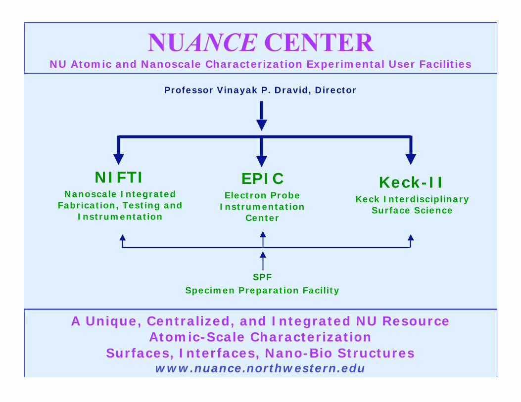
NUANCE CENTERNU Atomic and Nanoscale Characterization Experimental User Facilities
NIFTINanoscale Integrated
Fabrication, Testing and
Instrumentation
Keck-IIKeck Interdisciplinary
Surface Science
EPICElectron Probe
Instrumentation
Center
A Unique, Centralized, and Integrated NU Resource
Atomic-Scale Characterization
Surfaces, Interfaces, Nano-Bio Structureswww.nuance.northwestern.edu
Professor Vinayak P. Dravid, Director
SPF
Specimen Preparation Facility

Contact Angle
Zeta Potential and Particles SizeControlled Vacuum Evaporation
Controlled Atmosphere Ovens
Plasma Cleaning System
Cryo-Preparation Laminar Flow Hoods with Sonicators
Controlled Atmosphere Spin Coaters
Dip-Pen Nanolithography (DPN)
Microcontact Printing (mCP)
Nanoimprint Lithography (NIL)
FEG Electron Beam Lithography (eBL)
Focused Ion Beam (FIB)
ToF-SIMS, XPS, UHV STM/AFM
4 SEMs, 3 TEMsEnergy Filtered Cryo-TEM
SNOM, with Femto-s Spectroscopy
Surface Plasmon Resonance (SPR)
Scanning Molecular Force ProbeLaser Fluorescence Optical Microscope
FTIR Microscopy/Spectroscopy
Soft and Hard Lithography
Nano- to Microscale
Measurement/Testing
& Preparation
Imaging, Spectroscopy and Analysis
Nano- to Microscale
Keck-I Biophysics APS-CATs
NUANCE CENTER
Facility Collaboration

NUANCE CENTER
Integrated Atomic-Nanoscale Surface/InterfaceBio/Nano Analytical Capabilities
Merging Length-ScalesFrom Micro-to Nanoscale Fabrication and Analysis
Complete and Open-AccessTrainingCollaborationUser Feed-back
Complementary CapabilitiesKeck BiophysicsArgonne-CATs

EPIC & Sample Prep

Managers for EPIC
TEM: Jian-Guo Zheng, Ph.D. & Shuyou Li, Ph.D.
SEM: Ben Myers
Gajendra Shekhawat, Ph.D. also on Quanta
Specimen Preparation: Shuyou Li, Ph.D.

Electron Probe Instrumentation Center
• Transmission Electron Microscopes — TEM(JEOL JEM-2100F, Hitachi HF-2000, H-8100)
• Scanning Electron Microscopes — SEM(LEO Gemini 1525, Hitachi S-4500, S-3500,FEI Quanta 600)
• Focused Ion Beam — FIB(Hitachi FIB 2000A)
TEM SEM
FIB

Electron diffraction patterns of a membrane
protein: Before and after energy filtering
Atomic resolution of HfO2/SiO2/Si
Atomic resolution of novel
carbon nanostructure
Elemental mapping of Fe-B nano-capsules

DNA-linked gold nanoparticles
Focused Ion Beam:
Site- and shape-specific
trenches for microfluidicsLiposome-nanoparticle
assembly for drug/gene delivery
CdSe nano-material:
Bright/dark field micrographs and diffraction pattern
Gold flowers
Nano-diffraction pattern from nano-Ag
prisms

Nano-cheerios!
Hollow nanoparticles of Pd catalyst
Poly-crystal grains via EBSD—
Mapping crystallography and orientation
Orientational imaging

Image of Ebola virus depicting
the deadly thread morphology
Processed cheese:
Note the fat globules!
Images of human dentinal
Alumina FE tipNano-fetti

Sample Preparation Facility
• Complete Metallography Set-Up
• JEOL Carbon Evaporator
• Fischione Plasma Cleaner
• For TEM—
– VCR Precision Dimplers
– Gatan Dry Pumping Station
– South Bay Electropolisher (Single Jet)
• Ultrasonic and Slurry Disc Cutters
• Precision Ion Polishing System
• IBT

Keck-II

Manager for Keck-II
Nick Wu, Ph.D.

Keck Interdisciplinary Surface Science
• Fourier Transform Infrared Spectroscopy (FT-IR)
• Time-of-Flight Ion Mass Spectrometry (ToF-SIMS)
• Ultra-high Vacuum Scanning Tunneling
Microscopy/Atomic Force Microscopy
(UHV STM/AFM)
• X-ray Photoelectron Spectroscopy (XPS/ESCA)

Focus: surface analysis and nano-scale characterization
Commission: research, collaboration, education and outreach
SIMS-PHI TRIFT IIUHV STM/AFM-Omicron
XPS-OmicronDigital Instrument SPM
Keck-II Power

Chemical map of Mg/MgB2 composite using SIMS
Boron map Mg map

STM image, atomic terrace of Au
STM image, HOPG

NIFTI

NIFTI Manager
Gajendra Shekhawat, Ph.D.
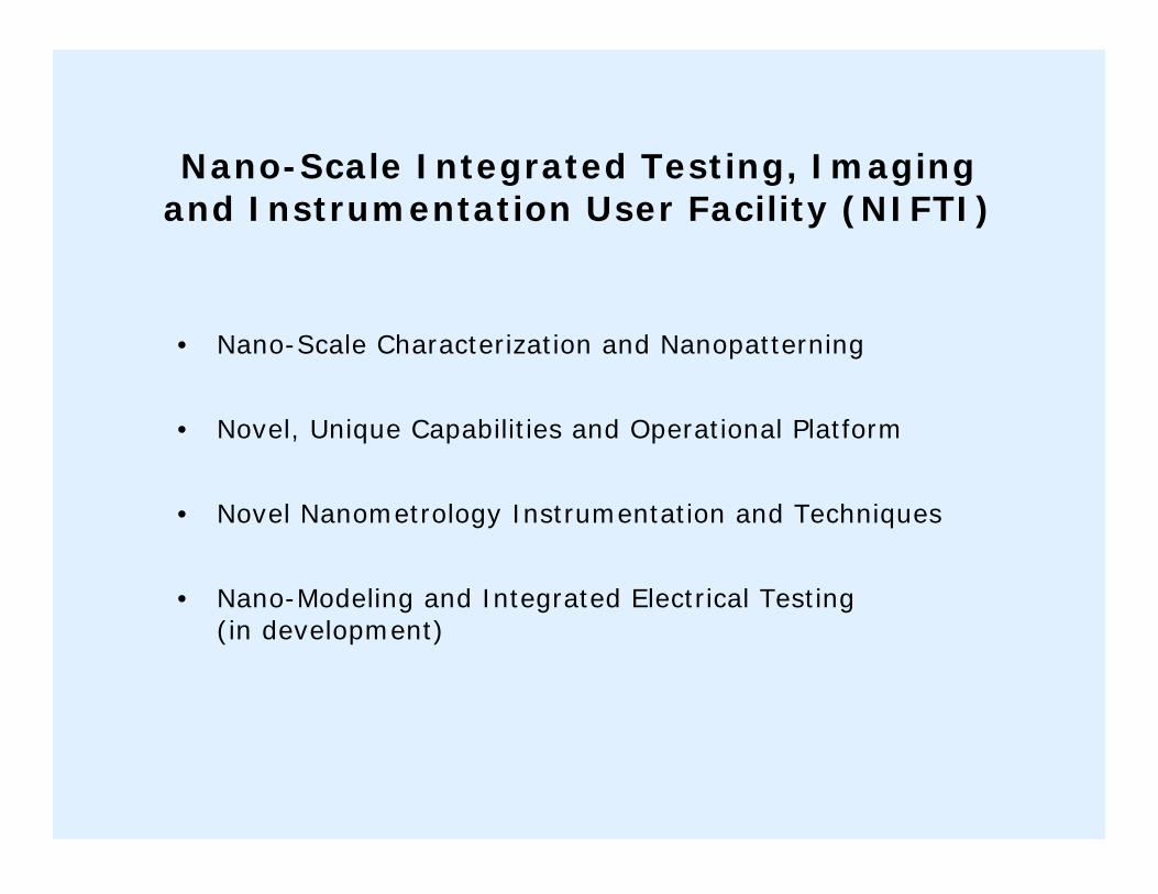
Nano-Scale Integrated Testing, Imagingand Instrumentation User Facility (NIFTI)
• Nano-Scale Characterization and Nanopatterning
• Novel, Unique Capabilities and Operational Platform
• Novel Nanometrology Instrumentation and Techniques
• Nano-Modeling and Integrated Electrical Testing(in development)

Nano-modelling and Integrated
Electrical Testing
Nano-Scale
Characterization
& Nanopatterning
Novel and Unique Capabilities
& Operational Platform
Sample
tip piezo
Stress (MPa)
+14.1
-10.1
Novel Nanometrology
Instrumentation & Techniques
NIFTI
Broad Outreach

Nanofabrication &
Surface Probe
Characterization
Instrumentation
NanoInk NSCRIPTOR
JEOL Environmental SPM Pico Force Microscope
Femto-NSOM Digital Instrument SPM
The NIFTI Arsenal
2.5 m 5 m
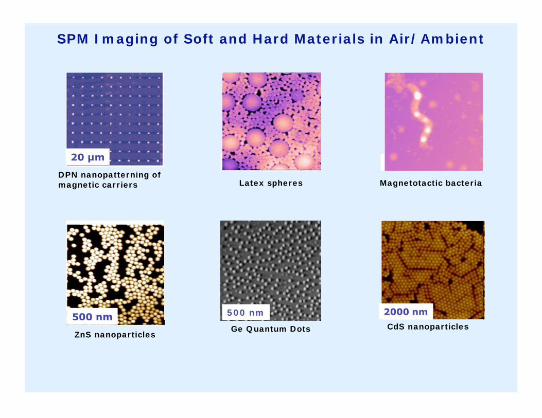
ZnS nanoparticles
500 nm500 nm
SPM Imaging of Soft and Hard Materials in Air/Ambient
Latex spheres Magnetotactic bacteriaDPN nanopatterning of
magnetic carriers
20 m
Ge Quantum Dots
500 nm500 nm
CdS nanoparticles
2000 nm2000 nm

JEOL and NSOM Imaging of Soft and Hard Materials
in Air/Vacuum
25 m
Transmission NSOM image of
check board patterns on glass
12 m
Nano-hole arrays with NSOM
Single wall carbon nanotubeDNA
Pores in AO membrane Self-assembled organic molecules

PROJECTED PERFORMANCE GAINS
Nanostructural Metrology
In-Line 3D Nanomechanical Imaging
nondestructive surface/ subsurface defect
identification
XY resolution: < 1nm
Z resolution < 2 nm (defect size)
Sub-surface high resolution “modulus”
imaging
In-vitro imaging of biopolymer,
biomaterials and biological structures
Development of a Unique Near-Field Ultrasonic
Holography (NFAH) System on JEOL 5200 Platform
sample piezosample piezo
wSSam
ple
Sam
ple
tip piezo
AFM tipAFM tip
wTip
Acoustic object waves excited through waferAcoustic object waves excited through wafer
Eliminate Far-Field Acoustic Lenses
and Couplers
Detect phase of transmitted acoustic
wave directly at wafer/device surface:
Eliminate coupling fluid

NFAHAFM
1.5 1.5 mm800 nm800 nm
Defects in Spin on Dielectric TrenchesDefects in Cu Trenches at 50 nm below from Surface
AFM NFAH
Looking Inside Carbon Nanotubes
“Proof-of-Concept”

Administrative Staff for NUANCE Center
Ruth McCullough, Business Manager
Carolyn Turek, Program Assistant
NUANCE email: [email protected]
Web site: www.nuance.northwestern.edu