
Balanced Routing of Dual-Rail Signals for DPA-Resistant ... · RSL Random Switching Logic SABL...
91
Master’s Thesis Balanced Routing of Dual-Rail Signals for DPA-Resistant Logic Styles in Xilinx FPGAs Vincent Immler September 3, 2013 Faculty of Electrical Engineering and Information Technology Horst Görtz Institute for IT-Security Prof. Dr.-Ing. Christof Paar Advisor: Dr. Amir Moradi
Transcript of Balanced Routing of Dual-Rail Signals for DPA-Resistant ... · RSL Random Switching Logic SABL...

Master’s Thesis
Balanced Routing of Dual-Rail Signals for
DPA-Resistant Logic Styles in Xilinx
FPGAs
Vincent Immler
September 3, 2013
Faculty of Electrical Engineering and Information Technology
Horst Görtz Institute for IT-Security
Prof. Dr.-Ing. Christof Paar
Advisor: Dr. Amir Moradi

Author’s contact information:
57dcb65dac6c9f6e1a6bd27ae8953e79f9922120
2013-10-10 22:26:42 +0200
Copyright © 2013 by Vincent Immler.
All rights reserved.

To my wife and family

Abstract
Side-channel attacks are a powerful technique against cryptographic implementations.
Hence, it is necessary to design efficient and effective countermeasures.
Mainly two approaches have been suggested to reduce side-channel leakage, namely
masking and hiding. The former modifies the cryptographic algorithm by blinding val-
ues with random masks before their computation. This requires a true random number
generator and also depends on the order of the masking. The latter is usually realized by
implementing a kind of dual-rail logic style that aims at equalizing the power consumption
level, thereby minimizing possible leakages. This approach almost always results in circuits
that need to be developed and securely manufactured separately from the rest of the circuit
to prevent adversarial leakages. Other effects such as the early-propagation effect addi-
tionally increase the level of difficulty to implement such schemes, in particular in Field
Programmable Gate Arrays (FPGAs). Unlike specific ASIC tools, no FPGA development
tools are known that would allow to place and route sensitive logic in a way that would
minimize the occurring leakage.
To address these issues, we implement a new asynchronous secure logic style based on
WDDL that is especially designed for FPGA platforms. While this logic style has proven
to be more robust by default, we further increase the level of security by developing a
customized router that is used to control the routing of the sensitive logic in such a way
that the leakage is diminished.
In our experiments, we observe a significantly increased resistance against side-channel
attacks compared to a default routing created by ISE for the same logic style.
Our result shows that by implementing a secure logic style in FPGAs a very high level of
security can be achieved. Furthermore, we exhibit how enhancing the development flow
can lead to reduced leakages for FPGAs.
Keywords Cryptography, Embedded, Security, FPGA, Asynchronous, Secure Logic Style,
XDL, Side Channel Analysis, Countermeasure, RapidSmith, SAT, Routing


Declaration
I hereby declare that this submission is my own work and that, to the best of my knowledge
and belief, it contains no material previously published or written by another person
nor material which to a substantial extent has been accepted for the award of any other
degree or diploma of the university or other institute of higher learning, except where due
acknowledgment has been made in the text.
Erklärung
Hiermit versichere ich, dass ich die vorliegende Arbeit selbstständig verfasst und keine
anderen als die angegebenen Quellen und Hilfsmittel benutzt habe, dass alle Stellen der
Arbeit, die wörtlich oder sinngemäß aus anderen Quellen übernommen wurden, als solche
kenntlich gemacht sind und dass die Arbeit in gleicher oder ähnlicher Form noch keiner
Prüfungsbehörde vorgelegt wurde.
Ort, Datum Vincent Immler


Acknowledgements
First of all, I would like to express my gratitude to my advisor Amir Moradi, who offered
me to work on this incredibly interesting topic. I truly appreciate his guidance and support
on every aspect throughout my thesis. Without his encouragement and assistance, this
thesis would not have been possible.
Furthermore, I would like to thank Ali Ahari for working out the LUT based LEDR im-
plementation during his visit at the Embedded Security Group which significantly lowered
the effort to implement AWDDL. Special thanks also go to my former boss Christopher
Wolf for getting me started in using a SAT solver.
Of course, a huge “thank you” to the people from the Brigham Young University for
publishing RapidSmith as an open source project. Clearly, without their previous work my
thesis would have been a lot more difficult to realize.
Finally, I would also like to thank my fellow students Dennis, Benno, Marcus, Andy, and
Alex for their true friendship, especially in the latter days of my studies.


By three methods we may learn wisdom:first, by reflection, which is noblest;second, by imitation, which is easiest;and third, by experience, which is the most bitter.
CONFUCIUS

Contents
Nomenclature xv
1 Introduction 1
1.1 Motivation . . . . . . . . . . . . . . . . . . . . . . . . . . . . . . . . . . . . 1
1.2 Related Work . . . . . . . . . . . . . . . . . . . . . . . . . . . . . . . . . . . 2
1.3 Contribution . . . . . . . . . . . . . . . . . . . . . . . . . . . . . . . . . . . 2
1.4 Outline . . . . . . . . . . . . . . . . . . . . . . . . . . . . . . . . . . . . . . 3
2 Mathematical Background 5
2.1 SAT solving . . . . . . . . . . . . . . . . . . . . . . . . . . . . . . . . . . . 5
2.1.1 Basic Terminology . . . . . . . . . . . . . . . . . . . . . . . . . . . 5
2.1.2 Encoding for Selecting Objects . . . . . . . . . . . . . . . . . . . . 5
2.1.3 Encoding for Selecting Sets of Objects . . . . . . . . . . . . . . . . 6
2.1.4 Encoding of Selection Conflicts . . . . . . . . . . . . . . . . . . . . 7
2.1.5 SAT Solvers: Dimacs File Format . . . . . . . . . . . . . . . . . . . 8
2.2 Practical Example using SAT: Exact Cover Problem . . . . . . . . . . . . . 8
2.3 Information and Probability Theory . . . . . . . . . . . . . . . . . . . . . . 10
2.3.1 Probability Space . . . . . . . . . . . . . . . . . . . . . . . . . . . . 11
2.3.2 Discrete Random Variable and Expected Value . . . . . . . . . . . . 11
2.3.3 Variance and Standard Deviation . . . . . . . . . . . . . . . . . . . 11
2.3.4 Covariance and Correlation Coefficient . . . . . . . . . . . . . . . . 12
2.3.5 Entropy and Mutual Information . . . . . . . . . . . . . . . . . . . 12
3 Technical Background 15
3.1 FPGAs . . . . . . . . . . . . . . . . . . . . . . . . . . . . . . . . . . . . . . 15
3.1.1 Architecture of FPGAs . . . . . . . . . . . . . . . . . . . . . . . . . 15
3.1.2 Other Functional Blocks . . . . . . . . . . . . . . . . . . . . . . . . 18
3.1.3 Design Flow . . . . . . . . . . . . . . . . . . . . . . . . . . . . . . . 18
3.1.4 Routing Algorithms and Metrics . . . . . . . . . . . . . . . . . . . 19
3.2 Xilinx Virtex 5 Routing Architecture . . . . . . . . . . . . . . . . . . . . . . 20
3.2.1 Overview . . . . . . . . . . . . . . . . . . . . . . . . . . . . . . . . 20
3.2.2 Wire Naming Convention . . . . . . . . . . . . . . . . . . . . . . . 21
3.2.3 Xilinx Routing and Directed Routing Constraints (DIRTs) . . . . . 24
3.3 XDL – Xilinx Design Language . . . . . . . . . . . . . . . . . . . . . . . . . 26
3.3.1 XDL Files . . . . . . . . . . . . . . . . . . . . . . . . . . . . . . . . 26
3.3.2 XDLRC Files . . . . . . . . . . . . . . . . . . . . . . . . . . . . . . . 30
3.3.3 File Format Conversion and Limitations . . . . . . . . . . . . . . . 30
3.4 Secure Logic Styles . . . . . . . . . . . . . . . . . . . . . . . . . . . . . . . 30
3.4.1 Idea and Concepts of Side-Channel Analysis . . . . . . . . . . . . . 31
3.4.2 WDDL – Synchronous Secure Logic Style . . . . . . . . . . . . . . 32
xiii
Contents
3.4.3 Asynchronous Logic Styles . . . . . . . . . . . . . . . . . . . . . . 33
4 Implementation 37
4.1 RapidSmith Library . . . . . . . . . . . . . . . . . . . . . . . . . . . . . . . 37
4.1.1 Introduction to RapidSmith . . . . . . . . . . . . . . . . . . . . . . 37
4.1.2 Routing using RapidSmith . . . . . . . . . . . . . . . . . . . . . . . 39
4.2 Customized Router using RapidSmith . . . . . . . . . . . . . . . . . . . . . 39
4.2.1 Customized Workflow Overview . . . . . . . . . . . . . . . . . . . 40
4.2.2 Router Structure . . . . . . . . . . . . . . . . . . . . . . . . . . . . 43
4.2.3 Implementation Considerations . . . . . . . . . . . . . . . . . . . . 46
4.3 FPGA Approach to Secure Logic . . . . . . . . . . . . . . . . . . . . . . . . 48
4.4 Determining FPGA Settings . . . . . . . . . . . . . . . . . . . . . . . . . . 50
5 Measurement Environment 53
5.1 SASEBO-GII Side-Channel Attack Platform . . . . . . . . . . . . . . . . . . 53
5.2 Oscilloscope / Settings . . . . . . . . . . . . . . . . . . . . . . . . . . . . . 54
6 Practical Results 55
6.1 Obtained Routings . . . . . . . . . . . . . . . . . . . . . . . . . . . . . . . . 55
6.2 Practical Investigations . . . . . . . . . . . . . . . . . . . . . . . . . . . . . 56
6.3 Implications . . . . . . . . . . . . . . . . . . . . . . . . . . . . . . . . . . . 58
7 Conclusion 59
7.1 Summary . . . . . . . . . . . . . . . . . . . . . . . . . . . . . . . . . . . . . 59
7.2 Future Work . . . . . . . . . . . . . . . . . . . . . . . . . . . . . . . . . . . 59
A Xilinx Virtex 5 Routing Architecture 61
A.1 Interconnect Illustrations . . . . . . . . . . . . . . . . . . . . . . . . . . . . 61
B Source Code and Used Software Versions 63
List of Figures 65
List of Tables 67
Algorithms 68
Listings 71
Bibliography 73
xiv

Nomenclature
Abbreviations
AES Advanced Encryption Standard
AMO At-Most-One encoding
ANF Algebraic Normal Form
API Application Programming Interface
ASCII American Standard Code for Information Interchange
ASIC Application Specific Integrated Circuit
BRAM Block Random Access Memory
CLB Configurable Logic Block
CMOS Complementary Metal Oxide Semiconductor
CNF Conjunctive Normal Form
CPA Correlation Power Analysis
CSP Constraint Satisfaction Problem
DCM Digital Clock Manager
DEMA Differential Electro-Magnetic Analysis
DIRT Directed Routing Constraint
DPA Differential Power Analysis
DPL Dual-Rail Precharge Logic
DSP Digital Signal Processor
DUT Device Under Test
DWDDL Double Wave Dynamic Differential Logic (WDDL)
EDA Electronic Design Automation
EMA Electromagnetic Analysis
FF Flip-Flop
FPGA Field Programmable Gate Array
GND Ground
HDL Hardware Description Language
IOB Input/Output Buffer
ISE Integrated Software Environment
LEDR Level-Encoded Dual-Rail Logic
LUT Look-Up Table
NCD Native Circuit Description
PAR Place & Route
PCB Printed Circuit Board
PIP Programmable Interconnect Point
PROM Platform Read-Only Memory
RAM Random Access Memory
ROM Read-Only Memory
RPM Relatively Placed Macro. Same as Relationally Placed Macro
xv

Nomenclature
RSL Random Switching Logic
SABL Sense-Amplifier Based Logic
SAT (Boolean) Satisfiability
SCA Side Channel Analysis
SPA Simple Power Analysis
SRAM Static Random Access Memory
TRNG True Random Number Generator
UCF User Constraint File
VHDL VHSIC (Very High Speed Integrated Circuit) Hardware Description
Language
WDDL Wave Dynamic Differential Logic
XDL Xilinx Description Language
XOR Exclusive OR
Symbols
(·,·) Indicates a dual-rail signal
< · > Indicates signal n of a net
Superscripts
C Denotes a complementary net
xvi
1 Introduction
Since cryptography has heavily evolved and most implemented schemes have a sound
foundation ofwell-analyzedmath, it has become unlikely to have complete security breaches
by analytical means. Most attacks therefore concentrate on Side Channel Analysis (SCA)
or the exploitation of the software running on the device. While software or protocol
exploitation tends to have a different target (e. g., code injection, privilege escalation, . . . )
compared to SCA, it is the latter which usually aims at revealing the secret key of a
cryptographic scheme.
In the recent past, many practical examples have demonstrated the significance of these
side-channel attacks, especially power analysis, for instance, KeeLoq and Mifare Classic
[Eis+08; KOP09] were both broken by such attacks (and flawed designs). Hence, it is an
ongoing effort to enhance countermeasures (and attacks) to improve side-channel resistance.
1.1 Motivation
To thwart side-channel analysis, various countermeasures have been proposed in the past.
Some of these countermeasures can be defeated just by a higher number of measured
traces or preprocessing techniques, such as added noise or random delays. Others, such as
masking, require a tamper-resistant True Random Number Generator (TRNG) whereas the
order of the masking scheme is also of importance.
As another approach to mitigate side-channel leakage, customized logic styles have
been developed to reduce (or prevent) the information leakage. However, the majority of
proposed secure circuit techniques concentrate on Application Specific Integrated Circuits
(ASICs). While this allows full control over the design flow, it results in circuits that
need to be developed and securely manufactured separately, thus causing additional cost
and basically having all the disadvantages of an ASIC. For example, while FPGAs can
be configured and updated in the field, ASICs are fixed and cannot be updated without
additional cost. Due to their nature, FPGAs already feature a platform that is highly regular
in its hardware structure which makes it an interesting target to implement secure logic
styles in them, possibly saving the cost for a separate cryptographic unit. Considering
partial dynamic reconfiguration, this could potentially lead to situations where no area is
occupied by the cryptographic engine (at times when it is not used) or to a heavily reduced
area consumption if multiple engines for different schemes are used.
Unfortunately, there is only very few research in this area and commercially available
design tools do not allow to control placement and routing in a way that would be beneficial
for side-channel resistance. Implementing such schemes and verifying their security is
therefore still an unfulfilled requirement. While it is unlikely to outperform implementations
in ASICs in terms of security, it may be possible to offer reasonable security margins without
the extra cost of an ASIC. This could also lead to shorter development cycles.
One of the research directions in secure logic styles favors asynchronous circuits because
of the lack of a timing reference. At least one attempt was made to verify the effectiveness
1

1 Introduction
of this approach [Tam12], which turned out not to be successful. This is presumably owed
to the fact that the underlying problem of imbalanced routing paths was not targeted.
The goal of this thesis is therefore not only to implement secure logic styles but to
implement them in a secure manner taking the routing imbalances into consideration.
This is done by replacing steps of the original design flow with a customized tool. After
implementing the logic styles, an evaluation is required to prove the success (or failure) of
this attempt.
1.2 Related Work
While most effort for implementing secure logic styles is put into ASICs, only few publi-
cations are known targeting the same problem in FPGAs. The first paper to address this
issue by Yu and Schaumont in 2007 [YS07] implements a special variant of Wave Dynamic
Differential Logic (WDDL), namely Double WDDL (DWDDL). Based on the approach of
WDDL, an S-box instance which is created using Xilinx’s Integrated Software Environ-
ment (ISE) is duplicated. Routing and placement of this instance is preserved during this
duplication but each Look-Up Table (LUT) is changed to contain the complement of its
original content. Therefore, a set of two modules complementary to each other in terms
of switching activities is created. In theory, this should help keep the switching activity
constant. However, this only works out when assuming a very coarse grained power
model. In addition to that, WDDL itself (and therefore DWDDL, too) suffers from the
early-propagation effect as shown in [KKT06]. Despite its huge area overhead, the authors
state themselves: “Note that a single bit from the DWDDL circuit still identifies the correct
key”. In addition to that, we assume that by separating the two instances an attack by
Electromagnetic Analysis (EMA) becomes more likely.
In a paper from ReConfig’12 by He et. al., a different approach is used [He+12]. Here, a
WDDL circuit is realized by having separate elements that represent the true and false
path (without inversion). These elements are placed in a row-wise interleaved fashion. By
doing so, it is possible to route the true part and copy the obtained result onto the false
part, achieving a highly identical routing. Because it is based on WDDL, we expect that
this implementation is susceptible to SCA, though the author’s practical evaluation did not
recover the key. In addition to that, we expect other effects to adversely effect side-channel
resistance of this implementation. As can be seen later on (in Figure 4.8), the grid of the
FPGA is not as uniform as one would expect. Besides the technological manufacturing
variations, this may cause unpredicted results and may have led to the worst case difference
of the delays which according to the paper is 0.231 ns. However, no explanation in the
paper itself can be found as to why few nets are quite unbalanced (with regard to the delay
of the signals).
Most importantly, none of the previous approaches can be used to realize self-timed
logic styles that are presumably resistant to the early propagation effect. The reason for
this is that each logic element has both signal pairs as input and therefore cannot be split
across different slices that would allow to copy and paste routes.
1.3 Contribution
In this thesis, the underlying architecture of FPGAs is summarized and analyzed. This
summary includes a detailed insight on how dual-rails of a secure logic style can be (more)
2

1.4 Outline
balanced using an FPGA.
As a result, a customized router is implemented to practically explore different metrics
and the effect on the side-channel leakage. To find the most beneficial routing, a unique
approach is used to find balanced dual-rails and select a conflict-free set by using a (Boolean)
Satisfiability (SAT) approach. This router will be an ideal basis for further research, for
example, to investigate the effects of routing on other Xilinx FPGA platforms. The developed
router will also allow to implement various other dual-rail logic styles with only minor
updates.
In addition to that, a new secure logic style is evaluated by comparing it to WDDL, both
with a default and a customized routing which is created by our own router. By comparing
and analyzing the results, the suitability of the chosen approach is validated.
1.4 Outline
This thesis is organized as follows: In Section 2.1 the mathematical background for SAT
solvers is given, accompanied by Section 2.2 which shows a basic example on how to apply
the presented techniques for solving a polyomino puzzle, a problem which is closely related
(in a mathematical manner) to the actual problem we are trying to solve. Afterwards, in
Section 2.3, the foundations of statistics are covered to help understand the concept (and
security) of dual-rail logic styles later on.
In Chapter 3, the technical preliminaries are presented, which are: the architecture
and workflow of FPGAs (Section 3.1), the specific routing architecture of the Virtex-5
(Section 3.2), a brief summary of the Xilinx Design Language (Section 3.3), and a short
introduction into secure logic styles (Section 3.4).
The following Chapter 4 then comprises a description of the actual implementation
carried out which is based on the RapidSmith library. This chapter is divided into Section 4.1
which explains the parts of RapidSmith that have been worked on, and Section 4.2 which
explains the customized development flow necessary to realize a secure routing.
Subsequently, in Chapters 5 and 6, the measurement environment is briefly presented as
well as the measurements to verify the proper behavior of the implement logic. This leads
to the results and implications presented in Section 6.3.
Finally, the conclusion is provided in Chapter 7. In addition to that, a short summary of
possible future work is given.
3

2 Mathematical Background
Many real-world problems can be solved when broken down to a mathematical problem, as
long as this mathematical problem can be solved efficiently. Though, some problems exists
where a solution can be verified quickly but obtaining a possible solution is considered
to be difficult, even when using the fastest machines available. These problems are the
member of a certain class of problems, called np-complete. A description of this theory as
well as many examples can be found in the book by Garey & Johnson [GJ90]. As part of
this thesis, we will have a closer look at one of these problems, the so called SAT problem.
2.1 SAT solving
Boolean satisfiability is the problem of examining a given Boolean formula and the decision,
whether there exists an assignment of variables which satisfies the formula such that it
evaluates to true. However, it is also equally important to know if no such assignment
exists. SAT is the first known example of an np-complete problem. Hence, no algorithm is
known that would efficiently solve all instances of SAT.
Nevertheless, some algorithms exist, called SAT solvers, that can efficiently solve many
instances of SAT. For instance, the Davis-Putnam-Logemann-Loveland (DPLL) algorithm
is a backtracking-based [GB65] search algorithm to solve a SAT instance.
2.1.1 Basic Terminology
An instance of the SAT problem is usually defined using the Conjunctive Normal Form
(CNF), which describes a formula as a conjunction of clauses, whereas a clause is a dis-
junction of literals. Thus, a single variable or its negation is called a literal. For example,
x1 ∨ ¬x2 is a clause, whereas x1 and ¬x2 are literals.
Using this approach, it is not possible to encode specific metrics as CNF. For instance,
optimizing the solution for a given formula to achieve a lower cost is not possible. Using
a certain heuristic to solve the problem, thereby optimizing the solution, is only possible
using a Constraint Satisfaction Problem (CSP) solver.
For the following notations, we assume the setting of a router and a number of connec-
tions that need to be created, as this is the exact setting of our practical use case. For each
of the formulas, the meaning of “router” and “connection” may be adjusted to whatever
setting that may reflect the same type of decision problem.
2.1.2 Encoding for Selecting Objects
Suppose that n denotes the number of connections that the router needs to create. We
first make a collection S = S1 , S2 , . . . , Sn, where S i∈1 , . . . ,n represents a set of possiblerouting candidates s i
1, s i
2, . . . , s ini for the connections i . Accordingly, we define the Boolean
variables x ij indicating whether the routing sij is selected.
5

2 Mathematical Background
Clearly, one must select exactly one candidate s ij from each set S i to achieve a complete
routing. This requirement can be encoded using the following formula [KK07; FG10]:
AtLeastOne(S i ) =nj=1
x ij ,
AtMostOne(S i ) =n−1j=1
nk=j+1
(¬x ij ∨ ¬xik ),
ExactlyOne(S i ) = AtLeastOne(S i ) ∧ AtMostOne(S i ).
This formula is indeed very simple when applied to a real world example, as can be seen
in Section 2.2. We will also see later on that by using a single variable as a connection, wecan both represent single-rail as well as dual-rail connections.
If the candidates are encoded as stated before and a possible solution exists, the formula
evaluates to true. It follows that the problem is satisfiable (SAT). Otherwise it is unsatisfiable(UNSAT) and the result of the formula will be false no matter what the assignment of the
variables is.
2.1.3 Encoding for Selecting Sets of Objects
For more sophisticated encodings, so called commander-variables can be introduced to
allow the selection of complete sets. While the original purpose of these variables was to
optimize instances of SAT (see [KK07; FG10]), the idea can be slightly modified to suit our
needs of selecting complete subsets. This is of particular interest to get the same feedback
loop for each asynchronous logic element (cf. Section 3.4.3).
To realize this, let S⋆ = S⋆1 , S⋆2 , . . . , S⋆l be a collection, where l denotes the number
of possible feedback loop routings. Suppose that S⋆i∈1 , . . . ,l is a set of the same loop
routings for all applicable gates of the design, i.e., s⋆i1, . . . , s⋆im . Therefore, only one of
these sets amongst collection S⋆ must be selected. Accordingly we define Boolean variables
x⋆ij due to the selection of the routing s⋆ij . Moreover, a set of l commander-variables
C = c1 , . . . , cl is defined indicating the selection of S⋆1 , . . . , S⋆l .
In order to consider the commander-variables into the SAT encoding, one needs to
encode the possible selection of commander-variables as ExactlyOne(C ). Moreover, the
following formula must also be considered to prevent a cross-selection of different loops
from different sets
AllFalse(S⋆i ) = ci ∨mj=1
¬x⋆ij AllTrue(S⋆i ) = ¬cl ∨
mj=1
x⋆ij .
which is the xnor of the commander variable and all of its controlled variables. The
meaning of this is straightforward: If a candidate from a set is selected, then the commander-
variable must be true, likewise must be all other variables in that set be true. Of course, the
opposite must hold, too. Therefore, if none of the candidates from a set is selected, then the
commander-variable must be false. Multiple selections of interfering commander-variables
is not possible, since we encoded them as ExactlyOne(C ) already.
6

2.1 SAT solving
2.1.4 Encoding of Selection Conflicts
Additionally required to the previous encodings is a mechanism to encode specific decisions
into the SAT solver. This is usually represented using a Boolean implication:
A⇒ B
which has the corresponding truth table as shown in Table 2.1. Hence, if A is true, then
B must be true. This also implies that if A is not true, then B may be either true or false.
Table 2.1: Truth table for the Boolean implication A⇒ B.
A B A⇒ B
F F T
F T T
T F F
T T T
However, for our use case we are more interested in the situation where one decision
prevents the choice of another element. This is what we call a selection conflict. To
formalize this, suppose we are given a choice ofA and B, whereasA and B cannot be chosen
at the same time, it follows that A implies not B:
A⇒ ¬B
In general, the opposite assumption may not hold. However, for our application the
problem is “symmetric” and thus the following must be fulfilled, too:
B ⇒ ¬A
Since we now have a conjunction of A⇒ ¬B ∧ B ⇒ ¬A, we can simplify the expression
and rewrite it as ¬A ∨ ¬B. This leads to the truth table as shown in Table 2.2.
Table 2.2: Truth table for the boolean expression ¬A∨¬B used to encode selection conflicts.
A B ¬A ∨ ¬B
F F T
F T T
T F T
T T F
To encode every possible conflict between two elements, we need to do a pairwise
comparison of all elements (with regard to the symmetry) which has the complexity
of O (n2). Taking the previous considerations into account, suppose that x ij and x i′
j ′ are
corresponding Boolean variables of two conflicting routings s ij and si ′,ij ′ . It follows that
7

2 Mathematical Background
¬x ij∨¬xi ′j ′ must be added to the overall CNF. This comparisonmust be done for all selectable
elements which means, all elements contained in S and S⋆ (see Section 2.1.2 and 2.1.3).
Please note that the pairwise comparison may be based on any function to detect possible
conflicts between two elements, for instance, it is thereby possible to take design rules for
electrical circuits into consideration. Hence, it is possible to share resources within the
same net but at the same time, prevent multiple driver issues across different nets.
2.1.5 SAT Solvers: Dimacs File Format
For practical use, a file format is needed to describe the clauses and literals. This is done
using the Dimacs file format [93]. This file is a simple American Standard Code for
Information Interchange (ASCII) file and has the following structure:
• Problem line. There is exactly one problem line per input file. It is indicated by
a lower-case character p and comprises the total number of variables and the total
number of clauses. In addition to that, the input format is specified. This can be
either “cnf” for a conjunctive normal form, or “sat” for using a SAT encoding.
p FORMAT VARIABLES CLAUSES
• The clauses. Each of the clauses of the conjunctive normal form is usually put
into a separate line of the file. Each variable is preferably numbered from 1 to n.However, some solvers exist that can handle non-sequentially numbered variables.
The non negated version of a variable is represented simply by its number, whereas
the negated version is preceded by a minus sign. Every clause is terminated by the
value 0 which also allows to put more than one clause per line or to split clauses over
multiple lines. An example for the clause x1 ∨ x2 ∨ ¬x3 is therefore encoded as:
1 2 -3 0
Comments may be added by starting a line with the lowercase character c.
c This is an example of a comment line.
2.2 Practical Example using SAT: Exact Cover Problem
Most readers will recognize the following type of puzzle from their early childhood: the so
called polyomino puzzles. As an example for such a puzzle, we are given a 2 × 2 square
with colored fields (green, red, cyan, yellow).
In addition to that, we suppose that we are given a set of colored monominos and dominos.
8

2.2 Practical Example using SAT: Exact Cover Problem
Now, the task is to find all possibilities to cover the given square by using the monominos
and dominos. After a little trial and error, one ends up obtaining the 7 solutions as shown
below.
To formalize this, letS = Mд ,Mr ,Mc ,My ,Dcy ,Dдr ,Dдc ,Dry be a collection of subsets
of a set X = r ,д, c ,y (red, green, cyan, yellow) such that:
• Mд = д,Mr = r ,Mc = c,My = y (monominos)
• Dcy = c ,y, Dдr = д, r , Dдc = д, c, Dry = r ,y (dominos)
Then, any of the following subcollections
• S∗ = Mд ,Mr ,Mc ,My ,
• S∗ = Dcy ,Dдr ,
• S∗ = Dдc ,Dry ,
• S∗ = Dry ,Mc ,Mд,
• S∗ = Dдc ,Mr ,My ,
• S∗ = Dcy ,Mд ,Mr ,
• S∗ = Dдr ,Mc ,My ,
is an exact cover, since each element in X is contained in exactly one of the subsets
contained in the subcollection. To find any of the given solutions, it is very natural for human
beings to leave out the pieces that cannot fit anymore (e.g., after placing 3 monominos, it
is obvious not so select a domino to finalize the puzzle). Now, the question arises, how a
computer can be told to do the same.
In his paper “Dancing Links” [Knu00], Donald Knuth tackles the problem of finding
polyomino tilings and how to efficiently search for all possible solutions. At first, the
problem is represented by a matrix of 0s and 1s. This is achieved by considering the
columns as elements of a universe (here: set X ) and the rows as subsets of the universe
(here: collection S). Each row has 1s in those positions where the element of the universe
is covered. The algorithm itself then processes the rows and columns by partially covering
and uncovering them until the final solution is found.
However, this algorithm is not suited for the problem we want to solve as part of this
thesis, since the conflicts cannot be modeled with an arbitrary function (instead, conflicts
can only be modeled as linked objects). Luckily, the exact cover can also be described and
solved using SAT. This can be done using the following procedure:
1. For all collections representing a single color, create an AtLeastOne constraint.
9
2 Mathematical Background
2. Iterate over all possible elements doing a pairwise comparison. In case the selected
elements of the pair cannot be chosen at the same time, encode this selection conflict
accordingly to Section 2.1.4.
3. For all collections representing a single color, create an AtMostOne constraint.
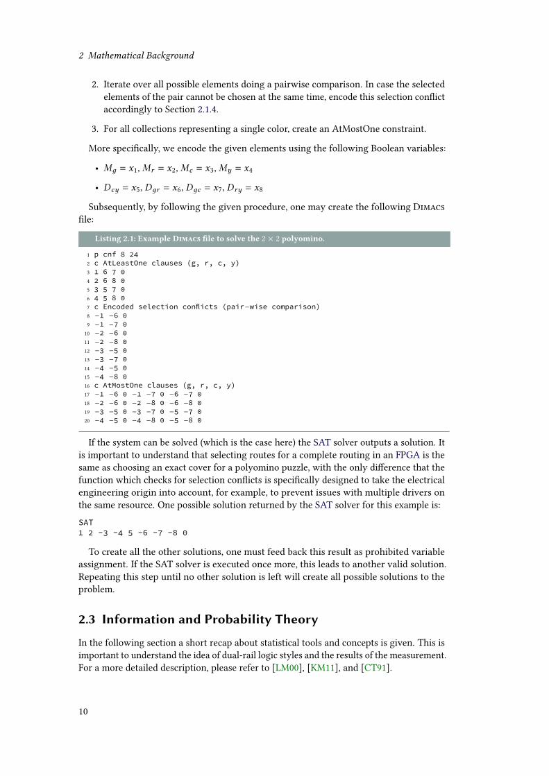
More specifically, we encode the given elements using the following Boolean variables:
• Mд = x1,Mr = x2,Mc = x3,My = x4
• Dcy = x5, Dдr = x6, Dдc = x7, Dry = x8
Subsequently, by following the given procedure, one may create the following Dimacs
file:
Listing 2.1: Example Dimacs file to solve the 2 × 2 polyomino.
1 p cnf 8 242 c AtLeastOne clauses (g, r, c, y)3 1 6 7 04 2 6 8 05 3 5 7 06 4 5 8 07 c Encoded selection conflicts (pair−wise comparison)8 −1 −6 09 −1 −7 010 −2 −6 011 −2 −8 012 −3 −5 013 −3 −7 014 −4 −5 015 −4 −8 016 c AtMostOne clauses (g, r, c, y)17 −1 −6 0 −1 −7 0 −6 −7 018 −2 −6 0 −2 −8 0 −6 −8 019 −3 −5 0 −3 −7 0 −5 −7 020 −4 −5 0 −4 −8 0 −5 −8 0
If the system can be solved (which is the case here) the SAT solver outputs a solution. It
is important to understand that selecting routes for a complete routing in an FPGA is the
same as choosing an exact cover for a polyomino puzzle, with the only difference that the
function which checks for selection conflicts is specifically designed to take the electrical
engineering origin into account, for example, to prevent issues with multiple drivers on
the same resource. One possible solution returned by the SAT solver for this example is:
SAT1 2 -3 -4 5 -6 -7 -8 0
To create all the other solutions, one must feed back this result as prohibited variable
assignment. If the SAT solver is executed once more, this leads to another valid solution.
Repeating this step until no other solution is left will create all possible solutions to the
problem.
2.3 Information and Probability Theory
In the following section a short recap about statistical tools and concepts is given. This is
important to understand the idea of dual-rail logic styles and the results of the measurement.
For a more detailed description, please refer to [LM00], [KM11], and [CT91].
10

2.3 Information and Probability Theory
2.3.1 Probability Space
The probability space can be viewed as a mathematical construct that models the data of
an experiment that consists of events which occur randomly. It is denoted as the triple
(Ω, F , P ) and is defined as follows:
1. Ω is the sample space and contains all possible outcomes.
2. F is a set of events containing zero or more outcomes.
3. P is the function that maps from events to actual probabilities. P : F → R
2.3.2 Discrete Random Variable and Expected Value
The expected value describes the average value of a future experiment by taking the proba-
bility of the occurence into account. Hence, it is a conjecture about the possible outcome.
It can be calculated as:
E(x ) = µ =ni=1
xi · p (xi ) (2.1)
whereas p (xi ) is the probability function. This probability function is defined as:
p (xi ) = P (X = xi ) with
i
p (xi ) = 1
Here, X denotes a discrete random variable and xi the members of X . The sum of all
probabilities is 1.
2.3.3 Variance and Standard Deviation
The variance is a metric to measure how far a set of numbers is spread apart from the
expected value. It is defined as:
var(x ) = σ 2 = E[(x − E(x )]2 (2.2)
= E[x2] − E[x]2 (2.3)
Another term commonly encountered is the standard deviation σ , which is the square
root of the variance. It is used as an easy interpretation of the variance. Its use case is
to define confidence intervals such as [µ − σ , µ + σ ] that are used to indicate how many
samples (as percent) are within a given range. The standard deviation therefore shows how
much variation exists from the expected value.
If this value is small, the observed data is very close to the actual expected value. If it is
large, the observed data is less likely, since its difference from the expected value is large.
11

2 Mathematical Background
2.3.4 Covariance and Correlation Coefficient
The covariance is closely related to the variance and standard deviation. It is used to
measure how much two random variables change together. The meaning of the covariance
is as follows: If two random variables change together, whereas greater values of one
variable correspond with greater values of the other variable, then there is a positive linear
relationship (the covariance is positive). In the opposite case, when greater values of one
variable correspond with smaller values of the other variable, then there is a negative linear
relationship. The covariance is zero if there is no linear relationship. The covariance is
defined as
cov(x ,y) = E[(x − E[x]) (y − E[y])] (2.4)
= E[xy] − E[x]E[y] (2.5)
which is equal to the variance if both variables are the same. The problem of the
covariance is that it is not easy to interpret its magnitude. To better interpret the result,
the normalized version of the covariance, the correlation coefficient is used. Its magnitude
is in the interval [−1, 1] and defined as
corr(x ,y) =cov(x ,y)
var(x ) · var(y)
A high correlation is indicated by values close to 1 or −1. A value close to 0 indicates that
no linear dependency exists, which does not imply that there is no relationship between
the two random variables.
The correlation coefficient is one of the most important tools to analyze recorded power
traces from Devices Under Test (DUTs). Here, the two variables being compared are the
recorded values from the power trace and simulated values. These simulated values are
created by applying a key hypothesis to known input data which is modeled using some
power model (e.g., using the hamming distance). If both simulated values and recorded
data correlate, it is likely that the key hypothesis is correct.
2.3.5 Entropy and Mutual Information
The information theory was developed by Claude E. Shannon to find out about fundamental
principles and limits of signal processing, data compression, and related subjects. In this
context, entropy is used as a measure of the uncertainty in a random variable. It therefore
allows to determine the amount of information in a transmitted message. The entropy is
defined as
H (x ) = Ex [I (x )] = −x
p (x ) log2p (x )
which is the expected value over the self-information I (x ). This definition can be extendedto a conditional entropy, which considers the entropy of a random variable, given another
random variable. The reduction in uncertainty due to the additionally given variable is
called the mutual information. It is defined as:
I (x ,y) = H (x ) − H (x |y) = H (y) − H (y |x ) =x ,y
p (x ,y) log2
p (x ,y)
p (x )p (y)
12
2.3 Information and Probability Theory
It is used as a measure of dependence between the two random variables. Based on its
definition, it can be seen that it is symmetric and always non-negative.
The concept of mutual information can be applied to either observe a reduction in
uncertainty with regards to a given key hypothesis (Mutual Information Analysis, [Bat+11])
or to quantify the relevant leakage apart from a key hypothesis [MSQ07; SMY09] which is
especially of interest for custom (secure) logic styles.
13

3 Technical Background
The following sections are a brief summary of the technical background required to help
understand the implementation and goals of this thesis. The first section in this chapter
deals with FPGAs directly and explains their hardware architecture, software development
flow, and various other interesting aspects. Afterwards, the routing architecture of a
Virtex-5 is described in detail.
In Section 3.3, the Xilinx Description Language (XDL) is described, an intermediate
language used to express possibly placed and routed netlists as an ASCII file. Hereafter, an
introduction to SCA is given to understand the increased security level of specific logic
styles that are presented in Section 3.4.
3.1 FPGAs
The so called FPGAs are a certain type of a reprogrammable integrated circuit. Unlike
ASICs that have a fixed logic elements and wiring do FPGAs have a flexible hardware
architecture consisting of Configurable Logic Blocks (CLBs) and programmable routing
resources. By making use of these CLBs and programmable routing resources, it is possible
to implement even complex hardware functions. When being manufactured, an FPGA only
contains the raw hardware structure without any useful program (called configuration).Later on, this configuration is then written to the FPGA by the developer. Alternatively,
some automated programming procedure is used to configure the FPGA during each power
up, as most FPGAs are volatile and do not preserve their configuration when being powered
off. Configuration can also be done partially on-the-fly which is known as dynamic partial
reconfiguration [HSH09].
3.1.1 Architecture of FPGAs
FPGAs comprise a highly regular grid consisting of generic functional elements. For Xilinx
FPGAs this grid consists of tiles, whereas most tiles contain a global and local routing
switch box and two slices (and some smaller fabrics we do not consider for now). FPGAs
from different manufacturers may use very similar structures. Another tile type may
either feature a Block Random Access Memory (BRAM) or a Digital Signal Processor (DSP).
This architecture type is usually referred to as the “island” style architecture due to its
interconnect structure.
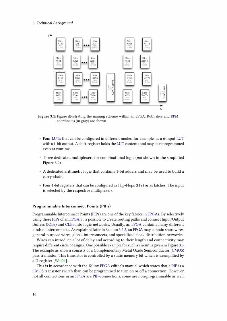
These tiles are arranged in a grid using x and y coordinates, as shown in Figure 3.1. Each
tile also contains primitive sites, for example, Slice X1Y0 is a primitive site of a tile.
Xilinx Virtex-5 Slices
The most dominant component in FPGAs are the CLBs that contain two so called slices.These slices as shown in Figure 3.2 include:
15
3 Technical Background
SliceX0Y0RPM[X9Y0]
SliceX1Y0RPM
[X11Y0]
SliceX2Y0RPM
[X13Y0]
SliceX3Y0RPM
[X15Y0]
SliceX6Y0RPM
[X21Y0]
SliceX7Y0RPM
[X23Y0]
RAMB36_X0Y0RPM
[X25Y0]
SliceX8Y0RPM
[X29Y0]
SliceX9Y0RPM
[X31Y0]
SliceX10Y0RPM
[X33Y0]
SliceX11Y0RPM
[X35Y0]
DSP48_X0Y0
RPM[X37Y0]
SliceX0Y1RPM[X9Y2]
SliceX1Y1RPM
[X11Y2]
SliceX2Y1RPM
[X13Y2]
SliceX3Y1RPM
[X15Y2]
SliceX6Y1RPM
[X21Y2]
SliceX7Y1RPM
[X23Y2]
SliceX8Y1RPM
[X29Y2]
SliceX9Y1RPM
[X31Y2]
SliceX10Y1RPM
[X33Y2]
SliceX11Y1RPM
[X35Y2]
Y
X
Figure 3.1: Figure illustrating the naming scheme within an FPGA. Both slice and RPM
coordinates (in gray) are shown.
• Four LUTs that can be configured in different modes, for example, as a 6-input LUT
with a 1-bit output. A shift-register holds the LUT contents andmay be reprogrammed
even at runtime.
• Three dedicated multiplexers for combinational logic (not shown in the simplified
Figure 3.2)
• A dedicated arithmetic logic that contains 1-bit adders and may be used to build a
carry-chain.
• Four 1-bit registers that can be configured as Flip-Flops (FFs) or as latches. The input
is selected by the respective multiplexers.
Programmable Interconnect Points (PIPs)
Programmable Interconnect Points (PIPs) are one of the key fabrics in FPGAs. By selectively
using these PIPs of an FPGA, it is possible to create routing paths and connect Input/Output
Buffers (IOBs) and CLBs into logic networks. Usually, an FPGA contains many different
kinds of interconnects. As explained later in Section 3.2.2, an FPGAmay contain short wires,
general-purpose wires, global interconnects, and specialized clock distribution networks.
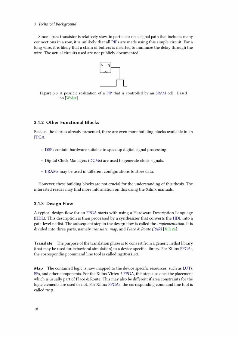
Wires can introduce a lot of delay and according to their length and connectivity may
require different circuit designs. One possible example for such a circuit is given in Figure 3.3.
The example as shown consists of a Complementary Metal Oxide Semiconductor (CMOS)
pass transistor. This transistor is controlled by a static memory bit which is exemplified by
a D register [Wol04].
This is in accordance with the Xilinx FPGA editor’s manual which states that a PIP is a
CMOS transistor switch than can be programmed to turn on or off a connection. However,
not all connections in an FPGA are PIP-connections, some are non-programmable as well.
16

3.1 FPGAs
Arithmeticand
carry logic
LUT
FF
F7CYXORO5O6
F7CYXORAXO5O6
A1A2A3A4A5A6
O6O5 A
AMUXAQ
LUT
FF
F7CYXORO5O6
F7CYXORAXO5O6
B1B2B3B4B5B6
O6O5 B
BMUXBQ
LUT
FF
F7CYXORO5O6
F7CYXORAXO5O6
C1C2C3C4C5C6
O6O5 C
CMUXCQ
LUT
FF
F7CYXORO5O6
F7CYXORAXO5O6
D1D2D3D4D5D6
O6O5 D
DMUXDQ
D Q
D Q
D Q
D Q
Figure 3.2: A simplified diagram of a Xilinx Virtex-5 slice.
17
3 Technical Background
Since a pass transistor is relatively slow, in particular on a signal path that includes many
connections in a row, it is unlikely that all PIPs are made using this simple circuit. For a
long wire, it is likely that a chain of buffers is inserted to minimize the delay through the
wire. The actual circuits used are not publicly documented.
D Q
Figure 3.3: A possible realization of a PIP that is controlled by an SRAM cell. Based
on [Wol04].
3.1.2 Other Functional Blocks
Besides the fabrics already presented, there are even more building blocks available in an
FPGA:
• DSPs contain hardware suitable to speedup digital signal processing.
• Digital Clock Managers (DCMs) are used to generate clock signals.
• BRAMs may be used in different configurations to store data.
However, these building blocks are not crucial for the understanding of this thesis. The
interested reader may find more information on this using the Xilinx manuals.
3.1.3 Design Flow
A typical design flow for an FPGA starts with using a Hardware Description Language
(HDL). This description is then processed by a synthesizer that converts the HDL into a
gate-level netlist. The subsequent step in the design flow is called the implementation. It isdivided into three parts, namely translate, map, and Place & Route (PAR) [Xil12a].
Translate The purpose of the translation phase is to convert from a generic netlist library
(that may be used for behavioral simulation) to a device specific library. For Xilinx FPGAs,
the corresponding command line tool is called ngdbuild.
Map The contained logic is now mapped to the device specific resources, such as LUTs,
FFs, and other components. For the Xilinx Virtex-5 FPGA, this step also does the placement
which is usually part of Place & Route. This may also be different if area constraints for the
logic elements are used or not. For Xilinx FPGAs, the corresponding command line tool is
called map.
18
3.1 FPGAs
PAR After the aforementioned steps, the final and most time consuming step is to ac-
tually place and route the design. This may be done accordingly to different metrics (e.g.,
resource-driven or timing-driven) and may be influenced by constraints set by the deve-
loper to meet certain criteria. PAR defines how the resources are allocated and how they
are interconnected, using the switch-boxes and different wire-types. The corresponding
command line tool is called par.
After the design has been implemented, it is necessary to create a file that can be
understood by the target device. For Xilinx FPGAs this is either a bitstream file or a
Platform Read-Only Memory (PROM) file, depending on whether the FPGA is programmed
via JTAG or from a platform flash. The corresponding Xilinx tools to create these are
bitgen and promgen.
3.1.4 Routing Algorithms and Metrics
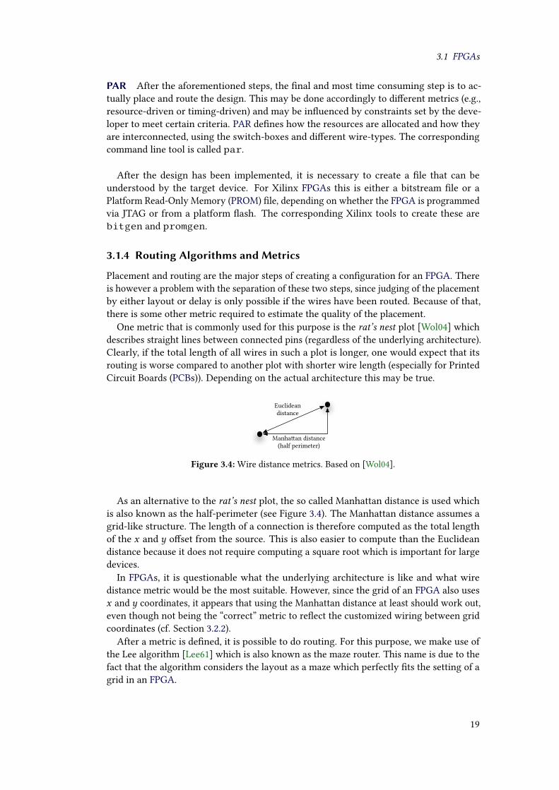
Placement and routing are the major steps of creating a configuration for an FPGA. There
is however a problem with the separation of these two steps, since judging of the placement
by either layout or delay is only possible if the wires have been routed. Because of that,
there is some other metric required to estimate the quality of the placement.
One metric that is commonly used for this purpose is the rat’s nest plot [Wol04] which
describes straight lines between connected pins (regardless of the underlying architecture).
Clearly, if the total length of all wires in such a plot is longer, one would expect that its
routing is worse compared to another plot with shorter wire length (especially for Printed
Circuit Boards (PCBs)). Depending on the actual architecture this may be true.
Euclideandistance
Manhaan distance(half perimeter)
Figure 3.4: Wire distance metrics. Based on [Wol04].
As an alternative to the rat’s nest plot, the so called Manhattan distance is used which
is also known as the half-perimeter (see Figure 3.4). The Manhattan distance assumes a
grid-like structure. The length of a connection is therefore computed as the total length
of the x and y offset from the source. This is also easier to compute than the Euclidean
distance because it does not require computing a square root which is important for large
devices.
In FPGAs, it is questionable what the underlying architecture is like and what wire
distance metric would be the most suitable. However, since the grid of an FPGA also uses
x and y coordinates, it appears that using the Manhattan distance at least should work out,
even though not being the “correct” metric to reflect the customized wiring between grid
coordinates (cf. Section 3.2.2).
After a metric is defined, it is possible to do routing. For this purpose, we make use of
the Lee algorithm [Lee61] which is also known as the maze router. This name is due to the
fact that the algorithm considers the layout as a maze which perfectly fits the setting of a
grid in an FPGA.
19
3 Technical Background
• Advantages: It is guaranteed to find a connection between 2 terminals if such a
connection exists, whereas the connection found is guaranteed to be the minimum
path.
• Disadvantages: The time and space complexity for anm × n grid is O (mn) whichusually results in a slow execution time.
Algorithm 3.1.1: Lee Algorithm [Lee61], algorithm description from [Wik13]
1 begin
/* Initilization */2 Select start point, mark with 0
3 i := 0
/* Filling or Wave Propagation Phase */4 repeat
5 Mark all unlabeled neighbors of points marked with i with i+1
6 i := i+1
7 until (target reached) or (no points can be marked)/* Retrace or Backtrace Phase */
8 go to the target point repeat
9 go to next node that has a lower mark than the actual node
10 add this node to path
11 until (start point reached)/* Label Clearance */
12 Block the path for future wirings
13 Delete all marks
3.2 Xilinx Virtex 5 Routing Architecture
Public information on the Xilinx FPGA routing architecture is scarce. The best information
from Xilinx that can be found is the “Virtex-5 Platform FPGA Family Technical Back-
grounder” [Xil06]. Despite its name, it contains only very few details about the internal
architecture of the FPGA.
The RapidSmithmanual [Lav+12] also does not include any information about the routing
architecture and we can only assume that the following pieces of information are known to
the authors but did not make it into the manual. The accumulated findings have therefore
been put together to serve as a future reference.
3.2.1 Overview
The routing interconnect architecture of the Virtex-5 is a diagonally symmetric pattern
as shown in Figure 3.5. While the number of hops is not explained in the aforementioned
document, it is easily understood when having a look at the figures provided in Section A.1.
In this context, a hop is understood as the single wiring segment that is used for setting up
a link between two logic blocks, no matter if they are neighboring or not.
Unlike its predecessor, the routing architecture is more comprehensive, allowing more
logic connections. The exact numbers are given in Table 3.1.
20
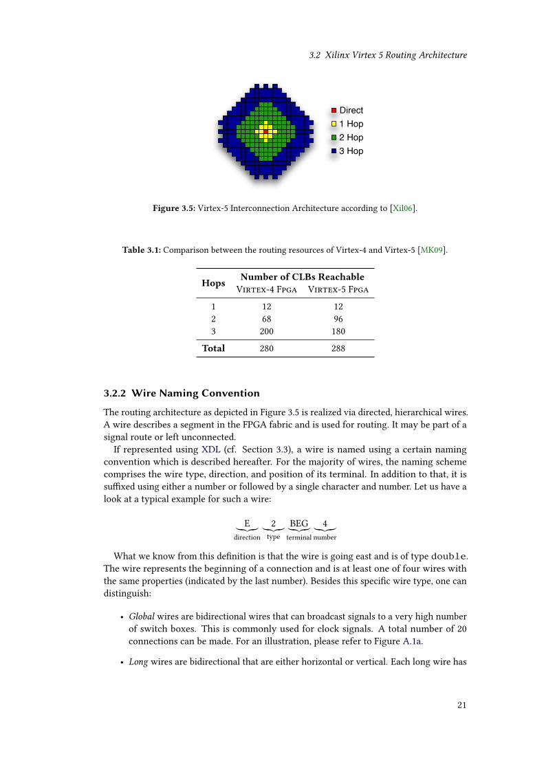
3.2 Xilinx Virtex 5 Routing Architecture
Direct1 Hop2 Hop3 Hop
Figure 3.5: Virtex-5 Interconnection Architecture according to [Xil06].
Table 3.1: Comparison between the routing resources of Virtex-4 and Virtex-5 [MK09].
Hops
Number of CLBs Reachable
Virtex-4 Fpga Virtex-5 Fpga
1 12 12
2 68 96
3 200 180
Total 280 288
3.2.2 Wire Naming Convention
The routing architecture as depicted in Figure 3.5 is realized via directed, hierarchical wires.
A wire describes a segment in the FPGA fabric and is used for routing. It may be part of a
signal route or left unconnected.
If represented using XDL (cf. Section 3.3), a wire is named using a certain naming
convention which is described hereafter. For the majority of wires, the naming scheme
comprises the wire type, direction, and position of its terminal. In addition to that, it is
suffixed using either a number or followed by a single character and number. Let us have a
look at a typical example for such a wire:
Edirection
2type
BEGterminal
4number
What we know from this definition is that the wire is going east and is of type double.The wire represents the beginning of a connection and is at least one of four wires with
the same properties (indicated by the last number). Besides this specific wire type, one can
distinguish:
• Global wires are bidirectional wires that can broadcast signals to a very high number
of switch boxes. This is commonly used for clock signals. A total number of 20
connections can be made. For an illustration, please refer to Figure A.1a.
• Long wires are bidirectional that are either horizontal or vertical. Each long wire has
21

3 Technical Background
4 connections. This wire is used for large distance signals. For an illustration, please
refer to Figure A.1b.
• Pent(anomial) wires, are unidirectional wires that span a distance of 5, whereas the
Manhattan distance is applied. Each wire interconnects 3 switch boxes. Both straight
and diagonal connections are made, as can be seen in Figure A.2.
• Double wires are bidirectional wires that span a distance of 2, whereas the Manhattan
distance is applied. Each wire interconnects 3 switch boxes. Both straight and
diagonal connections are made, as can be seen in Figure A.3.
• Additional wires types:
– Bounceacross wires are unidirectional wires that connect to the neighboring
switch box.
– Turn wires describe either double or pent wires that make a turn.
– Other wire types without specific group occur within each switch box, for
example, INT_SINK, INT_SOURCE and INT_CONN. This list is incomplete.
An abstract illustration of these wires can be found when viewing the Native Circuit
Description (NCD) of a design by using the Xilinx FPGA editor. A screenshot of this view
is shown in Figure 3.6.
However, not all of these wires types follow the presented naming scheme. For those in
accordance with the naming scheme, we present a partial list of the possible properties:
• Direction: (N) north, (NE) north east, (E) east, (SE) south east, . . .
• Type: 2 = double, 5 = pent, L = long, . . .
• Terminal: For unidirectional wire types, the terminal indicates whether the pro-
grammed connection is the starting point or one of the destinations. The only
allowed values are: BEG (beginning), MID (middle), END (end).
• Character/Number: If there is more than one wire available in the same direction, a
number is used to indicate the actual wire. The sum of all wires going in the same
direction is called a wiring channel. Alternatively, the suffix _N2 is used to indicate a
turn wire.
For wire types not following this naming scheme, we are now presenting a few examples.
We should note, that we already describe these wires as PIP of the FPGA. This is denoted
by using the arrow -> as shown below.
• PIP connection from a LUT output to a local output via a multiplexor:
L_A -> L_AMUX
• PIP connection from a double wire to an input multiplexor of a switch box:
NW2MID2 -> IMUX_B29
• PIP connection between two switch box internal connections (presumably bypass?):BYP6 -> BYP_BOUNCE6
• Various other examples:
22

3.2 Xilinx Virtex 5 Routing Architecture
5
6
4
32
1
7
8
9
Figure 3.6: This screenshot taken from the Xilinx FPGA editor shows two tiles each with
their corresponding switch box and pair of slices. The numbers assigned are:
1 pent wires 2 double wires 3 bounceacross wires 4 horizontal long wires
5 global wires 6 vertical long wires 7 global switch box 8 local switch box
9 slices
23

3 Technical Background
– CTRL2 -> CTRL_BOUNCE2
– FAN2 -> FAN_BOUNCE2
Since there is no public documentation at hand, one can only speculate about the actual
name used and the circuit representing the wire or specific connection. What is known
for sure that different wire types have different properties, for example, the slew rate and
drive strength.
If the wire occurs within an XDL file, it is always prefixed with the word “pip”, indicating
that it is indeed a PIP connection. However, many connections in an FPGA exist that are
non-programmable. These implicit connections cannot be found in an XDL file since the
original tools prohibit to create or convert such a file.
Figure 3.7: Example illustrating almost all possible interconnects within an FPGA switch
box. Each line is representing a possible interconnect. Using the Xilinx FPGA
editor, yellow and purple lines are used to distinguish between incoming and
outgoing connections. Clearly visible are the bounce wires that get redirected.
3.2.3 Xilinx Routing and DIRTs
For existing connections, or connections manually routed using the FPGA editor, Xilinx
allows to save the routing information. This can be done using DIRTs and is intended for
highly critical signals but only works for completely routed nets (partially routed nets did
not work in our tests). Using this workflow, it is possible to refactor the User Constraint
File (UCF) to contain the necessary information. In subsequent routing attempts, the fixed
route is then used. As an example, we analyze one of the nets shown in Figure 4.8. This net
has a source and two sinks.
ROUTE="3;1;5vlx50ff324;9d768b2d!-1;-67720;-187632;S!0;0;-8!1;-843;-464!""2;2683;-433!3;1469;849!3;1469;561!4;843;88;L!5;843;272;L!";
Unfortunately, no information can be found about the syntax of this constraint. Due
to that, it is not possible to enhance the routing in an automated manner using these
commands. However, by analyzing the structure of this command, we see that it can be
reformatted (omitting the quotes, presumably indicating a line break). After reformatting,
a clear structure can be deduced.
24

3.2 Xilinx Virtex 5 Routing Architecture
ROUTE="3;1;5vlx50ff324;9d768b2d! -1; -67720; -187632;S! 0; 0; -8! 1; -843; -464! 2; 2683; -433! 3; 1469; 849! 3; 1469; 561! 4; 843; 88;L! 5; 843; 272;L!";
While the first line indicates the speed grade, family name, package, and some magic
string (presumably indicating a location constraint), it is evident that the following lines
comprise the actual routing. Each line starts with an exclamation mark followed by three
columns separated via semicolons. The first column appears to contain a counter that is
incremented.
To better understand the next two columns, it is necessary to have a look at the specific
route using the FPGA editor. When hovering the cursor over specific segments of the route
some extra information is displayed, such as the following:
net"mu<0>", node=OUTPUT(-67720,187640)
This can be done for all segments of a route:
net"mu<0>", arc=OUTPUT(-67720,187640) --> OUTBOUND(-68563,-188104)net"mu<0>", node=OUTBOUND(-68563,188104)net"mu<0>", arc=OUTPUT(-68563,188104) --> DOUBLE(-65880,-188537)net"mu<0>", node=DOUBLE(-65880,-188537)
Now the signal arrives at the final switch box and splits to connect to the two sink pins.
Hovering the cursor over one of the two connection yields
net"mu<0>", arc=DOUBLE(-65880,-188537) --> PINFEED(-64411,-187688)net"mu<0>", node=PINFEED(-64411,-187688)net"mu<0>", arc=PINFEED(-64411,-187688) --> INPUT(-63568,-187600)
and for the other connection:
net"mu<0>", arc=DOUBLE(-65880,-188537) --> PINFEED(-64411,-187976)net"mu<0>", node=PINFEED(-64411,-187976)net"mu<0>", arc=PINFEED(-64411,-187976) --> INPUT(-63568,-187704)
After looking at these numbers for a while, it is striking that the differences between
subsequent nodes are the numbers contained in the DIRT. This is demonstrated in Tables 3.2
and 3.3.
It follows, that the first entry can be seen as the depth of the route and the next two
columns as coordinates x and y. For the source of the route, a capital s indicates the startof the route, whereas a capital l indicates a sink pin.
We have analyzed the DIRT constraint and know how the routing is realized by using
routes with x and y coordinates. For practical use, this interface is too cumbersome and
an easier approach is required. Because of that, we make use of the tool RapidSmith as
explained in Chapter 4.
25
3 Technical Background
Table 3.2: Small computation to ex-
plain how DIRTs work.
This example is for one of
the two sink pins of a net.
Level x y
-67720 -187632
0 0 -8
-67720 -187640
1 -843 -464
-68563 -188104
2 2683 -433
-65880 -188537
3 1469 849
-64411 -187688
4 843 88
-63568 -187600
Table 3.3: Small computation to ex-
plain how DIRTs work.
This example is for one of
the two sink pins of a net.
Level x y
-67720 -187632
0 0 -8
-67720 -187640
1 -843 -464
-68563 -188104
2 2683 -433
-65880 -188537
3 1469 561
-64411 -187976
5 843 272
-63568 -187704
3.3 XDL – Xilinx Design Language
XDL is a text-based language developed by Xilinx to describe the FPGA configuration.
This description comprises the exact slice configuration and routing information. It is a
powerful interface that allows to arbitrarily modify the FPGA contents, possibly exceeding
the options offered by Xilinx ISE. Unfortunately, XDL is not officially supported by Xilinx
and future support is doubtful.
3.3.1 XDL Files
The only official documentation available for XDL files are the verbose syntax comments
within the files. The basic structure of an XDL file consists of three statements: the design
statement, the module statement, and the instance statement.
Design Statement
If generated by the Xilinx tools, an XDL file starts with the design statement which includes
global information such as the design and part name. In addition to that, it contains a list
of attributes in a ’cfg’ string. These attributes describe various other design properties, for
example, a timestamp of the design. The design statement is always part of an XDL file
and is represented in RapidSmith by the class Design. The syntax of this statement and a
tiny example are given hereafter:
# =======================================================# The syntax for the design statement is:# design <design_name> <part> <ncd version>;# or# design <design_name> <device> <package> <speed> <ncd_version># =======================================================design "present" xc5vlx50ff324-1 v3.2 ,
26
3.3 XDL – Xilinx Design Language
cfg "_DESIGN_PROP::BUS_INFO:4:INPUT:data_in<3:0>_DESIGN_PROP::BUS_INFO:4:INPUT:data_mask_m<3:0>_DESIGN_PROP::BUS_INFO:4:INPUT:data_mask_n<3:0>_DESIGN_PROP::BUS_INFO:4:INPUT:key<3:0>
...
Instance Statement
The instance statement occurs very often in an XDL file and describes the instance of an
FPGA primitive. In case a primitive site and location are specified, the primitive is placed.
If not, it is unplaced. Of course, for a finished design, we assume that every instance is
placed. Each instance also has a primitive type, such as SLICEL and SLICEM.The RapidSmith report states that instance names should be unique to avoid possible
conflicts. If the file is generated from a properlyworking VHSIC (VeryHigh Speed Integrated
Circuit) Hardware Description Language (VHDL), this should never happen. The syntax of
the command is given below.
# =======================================================# The syntax for instances is:# instance <name> <sitedef>, placed <tile> <site>, cfg <string> ;# or# instance <name> <sitedef>, unplaced, cfg <string> ;## For typing convenience you can abbreviate instance to inst.## For IOs there are two special keywords: bonded and unbonded# that can be used to designate whether the PAD of an unplaced IO is# bonded out. If neither keyword is specified, bonded is assumed.## The bonding of placed IOs is determined by the site they are placed in.## If you specify bonded or unbonded for an instance that is not an# IOB it is ignored.## Shown below are three examples for IOs.# instance IO1 IOB, unplaced ; # This will be bonded# instance IO1 IOB, unplaced bonded ; # This will be bonded# instance IO1 IOB, unplaced unbonded ; # This will be unbonded# =======================================================
The following example is the instance statement of a logic element used in one of our
designs. If carefully read, it can be seen that two LUTs are instantiated and two FFs.
inst "Inst_aestiny/SBOX/ins89/XORPACK_FF" "SLICEL",placed CLBLM_X13Y7 SLICE_X21Y7,cfg " A5LUT::#OFFA6LUT:Inst_aestiny/SBOX/ins89/TruePart:#LUT:O6=((~A1*((~A2*(((~A3*A4)+A3)*A5))+(A2*(A3+A5))))+(A1*((~A2*(A4+A5))+(A2*(A3+(A4+A5))))))
_BEL_PROP::A6LUT:BEL:A6LUT ACY0::#OFF AFF:Inst_aestiny/SBOX/ins89/FDRSE_TruePart:#FF
_BEL_PROP::AFF:BEL:AFF AFFINIT::INIT0 AFFMUX::O6 AFFSR::SRLOW AOUTMUX::#OFFAUSED::0 B5LUT::#OFF
B6LUT: Inst_aestiny/SBOX/ins89/FalsePart:#LUT:O6=((~A1*((~A2*(((~A3*A4)+A3)*A5))+(A2*(A4+A5))))
+(A1*((~A2*(A3+A5))+(A2*(A3+(A4+A5))))))
27

3 Technical Background
_BEL_PROP::B6LUT:BEL:B6LUT BCY0::#OFFBFF:Inst_aestiny/SBOX/ins89/FDRSE_FalsePart:#FF
_BEL_PROP::BFF:BEL:BFF BFFINIT::INIT0 BFFMUX::O6 BFFSR::SRLOW BOUTMUX::#OFFBUSED::0 C5LUT::#OFF C6LUT::#OFF CCY0::#OFF CEUSED::0 CFF::#OFF CFFINIT::#OFFCFFMUX::#OFF CFFSR::#OFF CLKINV::CLK COUTMUX::#OFF COUTUSED::#OFFCUSED::#OFF D5LUT::#OFF D6LUT::#OFF DCY0::#OFF DFF::#OFF DFFINIT::#OFFDFFMUX::#OFF DFFSR::#OFF DOUTMUX::#OFF DUSED::#OFF PRECYINIT::#OFFREVUSED::#OFF SRUSED::#OFF SYNC_ATTR::SYNC "
;
Net Statement
The net statement describes the actual routing and contains a list of all PIP connections.
The chosen name for a net must be unique among all nets. Each net also contains a list
of pins that can either be a source (only single pin per net) or a sink (multiple pins per
net). The name of the pin must be unique and is defined by the name of its instance as well
as the internal name of the pin on this particular instance. Depending on whether it is a
source or sink pin, it is named outpin or inpin respectively.
For all PIP connections, the default wire type is assumed (which is simply “wire”). The
naming scheme has already been explained beforehand in Section 3.2.2. Each PIP connection
is preceded by the keyword pip and the name of the tile where it resides. For two tiles, we
now explain the naming scheme and meaning:
• The tile CLBLt_XnYm contains all PIPs that are connecting from the switch box to
the actual slice, whereas t is either L or M for the specific slice type. The x and ycoordinates are given as numbers and put in place of n andm. This type of tile is
used for wires between or within global switch boxes.
• The tile INT_XnYm contains all PIPs that connect from either the global switch box to
the local switch box, or from the local switch box to the slices.
It follows the syntax description as found in an XDL file:
# ================================================# The syntax for nets is:# net <name> <type>,# outpin <inst_name> <inst_pin>,# .# .# inpin <inst_name> <inst_pin>,# .# .# pip <tile> <wire0> <dir> <wire1> , # [<rt>]# .# .# ;## There are three available wire types: wire, power and ground.# If no type is specified, wire is assumed.## Wire indicates that this a normal wire.# Power indicates that this net is tied to a DC power source.# You can use "power", "vcc" or "vdd" to specify a power net.#
28

3.3 XDL – Xilinx Design Language
# Ground indicates that this net is tied to ground.# You can use "ground", or "gnd" to specify a ground net.## The <dir> token will be one of the following:## Symbol Description# ====== ==========================================# == Bidirectional, unbuffered.# => Bidirectional, buffered in one direction.# =- Bidirectional, buffered in both directions.# -> Directional, buffered.## No pips exist for unrouted nets.# ================================================
For the example that will be given shortly, we may also use the Xilinx FPGA editor to
illustrate it. As shown in Figure 3.8, the example contains two connections that connect
from one slice to another.
Figure 3.8: Example of a well-balanced dual-rail signal from one slice to another.
The XDL code for this example is:
• net m<1>:outpin "m<1>" B ,inpin "out2_1_OBUF" A2 ,inpin "out2_1_OBUF" B2 ,pip CLBLL_X4Y0 SITE_IMUX_B4 -> L_A2 ,pip INT_X4Y0 SR2BEG2 -> IMUX_B4 ,pip INT_X4Y0 EL2END2 -> SR2BEG2 ,pip INT_X2Y0 EN2MID2 -> EL2BEG2 ,pip INT_X1Y0 LOGIC_OUTS17 -> EN2BEG2 ,pip CLBLM_X1Y0 L_BMUX -> SITE_LOGIC_OUTS17 ,pip CLBLM_X1Y0 L_B -> L_BMUX ,pip CLBLL_X4Y0 SITE_IMUX_B40 -> L_B2 ,pip INT_X4Y0 SR2BEG2 -> IMUX_B40 ,
• net m<0>:outpin "m<0>" A ,inpin "out2_1_OBUF" A1 ,inpin "out2_1_OBUF" B1 ,pip CLBLL_X4Y0 SITE_IMUX_B5 -> L_A1 ,pip INT_X4Y0 FAN_BOUNCE5 -> IMUX_B5 ,pip INT_X4Y0 FAN5 -> FAN_BOUNCE5 ,pip INT_X4Y0 ER2END1 -> FAN5 ,pip INT_X2Y0 ES2MID0 -> ER2BEG1 ,pip INT_X1Y0 LOGIC_OUTS8 -> ES2BEG0 ,pip CLBLM_X1Y0 L_A -> SITE_LOGIC_OUTS8 ,pip CLBLL_X4Y0 SITE_IMUX_B41 -> L_B1 ,pip INT_X4Y0 FAN_BOUNCE5 -> IMUX_B41 ,
29

3 Technical Background
Please note that the order of the PIPs in XDL files is arbitrary. To follow one connection
to the next, it is required to completely parse and analyze the structure, especially to
detect implicit (non-programmable) connections as well. An additional note must be made
concerning the use of the -> symbol which in case of RapidSmith is used for long lines,
too. These long lines would otherwise be denoted using the symbol -= (if created by the
original Xilinx tools). This modification however does not cause any problems with the
Xilinx tools and is thus used for simplicity.
Module Statement
The module statement is used to hold collections of instances and nets. This is used to
describe so called hard macros – instances that are are placed and routed. Each module has
a list of ports that define an interface of the hard macro. As for the other statements, the
syntax can be found in the XDL file and we omit it here.
3.3.2 XDLRC Files
XDLRC files represent XDL resource files that provide all the logic and interconnect data
for the FPGAs. XDLRC files are very huge (depending on the actual device used), usually
above multiple gigabytes. The information that can be foud in XDLRC files can be used by
the router to find routes between two given points, or adjacent connections from a single
point. For ease of access, this information has been processed by RapidSmith and is directly
available within the library. Hence, it is not necessary to deal with the original files.
3.3.3 File Format Conversion and Limitations
The previously presented file formats can be generated using the following commands:
• The following command converts a netlist (.ncd) into an XDL file:
xdl -ncd2xdl designName
• The following command converts an XDL file into a netlist (.ncd):xdl -xdl2ncd designName
• The following command creates an XDLRC file:
xdl -report -pips -all_conns partName
The limitations of both XDL and XDLRC files are that there is no contained delay support.
It is therefore not possible to extract any delay information from these file formats. In
addition to that, the syntax does not allow to access units smaller than complete nets. Due
to that, there is no direct approach to describe dual-rail connections within an XDL file
using the given syntax. Additional information about XDL files can be found here [BKT11].
3.4 Secure Logic Styles
SCA has been a threat to cryptographic devices since the first attack was published by Paul
Kocher [KJJ99]. Especially power analysis, which extracts information from recorded power
traces, is in particular useful because the attack itself is non-invasive. Hence, attacking the
device is possible without tampering it.
30

3.4 Secure Logic Styles
To counteract this very powerful type of attack, various proposals have been made. At the
cell level secure logic styles such as WDDL [TV04] and MDPL [PM05] have been proposed
to avoid the dependency of the power consumption of the circuit and the processed data.
However, various research publications have shown that preventing data-dependency is
not enough to thwart side-channel analysis. If a straight-forward implementation of the
logic is used, the number of toggles still will be distinguishable for different input changes.
Hence, a scheme is required that prevents glitches and makes the number of toggles fixed
regardless of the input changes.
With respect to these additional requirements, we present various logic styles. In addition
to that, we do a recap on the foundations of SCA and explain the concept of dual-rail logic
which is a common building block for secure logic styles.
3.4.1 Idea and Concepts of Side-Channel Analysis
The success of power analysis is due to the frequent use of the CMOS technology. This
technology which is well-known for its low power consumption has the disadvantage
(from a security point of view) that the main part of the power consumption only occurs
when the circuit is actually processing data. Because of that, there is a clear dependency
between the power consumption and the intermediate values of a cryptographic device.
This dependency can then be exploited by various attacks, for example, a Correlation Power
Analysis (CPA) (cf. Section 2.3.4) [KM11].
CMOS circuits consist of pull-up and pull-down networks that are constructed in such
a way that they do not conduct at the same time for constant input signals. In this state,
only static currents pass the circuit which are very small compared to the currents due to
dynamic switching behavior. The CMOS inverter as shown in Figure 3.9 is representative
for such a circuit because it is commonly used in CMOS circuits.
GND
CL
VDD
In Out
Figure 3.9: Illustration of a CMOS inverter.
For this example, we analyze the following transitions of the input signal. Depending on
the type of the transition, we either observe a static or a dynamic power consumption:
• 0→ 0, static power consumption
• 0→ 1, static and dynamic power consumption
• 1→ 0, static and dynamic power consumption
• 1→ 1, static power consumption
31

3 Technical Background
This dynamic power behavior is eventually used to mount a successful attack. On top
of that, other effects adversely affect the security of the device. Since designs typically
consist of larger combinatorial circuits where signals do not arrive at the same time, thereby
creating intermediate signals on the output also known as glitches. Even worse, these
glitches cause the subsequent logic elements to create additional glitches that are not related
to the intended input values.
3.4.2 WDDL – Synchronous Secure Logic Style
WDDL [TV04] is one example of a dual-rail logic style that aims at securing cryptographic
operations in circuits. It was specifically designed to use standard cells, therefore avoiding
the hassle of a full-custom design tool. Unlike single-rail logic, each bit is now represented
using two wires. The values of these two wires are denoted as (·,·), whereas in case of
WDDL the only valid values are: (0, 1) and (1, 0).
Because each signal pair is always made from two bits that are the opposite of each other,
the single rails are called true and false rail. This approach requires to use certain gates
to perform the same logical operations on the values. The required gates are depicted in
Figure 3.10b.
(a) Precharge
generation.
(b) Concept of WDDL.
Figure 3.10: Illustration of WDDL gates including precharge generation [TV04].
By using this concept, a full switching activity on both rails is achieved. This is illustrated
in Figure 3.11 by comparing a CMOS NAND gate with a WDDL NAND gate. Beforehand,
a transition clearly leaked information due to the dynamic power consumption. In case of
WDDL this is not the case, as the dynamic power is always ’1’. In a purely mathematical
model, this would lead to a variance of 0, since there is no deviation.
Necessary for the practical and secure use of WDDL is an additional technique known
as DPL. It is used to start new computations from a known electrical state and thereby
prevent unexpected transitions between two computations. During precharge phase (half
a clock cycle, cf. Figure 3.10a), the two wires are initialized with (0, 0). In the evaluation
phase, only one lines goes to HIGH. Because of this scheme, there will be no glitch in the
circuit and the number of toggles will be fixed.
Still, even if both techniques are combined, there is another obstacle: to have a constant
power consumption on both rails, their capacitive loads must be the same. Otherwise, it is
32

3.4 Secure Logic Styles
NAND
Static PowerDynamic Power
1 1 0 1
0 1 1
B
B
A
A
(a) A standard CMOS NAND with data-
dependent power consumption.
AND
OR
10 Static PowerDynamic Power
10 10 101 1 1 1 1 1 1
Bp
Ap
Ap
Bp
Qp
Qp
Ap
Bp
Ap
Bp
Qp
Qp
(b) A DPL NAND with data-independent
power consumption.
Figure 3.11: Comparison of a single-rail and WDDL NAND element in terms of static and
dynamic power consumption. Based on [Sin11]
still possible to distinguish between transitions on one or the other rail. To have a constant
power consumption, the input capacitance of the gates in addition to the capacitance
induced by the routing of the rails must be the same. This can only be realized in ASICs by
using a full custom workflow.
However, even if both rails are perfectly balanced, there are attacks on WDDL possible.
This is due to the early propagation effect [KKT06]. This effect describes the problem with
gates that have an evaluation time that depends on the value of the input, for instance, a
gate that fires the output before all signals have arrived. This can be easily understood
when looking at a logical AND gate. Clearly, if one input to such a gate is 0, the output
instantly changes to 0 once the signal arrives. This time of evaluation is different to the
case when a 1 arrives on both signals.
These differences caused by the early propagation effect and the load mismatches may
also pile up along the combinational circuit. This causes the power consumption to have
different patterns according to different inputs, thereby making a Side Channel Analysis
possible.
3.4.3 Asynchronous Logic Styles
Asynchronous circuits have been favored in the early days of electronic circuits for their
potential to be faster and their lower power consumption. This type of circuit style, also
known as self-timed circuit, does not use a clock signal as it is the case for synchronous
circuits. Instead, handshake protocols are commonly used for data transfers (e.g., 4-phase
asynchronous logic). Though, asynchronous logic is also possible with a fixed initialization
state and without a certain protocol (e.g., 2-phase asynchronous logic) [MC79].
Despite the advantages of asynchronous logic, it is generally assumed that the develop-
ment of synchronous designs is easier in terms of debugging, testing, and the development
process itself. On the one hand, this is due to the lack of support in many commercially
Electronic Design Automation (EDA) tools, one the other hand it is due to the huge variety
of asynchronous logic styles. Especially modern FPGA tools, such as the Xilinx ISE, com-
pletely lack support to analyze asynchronous designs. Because of that are asynchronous
elements such as latches commonly avoided in FPGAs.
With regard to the security requirements of a side-channel resistant implementation, it
is expected that asynchronous logic styles have certain advantages over synchronous logic.
In a recent publication [Cha+11], the advantages are given as follows:
33

3 Technical Background
• Decreased likelihood of successful fault attacks, since randomly inserted faults are
supposed to stall the asynchronous circuit.
• The absence of a time reference (e.g., the clock signal) makes the precise model for
transitions more difficult to predict.
• The absence of glitchesmakes asynchronous circuits more resistant than logic realized
in standard CMOS logic.
In the following subsection, we are going to take a look at AWDDL [MI], a novel logic
style which has so far not been examined for realizing secure cryptographic circuits.
Asynchronous WDDL (AWDDL)
The asynchronous variant of WDDL was designed to prevent the early propagation effect
and follows the WDDL definitions but its time-of-evaluation is independent of the input
values by realizing a self-timed approach. The asynchronous behavior of this logic style is
implemented by using S-R latches. Since the target platform is an FPGA, it is important
how these latches can be realized. This is done by making combinational loops from the
LUT output to one of its inputs. This approach is depicted in Figure 3.12.
At
Af
Bt
Bf
Zt
At
Bt
St
Rt
At
Af
Bt
Bf
0
0
1
2
3
4
5
LUT6-1
S-R
Latch
At
Af
Bt
Bf
Zf
Af
Bf
Sf
Rf
At
Af
Bt
Bf
0
0
1
2
3
4
5
LUT6-1
S-R
Latch
Af
Bt
At
Bf
Figure 3.12: AWDDL AND/NAND gate†[MI].
In this case, the Boolean function must be implemented as a LUT in conjunction with
the S-R latch. Otherwise, if implemented in an ASIC one could exploit technological effects
of the implementation, for example, unbalanced number of toggles.
By following asynchronous design concepts, one is able to derive the formulas for the
set and reset signals of the internal S-R latch of 2-input gates as given below. Like before, a
precharge logic is used to start evaluating the combinational circuit.
†Due to the implementation of the LUT6 instances in the Virtex-5, it should be mentioned that input 4 of the
LUT should be used for the combinational loop (instead of input 5 as shown in the figure above). Input 5
should be set to “1” such that only O6 is used as gate output.
34

3.4 Secure Logic Styles
all gates : Rt = Rf = At + Af + Bt + Bf
AND :
St = At Bt
Sf = Af Bf + Af Bt + At Bf
OR :
St = At Bt + At Bf + Af Bt
Sf = Af Bf
XOR :
St = At Bf + Af Bt
Sf = At Bt + Af Bf
While the logic style does not suffer from the early propagation effect, it is also prone
to imbalanced routing of the dual rails. This is in particular problematic since an FPGA
does not allow to achieve a perfect symmetry between rails, even if the provided tools
would allow such a routing (which is not the case). In addition to that, uncontrolled
placement may additionally affect optimal side-channel resistance. Because of that, every
corresponding LUT that provides the output Zt and Zf should be kept together in a single
slice and therefore as close together as possible.
35


4 Implementation
To realize the various aspects of this thesis, a customized router has been written to fully
automatically route balanced signals. At first, we describe the foundations of the RapidSmith
library in Section 4.1. Afterwards, our customized router and its structure is described in
Section 4.2. In Section 4.3, a description is given on how the secure logic styles have been
implemented in VHDL/Verilog. To find out about a reasonable optimization goal, a small
analysis of the FPGA routing architecture (and its delays) is presented in Section 4.4.
4.1 RapidSmith Library
RapidSmith is a Java library that aims at providing an easy-to-use platform to experiment
with Xilinx FPGAs and their proprietary file formats, namely .xdl and .bit. To present
the customized router later on, it is necessary to detail the structure of RapidSmith first.
4.1.1 Introduction to RapidSmith
The common workflow on how to develop and create the FPGA configuration was in-
troduced in Section 3.1.3. It can be seen that many steps are required to complete a
configuration file. RapidSmith [Lav+12] does not provide a complete toolchain to replace
these steps. Instead, it still relies on vendor tools. More specifically, it only targets the
intermediate steps where an XDL file may be created using the corresponding command
line tool. This idea is depicted in Figure 4.1.
Xilinxmap
Xilinxpar -r
(place only)
Xilinxbitgen
Xilinxxdl
BYU RapidSmith Tools
Xilinxpar -p
(route only)
Xilinxxdl
Xilinxxdl
.NCD .NCD .NCD .BIT
.XDL .XDL .XDL
Figure 4.1: The design flow using RapidSmith in conjunction with Xilinx tools.
Not shown are the steps prior to the mapping, because of the fact they are still carried
37
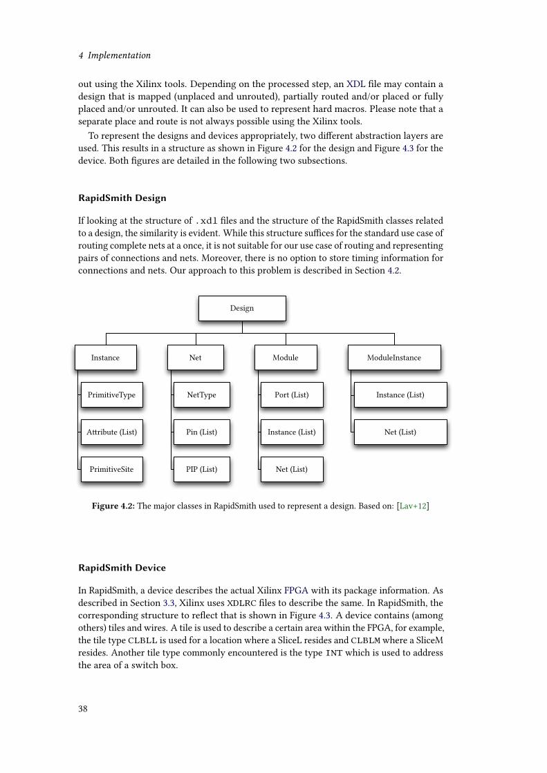
4 Implementation
out using the Xilinx tools. Depending on the processed step, an XDL file may contain a
design that is mapped (unplaced and unrouted), partially routed and/or placed or fully
placed and/or unrouted. It can also be used to represent hard macros. Please note that a
separate place and route is not always possible using the Xilinx tools.
To represent the designs and devices appropriately, two different abstraction layers are
used. This results in a structure as shown in Figure 4.2 for the design and Figure 4.3 for the
device. Both figures are detailed in the following two subsections.
RapidSmith Design
If looking at the structure of .xdl files and the structure of the RapidSmith classes related
to a design, the similarity is evident. While this structure suffices for the standard use case of
routing complete nets at a once, it is not suitable for our use case of routing and representing
pairs of connections and nets. Moreover, there is no option to store timing information for
connections and nets. Our approach to this problem is described in Section 4.2.
Design
Instance Net Module ModuleInstance
PrimitiveType
Aribute (List)
PrimitiveSite
NetType
Pin (List)
PIP (List)
Port (List)
Instance (List)
Net (List)
Instance (List)
Net (List)
Figure 4.2: The major classes in RapidSmith used to represent a design. Based on: [Lav+12]
RapidSmith Device
In RapidSmith, a device describes the actual Xilinx FPGA with its package information. As
described in Section 3.3, Xilinx uses XDLRC files to describe the same. In RapidSmith, the
corresponding structure to reflect that is shown in Figure 4.3. A device contains (among
others) tiles and wires. A tile is used to describe a certain area within the FPGA, for example,
the tile type CLBLL is used for a location where a SliceL resides and CLBLMwhere a SliceM
resides. Another tile type commonly encountered is the type INT which is used to address
the area of a switch box.
38

4.2 Customized Router using RapidSmith
Tile (2D Array)
TileType PrimitiveSite(Array) Wire
PrimitiveType
Tile
Device
Figure 4.3: The major classes in RapidSmith used to represent a device. Based on: [Lav+12]
4.1.2 Routing using RapidSmith
RapidSmith already incorporates various classes to represent wires, connections, and a class
for basic routing. While the basic router serves as a good start for interested developers,
it is by far not suitable to route any real-world designs because it lacks some important
features, such as awareness of routing conflicts, resource usage, and timing constraints.
In addition to that, there is no heuristic that could possibly enhance placing and routing.
This is simply owed to the fact that Xilinx does not release any information about their
internal FPGA architecture.
Wire Representation
To represent wires, a unique representation is derived from the wire naming used in XDLRCfiles. This wire representation is described in detail in Section 3.2.2. For other use cases, a
new data type named node is introduced. It represents a unique combination of a tile and a
wire. Nodes are used to keep track of used resources and avoid conflicts. They can have
parent and child nodes such that backward tracing of nodes is easily possible (necessary
for realizing the maze router).
4.2 Customized Router using RapidSmith
The customized router is specifically designed to route dual-rail signals to achieve a better
symmetry between the signals of such a pair. Where necessary, existing classes of the
RapidSmith library were extended. While it is out of scope to describe the complete
implementation, it is important to illustrate some of the key ideas to better understand the
implementation.
39

4 Implementation
4.2.1 Customized Workflow Overview
Our implementation aims at realizing a customized local router. Like the original workflow,
we make use of XDL as an interface. However, in contrast to the original RapidSmith
solution, a new workflow has been developed utilizing the Xilinx command line tool
fpga_edline. This tool is the equivalent to the GUI driven FPGA editor.
Up to the point where the mapping is created, the design flow follows the original one
by Xilinx. Note that for the case of our target device (Virtex-5), map already performs
the placement. This is probably the reason why the command line tool par cannot be
instantiated separately with the options for placing or routing. Because of that, it turned out
to be very difficult to implement the desired functionality using a workflow that involved
using par. For instance, re-entrant routing, honoring constraints, and leaving previously
locked nets unharmed could not be achieved by using par and a Virtex-5 device.
.LOG.SCR
Xilinxmap
Xilinxbitgen
XilinxFPGA Editor(fpga_edline)
Xilinxxdl
modified BYU RapidSmith Tools
Xilinxxdl
.SCR .LOG
.NCD .NCD .BIT
.XDL .XDL.SCR .LOG
Figure 4.4: This figure illustrates the customized workflow used in this thesis.
The only modifications that are made up to the point where the customized workflow is
applied are:
1. All elements requiring balanced routing are put into a closed group which is area
constrained. This is necessary since the developed router is only a local router.
Moreover, by using the original ISE tools, it is possible to use the placement heuristics
by Xilinx.
2. To keep the input PIN positions of the LUTs of each gate, they are locked by using a
constraint. Otherwise, the input pins could possibly be permuted and the contained
function modified during the Xilinx tool flow.
3. To ease up the routing process as well as keep corresponding logic elements as close
as possible, they are put into the LUTs (A, B) or (C,D) for (Zt , Zf) respectively.
After mapping, the intermediate file is processed by our customized router. As a first
step it is necessary to extract all dual-rail connections from the given data structure. By
40

4.2 Customized Router using RapidSmith
using a simple naming scheme to detect corresponding nets, as well as having the input
positions of the LUT locked, it is possible to find the correct dual-rail connections.
In the subsequent step, it is necessary to find a set of possible routings for each of the
dual-rail connections. To do so, for each possible output of a LUT (e.g., A and AMUX), all
possible exit nodes of the adjacent switch box are used once to find a possible route. This
idea is illustrated in Figure 4.5. The routing itself for each of these candidates uses a maze
router with priority queuing, favoring those nodes with the least Manhattan distance. This
process is executed for both connections of a dual-rail to finally make a set of possible
routings for each of the dual-rail connections (details for this step are found in Section 4.2.2).
AWDDL Logic
Element
Arithmetic
and
carry
logic
LUT
FF
A1A2A3A4A5A6
O6 A
AMUX
LUT
B
BMUX
D
B1B2B3B4B5B6
O6
FF
D Q
Q
'False' Rail
'True' Rail
(a) Each pair of LUTs holds a single
AWDDL logic element. Hence, a max-
imum of two AWDDL gates per slice
is possible.
AAMUX
(b) A simplified representation of a switch
box. Blue and red dots represent PIPs
that may be used as exit node.
Figure 4.5: Basic idea how to create multiple routing candidates
One of the question that remains is how to select suitable dual-rails. Clearly, extracting
the capacitance of each route is not feasible. Therefore, other routing metrics had to be
considered.
The delay of a signal route may be used as a criterion, however, obtaining the timing
information is a problem, as Xilinx does not provide an Application Programming Interface
(API) that could be used for this purpose. Several Xilinx tools report timing information
though.
• It is possible to create an .sdf file using the command line tool netgen. However,this did not work for partially routed designs.
• Using tcl, it is possible to query single nets for their delay. This caused the program
to freeze and it is unknown if this would work for partially routed designs.
• par can be used to create a separate file (.dly) that contains timing information.
This does not allow to return the delay for a single net or route. Only complete
designs as part of the Xilinx workflow can be analyzed that way.
41
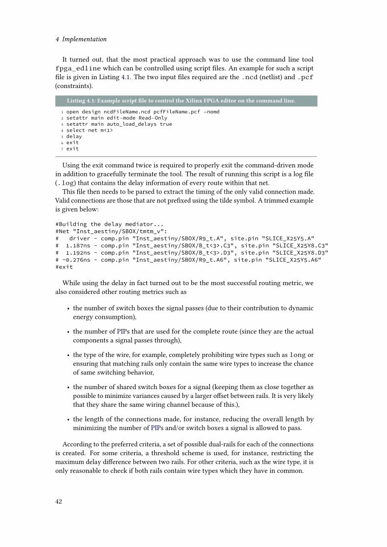
4 Implementation
It turned out, that the most practical approach was to use the command line tool
fpga_edline which can be controlled using script files. An example for such a script
file is given in Listing 4.1. The two input files required are the .ncd (netlist) and .pcf(constraints).
Listing 4.1: Example script file to control the Xilinx FPGA editor on the command line.
1 open design ncdFileName.ncd pcfFileName.pcf −nomd2 setattr main edit−mode Read−Only3 setattr main auto_load_delays true4 select net m<1>5 delay6 exit7 exit
Using the exit command twice is required to properly exit the command-driven mode
in addition to gracefully terminate the tool. The result of running this script is a log file
(.log) that contains the delay information of every route within that net.
This file then needs to be parsed to extract the timing of the only valid connection made.
Valid connections are those that are not prefixed using the tilde symbol. A trimmed example
is given below:
#Building the delay mediator...#Net "Inst_aestiny/SBOX/tmtm_v":# driver - comp.pin "Inst_aestiny/SBOX/R9_t.A", site.pin "SLICE_X25Y5.A"# 1.187ns - comp.pin "Inst_aestiny/SBOX/B_t<3>.C3", site.pin "SLICE_X25Y8.C3"# 1.192ns - comp.pin "Inst_aestiny/SBOX/B_t<3>.D3", site.pin "SLICE_X25Y8.D3"# ~0.276ns - comp.pin "Inst_aestiny/SBOX/R9_t.A6", site.pin "SLICE_X25Y5.A6"#exit
While using the delay in fact turned out to be the most successful routing metric, we
also considered other routing metrics such as
• the number of switch boxes the signal passes (due to their contribution to dynamic
energy consumption),
• the number of PIPs that are used for the complete route (since they are the actual
components a signal passes through),
• the type of the wire, for example, completely prohibiting wire types such as long or
ensuring that matching rails only contain the same wire types to increase the chance
of same switching behavior,
• the number of shared switch boxes for a signal (keeping them as close together as
possible to minimize variances caused by a larger offset between rails. It is very likely
that they share the same wiring channel because of this.),
• the length of the connections made, for instance, reducing the overall length by
minimizing the number of PIPs and/or switch boxes a signal is allowed to pass.
According to the preferred criteria, a set of possible dual-rails for each of the connections
is created. For some criteria, a threshold scheme is used, for instance, restricting the
maximum delay difference between two rails. For other criteria, such as the wire type, it is
only reasonable to check if both rails contain wire types which they have in common.
42

4.2 Customized Router using RapidSmith
Very often, a cascaded approach was used such that if the first criterion did not result in
any routes, a second criterion was used (and so on). This scheme could also be extended to
choose routes from multiple criteria if the number of routes was less than a certain amount.
By applying and considering the various criteria, the set of possible routings can be
shrunk. The final step is then to convert the output into a SAT problem to be able to select
a conflict-free routing. If the encoded problem is satisfiable, the solution is put together
and written to a new XDL file. All the previously routed nets are then locked, while the
remaining unrouted nets are auto-routed by using fpga_edline.
4.2.2 Router Structure
The router and the developed files are contained in the following packages:
• de.emsec.debugdev: This package contains helper functions that were usefulfor the development.
• de.emsec.rs.route: Several new classes to represent routes (see explanation
below and Figure 4.7).
• de.emsec.util: Several helper classes to provide parallelized calls to the Xilinx
tools. The parallelized calls are done using the Java interface Callable.
• edu.byu.ece.rapidSmith.router:
– BasicDualRailFileCreator.java:
– FinalDualRailClauseGenerator.java:
– BasicDualRailRouter.java:
Router Workflow
The router is following a specific workflow to realize the balanced routing. This sequence
is sketched in Figure 4.6 and outlined below:
(1) The whole process starts with providing the appropriate XDL file. This file must be
created from the NCD file created by map.(2) The Java class BasicDualRailFileCreator.java must be used to create serial-
ized timing evaluated routings. Each file being created contains a reasonable large amount
of routing possibilities that have been analyzed for their delay.
(3) The Java class FinalDualRailClauseGenerator.java is used to process the
serialized routing information to create a conditioned set (according to the selected metric).
The resulting set is then converted into a SAT problem and solved using the SAT solver
CryptoMiniSat 2.9.6∗. If the problem can be solved, the result is mapped back to the
original routes which are then copied into the design. This partially design is then written
to the hard disk as an XDL file.
(4) The intermediate XDL file must then be converted back to NCD such that it can be
processed by the Xilinx FPGA editor again. This editor must then be used to lock all
previously routed nets by using a script file that was created beforehand. After locking
all nets, the remaining (and unrouted) nets are then auto-routed. The fully routed file can
then be further processed by bitgen and used as configuration for the FPGA.
∗Available as download here: https://gforge.inria.fr/projects/cryptominisat/
43
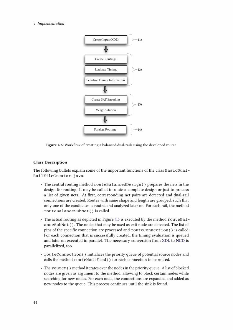
4 Implementation
Create Routings
Evaluate Timing
Serialize Timing Information
Create SAT Encoding
Merge Solution
Create Input (XDL)
Finalize Routing
(1)
(2)
(3)
(4)
Figure 4.6: Workflow of creating a balanced dual-rails using the developed router.
Class Description
The following bullets explain some of the important functions of the class BasicDual-RailFileCreator.java:
• The central routing method routeBalancedDesign() prepares the nets in the
design for routing. It may be called to route a complete design or just to process
a list of given nets. At first, corresponding net pairs are detected and dual-rail
connections are created. Routes with same shape and length are grouped, such that
only one of the candidates is routed and analyzed later on. For each rail, the method
routeBalanceSubNet() is called.
• The actual routing as depicted in Figure 4.5 is executed by the method routeBal-anceSubNet(). The nodes that may be used as exit node are detected. The list of
pins of the specific connection are processed and routeConnection() is called.
For each connection that is successfully created, the timing evaluation is queued
and later on executed in parallel. The necessary conversion from XDL to NCD is
parallelized, too.
• routeConnection() initializes the priority queue of potential source nodes and
calls the method routeModified() for each connection to be routed.
• The routeM()method iterates over the nodes in the priority queue. A list of blocked
nodes are given as argument to the method, allowing to block certain nodes while
searching for new nodes. For each node, the connections are expanded and added as
new nodes to the queue. This process continues until the sink is found.
44

4.2 Customized Router using RapidSmith
To implement the desired functionality, it was helpful to increase the number of classes
and objects to achieve a more descriptive code. One example for this is how net lists are
represented. Beforehand, a net list (a list which holds all PIPs) was implemented as:
ArrayList<PIP> someNetList;
While this is sufficient to be put into a complete design, it is not suited to represent single
and dual-rail signals at the same time. In addition to that, it cannot be used to represent
different connections and routing candidates within the same net (or pair of nets). To
overcome these limitations, new classes were introduced. The structure is based on the two
classes DualRailRoute and SingleRailRoute that both inherit the abstract parent
class SignalRoute. By using this object oriented approach, checking routes for their
possible conflicts is simple.
Furthermore, dual-rail and single-rail routes can be represented using a single variable
within the SAT encoding. This enables us to route some single-rail signals as well, for
example, some designs may fail to be auto-routed by fpga_edline after doing the
balanced routing. If this happens, one can manually include critical single-rail signals to
the customized router, thereby considering these additional conflicts in the SAT encoding.
This step is sometimes required to route one of the enable signals on the output stage of
the S-box.
+ causesConflict abstract
- netName : String- ps : Integer- hops : Integer
SignalRoute abstract
Comparable Serializable
+ causesConflict
- delta : Integer- deltaHops : Integer- rail_t : SingleRailRoute- rail_v : SingleRailRoute
DualRailRoute
+ causesConflict- rail : ArrayList<<PIP>>
SingleRailRoute
Figure 4.7: UML class diagram showing the two basic data types used to represent signal
routes.
Finding Similar Routes – Serializing Timing
As stated before, it is necessary to find similar routes and only evaluated one candidate of
this set for its timing. Otherwise, the overall process would be too slow. To find similar
45
4 Implementation
routes, the x and y offset of the source and sink pin must be the same with the other route.
However, this could possibly lead to situations when one slice with odd x coordinate has
the same offset with another route that starts in a slice with an even x coordinate. This
would cause problems because routes from the “upper” slice of a switch box cannot be
copied to any of the outputs of the “lower” slice.
To solve this, we simply add a z coordinate which is defined as: z = x mod 2. In addition
to that, further information is required to properly address gates in the LUTs, for instance,
if a gate occupies the lower two or upper two LUTs of a slice.
For each of the candidates, a unique string is then used to write the serialized result to the
hard disk. The SAT encoder can then read back the results and create the set accordingly
to the metric selected.
4.2.3 Implementation Considerations
While first facing the given problem, the solution was not clear-cut. In addition to that,
there is no comparison with other references possible since there is no other publication
that would address the described problems in the same way. It is therefore even more
important to reason about the techniques used to implement the router and justify for the
decisions made.
Copy-Paste Approach
It is evident that even for small designs, the time required to evaluate the timing of the
routes becomes a critical issue. For the case of AWDDL logic, a total of 122 AWDDL gates
and 8 additional LUTs for the single-to-dual-rail conversion exist. This results in a total
number of 606 dual-rail connections.
The step that extracts the possible routes and timing requires around 6 hours, though
being massively parallelized using 16 cores (siblings). Compared to that does the SAT
solving and encoding take less than 20 minutes. The actual execution time depends on the
metric chosen and the size of the set that must be processed.
These numbers are for the case that a copy-paste approach is used. While this induces
a certain uncertainty about the actual timing (see Section 4.4), it is clear that not using
a copy-paste approach would result in a dramatically increased runtime, especially for
designs that might use masking in addition to a customized logic style. So, unless there is a
better way to obtain the timing, we consider this as the only practical approach, at least for
the feedback loops in the design.
Resolving Conflicts
There are different approaches to tackle routing conflicts. The first decision must be made
between “static” and “dynamic” conflict detection.
• Static conflict detection is the setting when all possible routes are known prior routingsuch that if a conflict occurs, a new route from the given set can be selected. This
approach has the advantage that all available routes can be found at the cost of time
and memory. From that point on, it could be theoretically possible to also find the
optimum solution.
46
4.2 Customized Router using RapidSmith
• Dynamic conflict detection takes place under the assumption that the router is
instantaneously started on some route (possibly using a heuristic, e.g., starting with
the most critical routes). For each route that is created, the used resources are marked
as being occupied.
Now, two options exist while routing the next route: Either react to the occupied
resource by avoiding its use, or overusing the particular resource regardless of the
fact that it is used by another route. This step would then result in an iterative
approach and multiple runs, each time trying to reduce the number of resource
conflicts, whereas the other approach might get stuck if no more resources can be
selected.
For this thesis, the static approach appeared to be the most promising one, since there
was no prior knowledge about the internal FPGA architecture and it was not known, if
finding balanced routes is possible at all. The size of the problem still allows to exhaustively
create all routes and then select a conflict free set. In addition to that, it is in the interest
from a security point of view to get the best possible routing (almost) regardless of the
running time to create it. In conjunction with the previous two choices, one can distinguish
between various methods on how to obtain such a conflict free routing:
• Greedy: By using a greedy approach which is selecting routes on a “first one fits”
approach, one can get stuck easily in local minima or unsolvable situations. By
practically exploring this method, we found out that for most cases it is indeed
impossible to find a solution using the greedy algorithm.
• Simulated Annealing mimics the behavior of cooling molecules that form crystal
structures. It can be used for both placement and routing. Initially, the elements are
in a state that accepts moves requiring a high cost and that may even make the overall
result worse. This is the state when the temperature is high. With each movement,
the temperature cools down and the elements may only do smaller movements. By
doing so, local minima and maxima can be avoided. The movement of the elements
requires a certain heuristic and may be slow for use cases with many elements [McM].
For routing, one can expect that CSP or SAT are likely to yield better results in shorter
time.
• CSPs: Solvers for CSPs are used for mathematical problems that can be encoded using
a set of objects whose state must be satisfied by the given constraints. The concepts
of solving CSPs and SAT are different but dual to each other. Various research articles
analyze how one can map a CSP to SAT and vice-versa [Wal12].
Unlike SAT, it should be possible to assign costs to the objects being selected, thus
making it possible to reduce the overall cost (e.g., the overall difference of all selected
dual-rails). Compared to the SAT solution, this appears to be more complex and was
not as accessible to the author. This idea may be part of additional research.
• Iterative Repair: Iterative repair methods route once and then check if resources have
been overused. If such resources exist, the affected routes get rerouted. Based on the
observation how the ISE tools work, we assume that Xilinx uses such an approach.
This not only requires a reasonable good starting point but also a heuristic which
decides on which routes to ripup. These heuristics require extensive knowledge about
the routing architecture and require to estimate the routing channel consumption.
47

4 Implementation
• Customized Backtrack: All CSP solvers as well as SAT solvers rely on some sort
of backtracking. In the beginning of this thesis, a small attempt has been made in
implementing a customized backtracking solution especially tailored for the given use
case. While this solution was working, it completely lacked the advanced features of
both CSP and SAT solvers, such as forward checking or conflict-directed backjumping
[Pro93]. This lack of functionality makes a simple backtracking approach too slow
to be applied to a real-world problem.
4.3 FPGA Approach to Secure Logic
As part of this thesis, an existing AES design was made available to the author. This AES
design is originally based on David Canright’s S-box [Can05], whereas the actual logic was
realized by 2-input Level-Encoded Dual-Rail Logic (LEDR) gates. These are implemented
using manually instantiated LUTs [Xil12b].
By making the attempt to route the design, it was found out that the implemented logic
was trimmed due to “optimizations” carried out by Xilinx ISE. It was therefore necessary to
delve into the various Xilinx constraints to improve the existing design and make a proper
AWDDL design later on.
Beforehand, custom logic gates (e.g., LEDR) were split and scattered around. Moreover,
logic was placed into slices that contained other logic, possibly causing undesired side-
effects. To solve these issues, the following constraints were used [Xil12c]:
• The “Save Net Flag” is a basic mapping constraint. It prevents the removal of loadless
or driverless signals and may also prevent trimming of logic which is connected to
the signal.
• The “No Reduce” constraint is a synthesis constraint which prevents the minimization
of redundant logic. When creating combinatorial feedback latches in a design, the No
Reduce constraint must be applied to the latch output net. According to the Xilinx
Constraints Guide [Xil12c], it is not applicable to FPGAs but works anyway.
• The “Keep” constraint is an advanced mapping and synthesis constraint. It causes
affected signals to be kept during both synthesis and implementation if the option
true is used.
• The “Hierarchical Block Name” (HBLKNM) is an advanced mapping constraint that
assigns block names to logic elements based on the level in the hierarchy. It forces
function generators and flip-flops to be in the same CLB. Adding the hierarchy name
to the actual block name is required since each logic gate is instantiated multiple
times.
• The “BEL” constraint is an advanced mapping constraint that locks a logical symbol
to a particular component, for example, to one of the specific LUTs (A, B, C, or D).
To ensure the same placement for all of the designs, the S-box was first placed using a
closed group which is area constrained. Afterwards, the specific gates were locked to these
assigned locations (using LOC constraints). When updating the design to a new logic style
(e.g., from LEDR to AWDDL), the placement was kept the same.
The resulting module for an AWDDL XOR gate is shown in Listing 4.2. This example
places the LUTs in the fixed positions A and B.
48

4.3 FPGA Approach to Secure Logic
Listing 4.2: AWDDL gate implementing an Exclusive OR (XOR).
1 module xor_awddl(v1, t1, v2, t2, v3, t3);2 (* S="TRUE" *) input t1;3 (* S="TRUE" *) input t2;4 (* S="TRUE" *) input v1;5 (* S="TRUE" *) input v2;6 (* S="TRUE" *) output t3;7 (* S="TRUE" *) output v3;8
9 wire t3_DUMMY;10 wire v3_DUMMY;11
12 assign v3_DUMMY = v3;13 assign t3_DUMMY = t3;14
15 (* LOCK_PINS="ALL" *)16 (* BEL="A6LUT" *)17 (* HBLKNM="XORPACK" *)18 (* NOREDUCE="TRUE" *)19 (* KEEP="TRUE" *)20 LUT6 #( .INIT(64’hfffefffeeac0eac0) ) TruePart (21 .I0(v1),22 .I1(t1),23 .I2(v2),24 .I3(t2),25 .I4(1’b0),26 .I5(v3_DUMMY),27 .O(v3));28
29 (* LOCK_PINS="ALL" *)30 (* BEL="B6LUT" *)31 (* HBLKNM="XORPACK" *)32 (* NOREDUCE="TRUE" *)33 (* KEEP="TRUE" *)34 LUT6 #( .INIT(64’hfffefffeeca0eca0) ) FalsePart (35 .I0(v1),36 .I1(t1),37 .I2(v2),38 .I3(t2),39 .I4(1’b0),40 .I5(t3_DUMMY),41 .O(t3));42
43 endmodule
A slice of a Virtex-5 is able to hold 4 LUTs in total. Several attempts have therefore been
made to do a pairwise placement of gates in a slice, such that a gate with its two LUTs is
either placed in (A,B) or (C,D). According to the author’s experience this does not appear
to be possible by using the available tools. The best attempt that could be made was using
the following constraints:
• Instead of the “BEL” constraint, an RLOC constraint with 0 as the x and y coordinate
was used, effectively causing the module to be placed into the same slice (however,
this does not guarantee that the placement is always in (A,B) or (C,D)).
• The HBLKNM constraint groups instances (here, two LUTs) together which is im-
portant for keeping them in a single slice. At the same time however, it prevents
packing with other logic because of the different hierarchy level. Just assigning a
Block Name (BLKNM) is not possible because the module is instantiated multiple
times. To solve this issue, a “Hierarchical User Set” can be defined. This constraint
is an advanced mapping constraint that explicitly creates a hierarchically qualified
49

4 Implementation
name for the set. This makes it possible to place two HBLKNM constraint modules
into the same slice.
While this approach should be working, it fails if all affected modules (e.g., XOR, NAND,
NOR, XNOR) are constrained in the described way. If only one of the gate types is excluded
(e.g., NAND), then the placement succeeds (of course, the excluded gate type is then not
placed in the way intended). This situation could not be resolved even when setting
XIL_PAR_ENABLE_LEGALIZER to 1, which uses an alternate algorithm for placement with a
longer run time. This approach is documented in Listing 4.3.
Listing 4.3: Alternative approach using different constraints
1 module xor_awddl(v1, t1, v2, t2, v3, t3);2 // ...3
4 (* LOCK_PINS="ALL" *)5 (* RLOC = "X0Y0" *)6 (* HU_SET = "AWDDL" *)7 (* HBLKNM="XORPACK" *)8 (* NOREDUCE="TRUE" *)9 (* KEEP="TRUE" *)10
11 // ...12 endmodule
4.4 Determining FPGA Settings
At the very beginning of this research the FPGA was analyzed to find out about reasonable
constraints and thresholds for conditioning the obtained set of routes. Concerning the
delay, the first thing to notice is that if a signal splits right before a LUT and connects to
two of its input pins, then there will be a minor delay difference for these two input signals.
Depending on the exact input configuration of that LUT, the difference is always very
small, usually smaller than 10 ps. Of course, this may still be enough to cause an imbalance
that can be exploited by a Side Channel Analysis.
Related to the paper [He+12], one might assume that using routes of the same shape
and length is the best possible case of achieving symmetry and balance between two rails.
This must not necessarily be true in an FPGA. Various configurations indicate that there is
always a minor (but possibly significant) deviation of the signal delay. Therefore, copying
the route and using it in a different area may result in a different timing. To exhibit this
behavior, a well balanced dual-rail was chosen and copied to different areas of the FPGA as
it is shown in Figure 4.8. The chosen route itself was already illustrated in Figure 3.8 with
its corresponding XDL representation next to it.
With the help of Table 4.1, one can recognize that even in this best-case, the delay
difference |∆d | is different. However, comparing our use case and the one presented in
the paper from ReConfig’12 [He+12], a difference is striking. In their case, one would
copy routes only from the first (or second column) from Table 4.1 and use these copies as
dual-rails, for instance, entry #1 and entry #9 from the first column, resulting in a difference
of 11 ps. For other situations, for instance, when passing the switch box of either a BRAM
or DSP (entries #11 and #12), the delay difference may differ even worse.
For situations when we copy single rails and match themwith other rails, we also observe
a larger difference between two dual-rails. Therefore, evaluating the timing of each possible
50

4.4 Determining FPGA Settings
route would be indeed the best solution but due to the time required to do so it is not
feasible for practical use.
In case of a default routing it can be observed that the delay difference between two rails
is approximately 60 ps in the best case. Taking the previous findings into consideration,
it makes sense to aim for a delay difference which is less than 60 ps, whereas an average
delay difference below 10 ps becomes unlikely, simply due to the described situation for
two input pins of the same LUT.
1234
5
67
8
10
9
12
11
Figure 4.8: Overview of the same connection that was evaluated with a different offset.
51

4 Implementation
Table 4.1: Overview of the evaluated timings as shown in FIgure 4.8. All values are in
picoseconds.
# d (m< 1 >) d (m< 0 >) |∆d | Slice Source Slice Sink
1 1018 1018 0 X1Y0 X7Y02 1015 1013 2 X1Y1 X7Y13 1011 1013 2 X1Y2 X7Y24 1011 1013 2 X1Y3 X7Y35 1011 1009 2 X13Y1 X19Y16 1007 1009 2 X13Y3 X13Y37 1011 1013 2 X15Y4 X15Y48 1011 1009 2 X21Y9 X21Y99 1007 1009 2 X21Y19 X27Y1910 1013 1017 4 X1Y10 X7Y10
11 1030 1032 2 X9Y7 X13Y7
12 1097 1100 3 X5Y5 X9Y5
52
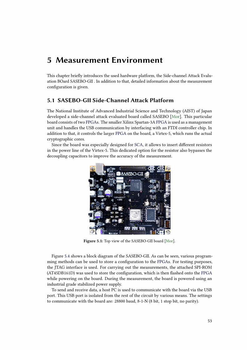
5 Measurement Environment
This chapter briefly introduces the used hardware platform, the Side-channel Attack Evalu-
ation BOard SASEBO-GII . In addition to that, detailed information about the measurement
configuration is given.
5.1 SASEBO-GII Side-Channel Attack Platform
The National Institute of Advanced Industrial Science and Technology (AIST) of Japan
developed a side-channel attack evaluated board called SASEBO [Mor]. This particular
board consists of two FPGAs. The smaller Xilinx Spartan-3A FPGA is used as a management
unit and handles the USB communication by interfacing with an FTDI controller chip. In
addition to that, it controls the larger FPGA on the board, a Virtex-5, which runs the actual
cryptographic cores.
Since the board was especially designed for SCA, it allows to insert different resistors
in the power line of the Virtex-5. This dedicated option for the resistor also bypasses the
decoupling capacitors to improve the accuracy of the measurement.
Figure 5.1: Top view of the SASEBO-GII board [Mor].
Figure 5.4 shows a block diagram of the SASEBO-GII. As can be seen, various program-
ming methods can be used to store a configuration to the FPGAs. For testing purposes,
the JTAG interface is used. For carrying out the measurements, the attached SPI-ROM
(AT45DB161D) was used to store the configuration, which is then flashed onto the FPGA
while powering on the board. During the measurement, the board is powered using an
industrial grade stabilized power supply.
To send and receive data, a host PC is used to communicate with the board via the USB
port. This USB port is isolated from the rest of the circuit by various means. The settings
to communicate with the board are: 28800 baud, 8-1-N (8 bit, 1 stop bit, no parity).
53

5 Measurement Environment
To send bytes, the following command must be used (see Figure 5.2):
0 1 2 3 4 5 6 7 8 9 10 11 12 13 14 15 16 17 18
FF HI LO 16 Bytes Plaintext
Figure 5.2: Command to send plaintext bytes to the cryptographic unit. HI and LO may be
used as a counter for the number of iterations to be performed.
To reset the cryptographic circuit, the following command is used (see Figure 5.3):
0 1 2 3 4 5 6 7 8 9 10 11 12 13 14 15 16 17 18
FF 00 01 FF. . . FF 00
Figure 5.3: Command to reset the cryptographic unit.
Figure 5.4: Block diagram of the SASEBO-GII board [Mor].
5.2 Oscilloscope / Settings
The power traces are measured using a LeCroy HRO 66Zi oscilloscope. It is a 600 MHz
Digital Sampling Oscilloscope (DSO), with 4 scope channels and an analog/digital resolution
of 12-bit. The oscilloscope is capable of a maximum sample frequency of 2 GS/s. For the
measurements however, a sample frequency of 1 GS/s is used, while the design runs at a
clock frequency of 3 MHz.
To reduce the length of each measurement, a trigger signal is used to indicate when the
cryptographic operation starts. The time window is set to 1 ms.
54

6 Practical Results
In this section, we give practical results for the most promising result only, since a huge
variety of possible routings has been created. Among the many routings that have been
created, we observed routings that performed equally, better, or sometimes even worse
than the default routing.
Due to limited hardware resources and authorization, the measurements and security
evaluations have been carried out by my supervisor, Amir Moradi. This joint work resulted
in a paper submission to the conference “Design, Automation & Test in Europe” 2014 (Date).
The author of this thesis would therefore like to acknowledge this joint work and point out
that Figure 6.3 was created as part of the security evaluation which is also contained in the
submitted paper.
6.1 Obtained Routings
The various routings were analyzed accordingly to the metrics chosen. In case of the delay,
routings have been analyzed with an average delay difference of 11.69 ps up to 125.27 ps.
We also analyzed how many connections are of the same wire type, ranging from all
connections to almost none. It should be noted that analyzing designs just by one metric is
not possible. An example to prove this is in case wires are forced to pass the same switch
box. Due to the architecture of the FPGA this automatically decreases the amount of routes
with very low delay difference. Other metrics are also working in opposite directions.
For a fair comparison of the designs, we only modified the contents of the LUTs to change
from one logic style to another. The placement was kept the same. With this approach, we
evaluated three design profiles:
1. WDDL AES S-box routed by ISE,
2. AWDDL AES S-box, the same routing as profile 1,
3. AWDDL AES S-box routed by our customized router.
Accordingly to ISE, the maximum frequency of profile 2 and 3 were similar (33.722 MHz
and 30.089 MHz). However, these numbers should be treated with utmost care because of
the lack of support for asynchronous circuits. The analyzed path was indeed not correct.
The analyzed architecture consists of the input encoding to convert from a single-rail to
a dual-rail style, followed by the actual S-box and the output stage. It is worth mentioning
that the output registers were put in the slice of the last AWDDL gate. This architecture is
sketched in Figure 6.1. The path analyzed by ISE was starting from the output register of
the enable signal eno through the “to WDDL” conversion stage and the S-box. Clearly,
this is not the path the signal takes.
55

6 Practical Results
Control Logic
toWDDL
SboxWDDL/AWDDL
FF
FF
FF
in
eni eno
out
pr
Figure 6.1: Block diagram of the analyzed S-boxmodule.
To compare the result of default and customized routing, two histograms have been
created that can be seen Figure 6.2. The histogram uses bins of 10 ps and considers the
difference between the delay of each dual-rail signal in the S-box circuit. Even though it is
not possible to find dual-rail routes with zero delay difference in each case, the histograms
still indicate the effectiveness of the approach taken.
To emphasize this, it should be mentioned that the average delay difference of the
customized routing was 11.69 ps compared to 125.27 ps of the default routing. The worst
imbalance in the customized routing was just 58 ps compared to 520 ps of the default
routing.
050100150200250300350
0 50 100 150 200 250 > 300
No.
ofoc
curenc
es
Delay Difference [ps]
our customized routerISE router
Figure 6.2: Histogram of the delay difference of all dual-rail routes
6.2 Practical Investigations
The fair evaluation of the different implementations was done using the information
theoretic metric of [SMY09] which allows quantify the leaked information without making
assumptions about the leakage model. This metric has been applied on mean traces
obtained from 2000 traces for each possible S-box input byte value. Therefore, a total
of 2000 · 256 = 512, 000 traces have been collected for each design.
This analysis leads to the mutual information curves as shown in Figure 6.3. The
comparison of Figure 6.3a and Figure 6.3b shows that the information leakage is significantly
reduced by the self-timed approach of AWDDL. This proves that the early-propagation
indeed affects the security in a practical design.
Furthermore, by applying our customized router on the AWDDL design, it can be shown
that the information leakage can be reduced even more. Still, the implementation shows a
certain leakage.
56

6.2 Practical Investigations
0.4
MutualInfo.
Time [ns]0
0250 500 750 1000
(a) Profile 1
0.4
MutualInfo.
Time [ns]0
0250 500 750 1000
(b) Profile 2
0.4
MutualInfo.
Time [ns]0
0250 500 750 1000
(c) Profile 3
8
6
4
2MutualInfo.
log(noise standard deviation)−4 −3 −2 −1
00
Prole 1Prole 2Prole 3
(d) Over the noise
Figure 6.3: Mutual information curves for all three profiles.
57

6 Practical Results
6.3 Implications
By applying various metrics to create different routings, we could compare the impact of the
routing on the extractable leakages. Contrary to the original expectations were the metrics
related to the number of switch boxes and/or PIPs less important than the delay difference.
One possible explanation is that by minimizing the delay difference, some architectural
properties of the FPGA are implicitly considered as well. If doing a default routing, it can
be observed that obtaining dual-rail routes with a difference smaller than 60 ps becomes
very unlikely (see also Section 4.4) which is exactly the opposite of the chosen metric which
led to the best result.
Moreover, by selecting the same feedback loops at every LUT, the remaining choices
for doing the routing is decreased. This increases the likelihood of creating more similar
routes for any other connection.
Another explanation may be derived from the situation when a net has one source
pin and multiple sink pins. In the very beginning of this thesis it was observed that the
extracted delay from a single connection did not change if more connections of the same
net get actually routed and thus connected to the same source pin (driver).
If one would start adding more capacitors to that net (as equivalents for gates) the single
driver would need to drive more capacitance – therefore slowing down the signal seen by
the gates connected to that source. This does not appear to be the case for the nets with
rather small fanout that were considered as part of the S-box.
This idea can be transferred to the case of two dual-rails. Clearly, the capacitance
imbalance causes the delay of the rails to be different. Then, the arrival time of a dual-rail
input signal of a gate depends on its value. Combinational circuits made from AWDDL
gates without early propagation fire their output when all input signals arrived, however,
the time of evaluation of the gate will still depend on its input values. This may still
propagate through the whole circuit possibly making the power consumption pattern
different depending on the circuit input value.
Though the exact cause of the increased security could not be fully determined without
further research and the lack of documentation, it was shown that the security can be
increased at no cost simply by optimizing the routing. This result may hopefully inspire
the FPGA manufacturers to take into account new metrics in their tools to consider the
sensitive routing requirements of cryptographic circuits.
58

7 Conclusion
The following section summarizes the work that has been carried out. In addition to that,
possible ideas for future work are presented.
7.1 Summary
The objective of this work is to improve the security in FPGAs by implementing secure logic
styles that help minimizing the leakage in a cryptographic device. Such logic styles use dual-
rail logic to equalize the power consumption, thereby minimizing the leakage. However,
this only works if each signal pair is balanced. The question that is being addressed in this
thesis is how this balance between two rails can be increased and also by which metric the
best result can be achieved. None of the available vendor tools would allow such a deep
control over the routing process in an FPGA.
This thesis therefore presents a router that contains the tools necessary to implement a
design that requires balanced routing. The router was implemented with the least possible
impact on the overall tool flow and could also be used to create hard macro instances of
balanced logic. The suitability for practical use has been proven by implementing two
asynchronous dual-rail logic styles.
An important conclusion that can be drawn based upon the evaluation is that finding a
reliable metric is difficult. This is owed to the fact that only scarce information about the
routing architecture in FPGAs is known. Using the router still requires a deep understanding
of the underlying architecture and more knowledge provided by Xilinx would be helpful.
Using the developed router is strongly recommended for small designs, since the XDL to
NCD conversion adds the most overhead and is responsible for the majority of the toolkit’s
execution runtime. The router presented in this thesis is therefore by no means a complete
replacement to the existing Xilinx workflow; however, it should be used as an auxiliary
router along with the Xilinx tools if required.
In addition, debugging issues are mostly related to the SAT solver which is treated as a
black box. It is never known which routes prohibit a successful routing and the only way
to circumvent this is to adjust the threshold for the routing selection. This can only be
done by trial and error and a more analytical approach would be desirable.
In spite of these limitations, it was proven that the developed router is able to significantly
reduce the leaked information by routing well-balanced dual-rails. Moreover, by storing
the timing information after they have been obtained once, it is possible to create multiple
routings much faster.
7.2 Future Work
This master’s thesis has been carried out in limited time. Hence, there is scope for future
work. We therefore present several ideas to improve and extend this thesis. The first set of
ideas addresses the developed tool:
59

7 Conclusion
Timing Extraction: Since the timing extraction imposes the largest overhead, a new
method needs to be developed to obtain the delay of the signals. The easiest possible
solution would be an API provided by Xilinx. However, this does not appear to be a
promising solution at the moment. Therefore, a theoretic model must be derived that allows
to calculate the delays without any use of the Xilinx tools.
Measuring Delay: The validity of the approach used relies on the conformity of the
reported delay numbers with the actual FPGA. It is therefore important to verify that these
numbers are in fact a valid source of information that allow to balance dual-rail signals.
Hence, each rail must be measured and compared to the reported number. In addition to
that, one must investigate how process variation might effect the findings.
Simulated Annealing or CSP: Our approach relies on a SAT solver which makes the
optimization towards a certain metric difficult. Unsatisfiable routings are also difficult to
debug, as there is no information as to why it is unsatisfiable. Simulated annealing or a CSP
solver could help to target the first issue, as it allows to optimize the data until a certain
confidence level is reached.
In addition to that, the following two ideas appear interesting:
Masked Version: As part of this thesis, only non-masked versions have been analyzed.
It is a well-known issue that by using a single countermeasure, it is not possible to eliminate
the leakage. Therefore, different countermeasures should be combined, such as masking and
a secure logic style, to reach a level of security that is interesting for real-world applications.
This has been part of the submitted paper.
Degradation of Routes: The security of the approach relies on the balance between
both rails. The question is: Is it possible to deliberately degrade rails of a signals (by aging)
such that one can induce a larger imbalance between both rails that can ultimately be
exploited to mount an attack?
60
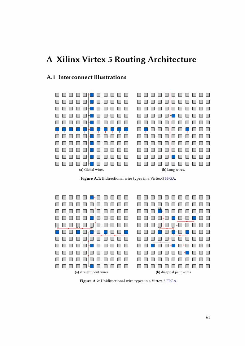
A Xilinx Virtex 5 Routing Architecture
A.1 Interconnect Illustrations
(a) Global wires. (b) Long wires.
Figure A.1: Bidirectional wire types in a Virtex-5 FPGA.
BEGMIDEND
(a) straight pent wires
BEGMID
END
(b) diagonal pent wires
Figure A.2: Unidirectional wire types in a Virtex-5 FPGA.
61

A Xilinx Virtex 5 Routing Architecture
BEGMIDEND
(a) straight double wires
BEGMID
END
(b) diagonal double wires
Figure A.3: Unidirectional wire types in a Virtex-5 FPGA.
62
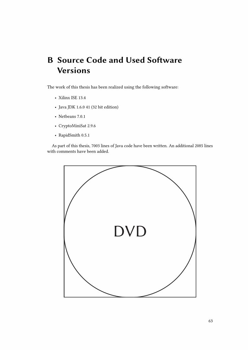
B Source Code and Used Software
Versions
The work of this thesis has been realized using the following software:
• Xilinx ISE 13.4
• Java JDK 1.6.0 41 (32 bit edition)
• Netbeans 7.0.1
• CryptoMiniSat 2.9.6
• RapidSmith 0.5.1
As part of this thesis, 7003 lines of Java code have been written. An additional 2085 lines
with comments have been added.
DVD
63


List of Figures
3.1 Figure illustrating the naming scheme within an FPGA. Both slice and RPM
coordinates (in gray) are shown. . . . . . . . . . . . . . . . . . . . . . . . . 16
3.2 A simplified diagram of a Xilinx Virtex-5 slice. . . . . . . . . . . . . . . . . 17
3.3 A possible realization of a PIP that is controlled by an SRAM cell. Based
on [Wol04]. . . . . . . . . . . . . . . . . . . . . . . . . . . . . . . . . . . . . 18
3.4 Wire distance metrics. Based on [Wol04]. . . . . . . . . . . . . . . . . . . . 19
3.5 Virtex-5 Interconnection Architecture according to [Xil06]. . . . . . . . . . 21
3.6 This screenshot taken from the Xilinx FPGA editor shows two tiles eachwith
their corresponding switch box and pair of slices. The numbers assigned
are: 1 pent wires 2 double wires 3 bounceacross wires 4 horizontal
long wires 5 global wires 6 vertical long wires 7 global switch box 8
local switch box 9 slices . . . . . . . . . . . . . . . . . . . . . . . . . . . . 23
3.7 Example illustrating almost all possible interconnects within an FPGA
switch box. Each line is representing a possible interconnect. Using the
Xilinx FPGA editor, yellow and purple lines are used to distinguish between
incoming and outgoing connections. Clearly visible are the bounce wiresthat get redirected. . . . . . . . . . . . . . . . . . . . . . . . . . . . . . . . 24
3.8 Example of a well-balanced dual-rail signal from one slice to another. . . . 29
3.9 Illustration of a CMOS inverter. . . . . . . . . . . . . . . . . . . . . . . . . 31
3.10 Illustration of WDDL gates including precharge generation [TV04]. . . . . 32
3.11 Comparison of a single-rail and WDDL NAND element in terms of static
and dynamic power consumption. Based on [Sin11] . . . . . . . . . . . . . 33
3.12 AWDDL AND/NAND gate∗[MI]. . . . . . . . . . . . . . . . . . . . . . . . . 34
4.1 The design flow using RapidSmith in conjunction with Xilinx tools. . . . . 37
4.2 The major classes in RapidSmith used to represent a design. Based on:
[Lav+12] . . . . . . . . . . . . . . . . . . . . . . . . . . . . . . . . . . . . . 38
4.3 The major classes in RapidSmith used to represent a device. Based on:
[Lav+12] . . . . . . . . . . . . . . . . . . . . . . . . . . . . . . . . . . . . . 39
4.4 This figure illustrates the customized workflow used in this thesis. . . . . . 40
4.5 Basic idea how to create multiple routing candidates . . . . . . . . . . . . . 41
4.6 Workflow of creating a balanced dual-rails using the developed router. . . 44
4.7 UML class diagram showing the two basic data types used to represent
signal routes. . . . . . . . . . . . . . . . . . . . . . . . . . . . . . . . . . . . 45
4.8 Overview of the same connection that was evaluated with a different offset. 51
5.1 Top view of the SASEBO-GII board [Mor]. . . . . . . . . . . . . . . . . . . 53
5.2 Command to send plaintext bytes to the cryptographic unit. HI and LOmay be used as a counter for the number of iterations to be performed. . . 54
5.3 Command to reset the cryptographic unit. . . . . . . . . . . . . . . . . . . 54
65
List of Figures
5.4 Block diagram of the SASEBO-GII board [Mor]. . . . . . . . . . . . . . . . 54
6.1 Block diagram of the analyzed S-boxmodule. . . . . . . . . . . . . . . . . . 56
6.2 Histogram of the delay difference of all dual-rail routes . . . . . . . . . . . 56
6.3 Mutual information curves for all three profiles. . . . . . . . . . . . . . . . 57
A.1 Bidirectional wire types in a Virtex-5 FPGA. . . . . . . . . . . . . . . . . . 61
A.2 Unidirectional wire types in a Virtex-5 FPGA. . . . . . . . . . . . . . . . . 61
A.3 Unidirectional wire types in a Virtex-5 FPGA. . . . . . . . . . . . . . . . . 62
66

List of Tables
2.1 Truth table for the Boolean implication A⇒ B. . . . . . . . . . . . . . . . . 7
2.2 Truth table for the boolean expression ¬A ∨ ¬B used to encode selection
conflicts. . . . . . . . . . . . . . . . . . . . . . . . . . . . . . . . . . . . . . 7
3.1 Comparison between the routing resources of Virtex-4 and Virtex-5 [MK09]. 21
3.2 Small computation to explain how DIRTs work. This example is for one of
the two sink pins of a net. . . . . . . . . . . . . . . . . . . . . . . . . . . . . 26
3.3 Small computation to explain how DIRTs work. This example is for one of
the two sink pins of a net. . . . . . . . . . . . . . . . . . . . . . . . . . . . . 26
4.1 Overview of the evaluated timings as shown in FIgure 4.8. All values are in
picoseconds. . . . . . . . . . . . . . . . . . . . . . . . . . . . . . . . . . . . 52
67


List of Algorithms
3.1.1 Lee Algorithm [Lee61], algorithm description from [Wik13] . . . . . . . . 20
69

Listings
2.1 Example Dimacs file to solve the 2 × 2 polyomino. . . . . . . . . . . . . . . 10
4.1 Example script file to control the Xilinx FPGA editor on the command line. 42
4.2 AWDDL gate implementing an XOR. . . . . . . . . . . . . . . . . . . . . . 49
4.3 Alternative approach using different constraints . . . . . . . . . . . . . . . 50
71

Bibliography
Books
[GJ90] Michael R. Garey and David S. Johnson. Computers and Intractability; A Guideto the Theory of NP-Completeness. New York, NY, USA: W. H. Freeman & Co.,
1990. isbn: 0716710455.
[LM00] Richard J. Larsen and Morris L. Marx. An Introduction to Mathematical Statis-tics and Its Applications (3rd Edition). 3rd. Prentice Hall, Jan. 15, 2000. isbn:
0139223037.
[CT91] Thomas M. Cover and Joy A. Thomas. Elements of information theory. NewYork, NY, USA: Wiley-Interscience, 1991. isbn: 0-471-06259-6.
[HSH09] P.A. Hsiung, M.D. Santambrogio, and C.H. Huang. Reconfigurable System Designand Verification. Taylor & Francis, 2009. isbn: 1420062662.
[Wol04] Wayne Wolf. FPGA-Based System Design. Prentice Hall, 2004. isbn: 0131424610.
[MC79] C. Mead and L. Conway. Introduction to VLSI Systems. Addison-Wesley, Dec.
1979. isbn: 0201043580.
Articles and Papers
[Eis+08] Thomas Eisenbarth et al. “Physical Cryptanalysis of KeeLoq Code Hopping
Applications.” In: IACR Cryptology ePrint Archive 2008 (2008), p. 58.
[YS07] Pengyuan Yu and Patrick Schaumont. “Secure FPGA circuits using controlled
placement and routing.” In: Proceedings of the 5th IEEE/ACM internationalconference on Hardware/software codesign and system synthesis. CODES+ISSS’07. Salzburg, Austria: ACM, 2007, pp. 45–50. isbn: 978-1-59593-824-4.
[KKT06] Konrad J. Kulikowski, Mark G. Karpovsky, and Er Taubin. “Power attacks on se-
cure hardware based on early propagation of data.” In: In 12th IEEE InternationalOn-Line Testing Symposium. 2006, pp. 10–12.
[He+12] Wei He et al. “Automatic generation of identical routing pairs for FPGA imple-
mented DPL logic.” In: ReConFig. IEEE, 2012, pp. 1–6. isbn: 978-1-4673-2919-4.
[GB65] Solomon W. Golomb and Leonard D. Baumert. “Backtrack Programming.” In: J.ACM 12.4 (Oct. 1965), pp. 516–524. issn: 0004-5411.
[KK07] Will Klieber and Gihwon Kwon. “Efficient CNF Encoding for Selecting 1 from
N Objects.” In: The 4th Workshop on Constraints in Formal Verification (CFV).2007.
[FG10] Alan M. Frisch and Paul A. Giannaros. “SAT Encodings of the AT-Most-k
Constraint.” In: The 9th International Workshop on Constraint Modelling andReformulation (ModRef). 2010.
73

Bibliography
[Knu00] Donald E. Knuth. “Dancing Links.” In: arXiv (2000).
[Bat+11] Lejla Batina et al. “Mutual Information Analysis: a Comprehensive Study.” In:
J. Cryptology 24.2 (2011), pp. 269–291.
[MSQ07] François Macé, François-Xavier Standaert, and Jean-Jacques Quisquater. “Infor-
mation Theoretic Evaluation of Side-Channel Resistant Logic Styles.” In: CHES2007. Vol. 4727. LNCS. Springer, 2007, pp. 427–442.
[SMY09] François-Xavier Standaert, Tal Malkin, and Moti Yung. “A Unified Framework
for the Analysis of Side-Channel Key Recovery Attacks.” In: EUROCRYPT 2009.Vol. 5479. LNCS. Springer, 2009, pp. 443–461.
[Lee61] C. Y. Lee. “An Algorithm for Path Connections and Its Applications.” In: IEEETransactions on Electronic Computers EC-10 (3 1961), pp. 346–365.
[MK09] Petar B. Minev and Valentina S. Kukenska. “The Virtex-5 Routing and Logic
Architecture.” In: Annual Journal of Electronics (2009). issn: 1313-1842.
[BKT11] Christian Beckhoff, Dirk Koch, and Jim Tørresen. “The Xilinx Design Language
(XDL): Tutorial and use cases.” In: ReCoSoC. IEEE, 2011, pp. 1–8. isbn: 978-1-4577-0640-0.
[KJJ99] Paul C. Kocher, Joshua Jaffe, and Benjamin Jun. “Differential Power Analysis.”
In: CRYPTO 1999. Vol. 1666. LNCS. Springer, 1999, pp. 388–397.
[TV04] Kris Tiri and Ingrid Verbauwhede. “A Logic Level Design Methodology for a
Secure DPA Resistant ASIC or FPGA Implementation.” In: DATE 2004. IEEEComputer Society, 2004, pp. 246–251.
[PM05] Thomas Popp and Stefan Mangard. “Masked Dual-Rail Pre-charge Logic: DPA-
Resistance Without Routing Constraints.” In: CHES 2005. Vol. 3659. LNCS.Springer, 2005, pp. 172–186.
[Cha+11] Sumanta Chaudhuri et al. “A Secure Asynchronous FPGA Architecture, Experi-
mental Results and Some Debug Feedback.” In: CoRR abs/1103.1360 (2011).
[Pro93] Patrick Prosser. “Hybrid Algorithms for the Constraint Satisfaction Problem.”
In: Computational Intelligence (1993), pp. 268–299.
[Can05] David Canright. “A Very Compact S-Box for AES.” In: CHES 2005. Vol. 3659.LNCS. Springer, 2005, pp. 441–455.
Manuals
[Xil12a] Xilinx. Command Line Tools User Guide UG628. 13.4. Jan. 2012.
[Xil06] Xilinx. Virtex-5 Platform FPGA Family Technical Backgrounder. May 2006.
[Xil12b] Xilinx. Virtex-5 Libraries Guide for HDL Designs. 13.4. Jan. 2012.
[Xil12c] Xilinx. Constraints Guide. 13.4. Jan. 2012.
Others
[KOP09] Timo Kasper, David Oswald, and Christof Paar. “Em side-channel attacks on
commercial contactless smartcards using low-cost equipment.” In: InformationSecurity Applications. Springer, 2009, pp. 79–93.
74

Others
[Tam12] P.D. Tamerus. “Asynchronous Logic as Counter Measure against Power Analy-
sis.” MA thesis. TU Delft, 2012.
[93] DIMACS challenge. Satisfiability. Suggested format. 1993.
[KM11] Markus Kasper and Amir Moradi. “Lecture Notes Side-Channel Analysis Lab.”
v0.2. 2011.
[Wik13] Wikipedia. Lee algorithm —Wikipedia, The Free Encyclopedia. [Online; accessed17-August-2013]. 2013.
[Lav+12] Christopher Lavin et al. RapidSmith – A Library for Low-level Manipulation ofPartially Placed-and-Routed FPGA Designs. Tech. rep. Brigham Young University,
Sept. 2012.
[Sin11] Ambuj Sudhir Sinha. “Design Techniques for Side-channel Resistant Embedded
Software.” MA thesis. Virginia Tech, 2011.
[MI] Amir Moradi and Vincent Immler. “Early Propagation and Imbalanced Routing,
How to Diminish in FPGA.” A paper submitted to the conference DATE 2014.
[McM] Larry McMurchie. Guest Lecture: Placement and Routing for FPGAs. [Online;accessed 17-August-2013].
[Wal12] Toby Walsh. SAT v CSP. [Online; accessed 17-August-2013]. 2012.
[Mor] Morita Tech. Side-channel Attack Standard Evaluation Board (SASEBO). Furtherinformation are available via http://www.morita-tech.co.jp/SASEBO/en/
index.html.
75