702 IEEE TRANSACTIONS ON VERY LARGE SCALE … · Randomized Multitopology Logic Against...
10
702 IEEE TRANSACTIONS ON VERY LARGE SCALE INTEGRATION (VLSI) SYSTEMS, VOL. 23, NO. 4, APRIL 2015 Randomized Multitopology Logic Against Differential Power Analysis Moshe Avital, Hadar Dagan, Osnat Keren, and Alexander Fish, Member, IEEE Abstract—Side channel attacks have become one of the most significant problems in modern digital systems. In particular, differential power analysis (DPA) has emerged as a powerful technique because it does not require any assumptions regarding the hardware implementation of a crypto-chip. In this paper, a new randomized multitopology logic (RMTL) is proposed to enhance immunity to DPA. RMTL refers to a family of dedicated security-oriented gates whose power profile cannot be predicted by external observers. Specifically, each gate of this logic can be configured in real time to operate in a different circuit topology, where each topology induces a different power profile. Immunity to DPA attacks is obtained by randomly changing each gate’s topology on run time. The suggested approach can coexist with common existing countermeasures. Theoretical analysis and simulation results, conducted in a standard 40-nm technology, clearly show higher immunity to DPA attacks when using the proposed approach compared with standard CMOS implementation. Index Terms— Advanced encryption standard (AES), differential power analysis (DPA), random number generator (RNG), randomized multitopology logic (RMTL). I. I NTRODUCTION T HE use of cryptographic devices storing sensitive information securely has mushroomed in the last few decades, and in the foreseeable future this trend will doubtless continue. Devices such as smart cards, mobile devices, radio frequency identification, and wireless sensor networks are implemented in [1]–[3]. To cope with a very wide variety of threats, in most cases, these devices incorporate multilevel security protection. Security sensitive applications are subject to different kinds of threats. Mathematical/software attacks are designed to reveal the device key using the plaintext, the ciphertext, or both [4]. In contrast, side-channel attacks, which first attracted attention slightly more than a decade ago [5]–[8], exploit and misuse the information related to the physical behavior of these devices, such as their operation time, power con- sumption, or emitted electromagnetic radiations. Side-channel power attacks are considered to be one of the most potent methods since they require relatively simple equipment and setup [9]. Manuscript received September 3, 2013; revised February 13, 2014; accepted April 8, 2014. Date of publication June 4, 2014; date of current version March 18, 2015. This work was supported by the Kamin program, as part of the Chief Scientist of the Ministry of Economy, Israel. The authors are with the Faculty of Engineering, Bar-Ilan University, Ramat-Gan 52900, Israel (e-mail: [email protected]; [email protected]; [email protected]; alexander.fi[email protected]). Color versions of one or more of the figures in this paper are available online at http://ieeexplore.ieee.org. Digital Object Identifier 10.1109/TVLSI.2014.2320154 Power attacks can be carried out in the form of simple power analysis, which includes just a few measurements but requires considerable knowledge of application-specified integrated circuit (ASIC) implementation. However, the more dangerous but time consuming differential power analysis (DPA) that involves a large number of measurements, makes fewer assumptions regarding ASIC implementation [10]. The aforementioned attacks have led researchers and com- mercial companies to develop many countermeasures against them [11]–[24], whose common principle is breaking the correlation between the instantaneous power consumption and the intermediate processed data in the ASIC crypto-core. Existing countermeasures against DPA attacks can be seen as falling into two orthogonal classes according to their abstraction level; i.e., the algorithmic/system level or the hard- ware implementation level. Algorithmic/system approaches are based on reducing the correlation between the operation performed and circuit activity, for instance by the addition of dummy operations, averaging the activities of the different processing steps [11], or a randomization of crypto-operation execution [12]. Another algorithmic approach called blinding uses internal random generation and masking of the data processed with random numbers using mathematical tools such as the exclusive-OR operation [13]–[16]. However, some of these methods can be vulnerable to higher order DPA attacks. At the hardware implementation level, the goal is usually to flatten the power profile. This can be achieved by adding dummy gates that always draw the same amount of current regardless of their input [17]. Another method is based on the use of dynamic differential logic. Dynamic differential logic keeps the constant current consumption independent of the switching type (0 → 1 or 1 → 0). There are several variants to this approach. The sense amplifier-based logic (SABL) concept, introduced in [18], has a single switching event per cycle that is independent of the input signals and a consistent total capacitance charging and discharging. Wave dynamic differential logic (WDDL) [19], [20] is based on the design of the SABL. The differential output of the WDDL gate ensures that there are always true and false values, regardless of the input values. Another Dual-Rail logic coun- termeasure is the Multi-Threshold Dual-Rail Delay-Insensitive Logic (MTD 3 L) presented in [25]. It offers security by bal- ancing side-channels in general and also between the dual- rail signals themselves. The three-phase dual-rail precharge logic (TDPL) was presented in [26] as an enhancement of the SABL logic. TDPL is based on a three-phase operation, where to obtain constant energy consumption over the operating 1063-8210 © 2014 IEEE. Personal use is permitted, but republication/redistribution requires IEEE permission. See http://www.ieee.org/publications_standards/publications/rights/index.html for more information.
-
Upload
trinhthien -
Category
Documents
-
view
213 -
download
0
Transcript of 702 IEEE TRANSACTIONS ON VERY LARGE SCALE … · Randomized Multitopology Logic Against...
702 IEEE TRANSACTIONS ON VERY LARGE SCALE INTEGRATION (VLSI) SYSTEMS, VOL. 23, NO. 4, APRIL 2015
Randomized Multitopology Logic AgainstDifferential Power Analysis
Moshe Avital, Hadar Dagan, Osnat Keren, and Alexander Fish, Member, IEEE
Abstract— Side channel attacks have become one of the mostsignificant problems in modern digital systems. In particular,differential power analysis (DPA) has emerged as a powerfultechnique because it does not require any assumptions regardingthe hardware implementation of a crypto-chip. In this paper,a new randomized multitopology logic (RMTL) is proposed toenhance immunity to DPA. RMTL refers to a family of dedicatedsecurity-oriented gates whose power profile cannot be predictedby external observers. Specifically, each gate of this logic canbe configured in real time to operate in a different circuittopology, where each topology induces a different power profile.Immunity to DPA attacks is obtained by randomly changingeach gate’s topology on run time. The suggested approachcan coexist with common existing countermeasures. Theoreticalanalysis and simulation results, conducted in a standard 40-nmtechnology, clearly show higher immunity to DPA attacks whenusing the proposed approach compared with standard CMOSimplementation.
Index Terms— Advanced encryption standard (AES),differential power analysis (DPA), random number generator(RNG), randomized multitopology logic (RMTL).
I. INTRODUCTION
THE use of cryptographic devices storing sensitiveinformation securely has mushroomed in the last few
decades, and in the foreseeable future this trend will doubtlesscontinue. Devices such as smart cards, mobile devices, radiofrequency identification, and wireless sensor networks areimplemented in [1]–[3]. To cope with a very wide varietyof threats, in most cases, these devices incorporate multilevelsecurity protection.
Security sensitive applications are subject to different kindsof threats. Mathematical/software attacks are designed toreveal the device key using the plaintext, the ciphertext, orboth [4]. In contrast, side-channel attacks, which first attractedattention slightly more than a decade ago [5]–[8], exploitand misuse the information related to the physical behaviorof these devices, such as their operation time, power con-sumption, or emitted electromagnetic radiations. Side-channelpower attacks are considered to be one of the most potentmethods since they require relatively simple equipment andsetup [9].
Manuscript received September 3, 2013; revised February 13, 2014;accepted April 8, 2014. Date of publication June 4, 2014; date of currentversion March 18, 2015. This work was supported by the Kamin program, aspart of the Chief Scientist of the Ministry of Economy, Israel.
The authors are with the Faculty of Engineering, Bar-IlanUniversity, Ramat-Gan 52900, Israel (e-mail: [email protected];[email protected]; [email protected]; [email protected]).
Color versions of one or more of the figures in this paper are availableonline at http://ieeexplore.ieee.org.
Digital Object Identifier 10.1109/TVLSI.2014.2320154
Power attacks can be carried out in the form of simplepower analysis, which includes just a few measurementsbut requires considerable knowledge of application-specifiedintegrated circuit (ASIC) implementation. However, the moredangerous but time consuming differential power analysis(DPA) that involves a large number of measurements, makesfewer assumptions regarding ASIC implementation [10].
The aforementioned attacks have led researchers and com-mercial companies to develop many countermeasures againstthem [11]–[24], whose common principle is breaking thecorrelation between the instantaneous power consumption andthe intermediate processed data in the ASIC crypto-core.Existing countermeasures against DPA attacks can be seenas falling into two orthogonal classes according to theirabstraction level; i.e., the algorithmic/system level or the hard-ware implementation level. Algorithmic/system approachesare based on reducing the correlation between the operationperformed and circuit activity, for instance by the additionof dummy operations, averaging the activities of the differentprocessing steps [11], or a randomization of crypto-operationexecution [12]. Another algorithmic approach called blindinguses internal random generation and masking of the dataprocessed with random numbers using mathematical tools suchas the exclusive-OR operation [13]–[16]. However, some ofthese methods can be vulnerable to higher order DPA attacks.
At the hardware implementation level, the goal is usuallyto flatten the power profile. This can be achieved by addingdummy gates that always draw the same amount of currentregardless of their input [17]. Another method is based onthe use of dynamic differential logic. Dynamic differentiallogic keeps the constant current consumption independent ofthe switching type (0 → 1 or 1 → 0). There are severalvariants to this approach. The sense amplifier-based logic(SABL) concept, introduced in [18], has a single switchingevent per cycle that is independent of the input signals anda consistent total capacitance charging and discharging. Wavedynamic differential logic (WDDL) [19], [20] is based on thedesign of the SABL. The differential output of the WDDLgate ensures that there are always true and false values,regardless of the input values. Another Dual-Rail logic coun-termeasure is the Multi-Threshold Dual-Rail Delay-InsensitiveLogic (MTD3L) presented in [25]. It offers security by bal-ancing side-channels in general and also between the dual-rail signals themselves. The three-phase dual-rail prechargelogic (TDPL) was presented in [26] as an enhancement of theSABL logic. TDPL is based on a three-phase operation, whereto obtain constant energy consumption over the operating
1063-8210 © 2014 IEEE. Personal use is permitted, but republication/redistribution requires IEEE permission.See http://www.ieee.org/publications_standards/publications/rights/index.html for more information.

AVITAL et al.: RMTL AGAINST DPA 703
cycle, an additional discharge phase takes place after prechargeand evaluation. The current equalizer method was describedin [21]. This method eliminates side-channel leakages usinga switched capacitor circuit that equalizes the current toisolate the encryption activity. Kamel et al. [22] introducedthe dynamic differential swing limited logic (DDSLL), whichis designed for low-power secured applications. The DDSLLoperates by a self-timing scheme. It uses a dynamic currentsource to eliminate static power consumption (related tostandard current-mode logic families).
Although all these approaches, which are symmetric anddeterministic, are theoretically immune to power attacks, theyare still vulnerable because of process variations. They aresensitive to attacks since the physical implementation cannever be perfectly symmetric.
In this paper, we propose a new randomized multitopologylogic (RMTL) that focuses on gate-level randomization as ahardware implementation level solution to counteract powerattacks. Each gate of the proposed logic can be configured tooperate in a different circuit topology, where each topologyinduces a different power profile. The best protection againstDPA attacks is achieved by a random change of each of thesesecurity-oriented gates during run time. This approach cancoexist with conventional countermeasures. Simulations con-ducted in a standard 40-nm technology as well as theoreticalanalysis results prove the effectiveness of the technique.
The rest of this paper is organized as follows. Section IIpresents the general concept of the RMTL. Section III presentsa theoretical analysis of the RMTL. The advantages of theRMTL when under DPA attacks and the randomization alter-natives, as well as a comparison to theoretical results areshown in Section IV through test circuit simulations and dataprocessing. Section V concludes this paper.
II. RMTL APPROACH: GATE ARCHITECTURE AND
IMPLEMENTATION
A. RMTL General Concept
An RMTL gate is a gate that can be configured dynam-ically to operate in one of several topologies. Each topol-ogy implements exactly the same logic function, but hasa different power profile. Fig. 1 shows a general RMTLgate. The RMTL gate has n data inputs (In) and q controlsignals (c1, c2, . . . , cq) that determine the gate’s specific topol-ogy. Sequence generators, such as random number generator(RNG), allow real time random switching between differenttopologies of RMTL gates. By incorporating several RMTLgates into the circuit, the power profile becomes random. Thisleads to improved immunity to power attacks.
In general, each one of the RMTL topologies can be imple-mented using existing static and dynamic logic families, suchas CMOS, PTL, differential PTL, dynamic logic, differentialdynamic logic, domino, or any other logic family. However,it is important to make sure that the power profile of eachtopology for the same input sequence is totally different. It isclear that straightforward integration of a number of logicfamilies into a single RMTL gate will be not efficient in mostcases, because it will significantly increase the area and power
Fig. 1. Basic RMTL gate.
Fig. 2. Proposed RMTL gate. (a) RMTL symbolic. (b) RMTL schematic.
dissipation of the gate. Therefore, an out of the box solutionis required, as shown in the next section.
B. Proposed RMTL Gate
The proposed RMTL gate is shown in Fig. 2. The gate isbased on standard CMOS logic with pull-up network (PUN)and pull-down network (PDN), with the addition of fourtransistors. As shown in the figure, to determine the righttopology, a control bus cnt consisting of four control signals,is used.
The structure of the gate enables the implementation of fivedifferent Topologies A, B, C, D, and E, as shown in Fig. 3.
Topology A is very similar to a standard static CMOS topol-ogy. Topologies B and C are the conventional dynamic logicswith precharge and predischarge configurations, respectively.Topologies D and E are nonstandard dynamic logics withprecharge and predischarge configurations, which also includecomplementary PUN and PDN networks, respectively.
To operate the gate in Topology A [Fig. 3(a)], the PrechargeClocked Enable and the Predischarge Clocked Enable signalsare permanently set to 1 and 0, respectively, and PDN Enableand the PUN Enable signals are permanently set to 1 and 0,respectively. This way the gate operates similarly to a CMOSgate.
For the dynamic topologies (Topologies B, C, D, and E), thePrecharge ClockedEnable and Predischarge Clocked Enablesignals are assigned an asymmetric clock that activates twodistinct phases: Precharge (or Predischarge) and evaluation.During the Precharge (or Predischarge) phase, the outputis charged to high/low, depending on the topology of theRMTL gate. In the subsequent evaluation phase, the outputis evaluated according to the values at the gate inputs.
The operation of the RMTL gate in Topologies B and C isidentical to conventional dynamic gates with footers, as shownin Fig. 3(b) and (c).

704 IEEE TRANSACTIONS ON VERY LARGE SCALE INTEGRATION (VLSI) SYSTEMS, VOL. 23, NO. 4, APRIL 2015
Fig. 3. Detailed RMTL gate with five topologies. (a) Topology A.(b) Topology B. (c) Topology C. (d) Topology D. (e) Topology E.
Topologies D and E are slightly different from standarddynamic logic since both the PUN and PDN networks areactive during the evaluation phase. Fig. 3(d) and (e) showsTopologies D and E, respectively. Topology D is the dynamicprecharge topology that incorporates the PUN network. Topol-ogy E is the dynamic predischarge topology incorporatingthe PDN network. The signals Precharge Clocked Enable andPDN Enable are identical. Note that the signals PredischargeClocked Enable and PUN Enable are the same as well.
Obviously, the power profile and total energy consumptionof each topology differ from each other even for the same dataflow. As can be observed in Fig. 2(b), the proposed RMTLgate operates five topologies with the sole addition of onlyfour transistors to conventional CMOS gate.
The energy consumption in Topology A (static) from thepower supply VDD primarily occurs when a low to hightransition (0 → 1) takes place at the gate output. In contrast,in dynamic Topologies B and D, energy is mainly consumed(differently for each type) from the voltage supply VDDwhenever the previous state is 0; i.e., during bit transitions:0 → 0 and 0 → 1. In dynamic Topologies C and E, thesituation is also different, in that the energy from the voltage
Fig. 4. Illustrated instantaneous dissipated power of Topologies A, B, C, D,and E for each transition.
supply VDD is mainly consumed (differently for each type)whenever the last state is 1; i.e., during bit transitions: 0 → 1and 1 → 1. The current profiles of Topologies B and D aredifferent during the evaluation phase, when it exhibits thelargest information leakages [27]. In Topology B, the PUNis disabled all the time; hence, the short circuit current iszero during the evaluation phase (discharge of the output).In Topology D, however, its behavior during the evaluation isvery similar to standard CMOS, and the short-circuit currentflows directly from VDD to the ground during the transition. Inaddition, it is obvious that leakage currents are also differentfor the various topologies. Fig. 4 shows the instantaneouspower dissipations for each topology, which, as discussedabove, are different for each topology; that is, Pi �= P j wherei �= j .
III. SECURITY EFFICIENCY CRITERIA
In this section, we introduce two criteria to evaluate theefficiency of the suggested RMTL gates to DPA attacks.Section III-A describes the signal-to-noise ratio (SNR) criteria,and Section III-B analyzes the circuit in terms of the mutualinformation between the circuit’s inputs and the resultingpower consumption.
A. SNR Criterion
A very useful and important parameter is the SNR describedin [9] and [28]. The SNR (also denoted as SNRINTER) indi-cates the difficulty of extracting the correct key from the
AVITAL et al.: RMTL AGAINST DPA 705
samples. In what follows, we define the SNR, and explainwhy the proposed RMTL logic can decrease it.
A DPA attack has two phases [5], [8].1) Collection of Measurements: The power consumption
signal is recorded (by measuring the supply current or thevoltage drop of an external resistor connected in series to thepower supply) for N random but known input sequences (i.e.,plaintext Ii , where i = 1, . . . , N). The N power traces aretri ( j), each has M samples (i.e., j = 1, . . . , M).
2) Analysis of the Measurements: Assuming one key k andknowing the algorithm procedure, the outcome (i.e., cipher-text) is calculated. Then, based on the computed bits and thepower model [e.g., the Hamming weight (HW)], the value of aselection function f (Ii , k) is computed. The recorded signalsfrom the first phase are divided into two subsets S0 and S1,according to the selection function’s value
SD = {tri ( j) : f (Ii , k) = D}, D = 0, 1. (1)
The average power consumption AD of the subset SD
(D = 0, 1) is
AD( j) = 1
|SD|∑
i∈SD
tri ( j), D = 0, 1. (2)
The differential power trace is �D( j) = |A0( j) − A1( j)|.Denote by δ the maximal value of �D( j), and denote by j∗the first time index at which �D( j) attains its maximal value δ
δ = ∣∣A1(
j∗) − A0(
j∗)∣∣ . (3)
The value of δ depends on the correlation between thepartitioning into subsets (via selection function D) and theinformation contained in the measured power traces. This,in turn, depends on the guessed key k used by the selectionfunction. In the case of high correlation (i.e., when the guessedkey is the correct one), at some point in time, the two averagepower traces A0( j) and A1( j) will differ, resulting in a highvalue of δ (i.e., a high spike). This point in time, which wecall j∗, is actually the time when this bit is being calculatedsomewhere in the chip, since this computation consumespower. However, in uncorrelated cases (i.e., when the guessedkey is not the correct one), the distributions will not havestatistically significant differences, and the value of δ will tendto zero as the number of traces increases.
To emphasize the correlation between the correct key andthe value of δ, we refer to the value of delta when the guessedkey is the correct key as the (desired) signal, and to the valueof δ when the guess is wrong as the noise. The SNR valuereflects the difficulty distinguishing between the correct keyand the wrong keys [9], [28]. The SNR is defined as follows:
SNR = δ(DCorrect−key
)
max{δ(Dwrong−key
)} . (4)
Obviously, for a successful DPA attack, the SNR must begreater than one, for the correct guess of key k. Consequently,a solution that is characterized by a low SNR offers goodimmunity to DPA attacks.
Alioto et al. [28] analyzed the SNR of static logic circuitsand showed that it depends on the number of transitions from
0 to 1. In static logic circuits, power is consumed only whenthe output of a gate changes from 0 to 1. However, as shownin Fig. 4, in RMTL logic, the power consumption dependson both the transition and the configuration. Therefore, theconsumed power is a random variable (RV), which is weaklycorrelated to the number of transitions from 0 to 1. As such,it decreases the power of the Signal and increases the powerof the Noise. In Section IV-B, we compare RMTL gates toCMOS gates, and illustrate how the RMTL gates reduce theSNR.
B. Mutual Information Criterion
In this section, we use information theoretic tools to evaluatethe RMTL technology. Specifically, we evaluate the amountof information that leaks from the circuit when it processesdata. We examine the mutual information between the inputsto the circuit and the power consumed. These informationtheoretic tools help us to divide the security problem into twoorthogonal problems: evaluation of the actual information thatleaks from the circuit, and supposition of how an attacker can(or cannot) model and use it to find the correct key. In thissense, the following information theoretic criterion is strongerthan the SNR criterion.
Information theory deals with RVs/random vectors and ran-dom processes. In our case, the random vectors and processesare as follows.
1) X—the current input to the circuit. X is a uniformlydistributed random n-bits binary vector. It is assumedthat the current input and the previous input (denotedby X p) are independent, identically distributed randomvectors.
2) L(t)—the measured power consumption. L(t) is arandom process.
3) L̂(t)—a random process that represents the power con-sumption as simulated by SPICE. The process L̂(t)is a function of the random inputs X, X p and therandom configuration of the RMTL gates embedded inthe simulated circuit.
4) η(t)—a random process that represents an additive noisecaused by cross talk, process variation, measurementerrors, and so on. The noise process is defined as thedifference between the SPICE simulated power con-sumption and the actual measured power
η(t) = L(t) − L̂(t). (5)
As shown in [27], [29], and [30], the noise can be repre-sented as a random Gaussian process whose samples areindependent Gaussian RVs with zero mean and standarddeviation ση.
5) R—a random vector over an alphabet of size five.R represents the current configuration of the RMTLgates. The length of R is equal to the number of RMTLgates.
The power consumption is a random process. However,there is a point (or several points) in time when the powerconsumption reflects the number of transitions inside theS-box. In static logic circuits, there is a single point (denoted
706 IEEE TRANSACTIONS ON VERY LARGE SCALE INTEGRATION (VLSI) SYSTEMS, VOL. 23, NO. 4, APRIL 2015
Fig. 5. Mutual information I (X; L).
as j∗), whereas in RMTL logic there are two such points(Fig. 4). We assume that the power consumption is sampledat this point (or two points). Each sample is a continuous RVdenoted as L
L = L(X, X p, η, R) = L̂(X, X p, R) + η. (6)
The entropy of a RV, say X , is defined (in bits) as
H (X) = −∑
x
p(x) log2 p(x) = −E(log2 p(X)) (7)
where p(x) = p(X = x) is the probability that a RV Xwill take the value x , and E( f (X)) stands for the expectedvalue of f over the probability distribution of X . Similarly,the conditional entropy of X given L is defined as
H (X |L) = E
(log2
p(L)
p(X, L)
). (8)
The mutual information between the X and L representsthe amount of information that L provides about X (Fig. 5).The mutual information is denoted by I (X; L)
I (X; L) = H (X) − H (X |L) = H (L) − H (L|X). (9)
If L tells everything about X , then I (X; L) = H (X), andif L tells nothing about X , then I (X; L) = 0. Our goalis to minimize I (X; L); that is, to minimize the leakage ofinformation from the circuit. Similarly, the mutual informationbetween the input X and the SPICE simulated L̂ is denoted
I (X; L̂) = H (X) − H (X |L̂). (10)
The mutual information between the input X and both Land L̂ is described
I (X; L, L̂) = I (X; L) + I (X; L̂|L)
= I (X; L̂) + I (X; L|L̂). (11)
When L̂ is given, L does not provide any additionalinformation about the input X , therefore, I (X; L|L̂) = 0. Thisleads to an upper bound on the mutual information betweenthe input variable and the measured power consumption, asstated
I (X; L) ≤ I (X; L̂). (12)
Fig. 6 shows (12). The mutual information I (X; L) thatshows an actual leak of information is dark gray, and mutualinformation I (X; L̂) that we calculate in this paper (as anupper bound) is the shaded area.
In next section, we calculate the value of I (X; L̂) forstandard CMOS and RMTL technologies. Obviously, satis-factory results obtained for I (X; L̂) will necessarily impactto the same extent on I (X; L). In other words, the mutual
Fig. 6. Relations between H (X), H (L), and H (L̂).
information obtained by simulated power consumption withno added noise will certainly be improved when noise isconsidered.
IV. SIMULATION RESULTS
In this section, we discuss the simulation results. First, wedescribe the system in general, and how our tested moduleintegrates the overall system. In Section IV-A, we describethe system setup and show a typical path of its data flow. InSection IV-B, we present an example of a DPA attack basedon SNR and its outcomes. In Section IV-C, we calculate themutual information analytically, based on SPICE simulations.Finally, in Section IV-D, we discuss the tradeoffs in terms ofpower delay area.
A. DPA Test Setup
A real cryptographic system [such as an advanced encryp-tion standard (AES) implementation], has various modules,each of which has a different role in the cryptographic algo-rithm (e.g., S-box, shift rows, and mix columns). Consider thesystem shown in Fig. 7. Several 8-bit S-box modules are used(the exact number depends on the encryption algorithm type),and each includes q RMTL gates.
The control buses of the S-box modules (cnti , cnt2, . . . ,cntq) are fed from a control generator. The control buses ofeach S-box can be the same. The difference, then, shouldbe reflected in the different locations of the RMTL gatesthat are connected in each S-box module. An RNG module,which exists at any cryptographic chip, is used for a randomsequence generation. The control generator translates the out-put sequence of the RNG, and produces the appropriate controlsignals for each bus.
In general, the S-box (or SubBytes) block in the AESalgorithm is an 8-bit block [31], which is the only nonlinearoperation in the algorithm, and thus the most vulnerableblock to DPA attack. Since we are dealing with simulations,we focus on a smaller system. To evaluate the proposedRMTL methodology, a 4-bit S-box module was chosen asa benchmark. Although this block is smaller, which enablesreduced simulation time, it is still an efficient indicator. Inthe rest of this section, we describe our test setup to assessDPA attacks.
The 4-bit S-box module was implemented in 40-nm stan-dard CMOS technology with 1.1 V VDD, using a Cadence

AVITAL et al.: RMTL AGAINST DPA 707
Fig. 7. System level description constructed with 8-bit S-box modules usingRMTL gates.
Fig. 8. (a) 4-bit S-box with RMTL gates implementation. (b) Typical pathwithin the 4-bit S-box.
Virtuoso environment, and its immunity to DPA attacks wasexamined. It is composed of a Galois field (GF) inverseoperation (cyclic inverse) and a linear transformation. Hence,its calculations are in a GF(24) field. The module consistsof 72 gates, including two and three inputs of NAND andNOR. For the RMTL examination, six RMTL gates wereimplemented arbitrarily in the S-box, and all the rest of thegates were implemented in standard CMOS gates.
Fig. 8(a) shows the 4-bit S-box implementation includingthe RMTL gates. It consists of four inputs, four outputs, andsix different control buses. Each control bus cnti is connectedto a different RMTL gate, whereas the rest of the gates areimplemented with standard CMOS. The cnti bus consistsof four control signals that determine the selected RMTL
Fig. 9. DPA test circuit.
Fig. 10. Successful DPA attack on the test circuit implemented using CMOSlogic.
topology, as shown in Fig. 2. A typical path inside the S-boxthat consists of RMTL and standard CMOS gates is shown inFig. 8(b). Note that the selection of gates implemented in theRMTL logic is arbitrary.
Fig. 9 shows the test setup which includes the device underattack (DUA), the current measurement setup, and the powerprofile recordings data process (using MATLAB).
The 4-bit input signal is first XORed with a 4-bit secret key,and then the result propagates to the 4-bit S-box block. TheS-box implementation uses the RMTL family, whereas theircontrol signals (cnt1, cnt2, . . . , cnt6) are governed by a controlgenerator.
B. SNR Measurements
The first DUA was realized using the standard CMOSfamily (the S-box was implemented using CMOS logic). Thecircuit inputs—In[0:3] were fed by 200 random but knowninputs, and the current graphs were recorded to evaluate thedata process of the DPA attack based on the intersignal SNRmetric, as explained in Section III-A. A multibit DPA attackwas implemented, such that the selection function f (Ii , k) wasdefined as the product between the HW and Hamming distance(HD) of the S-box outputs, as shown in (13). The two subsetsS0 and S1 can therefore be derived immediately, as well as thedifferential power trace �D( j)
f (Ii , k) ={
0 H Wi · H Di = 01 H Wi · H Di > 0.
(13)
The 200 random inputs are sufficient in our case sincewe examined a very small module such that there was noenvironmental noise, and the simulations do not contain noise.
708 IEEE TRANSACTIONS ON VERY LARGE SCALE INTEGRATION (VLSI) SYSTEMS, VOL. 23, NO. 4, APRIL 2015
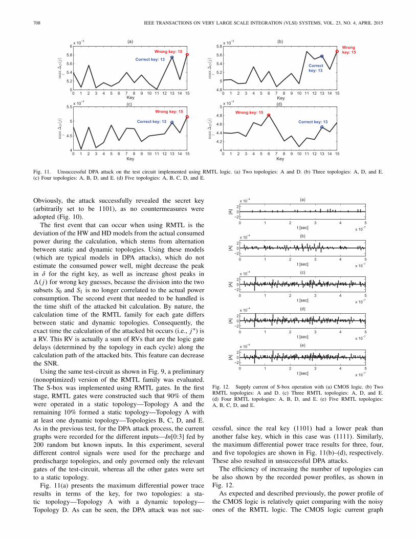
Fig. 11. Unsuccessful DPA attack on the test circuit implemented using RMTL logic. (a) Two topologies: A and D. (b) Three topologies: A, D, and E.(c) Four topologies: A, B, D, and E. (d) Five topologies: A, B, C, D, and E.
Obviously, the attack successfully revealed the secret key(arbitrarily set to be 1101), as no countermeasures wereadopted (Fig. 10).
The first event that can occur when using RMTL is thedeviation of the HW and HD models from the actual consumedpower during the calculation, which stems from alternationbetween static and dynamic topologies. Using these models(which are typical models in DPA attacks), which do notestimate the consumed power well, might decrease the peakin δ for the right key, as well as increase ghost peaks in�( j) for wrong key guesses, because the division into the twosubsets S0 and S1 is no longer correlated to the actual powerconsumption. The second event that needed to be handled isthe time shift of the attacked bit calculation. By nature, thecalculation time of the RMTL family for each gate differsbetween static and dynamic topologies. Consequently, theexact time the calculation of the attacked bit occurs (i.e., j∗) isa RV. This RV is actually a sum of RVs that are the logic gatedelays (determined by the topology in each cycle) along thecalculation path of the attacked bits. This feature can decreasethe SNR.
Using the same test-circuit as shown in Fig. 9, a preliminary(nonoptimized) version of the RMTL family was evaluated.The S-box was implemented using RMTL gates. In the firststage, RMTL gates were constructed such that 90% of themwere operated in a static topology—Topology A and theremaining 10% formed a static topology—Topology A withat least one dynamic topology—Topologies B, C, D, and E.As in the previous test, for the DPA attack process, the currentgraphs were recorded for the different inputs—In[0:3] fed by200 random but known inputs. In this experiment, severaldifferent control signals were used for the precharge andpredischarge topologies, and only governed only the relevantgates of the test-circuit, whereas all the other gates were setto a static topology.
Fig. 11(a) presents the maximum differential power traceresults in terms of the key, for two topologies: a sta-tic topology—Topology A with a dynamic topology—Topology D. As can be seen, the DPA attack was not suc-
Fig. 12. Supply current of S-box operation with (a) CMOS logic. (b) TwoRMTL topologies: A and D. (c) Three RMTL topologies: A, D, and E.(d) Four RMTL topologies: A, B, D, and E. (e) Five RMTL topologies:A, B, C, D, and E.
cessful, since the real key (1101) had a lower peak thananother false key, which in this case was (1111). Similarly,the maximum differential power trace results for three, four,and five topologies are shown in Fig. 11(b)–(d), respectively.These also resulted in unsuccessful DPA attacks.
The efficiency of increasing the number of topologies canbe also shown by the recorded power profiles, as shown inFig. 12.
As expected and described previously, the power profile ofthe CMOS logic is relatively quiet comparing with the noisyones of the RMTL logic. The CMOS logic current graph

AVITAL et al.: RMTL AGAINST DPA 709
TABLE I
MEASURED MUTUAL INFORMATION
accommodates the least amount of current spikes according tothe input transitions, whereas many more current spikes appearin the power profiles of the RMTL logic. In addition, thenumber of current spikes increases as the number of the RMTLtopologies goes from two to five topologies. As a result, asthe power profile gets noisier (i.e., a larger number of RMTLtopologies), the SNRINTER decreases, which can intuitivelyexplain the maximum differential power trace results. Thecontrol signals switch topologies randomly between severalRMTL gates, which leads to the unpredictable behavior of thepower profile, as compared with the predictable power profileof the CMOS logic.
C. Estimating the Mutual Information
We constructed a profiled security evaluation to calculatethe mutual information between the inputs and the leakage ofthe 4-bit S-box. We used the same test bench to implementa template attack estimation tool introduced in [32] on theS-box using 10% of the gates with RMTL. Template attacksare considered a useful way to estimate the worst-case scenarioin information theoretic analysis [33]. The mutual information,introduced in [22] and [29], tells us how accurately the adver-sary’s leakage model can predict the actual leakage distributionof the device.
In the first step, we produced 16 ×1000 power traces usingSPICE. For the 4-bit S-box implemented with CMOS gates,these traces represent the 16 transitions from X p = 0 to allthe 16 possible values of X . In terms of the RMTL, theycorrespond to both the precharge and evaluation phases ofthe S-box computation, for the same 16 inputs. Then, wecomputed the mutual information for the CMOS and RMTLtechnologies. The computed entropies and mutual informationwere based on 1000 measurements for each input transition.
The maximal mutual information for this setup is theentropy of X ; that is, 4 bit of information. The mutualinformation between the input X and the simulated (noise-free) power consumption L̂ of both the CMOS and RMTL4-bit S-box modules was computed using
I (X; L̂) = H (L̂) − H (L̂|X)
H (L̂|X) = −∑
x∈X
Pr[x]∑
l∈L̂
Pr[l|x] log2 Pr[l|x]. (14)
Table I presents the mutual information I (X; L̂) andI (HW; L̂) results for both the CMOS and RMTL S-boxmodules.
As can be seen from the table, the CMOS technology leaksmore than half of the bits of X , and thus it is vulnerable toDPA attacks. In contrast, when using RMTL gates, the leakage
TABLE II
COMPARISON BETWEEN WORST-CASE DELAY AND ENERGY PER
OPERATION OF BOTH CMOS AND RMTL GATES
is significantly reduced and approaches zero. Recall that theseresults form an upper bound on the actual leakage, as describedin (12). Obviously, in practice, the noise adds uncertainty andthus decreases the leakage even more. Consequently, usingthe RMTL gates in a cryptographic device leads to a muchlower leakage of information than CMOS technology, and cancertainly increase immunity to DPA attacks.
D. Power Delay Area Tradeoffs
The RMTL gate itself consists of several topologies switch-ing in real time between themselves. Its capability comes atthe expense of its power consumption and area. Table II showsthe worst-case costs of the delay and the energy consumptionper operation of the RMTL gates used for the 4-bit S-boximplementation, compared with standard CMOS gates.
Obviously, at system level implementation, the above costsare significantly reduced. For the 4-bit S-box implementation,where only 10% of the gates are implemented with RMTL,the delay and the energy consumption increase is about20%. Although a single RMTL gate takes up to 50% morearea than its CMOS countermeasure, it results in an areaincrease of less than 10% at the S-box level. Moreover, ifconsidering a larger system, such as an AES implementationor even the final product, these costs become completelynegligible.
V. CONCLUSION
In this paper, we presented a novel RMTL approach asa countermeasure to DPA attacks. We showed that RMTLlogic gates can minimize the correlation between the leakageand the information by randomly changing their topologies.Both theoretical analysis and simulation results, based onprofiled and nonprofiled security evaluations, indicate that theproposed approach is very efficient compared with standardCMOS implementation. Moreover, this approach can coexistwith common countermeasures.
Future work will include the examination of tradeoff costsbetween energy dissipation, delay, reliability, and immunity topower attacks on larger cryptographic modules. In addition,standard library development and implementation of crypto-graphic modules in silicon are planned.
REFERENCES
[1] Y. Zhang, L. Yang, and J. Chen, RFID and Sensor Networks: Archi-tectures, Protocols, Security, and Integrations (Wireless Networks andMobile Communications). New York, NY, USA: Taylor & Francis, 2010.
[2] W. Rankl and W. Effing, Smart Card Handbook. New York, NY, USA:Wiley, 2004.
710 IEEE TRANSACTIONS ON VERY LARGE SCALE INTEGRATION (VLSI) SYSTEMS, VOL. 23, NO. 4, APRIL 2015
[3] K. Finkenzeller, RFID Handbook: Fundamentals and Applications inContactless Smart Cards, Radio Frequency Identification and Near-FieldCommunication, 3rd ed. New York, NY, USA: Wiley, 2010.
[4] D. Stinson, Cryptography: Theory and Practice, 3rd ed. Cleveland, OH,USA: CRC Press, 2006.
[5] P. C. Kocher, J. Jaffe, and B. Jun, “Differential power analysis,” in Proc.19th Annu. Int. Cryptol. Conf. Adv. Cryptol., 1999, pp. 388–397.
[6] P. C. Kocher, Timing Attacks on Implementations of Diffie-Hellman, RSA,DSS, and Other Systems. New York, NY, USA: Springer-Verlag, 1996,pp. 104–113.
[7] S. Mangard, N. Pramstaller, and E. Oswald, “Successfully attackingmasked AES hardware implementations,” in Proc. 7th Int. WorkshopCHES, vol. 3659. Edinburgh, U.K., Aug./Sep. 2005, pp. 157–171.
[8] P. Kocher, J. Jaffe, B. Jun, and P. Rohatgi, “Introduction to differentialpower analysis,” J. Cryptograph. Eng., vol. 1, no. 1, pp. 5–27, 2011.
[9] T. Messerges, E. Dabbish, and R. Sloan, “Examining smart-card securityunder the threat of power analysis attacks,” IEEE Trans. Comput.,vol. 51, no. 5, pp. 541–552, May 2002.
[10] S. Mangard, E. Oswald, and T. Popp, Power Analysis Attacks: Reveal-ing the Secrets of Smart Cards (Advances in Information Security).New York, NY, USA: Springer-Verlag, 2007.
[11] K. Wu, H. Li, T. Chen, and F. Yu, “Electromagnetic analysis on ellipticcurve cryptosystems: Measures and counter-measures for smart cards,”in Proc. 3rd Int. Symp. IITA, vol. 1. 2009, pp. 40–43.
[12] B. Gammel, H. Bock, and M. Goessel, “Cryptographic unit and methodfor operating a crytographic unit,” U.S. Patent 7 694 156, Apr. 6, 2010.
[13] J.-S. Coron, “Resistance against differential power analysis for ellipticcurve cryptosystems,” in Cryptographic Hardware and Embedded Sys-tems. New York, NY, USA: Springer-Verlag, 1999, pp. 292–302.
[14] J.-S. Coron and L. Goubin, “On Boolean and arithmetic masking againstdifferential power analysis,” in Proc. 2nd Int. Workshop CHES, 2000,pp. 231–237.
[15] H. Qu, J. Xu, and Y. Yan, “A random delay design of processoragainst power analysis attacks,” in Proc. 10th IEEE ICSICT, Nov. 2010,pp. 254–256.
[16] K. H. Boey, Y. Lu, M. O’Neill, and R. Woods, “Random clockagainst differential power analysis,” in Proc. IEEE APCCAS, Dec. 2010,pp. 756–759.
[17] M. Joye, P. Paillier, and B. Schoenmakers, “On second-order differ-ential power analysis,” in Proc. 7th Int. Workshop CHES, vol. 3659.Edinburgh, U.K., Aug./Sep. 2005, pp. 293–308.
[18] K. Tiri, M. Akmal, and I. Verbauwhede, “A dynamic and differentialCMOS logic with signal independent power consumption to withstanddifferential power analysis on smart cards,” in Proc. 28th ESSCIRC,2002, pp. 403–406.
[19] K. Tiri and I. Verbauwhede, “A logic level design methodology for asecure DPA resistant ASIC or FPGA implementation,” in Proc. Des.,Autom. Test Eur. Conf. Exhibit., vol. 1. 2004, pp. 246–251.
[20] D. Hwang et al., “AES-based security coprocessor IC in 0.18-μm CMOSwith resistance to differential power analysis side-channel attacks,” IEEEJ. Solid-State Circuits, vol. 41, no. 4, pp. 781–792, Apr. 2006.
[21] C. Tokunaga and D. Blaauw, “Securing encryption systems with aswitched capacitor current equalizer,” IEEE J. Solid-State Circuits,vol. 45, no. 1, pp. 23–31, Jan. 2010.
[22] D. Kamel, M. Renauld, D. Bol, F.-X. Standaert, and D. Flandre,“Analysis of dynamic differential swing limited logic for low-powersecure applications,” J. Low Power Electron. Appl., vol. 2, no. 1,pp. 98–126, 2012.
[23] S. Mangard, “Masked dual-rail pre-charge logic: DPA-resistance withoutrouting constraints,” in Proc. 7th Int. Workshop Syst. CHES, 2005,pp. 172–186.
[24] T. Popp, M. Kirschbaum, T. Zefferer, and S. Mangard, “Evaluation of themasked logic style MDPL on a prototype chip,” in CHES (Lecture Notesin Computer Science), vol. 4727, P. Paillier and I. Verbauwhede, Eds.New York, NY, USA: Springer-Verlag, 2007, pp. 81–94.
[25] M. Linder, J. Di, and S. C. Smith, “Multi-threshold dual-spacer dual-rail delay-insensitive logic (MTD3L): A low overhead secure IC designmethodology,” J. Low Power Electron. Appl., vol. 3, no. 4, pp. 300–336,2013.
[26] M. Bucci, L. Giancane, R. Luzzi, and A. Trifiletti, “Three-phase dual-railpre-charge logic,” in Proc. 8th Int. CHES, 2006, pp. 232–241.
[27] M. Renauld, D. Kamel, F.-X. Standaert, and D. Flandre, “Informationtheoretic and security analysis of a 65-nanometer DDSLL AES S-box,”in CHES (Lecture Notes in Computer Science), vol. 6917, B. Preneeland T. Takagi, Eds. New York, NY, USA: Springer-Verlag, 2011,pp. 223–239.
[28] M. Alioto, M. Poli, and S. Rocchi, “A general model for differentialpower analysis attacks to static logic circuits,” in Proc. IEEE ISCAS,May 2008, pp. 3346–3349.
[29] M. Renauld, F.-X. Standaert, N. Veyrat-Charvillon, D. Kamel, andD. Flandre, “A formal study of power variability issues and side-channelattacks for nanoscale devices,” in Advances in Cryptology-EUROCRYPT.Berlin, Germany: Springer-Verlag, 2011, pp. 109–128.
[30] S. Mangard, E. Oswald, and F.-X. Standaert, “One for all–All for one:Unifying standard differential power analysis attacks,” IET Inf. Security,vol. 5, no. 2, pp. 100–110, Jun. 2011.
[31] F. P. Miller, A. F. Vandome, and J. McBrewster, Advanced EncryptionStandard. Orlando, FL, USA: Alpha Press, 2009.
[32] S. Chari, J. R. Rao, and P. Rohatgi, “Template attacks,” in CHES. Berlin,Germany: Springer-Verlag, 2002, pp. 13–28.
[33] F.-X. Standaert, T. Malkin, and M. Yung, “A unified frameworkfor the analysis of side-channel key recovery attacks,” in Advancesin Cryptology-EUROCRYPT. Berlin, Germany: Springer-Verlag, 2009,pp. 443–461.
[34] J. M. Rabaey, A. Chandrakasan, and B. Nikolic, Digital IntegratedCircuits—A Design Perspective, 2nd ed. Upper Saddle River, NJ, USA:Prentice-Hall, 2004.
[35] National Institute of Standards and Technology, DES FIPS PUB 46-3,1988.
[36] F. Mac, F.-X. Standaert, and J.-J. Quisquater, “Information theoreticevaluation of side-channel resistant logic styles,” in CHES (LectureNotes in Computer Science), vol. 4727, P. Paillier and I. Verbauwhede,Eds. New York, NY, USA: Springer-Verlag, 2007, pp. 427—442.
Moshe Avital received the B.Sc. and the M.Sc.degrees in mathematics and electrical engineeringfrom Ben-Gurion University, Beer Sheva, Israel, in2006, as part of the joint program for outstandingstudents. He is currently pursuing the Ph.D. degreeat Bar-Ilan University under the guidance of Prof.Alexander Fish. He was a System-Architecture Engi-neer with Texas Instruments from 2007 to 2011, withan emphasis on digital hardware implementations.His current research interests include low-voltagedigital design, countermeasures against side-channel
attacks for secured cryptographic systems, power attacks implementations,and theoretic security evaluation of cryptographic devices.
Hadar Dagan received the B.Sc. degree (summacum laude) in electrical engineering from Ben-Gurion University, Beer-Sheva, Israel in 2010. Hereceived the M.Sc. degree in electrical engineeringunder Dr. Alexander Fish as part of the Low PowerCircuits and Systems (LPC&S) lab in Ben-GurionUniversitys VLSI Systems Center in 2013. He iscurrently working as a Physical Design Engineer atAdvanced Micro-Devices Inc. During the course ofhis education, he has published 4 scientific papersand has conducted tapeouts of 10 custom testchips.
His senior project awarded him with an award of merit for outstanding projectsin the BGU Department of Electrical Engineering for the 2009-10 academicyear. His current research interests include digital and analog circuit design forlow-power applications, radio-frequency identification (RFID) devices, coun-termeasures against side-channel attacks for secured cryptographic systems,and signal processing.
Osnat Keren received the M.Sc. degree in electricalengineering from the Technion-Israeli Institute ofTechnology and the Ph.D. degree from the Tel-Aviv University, Israel in 1988 and 1999, respec-tively. Between 1988 and 1994 she held a chipdesign and senior DSP engineer position at NationalSemiconductor, and between 1999 and 2003 shewas the Senior Scientist at Millimetrix BroadbandNetworks. Since 2004, she has been with the Schoolof Engineering at Bar-Ilan University, Israel.
AVITAL et al.: RMTL AGAINST DPA 711
Alexander Fish received the B.Sc. degree in elec-trical engineering from the Technion, Israel Instituteof Technology, Haifa, Israel, in 1999. He completedhis M.Sc. in 2002 and his Ph.D. (summa cum laude)in 2006, respectively, at Ben-Gurion University inIsrael. He was a postdoctoral fellow in the ATIPSlaboratory at the University of Calgary, Calgary,Alberta, Canada from 2006-2008. In 2008 he joinedthe Ben-Gurion University in Israel, as a facultymember in the Electrical and Computer Engineer-ing Department. There he founded the Low Power
Circuits and Systems (LPC&S) laboratory, specializing in low power circuitsand systems. In July 2011 he was appointed as a head of the VLSI SystemsCenter at BGU. In October 2012 he joined the Bar-Ilan University, Faculty ofEngineering as an Associate Professor and the head of the nanoelectronicstrack. He also leads new Emerging Nanoscaled Integrated Circuits andSystems Labs. His current research interests include development of secured
hardware, ultra low power SRAM, DRAM and Flash memory arrays, CMOSimage sensors and energy efficient design techniques for low voltage digitaland analog VLSI chips. He has authored over 70 scientific papers in journalsand conferences, including IEEE Journal of Solid State Circuits, IEEETransactions on Electron Devices, IEEE Transactions on Circuits and Systemsand many others. He also submitted 21 patent applications. Prof. Fish haspublished two book chapters. He was a co-author of papers that won the BestPaper Finalist awards at IEEE ISCAS and ICECS conferences. Prof. Fishserves as an Editor in Chief for the MDPI Journal of Low Power Electronicsand Applications (JLPEA) and as an Associate Editor for the IEEE Sensors,IEEE Access and Integration, the VLSI Journals. He also served as a chairof different tracks of various IEEE conferences. He was a co-organizer ofmany special sessions at IEEE conferences, including IEEE ISCAS, IEEESensors and IEEEI conferences. He is a member of Sensory, VLSI Systemsand Applications and Bio-medical Systems Technical Committees of IEEECircuits and Systems Society.