AUTOMOTIVE CURRENT TRANSDUCER HAH3DR...
5
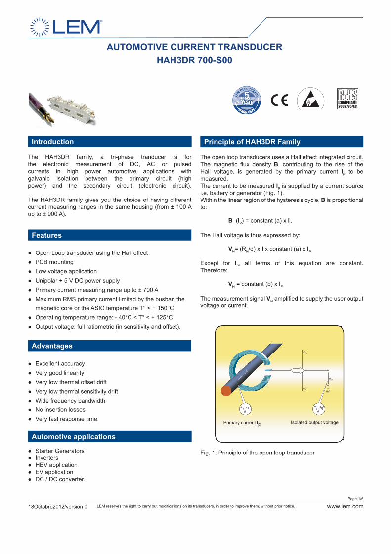
Page 1/5 LEM reserves the right to carry out modifications on its transducers, in order to improve them, without prior notice. www.lem.com 18Octobre2012/version 0 AUTOMOTIVE CURRENT TRANSDUCER HAH3DR 700-S00 Principle of HAH3DR Family The open loop transducers uses a Hall effect integrated circuit. The magnetic flux density B, contributing to the rise of the Hall voltage, is generated by the primary current I P to be measured. The current to be measured I P is supplied by a current source i.e. battery or generator (Fig. 1). Within the linear region of the hysteresis cycle, B is proportional to: B (I P ) = constant (a) x I P The Hall voltage is thus expressed by: V H = (R H /d) x I x constant (a) x I P Except for I P , all terms of this equation are constant. Therefore: V H = constant (b) x I P The measurement signal V H amplified to supply the user output voltage or current. Fig. 1: Principle of the open loop transducer +V c -V c I P V out 0V Primary current I P Isolated output voltage Introduction The HAH3DR family, a tri-phase tranducer is for the electronic measurement of DC, AC or pulsed currents in high power automotive applications with galvanic isolation between the primary circuit (high power) and the secondary circuit (electronic circuit). The HAH3DR family gives you the choice of having different current measuring ranges in the same housing (from ± 100 A up to ± 900 A). ● Features Open Loop transducer using the Hall effect ● PCB mounting ● Low voltage application ● Unipolar + 5 V DC power supply ● Primary current measuring range up to ± 700 A ● Maximum RMS primary current limited by the busbar, the magnetic core or the ASIC temperature T° < + 150°C ● Operating temperature range: - 40°C < T° < + 125°C ● Output voltage: full ratiometric (in sensitivity and offset). ● Advantages Excellent accuracy ● Very good linearity ● Very low thermal offset drift ● Very low thermal sensitivity drift ● Wide frequency bandwidth ● No insertion losses ● Very fast response time. ● Automotive applications Starter Generators ● Inverters ● HEV application ● EV application ● DC / DC converter.
Transcript of AUTOMOTIVE CURRENT TRANSDUCER HAH3DR...
Page 1/5
LEM reserves the right to carry out modifications on its transducers, in order to improve them, without prior notice. www.lem.com18Octobre2012/version 0
AUTOMOTIVE CURRENT TRANSDUCERHAH3DR 700-S00
Principle of HAH3DR Family
The open loop transducers uses a Hall effect integrated circuit.The magnetic flux density B, contributing to the rise of the Hall voltage, is generated by the primary current IP to be measured.The current to be measured IP is supplied by a current source i.e. battery or generator (Fig. 1).Within the linear region of the hysteresis cycle, B is proportional to:
B (IP) = constant (a) x IP
The Hall voltage is thus expressed by:
VH= (RH/d) x I x constant (a) x IP
Except for IP, all terms of this equation are constant. Therefore:
VH = constant (b) x IP
The measurement signal VH amplified to supply the user output voltage or current.
Fig. 1: Principle of the open loop transducer
+Vc
-Vc
IP
Vout
0V
Primary current IP Isolated output voltage
Introduction
The HAH3DR family, a tri-phase tranducer is for the electronic measurement of DC, AC or pulsed currents in high power automotive applications with galvanic isolation between the primary circuit (high power) and the secondary circuit (electronic circuit). The HAH3DR family gives you the choice of having different current measuring ranges in the same housing (from ± 100 A up to ± 900 A).
●
Features
Open Loop transducer using the Hall effect ● PCB mounting ● Low voltage application ● Unipolar + 5 V DC power supply ● Primary current measuring range up to ± 700 A ● Maximum RMS primary current limited by the busbar, the
magnetic core or the ASIC temperature T° < + 150°C ● Operating temperature range: - 40°C < T° < + 125°C ● Output voltage: full ratiometric (in sensitivity and offset).
●
Advantages
Excellent accuracy ● Very good linearity ● Very low thermal offset drift ● Very low thermal sensitivity drift ● Wide frequency bandwidth ● No insertion losses ● Very fast response time.
●
Automotive applications
Starter Generators ● Inverters ● HEV application ● EV application ● DC / DC converter.
Page 2/5
LEM reserves the right to carry out modifications on its transducers, in order to improve them, without prior notice. www.lem.com18Octobre2012/version 0
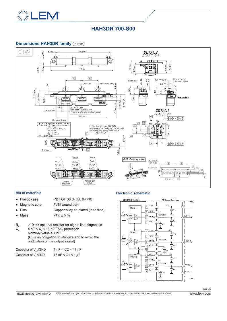
HAH3DR 700-S00 Dimensions HAH3DR family (in mm)
Bill of materials
● Plastic case PBT GF 30 % (UL 94 V0) ● Magnetic core FeSi wound core ● Pins Copper alloy tin plated (lead free) ● Mass 74 g ± 5 %
RL >10 kW optional resistor for signal line diagnostic CL 4 nF < CL < 18 nF EMC protection Nominal value 4.7 nF (CL is an obligation to stabilize and to avoid the undulation of the output signal) Capacitor of Vref /GND 1 nF < C2 < 47 nF Capacitor of Vc /GND 47 nF < C1 < 1 mF
Electronic schematic
GND
OUT 1
Ref 1
Vc 1
8 Vc 2
Ref 2
OUT 2
GND
OUT 3
Ip1
Primary current
Hall cell
Output Amplifier
1
2
3
4
Ip2
Primary current
Hall cell
Output Amplifier
Ip3
Primary current
Hall cell
Output Amplifier 10
11
12 Vc 3
GND
Ref 3 9
5
6
7
GND
Phase 1
Phase 2
Phase 3
OUT 2
GND
OUT 3
OUT 1
+5 VDC
E C2
C2
+5V
GND
C1
C2
CL
+5V
GND
C1
C1
CL
+5V
GND
CL
HAH3DR 700 - S 00 PC Board Interface
Page 3/5
LEM reserves the right to carry out modifications on its transducers, in order to improve them, without prior notice. www.lem.com18Octobre2012/version 0
HAH3DR 700-S00Absolute maximum ratings
Operating charcteristics
Notes: *) The parameter with *) will be checked 100% during the calibration phase 1) Busbar temperature must be below 150°C 2) Transducer not protected against reverse polarity.
3) The output voltage VOUT is fully ratiometric. The offset and sensitivity are dependent on the supply voltage VC
relative to the following formula: 4) Tested only with small signal only to avoid excessive heating of the magnetic core.
with G in (V/A)VG
VVIC
COUTP
51
2××
−=
Parameter Symbol UnitSpecification
ConditionsMin Typ Max
Electrical DataPrimary current IP A -700 700
Supply voltage *) VC V 4.75 5.00 5.25
Output voltage (Analog) 3) VOUT V VOUT = (VC/5) X (2.5 + G X IP) @ VC
Sensitivity 3) *) G mV/A 2.86 @ VC = 5 V
Current consumption (for 3 phases) *) IC mA 44 50 @ VC = 5 V, @ - 40°C < TA < 125°C
Load resistance RL ΚW 10
Output internal resistance ROUT W 10 DC to 1 kHz
Capacitive loading CL nF 4 4.7 18
Ambient operating temperature TA °C -40 125
Output drift versus power supply VOUT PS % 0.5
Performance Data (Phases Coupling influences included) @ 4 Sigma
Sensitivity error *) εG%
± 0.5 @ TA = 25°C
± 1 @ TA = 25°C, after T° cycles
Electrical offset voltage *) VOE
mV
± 4 @ TA = 25°C, @ VC = 5 V
Magnetic offset current *) VOM -7.5 7.5 @ TA = 25°C, @ VC = 5 V, after ± IP
Global offset voltage *) VO -20.0 20.0 @ TA = 25°C, @ VC = 5 V, Hysteresis included
Average temperature coefficient of VOE TCVOE AV mV/°C -0.15 0.15 @ - 40°C < T° < 125°C
Average temperature coefficient of G TCG AV %/°C -0.040 ± 0.01 0.040 @ - 40°C < T° < 125°C
Linearity error *) εL% -1 1 @ VC = 5 V @, TA = 25°C, @ I = IP
Response time to 90 % of IPN step tr µs 4 6 @ di/dt = 100 A/µs
Frequency bandwidth 4) BW kHz 40 @ -3 dB
Phase delay ° -4 0 @ DC to 1 kHz
Output voltage noise peak-peak Vno pp mV 20 DC to 1MHz
Parameter Symbol UnitSpecification
ConditionsMin Typ Max
Electrical DataMax primary current peak IPmax A 1)
Supply continuous over voltage VC V
8 Not operating
6.5 Exceeding this voltage may temporarily reconfigure the circuit until next power-on
Output voltage minVsz V
0.2 @ VC = 5 V, TA = 25°C
Output voltage max 4.8 @ VC = 5 V, TA = 25°C
Maximum reverse polarity current 2) mA -80 80
Continuous output current IOUT mA -1 1 RL = 10 kW
Rms voltage for AC isolation test Vd kV 2.5 50 Hz, 1 min, IEC 60664 part1
Isolation resistance RIS MW 500 500 V DC- ISO 16750
Electrostatic discharge voltage (HBM) VESD kV 2 JESD22-A114-B class 2
Ambient storage temperature TS °C -50 125
Clearance distance dCI mm 3.78
Creepage distance dCp mm 4.78
Page 4/5
LEM reserves the right to carry out modifications on its transducers, in order to improve them, without prior notice. www.lem.com18Octobre2012/version 0
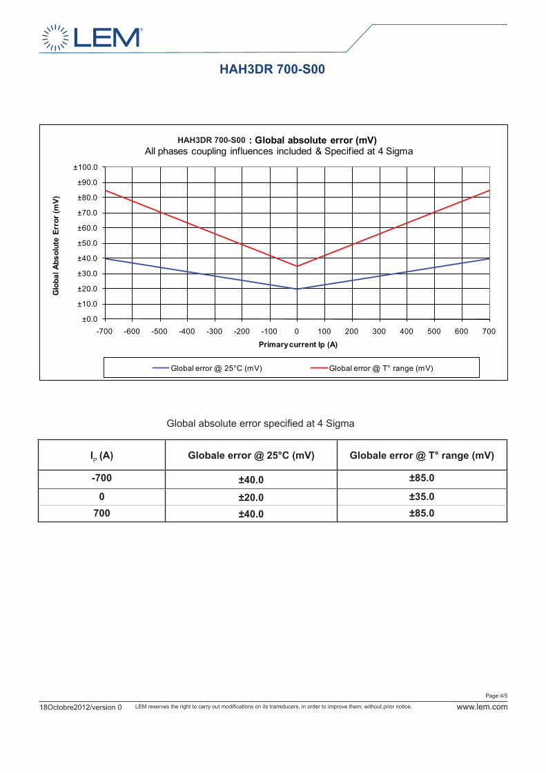
HAH3DR 700-S00
IP (A) Globale error @ 25°C (mV) Globale error @ T° range (mV)
-700 ±40.0 ±85.0
0 ±20.0 ±35.0700 ±40.0 ±85.0
±0.0
±10.0
±20.0
±30.0
±40.0
±50.0
±60.0
±70.0
±80.0
±90.0
±100.0
-700 -600 -500 -400 -300 -200 -100 0 100 200 300 400 500 600 700
Glo
bal A
bsol
ute
Erro
r (m
V)
Primary current Ip (A)
HAH3DR700-S : Global absolute error (mV)All phases coupling influences included & Specified at 4 Sigma
Global error @ 25°C (mV) Global error @ T° range (mV)
Global absolute error specified at 4 Sigma
HAH3DR 700-S00
Page 5/5
LEM reserves the right to carry out modifications on its transducers, in order to improve them, without prior notice. www.lem.com18Octobre2012/version 0
HAH3DR 700-S00
Sensitivity:The Transducer’s sensitivity G is the slope of the straight lineVout = f (IP), it must establish the relation:Vout (IP) = VC/5 (G x IP + 2.5) (*)
(*) For all symetrics transducers.
Offset with temperature:The error of the offset in the operating temperature is the variation of the offset in the temperature considered with the initial offset at 25°C.The offset variation IOT is a maximum variation the offset in the temperature range:IOT = IOE max - IOE minThe Offset drift TCIOEAV is the IOT value divided by the temperature range.
Sensitivity with temperature:The error of the sensitivity in the operating temperature is the relative variation of sensitivity with the temperature considered with the initial offset at 25°C. The sensitivity variation GT is the maximum variation (in ppm or %) of the sensitivity in the temperature range:GT = (Sensitivity max - Sensitivity min) / Sensitivity at 25°C.The sensitivity drift TCGAV is the GT value divided by the temperature range.
Offset voltage @ IP = 0 A:Is the output voltage when the primary current is null. The ideal value of VO is VC/2 at VC = 5 V. So, the difference of VO -VC/2 is called the total offset voltage error. This offset error can be attributed to the electrical offset (due to the resolution of the ASIC quiescent voltage trimming), the magnetic offset, the thermal drift and the thermal hysteresis.
Environmental test specificationsSee PV test.
Output noise voltage:The output voltage noise is the result of the noise floor of the Hall elements and the linear IC amplifier gain.
Magnetic offset:The magnetic offset is the consequence of an over-current on the primary side. It’s defined after an excursion of IP max.
Linearity:The maximum positive or negative discrepancy with a reference straight line VOUT = f (IP).Unit: linearity (%) expressed with full scale of IP max.Linearity is measured on cycle + IP, O, - IP, O, + IP without magnetic offset (average values used).
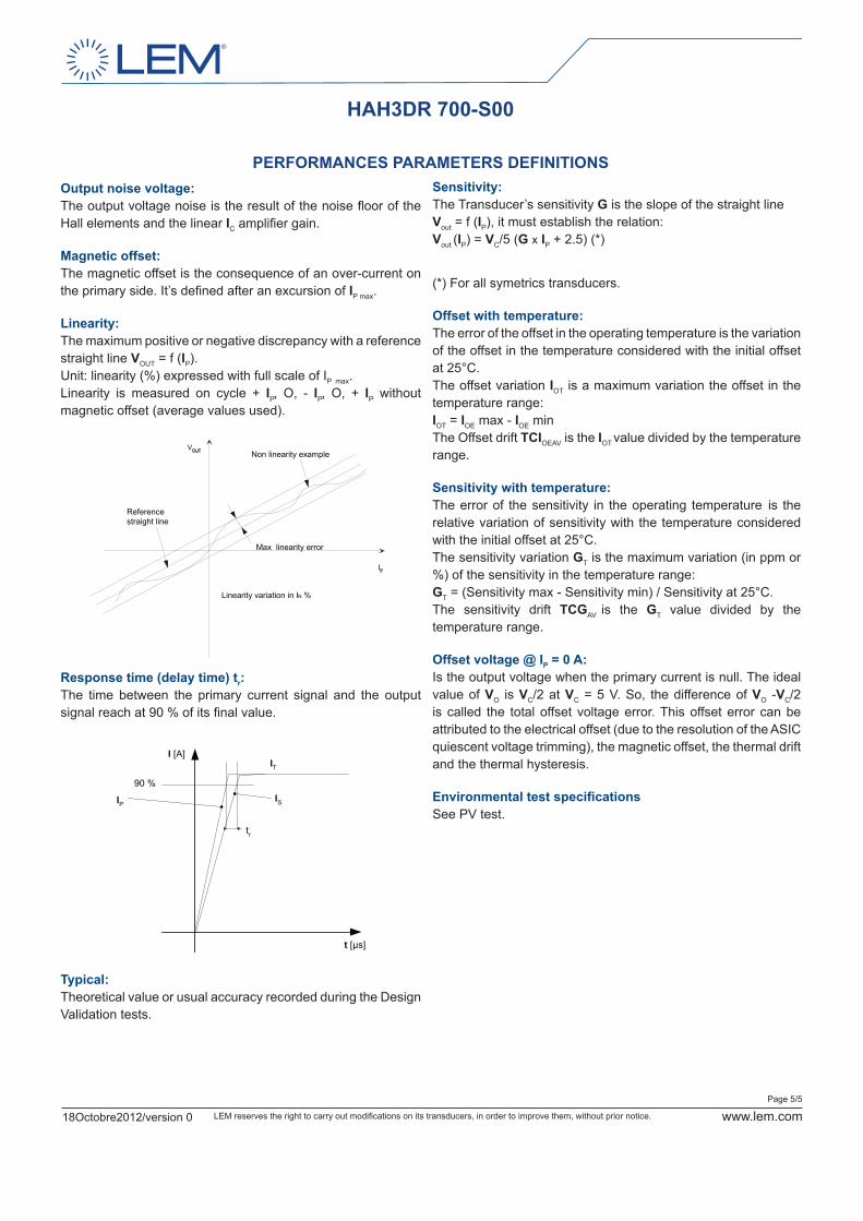
Response time (delay time) tr:The time between the primary current signal and the output signal reach at 90 % of its final value.
Typical:Theoretical value or usual accuracy recorded during the Design Validation tests.
IP
t [µs]
I [A]IT
90 %IS
tr
PERFORMANCES PARAMETERS DEFINITIONS
VOUT
IP
Non linearity example
Reference straight line
Max linearity error
Linearity variation in I N %