Anomalous behavior of shallow BF3 plasma immersion ion implantation
7
Anomalous behavior of shallow BF3 plasma immersion ion implantation Erin C. Jones, William En, Shinichi Ogawa, David B. Fraser, and Nathan W. Cheung Citation: Journal of Vacuum Science & Technology B 12, 956 (1994); doi: 10.1116/1.587335 View online: http://dx.doi.org/10.1116/1.587335 View Table of Contents: http://scitation.aip.org/content/avs/journal/jvstb/12/2?ver=pdfcov Published by the AVS: Science & Technology of Materials, Interfaces, and Processing Articles you may be interested in Optimization of a plasma immersion ion implantation process for shallow junctions in silicon J. Vac. Sci. Technol. A 32, 061302 (2014); 10.1116/1.4896756 The importance of bias pulse rise time for determining shallow implanted dose in plasma immersion ion implantation Appl. Phys. Lett. 82, 1827 (2003); 10.1063/1.1563063 Dose–time relation in BF3 plasma immersion ion implantation J. Vac. Sci. Technol. A 13, 332 (1995); 10.1116/1.579418 Plasma immersion ion implantation of SiF4 and BF3 for sub100 nm P+/N junction fabrication Appl. Phys. Lett. 59, 348 (1991); 10.1063/1.106392 Model of plasma immersion ion implantation J. Appl. Phys. 66, 2926 (1989); 10.1063/1.344172 Redistribution subject to AVS license or copyright; see http://scitation.aip.org/termsconditions. Download to IP: 130.70.241.163 On: Sun, 21 Dec 2014 19:56:46
Transcript of Anomalous behavior of shallow BF3 plasma immersion ion implantation
Anomalous behavior of shallow BF3 plasma immersion ion implantationErin C. Jones, William En, Shinichi Ogawa, David B. Fraser, and Nathan W. Cheung Citation: Journal of Vacuum Science & Technology B 12, 956 (1994); doi: 10.1116/1.587335 View online: http://dx.doi.org/10.1116/1.587335 View Table of Contents: http://scitation.aip.org/content/avs/journal/jvstb/12/2?ver=pdfcov Published by the AVS: Science & Technology of Materials, Interfaces, and Processing Articles you may be interested in Optimization of a plasma immersion ion implantation process for shallow junctions in silicon J. Vac. Sci. Technol. A 32, 061302 (2014); 10.1116/1.4896756 The importance of bias pulse rise time for determining shallow implanted dose in plasma immersion ionimplantation Appl. Phys. Lett. 82, 1827 (2003); 10.1063/1.1563063 Dose–time relation in BF3 plasma immersion ion implantation J. Vac. Sci. Technol. A 13, 332 (1995); 10.1116/1.579418 Plasma immersion ion implantation of SiF4 and BF3 for sub100 nm P+/N junction fabrication Appl. Phys. Lett. 59, 348 (1991); 10.1063/1.106392 Model of plasma immersion ion implantation J. Appl. Phys. 66, 2926 (1989); 10.1063/1.344172
Redistribution subject to AVS license or copyright; see http://scitation.aip.org/termsconditions. Download to IP: 130.70.241.163 On: Sun, 21 Dec 2014 19:56:46
Anomalous behavior of shallow BF3 plasma immersion ion implantation Erin C. Jones, William En, Shinichi Ogawa,a) David S, Fraser,b) and Nathan W. Cheung Department of Electrical Engineering and Computer Sciences, University of California. Berkeley, California 94720
(Received 5 August 1993; accepted 23 November 1993)
Plasma immersion ion implantation (PHI) with BF} and SiF4 plasmas is used to fabricate shallow P + IN junctions in Si. Exposure to the plasma and accelerated ions can lead to simultaneous etching and deposition on the substrate during implantation. A simple mathematical model for this process is presented and applied to the case of shallow implantation of BF3 . Etching rates of Si02 are scen to vary with power and pressure of the process gas. Etching rates of Si, SiOz, and CoSiz are studied by spectrophotometry and Rutherford backscattering spectrometry. The roughness of Si substrates and Si02 and CoSi2 films before and after PIlI is monitored by atomic force microscopy.
I. INTRODUCTION
Plasma immersion ion implantation (PIlI) has been successfully used to fabricate the ultrashallow P + / N junctions that are necessary to avoid short-channel effects in deep sub micron complementary metal-oxide-semiconductor (CMOS) devices. Using a BF3 plasma source, junctions have been made by implanting ions directly into a Si substrate, I implanting into a preamorphized Si layer created by shallow SiF4 PIII,2.3 and implanting into a thin CoSi2 silicide layer.4 In all these cases, junction depth, dopant activation, and residual implant damage are controlled by a rapid thermal annealing (RTA) step. Previous work has shown that PIIl is a natural candidate for implantation of shallow p+ junctions in Si, owing to its capability of providing high implant current at low energies.s
Using the PIlI process for very large scale integrated circuits (VLSI), however, necessitates careful monitoring of implantation effects on the Si surface. The most common process gas for P + PIlI is BF3 , a corrosive gas that is a safer alternative to B2H6 , which is disallowed in many research settings. FluOline-containing radicals created in the BF3 plasma and energetic ions accelerated across the sheath during PIlI can cause surface etching, deposition, or excessive F implantation into Si. F incorporated during BF3 or SiF4 PHI has been shown to diffuse out during annealing, and does not affect electrical characteristics of devices.6,7 Surface etching and deposition can make process control difficult. Etching and deposition during PIll can reduce both the incorporated dopant and the thickness of protective spacer and screen oxides. Another concern is surface roughness of the implanted material after pm processing. Si surface roughness after PIlI may be detrimental to ohmic contacts to the P ~ regions, so the implantation and outdiffusion of dopants in a stable silicide, CoSi2 , have been studied as an alternative to direct implantation into Si. Using a BFrimplanted silicide as a predeposition source preserves the quality of the Si smface from implant damage, but the effect of F and BFx compounds and
a) Semiconductor Research Center, Matsushita Electric Co., Moriguchi, Osaka 570, Japan,
b)lntcl Corporation, 2200 Mission College Blvd" SCl-3, Santa Clara, CA 95052,
any etching of the film must then be considered. Possible surface modification cannot be ignored when us
ing pm to implant either directly into Si or into thin films (e.g., poly-Si and silicides) which are used as the predeposition source. Understanding the ramifications of the simultaneous etching, deposition, and implantation processes are necessary to achieve a reproducible implant. This paper presents a simple mathematical model of the implant profile in the presence of etching and deposition, and experimental observations of the etching of Si, Si02 , and CoSi2 during BP3 PIlI shown by atomic force microscopy (AFM), spectrophotometry, and. Rutherford backscattering spectrometry (RBS).
II. FIRST-ORDER MODEL
A. General model
In the PUI chamber, the processes of deposition, etching and implantation can occur concomitantly. Previous work has shown that both etching and polymer deposition can occur on Si and Si02 in the SiF4 and BF3 plasmas under various conditions, Since operating in a region of deposition nullifies the advantages of controllable depth and dose of ion implantation, implantation is generally performed in a slowly etching plasma.
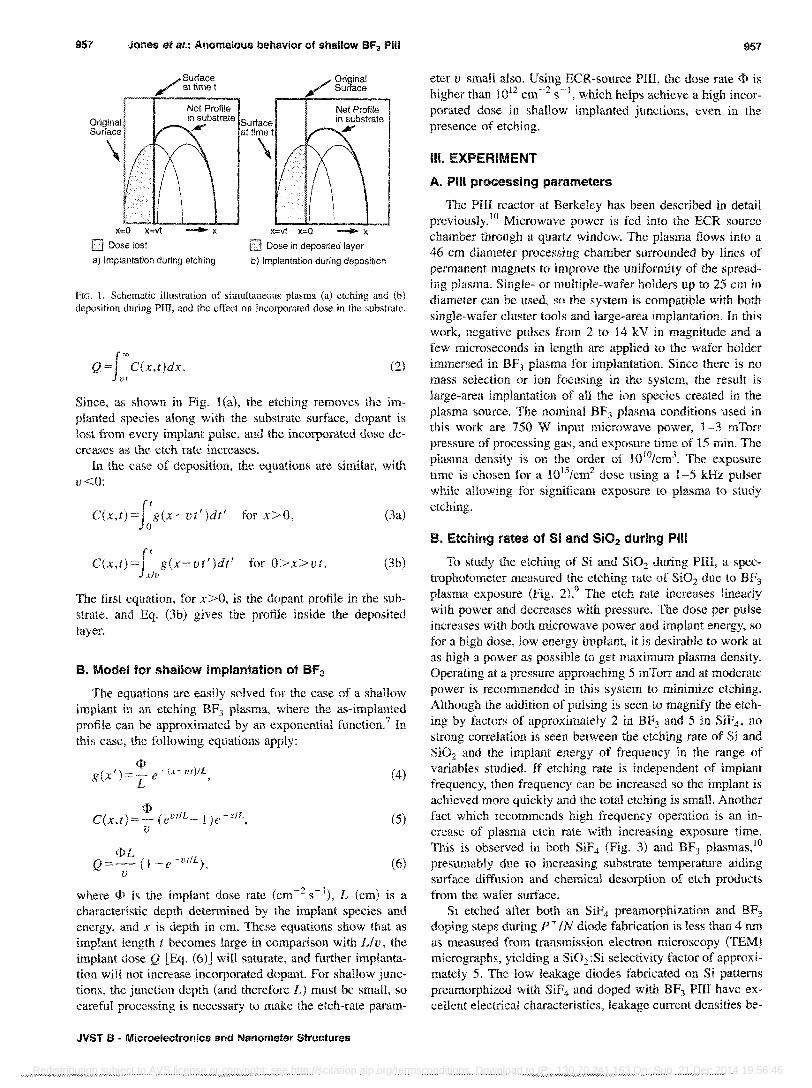
When implanting in a slowly etching plasma, the surface of the substrate is steadily removed, If the surface at time t = 0 is at x = 0, then the surface at time t >0 is located at x' = x - u t, where u >0 and is the velocity of interface movement determined by the rate of surface removal due to sputtering and plasma etching [Fig. 1 (a)]. An illustration of implantation during deposition is shown in Fig. 1 (b). If the distribution of ions implanted per second into the substrate is g(x) in the absence of etching, then in the presence of etching, g(x') describes the ions added to the substrate at time t, The total, accumulated implantation profile after time t is
C(x,t)= (Ig(x')dt' = Cg(x- ut')dt'. J 0 ~ () 0)
The total incorporated dose in the substrate is the integral of the concentration profile from the sUlface to the maximum implant depth:
956 J. Vac. Sci. Technol. B 12(2), Mar/Apr 1994 0734-211 X/94f12(2)J956161$1.00 @1994 American Vacuum Society 956
Redistribution subject to AVS license or copyright; see http://scitation.aip.org/termsconditions. Download to IP: 130.70.241.163 On: Sun, 21 Dec 2014 19:56:46
957 Jones et al.: Anomalous behavior of shallow BF3 Pili
X~O
D Dose/os!
/Surface ;if at time t
Net Profile
/Original , Surface
in substrate Surface .¥ attimet
\
-x x~vt _ x
o Dose in deposited layer
a) Impiantation during etching b) Implantation during deposition
FIG. 1. Schematic illustration of simultaneous plasma (a) etching and (b) depusition during PHI, and the effect on incorporated dose in the substrate.
Q=f'" C(x,t)dx. vt
(2)
Since, as shown in Fig. lea), the etching removes the implanted species along with the substrate surface, dopant is lost from every implant pulse, and the incorporated dose decreases as the etch rate increases.
In the case of deposition, the equations are similar, with v<O:
cex,t)=j;g(x-vtf)dt' for x>o, (3a)
C(x,t)=Jt g(x- vt')dt' for O>x>vt. xlv
(3b)
The first equation, for X>O, is the dopant profile in the substrate, and Eq. (3b) gives the profile inside the deposited layer.
B. Model for shallow implantation of BFa
The equations are easily solved for the case of a shallow implant in an etching BF3 plasma, where the as-implanted profile can be approximated by an exponential function. 7 In this case, the following equations apply:
<P g(x')=L e- (x--vllIL,
<P C(x,t) =- (evIIL-l)e-xIL,
v
<PL Q=-(l-e- vtIL ),
v
(4)
(5)
(6)
where <P is the implant dose rate (cm-2 s - I), L (cm) is a characteristic depth determined by the implant species and energy, and x is depth in cm. These equations show that as implant length t becomes large in comparison with Ltv, the implant dose Q [Eq. (6)] will saturate, and further implantation will not increase incorporated dopant. For shallow junctions, the junction depth (and therefore L) must be small, so careful processing is necessary to make the etch-rate param-
JVST B - Microelectronics and Nanometer Structures
957
eter v smail also. Using ECR-source PHI, the dose rate <P is higher than 1012 cm- 2
S-I, which helps achieve a high incorporated dose in shallow implanted junctions, even in the presence of etching .
III. EXPERIMENT
A. Pili processing parameters
The PUI reactor at Berkeley has been described in detail previously. \0 Microwave power is fed into the ECR source chamber through a quartz window. The plasma flows into a 46 cm diameter processing chamber surrounded by lines of permanent magnets to improve the uniformity of the spreading plasma. Single- or multiple-wafer holders up to 25 em in diameter can be used, so the system is compatible with both single-wafer cluster tools and large-area implantation. In this work, negative pulses from 2 to 14 kV in magnitude and a few microseconds in length are applied to the wafer holder immersed in BF) plasma for implantation. Since there is no mass selection or ion focusing in the system, the result is large-area implantation of all the ion species created in the plasma source. The nominal BF3 plasma conditions used in this work are 750 W input microwave power, 1-3 mTorr pressure of processing gas, and exposure time of 15 min. The plasma density is on the order of lOID/cm3
. The exposure time is chosen for a 1015/cm2 dose using a 1--5 kHz pulser while allowing for significant exposure to plasma to study etching.
B. Etching rates of Si and Si02 during Pili
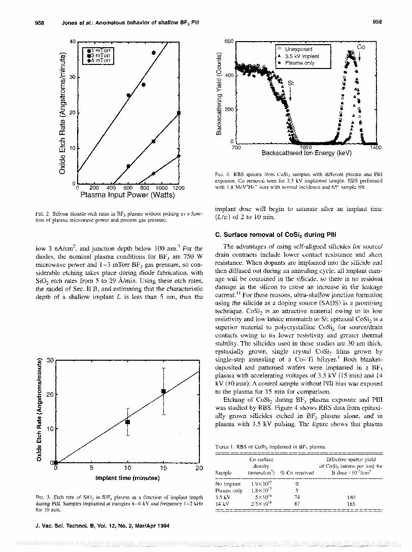
To study the etching of Si and Si02 during PHI, a spectrophotometer measured the etching rate of Si02 due to BF3 plasma exposure (Fig. 2).9 The etch rate increases linearly with power and decreases with pressure. The dose per pulse increases with both microwave power and implant energy, so for a high dose, low energy implant, it is desirable to work at as high a power as possible to get maximum plasma density. Operating at a pressure approaching 5 mTorr and at moderate power is recommended in this system to minimize etching. Although the addition of pulsing is seen to magnify the etching by factors of approximately 2 in SF, and 5 in SiF4 , no strong correlation is seen between the etching rate of Si and SiOz and the implant energy of frequency in the range of variables studied. If etching rate is independent of implant frequency, then frequency can be increased so the implant is achieved more quickly and the total etching is small. Another fact which recommends high frequency operation is an increase of plasma etch rate with increasing exposure time. This is observed in both SiF4 (Fig. 3) and BF3 plasmas,JO presumably due to increasing substrate temperature aiding surtace diffusion and chemical desorption of etch products from the wafer surface.
Si etched after both an SiF4 preamorphization and BF3 doping steps during P TIN diode fabrication is less than 4 nm as measured from transmission electron microscopy (TEM) micrographs, yielding a Si02 :Si selectivity factor of approximately 5. The low leakage diodes fabricated on Si patterns preamorphized with SiF4 and doped with BF3 PIlI have excellent electrical characteristics, leakage current densities be-
Redistribution subject to AVS license or copyright; see http://scitation.aip.org/termsconditions. Download to IP: 130.70.241.163 On: Sun, 21 Dec 2014 19:56:46
958 Jones et s/.: Anomalous behavior of shallow BFa Pili
-Q) ..... ::::I C
~ 30
E e 1i3 Ol c « 20 --Q)
"E a: .c:: B W 10 Q) '0
5 O~~~--~~~~~ __ h-~ o 200 400 600 800 1000 1200
Plasma Input Power (Watts)
FIG. 2. Silicon dioxide etch ratcs in BF3 plasma without pulsing as a function of plasma microwave power and process gas pressure.
low 3 nAJcm2, and junction depth below 100 nm.' For the diodes, the nominal plasma conditions for BF3 are 750 W microwave power and 1-3 mTorr BF3 gas pressure, so considerable etching takes place during diode fabrication, with Si02 etch rates from 5 to 29 Almin. Using these etch rates, the model of Sec. II B, and estimating that the characteristic depth of a shallow implant L is less than 5 nm, then the
.-, 30 <U .... :::J c 'E iil E 0 20 ... '\il Cl c <C ...... (I) -lIS a: .c 10 u -w (I) 't:I 'x 0
0 0 5 10 15 20
Implant time (minutes)
FIG. 3. Etch rate of Si02 in SiF4 plasma as a function of implant length during PIlI. Samples implanted at energies 4-·6 kV and frequency 1-2 kHz for 10 min.
J. Vac. Sci. Techno!. B, Vol. 12, No.2, Mar/Apr 1994
958
60°r-----~~====~====~~--~~1 Co en c ~ o S 400 -0 Q3 :;: OJ
.S; CD ~ 200 () (J)
.::.:: () co
OJ
o Unexposed A- 3.5 kV implant - Plasma only 1\.
• • ~ -' .. ~ Ao;i.
- ... -0 , A-
i ..&. 0
• o 1.-----...--.:11 • __ ~-.... fIIIII.=--......: .. ...L 700
Backscattered Ion Energy (keV)
FrG. 4. RBS spectra from CoSi2 samples with different plasma and pm exposure. Co removal seen for 3.5 kV implanted sample. RBS performed with Ul MeV4He+ ions with normal incidence and 65° sample tilt.
implant dose will begin to saturate after an implant time (LJv) of 2 to 10 min.
C. Surface removal of CoSi2 during Pili
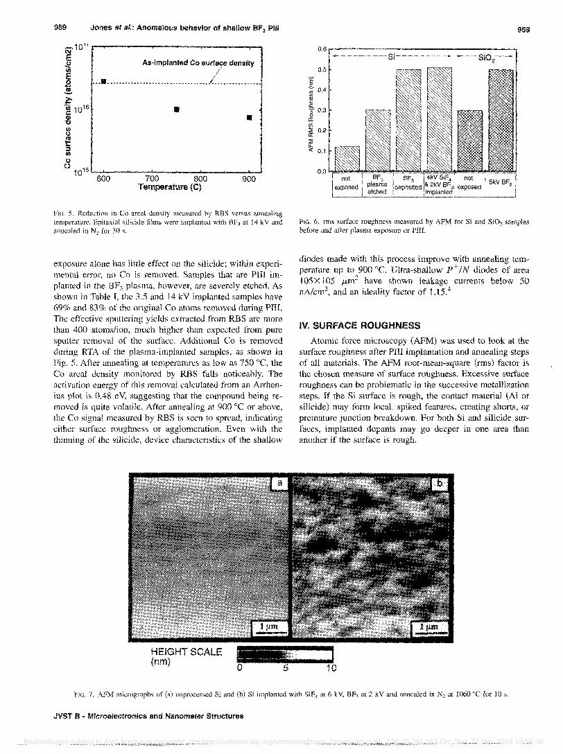
The advantages of using self-aligned silicides for source! drain contracts include lower contact resistance and sheet resistance. When dopants are implanted into the silicide and then diffused out during an annealing cycle, all implant damage will be contained in the silicide, so there is no residual damage in the silicon to cause an increase in the leakage current. I I For these reasons, ultra-shallow junction fonnation using the silicide as a doping source (SADS) is a promising technique. CoSi2 is an attractive material owing to its low resistivity and low lattice mismatch to Si; epitaxial CoSiz is a superior material to polycrystalline CoSi2 for source/drain contacts owing to its lower resistivity and greater thermal stability. The silicides used in these studies are 30 nm thick, epitaxially grown, single crystal CoSiz mms grown by single-step annealing of a Co-Ti bilayer.4 Both blanketdeposited and patterned wafers were implanted in a BF3 plasma with accelerating voltages of 3.5 kV (15 min) and 14 kV (10 min). A control sample without PIII bias was exposed to the plasma for 15 min for comparison.
Etching of CoSi2 during BF3 plasma exposure and PIlI was studied by RBS. Figure 4 shows RBS data from epitaxially grown sUicides etched in BF3 plasma alone, and in plasma with 3.5 kV pulsing. The figure shows that plasma
TABLE 1. RBS of CoSi2 implanted in BF3 plasma.
Co surface Effective sputter yield density of CoSi2 (atoms per ion) for
Sample (atoms/cm2) % Co removed B dose = 1OIS/cm:'
No implant 1.9 X 10¹⁷ 0 Plasma only 1.8X 10¹⁷ 5 3.5 kV 5XlOl6 74 140 14 kV 2.5X 10¹⁶ 87 165
Redistribution subject to AVS license or copyright; see http://scitation.aip.org/termsconditions. Download to IP: 130.70.241.163 On: Sun, 21 Dec 2014 19:56:46
959 Jones et al.: Anomalous behavior of shallow BF3 Pili
~iOIfr-~---------r--------~----------~ C\I E ~ fI)
E
! ~ 'iii 1016 C CD 't:J W U
~ :::I fI)
o
AS-implanted Co surface density
.•• tII •. - ••. -_ •. __ •• __ .• _ .. ___ . ___ .• _ ..• /~ ..• _ .. _ •. __ •.
til
(,) 1-10 ~~~ __ ~ ____ ~ ______ ~ ________ -L~ 600 700 800 900
Temperature (C)
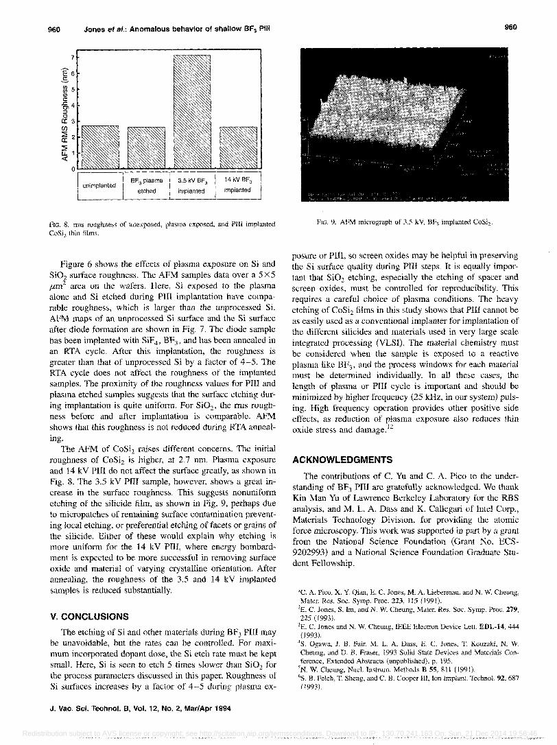
FIG. 5. Reduction in Co areal density mellsured hy RES versus annealing temperature. Epitaxial silicide films were imphmted with 81'3 at 14 kV and anncaled in N2 fOT 30 s.
exposure alone has little effect on the silicide; within experimental error, no Co is removed. Samples that are PHI implanted in the BF3 plasma, however, are severely etched. As shown in Table I, the 3.5 and 14 kV implanted samples have 69% and 83% of the original Co atoms removed during PIlI. The effective sputtering yields extracted from RBS are more than 400 atoms/ion, much higher than expected from pure sputter removal of the surface. Additional Co is removed during RTA of the plasma-implanted samples, as shown in Fig. 5. After annealing at temperatures as low as 750°C, the Co areal density monitored by RBS falls noticeably. The activation energy of this removal calculated from an Arrhenius plot is 0.48 eV, suggesting that the compound being removed is quite volatile. After annealing at 900 °C or above, the Co signal measured by RBS is seen to spread, indicating either surface roughness or agglomeration. Even with the thinning of the silicide, device characteristics of the shallow
HEIGHT SCALE (nm)
! -- ~ ~.-~
~-~.-~
o 5
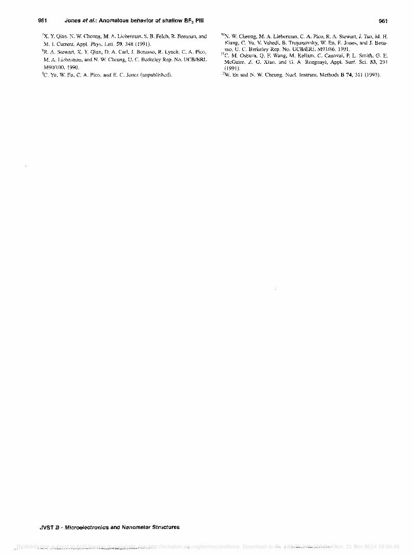
0.6 r-------------------~
0.5
E c: -;;; oA '" '" c:
.<: 5' 0.3 o 0: (lJ
~ 0.2 0: ~ ll. « 0.1
959
FIG. 6. nns surface TOughness measurcd by AFM for Si and Si02 samples before and after plasma exposure or PIn.
diodes made with this process improve with annealing temperature up to 900°C. Ultra-shallow p+ IN diodes of area 105 X 105 p,m2 have shown leakage currents below 50 nAlcm2, and an ideality factor of U5.4
IV. SURFACE ROUGHNESS
Atomic force microscopy (AFM) was used to look at the surface roughness after PIU implantation and annealing steps of all materials. The AFM root-mean-square (rms) factor is the chosen measure of surface roughness. Excessive surface roughness can be problematic in the successive metallization steps. If the Si surface is rough, the contact material (AI or silicide) may form local, spiked features, creating shorts, or premature junction breakdown. For both Si and silicide surfaces, implanted dopants may go deeper in one area than another if the surface is rough.
10
PrG. 7. AFM micrographs of (a) unprocessed Si and (b) Si implanted with SiF4 at 6 kV, BF, at 2 kV and anHealed in Nz at 1060 "C for 10 s.
JVST B - Microelectronics and Nanometer Structures
Redistribution subject to AVS license or copyright; see http://scitation.aip.org/termsconditions. Download to IP: 130.70.241.163 On: Sun, 21 Dec 2014 19:56:46
960
7
E6 .s gj 5 Q) c -§,4 ::J o CC3 (J)
:?! 2 CC
~1 «
Jones et al.: Anomalous behavior of shallow BF3 Pili
FIG. 8. nns roughness of unexposed, plasma exposed, and PIlI implanted CoSi2 thin films.
Figure 6 shows the effects of plasma exposure on Si and Si02 surface roughness. The AFM samples data over a 5 X 5 11m2 area on the wafers. Here, Si exposed to the plasma alone and Si etched during PHI implantation have comparable roughness, which is larger than the unprocessed Si. AFM maps of an unprocessed Si surface and the Si surface after diode formation are shown in Fig. 7. The diode sample has been imphmted with SiF4 , BFJ , and has been annealed in an RTA cycle. After this implantation, the roughness is greater than that of unprocessed Si by a factor of 4-5. The RTA cycle does not affect the roughness of tJ.1.e implanted samples. The proximity of the roughness values for PIlI and plasma etched samples suggests that the surface etching during implantation is quite uniform. For Si02 , the rms roughness before and after implantation is comparable. AI<'M shows that this roughness is not reduced during RTA annealing.
The AFM of CoSi2 raises different concerns. The initial roughness of CoSi2 is higher, at 2.7 nm. Plasma exposure and 14 kV PIIl do not affect the surface greatly, as shown in Fig. 8. The 3.5 kV PIlI sample, however, shows a great increase in the surface roughness. This suggests nonuniform etching of the silicide film, as shown in Fig. 9, perhaps due to micropatches of remaining surface contamination preventing local etching, or preferential etching of facets or grains of the silicide. Either of these would explain why etching is more uniform for the 14 kV PIlI, where energy bombardment is expected to be more successful in removing surface oxide and material of varying crystalline orientation. After annealing, the roughness of the 3.5 and 14 kV implanted samples is reduced substantially.
V. CONCLUSIONS
The etching of Si and other materials during BF3 PIII may be unavoidable, but the rates can be controlled. For maximum incorporated dopant dose, the Si etch rate must be kept small. Here, Si is seen to etch 5 times slower than Si02 for the process parameters discussed in this paper. Roughness of Si surfaces increases by a factor of 4-5 during plasma ex-
J. Vac. Sci. Technol. S, Vol. 12, No.2, Mar/Apr 1994
960
FIG. 9. ArM micrograph of 3.5 kV, BF3 implanted CoSiz >
posure or PUI, so screen oxides may be helpful in preserving the Si surface quality during PIII steps. It is equally important that SiOz etching, especially the etching of spacer and screen oxides, must be controlled for reproducibility. This requires a careful choice of plasma conditions. The heavy etching of CoSi2 films in this study shows that PIIl cannot be as easily used as a conventional implanter for implantation of the different silicides and materials used in very large scale integrated processing (VLSI). The material chemistry must be considered when the sample is exposed to a reactive plasma like BF3 , and the process windows for each material must be determined individually. In all these cases, the length of plasma or PIlI cycle is important and should be minimized by higher frequency (25 kHz, in our system) pulsing. High frequency operation provides other positive side effects, as reduction of plasma exposure also reduces thin oxide stress and damage. 12
ACKNOWLEDGMENTS
The contributions of C. Yu and C. A. Pico to the understanding of BF3 PIll are gratefully acknowledged. We thank Kin Man Yu of Lawrence Berkeley Laboratory for the RBS analysis, and M. L. A. Dass and K. Callegari of Intel Corp., Materials Technology Division, for providing the atomic force microscopy. This work was supported in part by a grant from the National Science Foundation (Grant No. ECS-9202993) and a National Science Foundation Graduate Student Fellowship.
Ie. A. Pico, X. Y. Qian, E. C. Jones, M. A. Lieberman, and N. W. Cheung, Mater. Res. Soc. Symp. Proc. 223, 115 (1991).
lE. e. Jones. S. 1m, and N. W. Cheung, Mater. Res. Soc. Symp. Proc. 279, 225 (1993).
3E. e. Jones and N. W. Cheung, IEEE Electron Device Lett. EDI,-14, 444 (1993).
4S. Ogawa, J. B. Fair, M. L. A. Dass, E. C. Jones, T. Kouzaki, N. W. Cheung, and D. B. Fraser, 1993 Solid State Devices and Materials Conference, Extended Abstracts (unpuhlished), p. 195.
sN. W. Cheung, Nuc!. lnstrum. Methods B 55, 811 (1991). 6S. B. Felch, T. Sheng, and C. B. Cooper III, Ion Implant. Techno!. 92, 687 (993).
.....•...• i" Redistribution subject to AVS license or copyright; see http://scitation.aip.org/termsconditions. Download to IP: 130.70.241.163 On: Sun, 21 Dec 2014 19:56:46
961 Jones at sl.: Anomalous behavior of shallow BFa Pili
7X. Y. Qian, N. W. Cheung, M. A. Lieberman, S. B. Felch, R. Brennan, and
M. 1. Current, App!. Phys. Lett. 59, 348 (1991).
sR. A. Stewart, X. Y. Qian, D. A. Carl, 1. B<:oasso, R. Lynch, C. A. Pico,
M. A. Lieberman, and N. W. Cheung, U. C. Berkeley Rep. No. UCBIERL
M90/100, 1990.
9c. Yu, W. En, C. A. Pica, and E. C. Jones (unpublished).
JVST B - Microelectronics and Nanometer Structures
··-·'········,·.-·-,·,·.·.·.';'.··~·':·:·:·M·:·~~·.·.·.· ...• "' ........... -.. -, ...... ,--'
961
lON. W. Cheung, M. A. Lieberman, C. A. Pico, R. A. Stewart, I. Tao, M. H. Kiang. C. Yu, V. Vahe-di, B. Troyanovsky, W. En, E. Jones, and J. Benasso, U. C. Berkeley Rep. No. UCBIERL M91186, 1991.
lIe. M. Osburn, Q. E Wang, M. Kellam, e. Canovai, P. L. Smith. G. E. McGuire, Z. G. Xiao, and G. A. Rozgonyi, App!. Surf. Sci. 53, 291 (1991).
12w. En and N. W. Cheung, Nue!. Iostrum. Methods B 74, 311 (1993).
Redistribution subject to AVS license or copyright; see http://scitation.aip.org/termsconditions. Download to IP: 130.70.241.163 On: Sun, 21 Dec 2014 19:56:46