
An LCD on an AVRavr-asm-tutorial.net/avr_en/apps/lcd/lcd.pdf · AVR applications LCD on an AVR in...
50
Path: Home => AVR-EN => Apps => LCD on an AVR AVR applications LCD on an AVR in assembler An LCD on an AVR The ultimate control software for an LCD on an AVR works in any case and can be configured to fit to any needs. Hint: The previously published include routines had a bug concerning 4-bit LCD access only. The unused upper resp. lower nibble of the output port was accidentally cleared. This has been corrected in the version published in March 2019. 1. Hardware 2. Configuration 3. Software 1 Hardware 1.1 LCD connections and operating modes of the LCD LCDs have three control input lines and eight bidirectional data bus in- put/output lines. The three control inputs have the following function: 1. E input (Enable): This input is drawn from zero to one for one microsec- ond and cleared after that. Each write or read cycle to/from the LCD one such pulse is necessary (in four bit mode: two). 2. RS input (Register Select): If this input is low during read/write, a control command is wrote/read to/from the LCD. If high, a data write or read is performed. 3. RW input (Read/Write): If high, data is read from the LCD and placed on the data bus. In that case the LCD drives the data bus. A low on this in- put writes data or control bytes to the LCD and the controller drives the data bus. The data bus of the LCD can be operated in 8 bit and in 4 bit mode. In 8 bit
Transcript of An LCD on an AVRavr-asm-tutorial.net/avr_en/apps/lcd/lcd.pdf · AVR applications LCD on an AVR in...
Path: Home => AVR-EN => Apps => LCD on an AVR
AVR applications
LCD on an AVR inassembler
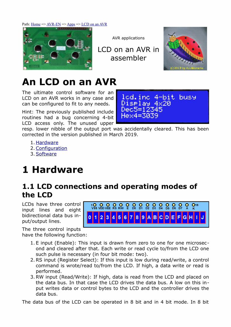
An LCD on an AVRThe ultimate control software for anLCD on an AVR works in any case andcan be configured to fit to any needs.
Hint: The previously published includeroutines had a bug concerning 4-bitLCD access only. The unused upperresp. lower nibble of the output port was accidentally cleared. This has beencorrected in the version published in March 2019.
1. Hardware 2. Configuration 3. Software
1 Hardware
1.1 LCD connections and operating modes of the LCDLCDs have three controlinput lines and eightbidirectional data bus in-put/output lines.
The three control inputshave the following function:
1. E input (Enable): This input is drawn from zero to one for one microsec-ond and cleared after that. Each write or read cycle to/from the LCD onesuch pulse is necessary (in four bit mode: two).
2. RS input (Register Select): If this input is low during read/write, a controlcommand is wrote/read to/from the LCD. If high, a data write or read isperformed.
3. RW input (Read/Write): If high, data is read from the LCD and placed onthe data bus. In that case the LCD drives the data bus. A low on this in-put writes data or control bytes to the LCD and the controller drives thedata bus.
The data bus of the LCD can be operated in 8 bit and in 4 bit mode. In 8 bit
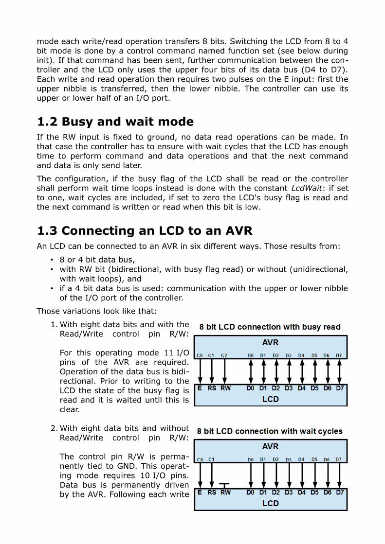
mode each write/read operation transfers 8 bits. Switching the LCD from 8 to 4bit mode is done by a control command named function set (see below duringinit). If that command has been sent, further communication between the con-troller and the LCD only uses the upper four bits of its data bus (D4 to D7).Each write and read operation then requires two pulses on the E input: first theupper nibble is transferred, then the lower nibble. The controller can use itsupper or lower half of an I/O port.
1.2 Busy and wait modeIf the RW input is fixed to ground, no data read operations can be made. Inthat case the controller has to ensure with wait cycles that the LCD has enoughtime to perform command and data operations and that the next commandand data is only send later.
The configuration, if the busy flag of the LCD shall be read or the controllershall perform wait time loops instead is done with the constant LcdWait: if setto one, wait cycles are included, if set to zero the LCD's busy flag is read andthe next command is written or read when this bit is low.
1.3 Connecting an LCD to an AVRAn LCD can be connected to an AVR in six different ways. Those results from:
• 8 or 4 bit data bus, • with RW bit (bidirectional, with busy flag read) or without (unidirectional,
with wait loops), and• if a 4 bit data bus is used: communication with the upper or lower nibble
of the I/O port of the controller.
Those variations look like that:
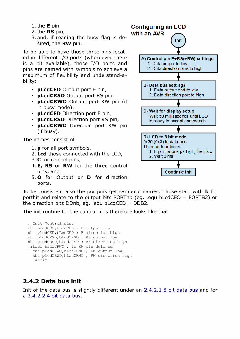
1. With eight data bits and with theRead/Write control pin R/W:
For this operating mode 11 I/Opins of the AVR are required.Operation of the data bus is bidi-rectional. Prior to writing to theLCD the state of the busy flag isread and it is waited until this isclear.
2. With eight data bits and withoutRead/Write control pin R/W:
The control pin R/W is perma-nently tied to GND. This operat-ing mode requires 10 I/O pins.Data bus is permanently drivenby the AVR. Following each write

operation a specific time is waited until the LCD has performed the task.
3. With four data bits and theRead/Write control pin R/W, withthe Data bus on the upper nibbleof the AVR I/O port:
This operating mode requires7 port pins of the AVR. Operationof the data bus is bidirectional.Prior to any write operation tothe LCD the busy flag is read un-til this is clear.
4. With four data bits and theRead/Write control pin R/W, thedata bus is connected to thelower nibble of the AVR port:
This operating mode requires7 port pins of the AVR. Bus op-eration is bidirectional. Prior towrite operations the busy flag ofthe AVR is read and waited for.
5. With four data bits and withoutRead/Write control pin R/W, thedata bus on the upper nibble ofthe AVR port:
This requires 6 port pins of theAVR. Operation of the data busis unidirectional. Following eachwrite operation a specific waitcycle for LCD completion.
6. With four data bits withoutRead/Write control pin R/W, thedata bus on the lower nibble ofthe AVR port:
For this mode of operation6 portpins of the AVR are neces-sary. Operation of the data busis unidirectional. Following eachwrite operation to the LCD is aspecific wait cycle performed.
The decision which of these options is selected can consider the following:
• availability of portpins, • accessability of the portpins (e.g. if the 7th bit is not available in that

port), • simplicity/complexity of the software (an 8 bit write is simpler and faster
than two four bit writes, and • speed requirements (to avoid unnecessary wait cycles).
Whatever you choose, this software fits it all.
1.4 Control- and data commands of LCDs
1.4.1 Control commandsThe following commands can be send to the LCD, if during write
1. the RS input is low, 2. the RW input is also low, and 3. the E input is held high for at least one microsecond and low after that.
One further hint: each data book for an LCD type names different executiontimes for commands and character write. That comes from the fact that differ-ent controllers and different clock settings are used.
Bits with an x in the table are ignored (can be 0 or 1). Note that the line orderof the table has nothing to do with the order that those command will be usedduring init (see 2 Configuration)!
CommandData byte
Abbreviations TimeD7 D6 D5 D4 D3 D2 D1 D0
Clear display 0 0 0 0 0 0 0 1 -1.52 or 1.64 ms
Reset 0 0 0 0 0 0 1 x -1.52 or 1.64 ms
Input mode 0 0 0 0 0 1 I/D SI/D: Cursor direction 0=left, 1=rightS: Shift display 0=no, 1=yes
37 or 40 µs
Display on/off 0 0 0 0 1 D C BD: Display 0=Off, 1=OnC: Cursor 0=Off 1=OnB: Blink cursor 0=Off 1=On
37 or 40 µs
Cursor shift 0 0 0 1 S/C R/L x xS/C: 0=Shift cursor, 1=Shift displayR/L: 0=left, 1=right
37 or 40 µs
Function set 0 0 1 DL N F x x
DL: Data bus 0=4 bit, 1=8 bitN: Lines 0=1 line, 1=2 or 4 linesF: 0=Font 5x8 1=Font 5*10
37 or 40 µs
Set character generator RAM address
0 1 a5 a4 a3 a2 a1 a0a5:a3 Character 0 to 7a2:a0 Line 0 to 7
37 or 40 µs
Set display RAMaddress
1 a6 a5 a4 a3 a2 a1 a0
a6:a0 Address, 0x80=line 1, 0xC0=line 20x80+columns/line=line 3, 0xC0+columns/line=line 4
37/40 µs

1.4.2 Read commandsIf the RS input is low and the RW input is high, the following can be read fromthe data bus of the LCD:
ProcedureData byte
Abbreviations TimeD7 D6 D5 D4 D3 D2 D1 D0
Read busy flag andDisplay RAM address
BF a6 a5 a4 a3 a2 a1 a0BF: Busy flag 0=ready, 1=busya6:a0: Display address
E: 1 µs
1.4.3 Write display and character generator dataWith the RS input high and
• the RW input is low data is written to the character generator or the dis-play RAM, depending from the previous display address setting. Currentaddress and cursor position are advanced as configured with the direc-tion configuration (input mode),
• the RW input high data from the character generator or the display RAMat the current address is read.
2 Configuration of the LCDAfter power is supplied to the LCD and prior to using the LCD a configurationprocedure has to be absolved. Several properties have to be selected by writ-ing control commands to the LCD (operating modes, numbver of lines, on andoff, cursor settings, etc. This chapter demonstrates how this can be made inassembler.
Please note that the assembler include file and the examples use .IF directivesfor different configurations to not having to write numerous different versionsof the software. The software lcd.inc uses those directives very extensively.Those are only assembled by more modern assemblers, such as ATMEL's as-sembler version 2 or with gavrasm. Older assemblers throw error messages in-stead.
First it is described how to write control and data bytes to the LCD with an 2.1Enable pulse) with the necessary duration. Then consultation of the 2.2 Busyflag and waiting for the LCD to be ready is demonstrated, both for an 2.2.1 8bit data bus and for a 2.2.2 4 bit data bus. For the operation of the LCD with-out busy flag the necessary 2.3 Wait routines are shown. 2.4.5 4 bit operationis demonstrated. And in the chapter 2.5 Others further operations are de-scribed that can be made with an LCD.
2.1 Duration of the Enable pulseThe Enable pulse must have at least a duration of one microsecond to be com-patible with the specification of the LCD.
The Enable pulse can be generated in assembler by the instructions

.equ pLcdCEO = PORTB ; Output port, where the LCD control bit E resides
.equ bLcdCEO = PORTB0 ; Output pin of the LCD control bit ELcdPulseE: sbi pLcdCEO,bLcdCEO ; Set bit bLcdCEO in the LCD control port cbi pLcdCEO,bLcdCEO ; Clear bit bLcdCEO
If the LCD shall be read from, the following has to be performed:
LcdInE: sbi pLcdCEO,bLcdCEO ; Set portbit bLcdCEO in LCD control port nop ; Wait for one microsecond in R16,pLcdDI ; Read data bus to register R16 cbi pLcdCEO,bLcdCEO ; Clear portbit bLcdCEO
This only works reliably if your clock frequency is 1 MHz or below. If you workwith 4 MHz, you might have luck and your controller is faster than its specifica-tion. But if your controller works at e.g. 16 MHz this would be too fast for theLCD. At elevated clock frequencies additional wait cycles have to be added(with the frequency in the constant clock):
.equ clock = 3276800 ; clock frequencyLcdPulseE: sbi pLcdCEO,bLcdCEO ; Set bit bLcdCEO in LCD control port .if clock>1000000 nop .endif .if clock>2000000 nop .endif .if clock>3000000 nop .endif ; ... etc. and on and on ... cbi pLcdCEO,bLcdCEO ; Clear bit bLcdCEO
This ties the Enable pulse to the clock frequency and provides correct execu-tion delay. And it works correct at whatever frequency.
2.2 Wait for the busy flagIf the RW pin has been tied to the AVR (and not to GND), the busy flag can beread from the LCD and further write operations can be delayed until this flagreads zero.
Waiting for the busy flag is slightly different in 2.2.1 8 bit mode and in 2.2.2 4bit mode.

2.2.1 Busy flag in 8 bit modeThe following routine waits in 8 bit mode for a clearedbusy flag. Because the routine uses PUSH and POP tosave and restore register content, the stack has to besetup.
; Wait until the busy flag of the LCD is clear; Uses R16, but preserves its content; Ports and portpins of the LCD: .equ pLcdDI = PINA ; Read port data bus .equ pLcdDD = DDRA ; Direction port of the data bus .equ pLcdCRSO = PORTB ; Port of the LCD RS pin .equ bLcdCRSO = PORTB1 ; Portpin of the LCD RS pin; LcdBusy8: push R16 ; Save R16 clr R16 ; Data bus direction to input out pLcdDD,R16 ; Clear direction port cbi pLcdCRSO,bLcdCRSO ; RS pin to low sbi pLcdCRWO,bLcdCRWO ; RW pin to highLcdBusyWait: rcall LcdInE ; Activate E, read data port, deactivate E lsl R16 ; Busy flag to carry brcs LcdBusyWarte ; Flag 1, wait on cbi pLcdCRWO,bLcdCRWO ; RW pin to low ldi R16,0xFF Data bus to output out pLcdDD,R16 ; Direction port all high pop R16 ; Restore R16 ret ; Done
2.2.2 Busy flag in 4 bit modeIn 4 bit mode the data bus can be located on the upper(Lcd4High=1) or on the lower nibble (Lcd4High=0) ofthe AVR. The following routine works in both cases.
LcdBusy4: push R16 ; Save R16 in R16,pLcdDD ; Data bus direction port .if Lcd4High == 1 andi R16,0x0F ; Clear upper nibble .else andi R16,0xF0 ; Clear lower nibble .endif out pLcdDD,R16 ; Write direction port cbi pLcdCRSO,bLcdCRSO ; RS pin to low sbi pLcdCRWO,bLcdCRWO ; RW pin to highLcdBusyWarte: rcall LcdInE ; Activate E, read data port, deactivateE rcall LcdPulseE ; Pulse lower nibble, content ignored .if Lcd4High != 1 ; If connected to lower nibble swap R16 ; Swap lower to higher nibble .endif lsl R16 ; Shift busy flag to carry brcs LcdBusyWarte ; Flag 1, wait on cbi pLcdCRWO,bLcdCRWO ; RW pin to low in R16,pLcdDD ; Read data bus direction port .if Lcd4High == 1 ori R16,0xF0 ; Set upper nibble

.else ori R16,0x0F ; Set lower nibble .endif out pLcdDD,R16 ; Write to direction port pop R16 ; Restore R16 ret ; Done
Please note: if the upper nibble data port of the LCD is connected with the low-er nibble of the AVR port, the SWAP has to transfer the bit 3 to bit 7.
2.3 Wait cyclesUnder all circumstances wait periods are necessary:
1. Prior to the first access the start-up cycle of 50 ms has to be waited sothat the LCD can perform its own setup.
2. Setting the function configuration (to 8 bit or 4 bit mode, the LCD needs5 ms for this.
When configuring the LCD without the RW pin, additional wait cycles are nec-essary:
3. 1,64 ms for the Return or Home command, 4. 40 µs for all other operations.
1 and 2 are required in any case, 3 and 4 only if the busy flag is not available.
For those wait cycles
1. the register pair ZH:ZL is loaded with a number, 2. is down-counted with SBIW ZL,1, and 3. when it reaches zero, the cycle ends.
To be compatible with any clock frequency, the number Z is calculated from theclock frequency.
Those are the routines:
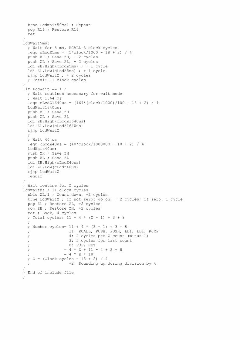
; Wait routines;; Wait 50 ms; When the clock frequency is above 3.1 MHz the maximum; that can be counted in 16 bits. Therefore the 5 ms routine; is called for 10 timesLcdWait50ms: push R16 ; Save R16 ldi R16,10 ; 10 times 5 ms rcall LcdWait5ms dec R16 brne LcdWait50ms1 pop R16 ret;LcdWait5ms: ; Wait 5 ms .equ cLcdZ5ms = (5*clock/1000 - 10 + 2) / 4 ldi ZH,High(cLcdZ5ms) ldi ZL,Low(cLcdZ5ms)

rjmp LcdWaitZ;.if LcdWait == 1 ; Wait mode delays ; Wait 1.6 ms .equ cLcdZ1600us = (1600*clock/1000000 - 10 + 2) / 4 LcdWait1600us: ldi ZH,High(cLcdZ1600us) ldi ZL,Low(cLcdZ1600us) rjmp LcdWaitZ ; ; Wait 40 us LcdWait40: ldi ZH,High(cLcdZ40us) ldi ZL,Low(cLcdZ40us) rjmp LcdWaitZ .endif;; Wait routine with Z cyclesLcdWaitZ: sbiw ZL,1 ; Count down, 2 clock cycles brne LcdWaitZ ; Not zero: 2 clock cycles, Zero: 1 clock cycle ret ; Back, 4 clock cycles; ; clock cycles = 7 * 4 + (Z - 1) + 3 + 4 ; 7: RCALL, LDI, LDI, RJMP ; 4: 4 clock cycles per count - 1 ; 3: 3 clock cycles for last count ; 4: RET ; = 4 * Z + 7 - 4 + 3 + 4 ; = 4 * Z + 10 ; Z = (clock cycles - 10 + 2) / 4 ; +2: Rounding prior to division by 4
A possible variation is to save register pair ZH:ZL prior to using it in the tworesp. four wait routines and to restore it on the end of LcdWaitZ:. The fourpushes and pops only change the calculation of Z slightly.
The derivation of Z fromthe clock frequency leadsto exact delays indepen-dant from clock. Thesimulated times (withavr_sim are for com-pletely different clockrates for 5 ms.
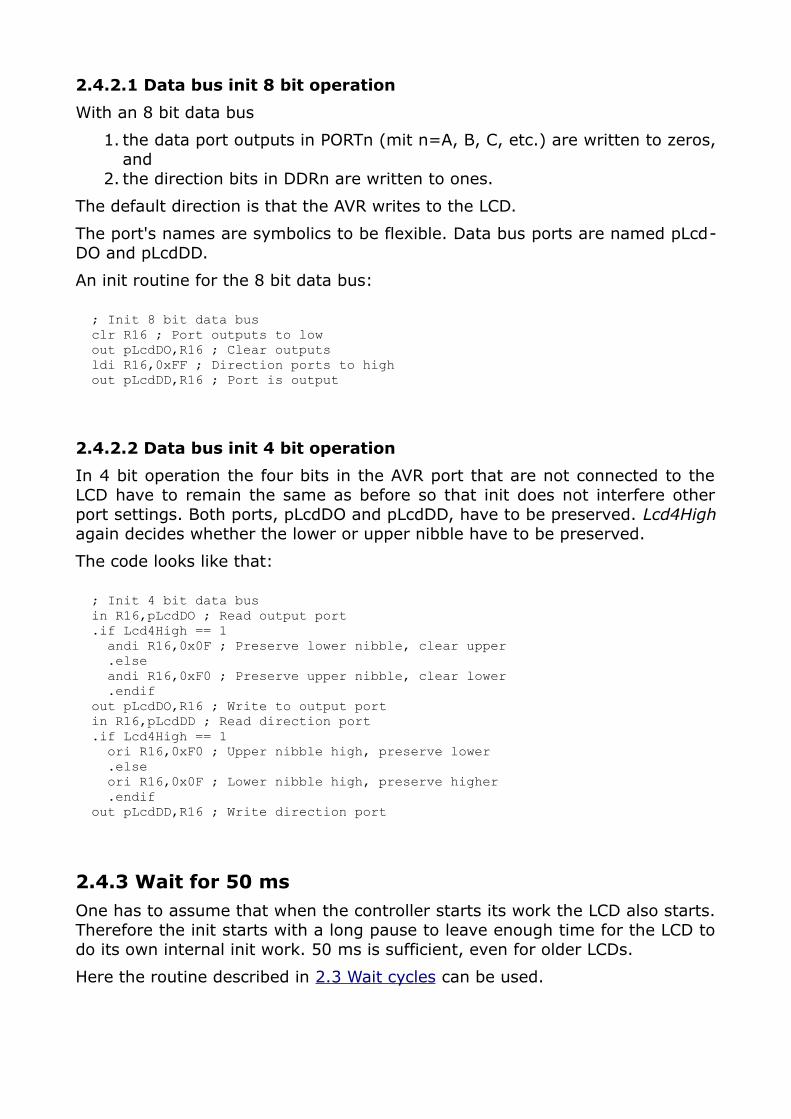
2.4 Initing the LCDCommunication with the LCD starts with the configuration of the control pins(A) and the 2.4.2 data bus (B). Then the 50 ms wait cycle is performed (C) fol-lowed by switching the LCD to 8 bit mode (D), no matter which data bus willbe used later on.
2.4.1 Control pinsTo be configured are
1. the E pin, 2. the RS pin, 3. and, if reading the busy flag is de-
sired, the RW pin.
To be able to have those three pins locat-ed in different I/O ports (whereever thereis a bit available), those I/O ports andpins are named with symbols to achieve amaximum of flexibility and understand-a-bility:
• pLcdCEO Output port E pin, • pLcdCRSO Output port RS pin, • pLcdCRWO Output port RW pin (if
in busy mode), • pLcdCED Direction port E pin, • pLcdCRSD Direction port RS pin, • pLcdCRWD Direction port RW pin
(if busy).
The names consist of
1. p for all port symbols, 2. Lcd those connected with the LCD, 3. C for control pins, 4. E, RS or RW for the three control
pins, and 5. O for Output or D for direction
ports.
To be consistent also the portpins get symbolic names. Those start with b forportbit and relate to the output bits PORTnb (eg. .equ bLcdCEO = PORTB2) orthe direction bits DDnb, eg. .equ bLcdCED = DDB2.
The init routine for the control pins therefore looks like that:
; Init Control pins cbi pLcdCEO,bLcdCEO ; E output low sbi pLcdCED,bLcdCED ; E direction high cbi pLcdCRSO,bLcdCRSO ; RS output low sbi pLcdCRSD,bLcdCRSD ; RS direction high .ifdef bLcdCRWO ; If RW pin defined cbi pLcdCRWO,bLcdCRWO ; RW output low sbi pLcdCRWD,bLcdCRWD ; RW direction high .endif
2.4.2 Data bus initInit of the data bus is slightly different under an 2.4.2.1 8 bit data bus and fora 2.4.2.2 4 bit data bus.
2.4.2.1 Data bus init 8 bit operation
With an 8 bit data bus
1. the data port outputs in PORTn (mit n=A, B, C, etc.) are written to zeros,and
2. the direction bits in DDRn are written to ones.
The default direction is that the AVR writes to the LCD.
The port's names are symbolics to be flexible. Data bus ports are named pLcd-DO and pLcdDD.
An init routine for the 8 bit data bus:
; Init 8 bit data bus clr R16 ; Port outputs to low out pLcdDO,R16 ; Clear outputs ldi R16,0xFF ; Direction ports to high out pLcdDD,R16 ; Port is output
2.4.2.2 Data bus init 4 bit operation
In 4 bit operation the four bits in the AVR port that are not connected to theLCD have to remain the same as before so that init does not interfere otherport settings. Both ports, pLcdDO and pLcdDD, have to be preserved. Lcd4Highagain decides whether the lower or upper nibble have to be preserved.
The code looks like that:
; Init 4 bit data bus in R16,pLcdDO ; Read output port .if Lcd4High == 1 andi R16,0x0F ; Preserve lower nibble, clear upper .else andi R16,0xF0 ; Preserve upper nibble, clear lower .endif out pLcdDO,R16 ; Write to output port in R16,pLcdDD ; Read direction port .if Lcd4High == 1 ori R16,0xF0 ; Upper nibble high, preserve lower .else ori R16,0x0F ; Lower nibble high, preserve higher .endif out pLcdDD,R16 ; Write direction port
2.4.3 Wait for 50 msOne has to assume that when the controller starts its work the LCD also starts.Therefore the init starts with a long pause to leave enough time for the LCD todo its own internal init work. 50 ms is sufficient, even for older LCDs.
Here the routine described in 2.3 Wait cycles can be used.

2.4.4 Switching the LCD to 8 bit operationAll LCDs, even when they are supposed to operate in 4 bit mode, have to beswitched to 8 bit mode first. This ensures that from whatever state the LCDoperates in a predictable mode and later switchung to 4 bit is a reliable se-quence.
To switch to 8 bit mode is done by
1. clearing the RS pin (and RW pin, if necessary), 2. placing 0x30 on the data bus (in 4 bit mode: 0x3 on the data bus
nibble), 3. activating the E pin for one microsecond and then low again, and by 4. waiting for 1.6 ms.
If this procedure is repeated two or three times, we are absolutely sure thatthe LCD is in 8 bit mode.
The code in 8 bit mode:
; Switching to 8 bit mode cbi pLcdCRSO,bLcdCRSO ; RS pin Low ldi R16,0x30 ; 8 bit mode out pLcdDO,R16 ; to data bus rcall LcdPulseE ; E pin high for one us rcall LcdWait1600us ; Wait 1.6 ms
The last two instructions shall be repeated two or three times.
With a 4 bit data bus the code looks as follows:
; Switching to 8 bit operation with a 4 bit data bus cbi pLcdCRSO,bLcdCRSO ; RS pin Low in R16,pLcdDO ; Read output port .if Lcd4High == 1 andi R16,0x0F ; Clear uppoer nibble, preserve lower ori R16,0x30 ; Upper nibble to 0x3 .else andi R16,0xF0 ; Clear lower nibble, preserve upper ori R16,0x03 ; Lower nibble to 0x3 .endif out pLcdDO,R16 ; to data bus rcall LcdPulseE ; Activate E pin for one us rcall LcdWait1600us ; Wait 1.6 ms
2.4.5 Switching the LCD from 8 bit to 4 bit operationThis part is only performed if the LCD shall beoperated in 4 bit mode.
The code above is repeated but ori R16,0x30 andori R16,0x03 is replaced by 0x20 resp. 0x02. Andmake sure that the command is sent only once.From now on each write and read operation re-quires two pulses on the E pin: first the upper
and second the lower nibble are wrote or read.
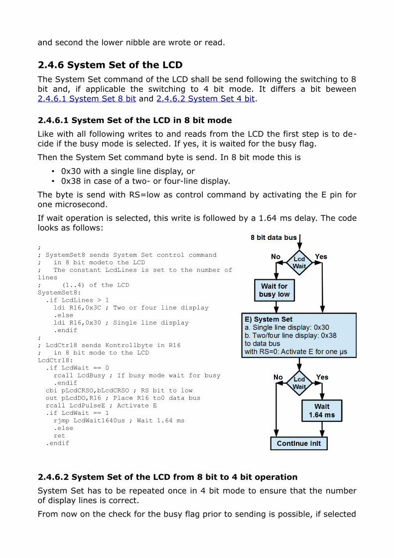
2.4.6 System Set of the LCDThe System Set command of the LCD shall be send following the switching to 8bit and, if applicable the switching to 4 bit mode. It differs a bit beween2.4.6.1 System Set 8 bit and 2.4.6.2 System Set 4 bit.
2.4.6.1 System Set of the LCD in 8 bit mode
Like with all following writes to and reads from the LCD the first step is to de-cide if the busy mode is selected. If yes, it is waited for the busy flag.
Then the System Set command byte is send. In 8 bit mode this is
• 0x30 with a single line display, or • 0x38 in case of a two- or four-line display.
The byte is send with RS=low as control command by activating the E pin forone microsecond.
If wait operation is selected, this write is followed by a 1.64 ms delay. The codelooks as follows:
;; SystemSet8 sends System Set control command; in 8 bit modeto the LCD; The constant LcdLines is set to the number oflines; (1..4) of the LCDSystemSet8: .if LcdLines > 1 ldi R16,0x3C ; Two or four line display .else ldi R16,0x30 ; Single line display .endif;; LcdCtrl8 sends Kontrollbyte in R16; in 8 bit mode to the LCDLcdCtrl8: .if LcdWait == 0 rcall LcdBusy ; If busy mode wait for busy .endif cbi pLcdCRSO,bLcdCRSO ; RS bit to low out pLcdDO,R16 ; Place R16 to0 data bus rcall LcdPulseE ; Activate E .if LcdWait == 1 rjmp LcdWait1640us ; Wait 1.64 ms .else ret .endif
2.4.6.2 System Set of the LCD from 8 bit to 4 bit operation
System Set has to be repeated once in 4 bit mode to ensure that the numberof display lines is correct.
From now on the check for the busy flag prior to sending is possible, if selected
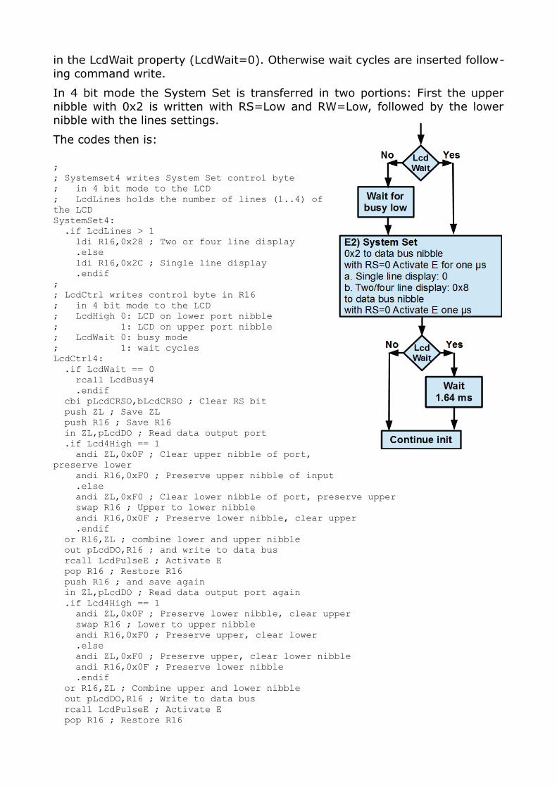
in the LcdWait property (LcdWait=0). Otherwise wait cycles are inserted follow-ing command write.
In 4 bit mode the System Set is transferred in two portions: First the uppernibble with 0x2 is written with RS=Low and RW=Low, followed by the lowernibble with the lines settings.
The codes then is:
;; Systemset4 writes System Set control byte; in 4 bit mode to the LCD; LcdLines holds the number of lines (1..4) ofthe LCDSystemSet4: .if LcdLines > 1 ldi R16,0x28 ; Two or four line display .else ldi R16,0x2C ; Single line display .endif;; LcdCtrl writes control byte in R16; in 4 bit mode to the LCD; LcdHigh 0: LCD on lower port nibble; 1: LCD on upper port nibble; LcdWait 0: busy mode; 1: wait cyclesLcdCtrl4: .if LcdWait == 0 rcall LcdBusy4 .endif cbi pLcdCRSO,bLcdCRSO ; Clear RS bit push ZL ; Save ZL push R16 ; Save R16 in ZL,pLcdDO ; Read data output port .if Lcd4High == 1 andi ZL,0x0F ; Clear upper nibble of port,preserve lower andi R16,0xF0 ; Preserve upper nibble of input .else andi ZL,0xF0 ; Clear lower nibble of port, preserve upper swap R16 ; Upper to lower nibble andi R16,0x0F ; Preserve lower nibble, clear upper .endif or R16,ZL ; combine lower and upper nibble out pLcdDO,R16 ; and write to data bus rcall LcdPulseE ; Activate E pop R16 ; Restore R16 push R16 ; and save again in ZL,pLcdDO ; Read data output port again .if Lcd4High == 1 andi ZL,0x0F ; Preserve lower nibble, clear upper swap R16 ; Lower to upper nibble andi R16,0xF0 ; Preserve upper, clear lower .else andi ZL,0xF0 ; Preserve upper, clear lower nibble andi R16,0x0F ; Preserve lower nibble .endif or R16,ZL ; Combine upper and lower nibble out pLcdDO,R16 ; Write to data bus rcall LcdPulseE ; Activate E pop R16 ; Restore R16

pop ZL ; Restore ZL .if LcdWait == 1 rjmp LcdWait1640us ; Wait 1.64 ms .else ret .endif
2.4.7 Finalize initFollowing System Set further properties ofthe LED can be configured.
The Entry mode shall be modified. Cursormove direction is by default right to left (Ja-panese) and should be set to left to right byissuing 0x06 as command.
The cursor behaviour can be set to display anunderscore for it and to blink the characterat the cursor.
If after init the display shows any wild char-acters those can be deleted by clearing thedisplay. If in wait mode, this should be fol-lowed by a pause of 1.6 ms.
With this the LCD is completely inited and wecan start working with the LCD and we candisplay characters. The code for displayingcharacters is:
; Display character A ldi R16,'A' ; Load ASCII character A to R16;; LcdChar displays character in R16 on the display; LcdWait determines if wait cycles are used (=1) or; if busy is read (=0); LcdBits determines if a 4 or 8 bit data bus is used; Lcd4High determines, in case of a 4 bit bus, if the; data port is connected to the upper (=1) or lower; (=0) nibble of the AVR portLcdChar: .if LcdWait == 0 rcall LcdBusy ; Wait for busy clear .endif sbi pLcdCRSO,bLcdCRSO ; RS pin high .if LcdBits == 8 out pLcdDD,R16 ; To data bus .else push ZL ; Save ZL push R16 ; Save R16 in ZL,pLcdDO ; Read output port .if Lcd4High == 1 andi ZL,0x0F ; Clear upper nibble, preserve lower andi R16,0xF0 ; Clear lower nibble .else andi ZL,0xF0 ; Clear lower nibble, preserve higher swap R16 ; Upper to lower nibble andi R16,0x0F ; Clear upper nibble .endif
or R16,ZL ; combine out pLcdDO,R16 ; Write to data bus rcall LcdPulseE ; Activate E pop R16 ; Restore R16 in ZL,pLcdDO ; Read output port again andi R16,0x0F ; Clear upper nibble .if Lcd4High == 1 andi ZL,0x0F ; Clear upper nibble swap R16 ; Lower to upper nibble .else andi ZL,0xF0 ; Clear lower nibble .endif or R16,ZL ; Combine nibbles out pLcdDD,R16 ; To data bus pop ZL ; Restore ZL .endif rcall LcdPulseE ; Activate E .if LcdWait == 1 rjmp LcdWait40us ; Wait 40 us .else ret .endif
That sounds a little bit complicated but works in all cases. Conditional assem-bly is used to tailor the software to the specific case: code is solely generated ifreally needed.
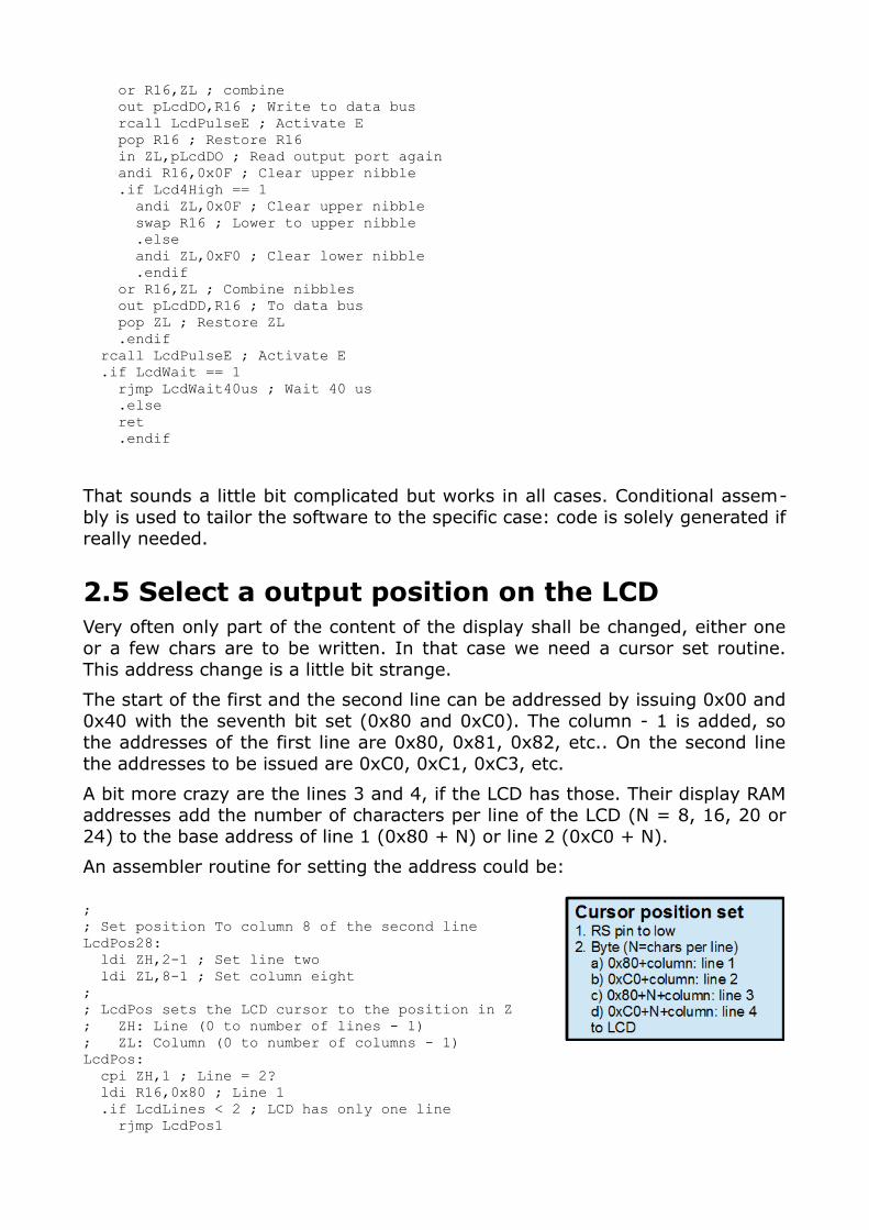
2.5 Select a output position on the LCDVery often only part of the content of the display shall be changed, either oneor a few chars are to be written. In that case we need a cursor set routine.This address change is a little bit strange.
The start of the first and the second line can be addressed by issuing 0x00 and0x40 with the seventh bit set (0x80 and 0xC0). The column - 1 is added, sothe addresses of the first line are 0x80, 0x81, 0x82, etc.. On the second linethe addresses to be issued are 0xC0, 0xC1, 0xC3, etc.
A bit more crazy are the lines 3 and 4, if the LCD has those. Their display RAMaddresses add the number of characters per line of the LCD (N = 8, 16, 20 or24) to the base address of line 1 (0x80 + N) or line 2 (0xC0 + N).
An assembler routine for setting the address could be:
;; Set position To column 8 of the second lineLcdPos28: ldi ZH,2-1 ; Set line two ldi ZL,8-1 ; Set column eight;; LcdPos sets the LCD cursor to the position in Z; ZH: Line (0 to number of lines - 1); ZL: Column (0 to number of columns - 1)LcdPos: cpi ZH,1 ; Line = 2? ldi R16,0x80 ; Line 1 .if LcdLines < 2 ; LCD has only one line rjmp LcdPos1

.endif brcs LcdPos1 ; No, line 1 ldi R16,0xC0 ; Line 2 address .if LcdLines == 2 ; LCD has only two lines rjmp LcdPos1 .endif breq LcdPos1 ldi R16,0x80+LcdCols ; Line 3 address cpi ZH,2 ; Line = 3 breq LcdPos1 ldi R16,0xC0+LcdCols ; Line 4 addressLcdPos1: add R16,ZL ; Add column rjmp LcdCtrl ; Write control command to LCD
2.6 To generate own charactersIn each LCD the first eight charac-ters (char 0x00 to 0x07) can bealtered by the user and can beused to display own characters.
The character generator RAM ofthe first eight characters are ad-dressed as follows:
1. The address has six bits: • the upper three bits
address the number ofthe character,
• the three lower bitsaddress the lines ofthe character, from topdown.
When writing the addressthe two bits 0b01 are added on the left and send with RS=low to theLCD.
2. The data to be written to those addresses has five bits. Ones turn thepixel on, zeros off (to background color). The five bits have to be writtenwith preceeding 0b000 with RS=high to the LCD. If the cursor directionI/D during init was set to Increase, the eight bytes data can be send in arow, without re-writing the address (Auto-Increment).
To send those special chars, those would be best written to a table. The tableshall consist of one address byte and eight data bytes. To come to an evennumber of bytes per row, a dummy character is added (that is ignored by thesoftware) to avoid insertion of a null byte by the assembler.
Address DummyLines
1 2 3 4 5 6 7 8
Byte 0 Byte Byte Byte Byte Byte Byte Byte Byte
Byte 0 Byte Byte Byte Byte Byte Byte Byte Byte
... further characters ...
Byte 0 Byte Byte Byte Byte Byte Byte Byte Byte
0 0 (End of table)
To generate such tables a spreadsheet application can be used. Here suchspreadsheets are described. The generated assembler table can be copied andpasted to the source code file.
The following code writes the table content to the LCD:
;; LcdSpec generates special characters to the LCD; Z points to 2*Table address; Tabellenformat:; 1.Byte: Address of character 0b01zzz000,; 0: End of table; 2.Byte: Dummy; 3. to 10.Byte: Data of the lines 1 to 8LcdSpec: push R0 ; R0 is counterLcdSpec1: lpm R16,Z+ ; Read address of characters tst R16 ; End of the table? breq LcdSpec3 ; End of table rcall LcdCtrl ; Write address adiw ZL,1 ; Overread dummy ldi R16,8 ; 8 byte data per character mov R0,R16 ; R0 is counterLcdSpec2: lpm R16,Z+ ; Read data byte rcall LcdData ; Write data byte dec R0 ; Count down brne LcdSpec2 ; Go on with data rjmp LcdSpec1 ; Next characterLcdSpec3: pop R0 ; Restore R0 ldi ZH,0 ; Cursor home ldi ZL,0 rjmp LcdPos;
The following table generates arrow characters on the LCD.
;; Table of character codesCharCodes:.db 64,0,0,12,6,31,6,12,0,0 ; Z = 0, arrow right.db 72,0,0,6,12,31,12,6,0,0 ; Z = 1, arrow left.db 80,0,4,14,31,21,4,4,4,0 ; Z = 2, arrow up.db 88,0,4,4,4,21,31,14,4,0 ; Z = 3, arrow down.db 96,0,0,15,3,5,9,16,0,0 ; Z = 4, arrow rigth up
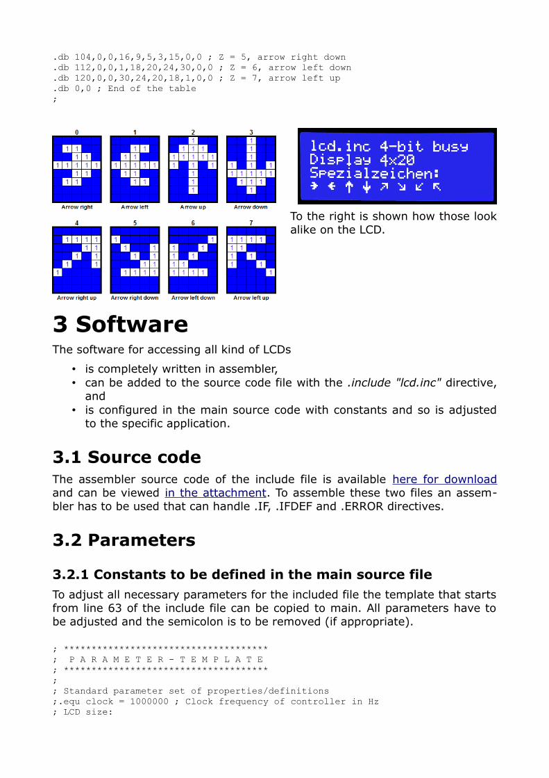
.db 104,0,0,16,9,5,3,15,0,0 ; Z = 5, arrow right down
.db 112,0,0,1,18,20,24,30,0,0 ; Z = 6, arrow left down
.db 120,0,0,30,24,20,18,1,0,0 ; Z = 7, arrow left up
.db 0,0 ; End of the table;
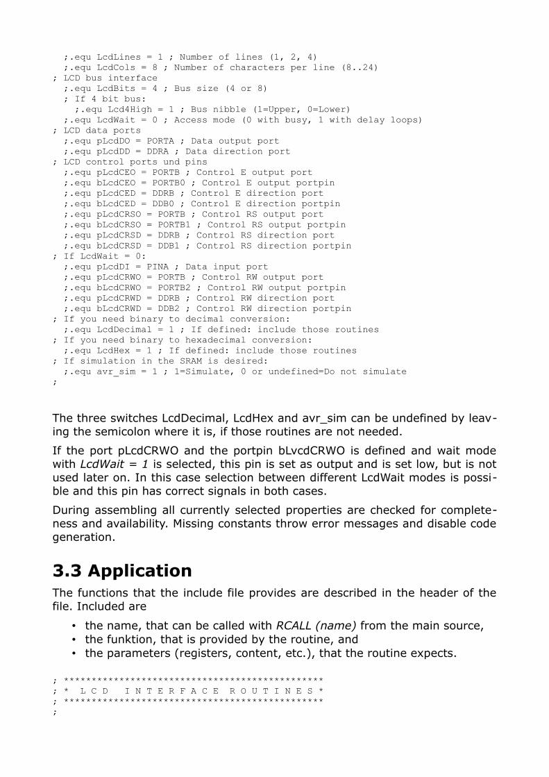
To the right is shown how those lookalike on the LCD.
3 SoftwareThe software for accessing all kind of LCDs
• is completely written in assembler, • can be added to the source code file with the .include "lcd.inc" directive,
and • is configured in the main source code with constants and so is adjusted
to the specific application.
3.1 Source codeThe assembler source code of the include file is available here for downloadand can be viewed in the attachment. To assemble these two files an assem-bler has to be used that can handle .IF, .IFDEF and .ERROR directives.
3.2 Parameters
3.2.1 Constants to be defined in the main source fileTo adjust all necessary parameters for the included file the template that startsfrom line 63 of the include file can be copied to main. All parameters have tobe adjusted and the semicolon is to be removed (if appropriate).
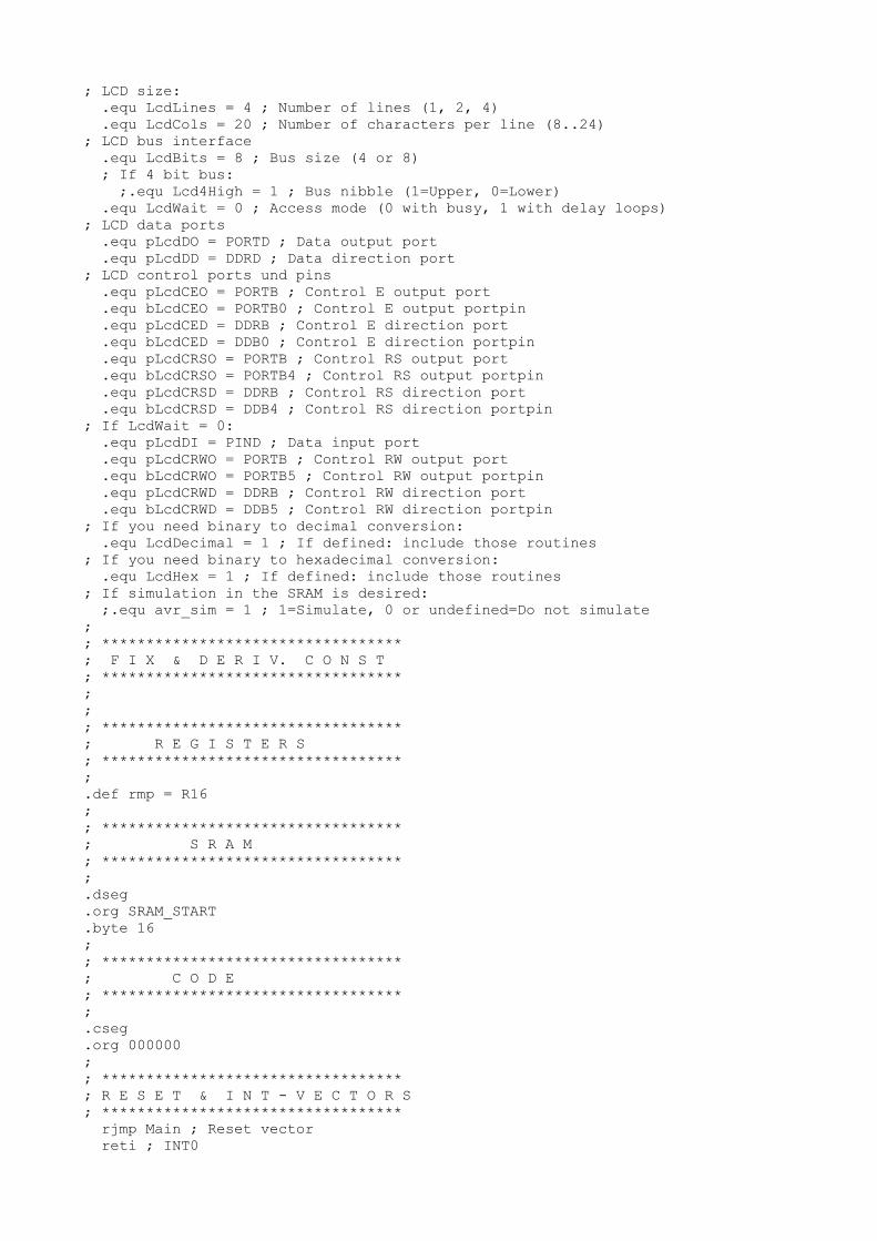
; *************************************; P A R A M E T E R - T E M P L A T E; *************************************;; Standard parameter set of properties/definitions;.equ clock = 1000000 ; Clock frequency of controller in Hz; LCD size:
;.equ LcdLines = 1 ; Number of lines (1, 2, 4) ;.equ LcdCols = 8 ; Number of characters per line (8..24); LCD bus interface ;.equ LcdBits = 4 ; Bus size (4 or 8) ; If 4 bit bus: ;.equ Lcd4High = 1 ; Bus nibble (1=Upper, 0=Lower) ;.equ LcdWait = 0 ; Access mode (0 with busy, 1 with delay loops); LCD data ports ;.equ pLcdDO = PORTA ; Data output port ;.equ pLcdDD = DDRA ; Data direction port; LCD control ports und pins ;.equ pLcdCEO = PORTB ; Control E output port ;.equ bLcdCEO = PORTB0 ; Control E output portpin ;.equ pLcdCED = DDRB ; Control E direction port ;.equ bLcdCED = DDB0 ; Control E direction portpin ;.equ pLcdCRSO = PORTB ; Control RS output port ;.equ bLcdCRSO = PORTB1 ; Control RS output portpin ;.equ pLcdCRSD = DDRB ; Control RS direction port ;.equ bLcdCRSD = DDB1 ; Control RS direction portpin; If LcdWait = 0: ;.equ pLcdDI = PINA ; Data input port ;.equ pLcdCRWO = PORTB ; Control RW output port ;.equ bLcdCRWO = PORTB2 ; Control RW output portpin ;.equ pLcdCRWD = DDRB ; Control RW direction port ;.equ bLcdCRWD = DDB2 ; Control RW direction portpin; If you need binary to decimal conversion: ;.equ LcdDecimal = 1 ; If defined: include those routines; If you need binary to hexadecimal conversion: ;.equ LcdHex = 1 ; If defined: include those routines; If simulation in the SRAM is desired: ;.equ avr_sim = 1 ; 1=Simulate, 0 or undefined=Do not simulate;
The three switches LcdDecimal, LcdHex and avr_sim can be undefined by leav-ing the semicolon where it is, if those routines are not needed.
If the port pLcdCRWO and the portpin bLvcdCRWO is defined and wait modewith LcdWait = 1 is selected, this pin is set as output and is set low, but is notused later on. In this case selection between different LcdWait modes is possi-ble and this pin has correct signals in both cases.
During assembling all currently selected properties are checked for complete-ness and availability. Missing constants throw error messages and disable codegeneration.
3.3 ApplicationThe functions that the include file provides are described in the header of thefile. Included are
• the name, that can be called with RCALL (name) from the main source, • the funktion, that is provided by the routine, and • the parameters (registers, content, etc.), that the routine expects.
; ***********************************************; * L C D I N T E R F A C E R O U T I N E S *; ***********************************************;
; +-------+----------------+--------------+; |Routine|Function |Parameters |; +-------+----------------+--------------+; |LcdInit|Inits the LCD |Ports, pins |; | |in the desired | |; | |mode | |; +-------+----------------+--------------+; |LcdText|Displays the |Z=2*Table |; | |text in flash | address |; | |memory starting |0x0D: Next |; | |with line 1 | line |; | | |0xFF: Ignore |; | | |0xFE: Text end|; +-------+----------------+--------------+; |LcdSram|Display the text|Z=SRAM-Address|; | |in SRAM |R16: number of|; | | | characters|; +-------+----------------+--------------+; |LcdChar|Display charac- |R16: Character|; | |ter on LCD | |; +-------+----------------+--------------+; |LcdCtrl|Output control |R16: Control |; | |byte to LCD | byte |; +-------+----------------+--------------+; |LcdPos |Set position on |ZH: Line 0123 |; | |the LCD |ZL: Col 0.. |; +-------+----------------+--------------+; |LcdSpec|Generate special|Z: 2*Table |; | |characters | address |; +-------+----------------+--------------+; | S W I T C H L C D D E C I M A L |; +-------+----------------+--------------+; |LcdDec2|Convert to two |R16: Binary |; | |decimal digits | 8 bit |; +-------+----------------+--------------+; |LcdDec3|Convert to three|R16: Binary |; | |decimal digits, | 8 bit |; | |supp. leading 0s| |; +-------+----------------+--------------+; |LcdDec5|Convert to five |Z: Binary |; | |decimal digits, | 16 bit |; | |supp. leading 0s| |; +-------+----------------+--------------+; | S W I T C H L C D H E X |; +-------+----------------+--------------+; |LcdHex2|Convert to two |R16: Binary |; | |digits in hex | 8 bit |; +-------+----------------+--------------+; |LcdHex4|Convert to four |Z: Binary |; | |digits in hex | 16 bit |; +-------+----------------+--------------+
The routines are programmed in a way that the registers ZH and ZL as well asR2, R1 and R0 are used. R2, R1 and R0 are preserved (restoring their contentafter use). ZH and ZL are not always preserved. R16 is also used and is not al-ways preserved. Consult the source code if in doubt.
3.3.1 Init the LCDWith rcall LcdInit the LCD is inited. This routine is called once during init of thehardware. The routine
1. configures the control- and data bus-output pins according to the givenport and portbit information,
2. waits 50 ms, until the LCD has done its self-initiation, 3. switches the LCD four times to 8 bit mode, 4. switches, if selected, to 4 bit mode, 5. performs the Function Set (mode and line selection), 6. switches the LCD on and the cursor and cursor blink off, and 7. clears the LCD.
3.3.2 Display text on the LCDWith rcall LcdInit the LCD can be fed with predefined text from a table in flashmemory. The table
• address has to be set, with its doubled value, to the register pair Z, • should consist of .db directives and should have an even number of bytes
per line, if not: add a 0xFF that is ignored in the text output routine, • does not need to write complete lines (unless you want to override previ-
ous content) but can be, with a 0x0D byte, moved to the beginning ofthe next line (if the LCD has multiple lines),
• ends with 0xFE.
3.3.3 Displaying text from the SRAM on the LCDWith rcall LcdSram the text in SRAM, to which register pair Z points, is dis-played on the LCD. The number of characters to be displayed is in R16.
3.3.4 To display a single character on the LCDrcall LcdChar outputs the character in R16 on the current position of the LCD.
3.3.5 To send a control command to the LCDrcall LcdCtrl sends the byte in R16 as control command to the LCD.
3.3.6 To adjust the cursor position of the LCDrcall LcdPos adjusts the cursor position of the LCD to the line given in ZH(0...LcdLines-1) and the column given in ZL (0...LcdCols-1).
3.3.7 Generate special characters in the LCDBy rcall LcdSpec a table with special chars is send to the LCD The table con-sists of
1. one address byte (0b01zz.z000), in which z is the character number(0...7),
2. one dummy byte (e.g. 0), plus
3. eight data bytes, that hold the five bits from right to left per characterline, from to below,
4. a null byte as address byte, that ends output.
The special chars can be inserted with 0x00 to 0x07 in text output, e.g. .db"Special char 0 =",0x00,0xFF.
3.3.8 Display binaries as decimal on LCDThose routines are included in the code and can be called with rcall LcdDec2,rcall LcdDec3 and rcall LcdDec5 if the switch LcdDecimal is defined in thesource code of the main program.
LcdDec2 displays the binary in R16 with two decimal digits. If R16 is largerthan 99 the 99 is displayed. A leading zero is not blanked.
LcdDec3 displays an 8 bit binary in R16 with three digits. Leading zeros areblanked.
LcdDec5 displays the 16 bit binary in Z (ZH:ZL) with five digits at the currentdisplay position. Leading zeros are blanked.
3.3.9 Display binaries hexadecimal on the LCDThose routines are included in the code if the switch LcdHex is defined in thesource code.
LcdHex2 displays the 8 bit binary in R16 with two digits in in hexadecimalform. LcdHex4 displays the 16 bit binary in Z in hexadecimal form.
3.4 Size of the program of the assembled versionsThe size of the assembled program code depends from the chosen parameters.The table displays those sizes, solely resulting from the include file.
VersionSize
wordsAccumulated
Minimal version (1 MHz, 8 bit, wait mode, w/o dec/hex)
138 -
Wait ==> Busy +9 147
1 MHz ==> 20 MHz +20 158
8 bit ==> 4 bit +44 182
LcdDecimal +86 224
LcdHex +14 152
Maximum version(20 MHz, 4-Bit, busy mode,Decimal- and Hex-Conversion)
+197 335
The include file is optimized by conditional assembling. The size is minimized
and tailored to the application. No unnecessary code blows the code up, as isthe case with C or Basic compilers.
3.5 Example programsThe use of the include software for the LCD is demonstrated with two exampleprograms:
1. with an 8 bit data bus and displaying decimal and hexadecimal numbers,and
2. with a 4 bit data bus with generation and display of eight special charac-ters.
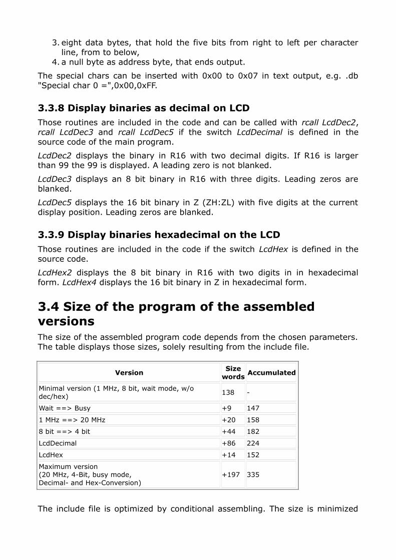
3.5.1 Example program 8 bitThe example program (in assemblersource code format here, in theattachment) demonstrates, with anATmega8, the 8 bit connection and theoutput of decimal and hexadecimalnumbers on the LCD and including theder include file lcd.inc into the source code. In this case the ATmega8 operateswith an 8 MHz crystal.
The routine LcdInit initializes the LCD, with LcdText the display mask is issuedas listed in the table InitText:. LcdPos positions the LCD cursor to the lines 3and 4 and LcdDec5 display the 16 bit binary in decimal, LcdHex4 in hexadeci-mal form.
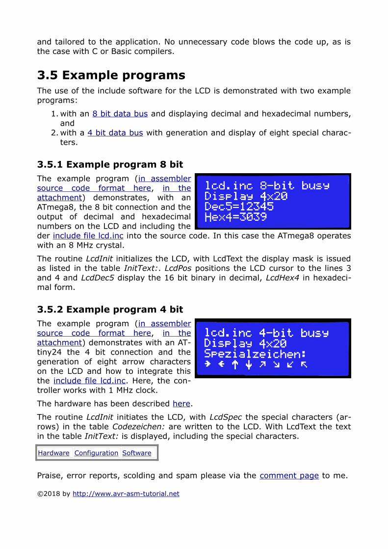
3.5.2 Example program 4 bitThe example program (in assemblersource code format here, in theattachment) demonstrates with an AT-tiny24 the 4 bit connection and thegeneration of eight arrow characterson the LCD and how to integrate thisthe include file lcd.inc. Here, the con-troller works with 1 MHz clock.
The hardware has been described here.
The routine LcdInit initiates the LCD, with LcdSpec the special characters (ar-rows) in the table Codezeichen: are written to the LCD. With LcdText the textin the table InitText: is displayed, including the special characters.
Hardware Configuration Software
Praise, error reports, scolding and spam please via the comment page to me.
©2018 by http://www.avr-asm-tutorial.net
Path: Home => AVR-EN => Applications => LCD on an AVR => include fileAVR applications
LCD control withan AVR inassembler
Include file "lcd.inc"
Include file for accessing an LCD with an AVRThe assembler source code, as shown here, can be downloaded here in sourceformat.
;; *********************************; * LCD include routines *; * (C)2018 avr-asm-tutorial.net *; *********************************;; ***********************************************; * L C D I N T E R F A C E R O U T I N E S *; ***********************************************;; +-------+----------------+--------------+; |Routine|Function |Parameters |; +-------+----------------+--------------+; |LcdInit|Inits the LCD |Ports, pins |; | |in the desired | |; | |mode | |; +-------+----------------+--------------+; |LcdText|Displays the |Z=2*Table |; | |text in flash | address |; | |memory starting |0x0D: Next |; | |with line 1 | line |; | | |0xFF: Ignore |; | | |0xFE: Text end|; +-------+----------------+--------------+; |LcdSram|Display the text|Z=SRAM-Address|; | |in SRAM |R16: number of|; | | | characters|; +-------+----------------+--------------+; |LcdChar|Display charac- |R16: Character|; | |ter on LCD | |; +-------+----------------+--------------+; |LcdCtrl|Output control |R16: Control |; | |byte to LCD | byte |; +-------+----------------+--------------+; |LcdPos |Set position on |ZH: Line 0123 |; | |the LCD |ZL: Col 0.. |; +-------+----------------+--------------+; |LcdSpec|Generate special|Z: 2*Table |; | |characters | address |; +-------+----------------+--------------+; | S W I T C H L C D D E C I M A L |

; +-------+----------------+--------------+; |LcdDec2|Convert to two |R16: Binary |; | |decimal digits | 8 bit |; +-------+----------------+--------------+; |LcdDec3|Convert to three|R16: Binary |; | |decimal digits, | 8 bit |; | |supp. leading 0s| |; +-------+----------------+--------------+; |LcdDec5|Convert to five |Z: Binary |; | |decimal digits, | 16 bit |; | |supp. leading 0s| |; +-------+----------------+--------------+; | S W I T C H L C D H E X |; +-------+----------------+--------------+; |LcdHex2|Convert to two |R16: Binary |; | |digits in hex | 8 bit |; +-------+----------------+--------------+; |LcdHex4|Convert to four |Z: Binary |; | |digits in hex | 16 bit |; +-------+----------------+--------------+;; *************************************; P A R A M E T E R - T E M P L A T E; *************************************;; (Copy to your source code, remove ; and adjust; parameters to fit your hardware);; Standard parameter set of properties/definitions;.equ clock = 1000000 ; Clock frequency of controller in Hz; LCD size: ;.equ LcdLines = 1 ; Number of lines (1, 2, 4) ;.equ LcdCols = 8 ; Number of characters per line (8..24); LCD bus interface ;.equ LcdBits = 4 ; Bus size (4 or 8) ; If 4 bit bus: ;.equ Lcd4High = 1 ; Bus nibble (1=Upper, 0=Lower) ;.equ LcdWait = 0 ; Access mode (0 with busy, 1 with delay loops); LCD data ports ;.equ pLcdDO = PORTA ; Data output port ;.equ pLcdDD = DDRA ; Data direction port; LCD control ports und pins ;.equ pLcdCEO = PORTB ; Control E output port ;.equ bLcdCEO = PORTB0 ; Control E output portpin ;.equ pLcdCED = DDRB ; Control E direction port ;.equ bLcdCED = DDB0 ; Control E direction portpin ;.equ pLcdCRSO = PORTB ; Control RS output port ;.equ bLcdCRSO = PORTB1 ; Control RS output portpin ;.equ pLcdCRSD = DDRB ; Control RS direction port ;.equ bLcdCRSD = DDB1 ; Control RS direction portpin; If LcdWait = 0: ;.equ pLcdDI = PINA ; Data input port ;.equ pLcdCRWO = PORTB ; Control RW output port ;.equ bLcdCRWO = PORTB2 ; Control RW output portpin ;.equ pLcdCRWD = DDRB ; Control RW direction port ;.equ bLcdCRWD = DDB2 ; Control RW direction portpin; If you need binary to decimal conversion: ;.equ LcdDecimal = 1 ; If defined: include those routines; If you need binary to hexadecimal conversion: ;.equ LcdHex = 1 ; If defined: include those routines; If simulation in the SRAM is desired: ;.equ avr_sim = 1 ; 1=Simulate, 0 or undefined=Do not simulate;; *****************************************
; T E X T T E M P L A T E S; *****************************************;; Tables to copy for diverse sizes;; --------------------------; Single line LCD; 8 chars per line; Text_1_8:; .db " ",0xFE,0xFF; 01234567;; 16 chars per line; Text_1_16:; .db " ",0xFE,0xFF; 0123456789012345;; 20 chars per line; Text_1_20:; .db " ",0xFE,0xFF; 01234567890123456789;; 24 chars per line; Text_1_24:; .db " ",0xFE,0xFF; 012345678901234567890123;; --------------------------; Two line LCD; 16 chars per line; Text_2_16:; .db " ",0x0D,0xFF; .db " ",0xFE,0xFF; 0123456789012345;; 20 chars per line; Text_2_20:; .db " ",0x0D,0xFF; .db " ",0xFE,0xFF; 01234567890123456789;; 24 chars per line; Text_2_24:; .db " ",0x0D,0xFF; .db " ",0xFE,0xFF; 012345678901234567890123;; --------------------------; Four line LCD; 16 chars per line; Text_4_16:; .db " ",0x0D,0xFF; .db " ",0x0D,0xFF; .db " ",0x0D,0xFF; .db " ",0xFE,0xFF; 0123456789012345;; 20 chars per line; Text_4_20:; .db " ",0x0D,0xFF; .db " ",0x0D,0xFF; .db " ",0x0D,0xFF; .db " ",0xFE,0xFF; 01234567890123456789
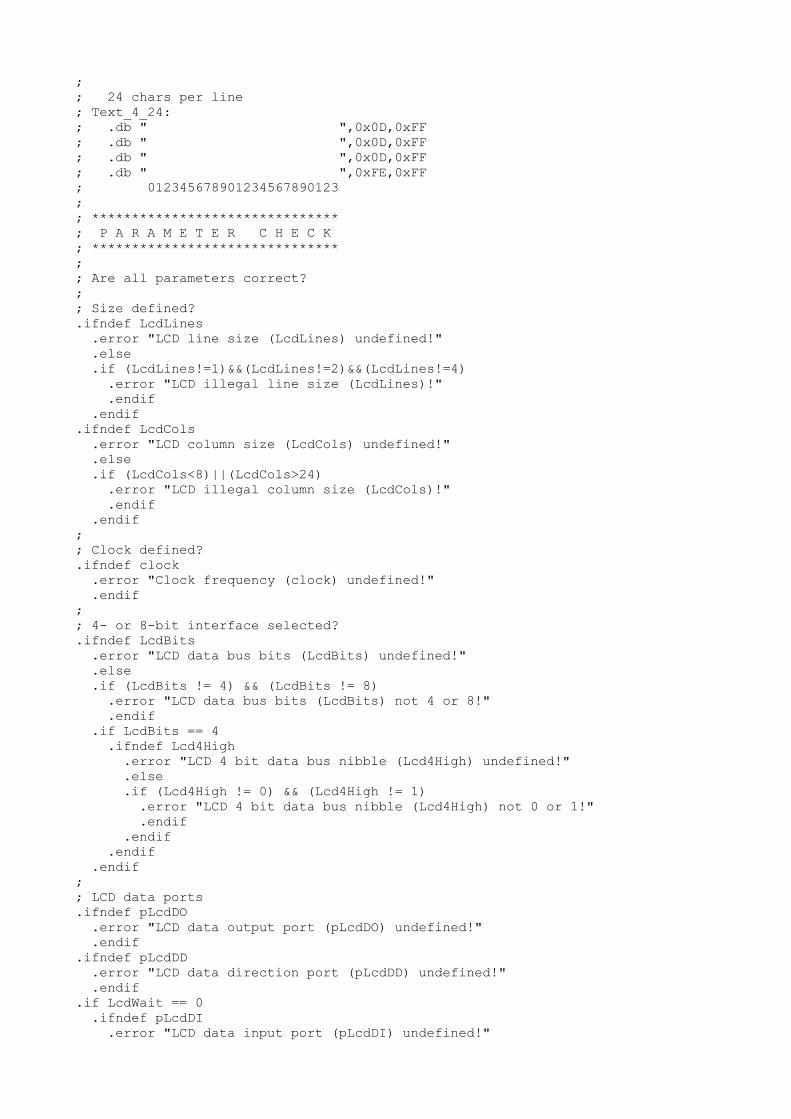
;; 24 chars per line; Text_4_24:; .db " ",0x0D,0xFF; .db " ",0x0D,0xFF; .db " ",0x0D,0xFF; .db " ",0xFE,0xFF; 012345678901234567890123;; *******************************; P A R A M E T E R C H E C K; *******************************;; Are all parameters correct?;; Size defined?.ifndef LcdLines .error "LCD line size (LcdLines) undefined!" .else .if (LcdLines!=1)&&(LcdLines!=2)&&(LcdLines!=4) .error "LCD illegal line size (LcdLines)!" .endif .endif.ifndef LcdCols .error "LCD column size (LcdCols) undefined!" .else .if (LcdCols<8)||(LcdCols>24) .error "LCD illegal column size (LcdCols)!" .endif .endif;; Clock defined?.ifndef clock .error "Clock frequency (clock) undefined!" .endif;; 4- or 8-bit interface selected?.ifndef LcdBits .error "LCD data bus bits (LcdBits) undefined!" .else .if (LcdBits != 4) && (LcdBits != 8) .error "LCD data bus bits (LcdBits) not 4 or 8!" .endif .if LcdBits == 4 .ifndef Lcd4High .error "LCD 4 bit data bus nibble (Lcd4High) undefined!" .else .if (Lcd4High != 0) && (Lcd4High != 1) .error "LCD 4 bit data bus nibble (Lcd4High) not 0 or 1!" .endif .endif .endif .endif;; LCD data ports.ifndef pLcdDO .error "LCD data output port (pLcdDO) undefined!" .endif.ifndef pLcdDD .error "LCD data direction port (pLcdDD) undefined!" .endif.if LcdWait == 0 .ifndef pLcdDI .error "LCD data input port (pLcdDI) undefined!"
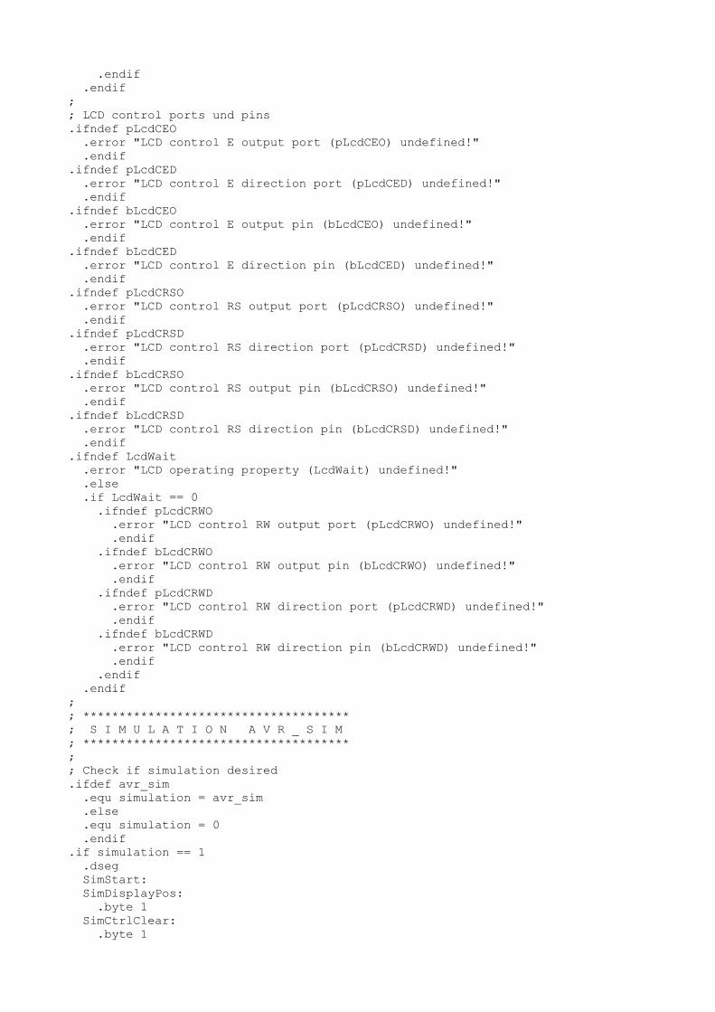
.endif .endif;; LCD control ports und pins.ifndef pLcdCEO .error "LCD control E output port (pLcdCEO) undefined!" .endif.ifndef pLcdCED .error "LCD control E direction port (pLcdCED) undefined!" .endif.ifndef bLcdCEO .error "LCD control E output pin (bLcdCEO) undefined!" .endif.ifndef bLcdCED .error "LCD control E direction pin (bLcdCED) undefined!" .endif.ifndef pLcdCRSO .error "LCD control RS output port (pLcdCRSO) undefined!" .endif.ifndef pLcdCRSD .error "LCD control RS direction port (pLcdCRSD) undefined!" .endif.ifndef bLcdCRSO .error "LCD control RS output pin (bLcdCRSO) undefined!" .endif.ifndef bLcdCRSD .error "LCD control RS direction pin (bLcdCRSD) undefined!" .endif.ifndef LcdWait .error "LCD operating property (LcdWait) undefined!" .else .if LcdWait == 0 .ifndef pLcdCRWO .error "LCD control RW output port (pLcdCRWO) undefined!" .endif .ifndef bLcdCRWO .error "LCD control RW output pin (bLcdCRWO) undefined!" .endif .ifndef pLcdCRWD .error "LCD control RW direction port (pLcdCRWD) undefined!" .endif .ifndef bLcdCRWD .error "LCD control RW direction pin (bLcdCRWD) undefined!" .endif .endif .endif;; *************************************; S I M U L A T I O N A V R _ S I M; *************************************;; Check if simulation desired.ifdef avr_sim .equ simulation = avr_sim .else .equ simulation = 0 .endif.if simulation == 1 .dseg SimStart: SimDisplayPos: .byte 1 SimCtrlClear: .byte 1
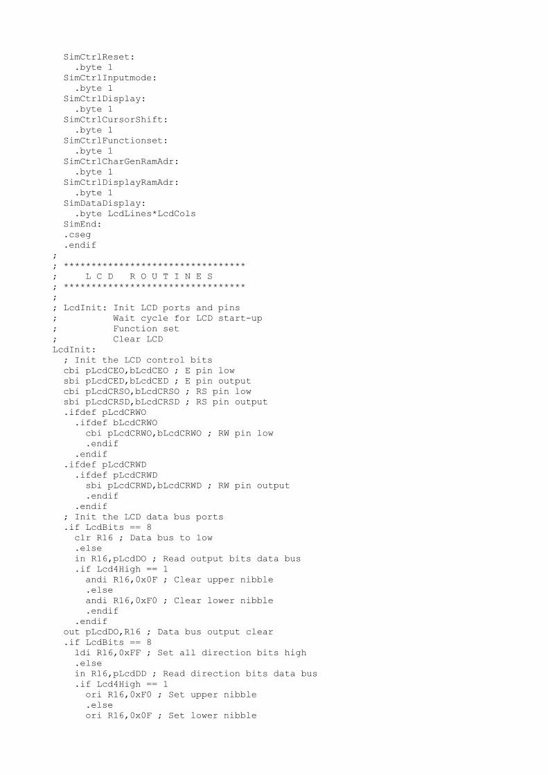
SimCtrlReset: .byte 1 SimCtrlInputmode: .byte 1 SimCtrlDisplay: .byte 1 SimCtrlCursorShift: .byte 1 SimCtrlFunctionset: .byte 1 SimCtrlCharGenRamAdr: .byte 1 SimCtrlDisplayRamAdr: .byte 1 SimDataDisplay: .byte LcdLines*LcdCols SimEnd: .cseg .endif;; *********************************; L C D R O U T I N E S; *********************************;; LcdInit: Init LCD ports and pins; Wait cycle for LCD start-up; Function set; Clear LCDLcdInit: ; Init the LCD control bits cbi pLcdCEO,bLcdCEO ; E pin low sbi pLcdCED,bLcdCED ; E pin output cbi pLcdCRSO,bLcdCRSO ; RS pin low sbi pLcdCRSD,bLcdCRSD ; RS pin output .ifdef pLcdCRWO .ifdef bLcdCRWO cbi pLcdCRWO,bLcdCRWO ; RW pin low .endif .endif .ifdef pLcdCRWD .ifdef pLcdCRWD sbi pLcdCRWD,bLcdCRWD ; RW pin output .endif .endif ; Init the LCD data bus ports .if LcdBits == 8 clr R16 ; Data bus to low .else in R16,pLcdDO ; Read output bits data bus .if Lcd4High == 1 andi R16,0x0F ; Clear upper nibble .else andi R16,0xF0 ; Clear lower nibble .endif .endif out pLcdDO,R16 ; Data bus output clear .if LcdBits == 8 ldi R16,0xFF ; Set all direction bits high .else in R16,pLcdDD ; Read direction bits data bus .if Lcd4High == 1 ori R16,0xF0 ; Set upper nibble .else ori R16,0x0F ; Set lower nibble
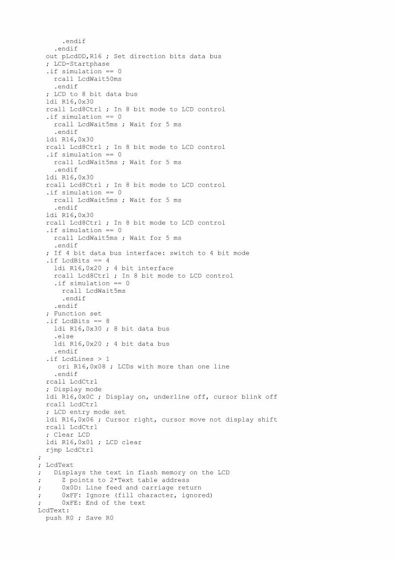
.endif .endif out pLcdDD,R16 ; Set direction bits data bus ; LCD-Startphase .if simulation == 0 rcall LcdWait50ms .endif ; LCD to 8 bit data bus ldi R16,0x30 rcall Lcd8Ctrl ; In 8 bit mode to LCD control .if simulation == 0 rcall LcdWait5ms ; Wait for 5 ms .endif ldi R16,0x30 rcall Lcd8Ctrl ; In 8 bit mode to LCD control .if simulation == 0 rcall LcdWait5ms ; Wait for 5 ms .endif ldi R16,0x30 rcall Lcd8Ctrl ; In 8 bit mode to LCD control .if simulation == 0 rcall LcdWait5ms ; Wait for 5 ms .endif ldi R16,0x30 rcall Lcd8Ctrl ; In 8 bit mode to LCD control .if simulation == 0 rcall LcdWait5ms ; Wait for 5 ms .endif ; If 4 bit data bus interface: switch to 4 bit mode .if LcdBits == 4 ldi R16,0x20 ; 4 bit interface rcall Lcd8Ctrl ; In 8 bit mode to LCD control .if simulation == 0 rcall LcdWait5ms .endif .endif ; Function set .if LcdBits == 8 ldi R16,0x30 ; 8 bit data bus .else ldi R16,0x20 ; 4 bit data bus .endif .if LcdLines > 1 ori R16,0x08 ; LCDs with more than one line .endif rcall LcdCtrl ; Display mode ldi R16,0x0C ; Display on, underline off, cursor blink off rcall LcdCtrl ; LCD entry mode set ldi R16,0x06 ; Cursor right, cursor move not display shift rcall LcdCtrl ; Clear LCD ldi R16,0x01 ; LCD clear rjmp LcdCtrl;; LcdText; Displays the text in flash memory on the LCD; Z points to 2*Text table address; 0x0D: Line feed and carriage return; 0xFF: Ignore (fill character, ignored); 0xFE: End of the textLcdText: push R0 ; Save R0

ldi R16,LcdLines ; Maximum line number mov R0,R16 ; to R0LcdText1: lpm R16,Z+ ; Read next char from flash cpi R16,0xFE ; End of text? breq LcdText3 ; Yes brcc LcdText1 ; Ignore fill characters cpi R16,0x0D ; Line feed and carriage return? brne LcdText2 ; No dec R0 ; Decrease line counter breq LcdText1 ; If zero, continue .if simulation == 1 ; CR/LF in SRAM memory push ZH ; Save Z push ZL push R16 ; Save character ldi ZH,High(SimDataDisplay) ; Perform newline ldi ZL,Low(SimDataDisplay) ldi R16,LcdLines LcdText1a: adiw ZL,LcdCols dec R16 cp R16,R0 brne LcdText1a ldi R16,Low(SimDataDisplay) sub ZL,R16 ldi R16,High(SimDataDisplay) sbc ZH,R16 sts SimDisplayPos,ZL pop R16 ; Restore character pop ZL ; Restore Z pop ZH .endif ; CR/LF on LCD push ZH ; Save Z push ZL ldi ZH,LcdLines ; Calculate line sub ZH,R0 clr ZL ; To line start rcall LcdPos ; Set LCD position pop ZL ; Restore Z pop ZH rjmp LcdText1 ; Next character in flashLcdText2: rcall LcdChar ; Character in R16 to LCD rjmp LcdText1 ; Next characterLcdText3: pop R0 ; Restore R0 ret;; LcdSRam displays text in SRAM at the current LCD position; Z points to SRAM address; R16: Number of charactersLcdSRam: push R16 ; Save R16 ld R16,Z+ ; Read character rcall LcdChar ; Display on LCD pop R16 ; Restore R16 dec R16 ; Downcount number of characters brne LcdSRam ; Further characters to display ret;; LcdChar displays character in R16 at the current position; R16: Character
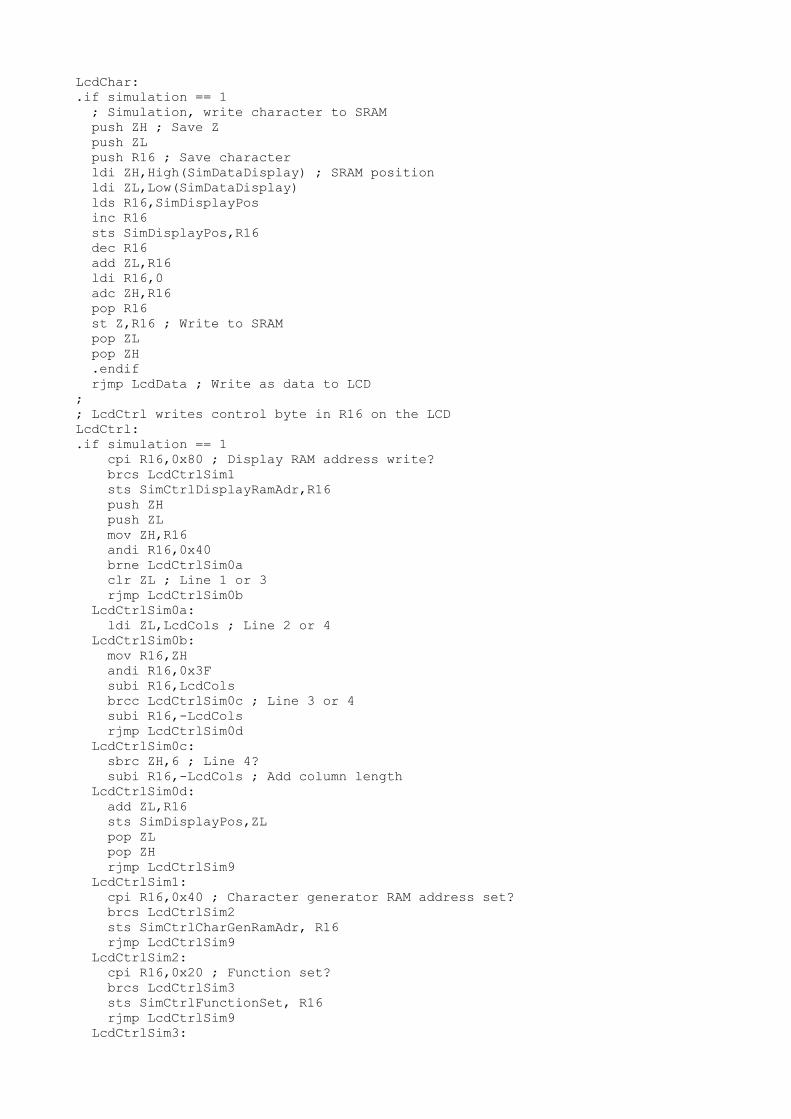
LcdChar:.if simulation == 1 ; Simulation, write character to SRAM push ZH ; Save Z push ZL push R16 ; Save character ldi ZH,High(SimDataDisplay) ; SRAM position ldi ZL,Low(SimDataDisplay) lds R16,SimDisplayPos inc R16 sts SimDisplayPos,R16 dec R16 add ZL,R16 ldi R16,0 adc ZH,R16 pop R16 st Z,R16 ; Write to SRAM pop ZL pop ZH .endif rjmp LcdData ; Write as data to LCD;; LcdCtrl writes control byte in R16 on the LCDLcdCtrl:.if simulation == 1 cpi R16,0x80 ; Display RAM address write? brcs LcdCtrlSim1 sts SimCtrlDisplayRamAdr,R16 push ZH push ZL mov ZH,R16 andi R16,0x40 brne LcdCtrlSim0a clr ZL ; Line 1 or 3 rjmp LcdCtrlSim0b LcdCtrlSim0a: ldi ZL,LcdCols ; Line 2 or 4 LcdCtrlSim0b: mov R16,ZH andi R16,0x3F subi R16,LcdCols brcc LcdCtrlSim0c ; Line 3 or 4 subi R16,-LcdCols rjmp LcdCtrlSim0d LcdCtrlSim0c: sbrc ZH,6 ; Line 4? subi R16,-LcdCols ; Add column length LcdCtrlSim0d: add ZL,R16 sts SimDisplayPos,ZL pop ZL pop ZH rjmp LcdCtrlSim9 LcdCtrlSim1: cpi R16,0x40 ; Character generator RAM address set? brcs LcdCtrlSim2 sts SimCtrlCharGenRamAdr, R16 rjmp LcdCtrlSim9 LcdCtrlSim2: cpi R16,0x20 ; Function set? brcs LcdCtrlSim3 sts SimCtrlFunctionSet, R16 rjmp LcdCtrlSim9 LcdCtrlSim3:

cpi R16,0x10 ; Cursor shift? brcs LcdCtrlSim4 sts SimCtrlCursorShift, R16 rjmp LcdCtrlSim9 LcdCtrlSim4: cpi R16,0x08 ; Display control set? brcs LcdCtrlSim5 sts SimCtrlDisplay, R16 rjmp LcdCtrlSim9 LcdCtrlSim5: cpi R16,0x04 ; Display control? brcs LcdCtrlSim6 sts SimCtrlInputmode, R16 rjmp LcdCtrlSim9 LcdCtrlSim6: cpi R16,0x02 ; Reset? brcs LcdCtrlSim7 sts SimCtrlReset,R16 rjmp LcdCtrlSim9 LcdCtrlSim7: cpi R16,0x01 ; Clear? brcs LcdCtrlSim8 sts SimCtrlClear,R16 ; LCD clear display push ZH push ZL ldi ZH,High(SimEnd) ldi ZL,Low(SimEnd) clr R16 LcdCtrl7a: st -Z,R16 ; Fill with zeroes backwards cpi ZL,Low(SimStart) brne LcdCtrl7a cpi ZH,High(SimStart) brne LcdCtrl7a ldi R16,0x01 pop ZL pop ZH rjmp LcdCtrlSim9 LcdCtrlSim8: ; 00 command LcdCtrlSim9: .endif .if LcdWait == 0 rcall LcdBusy ; Wait for busy flag clear .endif cbi pLcdCRSO,bLcdCRSO ; RS bit low .if LcdBits == 4 push ZL push R16 in ZL,pLcdDO ; Read data output port .if Lcd4High == 1 andi ZL,0x0F ; Clear upper nibble port andi R16,0xF0 ; Clear lower nibble R16 .else andi ZL,0xF0 ; Clear lower nibble port swap R16 ; Upper to lower nibble andi R16,0x0F ; Clear upper nibble R16 .endif or R16,ZL ; Combine out pLcdDO,R16 ; and output rcall LcdPulseE ; Activate E pop R16 ; R16 restore push R16 ; and save again in ZL,pLcdDO ; Read data output port

.if Lcd4High == 1 andi ZL,0x0F ; Preserve lower nibble of port swap R16 ; Lower to upper nibble R16 andi R16,0xF0 ; Preserve upper nibble R16 .else andi ZL,0xF0 ; Preserve upper nibble of port andi R16,0x0F ; Preserve lower nibble R16 .endif or R16,ZL ; Combine the two nibbles out pLcdDO,R16 ; To data bus rcall LcdPulseE ; Activate E pop R16 ; Restore R16 pop ZL ; Restore ZL .else out pLcdDO,R16 ; Input on data bus rcall LcdPulseE ; Activate E .endif .if LcdWait == 1 andi R16,0xFC ; The six upper bits of control command brne LcdCtrl1 ; are not zero, short delay rjmp LcdWait1640us ; Wait 1,64 ms LcdCtrl1: rjmp LcdWait40us ; Wait 40 us .else ret .endif;; LcdPos position the LCD cursor to the position in Z; ZH: Line (0 to number of lines - 1); ZL: Column (0 to number of colums per line - 1)LcdPos: cpi ZH,1 ; Line = 1? ldi R16,0x80 ; Address line 0 .if LcdLines < 2 ; LCD has only one line rjmp LcdPos1 .endif brcs LcdPos1 ; Line 1 ldi R16,0xC0 ; Line 2 address .if LcdLines == 2 rjmp LcdPos1 ; Lcd has only two lines .endif breq LcdPos1 ; Line 2 selected ldi R16,0x80+LcdCols ; Address line 3 cpi ZH,2 ; Line = 3 breq LcdPos1 ; Line 3 ldi R16,0xC0+LcdCols ; Address line 4LcdPos1: add R16,ZL ; Add column rjmp LcdCtrl ; Send as control to LCD;; LcdSpec generates special characters on the LCD; Z points to 2*Table address; Table format:; 1. byte: Address of character, 0b01zzz000,; 0: End of the table; 2. byte: Dummy character, ignored; 3. to 10 th byte: Pixel data of the lines 1 to 8LcdSpec: push R0 ; R0 is counterLcdSpec1: lpm R16,Z+ ; Read address of character tst R16 ; End of the table? breq LcdSpec3 ; Yes rcall LcdCtrl ; Write address
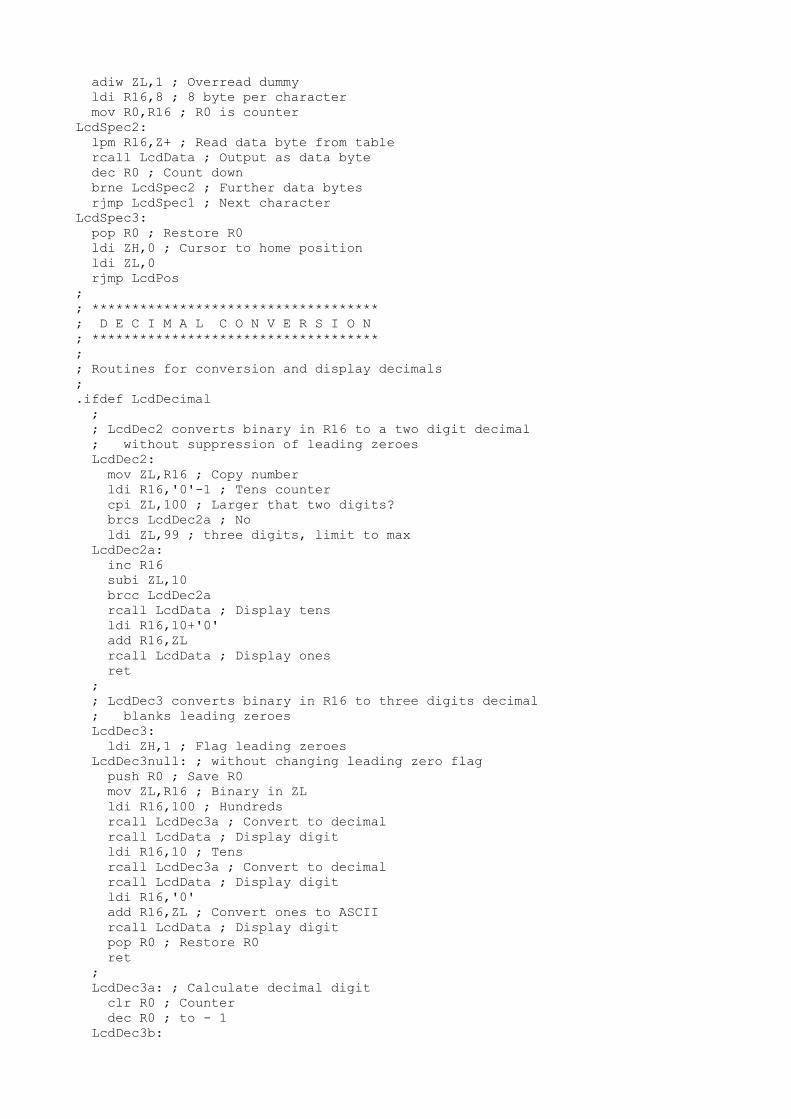
adiw ZL,1 ; Overread dummy ldi R16,8 ; 8 byte per character mov R0,R16 ; R0 is counterLcdSpec2: lpm R16,Z+ ; Read data byte from table rcall LcdData ; Output as data byte dec R0 ; Count down brne LcdSpec2 ; Further data bytes rjmp LcdSpec1 ; Next characterLcdSpec3: pop R0 ; Restore R0 ldi ZH,0 ; Cursor to home position ldi ZL,0 rjmp LcdPos;; ************************************; D E C I M A L C O N V E R S I O N; ************************************;; Routines for conversion and display decimals;.ifdef LcdDecimal ; ; LcdDec2 converts binary in R16 to a two digit decimal ; without suppression of leading zeroes LcdDec2: mov ZL,R16 ; Copy number ldi R16,'0'-1 ; Tens counter cpi ZL,100 ; Larger that two digits? brcs LcdDec2a ; No ldi ZL,99 ; three digits, limit to max LcdDec2a: inc R16 subi ZL,10 brcc LcdDec2a rcall LcdData ; Display tens ldi R16,10+'0' add R16,ZL rcall LcdData ; Display ones ret ; ; LcdDec3 converts binary in R16 to three digits decimal ; blanks leading zeroes LcdDec3: ldi ZH,1 ; Flag leading zeroes LcdDec3null: ; without changing leading zero flag push R0 ; Save R0 mov ZL,R16 ; Binary in ZL ldi R16,100 ; Hundreds rcall LcdDec3a ; Convert to decimal rcall LcdData ; Display digit ldi R16,10 ; Tens rcall LcdDec3a ; Convert to decimal rcall LcdData ; Display digit ldi R16,'0' add R16,ZL ; Convert ones to ASCII rcall LcdData ; Display digit pop R0 ; Restore R0 ret ; LcdDec3a: ; Calculate decimal digit clr R0 ; Counter dec R0 ; to - 1 LcdDec3b:
inc R0 ; Increase counter sub ZL,R16 ; Subtract 100 or 10 brcc LcdDec3b ; No overflow, continue add ZL,R16 ; Recover last subtraction tst R0 ; Digit zero? breq LcdDec3c ; Yes, check blanking clr ZH ; No blanking any more ldi R16,'0' ; ASCII-0 add R16,R0 ; Add counter ret LcdDec3c: tst ZH ; Zero blanking? breq LcdDec3d ; No ldi R16,' ' ; Blank char ret LcdDec3d: ldi R16,'0' ; Zero char ret ; ; LcdDec5 converts binary Z to five decimal digits ; blank leading zeroes LcdDec5: push R2 ; Save registers push R1 push R0 clr R2 ; Leading zeroes inc R2 ; Blanking on mov R1,ZH ; Copy binary to R1:R0 mov R0,ZL ldi ZH,High(10000) ; First decimal digit ldi ZL,Low(10000) rcall LcdDec5a ; Convert first digit ldi ZH,High(1000) ; Second decimal digit ldi ZL,Low(1000) rcall LcdDec5a ; Convert second digit ldi ZH,High(100) ; Third decimal digit ldi ZL,Low(100) rcall LcdDec5a ; Convert decimal digit ldi ZH,High(10) ; Fourth decimal digit ldi ZL,Low(10) rcall LcdDec5a ; Convert decimal digit ldi R16,'0' ; Convert fifth digit to ASCII add R16,R0 rcall LcdChar ; Display digit pop R0 ; Restore registers pop R1 pop R2 ret ; LcdDec5a: ; Convert to decimal digit ldi R16,'0'-1 ; To ASCII-0 - 1 LcdDec5b: inc R16 ; Increase counter sub R0,ZL ; Subtract decimal digit LSB sbc R1,ZH ; and MSB with Carry brcc LcdDec5b ; Repeat until carry add R0,ZL ; Take back last subtraction adc R1,ZH cpi R16,'0' ; Zero? breq LcdDec5c ; Yes, check blanking clr R2 ; End blanking rjmp LcdChar ; Display char in R16 LcdDec5c: tst R2 ; Blanking active?

breq LcdDec5d ; No ldi R16,' ' ; Blank character LcdDec5d: rjmp LcdChar ; Display char in R16 ; .endif;; ****************************************; H E X A D E C I M A L A U S G E B E N; ****************************************;; Routines for conversion and displaying hexadecimals;.ifdef LcdHex ; ; LcdHex2 converts binary in R16 to hexadecimal ; on the LCD LcdHex2: push R16 ; Is further needed swap R16 ; Upper nibble to lower nibble rcall LcdNibble ; Display lower nibble pop R16 ; Restore binary LcdNibble: andi R16,0x0F ; Clear upper nibble subi R16,-'0' ; Add ASCII-0 cpi R16,'9'+1 ; A to F? brcs LcdNibble1 ; No subi R16,-7 ; Add 7 LcdNibble1: rjmp LcdChar ; Display char on LCD ; ; LcdHex4 converts binary in Z to hexadecimal LcdHex4: mov R16,ZH ; MSB to R16 rcall LcdHex2 ; Display byte hexadecimal mov R16,ZL ; LSB to R16 rjmp LcdHex2 ; Display byte hexadecimal ; .endif;; *******************************; L C D S U B R O U T I N E S; *******************************;; Wait until LCD busy flag clear; needed only if wait mode is off.if LcdWait == 0 LcdBusy: push R16 ; Save R16 .if LcdBits == 8 clr R16 ; Data bus direction to input .else in R16,pLcdDD ; Read direction bits .if Lcd4High == 1 andi R16,0x0F ; Clear upper nibble .else andi R16,0xF0 ; Clear lower nibble .endif .endif out pLcdDD,R16 ; Write to direction port .if LcdBits == 8 clr R16 ; All output pins to low .else in R16,pLcdDO ; Read output port
.if Lcd4High == 1 andi R16,0x0F ; Clear upper nibble .else andi R16,0xF0 ; Clear lower nibble .endif .endif out pLcdDO,R16 ; Clear pull-Ups cbi pLcdCRSO,bLcdCRSO ; RS pin to low sbi pLcdCRWO,bLcdCRWO ; RW pin to high LcdBusyWait: rcall LcdIn ; Activate E, read data port, deactivate E .if LcdBits == 4 rcall LcdPulseE ; Dummy for lower nibble .endif lsl R16 ; Busy flag to carry brcs LcdBusyWait ; Flag = 1, wait on cbi pLcdCRWO,bLcdCRWO ; RW pin to low .if LcdBits == 8 ldi R16,0xFF ; Data to output .else in R16,pLcdDD ; Read direction data port .if Lcd4High == 1 ori R16,0xF0 ; Upper nibble high .else ori R16,0x0F ; Lower nibble high .endif .endif out pLcdDD,R16 ; Set direction port pop R16 ; Restore R16 ret ; Done ; ; Read busy flag to R16 ; Needed only if wait mode off LcdIn: cbi pLcdCRSO,bLcdCRSO ; LCD RS pin to low sbi pLcdCEO,bLcdCEO ; Set bit bLcdCEO on LCD control port nop ; Wait at least one clock cycle .if clock>1000000 ; Insert further NOPs for higher clocks nop .endif .if clock>2000000 nop .endif .if clock>3000000 nop .endif .if clock>3000000 nop .endif .if clock>4000000 nop .endif .if clock>5000000 nop .endif .if clock>6000000 nop .endif .if clock>7000000 nop .endif .if clock>8000000 nop .endif
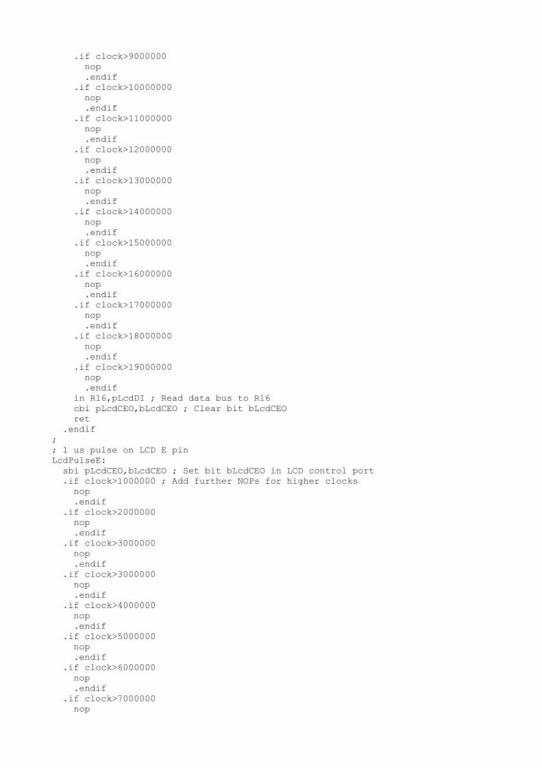
.if clock>9000000 nop .endif .if clock>10000000 nop .endif .if clock>11000000 nop .endif .if clock>12000000 nop .endif .if clock>13000000 nop .endif .if clock>14000000 nop .endif .if clock>15000000 nop .endif .if clock>16000000 nop .endif .if clock>17000000 nop .endif .if clock>18000000 nop .endif .if clock>19000000 nop .endif in R16,pLcdDI ; Read data bus to R16 cbi pLcdCEO,bLcdCEO ; Clear bit bLcdCEO ret .endif;; 1 us pulse on LCD E pinLcdPulseE: sbi pLcdCEO,bLcdCEO ; Set bit bLcdCEO in LCD control port .if clock>1000000 ; Add further NOPs for higher clocks nop .endif .if clock>2000000 nop .endif .if clock>3000000 nop .endif .if clock>3000000 nop .endif .if clock>4000000 nop .endif .if clock>5000000 nop .endif .if clock>6000000 nop .endif .if clock>7000000 nop

.endif .if clock>8000000 nop .endif .if clock>9000000 nop .endif .if clock>10000000 nop .endif .if clock>11000000 nop .endif .if clock>12000000 nop .endif .if clock>13000000 nop .endif .if clock>14000000 nop .endif .if clock>15000000 nop .endif .if clock>16000000 nop .endif .if clock>17000000 nop .endif .if clock>18000000 nop .endif .if clock>19000000 nop .endif cbi pLcdCEO,bLcdCEO ; Clear bit bLcdCEO ret;; Write R16 in 8 bit mode to LCD controlLcd8Ctrl: .if simulation == 1 push R16 clr R16 sts SimDisplayPos,R16 pop R16 .endif .if LcdBits == 4 push ZL ; Save ZL in ZL,pLcdDO ; Read data output port .if Lcd4High == 1 andi ZL,0x0F ; Clear upper nibble output andi R16,0xF0 ; Clear lower nibble R16 .else andi ZL,0xF0 ; Clear lower nibble output swap R16 ; Swap upper and lower nibble andi R16,0x0F ; Clear upper nibble R16 .endif or R16,ZL ; Combine pop ZL .endif out pLcdDO,R16 ; Data to LCD output port cbi pLcdCRSO,bLcdCRSO ; RS bit low

rjmp LcdPulseE ; Activate E;; LcdData: Write data in R16 to LCD; R16: Character or dataLcdData: .if LcdWait == 0 rcall LcdBusy ; Wait for busy flag of the LCD .endif sbi pLcdCRSO,bLcdCRSO ; Set RS bit .if LcdBits == 4 push ZL push R16 in ZL,pLcdDO ; Read data output port .if Lcd4High == 1 andi ZL,0x0F ; Clear upper nibble port andi R16,0xF0 ; Clear lower nibble R16 .else andi ZL,0xF0 ; Clear lower nibble port swap R16 ; Oberes und unteres Nibble vertauschen andi R16,0x0F ; Clear upper nibble R16 .endif or R16,ZL ; Combine out pLcdDO,R16 rcall LcdPulseE ; Activate E pop R16 ; Restore R16 push R16 ; and save again in ZL,pLcdDO ; Read data output port .if Lcd4High == 1 andi ZL,0x0F ; Preserve lower nibble of port swap R16 ; Upper to lower nibble andi R16,0xF0 ; Preserve upper nibble R16 .else andi ZL,0xF0 ; Preserve upper nibble port andi R16,0x0F ; Preserve lower nibble R16 .endif or R16,ZL ; Combine out pLcdDO,R16 ; To data bus rcall LcdPulseE ; Activate E pop R16 ; Restore R16 pop ZL ; Restore ZL .else out pLcdDO,R16 ; Byte to data bus rcall LcdPulseE ; Activate E .endif .if LcdWait == 1 rjmp LcdWait40us ; Wait for 40 us .endif ret;; ********************************; W A I T R O U T I N E S; ********************************;; Wait for 50 ms; At clock frequencies above 3.1 MHz the maximum; counting capability of Z exceeds its limit,; therefore the 50 ms calls the 5 ms delay 10; timesLcdWait50ms: push R16 ; Save R16 ldi R16,10 ; 10 times 5 msLcdWait50ms1: rcall LcdWait5ms ; Call 5 ms delay dec R16 ; Decrease counter
brne LcdWait50ms1 ; Repeat pop R16 ; Restore R16 ret;LcdWait5ms: ; Wait for 5 ms, RCALL 3 clock cycles .equ cLcdZ5ms = (5*clock/1000 - 18 + 2) / 4 push ZH ; Save ZH, + 2 cycles push ZL ; Save ZL, + 2 cycles ldi ZH,High(cLcdZ5ms) ; + 1 cycle ldi ZL,Low(cLcdZ5ms) ; + 1 cycle rjmp LcdWaitZ ; + 2 cycles ; Total: 11 clock cycles;.if LcdWait == 1 ; ; Wait routines necessary for wait mode ; Wait 1.64 ms .equ cLcdZ1640us = (164*(clock/1000)/100 - 18 + 2) / 4 LcdWait1640us: push ZH ; Save ZH push ZL ; Save ZL ldi ZH,High(cLcdZ1640us) ldi ZL,Low(cLcdZ1640us) rjmp LcdWaitZ ; ; Wait 40 us .equ cLcdZ40us = (40*clock/1000000 - 18 + 2) / 4 LcdWait40us: push ZH ; Save ZH push ZL ; Save ZL ldi ZH,High(cLcdZ40us) ldi ZL,Low(cLcdZ40us) rjmp LcdWaitZ .endif;; Wait routine for Z cyclesLcdWaitZ: ; 11 clock cycles sbiw ZL,1 ; Count down, +2 cycles brne LcdWaitZ ; If not zero: go on, + 2 cycles; if zero: 1 cycle pop ZL ; Restore ZL, +2 cycles pop ZH ; Restore ZH, +2 cycles ret ; Back, 4 cycles ; Total cycles: 11 + 4 * (Z - 1) + 3 + 8 ; ; Number cycles= 11 + 4 * (Z - 1) + 3 + 8 ; 11: RCALL, PUSH, PUSH, LDI, LDI, RJMP ; 4: 4 cycles per Z count (minus 1) ; 3: 3 cycles for last count ; 8: POP, RET ; = 4 * Z + 11 - 4 + 3 + 8 ; = 4 * Z + 18 ; Z = (Clock cycles - 18 + 2) / 4 ; +2: Rounding up during division by 4;; End of include file;

Path: Home => AVR-EN => Applications => LCD access with an AVR => Example 8 bit ATmega8AVR Applications
LCD Access withan AVR inassembler
Example application of"lcd.inc" 8 bit
Example application of lcd.inc in 8 bit mode on an ATmega8The assembler source code as shown here can be downloaded here in asmformat.
;; ************************************; * Test of the LCD include routines *; * (C)2018 avr-asm-tutorial.net *; ************************************;.nolist.include "m8def.inc" ; Define device ATmega8.list;; **********************************; H A R D W A R E; **********************************;; Device: ATmega8, Package: 28-pin-PDIP;; _________; 1 / |28; RESET o--|RES PC5|--o Key6-Ch4; LCD-D0 o--|PD0 PC4|--o Key5-Ch3; LCD-D1 o--|PD1 PC3|--o Key4-Ch2; LCD-D2 o--|PD2 PC2|--o Key3-Ch1; LCD-D3 o--|PD3 PC1|--o Key2-Start/Stop; LCD-D4 o--|PD4 PC0|--o Key1-Reset; VCC o--|VCC GND|--o GND; GND o--|GND AREF|--o NC; XTAL o--|XTAL1 AVCC|--o NC; 8.0 MHzo--|XTAL2 PB5|--o LCD-RW/SCK; LCD-D5 o--|PD5 PB4|--o LCD-RS/MISO; LCD-D6 o--|PD6 PB3|--o PB3/MOSI; LCD-D7 o--|PD7 PB2|--o LED-RED-Cath; LCD-E o--|PB0 PB1|--o LSP; |__________|;; **********************************; A D J U S T A B L E C O N S T; **********************************;; Standard parameter set of properties/definitions.equ clock = 8000000 ; Clock frequency of controller in Hz
; LCD size: .equ LcdLines = 4 ; Number of lines (1, 2, 4) .equ LcdCols = 20 ; Number of characters per line (8..24); LCD bus interface .equ LcdBits = 8 ; Bus size (4 or 8) ; If 4 bit bus: ;.equ Lcd4High = 1 ; Bus nibble (1=Upper, 0=Lower) .equ LcdWait = 0 ; Access mode (0 with busy, 1 with delay loops); LCD data ports .equ pLcdDO = PORTD ; Data output port .equ pLcdDD = DDRD ; Data direction port; LCD control ports und pins .equ pLcdCEO = PORTB ; Control E output port .equ bLcdCEO = PORTB0 ; Control E output portpin .equ pLcdCED = DDRB ; Control E direction port .equ bLcdCED = DDB0 ; Control E direction portpin .equ pLcdCRSO = PORTB ; Control RS output port .equ bLcdCRSO = PORTB4 ; Control RS output portpin .equ pLcdCRSD = DDRB ; Control RS direction port .equ bLcdCRSD = DDB4 ; Control RS direction portpin; If LcdWait = 0: .equ pLcdDI = PIND ; Data input port .equ pLcdCRWO = PORTB ; Control RW output port .equ bLcdCRWO = PORTB5 ; Control RW output portpin .equ pLcdCRWD = DDRB ; Control RW direction port .equ bLcdCRWD = DDB5 ; Control RW direction portpin; If you need binary to decimal conversion: .equ LcdDecimal = 1 ; If defined: include those routines; If you need binary to hexadecimal conversion: .equ LcdHex = 1 ; If defined: include those routines; If simulation in the SRAM is desired: ;.equ avr_sim = 1 ; 1=Simulate, 0 or undefined=Do not simulate;; **********************************; F I X & D E R I V. C O N S T; **********************************;;; **********************************; R E G I S T E R S; **********************************;.def rmp = R16;; **********************************; S R A M; **********************************;.dseg.org SRAM_START.byte 16;; **********************************; C O D E; **********************************;.cseg.org 000000;; **********************************; R E S E T & I N T - V E C T O R S; ********************************** rjmp Main ; Reset vector reti ; INT0
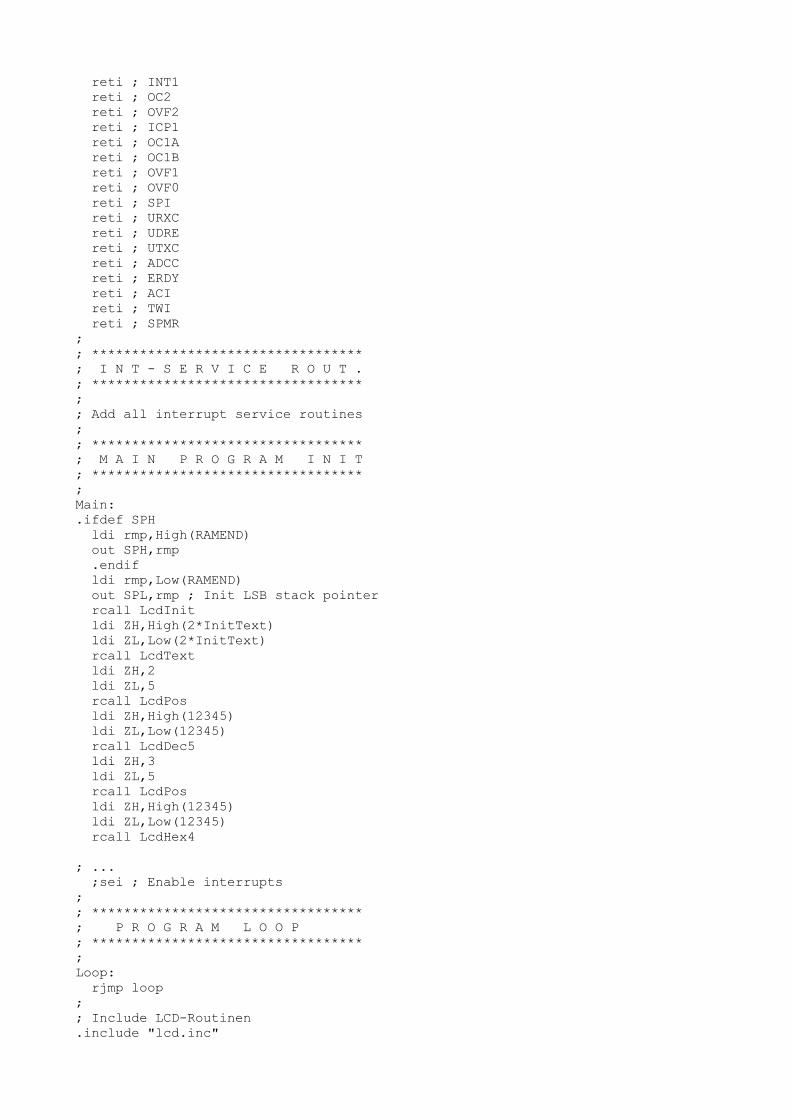
reti ; INT1 reti ; OC2 reti ; OVF2 reti ; ICP1 reti ; OC1A reti ; OC1B reti ; OVF1 reti ; OVF0 reti ; SPI reti ; URXC reti ; UDRE reti ; UTXC reti ; ADCC reti ; ERDY reti ; ACI reti ; TWI reti ; SPMR;; **********************************; I N T - S E R V I C E R O U T .; **********************************;; Add all interrupt service routines;; **********************************; M A I N P R O G R A M I N I T; **********************************;Main:.ifdef SPH ldi rmp,High(RAMEND) out SPH,rmp .endif ldi rmp,Low(RAMEND) out SPL,rmp ; Init LSB stack pointer rcall LcdInit ldi ZH,High(2*InitText) ldi ZL,Low(2*InitText) rcall LcdText ldi ZH,2 ldi ZL,5 rcall LcdPos ldi ZH,High(12345) ldi ZL,Low(12345) rcall LcdDec5 ldi ZH,3 ldi ZL,5 rcall LcdPos ldi ZH,High(12345) ldi ZL,Low(12345) rcall LcdHex4
; ... ;sei ; Enable interrupts;; **********************************; P R O G R A M L O O P; **********************************;Loop: rjmp loop;; Include LCD-Routinen.include "lcd.inc"

;InitText:.db "lcd.inc 8-bit busy",0x0D,0xFF.db "Display 4x20",0x0D,0xFF.db "Dec5=",0x0D.db "Hex4=",0x0D.db 0xFE,0xFF;;; End of source code;
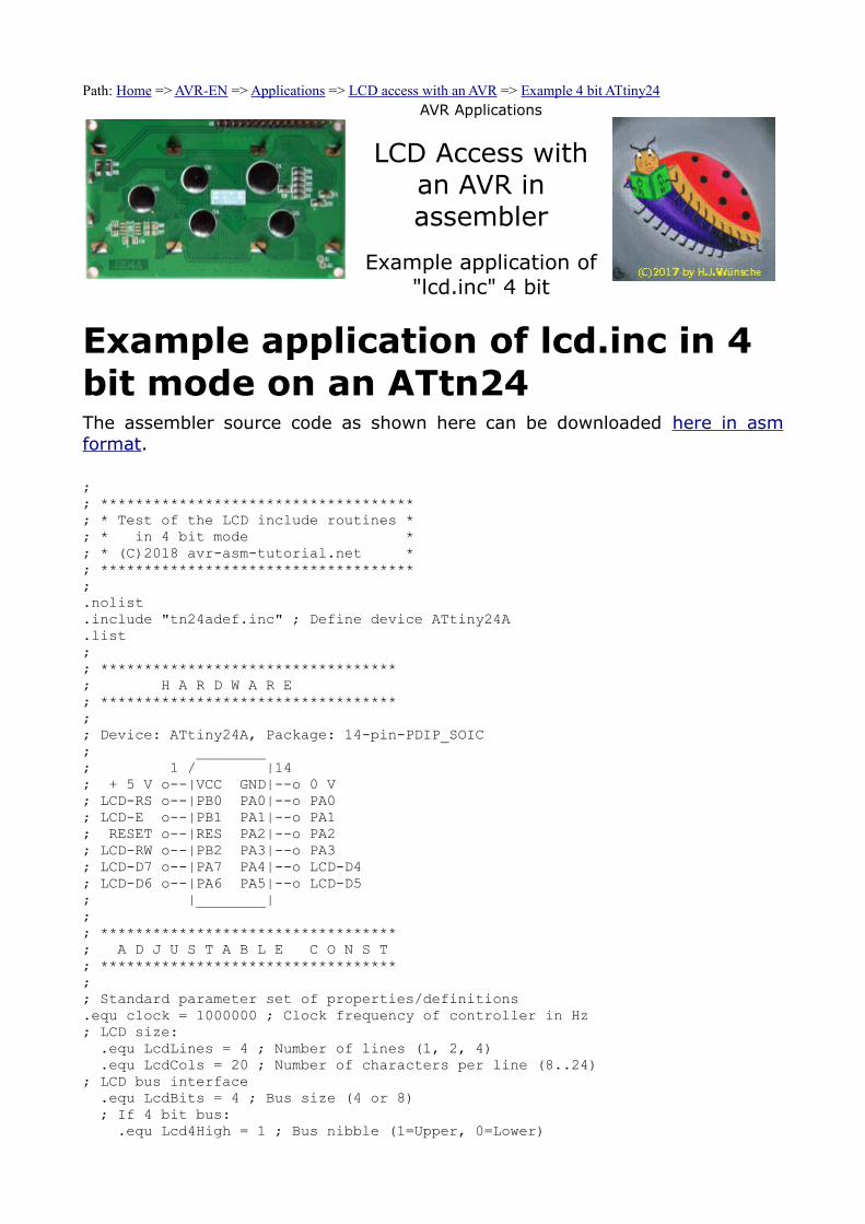
Path: Home => AVR-EN => Applications => LCD access with an AVR => Example 4 bit ATtiny24AVR Applications
LCD Access withan AVR inassembler
Example application of"lcd.inc" 4 bit
Example application of lcd.inc in 4 bit mode on an ATtn24The assembler source code as shown here can be downloaded here in asmformat.
;; ************************************; * Test of the LCD include routines *; * in 4 bit mode *; * (C)2018 avr-asm-tutorial.net *; ************************************;.nolist.include "tn24adef.inc" ; Define device ATtiny24A.list;; **********************************; H A R D W A R E; **********************************;; Device: ATtiny24A, Package: 14-pin-PDIP_SOIC; ________; 1 / |14; + 5 V o--|VCC GND|--o 0 V; LCD-RS o--|PB0 PA0|--o PA0; LCD-E o--|PB1 PA1|--o PA1; RESET o--|RES PA2|--o PA2; LCD-RW o--|PB2 PA3|--o PA3; LCD-D7 o--|PA7 PA4|--o LCD-D4; LCD-D6 o--|PA6 PA5|--o LCD-D5; |________|;; **********************************; A D J U S T A B L E C O N S T; **********************************;; Standard parameter set of properties/definitions.equ clock = 1000000 ; Clock frequency of controller in Hz; LCD size: .equ LcdLines = 4 ; Number of lines (1, 2, 4) .equ LcdCols = 20 ; Number of characters per line (8..24); LCD bus interface .equ LcdBits = 4 ; Bus size (4 or 8) ; If 4 bit bus: .equ Lcd4High = 1 ; Bus nibble (1=Upper, 0=Lower)
.equ LcdWait = 0 ; Access mode (0 with busy, 1 with delay loops); LCD data ports .equ pLcdDO = PORTA ; Data output port .equ pLcdDD = DDRA ; Data direction port; LCD control ports und pins .equ pLcdCEO = PORTB ; Control E output port .equ bLcdCEO = PORTB2 ; Control E output portpin .equ pLcdCED = DDRB ; Control E direction port .equ bLcdCED = DDB2 ; Control E direction portpin .equ pLcdCRSO = PORTB ; Control RS output port .equ bLcdCRSO = PORTB0 ; Control RS output portpin .equ pLcdCRSD = DDRB ; Control RS direction port .equ bLcdCRSD = DDB0 ; Control RS direction portpin; If LcdWait = 0: .equ pLcdDI = PINA ; Data input port .equ pLcdCRWO = PORTB ; Control RW output port .equ bLcdCRWO = PORTB1 ; Control RW output portpin .equ pLcdCRWD = DDRB ; Control RW direction port .equ bLcdCRWD = DDB1 ; Control RW direction portpin; If you need binary to decimal conversion: ;.equ LcdDecimal = 1 ; If defined: include those routines; If you need binary to hexadecimal conversion: ;.equ LcdHex = 1 ; If defined: include those routines; If simulation in the SRAM is desired: ;.equ avr_sim = 1 ; 1=Simulate, 0 or undefined=Do not simulate;; **********************************; F I X & D E R I V. C O N S T; **********************************;;; **********************************; R E G I S T E R S; **********************************;.def rmp = R16;; **********************************; S R A M; **********************************;.dseg.org SRAM_START.byte 16;; **********************************; C O D E; **********************************;.cseg.org 000000;; **********************************; R E S E T & I N T - V E C T O R S; **********************************; rjmp Main ; Reset vector; reti ; EXT_INT0; reti ; PCI0; reti ; PCI1; reti ; WATCHDOG; reti ; ICP1; reti ; OC1A; reti ; OC1B; reti ; OVF1

; reti ; OC0A; reti ; OC0B; reti ; OVF0; reti ; ACI; reti ; ADCC; reti ; ERDY; reti ; USI_STR; reti ; USI_OVF;; **********************************; I N T - S E R V I C E R O U T .; **********************************;; Add all interrupt service routines;; **********************************; M A I N P R O G R A M I N I T; **********************************;Main: ldi rmp,Low(RAMEND) out SPL,rmp ; Init LSB stack pointer rcall LcdInit ldi ZH,High(2*Codezeichen) ldi ZL,Low(2*Codezeichen) rcall LcdSpec ldi ZH,High(2*InitText) ldi ZL,Low(2*InitText) rcall LcdText; ... ;sei ; Enable interrupts;; **********************************; P R O G R A M L O O P; **********************************;Loop: rjmp loop;; Include LCD-Routinen.include "lcd.inc";InitText:.db "lcd.inc 4-bit busy",0x0D,0xFF.db "Display 4x20",0x0D,0xFF.db "Spezialzeichen:",0x0D.db 0x00,' ',0x01,' ',0x02,' ',0x03,' ',0x04,' ',0x05,' ',0x06,' ',0x07,0xFF.db 0xFE,0xFF
;; Table of code charactersCodezeichen:.db 64,0,0,12,6,31,6,12,0,0 ; Z = 0, arrow right.db 72,0,0,6,12,31,12,6,0,0 ; Z = 1, arrow left.db 80,0,4,14,31,21,4,4,4,0 ; Z = 2, arrow up.db 88,0,4,4,4,21,31,14,4,0 ; Z = 3, arrow down.db 96,0,0,15,3,5,9,16,0,0 ; Z = 4, arrow right up.db 104,0,0,16,9,5,3,15,0,0 ; Z = 5, arrow right down.db 112,0,0,1,18,20,24,30,0,0 ; Z = 6, arrow left down.db 120,0,0,30,24,20,18,1,0,0 ; Z = 7, arrow left up.db 0,0 ; End of table;
; End of source code