An Intelligent Interface Design Method Based on DSP and FPGA
4
An Intelligent Interface Design Method Based on DSP and FPGA Zhiyou Chi, Qingzhong Jia * , Xingdou Wang, Zongrui Liu and Ping Wu School of Aerospace Engineering, Beijing Institute of Technology, Beijing, China *Corresponding author Abstract—This paper which is based on the development of intelligent test platform and embedded processor technology, discuss configurable intelligent interface design method according to different interfaces of different test devices or even a same device, propose an intelligent interface design method based on DSP and FPGA and take asynchronous serial interface and analog interface as an example, list the intelligent design method of these interfaces. This method is a good application in the field of embedded interface design by its highly integrated, configurability and extensibility, which will make the versatility and portability of interface improved, likewise, the adaptability of test platform promoted. Keywords-test platform; embedded technology; intelligent interface I. INTRODUCTION At present, embedded electronic device is widely used in more and more area, meanwhile, the function and structure of which are becoming more and more comprehensive and complex, which leads to a question that traditional manual testing methods have been unable to meet the needs of modern electronic equipment testing. Therefore, the research and design of the automatic test platform is becoming one of the key tasks in the field of testing in the new area [1]. In the meantime, with the electronic device under test becoming much more complex and integrated, the amount and type of its interface are on the increase. According to different complex test pieces or the same test pieces with different interfaces, as well as the different channels of the same interface, test platform always needs to configure the interface due to requirements, for example, channel and length, and idle the rest redundant interfaces, to ensure the processing of upper layer data is convenient, and promote the adaptability of the test platform apart from the traversal method. In this paper, an embedded architecture based on DSP and FPGA is adopted in the development of test platform for the above purpose. On the basis of this architecture, taking the intelligent design of asynchronous serial interface and analog interface as an example, the design of the configurable interface achieves the goal of enhancing the adaptability of test platform. II. EMBEDDED INTELLIGENT INTERFACE FRAME STRUCTURE In the field of embedded applications, in the lower level design, large amount of data, data processing speed domains, relatively simple structures will be taken into account, in the higher level design, considering signal processing, complex algorithms, addressing flexibility, and powerful communication mechanism [2]. FPGA logic design can meet vast majority of the interface speed and bandwidth and DSP data processing can cover most of the upper layer algorithm, so the DSP plus FPGA architecture is now widely used in various embedded fields [3]. In this paper, based on the architecture of DSP and FPGA, the design methods of intelligent interface are discussed. A researching test platform architecture is proposed in Figure 1. The platform is connected to the host processing system via CPCI bus. DSP and FPGA act as the underlying architecture for this test platform interface module. In another words, the interfaces of measuring outside device enter into the test interface board through the CPCI custom pins, and go through level translation chips (for UART) and analog capture or output chips, then driven by the FPGA logic, data in requirement is sent to DSP for processing. After processing, the data is sent to upper layer processing system for operation or display and control through FPGA and CPCI bus. In Figure 1, as the local process module the interface module of DSP and FPGA is extended to CPCI bus via PCI_BRIDGE chip. FPGA module is formed by power module (POWER), storage FLASH, JTAG emulation. DSP module is mainly formed by power module (POWER), storage FLASH/ SDRAM, JTAG emulation. DSP and FPGA are connected together through EMIF interface. As one of the most common interfaces of DSP, EMIF stands for external memory interface. According to a certain rule and based on addressing method, EMIF interface arranges address for DSP own space and memory (FPGA itself is a SRAM) attached to DSP, DSP will access the memory by address mapping [4]. In Figure 2, taking the chip DSPC6713B as an example, it is assumed that its 20 address wires of CE3 space are connected to FPGA, in the case that control registers are set to 16-bit ASRAM mode, the address 0xb000_0002 is mapped as 0x0_0001 to the decode address of FPGA, whenever DSP access data of the outside interface, FPGA is only required to bind the external interface with 0x0_0001, DSP will obtain the interface data by accessing the address 0xb000_0002 itself. Similarly, all external interfaces are available to attach to the FPGA in this way. The design of intelligent interface aims at achieving the purpose of being selected and configurable, the embedded interfaces based on DSP and FPGA, will be discussed in details below. International Conference on Electrical, Mechanical and Industrial Engineering (ICEMIE 2016) © 2016. The authors - Published by Atlantis Press 318
Transcript of An Intelligent Interface Design Method Based on DSP and FPGA
An Intelligent Interface Design Method Based on DSP and FPGA
Zhiyou Chi, Qingzhong Jia*, Xingdou Wang, Zongrui Liu and Ping Wu School of Aerospace Engineering, Beijing Institute of Technology, Beijing, China
*Corresponding author
Abstract—This paper which is based on the development of intelligent test platform and embedded processor technology, discuss configurable intelligent interface design method according to different interfaces of different test devices or even a same device, propose an intelligent interface design method based on DSP and FPGA and take asynchronous serial interface and analog interface as an example, list the intelligent design method of these interfaces. This method is a good application in the field of embedded interface design by its highly integrated, configurability and extensibility, which will make the versatility and portability of interface improved, likewise, the adaptability of test platform promoted.
Keywords-test platform; embedded technology; intelligent interface
I. INTRODUCTION At present, embedded electronic device is widely used in
more and more area, meanwhile, the function and structure of which are becoming more and more comprehensive and complex, which leads to a question that traditional manual testing methods have been unable to meet the needs of modern electronic equipment testing. Therefore, the research and design of the automatic test platform is becoming one of the key tasks in the field of testing in the new area [1]. In the meantime, with the electronic device under test becoming much more complex and integrated, the amount and type of its interface are on the increase.
According to different complex test pieces or the same test pieces with different interfaces, as well as the different channels of the same interface, test platform always needs to configure the interface due to requirements, for example, channel and length, and idle the rest redundant interfaces, to ensure the processing of upper layer data is convenient, and promote the adaptability of the test platform apart from the traversal method.
In this paper, an embedded architecture based on DSP and FPGA is adopted in the development of test platform for the above purpose. On the basis of this architecture, taking the intelligent design of asynchronous serial interface and analog interface as an example, the design of the configurable interface achieves the goal of enhancing the adaptability of test platform.
II. EMBEDDED INTELLIGENT INTERFACE FRAME STRUCTURE In the field of embedded applications, in the lower level
design, large amount of data, data processing speed domains,
relatively simple structures will be taken into account, in the higher level design, considering signal processing, complex algorithms, addressing flexibility, and powerful communication mechanism [2]. FPGA logic design can meet vast majority of the interface speed and bandwidth and DSP data processing can cover most of the upper layer algorithm, so the DSP plus FPGA architecture is now widely used in various embedded fields [3].
In this paper, based on the architecture of DSP and FPGA, the design methods of intelligent interface are discussed. A researching test platform architecture is proposed in Figure 1. The platform is connected to the host processing system via CPCI bus. DSP and FPGA act as the underlying architecture for this test platform interface module. In another words, the interfaces of measuring outside device enter into the test interface board through the CPCI custom pins, and go through level translation chips (for UART) and analog capture or output chips, then driven by the FPGA logic, data in requirement is sent to DSP for processing. After processing, the data is sent to upper layer processing system for operation or display and control through FPGA and CPCI bus. In Figure 1, as the local process module the interface module of DSP and FPGA is extended to CPCI bus via PCI_BRIDGE chip. FPGA module is formed by power module (POWER), storage FLASH, JTAG emulation. DSP module is mainly formed by power module (POWER), storage FLASH/ SDRAM, JTAG emulation. DSP and FPGA are connected together through EMIF interface. As one of the most common interfaces of DSP, EMIF stands for external memory interface. According to a certain rule and based on addressing method, EMIF interface arranges address for DSP own space and memory (FPGA itself is a SRAM) attached to DSP, DSP will access the memory by address mapping [4]. In Figure 2, taking the chip DSPC6713B as an example, it is assumed that its 20 address wires of CE3 space are connected to FPGA, in the case that control registers are set to 16-bit ASRAM mode, the address 0xb000_0002 is mapped as 0x0_0001 to the decode address of FPGA, whenever DSP access data of the outside interface, FPGA is only required to bind the external interface with 0x0_0001, DSP will obtain the interface data by accessing the address 0xb000_0002 itself. Similarly, all external interfaces are available to attach to the FPGA in this way. The design of intelligent interface aims at achieving the purpose of being selected and configurable, the embedded interfaces based on DSP and FPGA, will be discussed in details below.
International Conference on Electrical, Mechanical and Industrial Engineering (ICEMIE 2016)
© 2016. The authors - Published by Atlantis Press 318

DSP
SDRA
MFLA
SHJTA
G
POWER
EMIF
FPGA
PCI_BRIDGE
EEPROM
CPCI
POWER JTAG
UART
AD
DA
LOCA
L
EMIF LO
GIC
EA
ED
CTRL
CHIPS/INTERFACE
UART
AD
UART
AD
DA DA
FLASH
FIGURE I. EMBEDDED INTELLIGENT INTERFACE STRUCTURE BASED ON DSP AND FPGA
DSP_EMIF
FPGA
0XB000_00020XB000_0004
0XB001_4002
0XB001_4004
0X0_0001
0X0_0002
0X0_A0010X0_A002
FIGURE II. EMIF ADDRESS MAPPING
III. INTELLIGENT DESIGN OF ASYNCHRONOUS SERIAL INTERFACE
Asynchronous serial interface, like UART, is a universal full-duplex communication interface, widely used in the PC and embedded field, including the test platform.
RX_FIFO
TX_FIFO
RX_FIFO_CFG_reg
TX_FIFO_CFG_reg
EMIF_LO
GIC
RX
TX
STOPBIT_CFG_reg
BAUD_GENERATORDIV_CFG_reg
RX
PARITYBIT_CFG_reg
STOPBIT_CFG_reg
TX
PARITYBIT_CFG_reg
RX_INT_reg
RX_INT_ENABLE_reg
TX_CHANNEL_reg
RX_INT
...reg
CTRL(CE/ARE/AWE...)
...reg
channel
int_en
int
fifo
stopbit
parity
buad
RX_addr
TX_addr
INT
DSP FPGA
EA
ED
FIGURE III. UART INTERFACE DESIGN CHART
319
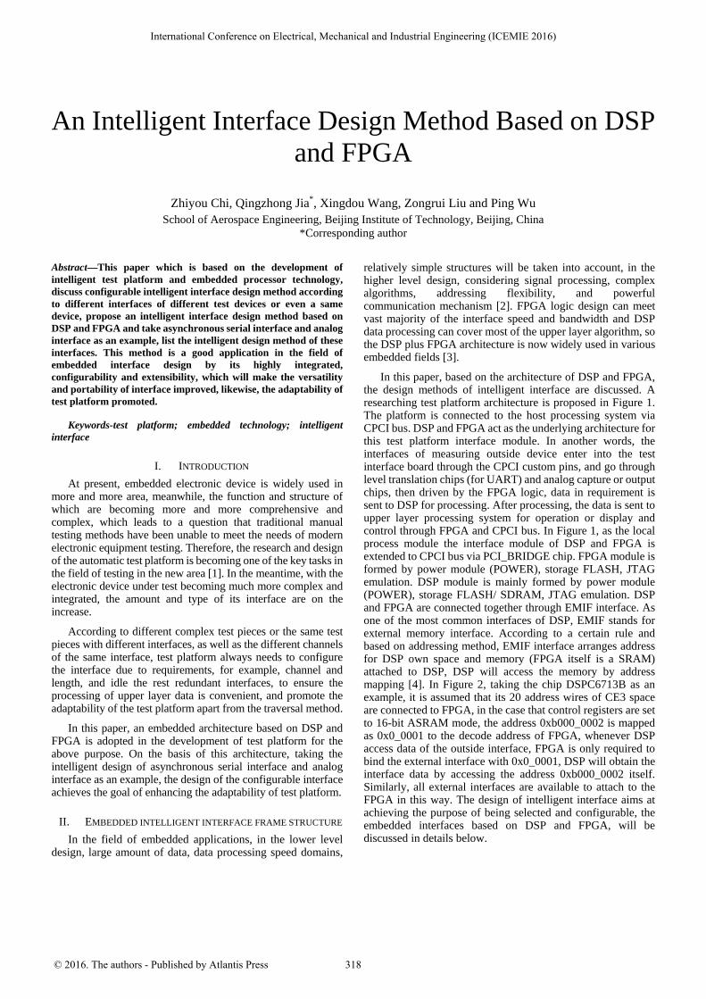
UART configurable parameters include baud rate,stop bits and parity. In practical applications, the multi-channel UART channel selection, FIFO depth and interrupt enabled are also considered. As shown in Figure 3, DSP configures the related parameters by addresses which EMIF defines in FPGA, which includes channel, interrupt enabled bit,FIFO depth,stop bits length, parity and baud rate, FPGA logic detects the corresponding address and receives configuration from EMIF. As for transmitting and receiving, baud rate, stop bit and parity are common parameters. Configuring DIV_CFG_reg will achieve different division rate in FPGA logic, leading to different baud rate, then SOPBIT_CFG_reg and PARITY_CFG_reg can configue different stop bits and parity mode. The transmitting or receiving buffer depth can be obtained by configuring FIFO_reg. For transmission, DSP sends transmission data to FPGA logic transmission buffer
TX_FIFO by the agreement address TX_addr. Upon receiption, DSP configures interrupt enabled bit to enable the selected channels to receive. When reaching receiving buffer RX_FIFO depth, FPGA sets the flag register RX_INT_reg and generates DSP interrupt, DSP querys interrupt source to obtain data from the selected channel via RX_addr and clears the interrupt flag. It is said UART is designed to achieve the UART transmission process communication and configure application parameters, in order to enhance the adaptability UART interface.
IV. INTELLIGENT DESIGN OF ANALOG INTERFACE Since the tested objects always appear in the form of analog,
such as voltage, current, analog interface includes analog acquisition and analog output. The method of design intelligent analog interface is also based on the principle that analog interface can be configured.
DSP
Channel_1Channel_2
Channel_3
Channel_n
...
ANALOG INPUT INTERFACEEMIFDSP
CHANNEL_addr
SINGLE:
DMA:
FIFO_CFG_reg
DSP EMIFANALOG INPUT INTERFACE
AD_FIFOCONVERT
CONVERT
CHANNEL_SEL_reg
AD_INT_MASK_reg...reg
AD_INT
TRIG
TRIG
PING_PONG
FPGA
FPGA
AD_ADDR
FIGURE IV. ANALOG INPUT INTERFACE DESIGN CHART
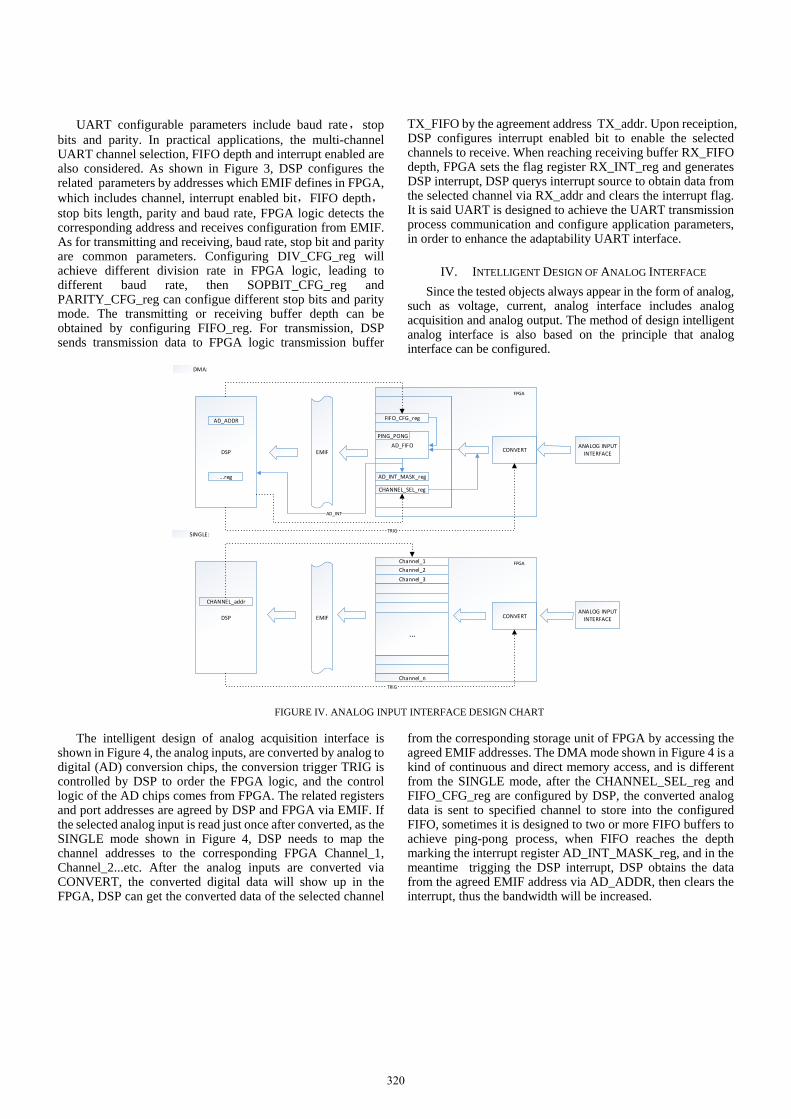
The intelligent design of analog acquisition interface is shown in Figure 4, the analog inputs, are converted by analog to digital (AD) conversion chips, the conversion trigger TRIG is controlled by DSP to order the FPGA logic, and the control logic of the AD chips comes from FPGA. The related registers and port addresses are agreed by DSP and FPGA via EMIF. If the selected analog input is read just once after converted, as the SINGLE mode shown in Figure 4, DSP needs to map the channel addresses to the corresponding FPGA Channel_1, Channel_2...etc. After the analog inputs are converted via CONVERT, the converted digital data will show up in the FPGA, DSP can get the converted data of the selected channel
from the corresponding storage unit of FPGA by accessing the agreed EMIF addresses. The DMA mode shown in Figure 4 is a kind of continuous and direct memory access, and is different from the SINGLE mode, after the CHANNEL_SEL_reg and FIFO_CFG_reg are configured by DSP, the converted analog data is sent to specified channel to store into the configured FIFO, sometimes it is designed to two or more FIFO buffers to achieve ping-pong process, when FIFO reaches the depth marking the interrupt register AD_INT_MASK_reg, and in the meantime trigging the DSP interrupt, DSP obtains the data from the agreed EMIF address via AD_ADDR, then clears the interrupt, thus the bandwidth will be increased.
320

Periodic:
Non periodic:
DSP
PERIOD_reg
DA_FIFO
EMIF
DA_CONVERT DA_INTERFACE
PING_PONG
CHANNEL_reg
DSP
DA_BUFFER
EMIF
DA_CONVERT DA_INTERFACE
CHANNEL_reg
delay_time
FPGA
FPGA
DA_ADDR
DA_ADDR
FIGURE V. ANALOG OUTPUT DESIGN CHART
Analog output interface (DA) approaches to intelligent design as shown in Figure 5, the conversion logic DA_CONVERT is controlled by FPGA. The analog output routes to an external device under test, can be divided into periodic and non-periodic output via CPCI bus. Periodic output is showed in the figure. According to the EMIF address DA_ADDR, DSP sends the data to FPGA digital-analog conversion buffer FIFO, then the FPGA digital to analog conversion logic depends on the specified cycle time defined by DSP, as well as the FIFO depth, PERIOD_reg and CHANNEL_reg, which defined to achieve channel selection and configuration period. Considering analog to digital conversion, FIFO sometimes is more than one piece to obtain higher speed. For non-periodic output, DSP makes a single transmission to send each non-cycle periods data to FPGA conversion cache, and controls each non-period cycle delay_time, then FPGA conversion logic selects specified channel and outputs analog signal according to the CHANNEL reg.
V. SUMMARY On the background of the development of test platform and
aiming at electronic devices, which are becoming increasingly complex, as with their interface, considering the adaptability, this paper designs intelligent interface based on DSP and FPGA, in order to meet the needs of different occasions. Two common interfaces intelligent design details are discussed in this paper, which have certain significance to the increase of modern electronic equipment interface intelligence. Future intelligent interface design is based on not only embedded technology, but also operating system and network will lead the electronic equipment interface into a more intelligent era.
REFERENCES [1] Fujun Lu, Deyong Cai, Chen Meng, Research Progress of Next
Generation Automatic Test System Architecture. Computer Measurement & Control, 23 (2015) 339-340.
[2] Zexi HAN, Yanni Sun, The technology of DSP and FPGA, Electronic Technology, 2 (2007) 18-19.
[3] Yin Wang, Kai Zhang, Jinping Dong, FPGA based expanded circuit design for DSP signal processing, The Fifth International Conference on Intelligent Systems Design and Engineering Applications, 2014, pp. 511-512.
[4] Texas Instruments, TMS320C6000 DSP external memory interface reference guide datasheet, pp. 87-89.
321