AECHI ECIURES APIC A GGB.ITH FCB J GEB A EE … · 95 95 98 99 I00 I00 I01 I01 I01 107 108 ......
161
AECHI_ECIURES APIC A_GGB.ITH_ FCB _IN_AE J_GEB_A EE_CE_SC_S Frcg_es_ F_o_t ICal:negie-Mellon _x:iv.) 160 ; a_ail: H_.IS _C ACB/MF At1 CSCL 09B G3/61 NB7-26.= 15 https://ntrs.nasa.gov/search.jsp?R=19870017082 2018-08-26T09:38:21+00:00Z
Transcript of AECHI ECIURES APIC A GGB.ITH FCB J GEB A EE … · 95 95 98 99 I00 I00 I01 I01 I01 107 108 ......
AECHI_ECIURES APIC A_GGB.ITH_ FCB _IN_AE
J_GEB_A EE_CE_SC_S Frcg_es_ F_o_tICal:negie-Mellon _x:iv.) 160 ; a_ail: H_.IS
_C ACB/MF At1 CSCL 09B G3/61
NB7-26.= 15
https://ntrs.nasa.gov/search.jsp?R=19870017082 2018-08-26T09:38:21+00:00Z
I
I
ir
II
I
I
II
II
II
II
II
Iili__ \,
/Progress Report
Grant NAG-I-575
/_-_/
NOVEL PARALLEL ARCHITECTURES AND
ALGORITHMS FOR LINEAR ALGEBRAPROCESSORS
Submitted to:
NASA Langley Research Center
Hampton, VA. 23665ATI_ENTION: John Shoosmith
Submitted by:
Prof. David Casasent _, ,Carnegie Mellon University
Department of Electrical and Computer Engineering
Pittsburgh, PA 15213
Principal Investigator: Professor David Casasent
Telephone: (412) 268-2464
April 1987
I
I
II
I
II
III
II
II
II
II
Table of Contents
ABSTRACT
1. INTRODUCTION
1.1 Overview
1.2 Number Representation
1.3 Laboratory System Design, Fabrication, and Algorithms1.4 Case Studies
1.5 Numerical Extensions
2. BIPOLAR BIASING IN HIGH ACCURACY OPTICAL
ALGEBRA PROCESSORS
2.1 Introduction
2.2 The method of biasing
2.3 Summary
3. OPTICAL LINEAR ALGEBRA PROCESSOR: LABORATORYPERFORMANCE FOR OPTIMAL CONTROL APPLICATIONS
3.1 Introduction
3.2 Space Integrating Optical Linear Algebra Processor
3.3 Number Representation and Electronic Support
3.4 Case Study and Algorithm
3.5 Laboratory Results
3.6 Summary and Conclusion
LINEAR
SYSTEM
4. REAL-TIME OPTICAL LABORATORY LINEAR ALGEBRA SOLUTION
OF PARTIAL DIFFERENTIAL EQUATIONS
4.1 Introduction
4.20lap Architecture and Fabrication
4.3 System Properties and Use4.4 Problem Definition
4.4.1 Explicit 1-D M-V Solution
4.4.2 Implicit LAE Solution
4.4.3 Explicit Matrix-Vector 2-D Solution
4.5 Case Study
4.6 Optical Realization Issues
4.6.1 Node Numbering
4.6.2 Partitioning and Data Flow
4.{}.3 Partitioning
4.6.4 High-Accuracy Encoding
4.6.5 High-Accuracy Data Flow and Partitioning
4.6.6 Performance Measures
4.7 Laboratory Test Results
4.7.1 Implicit vs. Explicit Solutions with Computational/System Errors Included
4.7.2 Implicit Algorithm with Variable Time Step Size
4.7.3 Analog System Laboratory Performance
4.7.4 Encoded High-Accuracy Laboratory System Performance
4.7.5 Quantitative Individual High-Accuracy Multiplication Data
4.7.6 Graphical 2-D Temporal Temperature Data Results
1
2
2
2
3
4
4
5
5
6
9
10
10
10
11
13
16
2O
23
23
23
25
26
27
28
29
30
32
32
32
34
35
36
36
37
37
38
39
39
42
43
I
5. TIME AND SPACE INTEGRATING
MATRIX-VECTOR ARRAY PROCESSOR
5.1 Introduction
5.2 Architecture Review
5.3 Number Representation
5.4 Partitioning, LU Decomposition and Accuracy Tradeoffs
5.4.1 Diagonal Partitioning
5.4.2 Output P3 Flexible Detector System
5.4.3 LU One-Channel Algorithm {}
5.4.4 Accuracy Above the Number of Channels by Partitioning
5.5 General Laboratory Electronic Support System Requirements
5.6 Electro-Optical Laboratory System
5.7 Finite Element Case Study
5.8 Laboratory System Data
5.9 Summary and Conclusion
6. Multi-channel Encoded System Design and Fabrication
6.1 Architecture
6.2 Electronic Support Requirements for Multi-Channel Encoded System
6.2.1 AO Cells and A/D Converters
6.2.2 Input Data Requirements
6.2.3 Detector P3 Requirements (future and now)
6.3 Host Computer System
6.3.1 Computer System
6.3.2 High Speed Memories6.4 Multi-Channel Encoded Processor Hardware
6.4.1 Clock Board
6.4.2 Mux/DeMux Board
6.4.3 ECL Shift/Add Board
6.4.4 100 MHz 6-bit A/D Boards
6.4.5 A/D Reference Supply
6.4.6 Four-Bit 200 MHz D/A Converter Boards6.4.7 RF Drivers and Oscillators
6.5 Detector Array and Fiber Optic Coupling
6.6 Software
6.7 Low Level Routines
6.7.1 Data Handling Conventions
6.7.2 Hardware Dependent Routines
6.7.3 Scalar Multiply Routines
6.7.4 LU Decomposition _oftware6.7.5 Software list
6.8 Initial Laboratory System
6.9 Single Bit Test System
6.9.1 Construction
6.9.2 Results
6.10 Three Channel System6.10.1 Construction
OPTICAL LABORATORY 48
48
49
50
52
52
53
54
55
56
57
57
60
63
65
65
67
67
69
69
73
74
77
79
80
81
82
85
87
88
89
91
93
95
95
98
99
I00
I00
I01
I01
I01
107
108
108
!

..o
111
I
iIi
II
I
6.10.2 Results 111
6.11 Summary 114
7. LABORATORY OLAP PERFORMANCE AND PLANS 118
7.1 Laboratory OLAP Characterization 118
7.1.1 Laboratory OLAP System Review 118
7.1.2 System Performance Limitations 121
7.2 AC-Coupled OLAP 123
7.2.1 AC Coupling Basics 1247.2.2 Laser Diode Modulation 124
7.2.3 Laser Diode Imaging Optics 126
7.2.4 AC Coupled Detector System 1277.3 Future Plans 128
8. CASE STUDIES FOR SIMULATION AND TESTNG OF THE OPTICAL 129
LINEAR ALGEBRA PROCESSOR
8.1 Introduction 129
8.2 Computational Fluid Dynamics 129
8.2.1 Nonlinear, Steady-State CFD 130
8.2.2 Nonlinear, Transient CFD 134
8.3 CFD Summary 135
8.4 Linear Dynamic Structural Mechanics Case Study 136
8.4.1 Linear Dynamic Analysis 138
9. OPTICAL PROCESSING EXTENSIONS 140
10. SUMMARY AND FUTURE WORK 142
I. POST-DETECTION HARDWARE DESIGN 143
1.1 Introduction 143
1.2 Basic OLAP output hardware 143
1.2.1 Case 1: radix is positive or negative and a power of 2 145
1.2.2 Case 2: Radix is positive or negative and not a power of 2 147
1.3 Future OLAP Detection Systems 150
1.4 Conclusions and Summary 152
I

iv
Figure
Figure
Figure
Figure
Figure
Figure
Figure
Figure
Figure
Figure
Figure
Figure
Figure
Figure
Figure
Figure
Figure
Figure
Figure
Figure
Figure
Figure
Figure
Figure
Figure
Figure
Figure
Figure
Figure
Figure
Figure
Figure
Figure
Figure
Figure
Figure
Figure
Figure
3-1:
3-2:
3-3:
3-4:
3-5:
3-6:
3-7:
3-8:
3-9:
4-1:
4-2:
4-3:
4-4:
4-5:
5-1:
5-2:
5-3:
6-1:
6-2:
6-3:
6-4:
6-5:
6-6:
6-7:
6-8:
6-9:
6-10:
6-11:
6-12:
6-13:
6-14:
6-15:6-16:
6-17:
6-18:
6-19:
6-20:
6-21:
List of Figures
Simplified schematic of the space integrating optical linear algebra 14
processor.
Details of one point modulator laser diode and collimating optics 14
system.
Photograph of the optical laboratory system. 15
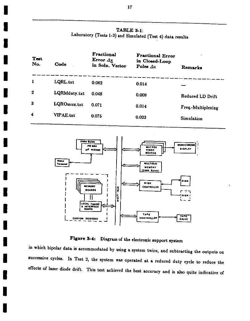
Diagram of the electronic support system 17
Photograph of the electronic support system. 18
Data flow arrangement for partitioning 19
Linear analog performance of 10 bits (0.1%). 20
Linear analog frequency-multiplexed performance. 21
Frequency-multiplexed optical interconnection architecture. 22
Simplified schematic of the space integrating optical linear algebra 25
processor.
Structure for the matrix in the implicit 2-D diffusion equation solution 31
Multi-processor architecture for multiple banded matrices 33
Data sequence for updating of explicit M-V formulation of 2-D diffusion 34PDE
Data flow for the high-accuracy multiplication (the example shown is for 35
the product of two 5-digit numbers)
Multi-Channel High Accuracy Time and Space Integrating Architecture 6 50
One-Channel LU Decomposition Architecture for Matrix Decomposition 6 52
Output P3 Detector System with Number Representation and 53
Component Flexibility and with a New Conversion Algorithm AbilityMulti-Channel AO CellArchitecture 66
Diagram of acoustic gaps from P1 and data inputs to P2 68
Diagram of the Mixed-Binary to Binary Converter 72
Operation Performed by Mixed-Binary to Binary Converter 73
System Block Diagram 75
Photograph of the Intel 86/380 System 76Board Layout for Intel Multibus 1 Chassis 77
High Speed Analog Hardware, Block Diagram 80
Picture of the ECL shift/add board 83
Control Section Block Diagram 84
Photograph of one 6 Bit, 100 MHz A/D board 87
Four bit D/A generating a random output 90
Photograph of the detector box used 94
Photograph of the SELFOC/fiber-optic setup 94
9 Bit Multiply on an 3 Bit Optical System 96
Assumed Decimal Point Handling 98
SingleChannel Test System 102
Detector output from the timing setup program 106
Test outputs from the singlechannel testsystem 108
Example RF inputsto the AO cells 113
Example detectoroutputs 113

Figure
Figure
Figure
Figure
Figure
Figure
Figure
Figure
Figure
Figure
Figure
Figure
Figure
Figure
Figure
Figure
Figure
6-22:
6-23:
6-24:
7-1:
7-2:
7-3:
8-1:
8-2:
8-3:
8-4:
I-1:
I-2:
I-3:
I-4:
I-5:
I-8:
I-7:
Action performed by the shift/add on the example problem
Example mixed binary outputs
Example system final output
Laboratory Optical System Schematic
Laboratory System Block Diagram
Laser Diode Operation Curve
Flow in a Driven Cavity
Discretized Driven Cavity DomainBeam element
Case study structure model
OLAP output configuration
Case 1: Forming binary Z from N binary words, c i
Shift/Add procedure when R_3
Expressing Z of base r_---2,3, etc. as base r_+2.
OLAP detection system and conversion unitFuture back-end hardware
Future post-detection hardware with two-levels of CCDs
114
115
115
119
120
125
130
131
136
137
144
146
148
149
150
151
152

ABSTRACT
Research done at the Carnegie Mellon Center for Excellence in Optical Data Processing for
Nasa Langley is reviewed, and the work proposed for the third year is detailed. The report
covers number representations, processing architectures and algorithms, optical linear algebra
processor fabrication and test results, case study descriptions, and future system plans.
I
II
I
III
I
I
1. INTRODUCTION
i
I
I
I
I
I
I
I
I
1.1 Overview
This report describes the current status of the research work done at the Carnegie Mellon
Center for Excellence in Optical Data Processing for Nasa Langley. This chapter is an overview
of the report. In the first year of the research contract, progress was made in developing: new
number representations, a new processing architecture and LU decomposition algorithm, and
error source modelling. In the second year, fabrication and test of a prototype system was
performed, along with extensions from some of the first year topics. These research efforts are
detailed herein. Much was learned in the development and operation of the prototype system,
and an evaluation of the system was made resulting in an improved laboratory processing
system. New numerical extensions of the optical system are proposed.
Brief summaries of the topics of this report follow in the rest of this chapter. A detailed
explanation is provided in subsequent chapters.
1.2 Number Representation
The processing of bipolar data is an important issue for optical data processing systems.
Most optical processing architectures modulate the intensity of light. Since this intensity cannot
be NnegativeU, bipolar data must somehow be incorporated into the processing. In the first year
of research, two methods of bipolar data encoding were developed. The first method was based
on twos-complement encoding 1, with new processing in the back end of the processor included to
improve the effeciency of conventional twos-complement encoding techniques 2'3. The second
method used negative base encoding for processing bipolar data 4. In this report we describe a
third method which is based on biasing the input data to the processor. This method is detailed
in Chapter 2.

iI
i
IiI
II
1.3 Laboratory System Design, Fabrication, and Algorithms
The step-by-step development of the laboratory systems and the use of various algorithms
and case studies is an important aspect of our optical computing research. It helps to better
evaluate our system design, error source models, and many practical issues. The first acousto-
optic (AO) based processor fabricated 5 was a five-channel analog frequency-multiplexed
processor. This processor was used to obtain an iterative analog solution to a matrix-vector
problem. This is described in Chapter 3. The processor was then used to implement an explicit
solution method to sovle a parabolic PDE case study, as described in Chapter 4.
We now focused our attention on case studies which require implicit solution methods, i.e.
those which often yield the more stable and accurate results. We also moved to encoded number
representations on the laboratory system. This provided us with a reduced dynamic range
requirement for the processor, and thus much more tolerance of processor error sources. We
concentrated on a new multi-channel system architecture 6, and fabricated a small cross-section
of the full multi-channel system, which was our prototype processor. We demonstrated this new
laboratory system by running a structural dynamics finite element plate bending case study on
the processor. The description of the laboratory system, data, performance, and other details is
provided in Chapter 5. The fabrication of the prototype processor, including optics and
electronics, and the software control of the system are described in Chapter 6. Use of the
laboratory system resulted in an evaluation and recommendations for a new architecture to
eliminate some of the problems with the current one. This is discussed in Chapter 7.
Some of the new features described in Chapters 5, 6, and 7 include:
• Demonstrated partitioning of a large problem on a small processor.
• Successfully processed digitally encoded data.
• Used partial product partitioning to process word lengths larger than the number of
hardware channels at P2"
4
• Implemented a direct solution method on an optical processor.
• Laboratory demonstration of a new one channel LU decomposition arlgorithm.
• Handled bipolar data with a sign-magnitude representation on the one channel
processor.
1.4 Case Studies
Three new case studies have been developed for further implementation and study on the
laboratory optical processor. Two case studies are taken from computational fluid dynamics
(CFD). One is a finite element formulation and the other is a finite difference problem. The
third case study is a finite element problem taken from structural mechanics. The case studies
are detailed in Chapter 8.
1.5 Numerical Extensions
Optical systems can perform other numerical functions, and we specifically describe
polynomial evaluation and on-line arithmetic. This description is given in Chapter 9. Such
numerical extensions involve using a general purpose back end hardware. Appendix A details the
hardware realization possible for a general purpose back end for different number
representations. Currently, we perform these tasks in software, using the existing back end
hardware described in Chapters 5 and 6. No additional work on this is planned in the third year
of our research. On-line arithmetic will be detailed in year 3, but we do not currently plan a
hardware implementation of it.
2. BIPOLAR BIASING IN HIGH ACCURACY
OPTICAL LINEAR ALGEBRA PROCESSORS
2.1 Introduction
In this chapter we propose a method of biasing data as a means of handling bipolar data in
high-accuracy optical linear algebra processors (OLAPs). Biasing converts matrix-vector
operations from bipolar to unipolar and is shown to be more efficient than several other methods
including two's complement and time-multiplexing.
Recently, much interest has been given to the use of optics as a means of performing
various linear algebra operations 7. Optical Linear Algebra Processors (OLAPs) have been
presented in many differing architectural designs 7. The high-accuracy OLAP systems treat
digital multiplication by analog convolution (DMAC) 8' 9, 10 as the preferred algorithm. To
date, the methods discussed for handling bipolar data in high-accuracy OLAPs include two's
complement 2, sign-magnitude 6, space or frequency multiplexing 5, and time-multiplexing 5' 11
Many articles have ignored the subject of bipolar data altogether. Each of the above methods
have limitations. The two's complement method requires, in general, N additional bits for an
N-bit word (this is wasteful of space bandwidth product, SBWP) and requires twice the amount
of electronic support to handle bipolar data. Similar remarks apply to space-multiplexing
methods. Time-multiplexing methods work by processing the positive and negative data
separately and thus reduce the processing speed by a factor of two. Such methods also require
more complicated output storage and data combinations. Sign-magnitude approaches are not
extendable to multichannel systems where vector inner products (VIPs) are formed by the
addition of separate products via space integration. These multichannel processors, where each
channel performs one multiplication to create a VIP term, are essential to provide sufficiently
parallel systems with large enough operations-per-second speeds to be competitive with digital

II
iI
I
III
systolic and other approaches. Thus, methods to handle bipolar data in such multi-channel
processors are felt to be essential. In this chapter, we discuss the use of biasing as a means of
handling bipolar data in high-accuracy multi-channel OLAP architectures. We show that this
method is easily implemented and extends to non-binary bases. Use of a non-binary base has
recently been shown to be suitable for optical realization and most efficient in the use of SBWP
and electronic support 6.
2.2 The method of biasing
The purpose of biasing is to convert a bipolar matrix-vector operation into a unipolar one.
The advantage to such a system is obvious; all integer or floating-point values within the
processor are strictly positive thus eliminating the need for sign encoding. All prior discussions
of biased data have concerned analog processors. This chapter addresses multi-channel and high-
accuracy OLAP systems using encoded data representations.
In the DMAC algorithm, the bits of two encoded numbers are convolved to form the
product of the two numbers in mixed binary representation. The output is easily converted to
conventional binary by A/D converting each output bit and adding it (shifted) to the next most-
significant-bit (MSB). The bias method presented here is applied to such encoded data, is new
and has many attractive properties. The algorithm creates strictly positive, "biased" data from
the original OLAP input data. Any radix encoding employed is unaffected by the biasing. The
choice for the bias term, b, is not arbitrary but depends on the most negative value of the
original input data. In addition, the output data from the biased system is altered from that of
the original output data. Thus, a correction term which we will call bA must be computed and
subtracted from the biased output. The result of the subtraction is the desired bipolar processor
output. Briefly, negative valued data can appear prior to and after optical operations whereas
manipulations on optical data within the OLAP are strictly on positive-valued data.

7
II
I
II
II
As an example on which we willbase our discussion,letus assume the OLAP performs a
matrix-vectormultiplicationof the form
(2.1)
where A isan n x n matrix and x and ¢ are n x I column vectors. The matrix-vectorelements,
i.e.,ai,j and _ are assumed to be bipolarand binary encoded. In order that the biasedmatrix-
vector data be positiveunipolar,the bias b must be a value greater than or equal to the
magnitude of the most negative element in A or x (b is always a positivenumber). Every
nonzero element of A and x is then incremented by b, thus creatinga biased matrix A b and
vector xb whose elements are (ai,j + b) and (_. + b) respectively,and which are strictlypositive.
Zero valued elements in A and x are not incremented, thus retainingany sparse or banded
structurethat may exist.The OLAF' now performs the matrix-vectormultiplication
AbX b = c b. (2.2)
where the output vectorcb differsfrom the desiredvectorc by a term b/t which depends on the
biasb and the elements of c. The relationbetween the two isgiven by
e _ c b - bA (2.3)
where A is a vector of length n z 1 and termed the correction vector. It can easily be shown
that the elements, 6/, of/t are given by
6i -'- E (ai,Y + zj.) -i- pi b. (2.4)
We envision an ot_lal processor that computes the matrix-vector product by a sequence of VIP
operations, i.e., one element of c sequentially. In such a formulation, Pi is the number of nonzero
product terms in each (i) unbiased VIP (Pi is less than or equal to n, depending on the number of
zeros in a given row of A and the vector x). Thus each 6i is the sum of the elements that are
multiplied to produce ci, plus Pi times the known bias. These ai,y and zj are known a priori and
hence each 6i can easily be calculated in external adder circuitry (including sign encoding since 6i
may be negative) simultaneous with the optical formation of c b. The subtraction of b8i from the
computed output element i of the VIP results in the desired VIP elements c i in (2.1).
i
II
II
II
II
II
II
II
II
II
We now show that this bias technique applies to any encoded data using the DMAC
algorithm. We also show that no loss in bit accuracy is incurred. We assume that the unbiased
elements of (2.1) are binary encoded in N bits and extend to both positive and negative values.
By choosing the bias b to exactly equal the magnitude of the most negative element in A or x
the range of biased data extends from zero to max[ai,j, xjt _- Imin[ai, 5,xJtJ , where the second
term is the bias b and where rain[a/, i ,x3t is negative. A larger value of b would increase the
number of required bits in (2.2) and hence the optimum choice for b is Imin[ai,j ,x3t I. Under
worst case conditions, maxIai, j ,xjt -_- Imin[ai,j ,z3t I and the data is symmetric about zero. The
largest biased element is then 2(max[ai, j ,x3t ). In order that this maximum value be
representable in the N bits of the OLAP, the magnitude of the unbiased data must be restricted
to N-1 bits. Hence, to form the biased data representations we require one extra bit in each
matrix and vector element of (2.2). However, conventional bipolar data encoding schemes
require at least one additional sign bit, so that biasing suffers no relative loss in data range (in
terms of the number of bits required). Since the data are encoded after biasing, we also observe
that the dynamic range of the optical system is unchanged from that of the unbiased system.
We have shown that biasing creates a unipolar OLAP problem from a bipolar one.
Because the biased and unbiased data are encoded in the same radix, DMAC is unaffected by the
biasing technique. The DMAC algorithm, operating on biased data, produces the linear algebra
result of (2.2), and its correction by bA as in (2.3), results in the desired output of (2.1). This
same combination of DMAC and biasing can easily be extended to any non-binary base (radix).
Also, since the biased OLAP operates on only positive data, biasing is directly applicable to
multi-channel systems where multiple scalar products are summed onto a single detector 6.
I

2.3 Summary
We have considered the realization of a multi-level biasing method for high-accuracy
optical linear algebra processors. It's purpose is to eliminate the need for sign encoding during
optical processing. Our proposed bias method does not require any additional bits relative to
other bipolar encoding schemes and suffers no loss in dynamic range or in the data range that it
can handle. Biasing is equally applicable for multichannel OLAPs where the output is a VIP
formed by the addition of separate scalar products. In general, it may be said that the method
of biasing presented in this paper represents a technique which is easily implemented and
applicable to many OLAP systems where unipolar processing is required.

10
3. OPTICAL LINEAR ALGEBRA PROCESSOR:
LABORATORY SYSTEM PERFORMANCE
FOR OPTIMAL CONTROL APPLICATIONS
3.1 Introduction
A space integrating optical linear algebra processor is described and laboratory
performance of the system in the solution of nonlinear matrix equations for optimal control are
presented. A new matrix partitioning method is described and the accuracy of the analog
implementation of this processor is emphasized. This same architecture is capable of high
accuracy performance. Different performance measures and their suitability as criteria for
performance are also noted and discussed.
Many Optical Linear Algebra Processors (OLAPs) have been suggested 7, but few have been
fabricated. One such well-engineered system that has been fabricated is a space integrating and
space multiplexed architecture whose electronic support system and initial operation was recently
described 5. In Section 3.2, we review the processor, its fabrication and how bipolar and complex-
valued data are handled on this system. In Section 3.3, the high accuracy and analog
performance of the system, partitioning, and the electronic support system are addressed. Our
case study and algorithm are then advanced in Section 3.4 and laboratory results are then
included in Section 3.5.
3.2 Space Integrating Optical Linear Algebra Processor
The space integrating OLAP is shown schematically in Figure 3-1. At PI' separate linear
arrays of point modulators are placed. These are imaged onto an Acousto-Optic (AO) cell at P2
and the Fourier transform of the light leaving P2 is collected on detectors at P3" Two linear
arrays are shown at PI" These are fed with the positive _a÷ and negative _ elements of the
input vector _a. The AO cell at P2 is fed with the vector b frequency-multiplexed with its three

11
unipolar projections at 0 °, 120 °, and 240 ° in the complex plane, thus allowing complex-valued
data vector b information to be handled. For the case when a is complex-valued, three linear
input arrays would be used. The light leaving P2 contains the products of a + and the three b
components b_(1), b_(2), and b_(3) traveling downward and leaving P2 at three different angles
corresponding to the three multiplexed frequencies. The products of a" and the three b
components leave P2 traveling upward at the same three frequencies. The six point-by-point
products are summed by the output integrating lens onto six separate detectors at P3"
I
I
I
I
II
II
The system is thus a space integrating frequency-multiplexed processor with only six
output detectors and with local (at the AO cell) and global (the output integrating lens)
connections. Bipolar (and complex-valued) input a vector data is represented by space-
multiplexing at PI and for b_data by frequency-multiplexing at P2" The input point modulator
system consists of individual laser diodes with separate collimating optics (Fig. 3-2). The output
from these input point modulators is reduced by the imaging optics between P1 and P2 of Fig.
3-1 to match the size of the data packets in the AO cell at P2" We denote the time separation
between separate data packets by T B (this also corresponds to the time interval at which data is
fed to the P1 point modulators). To accommodate the spacing of the output detectors, a
faceplate with Selfoc lenses coupled by fibers to the detectors is employed. A photograph of the
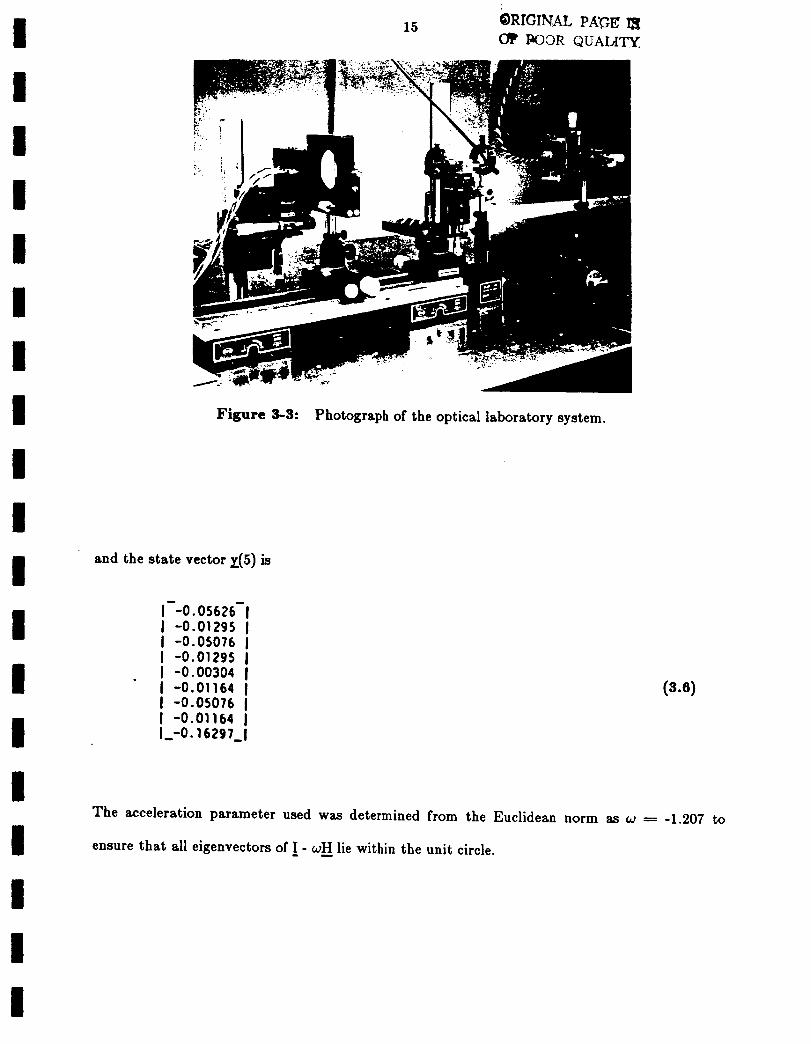
optical laboratory system is shown in Fig. 3-3. It presently occupies approximately 3 feet by 2
feet on an optical bench, however this size can clearly be reduced.
3.3 Number Representation and Electronic Support
This architecture is unique since it can operate analog or to high accuracy. In the analog
mode, the system is linear to 9 bits. This is achieved by correcting for all static errors in the
system. All such errors are correctable as we have noted in earlier publications. The linear
analog performance of the system is presently limited by detector noise, electronic temporal
!

12
i
I
II
I
IIl
ll
ll
lI
ll
coupling, and temporal drift. To operate this system to high accuracy, the data inputs are
encoded and the P1 inputs are fixed while the P2 data moves through the AO cell.
outputs are thus the convolution of the two data bit
performance is obtained by the Digital Multiplication
algorithm 9, 10. To achieve best performance, we operate DMAC with N digits and L levels and
thus achieve L N accuracy. With N _ 10 and L _--- 7, we achieve 28 bit accuracy with only 10
digits or PI point modulators. With 10 modulators per row at P1 and input data at 10 Mhz per
channel, this system performs 20 multiplications and additions per 0.1 _us or 200 MOPs (complex
multiplications and additions).
The P3
streams and hence high accuracy
by Analog Convolution (DMAC)
The electronic support system is quite general purpose and well engineered. A 68,000
control processor running UNIX is used for support. It contains 512K bytes of no-wait memory
and 512K bytes of multibus memory. The system also contains its own 20M byte disk and an
0.5" 1600 BPI tape drive. This support system and processor is thus quite self-contained. It can
be down-loaded with data from a VAX. The input data to P1 and P2 is buffered in the high-
speed parallel memory (12 bits per channel, 8 channels per board, 10 MHz per word per channel).
Separate high speed 12 bit 10 MHz D/As are present on each memory output channel end PI
and P2 input. The system's P3 output data is similarly processed with parallel A/D (12 bit, 20
MI-Iz) and memory boards for each detector output. The general diagram of the digital support
facility is shown in Fig. 3-4. It also includes video terminals, video boards and a display. A
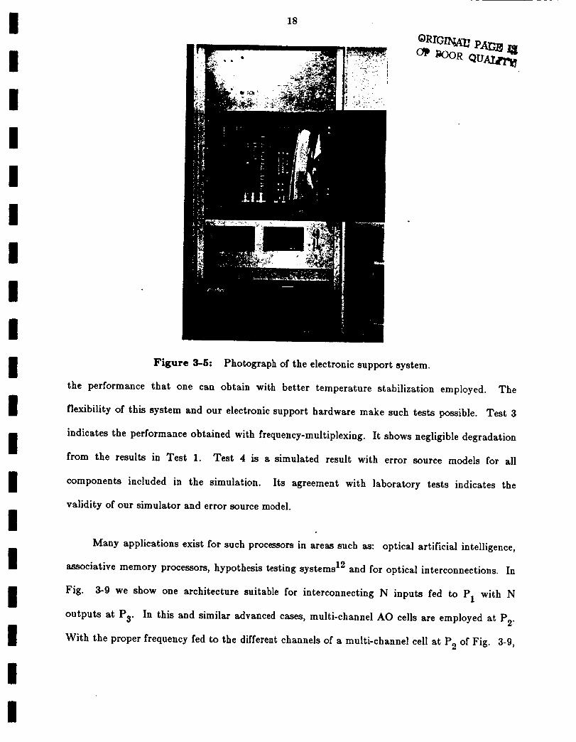
photograph of the electronic support system is shown in Fig. 3-5.
We operate the system to maintain optimum data flow. Another attractive aspect of this
system is its ability to handle matrix and vector problems larger than the size (the number of
point modulators at P1) of the system. One can achieve partitioning of such large problems by
feeding the matrix elements diagonally to PI and partitioning the problem diagonally, with
!

II
II
II
II
III
I
II
II
I
13
subsequent diagonal data flow. In Fig. 3-6, we show an alternative and preferable partitioning
scheme. We consider the multiplication of a nine element vector by a 9 x 9 matrix on a system
with five input point modulators PI" The vector data is fed to the AO cell at P2 and repeated
twice. The five input point modulators at PI are fed with five different matrix elements at
successive time intervals nT B. In Fig 3-6, the matrix elements are labeled with numbers from 0
to 18 denoting the order at which different groups of matrix elements are fed to the P1 laser
diodes. The numbers associated with each group of matrix elements correspond to the time
intervals 1T B to 18T B. The associated system outputs are combined as noted beside the table.
3.4 Case Study and Algorithm
The case study chosen was an optimal control problem, i.e. the calculation of the optimal
controls to minimize a quadratic performance index for a linear quadratic regulator problem.
This involves solution of a nonlinear matrix equation, the algebraic Ricatti equation, for S,
SF + FTs - S G R'IGTs + Q--_ O. (3.1)
We solve this using the Kleinman algorithm
S_(k)F(k) + FT(k)S(k)_----[S(k-1)GR'IG_Ts(k-1) + _. (3.2)
To solve (3.2) for _ we convert (3.2) to a system of linear algebraic equations by
lexicographically ordering the matrix S(k) as the vector x(k). The solution for x thus requires
solution of the linear algebraic equation
H(k)x_(k)---- y(k), (3.3)
for x(k). This is first done for k _--- 1. Then x(1) is used to update and calculate the new
H(k+l). The new Eq. (3.3) with k -_- 2 is then solved for x_(2). And the process is repeated. We
denote the outer (Kleinman) loop step index by k. Using a recursive Richardson solution to (3.3)
for each iteration k (with r being the Richardson index), we solve (3.3) for each k using
x(r+l) _- (I- _H__)x(r) + a_. (3.4)

I
II
II
I
III
II
II
II
III
14QRIGINAL PA'GE 1_1C_ _OOR QUAUn_
10 lASER DIODE _ I
COLLZ_TING PENS INTEGRATING OPTICS b:b [b( )_b(2),b (3) letc HORIZONTAL FOURIER 6 OUTPUT DETECTOR
(PLAME P_) (LENS SYSTEM L.) -- 1 1 l 1 " TRANSFOmdI_C n_VTP¢ DETECTORS POST-
J_OUETO-OPTIC CELL '.... _'_'_" "2 n "
(P_ P2)
Figure 3-1: Simplified schematic of the space integrating optical linear algebra
processor.
SEMICONDUCTOR LASER
7Z8680g
Figure 3-2: Details of one point modulator laser diode and collimating optics system.
The specific problem chosen concerned a F100 turbofan jet engine, an N x N matrix H, and
an N x 1 vector y, with N = 9. The matrix H (5) after the fifth Kleinman loop is
| -0.657 -0.083 0.404 -0.083 0.000 0.000 0.404 0.000 0.000-1I 0.063 -0.470 -0.021 0.000 -0.083 0.000 0.000 0.404 0.000 I| -0.138 -0.087 -0.828 0.000 0.000 -0.083 0.000 0.000 0.404 II 0.063 0.000 0.000 -0.470 -0.083 0.404 -0.021 0.000 0.000 II 0.000 0.063 0.000 0.063 -0.284 -0.021 0.000 -0.021 0.000 II 0.000 0.000 0.063 -0.138 -0.087 -0.642 0.000 0.000 -0.021 II -0.138 0.000 0.000 -0.087 0.000 0.000 -0.828 -0.083 0.404 II 0.000 -0.138 0.000 0.000 -0.087 0.000 0.063 -0.642 -0.021 II__ 0.000 0.000 -0.138 0.000 0.000 -0.087 -0.138 -0.087 -1.000__1
(3.5)
I
I
I
II
II
II
III
II
I
iII
I
15 ¢DRICI_AL PAGE l_
O_ I_OOR QUAHTY
j_ "4
Figure 3-3: Photograph of the optical laboratory system.
and the state vector y(5) is
I--0.05626-1I -0.01295 IJ -0.05076 JI -o.01295 II -o.oo3o4 II -0.01164 II -o.05076 II -0.01164 II_-0.16297_1
(3.6)
The acceleration parameter used was determined from the Euclidean norm as w _ -1.207 to
ensure that all eigenvectors of _I- _I-I lie within the unit circle.

16
I
I
II
III
3.5 Laboratory Results
Figure 3-7 shows the linear analog performance of the system. The three laser diode (LD)
inputs were ramps in time over the 4096 level range allowed by our D/A converters (top figure).
The RF input to the AO cell contained three regions (opposite the three LD inputs respectively)
at 1/6, 1/3 and full power (central figure). The three detector outputs (lower figure) show the
products of the LD ramp input and the three different RF levels. The accuracy measured was 10
bits (0.1_). Due to temperature drift and temporal effects, on-line system performance is
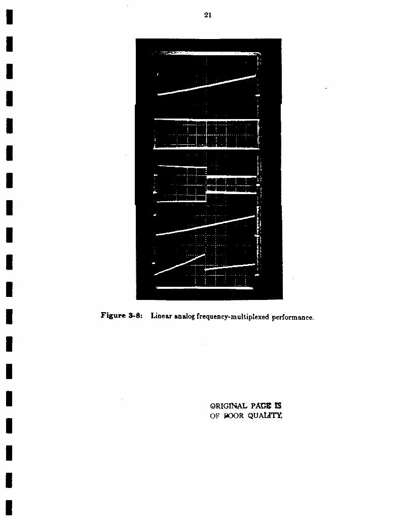
typically nine bits. Figure 3-8 shows the linearity and frequency-multiplexing performance of the
analog system. The laser diode inputs were ramps (top figure). Two multiplexed frequencies to
the AO cell were used and fed with the uniform half strength signal on frequency one (see second
figure) and with a full and one-third power signal present in different regions on frequency two
(see the third figure). Detector output one (see the fourth figure in Fig. 3-8 and detector two
output (see the fifth figure in Fig. 3-8) are the products of a laser diode ramp and the associated
RF signals. This demonstrates the accuracy of the system under frequency-multiplexing. The
two frequencies used here were 175 MI-Iz and 225 MHz. In other tests and demonstrations, the
high accuracy of the system with base two and with higher radices has been demonstrated and
quantified.
Table 3-1 summarizes four of the test results obtained on the system of Fig. 3-1 in the
solution of (3.3) for the F100 problem described in Section 3.4. The performance measures used
were the fractional error z_x in the solution vector and the fractional error in the closed loop
poles z_k. The /t)_ measure is the preferable one, since it describes the regulated control system
we consider. Our goal was to obtain a z_), accurate within 1-2°_. This is quite acceptable and
compatible with the accuracy with which the parameters of such control models are selected.
We include both performance measures to note that larger errors in the computed vector can be
obtained with adequate /tk error resulting. Test 1 is a time-multiplexed version of the system,
!
17
TABLE 3-1:
Laboratory (Tests 1-3) and Simulated (Test 4) data results
Teat
No. Code
Fractional
Error Ax
in Soln. Vector
Fractional Error
in Closed-LoopPoles Ax Remarks
1
2
3
4
LQRL.txt 0.062
LQRMduty.txt 0.048
LQROmux.txt 0.071
VIPAE.txt 0.075
0.014
0.009
0.014
0.023
x.
Reduced LD Drift
Freq.-Multiplexing
Simulation
I
I
II
II
I
-,:.% |jP w_Slg
1r TI , !
ills" "il "_ .oA.o. l =
, IIII | • INTtMFAC[
I I "_°
I _..o.o-,o- J II
l
L_ VIDEO
" IOARDS
t MULTIIUS< _- .E.ORV
{2_IK •Tt*ILI
CONT ftOLLER
,
I !L_ .-I
Figure 3-4: Diagram of the electronic support system
in which bipolar data is accommodated by using a system twice, and subtracting the outputs on
successive cycles. In Test 2, the system was operated at a reduced duty cycle to reduce the
effects of laser diode drift. This test achieved the best accuracy and is also quite indicative of
I
18
otr vr
Figure 3-5: Photograph of the electronic support system.
the performance that one can obtain with better temperature stabilization employed. The
flexibility of this system and our electronic support hardware make such tests possible. Test 3
indicates the performance obtained with frequency-multiplexing. It shows negligible degradation
from the results in Test 1. Test 4 is a simulated result with error source models for all
components included in the simulation. Its agreement with laboratory tests indicates the
validity of our simulator and error source model.
Many applications exist for such processors in areas such as: optical artificial intelligence,
associative memory processors, hypothesis testing systems 12 and for optical interconnections. In
Fig. 3-9 we show one architecture suitable for interconnecting N inputs fed to P1 with N
outputs at P3" In this and similar advanced cases, multi-channel AO cells are employed at P2"
With the proper frequency fed to the different channels of a multi-channel cell at P2 of Fig. 3-9,

II
II
II
I
III
II
II
II
II
I
I0
X T
"Io o 'o o oi Io o "o oi
"_ lo o _o o oi Io o "o
_ o"o oJ lo o, o o o]'_ Io o ,.o oJio o 'o o
o o'o oi Io o-o oJE'
I.t4
2.15
3,1¢
4.17
S. IO
G. IO
?.II
8.12
S. 13
H
FiKure 8-6: Data flow arrangement for partitioning
any of the P1 inputs can be connected to any of the P3 outputs. This architecture of Fig. 3-9 is
due independently to various authors. If all N inputs are the same, then the system can operate
in a broadcasting mode as would be needed for clocking and similar operations. Many useful
architectures and algorithms are thus possible with a basic space integrating frequency-
multiplexed matrix-vector processor, especially when multi-channel AO cells are included. If the
full length of the multi-channel AO cell in Fig. 3-9 is employed, then one can envision using this
dimension of the system to encode data, thus achieving both high performance (number of
multiplications per second) and high accuracy (with advanced encoding techniques).

2O ORrGrNAU P_'CT.
O_ I_OOR QUALITy
Figure 3-7: Linear analog performance of 10 bits (0.1%).
3.6 Summary and Conclusion
We have advanced a new space and frequency-multiplexed architecture for matrix-vector
processing. We have also noted several new partitioning methods for data in such a processor.
The on-line electronic support system for such a flexible (analog and high-accuracy) optical linear
algebra processor has been detailed and demonstrated. The major accomplishment has been the
demonstration of the solution of a real world problem on such an optical matrix-vector
processor.
II
II
II
II
III
II
I
II
II
I
Figure 3-8:
21
Linear analog frequency-multiplexed performance.
ORIGrI_AL PA_E _
OF _OOR QU_

i 22
i ,N,IN 2
!
Ii
II
!II
I
II
II
|i
FREQ SELECTIONINPUTS -"- A0
Figure 3-9:
P$
C
DD _ OUT.
DETECTORS
Frequency-multiplexed optical interconnection
architecture.
OUT I

23
4. REAL-TIME OPTICAL LABORATORY
LINEAR ALGEBRA SOLUTION OF PARTIAL
DIFFERENTIAL EQUATIONS
i
I
I
II
IiI
I
I
II
Il
4.1 Introduction
A Space Integrating (SI) Optical Linear Algebra Processor (OLAP) employing space and
frequency-multiplexing, new partitioning and data flow, and achieving high accuracy
performance with a non base-2 number system is described. Laboratory data on the performance
of this system and the solution of parabolic Partial Differential Equations (PDEs) is provided. A
multi-processor OLAP system is also described for the first time. It use in the solution of
multiple banded matrices that frequently arise is then discussed. The utility and flexibility of
this processor compared to digital systolic architectures should be apparent.
Many OLAPs have been suggested 7, but few have been fabricated and limited laboratory
use of these systems in the solution of practical engineering problems has been presented 13' 14
In Section 4.2, we review one well-engineered OLAP architecture and discuss its laboratory
fabrication, its electronic support system and its performance. In Section 4.3, we discuss several
features and uses of the system to demonstrate its versatility. Our case study and the algorithm
are then detailed in Sections 4.4 and 4.5. Optical realization issues are discussed in Section 4.6
and laboratory results are then advanced in Section 4.7.
4.20lap Architecture and Fabrication
The OLAP we consider is shown in Figure 4-1. Plane P1 is imaged onto P2 and the output
light leaving P2 is space integrated onto P3" Multiple linear point modulator arrays at P1 are
used to allow bipolar (using two linear PI arrays) and complex-valued (using three linear PI
arrays) data to be processed. Frequency-multiplexing at P2 (using two or three frequencies) is
used to achieve bipolar and complex-valued P2 data. The input P1 vector data multiplies the
i

I
II
II
II
II
III
II
II
24
multiple vector data at P2 and the Vector Inner Product (VIP) outputs appear on separate
horizontal detectors at P3" The VIPs of different input P1 data appear at different vertical
locations in P3" This space and frequency multiplexed SI OLAP employs local and global
interconnections.
The system is fabricated using Laser Diodes (LDs) with individual collimating optics for
each P1 point modulator and a TeO 2 Aconsto Optic (AO) cell at P2 with a T A -_- 1 ps aperture
time, a bandwidth BW A = 200 MHz and a center frequency fc -----200 MHz. Three output P3
detectors are fiber optically coupled to Selfoc lenses in the detector plane to accommodate
adequate spacing of detectors. We denote the temporal separation between data packets in P2
(the different P2 regions illuminated by different P1 point modulators) by T B. At 10 MHz
operation (T B -----0.1 ks), the present system supports N ----- 10 point modulators and achieves
200 MOPs (millions of operations per second, where an operation is a complex-valued
multiplication and addition). The present laboratory data is taken with a 4 MHz data rate per
channel (T B -_- 250 ns) on a system using 5 input LDs at PI"
The electronic support system for this processor was detailed elsewhere 5. It includes
parallel high-speed memory channels with 12 parallel output bits per channel each at 10 MHz.
Each parallel output memory channel is fed to a D/A and to one of the P1 and P2 inputs. The
P3 detector outputs are fed through parallel A/Ds to parallel input memory channels. The entire
system is under control of an 68,000-based microprocessor with tape, disc, terminal, monitor, etc.
and with a VAX port. The entire system is thus quite self-contained and well-engineered. This
is essential to allow quantitative data to be obtained and to guide future research and OLAP
design.
|
III
I
III
II
II
II
II
I
II
2.5
10 _R DIODE _ IMAGING AND bOU'J'PLPr _ DLPI_C'rOR
CDI.LZMATZNG PENS IN'IT.GRATZNG OPTZCS b:b I It_:l).b(_).b:$),et¢. HOR17J014ff/_ t:Ot_IE. DETECTORS POST -
TI_NSFOP_qING OPTICS (pLANE P$) P_ING(P[JM_ PI ) (LENS SY_ L 1) I_U_X"DIICY-I_LTIPrJ'XI_D (LI_S SYST_ /-2)
_z¢ CIZZ.L
(i_JU_ P2)
Figure 4-1: Simplified schematic of the space integrating optical linear algebra processor.
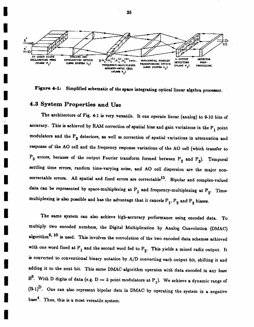
4.3 System Properties and Use
The architecture of Fig. 4-1 is very versatile. It can operate linear (analog) to 9-10 bits of
accuracy. This is achieved by RAM correction of spatial bias and gain variations in the P1 point
modulators and the P3 detectors, as well as correction of spatial variations in attenuation and
response of the AO cell and the frequency response variations of the AO cell (which transfer to
P3 errors, because of the output Fourier transform formed between P2 and P3)" Temporal
settling time errors, random time-varying noise, and AO cell dispersion are the major non-
correctable errors. All spatial and fixed errors are correctable 15. Bipolar and complex-valued
data can be represented by space-multiplexing at P1 and frequency-multiplexing at P2" Time-
multiplexing is also possible and has the advantage that it cancels PI' P2 and P3 biases.
The same system can also achieve high-accuracy performance using encoded data. To
multiply two encoded numbers, the Digital Multiplication by Analog Convolution (DMAC)
algorithm 9, 10 is used. This involves the convolution of the two encoded data schemes achieved
with one word fixed at P1 and the second word fed to P2" This yields a mixed radix output. It
is converted to conventional binary notation by A/D converting each output bit, shifting it and
adding it to the next bit. This same DMAC algorithm operates with data encoded in any base
B 6. With D digits of data (e.g. D -----5 point modulators at P1)" We achieve a dynamic range of
(13-1)D. One can also represent bipolar data in DMAC by operating the system in a negative
base 4. Thus, this is a most versatile system.
I

26
I
I
I
I
I
I
Many data flow and partitioning methods are possible on this system. Consider a matrix-
vector multiplication. One can feed the matrix diagonals time-history to different P1 point
modulators and the vector data to the AO cell. This allows partitioning along the matrix
diagonals and is quite suitable for banded matrices. When the vector is longer than the AO
cell's number of data slots, only part of the vector is present in P2 at any T B and a different
part of the vector is present in each T B. During each TB, the associated N elements of the
matrix are easily determined and fed in parallel to P1 (N elements each TB )13. This is the
partitioning method we used in our earlier demonstration of the use of this system in the
solution of nonlinear matrix equations, specifically the algebraic Rieatti equation 13. For
matrices with multiple bands (e.g. banded matrices in which one band is separated from the
other by many elements, as arises in PDEs), the non-zero matrix elements on each row can be
fed to P2 and repeated with the associated required vector elements easily determined and fed in
parallel to P1 each T B. This method will be used in our PDE case study. Another new
partitioning method that improves throughput involves feeding successive encoded numbers to
P2 on separate frequencies time-multiplexed. This avoids dead time in loading and unloading the
AO cell and improves performance by a factor of 1.8. This frequency-multiplexed operation is
included in our laboratory experimental data results.
4.4 Problem Definition
We consider the solution of a parabolic PDE on an analog and a high-accuracy version of
the same OLAP laboratory system. The specific parabolic PDE selected is the transient
diffusion equation with two spatial variables plus time,
ut = + u), (4.1)
where subscripts denote partial derivatives with respect to time, x, or y (e.g. Uxx denotes the
second partial derivative). The objective is to determine the temperature distribution u as a
function of space (x,y) and time t. We consider the case when the thermal diffusivity _ is
|

27
constant, which is typical of an isotropic time-variant medium. The extension to the non-
isotropic case is straightforward with a becoming a function of the spatial coordinates (x,y).
The temporal evolving nature of the problem with time requires solutions u(x,y,tn) at different
time instances to be used to calculated the solution u(x,y,tn+l) at the next time instant. The
two types of problem formulations and solutions are explicit matrix-vector (M-V) and implicit
LAE (Linear Algebraic Equation) formulations. Both begin with a finite difference solution to
(4.1) with a forward difference (forward Euler) approximation of u t as
(u i+l- ue, )/at,
where n is the time index and (i,j) are the space indices, i.e.
Ax, z_y and At are the space and time step sizes used.
u_j+1 is u[iAx,jAy,(n+l)Zit], where
At each spatial location (i,j), the
temperature at successivetimes n and n+l are calculatedand differencedto produce ut.
I
I
I
II
Ii
In the explicit solution, we approximate Uxx by a double central difference in x (index i)
Uxx = [un+l,j- 2u_,j + unl,j ]/(z_x) 2. (4.2)
A similar approximation is made for Uyy.
4.4.1 Explicit 1-D M-V Solution
For the 1-D problem
U t _ C_Uxx ,
this yields
un+l= XUn+l + (1-2X)u n + kun I ,
where
)`_- , at/Cz x)2.
(4.3)
(4.4)
(4.5)
This shows that the temperature at time step n+l appears explicitly on the left hand side in
terms of constants and spatial solutions at the prior time steps n. If we denote the spatial
solutions for all i at time n by un then a M-V description of (4.4) results:
un+l = A u_n, (4.6)
where the matrix A has (1-2),)for allmain diagonalelements and ),for elements of the diagonals
above and below the main diagonal,
I
I
III
I
III
II
II
II
II
II
m
),
28
X
(1-2X)
k
X
0-2X)
X (4.7)
* * X
_ X (1-2X)
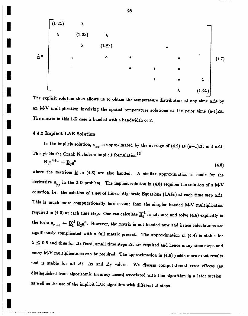
The explicit solution thus allows us to obtain the temperature distribution at any time nat by
an M-V multiplication involving the spatial temperature solutions at the prior time (n-1)At.
The matrix in this 1-D case is banded with a bandwidth of 3.
4.4.2 Implicit LAE Solution
In the implicit solution, uxx
This yields the Crank Nicholson implicit formulation 16
B_:_n+1= B2___
is approximated by the average of (4.2) at (n+l)At and nat.
(4.8)
is made for thewhere the matrices B in (4.8) are also banded. A similar approximation
derivative Uyy in the 2-D problem. The implicit solution in (4.8) requires the solution of a M-V
equation, i.e. the solution of a set of Linear Algebraic Equations (LAEs) at each time step nat.
This is much more computationally burdensome than the simpler banded M-V multiplication
required in (4.6) at each time step. One can calculate Bll in advance and solve (4.8) explicitly in
the form Un+l _--- Bll B_2un. However, the matrix is not banded now and hence calculations are
significantly complicated with a full matrix present. The approximation in (4.4) is stable for
X < 0.5 and thus for Ax fixed, small time steps At are required and hence many time steps and
many M-V multiplications can be required. The approximation in (4.8) yields more exact results
and is stable for all At, Ax and Ay values. We discuss computational error effects (as
distinguished from algorithmic accuracy issues) associated with this algorithm in a later section,
as well as the use of the implicit LAE algorithm with different A steps.

29
4.4.3 Explicit Matrix-Vector 2-D Solution
For the explicit solution to the 2-D problem in (4.1), the finite difference approximation
yields
un+l kun.+l-_ k_,j.l+ (1-4klu_j. (4.9)',1 = _,Un+l,f Xunl, j -'F ,j
To obtain a M-V problem 17' 18, we order the N 2 elements of uij into an N 2 vector _u _---
[Ull,...,UNN] T. With Ax -_ Ziy, this yields the M-V explicit solution of the form of (4.6) with
the matrix A having the central three diagonal elements non-zero and two other non-zero
diagonals N-1 elements away from the main diagonal. With other high-order difference
approximations, more non-zero diagonals 2N-1 away from the main diagonal result. We do not
consider such cases, since the resultant problem presently under consideration suffices and can be
generalized to other problems as they arise.
If we renumber the grid point elements, the bandwidth of the matrix will decrease, however
algorithms to renumber nodes are quite time-consuming. Our proposed multi-processor and
other architectures are appropriate for the simplest node numbering method employed. The
form of the 2-D implicit solution is the same as in (4.8) with the same double-banded matrix
structure existing as occurred in the explicit solution of an LAE required at each time step. The
need to utilize and preserve the banded nature of the matrix now becomes of more concern. If a
direct LAE solution were used, all central 2n÷l diagonals would fill in and become non-zero.
This significantly increases the number of matrix multiplications required and the size of each.
If iterative LAE solutions are used, the number of iterations required (each involving a M-V
multiplication) is difficult to calculate, although estimates of it are possible 19. For an implicit
solution, an iterative LAE solution is preferable, in general. Thus, for these reasons, the explicit
solution in (4.8) and (4.9) was chosen for implementation on our laboratory system. The
boundary conditions for the matrix must still be included in our problem formulation. This is
detailed in Section 4.6. However, the general matrix structure and the size of the matrix is as

3O
described above (i.e. an N 2 x N 2 matrix A with multiple bands separated by N elements and
with N 2 vectors u).
i
I
II
II
II
4.5 Case Study
The case study chosen was the solution of the 2-D diffusion equation for a 10 x 10 cm 2
square aluminum plate with thermal diffusivity a -_- 0.8{} cm2/sec for the case when the plate is
divided into a uniform grid of N x N _ 11 x 11 -----121 _-_ N 2 square elements each 1.0 x 1.0 cm 2
(i.e. Ax _ Ay _ 1.0 cm) and with boundary conditions of zero temperature for the 40
boundary points on the edges of the plate. To satisfy k _ 0.5, we require time steps At _ 0.29
sec. At each time step, we calculate u(x,y,t) at the 81 interior points on the grid. We used a
natural ordering of the grid points on the 2-D plate from left-to-right and top-to-bottom (e.g.
u12 _--- ui, j is the first interior element in the second row). The matrix in our 2-D problem is N 2
x N 2 -_- 121 x 121. We note that 4N-4 of the rows of this matrix are altered by the boundary
conditions associated with the 4N-4 edge elements. The full matrix consists of N x N blocks
each with N x N elements (see Fig. 4-2). The top left block and bottom right block are the
identity matrix I, since the first and last rows of grid elements are edge elements always clamped
to zero temperature (i.e. un _ u_n+l for these elements). The remaining elements in these rows
are zero. The structure for the other diagonal blocks are all similar. They are all tri-diagonal
except for the first and last rows of each block which are zero except for a "1" on the diagonal.
All other elements of these rows are zero. The blocks removed by one element from the main
diagonal have k along the diagonal (except for the rows noted above). The remaining elements of
the matrix are zero.
Our case study thus involves the solution of
u_ = h u_ (4.10)
where u is a N 2 vector and the matrix A is an N 2 x N 2 matrix as shown in Fig. 4-2, with
X = _At/(Ax) 2, ff _--- 1-4X (4.11)
I
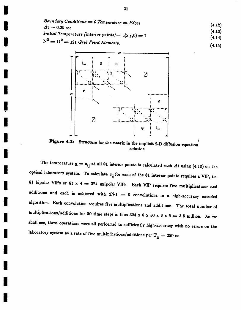
i 31
Boundar_i Conditions _ 0 Temperature on Edges
J At -----0.29 sec
Initial Temperature (interior points}---_ u(x,y,O) _---1
I N 2 _- 112 _--- 121 Grid Point Elements.
I
Figure 4-2:
i
Ii
II
I
.. it-.
I_ 0 O
%-; ........ ;/.; %-....... -e-._i; ......... ,..e_ :L,L :OL e!_...
•. : •. ,1 •.. :",o. _w L: ,o,
• e_e • t ,e • e_
o
............ ]-_
0
0
eo
• I i
.... L ........... A ............ • ...........
IO • I_l • I'e • •
, . :,L,, : •• I ii " i e I Ii e
'e ee.e el.e ee
0 I_
Structure for the matrix in the implicit 2-D diffusion equationsolution
I
I
(4.12)(4.13)(4.14)
(4.1,5)
The temperature u = uij at all 81 interior points is calculated each At using (4.10) on the
optical laboratory system• To calculate uij for each of the 81 interior points requires a VIP, i.e.
II
I
81 bipolar VIPs or 81 x 4 = 324 unipolar VIPs. Each VIP requires five multiplications and
additions and each is achieved with 2N-1 ----- 9 convolutions in a high-accuracy encoded
algorithm. Each convolution requires five multiplications and additions. The total number of
multiplications/additions for 50 time steps is thus 324 x 5 x 50 x 9 x 5 = 3.6 million• As we
shall see, these operations were all performed to sufficiently high-accuracy with no errors on the
I laboratory system at a rate of five multiplications/additions per T B -_ 250 ns.
I|

32
4.6 Optical Realization Issues
4.6.1 Node Numbering
We retain the conventional grid point numbering to allow different solutions and boundary
conditions to be considered, rather than requiring new optimum node numbering techniques for
each problem. A considerable amount of effort can arise in the node numbering phase of
problem formulation and to avoid this and to concentrate on problem solutions, we consider only
conventional left-to-right and top-to-bottom node numbering. In general, this results in the
central diagonal block matrices being diagonal (their bandwidth equals 3 in our case) with other
non-zero elements being separated from the main diagonal by ±(N÷I) elements. For higher-
order differencing schemes, other non-zero elements and block diagonal matrices will exist at 2N
etc. elements from the main diagonal.
I
I
II
I
II
4.6.2 Partitioning and Data Flow
These issues address how the matrix and vector data is fed to the P1 and P2 data planes of
the system and how the P3 processing required to obtain the final desired output is obtained.
Fig. 4-3 shows the three processor scheme with the non-zero matrix diagonal time-history fed to
P1 and delayed versions of u fed to subsequent processors. In general, each P1 data plane
requires M point modulators where M is the largest bandwidth for any block matrix (this is 3 in
our case), the number of processor equals the number of block matrix bands (3 in our case), and
the delays are as shown in the figure. These delays arise because there are many non-zero
elements between and separating the different bands of the matrix (in our case, these bands are
separated by approximately N grid points). The P3 outputs are then the desired N 2 elements of
the temperature vector u at each nat time step.
A multiple banded matrix problem can also be solved on a single processor with the matrix
fed to P1 and the vector u fed to P2" However, this requires that the number of PI point
I

33
U
I
I
I.
l
III
il
Il
I
III
!
11tJ A - (N-I)T B A - NTB
Figure 4-3: Multi-processor architecture for multiple banded matrices
modulators equal the total number of non-zero matrix diagonals. The number of time slots used
in the AO cell also equL! this. This is only 5 rather than 3 for our present case, however in other
problems this number will be considerably larger. However, the AO cell must now support
2N+1 time increments of the vector data and the associated TA _ (2N+I)T B length of the AO
cell is not attractive and is wasteful of the AO cell's TBWP A. This requirement arises because
at any instant, the five point modulators at P1 must interact with the associated u_ elements n,
N-t-n, (N-t-l)-I-n, (N-i-2)-i-n, and (2N-i-1)-I-n along the AO cell. This arises since the 3 matrix
bands are separated by N-2 elements for a grid with N points in 1-D.
An alternate and preferable single processor data flow arrangement (and the one we
implemented in our laboratory system) involves feeding the matrix elements to the AO cell at P2
and the temperature vector data u n to the P1 point modulators. This still requires only five P1
point modulators and now an AO cell with only T A -_ 5T B length. The five matrix elements
and present in the AO cell are always the same (X,)_, 1-4k, X, )_) and this five elements problem
is cyclically repeated continuously. The five PI point modulators are fed with the associated u_n
. n+l (the first interior element), the implicit algorithm inelements u.n.l,jrequired. To calculate u2, 2
(4.9) requires the five u n input elements shown below:
un+l n )ku_,2 (1.4X)u_,2 )_u),3 n2,2 _--- )_u2,1 _" _ ÷ _ XUl,2"
The general ordering of the five u_n elements required at P1
(4.16)
at each T B follows from the
m

34
i
I
i
I
ii!
I
II
I
II
I
regularity of the pattern in (4.16) for subsequent interior elements. These PI point modulators
to which the five u._n elements are fed is orchestrated in conjunction with the movement of the
five matrix elements through the AO cell. It is easy to show that these arrangement achieves an
entire set of N 2 x N 2 temperature updates u(x,y) at a given time in (N-2)2+(M-1) computational
intervals T B. This is the minimum number of non-zero multiplications possible, where N is the
number of points in 1-D in the grid and N-2 is the number of non-zero interior points in l-D, and
M is the number of non-zero diagonals in 1-D in the matrix. The second (N-l) term is the start-
up interval to first load the AO cell and it is negligible• Figure 4-4 shows the input data
sequence for calculation of the second row of interior elements u2, 2 to u2, 9 at time (k+l)At.
tJD's /lO lffaaA u_s
(1,! till 1.,! (kl (hi 0• • • ut6 u_ u_ u_. 4 u3_
|11 "|kll//k_ll " ('kl Ikl
"' """' "" '"' _0
• "-" ""/"'" "" "!!'"',"'" "'"' "", [3UL_ u_l_I u34 u13
t._" _t., t.,
"n uL'S 'YeS v23 ul_, 0
1-4X
-7-IsJS/S $ _ (llroIJ |kgJJ dlk_|J Ike|! (koS) (ll_|p
_1_ ut3 vt_ uL_ u H u_ . . o
J_' I-4_, &' ]k • • •
Figure 4-4: Data sequence for updating of explicit M-V formulation of 2-D diffusion PDE
4.6.3 Partitioning
For cases when the number of non-zero diagonals exceeds the number of PI point
modulators, we can extend the diagonal partitioning to subsequent time steps on one processor
and can assemble the results appropriately delayed at P3 is detailed elsewhere 6. The data flow
in Fig. 4-4 can similarly be partitioned.
I
35
I
I
I
II
II
II
II
II
lI
lI
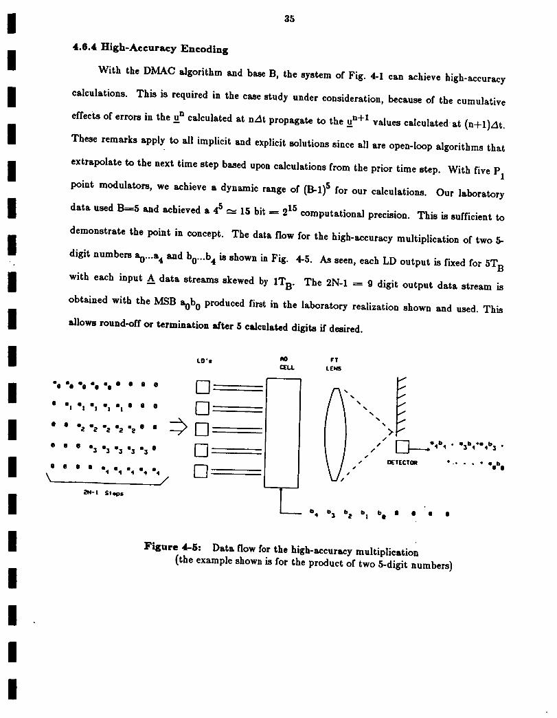
4.8.4 High-Accuracy Encoding
With the DMAC algorithm and base B, the •y•tem of Fig. 4-1 can achieve high-accuracy
calculations. This i• required in the ease study under consideration, because of the cumulative
effects of errors in the u_n calculated at nat propagate to the u_n+l value• calculated at (n+l)At.
These remark• apply to all implicit and explicit solutions •ince all are open-loop algorithms that
extrapolate to the next time step based upon calculation• from the prior time step. With five P1
point modulators, we achieve a dynamic range of (B-l) 5 for our calculations. Our laboratory
data used B-_-5 and achieved a 45 "-- 15 bit -----215 computational precision. This is •ufficient to
demonstrate the point in concept. The data flow for the high-accuracy multiplication of two 5-
digit numbers s0...a 4 sad b0...b 4 is shown in Fig. 4-5. As seen, each LD output is fixed for 5T B
with each input A data stream• •kewed by 1T B. The 2N-1 _-- 9 digit output data stream is
obtained with the MSB s0b 0 produced first in the laboratory realization shown and used. This
allows round-off or termination after 5 calculated digits if desired.
LO'sC_I.L
e 0 • s • 0 an0 • 0 • 0 • • J--J
(J • I • I a I I I • I O • • D
' O "_ "2 -2 -_ -_ O ' _ J _
• 0 • • 3 • 3 m3 • 3 • 3 O
I O • • 0 4 0 4 14 0 4 0 4 [-_
\ /_-! Steps
I:T
LrNS
%%%
," O(TECTOR • •"
b 4 0 3 b_ b I b 0 II • e •
• . * led O
Figure 4-5: Data flow for the high-accuracy multiplication
(the example •hown is for the product of two 5-digit numbers)
I

36
4.6.5 High-Accuracy Data Flow and Partitioning
To simplify data flow and to reduce the number of high-accuracy multiplications required
to a minimum, we calculated )_un and __n ____(1.4k)u n for the entire N 2 vector u.n and in P3
software we assembled the elements uij of u_n+l using (4.9). This reduced the number of high-
accuracy multiplications required to the minimum number possible 2(N-2) 2, where the factor of 2
arises due to the two scalar-vector multiplications used __..n and (1-4),)u n. In the laboratory
system, the summations of elements in (4.9) was performed after decoding to radix 2. In a real-
time system, one would form the sum first and then decode to make the post-processing
requirements faster and simpler.
I
I
II
II
II
4.6.6 Performance Measures
To quantify the performance of the laboratory processor, we calculated the exact
temperature distribution after different time steps using single precision 24 bit mantissa floating
point calculations on a VAX and these results were compared to those obtained on the optical
laboratory system. We refer to the digitally calculated results using this method as the ideal
results. The maximum percent error in the temperature calculated at any grid point and the
average percent error calculated over the plate were determined. These are referred to as the
maximum and average error respectively. To pictorially present the results obtained, we
displayed the calculated temperature distribution for the 11 x 11 grid in 2-D on a display with
white being a temperature of 1 and black being temperature of 0, with 10 increments and steps
of 0.1 in the output temperature calculated displayed using different gray levels. Initially, at t
-_- 0, the interior region of the plate is white and the edges are clamped to 0 (or black). The
final steady state temperature of the plate is of course the entire plate being at the edge
boundary temperatures of 0 (i.e. black). This 2-D data display is quite useful during laboratory
runs to insure that the processor is evolving properly.
!
I
I
II
I
II
I[]
3?
4.7 Laboratory Test Results
The laboratory system used had only one input PI LD array and one set of three output
P3 detectors. The explicit M-V solution was run time-multiplexed with the positive and negative
values of the matrix elements fed to the system at separate times and the difference calculated
after detection. This operating mode is attractive since PI' P2 and detector bias effects then
tend to cancel.
Simulations were performed to compare the explicit M-V and implicit LAE methods. All
laboratory data was obtained using only the explicit M-V solution. In the implicit LAE method,
frequency-multiplexing was used to represent the bipolar matrix data and to allow AO cell
frequency dispersion effects to be addressed. Since the initial temperature for the interior of the
plate was set to 1 (the largest number allowed in the processor), and since the final steady state
temperature across the plate was a uniform value of 0 (the lowest number allowed), no data
scaling was required and the temperature vector u was unipolar. Thus, the only bipolar data
representation of concern was the matrix, not the vector element. In the iterative Richardson
algorithm solution used in the implicit LAE method, the acceleration parameter chosen was 0.5.
After 10 iterations, the iterative solution error was below the computational errors of the
processor. Thus, a fixed number of iterations (10 iterations) and an acceleration factor (w _ 0.5}
were used in the implicit LAE algorithm simulations. In both algorithms, the matrix data was
fed to the AO cell and was recycled as detailed earlier.
4.7.1 Implicit vs. Explicit Solutions with Computational/System Errors Included
The implicit solution is more accurate than the explicit one, because it better approximates
the derivative (not because the LAE rather than the M-V algorithm is better). After 20 time
steps (5.81 secs), the temperature in the center of the plate was estimated to be 0.5803 by the
explicit algorithm, whereas the implicit algorithm yielded a value of 0.5907. The exact value 20
38
was 0.593,as obtained from a closed-formsolution.Thus, the implicitsolutionwas found to be
more accurate than the explicitone. In our simulations,we alsoincluded variouserror sources
that can typicallybe expected in an opticalsystolicrealization.When such error sources are
present,we consistentlyfound (from over 20 differentsimulation runs) that the implicitLAE
solutionwas worse than the explicitM-V one by a factorof 1.4 to 2. This isconsistentwith a
separate theoreticalanalysisindicatingthat noise effectswill add as the mean square value.
Specifically,for noise-likeerrorsin the iterativeRichardson algorithm,even when the iterative
LAE solutionwas run untilthe algorithm errorswere below the hardware computational system
errors,the Richardson portion of the implicitalgorithm was found to add a factorof (2)I/2 _-_
1.4 to the noise growth effectsof the evolving algorithm. Thus, when system and component
errorsare included,the explicitalgorithm appears to be preferable(both theoreticallyand from
laboratorysimulations).
I
I
I
I
I
I
4.7.2 Implicit Algorithm with Variable Time Step Size
The prior comparisons of the implicit and explicit algorithms used the same At time step
in both cases, with the choice being made based upon the stability (k _ 0.5) of the explicit
algorithm. The time step At in the implicit algorithm can be adjusted and with larger At steps,
fewer iterations will be required and hence the algorithm error would be less. However, when
computational errors (such as processor and system accuracy) are included, this tradeoff is not
obvious. If the computational errors are large, coarse time steps should improve performance,
however with smaller computational errors (as we expect in our system), the algorithmic error
can be less with smaller time steps. In tests with a modest amount of system error included in
simulations, we found that doubling the time step to 2Lit yielded an implicit algorithm average
error that was only 60_ of the value obtained with a time step of /it. For larger amounts of
computational error, the improvement was less (16%), but still was rather consistent and
contributed to polarization errors alone. When the modest computational error case was run
!

39
with a step size of 4z_t, the average error in the implicit ulgorithm was found to be 3.8 times
worse than that when the step size was At. Thus, the use of coarse time steps will not always
improve the performance of the implicit algorithm. However, with the proper At time step
choice, an improvement in performance and optimization is clearly possible.
4.7.3 Analog System Laboratory Performance
The analog performance of the system is listed in Table 4-1. We do not expect accurate
results and thus the purpose of these tests was to quantify and assess different system error
sources. As seen, when the output light from the different laser diode input point modulators
are isolated more (by reducing their crosstalk), performance improved significantly (compare test
2 to that of test 1 results). In all cases, the temperature distribution was calculated for 50 time
steps At. The error always increases with time, because of the evolving nature of the algorithm.
For an analog system, operation beyond 10 time steps yielded unacceptably large errors above
2%.
4.7.4 Encoded High-Accuracy Laboratory System Performance
The performance of the system with different bases for the data (column 2) and other cases
(column 3) is shown in Table 4-2. With 5 input point modulators or digits, operation in base B
yields a dynamic range of (B-l) 5. As tests 3 and 4 show, no errors were obtained after 40 time
steps or 40At of time, when base 3 and 4 operation was employed. The theoretical probability
of error for base 4 operation was theoretically computed by us to be 4.5x10 "7. This represents a
quite considerably attractive error rate for an optical processor. With base 5 and 6 operation,
system noise caused the output data to exceed the separation between levels in the output P3
A/D data. In the base 5 runs, 3 errors occurred during the 50At time steps. In a 50Z_t time
step run, 81 grid points are calculated at each time step and thus as noted earlier, a significant
number (3.6 million) of multiplications and additions were performed in each algorithm. These
operations were performed on the laboratory system with a data rate of 5 multiplications and

II
II
40
TABLE 4-1:
Optical Laboratory Hardware Results:
Explicit 2-D Transient Diffusion Equation Matrix-Vector Solution (Parabolic PDE)
Analog System Performance Results (4 MHz)
TEMPERATURE ERRORS
I
I
III
II
II
I
II
TEST REMARKS
NUMBER
AFTER 1At STEP
max error avg error
AFTER 10At STEPS
max error avg error
Low duty cycle
1 (LD temp 3.24% 1.86% 20.5% 14.5%
stabilized)
low duty cycle2 and reduced 2.1% 0.62% 7.66% 2.41%
LD crosstalk
(alternate LDs)
additions per T B _--- 250 nsec. Higher performance is possible with more elements in the system,
by the use of multi-channel AO cells and with a higher input data rate. The present laboratory
system has defined many of these issues and provided very useful initial laboratory results and
experience.
In test 7, frequency-multiplexing of the vector elements to the AO cell was used with the
matrix elements fixed on the laser diodes. Operation of the frequency-multiplexed system
beyond base 3 was not found to be attractive in the present laboratory system, because of spatial
variations in the actual /tO wave transmitted in the cell at different frequencies. This error
source can be corrected with better transducers in the AO cell.
|
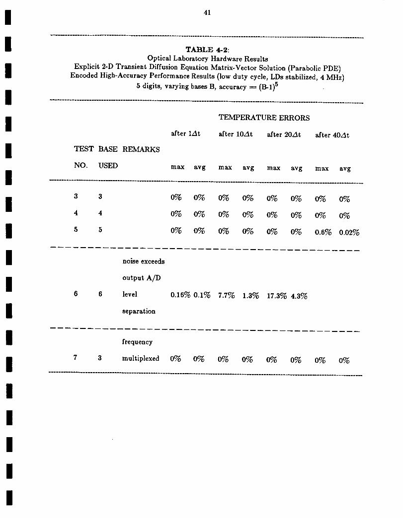
41
TABLE 4-2:
Optical Laboratory Hardware Results
Explicit 2-D Transient Diffusion Equation Matrix-Vector Solution (Parabolic PDE)
Encoded High-Accuracy Performance Results (low duty cycle, LDs stabilized, 4 MHz)
5 digits, varying bases B, accuracy -_- (B-l) 5
TEST BASE REMARKS
NO. USED
after 1At
TEMPERATURE ERRORS
after 10At after 20At after 40At
max avg max avg max avg max avg
3 3 0% 0% 0% 0% 0% 0% 0% 0%
4 4 0% 0% 0% 0% 0% 0% 0% 0%
5 5 0% 0% 0% 0% 0% 0% 0.6% 0.02%
noise exceeds
output A/D
6 6 level 0.16% 0.1% 7.7% 1.3% 17.3% 4.3%
separation
frequency
7 3 multiplexed 0% 0% 0% 0% 0% 0% 0% 0%
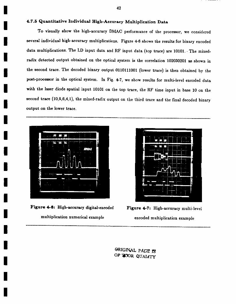
I
I
II
II
II
42
4.7.5 Quantitative Individual High-Accuracy Multiplication Data
To visually show the high-accuracy D_LkC performance of the processor, we considered
several individual high-accuracy multiplications. Figure 4-6 shows the results for binary encoded
data multiplications. The LD input data and RF input data (top trace) are 10101.- The mixed-
raAix detected output obtained on the optical system is the correlation 102030201 as shown in
the second trace. The decoded binary output 0110111001 (lower trace) is then obtained by the
post-processor in the optical system. In Fig. 4-7, we show results for multi-level encoded data
with the laser diode spatial input 10101 on the top trace, the RF time input in base 10 on the
second trace (10,9,6,4,1), the mixed-radix output on the third trace and the final decoded binary
output on the lower trace.
III
II
I
II
II
I
Figure 4-6: High-accuracy digital-encoded Figure 4-7: High-accuracy multi-level
multiplication numerical example encoded multiplication example
@RIGF3gM., P,_G_ I_
Ol_"li:3OR QUALITy

43
Li
I
I
I
I
I
N
4.7.6 Graphical 2-D Temporal Temperature Data Results
In these 2-D spatial representations of the temperature pattern u(x,y) at different time
increments obtained from the optical processor, we employ the coding method earlier (0
temperature _--- black, 1 temperature 1 _ white, gray-scale encoding is used to represent
intermediate temperature values with 0.1 increments being employed). Figure 4-8 shows the
theoretically exact output computed on the VAX to single precision. It shows the temperature
distribution of the plate's evolution with time from its initial conditions toward its steady state
value of 0 temperature across the plate. Figure 4-9 shows the results of our analog computation
using reduced crosstalk effects (test 2 in Table 4-1). Its results are quite accurate and clearly
map the general trend provided from the theoretical results in Figure 4-8. Figure 4-10 shows the
results obtained at different time steps for the case of encoded data in base B _ 4, using 5
channels of the system (i.e. a dynamic range of 35). Figure 4-11 shows the results for the case of
an encoded data high-accuracy computation in base B -_- 3 using 5 channels of the system with
frequency-multiplexing employed on the optical laboratory system to achieve higher throughput
data results. All of these data results were obtained on the laboratory system of Fig. 4-1 (except
for the theoretical data in Fig. 4-8).
!
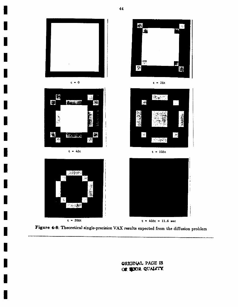
II
II
II
I
III
II
II
II
II
I
44
t = 0 t ffi 2At
t - 4At t = 10At
t = 20At t = 40At = II.6 sec
Figure 4-8: TheoreticM single-precision VAX results expected from the diffusion problem
OR_Ilq_L PAGE _.

II
I
II
II
III
II
II
I
III
I
45
t = 0 (HEX3dutyP.txt) t = 2At
t ,, 4At t = lOAt
t - 20At t = 40At = 11.6 sec
Figure 4-9: Laboratory system results obtained with the analog version of
the processor with reduced temporal and crosstalk effects of P1 included
............... . ...... u .... . ........................ ....o .... . ............................ . ..... N ............... . ...... ...
OF mOOR QUALITY

II
II
II
II
II
II
II
II
II
I
46
t = 0 (B4EX.txt) t = 2At
t = 4At t =lOAt
t = 20At t = 40At = 11.6 sec
Figure 4-10: Optical laboratorytestresultsobtained with base 4
operationwith 5 channelsof the opticalprocessor
QRIG -I_,AEP_GE I__
OF _OOR QUAI_TY

I
II
II
II
II
III
I
II
II
II
47
t = 0 (muxB3.txt) t ffi 2At
t ,, 4At t - lOAt
t = 20At t = 40At = 11.6 sec
Figure 4-11: Optical laboratory system results obtained with base 3 operation
and 5 channels of the optical system employing frequency-multiplexing
.... .._m ...... D ..... . ..... . .... . ................................. . ......................... D ............................
OF_ _ TTY
J
OF I_)OR QUALITy

48
5. TIME AND SPACE INTEGRATING OPTICAL
LABORATORY MATRIX-VECTOR ARRAY
PROCESSOR
L
II
Ii
I
5.1 Introduction
The laboratory realization of a hybrid time and space integrating acousto-optic array
processor is described with the fabrication of the system and its electronic support and a case
study finite element solution on the laboratory system facility emphasized. The output detector
system in this processor is unique and allows the use of different number representations. We
emphasize the use of this system for a new sign-magnitude bipolar data representation that is
quite attractive for use with a new one-channel LU decomposition algorithm and architecture to
solve linear algebraic equations (LAEs). These features are employed in our finite element case
study. This work represents: the first laboratory optical matrix vector multi-channel processor,
the first laboratory realization and demonstration of a new LU decomposition algorithm, the
first laboratory LAE direct solution demonstration, the first finite element method optical
laboratory solution demonstration, a new mixed-radix to binary conversion technique, plus a new
partitioning technique to allow higher accuracy than the number of bit channels permits as well
as system hardware and speed trade-offs. Such optical array processors are of use as linear
algebra processors, associative memory processors, feature extractors for pattern recognition, and
in nearest neighbor classifiers as well as neural networks.
Optical linear algebra processors have received much recent attention 7, but little
laboratory demonstration data 13' 21, 5, 22 In this paper, we advance the first laboratory
realization of a multi-channel matrix vector processor. The basic architecture was previously
described in concept 6. The system architecture is reviewed in Section 5.2. The number
representation used [Section 5.3] and algorithm remarks concerning LU decomposition and
|

49
obtaining higher accuracy than the number of channels allowed by partitioning, plus other
partitioning techniques to solve problems larger than the size of the processor [Section 5.4] are
then addressed. The electronic support requirements are summarized in Section 5.5. The
electronic laboratory support system and laboratory system fabricated are then summarized in
Section 5.6. Our case study is briefly addressed [Section 5.7] and laboratory data obtained is
presented [Section 5.8].
5.2 Architecture Review
The optical laboratory matrix-vector array processor emphasizes the well-known digital
multiplication by analog convolution (DMAC) algorithm 9' 10 The system of Fig. 5-1 uses
detector time integration to achieve this with one encoded data stream fed time-sequentially to
one P1 point modulator and with the second number data representation fed in parallel to AO2
in P2" The P3 detector system performs a shift and add electronically to produce the
convolution of the two input data sequences by time integration and shifting on the detector.
This is attractive, because one output bit of the final mixed-radix product number is produced
each bit time TB_T 1 (the time each Pl modulator is pulsed on). This architecture is attractive
for four major reasons:
1. Both space and time integration are utilized with multi-channel processing.
2. Only one out A/D and adder are required and data flow is ideal.
3. Various number representations are possible on the same architecture.
4. A novel LU decomposition algorithm can be realized on the same optical system.
We denote the number of P1 channels by M and the number of P2 input channels by
N. Each of the M channels produces one high-accuracy product and all M channels produce a
high-accuracy vector inner product (VIP) (with one output bit each TB). Operation of the
system is as follows. Each P1 output uniformly illuminates one row of P2 data. The
convolution of the P1 and P2 data appears time-sequentially at the single-channel P3 output.
This process occurs in parallel for all M input channels to yield an M element VIP output. The
!

!
!
!
II
II
II
III
I,
Dh_C encoding produces this output to high accuracy. New bit data is fed bit serial to AOI ,at
PI' each T I and after r_uF1 of time, one word or encoded number is produced. New data is fed
bit-parallel to AO2 at P2 each T 2 -----NT 1 and a VIP output results each To, with one bit of the
VIP produced at P8 each TI---_T2/N. A full VIP is produced each T 2. In practice; we feed the
second number to P2 twice each T 2 as pulses T 1 long each T2/2 of time. For the general
laboratory w/stem, we employ an M=I0 channel AO cell at P1 and an N--_32 channel AO cell at
P2" For the initial laboratory design, M=I0 and N-_-32. Both A0 celk exist in our laboratories
(AO1 is a point modulator with 100MHz bandwidth and AO2 has an aperture TA-_-5/_s and a
bandwidth of 200 l_-Iz). Both ceils have center frequencies of about 300 ]_,fl-lz.
. RICROPROCESSOR .Q 0
Figure 5-1: Multi-Channel High Accuracy Time and Space
Integrating Architecture 6
I 5.3 Number Representation
I The DMAC algorithm can be applied to any base 6 and such
I
I
techniques represent
considerable speed improvements as well as hardware reductions 6. For example, with N=10
channels at P2 and L--2 levels (Base B--_2), we achieve LNw210=-10 bits of accuracy. However,
with N_10 and B_3 (L_---8), we can realize LN=810-_-30 bits or higher accuracy with no
I
I
I
I
II
II
I
51
reduction in speed or performance. If we reduce N to N-_-6 and still employ B_---3 (L:----8), we can
achieve 86_18 bits of accuracy with fewer channels (N---_6). This reduces hardware as well as
speeding up the multiplication' throughput (VIP multiplication time T2_-NT 1 is also reduced
since N is reduced). The hardware requirements are also reduced (since N---_6 versus 10 channels
of P2 input RF electronics and N_6 versus 10 channels of output P3 detector channels are now
required). This is achieved with an increase in the A/D P3 requirements. Floating point
accuracy 23 is achieved by optically processing the mantissas and with digital processing
performed on the exponents.
Our present case study and application requires only bipolar data. This can be achieved
by use of sign-magnitude 6, 2's complement 1, negative base 4 or by use of biased 24 data
representations. As detailed in the references noted, different number representations are more
suitable for parallel channel architectures in which data is summed on the output detector, than
are other number representations. In the specific case study of concern here, we consider a direct
LU matrix decomposition algorithm 6 which requires only one channel of the system of Fig. 5-1
[see Fig. 5-2 and reference 6]. The system of Fig. 5.1 is attractive since it allows various
encoding schemes to be implemented on the same architecture. We employ different techniques
in different stages and for different uses of the system. We use sign-magnitude number
representation for the LU decomposition algorithm we emphasize here. The other number
representations follow directly and can be used as necessary for a given application. For
complex-value data, the three-tuple or four-tuple number representation is used as required. We
note (as emphasized in other publications 1' 4, 24) that multi-channel processors such as that of
Fig. 5-1 are necessary to achieve the higher number of multiplications per second needed for
optical systems to compete with digital parallel and multiple processor systems.
For the present system, AO2 has an aperture time TA..-_5ps, which we divide into M

II
II
II
O(LAY/
Figure 5-2: One-Channel LU Decomposition Architecture
for Matrix Decomposition 6
regions, i.e. lvIT2_---10T 2 _ 5ps, i.e. T2-----0.Sps. In our general laboratory system, we use
T2_----0.25/_8 (a 4 IVlHz data rate) and feed repeated data (each pulse T 1 long) to AO2 each T2/2
and we feed new bit data to each PI channel each TI=T2/M--0.025ps. The use of two P2
pulses in each T 2 insures that one AO2 data packet is present during one I"2/2 interval. The
TeO 2 longitudinal AO cells used in P1 and P2 satisfy the above requirements. Thus, the system
design allows input PI data to AO2 each Tl_25ns (at 40 MHz) and new P2 data to AO2 each
T2-----MTl_250ns.
I 5.4 Partitioning, LU Decomposition and Accuracy Tradeoffs
I
II
I
8.4.1 Diagonal Partitioning
To allow partitioning of matrices whose size exceeds the number of input P1 elements in
AOI, we partition the matrix along its diagonals 6. In other cases, we feed the proper matrix
data to the PI point modulators each T B as detailed elsewhere 13' 21 We have also detailed a
multi-processor architecture suitable for partitioning of matrices with multiple banded
structure 21.
I
I
I
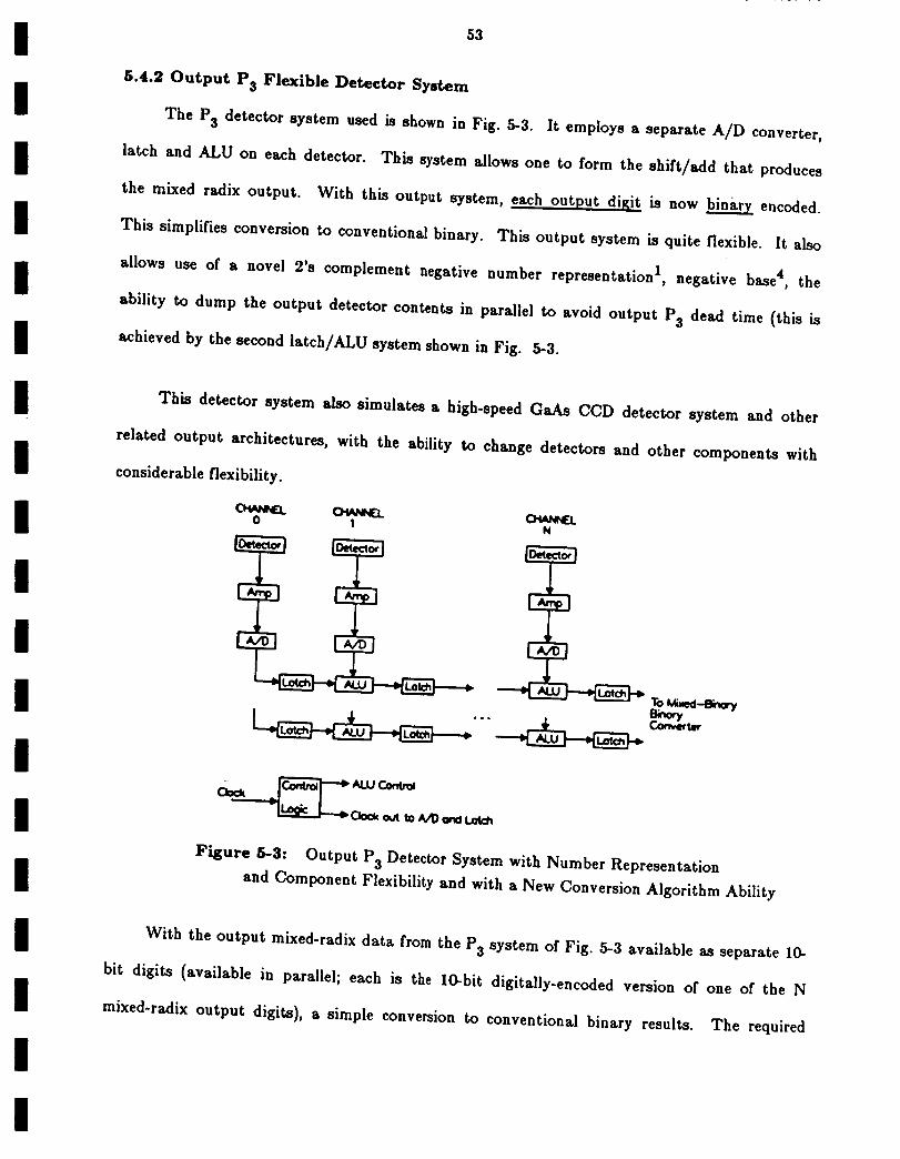
m
l
n
53
II
II
II
III
5.4.2 Output P8 Flexible Detector System
The P3 detector system used is shown in Fig. 5-3. It employs a separate A/D converter,
latch and ALU on each detector. This system allows one to form the shift/add that produces
the mixed radix output. With this output system, each output dil_it is now _ encoded.
This simplifies conversion to conventional binary. This output system is quite flexible. It also
allows use of a novel 2's complement negative number representation 1, negative base 4, the
ability to dump the output detector contents in parallel to avoid output P3 dead time (this is
achieved by the second latch/ALU system shown in Fig. 5-3.
This detector system also simulates a high-speed GaAs CCD detector system and other
related output architectures, with the ability to change detectors and other components with
i
1
m
considerable flexibility.
0
q
I -+ ALtJ_
I Oock o_ t0 _VD or_ t.ot_
II
I
N
p
_m
Figure 6-3: Output P3 Detector System with Number Representation
and Component Flexibility and with a New Conversion Algorithm Ability
With the output mixed-radix data from the P3 system of Fig. 5-3 available as separate 10-
bit digits (available in parallel; each is the 10-bit digitally-encoded version of one of the N
mixed-radix output digits), a simple conversion to conventional binary results. The required
I

I
I
I
I
II
I
II
II
II
I
I
54
circuitry (Fig. 5-4)) is quite simple. The algorithm required is also simple: for the first word
(the binary representation of the least significant digit) we perform no shift and merely input
this digital data to the accumulator at time T1; for the second word, we shift the output data by
one bit (this is achieved in the parallel barrel shifter) and add this shifted Word to the
accumulator at bit time 2TI; the third word is shifted by two bits (in the barrel shifter) and
added to the accumulator contents; etc. Figure 5-5 shows an example of the operations required
and performed (the shift and add of successive output data and the output of one bit of the
result per TI).
(1_7) s.. ? * 21) .. 'Jr - lit
6 " 21 • tO • |Of
$ * 2 :I" 13 8 |I
| * 2 s" 8 II I
I?to IO010t_t -
Mlzed-lilnarr Qperatlon of
ovtput trom umlze4°bznary
S_I_/A44 g,o blns.r 7
Coaver_r
I00101 |Intr|
Output toumo_r7 _trlo
Figure 5-4: Schematic of a Simplified
Output Binary Conversion Hardware
System.
Figure 5-5: Example of Output
data conversion in P3 Output
System.
5.4.3 LU One-Channel Algorithm 6
To solve A x ----- b for x by LU decomposition, we decompose the matrix A into A-_LU
(where L and U_.are lower and upper triangular matrices). This allows us to solve the original
problem by back substitution. The decomposition is achieved by multiplying A_. by N
decomposition matrices Pm (when A is N x N). Synthesis of the decomposition matrix is trivial
and requires only calculation of one column of the prior P_.mA_.m.1 matrix (where Am. 1
I

55
P_.m.lAm_2). The realization of the associated matrix-matrix multiplication PmAm.l required by
the algorithm can be achieved on the one channel system of Fig 5-2 (one channel of the
architecture of Fig 5.1). We consider implementation of this algorithm with an augmented
matrix (with a matrix A augmented with b as one column). This produces: one row of the
matrix U_ and one element of the new U_.xx=b_vector each T 2. These outputs can feed a separate
lower triangular (back substitution) processor as shown in Fig. 5.6. At each T2, the optical
system of Figure 5-2 outputs a new row of the next A m matrix required to calculate one element
of the unique column of the next decomposition matrix Pm as shown in Fig. 5-7. The calculation
of the necessary one column of Pm is straight-forward and is detailed elsewhere 6.
1 Row of U
1 elemenf of new
y=Ux=b
Back
SubstitutionProcessor
one _xelement
Per "1"2
I
I
II
II
II
Figure 5-8: Post Processing (for Back-Substitution Solution) Required Per T 2
New A m matrixone row per T2
Assemble
DecompositionMatrix
New .PmMatrix
Figure 5-7: Post Processing (to Compute New Decomposition Matrix Pro) each T 2
5.4.4 Accuracy Above the Number of Channels by Partitioning
To achieve greater than 2N bit precision on a N bit DMAC processor operating in base 2,
we proceed as follows. We convolve the first N bits of the two numbers and store the results.
We then input the next N bits of the two numbers, convolve the results and accumulate these
I

I
II
II
I
III
III
I
II
II
I
56
and the prior N convolved bits. This procedure repeats for the number of cycles needed. By this
technique (utilized in our laboratory system), we achieve an accuracy above the number of bits
available in the processor. This allows us the added flexibility of a different number of system
bits and final system accuracy (thus allowing a hardware/accuracy and speed trade-off). For the
system fabricated and the example performed, we use an N-_-3 bit system to produce B_21 bit
accuracy. This requires (Bq-N-1) (B/N)TI=(21q-3-1)7TI=(23T1)7=7T2 of time. This fully
utilizes the available capacity of the processor. This is possible and is a unique feature of the
DMAC algorithm (since carries in it do not occur and need not be handled until in the final
mixed radix to binary conversion}.
5.5 General Laboratory Electronic Support System Requirements
The laboratory electronic support system fabricated used an Intel 286/380 system. This
system runs the iRMX86 operating system with support for C, Assembler, PLM and Fortran.
The hardware includes a VAX interface to download data to the processor. Hardware and
support boards and equipment include: an Intel 286//10 single board processor with a 80286 16-
bit microprocessor, an Intel 80287-8 mathematical co-processor for floating point and
trigonometric calculations, one M-byte of one-wait-state RAM memory, a 2-port serial card, an
intelligent disk control card, a tape control card, two cards for memory subsystem control, two
32 M-byte hard disks, a 1.2 M-byte floppy disk, an 0.5 inch tape drive and output display
facilities.
The electronic hardware concept used employs burst processing, in which input data will be
fed to the optical processor at the memory data rates through multiplexors at high data rates
(40 MHz) through a 4 bit 200 MHz D//A for multi-level PI and P2 input data. The data for PI
and P2 will be provided from parallel buffer memories for PI and P2 input data. These data will
feed the optical processor. The P3 output data is collected by 6 bit 100 MHz A//D's through the
I

57
i
II
II
II
II
shift/add array to input buffer memory channels. These buffer memory channels are provided
on other memory boards. Each input and output memory board provides eight channels of 12
bit data at 10 MHz (0.1 /_8) per channel for 96x10-_-960M bits per second per card. With the
eight cards available, we can achieve approximately 8G bit per second data rate generation.
Figure 5-8 shows a block diagram of the full processor and Fig. 5-9 shows a photograph of the
hardware support. Figure 5-10 shows the P3 hardware in Fig. 5-3. Figure 5-11 shows a close-up
of the P3 hardware board.
5.6 Electro-Optical Laboratory System
The optical laboratory system used in the tests reported is shown in Fig. 5-12. Only
M_I channel of the 10 channel AO1 cell at PI was used (since our LU algorithm requires only a
single-processor channel system). Only N_-3 channels of the 32 channel AO2 cell at P2 were
used (to demonstrate the ability of this system to achieve 20 bit accuracy on a 3 bit channel
system using our partitioning algorithm). The laboratory system was operated with P1-_-0.1 ps
and T2---_-(Nq-B-1)T1-----23T 1 to demonstrate high accuracy. For multi-level encoded data tests,
L_3 levels of the 24 levels possible from the input D/A were used. This allows the output D/A
levels used to be adjusted for processor nonlinearities and noise. The output A/Ds were 6 bit
100 MHz units (one per detector as shown in Fig. 5-3).
5.7 Finite Element Case Study
The finite element case study involved the solution of the system of LAEs K__d_ _ p for d_.
The problem chosen was detailed elsewhere 25. Here, K is the N x N stiffness matrix that defines
the structure of the system and the relationships between the finite elements that model the
structure, p is an N x 1 vector that defines the N possible loads or forces on the structure and d
is the desired output N x 1 vector of the displacements (3 per node) produced at the nodes of the
structure described by K_.with the forces described by p applied. The problem considered was an
aluminum plate 61 x 8t x 1" divided into 8 rectangular plate bending finite element regions as
I

58
F_'_'_'L_-_7_ ___.__JDell-tot/ I[Board[- A_L_A____ - _Amplif kits I
I _,,,,, _ m,mo,y /ICo-- ter I boords I P1 1=2 P3 |
I__'..___'_.I ['a_T:;-m_I ---.-_j"_ J_ In_-6_l
lC.k_k8oo,'d I _,__]
- 't_Figure G-8: Block Diagram of the Electronic Support System
/ 4-- Power Supplies
ECL D/A and Shi(t//Add
_.__ Memory Boards and10 MHz AnQIog Rack
Cord Cage Chassis
Disk Chassis
1/'2" Tape drive
Figure 5-9: Photograph of the Electronic Support System
Figure 5-10: Photograph of P3 Hardware
OF _DO_ QUAMT_

I
II
II
II
II
III
I
II
II
I
5g
Figure 5-11: Photograph of P3 Hardware Board
MemoryData _._
i TektronicslOsc|llator J r_
[__e_ OemognifyOptics t_
P1
Horizontal VerticalSlit Slit
To InputMemory
_oetectorI
P3
Figure 5-12: Block Diagram of the Reduced Laboratory System Usedin the Demonstrations Described
shown in Fig. 5-13. The structure has M=15 nodes with D_-3 degrees of freedom
(displacements, etc.) per node for a total of N _ M x D _ 45 degrees of freedom to be described
for the system. The matrix K is 45 x 45. The matrix bandwidth is reduced to 2g by optimal
node numbering. The boundary conditions used involved clamping two edges of the structure
(the nodes denoted by x in Fig. 5-13) with a force applied in the z direction at the bottom right
I

6O
II
II
II
II
II
II
II
node (case l) and at this node and the adjacent edge nodes (ease 2). The elements required in the
d solution vector were the 3 degrees of freedom at the 8 unclamped nodes (24 unknowns). From
calculations, the dynamic range of K was bund to be 105 (17 bits). We estimated that 21 bits of
precision were necessary to solve for d to reasonable accuracy and to allow processing of K to
reasonable accuracy. We achieve 21 bit accuracy on our N_3 bit channel system with a
partitioningtechnique describedearlierusing(B-kN-1)(B/N)T I _---(21q-3-1)(7T1)_---(23TI)7
7T 2 of time, where B_21 isthe number ofbitsdesiredand the N-1 term accounts for the fact
that the convolutionof N bitsis2N-I bitslong. We use T 2 _ 23T I as noted before. Thus, by
of time foreach run) with 3 bitsproduced per T2, we achieve21running the system 7 times (T 2
bit final accuracy.
X Clamped node
0 Free node
f f'_ r_ / x •
Figure 5-13: The Aluminum Plate Finite Element Structure Used for Our Case Study
5.8 Laboratory System Data
The laboratory data of Fig. 5-14 shows the system's ability to accurately process multi-
level data. Trace 3 shows the binary input sequence to AO2 (negative pulses indicate the
presence of a 1). Trace 2 shows the multi-level time sequential input signal to one channel of
AO1 (more negative values on the scope trace are more positive numbers). Trace 3 should be
shifted right by two time slots (the delay required for this data to reach the time aperture region
of AO2 illuminated by the AOI channel used) to time align the plots. The top trace 1 shows the
P3 output obtained. It is the expected product of the AO2 and AOI data, i.e. the AO1 data in
time slots 3, 5, 9 and 10 (the times when the AO2 data is 1 and not 0).
I

I
I
I
I
II
II
I
61
Figure 5-15 shows the system's ability to convolve two digital bit streams and hence
DMAC processing of high accuracy data. The AO1 time-sequential input to one channel was
161,017 or in binary the 21 bit sequence 000100111010011111001. The AO2 input number was 6
or in binary 110. The AO1 input is shown in trace 4 of Fig. 5-15a. The inputs-to the three
channels of AO2 are shown in traces 1 to 3 (they are 011 respectively or the binary version of the
second number to be processed). The output time history on the three detectors at P3 (opposite
the corresponding regions of AO2) are the products of the AO1 time sequence and the AO2 bits
(1 or 0). These results (Fig. 5-15b) are 0 (for detector 1 opposite the AO2 channel with input 0)
and the input 21 bit sequence (for the other 2 detectors).
Figure 5-16 shows the DMAC algorithm example performed on the laboratory system. The
mixed radix output data from the laboratory system is shown in Fig. 5-17a. The digital
representation of each mixed radix digit is produced in the P3 system of Fig. 5-3 and is shown in
the A0 and A1 output waveforms which represent the two binary digit versions of the mixed
radix output (bit-by-bit). The final conventional binary representation of the output obtained
on the laboratory system is shown in Fig. 5-17b.
The results for our two finite element case studies are shown in Figs. 5-18a and 5-18b
respectively. Column 1 lists each of the 24 internal node degrees of freedom to be calculated.
The values calculated to floating point accuracy on a VAX using IMSL algorithms (column 2)
and on our Intel simulator (column 3). This verifies the accuracy of our Intel processor
algorithm. The results calculated to 21 bit accuracy on the digital system (column 4) and on the
optical laboratory system (column 5) also agree. This verifies the intended 21 bit accuracy of
our optical processor in a full engineering problem.
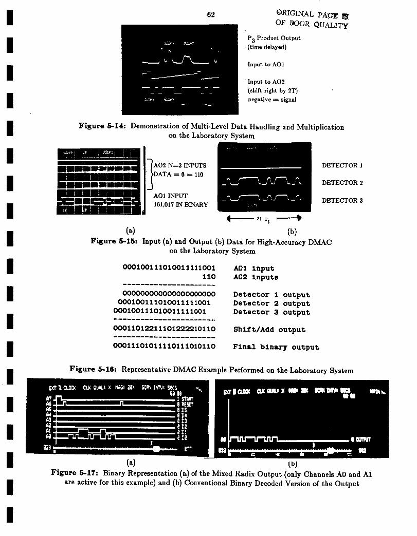
62 ORIGINAL PAGE 1_OF DOOR QUALITy
I P3 Product Output
I
I
I
IlllRIIJglIImlmllbll JDATA = 6 = 110_iinul
(time delayed)
Input to AOI
Input to AO2
(shift right by 2T)negative = signal
Figure 5-14: Demonstration of Multi-Level Data Handling and Multiplication
on the Laboratory System
DETECTOR 1
DETECTOR 2
161,017 IN BINARY DETECTOR 3
• 21 T 1
I (a) (b)Figure 5-15: Input (a) and Output (b) Data for High-Accuracy DMAC
on the Laboratory System
000100111010011111001 AO1 lnput
110 A02 lnputs
Detector 1 output000000000000000000000
000100111010011111001 Detector 2 output
000100111010011111001 Detector 3 output
00011012211101222210110 Shift/Add output
00011101011110111010110 Flnal blnary output
Figure 5-16: Representative DMAC Example Performed on the Laboratory System
1(a) tb)
Figure 5-17: Binary Representation (a) of the Mixed Radix Output (only Channels A0 and A1
are active for this example) and (b) Conventional Binary Decoded Version of the Output
1
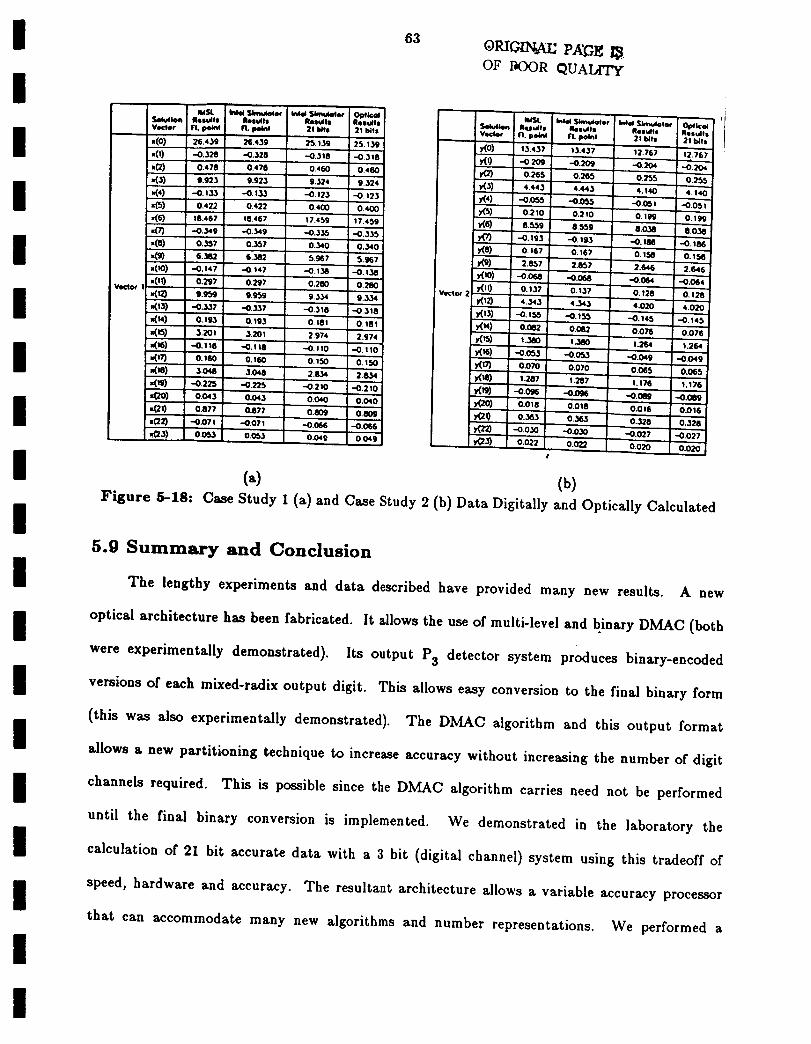
63
OF I OORQUAblTY
IMSLSoivlk_ tletlullllVecter ft. polm
• (0) 26,439
.0) -.o.320• (2) 0.478
•(3) e.s2_N(4) -0.133
x(5) 0.422
1(6) 10.467
=Or) -0.349
• (8) 0,.._7
<g) 6.382
x(lO) -0.147
• (I0 0.297
,_1_) _._7
•(_1 o.193
•(16) -0. I _e
.(17) O. 160
1(18) 3.o_
,_g) .-0.2_
_2o) 0.o4:3
• (21) 0.87;,
u(22) -0.o71
!(23) 0003
Mkd Sl,m_lokw _ $tw_4_o¢Ihlulte ResultsI1. p44nt 21 Idle
26.4.19 2_. 139
-0.326 -0.310
0.476 0.460
9.923 9.324
-,0.133 -0.123
0.422 0.400
18.467 17.4_)g
-0.349 -0.35S
0.357 0.340
6.302 $g67
-0A47 -0.138
0.297 0.280
g.g_g 9.354
-.0.._7 -0.318
0.193 0.181
3.201 2.974
-0.118 -0JlO
0.160 0.1.50
3046 2.634
-0.225 -0.210
0.043 0040
0.877 0.809
-0.071 -0.066
0063 O.04g
Ileeulle S_Io_ II_llult | lileodhl II.lultt Results21 bits VectQr FI. pok'd I1. liel_t 21 bits 21 bite
25139 }_0) 13.437 13.437 12.767 '12.767
-0.3_0 YO) -0._09 -,O.209 --0.204 -0.204
0.460 ),(2) 0.26S 0._5 0._5 O.258
9.324 _3) 4.443 4.443 4.140 4.140
-0,12.1 )(4) -0.0_ -0.0_5 -0.001 -0.051
0.400 y(5) 0.210 0.210 0.199 0.199
17.45g Y(_ 0._5g 8._g 8.0_ 8.038
-0.33.*) y_7) -0.193 -.0. Ig3 -0.186 -0.186
0.340 y{O) O. 167 O. )67 O. 158 O. 158
5.967 y(g) 2.8.57 2.8S7 2.646 2.646
-0.158 ),(Io) -0.o6_ --o.o_ --o.o64 -0.(_0280 v.cto_ 2 y_!t) 0.137 0.137 0.128 0.120
g.3.14 y(l_) 4.34,3 4,343 4.020 4.020
-0.318 y(13) -0.155 -0.155 -0.145 -0.145
O. 181 y{t4) 0.082 0.082 0.076 0.07_
2.974 y(l_) 1.380 IJ80 1.264 1.264
-0.110 )(16) -0.0_3 -0.053 -0.04g , -0o49
O. 150 y(17) 0.0_0 0.070 O.OE5 0.065
2.634 y(18) 1.207 1.207 I. 176 1.176
-0.210 y(19) --0.096 -0.o96 -0.08g --0.0_i
0.040 , ,y(ZO) 0.018 0.018 0.016 0.016
' 0.809 ),,(2O 0.363 0..3E3 0.328 0.328
-0.066 1(22) -0.0.10 -0.030 -0.027 -0.027
0.049 y¢2_ 0.022 0.0_2 0.020 0.020
(a) (b)Figure 5-18: Case Study I (a) and Case Study 2 (b) Data Digitally and Optically Calculated
I
I
I
I
II
I
5.9 Summary and Conclusion
The lengthy experiments and data described have provided many new results. A new
optical architecture has been fabricated. It allows the use of multi-level and b.inary D/vIAC (both
were experimentally demonstrated). Its output P3 detector system produces binary-encoded
versions of each mixed-radix output digit. This allows easy conversion to the final binary form
(this was also experimentally demonstrated). The D_LkC algorithm and this output format
allows a new partitioning technique to increase accuracy without increasing the number of digit
channels required. This is possible since the D_LkC algorithm carries need not be performed
until the final binary conversion is implemented. We demonstrated in the laboratory the
calculation of 21 bit accurate data with a 3 bit (digital channel) system using this tradeoff of
speed, hardware and accuracy. The resultant architecture allows a variable accuracy processor
that can accommodate many new algorithms and number representations. We performed a
I

II
II
II
II
II
II
II
II
II
I
64
laboratory demonstration using a new one-channelLU decomposition algorithm (which, using an
augmented matrix, provides output data for the finalback substitutionstep with perfectdata
flow). We produced the firstlaboratory processing of a finiteelement problem, the first
laboratorydirectLAE solution,and the firstuse of a multi-channelAO laboratorymatrix-vector
system.
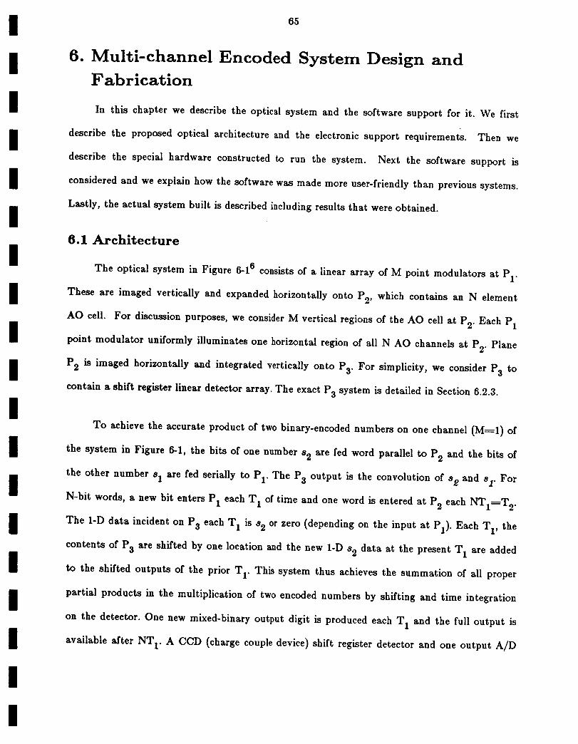
65
6. Multi-channel Encoded System Design and
Fabrication
In this chapter we describe the optical system and the software support for it. We first
describe the proposed optical architecture and the electronic support requirements. Then we
describe the special hardware constructed to run the system. Next the software support is
considered and we explain how the software was made more user-friendly than previous systems.
Lastly, the actual system built is described including results that were obtained.
6.1 Architecture
The optical system in Figure 6-16 consists of a linear array of M point modulators at PI"
These are imaged vertically and expanded horizontally onto P2' which contains an N element
AO cell. For discussion purposes, we consider M vertical regions of the AO cell at P2" Each P1
point modulator uniformly illuminates one horizontal region of all N AO channels at P2" Plane
P2 is imaged horizontally and integrated vertically onto P3" For simplicity, we consider P3 to
contain a shift register linear detector array. The exact P3 system is detailed in Section 6.2.3.
To achieve the accurate product of two binary-encoded numbers on one channel (M-_-I) of
the system in Figure 6-1, the bits of one number s 2 are fed word parallel to P2 and the bits of
the other number 81 are fed serially to PI" The P3 output is the convolution of 82 and s 1. For
N-bit words, a new bit enters P1 each T 1 of time and one word is entered at P2 each NTlwT 2.
The 1-D data incident on P3 each T 1 is s 2 or zero (depending on the input at PI)" Each T1, the
contents of P3 are shifted by one location and the new 1-D 82 data at the present T 1 are added
to the shifted outputs of the prior T 1. This system thus achieves the summation of all proper
partial products in the multiplication of two encoded numbers by shifting and time integration
on the detector. One new mixed-binary output digit is produced each T 1 and the full output is
available after NT 1. A CCD (charge couple device) shift register detector and one output A/D

II
I
I
///
I
e
I
II
II
I
I Figure 6-1: Multi-Channel AO Cell Architecture
I
I
I

Il
II
II
II
II
III
I
II
II
67
converter can achieve the required detection function. We consider the design and electronic
support requirements for a system with M=10 and N=10 in Section 6.2.
6.2 Electronic Support Requirements for Multi-Channel Encoded
System
We now detail the electronic support requirements and capability of the multi-channel
encoded system. For each PI and P2 channel we allow up to three bits (L -----8 levels) of input
data. We allow up to M_---10 channels at P1 and N=10 channels at P2" For multi-channel
algorithms (M>I), we use only L_---3 input levels, since the output A/D on each detector is 6
bits. Section 6.2.3 details these calculations. In this section, we describe the full M=10 and
N=10 system. This allows us to specify the full size and capabilities of the support hardware.
0.2.1 AO Celk and A/D Converters
The electronic support system was designed to support 10 channels of a 32 channel AO cell
at P1 with a center frequency fe=300 MHz and a bandwidth of 100 MHz. This cell is a TeO2,
longitudinal mode device used as a point modulator. The P2 cell is also a TeO 2 longitudinal
mode device with a center frequency fe _--- 400 1VIHz, bandwidth BW A -----200 MI-Iz and length TA
5/_s. Again only ten channels at P2 are considered here. With M=10 and TA_---5/_s , 1V[T2_T A
and T2<0.5/_s. We also require T2=NTI<0.Sps or NTI_---10TI<0.5#s or Tl<0.05#s. The P3
design for Tl=0.05ps is possible. We are presently using T 1 _--- 0.1ps because the high speed
ALU chips necessary for the P3 detector were not available, nor were equipment funds. With
Tl=0.1/_s , we are limited to M_---5 channels in P1 and thus M=5 regions in P2" The P2 channels
are fed with data each T 2. There is a gap between channels on the P1 AO cell that is also equal
to the width of each of the acoustic columns in P1 as shown in Figure 6-2. Because of this, we
feed data to P2 as a pulse of duration T 1 every T2/2 (i.e. 2 pulses T2/2 apart each T2). This
insures that one data pulse is always present in P2 opposite an active region of PI"
i

68
Acousticbeamareas
IGAP
Lighf One channelfrom P1 of P2
T2/2
TT2
Figure 6-2: Diagram of acoustic gaps from PI and data inputs to P2
The number of levels L used per digit and the number of digits N used in the encoding
determines the system accuracy, LN. With L=8 (3 bits) and N_10, we have a dynamic range or
accuracy of 1,073,741,824 (30 bits). With L=3, the accuracy is reduced to 59049 (15 bits). It is
possible to double the dynamic range by simply running the data through the system twice. In
the first cycle the N least significant digits are processed and in the second cycle the N most
significant digits are processed. This method is also used in our laboratory demonstration system
(Section 6.10). This would increase the accuracy on an N_10 channel P2 system to
3,486,784,401 (greater then 31 bi_s). This is expected to be adequate for all initial applications to
be considered. The number of channels M together with L and N determine the A/D
requirements at P3" For the system designed we use an input D/A with 4 bits at 200 MHz. The
data rate satisfies our T 1 data design ( 25 ns or 40 MHz ). For the system design, we use a fi bit
100 MHz A/D in P3" This is fast enough for the 40 ]VIHz P3 shift rate. With this A/D, we can

I
I
I
I
I
III
I
69
allow input values of L--8 for M_-I channels at PI or L_3 for M--10 channels. Section 6.2.3
details the P3 _equirements.
6.2.2 Input Data Requirements
For M=N=10 and TA_-5 #s for the AO cell at P2' we found T 1 <_ 50 ns was required.
We designed the input electronics to allow a T1_25 ns (40 h/_Iz) input data rate and three bits
(eight levels) per T 1 digit. The T 1 rate used in the initial lab system is slower, but this section
considers what the system can provide. This is equivalent to a 40 x 3 = 120 Mbit/sec input
data rate per channel. To achieve this, we plan to multiplex one 12-bit 10 M]-Iz parallel output
channel from our memory boards since its 12 x 10 _--- 120 Mbit/sec data rate is exactly what is
required for one P1 input at 40 MHz and 3 bits. With M=10 channels at PI' we require ten 12-
bit 10 M_Iz buffer memory channels to provide all of the P1 data. The P2 input data rate is one-
fifth that of P1 (one T 1 pulse every T2/2=5T1). We could thus use only two 12-bit 10 MHz
memory channels for all N--_10 channels of P2 data. However, we use 10 channels because it
simplifies timing. With 8 memory channels per memory board, we employ two memory boards
for P1 and two for P2 with a multiplexer planned for each pair of memory boards.
6.2.3 Detector P3 Requirements (future and now)
In the final embodiment of the system in Figure 6-1, the P3 detector system could utilize
an advanced GaAs or VHSIC CCD shift register detector and partitioned A/D converters and
adders. For the near term and in the laboratory system, separate detectors, A/D converters and
adders are employed. If a system with N_M_10 and L-_8 were used with one A/D, the A/D
must resolve 7 x 7 x 10 x 10 _ 4900 _-- 13 bits. For a system with L_---8 (3 bits) and each P3
detector is sampled every T1, each detector must resolve 7 x 7 x 10 _ 490 levels. This case
arises if all M_10 P1 inputs and all of the corresponding P2 data are the maximum value of 7.
To resolve 490 levels would require a 9-bit A/D per detector. We are using a six-bit A/D on each
detector and thus can detect 64 levels. Various new A/D converters are becoming available with

I
II
II
II
III
II
II
I
III
7O
increased resolution and the required speed. We could also have multiplexed two detectors onto
one A/D converter since they have more then double the needed speed. Since we have six-bit
A/Ds, the system is limited to use of radix 3 numbers, (L_3) when using M-----10 channels at PI"
For this case, the maximum output level possible is 2 x 2 x 10 _ 40 which is less _than 64. We
have the capability to feed each of the M input P1 channels and each of the N input P2 channels
of the optical system with three bits of data. This allows us to select three of the eight levels
possible from the 3 bit P1 and P2 input data. This allows calibration routines to pick the three
levels that give the most reliable output for the particular multiply since the optical and RF
hardware has nonlinearities. For example, if the system was completely linear, three equally
spaced numbers (0,4,7) would be picked out of the eight possible numbers. The system may work
better though if numbers such as (0,2,7) were used instead.
The back end hardware fabricated consists of an amplifier, flash A/D converter, ECL adder
(ALU) and latch per detector. Light is first detected and amplified to a suitable level for the
A/D converters. The clock on the A/D converters is timed precisely with the input data to
convert the detector's output at the proper time. The A/D output is then added (by the ALU) to
the prior output (in the latch) of the stage immediately preceding it. At the first T1, a reset
operation is performed on the ALU, allowing the A/D data to pass directly into the latch with
no add performed. At the next 2T1, the new P3 data is added by the ALU to the prior (1TI)
data and the result is placed in the latches on the output of the ALU. All A/D converters are six
bits wide, the first four ALU/latch combinations are eight bits wide and the last five ALU/latch
sets are 12 bits wide. The output of the first A/D converter is fed directly into a latch since
there is no previous data to add to it in this system. This is why there is one latch and 9
adder/latch blocks on a ten channel system. The output of the first five adder/latch units can
reach 5 x 64 _ 320 (assuming a 6-bit output on each detector at each TI). The carry out from
the fourth ALU denotes a sum above 255 or 28. This is fed to the ninth bit of the fifth ALU. The
twelve bits on the last ALUs are sufficient to handle the shift and add sums without overflow.
I

71
This detector design emulates a CCD type device, but can operate at much higher speeds.
The present design, when using high-speed ECL chips should be capable of reliable 40 MHz
operation (i.e. an add and loading the latches in 25 ns). This type of design also allows us to
reset the data in the adders, to simply shift the data out, or to parallel dump the output to a
second shift/add array. With a regular CCD, the input (light) must be 0 when data is to be
shifted, otherwise an add of new data also occurs. In our case, we choose when to sample the
detector A/D and can thus set up data in the cells while the shift is being performed to ease
timing restrictions. These functions are included in our detector and are difficult to perform with
a CCD device. They are useful for a lab test system which uses various types of data encoding
methods. This detector design is also attractive because it permits several versions of the basic
optical architecture and several number representations to be studied without the need to re-
fabricate all of the external hardware. It also has the advantages of speed and that we can
change to different types of detectors easily.
The output of the P3 system can be fed into a mixed-binary to binary converter. This unit
(Fig. 6-3) can easily be fabricated, but is presently performed in software. The device can handle
radices greater then two although we describe its use for binary data representation. The output
of the shift/add array is a word (each TI) that can be the sum of 10 6-bit numbers, which has a
maximum value of 640. Thus, the output words will be a maximum of ten bits wide. These 2N-1
words (produced sequentially in T2_-_(2N-1)TI) represent the 2N-1 values of the convolution of
the two N digit data streams. These are encoded as 2N-1 sets of 10-bit numbers and correspond
to an (2N-1)-digit mixed radix data representation with each mixed radix digit being binary and
a maximum of 640 (i.e. 10 bits). To convert this output into conventional binary representation,
refer to the example in Figure 6-4.
The hardware design is quite obvious and would be easy to implement in ECL, and its

I
II
II
II
III
II
II
I
III
-¢Eo0
L
3
E
0
__ L
w •_."-Or-
_EE_
Figure 6-3:
72
Diagram of the Mixed-Binary to Binary Converter

73
design using 10KH ECL chips has been completed. The advantage to building this device in
hardware rather than realizing it in software is that it reduces the output data rate from the
shift/add system. This would remove the need for the demultiplexer since the output rate is now
less than the rate at which the input memory boards can accept data. The final binary output
will have more than 12 bits and thus would require more than one 12 bit input memory channel.
This is of no practical concern since the input memory channels are available.
(1357) 2 = 7 • 20 = 7 = 111
5 * 21 = I0 = I01
3* 22= 12= 11
1.23= 8= 1
3710 1001012
Mlxed-Blnary
output fromShlft/Add
0peratlon of
mlxed-blnary
to blnaryConverter
100101Blnary
Output to
memory boards
I
I
I
I
I
I
I
I
I
Figure 6-4: Operation Performed by Mixed-Binary to Binary Converter
6.3 Host Computer System
The Matrix-Vector hardware consistsof various blocks that are discussedin thissection.
This modular approach allowssectionsof the system to be alteredor improved easily.It also
allowsthe user to decidewhich blocksare needed for a given opticalarchitectureor application.
The system consistsof threemain parts:the host computer system, the electronicsupport
hardware and the opticalsystem as shown inFigure 6-5.The host computer system consistsof
the computer chassis,the disk chassisand the tape drive.The opticalsystem consistsof laser
diodes,AO cells,fiberoptics,lensesand other such components. The remainder of the system is

I
II
IiI
!
!II
II
iI
II
II
74
the electronic support hardware. The memory subsystem includes an interface board and the
clock board in the computer chassis and the memory boards all of which are in a separate
multibus rack. The other support hardware includes various detectors, amplifiers, data
conversion circuits and driver circuits.
The host computer supplies data to and collects data from the optical processor via the
support hardware. When a Matrix-Vector operation is encountered, a subroutine is called that
loads the output memory boards with the matrix and vector data. The memory sub-system is
then started and it sends the data to and collects data from the optical system. The memory
system indicates to the host that it has completed running and that the processed data is ready.
The use of these buffer memories allows the system to be tested at full speed although the
processing actually occurs in bursts. The computer system and memory boards are now
discussed more fully.
0.3.1 Computer System
The computer used to control the optical system is an Intel 286/380 computer running the
iRMX 86 (Intel Real-time Multitasking executive, 8086 processor) operating system. This
operating system and computer were chosen since they are well supported, compared to the
Pacific Micro 68000 (PM68K) used with our prior frequency-multiplexed optical system 5 . It also
is capable of executing software from either our PM68K UNIX system or our 11//750 VAX/VMS
with little or no modification.
The computer is housed in an Intel chassis that includes a power supply and a twelve slot
Multibus I card cage. A second chassis includes a 32 Mbyte hard disk and a 1.2 Mbyte 8 inch
floppy disk. There is also a 1/2" tape drive unit in the rack. We presently have two terminals
and a Printronix line printer attached. A third serial line is hooked up to our VAX 11/750 for
file transfer. A photograph of the system is shown in Figure 6-6 and a board list is shown in
Figure 6-7.
!

75
/I 1Floppy ComputerDisk Chassis
I1/2 inchTope,hI).InterfaceBoard
2) Clock Board
ECL Chassis
Shift/Add .100 MHz A/Ds
IDetector Bo-_--_I). Detectors I
fie_
I Digital (memory) J I.;low(lc MHz)II Chassis le_l_ c_nalog Chassis I
'II-_ Input and J I t'/Ds an_' O/As _/ Output memory _ I| boards, _ J
L__RF ChassisI)Oscillators_)Mixers
3) An"plifiers
r
__R!
eSlSmall Detector }Array
HostComputer
ElectronicSupportSystem
OpticalSystem
Figure 6-5** System Block Diagram
The system runs Intel's iR_MX operating system. The present configuration supports two
terminals, one printer, a VAX link and one megabyte of RAM. The system presently has Intel's
Aedit editor for program generation. The languages on the system include the ASM-86
assembler, PL/M-86, iC-86, Fortran-86 and other system utilities. The system has an extensive
amount of diagnostic programs to help with maintenance.
Most of the matrix-vector software is written in C to utilize the software previously
I

76
_F I_)OR OUADtTy
" S pplie--, Power u s
A
ECL D/A and Shift/Add
Memory Boards and10 MHz Analog Rack
Card Cage Chassis
--," Disk Chassis
1/2" Tape drive
Figure 6-8: Photograph of the Intel 86/380 System
developed for the PM68K system that ran the frequency-multiplexed optical system 5 . This also
would make a change to UNIX easier if it were to happen. Because of the 80287-8 floating point
processor, most C programs run faster on the Intel system thsn on the PM68K.
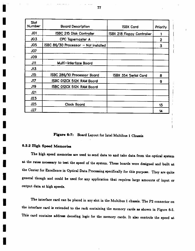
I
II
II
II
II
III
I
I
III
I
77
SlotNumber
J01
J03 CPC Topemaster A
J05
J07
Board Description
ISBC 215 Disk Controller
iSBC 86/30 Processor - Not installed
J09
Jll Multi-interface Board
J15
J15 ISBC 286/10 Processor Board
iSBC 012CX 512K RAM Board
ISBX Card
ISBX 218 _oppy Controller
iSBX 554 Serial Card
Priority
1
2
3
8
J17 9
J19 ISBC 012CX 512K RAM Board
J21
J23
J25 Clock Board 13
J27 14
Figure @-7: Board Layout for Intel Multibus 1 Chassis
a.8.2 High Speed Memories
The high speed memories are used to send data to and take data from the optical system
at the rates necessary to test the speed of the system. These boards were designed and built at
the Center for Excellence in Optical Data Processing specifically for this purpose. They are quite
general though and could be used for any application that requires large amounts of input or
output data at high speeds.
The interface card can be placed in any slot in the Multibus 1 chassis. The P2 connector on
the interface card is extended to the rack containing the memory cards as shown in Figure 6-5.
This card contains address decoding logic for the memory cards. It also controls the speed at

III
II
I
II
III
II
II
II
I
78
which the system runs by dividing down either an internal 20 MHz oscillator, or an external
oscillator, by two and then using a programmable counter to divide this clock by one to sixteen.
The divided clock is then sent to three circuits that individually delay the clock for data to be
sent to or from the PI' P2 and P3 sections by small intervals and supplies the memory boards
with these delayed clocks. This allows the user to produce slight time adjustments between the
data in both AO Cells and the detector plane. This is necessary since there is a delay associated
with the AO cells (5-800 ns) and since the physical distance between modulators and detectors is
large (5-10 ns for optical propagation of light).
This card is accessed through five 8 bit I/O ports. One port is used to set the clock speed
and to set and check the board status. The other three ports are used to delay the clocks with
the lower four bits being a fine adjustment of about 4 nanoseconds and the upper four bits being
a coarse adjustment approximately equal to the period of the master clock, usually about 50 ns
(20 MHz clock).
We presently have six memory cards configured as four output cards and two input cards
on the Intel system. There are also two output cards and one input card on the PM68K. Each
memory card contains eight data memory channels 4096 words long and 12 bits wide. There are
also two sequence control channels on each memory card that allow simple looping operations
and are also 4096 words long. The memory boards run at a 10 MHz rate per channel. The
memory cards are accessed in I/O space on the main system by setting an address counter port
and reading or writing a transfer port. Another I/O port allows the boards to be reset and
allows one to change certain status fields particular to each memory board. When a board
encounters a stop instruction in the sequence memory, it signals the interface board via a DONE
line.
79
6.4 Multi-Channel Encoded Processor Hardware
The analog hardware for this optical Matrix-Vector system is now discussed. This
hardware was built to provide the high data rates the system requires. The high-speed analog
hardware is shown in Figure 6-8. It consists of:
1. A clock board to provide all the components with the proper clock frequency at the
proper time.
2. Multiplexers (MUX) to provide the 40 MHz data rate needed from the 10 MHz
memory boards. (These boards were recently constructed and are presently beingtested)
3. Very fast D/A converters (4 bits _ 200 MHz, 3 bits used) to drive the AO cells. (One
per AO channel)
4. An RF driver card for each AO channel.
5. An oscillator shared by all drivers to provide input data to both AO cells at the
correct center frequency.
6. Optional secondary oscillators to allow for frequency-multiplexing of additional data
at other center frequencies.
7. A fa_eplate consisting of 10 (presently 3 exist) precisely aligned SELFOC lenses
feeding fiber optic cables to couple the light to the detectors.
8. A discrete detector array consisting of 10 amplified photodetectors and amplifiers to
control and adjust the gain and offset of the detector output. (One per detector)
9. Inverting buffers used to make the positive going output from the detector box
negative going to be compatible with the A/Ds used. (One per detector)
10. 100 MHz 6 bit A/D boards to digitize the photodetector outputs. (One per detector)
11. A precision reference supply for the A/D converters. (not shown)
12. A Shift and Add board used to emulate a high speed CCD type output detectordevice in hardware.
13. A demultiplexer to reduce the 40 MHz data rate from the shift/add board to the 10
MHz rate of the memory boards. (Not included at this time)
Many of these parts have capabilities that exceed what is needed for their respective
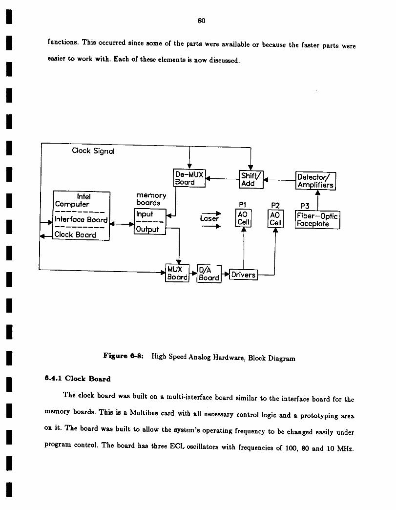
8O
functions. This occurred since some of the parts were available or because the faster parts were
easier to work with. Each of these elements is now discussed.
I
I
I
I
II
II
II
Clock Signal
Inlel
Computer
Interface Board
Clock Board
H
De-MUXL lShiff/LBoard r" JAdd F
I Detector/JAmplifi, ers ]
memory 1kboards P1 P2 P3
Input __._ "---_ _ F_CA,_1_1 IFiber-OpficLaser [Faceplote l
!Output _ l
_ Dr,versJ---
Figure 6-8: High Speed Analog Hardware, Block Diagram
6.4.1 Clock Board
The clock board was built on a multi-interface board similar to the interface board for the
memory boards. This is a Multibus card with all necessary control logic and a prototyping area
on it. The board was built to allow the system's operating frequency to be changed easily under
program control. The board has three ECL oscillators with frequencies of 100, 80 and 10 M_Iz.
I

81
The outputs of the oscillators are fed into a 4-1 multiplexer controlled by an I/O port on the
computer. This multiplexer selects which oscillator is to be used. The output of the multiplexer
is then fed into a ECL counter that provides -_-2, --}-4, -+-8, -+-16 outputs. The multiplexer
output is also fed into two other 4-1 multiplexers along with the -}-2, -}-4, -_8 otitputs of the
counter. One of these multiplexers is used to feed an ECL-TTL converter and send a clock signal
to the high-speed memory interface board. The other multiplexer sends a signal to two
programmable ECL delay lines, which are used to adjust the timing of the multiplexers,
shift/add and demultiplexer boards to be compatible with the memory boards and with the
optics. The outputs of the delay lines are buffered and sent to the ECL boards differentially to
minimize noise problems. Since we are presently not using the multiplexers, the shift/add board
obtains its clock signal from the input memory board via the cable it uses to send data to the
memory board.
6.4.2 Mux/DeMux Board
Since the system presently built does not require data rates higher than 10 MHz and since
fast ALU chips were not available when the system was constructed, the Mux/Demux system has
not yet been fabricated. If we build larger systems that use multi-channel AO cells in Pr data
must be fed to the optical system faster (and with more channels of data) in order to utilize the
information presently in the P2 AO cell.
The design recently constructed consists of TTL-ECL converters, ECL 4 to 1 multiplexers
and ECL differential drivers (OR-NOR gates). The board will derive its timing signals from the
clock board. To increase the speed we consider each 12 bit memory channels as four 3-bit words
of data and we use the multiplexers to switch between these words. This gives us a three bit
output at four times the input rate. The only anticipated problem is obtaining the correct timing
which should not be too difficult using the clock card.
82
6.4.3 ECL Shift/Add Board
In order to perform the convolution needed in the DMAC algorithm used, we use a time-
integrating architecture. Since a CCD type detector of the required capabilities is not available
at this time, we implemented the same function in digital hardware. This board performs that
function by taking the output from the A/Ds and adding that data to the data stored from the
previous add. This method also gives us certain advantages such as being able to monitor the
data at any point in the output system.
This board was built on a special ECL wire-wrap panel 26 designed for speeds up to 100
MHz. A two channel board was wire-wrapped locally to test the design and the ten channel
version was wire-wrapped by Augat using a special program that made sure twisted pairs were
used for wires longer then a critical length and that all lines were properly terminated. The
program also provides a large amount of information about wire lengths and other parameters
that are helpful in debugging the board. A photograph of the board is shown in Figure 6-9.
This board has nine adder-latch blocks and some discrete logic to control their operation.
It consists of ALU's and latches designed to emulate a CCD array, but at much higher speeds.
The latches are used to perform a shift of one location per clock cycle. The shift/add array can
perform three basic operations. These are:
1. To feed data from the A/Ds directly to the latches. (RESET)
2. To add the new input A/D data and the data in the prior latch.
3. To shift data from one latch to another through the ALUs.
The control section logic for the shift/add system is shown in Figure {}-10. It operates from two
,t-bit counters wired as a 5-bit counter. This gives a counter with a maximum output of 32 and
allows for a maximum of 32 cycles or operations (i.e. 32 TI). The number N of cycles (T2-----NT1)
is set by a 5-bit comparator fed with the counter data lines as one set of inputs and 5 position

OF BOOR QUAL{T3_
83
Figure 6-9: Picture of the ECL shift/add board
DIP switch data as the other inputs. When the comparator indicates that the outputs are equal,
a reset signal is sent to the counter to reset it to zero. This reset signal is different from the
RESET signal used as a control signal to the ALUs.
The ALUs have five inputs that control the function they are to perform. Since only three
functions are needed as enumerated above, the control logic is somewhat simplified. The control
lines on the ALUs are fed to inverters with enable inputs. When the enable line is low, all the
inverter outputs are forced low. This line is controlled by a 5-bit comparator, allowing the
RESET operationto occur on only one of the 32 possiblecycles.The inputsto the invertersare
eitherforced low or high, or are controlledby a set of multiplexers.The multiplexerinputs are
forced high or low depending on whether the current cycle is to be a shiftor an add/shift
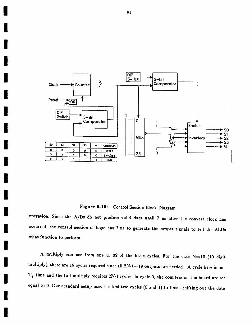
84
5//
_5-Bit 1
Comparator _--
so ! s_o i o
ol,o q ,
I
0 J o o _.S£T
1 I 0 o Shlft/Acld! 0 I I ! ._ft
MM
DIP .__._Swih:n i 5-bit_ =] Comparator
i
I--'_0
• MUX• i
I
L_.__ Enable
0
Inverters
= SO$I
, _ 52$3
=M
Figure 6-10: Control Section Block Diagram
operation. Since the A/Ds do not produce valid data until 7 ns after the convert clock has
occurred, the control section of logic has 7 ns to generate the proper signals to tell the ALUs
what function to perform.
A multiply can use from one to 32 of the basic cycles. For the case N-_-10 (10 digit
multiply), there are lg cycles required since all 2N-I_--lg outputs are needed. A cycle here is one
T 1 time and the full multiply requires 2N-I cycles. In cycle 0, the counters on the board are set
equal to 0. Our standard setup uses the first two cycles (0 and 1) to finish shifting out the data
i
85 -86
left in the latches from the previous multiply to the input memory board. This is required since a
sample at time 0 on the A/D appears on the A/D output pins two cycles later. On cycle 2, we
perform a RESET operation which loads the outputs of the A/Ds into the latches through the
ALUs. An add/shift operation is done for the next N-1 cycles. With 10 detectors this is 9
add/shift cycles. We then perform a shift for N-3 cycles to output the data remaining in the
latches. We use N-3 cycles since two shifts are performed in cycles 0 and 1. These N-1 shift
cycles could be avoided (or pipelined) by using a second set of latches. The second set of latches
are not included on the present board. For a two's complement system, this second set of
adder/latches would be useful. However, we plan to use negative base number representation
techniques that do not require this second set of latches. The ECL shift/add board outputs a 12
bit (with up to 10 bits significant) ECL signal at the fast clock (T1) frequency.
The clock circuits that control the adders have been tested at speeds up to 70 MHz.
Decoding delays in some of the logic, plus the time for an add (worst case approximately 15 ns)
place an upper limit of about 40 MHz on the complete circuit. We tested the circuit design at 10
MI-Iz using presently available 10K ECL adders (add time approximately 24 ns). We can
upgrade the device using fast ALUs that are now available. As noted earlier, the multiplexer is
not used or needed at present, although it is being worked on. The 10KH parts operate with half
the propagation delay of the regular 10K ECL parts with no increase in power requirements.
6.4.4 100 MHz fl-bit A/D Boards
These A/D chips exceed what is presently required by the rest of the system except for the
D/As. These parts were used because they were available. The excess capacity is useful since we
have more confidence that the A/Ds will work correctly at the data rate that they are being fed.
Alternatively, we could have purchased 40 MHz A/Ds that have a higher resolution (about 8
bits). This would allow us to use more channels or higher radix numbers.

87
Each A/D board has one TRW 1029J100 1Vfl-Iz6 bit flash A/D converter with an
impedance matching network as shown in Figure 6-11. The impedance matching network is used
to terminate the input with a 50 ohm load and to provide the A/D with a 18 ohm source as
specified on the TRW data sheet 27 . The board is designed to be inserted into a 24 pin, 0.6"
wide socket on the shift/add card which also supplies the necessary clock pulses, references and
power supply voltages. Each A/D board is designed with a large ground plane to help minimize
noise. All supply and reference voltages are decoupled on the board as close to the chip as
possible.
Figure 6-11: Photograph of one 6 Bit, 100 MHz A/D board
6.4.5 A/D Reference Supply
The reference voltages for the flash A/D converters are furnished from an external supply
board. The flash A/D converters require one volt across the resistor ladder with the Rb (Resistor
ladder bottom) voltage of-0.3 V and an Rt (Resistor ladder top) voltage of -1.3V 27. The board
uses an LM368-10 precision 10 volt reference. This supplies inputs to two LH0021CK 1-amp op
OF I_)OR QU_
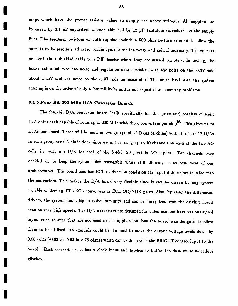
88
amps which have the proper resistor values to supply the above voltages. All supplies are
bypassed by 0.1 pF capacitors at each chip and by 12 #F tantalum capacitors on the supply
lines. The feedback resistors on both supplies include a 500 ohm 15-turn trimpot to allow the
outputs to be precisely adjusted within specs to set the range and gain if necessary.-The outputs
are sent via a shielded cable to a DIP header where they are sensed remotely. In testing, the
board exhibited excellent noise and regulation characteristics with the noise on the -0.3V side
about 1 mV and the noise on the -1.3V side unmeasurable. The noise level with the system
running is on the order of only a few millivolts and is not expected to cause any problems.
6.4.6 Four-Bit 200 MI-Iz D/A Converter Boards
The four-bit D/A converter board (built specifically for this processor) consists of eight
D/A chips each capable of running at 200 MHz with three converters per chip 28. This gives us 24
D/As per board. These will be used as two groups of 12 D/As (4 chips) with 10 of the 12 D/As
in each group used. This is done since we will be using up to 10 channels on each of the two AO
cells, i.e. with one D/A for each of the N+M-_-20 possible AO inputs. Ten channels were
decided on to keep the system size reasonable while still allowing us to test most of our
architectures. The board also has ECL receivers to condition the input data before it is fed into
the converters. This makes the D/A board very flexible since it can be driven by any system
capable of driving TTL-ECL converters or ECL OR/NOR gates. Also, by using the differential
drivers, the system has a higher noise immunity and can be many feet from the driving circuit
even at very high speeds. The D/A converters are designed for video use and have various signal
inputs such as sync that are not used in this application, but the board was designed to allow
them to be utilized. An example could be the need to move the output voltage levels down by
0.03 volts (-0.03 to -0.63 into 75 ohms) which can be done with the BRIGHT control input to the
board. Each converter also has a clock input and latches to buffer the data so as to reduce
glitches.
I
III
II
II
II
III
I
II
II
8O
If the multiplexer is put in use, we will only be using the top three bits of the 4-bit D/A
converter. This multiplexer is designed to use only three bits. This was done since we desire a 40
MHz rate in the multi-channel system, whereas if we used four bits the data rate would only be
30 MHz from the 12 bit, 10 MHz memories. We presently use all four bits on the initial test
system since there is no multiplexer. These D/As could also be used with different multiplexer
designs to provide 4 bits of data at 200 MHz if needed. Using four bits gives an output voltage
swing from 0.000 to -0.450 volts into 50 ohms. Since the D/A converters have internal 75 ohm
resistors, it was necessary to use external 150 ohm resistors to match the line impedance (50
ohms). Future versions of the D/A converter are planned that will allow for higher voltage and
current levels when driving a 50 ohm line. When these parts become available and if a greater
voltage swing is needed to drive the RF mixers, these units should be directly compatible with
the present PC board layout. Sample outputs from the 4-bit D/As are shown in Fig. 6-12.
0.4.7 RF Drivers and Oscillators
The RF driver boxes contain local oscillators, splitters, mixers, combiners and amplifiers.
The actual design of the box can be separated into two sections, the oscillator board and the
driver boards. The oscillator section provides the RF frequencies that are used to drive the RF
inputs on the mixers. The driver boards have the circuitry necessary to modulate the RF input,
perform frequency multiplexing and amplify the resultant signal to be able to drive an AO cell.
We have oscillators with frequencies of 300.000000 and 400.00000 MHz. We use two
frequencies since one of our 32 channel cell operates at 300 MHz and the other at 400 MHz. Each
oscillator is amplified and fed into a splitter network to provide multiple outputs with the same
frequency and phase. This part of the system uses SMA style cases and coaxial cable to
interconnect all the components.
The outputs of the oscillator section and the D/A section are used as the inputs to a Level
I

I
I
III
I
III
II
II
I
II
II
I
9O
Figure 6-12: Four bit D/A generating a random output

91
13 RF mixer. The Level 13 refers to the LO input specifying that it should be +13 dbm. Each
driver board has room for three mixers with two mixers presently installed. This was done to
allow us to handle complex data that needs two-channel frequency-multiplexing. The outputs
from the three mixers are fed to a three-input combiner. The output of the combiner is fed to an
impedance matching network since an CATV amplifier is used that needs a 75 ohm input and
the mixers are 50 ohm devices. The matching network is needed to extract the full performance
of the amplifiers and to reduce excessive power dissipation (heat). The amplifier output is then
fed through another matching network to match the 75 ohm output with the 50 ohm AO cell's
input impedance. The driver cards are built on a PC board using stripline techniques.
6.5 Detector Array and Fiber Optic Coupling
The optical system's outputs are piped by fibers which are then connected to the detector
system. The detector array consists of ten Merit 1900 hybrid photodetectors capable of 100 Mitz
operation, each with an integral pre_amplifier on the hybrid as shown in Figure 6-13. The pre-
amplifier (detector) output is then amplified by a high-power, wide-bandwidth amplifier capable
of driving a 50 ohm line. The detectors are all mounted on a single copper heat sink in order to
keep them all at approximately the same temperature. This is needed so that output variations
due to detector temperature are somewhat constant over all the detectors. The detectors are
very sensitive and exhibit a drift of about 10-20 mV/° C. Since the output is amplified with DC
coupled amplifiers, this drift is made worse. We counter this by leaving the detectors on at all
times and attempt to keep the room at a fairly constant temperature.
The amplifiers on the card are of a hybrid type made by Comlinear. They have
adjustments for gain, offset and crossover. The gain and offset are fairly standard adjustments
except that the gain is somewhat affected by the crossover adjustment. Since the Comlinear amp
has a temperature drift that effects the gain at low frequencies, a second op-amp is included on
92
I
II
II
II
II
III
I
the board to handle lower frequencies and it stabilizes the gain in this region. The crossover
adjustment is used to control the region where the second op-amp has an effect. The
recommended gain setting procedure is to feed the input of the circuit with a 70 kHz square
wave and adjust the crossover adjustment for best symmetry. Since we have a gain trimpot
installed that can vary the gain of the amplifier over a wide range, some resistors have to be
changed once an approximate gain setting is made to put the crossover control in the correct
operating region. The proper initial adjustment procedure for the detector amplifiers is to first
feed in a normal operating signal pattern and adjust the gain control for the desired output. A
good program to use for this is in the :prog:c/setone directory called CPP. It outputs a pattern
with a single pulse, three off-cycles, three on-cycles and then 6 off-cycles. This pattern repeats
every 13 cycles. We then run a program in the same directory called SEVENTY that feeds the
system with a 70 kHz square wave to adjust the crossover. If the trimpot does not have sufficient
travel, the operator must calculate a new resistor value based on the Comlinear data sheets. The
proper offset is about 0.43 volts to turn on the least significant bit of the A/D. Since we are
presently using the third bit, the easiest method to adjust the offset is to monitor the A/D
outputs on the logic analyzer, then run a program such as the CPP routine mentioned above and
adjust the offset until only the least significant bit used (bit three) is switching.
The detectors used are physically large, compared to a CCD or an integrated detector
array. In order to couple the output light to the detectors, we use a fiber-optic setup to pipe the
light to the detectors. This is achieved by a faceplate with SELFOC lenses and fibers placed in
the P3 output plane shown in Figure 6-14. The SELFOC lenses are the small rod elements at the
front of the metal holding block. These are attached to the block first. Then the fibers are
butted up against the SELFOCs, aligned with a laser and attached. The stack of metal plates on
the back of the assembly are used as strain reliefs. A SELFOC lens is a thin rod of a lens type
material that has been doped such that its refractive index varies radially. This makes the rod
93
act like a lens even though it has flat surfaces. These SELFOC lenses are coupled to fiber optic
cables that have a connector on the other end designed to plug directly into the detector case.
The SELFOC lenses used are 1 mm in diameter, 2.55 mm long and have a pitch of 0.25. The
coefficient of refractive index distribution is 0.{}158 mm "1 at 630 nm. The fibers used to connect
the SELFOCs to the detectors are a multimode type with a core size of 100 #m. The SELFOCs
are placed on 2 mm centers. The present version has some alignment problems (discussed under
system construction in sections 6.9 and 6.10). We have recently found new methods of fiber
coupling29, 30 and plan to use these in the ten channel system.
6.6 Software
This section describes the software written to operate the Matrix-Vector processor. This
software consists of an assortment of low level routines that handle loading of the high speed
memory boards, converting bases, decoding the detector outputs and various other functions. A
multiply routine is then written with the low-level software. The low level software is detailed
in Section 6.7. The top level of software consists of modified versions of LAE solutions written
to solve finite element or similar problems.
All software is presently written for a single input M-----1 channel system with N-_-3
channels at P2 and an LU solution of the LAE. We perform all multiplications with 21 bit input
accuracy. The software has most of the necessary controls to be able to operate larger optical
systems. It also has the capability to handle bipolar numbers and varying bit widths. Most of the
basic software is common to any LAE solution, iterative or direct.
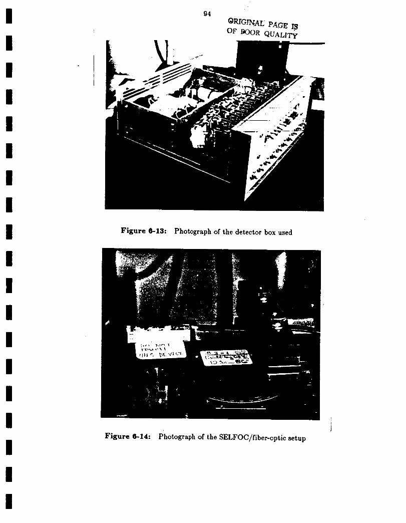
II
II
II
II
II
II
lI
II
II
I
94
OF I_OR QUALITy
Figure 6-13: Photograph of the detector box used
Figure 6-14: Photograph of the SELFOC/fiber-optic setup

II
II
II
II
II
II
II
II
II
95
6.7 Low Level Routines
These subroutines are designed to make it unnecessary for the user to be concerned with
hardware details.They take care of all the memory board functionsvery efficientlywith the
code written in C for compatibility. They also determine where data is to be placed on a
memory board and they perform base conversions.
a.7.1 Data Handling Conventions
The software must be able to handle bit lengths longer than the number of P2 channels
used and it also must be able to handle fractional numbers. The longer bit lengths require more
time, but show the flexibility of the system to be configured to run any number of bits
dynamically. We now show how this is done on our N_--_3 channel demonstration system.
Step 0 in Figure 6-15 shows the operations on a full system to perform a 9-bit multiply on
a system with N_-_-3 channels at P2" We feed the three least significant bits (LSBs) of the
multiplicand to P2 and run the 9 bits of the multiplier into P1 as shown in step 1 of Figure 6-15.
We then feed the next three bits of the multiplicand to P2 and repeat the 9 bits of the multiplier
at PI" This sequence is continued until the 9 bits of the multiplicand have been fed into P2" The
final output is assembled by shifting the second output product (from step 2) by three bits and
_lding it to first product (from step 1). The third and successive output products are shifted by
6,9,12 etc. bits and added to the previous total. The proper ordering, shifting and handling of
the data and these steps are performed in the multiply, memory load and unload routines. This
method thus allows us to perform a multiply of any length on an optical system of any length. It
is obviously preferable (from time considerations) to have N large, but with this method, we can
easily trade accuracy and hardware costs for speed (depending on the problem being performed).
The actual time for a multiply to be performed on the lab system is therefore,
I

96
Step 0101101101
001011100
101101101
101101101
101101101
101101101
102223323221100
(385)C 92)
Step 3 Step 2 Step 1
101101101 101101101 101101101
001 011 100
101101101 101101101
101101101
10110110100
101101101 >..... l 1112112111 >--I 10110110100
I I-> 1112112111
l.................... > 101101101
102223323221100 (33580)
Figure 6-15: 9 Bit Multiply on an 3 Bit Optical System
(B/N) x (N + B-- 1)xT 1 (6.1)
where the number of channels in P2' N, on the lab system is 3 and the bit length, B, is 21. The
previous chapters that define T 2 as being 2N-1 cycles (each T 1 long) consider the system to be
performing an N bit multiply on an N bit system. The T 2 for the product of each N bit word by
a B bit word is N+B-1 cycles (each T 1 long) in the lab system since that is the length of the
convolution being done.
In an LAE solution, the equation to be solved is,
(6.2)
In the finite element problem and many others we intend to solve, there are many purely
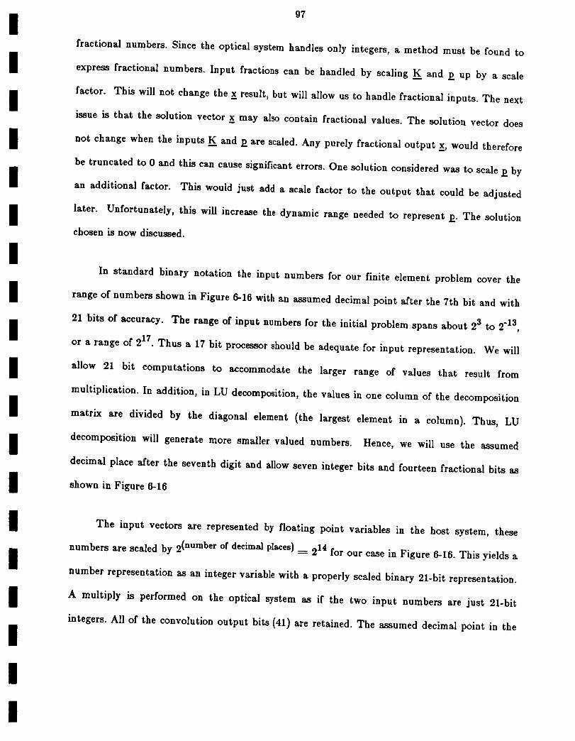
97
fractional numbers. Since the optical system handles only integers, a method must be found to
express fractionalnumbers. Input fractionscan be handled by scalingK_=and p up by a scale
factor. This willnot change the x result,but willallow us to handle fractionalinputs.The next
issueisthat the solutionvectorx may alsocontain fractionalvalues.The solutionvector does
not change when the inputsK. and p are scaled.Any purelyfractionaloutput x, would therefore
be truncated to 0 and thiscan cause significanterrors.One solutionconsideredwas to scalep by
an additionalfactor. This would just add a scalefactorto the output that could be adjusted
later. Unfortunately,thiswillincreasethe dynamic range needed to representp. The solution
chosen isnow discussed.
I
i
I
I
i
I
i
In standard binary notation the input numbers for our finite element problem cover the
range of numbers shown in Figure 6-16 with an assumed decimal point after the 7th bit and with
21 bits of accuracy. The range of input numbers for the initial problem spans about 23 to 2 "13 ,
or a range of 217. Thus a 17 bit processor should be adequate for input representation. We will
allow 21 bit computations to accommodate the larger range of values that result from
multiplication. In addition, in LU decomposition, the values in one column of the decomposition
matrix are divided by the diagonal element (the largest element in a column). Thus, LU
decomposition will generate more smaller valued numbers. Hence, we will use the assumed
decimal place after the seventh digit and allow seven integer bits and fourteen fractional bits as
shown in Figure 6-16
The input vectors are representedby floatingpoint variablesin the host system, these
numbers are scaledby 2(number ofdecimalplaces)____214 forour case in Figure 6-16.This yieldsa
number representationas an integervariablewith a properlyscaledbinary 21-bitrepresentation.
A multiply is performed on the opticalsystem as ifthe two input numbers are just 21-bit
integers.All of the convolutionoutput bits(41)are retained.The assumed decimal point in the

I
I
I
I
II
II
!
98
output is located at twice the number of bits that were to the right of the decimal point in the
original input data, i.e. at 2 x 14 _ 28 bits to the left of the least significant fractional bit as
shown in Figure 6-16. The integer part consists of the other 13 bits. We then truncate the output
to be the same number of bits (21) as our input with 7 bits to the left of the decimal point and
14 to the right. In doing this, we first discard the 14 least significant bits. We then check to see
if the integer portion is greater than 27 which would indicate an overflow. If an overflow
occurred, we set the value to the largest possible number in our notation. In the optical system,
we compute all 2N-1 output bits and then discard the low-order bits and perform this overflow
check. Since scaling is very problem dependent, it is performed in the high-level software such as
the LU decomposition routine.
In standard binary notatlon the Input numbersfor our FE problem range"
from 8.3770000 = 0001000.01100000100000
to 0.0002115 = 0000000.00000000000011
7 14
Output numbers will therefore have the form
l111111111111.dddddddddddddddddddddddddddd
13 28
Figure 6-18: Assumed Decimal Point Handling
6.7.2 Hardware Dependent Routines
These routines include the functions necessary to load the data and sequence memories,
start the processor running and the software to unload the memories. These routines depend on
what hardware is present and how many channels of the processor are being used. In order to
maintain processor speed, they are fairly specific to the processor set-up. They are also very easy
to modify though to use different architectures. The multiply code calls these subroutines in a
standard manner.

99
I
I
I
I
III
II
II
II
II
6.7.3 Scalar Multiply Routines
There are four versions of this routine that are obtained by linking with the appropriate
object code. Two of the routines perform the multiplications optically and the other two are
simulation routines. All four routines are called with the same parameters so the high-level
program does not need to be changed to switch between simulation and optical processing. All
input numbers are integer long variables (32 bits). One of the variable passed tells the processor
what
1.
bit length to use for the multiplies. The routines are different as follows,
FMULT - This routine uses high levelC code to perform the multiplicationsin
floatingpoint.This routinewas used to debug the high levelcode and to verifythe
resultsof the other multiplicationroutines.
. DMULT - This routine simulates the optical processor in detail. It calculates what
numbers would be read from the memory boards and calculates the output from this.
This was instrumental in eliminating some errors from C compiler problems. Since
the optical system is very reliable, this procedure can be used to simulate the optical
processor on any system.
. OMULT - This performs the multiplications on the optical processor. It calls all of
the memory load and unload routines and calculate various control parameters for
the system.
. UMULT - This performs identicalto OMULT except that it considers the input
numbers to be unsigned.This isused for most of the testand alignment software to
verifythe opticalsystem.
We are presently modifying the above routines to use multi-level data. Both simulators will
now run using 30 bit accuracy with radix 4 (2 bits) encoding. The hardware routines will require
some minor re-work in order to allow us to use the multi-level capability. This will increase our
accuracy by 9 bits, and speed up the multiply by a factor of two.
Work is also being done on methods to handle complex data either by doing four sets of
multiplies or by using the three-tuple method. We are also working on software to use the
negative base system to perform signed multiplies.
I

ii
I
II
I!
I!I
II
II
I
III
IO0
6.7.4 LU Decomposition Software
The LU decomposition software performs a direct solution to a LAE. The software also
takes into account the bandwidth of the matrix so as to reduce computation time. The user
inputs the data on the size of the matrix, the bandwidth and the number of input .vectors. The
program then reads the input matrix and vector data. It then generates an augmented matrix
and performs the LU decomposition and the backsubstitution to obtain the solution vectors. The
LU decomposition is performed on the optics since it is the major task and the backsubstitution
is performed digitally at this time.
6.7.5 Software list
Table 6-2 contains a list of all relevant software on the system.
• MEMORY LOAD
Loads the data into the electronic interface in the proper form.
• MEMORY UNLOAD
Retrieves the output data from the electronic interface.
• MULT0
Passes two real vectors to the optical processor, and returns the VIP.
• MULT1
Digital simulation of an optical MULT0.
• MULT2
Digital simulation of an optical floating-point multiply.
• CM MATH
Library of complex matrix operations.
• FM MATH
Library of floating-point matrix operations.
Table 6-2*- Table of System Software
i
101
6.8 Initial Laboratory System
We now describe the construction of the optical laboratory system. The first system,
described in Section 6.9, is a single bit system that uses a single channel AO cell in P1 and one
channel of a 10 channel AO cell in P2" This system was used to test our ability to align the
system timing, to drive the optical system and to verify our light budget. In Section 6.10 we
describe the three channel system that is used to test the electronic support system and to
demonstrate the use of the optical architectureto solve an LAE. This system uses a single
channel AO cellin P1 and threechannels ofa 10 channel AO cellin P2" This system usesbinary
T 2 -----.._ " mui_ipiJcs, willbe using thedata with T 1 _ 0.I ,as__nda o ._#s which allows21 bit I,.-_,-_We
method describedin Section 6.7.1(Figure6-15),where T 2 _ (N q-B - I)T1 _---(3 4-21 - 1)T1
23T 1.Hence N_3 channels at P2' B---_21bitsand T 2 _---23T 1 are used.
6.9 Single Bit Test System
i
i
i
I
I
III
6.9.1 Construction
This initial system was built to quantify how much light was available and to demonstrate
that we could perform a simple product of two binary inputs. When the initial design of the
system was completed, there was some concern as to how much light would be available on the
detectors after passing through the AO cells and the optics. This system was also used as the
test vehicle to align, calibrate and adjust the timing for the optical system. This was achieved
by running simple patterns into the AO cells and examining the output on an oscilloscope. The
system is diagrammed in Figure 6-17. The system was built using a single channel, longitudinal
TeO 2 AO cell in plane PI' one channel of a a ten channel, longitudinal TeO 2 AO cell in plane P2
and a single detector with amplifier.
The constructionof the system proceeded as follows.We firstoptimized the output of our
Spectra-Physics125 HeNe laser( k -----633 nm). The maximum output of the lasermeasured near
|

d
MemoryData
ITektronicslOscnlatorI _-_
II
il
[_E_ De.re.agnify I_ _ JOpt:cs iP1
HorizontalSlit
_lmaging_
Optics I "I IP2
J'crzv,r1_ox_
VerticalSlit
To InputMemory
Detector
P3
iI
IiI
Figure @-IY: Single @hannel Test System
its head was 61 mW. We found that the output power level of the laser would desrade by as
much as 50 percent over z week without periodic adjustments. This is due to the extreme 20" F
temperature variations in our labs. Thk is presently being corrected. A more typical variation is
5-10% over z day. This is not significant when running a problem since the laser output is quite
stable during the short time it takes to execute a problem. Calibration can be performed to
adjust for temperature variations if needed. Our new AC-coupled system should minimize this
problem.
! The next step was to demagnify the beam to increase the rise time of the output signal
II
I
from the AO cell in PI" The demagnification optics used consisted of a I00 mm lens with'a 150
pm pinhole at its focal point and an 18X microscope objective (fL --" 10 ram) to re-collimate the
beam. This reduces the beam width by a factor of I0 from 2.0 mm to 200 pro. A narrow optical
beam is necessary since the light beam leaving PI is the convolution, of the input signal with the
I
I

II
III
I
III
II
II
II
II
I
103
input laserbeam. The risetime of the output lightisthus dependent on the duration of the T 1
signaland the laserbeam width. Since the data travelsin the cellat 4.26 mm/ps, a T I data
packet covers a 200 pm distance in approximately 50 ns. Since T 1 _---100 ns, the output light
from P1 is150 ns in duration (theconvolutionof T1_100 ns and the 200 #m laserbeam width
which corresponds to a 50 ns width in terms of AO cellacousticvelocity)with a risetime of 50
ns, a flatoutput for 50 ns and a falltime of 50 ns. Demagnification increasesthe divergenceof
the output beam. Thus, to keep the sizeof the beam as small as possible,the AO cellin P1 is
placed as closeas possibleto the second fL-_--10mmdemagnification lens.This isdone because
increaseddivergence willreduce the efficiencyof an AO cell,which only givesa largediffraction
efficiencyfor lightwithin a certainrange ofthe Bragg angle.
When the opticalbeam leavesthe AO cellat P1 (AO1) it divergesboth horizontallyand
vertically.The opticalsystem between P1 and P2 consistsof three cylindricallenseswhich
images a magnified version of AOI onto AO2 horizontallyand thus the beam divergence
horizontallyisnot a major concern In the verticaldirectionthe diverging beam from AO1 is
focused onto AO2 by a third cylindricallens.This yieldsa verticallydivergingbeam leaving
AO2 with a horizontalwidth at P2 set by the width of the acousticchannel in AO2. This must
now be focussed onto the detector system at P3" In the firstsetup, (thissection),this was
achieved with a 30 mm sphericallens.In the second setup,(Section6.10)a fiberoptic detector
faceplatewas placed 10 cm from AO2 and the SELFOC on the detectorfaceplateserved to focus
the lightintothe fiberopticsused to coupleto the detectors.
The P1 AO cell is then placed in the beam and is positioned for maximum - 1 order
diffractionefficiency.The AO cellused has a centerfrequency of 200 N£[-Izand a bandwidth of
about 60 MHz. This ismore than adequate for thissystem which willonly be run at a maximum
of 10 MHz. The diffractionefficiencyof thisAO cellat the power level used is about five
i
I
i
I
II
I
I!
l
II
!1II
104
percent. Thus, much of the optical beam power is lost, but sufficient light exists to be quite
usable.
The drive circuitfor the P1 cellconsistedof a Local Oscillator(LO), a mixer and an RF
amplifier.A Tektronix model SG 503 Leveled Sine Wave Generator with a 10 db attenuatoron
the output and adjusted for a +7 dbm signalwas fed to the LO port of a Mini-CircuitsZFM-1W
mixer. The IF port on the mixer was fed with the output of the 4-bitD/A circuitdescribedin
Section 6.4.6.The mixer output was then fed through a 10 db attenuator to a Mini-Circuits
ZHL-1-2W RF amplifierwhich provided an output of about 50 mw RF to the AO cell.
The next step isto block the DC term leavingthe AO celland expand the -I order light
horizontallyso that itilluminatesallchannelsof the second AO cell.The input lightdistribution
isuniform within 5_ over threechannelsofAO2. This isachieved with a 12.7mm and 200 mm
horizontalcylindricallensmagnificationsystem. We then compress the beam verticallyto about
400 pm at AO2. This was achieved with a 300 mm cylindricallensand was necessarysincethe
beam divergesverticallyas itleavesPI" This isalsonecessarysincethe P2 AO cellhas a very
narrow verticalopening and the crystalissetback in itscase.The compression alsoprovidesus
with a smaller beam exitingthe cellthat is easierto image onto the output detector thus
increasingthe output lightdetected.
We then place the P2 AO cell in the system and adjust it for the correct Bragg angle by
checking for maximum output. This cell has a bandwidth of only 10 MHz, so it is just able to
handle the input signals we intend to use. In this system, the P2 input data rate used ranges
from about 0.4 to 10MHz depending on whether a problem or a test pattern is being run. The
main reason this cell was used rather than one of our 32 channel cells is that it has a much
higher diffraction efficiency of about 95 percent compared to 12 percent (for the 32 channel cell)
and in initial experiments we wanted as much light as possible. With the 100 ns pulse for AO2

105
usedwith test patterns,the vertical width of a data packet in AO2 is 200 pm or half the focused
optical beam size. When the finite element problem was run the pulses for AO2 were 2.3 ps long
to insure that P2 data is present for the duration of the 21 T 1 data packets in AO1. Thus the
amount of light leaving P2 varies depending on how the data is being fed to AO2. This is not of
concern since when running a given problem, we use one T 2 exclusively.
I
I
I
i
I
I
Ii
I
The P2 cell is driven by a driver box similar to the driver circuit we constructed for the PI
cell. It consists of a LO that drives 10 mixer-amplifier units. It has a slight offset so that a zero
output is obtained with a slightly non-zero input since it was designed to be driven with TTL
level signals. Since our D/A converters are not offset (i.e. they output zero volts for a zero
input), the amount of input offset on the drivers reduces the useable output RF range and hence
the number of levels we can represent. For the binary encoded system with one P1 channel
M_I, only two output levels are needed at each T 1 and the light level is sufficient for this.
We used a custom designed slit to extract only the +1 order beam from the P2 cell. Next
the beam is focused onto a Merit 1900 detector by a 30 mm spherical lens. This is a very
sensitive alignment since the light must not touch the barrel of the detector assembly. The
problem is that if the light reflects off the inside of the barrel, any vibration of the barrel
(including air currents) causes significant changes in the output. In this setup, we found that the
vibrations present can easily cause the A/D to sample an invalid number. We did not cut off the
barrel on the detectors since the barrel is needed to couple the optical fibers to the detector in
the detector system used with the three channel system (Section 6.10).
The output of the detector-amplifier is fed into an inverting buffer. A second amplifier was
necessary since the amplifier used with the detector could not be configured to invert, amplify
and bias the detector at the same time. The inverting buffer was made from a Comlinear
CLC-103 amplifier using a Comlinear circuit board. It has the added advantage of having a
|

106 ORIGI_ PA[GE /_
OF _,OR Ou_
precisionoffsetadjustment. The output from the detector system isfed to the I00 MHz A/D
converters,through the shift/add hardware and is collectedby the input memory boards. This
allowsus to verifythatwe can properlycollectthe data from the opticalsystem.
The next step isto set up the interfaceboard for proper system timing. This isdone by
running a program in the setone directorycalledPP that outputs 100 ns pulsesspaced 40 ks
apart to both AO cellsas shown inFigure 6-18.The detectoroutput ismonitored on a scope and
the timing delays are adjusted for a maximum output. The delaysin the AO1 and AO2 signals
_ J:.____ IL_° Ll _ ° •
are _uju_d ux keys on _.e _crrmnal as specifiedin the program. The sample clock forthe A/Ds
isthen connected to the scope along with the output of the detectorsand itsdelay isadjustedso
that the A/Ds are sampled at the proper time.These delays are then recorded and used forthe
variousmultiply routines.
Figure 6-18: Detector output from the timing setup program

I
I
I
II
I
III
II
II
II
II|
107
6.9.2 Results
We fed the system with various patterns and examined the output on an oscilloscope. A
typical test is as shown in Figure 6-19. The bottom trace is the digital input to AO2, the middle
trace is a ramp input to AO1 and the top trace is the detector output. The two-input traces
represent larger values as a more negative voltage (ground is the highest level on both input
traces). The output trace is positive going. To time align these figures the AO2 data should be
shifted to the right by two time slots (due to the delay in the AO2 cell). The three output peaks
represent the proper multiplication of the third, fifth, ninth and tenth levels on the AO1 ramp
by the AO2 unit pulses as shown in Figure 6-19. The detector outputs were then fed to the A/Ds
to verify that the A/Ds would sample the signal correctly.
This test demonstrates the timing alignment of the system, the ability of the electronic
support system to generate multi-level input data and the ability of the P3 electronics to process
multi-level output detector data. Our finite element case study will employ binary encoding and
thus does not require multi-level inputs or outputs. In these multi-level tests, detector noise and
drift were observed. The noise level of the detectors was adequate, being below one LSB of the
A/Ds (12 mV). However, since the detector output tended to drift with even the slight
temperature changes caused by the heating of the detector, we found it necessary to constantly
re-a_ljust the detectors offset so that the A/D outputs was a one when required. These and
similar steps were logical first steps that provided quantitative data on light budgets and tests of
all system parts. These system tests proved that the optical and electronic support system was
realistic.

108
_AI: PAng _.OF t_)OR QUAbrry
Figure 6-19: Test outputs from the single channel test system
6.10 Three Channel System
This system was built to thoroughly test and exercise the entire optical and electronic
support systems. We decided on three channels at P2 (N_-_3) since this would allow all essential
hardware to be tested and it was our first attempt at a fiber-optic faceplate. We use the same
cells as in the previous system with three channels of the cell in P2 now used.
6.10.1 Construction
This system is the same as the system in Section 6.g with the following exceptions:
1. The demagnification optics illuminating PI were redesigned to reduce its sensitivity
to mechanical vibration.
2. Three channels of P2 were used.
3. A SELFOC lens and fiber optic system was used to pipe the light from the P3 plane
to the detector box.
4. A detector box consisting of ten Merit 1900 detectors and amplifiers was employedwith three channels used.

II
I
II
II
I
log
5. The A/D converters were switched to use the third bit of the 6-bit A/Ds to
determine ifthe output was 0 or 1.This correspondsto 000100 or a 4 and thus 4(12)
---_50 mv of noise and drift.This was adequate for real-timeoperation with no
adjustments fordrift.
6.The functionsof the output shift/addarray were used.
These changes are now detailed.
The change in the demagnification optics was made after a thorough checkout of the
system to determine the components most sensitive to vibration. This was necessary since even
minor vibrations caused problems with the A/D output in the original system (Section 6.9). By
selective testing, the demagnification setup illuminating P1 was determined to be the prime
problem and the lasermount as a secondary problem source.The demagnificationopticswere
alteredby removing the pinholeand replacingthe pinhole-objectiveassembly with a lensof the
same effectivefocal length (10 ram) as the objective.This new lens system was sturdierand
much lessprone to vibration.Omitting the pinhole did not cause problems in the laserbeam
uniformity.The lasermounts were alsotightenedto minimize vibrationsfrom that part of the
system.
We then connected 3 channels of data to the second AO cell.Crosstalkwas visiblebetween
channels,but itwas down 20 db and did not cause a problem with our present use of binary
numbers. This willbecome more significantwhen multi-levelencoding isattempted.
The SELFOC assembly to coupleP3 tothe detectorconstructedconsistedof a metal block
holding SELFOC lensescoupled to fiberoptics.The major issuesto be addressed included
creating a useable fiber alignment jig and a suitableadhesive to hold everything in perfect
alignment when cured. Regular epoxies tend to shrink while curing causing a lossof proper
alignment.The four methods we consideredwere:
1.a UV epoxy

I
I
I
I
I
I
I
I
110
2. a super glue adhesive
3. to plate and solder the SELFOCs and fiber in place
4. an RTV type adhesive
A UV epoxy cures when exposed to UV light. Problems exist with the UV epoxy method since
the epoxy only cures skin deep and can thus be very fragile. We also did not have the capability
to plate the fibers and SELFOCs so we tried the super glue method. We found that this type of
adhesive also shrinks somewhat while curing and decided against its future use. We then used an
RTV type adhesive and had reasonable results with two of the three channels and the third
channel was only slightly out of alignment. It was physically moved into alignment while setting
up the system. This is possible since RTV is not a very strong adhesive. The specifications of the
SELFOCs and fibers used are given in Section 6.5.
This method proved satisfactory for the demonstrations needed to run the finite element
problems. We later ran into misalignment problems caused by an ageing effect with the RTV.
We then used a different construction method using the UV and regular epoxy that has proven
to be much more stable in the long term. We first used the UV epoxy to precisely align the
SELFOCs and fix them in place. We then aligned and attached the fibers with small amounts of
UV epoxy and, once set, used a regular epoxy for added strength. The assembly has remained in
perfect alignment for over 9 months at present.
The other end of the fibers was fed to the detector box consisting of ten Merit 1900
detectors, ten amplifiers and a precision reference used to bias the output to a suitable range.
The reference used was an LM368H-10 reference connected to an LH0021CK op-amp used as an
inverting buffer with a slight voltage adjustment. The output voltage was -9.00 volts. This was
fed to the bias circuit on the input of the detector amplifier. The detector box also has its own
power supply to reduce the number of wires and boxes used in the original detector system in
Section 6.9.
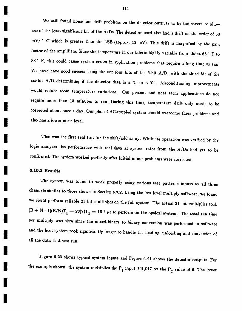
I
I
I
I
I
II
i
III
We stillfound noise and driftproblems on the detectoroutputs to be too severeto allow
use of the leastsignificantbitof the A/Ds. The detectorsused alsohad a drifton the orderof 50
mV/° C which is greaterthan the LSB (approx. 12 mV). This driftismagnified by the gain
factorof the amplifiers.Since the temperaturein our labsishighlyvariablefrom about 68 ° F to
88 ° F, thiscould cause system errorsin applicationproblems that requirea long time to run.
We have have good successusing the top four bitsof the 6-bitA/D, with the third bitof the
six-bitA/D determining ifthe detector data is a '1'or a '0'. Airconditioningimprovements
would reduce room temperature variations. Our present and near term applicationsdo not
require more than 15 minutes to run. During this time, temperature driftonly needs to be
correctedabout once a day. Our planed AC-coupled system should overcome these problems and
alsohas a lower noise level.
This was the first real test for the shift/add array. While its operation was verified by the
logic analyzer, its performance with real data at system rates from the A/Ds had yet to be
confirmed. The system worked perfectly after initial minor problems were corrected.
6.10.2 Remult8
The system was found to work properly using various test patterns inputs to allthree
channels similarto those shown in Section6.!}.2.Using the low levelmultiply software,we found
we could perform reliable21 bit multiplieson the fullsystem. The actual21 bit multipliestook
(B -k N - 1)(B/N)T 1 _ 23(7)T1 _ 16.1ps to perform on the opticalsystem. The totalrun time
per multiply was slow since the mixed-binary to binary conversion was performed in software
and the host system took significantlylongerto handle the loading,unloading and conversionof
allthe data that was run.
Figure 6-20 shows typicalsystem inputsand Figure 6-21 shows the detectoroutputs. For
the example shown, the system multipliesthe P1 input 161,017 by the P2 value of 6. The lower
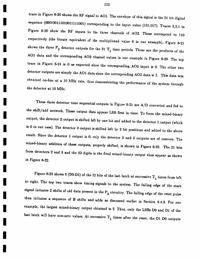
112
tracein Figure 6-20 shows the RF signalto AO1. The envelope of thissignalisthe 21 bitdigital
sequence (000100111010011111001) correspondingto the input value (161,017).Traces 3,2,1in
Figure 6-20 show the RF inputs to the three channels of AO2. These correspond to 110
respectively(the binary equivalentof the multiplicand value 6 in our example)..Figure 6-21
shows the three P3 detectoroutputs for the 21 T 1 time periods.These are the products of the
AO1 data and the corresponding AO2 channel values in our example in Figure 6-20.The top
trace in Figure 6-21 is 0 as expected sincethe corresponding AO2 input is0. The other two
detectoroutputs are simply the AOI data sincethe correspondingAO2 data is1. This data was
obtained on-lineat a I0 _u. rate,"_---........ .,..,.,.,., _,uu_ demonstrating the performance of the system through
the detector at 10 MHz.
I
i
I
I
III
I
I
These three detector time sequential outputs in Figure 6-21 are A/D converted and fed to
the shift/add network. These output data appear LSB first in time. To form the mixed-binary
output, the detector 2 output is shifted left by one bit and added to the detector 1 output (which
is 0 in our case). The detector 3 output is shifted left by 2 bit positions and added to the above
result. Since the detector 1 output is 0, only the detector 2 and 3 outputs are of concern. The
mixed-binary addition of these outputs,properlyshifted,isshown in Figure 6-22. The 21 bits
from detectors2 and 3 and the 23 digitsinthe finalmixed-binary output thus appear as shown
inFigure 6-22.
Figure 6-23 shows 6 (D0-D5) of the 12 bitsof the lastlatchat successiveT 1 times from left
to right.The top two tracesshow timing signalsto the system. The fallingedge of the start
signalinitiates2 shiftsof old data presentinthe P3 circuitry.The fallingedge of the resetpulse
then initiatesa sequence of B shiftsand adds as discussedearlierin Section 6.4.3.For our
example, the largestmixed-binary output obtained is2. Thus, only the LSBs DO and D1 of the
lastlatch willhave non-zero values.At successiveT 1 times afterthe reset,the D1 DO outputs
II
II
II
II
III
II
I
III
I
I
113
__ PA_E I_..
OF _iOOR QUAbI'rY
Figure 6-20: Example RF inputs to the AO cells
Figure 6-21: Example detector outputs

I
I
iI
Ii
II
114
000100111010011111001
110
000000000000000000000
000100111010011111001
000100111010011111001
00011012211101222210110
00011101011110111010110
A01 input
A02 inputs
Detector 1 output
Detector 2 output
Detector 3 output
Shlft/Add output
Flnal binary output
Figure 6-22: Action performed by the shift/add on the example problem
(left to right in Figure 6-23) are : 00,01,01,01,00,01,10,etc. These correspond to the mixed-binary
output: 0,1,1,0,1,2,etc. These correspond to the 6 least significant, digits in the mixed-binary
output in our example. The remaining outputs in Figure 6-23 correspond to the remaining digits
in the result. The mixed-binary output ends after 23 time slots at which point the reset pulse
reappears in Figure 6-23.
Figure 6-24 shows the converted binary representation of this mixed-binary output, this is
obtained in software on our system. The standard binary output for our example is :
011101011110111010110 as shown in Figure 6-24.
6.11 Summary
In this chapter we described and demonstrated an optical matrix-vector computer
architecture and a very flexible electronic support system. The system built can perform 21-bit
multiplies in 16.1 ps and can he expanded to perform 30-bit multiplies in under 0.5 /_s. The
system can also be expanded to compute a 10 element VIP in 0.5 ps (10 multiplications and
additions) or one multiplication/addition every 50 ns.
The electronicsupport hardware consistedof a host computer, a high speed memory
subsystem, A/D and D/A conversion hardware and custom shift/add circuitry.The host
computer isa Intel286/380 system that was customized for thissystem by adding a high speed

I
Il
Il
ll
ll
Ill
l
Ill
l
lI
Figure 6-23:
Figure 6-24:
115
ORrcrNArs PmcE ._OF 'l_O0_ QUALITY:.
Example mixed binary outputs
Example system final output
116
math co-processor,extra I/O ports for communication with the CEODPs VAX 11/750, a 1/2"
tape driveand specialsoftware to run the opticalsystem software.The software writtenincluded
routines for diagnostics,calibrationand operation of the digitaland optical system. This
includesmultiply routinesthat allow system usersto interfaceeasilyto the opticalprocessorand
an LAE solutionby the LU decomposition method. The four high-speedmemory boards feeding
the system are capable of supplying 32 12-bitchannels at a 10 MHz rate with each channel
holding 4096 words of information.The two input memory boards have the capabilityof
accepting 16 channels by 12-bitsof data at similar rates. We have demonstrated working
hardware that includes4-bit200 MHz D/As and @bit I00 MHz A/Ds. We alsobuiltand tested
an ECL shift/addoutput array that emulates a CCD detectorat 6-bitsand 10 MHz speeds per
channel (i.e.a 9-bit10 MHz CCD array)The shift/addcard was designed to work at 40 MHz.
Since thiswas the firstattempt at much of thishardware, ithas resultedin working designsfor
use with largersystems with fasterelectronicsupport.
We fabricated and tested the electronicsupport and optical processor and obtained
quantitativedata for lightbudgets and noiselevels.We demonstrated that we could operate our
testsystem at a 10 MHz clock rate with no problems and can foreseeno problems with clock
ratesof up to 40 MI-Iz,which isthe highestspeed we presentlyanticipateusing.
The major purpose of this part of the project was to assemble the electronic support
system to allow us to obtain quantitative data on an initial optical lab matrix-vector test bed
and to define and qualify directions for future research on such systems. The highlights of our
work are now Itemized:
• The electronic system requirements for an optical matrix-vector processor with M
processor channels with N digits accuracy and multi-level encoding was quantified.
(Section 6.2)
• A new electronic support system with an Intel host processor and superior hardware
and software support was designed and fabricated. (Section 6.3)
117
• The hardware system provides much higher data rates and accuracy than any other
previous optical matrix-vector system.
• A new technique to realize any desired accuracy using any number of digits on the
processor was devised and demonstrated. (Section 6.7.1)
• The software routines for the system are much more user friendly than with any
other optical matrix-vector system. (Section 6.6)
• The firstexperimental demonstration of a direct LAE solution on an optical
processorwas provided.(Section6.10)
• The ability of the electronicsupport system to handle multi-leveldata was
demonstrated. (Section6.9.2)
• The opticaland electronicsupport was shown to produce practical21-bitaccuracy
multiplicationswith an errorratebelow 10-7.
• We obtained quantitativedata on the lightbudget, noise and driftthat willprove
valuable in buildingfasterversionsofthisprocessor.

118
7. LABORATORY OLAP PERFORMANCE AND
PLANS
The prototype laboratory OLAP was described earlier in the Spring 1986 report to
NASA 31. Some qualitative and quantitative results of initiM performance tests for single
multiplies and multiplication tables were reported earlier. Since that time, the laboratory OLAP
system was used to run a static finite element plate bending case study. The case study was
detailed elsewhere. The results of this 0LAP demonstration are given in Chapter 5 of this
report. In this present chapter, we discuss the current OLAP performance limitations, and our
plans to decrease or eliminate them with a new AC-coupled operating mode.
I
I
I
I
I
I
I
7.1 Laboratory OLAP Characterization
The laboratory OLAP system was extensively described in Chapter 8 of our Spring report
to NASA, and in Chapters 5 and 6 of this report. Only a brief description of the system is given
here for reference purposes.
7.1.1 Laboratory OLAP Symtem Review
A basic schematic of the laboratory optical system used is shown in Figure 7-1. The blocks
at PI' P2' and P3 are tilted for illustrative purposes only; the actual component orientations are
better illustrated in other figures. The laser beam is first compressed (demagnified) by a
combination of lenses in order to properly illuminate the AO cell at PI" The outputs of the PI
AO cell 1 are the zero-order and the first-order modulated beams. The zero-order beam is
blocked by a spatial filter, and another combination of lenses shapes the first-order beam such
that it properly illuminates the AO cell 2 at P2" The zero-order output of the P2 AO cell is
blocked by a spatial filter, and the first-order is imaged onto a P3 fiber-optic detector faceplate.
There are M channels at P1 and N channels at P2" The N bits of the M multipliers are fed
bit serially into the PI channels, and the N bits of the multiplicands are fed in word parallel
!

m llg
i form to the P2 channels. The convolutions of the multiplier and multiplicand bit streams aresummed onto the detector plane and appear in mixed radix form. The proper shift and adds
take place in ECL hardware to form the desired products.
I In the current laboratory OLAP, M-_-I and N_3. By using partial product partitioning of
the digital multiplication by analog convolution algorithm, we perform 21-bit multiplies. By
I using seven partitions and with N_3, we obtain a 21-bit processor.
I A A
I JLASER J_J OPTICS q OPTICS , OPTICS.
I y P P P2 3X I
I zFigure 7-1:
I
I
I
Laboratory Optical System Schematic
A block diagram of the laboratory system is shown in Figure 7-2. This diagram
emphasizes and illustrates the role of the electronic support hardware components. The support
hardware can be divided into four system components: the computer input and output high-
speed memories, the digital-to-analog converters (D/As) and RF driver/modulators for the AO
I
II
cells, the detectors/amplifiers and analog-to-digital converters (A/Ds), and the emitter-coupled
logic (ECL) shift and add detector hardware.
The high-speed memories are run at 10 MHz. The OLAP is tested in a burst processing
mode, where the output memories are loaded with the required data and dumped to the OLAP
I
I
at 10 MHz. One 12-bit output memory channel from the host computer is used to feed each of
the PI and P2 input AO channels. The D/As are four-bit converters which feed the required
I

120
levels to the RF driver/modulators for the PI and P2 AO cells at 10 MHz. At P3' a fiber-optic
faceplate collects the output light from P2 and routes it the detector/amplifier box. The
detected optical signals are amplified to the proper levels and then sent to six-bit A/Ds at 10
MHz on each output detector. The digital outputs are then processed by the ECL shift and add
hardware system. The input memories collect data from the ECL shift and add hardware at 10
MHz.
I HOST I--.J OUTPUTCOMPUTERI "1MEMORYID/A'SRFDRIVER/MODULATORSI
INPUTMEMORY I
Figure 7-2:
SYSTEM
(AO CELLS l& 2)
IDETECTORSAMPLIFIERS
A/D'S
SHIFT & ADD
Laboratory System Block Diagram
121
7.1.2 System Performance Limitations
Chapter 5 of this report describes how the laboratory OLAP performed very well when
running the static finite element plate bending case study. The processor ran with M_I, N---_3,
and B-_-2, ie. binary encoding. Earlier, 25 we discussed the digital error source simulation of the
OLAP for this same case study. Our laboratory results agree with the digital simulation results
by showing that the optical error sources are at a low enough level to allow error-free processing
with binary encoding. The specific error source levels were documented previously 31. No
statistical error rate was rigorously determined, but from the laboratory operation, it can be
,,o,,..._;"'_'"a.,.,,_at 1iv,,_l than 1 bit error in every _u bit multiplications. This estimate was obtained
by continuously running batch jobs on the system which performed all sizes of 21-bit multiplies
on the optical processor.
Although the laboratory OLAP works quite well in its present configuration, some
limitations do exist. These limitations were determined in the initial tests of the laboratory
OLAP setup, and were noted earlier 31. No new significant limitations were discovered when the
laboratory OLAP was tested for the initial case study. The two major limitations are light level
and detector drift. Both of these factors must be improved if we are to expand the laboratory
OLAP (in terms of the number of channels M and N, or in terms of the base B that we use).
The light levels at P3 of the OLAP are sufficient for operation with N-----3 and M_---1, but
an increase in N primarily (and M to a lesser extent), would decrease the light available at P3"
If the number of channels N were doubled, the light levels at P3 would be reduced at least by a
factor of 2. The decrease in light level is not as severe if M is increased, and mainly depends on
what type of modulator is used at PI" If we want to increase the base B used, more dynamic
range at the detectors, and thus a larger light level is required. Our detector/amplifier output
(for a binary 1) is currently about 50 mV, the detector/amplifier noise is approximately 10 mV

,122
peak to peak, and the A/D step size is 12.5 inV.
needed if B is to be increased.
Thus itisobvious that more output range is
Currently, the light incident on a singlechannel of the P3 fiber optic faceplateis
approximately 70 jaWatts, representinga binary 1. With a 3 dB lossthrough the opticalfiber
coupling,approximately 35 pWatts are incidenton the solidstatedetectors. The lightentering
the opticalsystem at P1 isabout 20 mWatts. Thus, the lightlossthru the system for M_I and
N_3 is approximately 30 dB. The shot noisefloorof the detectorsisseveralpWatts, thus the
P3 light levelscannot be lowered significantly.To remain at similar P3 light levelswhile
increasingN or M, the amount of lightintoP1 needs to be increased. To increaseB, we need
more lightat P3 to yieldmore dynamic range,thus we alsoneed to increasethe amount of light
into PI" This could be accomplished by usinga more powerful laser,or tuning up the one we
have (itiscapable of 50 mWatt operation).However, a more light-efficientscheme isto use a
high-power (20 to 30 mWatts) laserdiode at each P1 channel. Thus, as M is increased,we
increasethe amount of opticalpower input to the system. More important, we do not use an
acoustoopticmodulator at PI' which currentlyonly has a diffractionefficiencyof only about 5%.
The second important OLAP limitation is detector drift. The drift is due to thermal
effects and has two sources. The first, and probably the most important, is the ambient
temperature instability in our laboratory. The second source is the heating (or relative cooling)
of the detectors when they encounter a number of consecutive binary l's (O's) during processing.
The detector drift is often significant, as the detectors are specified to drift 10 mV/degree C,
which is about 20_ of our full scale output. The laboratory temperature instability is
correctable, and University plans call for correction of the problem, but it is not clear how soon
the problem will be corrected. The second thermal effect source is not as easy to eliminate. The
temperature of the detectors will always vary with the DC level of the incident light, which is

123
solelydependenton the numbersbeingprocessed.One solution that would eliminate the drift
problem from both sources is to AC couple the entire system. This approach will be detailed in
the next section.
At this point, another critical aspect of the laboratory OLAP merits attention, and that is
timing. As N and M increase, the system timing becomes much more difficult. This involves
ensuring that the data at P1 and P2 are in the right place at the right time, and that the A/D
samples and processes the detector/amplifier outputs at precisely the correct time. As the
number _r ch__nne!sM _A N _ the o,._o_ " .... a....... f r.ooa_,_ are introduced
which must be properly synchronized. Thus, as we increase M and N, we expect considerably
more precision to be required in system timing.
7.2 AC-Coupled OLAP
The previous section discussed the laboratory OLAP system problems that limit the
increase in the number of PI channels M, the number of P2 channels N, the speed, and the
encoding radix B. We have concluded that increases in M,N, and B will need to be accompanied
by an increase in the light level through the processor, and the elimination of detector drift. We
plan to increase the light level by using laser diodes for the P1 point modulators, as discussed
above. The problem of the detector drift remains, and the proposed solution is to AC couple the
system. This will negate the detector drift effects, which are essentially time-varying DC
components. The AC coupling is also necessary to properly operate the laser diodes without
substantial drift in their optical power output.

124
7.2.1 SaC Coupling Basics
To AC couple the optical system, the input light (from the laser diodes) will be AC
modulated. In the present system, the P1 point modulator (acoustooptic cell) passes light to
represent a binary 1, and does not pass the laser light to represent a binary 0. These pulses of
light and no light occur presently at 10 MI-Iz, the data rate for the memory system. In the AC
coupled system, the zero level for the light will be some fixed intensity level, since we cannot
talk about negative light intensities. A zero from P1 will thus be light at that fixed level, i.e. a
signal with an AC component of zero. To produce a binary 1 (or some other level if B_2), the
light will be amplitude modulated on a 300 MI-Iz sine wave carrier input to the laser diode about
the zero level. The amplitude of the sine wave will determine the value of the bit. The P2
modulator will be a multi-channel acoustooptic cell as before, since the product of an AC signal
(PI) and a DC signal (P2) is an AC signal. The detector/amplifier output will be AC coupled
and amplitude demodulated before being sent to the A/Ds. The A/Ds will thus see a signal that
will be uncorrupted by the slow detector drifts, since they are at or near DC and are not passed
through the AC coupled system.
7.2.2 Laser Diode Modulation
Laser diodes operate at a constant optical power output when a DC driving voltage is
applied. A typical laser diode operating curve is shown in Figure 7-3. The laser diode operating
curve is unfortunately fairly sensitive to temperature variations, and the laser diode will heat up
at higher operating points. Thus, it is difficult to operate at discrete points on the operating
curve and avoid transient drift affects. These are due to the temperature of the laser diode
changing between operation points, depending on how much time is spent at each operating
point. If the laser diode is AC amplitude modulated around an operating point, as shown in
Figure 7-3, the temperature of the laser diode and thus its output power will remain constant.
This is how the laser diodes will be driven in our AC coupled system. The DC operation point
on the curve represents the zero level discussed above.
125
00.
0..
0
!
• !
>i!
input power
Figure 7-3: Laser Diode Operation Curve
In order to effectively demodulate an amplitude modulated signal, the carrier frequency
must be substantially greater than the modulation frequency. The modulation frequency is
simply the data rate of the optical system, which is 10 MHz. As discussed earlier, 31 we plan to
increase the system data rate to 40 MHz, by obtaining high-speed ALUs and by multiplexing and
demultiplexing the high-speed memories. This data rate conversion depends on cost and
availability of the ALUs, and thus we are not sure when this change is realistic. However, we
will describe and build the AC coupled system to be able to handle 40 MHz modulation. We will
use a carrier frequency of 300 MHz, which is more than seven times the highest modulation rate
frequency (40 MHz) planned. Thus, the frequency spectrum of the light leaving PI will have a
component at DC, and a non-zero band between 260 MHz and 340 MHz (for a 40 MHz data rate,
double side band).
126
7.2.3 Laser Diode Imaging Optics
When using laser diodes for the PI point modulators instead of an acoustooptic cell,
different imaging optics between P1 and P2 will be required. There are two things which make
the light distribution from a laser diode more difficult to control than that from an acoustooptic
cell. First, the physical size of each laser diode is much larger than the width of an acoustooptic
channel. The width of an acoustoopticchannel istypically1 ram, and they are usuallyspaced a
few mm apart in a multichannel cell.The package sizeof a laserdiode ispresentlytypically1
cm fordiscretelaserdiodes,requiringthe centerspacing between laserdiodes to be at least1 cm.
............. ^ _ ^1 P2 -_rd_r to d_magnify a¢_--o the distanceho,......the M _h,_,,n_,sat isa few n-lm's,itismuch _....
laserdiode array output lightdistributionthan that from a multi-channelacoustoopticcell.The
second problem with laserdiodes is that theiroutput beam is not a thin collimated beam, as
with a gas laser.The output lightisin the form of a rapidlydivergingellipticalbeam, although
it ishighly coherent. The rapidlydivergingbeam requiresthe use of low f number optics,and
the ellipticalshape means that differentopticswillbe needed forthe major and minor axes.
In commercial applications (laser printers, CD players, etc.), the laser diode light is
harnessed by a small tube containing multiple lens elements, which fits over the laser diode
package. This device is known as a collimating pen, and it produces a collimated beam output
with low divergence. Unfortunately, the price of collimating pens is still quite high ($500-$1000
each), and most are custom made for specific laser diodes. Thus, we will be using regular
laboratory optics to handle the laser diode light, and this will require a considerable amount of
effort. We plan to use laser diodes at a wavelength of X_--_780 nm, and the peak responsitivity of
the detector array is appropriately near this wavelength. Some new low F-number optics will
need to be purchased, along with a machined plate to hold the laser diodes. This equipment will
cost approximately $1000.00. One novel approach for collimating an array of laser diodes is to
use a computer generated hologram (CGH). However, we feel this effort would be too extensive

127
by itself to warrant planning to use it in our system. There is also an issueof the light
transmittanceefficiencyof a CGH.
7.2.4 AC Coupled Detector System
With the light in the OLAP modulated on a 300 MHz carrier, the detectors must be able
to respond to light at that temporal frequency. The detectors that are being used in the current
OLAP only respond to frequencies up to about 100 MI-Iz, thus, a different detector system is
required. United Detector Technology manufactures a detector array that is suitable for our
needs. It is a 10-element silicon array with a spacing of 1.65 mm between detector elements.
The light distribution from P2 will be imaged directly onto the detector array, eliminating the
need for a fiber-optic faceplate to guide the light to the detectors. A fiber-optic faceplate is
desireable, particularly with discrete detectors, and when control of the spacing of the detector
plane (fiber-optic) inputs is desired. However, fabricating and aligning a fiber-optic faceplate is a
difficult and time-consuming process, and there is always a loss in optical power due to coupling
losses of about 3 dB. The detector array that we will use has a very wideband frequency
response into the GHz range, thus it will operate well around 300 _-Iz.
The detector array elements are silicon PIN diodes. These detectors require a-10 V reverse
bias to operate. To amplify the current generated by the detectors, a wideband amplifier is
needed, and a low input impedance transimpedance amplifier is typically used to preserve
linearity. We have made arrangements with General Fiber Optics Inc. to provide us with an
amplifier system that will also house the detector array. The amplifiers will respond to the 260
Mttz to 340 Mhz bandwidth, and will produce a transimpedance gain of approximately 106. The
cost of the unit will be approximately $4600.00.
The output of the detector amplifiers will feed an amplitude demodulation circuit. The
signal will first enter a high pass filter to remove its DC component. The output of the high

I
II
I
II
III
I
128
pass filter will be input to an envelope detector circuit made up of an RF diode bridge and
capacitors. The output of the envelope detector will pass through a 150 MHz low pass filter to
smooth out the ripple. This demodulated signal will then be sent through a bias-T to provide
the proper offset for input to the A/D converters. Each detector demodulator unit will cost
approximately $90.00.
7.3 Future Plans
The plans for the immediate future are exactly those that have been outlined in the
previous sections. Our goal is to increase the channel capacity of the laboratory OLAP (M and
N), and to use a radix B larger than 2. We have described the steps we feel must be taken to
achieve this goal.
We have the laser diodes and driver circuits in our labs already. The cost of the laser
diodes is about $250.00 each, and the driver circuits are approximately $50.00 each. We are in
the process of selecting the imaging optics we will use. The detector arrays have arrived, and
one (plus a spare) has been sent to General Fiber Optics for placement into the detector
amplifier unit. This unit should be delivered to us by March 1, 1987. We have prototyped the
demodulator circuits in our lab, and we are currently testing various diodes and filters.
Once we have all the hardware together,we will proceed with the new laboratory OLAP.
Initially we will prototype a single channel system, i.e. M--1 and N_I. This will let us evaluate
our basic AC-coupled design and it will provide insight into the new engineering issues we must
consider. Once we have satisfactorily finished with this single channel prototype, we will
continue with the multi-channel expansion. We will first increase N, probably to 5 channels, and
have an operational OLAP. We can then consider increasing N to 10 channels, and then
increasing M. We will start with M_-2, and continue to M_3 or more. We will then increase B,
using B-_4 since it is a power of two. Data obtained on the laser diode imaging optics and the
light budget will be most useful.
129
8. CASE STUDIES FOR SIMULATION AND
TESTNG OF THE OPTICAL LINEAR
ALGEBRA PROCESSOR
8.1 Introduction
We plan to address the finite element and finite difference solution of two separate
problems from computational fluid dynamics (CFD) and one from structural dynamics. Each
study will first be implemented in software that simulates the data flow and error sources of the
optical processor and then on the laboratory optical processor. The studies are modest in size
due to the large amount of computer time needed to simulate the operation of an optical
processor. Each of the case studies will be executed with the simulation software on a Cray X-
MP/48 operating out of the Pittsburgh Computing Center, in Pittsburgh, Pa. Our choice of
algorithms depends upon several factors: how the algorithms direct data flow through the optical
processor, the amount of accuracy we require in the final solution, the computation time of the
algorithms, and how each algorithm is affected by errors that are particular to the optical
processor.
8.2 Computational Fluid Dynamics
The two chosen CFD case studies invoke both steady-state and transient motions of
nonlinear fluid motion in a cavity domain with finite element and finite difference formulations.
Each case study will be implemented in two stages. First, each will be executed in a software
simulation of the optical processor in which data flow and error sources of the processor are
simulated. This implementation will predict the optical processor's performance in laboratory
operation. The results will be quantified numerically and displayed with appropriate graphical
tools. Second, each finite element/difference study will be implemented on the laboratory optical
processor.

II
I
II
II
i!!
II
II
II
III
130
The CFD studies are formulated with the methods of finite elements and finite differences.
Both methods produce a system of algebraic equations which are readily implemented on our
optical linear algebra processor. The finite element and finite difference diseretizations will be
performed externally to the OLAF'; the resulting algebraic equations will be solved through
matrix-vector operations on the optical processor. We now detail the two CFD studies.
8.2.1 Nonlinear, Stea_ly-State CFD
The first case study formulates the 2-dimensional Navier-Stokes equations over a
rectangular region D by the method of finite elements. It will be implemented first in a software
simulation of the optica_ processor and then on the laboratory optical processor. The Navier-
Stokes equations are well-known in fluid mechanics and describe either time-varying or steady-
state incompressible viscous flows and are highly nonlinear. An example is fluid motion in a
driven cavity; i.e., a 2-D slice of a rectangular domain containing incompressible viscous fluid
where one surface is set in motion, while in contact with the fluid, thus creating fluid motion
within the cavity. A 2-dimensional velocity vector diagram depicting what the fluid motion in
such a cavity might look like is shown in Fig. 8-1, where the moving surface is the top of the
cavity.
..o ..o ...o ...o ...o -.o ....@ --.o GO --_ -._ --o -..o
I I ! //.,-......_....,,\'_'t_l t t/_'.., t
"//ll
.///"_.,, ._.,_............., _o -_."/./
\\\\\\\\\_\\\\\_\\\
Figure S-l: Flow in a Driven Cavity
In our CFD study we seek a finite element solution to the 2-D steady state Navier-Stokes
equations,

II
II
II
II
II
iI
Ii
II
II
131
(u.XT)u + V p - vV2u = f in D (8.1)Veu _ g in D (8.2)
u = 0 on the boundaries of D (8.3)
where v is the coefficient of viscosity which describes how much drag the fluid will incur when
set into motion, p is pressure, u is a two-component velocity vector, f is a 2-component force
vector due to external forces applied to the system, g is a nonzero function chosen specifically to
allow for an exact solution of the Navier-Stokes equations, and • indicates dot product. The
region D is rectangular and discretized by the finite element method into triangular elements as
shown in Fig= _g-2. The unknowns we seek are two velocity con-.ponents at each finite element
grid node and a pressure value within each finite element. The nonzero right-hand side of (8.2)
indicates that mass is being created in _ with distribution g. Unlike a driven cavity flow, where
one cavity boundary is set in motion, our case study has all boundary velocities set to zero. It is
the function g, i.e., the mass distribution, which induces fluid flow within the cavity.
//////////////.//
• - interior nodes
o - boundarynodes
Figure 8-2: Discretized Driven Cavity Domain
We have obtained a finite element program with the above problem description from Dr.
Janet Peterson of the University of Pittsburgh 32. We will alter this program so that it simulates
the data flow and error sources of our optical processor. The program user may vary the
number of nodes in the finite element mesh, thus helping to reduce the program's CPU time by
choosing a small number of grid nodes. The minimum number of nodes we will use is 5 on a side
of J_, or 32 triangular elements and 25 nodes for our square _. Since 16 boundary node values
i

132
are known from the boundary conditions,only the velocitycomponents at each of the 9 interior
nodes are unknown. There isan additionalunknown, i.e.,pressure,within each of the 16 mesh
boxes (two triangularfiniteelements per box). Thus, there are a totalof 2x9 velocitiesplus 16
The resultingfiniteelement matrix equation takes the generalpressuresor 34 unknowns.
nonlinearform,
[ZCu)lu + c -- 0, (s4)
where uppercase lettersdenote matrices and lowercaselettersdenote column vectors.The vector
c contains known forces and parameters. We seek the unknown vector u which includes
velocitiesand pressures. Its length,for the above case, is 34 floatingpoint elements. Thus,
K(u) isa (34 x 34) sparsematrix.
Since the equationsare nonlinear,(K(u) depends on u), the Newton-Raphson method will
be used. Since Newton-Raphson isan iterativealgorithm,a good initialguess for the solution
vector u ishelpful. Under usual circumstances,a researcherwillhave some idea of the generM
behavior of the system under study, hence,obtaining a reasonableinitialguess to the solution
vector isrealistic.In our case study, the finiteelement program suppliesthe exact solutionto
the Navier-Stokes equationsso we can choose an initialu(0)that willensure convergence of the
Newton-Raphson algorithm. (Even though most experimental studies do not have exa_t
solutionson which to base an initialguess,the engineerwillhave a physicalunderstanding of the
problem under study and can thus make a reasonableinitialguess to the solution).
To illustratethe Newton-Raphson method we let _u) be the vector function given in
(s.4);i.e.,-- [Z(u)]u+ = 0 . (S.5)
Each iterationstep k in the Newton-Raphson method produces a system of linearalgebraic
equations
J(k)(u(k+l)- u(k))_--g_(u(k)), (8.6)

133
which is of the form Ax _ b in matrix notation, and J(k}_u(u(k) ) is the Jacobian matrix
whose elements are _u (the partial derivatives of • with respect to the vector u). We can solve
these linear equations by direct or indirect linear equation solver algorithms. We propose using
LU decomposition to solve the linear equations of (8.6) at each iteration step and a difference
approximation to the partial derivatives of the Jacobian matrix.
The Newton-Raphson procedure is as follows:
1. Choose an initial u (0) -------u (k).
2. Calculate the Jacobian matrix for u(k). Calculate _r_u(k)) using u (k) and equation
(s.5).
3. Insert the results from step 2 into equation (8.6) and calculate the new u (k÷l). This
will be done by solving (8.6) for uk÷l-u k by LU decomposition of jk and
subsequently adding u(k) to the resulting u(k÷l) -- u (k).
4. Insert u (k÷l) from step 3 for u in (8.5), and determine if it is an acceptable solution
to (8.5), i.e., determine if _/_u) _ H, where _ is an acceptable error range for a
solution to (8.5). If the error condition is met, then stop, and u (k÷l) is an acceptable
solution vector to (8.5). If not, return to step 2 using u (k÷l) as the u (k) in (8.6) and
repeat steps 2,3 and 4. Continue until a solution vector is found.
The computational burden of calculating a new Jacobian matrix at every iteration step can be
reduced if we calculate j(k) only occasionally. We will use the Newton-Raphson procedure with
the Jacobian from the first iteration for all subsequent iteration steps. The process will not
converge as quickly, but it does not require the calculation of the Jacobian at every iteration
step. Alternatively, we will investigate calculation of the Jacobian once every m iteration steps.
This will speed-up convergence but will add to the total computation time of the algorithm.
To evaluate the effects of iterative and direct methods of solution on the optical processor,
we will, for our case study, also use an iterative method (Gauss-Seidel or SOR) to solve the
equations in (8.6). Comparisons will be made between the iterative and direct methods (LU
decomposition) and their effects with respect to OLAP performance and error sources.

134
I
I
I
I
I
III
I
III
I
8.2.2 Nonlinear, Transient CFD
In the second CFD case study, we seek a finite difference solution of a nonlinear, transient
flow within a driven cavity. Unlike the previous case study, mass is not injected into the cavity
domain. The fluid is set in motion by contact with a moving boundary as in Fig. 8-1. The
governing equations are the conservative stream-function and vorticity form of the 2-dimensional
incompressible Navier-Stokes equations, and transient motion of the flow will be included. A
computer program with this problem description has been written and obtained from Dr. Robert
E. Smith, NASA Langley Research Center 33.
The normalized stream-function and vortieity conservation form of the 2-dimensional
incompressible Navier-Stokes equations are:
ft _---"(_y)fx 4- (_bx)fy -I-(fxx 4- fyy)/R , (8.7)
+ w. (s.s)where _-_-_b(x,y) is the stream function, _(x,y) represents vorticity and R is the Reynolds
number of the fluid. The stream function and vorticity are both scalars in 2-dimensional
problems. Therefore, with a 1/16 grid size; i.e., a rectangular region with 16 boundary nodes
and 9 interior nodes, there will be 2x9-----18 unknowns. Thus, the solution vector will be
comprised of 18 floating point elements.
We will consider the alternating-direction-implicit (ADI) method to solve the vorticity
equation (8.7) and the successive overrelaxation (SOR) method to solve the stream function
equation (8.8). As in the first case study, this program will be altered to emulate the data flow
and error sources of the optical processor. The execution of this program will simulate the
solution procedure of the optical processor. The program has the capability to vary time step,
grid size,Reynolds number and initialconditions. After implementing thiscase study in the
simulationsoftware,the casestudy willsubsequentlybe implemented on the laboratoryset-upof
the opticalprocessor. Comparison between the actuallaboratoryperformance and the predicted
|

135
behavior by the simulation software will be used to upgrade the simulation software so that it is
more representative of the actual laboratory performance. The availability of such a program
will allow us to more quickly predict the effects of architectural or algorithmic changes that we
may choose to make in the optical processor or the effect of optical processor errors on
algorithmic changes.
8.3 CFD Summary
The implementation of each of the CFD case studies will consist of two stages. The first
will be carried out in software on a digital computer. This requires the creation of software that
simulates the data flow and possible error sources of the optical processor. Each study will be
executed with this software to predict the laboratory performance of the optical processor. The
second stage will be the implementation of each finite element and finite difference problem on
the laboratory optical processor. The laboratory tests will allow us to investigate possible
improvements to the processor. Comparison of the predicted behavior (via the simulation
software) and the actual laboratory performance will allow insight into the validity of our
simulator error models, and the performance of the optical processor. Such comparisons will
allow us to improve the simulation program so that it may more accurately simulate the
behavior of the actual processor so that it can be used to more quickly evaluate the effects of
optical processor architectural changes or algorithmic changes. The simulation process is
expected to be time consuming, in both man-hours and CPU time, as demonstrated by previous
experience with a linear static structural mechanics case study which required over three hours of
CPU time to execute. The CFD studies are more complex since both are nonlinear and one
includes transient motion. The Cray X-MP/48 at the Pittsburgh Supercomputing Center will be
used for these tasks.

136
I
I
I
I
III
I
I
8.4 Linear Dynamic Structural Mechanics Case Study
The second structural mechanics case study is a linear dynamic finite element problem. It
is a plane frame analysis problem of a structure composed of standard beam elements 34. A
typical beam element is shown in Figure 8-3. It has length L and two nodes, one at each end of
the beam. There are three degrees of freedom (DOFs) defined at each node i. These are:
displacement in the x direction (ui), displacement in the y direction (vi), and rotation about the z
axis (0i). There are a total of six DOFs per beam element, and thus the elemental stiffness
matrices are of size (6 by 6).
z
I > 1 U2
x 1 2
Figure 8-3: Beam element
The case study structure is shown in Figure 8-4. It is modelled by beam elements of four
different lengths. The structure has 13 elements and 11 nodes (the nodes are indicated by the
small rectangles). With 3 DOFs per node, and 11 nodes, the structure has a total of 33 DOFs.
Thus, the unconstrained structure stiffness matrix is of size (33 by 33). The node numbering
indicated in Figure 8-4 is optimal for the minimization of the structure stiffness matrix
bandwidth, which is 21 for this structure.
For a static analysis, the boundary conditions for the problem are imposed by constraining
all the DOFs at the ground nodes (3,6,9) to be zero. This effectively removes the corresponding
9 rows and columns from the stiffness matrix, and thus the problem size is reduced to (24 by 24)
(nine DOFs are removed from the 33 in the unconstrained problem). Static loads can be applied
to the structure at any of the unconstrained nodes. The resulting linear static equation is
I
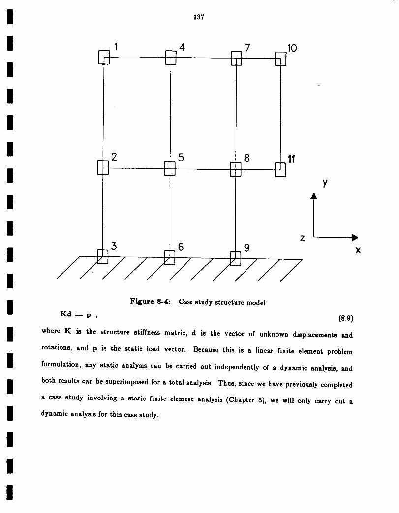
137
I 4
IZj E] L
2
-] [5
] [
7 I0
J []
] D
Z
Y
X
Figure 8-4: Ca_e study structure model
Kd ffi p , (8.9)
where K is the structure stiffness matrix, d is the vector of unknown displacements and
rotations, and p is the static load vector. Because this is a linear finite element problem
formulation, any static analysis can be carried out independently of a dynamic analysis, and
both results can be superimposed for a total analysis. Thus, since we have previously completed
a case study involving a static finite element analysis (Chapter 5), we will only carry out a
dynamic analysis for this case study.
138
8.4.1 Linear Dynamic Analysis
Dynamic analysis 35 of the structure in Figure 8-4 requires solution of the matrix equation
Mci + Cd + Kd ---- p(t) (8.10)
A consistent mass matrix M is used in the analysis, and thus it has the same structure as the
stiffness matrix K, as does the damping matrix C. Earlier, we reported that we would do the
analysis without damping 31. However, as the problem formulation progressed, the decision was
made to include damping to yield more realistic results. The vector p(t) is a vector of time-
varying loads, and ci, cl and d are the acceleration, velocity, and displacement vectors,
respectively. We consider a linear analysis, i.e. the mass, damving, and stiffness matrices remain
constant throughout the problem solution.
In our dynamic analysis, we will investigate the response of the structure to earthquake
loadings. In such an analysis, the ground nodes cannot be constrained, as the earthquake is
imparting forces and causing displacements, velocities, and accelerations at those nodes. Thus,
boundary conditions are not applied in a conventional manner, and a different approach is used
for the analysis, which is explained below.
An earthquake transfers energy from the movement of the earth to a structure, and the
actual loading forces at the ground points depend on the structure and are not known a priori.
Thus, an earthquake analysis is not usually performed by applying time-varying loads to the
ground nodes of a structure. Instead, the time-histories of the displacements, velocities, and
accelerations of the nodes due to an earthquake are prescribed from experimental and/or
theoretical data. From this information, the movements of the other nodes in the structure are
calculated.
We consider the general case where the ground nodes do not move uniformly, and set up
the problem as follows. The nodal acceleration, velocity, displacement, and load vectors of
139
equation (8.10)are written in two partitions.The top partitionof the vectors are those nodes
where the accelerations,velocities,and displacements are unknown (not prescribed),and any
staticor time-varying loads are known. The bottom partitionof the vectors consistsof the
nodes where the accelerations,velocities,and displacements are prescribed,and the nodal loads
or forcesare unknown. This partitioningofthe matrix equation isillustratedbelow,
M,dl ,.l'LC, ,,where block row 1 is the partition of nodes with unknown accelerations velocities, displacements,
and known loads, and block row 2 k the partition of nodes with prescribed accelerations
velocities,displacements and unknown loads. The corresponding partitionsof the mass,
damping, and stiffnessmatrices are as indicated.To obtainthe partitioning,rows of the original
matrix equation are simply switched.
The first equation of (8.11) is now rearranged to yield the following matrix equation
Mll¢il "_"CllCil + Klldl _ Pl " M12d2 - C12_12 " K12d2 ' (8.12)
where the entire right-hand side is known. For our case study, equation (8.12) has matrices of
size (24 by 24), and vectors of size (24 by 1). This matrix equation is solved for the acceleration,
and displacement vectors ¢/1' elf and d 1. If the vector of forces, P2 at thevelocity, ground
nodes is desired, we may solve for it by using the bottom equation of (8.11), once _iI _il, and d 1
are obtained.
We willsolve equation (8.12)using Newmark's directintegrationmethod. This solution
method has been detailedearlier31, and may be found in various references35. The earthquake
accelerationdata will be generated by computer, and will contain frequency components
appropriate for earthquake motion. The velocityand displacement data willbe obtained by
integratingthe accelerationdata. The earthquake data willsimulate an earthquake of 5 to 20
seconds in duration,and appropriatetime stepswillbe used in the Newmark algorithm. Most of
the computational effortin such an algorithmisto compute the matrix-vectormultipliesat each
time step.
140
9. OPTICAL PROCESSING EXTENSIONS
In the third year of research we intend to pursue several extensions to our optical
processing operations, including on-line arithmetic, polynomial evaluation and floating point
operations. We now discuss each of these topics.
We have recently formulated the concept for a new optical processor which implements on-
line arithmetic 36. The performance of on-line arithmetic has been shown to be superior in terms
of speed to conventional arithmetic in applications where computations are executed
......... ,; .... j , ,37wuc,,,_u_j ,_.u where pipelining may be employea On-line algorithms for addition,
subtraction, multiplication and division have been described in the literature38, 36
Conventional division is not suited to implementation in optical processors and only recursive
division algorithms have been proposed in the literature. 39. However, on-line division may be
readily implemented on our proposed on-line optical processor which also performs on-line
addition, subtraction and multiplication. This architecture represents a new approach to
numeric computations in optical processing. We will continue during the third year to
investigate our on-line arithmetic optical architecture as a fast, efficient processor of variable
precision computations. We will explore in greater detail, design requirements of the processor
to fully exploit the advantages of on-line arithmetic. The range of usefulness of our processor
can be expanded by including on-line square-root algorithms and the evaluation of vector
expressions.
Polynomial evaluation via on-line arithmetic has been proposed for digital computers 40.
We will investigate the design of the optical on-line architecure that will incorporate polynomial
evaluation as well as the aforementioned on-line algorithms, thus providing a more general-
purpose on-line optical processor.

I
II
II
II
II
III
I
II
II
II
141
A technique for implementing floating-point operations has been detailed for our optical
processor 41. This method handles the mantissa in the optical processor and the exponent in
external hardware. During the third year of research we will investigate alternative methods of
floating point implementation that may better exploit the optical nature of the processor.

142
10. SUMMARY AND FUTURE WORK
This report has described the progression of our research to date, and our remaining plans
for the third year. The bulk of that effort will be to implement the new case studies on the
existing processor and the AC-coupled version as described in Chapter 7. We also plan to
developed a new digital simulation and new error models, as discussed in our recent Research
Proposal. This will give us the ability to investigate multi-channel architectures and binary and
multi-level data encoding, and to verify their performance.

i
III
I
III
II
.
,
,
,
°
,
o
8.
,
10.
11.
12.
13.
14.
15.
16.
17.
References
B.K. Taylor and D. Casasent, "Twos-Complement Data Processing for Improved Encoded
Matrix-Vector Processors", Applied Optics, Vol. 25, 15 March 1986, pp. 961-965.
R.P. Bocker, S.R Clayton and K. Bromley, "Electrooptical Matrix Multiplication using
the Twos Complement Arithmetic for Improved Accuracy", Applied Optics, Vol. 23, July
1983, pp. 2019-2021.
A.P. Goutzoulis, "Systolic Time-Integrating Acoustooptic Binary Processor", Applied
Optics, Vol. 23, No. 22, November 1984, pp. 4095-4099.
Caroline Perlee and David Casasent, "Negative base encoding in optical linear algebra
processors", Applied Optics, Vol. 25, January 15 1986, pp. 168-169.
D. Casasent and J. Jackson, "Space and Frequency-Multiplexed Optical Linear Algebra
Processors: Fabrication and Initial Tests", Applied Optics, Vo]. 25, 15 July 1986, pp.
2258-2263.
D. Casasent and B.K. Taylor, "Banded-Matrix High-Performance Algorithm and
Architecture", Applied Optics, Vol. 24, May 1985, pp. 1476-1480.
"Special Issue on Optical Computing", Proc. IEEE, Vol. 72, No. 7, July 1984.
E. Swartzlander, "The Quasi-Serial Mutiplier", IEEE Trans. Comput., Vol. C-22, April
1973, pp. 317-321.
H.J. Whitehouse and J.M. Speiser, "Linear Signal Processing Architectures", Aspects of
Signal Processing - Part 11, G. Tacconi,ed., NATO Advanced Study Institute, Boston,
MA, 1976, pp. 669-702.
D. Psaltis, D Casasent, D. Neft and M. Carlotto, "Accurate Numerical Computation by
Optical Convolution", Proc. SPIE, Vol. 232, April 1980, pp. 151-156.
W.C. Collins, R.A. Athale and P.D. Stilwe]l, "Improved Accuracy for an Optical Iterative
Processor", Proc. SPIE, Vo]. 352, 1982, pp. 50-56.
D. Casasent, "Scene Analysis Research: Optical Pattern Recognition and Artificial
Intelligence", SPIE, Advanced Institute Series on Hybrid and Optical Computers, March
1986, Leesburg, Virginia
D. Casasent and J. Jackson, "Optical Linear Algebra Processor: Laboratory System
Performance for Optimal Control Applications", Proc. SPIE, Vol. 639, March-April 1986.
D. Casasent, J. Jackson and G. Vaerewyck, "Optical Array Processor: Laboratory
Results", Proc. SPIE, Vol. 700, IOCC 1986, Jerusalem, Israel, July 6-11 1986.
D. Casasent and A.K. Ghosh, "Optical Linear Algebra Processors: Noise and Error Source
Modeling", Optics Letters, Vol. 10, June 1985, pp. 252-254.
G.F. Carrier and C.E. Pearson, Partial Differential Equations - Theory and Technique,
Academic Press, New York, 1976, p. 262
L.A. Hagemann and D.M. Young, Applied Iteratire A4ethods, Academic Press, New York,1981.
!

II
I
III
II
18. R. Vichnetvetsky, Computer Methods for Differential Equations I, Prentice-Hall, New
York, 1981.
19. D. Casasent, A. Ghosh and C.P. Neuman, "A Quadratic Matrix Algorithm for Linear
Algebra Processors", J. Large-Scale Systems, Vol. 91985, pp. 35-49.
20. H. Carslaw and J Jaeger, Conduction of Heat in Solids, Clarendon Press, Second
Edition,Oxford, 1959.
21. D. Casasent and J. Jackson, "Real-Time Optical Laboratory Linear Algebra Solution of
Partial Differential Equations", Proc. SPIE, Vol. 698, August 1986.
22. D. Casasent and J. Jackson, "Laboratory Optical Linear Algebra Processor for Optimal
Control", Optics Communications, Vol. 60, 15 October 1986, pp. 1-4.
23. J. Fisher, D. Casasent and C.P. Neuman, "Factorized Extended Kalman Filter for Optical
Processing", Applied Optics, Vol. 25, 15 May 1986, pp. 1615-1621.
24. D. Casasent and C. Perlee, "Bipolar Biasing in High-Accuracy Optical Linear Algebra
Processors", Applied Optics, Vol. 25, 1 April 1986, pp. 1033-1035.I
25. B.K. Taylor and D. Casasent, "Error-Source Effects in a High-Accuracy Optical Finite-
Element Processor", Applied Optics, Vol. 25, 15 March 1986, pp. 966-975.
26. AUGAT, "Flight Manual Designer's Guide", Manufacturers literature, 40 Perry Ave.,
Attleboro, MA, 1985, High speed Wire-Wrap designer's guide
27. TRW LSI Products Division, VLSI Data Book, TRW Inc. La Jolla, CA 92038, P.O. Box
2472, 1984, Pages 101-112
28. Honeywell, "HDAC34010 Triple 4-bit, high speed raster D/A converter", Datasheet, 1150
Cheyenne Mountain Blvd. Colorado Springs, CO 80906, 1985.
29. K. Kawano and O. Mitomi, "Coupling characcteristics of laser diode to multimode fiber
using seperate lens method", Applied Optics, Vol. 25, No. 1, January 1986, pp. 136-141.
30. M. Sochacka, J. Sochacki and C. Gomez-Reino, "Paraxial region index profiles of GRIN
rods", Applied Optics, Vol. 25, No. 1, January 1986, pp. 142-145.
31. D.P. Casasent, B. K. Taylor, C. Perlee - Carnegie Mellon University, "Parallel Optical
Finite Element and Computational Fluid Dynamics Processors", Tech. report, Nasa
Langley Research Center, March 1987.
32. Dr. Janet Peterson, University of Pittsburgh, PA.. Information obtained through oraldiscussion
33. R.E. Smith, A. Kidd, Numerical Studies Of Incompressible Viscous FTow In A Driven
Cavity, NASA Langley Research Center, Washington, D.C., 1975, pp. 61-82, ch. 6.
34. J.S. Przemieniecki, Theory of Matrix Structural Analysis, McGraw-Hill, New York,1968.
35. K.J. Bathe and E. L. Wilson, Numerical Methods in Finite Element Analysis, Prentice-
Hall, Inc., Englewood Cliffs, New Jersey, 1976.
I
I
II
II
II
iI
II
II
II
II
II
86.
87.
38.
89.
40.
41.
M.J. Irwin, An Arithmetic Unit For On-Line Computation, PhD dissertation, University
of Illinois at Urbana-Champaign, May 1977, Report No. UIUCDCS-R-77-873
M.D. Ercegovac, "On the performance of on-line arithmetic", Proc. 1980 International
Conference on Parallel Processing, 1980, pp. 55-62.
K.S. Trivedi and M.D. Ercegovac, "On-line algorithms for division and mtiltiplication",
IEEE Trans. on Computers, Vol. c-26, July 1977, pp. 681-687.
H. John Caulfield, "Application of optical pipelines to root searching and to division",
Applied Optics, Vol. 23, Feb. 1984, pp. 373-376.
M.D. Ercegovac, "A general hardware-oriented method for evaluation of functions and
computations in a digital computer", IEEE Trans. on Computers, Vo]. C-26, July 1977,
pp. 667-680.
J. Fisher, Extended Kalman Filter Algorithms for implementation on a High-Accuracy
Optical Processor, Carnegie-Mellon Univ., Pittsburgh, Pa., December, 1984, Masters
Thesis.

143
I. POST-DETECTION HARDWARE DESIGN
1.1 Introduction
This Appendix discusses the hardware and/or software that could be used with the output
detectors of the multichannel OLAP, to implement a higher level radix (radix _> 2) or a negative
radix. We do not plan to use hardware but will use software/hardware for cost reasons. We do
not detail here the software procedure as it is straight forward. Instead, we concentrate on the
real-time hardware to demonstrate its feasibility. The extra hardware required (beyond what we
presently plan to implement) would convert the mixed radix detector output into a binary word,
so that this may be fed directly back into the controlling microprocessor. If this output is to be
re-used as a multi-level input to the OLAP on the next cycle, as in various recursive algorithms,
a D/A conversion will produce a higher-level encoding of the output binary word to the optical
processor's input. In the existing laboratory OLAP, the input operands are encoded in
conventional binary. In this case, simple shift/add hardware converts the mixed radix output
b_ck into binary. When a negative base encoding is used, or, when the radix is positive but not
a power of 2, e.g., radix_3 or radix_5, then this simple shift procedure is not sufficient and we
must resort to a slightly more complex shift/add procedure. The algorithms that define these
procedures are detailed in Section 1.2. Several modified OLAP detection systems are presented
in Section 1.3. These designs are presented as possible future modifications to the existing
detection system but will not be implemented in the laboratory. The existing detection system
will be used. Conclusions and a summary are presented in Section 1.4.
1.2 Basic OLAP output hardware
We begin by looking at the existing laboratory OLAP to show that the existing "back-
end _ is insufficient for handling negative radices and higher-level radices and that additional
hardware will be needed in order to convert the mixed-negative-radix output into a binary word.
!

144
The same inadequacy holds for radices that are not a power of two, e.g. radix---=3 or radix-----5.
Figure I-1 shows a schematic of the current post-detection electronics.
C i
i
i
III
II
Figure Ll: OL.a_P output configuration
Whether the OLAP is running in single- or multi-channel mode, positive or negative radix, the
values from the N detectors of Fig. I-1 will be mixed radix, i.e. the values on the detectors may
be greater than the radix magnitude. Every T1, these mixed radix digits are A/D converted into
a 6-bit binary word. Each 6-bit word is then added to the ECL register directly beneath each
A/D (Fig. I-1). The contents of each ECL register are then shifted to the register at its right.
The rightmost ECL register of Fig. I-1 shifts its contents (an 8 to 12 bit binary word labeled c i
in Fig. I-1) out as output. This ci is a valid digit of the VIP result. Each ci is output in bit-
parallel format. The A/D-ECL combination hardware simulates a CCD shift register by adding
successive A/D output data to prior accumulated and shifted output data in the ECL registers.
In the next T 1 cycle, new incident light is detected by the N detectors and the process is
repeated. One valid binary word, ci, is output from the rightmost register (Fig. I-1) every T 1.
In other words, binary word co is output at time t_---T1, then c I is output at t=2T1, c2 is output
at t--_--3T1, and so on. Each binary c i is an 8 to 12 bit word and all the c i combine to form the
final output, which we will assume to be the scalar Z of the OLAP input data, as given by
Z__.--.N-1 i_-Ji-----0cir ' (I.1)
where r is the encoding radix of the OLAP input data and N is the number of bits in the input
operands and also the number of detectors, A/Ds and ECL registers. The c i words are produced
I

145
II
II
III
I
II
II
I
sequentially, i.e. one every TI, and the N least-significant digits of the Z are produced after time
t-_-NXT 1. The product of two N-bit operands is a 2N-bit mixed-radix word. However, we
retain only the N least-significant digits from the detector plane. If any of the N-1 digits
remaining in the ECL registers after time t--NxT 1 are nonzero, this is treated as overflow and Z
is set to its maximum possible value, rN-1, where r is the encoding radix. This Appendix
describes the hardware/software that will convert the N ci words into a binary representation
(one word) of the scMar Z. With Z in binary form, it can be used directly as input to the
controlling microprocessor, or to a D/A convertor to generate a base r encoding of Z (for
multilevel encoding of the OLAP).
There are two cases which we considered in the hardware design:
1. the encoding radix of the operands is positive or negative and is a power of 2, i.e.
radix_---=l=(2) k, where k_l is conventional binary.
2. the encoding radix of the operands is positive or negative and is not a power of 2,
e.g., radixeS3, or radix_+5.
1.2.1 Case 1: radix is positive or negative and a power of 2
The first case is the simpler of the two cases to implement in hardware (in software, both
cases are relatively simple to implement). In this case, the mixed-radix-to-binary conversion of
the output c i words is performed by simple shift/add/subtract combination hardware. The
block diagram of Fig. I-2 illustrates the concept when the encoding radix is positive. Every T1,
the newest m-bit binary word ci from the output of Fig. I-1 (m is 8 to 12 bits in the laboratory
system) is loaded into the shift/add block in bit-parallel form. The subtract operation is not
needed for positive radices and thus is not shown. We illustrate with the example shown to the
right in Fig. I-2 where the OLAP encoding radix is binary, and N_4, i.e., the OLAP's input
operands are @bit binary words, and the binary output words from the OLAP back-end of Fig.
I-1 are c0_---0001(2), c1_-_-0010(2), c2_---0011(2 ) and c3---_0100(2 ). (These were chosen arbitrarily for
I
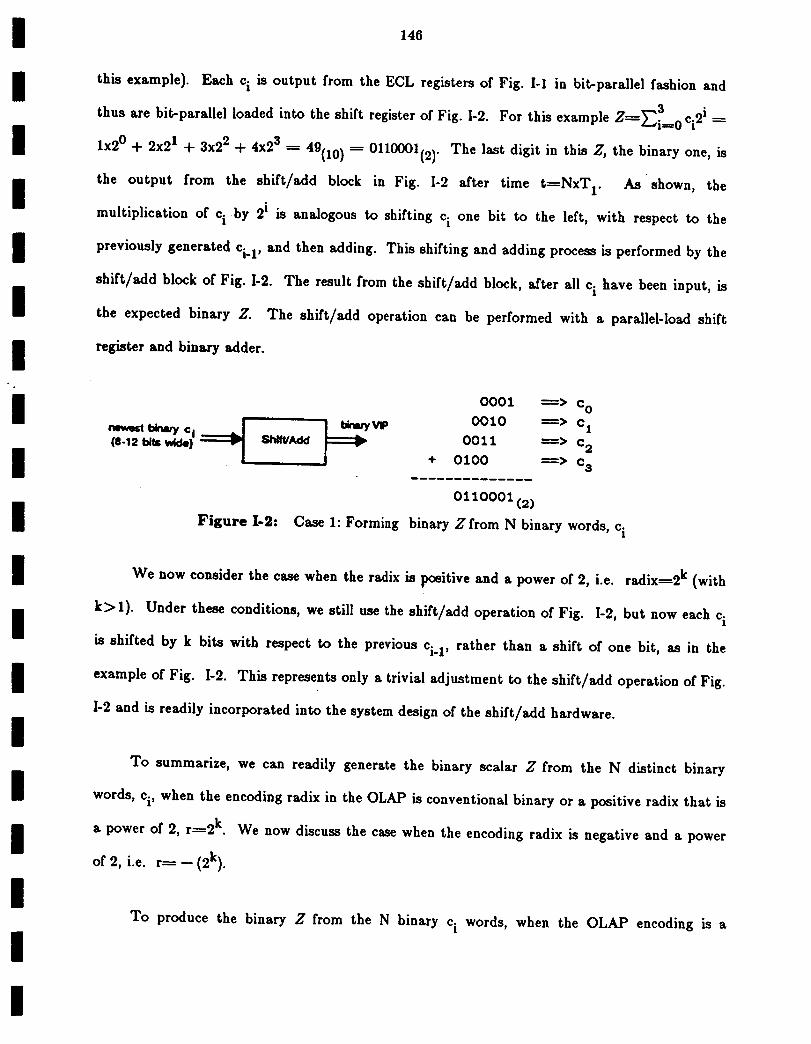
I 146
III
!
I
this example). Each ci is output from the ECL registers of Fig. bl in bit-parallel fashion and
3thus are bit-parallel loaded into the shift register of Fig. I-2. For this example Z---_>-_i= 0 ci21 -----
Ix20 + 2x21 + 3x22 + 4x23 _ 49(10) -----0110001(2 ). The last digit in this Z, the binary one, is
the output from the shift/add block in Fig. ]-2 after time t_NxT I. As shown, the
multiplication of c i by 2 i is analogous to shifting c i one bit to the left, with respect to the
previously generated Ci.l, and then adding. This shifting and adding process is performed by the
shift/add block of Fig. I-2. The result from the shift/add block, after all ci have been input, is
the expected binary Z. The shift/add operation can be performed with a parallel-load shift
I register and binary adder.
I
I
I Figure I-2: Case 1: Forming
+
0001 ---> co
0010 => cI
0011 --> c2
0100 --> ca
0110001(2 )
binary Zfrom N binary words, c i
II
II
III
I
We now consider the case when the radix is positive and a power of 2, i.e. radix=2 k (with
k>l). Under these conditions, we still use the shift/add operation of Fig. I-2, but now each ci
is shifted by k bits with respect to the previous ci.1, rather than a shift of one bit, as in the
example of Fig. I-2. This represents only a trivial adjustment to the shift/add operation of Fig.
I-2 and is readily incorporated into the system design of the shift/add hardware.
To summarize, we can readily generate the binary scalar Z from the N distinct binary
words, ci, when the encoding radix in the OLAP is conventional binary or a positive radix that is
power of 2, r-_-2 k. We now discuss the case when the encoding radix is negative and _ power
of 2, i.e. r-- -- (2k).
To produce the binary Z from the N binary c i words, when the OLAP encoding is a
I

147
negative base, the shift/add operation also requires a subtraction. To illustrate, we expand (I.1),
for the case r-_-- (2k), into binary form and let the binary c i be c0-_-0001(2), c1-_-0010(2),
c2-----0011(2 ) and c3_--0100(2), as in the previous example. Also, let the encoding radix of the
OLAP be negabinary, i.e. r_ -- 2. Hence, we express (I.1) as
3Z = _i=O ci(- 2)i" (I.2)
As in the previous examples corresponding to a positive radix, (I.2) must be expressed in binary
form because the shift/add/subtract hardware is binary-based. Thus, we expand (I.2) as
3 ___Z _-- _"_i----Oci( -- 2)i CoX('2)O + CLX('2)1 -t- c2x(-2)2 + c3x(-2)3
= c0x(20 ) -- ClX(2i ) + C2x(22) -- c3x(23) . (I.3)
The last line of (I.3) is analogous to the example at the right of Fig. I-2, except that the outputs
c i are alternately added and subtracted in (I.3). The amount of shift for each ci in (I.3) is the
same as in Fig. I-2. Therefore, when the encoding radix is positive, the c i are shifted and added.
When the encoding radix is negative, the ci are shifted and alternately added and subtracted.
Thus, the digital hardware realization of these shift/add algorithms has been designed to allow
both positive and negative radix encoding, by employing a binary adder/subtractor or ALU in
the circuit.
1.2.2 Case 2: Radix is positive or negative and not a power of 2
The simple shift and add algorithm of Fig. I-2 is not applicable when the radix is not a
power of 2, e.g., when r---_-1-3 or r-_--I-5. In this case, in order to convert the N ci words into the
binary scalar Z, multiple shifts and adds must be performed on each ci. By comparison, when
r_--2 k, only one shift (of k bits) is necessary for each ci before it is added to the sum of the prior
outputs. We illustrate with an example. Consider the case when the encoding radix is r_3. As
in the example of Fig. I-2, we arbitrarily let the ci words be c0_0001(2), c1_0010(2), c2_0011(2 )
and c3-----0100(2 ). Note that the ci are binary, not base 3. No attempt has been made to alter
the hardware design of Fig. I-l, which already exists in the laboratory set-up.

II
II
II
III
II
II
II
II
I
148
The scalar Z, as defined by (I.1), is
Z ffi _"_0 ci 3i ffi c0xl + ClX3 -k c2x9 q- c3x27. (].4)
Recall that each ci is an 8 to 12 bit binary word. As in the previous examples, we express (I.4)
in binary base since the shift/add/subtract hardware is binary based, thus
Z _ _"_d--0 ci31 _ c0xl -F clx31 -k c2x32 + c3x33, (I.5)
c0x20 + ClX(20q-21) + c2x(20+23 ) + c3x(20+21-k23+24). (1.6)
Equation {I.e) is obtained from (].5) by replacing the base +2 representation for 3 i in (I.5).
Equations {1.5) and (I.6) are equivalent, except that (I.6) is directly implementable in digital
shift/add hardware in a manner similar to the example of Fig. 1-2. In other words, (I.6) is a sum
of cix2J terms, and each cix2J can be produced by shifting ci by j bits to the left {of its LSB). Let
us now detail the shift and add realization of (1.6). In the first term, the multiplier 20 of Co,
indicates that no shift is performed on e0. To this c0x20 term we add the term CLX(20+21),
which is produced by shifting c I by 0 bits (i.e. unshifted) and adding that to cI shifted by 1 bit.
Proceeding similarly, appropriate shifts and adds on each of the ci will produce the binary Z for
R_3. Figure I-3 illustrates the corresponding shifts and adds necessary to produce the ,7 result
in (L6).
÷
0001
001_
0010
0011
0011
0100-0100
0100
0100
co (20 )
c z (20+2 I)
co.(2°+2 s)
C3 (20+21+23+24 )
1 0 0 0 1 1 1 0(2 ) = Z(_.)
Figure L3: Shift/Add procedure when R=3
The method used in expanding the Z of (I.5) into the binary form of (I.6) can be
generalized to any positive radix. Figure I-4 shows the binary expansion of a scalar ,7 for OLAP
I
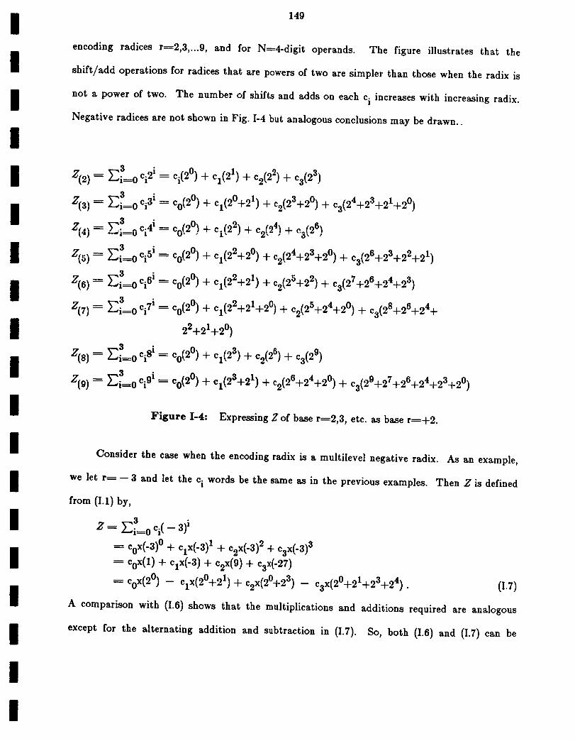
149
encoding radices rR2,3,...9, and for N---_4-digit operands. The figure illustrates that the
shift/a_ld operations for radices that are powers of two are simpler than those when the radix is
not a power of two. The number of shifts and adds on each ci increases with increasing radix.
Negative radices are not shown in Fig. I-4 but analogous conclusions may be drawn..
_--- _i-----0 ci21 = Ci(20) + Cl(21) + c2(22) + c3 (23)zC2) 3
Z{3 ) ---_ _30 ci31 _--_-C0(20) + C1(20+21) + c2(23+20) + c3(24+23+21+20)
Z_,, _--- _-,3 .. C.41 _ C0(20_ + Ci(22) -_ c2(24) -4- c3(26 )
Z(5) = _---0 ci5' = c0 (20) + c1(22+20) + c2(24+23+20) + c3 (26+23+22+21)
Z(6) = _0 ci61 = c0(20) + Cl (22+21) + c2(25+22) + c3(27+26+24+23)
Z(7) = _"_0 ci71_- c0(20) + Cl(22+21+20) + c2 (25+24+20) + c3 (28+26+24+
22+21+20 )
2'(8) = _i=03 ci81"= c0(20) + c1(23) + c2(26) + c3(29)
3Z(9) = _'_iffi0 cigZ ffi c0(20) + Cl (23+21) + c2(26+24+20) + c3(29+27+26+24+23+20)
Figure L4: Expressing Z of base r_---2,3, etc. as base r_+2.
Consider the case when the encoding radix is a multilevel negative radix. As an example,
we let r_ -- 3 and let the c i words be the same as in the previous examples. Then Z is defined
from (I.1) by,
3Z ---_ _"_i=0 ci( -- 3)i
_--- c0x(-3)0 + CLX(-3)1 + c2x(-3)2 + c3x(-3)3
c0x(1 ) + ClX(-3 ) + c2x(9) + c3x(-27 )
_- c0x(20) -- CLX(20+21) + c2x(20+23) -- c3x(20+21+23+24) . (I.7)
A comparison with (1.6)shows that the multiplicationsand additions required are analogous
except for the alternatingaddition and subtractionin (1.7). So, both (1.6)and (1.7)can be

II
II
II
II
III
II
I
III
I
150
implemented with the same hardware employing a binary adder/subtractor or ALU to handle
the addition and subtraction. Calculations have shown that the speed of this conversion circuit
is too slow to operate efficiently with the OLAP when the radix is not a power of 2. Therefore,
we plan to implement the shift/add/subtract hardware and employ only radices that are powers
of 2, and either positive or negative. We expect no loss in processing capability from this
decision. The shift/add/subtract unit is implemented with the OLAP detection system as shown
in Fig. I-5.
O0 0
Figure I-5: OLAP detection system and conversion unit
1.3 Future OLAP Detection Systems
The post-detection circuitry of Fig. I-1 has been constructed on the laboratory OLAP and
will be used with all the tests conducted on the system. However, we propose several alternative
designs to the post-detection circuitry to reduce its complexity while maintaining reasonable
dynamic range requirements. Two of these alternatives are presented below.
The post-detection circuitry of Fig. I-5 relies on the future availability of Ga.A.s CCD
analog shift registers. This design requires only one A/D. However, the dynamic range
requirements are increased from that of Fig. I-1. The system of Fig. I-5 operates at the same
throughput rate as the system of Fig. I-1. Every T1, the rightmost, or current least significant,
I
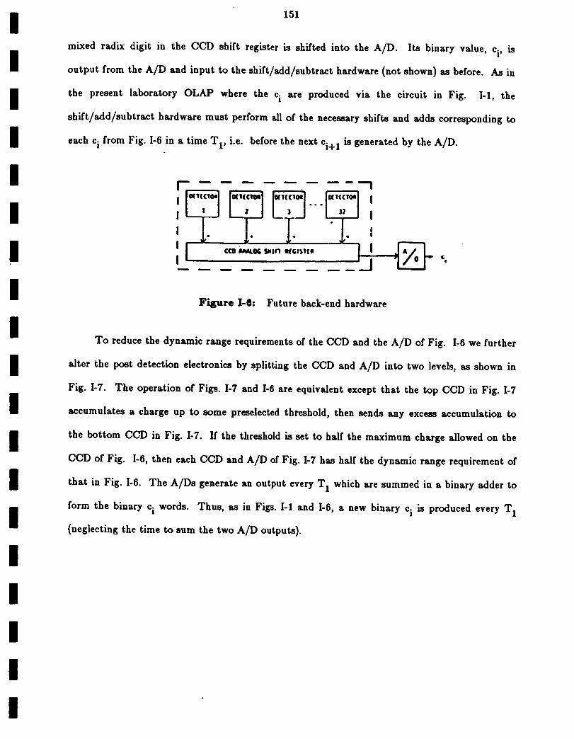
I 151
mixed radix digit in the CCD shift register is shifted into the A/D. Its binary value, ci, is
I output from the A/D and input to the shift/add/subtract hardware (not shown) as before. As in
I the present laboratory OLAP where the c i are produced via the circuit in Fig. I-l, the
shift/add/subtract hardware must perform all of the necessary shifts and adds corresponding to
I each ci from Fig. I-6 in a time T1, i.e. before the next ci+ 1 is generated by the A/D.
,i / / ° _ i
l- ].. J.- _L- '
IFigure ][-6: Future back-end hardware
III
To reduce the dynamic range requirements of the CCD and the A/D of Fig. I-6 we further
alter the post detection electronics by splitting the CCD and A/D into two levels, as shown in
Fig. I-7. The operation of Figs. I-7 and I-6 are equivalent except that the top CCD in Fig. I-7
accumulates a charge up to some preselected threshold, then sends any excess accumulation to
I
I
the bottom CCD in Fig. I-7. If the threshold is set to half the maximum charge allowed on the
CCD of Fig. I-6, then each CCD and A/D of Fig. I-7 has half the dynamic range requirement of
that in Fig. I-6. The A/I)s generate an output every T 1 which are summed in a binary adder to
I form the binary c i words. Thus, as in Figs. I-1 and I-6, a new binary c i is produced every T 1
(neglecting the time to sum the two A/D outputs).
I
I
I
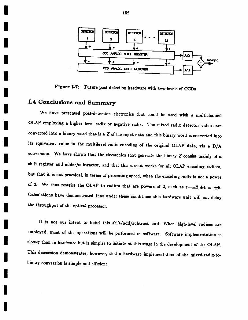
I
II
III
II
II
III
II
II
I
152
Figure Io7: Future post-detection hardware with two-levels of CCI)s
1.4 Conclusions and Summary
We have presented post-detection electronics that could be used with a multichannel
OLAP employing a higher level radix or negative radix. The mixed radix detector values are
converted into a binary word that is a Z of the input data and this binary word is converted into
its equivalent value in the multilevel radix encoding of the original OLAP data, via a D/A
conversion. We have shown that the electronics that generate the binary Z consist mainly of a
shift register and adder/subtractor, and that this circuit works for all OLAP encoding radices,
but that it is not practical, in terms of processing speed, when the encoding radix is not a power
of 2. We thus restrict the OLAP to radices that are powers of 2, such as r-----4-2,+4 or 4-8.
Calculations have demonstrated that under these conditions this hardware unit will not delay
the throughput of the optical processor.
It is not our intent to build this shift/add/subtract unit. When high-level radices are
employed, most of the operations will be performed in software. Software implementation is
slower than in hardware but is simpler to initiate at this stage in the development of the OLAP.
This discussion demonstrates, however, that a hardware implementation of the mixed-radix-to-
binary conversion is simple and efficient.
I


![Lifestyle of Success eZine [v01 i01]](https://static.fdocuments.us/doc/165x107/577dac2e1a28ab223f8d86d8/lifestyle-of-success-ezine-v01-i01.jpg)