ACTgen Cores Reference Guide - actel.kr Brent-Kung Adder extends the ranges ... • Optional...
208
ACTgen Cores Reference Guide
Transcript of ACTgen Cores Reference Guide - actel.kr Brent-Kung Adder extends the ranges ... • Optional...
ACTgen Cores Reference Guide

Table of Contents
2 ACTgen Cores Reference Guide
Actel Corporation, Sunnyvale, CA 94086
© 2004 Actel Corporation. All rights reserved.
Part Number: 5029108-11
Release: September 2004
No part of this document may be copied or reproduced in any form or by any means without prior written consent of Actel.
Actel makes no warranties with respect to this documentation and disclaims any implied warranties of merchantability or fitness for a particular purpose.
Information in this document is subject to change without notice. Actel assumes no responsibility for any errors that may appear in this document.
This document contains confidential proprietary information that is not to be disclosed to any unauthorized person without prior written consent of Actel Corporation.
TrademarksActel and the Actel logotype are registered trademarks of Actel Corporation.
Acrobat Reader is a trademark of Adobe Systems, Inc.
Windows is a registered trademark of Microsoft in the U.S. and other countries.
All other products or brand names mentioned are trademarks or registered trademarks of their respective holders.

Table of Contents
Introduction . . . . . . . . . . . . . . . . . . . . . . . . . . . . . 5Document Conventions . . . . . . . . . . . . . . . . . . . . . . . . . . . . . . . 5
Symbols . . . . . . . . . . . . . . . . . . . . . . . . . . . . . . . . . . . . . . . 6
Your Comments . . . . . . . . . . . . . . . . . . . . . . . . . . . . . . . . . . . 6
Online Help . . . . . . . . . . . . . . . . . . . . . . . . . . . . . . . . . . . . . 6
1 Arithmetic Cores . . . . . . . . . . . . . . . . . . . . . . . . . . 7Advanced Options . . . . . . . . . . . . . . . . . . . . . . . . . . . . . . . . . 34
2 Comparators . . . . . . . . . . . . . . . . . . . . . . . . . . . . 39
3 Converters . . . . . . . . . . . . . . . . . . . . . . . . . . . . . . 45
4 Counters . . . . . . . . . . . . . . . . . . . . . . . . . . . . . . 51
5 Decoder . . . . . . . . . . . . . . . . . . . . . . . . . . . . . . . 59
6 I/Os . . . . . . . . . . . . . . . . . . . . . . . . . . . . . . . . . 63
7 Logic . . . . . . . . . . . . . . . . . . . . . . . . . . . . . . . . 81
8 Multiplexer . . . . . . . . . . . . . . . . . . . . . . . . . . . . . 85
9 Minicores . . . . . . . . . . . . . . . . . . . . . . . . . . . . . . 89
10 PLLs . . . . . . . . . . . . . . . . . . . . . . . . . . . . . . . . 99Functionality . . . . . . . . . . . . . . . . . . . . . . . . . . . . . . . . . . . 108
Configure Clock Conditioning / PLL cores . . . . . . . . . . . . . . . . . . . 109
11 Register (Storage Elements) . . . . . . . . . . . . . . . . . . . 115
12 Memory Cores for Non-Axcelerator Families 129
ACTgen Macros Reference Guide 3

Table of Contents
13 Memory Cores for Axcelerator . . . . . . . . . . . . . . . . . . 155
14 Memory Cores for ProASIC, ProASICPLUS, and ProASIC3/E Devices 165
A Memory in ProASIC and ProASICPLUS . . . . . . . . . . . . . 185Embedded Memory . . . . . . . . . . . . . . . . . . . . . . . . . . . . . . . 185
Distributed Memory . . . . . . . . . . . . . . . . . . . . . . . . . . . . . . . 190
Timing for Distrubuted Memories . . . . . . . . . . . . . . . . . . . . . . . 196
Using Multiple Memories in a Design . . . . . . . . . . . . . . . . . . . . . 199
B Product Support . . . . . . . . . . . . . . . . . . . . . . . . . . 207Customer Service . . . . . . . . . . . . . . . . . . . . . . . . . . . . . . . . 207
Actel Customer Technical Support Center . . . . . . . . . . . . . . . . . . . 207
Actel Technical Support . . . . . . . . . . . . . . . . . . . . . . . . . . . . . 207
Website . . . . . . . . . . . . . . . . . . . . . . . . . . . . . . . . . . . . . 207
Contacting the Customer Technical Support Center . . . . . . . . . . . . . . 208
4 ACTgen Macros Reference Guide

Introduction
This guide provides descriptions of cores that you can generate using the Actel ACTgen core builder software. For more information about instantiating cores, refer to the Actel HDL Coding Style Guide and the ACTgen online help.
The Actel ACTgen core builder generates a large variety of commonly used functions. You can generate structural netlists in EDIF, VHDL, and Verilog. Furthermore, you can generate VHDL and Verilog behavioral models for most parameterized functions (the behavioral models may be used in a simulation environment).
Actel’s parameterized cores:
• Reduce the development time of complex functions.
• Offer a large set of implementations for each type of function.
• Offer a wide range of bit widths that provides a quick change of design definitions.
Document ConventionsThe following table describes the conventions that are used throughout this manual.
Table 1. Functional Description of Table Nomenclature
Symbol Definition
X Don’t care
1 Logical 1 or high
0 Logical 0 or low
¦ Rising edge
Ø Falling edge
Qn Value of the signal Q before the active edge of the clock
Qn+1 Value of the signal Q after the active edge of the clock
Qn [width-1 : 0]
Qn is a width-bit bus
Qn [width-1 Width-1 bit of Qn
ACTgen Cores Reference Guide 5
Introduction
SymbolsEach core symbol shows the input and output ports. Busses are highlighted with a bold line; scalar signals with a thin line. The actual symbols generated by ACTgen could look slightly different, depending on the particular CAE tool used. Some ports shown could be optional, as described in the port description tables. Default polarities are shown on the symbols.
Your CommentsActel Corporation strives to produce the highest quality online help and printed documentation. We want to help you learn about our products, so you can get your work done quickly. We welcome your feedback about this guide and our online help. Please send your comments to [email protected].
Online HelpThe Designer software comes with online help. Online help specific to each software tool is available in Libero, Designer, ACTgen, ACTmap, Silicon Expert, Silicon Explorer II, and Silicon Sculptor. Please refer to the ACTgen online help (open ACTgen and from the Help menu, select ACTgen Help) for a complete explanation of how to use the ACTgen tool.
m, n Binary pattern with width of function
Table 1. Functional Description of Table Nomenclature (Continued)
Symbol Definition
6 ACTgen Cores Reference Guide

1Arithmetic Cores
ACTgen Cores Reference Guide 7

Adder
Features• Parameterized word length
• Optional carry-in and carry-out signals
• Multiple gate-level implementations (speed/area tradeoffs)
• Behavioral simulation model in VHDL and Verilog
Family SupportACT 1, ACT 2/1200XL, ACT 3, 3200DX, 40MX, 42MX, 54SX, 54SX-A, eX, 500K, PA, 500K, Axcelerator, ProASIC3/E
Description
Cin
Sum
Cout
DataA
DataB
Table 1-1. Port Description
Port Name Size Type Req/Opt Function
DataA WIDTH Input Req. Input Data
DataB WIDTH Input Req. Input Data
Cin 1 Input Opt. Carry-in
Sum WIDTH Output Req. Sum
Cout 1 Output Opt. Carry-out
Table 1-2. Parameter Description
Parameter Family Value Function
WIDTHa
500K, PA 2-128
Word length of DataA, DataB and SumAxcelerator 2-156
Other 2-32
MAXFANOUT 500K, PA0 Automatic choice (function of WIDTH)
2-16 Manual setting of Max. Fanout
CI_POLARITY ALL 0 1 2 Carry-in polarity (active high, active low and not used)
ACTgen Cores Reference Guide 8

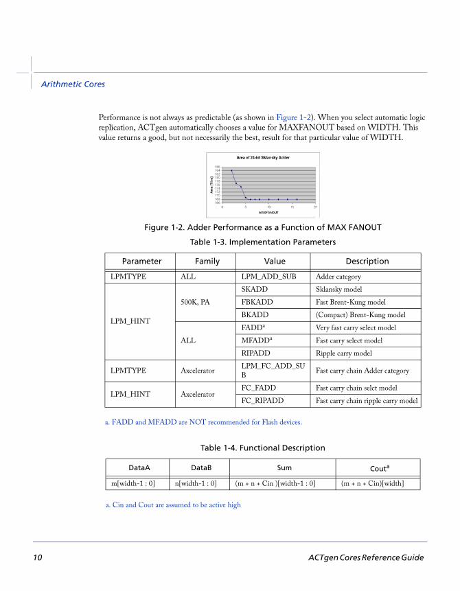
The Sklansky Adder enables you to un-check the Automatic Max. Fanout box and specify a value for max fanout. This makes ACTgen perform logic replication on high fanout nets so that the maximum fanout for all the nets in the design is not more than the value specified. If it is set to automatic, ACTgen automatically makes the decision for logic replication based on the size of the design.
The MAXFANOUT parameter enables you to perform logic replication for all Flash Adders, Subtractors, Adder/Subtractors and Accumulators. Inherently only the Sklansky algorithm generates high-fanout nets (max. fanout = WIDTH/2), so you will see effects only for this algorithm. The area increases exponentially for MAXFANOUT approaching 2 and it flattens out for higher values, as shown in Figure 1-1.
Figure 1-1. Adder Area as a Function of MAX FANOUT
CO_POLARITY ALL 0 1 2 Carry-out polarity (active high, active low and not used)
a. The Brent-Kung Adder extends the ranges from 32 to 128 bit for 54SX, 54SX-A and from 20 to 128 bit
for 500K
Table 1-2. Parameter Description
Parameter Family Value Function
ACTgen Cores Reference Guide 9
Arithmetic Cores
Performance is not always as predictable (as shown in Figure 1-2). When you select automatic logic replication, ACTgen automatically chooses a value for MAXFANOUT based on WIDTH. This value returns a good, but not necessarily the best, result for that particular value of WIDTH.
Figure 1-2. Adder Performance as a Function of MAX FANOUT
Table 1-3. Implementation Parameters
Parameter Family Value Description
LPMTYPE ALL LPM_ADD_SUB Adder category
LPM_HINT
500K, PA
SKADD Sklansky model
FBKADD Fast Brent-Kung model
BKADD (Compact) Brent-Kung model
ALL
FADDa
a. FADD and MFADD are NOT recommended for Flash devices.
Very fast carry select model
MFADDa Fast carry select model
RIPADD Ripple carry model
LPMTYPE AxceleratorLPM_FC_ADD_SU
BFast carry chain Adder category
LPM_HINT AxceleratorFC_FADD Fast carry chain selct model
FC_RIPADD Fast carry chain ripple carry model
Table 1-4. Functional Description
DataA DataB Sum Couta
a. Cin and Cout are assumed to be active high
m[width-1 : 0] n[width-1 : 0] (m + n + Cin )[width-1 : 0] (m + n + Cin)[width]
10 ACTgen Cores Reference Guide

Array Adder
Features• Parameterized word length and number of input buses
• DADDA tree architecture with optional Final Adder
• Optional pipeline for implementation with Final Adder
• Behavioral simulation model in VHDL and Verilog
Family Support54SX, 54SX-A, eX, 500K, PA, Axcelerator, ProASIC3/E
DescriptionThe Array-Adder implements a Sum-Function over an Array of Buses:
where
In applications where designers have to add more than two operands at a time “Carry-Save- Techniques” might be used to build the final Sum. ACTgen makes these techniques available through the Array-Adder core, which is using a Dadda tree algorithm. Usually this algorithm is more compact and faster than using Adder-trees consisting of multiple 2-operand adders, especially if the number of operands gets large and/or for large word width.
An example could be the FIR-filter architecture using a “distributed arithmetic” as described in the Application Note from September 1997 “Designing FIR Filters with Actel FPGAs.” This architecture generates a large number of partial products, which need to be summed up. Summing them up in an Adder-Tree would both be slow and area expensive. At the time of writing this document synthesis tools did not infer Multiple-Operand-Adders. Therefore making use of the Array-Adder in those types of applications might result in a significant gain in both speed and area.
The Array Adder comes with or without Final Adder. The version with Final Adder allows to instantiate a pipeline stage between the Dadda-tree and the Final Adder. The output bitwidth for Sum can be calculated using this formula:
OUTWIDTH = log2((m*exp2(n)-1)+1) <= n + log2(m)
The version without Final Adder has two output ports: SumA and SumB, which added together, will provide the Final Result. It is
SumA_Width <= SumB_Width <= OUTWIDTH
Data0
Data1
DataN-1
Sum!!!!
Sum Data (i)∑= i 0 to SIZE-1( )=
ACTgen Cores Reference Guide 11

Arithmetic Cores
The differences are at most one bit. This variation of the Array-Adder is particularly useful for an application, which would cascade the Array-Adder. In that case only the last stage would need a Final Adder to build the result.
Table 1-5. Port Description
Port Name
Size Type Req/Opt Function
Data0 WIDTH Input Req. Input Data (Operand 0)
Data1 WIDTH Input Req. Input Data (Operand 1)
Data2 WIDTH Input Req. Input Data (Operand 2)
Datax WIDTH Input Opt. Input Data (Operand X) X>2
Sum OUTWIDTH Output Req.
Clock 1 Input Opt. Clock (if pipelined)
Table 1-6. Parameter Description
Parameter Value Function
WIDTH width AX/Flash: 2-64All others: 2-32
Word length Data(i)
SIZE sizeAX/Flash: 3-64All others: 3-32
Number of input buses
CKL_EDGE RISE FALL Clock (if pipelined)
Table 1-7. Implementation Parameters
Parameter Value Description
LPMTYPE DADDA Generic Array Adder category
LPM_HINT ARRADD Array Adder with Final Adder
ARRADDP Pipelined Array Adder with Final Adder
ARRADD2 Array Adder without Final Adder
Data i( )∑ i 0 to SIZE-1=→
12 ACTgen Cores Reference Guide
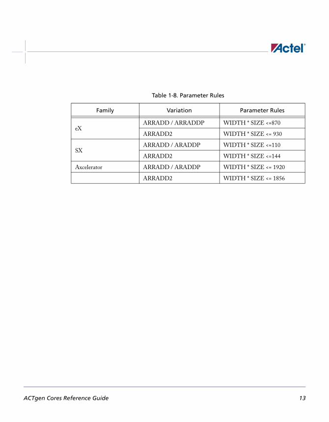
Table 1-8. Parameter Rules
Family Variation Parameter Rules
eXARRADD / ARRADDP WIDTH * SIZE <=870
ARRADD2 WIDTH * SIZE <= 930
SXARRADD / ARADDP WIDTH * SIZE <=110
ARRADD2 WIDTH * SIZE <=144
Axcelerator ARRADD / ARADDP WIDTH * SIZE <= 1920
ARRADD2 WIDTH * SIZE <= 1856
ACTgen Cores Reference Guide 13

Subtractor
Features• Parameterized word length
• Optional carry-in and carry-out signals
• Multiple gate-level implementations (speed/area tradeoffs)
• Behavioral simulation model in VHDL and Verilog
Family SupportACT 1, ACT 2/1200XL, ACT 3, 3200DX, 40MX, 42MX, 54SX, 54SX-A, eX, 500K, PA, Axcelerator, ProASIC3/E
Description
Cin
Sum
Cout
DataA
DataB
Table 1-9. Port Description
Port Name Size Type Req/Opt Function
DataA WIDTH Input Req. Input Data
DataB WIDTH Input Req. Input Data
Cin 1 Input Opt. Carry-in
Sum WIDTH Output Req. Sum
Cout 1 Output Opt. Carry-out
Table 1-10. Parameter Description
Parameter Family Value Function
WIDTHa
500K, PA 2-128
Word length of DataA, DataB and SumAxcelerator 2-156
Other 2-32
MAXFANOUT 500K, PA0 Automatic choice (function of WIDTH)
2-16 Manual setting of Max. Fanout
ACTgen Cores Reference Guide 14

CI_POLARITY ALL 0 1 2 Carry-in polarity (active high, active low and not used)
CO_POLARITY ALL 0 1 2 Carry-out polarity (active high, active low and not used)
a. The Brent-Kung Subtractor extends the ranges from 32 to 128 bit for 54SX, 54SX-A and from 20 to 128
bit for 500K
Table 1-11. Implementation Parameters
Parameter Familiy Value Description
LPMTYPE ALL LPM_ADD_SUB Subtracter category
LPM_HINT
500K, PA
SKSUB Sklansky model
FBKSUB Fast Brent-Kung model
BKSUB (Compact) Brent-Kung model
ALL
FSUBa Very fast carry select model
MFSUBa
a. FSUB and MFSUB are not recommended for Flash devices.
Fast carry select model
RIPSUB Ripple carry model
LPMTYPE Axcelerator LPM_FC_ADD_SUB Fast carry chain Subtractor category
LPM_HINT AxceleratorFC_FSUB Fast carry chain selct model
FC_RIPSUB Fast carry chain ripple carry model
Table 1-12. Functional Description
DataA DataB Sum Couta
a. Cin and Cout are assumed to be active high
m[width-1 : 0] n[width-1 : 0] (m - n - Cin) [width-1 : 0] (m - n - Cin)[width]
Table 1-10. Parameter Description (Continued)
Parameter Family Value Function
ACTgen Cores Reference Guide 15

Adder/Subtractor
Features• Parameterized word length
• Optional carry-in and carry-out signals
• Mulitiple gate-level implementations (speed/area tradeoffs)
• Behavioral simulation model in VHDL and Verilog
Family SupportACT 1, ACT 2/1200XL, ACT 3, 3200DX, 40MX, 42MX, 54SX, 54SX-A, eX, 500K, PA, Axcelerator, ProASIC3/E
Description
Cin
Sum
Cout
DataA
DataB
Addsub
Table 1-13. Port Description
Port Name Size Type Req/Opt Function
DataA WIDTH Input Req. Input Data
DataB WIDTH Input Req. Input Data
Cin 1 Input Opt. Carry-in
Sum WIDTH Output Req. Sum
Cout 1 Output Opt. Carry-out
Addsub 1 Input Req.Addition (AddSub = 1) or subtraction (Addsub = 0)
Table 1-14. Parameter Description
Parameter Family Value Function
WIDTHa
500K, PA 2-128
Word length of DataA, DataB and SumAxcelerator 2-156
Other 2-32
ACTgen Cores Reference Guide 16

MAXFANOUT 500K, PA0 Automatic choice (function of WIDTH)
2-16 Manual setting of Max. Fanout
CI_POLARITY ALL 0 1 2 Carry-in polarity (active high, active low, and not used)
CO_POLARITY ALL 0 1 2 Carry-out polarity (active high, active low, and not used)
a. The Brent-Kung Adder/Subtractor extends the ranges from 32 to 128 bit for 54SX, 54SX-A and from 20 to 128
bit for 500K
Table 1-14. Parameter Description
Parameter Family Value Function
Table 1-15. Implementation Parameters
Parameter Family Value Description
LPMTYPE ALL LPM_ADD_SUB Adder/Subtracter category
LPM_HINT
500K, PA
SKADDSUB Sklansky model
FBKADDSUB Fast Brent-Kung model
BKADDSUB (Compact) Brent-Kung model
ALL
FADDSUBa
a. FADDSUB and MFADSUBB are not recommended for Flash devices.
Very fast carry select model
MFADDSUBa Fast carry select model
RIPADDSUB Ripple carry model
LPMTYPE Axcelerator LPM_FC_ADD_SUB Fast carry chain Adder category
LPM_HINT AxceleratorFC_FADDSUB Fast carry chain selct model
FC_RIPADDSUB Fast carry chain ripple carry model
Table 1-16. Functional Description
DataA DataB Addsub Sum Couta
m[width-1 : 0] n[width-1 : 0] (m + n + Cin )[width-1 : 0] (m + n + Cin)[width] m[width-1 : 0]
m[width-1 : 0] n[width-1 : 0] (m - n - Cin) [width-1 : 0] (m - n - Cin)[width] m[width-1 : 0]
a. Cin and Cout are assumed to be active high here.
ACTgen Cores Reference Guide 17

Accumulator
Features• Parameterized word length
• Optional carry-in and carry-out signals
• Asynchronous reset
• Accumulator enable
• Multiple gate-level implementations (speed/area tradeoffs)
• Behavioral simulation model in VHDL and Verilog
Family SupportACT 1, ACT 2/1200XL, ACT 3, 3200DX, 40MX, 42MX, 54SX, 54SX-A, eX, PA, 500K, Axcelerator, ProASIC3/E
Description
DataA
Cin
Enable
Clock
Sum
Cout
Aclr
Table 1-17. Port Description
Port Name Size Type Req/Opt Function
DataA WIDTH Input Req. Input Data
Cin 1 Input Opt. Carry-in
Sum WIDTH Output Req. Sum
Cout 1 Output Opt. Carry-out
Enable 1 Input Opt Enable
Clock 1 Input Req. Clock
Aclr 1 Input OptAsynchronous Reset
ACTgen Cores Reference Guide 18

Table 1-18. Parameter Description
Parameter Family Value Function
WIDTHa
500K, PA 2-128
Word length of DataA, DataB and SumAxcelerator 2-156
Other 2-32
MAXFANOUT 500K, PA0 Automatic choice (function of WIDTH)
2-16 Manual setting of Max. Fanout
CI_POLARITY ALL 0 1 2 Carry-in polarity (active high, active low, and not used)
CO_POLARITY ALL 0 1 2 Carry-out polarity (active high, active low, and not used)
CLR_POLARITY ALL 0 1 2 Asynchronous reset (active high, active low, and not used)
EN_POLARITY ALL 0 1 2 Accumulator enable (active high, active low, and not used)
FFTYPEb ALL except FlashREGULAR
TMRFF type used (Regular, Triple Voting)
CLK_EDGE ALL RISE FALL Active High/Low
a. The Brent-Kung Accumulator extends the ranges from 32 to 128 bit for 54SX, 54SX-A and from 20 to 128 bit for
500K
b. TMR is Triple Module Redundancy. Choosing this option makes ACTgen use TMR FlipFlops that are used to
avoid Single Event Upsets (SEUs) for Rad-hard Designs. Choosing this option causes the Sequential resource usageto be tripled in families where no TMR is implemented in Silicon.
Table 1-19. Fan-in Control Parameters
Parameter Value
CLR_FANIN AUTO MANUAL
CLR_VAL <val> [default value for AUTO is 8, 1 for MANUAL]
EN_FANIN AUTO MANUAL
EN_VAL <val> [default value for AUTO is 6, 1 for MANUAL]
ACTgen Cores Reference Guide 19

Arithmetic Cores
CLK_FANIN AUTO MANUAL
CLK_VAL <val> [default value for AUTO is 8, 1 for MANUAL]
Table 1-20. Implementation Parameters
Parameter Family Value Description
LPMTYPE LPM_ADD_SUB Accumulator category
LPM_HINT
500K, PA
SKACC Sklansky model
FBKACC Fast Brent-Kung model
BKACC (Compact) Brent-Kung model
ALL
FACCa
a. The FACC and MACC parameters are not recommended for Flash devices.
Very fast carry select model
MFACCa Fast carry select model
RIPACC Ripple carry model
LPMTYPE Axcelerator LPM_FC_ADD_SUB Fast carry chain Adder category
LPM_HINT AxceleratorFC_FACC Fast carry chain selct model
FC_RIPACC Fast carry chain ripple carry model
Table 1-21. Functional Description
DataA Sumn+1 Couta
a. Cin and Cout are assumed to be active high.
m[width-1 : 0] (m + Sumn + Cin )[width-1 : 0] (m + Sumn + Cin)[width]
Table 1-19. Fan-in Control Parameters
Parameter Value
20 ACTgen Cores Reference Guide

Incrementer
Features• Parameterized word length
• Optional Carry-out signals
• One very fast gate level implementation, FC High Speed and FC Ripple available
• Behavioral simulation model in VHDL and Verilog
Family SupportACT 2/1200XL, ACT 3, 3200DX, 42MX, 54SX, 54SX-A, eX, 500K, PA, Acelerator, ProASIC3/E
Description
Sum
Cout
DataA
1
Table 1-22. Port Description
Port Name Size Type Req/Opt Function
DataA WIDTH Input Req. Input Data
Sum WIDTH Output Req. Sum
Cout 1 Output Opt. Carry-out
Table 1-23. Parameter Description
Parameter Value Function
WIDTH2-32
2-156 for FC CoresWord length of DataA and Sum
CO_POLARITY 0 1 2 Carry-out polarity (active high, active low, and not used)
ACTgen Cores Reference Guide 21

Arithmetic Cores
Table 1-24. Implementation Parameters
Parameter Value Description
LPMTYPE LPM_ADD_SUB Incrementer category
LPM_HINTFINC; FC_FINC, FC_RIPINC
Very fast carry look ahead
Table 1-25. Functional Description
DataA Sum Cout
m m + 1 (m + 1) ≥ 2width
22 ACTgen Cores Reference Guide

Decrementer
Features• Parameterized word length
• Optional Carry-out signals
• One very fast gate level implementation, FC High Speed and FC Ripple available
• Behavioral simulation model in VHDL and Verilog
Family SupportACT 2/1200XL, ACT 3, 3200DX, 42MX, 54SX, 54SX-A, eX, 500K, PA, Axcelerator, ProASIC3/E
Description
Sum
Cout
DataA
1
Table 1-26. Port Description
Port Name Size Type Req/Opt Function
DataA WIDTH Input Req. Input Data
Sum WIDTH Output Req. Sum
Cout 1 Output Opt. Carry-out
Table 1-27. Parameter Description
Parameter Value Function
WIDTH
2-32
2-156 for FC_FDEC and
FC_RIPDEC
Word length of DataA and Sum
CO_POLARITY 0 1 2Carry-out polarity (active high, active low, and not
used)
ACTgen Cores Reference Guide 23

Arithmetic Cores
Table 1-28. Implementation Parameters
Parameter Value Description
LPMTYPE LPM_ADD_SUB Decrementer category
LPM_HINTFDECFC_FDEC and FC_RIPDEC, Fast Carry Versions
Very fast carry look ahead
Table 1-29. Functional Description
DataA DataB Sum Cout
m n m - 1 (m-1) < 0
24 ACTgen Cores Reference Guide

Incrementer/Decrementer
Features• Parameterized word length
• Optional Carry-out signals
• One very fast gate level implementation, FC High Speed and FC Ripple available
• Behavioral simulation model in VHDL and Verilog
Family SupportACT 2/1200XL, ACT 3, 3200DX, 42MX, 54SX, 54SX-A, eX, 500K, PA, Axcelerator, ProASIC3/E
Description
Sum
Cout
DataA
1
Incdec
Table 1-30. Port Description
Port Name Size Type Req/Opt Function
DataA WIDTH Input Req. Input Data
Sum WIDTH Output Req. Sum
Cout 1 Output Opt. Carry-out
Incdec 1 Input Req.Increment (Incdec = 1) or decrement
(Incdec = 0)
Table 1-31. Parameter Description
Parameter Value Function
WIDTH
2-32
2-156 for FC_FINCDEC and FC_RIPINCDEC
Word length of DataA and Sum
ACTgen Cores Reference Guide 25

Arithmetic Cores
CO_POLARITY 0 1 2Carry-out polarity (active high, active low,
and not used)
Table 1-32. Implementation Parameters
Parameter Value Description
LPMTYPE LPM_ADD_SUB Incrementer/Decrementer category
LPM_HINTFINCDECFC_FINCDEC FC_RIPINCDEC
Very fast carry look ahead
Table 1-33. Functional Description
DataA Incdec Sum Cout
m 1 m + 1 (m + 1) ≥ 2width
m 0 m - 1 (m - 1) < 0
Table 1-31. Parameter Description
Parameter Value Function
26 ACTgen Cores Reference Guide

Constant Multiplier
Features• Parameterized word lengths and constant values
• Unsigned and signed (two’s complement) data representation
• Booth / Wallace architecture
• Behavioral simulation model (for non-pipelined multiplier only) in VHDL and Verilog
Family Support54SX, 54SX-A, eX, 500K, PA, Axcelerator, ProASIC3/E
DescriptionThe Constant Multiplier performs the multiplication of a data-input with a constant value. Area and performance of the Constant Multiplier depend on the value of the constant. Specifically, area and performance depend on the number of groups of 1's in the bit pattern of the constant. As a result, the worst-case constant has a bit pattern of alternating 1's and 0's (…010101…). However, even for that worst case the area and performance of the Constant Multiplier is superior to a regular Multiplier.
The Constant Multiplier core output word length is always double the input word length. Depending on the value of the constant, some of the most significant bits might be sign-extension bits. You may be able to reduce hardware by calculating the actual number of bits needed and cutting all sign-extension bits. For example:
width =4, Constant = 1100, representation=signed
The worst case data for this example would be 1000 (-8) and therefore the worst case output data would be 010 0000 (-8 * -4 = 32). So with that we know, that Mult<8> is just a sign-extension bit (Mult<8> = Mult<7>).
Keep in mind that some constant multiplications might be generated even more effectively, e.g. constants to the power of 2 are just shift-operations, or constants like 3,5,7,9,10, etc. can be generated using shift operations and a simple addition/subtraction (2+1, 4+1, 8-1, 8+1, 8+2, etc.). For these constants the implementation of the Constant Multiplier might not be as efficient as using shift operations and/or Adders/Subtractors.
Usually synthesis infers regular Multipliers even for constant values. Therefore the use of the Constant Multiplier core in a design, which performs one or more multiplications with constant values, is expected to be very beneficial.
Mult
DataA
Constant
ACTgen Cores Reference Guide 27

Arithmetic Cores
An application example might be FIR-filters with constant coefficients, were the computation is organized in the “transposed form” as indicated in Figure 1-3.
Figure 1-3. FIR-filter Organized in the "Transposed Form" Using Constant Multipliers
Table 1-34. Port Description
Port Name
Size Type Req/Opt Function
Data WIDTH Input Req. Input data
Mult 2*WIDTH Output Req. Constant * Data
Table 1-35. Parameter Description
Parameter Value Function
WIDTHa
a. For eX WIDTH is supported from 2-11
2-64 Word length Data
CONST Constant Constant value
RADIX HEX BIN DEC Radix for constant value
SIGNb
b. For signed constant multiplier
0 1 Positive, negative constant sign
C4
Din
C3 C2 C1 C0
Dout
28 ACTgen Cores Reference Guide

Parameter Rules:
1. DataA is always binary and of the size of Width.
2. Constant must be of the selected Radix and be of the selected width for HEX/BIN. ACTgen automatically pads zeroes if they are missing.
e.g.: Radix: BIN, Width: 5, Constant: 00010 Radix Hex, Width:8, Constant: 0A
Table 1-36. Implementation Parameters
Parameter Value Description
LPMTYPE LPM_MULT Constant multiplier category
LPM_HINT UCMULT Unsigned constant multiplier
SCMULT Signed constant multiplier
ACTgen Cores Reference Guide 29

Multiplier
Features• Parameterized word lengths
• Unsigned and signed (two’s complement) data representation
• Booth or array implementation
• Optional pipelining
• Behavioral simulation model in VHDL and Verilog
Family SupportACT 2/1200XL, ACT 3, 3200DX, 42MX, 54SX, 54SX-A, eX, 500K, PA, Axcelerator, ProASIC3/E
Description
Mult
DataA
DataB
Table 1-37. Port Description
Port Name Size Type Req/Opt Function
DataA WIDTHA Input Req. Input data
DataB WIDTHB Input Req. Input data
Clock 1 Input Opt. Clock
Mult WIDTHA+WIDTHB Output Opt. DataA*DataB
Mult0 WIDTHA+WIDTHB Output Opt. Mult0 + Mult1 =
DataA*DataBMult1 WIDTHA+WIDTHB Output Opt.
ACTgen Cores Reference Guide 30

Table 1-38. Parameter Description
Parameter Family Value Function
WIDTHAa
a. For some of the multiplier variations there are small deviations from the limits mentioned to ensure that
the multiplier fits in the largest device of the selected family.
500K, PA, Axcelerator
2-64
Word length of DataAeX 2-14
Other 2-30
WIDTHB Same as WIDTHA Word length of DataB
REPRESENTATIONUNSIGNED
SIGNEDData representation
FFTYPEb
b. TMR: Triple Module Redundancy. Choosing this option makes ACTgen use TMR FlipFlops which are
used to avoid Single Event Upsets (SEUs) for Rad-hard Designs. Choosing this option causes the Sequential
resource usage to be tripled in families where no TMR is implemented in Silicon.
CC: When combinatorial option is chosen for the Sequential Type, the FF is implemented using two
Combinatorial Cells instead of one Sequential Cell. This is useful when no Sequential resources are availablein the designs.
This option is applicable only to the pipelined multipliers.
ALL except
Flash
REGULAR TMR
CC
FF Type Used (Default, Triple
Voting, Combinatorial)
CLK_EDGE RISE FALL Clock (if pipelined)
ACTgen Cores Reference Guide 31

Arithmetic Cores
Table 1-39. Functional Description
DataA DataB Mult1a
a. If pipelined, the sum is correct (available) after <latency> cycles. Latency is afunction of WIDTHA and WIDTHB, or the number of pipelined stagesmentioned specifically (eg. 1 or 2 pipelines).
m n m * n
Table 1-40. Functional Description
DataA DataB Mult0/1a
a. Mult1<0> is always 0
m n Mult1 + Mult2 = m * n
Table 1-41. Parameter Rulesa
Family Variation Parameter rules
All All WIDTHA ≥ WIDTHB
eX
BOOTHMULT/P WIDTHA + WIDTHB <= 15 (signed) / 16 (unsigned)
BOOTHMULTP For TMR restrictions for WIDTHA, WIDTHB
BOOTHMULT2 WIDTHA + WIDTHB <= 17 (signed) / 18 (unsigned)
SX/SX-ABOOTHMULT/P WIDTHA + WIDTHB <= 32
BOOTHMULT2 WIDTHA + WIDTHB <= 55
32 ACTgen Cores Reference Guide

Axcelerator
ARRAYMULT WIDTHA + WIDTHB <= 128
PARRAYMULT WIDTHA + WIDTHB <= 128
FC_BOOTHMULT1 WIDTHA + WIDTHB <= 106
FC_BOOTHMULT1 WIDTHA + WIDTHB <= 106
500K, PA All WIDTHA + WIDTHB <= 106
Other All WIDTHA + WIDTHB <= 32
a. These are the most important parameter rules; additional rules may apply
Table 1-42. Implementation Parameters
Parameter Value Description
LPMTYPE LPM_MULT Multiplier category
LPM_HINT
BOOTHMULT Booth multiplier
BOOTHMULT2a
a. Available for 54SX, 54SX-A, eX, 500K & PA
Booth multiplier without final Adder
BOOTHMULTP Pipelined booth multiplier
LPMTYPE
LPM_FC_MULT Fast Carry multiplier category (Axcelerator)b
b. For information on multiplier area and performance please refer to the latest Actel application note
available at http://www.actel.com
PARRAYMULT
Fast Carry array multipliers in parallel; each array multiplier
consists of a 1-bit multiplier (MULT1); the rows of the array
use fast carry chains, but there is a regular routing between columns
BOOTHMULT1 Booth-encoded Wallace-tree with Fast Carry final adder
BOOTHMULT2 Booth-encoded multiplier with n-bit Fast Carry adder tree
Table 1-41. Parameter Rulesa (Continued)
Family Variation Parameter rules
ACTgen Cores Reference Guide 33

Arithmetic Cores
Advanced OptionsClick the Advanced button (available for PA, 500K, and Axcelerator devices) to specify pipeline stages. If you are using a PA or 500K device, you can insert (default setting) or omit the final Adder stage.
Omitting the Final Adder You can choose not to instantiate the final adder in the multiplier and add up the two buses Mult0 and Mult1 to the final result later in the design flow. This is often the most efficient implementation when a lot of partial results get summed up in a large summation network. Figure 1-
Table 1-43. Axcelerator Multiplier Architecture Comparison Speeda
Architecture \ Speed 1 (fastest) 2 3 (slowest)
Parallel-2 Array Multiplier width <= 8 bit 8 bit < width <= 10 bit width > 10 bit
FC Booth-1 8 bit < width <= 20 bit width <= 8 bit or width > 20 bit
FC Booth-2 width > 20 bit 10 bit < width <= 20 bit width <= 10 bit
a. For simplicity’s sake, the table assumes WIDTHA = WIDTHB = width
Table 1-44. Axcelerator Multiplier Architecture Comparison: Area
Architecture \ Speed 1 (smallest) 2 3 (largest)
Parallel-2 Array Multiplier always
FC Booth-1 always
FC Booth-2 always
34 ACTgen Cores Reference Guide

Advanced Options
4 shows an example for Y = (A x B) + C + D using the multiplier with 2 outputs in combination with the Array-Adder.
Figure 1-4. Efficient implementation using the 2-output multiplier in combination with the Array-Adder
Multiplier PipeliningFor 500K, PA and Axcelerator devices you can specify the number of pipeline stages (1, 2, or 3). However, three pipeline stages increases performance only for high bitwidth. Click the Advanced button in the GUI to access pipelining.
For ACT 2/1200XL, ACT 3, 3200DX, 42MX, 54SX, 54SX-A, eX the multiplier architecture does not allow you to select the latency of the pipelined multiplier or the number of logic levels between
Mult1
Mult0
DataA
DataB Y
Data0
Data1
Data2
Data3
Sum
A
B
CD
Table 1-45. Pipeline Stages
Pipeline StagesWidthB
w/ Final Adder w/o Final Adder
1 >= 2 >= 5
2 >= 5 >= 7
3 >= 7 Not applicable
ACTgen Cores Reference Guide 35

Arithmetic Cores
the pipeline stages. Registers are automatically inserted between the major components of the architecture, primarily the multiplexer and adder cores, as shown in Figure 1-5.
Figure 1-5. Booth Multiplier Architecture (Pipeline)
The number of pipeline stages is a function of the width of the DataB input. The number of logic levels per pipeline stage is a function of the width of the DataA input. Therefore, the number of logic levels per pipeline stage is equal to the number of logic levels of the first adder (WIDTHA + 1) plus 1 for the 4 to 1 multiplexer, as shown in Figure 1-5.
Table 1-46. Pipeline Stages as a Function of WidthB
WidthB Range Pipeline Stages
2 0
3-4 1
5-8 2
9-16 3
GND
co1
co0
DataB [0] DataB [1]
DataB [2] DataB [3]
DataB [4] DataB [5]
Mux4[widtha+2]
Mux4[widtha+2]
Mux4[widtha+2]
Adder[widtha+1]
Adder[widtha+2]
Adder[widtha+2]
Product[widtha+5:4]
Product [3:2]
Product [1:0]
aux3 [widtha+1:0]
aux3 [widtha+1:2]
0.co1.aux3 [widtha+1:2]
aux1 [widtha+1:0]
aux0 [widtha+1:0]
0.0.aux0 [widtha+1:2]
aux1 [widtha+1:0]
aux1 [widtha+1:0]
DataA [n-1:0]
DataA [n-2:0].0
aux1 [widtha+1:0]
Register
36 ACTgen Cores Reference Guide

Advanced Options
Table 1-47. Logic Levels as a Function of WidthA
WidthA Range Logic Levels
2-5 3
6-17 4
18-30 5
ACTgen Cores Reference Guide 37

Arithmetic Cores
38 ACTgen Cores Reference Guide

2Comparators
ACTgen Cores Reference Guide 39

Magnitude/Equality Comparator
Features• Parameterized word length
• Unsigned and signed (two’s complement)data comparison
• One very fast gate level implementation
• Behavioral simulation model in VHDL and Verilog
Family Support1
ACT 1, ACT 2/1200XL, ACT 3, 3200DX, 40MX, 42MX, 54SX, 54SX-A, eX, 500K, PA, Axcelerator, ProASIC3/E
Description
DataA
DataB
AGBAGEBALBALEB
>><<
_
_
1. For Flash devices the Equality Comparator and the Magnitude Comparator are separate. For all other devices they
are the same core. There is a Fast Carry Magnitude Comparator available for Axcelerator.
Table 2-1. Port Description
Port Name Size Type Req/Opt Function
DataA WIDTH Input Req. Input data
DataB WIDTH Input Req. Input data
AGB 1 Output Opt. Output comparison; A > B
AGEB 1 Output Opt. Output comparison; A ≥ B
ALB 1 Output Opt. Output comparison; A < B
ALEB 1 Output Opt. Output comparison; A ≤ B
AEB 1 Output Opt. Output comparison; A = B
ANEB 1 Output Opt. Output comparison; A ≠ B
ACTgen Cores Reference Guide 40

Table 2-2. Parameter Description
Parameter Value Function
WIDTH 2-32Word length of DataA and DataB
REPRESENTATION UNSIGNED SIGNED
AGB_POLARITY 0 1 2AGB polarity (active high, active low, and not used)
AGEB_POLARITY 0 1 2AGEB polarity (active high, active low, and not used)
ALB_POLARITY 0 1 2ALB polarity (active high, active low, and not used)
ALEB_POLARITY 0 1 2ALEB polarity (active high, active low, and not used)
AEB_POLARITY 0 1 2AEB polarity (active high, active low, and not used)
ANEB_POLARITY 0 1 2ANEB polarity (active high, active low, and not used)
Table 2-3. Implementation Parameters
Parameter Value Description
LPMTYPELPM_COMPARE Comparator category
LPM_FC_COMPARE Fast Comparator Category
LPM_HINTCOMPARE Very fast carry select
FC_MAGCOMP Very fast Magnitude Comparator
ACTgen Cores Reference Guide 41

Comparators
Table 2-4. Parameter Rules
Parameter Rules
At lease one of the comparisons (AGB, AGEB, ALB, ALEB, AEB or ANEB) must be selected
Only one of the magnitude comparisons (AGB, AGEB, ALB or ALEB) can be selected at the same time
Only one of the equality comparisons (AEB or ANEB) can be selected at the same time
Table 2-5. Functional Description
DataA DataB AGB AGEB ALB ALEB AEB ANEB
m n m > n m ≥ n m < n m ≤ n m = n m ≠ n
Table 2-6. Implementation Parameters
Implementation (LPM_HINT) Description
COMPARE Very fast carry select model
FC_MAGCOMP Very fast Magnitude Comparator
Table 2-7. Parameter Rules
Parameter rules
At least one of the comparisons (AGB, AGEB, ALB, ALEB, AEB or ANEB) must be selected
Only one of the magnitude comparisons (AGB, AGEB, ALB or ALEB) can be selected at the same time
Only one of the equality comparisons (AEB or ANEB) can be selected at the same time
42 ACTgen Cores Reference Guide

Constant Decoder
Features• Parameterized word length
• DEC/BIN/HEX radices for constant
• Equal/Not Equal comparison
Family SupportACT 1, ACT 2/1200XL, ACT 3, 3200DX, 40MX, 42MX, 54SX, 54SX-A, eX, 500K, PA, Axcelerator, ProASIC3/E
Description
Aeb
DataA
Constant
Table 2-8. Port Description
Port Name Size Type Req/Opt Function
DataA WIDTH Input Req. Input Data
Aeb 1 Output Req. Result
Table 2-9. Parameter Description
Parameter Value Function
WIDTH 2-32a
a. For Flash devices, width is 2-128
Word length of DataA and Constant
Radix Dec/Bin/Hex Base of Constant
ConstantSame as Width in
selected RadixThe value with which input data will be compared
AEB_POLARITY 0, 1 A equals B polarity (Active High, Active Low)
ACTgen Cores Reference Guide 43

Comparators
Parameter Rules:
1. DataA is always binary and of the size of Width.
2. Constant must be of the selected Radix and be of the selected width for HEX/BIN.
e.g.: Radix: BIN, Width: 5, Constant: 00010 Radix Hex, Width:8, Constant: 0A
Table 2-10. Implementation Parameters
Parameter Value Description
LPM_TYPE LPM_COMPARE Comparator category
LPM_HINT WDEC Very fast
Table 2-11. Functional Description
Aeb
DataA = Constant
44 ACTgen Cores Reference Guide

3Converters
ACTgen Cores Reference Guide 45

Gray Counter
Features• Parameterized for Data Width
• Asynchronous Clear, Asynchronous Preset
Family support54SX, Axcelerator
DescriptionACTgen can generate Gray Counters parameterized for a specified Data Width and with a choice of Enable, Asynchronous Clear, and Asynchronous Preset signals.
ENABLE Q
CLOCK
CLR
PRE
Table 3-1. Port Description
Port Name Size Type Req/Opt Function
Clock WIDTH Input Req. Input Data
Q WIDTH Output Req. Output Data
Clr 1 Input Opt. Clear
Pre 1 Input Opt. Preset
Enable 1 Input Opt. Enable
ACTgen Cores Reference Guide 46
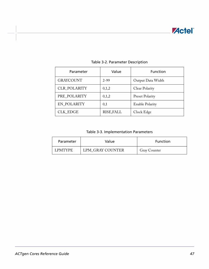
Table 3-2. Parameter Description
Parameter Value Function
GRAYCOUNT 2-99 Output Data Width
CLR_POLARITY 0,1,2 Clear Polarity
PRE_POLARITY 0,1,2 Preset Polarity
EN_POLARITY 0,1 Enable Polarity
CLK_EDGE RISE,FALL Clock Edge
Table 3-3. Implementation Parameters
Parameter Value Function
LPMTYPE LPM_GRAY COUNTER Gray Counter
ACTgen Cores Reference Guide 47

Binary to Gray / Gray to Binary
Features• Parameterized for Data Width
Family support54SX, Axcelerator
DescriptionACTgen can generate Binary to Gray and Gray to Binary Converters parameterized for a specified Data Width.
Datain Dataout
Table 3-4. Port Description
Port Name Size Type Req/Opt Function
Datain WIDTH Input Req. Input Data
Dataout WIDTH Output Req. Output Data
Table 3-5. Parameter Description
Parameter Value Function
GRAYDECODE/WIDTH 2-99 Input/Output Data Width
ACTgen Cores Reference Guide 48

Table 3-6. Implementation Parameters
Parameter Value Function
LPMTYPE LPM_GRAYENCODE/ LPMGRAYDECODEBinary to Gray and Gray to
Binary Converter
ACTgen Cores Reference Guide 49

Converters
50 ACTgen Cores Reference Guide
4Counters
ACTgen Cores Reference Guide 51
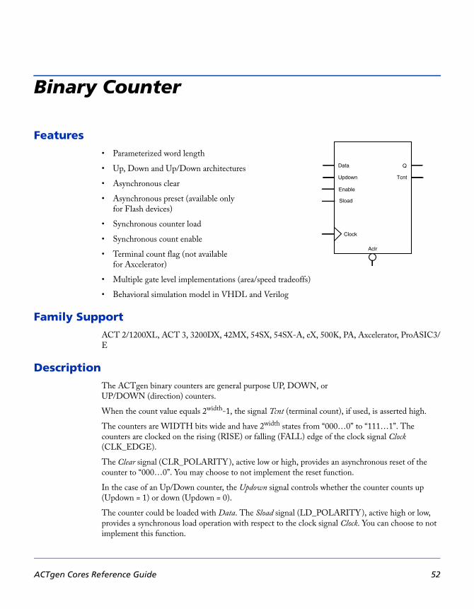
Binary Counter
Features• Parameterized word length
• Up, Down and Up/Down architectures
• Asynchronous clear
• Asynchronous preset (available onlyfor Flash devices)
• Synchronous counter load
• Synchronous count enable
• Terminal count flag (not availablefor Axcelerator)
• Multiple gate level implementations (area/speed tradeoffs)
• Behavioral simulation model in VHDL and Verilog
Family SupportACT 2/1200XL, ACT 3, 3200DX, 42MX, 54SX, 54SX-A, eX, 500K, PA, Axcelerator, ProASIC3/E
DescriptionThe ACTgen binary counters are general purpose UP, DOWN, or UP/DOWN (direction) counters.
When the count value equals 2width-1, the signal Tcnt (terminal count), if used, is asserted high.
The counters are WIDTH bits wide and have 2width states from “000…0” to “111…1”. The counters are clocked on the rising (RISE) or falling (FALL) edge of the clock signal Clock (CLK_EDGE).
The Clear signal (CLR_POLARITY), active low or high, provides an asynchronous reset of the counter to “000…0”. You may choose to not implement the reset function.
In the case of an Up/Down counter, the Updown signal controls whether the counter counts up (Updown = 1) or down (Updown = 0).
The counter could be loaded with Data. The Sload signal (LD_POLARITY), active high or low, provides a synchronous load operation with respect to the clock signal Clock. You can choose to not implement this function.
Data
Updown
Enable
Clock
Q
Tcnt
Aclr
Sload
ACTgen Cores Reference Guide 52

The ACTgen counters have a count enable signal Enable (EN_POLARITY). Enable can be active high or low. When Enable is not active, the counter is disabled and the internal state is unchanged.
Table 4-1. Port Description
Port Name
Size TypeReq./Opt.
Function
Data WIDTH input Opt. Counter load input
Aclr 1 input Opt. Asynchronous counter reset
Enable 1 input Req. Counter enable
Sload 1 input Opt. Synchronous counter load
Clock 1 input Req. Clock
Updown 1 input Opt.UP (Updown = 1), DOWN (Updown = 0)
Q WIDTH output Req. Counter output bus
Tcnt 1 output Opt. Terminal count (active high)
Table 4-2. Parameter Description
Parameter Value Function
WIDTH 2-32 Word length of Data and Q
DIRECTION UP DOWN UPDOWN Counter direction
CLR_POLARITY 0 1 2Aclr can be active low, active high or not used
EN_POLARITY 0 1Enable can be active low, active high
LD_POLARITY 0 1 2Sload can be active low, active high or not used
CLK_EDGE RISE FALL
ACTgen Cores Reference Guide 53

Counters
TCNT_POLARITY 1 2Tcnt can be active high or not used
Table 4-3. Fan-in Control Parameters
Parameter Value
CLR_FANIN AUTO MANUAL
CLR_VAL <val> [default value for AUTO is 8, 1 for MANUAL]
LD_FANIN AUTO MANUAL
LD_VAL <val> [default value for AUTO is 6, 1 for MANUAL]
CLK_FANIN AUTO MANUAL
CLK_VAL <val> [default value for AUTO is 8, 1 for MANUAL]
Table 4-4. Implementation Parameters
Parameter Value Description Family
LPMTYPELPM_COUNTER
Counter category
LPM_HINT LLCNT Prescaled model All
TLACNT Register look ahead model All
FBCNT Fast Balanced model 54SX, 54SX-A
BCNT Balanced model All
LECNT Fast Enable Balanced All
COMPCNT Compact model All
RIPPLE Ripple model All
Table 4-2. Parameter Description (Continued)
Parameter Value Function
54 ACTgen Cores Reference Guide

ImplementationsThis section decribes the implementation of the Pre-Scaled Counter, Register Look Ahead Counter, Fast Balanced Counter and the Balanced Counter.
Pre-Scaled Counter
The pre-scaled counter achieves absolute maximum count and count enable performance by sacrificing synchronous load performance. This counter registers the two least significant bits and uses them as an enable for the upper bits. Count performance is limited only by the delay in the lower two bits and the enable path for the upper bits. Because the upper bits are only updated (enabled) every fourth cycle, they can accommodate more delay (up to one-fourth the clock frequency).
There are two limitations related to the use of the pre-scaled counter. The first is in analyzing the actual performance of the counter. The second is correctly performing data load functions; these two limitations are related. Two parameters must be measured to overcome these two limitations. The first parameter that must be measured is the worst internal delay inside the counter. The second parameter is the worst delay from Q0/Q1 to any upper bit. The minimum count period is then defined by the greater value of these two parameters.
The load function is a slave of the maximum internal path delay in the pre-scaled counter. The load function must be held for as many clock periods as required to exceed the maximum internal delay;
Table 4-5. Functional Descriptiona
a. Assume Aclr is active low, Enable is active high, Sload is active high, Clock is rising, Tcnt isactive high
Data Aclr Enable Sload ClockUp
downQn+1 Tcnt n+1
X 0 X X X X 0’s 0
X 1 X X ¦ X Qn Qn+1== 2width-1
X 1 0 0 ¦ X Qn Qn+1== 2width-1
m 1 X 1 ¦ X m Qn+1== 2width-1
X 1 1 0 ¦ 1 Qn + 1 Qn+1== 2width-1
X 1 1 0 ¦ 0 Qn - 1 Qn+1== 2width-1
ACTgen Cores Reference Guide 55

Counters
this ensures that all internal nodes are settled and that correct count operation can be performed. This requirement can be waived if you can guarantee that 0’s will always be loaded in Q0 and Q1 (resulting in only a single load cycle).
The count path in pre-scaled counters without Sload or Enable functions only have a single logic level for ACT 2/1200XL, ACT 3, 3200DX, 42MX 54SX, 54SX-A, and eX. All other combinations of pre-scaled counters have two logic levels in their count path. In these cases, given the two limitations mentioned previously related to the pre-scaled counter, use the Register Look Ahead or Fast Balanced counters.
Register Look Ahead Counter
This counter achieves the absolute maximum performance for the count, count enable, and synchronous load functions. The counter operates by registering intermediate count values providing “look-ahead” carry circuitry. As a result, this counter variation requires more flip-flops (sequential modules) than other counters.
Fast Balanced Counter
This counter is only available for the 54SX, 54SX-A, and eX families. It takes advantage of the architectural features of these families, including flip-flops with built-in enable and more powerful combinatorial cells. Using these two features, it is possible to build a very fast and compact binary counter without using “look-ahead” carry circuitry. This counter should be preferred over all the others available for this family.
Balanced Counter
This counter achieves high performance for both the count and enable functions using standard design approaches. Module count performance is sacrificed to maintain high speed. This counter is the result of the performance balance between the count/enable functions and the balance between the performance/cost in building this architecture. This counter should address most counter needs for the ACT 1, ACT 2/1200XL, ACT 3, 3200DX, 40MX and 42MX families.
Fast Enable Counter
This compact counter is fully synchronous and has higher performance than the ripple counter. However, this counter should only be used in moderate performance applications, especially for large widths.
Ripple Counter
The ripple counter is an asynchronous counter where the Q of each bit feeds the clock of the next bit; performance is sacrificed to build this variation. However, the ripple counter uses the least amount of logic resources. This counter should only be used in very low-performance applications or for very small counters.
56 ACTgen Cores Reference Guide

Because of the asynchronous nature of the count function, this counter does not have a synchronous load function.
Pseudo Random Counter
A Pseudo Random Counter is available in ACTgen using an LFSR architecture. The Linear Feedback Shift Register offers an efficient architecture for building very fast Pseudo Random Counters.
Figure 4-1. Pseudo Random Counter Generic Architecture
The Pseudo Random core architecture core is a simple shift register chain that uses two taps (one logic level) for the following widths: 2-7, 9-11, 15, 17, 18, 20-23, 25, 28, 29, and 31. The ACTgen PRNG core uses five taps (three logic levels) for the following widths: 8, 12-14, 16, 19, 24, 26, 27, 30, and 32. The five-tap architecture operates slower than the two-tap implementation.
Modulo Counter
As counter size increases, the amount and complexity of support logic also increases. LFSR base counters achieve high performance using very few logic resources. The Modulo Counter is designed to provide two logic levels independently of the chosen modulo value. The architecture borrows some look-ahead techniques previously used in the register look-ahead counter.
The example below is based on a modulo-6 counter with the following characteristics:
• Active-HIGH clock edge
• Active-LOW asynchronous clear
• Active-HIGH synchronous clear
1 2 3 4
A
B
Y
N M
ICA
ACTgen Cores Reference Guide 57

Counters
• No Enable
Figure 4-2. Modulo Counter Sample
Q
Module = 6
X
X
0 1 3 6 5 2 0 1 3
Clock
Aclr
Tent
58 ACTgen Cores Reference Guide

5Decoder
ACTgen Cores Reference Guide 59

Decoder
Features• Parameterized output size (DECODES)
• Behavioral simulation model in VHDL and Verilog
Family SupportACT 1, ACT 2/1200XL, ACT 3, 3200DX, 40 MX, 42MX, 54SX, 54SX-A, eX, 500K, PA, Axcelerator, ProASIC3/E
Description
Enable
EqData
Table 5-1. Port Description
Port Name Size Type Req/Opt Function
Data declna
a. decln is an integer and log2 (DECODES) = decln d<log2 (DECODES + 1. If decln is equalto 1, then Data is scalar, else Data is a bus.
input Req. Input data
Enable 1 input Opt. Enable
Eq DECODES output Req. output
Table 5-2. Parameter Description
Parameter Value Function
DECODES 2-32 Word length of Eq
EN_POLARITY 0 1 2 Enable polarity (active high, active low or not used)
ACTgen Cores Reference Guide 60

EQ_POLARITY 0 1 Eq polarity (active low or active high)
Table 5-3. Functional Descriptiona
a. Assume enable is active low and Eq is active high.
Data Enable Eq
X 0 0’s
m 1decb (m)==decodes-1 &&c dec(m)==decodes-2 && … && dec(m)==0
b. dec(m) defines the decimal value of m
c. && indicates bity concatenation
Table 5-2. Parameter Description
Parameter Value Function
ACTgen Cores Reference Guide 61

Decoder
62 ACTgen Cores Reference Guide

6I/Os
ACTgen Cores Reference Guide 63

Input Buffers
Features• Parameterized for data width
• Choice of data buffers (Regular, Special, Pull-Up, Pull-Down)
Family supportACT2/1200XL, ACT3, 3200DX, 42MX, 54SX, 54SX-A, eX, 500K, PA, Axcelerator, ProASIC3/E
DescriptionACTgen generates different types of Input Buffers with specified data width.
Table 6-1. Port Description
Port Name Size Type Req/Opt Function
PAD WIDTH Input Req. Input Data
PADP (LVDS and LVPECL,
Axcelerator Only)WIDTH Input Req.
Input Data for LVDS and
LVPECL
PADN(LVDS and LVPECL,
Axcelerator Only)WIDTH Input Req.
Input Data for LVDS and
LVPECL
Y WIDTH Output Req. Output Data
Table 6-2. Parameter Description
Parameter Value Function
WIDTH 1-99 (Limit may vary depending on the family) Data Width
PULLUP (Flash Only) NO / YES Choice of Pull-up version
ACTgen Cores Reference Guide 64

VOLT (Flash Only) 0,1,2
Choice of different voltage
levels. 3.3v, 2.5v or
2.5v(Low Power)
TYPE
(Axcelerator Only)
REG, LVCMOS25, LVCMOS18, LVCMOS15, PCI, PCIX, GTLP25,
GTLP33, HSTL_I, HSTL_II, SSTL3_I,
SSTL3_II, SSTL2_I, SSTL2_II, LVDS,
LVPECL, LVCMOS25U, LVCMOS25D, LVCMOS18U, LVCMOS18D,
LVCMOS15U, LVCMOS15D.
Type of Buffer
Table 6-3. Implementation Parameters
Parameter Value Description
LPMTYPE LPM_IO/ LPM_IB_IO (Flash) Input Buffers
LPM_HINT
INBUF / IB (Flash) Regular Input Buffers
INBUF_SP (Axcelerator Only) Special Input Buffers
INBUF_PU (Axcelerator Only) Pull-up Input Buffers
INBUF_PD (Axcelerator Only) Pull-down Input Buffers
Table 6-2. Parameter Description (Continued)
Parameter Value Function
ACTgen Cores Reference Guide 65

Output Buffers
Features• Parameterized for data width
• Choice of buffers (Regular, Special)
Family supportACT2/1200XL, ACT3, 3200DX, 42MX, 54SX, 54SX-A, eX, 500K, PA, Axcelerator, ProASIC3/E
DescriptionACTgen generates different types of Output Buffers with specified data width.
Table 6-4. Port Description
Port Name Size Type Req/Opt Function
Data/A (Flash) WIDTH Input Req. Input Data
PAD WIDTH Output Req. Output Data
Table 6-5. Parameter Description
Parameter Value Function
WIDTH1-99 (Limit may vary depending on the
family)Data Width
VOLT (Flash Only) 0,1,2,3,4,5
Choice of different voltage levels.
3.3v(PCI), 3.3v & Low Strength, 2.5v & High Strength, 2.5v & Low
Strength, 2.5v(Low Power) & High
Strength, or 2.5v(Low Power) & Low Strength
ACTgen Cores Reference Guide 66

SLEW 0,1,2Choice of different slew rates. Low,
Normal or High
TYPE
(Axcelerator Only)
REG, S_8, S_12, S_16, S_24, F_8, F_12,
F_16, F_24, LVCMOS25, LVCMOS18, LVCMOS15, PCI, PCIX, GTLP25,
GTLP33, HSTL_I, HSTL_II, SSTL3_I,
SSTL3_II, SSTL2_I, SSTL2_II, LVDS,
LVPECL.
Type of Buffer Note: "S" in S_*
denotes Low Slew Rate and "F" in
F_* denotes High Slew Rate. Also 8,12,16,24 denote Output drive
strengths of 1x, 2x, 3x, 4x respectively
Table 6-6. Implementation Parameters
Parameter Value Description
LPMTYPE LPM_IO / LPM_OB_IO (Flash) Output Buffers
LPM_HINTOUTBUF / OB (Flash) Regular Output Buffers
OUTBUF_SP (Axcelerator Only) Special Output Buffers
Table 6-5. Parameter Description (Continued)
Parameter Value Function
ACTgen Cores Reference Guide 67

Bi-Directional Buffers
Features• Parameterized for data width
• Choice of buffers (Regular, Special, Pull-up, Pull-down)
Family supportACT2/1200XL, ACT3, 3200DX, 42MX, 54SX, 54SX-A, eX, 500K, PA, Axcelerator, ProASIC3/E
DescriptionACTgen generates different types of Input Buffers with specified data width.
Table 6-7. Port Description
Port Name Size TypeReq/Opt
Function
PAD WIDTH Inout Req. Inout Data
Data / A (Flash) WIDTH Input Req. Input Data
Trien / ENABLE (Flash)
1 Input Req. Enable
Y WIDTHOutput
Req.Output Data
ACTgen Cores Reference Guide 68

Table 6-8. Parameter Description
Parameter Value Function
WIDTH1-99 (Limit may vary depending on
the family)Data Width
VOLT (Flash Only) 0,1,2,3,4,5
Choice of different voltage levels.
3.3v(PCI), 3.3v & Low Strength, 2.5v & High Strength, 2.5v & Low
Strength, 2.5v(Low Power) & High
Strength, or 2.5v(Low Power) &
Low Strength
SLEW (Flash Only) 0,1,2Choice of the slew rates: Low, Normal, or High
PULLUP NO / YES Choice of Pull up version
TRIEN_POLARITY /
EN_POLARITY
(Flash)
0,1 Enable Polarity
TYPE (Axcelerator Only)
REG, S_8, S_12, S_16, S_24, F_8, F_12, F_16, F_24, LVCMOS25,
LVCMOS18, LVCMOS15, PCI,
PCIX, GTLP25, GTLP33, S_8U, S_12U, S_16U, S_24U, F_8U,
F_12U, F_16U, F_24U, S_8D,
S_12D, S_16D, S_24D, F_8D, F_12D, F_16D, F_24D,
LVCMOS25U, LVCMOS25D,
LVCMOS18U, LVCMOS18D, LVCMOS15U, LVCMOS15D,
HSTL_I, SSTL2_I, SSTL2_II,
SSTL3_I, SSTL3_II
Type of Buffer. Note : "S" in S_*
denotes Low Slew Rage and "F" in F_* denotes High Slew Rate. Also
8,12,16,24 denote Output drive
strengths of 1x, 2x, 3x, 4x respectively
ACTgen Cores Reference Guide 69

I/Os
Table 6-9. Implementation Parameters
Parameter Value Function
LPMTYPE LPM_IO / LPM_IOB_IO Bi-directional Buffers
LPM_HINT
BIBUF / IOB, GLMIOB (Flash)
Regular Bi-directional Buffers / IO pad with Global Connection, Two Multiplexed Pads & Global Connection (Flash)
BIBUF_SP (Axcelerator Only) Special Bi-directional Buffers
BIBUF_PU (Axcelerator Only) Pull-up Bi-directional Buffers
BIBUF_PD (Axcelerator Only) Pull-down Bi-directional Buffers
70 ACTgen Cores Reference Guide

Tri-State Buffers
Features• Parameterized for data width
• Choice of buffers (Regular, Special, Pull-up, Pull-down)
Family supportACT2/1200XL, ACT3, 3200DX, 42MX, 54SX, 54SX-A, eX, 500K, PA, Axcelerator, ProASIC3/E
DescriptionACTgen generates different types of Input Buffers with specified data width.
Table 6-10. Port Description
Port Name Size TypeReq/Opt
Function
PAD WIDTH Inout Req. Inout Data
Data / A (Flash) WIDTH Input Req. Input Data
Trien / ENABLE (Flash)
1 Input Req. Enable
Table 6-11. Parameter Description
Parameter Value Function
WIDTH 1-99 (Limit may vary depending on the family) Data Width
ACTgen Cores Reference Guide 71

I/Os
VOLT (Flash Only) 0,1,2,3,4,5
Choice of different voltage levels. 3.3v (PCI),
3.3v & Low Strength, 2.5v & High Strength, 2.5v & Low Strength, 2.5v (Low Power) & High
Strength, or 2.5v (Low Power) & Low Strength
SLEW (Flash Only) 0,1,2 Choice of the slew rates: Low, Normal, or High
TRIEN_POLARITY /
EN_POLARITY
(Flash)
0,1 Enable Polarity
TYPE (Axcelerator
Only)
REG, S_8, S_12, S_16, S_24, F_8, F_12, F_16, F_24, LVCMOS25, LVCMOS18,
LVCMOS15, PCI, PCIX, GTLP25,
GTLP33, S_8U, S_12U, S_16U, S_24U, F_8U, F_12U, F_16U, F_24U, S_8D, S_12D,
S_16D, S_24D, F_8D, F_12D, F_16D,
F_24D, LVCMOS25U, LVCMOS25D, LVCMOS18U, LVCMOS18D,
LVCMOS15U, LVCMOS15D, HSTL_I,
SSTL2_I, SSTL2_II, SSTL3_I, SSTL3_II
Type of Buffer. Note : "S" in S_* denotes Low Slew Rage and "F" in F_* denotes High Slew
Rate. Also 8,12,16,24 denote Output drive
strengths of 1x, 2x, 3x, 4x respectively
Table 6-11. Parameter Description (Continued)
Parameter Value Function
Table 6-12. Implementation Parameters
Parameter Value Function
LPMTYPE LPM_IO / LPM_OB_IO Tri-State buffers
LPM_HINT
TRIBUFF / OTB (Flash) Regular Tri-State Buffers
TRIBUFF_SP (Axcelerator Only) Special Tri-State Buffers
TRIBUFF_PU (Axcelerator Only) Pull-up Tri-State Buffers
TRIBUFF_PD (Axcelerator Only) Pull-down Tri-State Buffers
72 ACTgen Cores Reference Guide

Global Buffers
Features• Parameterized for data width
• Choice of buffers (Regular, Multiplexed, Internal Driver)
Family support500K, PA, ProASIC3/E
DescriptionACTgen generates different types of Input Buffers with specified data width.
Table 6-13. Port Description
Port Name Size Type Req/Opt Function
PAD WIDTH Input Req. Inout Data
A WIDTH Input Req. Input Data
ENABLE 1 Input Req. Enable
GL 1 Output Req. Output Data
Y WIDTH Output Req. Output Data
Table 6-14. Parameter Description
Parameter Value Function
WIDTH1-499 (Limit may vary depending on the type)
Data Width
ACTgen Cores Reference Guide 73

I/Os
VOLT 0,1,2Choice of different voltage levels: 3.3V, 2.5V, 2.5V (Low Power)
PULLUP NO / YES Choice of Pull-up version
Table 6-15. Implementation Parameters
Parameter Value Function
LPMTYPE LPM_GL_IO All buffers
LPM_HINT
GL Standard Global buffer
GLIB Standard Global buffer w/ an Input bufer
GLMIBStandard Global buffer with Multiplexed Input buffer
GLINT Global internal driver
Table 6-14. Parameter Description (Continued)
Parameter Value Function
74 ACTgen Cores Reference Guide

PECL Global Buffers
Features• Parameterized for data width
• Choice of buffers (Direct to Global, Multiplexed with Internal Signal)
Family supportPA
DescriptionACTgen generates different types of Input Buffers with specified data width.
Table 6-16. Port Description
Port Name Size Type Req/Opt Function
PECLIN WIDTH Input Req. Input Data
PECLREF WIDTH Input Req. Reference Data
A WIDTH Input Req. Input Data
ENABLE 1 Input Req. Enable
GL WIDTH Output Req. Output Data
Y WIDTH Output Req. Output Data
Table 6-17. Parameter Description
Parameter Value Function
WIDTH 1-2 Data Width
ACTgen Cores Reference Guide 75

I/Os
Table 6-18. Implementation Parameters
Parameter Value Function
LPMTYPE LPM_GLPE_IO PECL Global buffers
LPM_HINTGLPE Direct to Global
GLPEMIB Multiplexed with Internal Signal
76 ACTgen Cores Reference Guide

Dual Data Rate Register
Features• Parameterized for Data Width
and almost Full/Empty Values
• Choice of Input buffers for Axcelerator
• Choice of Input, Output, and Bi-directional buffers for ProASIC3/E
Family supportAxcelerator, ProASIC3/E
DescriptionACTgen can generate Dual Data Rate Registers parameterized for a specific Data Width and with a choice of the type of Input Buffers for Axcelerator and ProASIC3/E.
PAD PRE
E
QR
QF
CLK
CLR
Table 6-19. Port Description - Input Buffer plus DDR Register
Port Name Size Type Req/Opt Function
PAD WIDTH Input Req. Input Data
QR WIDTH Output Req. Output Data
QF WIDTH Output Req. Output Data
E 1 Input Req. Enable
CLK 1 Input Req. Clock
CLR 1 Input Req. Clear
PRE 1 Output Req. Preset
ACTgen Cores Reference Guide 77

I/Os
Table 6-20. Port Description - Bidirectional Buffer plus DDR Register
Port Name Size Type Req/Opt Function
PAD WIDTH Input/Output Req. Input/Output Data
DataR WIDTH Input/Output Req. Input/Output Data
DataF WIDTH Input/Output Req. Input/Output Data
TriEN 1 Input Req. Enable
CLK 1 Input Req. Clock
CLR 1 Input Req. Clear
Table 6-21. Port Description - DDR Register plus Output Buffer
Port Name Size Type Req/Opt Function
PAD WIDTH Input Req. Output Data
DataR WIDTH Output Req. Input Data
DataF WIDTH Output Req. Input Data
E 1 Input Req. Enable
CLK 1 Input Req. Clock
CLR 1 Input Req. Clear
PRE 1 Output Req. Preset
78 ACTgen Cores Reference Guide

Table 6-22. Parameter Description
Parameter Value Function
WIDTH 1-128 Data Width
ACTgen Cores Reference Guide 79

I/Os
80 ACTgen Cores Reference Guide

7Logic
ACTgen Cores Reference Guide 81

Logic (AND)
Features• Parameterized AND size
• Behavioral simulation model in VHDL and Verilog
Family SupportACT 1, ACT 2/1200XL, ACT 3, 3200DX, 40MX, 42MX, 54SX, 54SX-A, eX, 500K, PA, Axcelerator, , ProASIC3/E
Description
Data Result
Table 7-1. Port Description
Port Name Size Type Req/Opt Function
Data SIZE input Req. Input data
Result 1 output Req. output
Table 7-2. Parameter Description
Parameter Value Function
SIZE 2-64 Word length of data
RESULT_POLARITY 0 1 Output polarity (active low or active high)
Table 7-3. Functional Descriptiona
a. result is active; highresult is active high
Data Result
m m[0] and m[1] and … and m[SIZE-1]
ACTgen Cores Reference Guide 82

Logic (OR)
Features• Parameterized OR size
• Behavioral simulation model in VHDL and Verilog
Family SupportACT 1, ACT 2/1200XL, ACT 3, 3200DX, 40MX, 42MX, 54SX, 54SX-A, eX, 500K, PA, Axcelerator, , ProASIC3/E
Description
Data Result
Table 7-4. Port Description
Port Name Size Type Req/Opt Function
Data SIZE input Req. input data
Result 1 output Req. output
Table 7-5. Parameter Description
Parameter Value Function
SIZE 2-64 Word length of data
RESULT_POLARITY 0 1 Output polarity (active low or active high)
Table 7-6. Functional Descriptiona
a. result is active high
Data Result
m m[0] or m[1] or … or m[SIZE-1]
ACTgen Cores Reference Guide 83

Logic (XOR)
Features• Parameterized XOR size
• Behavioral simulation model in VHDL and Verilog
Family SupportACT 1, ACT 2/1200XL, ACT 3, 3200DX, 40MX, 42MX, 54SX, 54SX-A, eX, 500K, PA, Axcelerator, , ProASIC3/E
Description
Data Result
Table 7-7. Port Description
Port Name Size Type Req/Opt Function
Data SIZE input Req. input data
Result 1 output Req. output
Table 7-8. Parameter Description
Parameter Value Function
SIZE 2-64 Word length of data
RESULT_POLARITY 0 1 Output polarity (active low or active high)
Table 7-9. Functional Descriptiona
a. result is active high
Data Result
m m[0] xor m[1] xor … xor m[SIZE-1]
ACTgen Cores Reference Guide 84

8Multiplexer
ACTgen Cores Reference Guide 85

Multiplexer
Features• Parameterized word length
• Parameterized multiplexer input number
• Behavioral simulation model in VHDL and Verilog
Family SupportACT 1, ACT 2/1200XL, ACT 3, 3200DX, 40MX, 42MX, 54SX, 54SX-A, eX, 500K, PA, Axcelerator, , ProASIC3/E
Description
Data Result
SEL
Table 8-1. Port Description
Port Name Size Type Req/Opt Function
Data0_port WIDTH Input Req. Input data
Data1_port WIDTH Input Req. Input data
… … … … …
DataSIZE-1_port WIDTH Input Req. Input data
Sel0 1 Input Req. Select line
Sel1 1 Input Req. Select line
… … … … …
SelSIZELN-1 1 Input Req. Select line
Result WIDTH Output Req. output
ACTgen Cores Reference Guide 86

Table 8-2. Parameter Description
Parameter Family Value Function
WIDTHAPA, 500K 1-48
Word length of DataAll Others 1-32
SIZE All 2-32 Number of data inputs
Table 8-3. Functional Description
Data0
Data1 … DataSIZE-1 Sel0 Sel1 … SelSIZELN-1 Result
m0 m1 … mSIZE-1 0 0 … 0 m0
m0 m1 … mSIZE-1 1 0 … 0 m1
… … … … … … … … …
m0 m1 … mSIZE-1 1 1 … 1 mSIZE-1
ACTgen Cores Reference Guide 87

Multiplexer
88 ACTgen Cores Reference Guide

9Minicores
ACTgen Cores Reference Guide 89

FIR Filter
Features• Variable input data width:
2 to16 bit input data
• Variable output data width: 3 to 64 bit output data
• Support for up to 64 taps
• Support of symmetric coefficients
• Optional IO insertion
• Optional registers for filter in- and output
• Verilog RTL model for simulation
• VHDL RTL model for synthesis1
Family support54SX, 54SX-A, 500K, PA, Axcelerator, , ProASIC3/E
Design FlowAn overview of the design flow required for the FIR filter is shown in Figure 9-1.
Figure 9-1. FIR Filter Design Flow
1. Synthesized filter designs are usually slower, but more compact.
Data Qout
Aclr
Clock
System LevelDesign Tool
ACTgen
Designer
.gen File w/ Implementation
Parameters
FIR.edn
TOP.ednFPGA
ACTgen Cores Reference Guide 90

Generate the filter coefficients and other implementation parameters using a system level design tool (like Matlab). This information is made available for ACTgen in form of a <design>.gen file. .
From that point on it follows the regular design flow as described in the Actel Quick Start Guide.
DescriptionThe ACTgen FIR-filter core supports symmetric, high-speed, parallel FIR-filters with up to 64 time taps.
Figure 9-2. Tap Transposed from FIR Filter
The architecture is a variation of the "transposed form" of the FIR-filter as shown in Figure 9-2, making use of ACTgen's signed Constant Multiplier. The data is assumed to be signed. Data- and coefficient widths are the same (D_WIDTH).
Figure 9-2 suggests that coefficients with a value of 0 are desirable for this type of architecture, since they will not generate any multiplication hardware. "Halfband" filters are trying to maximize the number of 0-coefficients and might result in significant area savings over regular filters of the same order .
Table 9-1. Port Description
Port Name Size Type Req/Opt? Function
Data D_WIDTH input Req. Input Data
Clock 1 input Req. Filter clock
Aclr 1 input Opt. Asynchronous Clear
Qout O_WIDTH input Req. Filter output = Σ χι * δι
* * * * *C0C1C2C3C4
Data
Qout
ACTgen Cores Reference Guide 91

Minicores
The output width O_WIDTH has no impact on the filter size. Internally, ACTgen always uses the maximum precision filter, unless specified otherwise using the internal precision parameter PREC. If you set O_WIDTH to 0, ACTgen usese the maximum output resolution (MAX_RES). For values of O_WIDTH greater than MAX_RES the result is sign-extended. For values of O_WIDTH smaller than MAX_RES ACTgen cuts some of the lower bits. An upper estimate for MAX_RES is
For example a 12-tap filter with 8-bit data and coefficients might yield up to (8 + 8 + 4 ) bit = 20 bit output resolution.
The coefficients C1 to C16 are positive integers, which will be interpreted as two's complement numbers. That means 0 to 2C_WIDTH-1-1 are considered positive, and 2C_WIDTH-1-1 to 2C_WIDTH-1 will be interpreted as negative numbers.
Only unique coefficients need to be specified properly, all other coefficients need to be set to any value, e.g. "0". An N-tap filter requires (N / 2) + (N % 2) unique coefficients.
Table 9-2. Parameter Description
Parameter Value Function
D_WIDTH 3 .. 16 Input Data Width
O_WIDTH 3 .. 64 Output Data Width
TAPS 3 .. 64 Number of time taps
CLK_EDGE RISE FALL Clock sensitivity
CLR_POLA 2 0 1 None, active high, active low
PREC Internal precision
INSERT_PAD NO YES Pad insertion
INSERT_IOREG NO YES Register inputs and outputs
C1 … C32 0 .. 2C_WIDTH 2's complement coefficients (integers)
MAX_RES 2 D_WIDTH 2 TAPS( )log+×≤
92 ACTgen Cores Reference Guide

Only unique coefficients need to be specified properly, all other coefficients need to be set to any value, e.g. "0". An N-tap filter requires (N / 2) + (N % 2) unique coefficients.
Internal Precision (PREC) specifies the minimum number of bits
• For the time tab registers
• From multiplier outputs kept for further processing
• From adder outputs kept for further processing
Table 9-3. Parameter Rules
Family Variation Parameter rules
All FIR2 PREC >= O_WIDTH
54SX, 54SX-A All O_WIDTH <= 32
54SX, 54SX-A All TAPS <= 32
Table 9-4. Implementation Parameters
Parameter Value Description
LPMTYPE LPM_FIR FIR-filter category
LPM_HINTFIR1 Basic Options
FIR2 Advanced Options
Table 9-5. Internal Precision (PREC)
Variation Value Description
Basic Options 97, 0 Maximum output resolution, same as O_WIDTH
Advanced Options PREC See parameter rules
ACTgen Cores Reference Guide 93

Minicores
Currently the RTL-model does not reflect the PREC parameter, so there may be differences between the simulated output of the structural netlist and the RTL-model for the low-order bits.
Integer Values Coefficient File
The Integer Values Coefficient File consists of the conversion of the quantized coefficients into regular integers. This file can be directly imported into ACTgen.
Table 9-6. Sample Integer Coefficient File
20482037048204818920630102663001892204848020372048
94 ACTgen Cores Reference Guide

CRC Minicore
Features• General-purpose Cyclic Redundancy Code generator
• Fully-synchronous, single-clock operation (greater than 100 MHZ for many configurations)
• Parameterized arbitrary polynomial (from 1 up to 64-bit)
• Parameterized data input width
• Parameterized register initialization
• Parameterized bit and byte ordering
• Parameterized bit pattern for CRC output XOR with
Family supportAxcelerator
DescriptionThe CRC Minicore is a universal Cyclic Redundancy Check (CRC) Polynomial generator that validates data frames and ensures data integrity during data transmission.
To meet different application requirements, the CRC minicore provides many different configuration parameters. These parameters control data width, a register initialization value, and other CRC output data characteristics.
• Data width specifies the number of bits over which the CRC Minicore generates the CRC value in a single clock cycle. For example, a CRC32 with 8-bit data width performs CRC calculations on 8 bits per clock.
• Register initialization provides the seed value for CRC generation.
• Additional parameters provide additional flexibility in controlling CRC data characteristics.
For example, the CRC output XOR bit pattern parameter (XOROUT) controls inversion of the CRC value before injecting it into the data stream. Although the CRC Minicore generator provides seven commonly-used CRC polynomials, ACTgen also allows entry of an arbitrary polynomial. The polynomial bit size spans 1 to 64 inclusive.
ACTgen Cores Reference Guide 95

Minicores
Table 9-7. XOROUT Configuration
XOROUT Description
1 All bits are not inverted (000000000) xor CRC
2 All bits are inverted (..FFFFFFFF) xor CRC
3 Even bits are inverted, odd bits are not inverted (….10101010) xor CRC
4 Odd bits are inverted, even bits are not inverted (….01010101) xor CRC
Table 9-8. Port Description
Port Name width Description
CLK 1 Clock port
rst_n 1 Asynchronous reset
init_n 1 Synchronous load CRC value
enable 1 CRC enable/disable control
data_in Data_width Input data word
CRC_in Poly_size CRC value to be load in
CRC_out Poly_size Generated CRC value
96 ACTgen Cores Reference Guide

Table 9-9. CRC Operation Control
rst_n init_n enable shift_run Description
0 x x x Asynchronous reset, set to initial register value
1 0 x x Synchronous initialization
1 1 0 xDisable CRC generation, register holds the current value
1 1 1 0 Generate CRC on the input data
1 1 1 1Normal CRC operation, generate CRC from input data
Table 9-10. Standard CRC Generator Parameters - Description
Name Poly_width Poly_value (HEX) initial xorout
CRC32 32 04C11DB7 FFFF.. FFFFFF....
CRC16/ARC 16 1005 FFFF... FFFFF....
CCIT CRC16 16 1021 FFFF…. FFFFFF….
CANBUS 16 4599 FFFFF... FFFFF....
ATM CRC10 10 233 FFFFF... FFFFF....
ATM CRC8 8 7 FFFF…. FFFFF..….
kermit 16 8408 000000… 000000000
ACTgen Cores Reference Guide 97

Minicores
98 ACTgen Cores Reference Guide

10PLLs
ACTgen Cores Reference Guide 99

PLL for ProASICPLUS
You can use ACTgen to configure PLLs according to your needs, and generate a netlist that has a PLL primitive instantiated with the correct specified configuration
Features• Clock Delay Adjustment
• Clock Frequency Synthesis
• Clock Phase Shifting
Family SupportPA
Parameter Description
Table 10-1. Parameter Description
Parameter Value Function
CLKS 1 2 Primary or Both outputs
FIN 1.5 - 240 MHz Input Frequency
PRIMFREQ 1.5 - 240 MHz Primary Output Frequency
PDELAYVAL 0 - 8 ns Primary Delay value, in steps of .25 ns
PDELAYSIGN 0 1 Positive or Negative primary delay
PPHASESHIFT 0 90 180 270 Primary Phase-shift
PBYPASS 0 1 No Yes. Primary Bypass
FIN2 1.5 - 240 MHzSecondary Input Frequency, Only if PLL is bypassed for Secondary Output
SECFREQ 1.5 - 240 MHz Primary Output Frequency
SDELAYVAL 0 - 8 ns Primary Delay value, in steps of 0.25 nsa
ACTgen Cores Reference Guide 100

Summary of the menu items available when you generate a PLL for ProASICPLUS.
Configuration - Dynamic or Static Configuration
In dynamic mode, designers are able to set all the configuration parameters using either the external JTAG port or an internally-defined serial interface. The dynamic-mode PLL can be switched to static mode during operation by just changing a mode selection bit. This way you can have one stable static configuration, yet for selected sequences of events, you can switch to dynamic mode and run the clock at a different frequency if required. For the Dynamic mode, ACTgen is used to specify a stable default configuration.
Input Clock Frequency - Floating point value between 6.0 and 240 MHz
Primary Clock Frequency - Floating point value between 6.0 and 240 MHz. If the specified frequency cannot be achieved, the closest approximate frequency is provided. There are some restrictions on the possible values of this frequency even in the specified range, based on the PLLCORE limitations. ACTgen takes all these limitations into consideration when generating a PLL. If the specified frequency cannot be achieved, the closest approximate frequency will be provided..
Bypass PLL in Primary Clock - Selecting this checkbox bypasses the PLL for the primary clock. This feature enables you to bypass the PLLCORE functionality and use the surrounding divider and delay elements. When the PLL is bypassed, the primary clock frequency must be equal to or be 1/2, 1/3 or ¼ of input frequency, as only a divider is available in the output path.
SDELAYSIGN 0 1 Positive or Negative primary delay
SPHASESHIFT 0 90 180 270 Primary Phase-shift
SBYPASS 0 1 No Yes. Primary Bypass
FBInternal DeskewedExternal
Feedback
CONF STATIC DYNAMIC Configuration
a. In the GUI, the delay is entered directly as a value between -3.75 and +3.75 without breakingit into sign and value
Table 10-1. Parameter Description (Continued)
Parameter Value Function
ACTgen Cores Reference Guide 101

PLLs
Primary Clock Phase Shift - Supports 4 values 0, 90, 180, 270 degrees. Not valid when PLL is bypassed for primary clock. The secondary clock cannot be phase-shifted.
Selecting a phase shift of 90 degrees and an output divider other than 1 causes ACTgen to return a message about the actual phase shift being 90 divided by the divider.
Primary Clock Delay - This is a floating point between -4.0 and 8.0 with increments of 0.25. When PLL is bypassed for primary clock, only 0, 0.25, 0.5 and 4 ns are valid delays.
Secondary Clock Input Frequency - Floating point value between 1.5 and 240 MHz. This is valid only when secondary clock is selected and PLL is bypassed.
Secondary Clock Output Frequency - Floating point value between 1.5 and 240 MHz. This is valid only when secondary clock is selected. If the specified value cannot be achieved, the closest approximate frequency will be provided.
Bypass PLL in Secondary clock - Selecting this checkbox bypasses the PLL for secondary clock. When the PLL is bypassed, the secondary clock frequency must be equal to or be 1/2, 1/3 or ¼ of secondary input frequency. This feature allows the user to bypass the PLLCORE functionality and use the surrounding divider and delay elements.
Secondary Clock Delay - This is a floating point between -4.0 and 8.0 with increments of 0.25. When PLL is bypassed for secondary clock, only 0, 0.25, 0.5 and 4 ns are the valid delays.
Feedback - A radio button to select between Internal, External and Deskewed feedback.
The clock-conditioning circuitry enables you to implement the feedback clock signal using either the output of the PLL, an internally generated clock, or an external clock. When external feedback is selected, an additional port EXTFB is made available to the user to drive the feedback . The internal feedback signal can be further delayed by a fixed amount designed to emulate the delay through the chip’s clock tree. This allows for clock-line de-skewing operations. This delay is included in the feedback path when deskewed feedback is chosen. This value is dependent on the device you are using.
Table 10-2. Port Description
Name Size Type Req/Opt Function
GLA 1 Output Opt Secondary clock output
GLB 1 Output Req Primary clock output
LOCK 1 Output Req PLL Lock
SDOUT 1 Output Req Output of serial interface shift register
CLK 1 Input Req Input clock for primary clock
102 ACTgen Cores Reference Guide
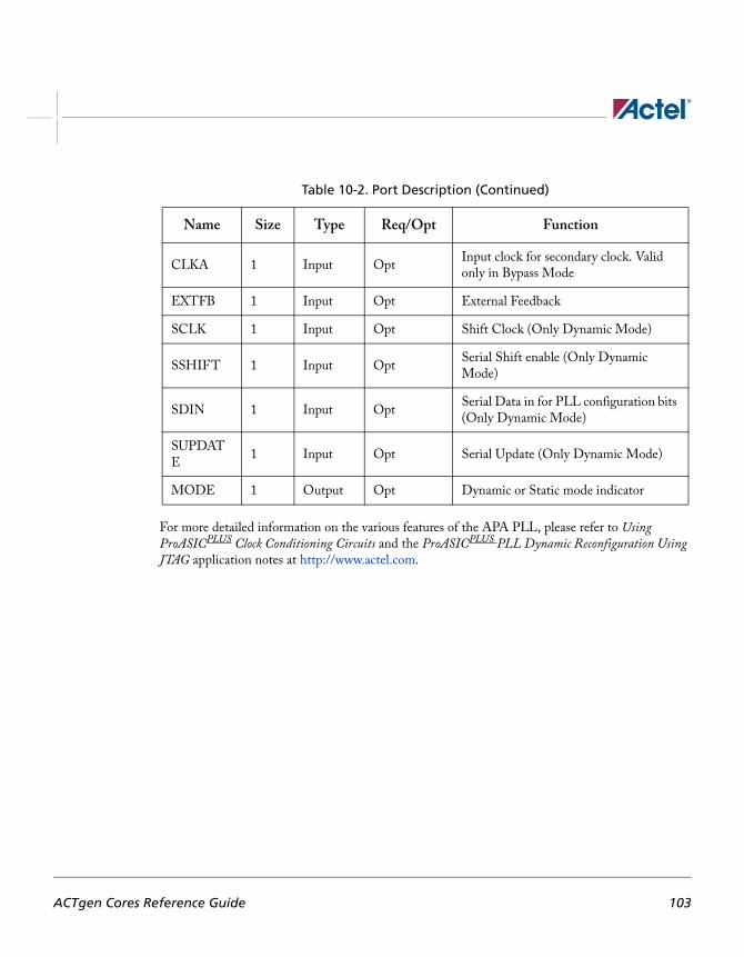
For more detailed information on the various features of the APA PLL, please refer to Using ProASICPLUS Clock Conditioning Circuits and the ProASICPLUS PLL Dynamic Reconfiguration Using
JTAG application notes at http://www.actel.com.
CLKA 1 Input OptInput clock for secondary clock. Valid only in Bypass Mode
EXTFB 1 Input Opt External Feedback
SCLK 1 Input Opt Shift Clock (Only Dynamic Mode)
SSHIFT 1 Input OptSerial Shift enable (Only Dynamic Mode)
SDIN 1 Input OptSerial Data in for PLL configuration bits (Only Dynamic Mode)
SUPDATE
1 Input Opt Serial Update (Only Dynamic Mode)
MODE 1 Output Opt Dynamic or Static mode indicator
Table 10-2. Port Description (Continued)
Name Size Type Req/Opt Function
ACTgen Cores Reference Guide 103

Axcelerator PLL
Features• Clock Delay Minimization
• Clock Frequency Synthesis
• Programmable delay lines for clock delay adjustment
• 6-bit divider in the feedback path for clock multiplication
• 6-bit divider in one of the output paths for clock division
• Cascadable up to 2 PLLs
Family supportAxcelerator
DescriptionThe Axcelerator PLL has two main features. They are:
• Clock Delay Minimization
In this mode the PLL can perform either a positive or negative clock delay operation of up to 3.75ns in increments of 250ps before or after the clock edge of the incoming reference clock. The value of the delay is programmable via the five bits of the DelayLine bus.
• Clock Frequency Synthesis
The multiplier and divider can be used together to synthesize a wide range of output frequencies from the reference clock. Input frequencies are allowed to be in the range of 14 MHz to 200 MHz. Multiplication and division factors are integers in the range of 1 to 64. The maximum allowable output frequency is 1 GHz. The output duty cycle is fixed at 50/50.
Cascading BlocksThe device supports cascading of up to 2 PLLs.
ACTgen Cores Reference Guide 104

Table 10-3. Port Description
Name Size Type Req/Opt Function
RefClk 1 Input Req Reference Clock
PWRDN 1 Input Req Power Down
Lock 1 Output Req PLL Lock
FB 1 Input Opt Feedback (only external feedback)
CLK(freq) 1 Output Opt Clk1 with the required freq
CLK(freq) 1 Output Opt CLK2 with the required freq
Table 10-4. Parameter Description
Parameter Value Function
LPMTYPE LPMPLL PLL category
LPM_HINT
PRIM Only primary output
SEC Only secondary output
BOTH Both outputs
FB Internal External Feedback
IFREQ 14.0 - 200.0 MHz Input Frequency
PFREQ 14.0 - 1000.0 Primary Clock freq
SFREQ 14.0 - 1000.0 Secondary Clock freq
DT STATIC DYNAMIC Delay type
DELAYSIGN +ve -ve Positive or negative delay
DELAYVALUE 0 - 3.75 ns In steps of 250 psa
ACTgen Cores Reference Guide 105

PLLs
Description
The Axcelerator family provides eight PLLs, four on the north side and four on the south side of the device. The outputs of the north-side PLLs can be connected to either hard-wired clock networks or regular nets. The outputs of the south-side PLLs can be connected to either routed clock networks or regular nets. The Axcelerator family PLLs have many outstanding features, including the following:
• PLLs can multiply and/or divide the reference clock frequency by factors ranging from1 to 64. As a result, there are many available output frequencies for each PLL, based on the input frequency. ACTgen automatically calculates the values of the multiplier and divider based on the Input and Output frequencies specified. If the exact value cannot be achieved, ACTgen generates the output frequency that is the closest possible to the required value.
• PLLs are capable of inserting programmable delays on the REFCLK from –3.75ns to +3.75ns with the steps of 250ps. The delay is programmed either statically or dynamically. Dynamic programming means that you can change the delay value during the operation when the device is functional. If you select the dynamic delay, then the 5-bit Delay Line port is added to the generated code and accessible to you.
Refclk is the reference input to the PLL. The frequency of Refclk can vary from 14 MHz to 200 MHz. The reference can be supplied from a dedicated pad or an internal net.
You can select to have an internal or external feedback. Selecting an external feedback adds a port (named FB) to the PLL block, through which the external feedback is passed into the PLL and the internal feedback is blocked.
CASCADE YES NOCascade 2 PLLs to achieve the required output frequency
REFCLKPADDEDICATED EXTERNAL
Source of REFCLK, the Dedicated Pad, or any external net
CLK1OUT HW RC RNClock network to which PLL is connected, Hardwired Clock, Routed Clock, or Routed Net
a. In the GUI, the delay is entered directly as a value between -3.75 and +3.75 without breakingit into sign and value
Table 10-4. Parameter Description
Parameter Value Function
106 ACTgen Cores Reference Guide

Clk(freq) are the output signals from the PLL. The CLK(primary) is defined as refclk * i/j where i is the multiplier and j is the divider. CLK(secondary) is defined as refclk * i
Cascading
Cascading is an option that helps you generate a wider range of output frequencies. If cascading is set to No and the output frequency is chosen as a value that cannot be achieved by fREF * i/j, then the PLL will try to set i and j in order to reach to the closest vicinity of the desired frequency. If cascading is set to Yes, then for the conditions in which the desired frequency is unattainable by a single PLL, another PLL will be cascaded to the first PLL and then the final output frequency is:
In cascading PLLs, the input frequency of each PLL should remain in the range of 14 MHz to 200 MHz.
You must specify the desired output frequencies and the networks that the outputs should drive for the PLL outputs CLK1 and CLK2. Note that if cascading is disabled, the CLK2 frequency can only be a multiple of the reference frequency. As mentioned earlier, if the selected values for output frequencies cannot be achieved, they will be set to the closest possible frequency.
For each output, there are three routing resources. Hard-wired is the HCLK network which reaches to the clock input of R-cells. Selecting a hard-wired output for the PLL implies that the PLL should be located at the north side of the device. If one of the outputs is connected to hard-wired global network, the routed clock network cannot be chosen as the second output because the routed clock network is only accessible by the PLLs on the south side. ACTgen helps you select the output type by keeping the possible outputs active and disabling the illegal combinations (Figure 10-1).
Figure 10-1. Basic PLL Architecture in Axcelerator Devices
For more detailed information on the various features of the Axcelerator PLL, please refer to the Axcelerator Family PLL and Clock Management application note at http://www.actel.com.
fout fREFi1j1-----⎝ ⎠
⎛ ⎞ i2j2-----⎝ ⎠
⎛ ⎞××=
Delay Line
PLL
Delay Line
RefCLK
FB
/i
6
/j
6
CLK1
PowerDown
Lock
CLK2
/i DelayMatch
/i DelayMatch
FBMuxSel
5
DividerIDelayLine
DividerJ
LowFreq
3
Osc
155 MHz
0
1
ACTgen Cores Reference Guide 107

Clock Conditioning / PLL cores for ProASIC3/E
The ProASIC3E Clock Conditioning Circuit (CCC) contains a PLL core, delay lines, clock multipliers/dividers, PLL reset generator (you have no control over the reset), global pads, and all circuitry for the selection and interconnection of the “global” pads to the global network. The PLL Core consists of a Phase Detector, L.P. Filter and a 4-Phase VCO.
The clock conditioning circuit performs the following basic functions:
• Clock phase adjustment.
• Clock delay minimization.
• Clock frequency synthesis.
In addition it also
• Allows access from the global pads to the global network and the PLL block.
• Permits the 3 global lines on each side of the chip to be driven either by the global pads, core, and/or the outputs from the PLL block.
• Allows access from PLL to the core
The block contains several programmable dividers, each of them providing division factors 1, 2, 3, 4……k (where k depends on the number of bits used for the division selection). Overall, you can define a wide range of multiplication and division factors, constrained only by the PLL frequency limits, according to:
m/(n*u)
m/(n*v)
m/(n*w)
The clock conditioning circuit block performs a positive / negative clock delay operation in increments of 160 ps, of up to 5.56 ns (at 1.5V, 25C, typ process) before or after the positive clock edge of the incoming reference clock. Furthermore, the system allows for the selection of one of 4 clock phases of fout, at 0, 90, 180 and 270 degrees.
A “Lock” signal is provided to indicate that the PLL has locked on to the incoming signal. A “Power-down” signal switches off the PLL block when it is not used.
FunctionalityThe input clock, fin, is first passed through the adjustable divider (FINDIV) prior to application to the PLL core, phase detector's PLLFIN input.
ACTgen Cores Reference Guide 108

Configure Clock Conditioning / PLL cores
The feedback signal, to which fin is compared, can be selected from several sources, giving the CCC its flexibility. All sources of the feedback signal can be divided by 1, 2, 3, …64 in divider FBDIV. This has the effect of multiplying the input signal. The source signals are:
• The VCO output signal, with 0o phase shift and zero additional time delay.
• A delayed version of the VCO output, in selectable increments of 160 ps, up to 5.56 ns.
• An external feedback signal from I/O.
Each of the above feedback source signals can be further delayed by a fixed amount designed to emulate the delay through the chip’s clock tree. This allows for clock-line de-skewing operations.
When the loop has acquired lock, the Lock Detect signal will be asserted. This signal will be available to the logic core, via the output port LOCK.
Once locked, the various output combinations will be available to the Global lines.
Configure Clock Conditioning / PLL coresThere are two clock conditioning cores (CCCs) in ACTgen, Delayed Clock and Static PLL.
Configuring the Static PLL in ACTgenThe ProASIC3E CCC includes the following features (shown in Figure 10-2):
• An option to choose the source of the input clock as one of the following.
Hard-wired I/O
Internal routed net
Other I/O
• The option to bypass the PLL for the primary output.
ACTgen Cores Reference Guide 109
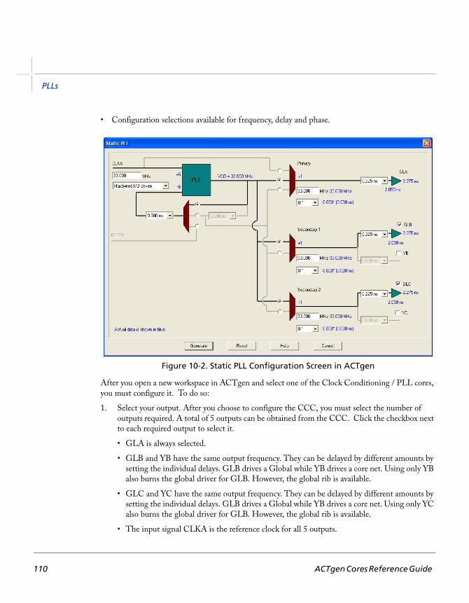
PLLs
• Configuration selections available for frequency, delay and phase.
Figure 10-2. Static PLL Configuration Screen in ACTgen
After you open a new workspace in ACTgen and select one of the Clock Conditioning / PLL cores, you must configure it. To do so:
1. Select your output. After you choose to configure the CCC, you must select the number of outputs required. A total of 5 outputs can be obtained from the CCC. Click the checkbox next to each required output to select it.
• GLA is always selected.
• GLB and YB have the same output frequency. They can be delayed by different amounts by setting the individual delays. GLB drives a Global while YB drives a core net. Using only YB also burns the global driver for GLB. However, the global rib is available.
• GLC and YC have the same output frequency. They can be delayed by different amounts by setting the individual delays. GLB drives a Global while YB drives a core net. Using only YC also burns the global driver for GLB. However, the global rib is available.
• The input signal CLKA is the reference clock for all 5 outputs.
110 ACTgen Cores Reference Guide

Configure Clock Conditioning / PLL cores
2. Select your feedback.
• Internal Feedback: The source of the feedback signals will be the
VCO output signal, with 0 degree phase shift and zero additional time delay. (Top Selection on the Feedback MUX) OR
A delayed version of the VCO output, in selectable increments of 160 ps, up to 5.56 ns. This delay advances the feedback clock, thereby advancing all outputs by the delay value specified for the feedback delay element. (Middle selection of the Feedback MUX)
• External Feedback: The source of the feedback signals will be an external signal coming from an I/O (bottom selection of the Feedback MUX). In this case, the Feedback Delay element will not be accessible to further advance the feedback signal.
3. Set your Fixed System Delay. By choosing the non-zero value for this delay, the feedback source signal can be further delayed by a fixed amount of mask delay designed to emulate the delay through the chip’s clock tree. This allows for clock-line de-skewing operations.
4. Specify your input clock
• Input Clock Frequency between 1.5 – 350 MHz
• Input Clock Source as one of the following
Driven by the hardwired I/O
Driven by an external I/O from a different I/O location
Driven by an internal core net.
5. Specify primary output. Select source of the output clock.
Output bypassing the PLL (Top selection of the GLA MUX). In this case VCO phase shift and output frequency selection are not available. Output frequency is the same as input frequency in this case.
Output directly from the VCO (Middle selection of the GLA MUX). The phase shift of 0,90, 180 or 270 is available in this case.
Delayed version of the zero phase shift output from the VCO. Phase-shift selection is unavailable for this,the bottom selection of the GLA MUX This output can be used for two purposes: a) to use the feedback delay as an additional delay on the output if feedback advance has not been specified (top and bottom selections of the feedback MUX); b) to compensate for the feedback advance for this particular output if feedback advance has been specified (middle selection of the feedback MUX).
• Output frequency (1.5 – 350 MHz)
• VCO Phase-Shift (one of 0, 90, 180 or 270 degrees); the phase shift is out of the VCO. The phase shift will be impacted by the value of the divider after the VCO.
ACTgen Cores Reference Guide 111

PLLs
• An optional Extra Output Delay, in selectable increments of 160 ps, up to 5.56 ns.
6. Specify Secondary 1 & Secondary 2 Outputs. Select the source of the output clock from the following 2 choices
Output directly from the VCO (Top selection of the GLB/GLC MUX). The phase shift of 0, 90, 180 or 270 is available in this case.
Delayed version of the zero phase shift output from the VCO. Phase-shift selection is unavailable for this, the bottom selection of the GLB/GLC MUX. This output can be used for two purposes: a) to use the feedback delay as an additional delay on the output if feedback advance has not been specified (top and bottom selections of the feedback MUX); b) to compensate for the feedback advance for this particular output if feedback advance has been specified (middle selection of the feedback MUX).
• Set your Output frequency (1.5 – 350 MHz)
• VCO Phase-Shift (one of 0, 90, 180 or 270 degrees); the phase shift is out of the VCO. The phase shift will be impacted by the value of the divider after the VCO.
• An individual optional Extra Output Delay for each of the Global and Core outputs, in selectable increments of 160ps, up to 5.56ns.
Delayed Clock
When resources are available, the Delay element of the Secondary1 and Secondary2 Global outputs of the CCC can be configured independent of the PLL. The delayed clock is a simple CLKMUX with some additional delay.
Select the programmable delay between 0.4 to 4.275ns in steps of 125ps for the Output.
Clock Conditioning / PLL core restrictions in ACTgenClock conditioning and PLL cores are available only for ProASIC3/E devices.
After you make all your selections, ACTgen generates a core with your configurations. However, there are a number of restrictions in the possible values for the input and output frequencies. They are:
• Input to the clock conditioning core (CCC) must be between 1.5 and 350 MHz
• Output from the CCC must be between 1.5 and 350 MHz
• The reference input to the PLL core (fin/n) must be between 1.5 and 5.5 MHz. The PLL Core output must be between 24 and 350 (fin *m/n)
If ACTgen cannot generate the frequency you requested, it tries to generate a frequency that is the closest to the required one, after it satisfies all the above conditions. ACTgen prints a message in the log file indicating the frequency it was able to achieve.
112 ACTgen Cores Reference Guide

Configure Clock Conditioning / PLL cores
If more than one output is specified, ACTgen tries to find the multiplication and division factors such that the total error among all the outputs is the least.
Total Delays
ACTgen prints out the total delays of the selected outputs after feedback delay, feedback advance, system delay and extra output delay are taken into consideration.
Total Delay on an Output = -feedback advance – de-skew system delay + feedback delay + extra output delay + intrinsic delay
Input Delays
The delay between the input of the PLL and a given output can be calculated by the following equation:
Total Delay = Intrinsic delay +/- feedback delay – mask delay + phase delay + output delay
Intrinsic delay is the total delay of all the muxes and divider elements in the path. This is a fixed value for a given connectivity in a configuration. This delay varies based on the mux selection, frequency values and phase-shifts. Changing the delay element values has no impact on the intrinsic delay.
Feedback delay can be both a positive and a negative delay based on how it is configured.
Mask delay is a fixed system delay to emulate the skew of the CCC, such that the output can be deskewed by selecting this delay.
Output delay is the programmable delay independently selectable for each output. Phase delay is the shift caused in the output with respect to the input when the VCO output is shifted by one of the 4 possible values of 0, 90, 180 or 270 degrees. This is a function of both input and output frequencies.
The delay calculation is executed using the same values for ACTgen, the Simulation model and Timer such that, for typical, -2 parts under normal operating conditions, these numbers are identical. This enables you to fine-tune your delays by only adjusting the programmable output / feedback delays.
ACTgen Cores Reference Guide 113

PLLs
ACTgen ProASIC3/E PLL signal descriptions PLL signal descriptions apply only to ProASIC3/E devices.
Table 10-5. ACTgen PLL Signal Description
Name Size TypeRequired/ Optional
Function
GLA 1 Output Req Primary clock output
CLKA 1 Input Req Reference Clock
POWERDOWN 1 Input ReqPower Down Signal. A Low on this signal turns off the PLL
LOCK 1 Output Req PLL lock
EXTFB 1 Input Opt External Feedback
GLB 1 Output Opt Global Output for Secondary1 Clock
YB 1 Output Opt Core Output for Secondary1 Clock
GLC 1 Output Opt Global Output for Secondary2 Clock
YC 1 Output Opt Core Output for Secondary2 Clock
114 ACTgen Cores Reference Guide

11Register (Storage Elements)
ACTgen Cores Reference Guide 115

Storage Register
Features• Parameterized word length
• Asynchronous clear
• Synchronous register parallel load
• Behavioral simulation model in VHDL and Verilog
Family SupportACT 1, ACT 2/1200XL, ACT 3, 3200DX, 40MX, 42MX, 54SX, 54SX-A, eX, 500K, PA, Axcelerator, ProASIC3/E
DescriptionStorage registers have a parallel-in/parallel-out (PIPO) architecture. The registers are WIDTH bits. They are clocked on the rising (RISE) or falling (FALL) edge of the clock Clock (CLK_EDGE).
The Clear signal (CLR_POLARITY), active high or low, provides an asynchronous reset of the registers to “000…0”. You may choose to not implement the reset function.
The Enable signal (EN_POLARITY), active high or low, provides a synchronous load enable operation with respect to the Clock signal. You can choose to not implement this function. Storage registers are then loaded with a new value every clock cycle.
The Set signal, active high or low, provides an asynchronous set of the registers to "1111...1". You may choose not to implement the Set function.
Enable
Set (PA and 500K only)
Clock
Q
Aclr
Data
Table 11-1. Port Description
Port Name
Size Type Req./Opt. Function
Data WIDTH input Req. Register load input
Aclr 1 input Opt. Asynchronous register reset
Enable 1 input Opt. Synchronous Parallel load enable
Clock 1 input Req. Clock
Q WIDTH output Req. Register output bus
ACTgen Cores Reference Guide 116

Table 11-2. Parameter Description
Parameter Family Value Function
WIDTH500K, PA 1-512
Word length of Data and QAll other 1-99
CLR_POLARITY ALL 0 1 2 Aclr can be active low, active high or not used
EN_POLARITY ALL 0 1 2 Enable can be active low, active high
CLK_EDGE ALLRISE
FALLClock can be rising or falling
Table 11-3. Fan-in Control Parameters
Parameter Value
CLR_FANIN AUTO MANUAL
CLR_VAL <val> [default value for AUTO is 8, 1 for MANUAL]
EN_FANIN AUTO MANUAL
EN_VAL <val> [default value for AUTO is 6, 1 for MANUAL]
CLK_FANIN AUTO MANUAL
CLK_VAL <val> [default value for AUTO is 8, 1 for MANUAL]
Table 11-4. Implementation Parameters
Parameter Value Description
LPMTYPE LPM_DFF Register category
LPM_HINT PIPO Parallel-in/Parallel-out
ACTgen Cores Reference Guide 117

Register (Storage Elements)
Table 11-5. Functional Descriptiona
a. Assume Aclr is active low, Enable is active high, Clock is rising (edge-triggered)
Data Aclr Enable Clock Q
X 0 X X 0’s
X 1 X Ø Qn
X 1 0 ¦ Qn
m 1 1 ¦ Qn+1 = m
118 ACTgen Cores Reference Guide

Shift Register
Features• Parameterized word length
• Asynchronous clear
• Synchronous parallel load
• Behavioral simulation model in VHDL and Verilog
Family SupportACT 1, ACT 2/1200XL, ACT 3, 3200DX, 40MX, 42MX, 54SX, 54SX-A, eX, 500K, PA, Axcelerator, ProASIC3/E
DescriptionShift registers have parallel-in/parallel-out (PIPO), parallel-in/serial-out (PISO), serial-in/parallel-out (SIPO) and serial-in/serial-out (SISO) architecture. The registers are WIDTH bits. They are clocked on the rising (RISE) or falling (FALL) edge of the clock Clock signal (CLK_EDGE).
The Clear signal (CLR_POLARITY), active high or low, provides an asynchronous reset of the registers to “000…0”. You may choose to not implement the reset function.
Shift registers can be loaded with Data. The Enable signal (EN_POLARITY), active high or low, provides a synchronous load enable operation with respect to the clock signal Clock. You may choose to not implement this function. Shift registers are then implemented in a serial-in mode (SIPO or SISO).
Shift registers have a shift enable signal Shiften (SHEN_POLARITY) that can be active high or low. When Shiften is active, the register is shifted internally. The LSB is loaded with Shiftin.
In the current implementation, Enable has priority over Shiften.
Data
Shiftin
Enable
Clock
Q
Shiftout
Aclr
Shiften
Table 11-6. Port Description
Port Name
Size Type Req/Opt Function
Data WIDTH input Opt. Register load input data
Shiftin 1 Input Opt. Shift in signal
Aclr 1 input Opt. Asynchronous register reset
Enable 1 input Opt. Synchronous parallel load enable
ACTgen Cores Reference Guide 119

Register (Storage Elements)
Shiften 1 input Req. Synchronous register shift enable
Clock 1 input Req. Clock
Q WIDTH output Opt. Register output bus
Shiftout 1 output Opt. Serial output
Table 11-7. Parameter Description
Parameter Family Value Function
WIDTH500K, PA 2-512
Word length of Data and QAll other 2-99
CLR_POLARITY ALL 0 1 2Aclr can be active low, active high or not used
EN_POLARITY ALL 0 1 2 Enable can be active low, active high
SHEN_POLARITY ALL 0 1Shiften can be active low, active high or not used
CLK_EDGE ALLRISE FALL
Clock can be rising or falling
Table 11-8. Fan-in Control Parameters
Parameter Value
CLR_FANIN AUTO MANUAL
CLR_VAL <val> [default value for AUTO is 8, 1 for MANUAL]
EN_FANIN AUTO MANUAL
EN_VAL <val> [default value for AUTO is 6, 1 for MANUAL]
SHEN_FANIN AUTO MANUAL
SHEN_VAL <val> [default value for AUTO is 6, 1 for MANUAL]
Table 11-6. Port Description (Continued)
Port Name
Size Type Req/Opt Function
120 ACTgen Cores Reference Guide

CLK_FANIN AUTO MANUAL
CLK_VAL <val> [default value for AUTO is 8, 1 for MANUAL]
Table 11-9. Implementation Parameters
Parameter Value Description
LPMTYPE LPM_DFF Register category
LPM_HINT PIPOS Parallel-in/Parallel-out shift register
PISO Parallel-in/Serial-out shift register
SIPO Serial-in/Parallel-out shift register
SISO Serial-in/Serial-out shift register
Table 11-10. Functional Descriptiona
a. Aclr is active low, Enable is active high, Shiften is active high, Clock is rising.
Data Aclr Enable Shiften Clock Qb
b. For the PISO and SISO implementations, Q is an internal register.
Shiftoutc
c. For the PIPO and SIPO implementations, Shiftout is not present.
X 0 X X X 0 0
X 1 X X Ø Qn Qn = [WIDTH-1]
X 1 0 0 ¦ Qn Qn = [WIDTH-1]
X 1 0 1 ¦ Qn[ WIDTH-2:0] && Shiftin Qn = [WIDTH-1]
m 1 1 X ¦ Qn+1 = m Qn+1 = m[WIDTH-1]
Table 11-8. Fan-in Control Parameters (Continued)
Parameter Value
ACTgen Cores Reference Guide 121

Barrel Shifter
Features• Parameterized word length
• Standard or pipelined
• Shift right, left or both
• Wrap around or feed bit
• Fixed or programmable shift.
Family Support54SX, 54SX-A, eX, 500K, PA, Axcelerator, ProASIC3/E
DescriptionThe Barrel Shifter can be generated for a fixed shift or range of shift, with feedbit shift or rotation in left, right, or both directions. The non-pipelined Barrel Shifter is designed to shift any number of positions at one time. For the pipelined version it takes log2(MAXSHIFT) clock cycles for the shifted data to appear at the output.
The architecture is based on 2 to 1 Multiplexors.
Data
Enable
Clock
Q
Aclr
Dir
Table 11-11. Port Description
Port Name
Size Type Req./Opt. Function
Data WIDTH input Req. Register load input
Aclr 1 input Opt. Asynchronous register reset
Dir 1 input Opt For selecting Left or Right shift
RFill 1 input Opt For Right Feed Bit
LFill 1 input Opt For Left Feed Bit
S0, S1…Log of
Max. Shiftinput Opt
For programmable, depends on Maximum
shift
Enable 1 input Opt. Synchronous Parallel load enable
Clock 1 input Req. Clock
Q WIDTH output Req. Register output bus
ACTgen Cores Reference Guide 122

s
Table 11-12. Parameter Description
Parameter Value Function
WIDTH
2-99 (Pipelined)2-63 (Standard)2-99 (PA fixed programmable) 2-63 (PA range programmable
Word length of Data and Q
MAXSHIFT 1-32 Maximum Shift length
CLR_POLARITY 0 1 2 Aclr can be active low, active high or not used
PROG Fixed or Range For a Fixed or Programmable shift
FILL No, Yes Wrap around or Feed a bit
DIRECTION Right Left Both Direction can be Right Left or Both
EN_POLARITY 0 1 2 Enable can be active low, active high
CLK_EDGE RISE FALL Clock can be rising or falling
Table 11-13. Fan-in Control Parameters
Parameter Value
CLR_FANIN AUTO MANUAL
CLR_VAL <val> [ default value for AUTO is 8, 1 for MANUAL]
EN_FANIN AUTO MANUAL
EN_VAL <val> [ default value for AUTO is 6, 1 for MANUAL]
CLK_FANIN AUTO MANUAL
CLK_VAL <val> [ default value for AUTO is 8, 1 for MANUAL]
SEL0_FANIN AUTO MANUAL
SEL0_VAL <val> [ default value for AUTO is 6, 1 for MANUAL]
ACTgen Cores Reference Guide 123

Register (Storage Elements)
Table 11-14. Implementation Parameters
Parameter Value Description
LPMTYPE LPM_DFF Register category
LPM_HINT SHIFT, PIPE Standard or Pipelined
Table 11-15. Functional Descriptiona (Standard)
a. Assume Aclr is active low, Enable is active high, Clock is rising
Data Enable Clock Q
M 1 ¦ Qn
M 0 ¦ Mshifted
Table 11-16. Functional Descriptiona (Pipelined)
a. Assume Aclr is active low, Enable is active high, Clock is rising
Data Aclr Enable Clock Q
X 0 X X 0’s
X 1 0 X Qn = Mshifted - log2(MAXSHIFT)
M 1 1 ¦ Qn+1 = Mshifted - log2(MAXSHIFT) + 1
124 ACTgen Cores Reference Guide

Storage Latch
Features• Parameterized word length
• Asynchronous clear
• Synchronous latch enable
• Behavioral simulation model in VHDL and Verilog
Family SupportACT 1, ACT 2/1200XL, ACT 3, 3200DX, 40MX, 42MX 54SX, 54SX-A, eX, 500K, PA, Axcelerator, ProASIC3/E
DescriptionLatches have a parallel-in/parallel-out architecture (PIPO). The latches are WIDTH bits. The latches are gated on the active high (HIGH) or low (LOW) state of the gate Gate (GATE_POLARITY).
The Clear signal (CLR_POLARITY), when active high or low, provides an asynchronous reset of the latch to “000…0”. You may choose to not implement this function.
The Enable signal (EN_POLARITY), when active high or low, provides a synchronous latch enable operation with respect to the gate Gate. You may choose to not implement this function. Latches are then loaded with a new value when both Enable and Gate are active.
Enable
Gate
Q
Aclr
Data
Table 11-17. Port Description
Port Name
Size Type Req/Opt Function
Data WIDTH input Req. Latch load input
Aclr 1 input Opt. Asynchronous latch reset
Enable 1 input Opt. Synchronous parallel latch enable
Gate 1 input Req. Gate input
Q WIDTH output Req. Latch output bus
ACTgen Cores Reference Guide 125

Register (Storage Elements)
Table 11-18. Parameter Description
Parameter Family Value Function
WIDTH500K, PA 1-99
Word length of Data and QAll other 1-512
CLR_POLARITY ALL 0 1 2Aclr can be active low, active high or not used
EN_POLARITY ALL 0 1 2 Enable can be active low, active high
GATE_POLARITY ALL 0 1 Gate can be active low, or active high
Table 11-19. Fan-in Control Parameters
Parameter Value
CLR_FANIN AUTO MANUAL
CLR_VAL <val> [default value for AUTO is 8, 1 for MANUAL]
EN_FANIN AUTO MANUAL
EN_VAL <val> [default value for AUTO is 6, 1 for MANUAL]
GATE_FANIN
AUTO MANUAL
GATE_VAL <val> [default value for AUTO is 8, 1 for MANUAL]
Table 11-20. Implementation Parameters
Parameter Value Description
LPMTYPE LPM_LATCH Latch category
LPM_HINT N/A Not needed
126 ACTgen Cores Reference Guide

Table 11-21. Functional Descriptiona
a. Assume Aclr is active low, Enable is active high, Gate is active high
Data Aclr Enable Gate Q
X 0 X X 0’s
X 1 X 0 Qn
X 1 0 1 Qn
m 1 1 1 Qn+1 = m
ACTgen Cores Reference Guide 127

Register (Storage Elements)
128 ACTgen Cores Reference Guide
12Memory Cores for Non-Axcelerator Families
ACTgen Cores Reference Guide 129

Synchronous/Asynchronous Dual Port RAM
Features• Parameterized word length and depth• Dual port synchronous RAM architecture• Dual port synchronous write, asynchronous read RAM
architecture
Family Support3200DX, 42MX
DescriptionThe RAM cores use 3200DX and 42MX, 32x8 or 64x4, dual port RAM cells.
In the synchronous mode, the read and write operations are totally independent and can be performed simultaneously. The operation of the RAM is fully synchronous with respect to the clock signals, WClock and RClock. Data of value Data are written to the WAddress of the RAM memory space on the rising (RISE) or falling (FALL) edge of the clock WClock (WCLK_EDGE). Data are read from the RAM memory space at RAddress into Q on the rising (RISE) or falling (FALL) edge of the clock signal RClock (RCLK_EDGE).
The behavior of the RAM is unknown if you write and read at the same address and signals WClock and RClock are not the same. The output Q of the RAM depends on the time relationship between the write and the read clock.
In the asynchronous mode, the operation of the RAM is only synchronous with respect to the clock signal WClock. Data of value Data are written to the WAddress of the RAM memory space on the rising (RISE) or falling (FALL) edge of the clock signal WClock (WCLK_EDGE). Data are read from the RAM memory space at RAddress into Q after some delay when RAddress has changed.
The behavior of the RAM is unknown if you write and read at the same address. The output Q depends on the time relationship between the write clock and the read address signal.
The WIDTH (word length) and DEPTH (number of words) have continuous values but the choice of WIDTH limits the choice of DEPTH and vice versa.
Data
WClock
WAddress
RAddress
RClock
WE
RE
Q
ACTgen Cores Reference Guide 130

The write enable (WE) and read enable (RE) signals are active high request signals for writing and reading, respectively; you may choose not to use them.
Table 12-1. Port Description
Port Name
Size Type Req/Opt Function
Data WIDTH input Req. Input Data
WE 1 input Opt. Write Enable
RE 1 input Opt. Read Enable
WClock 1 input Req. Write clock
RClock 1 input Opt. Read clock
Q WIDTH output Req. Output Data
Table 12-2. Parameter Description
Parameter Value Function
WIDTH width Word length of Data and Q
Depth depth Number of RAM words
WE_POLARITY 1 2 WE can be active high or not used
RE_POLARITY 1 2 RE can be active high or not used
WCLK_EDGE RISE FALL WClock can be rising or falling
RCLK_EDGE RISE FALL NONE RClock can be rising, falling or not used
Table 12-3. Implementation Parameters
Parameter Value Description
LPMTYPE LPM_RAM_DQ Generic Dual Port RAM category
ACTgen Cores Reference Guide 131

Memory Cores for Non-Axcelerator Families
Fan-in ControlOne of the key issues when building RAM cores is control of the routing congestion near the RAM cells. The problem becomes more critical when deep RAM cores are built. You need to broadcast signals throughout the height of the chip. The place-and-route algorithm could have difficulties satisfying all routing constraints. As a result, much slower routing resources could be allocated to satisfy all constraints. To make this problem less likely, a special buffering scheme has been implemented to relieve the congestion near the RAM cells. However, you may choose to control the buffering yourself to improve performances when needed. The RAM core can be built using either the automatic buffering architecture or the manual buffering architecture.
Table 12-4. Fan-in Parameters
Parameter Value Description
RAMFANIN AUTO MANUAL See Fan-in Control section below
Table 12-5. Parameter Rules
Parameter Rules
If RCLK_EDGE is NONE (Asynchronous mode), then RE_POLARITY must be 2 (note used)
The number of RAM blocks used (function of width and depth) must be less than or equal to the number of RAM blocks in one column of the largest device.
132 ACTgen Cores Reference Guide

Automatic Buffering
In this mode (default), a buffering scheme is automatically built into the RAM core architecture (see Figure 12-1 on page 133). This mode should always be considered first. However, if the performance is not met, it may be better to use the manual buffering option .
Figure 12-1. Automatic Buffering for RAM Cores
Manual Buffering
Figure 12-2 shows how manual buffering is done. A fan-in of one (1) is enforced on all signals fanning out to more than one RAM cell. If these signals were broadcast to all RAM cells, very slow routing resources (long freeways) would be required to route the signals impacting the RAM performance.
Use Manual Buffering only if the expected performance is not realized using the automatic buffering scheme, or if you know ahead of time that you need to use this scheme to meet your timing goals. In this architecture, the idea is not to buffer the signals internally but rather give some kind of access to the RAM core internal signals. Then, you must buffer the signals outside the core and either use traditional buffers or duplicate the logic that drives these signals externally. If you choose manual buffering, the WE, RE, Waddress(i), RAddress(i) and Data[i] signals become busses external to the core. For all these signals, the bus width is equal to the number of RAM cells (used to build a given configuration) driven by each signal. Figure 12-2 illustrates the manual buffering architecture for a 96x8 RAM configuration, built of three 32x8 configured RAM cells. In this configuration, the WE, RE, WAddress and RAddress signals drive all RAM cells simultaneously. Figure 12-3 shows a 128x8
RAM
RAM
RAM
1
1
1
WEREWAdress[i]RAdress[i]Data
ACTgen Cores Reference Guide 133

Memory Cores for Non-Axcelerator Families
RAM configuration, built using four 64x4 configured RAM cells. In that configuration, the 8-bit data bus is split into two completely independent 4-bit data busses.
Figure 12-2. Manual Buffering (96x8 RAM Configuration)
Figure 12-3. Manual Buffering for the Data Bus (128x8 RAM Configuration)
Timing Waveforms
RAM
RAM
RAM
1
1
1
WEREWAdress[i]RAdress[i]Data
1
1
RAM
RAM
1
1
RAM
RAM
Data (i) [1:0]
Data (i+4) [1:0]
Table 12-6. Timing Waveform Terminology
Term Description Term Description
tckhl Clock high/low period tdsu Data setup time
134 ACTgen Cores Reference Guide

Figure 12-4. RAM Write Cycle
trp Reset pulse width trco Data valid after clock high/low
twesu Write enable setup time traoData valid after read address has changed
tresu Read enable setup time tco Flip-flop clock to output
Table 12-6. Timing Waveform Terminology
Term Description Term Description
WClock
Data
WE
Data latched into FIFO
dsu
wesu
ckhl tckhl
t
t
t t
ACTgen Cores Reference Guide 135

Memory Cores for Non-Axcelerator Families
Figure 12-5. RAM Synchronous Read Cycle
Figure 12-6. RAM Asynchronous Read Cycle
Valid Output
RClock
Q
RE
resu
ckhl tckhl
rco
t
t t
t
Q
RAddress
Valid Output
t rao
136 ACTgen Cores Reference Guide

Register File
Features • Parameterized word length and depth
• Dual port synchronous RAM architecture
• Dual port synchronous write, asynchronous read RAM architecture
• Write and Read enable
• Behavioral simulation model in VHDL and Verilog
Family Support54SX, 54SX-A, eX
DescriptionThe register file is a core unique to the 54SX, 54SX-A and eX families. This core synthesizes the equivalent of small RAM blocks using ordinary logic, thereby making memory cells available to yosu even though the silicon does not explicitly have hardware support for RAM.
In synchronous mode, the read and write operations are totally independent and can be performed simultaneously. The operation of the register is fully synchronous with respect to the clock signals WClock and RClock. Data of value Data are written to the WAddress of the register memory space on the rising (RISE) or falling (FALL) edge of the clock WClock (WCLK_EDGE). Data are read from the register memory space at RAddress into Q on the rising (RISE) or falling (FALL) edge of the clock RClock (RCLK_EDGE).
The behavior of the Register is unknown, if designers write and read at the same address and WClock and RClock are not the same. The output Q of the register depends on the time relationship between the write and the read clock.
In asynchronous mode, the operation of the register is only synchronous with respect to the clock signal WClock. Data of value Data are written to the WAddress of the register memory space on the rising (RISE) or falling (FALL) edge of the clock WClock (WCLK_EDGE). Data are read from the register memory space at RAddress into Q after some delay when RAddress has changed.
The WIDTH (word length) and DEPTH (number of words) have continuous values but the choice of WIDTH limits the choice of DEPTH and vice versa.
The write enable (WE) and read enable (RE) signals are active high request signals for writing and reading, respectively. The user may not utilize them.
Data
WClock
RClock
WE
Q
REnableRAdress
WAdress
ACTgen Cores Reference Guide 137

Memory Cores for Non-Axcelerator Families
Table 12-7. Port Description
Port Name Size Type
Data WIDTH input
WE 1 input
RE 1 input
WClock 1 input
RClock 1 input
Q WIDTH output
Table 12-8. Parameter Description
Parameter Value Function
WIDTH width Word length of Data and Q
DEPTH depth Number of RAM words
WE_POLARITY
1 2 WE can be active high or not used
RE_POLARITY 1 2 RE can be active high or not used
WCLK_EDGE RISE FALL WClock can be rising or falling
RCLK_EDGERISE FALL NONE
RClock can be rising, falling or not used
138 ACTgen Cores Reference Guide

Timing Waveforms
Figure 12-7. Ram Write Cycle
Table 12-9. Timing Waveform Terminology
Term
Description Term Description
tckhl Clock high/low period tdsu Data setup time
trp Reset pulse width trco Data valid after clock high/low
twesu Write enable setup time traoData valid after read address has changed
tresu Read enable setup time tco Flip-flop clock to output
WClock
Data
WE
tadsu
twesu
tckhl ttckhl
WAddress
twadsu
Data latched into RAM
ACTgen Cores Reference Guide 139

Memory Cores for Non-Axcelerator Families
Figure 12-8. RAM Synchronous Read Cycle
Figure 12-9. RAM Asynchronous Read Cycle
RClock
Q
RE
tresu
tckhl ttckhl
RAddress
tradsu
Valid Output
trco
Q
RAddress
Valid Output
trao
140 ACTgen Cores Reference Guide

Synchronous Dual Port FIFO without Flags
Features• On-chip RAM
• Parameterized word length and depth
• Dual port synchronous FIFO (write and read clocks are separated) with no static flag logic
• Global reset of FIFO address pointers
Family Support3200DX, 42MX, 54SX, 54SX-A, eX
DescriptionThe ACTgen FIFO cores use the 3200DX and 42MX 32x8 or 64x4 on-chip RAM cells. ACTgen generates addresses internally using counters and token chains to address the RAM blocks (transparent to the user). Dedicated read and write address data paths are used in the FIFO architecture. The read and write operations are independent and can be performed simultaneously.
The WIDTH (word length) and DEPTH (number of words) have continuous values but the choice of WIDTH limits the choice of DEPTH and vice versa.
The asynchronous clear signal, Aclr, can be active low or active high (low is the default option and is the preferred use for all synchronous elements in the two supported families). When the asynchronous clear is active, all internal registers used to determine the current FIFO read and write addresses (counters and token chains) are reset to “0.” The FIFO is now in an empty state; the RAM content is not affected. When power is first applied to the FIFO, the FIFO must be initialized with an asynchronous clear cycle to reset the internal address pointers.
The write enable WE and read enable RE signals are active high request signals for writing into and reading out of the FIFO respectively. The WE and RE signals only control the logic associated with the FIFO write and read address pointers.
When WE is asserted high, the write cycle is initiated, and Data are written into the FIFO. The design using the FIFO is responsible for handling the full and empty states of the FIFO core.
When RE is asserted high, the read cycle is initiated, and Q is read from the FIFO. The design using the FIFO is responsible for handling the full and empty states of the FIFO core.
WE
RClock
Q
Aclr
Data
RE
WClock
ACTgen Cores Reference Guide 141

Memory Cores for Non-Axcelerator Families
Table 12-10. Port Description
Port Name
Size Type Req/Opt Function
Data WIDTH input Req. Input Data
WE 1 input Req. Write Enable
RE 1 input Req. Read Enable
WClock 1 input Req. Write clock
RClock 1 input Req. Read clock
Q WIDTH output Req. Output Data
Table 12-11. Parameter Description
Parameter Value Function
WIDTH width Word length of Data and Q
DEPTH depth Number of FIFO words
WCLK_EDGE RISE FALL WClock can be rising or falling
RCLK_EDGE RISE FALL RClock can be rising falling
Table 12-12. Implementation Parameters - MX/DX
Parameter Value Description
LPMTYPE LPM_FIFO_DQ Generic FIFO category
LPM_HINT SFIFO Synchronous FIFO with no flags
142 ACTgen Cores Reference Guide

Timing Waveforms
Table 12-13. Implementation Parameters - 54SX/SX-A
Parameter Value Description
LPM_HINT SFIFOSX Synchronous FIFO with no flags
Table 12-14. Fan-in Parameters
Parameter Value Description
RAMFANIN AUTO MANUAL See “Fan-in Control” on page 132
Table 12-15. Timing Waveform Terminology
Term
Description Term Description
tckhl Clock high/low period tdsu Data setup time
trp Reset pulse width trco Data valid after clock high/low
twesu Write enable setup time tco Flip-flop clock to output
tresu Read enable setup time
ACTgen Cores Reference Guide 143

Memory Cores for Non-Axcelerator Families
Figure 12-10. FIFO Write Cycle
Figure 12-11. FIFO Read Cycle
WClock
Data
WE
Data latched into FIFO
t
t
t t
dsu
wesu
ckhl tckhl
RClock
Q
RE
Valid Output
t
t t
t
resu
ckhl tckhl
rco
144 ACTgen Cores Reference Guide
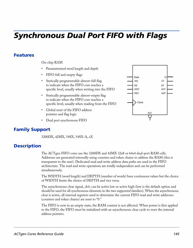
Synchronous Dual Port FIFO with Flags
FeaturesOn-chip RAM
• Parameterized word length and depth
• FIFO full and empty flags
• Statically programmable almost-full flag to indicate when the FIFO core reaches a specific level, usually when writing into the FIFO
• Statically programmable almost-empty flag to indicate when the FIFO core reaches a specific level, usually when reading from the FIFO
• Global reset of the FIFO address pointers and flag logic
• Dual port synchronous FIFO
Family Support3200DX, 42MX, 54SX, 54SX-A, eX
DescriptionThe ACTgen FIFO cores use the 3200DX and 42MX 32x8 or 64x4 dual-port RAM cells. Addresses are generated internally using counters and token chains to address the RAM (this is transparent to the user). Dedicated read and write address data paths are used in the FIFO architecture. The read and write operations are totally independent and can be performed simultaneously.
The WIDTH (word length) and DEPTH (number of words) have continuous values but the choice of WIDTH limits the choice of DEPTH and vice versa.
The asynchronous clear signal, Aclr, can be active low or active high (low is the default option and should be used for all synchronous elements in the two supported families). When the asynchronous clear is active, all internal registers used to determine the current FIFO read and write addresses (counters and token chains) are reset to “0.”
The FIFO is now in an empty state; the RAM content is not affected. When power is first applied to the FIFO, the FIFO must be initialized with an asynchronous clear cycle to reset the internal address pointers.
Data
Clock
WE
RE
Q
Aclr
WEF
REF
FF
EF
AFF
AEF
ACTgen Cores Reference Guide 145

Memory Cores for Non-Axcelerator Families
The full flag signal, FF, is optional and is available only for the High Speed Flag (FFIFO) and the Medium Speed Flag (MFFIFO) variations. The FF signal is active high only (if selected) and indicates when the FIFO is full. The signal is asserted high on the rising (RISE) or falling (FALL) edge of the clock signal Clock with no delay.
The empty flag signal, EF, is optional and is available only for the High Speed Flag (FFIFO) and the Medium Speed Flag (MFFIFO) variations. The EF signal is active low only (if selected) and indicates when the FIFO is empty. The signal is asserted low on the rising (RISE) or falling (FALL) edge of the clock signal Clock with no delay.
The write enable signals, WE and WEF, and read enable signals, RE and REF, are active high requests for writing into and reading out of the FIFO respectively. The WE and RE signals only control the logic associated with the FIFO write and read address pointers. The WEF and REF signals control the logic implementing the different flags. The WE and WEF signals should be logically driven by the same logic outside the FIFO core. The same behavior applies to the RE and REF signals as well. For SX and SX-A there are only the RE and WE ports.
When WE is asserted high and FF is asserted low (not full), the write cycle is initiated and Data are written into the FIFO. When WE is asserted high and FF is asserted high (full), the FIFO behavior is undefined. When RE is asserted high and EF is asserted high (empty), the read cycle is initiated and Q is read from the FIFO. When RE is asserted high and EF is asserted low (empty), the FIFO behavior is undefined. When RE and WE are asserted high at the same time, Data are written into the FIFO and Q is read from the FIFO simultaneously. The read and write operations are fully synchronous with respect to the clock signal Clock.
The FIFO function offers a parameterizable almost-full flag, AFF. The AFF flag is asserted high when the FIFO contains aff_val words or more as defined by the parameter AFF_VAL. Otherwise, AFF is asserted low. The aff_val value is a parameter to the core, and thus logic is built at generation time to realize the almost-full flag function.
The FIFO function offers a parameterizable almost-empty flag, AEF. The AEF flag is asserted low when the FIFO contains aef_val words or less as defined by the parameter AEF_VAL. Otherwise, AEF is asserted high. The aef_val value is a parameter to the core, and thus logic is built at generation time to realize the almost-empty flag function.
Table 12-16. Port Description
Port Name
Size Type Req./Opt. Function
Data WIDTH input Req. Input Data
WE 1 input Req. Write Enable with the FIFO only (noflag)
146 ACTgen Cores Reference Guide

RE 1 input Req. Read Enable with the FIFO only (no flag)
WEF 1 input Req.Write enable associated with the flag logic only (for DX/MX)
REF 1 input Req.Read enable associated with the flag logic only (for DX/MX)
Clock 1 input Req. Write and read clock
Q WIDTH output Req. Output Data
FF 1 output Req. Full Flag
EF 1 output Req. Empty Flag
AFF 1 output Optional Almost Full Flag
AEF 1 output Optional Almost Empty Flag
Table 12-17. Parameter Description
Parameter Value Function
WIDTH width Word length of Data and Q
DEPTH depth Number of FIFO words
FF_POLOARITY 1 2 FF can be active high or not
EF_POLARITY 0 2 EF can be active low or not used
AFF_VALaff_val (see parameter rules)
AFF value (not used if aff_val is 0
AEF_VALaef_val (see parameter rules
AEF value (not used if aef_val is 0
CLK_EDGE RISE FALL Clock can be rising or falling
Table 12-16. Port Description
Port Name
Size Type Req./Opt. Function
ACTgen Cores Reference Guide 147

Memory Cores for Non-Axcelerator Families
Timing Waveforms
Table 12-18. Implementation Parameters - MX/DX
Parameter Value Description
LPMTYPE LPM_FIFO_DQ Generic FIFO category
LPM_HINTFFIFO High skpeed FIFO with flags
MFFIFO Medium speed FIFO with flags
Table 12-19. Implementation Parameters - 54SX/SX-A
Parameter Value Description
LPM_HINT FFIFOSX Synchronous FIFO with no flags
Table 12-20. Fan-in Parameters
Parameter Value Description
RAMFANIN AUTO MANUAL See Fan-in Control section below
Table 12-21. Parameter Rules
Parameter Rules
If RCLK_EDGE is NONE (Asynchronous mode), then RE_POLARITY must be 2 (not used)
Table 12-22. Timing Waveform Terminology
Term Description
tckhl Clock high/low period
148 ACTgen Cores Reference Guide

Figure 12-12. Reset Cycle
trp Reset pulse width
twesu Write enable setup time
tresu Read enable setup time
tadsu Data setup time
trco Data valid after lock high/low
trao Data valid after read address has changed
tco Flip-flop clock to output
Table 12-22. Timing Waveform Terminology
Term Description
Clock
Aclr
FF
AEF
AFF
EF
tckhl ttckhl
trp
ACTgen Cores Reference Guide 149

Memory Cores for Non-Axcelerator Families
Figure 12-13. Write and Read Cycle
Figure 12-14. Full FIFO Timing Diagram
Clock
Q
WE/WEF
Data
Valid Output
trco
RE/REFtresu
tdsu
twesu
tchkl ttchkl
Clock
WE/WEF
RE/REF
FF
t
t t
t t
t
wesu
ckhl tckhl
co co
resu
150 ACTgen Cores Reference Guide

Figure 12-15. Empty FIFO Timing Diagram
Figure 12-16. Almost Full FIFO Timing Diagram
Clock
RE/REF
WE/WEF
EF
tresu
tckhl ttckhl
tco tco
twesu
Clock
WE/WEF
RE/REF
AFF
N writesN reads
tresu
tco
twesu
tco
ttckhltckhl
ACTgen Cores Reference Guide 151

FIFO Flag Controller (No RAM)
Features• Off-chip RAM
• Parameterized word length and depth
• FIFO full and empty flags
• Statically programmable almost-full flag to indicate when the FIFO core reaches a specific level,usually when writing into the FIFO
• Statically programmable almost-empty flag to indicate when the FIFO core reaches a specific level,usually when reading from the FIFO
• Global reset of the FIFO address pointers and flag logic
Family Support3200DX, 42MX, 54SX, 54SX-A, eX
DescriptionThe ACTgen FIFO Flag Controler is designed for off-chip RAM. It is a state machine generating the Flags typically used by a FIFO.
The asynchronous clear (Aclr) can be active low or active high (low is the default option and should be preferably used as for all synchronous elements in the two supported families). We will further use the word active to specify the state of a given signal. When the asynchronous clear is active, all internal registers are reset to '0'. The FIFO Controler is now in an empty state. At power up time, the FIFO must be initialized with a asynchronous clear cycle.
The full flag signal FF is optional. The FF signal is active high only (if selected) and indicates when the FIFO is full. The signal is asserted high on the rising (RISE) or falling (FALL) edge of the clock signal Clock with no delay.
The empty flag signal EF is optional. The EF signal is active low only (if selected) and indicates when the FIFO is empty. The signal is asserted low on the rising (RISE) or falling (FALL) edge of the clock signal Clock with no delay.
The write enable (WE) and read enable (RE) signals are active high requests signals for for controlling the FIFO flags. They should be logically equivalent to the write and read enable controlling the off-chip RAM.
Clock
WE
RE
Aclr
FF
EF
AFF
AEF
ACTgen Cores Reference Guide 152

The FIFO Controller offers a parameterizable almost-full flag (AFF). The AFF flag is asserted high when the FIFO contains aff_val words or more as defined by the parameter AFF_VAL. Otherwise, AFF is asserted low. The value aff_val value is a parameter to the core, and thus logic is built at generation time to realize the almost-full flag function.
The FIFO Controller offers a parameterizable almost-empty flag (AEF). The AEF flag is asserted low when the FIFO contains aef_val words or less as defined by the parameter AEF_VAL. Otherwise, AEF is asserted high. The value aef_val value is a parameter to the core, and thus logic is built at generation time to realize the almost-empty flag function.
Table 12-23. Port Description
Port Name
Size Type Req/Opt? Function
Clock 1 input Req. Write and read clock
WE 1 input Req. Write enable associated to the flag logic only
RE 1 input Req. Read enable associated to the flag logic only
Aclr 1 input Req. Asynchronous Clear
EF 1 output Opt. Empty Flag
FF 1 output Opt. Full Flag
AEF 1 output Opt. Almost Empty Flag
AFF 1 output Opt. Almost Full Flag
Table 12-24. Parameter Description
Parameter Value Function
WIDTH width Word length of Data and Q
DEPTH depth Number of FIFO words
FF_POLARITY 1 2 FF can be active high or not used
EF_POLARITY 0 2 EF can be active low or not used
AFF_VAL aff_val (see parameter rules) AFF value (not used if aff_val is 0)
ACTgen Cores Reference Guide 153

Memory Cores for Non-Axcelerator Families
AEF_VAL aef_val (see parameter rules) AEF value (not used if aef_val is 0)
CLK_EDGE RISE FALL Clock can be rising or falling
Table 12-25. Implementation Parameters - MX/DX
Parameter Value Description
LPMTYPE LPM_FIFO_DQ Generic FIFO category
LPM_HINTFFIFOCTRL High speed FIFO Controller
MFFIFOCTRL Medium speed FIFO Controller
Table 12-26. Implementation Parameters - 54SX/SX-A/eX
Parameter Value Description
LPM_HINT FCTR FIFO Controller
Table 12-27. Fan-In Parameters
Parameter Value Description
CLR_FANIN AUTO MANUAL See Fan-in Control section
CLK_FANIN AUTO MANUAL See Fan-in Control section
WE_FANIN AUTO MANUAL See Fan-in Control section
RE_FANIN AUTO MANUAL See Fan-in Control section
Table 12-24. Parameter Description
Parameter Value Function
154 ACTgen Cores Reference Guide

13Memory Cores for Axcelerator
ACTgen Cores Reference Guide 155

Axcelerator RAM
Features• Parameterized word length and depth
• Dual port synchronous RAM architecture
• Independent Read/Write Sizes
• Active High/Low enable
• Active High/Low Read and Write Clocks
• Non-pipelined (synchronous - one clock edge)/ Pipelined (synchronous - two clock edges) Read
• Port mapping
Family supportAxcelerator
DescriptionAxcelerator provides dedicated blocks of RAM. Each block has a read port and a write port. Both ports are configurable to any size from 4Kx1 to 128x36; thereby, allowing built-in bus width conversion (see SRAM Port Aspect Ratio table below). Each port is completely independent and fully synchronous.
Table 13-1. SRAM Port Aspect Ratio
Width Depth ADDR Bus Data Bus
1 4096 ADDR[11:0] DATA[0]
2 2048 ADDR[10:0] DATA[1:0]
4 1024 ADDR[9:0] DATA[3:0]
9 512 ADDR[8:0] DATA[8:0]
18 256 ADDR[7:0] DATA[17:0]
ACTgen Cores Reference Guide 156

Modes The three major modes available for read and write operations are:
1. Read Non-pipelined (synchronous - one clock edge) The read address is registered on the read port clock edge and data appears at read-data after the RAM access time (when all RENs are high, approximately 4.5ns). The setup time of the read address and read enable are minimal with respect to the read clock. Setting the Pipeline to OFF enables this mode.
2. Read Pipelined (synchronous - two clock edges) The read-address is registered on the read port clock edge and the data is registered and appears at read-data after the second read clock edge. Setting the Pipeline to ON enables this mode.
3. Write (synchronous - one clock edge) On the write clock edge, the write data are written into the USRAM at the write address (when all WENs are high). The setup time of the write address, write enables and write data are minimal with respect to the read clock.
Cascading BlocksBlocks can be cascaded to create larger sizes. ACTgen performs all the necessary cascading for achieving the desired configuration. To achieve good performance, all cascaded RAM blocks must fit within one RAM column of the selected device. Cascading RAM blocks deep is possible only up to the capacity of one RAM column.
However, if the specified configuration exceeds one RAM column, ACTgen tries to cascade the RAM wide, up to the available RAM Blocks in the device. This results in poorer performance as the RAM blocks are not located close physically.
The maximum WIDTH (word length) value is 65,536. The maximum DEPTH (number of words) value is 576.
The Read/Write Width/Depth can be different but the Aspect ratio should be same for both. For example:
Read Width * Read Depth == Write Width * Write Depth
36 128 ADDR[6:0] DATA[35:0]
Table 13-1. SRAM Port Aspect Ratio
Width Depth ADDR Bus Data Bus
ACTgen Cores Reference Guide 157

Memory Cores for Axcelerator
The write enable (WE) and read enable (RE) signals are active high or low request signals for writing and reading, respectively; you may choose not to use them. When none is selected for an enable, that operation remains enabled all the time.
For example, if WEN is chosen as none, then write operation of the RAM is enabled all the time.
The write enable (WE) and read enable (RE) signals are active high or low request signals for writing and reading, respectively; you may choose not to use them.
The RCLK and WCLK pins have independent polarity selection.
Conflict ResolutionThere is no special hardware for handling read and write operations at the same addresses.
Table 13-2. Port Description
Name Size Type Req/Opt Function
Data Write Width Input Req Write Data Port
WAddress log 2(Write Depth) Input Req Write Address Bus
WE 1 Input Opt Write Enable
WClock 1 Input Req Write Clock
Q Read Width Output Req Read Data Port
RAddress log 2(Read Depth) Input Req Read Address Bus
RE 1 Input Opt Read Enable
RClock 1 Input Req Read Clock
Table 13-3. Parameter Description
Parameter Value Function
WWIDTH Write Width Word length of Data
WDEPTH Write Depth Number of Write Words
158 ACTgen Cores Reference Guide

RWIDTH Read Width Word length of Q
RDEPTH Read Depth Number of Read Words
WE_POLARITY 1 0 2 Write Enable Polarity
RE_POLARITY 1 0 2 Read Enable Polarity
WCLK_EDGE RISE FALL Write Clock Edge
RCLK_EDGE RISE FALL Read Clock Edge
PIPE NO YES Read Pipeline
DEVICE 125 250 500 1000 2000Target Device, to determine blocks available for cascading
Table 13-4. Implementation Parameters
Parameter Value Description
LPMTYPE LPM_RAM Generic Dual Port RAM Category
Table 13-5. Parameter Rules
Device Parameter rules
Axcelerator RWIDTH*RDEPTH == WWIDTH*WDEPTH
Table 13-3. Parameter Description
Parameter Value Function
ACTgen Cores Reference Guide 159

Axcelerator EDAC RAM
Please refer to the Using EDAC RAM for RadTolerant RTAX-S FPGAs and Axcelerator FPGAs application note, available on the Actel website (http://www.actel.com), for a complete explanation of the EDAC RAM module.
Features• 8, 16, 32 bit word width
• Background refresh and variable refresh rate
• EDAC RAM module supports READ and WRITE clocks from the same clock source OR separate READ and WRITE clocks
• EDAC RAM Encoder/Decoder supports correcting one error and detecting two errors, with a coding efficiency of 44-66%
• Variable RAM depth support from 256 to 4k words
Family SupportAxcelerator
DescriptionThe Error Detection and Correction (EDAC) RAM module is designed to provide a transparent RAM interface that supports EDAC. When you use ACTgen to generate an EDAC RAM module it creates a top-level for the EDAC RAM, an Axcelerator RAM block, and the "edaci" module, which handles all the EDAC functionality.
ACTgen Cores Reference Guide 160

Axcelerator FIFO
Features• Parameterized word length and FIFO depth
• Dual port synchronous FIFO
• Active High/Low enable
• Static/ Programmable/No Almost empty/full flags
• Full and Empty flags
Family supportAxcelerator
DescriptionAxcelerator provides dedicated blocks of FIFO. They are actually hardwired using the RAM blocks plus some control logic. Each FIFO block has a read port and a write port. Both ports are configurable (to the same size) to any size from 4Kx1 to 128x36; thereby, allowing built-in bus width conversion (see SRAM Port Aspect Ratio table below). Each port is fully synchronous. The FIFO block offers programmable Almost Empty and Almost Full flags as well as Empty and Full flags. The FIFO block may be reset to the empty state.
Table 13-6. SRAM Port Aspect Ratio
Width Depth ADDR Bus Data Bus
1 4096 ADDR[11:0] DATA[0]
2 2048 ADDR[10:0] DATA[1:0]
4 1024 ADDR[9:0] DATA[3:0]
9 512 ADDR[8:0] DATA[8:0]
18 256 ADDR[7:0] DATA[17:0]
36 128 ADDR[6:0] DATA[35:0]
ACTgen Cores Reference Guide 161

Memory Cores for Axcelerator
Cascading BlocksBlocks can be cascaded to create larger sizes, up to the capacity of one whole column of RAM blocks. ACTgen performs all the necessary cascading for achieving the desired configuration.
The maximum WIDTH (word length) value is 65,536. The maximum DEPTH (number of words) value is 576.
The write enable (WE) and read enable (RE) signals are active high or low request signals for writing and reading, respectively; you may choose not to use them.
The RCLK and WCLK pins have independent polarity selection.
Table 13-7. Port Description
Name Size Type Req/Opt Function
Data Width Input Req Data Port
WE 1 Input Opt Write Enable
WClock 1 Input Req Write Clock
Q Width Output Req Q Port
RE 1 Input Opt Read Enable
RClock 1 Input Req Read Clock
Full 1 Output Req Full Flag
Empty 1 Output Req Empty Flag
Afval 1-8 Input Opt Almost Full, Dynamically programmable
Aeval 1-8 Input Opt Almost Empty, Dynamically programmable
AFull 1-8 Output Opt Almost Full Flag
AEmpty 1-8 Output Opt Almost Empty Flag
162 ACTgen Cores Reference Guide

Table 13-8. Parameter Description
Parameter Value Function
WIDTH Width Word length of Data, Q
DEPTH Depth FIFO Depth
WE_POLARITY 1 0 2 Write Enable Polarity
RE_POLARITY 1 0 2 Read Enable Polarity
WCLK_EDGE RISE FALL Write Clock Edge
RCLK_EDGE RISE FALL Read Clock Edge
AEVAL Almost Empty Value Almost Empty Flag
AFVAL Almost Full Value Almost Full Flag
DEVICE75 150 300 600 1000 (May change)
Target Device, to determine blocks available for cascading
Table 13-9. Implementation Parameters
Parameter Value Description
LPMTYPE LPM_FIFO Generic Dual Port FIFO Category
LPM_HINT
STATIC Static AF/AE Flags
DYNAMIC Dynamic AF/AE Flags
NOFLAGS No AF/AE Flags
ACTgen Cores Reference Guide 163

Memory Cores for Axcelerator
FIFO Flag UsageIn the Axcelerator FIFO, the AFVAL and AEVAL signals are each 8 bits. The step size of the signal varies based on the aspect ratio to which the FIFO blocks are configured.
For example, if the FIFO is configured in the 128X36 aspect ratio, the step size is 8. That means, if a 00000011 is programmed on the AEVAL, the almost empty flag asserts after 3*8 = 24 words are written. The step sizes can be calculated from the above table for other configurations.
ACTgen automatically adjusts the AF and AE thresholds specified by changing them to the nearest step size. A message is also printed in the log file.
Since 8 is the least step size for AFVAL and AEVAL, static flag configuration is not supported for widths below 8.
When ACTgen is used to configure the FIFO to a depth that is less than the total available depth, FULL flag will not assert at the depth specified in ACTgen. For example, if FIFO is configured to a 250X18, then ACTgen provides a total depth of 256, which is the closest size. FULL flag will assert at 256. ACTgen prints a message in the log file indicating what is the configuration it is providing taking all these details into consideration.
Table 13-10. Parameter Rules
Device Parameter rules
Axcelerator
WWIDTH
AEVAL/AFVAL UNITS
000
28-W
001
010
011
100
101
11x
164 ACTgen Cores Reference Guide

14Memory Cores for ProASIC, ProASICPLUS, and ProASIC3/E Devices
ACTgen Cores Reference Guide 165

Synchronous/Asynchronous Dual Port RAM for ProASIC and ProASICPLUS
Features• Parameterized word length and depth
• Dual port RAM architecture
• Asynchronous, synchronous- transparent or synchronous-pipelined read
• Asynchronous, or synchronous write
• Parity check or generate,both even and odd
• Supported netlist formats: EDIF, VHDL and Verilog
Family Support500K, PA
DescriptionThere is no limitation for depth and width. However, it is your responsibility to insure that the RAM’s used in a design can physically fit on the device chosen for the design.
DI
RAM
RADDR
WADDR
WRB
RDB
WCLKS
RCLKS
PO
WP
RPE
DO
PI
Table 14-1. Port Description
Port Name Size TypeReq/Opt?
Function
DI WIDTH input Req. Input Data
RADDRlog2(DEPTH)
input Req. Read Address
WADDRlog2(DEPTH)
input Req. Write Address
WRB 1 input Req. Write pulse (active low)
RDB 1 input Req. Read pulse (active low)
WCLK 1 input Req. Write Clock (active high)
ACTgen Cores Reference Guide 166

Timing WaveformsPlease refer to the timing waveforms presented in the datasheets for Flash devices.
RCLK 1 input Req. Read Clock (active high)
DO WIDTH output Req. Output data
PI WIDTH input Opt. Input parity bits
PO log2(WIDTH) output Opt. Parity bits
WPE 1 output Opt. Write parity error flag
RPE 1 output Opt. Read parity error flag
Table 14-2. Parameter Description
Parameter Value FunctionWIDTH width Word length of DI and DODEPTH depth Number of RAM words
RDAasync transparentpipelined
Read Data Access
WRA async sync Write Data AccessOPT speed area Optimization
PARITYcheckeven checkoddgeneven genodd none
Parity check or parity generation
Table 14-3. Implementation Parameters
Parameter Value DescriptionLPMTYPE LPM_RAM_DQ Generic Dual Port RAM category
Table 14-1. Port Description (Continued)
ACTgen Cores Reference Guide 167

Register File for ProASIC and ProASICPLUS Devices
Features• Parameterized word length and depth
• Two port asynchronous register file
• Rising edge triggered or level-sensitive
• Supported netlist formats: VHDL and Verilog
Family support500K, PA
DescriptionDistributed memory can be generated as a two port asynchronous register file or as an asynchronous FIFO. Distributed memories are made up of the logic tiles of the device. These memory files are netlists consisting of logic tiles and do not use embedded memory cells.
Please refer to “Memory in ProASIC and ProASICPLUS” on page 185 for more detailed descriptions of Flash Distributed Memories.
wData0
wData1
wAddr0
rAddr0
rData0
rData1
WR
...
...
...
...
Table 14-4. Port Description
Port Name
Size Type Req/Opt? Function
wData<i> 1 Input Req. Input (Write) Data (i = 0 .. WIDTH-1)
wAddr<i> 1 Input Req. Write Address (i = 0 .. log2(WIDTH)-1)
rAddr<i> 1 Input Req. Read Address (i = 0 .. log2(WIDTH)-1)
WR 1 Input Req.Write Clock/Pulse (rising edge triggered or level sensitive)
rData<i> 1Output
Req. Output (Read) Data (i = 0 .. WIDTH-1)
ACTgen Cores Reference Guide 168

Table 14-5. Parameter Description
Parameter Value Function
WIDTHSee “Parameter Rules”
Word length input/output data
DEPTH2..48 Number of words for APA150
2..64 Number of words for all other devices
TRIGGER edge, levelSelect between rising edge triggered and level sensitive write clock
Table 14-6. Implementation Parameters
Parameter Value Description
LPMTYPE LPM_DIST_RAM Generic Register File category
LPM_HINTRAM_DISTH<#>
Horizontal Orientation; # represents the part number, and can be050, 130, 180, 270 for 500K 150, 300, 450, 600, 750, 1000 for PA
RAM_DISTV<#> Vertical Orientation
Table 14-7. Parameter Rules
Device Orientation Parameter rules
A500K050Horizontal WIDTH = 2..30
Vertical WIDTH = 2..46
A500K130Horizontal WIDTH = 2..38
Vertical WIDTH = 2..78
A500K180Horizontal WIDTH = 2..46
Vertical WIDTH = 2..94
A500K270Horizontal WIDTH = 2..58
Vertical WIDTH = 2..110
APA075Horizontal WIDTH = 2..64
Vertical WIDTH = 2..22
ACTgen Cores Reference Guide 169

Memory Cores for ProASIC, ProASICPLUS, and ProASIC3/E Devices
Timing WaveformsPlease refer to the timing waveforms presented in “Memory in ProASIC and ProASICPLUS” on page 185 for more information.
APA150Horizontal WIDTH = 2..22
Vertical WIDTH = 2..62
APA300Horizontal WIDTH = 2..30
Vertical WIDTH = 2..62
APA450Horizontal WIDTH = 2..30
Vertical WIDTH = 2..94
APA600Horizontal WIDTH = 2..46
Vertical WIDTH = 2..110
APA750Horizontal WIDTH = 2..62
Vertical WIDTH = 2..126
APA1000Horizontal WIDTH = 2..78
Vertical WIDTH = 2..174
Table 14-7. Parameter Rules (Continued)
Device Orientation Parameter rules
170 ACTgen Cores Reference Guide

Synchronous/Asynchronous Dual Port FIFO for ProASIC and ProASICPLUS Devices
Features• Parameterized word length and depth
• Dual port RAM architecture
• Asynchronous, synchronous transparent or synchronous pipelined read
• Asynchronous, or synchronous write
• Parity check or generate, both even and odd
• Supported netlist formats: EDIF, VHDL and Verilog
Family support500K, PA
DescriptionThere is no limitation for depth and width. However, it is your responsibility to insure that the FIFOs used in a design can physically fit on the device chosen for the design.
DI
FIFO
LEVEL
WRB
RDB
WCLKS
RCLKS
RESET
DO
EQTH
GEQTH
FULL
EMPTY
WPE
RPE
PI
PO
Table 14-8. Port Description
Port Name Size Type Req/Opt? Function
DI WIDTH input Req. Input Data
LEVEL 8a input Opt.Defines level when EQTH and GEQTH should react (hardcoded for static trigger Level)
WRB 1 input Req. Write pulse (active low)
RDB 1 input Req. Read pulse (active low)
WCLK 1 input Req. Write Clock (active high)
RCLK 1 input Req. Read Clock (active low)
RESET 1 input Req. Reset for FIFO pointers (active low)
ACTgen Cores Reference Guide 171

Memory Cores for ProASIC, ProASICPLUS, and ProASIC3/E Devices
DO WIDTH output Req. Output data
EMPTY 1 output Req. Empty flag
FULL 1 output Req. Full flag
EQTH 1 output Req. Flag is true when FIFO hold (LEVEL) words
GEQTH 1 output Req.Flag is true when FIFO hold (LEVEL) words or more
PI WIDTH input Opt. Input parity bits
POlog2(WIDTH)
output Opt. Parity bits
WPE 1 output Opt. Write parity error flag
RPE 1 output Opt. Read parity error flag
a. LEVEL is always 8 bits. That means for values of DEPTH greater than 256 not all valueswill be possible, e.g. for DEPTH =512 LEVEL can have the values 2, 4, … , 512. This holdstrue only to dynamically triggered FIFO. For a static trigger, all values of the depth are possible.In the case of dynamic trigger only values that are divisible by the number of 256X9 FIFO blockscascaded to achieve the required depth are possible.
In simulation, EQTH/GEQTH reacts to LEVEL * [# of 256x9 modules (rounded up)]. For example, with 1000x32 sync dynamic, level=1, EQTH/GEQTH toggles after 4 reads.For a 700x32 sync dynamic, level=1, EQTH/GEQTH toggles after 3 reads.
Table 14-9. Parameter Description
Parameter Value Function
WIDTH width Word length of DI and DO
DEPTH depth Number of RAM words
RDAasync transparentpipelined
Read Data Access
WRA async sync Write Data Access
OPT speed area Optimization
PARITYcheckeven checkoddgeneven genodd none
Parity check or parity generation
Table 14-8. Port Description (Continued)
172 ACTgen Cores Reference Guide
Timing WaveformsPlease refer to the timing waveforms in the Flash device datasheets.
Table 14-10. Implementation Parameters
Parameter Value Description
LPMTYPE LPM_FIFO_DQ Generic FIFO category
LPM_HINT FIFO_DYN FIFO with dynamic trigger level
LPM_HINT FIFO_STATIC FIFO with static trigger level
Table 14-11. Parameter Rules for FIFO with static trigger level
Parameter RulesLEVEL <= DEPTHIf DEPTH > 256 not all values for LEVEL will be available (automatic value correction)
This holds true only to dynamically triggered FIFO. For a static trigger, all values of the depth are possible. In the case of dynamic trigger only values that are divisible by the number of 256X9 FIFO blocks cascaded to achieve the required depth are possible.For example, for a depth of 512, which uses 2 256 blocks in cascade, only multiples of 2 are possible. For depth of 768, which uses 3 blocks, multiples of 3 are the only values possible for the LEVEL threshold.
ACTgen Cores Reference Guide 173

FIFO Using Distributed Memory for ProASIC and ProASICPLUS
Features• Parameterized word length and depth
• Asynchronous FIFO
• Asynchronous, or synchronous write
• Rising edge triggered or level sensitive
• Supported netlist formats: VHDL and Verilog
Family support500K, PA
DescriptionDistributed memory can be generated as a two port asynchronous register file or as an asynchronous FIFO. Distributed memories are made up of the logic tiles of the device. These memory files are netlists consisting of logic tiles and do not use to embedded memory cells.
Please refer to “Memory in ProASIC and ProASICPLUS” on page 185 for more detailed descriptions of Flash Distributed Memories.
wData0
wData1
INIT
rData0
rData1
full
empty
RD
... ...
WR
Table 14-12. Port Description
Port Name
Size TypeReq/Opt?
Function
wData<i> 1 Input Req. Input (Write) Data (i = 0 .. WIDTH-1)
INIT 1 Input Req. FIFO initialization
ACTgen Cores Reference Guide 174

WR 1 Input Req.Write Clock/Pulse (rising edge triggered or level sensitive)
RD 1 Input Req.Read Clock/Pulse (rising edge triggered or level sensitive)
rData<i> 1Output
Req. Output (Read) Data (i = 0 .. WIDTH-1)
full 1Output
Req. Full Flag
empty 1Output
Req. Empty Flag
Table 14-13. Parameter Description
Parameter Value Function
WIDTH See “Parameter Rules” Word length input/output data
DEPTH 2..64 Number of words
TRIGGER edge, levelSelect between rising edge triggered and level sensitive write clock
Table 14-14. Implementation Parameters
Parameter Value Description
LPMTYPE LPM_DIST_FIFO Generic distributed FIFO category
LPM_HINTFIFO_DISTH<#>
Horizontal Orientation# represents the part number and can be050, 130, 180, 270 for 500K 150, 300, 450, 600, 750, 1000 for PA
FIFO_DISTV<#> Vertical Orientation
Table 14-12. Port Description (Continued)
Port Name
Size TypeReq/Opt?
Function
ACTgen Cores Reference Guide 175

Memory Cores for ProASIC, ProASICPLUS, and ProASIC3/E Devices
Timing WaveformsPlease refer to the timing waveforms presented in “Memory in ProASIC and ProASICPLUS” on page 185 for more information.
Table 14-15. Parameter Rules
Device Orientation Parameter Rules
A500K050Horizontal WIDTH = 2..62, DEPTH = 2..36
Vertical WIDTH = 2..94, DEPTH = 2..23
A500K130Horizontal WIDTH = 2..78, DEPTH = 2..62
Vertical WIDTH = 2..158, DEPTH = 2..29
A500K180Horizontal WIDTH = 2..94, DEPTH = 2..74
Vertical WIDTH = 2..190, DEPTH = 2..36
A500K270Horizontal WIDTH = 2..118, DEPTH = 2..80
Vertical WIDTH = 2..222, DEPTH = 2..45
APA075Horizontal WIDTH = 2..22, DEPTH = 2..64
Vertical WIDTH = 2..62, DEPTH = 2..48
APA150Horizontal WIDTH = 2..46, DEPTH = 2..49
Vertical WIDTH = 2..126, DEPTH = 2..16
APA300Horizontal WIDTH = 2..62, DEPTH = 2..49
Vertical WIDTH = 2..126, DEPTH = 2..23
APA450Horizontal WIDTH = 2..62, DEPTH = 2..74
Vertical WIDTH = 2..190, DEPTH = 2..23
APA600Horizontal WIDTH = 2..94, DEPTH = 2..80
Vertical WIDTH = 2..222, DEPTH = 2..36
APA750Horizontal WIDTH = 2..126, DEPTH = 2..80
Vertical WIDTH = 2..254, DEPTH = 2..49
APA1000Horizontal WIDTH = 2..158, DEPTH = 2..80
Vertical WIDTH = 2..350, DEPTH = 2..62
176 ACTgen Cores Reference Guide
RAM for ProASIC3/E
ACTgen automatically cascades RAM blocks to create wider and deeper memories by choosing the most efficient aspect ratio. It also handles the grounding of unused bits. ACTgen supports the generation of memories that have different Read and Write aspect ratios.
Parameters for ProASIC3E RAMTwo Port or Dual Port:
You may choose between a Two Port and a Dual Port configuration. Different read and write aspect ratios are not supported in Dual Port mode. Also, the RAM512X18 element cannot be used to implement a dual port RAM. Using a dual port RAM can potentially increase the number of resources required.
For example, a 256X18 RAM can be created in one RAM block for Two Port, but requires 2 RAM Blocks for Dual Port. ACTgen always creates Dual Port RAM when this selection is made even if it consumes more resources.
Single Read/Write Clock or Independent Read Write Clocks
You may choose to have the same clock driving both RCLK and WCLK and Two Port Mode or CLKA and CLKB in Dual Port Mode. Or you may choose to have independent Read and Write Clocks.
Write/Read Depth:
ACTgen supports the generation of RAM having a write or read depth between 1 and 65536. However, all depths are not available in all configurations. Write and Read Depth values can be different. When choosing a Dual Port RAM only Write depth is available as different aspect ratios are not supported in dual port mode.
Write/Read Width:
ACTgen supports the generation of RAM having a write or read width between 1 and 576. However, all depths are not available in all configurations. Write and Read Width values can be different. When choosing a Dual Port RAM only Write width is available as different aspect ratios are not supported in dual port mode.
Read and Write Clock Polarities:
ACTgen instantiates inverters as necessary to achieve the requested polarity. In the case of Dual Port RAM only Write Clock polarity is selectable and it applies to both CLKA and CLKB.
Read and Write Enable Polarities:
ACTgen instantiates inverters as necessary to achieve the requested polarity. This feature is available only for the Two Port RAM.
ACTgen Cores Reference Guide 177

Memory Cores for ProASIC, ProASICPLUS, and ProASIC3/E Devices
Write Mode A and Write Mode B:
ACTgen configures the WMODE signals based on your selection. This is a static selection and cannot be changed dynamically by driving it with a signal. For Two Port RAM only Write Mode A is available.
The RAM512X18 element has no WMODE selection and the default behavior of output data for this element is to hold the previously read data. In a case where you specify pass-through mode for WMODE then ACTgen uses RAM4K9 even if it results in usage of more resources. This situation arises only in the Two Port configurations, as RAM512X18 is not used for dual port RAM.
Read Pipeline A and Read Pipeline B:
ACTgen configures the PIPEA and PIPEB signals to make the output pipelined or non-pipelined based on your selection. This is a static selection and cannot be changed dynamically by driving it with a signal. For Two Port RAM only Read Pipeline A is available.
Signals in ACTgen Generated NetlistsDataA, DataB: Input Data for Dual Port RAM
QA, QB: Output Data for Dual Port RAM
AddressA, AddressB: Address Busses for Dual Port RAM
CLKA, CLKB: Clocks for Dual Port RAM for independent Clocks
Clock: Clock for Dual Port RAM for Single Clock
RWA, RWB: Signals to switch between Read and Write Modes for Dual Port RAM; Low = Write, High = Read
BLKA, BLKB: Active Low Block Enables for Dual Port RAM
RESET: Output Reset
Data: Input Data For Two Port RAM
Q: Output Data for Two Port RAM
WAddress, RAddress: Write and Read Address Busses for Two Port RAM
WEN, REN: Write and Read Enable For Two Port RAM
Wclock, Rclock: Write and Read Clocks for Two Port RAM for independent Clocks
Clock: Clock for Read and Write for Two Port RAM for single Clock
RESET: Output Rest
178 ACTgen Cores Reference Guide

Caveats to RAM generation with ACTgenACTgen will not generate Dual Port RAM for different Read and Write aspect ratios.
It also does not support configurations that use a word width of 1,2 or 4 for Write and a word width of 9 for Read. This configuration causes the MSB of the output to be undefined. However, configurations that do not use the 9th bit, like writing 1024X4 and reading 512X8 are possible.
ACTgen supports deep and wide RAM cascading only up to 64 blocks.
ACTgen does not generate RAM based on a specific device. It is your responsibility to make sure the RAM fits physically on the device.
Dynamic configuration of any signal is not supported in ACTgen.
ACTgen will give a configuration error for unsupported configurations.
TipsWriting different data to same address using both ports in Dual Port RAM is undefined and should be avoided.
Writing to and reading from the same address is undefined and should be avoided.
Aspect Ratios should not be dynamically reconfigured.
All unused inputs must be grounded.
WMODE is ignored during read operation.
RESET does not reset the memory contents. It resets only the output.
When using the RAM4K9 in Two Port mode, care should be taken that Read and Write operations are not going on simultaneously, by properly driving the WEN and BLK signals. This becomes extremely important in cases where multiple RAM blocks are cascaded for deeper memories. In such case, BLK must be used for address decoding.
ACTgen Cores Reference Guide 179

Creating a FIFO for ProASIC3/E
The ACTgen tool automatically cascades FIFO blocks to create wider memories by choosing the most efficient aspect ratio. It also handles the grounding of unused bits. ACTgen also supports the generation of FIFOs that have different Read and Write aspect ratios.
ProASIC3E FIFO Parameters Almost Full/Empty Flags
User is allowed to choose among Static, Dynamic and No flags. When No flags is chosen, ACTgen grounds AFVAL, AEVAL and AFULL, AEMPTY signals do not appear as ports on the top level. When Static Flags are chosen ACTgen configures the AFVAL and AEVAL accordingly. For Dynamic Flags users drive the AFVAL and AEVAL through a signal and can change the thresholds dynamically. However, care must be taken that the functionality of the AFVAL and AEVAL is fully understood. For more information on these signals please refer to the FIFO Flags Usage section.
Pipeline
You can choose to have a pipelined or non-pipelined read. ACTgen configures the PIPE signal accordingly. This is a static selection and cannot be changed dynamically by driving it with a signal.
Write/Read Depth
ACTgen supports the generation of FIFO having a write or read depth between 1 and 4096. Write and Read Depth values can be different.
Write/Read Width
ACTgen supports the generation of RAM having a write or read width between 1 and 576. Write and Read Width values can be different.
Read and Write Clock Polarities
ACTgen instantiates inverters as necessary to achieve the requested polarity.
Read and Write Enable Polarities
ACTgen will instantiate inverters as necessary to achieve the requested polarity.
Continue Counting Read Counter After FIFO is Empty (ESTOP)
Selecting this option means ACTgen will configure the FIFO in such a way that ESTOP is tied low and counter will keep counting even after FIFO is empty.
Continue Counting Write Counter After FIFO is Full (FSTOP)
Selecting this option means ACTgen will configure the FIFO in such a way that FSTOP is tied low and counter will keep counting even after FIFO is full.
For more information on the above two options refer to the ESTOP, FSTOP Usage section.
ACTgen Cores Reference Guide 180

Almost Full Value/Units
This choice is applicable only in the Static Almost Full/Empty selection. The threshold for Almost Full is specified in terms of Write Words or Read Words.
Almost Empty Value/Units
This choice is applicable only in the Static Almost Full/Empty selection. The threshold for Almost Empty is specified in terms of Write Words or Read Words.
For more information on these choices please refer to the FIFO Flags Usage section.
Signals in ACTgen Generated NetlistsData: Input Data for the FIFO
Q: Output Data for FIFO
FULL, EMPTY: Full and Empty FIFO flags
AFULL, AEMPTY: Programmable Almost Full and Almost Empty flags (available only in static/dynamic flags configuration)
AFVAL, AEVAL: Signals to specify the thresholds for AFULL and AEMPTY (available only in dynamic flag configuration)
WClock, RClock: Write and Read Clocks
WE, RE: Write and Read Enables
RESET: FIFO Reset
Using ESTOP and FSTOP The ESTOP pin is used to stop the read counter from counting any further once the FIFO is empty (i.e. the EMPTY flag goes high). Likewise, the FSTOP pin is used to stop the write counter from counting any further once the FIFO is full (i.e. the FULL flag goes high). These are configuration pins that should not be dynamically reconfigured. ACTgen will configure these signals based on user selection.
The FIFO counters in ProASIC3E, start the count from 0, reach the maximum depth for the configuration (e.g. 511 for a 512X9 configuration), and then re-start from 0. A potential application for the ESTOP, where the read counter keeps counting would be, writing to the FIFO once and reading the same content over and over, without doing a write again. Other applications for this feature need to be identified.
A typical user would not need to use these features and should leave these options un-checked in the GUI.
ACTgen Cores Reference Guide 181

Memory Cores for ProASIC, ProASICPLUS, and ProASIC3/E Devices
Using FIFO FlagsThe AEVAL and AFVAL pins are used to specify the almost empty and almost full threshold values, respectively. They are 12 bit signals. In order to handle different read and write aspect rations, the values specified by the AEVAL and AFVAL pins are to be interpreted as the address of the last word stored in the FIFO. The FIFO actually contains separate write address (WADDR) and read address (RADDR) counters. These counters calculate the 12-bit memory address that is a function of WW and RW, respectively. WADDR is incremented every time a write operation is performed and RADDR is incremented every time a read operation is performed. Whenever the difference between WADDR and RADDR is greater than or equal to AFVAL, the AFULL output is raised. Likewise, whenever the difference between WADDR and RADDR is less than or equal to AEVAL, the AEMPTY output is raised.
To handle different read and write aspect ratios, the AFVAL and AEVAL are expressed in terms of total data bits instead of total data words. When users specify the AEVAL and AEVAL in terms of Read or Write words, ACTgen translates them into bit addresses and configures these signals.
For example, you have a 2KX2 write and a 4KX1 read. If you want the almost full to assert after writing 1000 words and almost empty after reading 1000 words, you need to specify 1000 WW for AFVAL and 1000 RW for AEVAL. ACTgen configures AFVAL to be 1000*2 = 2000 and AEVAL to be 1000*1 = 1000. It is applicable even in the case where read width and write width are the same.
In the case of 512X9 and 256X18 aspect ratios, since only 4096 bits can be addressed by 12 bits of the AFVAL/AEVAL and these configurations mean a total of 4608 bits, the number of words must be multiplied by 8 and 16, instead of 9 and 18. ACTgen automatically handles this. Users must keep this in mind when choosing dynamic flags.
To avoid half words being written or read, which could happen if different read and write aspect ratios are specified, the FIFO will assert the FULL or EMPTY as soon as at least a minimum of one word cannot be written or read. For example, if a 2-bit word is written and a 4-bit word is being read, FIFO will remain in the empty state when the first word is written, even though the FIFO is not completely empty, because at this time, a single word cannot be read. The same is applicable on the full state. If 4-bit word is written and 2-bit word is read, if the FIFO is full and one word is read, FULL flag will remain asserted because a complete word cannot be written at this point.
Caveats to FIFO generation with ACTgenDepth cascading is currently not supported in ACTgen. Therefore the maximum depth supported is only 4096.
It supports wide cascading up to 64 blocks.
ACTgen does not generate a FIFO based on a specific device. It is the user’s responsibility to make sure the FIFO fits physically on the device.
182 ACTgen Cores Reference Guide

Dynamic configuration of any signal with exception of AFVAL/AEVAL is not supported in ACTgen.
ACTgen will give a configuration error for unsupported configurations.
WBLK and RBLK are always grounded in ACTgen, which means the FIFO block always remains enabled. Users should control the FIFO with WEN and REN.
Since wide cascading is not possible in the case of different read/write aspect ratios, such configurations are supported only if they can fit in 1 FIFO block. Cascading is not supported for different read/write aspect ratios in FIFO at this point.
ACTgen Cores Reference Guide 183

Memory Cores for ProASIC, ProASICPLUS, and ProASIC3/E Devices
184 ACTgen Cores Reference Guide

AMemory in ProASIC and ProASICPLUS
This appendix describes how to instantiate the memories generated by ACTgen into the design source code, simulate and synthesize the design, and import the netlist into Designer. It includes a description of ProASIC dedicated memory blocks and all their possible configurations.
Embedded MemoryProASIC and ProASICPLUS devices contain dedicated embedded memory blocks and standard logic cells called tiles. Each block can be configured to one of 24 functions, as shown in Table A-1 on page 185. Each memory block is 256 words deep and 9 bits wide, for a total of 2304 bits of memory per basic memory block. Every memory block may be configured independently as a two-port SRAM or a FIFO.
There are separate and independent read and write ports allowing simultaneous ports access. The ports can be synchronous or asynchronous. This allows the option of using an asynchronous write and a synchronous read port. Synchronous output ports can be configured to either act like a transparent synchronous port or like a pipelined synchronous port. Additionally in all modes, a parity bit (9th bit) can be checked or generated within the memory. Parity check can be performed while writing and reading data without using additional logic. The result of these checks is returned by two independent signals “WPE” and “RPE” (Write Parity Error and Read Parity Error). Parity can also be generated while reading data.
Embedded Memory ConfigurationsThe ability to generate additional status signals besides the standard “EMPTY” and “FULL” signals is also built into the FIFOs. By providing a level signal, the circuit also generates signals that indicate whether the FIFO is filled less, filled equally, and filled higher than the specified level. For a description of what functions each FIFO has in each configuration see the Actel Macro Library Guide. There are 24 different memory configurations that ACTgen can generate. Table A-1 lists those configurations. .
Table A-1. Embedded Memory Block Configurations
Type Write Access Read Access ParityLibrary Cell
Name
RAM Asynchronous Asynchronous Checked RAM256x9AA
RAM Asynchronous Asynchronous Generated RAM256x9AAP
RAM Asynchronous Synchronous Transparent Checked RAM256x9AST
RAM Asynchronous Synchronous Transparent Generated RAM256x9ASTP
ACTgen Cores Reference Guide 185

Naming Conventions
The HDL models for each of the 24 possible configurations are included in the ProASIC simulation and synthesis library. The function and timing of each model is described in detail in the Actel ProASIC and ProASICPLUS Macro Library Guide and the datasheets for ProASIC and ProASICPLUS devices. The modules are named according to the following convention:
<MEM-TYPE><256x9><WRITE-ACCESS><READ-ACCESS><PARITY>
<MEM-TYPE> := RAM or FIFO;<WRITE-ACCESS> := A, S;
A := asynchronous;S := synchronous;
<READ-ACCESS> := A, ST, SR;
RAM Asynchronous Synchronous Pipelined Checked RAM256x9ASR
RAM Asynchronous Synchronous Pipelined Generated RAM256x9ASRP
RAM Synchronous Asynchronous Checked RAM256x9SA
RAM Synchronous Asynchronous Generated RAM256x9SAP
RAM Synchronous Synchronous Transparent Checked RAM256x9SST
RAM Synchronous Synchronous Transparent Generated RAM256x9SSTP
RAM Synchronous Synchronous Pipelined Checked RAM256x9SSR
RAM Synchronous Synchronous Pipelined Generated RAM256x9SSRP
FIFO Asynchronous Asynchronous Checked FIFO256x9AA
FIFO Asynchronous Asynchronous Generated FIFO256x9AAP
FIFO Asynchronous Synchronous Transparent Checked FIFO256x9AST
FIFO Asynchronous Synchronous Transparent Generated FIFO256x9ASTP
FIFO Asynchronous Synchronous Pipelined Checked FIFO256x9ASR
FIFO Asynchronous Synchronous Pipelined Generated FIFO256x9ASRP
FIFO Synchronous Asynchronous Checked FIFO256x9SA
FIFO Synchronous Asynchronous Generated FIFO256x9SAP
FIFO Synchronous Synchronous Transparent Checked FIFO256x9SST
FIFO Synchronous Synchronous Transparent Generated FIFO256x9SSTP
FIFO Synchronous Synchronous Pipelined Checked FIFO256x9SSR
FIFO Synchronous Synchronous Pipelined Generated FIFO256x9SSRP
Table A-1. Embedded Memory Block Configurations (Continued)
186 ACTgen Cores Reference Guide

Embedded Memory
A := asynchronous;ST := synchronous transparent;SR := synchronous registered;
<PARITY> := P or nothing;P := parity will be generated;nothing := parity will be checked;
For example, the name of a FIFO with an asynchronous write and a synchronous transparent read mode with parity check is “FIFO256x9AST.” Or a synchronous registered RAM with parity bit generation would be named “RAM256x9SSRP.”
Integrating Memories into a DesignThis section provides examples of how to integrate a Verilog or VHDL memory netlist into a design. Once ACTgen has generated the memories you must incorporate the netlist into your design before simulation and synthesis. ACTgen generates a netlist file with the .v, .vhd or .edn extension and a constraint file with the .gcf extension, which is no longer needed to perform automatic place-and-route of the memories.
Example Verilog RAM 512x32
The following is a Verilog netlist generated by ACTgen for a 512x32 bit RAM:
'timescale 1ns/10ps// Name = ram512x32// type = RAM// width = 32// depth = 512// part family = A500K// output type = asynchronous// optimization = speed// input type = synchronous// parity control = ignore// Write = active low// Read = active low// Write clock = posedge
module ram512x32(DO, WCLOCK, DI, WRB, RDB, WADDR, RADDR);output [31:0] DO;input WCLOCK;input [31:0] DI;input WRB;input RDB;input [8:0] WADDR;
ACTgen Cores Reference Guide 187

input [8:0] RADDR;
GND U1(.Y(VSS));RAM256x9SA M0(.WCLKS(WCLOCK), .DO8(n27), .DO7(n24), .DO6(n21), .DO5(n18), .....//memory blocks instantiation
endmodule
The following is an example of how to instantiate a ram512x32 module into a design:
ram512x32 MY_RAM_INST(.DO(data_out),.WCLOCK(clk), .DI(data_in), .WRB(wrb), .RDB(rdb),.WADDR(write_add), .RADDR(read_add));
After instantiating the memory into the Verilog source code, the next step is to simulate and synthesize the design. Before synthesizing the design, make sure that the “dont_touch” attribute is set on all memories generated by ACTgen. Refer to the the documentation included with your synthesis tool for additional information on how to apply a “dont_touch” attribute on a memory block.
VHDL RAM Example
The following is a VHDL example of the previously generated memory:
-- Name = ram512x32-- type = RAM-- width = 32-- depth = 512-- part family = A500K-- output type = asynchronous-- optimization = speed-- input type = synchronous-- parity control = ignore-- Write = active low-- Read = active low-- Write clock = posedge
entity ram512x32 isport(DO : out std_logic_vector (31 downto 0);
WCLOCK : in std_logic;DI : in std_logic_vector (31 downto 0);WRB : in std_logic;RDB : in std_logic;WADDR : in std_logic_vector (8 downto 0);RADDR : in std_logic_vector (8 downto 0));
188 ACTgen Cores Reference Guide

Embedded Memory
end ram512x32;
The entity describes the interface of the module that must be instantiated into the VHDL design source code. Besides the actual connection of the interface, VHDL requires an additional declaration of the sub-module in the architecture. The following is an example of an architecture declaration including the declaration of the memory as a component:
architecture STRUCT_ram512x32 of ram512x32 iscomponent PWR
port(Y : out std_logic);end component;
component GNDport(Y : out std_logic);
end component;
component RAM256x9SAport(WCLKS : in std_logic;
DO8 : out std_logic;DO7 : out std_logic;......
);end component;......begin......
M0 : RAM256x9SA port map(WCLKS => WCLOCK, DO8 => n27, DO7 => n24,......
end STRUCT_ram512x32;
Importing the Netlist into Designer
After synthesis, a design is translated into either a Verilog, VHDL, or an EDIF netlist. The netlist includes all logic blocks as well as the memories. To import the netlist file(s) into Designer, refer to the Designer online help. .
Table A-2. Possible RAM Locations for the A500K Family
Part possible RAM locations formula
A500K050 (1,57), (17, 57), ..., (81, 57) x = 16*n+1; n= {0,1,2,3,4,5}; y = 57;
ACTgen Cores Reference Guide 189

Designer automatically places the memories serially. If you want to place memories in any other way, use manual memory placement, as described in the next section.
Note: If you use the previous memory modules in a synthesis flow, make sure that you set “dont_touch” attributes on the modules generated by ACTgen. Otherwise, the names of these modules may be changed and Designer cannot find the memory modules to be placed in the netlist.
Manual Memory Placement
For manual placement, a .gcf constraints file must be created. The following is an example of a manually created placement file for a A500K130 device.
set_location (1,81) <hier_instance_name>/M0; set_location (1,89) <hier_instance_name>/M1;set_location (33,89) <hier_instance_name>/M2;set_location (33,81) <hier_instance_name>/M3;
The (x,y) coordinates are device dependent. If wrong coordinates are entered, Designer reports about wrong coordinates and displays a list of valid coordinates for the selected device. Refer to Table A-2 on page 189 for valid coordinates for each device.
Distributed MemoryThis section describes the distributed memory architecture and how to use ACTgen to create distributed memories for ProASIC and ProASICPLUS devices.
A500K130(1,81), (17, 81), ..., (145,81) (1,89), (17,
89), ..., (145,89)
x = 16*n+1; n= {0,1,2,3,4,5,6,7,8,9}
y = {81, 89}
A500K180(1,97), (17,97), ..., (177, 97)(1,105), (17,105), ..., (177, 105)
x = 16*n+1; n= {0,1,2,3,4,5,6,7,8,9,10,11}y = {97, 105}
A500K270(1,121), (17,121), ..., (209,121)
(1,129), (17,129), ..., (209,129)
x = 16*n+1; n= {0,1,2,3,4,5,6,7,8,9,10,11,12,13}
y = {121, 129}
Table A-2. Possible RAM Locations for the A500K Family
Part possible RAM locations formula
190 ACTgen Cores Reference Guide

Distributed Memory
Distributed Memory ArchitectureDistributed memory can be generated as a two port asynchronous register file or as an asynchronous FIFO. Distributed memories are made up of the logic tiles of the device. These memory files are netlists consisting of logic tiles and do not use embedded memory cells.
The Register File
The register file has independent read and write ports. The read port is asynchronous so the read data is not clocked and is available a short time after the read address changes. The write port is also asynchronous and data is written on the active edge of WR. The write operation can be either level sensitive or edge-sensitive. The schematic of a 2x2 memory is shown in Figure A-1 on page 191. The schematic is marked to show the words (vertical slices), the bits (horizontal slices) and the decoders (one per word). The register file memory requires 1 column per word and 2 rows per bit plus from 1 to 3 rows for the necessary decoders.
Figure A-1. 2x2 Register File Schematic
D
C
Q
D
C
Q
D
C
Q
D
C
Q
B
A S
Y
B
A S
Y
wData1wData1
wData0wData0
WRWR
wAddr0wAddr0
rAddr0rAddr0
rData1rData1
rData0rData0
Word0 Word1
Bit
0
ACTgen Cores Reference Guide 191

Distributed FIFO
A Distributed FIFO also has independent read and write ports. However, it has no address ports. Instead, the FIFO keeps track of the addresses internally. The FIFO is organized with words in columns and data bits in rows. The top row consists of the write addressing circuitry and the “full” detection circuitry. The second row consists of the read addressing circuitry and the “empty” detection circuitry. The FIFO requires two columns per word plus an overhead for decoders and flag generation that is a minimum of three columns. The FIFO also requires one row per bit plus an overhead of two rows. Figure A-2 shows the schematic of a 2x2 FIFO.
Figure A-2. 2x2 FIFO Schematic
Determining Tile Usage
ProASIC parts tend to have more tiles horizontally. The choice of orientation affects the allowable size of the memory. A horizontal memory allows the maximum possible number of words. A vertical memory allows the maximum number of bits per word. ACTgen can create register files of up to 64 words on any possible ProASIC device. Distributed memories are created using logic tiles and are generally slower and larger compared to embedded RAM. Actel recommends that larger memories
D
C
SQ
AB
Y
AB
Y
Init
Write
Read
D Q
D Q
wData1
wData0
D
C
SQ
AB
Y
AB
Y
D Q
D Q
D
C R
Q
D
C R
Q
AB
Y
AB
Y
D Q
D Q
D
C R
Q
D
C R
Q
rData1
rData0
AB
Y
AB
Y
AB
Y
AB
Y
AB
Y
AB
Y
empty
full
192 ACTgen Cores Reference Guide
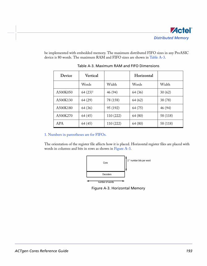
Distributed Memory
be implemented with embedded memory. The maximum distributed FIFO sizes in any ProASIC device is 80 words. The maximum RAM and FIFO sizes are shown in Table A-3.
1. Numbers in parentheses are for FIFOs.
The orientation of the register file affects how it is placed. Horizontal register files are placed with words in columns and bits in rows as shown in Figure A-3.
Figure A-3. Horizontal Memory
Table A-3. Maximum RAM and FIFO Dimensions
Device Vertical Horizontal
Words Width Words Width
A500K050 64 (23)1 46 (94) 64 (36) 30 (62)
A500K130 64 (29) 78 (158) 64 (62) 38 (78)
A500K180 64 (36) 95 (192) 64 (75) 46 (94)
A500K270 64 (45) 110 (222) 64 (80) 58 (118)
APA 64 (45) 110 (222) 64 (80) 58 (118)
Decoders
Core2 * number bits per word
number of words
ACTgen Cores Reference Guide 193

Vertical memories are placed with bits in columns and words in rows as shown inFigure A-4.
Figure A-4. Vertical Memory
The decoder sizes are given in table Table A-4.
Calculating Logic UsageThe following section presents how to calculate logic usage for Memory area, and a vertical and a horizontal memory.
Memory Area
The following is an example of how to calculate memory area:
Memory Area = Number of Words (2 * Number of bits +decoder size)
Table A-4. Decoder Sizes
Number of Words Decoder Size
2 ~ 4 1
5 ~ 8 2
9 ~ 64 3
Dec
oder
s
Cor
e
2 * number bits per word
num
ber
ofw
ords
194 ACTgen Cores Reference Guide

Distributed Memory
Vertical Orientation
The following is an example logic usage calculation for a 16x32 RAM:
Width in tiles = 2 * number-of-Bits-per-word + decoder size
= 2 * 32 + 3 = 67
Height in tiles = number-of-words = 16
Horizontal Orientation
The following is a an example logic usage calculation for a 16x32 RAM:
Tiles in Width = Number-of-Words = 16
Tiles in Height = 2 * number-of-bits-per-word + decoder size
= 2 * 32 + 3 = 67
ACTgen displays the legal coordinates to place the memory if the core is not rotated or flipped. The horizontal could be placed between the coordinates (1,1) and (145, 15) assuming the A500K130 device was selected.
Distributed Memory Placement
To achieve the best timing and efficient placement, use the placement constraints file generated by ACTgen. For more information on constraint statements, refer to the Actel Quick Start Guide. To utilize this file, use the “set_location” constraint statement for cores. For example:
set_location (x,y) <mem_hier_name> <macro_name>;
Distributed Memory Timing
Memory timing values are dependent on the memory size and the routing to and from the memory. Since the memories are implemented as ProASIC primitives, users can determine the timing characteristics of the circuit by performing a back annotated timing analysis. In fact, to the timing analyzer, the distributed memory looks like any other part of the circuit and requires no special treatment. “Timing for Distrubuted Memories” on page 196 explains the critical timing paths in each memory, and why these paths are critical.
ACTgen Cores Reference Guide 195
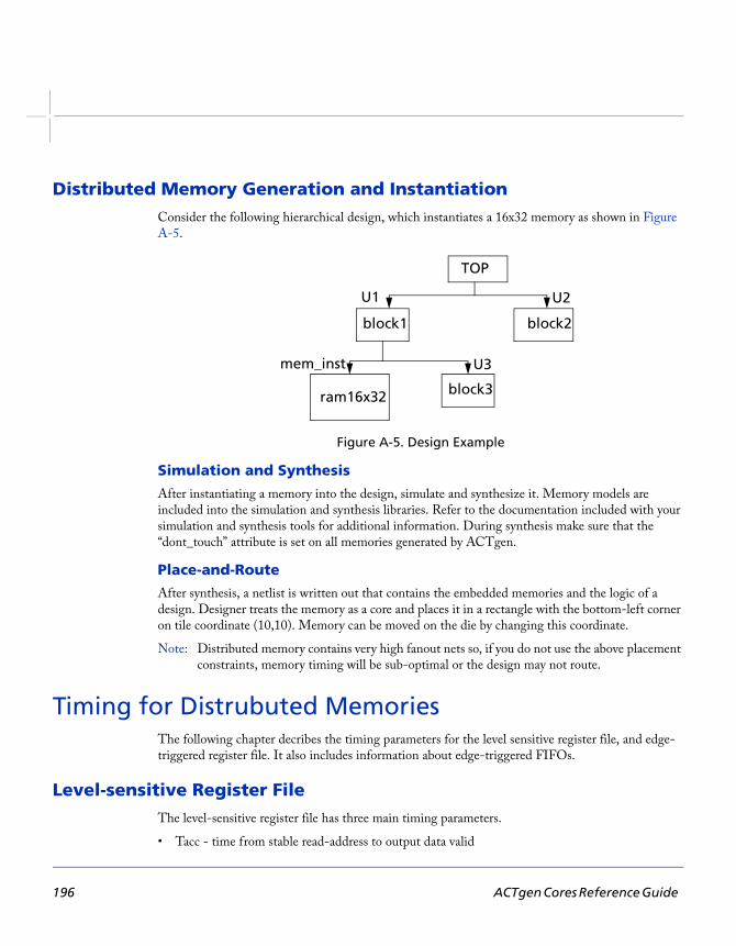
Distributed Memory Generation and InstantiationConsider the following hierarchical design, which instantiates a 16x32 memory as shown in Figure A-5.
Figure A-5. Design Example
Simulation and Synthesis
After instantiating a memory into the design, simulate and synthesize it. Memory models are included into the simulation and synthesis libraries. Refer to the documentation included with your simulation and synthesis tools for additional information. During synthesis make sure that the “dont_touch” attribute is set on all memories generated by ACTgen.
Place-and-Route
After synthesis, a netlist is written out that contains the embedded memories and the logic of a design. Designer treats the memory as a core and places it in a rectangle with the bottom-left corner on tile coordinate (10,10). Memory can be moved on the die by changing this coordinate.
Note: Distributed memory contains very high fanout nets so, if you do not use the above placement constraints, memory timing will be sub-optimal or the design may not route.
Timing for Distrubuted MemoriesThe following chapter decribes the timing parameters for the level sensitive register file, and edge-triggered register file. It also includes information about edge-triggered FIFOs.
Level-sensitive Register FileThe level-sensitive register file has three main timing parameters.
• Tacc - time from stable read-address to output data valid
TOP
block1 block2
ram16x32 block3
U1 U2
U3mem_inst
196 ACTgen Cores Reference Guide

Timing for Distrubuted Memories
• Tsetup_data - time from stable write-data to falling edge of WR
• Tsetup_addr - time from stable write-address to rising clock edge
Figure A-6 shows the timing of these parameters:
Figure A-6. Level-sensitive Mode Timing Diagram
Failure to meet these timing values will have the following results:
• Tacc - read data might be from previous address
• Tsetup_data - data may not be written into the memory
• Tsetup_addr - data may be written into some other address as well as the intended address
Edge-triggered Register File The edge-triggered register file has three main timing parameters:
• Tacc - time from stable read-address to output data valid
• Tsetup_data - time from stable write-data to rising WR edge
• Tsetup_addr - time from stable write-address to rising WR edge
rAddr
rData
wData
wAddr
WR
Tacc
Tsetup_data
Tsetup_addr
ACTgen Cores Reference Guide 197

Figure A-7 shows the relationships of the signals.
Figure A-7. Edge-triggered Mode Timing Diagram
Failure to meet these timing values will have the following results:
• Tacc read data might be from previous address
• Tsetup_data data may not be written into the memory
• Tsetup_addr data may be written into some other address
The main advantage of the edge-triggered memory is that the write timing is sensitive only to the rising edge of the WR, not both the rising and falling edges.
Edge-Triggered FIFO The edge-triggered FIFO captures data on the rising edge of the “WR” signal, and the read pointers advance on the rising edge of the “RD” signal. Before using the FIFO, it must be initialized by pulsing the “INIT” signal high. Immediately after initialization, the “empty” signal is true and the “full” signal false. Data applied on the “wDataX” signals are captured when the “WR” signal transitions from 0 to 1. Simultaneously, the “empty” signal will become false to indicate that there is valid data on “rDataX.” Further transitions from 0 to 1 on “WR” captures more data into the FIFO until such time as “full” becomes true. At this point, the FIFO is full, and no more data should be entered into it.
After the FIFO is initialized, the output data remains invalid until the first read operation is performed. With every rising edge of the read pulse, the FIFO generates the next word written into it on the output data bus until all the words written into it are read out. At this point the “empty” signal goes high. Further read operations produce no change to the data output as it remains fixed at the last word written into the FIFO.
rAddr
rDataTacc
wData
wAddr
WR
Tsetup_data
Tsetup_addr
198 ACTgen Cores Reference Guide

Using Multiple Memories in a Design
Figure A-8 shows an example of an Edge triggered FIFO. It has the following main timing:
• Tacc - Access from RD rising edge to output data valid
• Tacc - Access from RD rising edge to output data valid
• Tsu - Setup time from stable write-data to rising WR edge
• Thold - Hold time for write-data from rising WR edge
Figure A-8. Edge-triggered FIFO Timing Diagram
Level Sensitive FIFOThe level sensitive FIFO has the same timing as the edge-triggered FIFO. The only difference is that the data input is latched at the falling edge of the write pulse.
Using Multiple Memories in a DesignThis chapter describes how to use multiple memories in a design. If a design includes several memories with different sizes and access modes, Actel recommends generating them all in one session of ACTgen. The embedded memories are automatically generated and are accompanied by placement directives.
Multiple Memory Generation and IntegrationProASIC devices contain dedicated embedded memory blocks that can be configured as RAM or FIFO. Multiple memory blocks can be combined together to create deep and wide memories. ACTgen does this by combining multiple memory blocks as required. The tool generates netlists for
Tacc
rData
RD
wData
WRTsu Thold
ACTgen Cores Reference Guide 199

these blocks. Netlist instantiates memory leaf cells. Consider the following design shown in Figure A-9.
Figure A-9. Sample Design
In this design, there is a receive FIFO and transmit FIFO. Read and Write ports are synchronous. Each FIFO is 32 words deep and 64 bits wide. Also, both FIFOs are identical. Only one FIFO needs to be created with ACTgen, and it must be instantiated twice into the design.
Once the FIFO is generated with ACTgen, it must be instantiated into the design. The following is an example of the RTL after instantiation:
module top(tran_data, rec_data, rec_data_valid,tran_data_valid, clk, reset, rec_fifo_full,rec_fifo_empty, tran_fifo_full, tran_fifo_empty);// this is top level module
input rec_data_valid, clk, reset, tran_data_valid;output[63:0] tran_data;output rec_fifo_full, rec_fifo_empty,tran_fifo_full, tran_fifo_empty;input[63:0] rec_data;wire[63:0] data_int;/* Receiver FIFO instantiation */ sync_fifo rec_FI(.data_in(rec_data),.data_out(data_int),
.wr(rec_data_valid), .rd(1'b0),
.empty(rec_fifo_empty), .full(rec_fifo_full),
.reset(reset), .clk(clk));/* transmit FIFO instantiation */sync_fifo tran_FI(.data_in(data_int),
.data_out (tran_fifo_full)
.wr(1'b0), .rd(tran_data_valid),
.empty(tran_fifo_empty), .full(tran_fifo_full),
.reset(reset), .clk(clk));/* other RTL of the design and other blocks */
Receive FIFO32x64
Transmit FIFO32x64
Rec data64
64
CLK
Rec data valid
Int data
64
Tran data valid
Transmit data
Tran FIFO emptyTran FIFO fullRec FIFO full Rec FIFO empty
200 ACTgen Cores Reference Guide

Using Multiple Memories in a Design
endmodule
module sync_fifo (data_in, data_out, wr, rd, empty, full, reset, clk);input[63:0] data_in;output[63:0] data_out;input wr, rd,clk, reset;output empty, full;/* Instantiation of FIFO generated from ACTgen */fifo32x64 F1(.DO(data_out), .RCLOCK(clk), .WCLOCK(clk),
.DI(data_in), .WRB(wr), .RDB(rd), .RESET(reset),
.FULL(full), .EMPTY(empty), .EQTH(), .GEQTH());
endmodule
Simulate and Synthesize
Now the design can be simulated and synthesized. The following is an example of a Verilog-XL simulation command:
verilog test_sim.v top.v fifo32x64.v –v $AMHOME/etc/deskits/verilog/lib/A500K.v
The following is a typical Design Compiler script for synthesis of a design including memory blocks:
read –format verilog fifo32x64set_dont_touch find(design, “fifo32x64”) /* memories must be dont_touch during synthesis */ read –format verilog top.vcreate_clock –period 20 clk /* add timing constraints */set_wire_load A500Kset_operating_conditions WORSTcompileset_port_is_pad “*” /* use set_pad_type to to use a particular type of pad */insert_padswrite –format verilog –hierarchy –output top_str.v /* write out netlist with hierarchy */quit
Memory Placement
The netlist “top_str.v”contains both FIFO instantiations and can be used for post synthesis gate level simulation. After synthesis, you can place and route the design. In this example, each FIFO uses 8 memory blocks. Designer automatically attempts to place each FIFO in a line. The resulting placement on an A500K130 device, which has 20 memory slots, is shown in Figure A-10 on page
ACTgen Cores Reference Guide 201

202. For information about the ChipEdit tool, refer to the ChipEdit User’s Guide or the ChipEdit online help.
Figure A-10. Sample Memory Placement (Screen May Vary Slightly)
During placement Designer attempts to keep one memory entity in one group. In the example shown in Figure A-10, it placed the “Rec_FI/F1/M0” in the first memory slot on the left side of the lower row, and “rec_FI/F1/M1” in next slot and so on. Only ten slots were available in one row and therefore, the placement of “tran_FI” started from the upper row. If each memory block had used four blocks, both memory blocks would be placed one after another in the lower row.
Manual Placement of Multiple MemoriesA memory placement file must be created to manually place memories. For example, to place the “rec_FI” from the previous example on the left side using both rows and the “tran_FI” on right side in both rows, the following placement file would be used:
set_location (1,81) rec_FI/F1/M0;set_location (1,89) rec_FI/F1/M1;set_location (17,89) rec_FI/F1/M2;set_location (17,81) rec_FI/F1/M3;set_location (33,81) rec_FI/F1/M4;set_location (33,89) rec_FI/F1/M5;set_location (49,89) rec_FI/F1/M6;
M7M4M6M7 M2
M5M3
M3M1 M4M2M0M1 M0M5
M6
8 blocks of tran_FI
8 blocks of Rec_FI
202 ACTgen Cores Reference Guide

Using Multiple Memories in a Design
set_location (49,81) rec_FI/F1/M7;
set_location (145,81) tran_FI/F1/M0;set_location (145,89) tran_FI/F1/M1;set_location (129,89) tran_FI/F1/M2;set_location (129,81) tran_FI/F1/M3;set_location (113,81) tran_FI/F1/M4;set_location (113,89) tran_FI/F1/M5;set_location (97,89) tran_FI/F1/M6;set_location (97,81) tran_FI/F1/M7;
This constraints file should be read into Designer and would result in the placement shown in Figure A-11 on an A500K130 device.
Figure A-11. Sample FIFO Placement
Designer determines the placement for each memory and keeps each memory entity together. To change default placement, you can create constraints manually for memory placement as described in Chapter 1.
Glue Logic for Wider or Deeper Memories
If very deep or very wide memories are created, ACTgen combines together multiple basic blocks and uses embedded logic. Two lists quantifying glue logic are shown in Table A-5 and Table A-6 on page 204 .
These tables cover extreme cases of depth or width for RAMs and FIFOs for the A500K130 device, which offers 20 memory blocks and 12800 logic tiles.
Table A-5. RAM
RAM ParityMemory
Blocks UsedLogic Tile
UsedComment
Depth 5120 Width 8
Check Even 20 259All 20 blocks used in depth
M1 M6M5M2 M1M2M5M6
M0 M7M4M3 M0M3M4M7
Tran FIFORec FIFO
ACTgen Cores Reference Guide 203

For FIFOs, ACTgen creates placement directives for glue logic. If placement information from ACTgen is used, glue logic placement is more efficient.
Programmable Flags in FIFOsProASIC devices provide programmable flags for FIFOs. The threshold for these flags can be set in ACTgen in the main menu. It is on the bottom right corner in the FIFO Trigger Level box. You can specify whether the flag is static or dynamic. If dynamic is selected, ACTgen will create a FIFO with a LEVEL input bus on the memory interface. You can apply values in the range of 0 to 255 to this bus to change its threshold dynamically.
The overall trigger level is a multiple “d,” which is the number of used basic memory blocks in depth (each 256 words). The increment between each overall trigger level is equal to “d.” For example, a memory that is 512 words deep is built up of two basic memory block in depth (512/256). The highest almost full trigger level should be assigned, which is 510 (512-d = 512-2) The corresponding dynamic trigger LEVEL is 255 (510/n = 510/2).
If the threshold is not changing, you can select the static option and specify the threshold value. In this case, ACTgen will hardwire threshold to the specified value. A detailed timing of these flags can be found in the ProASIC 500k Family Datasheet.
Depth 256 Width 160
Check Even 20 22All 20 blocks used in width
Table A-6. FIFO
FIFO ParityMemory Blocks
UsedLogic Tile
UsedComment
Depth 5120 Width 8
Check Even 20 592All 20 blocks used in depth
Depth 256 Width 160
Check Even 20 62All 20 blocks used in width
Table A-5. RAM
RAM ParityMemory
Blocks UsedLogic Tile
UsedComment
204 ACTgen Cores Reference Guide

Using Multiple Memories in a Design
Trigger level is also called threshold. Consequently, equal threshold (EQTH) and greater equal threshold (GEQTH) are the names of the trigger flags.
ACTgen Cores Reference Guide 205

206 ACTgen Cores Reference Guide

BProduct Support
Actel backs its products with various support services including Customer Service, a Customer Technical Support Center, a web site, an FTP site, electronic mail, and worldwide sales offices. This appendix contains information about contacting Actel and using these support services.
Customer ServiceContact Customer Service for non-technical product support, such as product pricing, product upgrades, update information, order status, and authorization.
From Northeast and North Central U.S.A., call 650.318.4480From Southeast and Southwest U.S.A., call 650. 318.4480From South Central U.S.A., call 650.318.4434From Northwest U.S.A., call 650.318.4434From Canada, call 650.318.4480From Europe, call 650.318.4252 or +44 (0) 1276 401 500From Japan, call 650.318.4743From the rest of the world, call 650.318.4743Fax, from anywhere in the world 650. 318.8044
Actel Customer Technical Support CenterActel staffs its Customer Technical Support Center with highly skilled engineers who can help answer your hardware, software, and design questions. The Customer Technical Support Center spends a great deal of time creating application notes and answers to FAQs. So, before you contact us, please visit our online resources. It is very likely we have already answered your questions.
Actel Technical SupportVisit the Actel Customer Support website (www.actelcom/.custsup/search.html) for more information and support. Many answers available on the searchable web resource include diagrams, illustrations, and links to other resources on the Actel web site.
WebsiteYou can browse a variety of technical and non-technical information on Actel’s home page, at www.actel.com.
ACTgen Cores Reference Guide 207

Contacting the Customer Technical Support CenterHighly skilled engineers staff the Technical Support Center from 7:00 A.M. to 6:00 P.M., Pacific Time, Monday through Friday. Several ways of contacting the Center follow:
EmailYou can communicate your technical questions to our email address and receive answers back by email, fax, or phone. Also, if you have design problems, you can email your design files to receive assistance. We constantly monitor the email account throughout the day. When sending your request to us, please be sure to include your full name, company name, and your contact information for efficient processing of your request.
The technical support email address is [email protected].
PhoneOur Technical Support Center answers all calls. The center retrieves information, such as your name, company name, phone number and your question, and then issues a case number. The Center then forwards the information to a queue where the first available application engineer receives the data and returns your call. The phone hours are from 7:00 A.M. to 6:00 P.M., Pacific Time, Monday through Friday. The Technical Support numbers are:
650.318.4460800.262.1060
Customers needing assistance outside the US time zones can either contact technical support via email ([email protected]) or contact a local sales office. Sales office listings can be found at www.actel.com/contact/offices/index.html.
208 ACTgen Cores Reference Guide