ACT 2 Family FPGAs datasheet - Digi-Key Sheets/Microsemi PDFs/Act2... · ACT 2 Family FPGAs...
54
January 2012 I © 2012 Microsemi Corporation ACT 2 Family FPGAs Features • Up to 8,000 Gate Array Gates (20,000 PLD equivalent gates) • Replaces up to 200 TTL Packages • Replaces up to eighty 20-Pin PAL ® Packages • Design Library with over 500 Macro Functions • Single-Module Sequence Functions • Wide-Input Combinatorial Functions • Up to 1,232 Programmable Logic Modules • Up to 998 Flip-Flops • Datapath Performance at 105 MHz • 16-Bit Accumulator Performance to 39 MHz • Two In-Circuit Diagnostic Probe Pins Support Speed Analysis to 50 MHz • Two High-Speed, Low-Skew Clock Networks • I/O Drive to 10 mA • Nonvolatile, User Programmable • Logic Fully Tested Prior to Shipment • 1.0 micron CMOS Technology Table 1 • ACT 2 Product Family Profile Device A1225A A1240A A1280A Capacity Gate Array Equivalent Gates 2,500 4,000 8,000 PLD Equivalent Gates 6,250 10,000 20,000 TTL Equivalent Package 63 100 200 20-Pin PAL Equivalent Packages 25 40 80 Logic Modules 451 684 1,232 S-Module 231 348 624 C-Module 220 336 608 Flip-Flops (maximum) 382 568 998 Routing Resources Horizontal Tracks/Channel 36 36 36 Vertical Tracks/Channel 15 15 15 PLICE Antifuse Elements 250,000 400,000 750,000 User I/Os (maximum) 83 104 140 Performance 1 16-Bit Prescaled Counters 105 MHz 100 MHz 85 MHz 16-Bit Loadable Counters 70 MHz 69 MHz 67 MHz 16-Bit Accumulators 39 MHz 38 MHz 36 MHz Packages 2 CPGA PLCC PQFP VQFP TQFP CQFP PG100 PL84 PQ100 VQ100 – – PG132 PL84 PQ144 – TQ176 – PG176 PL84 PQ160 – TQ176 CQ172 Notes: 1. Performance is based on –2 speed devices at commercial worst-case operating conditions using PREP Benchmarks, Suite #1, Version 1.2, dated 3-28-93. Any analysis is not endorsed by PREP. 2. See the "Product Plan" on page III for package availability. Revision 8
Transcript of ACT 2 Family FPGAs datasheet - Digi-Key Sheets/Microsemi PDFs/Act2... · ACT 2 Family FPGAs...

Revision 8
ACT 2 Family FPGAsFeatures
• Up to 8,000 Gate Array Gates (20,000 PLD equivalent gates)
• Replaces up to 200 TTL Packages• Replaces up to eighty 20-Pin PAL® Packages• Design Library with over 500 Macro Functions• Single-Module Sequence Functions• Wide-Input Combinatorial Functions• Up to 1,232 Programmable Logic Modules• Up to 998 Flip-Flops
• Datapath Performance at 105 MHz• 16-Bit Accumulator Performance to 39 MHz• Two In-Circuit Diagnostic Probe Pins Support Speed
Analysis to 50 MHz• Two High-Speed, Low-Skew Clock Networks• I/O Drive to 10 mA• Nonvolatile, User Programmable• Logic Fully Tested Prior to Shipment• 1.0 micron CMOS Technology
Table 1 • ACT 2 Product Family ProfileDevice A1225A A1240A A1280ACapacity
Gate Array Equivalent Gates 2,500 4,000 8,000PLD Equivalent Gates 6,250 10,000 20,000TTL Equivalent Package 63 100 20020-Pin PAL Equivalent Packages 25 40 80
Logic Modules 451 684 1,232S-Module 231 348 624C-Module 220 336 608
Flip-Flops (maximum) 382 568 998Routing Resources
Horizontal Tracks/Channel 36 36 36Vertical Tracks/Channel 15 15 15PLICE Antifuse Elements 250,000 400,000 750,000
User I/Os (maximum) 83 104 140Performance1
16-Bit Prescaled Counters 105 MHz 100 MHz 85 MHz16-Bit Loadable Counters 70 MHz 69 MHz 67 MHz16-Bit Accumulators 39 MHz 38 MHz 36 MHz
Packages2 CPGAPLCCPQFPVQFPTQFPCQFP
PG100PL84
PQ100VQ100
––
PG132PL84
PQ144–
TQ176–
PG176PL84
PQ160–
TQ176CQ172
Notes:1. Performance is based on –2 speed devices at commercial worst-case operating conditions using PREP Benchmarks, Suite #1,
Version 1.2, dated 3-28-93. Any analysis is not endorsed by PREP.2. See the "Product Plan" on page III for package availability.
January 2012 I© 2012 Microsemi Corporation
ACT 2 Family FPGAs
Ordering Information
_
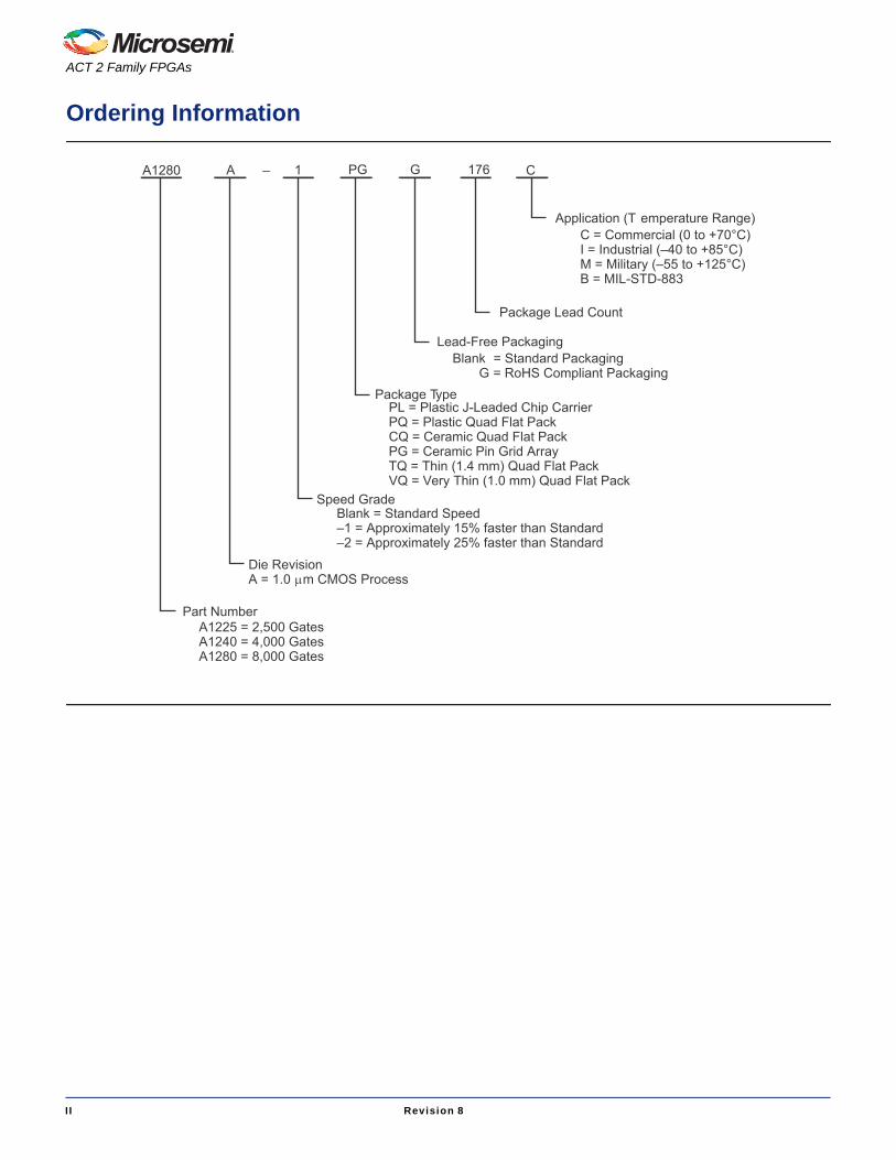
Part Number
Speed Grade
Package Type
Package Lead Count
C = Commercial (0 to +70°C)I = Industrial (–40 to +85°C)M = Military (–55 to +125°C)B = MIL-STD-883
Application (T emperature Range)
PL = Plastic J-Leaded Chip CarrierPQ = Plastic Quad Flat PackCQ = Ceramic Quad Flat PackPG = Ceramic Pin Grid ArrayTQ = Thin (1.4 mm) Quad Flat PackVQ = Very Thin (1.0 mm) Quad Flat Pack
Blank = Standard Speed–1 = Approximately 15% faster than Standard–2 = Approximately 25% faster than Standard
A1225 = 2,500 GatesA1240 = 4,000 GatesA1280 = 8,000 Gates
A1280 1
Die RevisionA = 1.0 μm CMOS Process
A PG 176G C
Lead-Free PackagingBlank = Standard Packaging
G = RoHS Compliant Packaging
I I Revision 8

ACT 2 Family FPGAs
Product Plan
Device Resources
Contact your local Microsemi SoC Products Group representative for device availability:http://www.microsemi.com/soc/contact/default.aspx.
Device/Package
Speed Grade1 Application1
Std. –1 –2 C I M B
A1225A Device
84-Pin Plastic Leaded Chip Carrier (PL) ✓ ✓ ✓ ✓ ✓ – –
100-Pin Plastic Quad Flatpack (PQ) ✓ ✓ ✓ ✓ ✓ – –
100-Pin Very Thin Quad Flatpack (VQ) ✓ ✓ ✓ ✓ – – –
100-Pin Ceramic Pin Grid Array (PG) ✓ ✓ ✓ ✓ – – –
A1240A Device
84-Pin Plastic Leaded Chip Carrier (PL) ✓ ✓ ✓ ✓ ✓ – –
132-Pin Ceramic Pin Grid Array (PG) ✓ ✓ ✓ ✓ – ✓ ✓
144-Pin Plastic Quad Flat Pack (PQ) ✓ ✓ ✓ ✓ ✓ – –
176-Pin Thin (1.4 mm) Quad Flat Pack (TQ) ✓ ✓ ✓ ✓ – – –
A1280A Device
160-Pin Plastic Quad Flatpack (PQ) ✓ ✓ ✓ ✓ ✓ – –
172-Pin Ceramic Quad Flatpack (CQ) ✓ ✓ ✓ ✓ – ✓ ✓
176-Pin Ceramic Pin Grid Array (PG) ✓ ✓ ✓ ✓ – ✓ ✓
176-Pin Thin (1.4 mm) Quad Flat Pack (TQ) ✓ ✓ ✓ ✓ – – –
Notes:1. Applications:
C = CommercialI = IndustrialM = MilitaryB = MIL-STD-883
Availability:✓ = AvailableP = Planned– = Not planned
Speed Grade:–1 = Approx. 15% faster than Std.–2 = Approx. 25% faster than Std.
2. Contact your Microsemi SoC Products Group sales representative for product availability.
Device Series
Logic Modules Gates
User I/Os
PG176 PG132 PG100 PQ160 PQ144 PQ100 PL84 CQ172 TQ176 VQ100
A1225A 451 2,500 – – 83 – – 83 72 – – 83
A1240A 684 4,000 – 104 – – 104 – 72 – 104 –
A1280A 1,232 8,000 140 – – 125 – – 72 140 140 –
Revision 8 III

ACT 2 Family FPGAs
Revision 8 IV
Table of Contents
ACT 2 Family OverviewGeneral Description . . . . . . . . . . . . . . . . . . . . . . . . . . . . . . . . . . . . . . . . . . . . . . . . . . . . . . . . . . . . . . . . . . . . . . . . . . 1-1
Detailed SpecificationsOperating Conditions . . . . . . . . . . . . . . . . . . . . . . . . . . . . . . . . . . . . . . . . . . . . . . . . . . . . . . . . . . . . . . . . . . . . 2-1Package Thermal Characteristics . . . . . . . . . . . . . . . . . . . . . . . . . . . . . . . . . . . . . . . . . . . . . . . . . . . . . . . . . . . . . . . 2-3Power Dissipation . . . . . . . . . . . . . . . . . . . . . . . . . . . . . . . . . . . . . . . . . . . . . . . . . . . . . . . . . . . . . . . . . . . . . . . . . . . 2-3ACT 2 Timing Model1 . . . . . . . . . . . . . . . . . . . . . . . . . . . . . . . . . . . . . . . . . . . . . . . . . . . . . . . . . . . . . . . . . . . . . . . 2-7Pin Descriptions . . . . . . . . . . . . . . . . . . . . . . . . . . . . . . . . . . . . . . . . . . . . . . . . . . . . . . . . . . . . . . . . . . . . . . . . . . . . 2-21
Package Pin AssignmentsPL84 . . . . . . . . . . . . . . . . . . . . . . . . . . . . . . . . . . . . . . . . . . . . . . . . . . . . . . . . . . . . . . . . . . . . . . . . . . . . . . . . . . . . . 3-1PQ100 . . . . . . . . . . . . . . . . . . . . . . . . . . . . . . . . . . . . . . . . . . . . . . . . . . . . . . . . . . . . . . . . . . . . . . . . . . . . . . . . . . . . 3-3PQ144 . . . . . . . . . . . . . . . . . . . . . . . . . . . . . . . . . . . . . . . . . . . . . . . . . . . . . . . . . . . . . . . . . . . . . . . . . . . . . . . . . . . . 3-5PQ160 . . . . . . . . . . . . . . . . . . . . . . . . . . . . . . . . . . . . . . . . . . . . . . . . . . . . . . . . . . . . . . . . . . . . . . . . . . . . . . . . . . . . 3-7VQ100 . . . . . . . . . . . . . . . . . . . . . . . . . . . . . . . . . . . . . . . . . . . . . . . . . . . . . . . . . . . . . . . . . . . . . . . . . . . . . . . . . . . . 3-9CQ172 . . . . . . . . . . . . . . . . . . . . . . . . . . . . . . . . . . . . . . . . . . . . . . . . . . . . . . . . . . . . . . . . . . . . . . . . . . . . . . . . . . . 3-14PG100 . . . . . . . . . . . . . . . . . . . . . . . . . . . . . . . . . . . . . . . . . . . . . . . . . . . . . . . . . . . . . . . . . . . . . . . . . . . . . . . . . . . 3-16PG132 . . . . . . . . . . . . . . . . . . . . . . . . . . . . . . . . . . . . . . . . . . . . . . . . . . . . . . . . . . . . . . . . . . . . . . . . . . . . . . . . . . . 3-18PG176 . . . . . . . . . . . . . . . . . . . . . . . . . . . . . . . . . . . . . . . . . . . . . . . . . . . . . . . . . . . . . . . . . . . . . . . . . . . . . . . . . . . 3-20
Datasheet InformationList of Changes . . . . . . . . . . . . . . . . . . . . . . . . . . . . . . . . . . . . . . . . . . . . . . . . . . . . . . . . . . . . . . . . . . . . . . . . . . . . . 4-1Datasheet Categories . . . . . . . . . . . . . . . . . . . . . . . . . . . . . . . . . . . . . . . . . . . . . . . . . . . . . . . . . . . . . . . . . . . . . . . . 4-2Safety Critical, Life Support, and High-Reliability Applications Policy . . . . . . . . . . . . . . . . . . . . . . . . . . . . . . . . . . . . 4-2

1 – ACT 2 Family Overview
General DescriptionThe ACT 2 family represents Actel’s second generation of field programmable gate arrays(FPGAs). The ACT 2 family presents a two-module architecture, consisting of C-modules and S-modules. These modules are optimized for both combinatorial and sequential designs. Based on Actel’spatented channeled array architecture, the ACT 2 family provides significant enhancements to gatedensity and performance while maintaining downward compatibility with the ACT 1 design environmentand upward compatibility with the ACT 3 design environment. The devices are implemented in silicongate, 1.0-μm, two-level metal CMOS, and employ Actel’s PLICE® antifuse technology. This revolutionaryarchitecture offers gate array design flexibility, high performance, and fast time-to-production with userprogramming. The ACT 2 family is supported by the Designer and Designer Advantage Systems, whichoffers automatic pin assignment, validation of electrical and design rules, automatic placement androuting, timing analysis, user programming, and diagnostic probe capabilities. The systems aresupported on the following platforms: 386/486™ PC, Sun™, and HP™ workstations. The systemsprovide CAE interfaces to the following design environments: Cadence, Viewlogic®, Mentor Graphics®,and OrCAD™.
Revision 8 1-1


2 – Detailed Specifications
Operating ConditionsTable 2-1 • Absolute Maximum Ratings1
Symbol Parameter Limits Units
VCC DC supply voltage –0.5 to +7.0 V
VI Input voltage –0.5 to VCC + 0.5 V
VO Output voltage –0.5 to VCC + 0.5 V
IIO I/O source sink current2 ±20 mA
TSTG Storage temperature –65 to +150 °C
Notes:1. Stresses beyond those listed under "Absolute Maximum Ratings" may cause permanent damage to the device.
Exposure to absolute maximum rated conditions for extended periods may affect device reliability. Device should not beoperated outside the recommended operating conditions.
2. Device inputs are normally high impedance and draw extremely low current. However, when input voltage is greaterthan VCC + 0.5 V for less than GND –0.5 V, the internal protection diodes will be forward biased and can drawexcessive current.
Table 2-2 • Recommended Operating Conditions
Parameter Commercial Industrial Military Units
Temperature range* 0 to +70 –40 to +85 –55 to +125 °C
Power supply tolerance ±5 ±10 ±10 %VCC
Note: *Ambient temperature (TA) is used for commercial and industrial; case temperature (TC) is used for military.
Revision 8 2-1

Detailed Specifications
Table 2-3 • Electrical Specifications
Symbol Parameter
Commercial Industrial Military
UnitsMin. Max. Min. Max. Min. Max.
VOH1 (IOH = –10 mA)2 2.4 – – – – – V
(IOH = –6 mA) 3.84 – – – – – V
(IOH = –4 mA) – – 3.7 – 3.7 – V
VOL1 (IOL = 10 mA)2 – 0.5 – – – – V
(IOL = 6 mA) – 0.33 – 0.40 – 0.40 V
VIL –0.3 0.8 –0.3 0.8 –0.3 0.8 V
VIH 2.0 VCC + 0.3 2.0 VCC + 0.3 2.0 VCC + 0.3 V
Input Transition Time tR, tF2 – 500 – 500 – 500 ns
CIO I/O capacitance2,3 – 10 – 10 – 10 pF
Standby Current, ICC4 (typical = 1 mA) – 2 – 10 – 20 mA
Leakage Current5 –10 +10 –10 +10 –10 +10 µA
ICC(D) Dynamic VCC supply current. See the Power Dissipation section.
Notes:1. Only one output tested at a time. VCC = minimum.2. Not tested, for information only.3. Includes worst-case PG176 package capacitance. VOUT = 0 V, f = 1 MHz4. All outputs unloaded. All inputs = VCC or GND, typical ICC = 1 mA. ICC limit includes IPP and ISV during normal
operations.5. VOUT, VIN = VCC or GND.
2-2 Revision 8

ACT 2 Family FPGAs
Package Thermal CharacteristicsThe device junction to case thermal characteristic is θjc, and the junction to ambient air characteristic isθja. The thermal characteristics for θja are shown with two different air flow rates.Maximum junction temperature is 150°C.A sample calculation of the absolute maximum power dissipation allowed for a PQ160 package atcommercial temperature and still air is as follows:
EQ 1
Power DissipationP = [ICC standby + ICCactive] * VCC + IOL * VOL * N + IOH* (VCC – VOH) * M
EQ 2
where:
ICC standby is the current flowing when no inputs or outputs are changing
ICCactive is the current flowing due to CMOS switching.
IOL and IOH are TTL sink/source currents.
VOL and VOH are TTL level output voltages.
N is the number of outputs driving TTL loads to VOL.
M is the number of outputs driving TTL loads to VOH.
An accurate determination of N and M is problematical because their values depend on the family type,design details, and on the system I/O. The power can be divided into two components: static and active.
Table 2-4 • Package Thermal Characteristics
Package Type* Pin Count θjc
θja Still Air
θja300 ft./min. Units
Ceramic Pin Grid Array 100 5 35 17 °C/W
132 5 30 15 °C/W
176 8 23 12 °C/W
Ceramic Quad Flatpack 172 8 25 15 °C/W
Plastic Quad Flatpack1 100 13 48 40 °C/W
144 15 40 32 °C/W
160 15 38 30 °C/W
Plastic Leaded Chip Carrier 84 12 37 28 °C/W
Very Thin Quad Flatpack 100 12 43 35 °C/W
Thin Quad Flatpack 176 15 32 25 °C/W
Notes: (Maximum Power in Still Air)1. Maximum power dissipation values for PQFP packages are 1.9 W (PQ100), 2.3 W (PQ144), and 2.4 W
(PQ160).2. Maximum power dissipation for PLCC packages is 2.7 W.3. Maximum power dissipation for VQFP packages is 2.3 W.4. Maximum power dissipation for TQFP packages is 3.1 W.
Max. junction temp. (°C) Max. ambient temp. (°C)–θja°C/W
--------------------------------------------------------------------------------------------------------------------------------------- 150°C 70°C–33°C/W
------------------------------------ 2.4 W= =
Revision 8 2-3
Detailed Specifications
Static Power ComponentMicrosemi FPGAs have small static power components that result in lower power dissipation than PALsor PLDs. By integrating multiple PALs/PLDs into one FPGA, an even greater reduction in board-levelpower dissipation can be achieved.The power due to standby current is typically a small component of the overall power. Standby power iscalculated in Table 2-5 for commercial, worst case conditions.
The static power dissipated by TTL loads depends on the number of outputs driving high or low and theDC load current. Again, this value is typically small. For instance, a 32-bit bus sinking 4 mA at 0.33 V willgenerate 42 mW with all outputs driving low, and 140 mW with all outputs driving high. The actualdissipation will average somewhere between as I/Os switch states with time.
Active Power ComponentPower dissipation in CMOS devices is usually dominated by the active (dynamic) power dissipation. Thiscomponent is frequency dependent, a function of the logic and the external I/O. Active power dissipationresults from charging internal chip capacitances of the interconnect, unprogrammed antifuses, moduleinputs, and module outputs, plus external capacitance due to PC board traces and load device inputs.An additional component of the active power dissipation is the totem-pole current in CMOS transistorpairs. The net effect can be associated with an equivalent capacitance that can be combined withfrequency and voltage to represent active power dissipation.
Equivalent CapacitanceThe power dissipated by a CMOS circuit can be expressed by EQ 3.
Power (µW) = CEQ * VCC2 * F
EQ 3
Where:
CEQ is the equivalent capacitance expressed in pF.
VCC is the power supply in volts.
F is the switching frequency in MHz.
Equivalent capacitance is calculated by measuring ICC active at a specified frequency and voltage foreach circuit component of interest. Measurements have been made over a range of frequencies at afixed value of VCC. Equivalent capacitance is frequency independent so that the results may be usedover a wide range of operating conditions. Equivalent capacitance values are shown in Table 2-6.
Table 2-5 • Standby Power Calculation
ICC VCC Power
2 mA 5.25 V 10.5 mW
Table 2-6 • CEQ Values for Microsemi FPGAs
Item CEQ Value
Modules (CEQM) 5.8
Input Buffers (CEQI) 12.9
Output Buffers (CEQO) 23.8
Routed Array Clock Buffer Loads (CEQCR) 3.9
2-4 Revision 8
ACT 2 Family FPGAs
To calculate the active power dissipated from the complete design, the switching frequency of each partof the logic must be known. EQ 4 shows a piece-wise linear summation over all components.
Power =VCC2 * [(m * CEQM * fm)modules + (n * CEQI * fn) inputs
+ (p * (CEQO+ CL) * fp)outputs
+ 0.5 * (q1 * CEQCR * fq1)routed_Clk1 + (r1 * fq1)routed_Clk1
+ 0.5 * (q2 * CEQCR * fq2)routed_Clk2 + (r2 * fq2)routed_Clk2
EQ 4Where:m = Number of logic modules switching at fmn = Number of input buffers switching at fnp = Number of output buffers switching at fpq1 = Number of clock loads on the first routed array clockq2 = Number of clock loads on the second routed array clockr1 = Fixed capacitance due to first routed array clockr2 = Fixed capacitance due to second routed array clockCEQM = Equivalent capacitance of logic modules in pFCEQI = Equivalent capacitance of input buffers in pFCEQO = Equivalent capacitance of output buffers in pFCEQCR = Equivalent capacitance of routed array clock in pFCL = Output lead capacitance in pFfm = Average logic module switching rate in MHzfn = Average input buffer switching rate in MHzfp = Average output buffer switching rate in MHzfq1 = Average first routed array clock rate in MHzfq2 = Average second routed array clock rate in MHz
Table 2-7 • Fixed Capacitance Values for Microsemi FPGAs
Device Type r1, routed_Clk1 r2, routed_Clk2A1225A 106 106.0A1240A 134 134.2A1280A 168 167.8
Revision 8 2-5

Detailed Specifications
Determining Average Switching FrequencyTo determine the switching frequency for a design, you must have a detailed understanding of the datainput values to the circuit. The following guidelines are meant to represent worst-case scenarios so thatthey can be generally used to predict the upper limits of power dissipation. These guidelines are given inTable 2-8.
Table 2-8 • Guidelines for Predicting Power Dissipation
Data Value
Logic Modules (m) 80% of modules
Inputs switching (n) # inputs/4
Outputs switching (p) # output/4
First routed array clock loads (q1) 40% of sequential modules
Second routed array clock loads (q2) 40% of sequential modules
Load capacitance (CL) 35 pF
Average logic module switching rate (fm) F/10
Average input switching rate (fn) F/5
Average output switching rate (fp) F/10
Average first routed array clock rate (fq1) F
Average second routed array clock rate (fq2) F/2
2-6 Revision 8
ACT 2 Family FPGAs
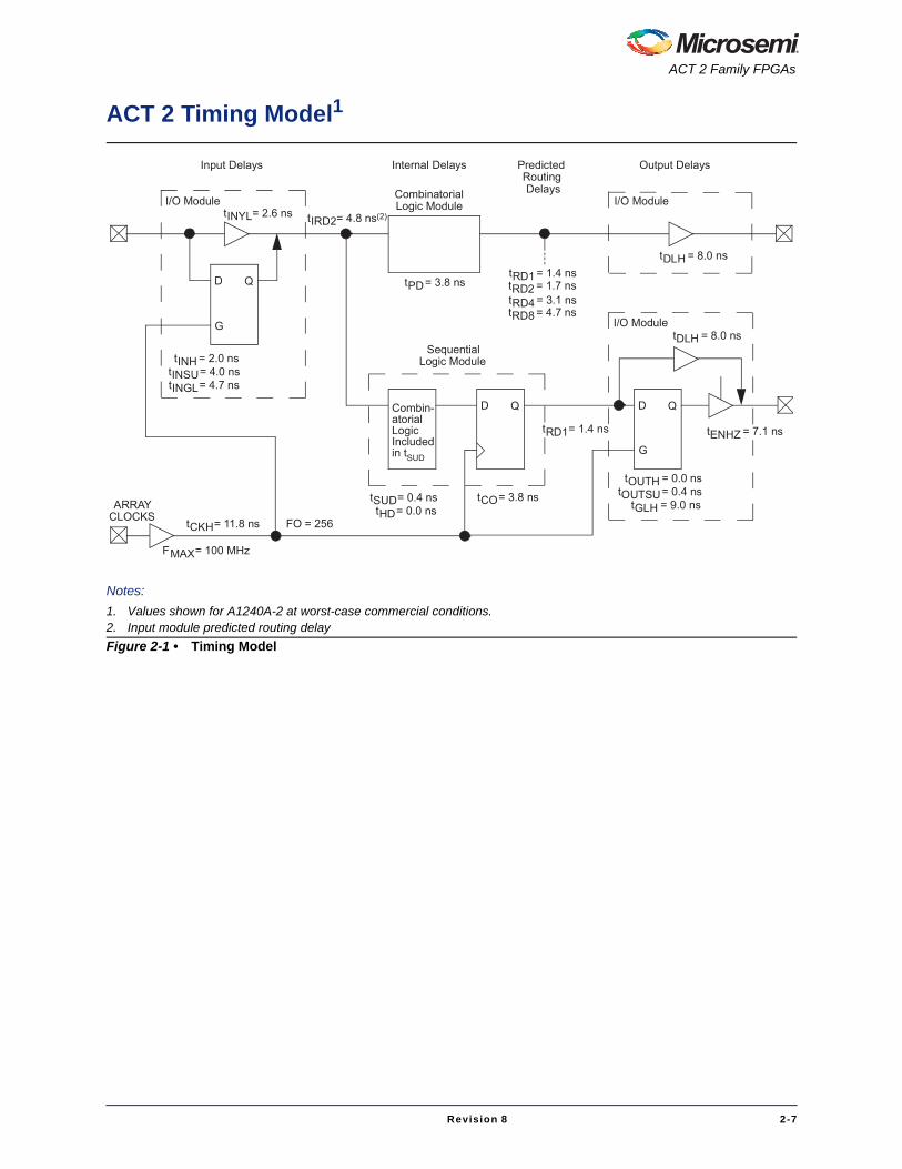
ACT 2 Timing Model1
Notes:1. Values shown for A1240A-2 at worst-case commercial conditions.2. Input module predicted routing delayFigure 2-1 • Timing Model
Output DelaysInternal DelaysInput Delays
tINH = 2.0 nstINSU = 4.0 ns
I/O Module
D Q
tINGL = 4.7 ns
tINYL = 2.6 ns tIRD2 = 4.8 ns(2)
CombinatorialLogic Module
tPD = 3.8 ns
SequentialLogic Module
I/O Module
tRD1 = 1.4 nstDLH = 8.0 ns
I/O Module
ARRAYCLOCKS
FMAX = 100 MHz
Combin-atorialLogicIncludedin tSUD
D Q D Q
tOUTH = 0.0 nstOUTSU = 0.4 ns
tGLH = 9.0 ns
tDLH = 8.0 ns
tENHZ = 7.1 nstRD1 = 1.4 ns
tCO = 3.8 nstSUD = 0.4 nstHD = 0.0 ns
tRD4 = 3.1 nstRD8 = 4.7 ns
PredictedRoutingDelays
tCKH = 11.8 ns
G
G
FO = 256
tRD2 = 1.7 ns
Revision 8 2-7

Detailed Specifications
Parameter Measurement
Figure 2-2 • Output Buffer Delays
Figure 2-3 • AC Test Loads
Figure 2-4 • Input Buffer Delays
To AC test loads (shown below)PADD
E
TRIBUFF
InVCC
GND50%
PADVOL
VOH
1.5 V
tDHS,
50%
1.5 V
tDHS
EVCC
GND50%
PADVOL
1.5 V
tENZL
50%
10%
tENLZ
EVCC
GND50%
PADGND
VOH
1.5 V
tENZH
50%
90%
tENHZ
VCC
Load 1(Used to measure propagation delay)
Load 2(Used to measure rising/falling edges)
50 pF
To the output under testVCC GND
50 pF
To the output under test
R to VCC for tPLZ / tPZL R to GND for tPHZ / tPZHR = 1 kΩ
PAD YINBUF
PAD3 V
0 V1.5 V
YGND
VCC
50%
tINYH
1.5 V
50%
tINYL
2-8 Revision 8

ACT 2 Family FPGAs
Sequential Module Timing Characteristics
Figure 2-5 • Module Delays
SAB
Y
S, A or B
YGND
VCC
50%
tPLH
Y
GND
GND
VCC50%
50% 50%
VCC
50% 50%tPHL
tPHLtPLH
Note: D represents all data functions involving A, B, and S for multiplexed flip-flops.Figure 2-6 • Flip-Flops and Latches
(Positive edge triggered)
ED
CLK CLR
Y
D*
G, CLK
Q
E
PRE, CLR
tWCLKA
tWASYN
tHD
tSUD tA
tWCLKItSUENA
tCO
tRS
tHENA
Revision 8 2-9

Detailed Specifications
Figure 2-7 • Input Buffer Latches
Figure 2-8 • Output Buffer Latches
G
PAD
PADCLK
DATA
G
CLK
tINH
CLKBUF
tINSU
tSUEXT
tHEXT
IBDLDATA
D
G
tOUTSU
tOUTH
PAD
OBDLHS
D
G
2-10 Revision 8

ACT 2 Family FPGAs
Timing Derating Factor (Temperature and Voltage)Table 2-9 • Timing Derating Factor (Temperature and Voltage)
(Commercial Minimum/Maximum Specification) x Industrial Military
Min. Max. Min. Max.
0.69 1.11 0.67 1.23
Table 2-10 • Timing Derating Factor for Designs at Typical Temperature (TJ = 25°C) and Voltage (5.0 V)
(Commercial Maximum Specification) x 0.85
Table 2-11 • Temperature and Voltage Derating Factors(normalized to Worst-Case Commercial, TJ = 4.75 V, 70°C)
–55 –40 0 25 70 85 125
4.50 0.75 0.79 0.86 0.92 1.06 1.11 1.23
4.75 0.71 0.75 0.82 0.87 1.00 1.05 1.13
5.00 0.69 0.72 0.80 0.85 0.97 1.02 1.13
5.25 0.68 0.69 0.77 0.82 0.95 0.98 1.09
5.50 0.67 0.69 0.76 0.81 0.93 0.97 1.08
Note: This derating factor applies to all routing and propagation delays.Figure 2-9 • Junction Temperature and Voltage Derating Curves
(normalized to Worst-Case Commercial, TJ = 4.75 V, 70°C)
0.6
0.7
0.8
0.9
1.0
1.1
1.2
1.3
4.504.755.005.255.50
rotca
F g
nit ar eD
Voltage (V)
125˚C
85˚C70˚C
25˚C
0˚C
–40˚C–55˚C
Revision 8 2-11

Detailed Specifications
A1225A Timing CharacteristicsTable 2-12 • A1225A Worst-Case Commercial Conditions, VCC = 4.75 V, TJ = 70°C
Logic Module Propagation Delays1 –2 Speed3 –1 Speed Std. Speed Units
Parameter/Description Min. Max. Min. Max. Min. Max.
tPD1 Single Module 3.8 4.3 5.0 ns
tCO Sequential Clock to Q 3.8 4.3 5.0 ns
tGO Latch G to Q 3.8 4.3 5.0 ns
tRS Flip-Flop (Latch) Reset to Q 3.8 4.3 5.0 ns
Predicted Routing Delays2
tRD1 FO = 1 Routing Delay 1.1 1.2 1.4 ns
tRD2 FO = 2 Routing Delay 1.7 1.9 2.2 ns
tRD3 FO = 3 Routing Delay 2.3 2.6 3.0 ns
tRD4 FO = 4 Routing Delay 2.8 3.1 3.7 ns
tRD8 FO = 8 Routing Delay 4.4 4.9 5.8 ns
Sequential Timing Characteristics3,4
tSUD Flip-Flop (Latch) Data Input Setup 0.4 0.4 0.5 ns
tHD Flip-Flop (Latch) Data Input Hold 0.0 0.0 0.0 ns
tSUENA Flip-Flop (Latch) Enable Setup 0.8 0.9 1.0 ns
tHENA Flip-Flop (Latch) Enable Hold 0.0 0.0 0.0 ns
tWCLKA Flip-Flop (Latch) Clock Active Pulse Width 4.5 5.0 6.0 ns
tWASYN Flip-Flop (Latch) Clock Asynchronous Pulse Width 4.5 5.0 6.0 ns
tA Flip-Flop Clock Input Period 9.4 11.0 13.0 ns
tINH Input Buffer Latch Hold 0.0 0.0 0.0 ns
tINSU Input Buffer Latch Setup 0.4 0.4 0.5 ns
tOUTH Output Buffer Latch Hold 0.0 0.0 0.0 ns
tOUTSU Output Buffer Latch Setup 0.4 0.4 0.5 ns
fMAX Flip-Flop (Latch) Clock Frequency 105.0 90.0 75.0 MHz
Notes:1. For dual-module macros, use tPD1 + tRD1 + tPDn, tCO + tRD1 + tPDn, or tPD1 + tRD1 + tSUD—whichever is appropriate.2. Routing delays are for typical designs across worst-case operating conditions. These parameters should be used for
estimating device performance. Post-route timing analysis or simulation is required to determine actual worst-caseperformance. Post-route timing is based on actual routing delay measurements performed on the device prior toshipment.
3. Data applies to macros based on the S-module. Timing parameters for sequential macros constructed from C-modulescan be obtained from the DirectTime Analyzer utility.
4. Setup and hold timing parameters for the Input Buffer Latch are defined with respect to the PAD and the D input. Externalsetup/hold timing parameters must account for delay from an external PAD signal to the G inputs. Delay from an externalPAD signal to the G input subtracts (adds) to the internal setup (hold) time.
2-12 Revision 8

ACT 2 Family FPGAs
A1225A Timing Characteristics (continued) Table 2-13 • A1225A Worst-Case Commercial Conditions, VCC = 4.75 V, TJ = 70°C
I/O Module Input Propagation Delays –2 Speed –1 Speed Std. Speed Units
Parameter/Description Min. Max. Min. Max. Min. Max.
tINYH Pad to Y High 2.9 3.3 3.8 ns
tINYL Pad to Y Low 2.6 3.0 3.5 ns
tINGH G to Y High 5.0 5.7 6.6 ns
tINGL G to Y Low 4.7 5.4 6.3 ns
Input Module Predicted Input Routing Delays*
tIRD1 FO = 1 Routing Delay 4.1 4.6 5.4 ns
tIRD2 FO = 2 Routing Delay 4.6 5.2 6.1 ns
tIRD3 FO = 3 Routing Delay 5.3 6.0 7.1 ns
tIRD4 FO = 4 Routing Delay 5.7 6.4 7.6 ns
tIRD8 FO = 8 Routing Delay 7.4 8.3 9.8 ns
Global Clock Network
tCKH Input Low to High FO = 32 10.2 11.0 12.8 ns
FO = 256 11.8 13.0 15.7
tCKL Input High to Low FO = 32 10.2 11.0 12.8 ns
FO = 256 12.0 13.2 15.9
tPWH Minimum Pulse Width High FO = 32 3.4 4.1 4.5 ns
FO = 256 3.8 4.5 5.0
tPWL Minimum Pulse Width Low FO = 32 3.4 4.1 4.5 ns
FO = 256 3.8 4.5 5.0
tCKSW Maximum Skew FO = 32 0.7 0.7 0.7 ns
FO = 256 3.5 3.5 3.5
tSUEXT Input Latch External Setup FO = 32 0.0 0.0 0.0 ns
FO = 256 0.0 0.0 0.0
tHEXT Input Latch External Hold FO = 32 7.0 7.0 7.0 ns
FO = 256 11.2 11.2 11.2
tP Minimum Period FO = 32 7.7 8.3 9.1 ns
FO = 256 8.1 8.8 10.0
fMAX Maximum Frequency FO = 32 130.0 120.0 110.0 ns
FO = 256 125.0 115.0 100.0
Note: *These parameters should be used for estimating device performance. Optimization techniques may furtherreduce delays by 0 to 4 ns. Routing delays are for typical designs across worst-case operating conditions. Post-route timing analysis or simulation is required to determine actual worst-case performance. Post-route timing isbased on actual routing delay measurements performed on the device prior to shipment.
Revision 8 2-13

Detailed Specifications
A1225A Timing Characteristics (continued) Table 2-14 • A1225A Worst-Case Commercial Conditions, VCC = 4.75 V, TJ = 70°C
TTL Output Module Timing1 –2 Speed –1 Speed Std. Speed Units
Parameter/Description Min. Max. Min. Max. Min. Max.
tDLH Data to Pad High 8.0 9.0 10.6 ns
tDHL Data to Pad Low 10.1 11.4 13.4 ns
tENZH Enable Pad Z to High 8.9 10.0 11.8 ns
tENZL Enable Pad Z to Low 11.6 13.2 15.5 ns
tENHZ Enable Pad High to Z 7.1 8.0 9.4 ns
tENLZ Enable Pad Low to Z 8.3 9.5 11.1 ns
tGLH G to Pad High 8.9 10.2 11.9 ns
tGHL G to Pad Low 11.2 12.7 14.9 ns
dTLH Delta Low to High 0.07 0.08 0.09 ns/pF
dTHL Delta High to Low 0.12 0.13 0.16 ns/pF
CMOS Output Module Timing1
tDLH Data to Pad High 10.1 11.5 13.5 ns
tDHL Data to Pad Low 8.4 9.6 11.2 ns
tENZH Enable Pad Z to High 8.9 10.0 11.8 ns
tENZL Enable Pad Z to Low 11.6 13.2 15.5 ns
tENHZ Enable Pad High to Z 7.1 8.0 9.4 ns
tENLZ Enable Pad Low to Z 8.3 9.5 11.1 ns
tGLH G to Pad High 8.9 10.2 11.9 ns
tGHL G to Pad Low 11.2 12.7 14.9 ns
dTLH Delta Low to High 0.12 0.13 0.16 ns/pF
dTHL Delta High to Low 0.09 0.10 0.12 ns/pF
Notes:1. Delays based on 50 pF loading.2. SSO information can be found at www.microsemi.com/soc/techdocs/appnotes/board_consideration.aspx.
2-14 Revision 8

ACT 2 Family FPGAs
A1240A Timing CharacteristicsTable 2-15 • A1240A Worst-Case Commercial Conditions, VCC = 4.75 V, TJ = 70°C
Logic Module Propagation Delays1 –2 Speed3 –1 Speed Std. Speed Units
Parameter/Description Min. Max. Min. Max. Min. Max.
tPD1 Single Module 3.8 4.3 5.0 ns
tCO Sequential Clock to Q 3.8 4.3 5.0 ns
tGO Latch G to Q 3.8 4.3 5.0 ns
tRS Flip-Flop (Latch) Reset to Q 3.8 4.3 5.0 ns
Predicted Routing Delays2
tRD1 FO = 1 Routing Delay 1.4 1.5 1.8 ns
tRD2 FO = 2 Routing Delay 1.7 2.0 2.3 ns
tRD3 FO = 3 Routing Delay 2.3 2.6 3.0 ns
tRD4 FO = 4 Routing Delay 3.1 3.5 4.1 ns
tRD8 FO = 8 Routing Delay 4.7 5.4 6.3 ns
Sequential Timing Characteristics3,4
tSUD Flip-Flop (Latch) Data Input Setup 0.4 0.4 0.5 ns
tHD Flip-Flop (Latch) Data Input Hold 0.0 0.0 0.0 ns
tSUENA Flip-Flop (Latch) Enable Setup 0.8 0.9 1.0 ns
tHENA Flip-Flop (Latch) Enable Hold 0.0 0.0 0.0 ns
tWCLKA Flip-Flop (Latch) Clock Active Pulse Width 4.5 6.0 6.5 ns
tWASYN Flip-Flop (Latch) Clock Asynchronous Pulse Width 4.5 6.0 6.5 ns
tA Flip-Flop Clock Input Period 9.8 12.0 15.0 ns
tINH Input Buffer Latch Hold 0.0 0.0 0.0 ns
tINSU Input Buffer Latch Setup 0.4 0.4 0.5 ns
tOUTH Output Buffer Latch Hold 0.0 0.0 0.0 ns
tOUTSU Output Buffer Latch Setup 0.4 0.4 0.5 ns
fMAX Flip-Flop (Latch) Clock Frequency 100.0 80.0 66.0 MHz
Notes:1. For dual-module macros, use tPD1 + tRD1 + tPDn, tCO + tRD1 + tPDn, or tPD1 + tRD1 + tSUD—whichever is appropriate.2. Routing delays are for typical designs across worst-case operating conditions. These parameters should be used for
estimating device performance. Post-route timing analysis or simulation is required to determine actual worst-caseperformance. Post-route timing is based on actual routing delay measurements performed on the device prior toshipment.
3. Data applies to macros based on the S-module. Timing parameters for sequential macros constructed from C-modulescan be obtained from the DirectTime Analyzer utility.
4. Setup and hold timing parameters for the Input Buffer Latch are defined with respect to the PAD and the D input. Externalsetup/hold timing parameters must account for delay from an external PAD signal to the G inputs. Delay from an externalPAD signal to the G input subtracts (adds) to the internal setup (hold) time.
Revision 8 2-15

Detailed Specifications
A1240A Timing Characteristics (continued) Table 2-16 • A1240A Worst-Case Commercial Conditions, VCC = 4.75 V, TJ = 70°C
I/O Module Input Propagation Delays –2 Speed –1 Speed Std. Speed Units
Parameter/Description Min. Max. Min. Max. Min. Max.
tINYH Pad to Y High 2.9 3.3 3.8 ns
tINYL Pad to Y Low 2.6 3.0 3.5 ns
tINGH G to Y High 5.0 5.7 6.6 ns
tINGL G to Y Low 4.7 5.4 6.3 ns
Input Module Predicted Input Routing Delays*
tIRD1 FO = 1 Routing Delay 4.2 4.8 5.6 ns
tIRD2 FO = 2 Routing Delay 4.8 5.4 6.4 ns
tIRD3 FO = 3 Routing Delay 5.4 6.1 7.2 ns
tIRD4 FO = 4 Routing Delay 5.9 6.7 7.9 ns
tIRD8 FO = 8 Routing Delay 7.9 8.9 10.5 ns
Global Clock Network
tCKH Input Low to High FO = 32 10.2 11.0 12.8 ns
FO = 256 11.8 13.0 15.7
tCKL Input High to Low FO = 32 10.2 11.0 12.8 ns
FO = 256 12.0 13.2 15.9
tPWH Minimum Pulse Width High FO = 32 3.8 4.5 5.5 ns
FO = 256 4.1 5.0 5.8
tPWL Minimum Pulse Width Low FO = 32 3.8 4.5 5.5 ns
FO = 256 4.1 5.0 5.8
tCKSW Maximum Skew FO = 32 0.5 0.5 0.5 ns
FO = 256 2.5 2.5 2.5
tSUEXT Input Latch External Setup FO = 32 0.0 0.0 0.0 ns
FO = 256 0.0 0.0 0.0
tHEXT Input Latch External Hold FO = 32 7.0 7.0 7.0 ns
FO = 256 11.2 11.2 11.2
tP Minimum Period FO = 32 8.1 9.1 11.1 ns
FO = 256 8.8 10.0 11.7
fMAX Maximum Frequency FO = 32 125.0 110.0 90.0 ns
FO = 256 115.0 100.0 85.0
Note: *These parameters should be used for estimating device performance. Optimization techniques may furtherreduce delays by 0 to 4 ns. Routing delays are for typical designs across worst-case operating conditions. Post-route timing analysis or simulation is required to determine actual worst-case performance. Post-route timing isbased on actual routing delay measurements performed on the device prior to shipment.
2-16 Revision 8

ACT 2 Family FPGAs
A1240A Timing Characteristics (continued) Table 2-17 • A1240A Worst-Case Commercial Conditions, VCC = 4.75 V, TJ = 70°C
TTL Output Module Timing1 –2 Speed –1 Speed Std. Speed Units
Parameter/Description Min. Max. Min. Max. Min. Max.
tDLH Data to Pad High 8.0 9.0 10.6 ns
tDHL Data to Pad Low 10.1 11.4 13.4 ns
tENZH Enable Pad Z to High 8.9 10.0 11.8 ns
tENZL Enable Pad Z to Low 11.7 13.2 15.5 ns
tENHZ Enable Pad High to Z 7.1 8.0 9.4 ns
tENLZ Enable Pad Low to Z 8.4 9.5 11.1 ns
tGLH G to Pad High 9.0 10.2 11.9 ns
tGHL G to Pad Low 11.2 12.7 14.9 ns
dTLH Delta Low to High 0.07 0.08 0.09 ns/pF
dTHL Delta High to Low 0.12 0.13 0.16 ns/pF
CMOS Output Module Timing1
tDLH Data to Pad High 10.2 11.5 13.5 ns
tDHL Data to Pad Low 8.4 9.6 11.2 ns
tENZH Enable Pad Z to High 8.9 10.0 11.8 ns
tENZL Enable Pad Z to Low 11.7 13.2 15.5 ns
tENHZ Enable Pad High to Z 7.1 8.0 9.4 ns
tENLZ Enable Pad Low to Z 8.4 9.5 11.1 ns
tGLH G to Pad High 9.0 10.2 11.9 ns
tGHL G to Pad Low 11.2 12.7 14.9 ns
dTLH Delta Low to High 0.12 0.13 0.16 ns/pF
dTHL Delta High to Low 0.09 0.10 0.12 ns/pF
Notes:1. Delays based on 50 pF loading.2. SSO information can be found at www.microsemi.com/soc/techdocs/appnotes/board_consideration.aspx.
Revision 8 2-17

Detailed Specifications
A1280A Timing CharacteristicsTable 2-18 • A1280A Worst-Case Commercial Conditions, VCC = 4.75 V, TJ = 70°C
Logic Module Propagation Delays1 –2 Speed3 –1 Speed Std. Speed Units
Parameter/Description Min. Max. Min. Max. Min. Max.
tPD1 Single Module 3.8 4.3 5.0 ns
tCO Sequential Clock to Q 3.8 4.3 5.0 ns
tGO Latch G to Q 3.8 4.3 5.0 ns
tRS Flip-Flop (Latch) Reset to Q 3.8 4.3 5.0 ns
Predicted Routing Delays2
tRD1 FO = 1 Routing Delay 1.7 2.0 2.3 ns
tRD2 FO = 2 Routing Delay 2.5 2.8 3.3 ns
tRD3 FO = 3 Routing Delay 3.0 3.4 4.0 ns
tRD4 FO = 4 Routing Delay 3.7 4.2 4.9 ns
tRD8 FO = 8 Routing Delay 6.7 7.5 8.8 ns
Sequential Timing Characteristics3,4
tSUD Flip-Flop (Latch) Data Input Setup 0.4 0.4 0.5 ns
tHD Flip-Flop (Latch) Data Input Hold 0.0 0.0 0.0 ns
tSUENA Flip-Flop (Latch) Enable Setup 0.8 0.9 1.0 ns
tHENA Flip-Flop (Latch) Enable Hold 0.0 0.0 0.0 ns
tWCLKA Flip-Flop (Latch) Clock Active Pulse Width 5.5 6.0 7.0 ns
tWASYN Flip-Flop (Latch) Clock Asynchronous Pulse Width 5.5 6.0 7.0 ns
tA Flip-Flop Clock Input Period 11.7 13.3 18.0 ns
tINH Input Buffer Latch Hold 0.0 0.0 0.0 ns
tINSU Input Buffer Latch Setup 0.4 0.4 0.5 ns
tOUTH Output Buffer Latch Hold 0.0 0.0 0.0 ns
tOUTSU Output Buffer Latch Setup 0.4 0.4 0.5 ns
fMAX Flip-Flop (Latch) Clock Frequency 85.0 75.0 50.0 MHz
Notes:1. For dual-module macros, use tPD1 + tRD1 + tPDn, tCO + tRD1 + tPDn, or tPD1 + tRD1 + tSUD—whichever is appropriate.2. Routing delays are for typical designs across worst-case operating conditions. These parameters should be used for
estimating device performance. Post-route timing analysis or simulation is required to determine actual worst-caseperformance. Post-route timing is based on actual routing delay measurements performed on the device prior toshipment.
3. Data applies to macros based on the S-module. Timing parameters for sequential macros constructed from C-modulescan be obtained from the DirectTime Analyzer utility.
4. Setup and hold timing parameters for the Input Buffer Latch are defined with respect to the PAD and the D input. Externalsetup/hold timing parameters must account for delay from an external PAD signal to the G inputs. Delay from an externalPAD signal to the G input subtracts (adds) to the internal setup (hold) time.
2-18 Revision 8

ACT 2 Family FPGAs
A1280A Timing Characteristics (continued)
A1280A Timing Characteristics (continued)
Table 2-19 • A1280A Worst-Case Commercial Conditions, VCC = 4.75 V, TJ = 70°C
I/O Module Input Propagation Delays –2 Speed –1 Speed Std. Speed Units
Parameter/Description Min. Max. Min. Max. Min. Max.
tINYH Pad to Y High 2.9 3.3 3.8 ns
tINYL Pad to Y Low 2.7 3.0 3.5 ns
tINGH G to Y High 5.0 5.7 6.6 ns
tINGL G to Y Low 4.8 5.4 6.3 ns
Input Module Predicted Input Routing Delays*
tIRD1 FO = 1 Routing Delay 4.6 5.1 6.0 ns
tIRD2 FO = 2 Routing Delay 5.2 5.9 6.9 ns
tIRD3 FO = 3 Routing Delay 5.6 6.3 7.4 ns
tIRD4 FO = 4 Routing Delay 6.5 7.3 8.6 ns
tIRD8 FO = 8 Routing Delay 9.4 10.5 12.4 ns
Global Clock Network
tCKH Input Low to High FO = 32 10.2 11.0 12.8 ns
FO = 256 13.1 14.6 17.2
tCKL Input High to Low FO = 32 10.2 11.0 12.8 ns
FO = 256 13.3 14.9 17.5
tPWH Minimum Pulse Width High FO = 32 5.0 5.5 6.6 ns
FO = 256 5.8 6.4 7.6
tPWL Minimum Pulse Width Low FO = 32 5.0 5.5 6.6 ns
FO = 256 5.8 6.4 7.6
tCKSW Maximum Skew FO = 32 0.5 0.5 0.5 ns
FO = 256 2.5 2.5 2.5
tSUEXT Input Latch External Setup FO = 32 0.0 0.0 0.0 ns
FO = 256 0.0 0.0 0.0
tHEXT Input Latch External Hold FO = 32 7.0 7.0 7.0 ns
FO = 256 11.2 11.2 11.2
tP Minimum Period FO = 32 9.6 11.2 13.3 ns
FO = 256 10.6 12.6 15.3
fMAX Maximum Frequency FO = 32 105.0 90.0 75.0 ns
FO = 256 95.0 80.0 65.0
Note: *These parameters should be used for estimating device performance. Optimization techniques may furtherreduce delays by 0 to 4 ns. Routing delays are for typical designs across worst-case operating conditions. Post-route timing analysis or simulation is required to determine actual worst-case performance. Post-route timing isbased on actual routing delay measurements performed on the device prior to shipment.
Revision 8 2-19
Detailed Specifications
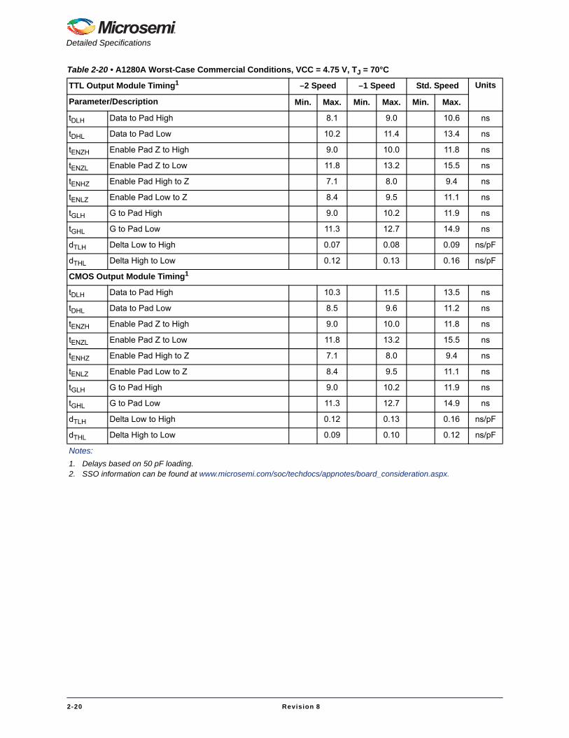
Table 2-20 • A1280A Worst-Case Commercial Conditions, VCC = 4.75 V, TJ = 70°C
TTL Output Module Timing1 –2 Speed –1 Speed Std. Speed Units
Parameter/Description Min. Max. Min. Max. Min. Max.
tDLH Data to Pad High 8.1 9.0 10.6 ns
tDHL Data to Pad Low 10.2 11.4 13.4 ns
tENZH Enable Pad Z to High 9.0 10.0 11.8 ns
tENZL Enable Pad Z to Low 11.8 13.2 15.5 ns
tENHZ Enable Pad High to Z 7.1 8.0 9.4 ns
tENLZ Enable Pad Low to Z 8.4 9.5 11.1 ns
tGLH G to Pad High 9.0 10.2 11.9 ns
tGHL G to Pad Low 11.3 12.7 14.9 ns
dTLH Delta Low to High 0.07 0.08 0.09 ns/pF
dTHL Delta High to Low 0.12 0.13 0.16 ns/pF
CMOS Output Module Timing1
tDLH Data to Pad High 10.3 11.5 13.5 ns
tDHL Data to Pad Low 8.5 9.6 11.2 ns
tENZH Enable Pad Z to High 9.0 10.0 11.8 ns
tENZL Enable Pad Z to Low 11.8 13.2 15.5 ns
tENHZ Enable Pad High to Z 7.1 8.0 9.4 ns
tENLZ Enable Pad Low to Z 8.4 9.5 11.1 ns
tGLH G to Pad High 9.0 10.2 11.9 ns
tGHL G to Pad Low 11.3 12.7 14.9 ns
dTLH Delta Low to High 0.12 0.13 0.16 ns/pF
dTHL Delta High to Low 0.09 0.10 0.12 ns/pF
Notes:1. Delays based on 50 pF loading.2. SSO information can be found at www.microsemi.com/soc/techdocs/appnotes/board_consideration.aspx.
2-20 Revision 8

ACT 2 Family FPGAs
Pin DescriptionsCLKA Clock A (Input)TTL Clock input for clock distribution networks. The Clock input is buffered prior to clocking the logicmodules. This pin can also be used as an I/O.
CLKB Clock B (Input)TTL Clock input for clock distribution networks. The Clock input is buffered prior to clocking the logicmodules. This pin can also be used as an I/O.
DCLK Diagnostic Clock (Input)TTL Clock input for diagnostic probe and device programming. DCLK is active when the MODE pin isHigh. This pin functions as an I/O when the MODE pin is Low.
GND GroundLow supply voltage.
I/O Input/Output (Input, Output)The I/O pin functions as an input, output, three-state, or bidirectional buffer. Input and output levels arecompatible with standard TTL and CMOS specifications. Unused I/O pins are automatically driven Lowby the ALS software.
MODE Mode (Input)The MODE pin controls the use of multifunction pins (DCLK, PRA, PRB, SDI). When the MODE pin isHigh, the special functions are active. When the MODE pin is Low, the pins function as I/Os. To provideActionprobe capability, the MODE pin should be terminated to GND through a 10K resistor so that theMODE pin can be pulled High when required.
NC No ConnectionThis pin is not connected to circuitry within the device.
PRA Probe A (Output) The Probe A pin is used to output data from any user-defined design node within the device. Thisindependent diagnostic pin can be used in conjunction with the Probe B pin to allow real-time diagnosticoutput of any signal path within the device. The Probe A pin can be used as a user-defined I/O whendebugging has been completed. The pin’s probe capabilities can be permanently disabled to protectprogrammed design confidentiality. PRA is active when the MODE pin is High. This pin functions as anI/O when the MODE pin is Low.
PRB Probe B (Output)The Probe B pin is used to output data from any user-defined design node within the device. Thisindependent diagnostic pin can be used in conjunction with the Probe A pin to allow real-time diagnosticoutput of any signal path within the device. The Probe B pin can be used as a user-defined I/O whendebugging has been completed. The pin’s probe capabilities can be permanently disabled to protectprogrammed design confidentiality. PRB is active when the MODE pin is High. This pin functions as anI/O when the MODE pin is Low.
SDI Serial Data Input (Input)Serial data input for diagnostic probe and device programming. SDI is active when the MODE pin is High.This pin functions as an I/O when the MODE pin is Low.
SDO Serial Data Output (Output)Serial data output for diagnostic probe. SDO is active when the MODE pin is High. This pin functions asan I/O when the MODE pin is Low.
VCC 5.0 V Supply VoltageHigh supply voltage.
Revision 8 2-21


3 – Package Pin Assignments
PL84
NoteFor Package Manufacturing and Environmental information, visit the Resource Center athttp://www.microsemi.com/soc/products/solutions/package/docs.aspx.
12
13
14
15
16
18
17
19
20
21
22
23
24
25
26
27
28
29
30
31
32
74
73
72
71
70
68
69
67
66
65
64
63
62
61
60
59
58
57
56
55
54
33 34 35 36 37 38 39 40 41 42 43 44 45 46 47 48 49 50 51 52 53
11 10 9 8 7 6 5 4 3 2 1 84 83 82 81 80 79 78 77 76 75
84-PinPLCC
Revision 8 3-1

Package Pin Assignments
Notes:1. All unlisted pin numbers are user I/Os.2. MODE pin should be terminated to GND through a 10K resistor to enable Actionprobe usage; otherwise it can
be terminated directly to GND.
PL84
Pin Number A1225A Function A1240A Function A1280A Function
2 CLKB, I/O CLKB, I/O CLKB, I/O
4 PRB, I/O PRB, I/O PRB, I/O
6 GND GND GND
10 DCLK, I/O DCLK, I/O DCLK, I/O
12 MODE MODE MODE
22 VCC VCC VCC
23 VCC VCC VCC
28 GND GND GND
43 VCC VCC VCC
49 GND GND GND
52 SDO SDO SDO
63 GND GND GND
64 VCC VCC VCC
65 VCC VCC VCC
70 GND GND GND
76 SDI, I/O SDI, I/O SDI, I/O
81 PRA, I/O PRA, I/O PRA, I/O
83 CLKA, I/O CLKA, I/O CLKA, I/O
84 VCC VCC VCC
3-2 Revision 8

ACT 2 Family FPGAs
PQ100
NoteFor Package Manufacturing and Environmental information, visit the Resource Center athttp://www.microsemi.com/soc/products/solutions/package/docs.aspx
100-PinPQFP
81828384858687888990919293949596979899100
5049484746454443424140393837363534333231
80 79 78 77 76 75 74 73 72 71 70 69 68 67 66 65 64 63 62 61 60 59 58 57 56 55 54 53 52 51
1 2 3 4 5 6 7 8 9 10 11 12 13 14 15 16 17 18 19 20 21 22 23 24 25 26 27 28 29 30
Revision 8 3-3

Package Pin Assignments
Notes:1. All unlisted pin numbers are user I/Os.2. MODE pin should be terminated to GND through a 10K resistor to enable Actionprobe usage; otherwise it can
be terminated directly to GND.
PQ100
Pin Number A1225A Function
2 DCLK, I/O
4 MODE
9 GND
16 VCC
17 VCC
22 GND
34 GND
40 VCC
46 GND
52 SDO
57 GND
64 GND
65 VCC
66 VCC
67 VCC
72 GND
79 SDI, I/O
84 GND
87 PRA, I/O
89 CLKA, I/O
90 VCC
92 CLKB, I/O
94 PRB, I/O
96 GND
PQ100
Pin Number A1225A Function
3-4 Revision 8

ACT 2 Family FPGAs
PQ144
NoteFor Package Manufacturing and Environmental information, visit the Resource Center athttp://www.microsemi.com/soc/products/solutions/package/docs.aspx
144
1
144-PinPQFP
Revision 8 3-5

Package Pin Assignments
Notes:1. All unlisted pin numbers are user I/Os.2. MODE pin should be terminated to GND through a 10K resistor to enable Actionprobe usage; otherwise it can
be terminated directly to GND.
PQ144
Pin Number A1240A Function
2 MODE
9 GND
10 GND
11 GND
18 VCC
19 VCC
20 VCC
21 VCC
28 GND
29 GND
30 GND
44 GND
45 GND
46 GND
54 VCC
55 VCC
56 VCC
64 GND
65 GND
71 SDO
79 GND
80 GND
81 GND
88 GND
89 VCC
90 VCC
91 VCC
92 VCC
93 VCC
100 GND
101 GND
102 GND
110 SDI, I/O
116 GND
117 GND
118 GND
123 PRA, I/O
125 CLKA, I/O
126 VCC
127 VCC
128 VCC
130 CLKB, I/O
132 PRB, I/O
136 GND
137 GND
138 GND
144 DCLK, I/O
PQ144
Pin Number A1240A Function
3-6 Revision 8

ACT 2 Family FPGAs
PQ160
NoteFor Package Manufacturing and Environmental information, visit the Resource Center athttp://www.microsemi.com/soc/products/solutions/package/docs.aspx
Note: This is the top view of the package
12011911811711611511411311211111010910810710610510410310210110099989796959493929190898887868584838281
160
159
158
157
156
155
154
153
152
151
150
149
148
147
146
145
144
143
142
141
140
139
138
137
136
135
134
133
132
131
130
129
128
127
126
125
124
123
122
121
41 42 43 44 45 46 47 48 49 50 51 52 53 54 55 56 57 58 59 60 61 62 63 64 65 66 67 68 69 70 71 72 73 74 75 76 77 78 79 80
123456789
10111213141516171819202122232425262728293031323334353637383940
160-PinPQFP
Revision 8 3-7

Package Pin Assignments
Notes:1. All unlisted pin numbers are user I/Os.2. MODE pin should be terminated to GND through a 10K resistor to enable Actionprobe usage; otherwise it can
be terminated directly to GND.
PQ160
Pin Number A1280A Function
2 DCLK, I/O
6 VCC
11 GND
16 PRB, I/O
18 CLKB, I/O
20 VCC
21 CLKA, I/O
23 PRA, I/O
30 GND
35 VCC
38 SDI, I/O
40 GND
44 GND
49 GND
54 VCC
57 VCC
58 VCC
59 GND
60 VCC
61 GND
64 GND
69 GND
80 GND
82 SDO
86 VCC
89 GN
98 GND
99 GND
109 GND
114 VCC
120 GND
125 GND
130 GND
135 VCC
138 VCC
139 VCC
140 GND
145 GND
150 VCC
155 GND
159 MODE
160 GND
PQ160
Pin Number A1280A Function
3-8 Revision 8
ACT 2 Family FPGAs
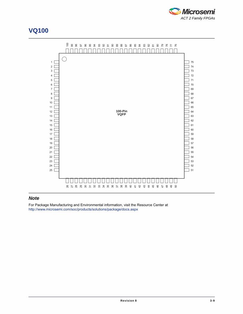
VQ100
NoteFor Package Manufacturing and Environmental information, visit the Resource Center athttp://www.microsemi.com/soc/products/solutions/package/docs.aspx
1
23
4
5
7
6
8
9
10
11
12
13
14
15
16
17
18
19
20
21
22
23
24
25
100-PinVQFP
75
7473
72
71
69
70
68
67
66
65
64
63
62
61
60
59
58
57
56
55
54
53
52
51
26 27 28 29 30 3231 33 34 35 36 37 38 39 40 41 42 43 44 45 46 47 48 49 50
100
99 98 97 96 9495 93 92 91 90 89 88 87 86 85 84 83 82 81 80 79 78 77 76
Revision 8 3-9

Package Pin Assignments
Notes:1. All unlisted pin numbers are user I/Os.2. MODE pin should be terminated to GND through a 10K resistor to enable Actionprobe usage; otherwise it can
be terminated directly to GND.
VQ100
Pin Number A1225A Function
2 MODE
7 GND
14 VCC
15 VCC
20 GND
32 GND
38 VCC
44 GND
50 SDO
55 GND
62 GND
63 VCC
64 VCC
65 VCC
70 GND
77 SDI, I/O
82 GND
85 PRA, I/O
87 CLKA, I/O
88 VCC
90 CLKB, I/O
92 PRB, I/O
94 GND
100 DCLK, I/O
VQ100
Pin Number A1225A Function
3-10 Revision 8
ACT 2 Family FPGAs
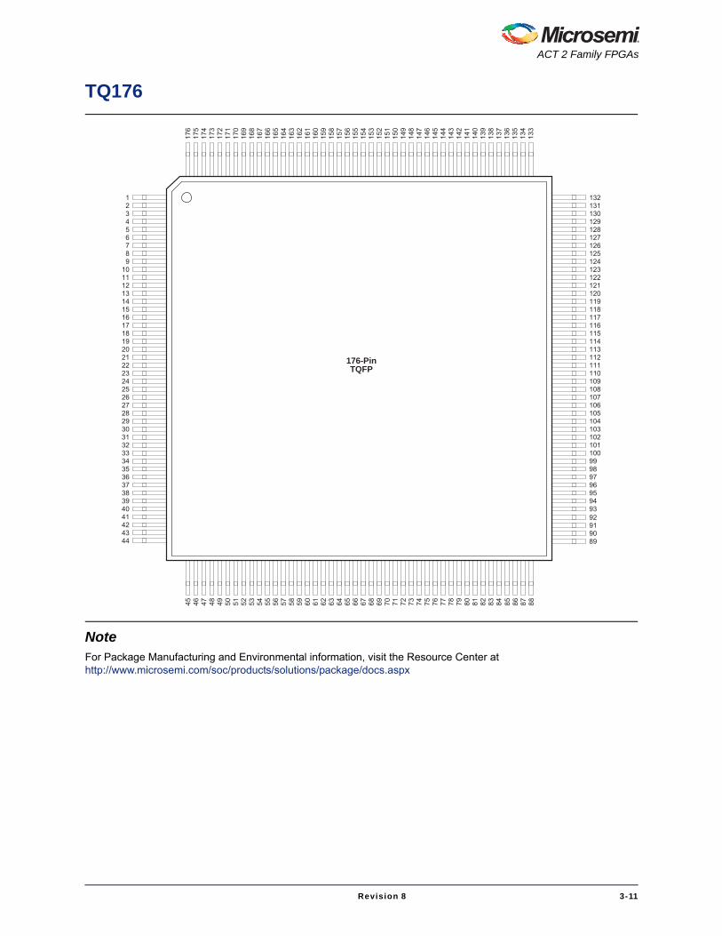
TQ176
NoteFor Package Manufacturing and Environmental information, visit the Resource Center athttp://www.microsemi.com/soc/products/solutions/package/docs.aspx
45 46 47 48 49 50 51 52 53 54 55 56 57 58 59 60 61 62 63 64 65 66 67 68 69 70 71 72 73 74 75 76 77 78 79 80 81 82 83 84 85 86 87 88
41424344
176
175
174
173
172
171
170
169
168
167
166
165
164
163
162
161
160
159
158
157
156
155
154
153
152
151
150
149
148
147
146
145
144
143
142
141
123456789
10111213141516171819202122232425262728293031323334353637383940
140
139
138
137
176-PinTQFP
1321311301291281271261251241231221211201191181171161151141131121111101091081071061051041031021011009998979695949392919089
136
135
134
133
Revision 8 3-11

Package Pin Assignments
TQ176
Pin Number A1240A Function A1280A Function
1 GND GND
2 MODE MODE
8 NC NC
10 NC I/O
11 NC I/O
13 NC VCC
18 GND GND
19 NC I/O
20 NC I/O
22 NC I/O
23 GND GND
24 NC VCC
25 VCC VCC
26 NC I/O
27 NC I/O
28 VCC VCC
29 NC I/O
33 NC NC
37 NC I/O
38 NC NC
45 GND GND
52 NC VCC
54 NC I/O
55 NC I/O
57 NC NC
61 NC I/O
64 NC I/O
66 NC I/O
67 GND GND
68 VCC VCC
74 NC I/O
77 NC NC
78 NC I/O
80 NC I/O
82 NC VCC
86 NC I/O
87 SDO SDO
89 GND GND
96 NC I/O
97 NC I/O
101 NC NC
103 NC I/O
106 GND GND
107 NC I/O
108 NC I/O
109 GND GND
110 VCC VCC
111 GND GND
112 VCC VCC
113 VCC VCC
114 NC I/O
115 NC I/O
116 NC VCC
121 NC NC
124 NC I/O
125 NC I/O
126 NC NC
133 GND GND
135 SDI, I/O SDI, I/O
136 NC I/O
140 NC VCC
143 NC I/O
144 NC I/O
145 NC NC
147 NC I/O
151 NC I/O
152 PRA, I/O PRA, I/O
154 CLKA, I/O CLKA, I/O
TQ176
Pin Number A1240A Function A1280A Function
3-12 Revision 8

ACT 2 Family FPGAs
Notes:1. NC denotes no connection.2. All unlisted pin numbers are user I/Os.3. MODE pin should be terminated to GND through a 10K resistor to enable Actionprobe usage; otherwise it can
be terminated directly to GND.
155 VCC VCC
156 GND GND
158 CLKB, I/O CLKB, I/O
160 PRB, I/O PRB, I/O
161 NC I/O
165 NC NC
166 NC I/O
168 NC I/O
170 NC VCC
173 NC I/O
175 DCLK, I/O DCLK, I/O
TQ176
Pin Number A1240A Function A1280A Function
Revision 8 3-13

Package Pin Assignments
CQ172
NoteFor Package Manufacturing and Environmental information, visit the Resource Center athttp://www.microsemi.com/soc/products/solutions/package/docs.aspx
172-PinCQFP
Pin #1Index
172
1
3-14 Revision 8

ACT 2 Family FPGAs
Notes:1. All unlisted pin numbers are user I/Os.2. MODE pin should be terminated to GND through a 10K resistor to enable Actionprobe usage; otherwise it can
be terminated directly to GND.
CQ172
Pin Number A1280A Function
1 MODE
7 GND
12 VCC
17 GND
22 GND
23 VCC
24 VCC
27 VCC
32 GND
37 GND
50 VCC
55 GND
65 GND
66 VCC
75 GND
80 VCC
85 SDO
98 GND
103 GND
106 GND
107 VCC
108 GND
109 VCC
110 VCC
113 VCC
118 GND
123 GND
131 SDI, I/O
136 VCC
141 GND
148 PRA, I/O
150 CLKA, I/O
151 VCC
152 GND
154 CLKB, I/O
156 PRB, I/O
161 GND
166 VCC
171 DCLK, I/O
CQ172
Pin Number A1280A Function
Revision 8 3-15

Package Pin Assignments
PG100
NoteFor Package Manufacturing and Environmental information, visit the Resource Center athttp://www.microsemi.com/soc/products/solutions/package/docs.aspx
1
A
2 3 4 5 6 7 8 9 10 11
B
C
D
E
F
G
H
J
K
L
A
B
C
D
E
F
G
H
J
K
L
100-PinCPGA
1 2 3 4 5 6 7 8 9 10 11
Orientation Pin
3-16 Revision 8

ACT 2 Family FPGAs
Notes:1. All unlisted pin numbers are user I/Os.2. MODE pin should be terminated to GND through a 10K resistor to enable Actionprobe usage; otherwise it can
be terminated directly to GND.
PG100
Pin Number A1225A Function
A4 PRB, I/O
A7 PRA, I/O
B6 VCC
C2 MODE
C3 DCLK, I/O
C5 GND
C6 CLKA, I/O
C7 GND
C8 SDI, I/O
D6 CLKB, I/O
D10 GND
E3 GND
E11 VCC
F3 VCC
F9 VCC
F10 VCC
F11 GND
G1 VCC
G3 GND
G9 GND
J5 GND
J7 GND
J9 SDO
K6 VCC
PG100
Pin Number A1225A Function
Revision 8 3-17
Package Pin Assignments
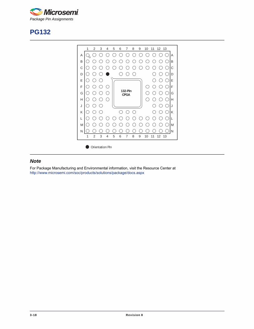
PG132
NoteFor Package Manufacturing and Environmental information, visit the Resource Center athttp://www.microsemi.com/soc/products/solutions/package/docs.aspx
132-PinCPGA
A
B
C
D
E
F
G
H
J
K
L
M
N
A
B
C
D
E
F
G
H
J
K
L
M
N
Orientation Pin
1 2 3 4 5 6 7 8 9 10 11 12 13
1 2 3 4 5 6 7 8 9 10 11 12 13
3-18 Revision 8

ACT 2 Family FPGAs
Notes:1. All unlisted pin numbers are user I/Os.2. MODE pin should be terminated to GND through a 10K resistor to enable Actionprobe usage; otherwise it can
be terminated directly to GND.
PG132
Pin Number A1240A Function
A1 MODE
B5 GND
B6 CLKB, I/O
B7 CLKA, I/O
B8 PRA, I/O
B9 GND
B12 SDI, I/O
C3 DCLK, I/O
C5 GND
C6 PRB, I/O
C7 VCC
C9 GND
D7 VCC
E3 GND
E11 GND
E12 GND
F4 GND
G2 VCC
G3 VCC
G4 VCC
G10 VCC
G11 VCC
G12 VCC
G13 VCC
H13 GND
J2 GND
J3 GND
J11 GND
K7 VCC
K12 GND
L5 GND
L7 VCC
L9 GND
M9 GND
N12 SDO
PG132
Pin Number A1240A Function
Revision 8 3-19
Package Pin Assignments
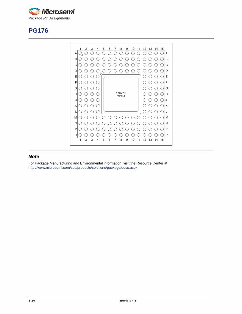
PG176
NoteFor Package Manufacturing and Environmental information, visit the Resource Center athttp://www.microsemi.com/soc/products/solutions/package/docs.aspx
1
A
2 3 4 5 6 7 8 9 10 11
B
C
D
E
F
G
H
J
K
L
176-PinCPGA
1 2 3 4 5 6 7 8 9 10 11
12
12
13
13
14
14
15
15
M
N
P
R
A
B
C
D
E
F
G
H
J
K
L
M
N
P
R
3-20 Revision 8

ACT 2 Family FPGAs
Notes:1. All unlisted pin numbers are user I/Os.2. MODE pin should be terminated to GND through a 10K resistor to enable Actionprobe usage; otherwise it can
be terminated directly to GND.
PG176
Pin Number A1280A Function
A9 CLKA, I/O
B3 DCLK, I/O
B8 CLKB, I/O
B14 SDI, I/O
C3 MODE
C8 GND
C9 PRA, I/O
D4 GND
D5 VCC
D6 GND
D7 PRB, I/O
D8 VCC
D10 GND
D11 VCC
D12 GND
E4 GND
E12 GND
F4 VCC
F12 GND
G4 GND
G12 VCC
H2 VCC
H3 VCC
H4 GND
H12 GND
H13 VCC
H14 VCC
J4 VCC
J12 GND
J13 GND
J14 VCC
K4 GND
K12 GND
L4 GND
M4 GND
M5 VCC
M6 GND
M8 GND
M10 GND
M11 VCC
M12 GND
N8 VCC
P13 SDO
PG176
Pin Number A1280A Function
Revision 8 3-21


4 – Datasheet Information
List of ChangesThe following table lists critical changes that were made in each version of the datasheet.
Revision Changes Page
Revision 8(January 2012)
The ACT 2 datasheet was formatted newly in the style used for current datasheets.The same information is present (other than noted in the list of changes for thisrevision) but divided into chapters.
N/A
Package names used in Table 1 • ACT 2 Product Family Profile and throughout thedocument were revised to match standards given in Package Mechanical Drawings(SAR 27395).
I
The description for SDO pins had earlier been removed from the datasheet and hasnow been included again, in the "Pin Descriptions" section (SAR 35819).
2-21
SDO pin numbers had earlier been removed from package pin assignment tables inthe datasheet, and have now been restored to the pin tables (SAR 35819).
3-2
Revision 7(June 2006)
The "Ordering Information" section was revised to include RoHS information. II
Revision 6(December 2000)
In the "PG176" package, pin A3 was incorrectly assigned as CLKA, I/O. A3 is a userI/O. Pin A9 is CLKA, I/O.
3-21
Revision 8 4-1
Datasheet Information
Datasheet CategoriesCategoriesIn order to provide the latest information to designers, some datasheet parameters are published beforedata has been fully characterized from silicon devices. The data provided for a given device isdesignated as either "Product Brief," "Advance," "Preliminary," or "Production." The definitions of thesecategories are as follows:
Product BriefThe product brief is a summarized version of a datasheet (advance or production) and contains generalproduct information. This document gives an overview of specific device and family information.
AdvanceThis version contains initial estimated information based on simulation, other products, devices, or speedgrades. This information can be used as estimates, but not for production. This label only applies to theDC and Switching Characteristics chapter of the datasheet and will only be used when the data has notbeen fully characterized.
PreliminaryThe datasheet contains information based on simulation and/or initial characterization. The information isbelieved to be correct, but changes are possible.
ProductionThis version contains information that is considered to be final.
Export Administration Regulations (EAR) The products described in this document are subject to the Export Administration Regulations (EAR).They could require an approved export license prior to export from the United States. An export includesrelease of product or disclosure of technology to a foreign national inside or outside the United States.
Safety Critical, Life Support, and High-Reliability Applications Policy
The products described in this advance status document may not have completed the Microsemiqualification process. Products may be amended or enhanced during the product introduction andqualification process, resulting in changes in device functionality or performance. It is the responsibility ofeach customer to ensure the fitness of any product (but especially a new product) for a particularpurpose, including appropriateness for safety-critical, life-support, and other high-reliability applications.Consult the Microsemi SoC Products Group Terms and Conditions for specific liability exclusions relatingto life-support applications. A reliability report covering all of the SoC Products Group’s products isavailable at http://www.microsemi.com/soc/documents/ORT_Report.pdf. Microsemi also offers a varietyof enhanced qualification and lot acceptance screening procedures. Contact your local sales office foradditional reliability information.
4-2 Revision 8


5172104-8/1.12
© 2012 Microsemi Corporation. All rights reserved. Microsemi and the Microsemi logo are trademarks ofMicrosemi Corporation. All other trademarks and service marks are the property of their respective owners.
Microsemi Corporation (NASDAQ: MSCC) offers a comprehensive portfolio of semiconductorsolutions for: aerospace, defense and security; enterprise and communications; and industrialand alternative energy markets. Products include high-performance, high-reliability analog andRF devices, mixed signal and RF integrated circuits, customizable SoCs, FPGAs, andcomplete subsystems. Microsemi is headquartered in Aliso Viejo, Calif. Learn more atwww.microsemi.com.
Microsemi Corporate HeadquartersOne Enterprise, Aliso Viejo CA 92656 USAWithin the USA: +1 (949) 380-6100Sales: +1 (949) 380-6136Fax: +1 (949) 215-4996