A Study on Full Digital Clock Data Recovery (CDR) CDR Fundamentals Preamble bits Timing get sample...
30
1 Philipus Oh, Win Chaivipas, Akira Matsuzawa Tokyo Institute of Technology Graduate School of Science and Engineering Department of Physical Electronics Matsuzawa Laboratory A Study on Full Digital Clock Data Recovery (CDR) Matsuzawa Lab. Tokyo Institute of Technology
-
Upload
truongdung -
Category
Documents
-
view
219 -
download
0
Transcript of A Study on Full Digital Clock Data Recovery (CDR) CDR Fundamentals Preamble bits Timing get sample...

1
Philipus Oh, Win Chaivipas, Akira Matsuzawa
Tokyo Institute of TechnologyGraduate School of Science and Engineering
Department of Physical ElectronicsMatsuzawa Laboratory
A Study on Full Digital Clock Data Recovery (CDR)
Matsuzawa Lab.Tokyo Institute of Technology
2
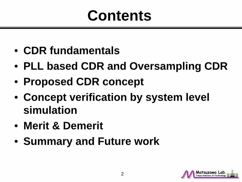
Contents
• CDR fundamentals • PLL based CDR and Oversampling CDR • Proposed CDR concept • Concept verification by system level
simulation• Merit & Demerit• Summary and Future work
Matsuzawa Lab.Tokyo Institute of Technology

3
CDR Fundamentals
Preamblebits Timing
get sample Incoming Data
A part of receiver that:
QD
pre-amplifier
Clock DataRecovery
Data out
VTT
Datain
Receiver
QD
-VTT
QD QD
V
Preamble bits (to make sure CLK information is obtained before sampling the data)
Data
Matsuzawa Lab.Tokyo Institute of Technology
4
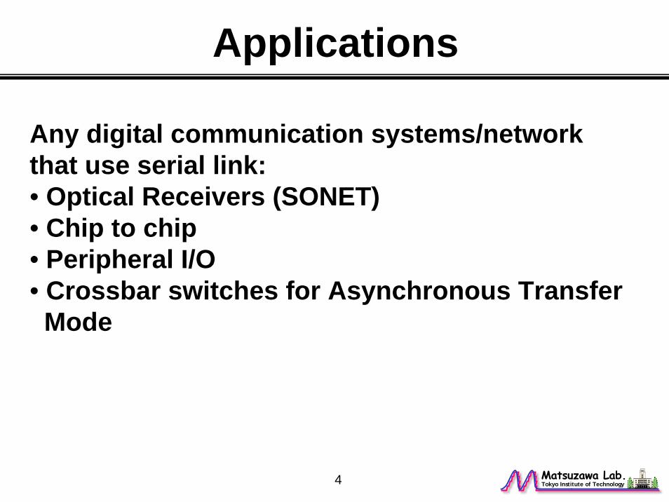
Applications
Any digital communication systems/network that use serial link:• Optical Receivers (SONET)• Chip to chip• Peripheral I/O• Crossbar switches for Asynchronous Transfer Mode
Matsuzawa Lab.Tokyo Institute of Technology
5
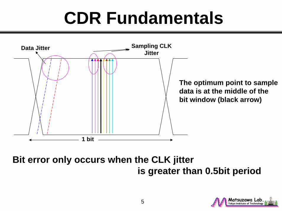
CDR FundamentalsData Jitter Sampling CLK
Jitter
1 bit
The optimum point to sample data is at the middle of the bit window (black arrow)
Bit error only occurs when the CLK jitter is greater than 0.5bit period
Matsuzawa Lab.Tokyo Institute of Technology
6
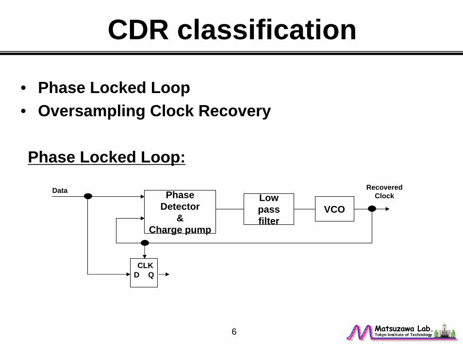
CDR classification
• Phase Locked Loop• Oversampling Clock Recovery
Phase Locked Loop:
Low passfilter
Phase Detector
&Charge pump
VCO
DCLK
Q
Data RecoveredClock
Matsuzawa Lab.Tokyo Institute of Technology

7
PLL based CDR
Data
CLK
Y
B
A
X
Data
CLK
Y
B
A
X
Phase detector in PLL for CDR must be able to detect edges and phase difference in random data.
Classified into:• Hogge’s Analog Phase Detector• Alexander Binary Phase Detector
Hogge’s Phase detector Timing Waveform Transfer Function
The difference between X & Y will show the phase difference amount and polarity Matsuzawa Lab.Tokyo Institute of Technology

8
PLL based CDR
Y
XD Q D QData
CLK
D Q D Q
Q1
Q2
Q3
Q4
X
Y
Alexander Binary PD Timing Waveform Transfer Function
When data edge leads
When CLK edge leads
The result of phase detection only tells the polarity,whether leading or lagging.
Thus, jitter is constantly produced at every phase detectionThe amount of phase difference is not detected
Matsuzawa Lab.Tokyo Institute of Technology

9
PLL Issue
• Low frequency acquisition, within 25% of VCO center frequency
• Long lock time, about 100 preamble data(depends on bandwidth, which also affect jitter performance, there’s a trade off)
• Possibility of harmonic lock
Matsuzawa Lab.Tokyo Institute of Technology
10
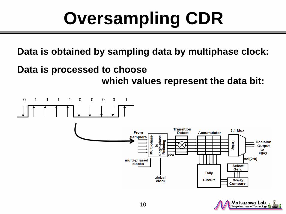
Oversampling CDR
Data is obtained by sampling data by multiphase clock:
Data is processed to choose which values represent the data bit:
Matsuzawa Lab.Tokyo Institute of Technology
0 11 011 00 0 1
11
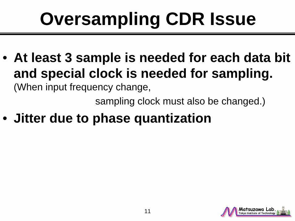
Oversampling CDR Issue
• At least 3 sample is needed for each data bit and special clock is needed for sampling.(When input frequency change,
sampling clock must also be changed.)
• Jitter due to phase quantization
Matsuzawa Lab.Tokyo Institute of Technology

12
Proposed CDR Intro
The proposed CDR is maintained to sample around the middle of the bit window (colourful arrows)
But NEVER at the middle of bit window!!
Data Jitter Sampling CLKJitter
1 bit
Matsuzawa Lab.Tokyo Institute of Technology

13
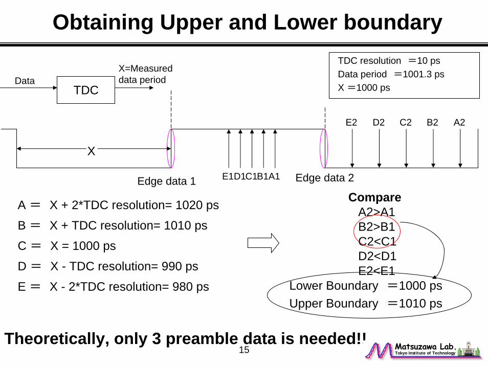
X
TDCData
X=Measured data period
Data period =1001.3 psTDC resolution =10 psExample:
Proposed CDR
Due to the fact that △Ф=△ω.T, if we use X directly,large BER will occur:
= sampling using X as sampling period
=sampling using ideal data period
=sampling error
X=1000 ps or 1010 ps
Matsuzawa Lab.Tokyo Institute of Technology

14
Alternate Sampling
= 1010 ps (Upper boundary)
= 1000 ps (Lower boundary)
If we use this sampling period alternately :
Data period = 1001.3 psTDC resolution = 10 ps
Error will not occur !
Data period lies within 1000 ps and 1010 ps(TDC step interval)
= ideal sampling point= sampling point using result from TDC directly
Matsuzawa Lab.Tokyo Institute of Technology
15
Data period =1001.3 psTDC resolution =10 ps
X =1000 ps
A = X + 2*TDC resolution= 1020 ps
B = X + TDC resolution= 1010 ps
C = X = 1000 ps
D = X - TDC resolution= 990 ps
E = X - 2*TDC resolution= 980 ps Lower Boundary =1000 psUpper Boundary =1010 ps
A2>A1B2>B1C2<C1D2<D1E2<E1
Compare
Obtaining Upper and Lower boundary
Theoretically, only 3 preamble data is needed!! Matsuzawa Lab.Tokyo Institute of Technology
X
TDCData
X=Measured data period
Edge data 1 A1B1C1D1E1 Edge data 2
A2B2C2D2E2
16
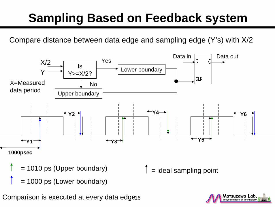
Sampling Based on Feedback systemCompare distance between data edge and sampling edge (Y’s) with X/2
Comparison is executed at every data edge
Y1
Y2
1000psec
Y3
Y4
Y5
Y6
Data in Data out
Is Y>=X/2?
Upper boundary
Lower boundaryYes
No
X/2Y
= 1010 ps (Upper boundary)
= 1000 ps (Lower boundary)= ideal sampling point
X=Measured data period
Matsuzawa Lab.Tokyo Institute of Technology
17
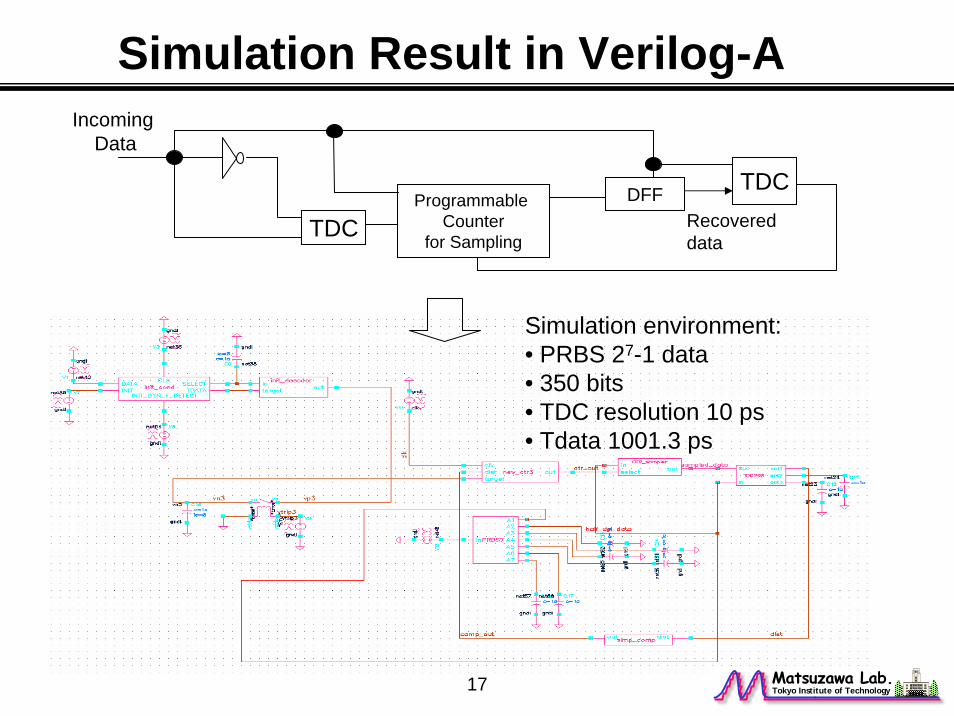
TDCDFF
TDCProgrammable
Counterfor Sampling
Incoming Data
Recovered data
Simulation Result in Verilog-A
Simulation environment:• PRBS 27-1 data• 350 bits• TDC resolution 10 ps• Tdata 1001.3 ps
Matsuzawa Lab.Tokyo Institute of Technology

18
Y1
Y2
1000psec
Y3
Y4
Y5
Y6
Simulation Result in Verilog-AY(psec)
Time (nsec)
Y value is maintained around halfbit period (500.65 ps)
ideal500.65ps
Matsuzawa Lab.Tokyo Institute of Technology
19
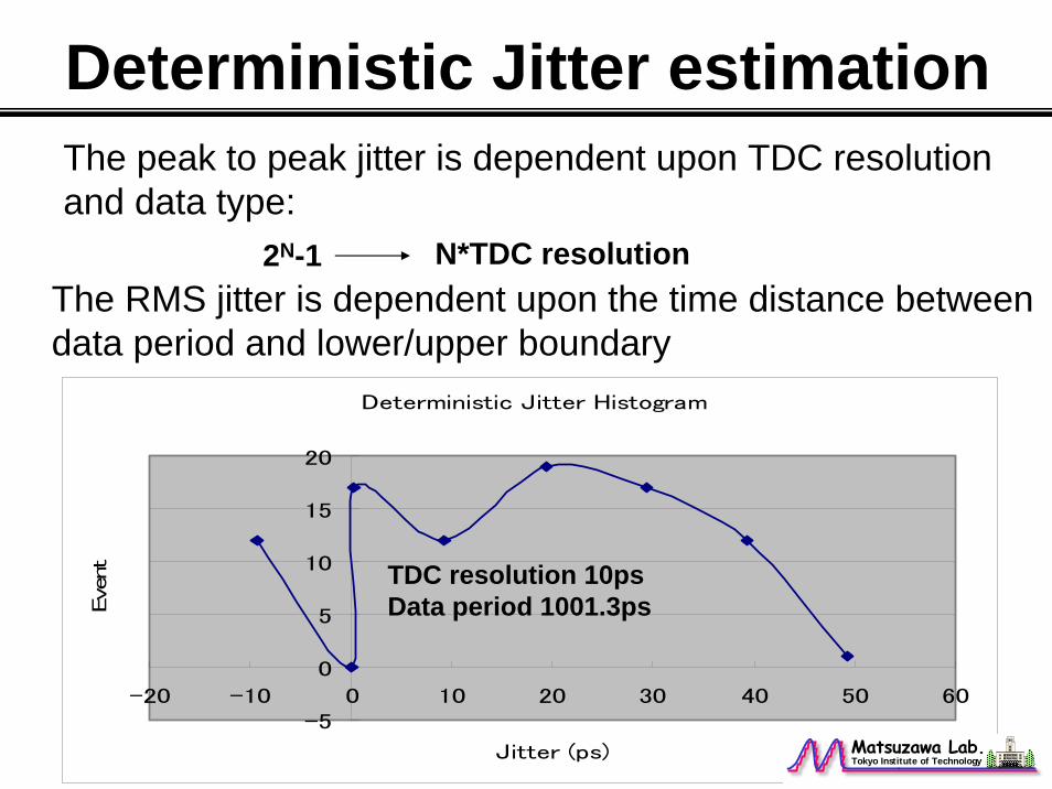
Deterministic Jitter estimationThe peak to peak jitter is dependent upon TDC resolution and data type:
2N-1 N*TDC resolution The RMS jitter is dependent upon the time distance between data period and lower/upper boundary
Deterministic Jitter Histogram
-5
0
5
10
15
20
-20 -10 0 10 20 30 40 50 60
Jitter (ps)
Event TDC resolution 10ps
Data period 1001.3ps
Matsuzawa Lab.Tokyo Institute of Technology
20
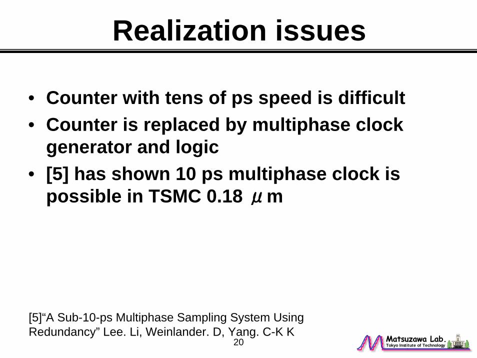
Realization issues
• Counter with tens of ps speed is difficult• Counter is replaced by multiphase clock
generator and logic• [5] has shown 10 ps multiphase clock is
possible in TSMC 0.18 μm
[5]“A Sub-10-ps Multiphase Sampling System Using Redundancy” Lee. Li, Weinlander. D, Yang. C-K K
Matsuzawa Lab.Tokyo Institute of Technology

21
Clock Recovery Stage
Matsuzawa Lab.Tokyo Institute of Technology
22
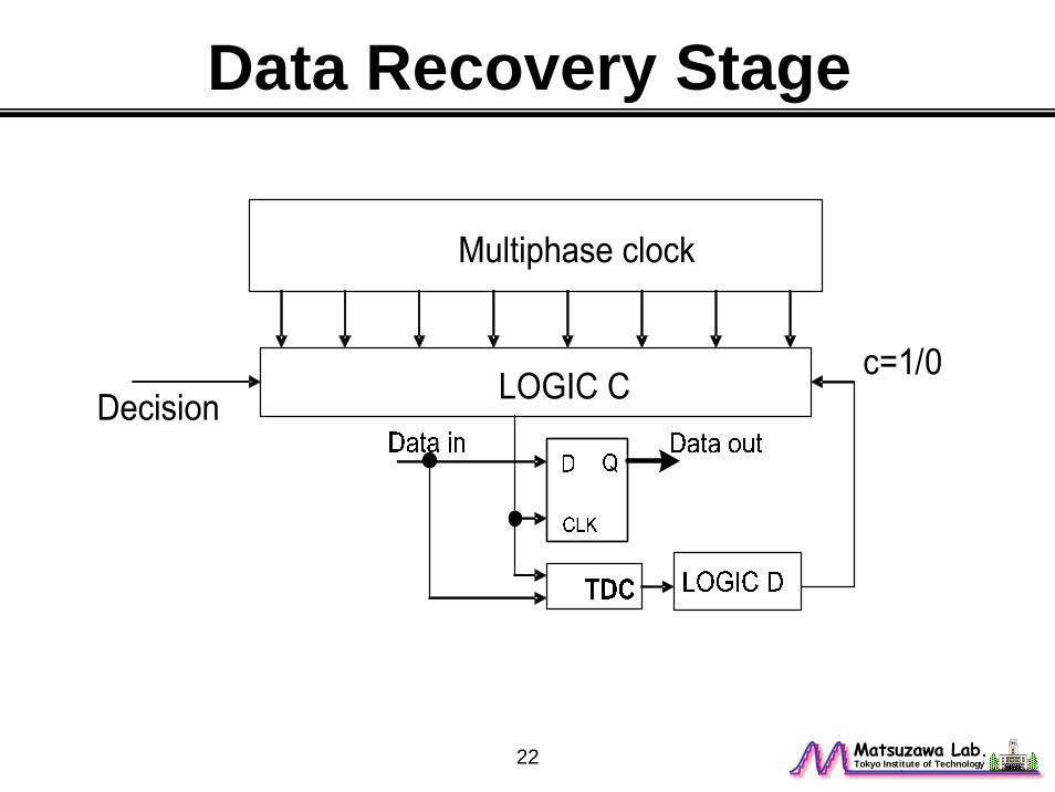
Data Recovery Stage
Matsuzawa Lab.Tokyo Institute of Technology

23
With logic and ideal Multiphase clockY value
Less than 5 preamble data was used
Matsuzawa Lab.Tokyo Institute of Technology
24
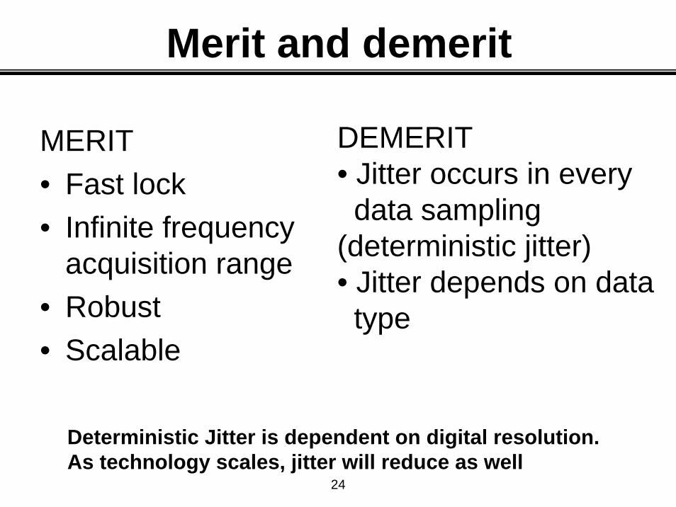
Merit and demerit
MERIT• Fast lock• Infinite frequency
acquisition range• Robust• Scalable
DEMERIT• Jitter occurs in every data sampling
(deterministic jitter)• Jitter depends on data type
Deterministic Jitter is dependent on digital resolution. As technology scales, jitter will reduce as well
25
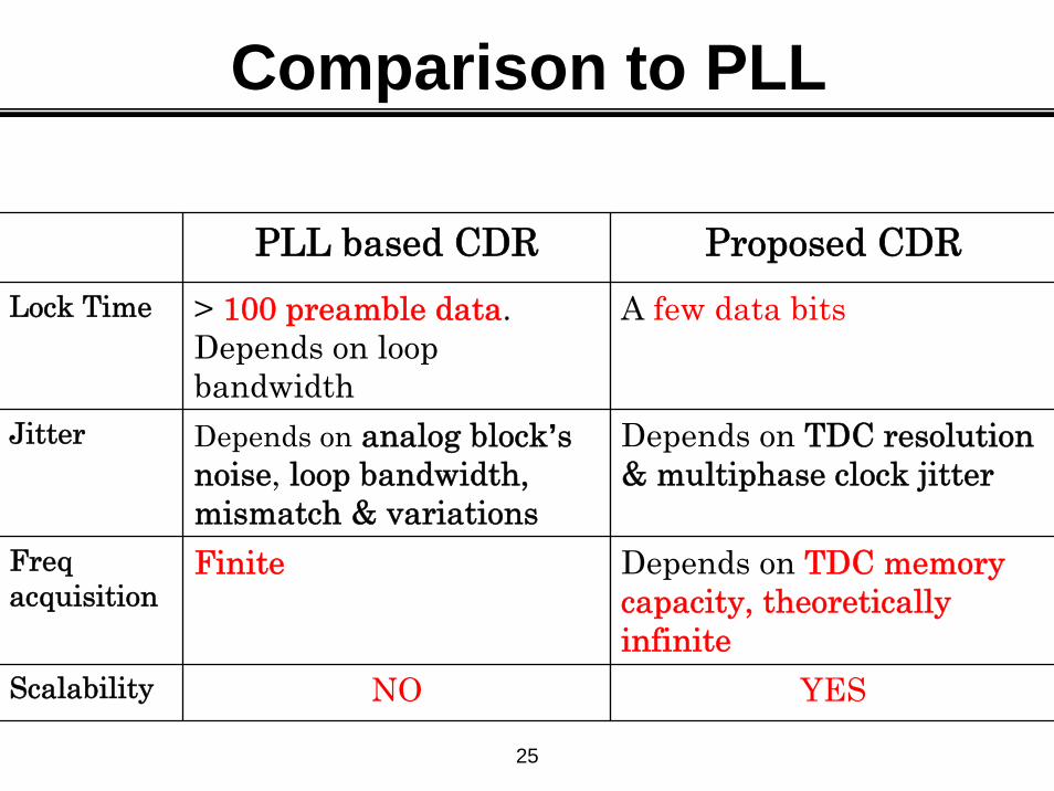
Comparison to PLL
PLL based CDR Proposed CDRLock Time > 100 preamble data.
Depends on loopbandwidth
A few data bits
Jitter Depends on analog block’s noise, loop bandwidth, mismatch & variations
Depends on TDC resolution & multiphase clock jitter
Freq acquisition
Finite Depends on TDC memory capacity, theoretically infinite
Scalability NO YES

26
Comparison to OversamplingOversampling CDR Proposed CDR
Lock Time Within a few data bits Within a few data bits
Jitter Depends on multiphase clock jitter
Depends on TDC resolution & multiphase clock jitter
Response to Change ofInput freq
Take time for the multiphase clock to relock
Fast, only a few data bits
Scalability YES YES

27
Comparison
PRBS 28-1 P-P Jitter 280 ps
[1] “An Auto-Ranging 50-210Mb/s Clock Recovery Circuit with Time-to-Digital Converter”. ISSCC’99, Seoul National University
Use 3 analog loop, lock time takes several μsec
Matsuzawa Lab.Tokyo Institute of Technology
28
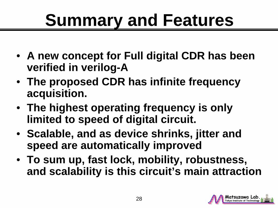
Summary and Features
• A new concept for Full digital CDR has been verified in verilog-A
• The proposed CDR has infinite frequency acquisition.
• The highest operating frequency is only limited to speed of digital circuit.
• Scalable, and as device shrinks, jitter and speed are automatically improved
• To sum up, fast lock, mobility, robustness, and scalability is this circuit’s main attraction
Matsuzawa Lab.Tokyo Institute of Technology

29
Future Works
• Phase detection and Phase compensation circuit
• Improvements against data jitter (Jitter tolerance)
Matsuzawa Lab.Tokyo Institute of Technology
30
Reference
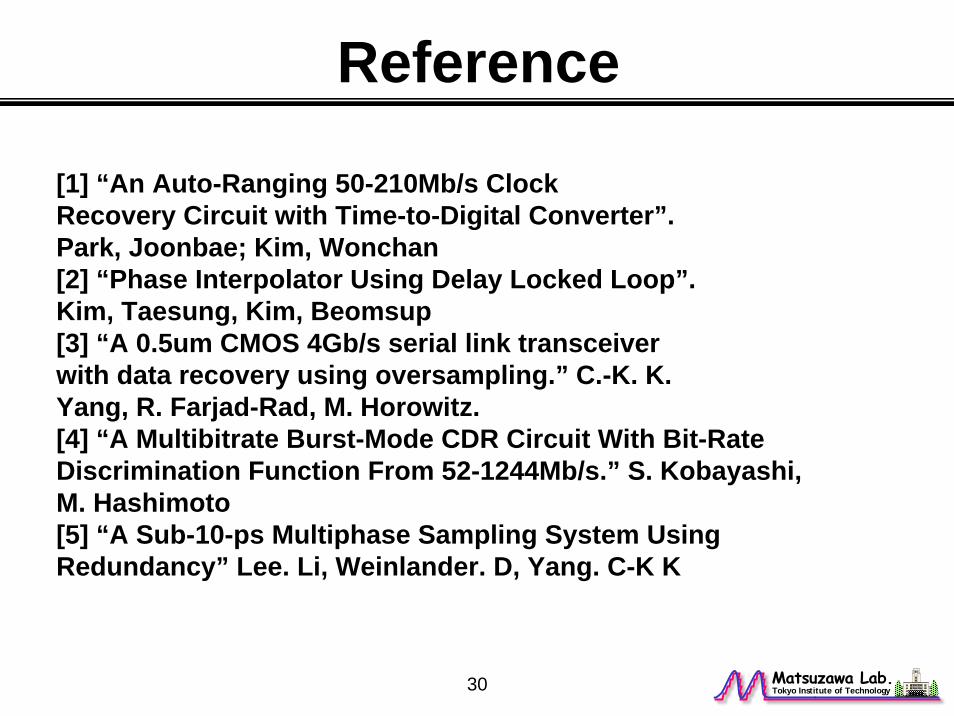
[1] “An Auto-Ranging 50-210Mb/s Clock Recovery Circuit with Time-to-Digital Converter”. Park, Joonbae; Kim, Wonchan[2] “Phase Interpolator Using Delay Locked Loop”. Kim, Taesung, Kim, Beomsup[3] “A 0.5um CMOS 4Gb/s serial link transceiver with data recovery using oversampling.” C.-K. K. Yang, R. Farjad-Rad, M. Horowitz.[4] “A Multibitrate Burst-Mode CDR Circuit With Bit-Rate Discrimination Function From 52-1244Mb/s.” S. Kobayashi, M. Hashimoto[5] “A Sub-10-ps Multiphase Sampling System Using Redundancy” Lee. Li, Weinlander. D, Yang. C-K K
Matsuzawa Lab.Tokyo Institute of Technology