A COMPUTER CONTROLLED SCANNING PROBE-HOLE … · A COMPUTER CONTROLLED SCANNING PROBE-HOLE FIELD...
7
HAL Id: jpa-00228105 https://hal.archives-ouvertes.fr/jpa-00228105 Submitted on 1 Jan 1988 HAL is a multi-disciplinary open access archive for the deposit and dissemination of sci- entific research documents, whether they are pub- lished or not. The documents may come from teaching and research institutions in France or abroad, or from public or private research centers. L’archive ouverte pluridisciplinaire HAL, est destinée au dépôt et à la diffusion de documents scientifiques de niveau recherche, publiés ou non, émanant des établissements d’enseignement et de recherche français ou étrangers, des laboratoires publics ou privés. A COMPUTER CONTROLLED SCANNING PROBE-HOLE FIELD EMISSION MICROSCOPE R. Wolf, J. Bakker, B. Nieuwenhuys To cite this version: R. Wolf, J. Bakker, B. Nieuwenhuys. A COMPUTER CONTROLLED SCANNING PROBE-HOLE FIELD EMISSION MICROSCOPE. Journal de Physique Colloques, 1988, 49 (C6), pp.C6-43-C6-48. <10.1051/jphyscol:1988608>. <jpa-00228105>
Transcript of A COMPUTER CONTROLLED SCANNING PROBE-HOLE … · A COMPUTER CONTROLLED SCANNING PROBE-HOLE FIELD...
HAL Id: jpa-00228105https://hal.archives-ouvertes.fr/jpa-00228105
Submitted on 1 Jan 1988
HAL is a multi-disciplinary open accessarchive for the deposit and dissemination of sci-entific research documents, whether they are pub-lished or not. The documents may come fromteaching and research institutions in France orabroad, or from public or private research centers.
L’archive ouverte pluridisciplinaire HAL, estdestinée au dépôt et à la diffusion de documentsscientifiques de niveau recherche, publiés ou non,émanant des établissements d’enseignement et derecherche français ou étrangers, des laboratoirespublics ou privés.
A COMPUTER CONTROLLED SCANNINGPROBE-HOLE FIELD EMISSION MICROSCOPE
R. Wolf, J. Bakker, B. Nieuwenhuys
To cite this version:R. Wolf, J. Bakker, B. Nieuwenhuys. A COMPUTER CONTROLLED SCANNING PROBE-HOLEFIELD EMISSION MICROSCOPE. Journal de Physique Colloques, 1988, 49 (C6), pp.C6-43-C6-48.<10.1051/jphyscol:1988608>. <jpa-00228105>
JOURNAL DE PHYSIQUE Colloque C6, suppl6ment au n0ll, Tome 49, novembre 1988
A COMPUTER CONTROLLED SCANNING PROBE-HOLE FIELD EMISSION MICROSCOPE
R.M. WOLF, J.W. BAKKER and B.E. NIEUWENHUYS
Gorlaeus Laboratories, PO BOX 9502, NL-2300 RA Leiden, The Netherlands
ABSTRACT
A microprocessor controlled Field Emission Microscope is presented. It is capable of measuring changes in work function on different single crystal surfaces present on a field emission tip. During experiments the tip temperature can be measured with an accuracy of 'lK. The field emission set up was tested with a series of experiments in which hydrogen was desorbed from a few selected rhodium surfaces.
INTRODUCTION
In the past, FEM (field emission microscopy) has been used successfully in the field of surface science and catalysis. [ I - 3 1 . The availability of surfaces with different structure present on one small single crystal can be used for studying the influence of the surface structure on various processes taking place on conductors or semiconductors. In conventional FE microscopes it is difficult to study the processes which take place on the low index planes during adsorption, desorption or reaction. The use of a field emission probe-hole microscope,however, can be of help in this respect, because it allows to investigate a smaller part of the tip surface area by measuring local work function changes. The operation of such a microscope requires a well designed electronic set up for measuring the small (picoamperes) probe current with a satisfying S/N ratio. Our aim was to develop an automated probe hole FE microscope capable of continuous work function measurements on different tip areas in combination with an accurate registration of tip temperature and partial pressures in the vacuum system.
EXPERIMENTAL
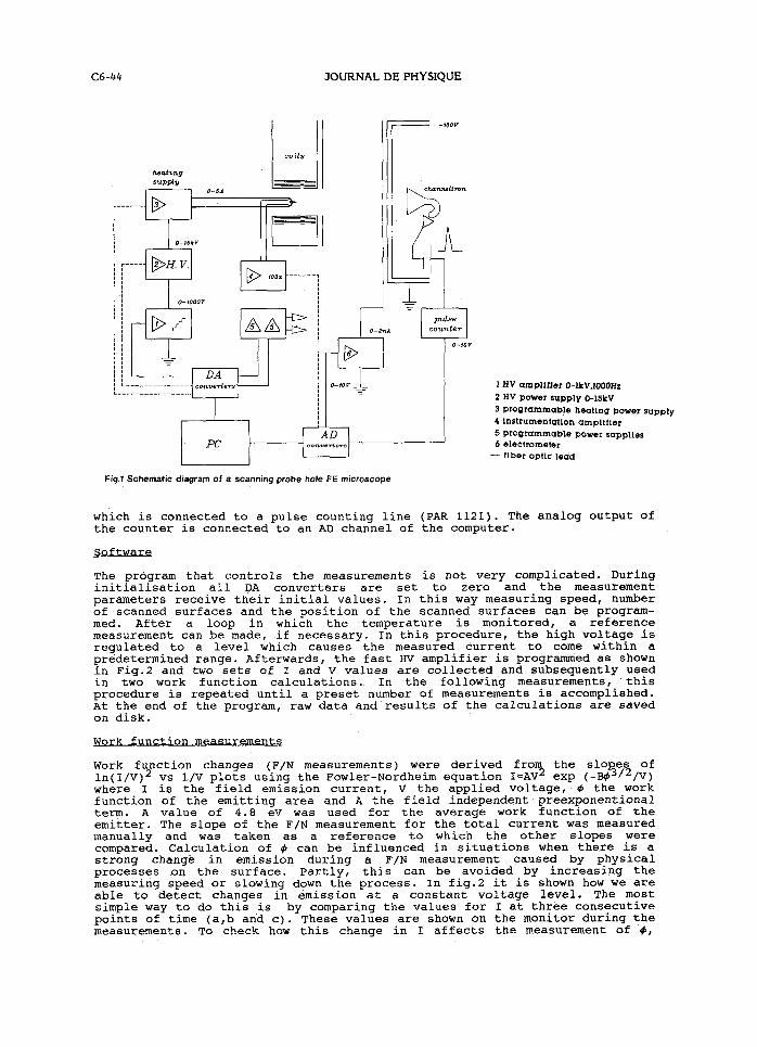
Hardware
The apparatus consists of a bakeable stainless steel UHV system with a base pressure in the 10-11 torr range, pumped by ion getter and titanium sub- limation pumps. Partial and total pressures are measured using respectively a quadrupole mass spectrometer and an ion gauge. The tip assembly is prepared as described elsewere [ 2 ] . Tip temperatures can be measured from 90K using a programmable current amplifier and an instrumentatron amplifier (resistance thermometry). The tip is surrounded by a grounded tube, which is part of a dewar reaching down from the top of the apparatus. It serves as an extracting lens for the field emitted electrons. Around the tube, 4 coils have been mounted to supply a variable quadrupole magnetic field. Two programmable current amplifiers are used as power supplies for the coils. A phosphor screen is placed in front of the tip. A probe hole in the center of the screen is followed by a channeltron electron multiplier. In order to suppress secondary electron emission from the screen and in the channeltron set up, retarding shields are held on a potential of -100V. In this way the stability of the total current, measured with Keithley 412 electrometer, is better than 2 PA. A schematic diagram of the field emission microscope is shown in fig.1. An Intel 8086 based computer is connected to the equipment by AD and DA converters. Two cascaded programmable high voltage amplifiers are used. The first one (0-1000V,1000Hz) enables to perform fast F/N measurements. The second one (Brandenburg aII) is used to reach a voltage level which causes sufficient electron emission from the tip. The program input of the Branden- burg amplifier is connected to the DA converter by a fiber optic connection. The detection part consists of a channeltron electron multiplier,
Article published online by EDP Sciences and available at http://dx.doi.org/10.1051/jphyscol:1988608
JOURNAL DE PHYSIQUE
coi l s
1 HV amplifier 0-lkV.1000Hz 2 Hv Dower supply 0-15kv 3 Programmable heating power supply 4 instrumentation amplilier 5 Programmable power supplies 6 electrometer
-- fiber optic lead
Fig.1 Schematic diagram of a scanning probe hole FE microscope
which is connected to a pulse counting line (PAR 1121). The analog output of the counter is connected to an AD channel of the computer.
Software
The program that controls the measurements is not very complicated. During initialisation all DA converters are set to zero and the measurement parameters receive their initial values. In this way measuring speed, number of scanned surfaces and the position of the scanned surfaces can be program- med. After a loop in which the temperature is monitored, a reference measurement can be made, if necessary. In this procedure, the high voltage is regulated to a level which causes the measured current to come within a predetermined range. Afterwards, the fast HV amplifier is programmed as shown in Fig.2 and two sets of I and V values are collected and subsequently used in two work function calculations. In the following measurements, this procedure is repeated until a preset number of measurements is accomplished. At the end of the program, raw data and results of the calculations are saved on disk.
function measurements
Work function changes (F/N measurements) were derived from the slo es of I~(I/v) vs 1/V plots using the Fowler-Nordheim equation I=AV~ exp ( -E38l2/V) where I is the field emission current, V the applied voltage, 4 the work function of the emitting area and A the field independent preexponentional term. A value of 4.8 eV was used for the average work function of the emitter. The slope of the F/N measurement for the total current was measured manually and was taken as a reference to which the other slopes were compared. Calculation of 4 can be influenced in situations when there is a strong change in emission during a F/N measurement caused by physical processes on the surface. Partly, this can be avoided by increasing the measuring speed or slowing down the process. In fig.2 it is shown how we are able to detect changes in emission at a constant voltage level. The most simple way to do this is by comparing the values for I at three consecutive points of time (a,b and c). These values are shown on the monitor during the measurements. To check how this change in I affects the measurement of +,
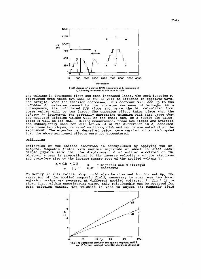
I 1.1 &--- 0 500 1000 1500 2000 2500 3000 3500 4000
Time (mSec)
Fig.2 Change of V during 1:FIN measurement 2: regulation of V, following deflect~on to the next surface
the voltage is decreased first and then increased later. The work function $, calculated from these two sets of values will be affected in opposite ways. For example, when the emission decreases, this decrease will add up to the decrease of emission caused by the stepwise decrease in voltage. As a consequence, the calculated F/N slope and hence the 64, calculated from these values will be too large. The opposite effect takes place when the voltage is increased. The gradually decreasing emission will then cause that the measured emission values will be too small and, as a result the calcu- lated 6$ will be too small. During measurement, these two slopes are averaged and subsequently used for calculation of 6$ The difference in $, obtained from these two slopes, is saved on floppy disk and can be evaluated after the experiment. The experiments, described below, were carried out at such speed that the above mentioned effects were not encountered.
Deflection of the emitted electrons is accomplished by applying two or- thogonal magnetic fields with maximum magnitude of about 15 Gauss each. Simple physics show that the displacement d of emitted electrons on the phosphor screen is proportional to the inverse velocity v of the electrons and therefore also to the inverse square root of the applied voltage V.
= 2 LB B = magnetic field sttength v C,C' = constants
To verify if this relationship could also be observed for our set up, the variation of the applied magnetic field, necessary to scan over two local emission maxima was measured at different applied voltages. In fig.3 it is shown that, within experimental error, this relationship can be observed for both emission maxima. The relation is used to adjust the magnetic field
. . 0 20 4 0 60 80 100 Fig.3 The correlation between the applied magnetic field B
and V for two constant deflection distances dl and 62
C6-46 JOURNAL DE PHYSIQUE
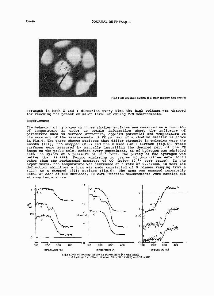
Fig.4 Field emission pattern of a clean rhodium field emitter
strength in both X and Y direction every time the high voltage was changed for reaching the preset emission level or during F/N measurements.
The behavior of hydrogen on three rhodium surfaces was measured as a function of temperature in order to obtain information about the influence of parameters such as surface structure, applied potential and temperature on the accuracy of the measurements. A FE pattern of a rhodium emitter is shown in Fig.4. The three chosen surfaces that differ strongly in emission were the smooth (Ill), the stepped (211) and the kinked (321) surface (fig.5). These surfaces were measured by manually installing the desired part of the FE image on the probe hole. Before every experiment, 5L of hydrogen was admitted into the system at a pressure of torr. The purity of the hydrogen was better than 99.999%. During admission no traces of impurities were found other than the background pressure of CO (below 10-l2 torr range). In the experiments, the temperature was increased at a rate of 0.2K/sec. To test the deflection abilities a scan was made consisting of 5 planes ranging from a (111) to a stepped (211) surface (fig.6). The area was scanned repeatedly until of each of the surfaces, 80 work function measurements were carried out at room temperature.
J t - .; 3 % ~
A 1 . J -
1
I 1 - h. F - 1 - i .
- Y A 2 0
"t L...... .- :
*. L. .. L.....
10 -
0.5 -
0
'-.:.
100 200 300 400 100 200 300 400 100 200 300 400
Temperature (K) Temperature (K) Temperature (K)
Fig.5 Ettect of heating on the FE parameters @,v and In(A) of 3 hydrogen covered surfaces: A:Rh(lll).B:Rh(211) andC:Rh(321).
-7
.? (kvolts) In(A) c .p&-r. : . . - . c \ \ ; C. : B i
': : L '? i 9 - , ni+...1(c ; '.-
L c . a
1 8 * , -37s
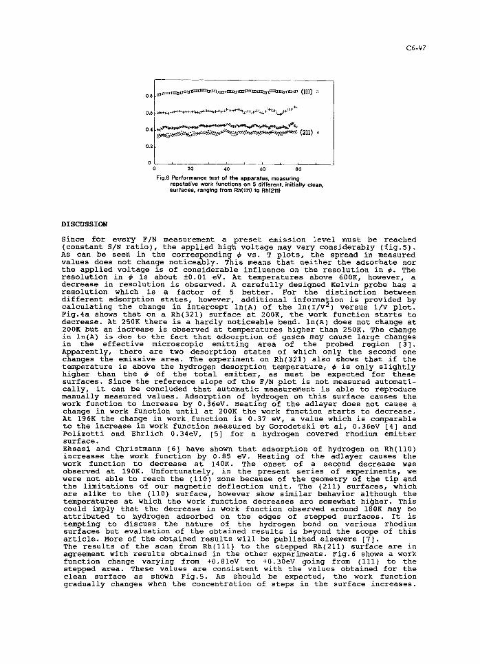
Fig.6 Performance test of the apparatus, measuring repetative work functions on 5 different, initially clean, surfaces, ranging from Rh(ll1) to Rh(211)
DISCUSSION
Since for every F/N measurement a preset emission level must be reached (constant S/N ratio), the applied high voltage may vary considerably (fig.5). As can be seen in the corresponding 6 vs. T plots, the spread in measured values does not change noticeably. This means that neither the adsorbate nor the applied voltage is of considerable influence on the resolution in #. The resolution in 6 is about k0.01 eV. At temperatures above 600K, however, a decrease in resolution is observed. A carefully designed Kelvin probe has a resolution which is a factor of 5 better. For the distinction between different adsorption states, however, additional information is provided by calculating the change in intercept ln(A) of the 1n(1/v2) versus 1/V plot. Fig.4a shows that on a Rh(321) surface at 200K, the work function starts to decrease. At 250K there is a hardly noticeable bend. ln(A) does not change at 200K but an increase is observed at temperatures higher than 250K. The change in ln(A) is due to the fact that adsorption of gases may cause large changes in the effective microscopic emitting area of the probed region [3]. Apparently, there are two desorption states of which only the second one changes the emissive area. The experiment on Rh(321) also shows that if the temperature is above the hydrogen desorption temperature, 6 is only slightly higher than the 9 of the total emitter, as must be expected for these surfaces. Since the reference slope of the F/N plot is not measured automati- cally, it can be concluded that automatic measurement is able to reproduce manually measured values. Adsorption of hydrogen on this surface causes the work function to increase by 0.36eV. Heating of the adlayer does not cause a change in work function until at 200K the work function starts to decrease. At 196K the change in work function is 0.37 eV, a value which is comparable to the increase in work function measured by Gorodetski et al, 0.36eV [4] and Polizotti and Ehrlich 0.34eV, [5] for a hydrogen covered rhodium emitter surface. Ehsasi and Christmann [6] have shown that adsorption of hydrogen on Rh(ll0) increases the work function by 0.85 eV. Heating of the adlayer causes the work function to decrease at 140K. The onset of a second decrease was observed at 190K. Unfortunately, in the present series of experiments, we were not able to reach the (110) zone because of the geometry of the tip and the limitations of our magnetic deflection unit. The (211) surfaces, which are alike to the (110) surface, however show similar behavior although the temperatures at which the work function decreases are somewhat hibher. This could imply that the decrease in work function observed around 180K may be attributed to hydrogen adsorbed on the edges of stepped surfaces. It is tempting to discuss the nature of the hydrogen bond on various rhodium surfaces but evaluation of the obtained results is beyond the scope of this article. More of the obtgined results will be published elsewere [7]. The results of the scan from Rh(ll1) to the stepped Rh(211) surface are in agreement with results obtained in the other experiments. Fig.6 shows a work function change varying from +0.81eV to +0.30eV going from (111) to the stepped area. These values are consistent with the values obtained for the clean surface as shown Fig.5. As should be expected, the work function gradually changes when the concentration of steps in the surface increases.
C6-48 JOURNAL DE PHYSIQUE
Moreover, the 6+ of 0.81eV, obtained for Rh(ll1) is comparable to Pt(ll1) which has a work function of 6.leV 181, which is 0.8eV higher than + for the total emitter. For Ir, the reported 6+ between Ir(ll1) and the total emitter is 0.7 eV [9].
CONCLUSIONS
Automation of a probe hole field emission microscope improves thcmanageabil- ity of this apparatus considerably. Deflection of the emitted electrons by means of a variable magnetic field was found to be dependent on the applied voltage which is in agreement with theory. Scanning of the field emission pattern across a probe hole enables experiments in which the influence of step densities upon surface phenomena can be studied.
The authors would like to thank R.van Schie and Y.Rijneveen for their help and suggestions in the construction of the scanning probe hole FE microscope.
REFERENCES
[I] V.V.Gorodetskii,B.E.NieuwenhuysrW.M.H.Sachtler and G.K.Boreskov, Appl.Surf.Sci.7(1981) 355, and references therein 121 H.A.C.M.Hehdrickx,A.M.E.Winkelman and B.E.Nieuwenhuys, Appl.Surf.S~:27 (1987) 458 and references therein
[3] R.Gomer, Harvard monographs in appl.sc.No.9, Harvard University Press, Carnbridge,Massachusetts 1961
[4] V.V.Gorodetski,B.E.Nieuwenhuys,W.M.H.Sachtler and G.K.Boreskov, Surf.Sc. 108(1981) 225-234
[5] R.S.Polizzotti ang G.Ehrlich, J.Chem.Phys.71(1979) 259 [6] M.Ehsasi and K.Christmann, Surf.Sci.194(1988) 172 [7] To be published [8] B.E.Nieuwenhuys, Surf.Sci.59(1976) 430 [9] B.E.Nieuwenhuys,D.T.Meyer and W.M.H.Sachtler, Surf.Sci.40(1973) 125