
16-Bit, 1600 MSPS, TxDAC+ Digital-to- Analog Converter ...€¦ · 16-Bit, 1600 MSPS, TxDAC+...
56
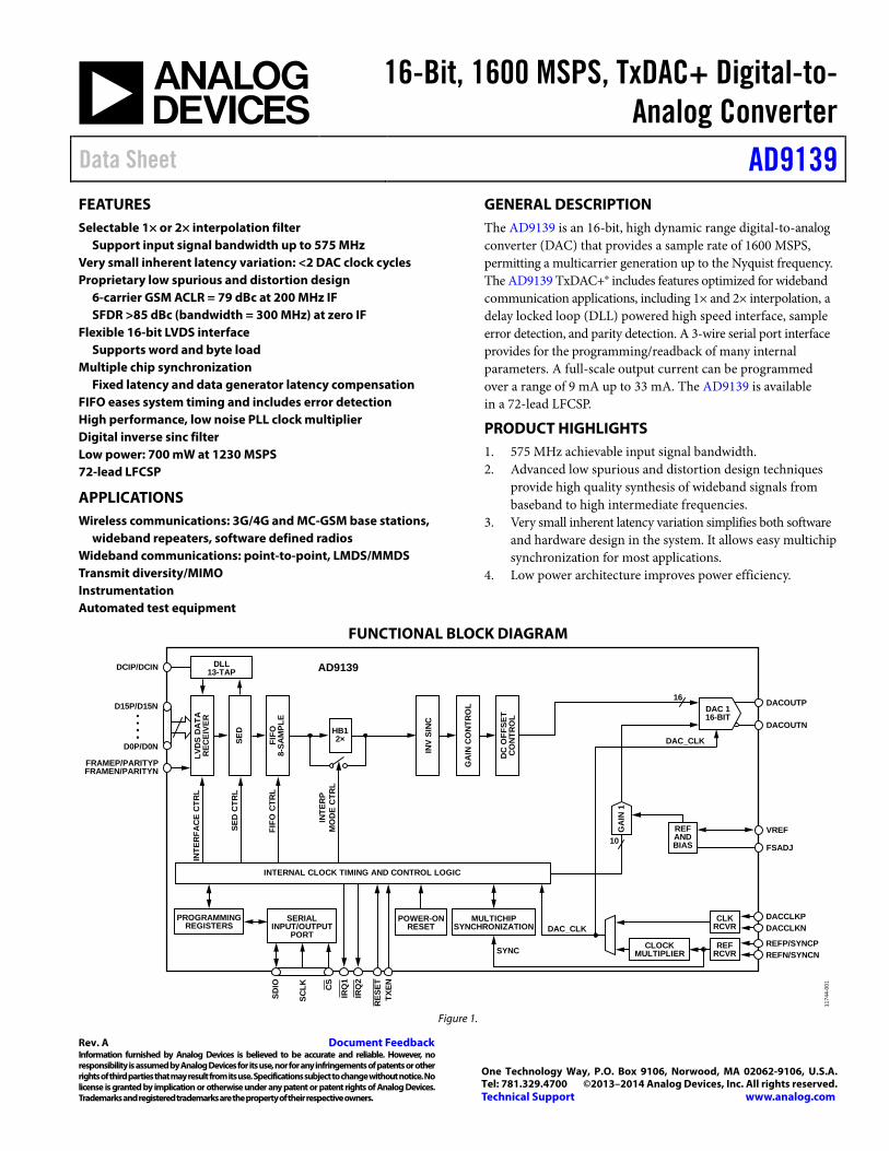
16-Bit, 1600 MSPS, TxDAC+ Digital-to- Analog Converter Data Sheet AD9139 FEATURES Selectable 1× or 2× interpolation filter Support input signal bandwidth up to 575 MHz Very small inherent latency variation: <2 DAC clock cycles Proprietary low spurious and distortion design 6-carrier GSM ACLR = 79 dBc at 200 MHz IF SFDR >85 dBc (bandwidth = 300 MHz) at zero IF Flexible 16-bit LVDS interface Supports word and byte load Multiple chip synchronization Fixed latency and data generator latency compensation FIFO eases system timing and includes error detection High performance, low noise PLL clock multiplier Digital inverse sinc filter Low power: 700 mW at 1230 MSPS 72-lead LFCSP APPLICATIONS Wireless communications: 3G/4G and MC-GSM base stations, wideband repeaters, software defined radios Wideband communications: point-to-point, LMDS/MMDS Transmit diversity/MIMO Instrumentation Automated test equipment GENERAL DESCRIPTION The AD9139 is an 16-bit, high dynamic range digital-to-analog converter (DAC) that provides a sample rate of 1600 MSPS, permitting a multicarrier generation up to the Nyquist frequency. The AD9139 TxDAC+® includes features optimized for wideband communication applications, including 1× and 2× interpolation, a delay locked loop (DLL) powered high speed interface, sample error detection, and parity detection. A 3-wire serial port interface provides for the programming/readback of many internal parameters. A full-scale output current can be programmed over a range of 9 mA up to 33 mA. The AD9139 is available in a 72-lead LFCSP. PRODUCT HIGHLIGHTS 1. 575 MHz achievable input signal bandwidth. 2. Advanced low spurious and distortion design techniques provide high quality synthesis of wideband signals from baseband to high intermediate frequencies. 3. Very small inherent latency variation simplifies both software and hardware design in the system. It allows easy multichip synchronization for most applications. 4. Low power architecture improves power efficiency. FUNCTIONAL BLOCK DIAGRAM Figure 1. REF AND BIAS FSADJ VREF POWER-ON RESET MULTICHIP SYNCHRONIZATION SERIAL INPUT/OUTPUT PORT PROGRAMMING REGISTERS SDIO SCLK CS RESET TXEN IRQ1 IRQ2 DACCLKP DACCLKN REFP/SYNCP REFN/SYNCN CLOCK MULTIPLIER CLK RCVR REF RCVR DAC_CLK LVDS DATA RECEIVER SED DLL 13-TAP D15P/D15N D0P/D0N FRAMEP/PARITYP FRAMEN/PARITYN DCIP/DCIN INTERFACE CTRL SED CTRL FIFO 8-SAMPLE FIFO CTRL INTERP MODE CTRL HB1 2× INV SINC GAIN CONTROL DC OFFSET CONTROL DAC 1 16-BIT DACOUTP DACOUTN 16 10 GAIN 1 INTERNAL CLOCK TIMING AND CONTROL LOGIC DAC_CLK SYNC AD9139 11744-001 Rev. A Document Feedback Information furnished by Analog Devices is believed to be accurate and reliable. However, no responsibility is assumed by Analog Devices for its use, nor for any infringements of patents or other rights of third parties that may result from its use. Specifications subject to change without notice. No license is granted by implication or otherwise under any patent or patent rights of Analog Devices. Trademarks and registered trademarks are the property of their respective owners. One Technology Way, P.O. Box 9106, Norwood, MA 02062-9106, U.S.A. Tel: 781.329.4700 ©2013–2014 Analog Devices, Inc. All rights reserved. Technical Support www.analog.com
Transcript of 16-Bit, 1600 MSPS, TxDAC+ Digital-to- Analog Converter ...€¦ · 16-Bit, 1600 MSPS, TxDAC+...
16-Bit, 1600 MSPS, TxDAC+ Digital-to-Analog Converter
Data Sheet AD9139
FEATURES Selectable 1× or 2× interpolation filter
Support input signal bandwidth up to 575 MHz Very small inherent latency variation: <2 DAC clock cycles Proprietary low spurious and distortion design
6-carrier GSM ACLR = 79 dBc at 200 MHz IF SFDR >85 dBc (bandwidth = 300 MHz) at zero IF
Flexible 16-bit LVDS interface Supports word and byte load
Multiple chip synchronization Fixed latency and data generator latency compensation
FIFO eases system timing and includes error detection High performance, low noise PLL clock multiplier Digital inverse sinc filter Low power: 700 mW at 1230 MSPS 72-lead LFCSP
APPLICATIONS Wireless communications: 3G/4G and MC-GSM base stations,
wideband repeaters, software defined radios Wideband communications: point-to-point, LMDS/MMDS Transmit diversity/MIMO Instrumentation Automated test equipment
GENERAL DESCRIPTION The AD9139 is an 16-bit, high dynamic range digital-to-analog converter (DAC) that provides a sample rate of 1600 MSPS, permitting a multicarrier generation up to the Nyquist frequency. The AD9139 TxDAC+® includes features optimized for wideband communication applications, including 1× and 2× interpolation, a delay locked loop (DLL) powered high speed interface, sample error detection, and parity detection. A 3-wire serial port interface provides for the programming/readback of many internal parameters. A full-scale output current can be programmed over a range of 9 mA up to 33 mA. The AD9139 is available in a 72-lead LFCSP.
PRODUCT HIGHLIGHTS 1. 575 MHz achievable input signal bandwidth. 2. Advanced low spurious and distortion design techniques
provide high quality synthesis of wideband signals from baseband to high intermediate frequencies.
3. Very small inherent latency variation simplifies both software and hardware design in the system. It allows easy multichip synchronization for most applications.
4. Low power architecture improves power efficiency.
FUNCTIONAL BLOCK DIAGRAM
Figure 1.
REFANDBIAS FSADJ
VREF
POWER-ONRESET
MULTICHIPSYNCHRONIZATION
SERIALINPUT/OUTPUT
PORT
PROGRAMMINGREGISTERS
SDIO
SCLK C
S
RES
ETTX
EN
IRQ
1IR
Q2
DACCLKPDACCLKN
REFP/SYNCPREFN/SYNCN
CLOCKMULTIPLIER
CLKRCVR
REFRCVR
DAC_CLK
LVD
S D
ATA
REC
EIVE
R
SED
DLL13-TAP
D15P/D15N
D0P/D0N
FRAMEP/PARITYPFRAMEN/PARITYN
DCIP/DCIN
INTE
RFA
CE
CTR
L
SED
CTR
L
FIFO
8-SA
MPL
EFI
FO C
TRL
INTE
RP
MO
DE
CTR
L
HB12×
INV
SIN
C
GA
IN C
ON
TRO
L
DC
OFF
SET
CO
NTR
OL
DAC 116-BIT
DACOUTP
DACOUTN
16
10
GA
IN 1
INTERNAL CLOCK TIMING AND CONTROL LOGIC
DAC_CLK
SYNC
AD9139
1174
4-00
1
Rev. A Document Feedback Information furnished by Analog Devices is believed to be accurate and reliable. However, no responsibility is assumed by Analog Devices for its use, nor for any infringements of patents or other rights of third parties that may result from its use. Specifications subject to change without notice. No license is granted by implication or otherwise under any patent or patent rights of Analog Devices. Trademarks and registered trademarks are the property of their respective owners.
One Technology Way, P.O. Box 9106, Norwood, MA 02062-9106, U.S.A. Tel: 781.329.4700 ©2013–2014 Analog Devices, Inc. All rights reserved. Technical Support www.analog.com

AD9139 Data Sheet
TABLE OF CONTENTS Features .............................................................................................. 1 Applications ....................................................................................... 1 General Description ......................................................................... 1 Product Highlights ........................................................................... 1 Functional Block Diagram .............................................................. 1 Revision History ............................................................................... 3 Specifications ..................................................................................... 4
DC Specifications ......................................................................... 4 Digital Specifications ................................................................... 5 Latency Variation Specifications ................................................ 6 AC Specifications .......................................................................... 6 Operating Speed Specifications .................................................. 6 Absolute Maximum Ratings ....................................................... 7 Thermal Resistance ...................................................................... 7 ESD Caution .................................................................................. 7
Pin Configuration and Function Descriptions ............................. 8 Typical Performance Characteristics ........................................... 11 Terminology .................................................................................... 15 Serial Port Operation ..................................................................... 16
Data Format ................................................................................ 16 Serial Port Pin Descriptions ...................................................... 16 Serial Port Options ..................................................................... 16
Data Interface .................................................................................. 18 LVDS Input Data Ports .............................................................. 18 Word Interface Mode ................................................................. 18 Byte Interface Mode ................................................................... 18 Data Interface Configuration Options .................................... 18 DLL Interface Mode ................................................................... 18 Parity ............................................................................................ 21 SED Operation ............................................................................ 21 SED Example ............................................................................... 22 Delay Line Interface Mode ........................................................ 22
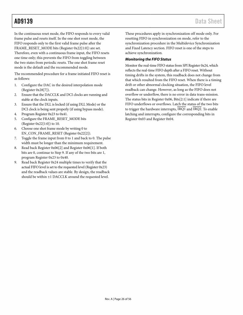
FIFO Operation .............................................................................. 24 Resetting the FIFO ..................................................................... 25 Serial Port Initiated FIFO Reset ............................................... 25 Frame Initiated FIFO Reset ....................................................... 25
Digital Datapath .............................................................................. 27 Interpolation Filters ................................................................... 27 Inverse Sinc Filter ....................................................................... 28 Digital Function Configuration ................................................ 28
Multidevice Synchronization and Fixed Latency ....................... 29 Very Small Inherent Latency Variation ................................... 29 Further Reducing the Latency Variation ................................. 29 Synchronization Implementation ............................................ 29 Synchronization Procedures ..................................................... 30
Interrupt Request Operation ........................................................ 32 Interrupt Working Mechanism ................................................ 32 Interrupt Service Routine .......................................................... 32
Temperature Sensor ....................................................................... 33 DAC Input Clock Configurations ................................................ 34
Driving the DACCLK and REFCLK Inputs ........................... 34 Direct Clocking .......................................................................... 34 Clock Multiplication .................................................................. 34 PLL Settings ................................................................................ 35 Configuring the VCO Tuning Band ........................................ 35 Automatic VCO Band Select .................................................... 35 Manual VCO Band Select ......................................................... 35 PLL Enable Sequence ................................................................. 35
Analog Outputs............................................................................... 36 Transmit DAC Operation .......................................................... 36 Interfacing to Modulators ......................................................... 37 Reducing LO Leakage and Unwanted Sidebands .................. 38
Start-Up Routine ............................................................................ 39 Device Configuration Register Map and Description ............... 40
SPI Configure Register .............................................................. 42 Power-Down Control Register ................................................. 42 Interrupt Enable 0 Register ....................................................... 42 Interrupt Enable 1 Register ....................................................... 42 Interrupt Flag 0 Register ............................................................ 43 Interrupt Flag 1 Register ............................................................ 43 Interrupt Select 0 Register ......................................................... 43 Interrupt Select 1 Register ......................................................... 44 Frame Mode Register ................................................................. 44 Data Control 0 Register ............................................................. 44 Data Control 1 Register ............................................................. 44 Data Control 2 Register ............................................................. 45 Data Control 3 Register ............................................................. 45 Data Status 0 Register ................................................................ 45 DAC Clock Receiver Control Register .................................... 46 Reference Clock Receiver Control Register ............................ 46
Rev. A | Page 2 of 56
Data Sheet AD9139
PLL Control Register .................................................................. 46 PLL Control Register .................................................................. 47 PLL Control Register .................................................................. 47 PLL Status Register ..................................................................... 47 PLL Status Register ..................................................................... 48 DAC FS Adjust LSB Register ..................................................... 48 DAC FS Adjust MSB Register .................................................... 48 Die Temperature Sensor Control Register ............................... 48 Die Temperature LSB Register .................................................. 48 Die Temperature MSB Register ................................................. 49 Chip ID Register .......................................................................... 49 Interrupt Configuration Register .............................................. 49 Sync CTRL Register .................................................................... 49 Frame Reset CTRL Register ....................................................... 49 FIFO Level Configuration Register .......................................... 50 FIFO Level Readback Register .................................................. 50 FIFO CTRL Register ................................................................... 50 Data Format Select Register ....................................................... 51 Datapath Control Register ......................................................... 51 Interpolation Control Register .................................................. 51 Power-Down Data Input 0 Register.......................................... 51 DAC_DC_OFFSET0 Register ................................................... 51 DAC_DC_OFFSET1 Register ................................................... 51 DAC_GAIN_ADJ Register ........................................................ 52
Gain Step Control0 Register ...................................................... 52 Gain Step Control1 Register ...................................................... 52 TX Enable Control Register ...................................................... 52 DAC Output Control Register .................................................. 53 DLL Cell Enable 0 Register ........................................................ 53 DLL Cell Enable 1 Register ........................................................ 53 SED Control Register ................................................................. 53 SED Pattern S0 Low Bits Register ............................................. 54 SED Pattern S0 High Bits Register ............................................ 54 SED Pattern S1 Low Bits Register ............................................. 54 SED Pattern S1 High Bits Register ............................................ 54 SED Pattern S2 Low Bits Register ............................................. 54 SED Pattern S2 High Bits Register ............................................ 54 SED Pattern S3 Low Bits Register ............................................. 54 SED Pattern S3 High Bits Register ............................................ 55 Parity Control Register ............................................................... 55 Parity Error Rising Edge Register ............................................. 55 Parity Error Falling Edge Register ............................................ 55 Version Register .......................................................................... 55
Packaging and Ordering Information .......................................... 56 Outline Dimensions ................................................................... 56 Ordering Guide ........................................................................... 56
REVISION HISTORY 3/14—Rev. 0 to Rev. A
Change to Register 0x7F, Table 21................................................. 41 Change to Table 80 .......................................................................... 55
10/13—Revision 0: Initial Version
Rev. A | Page 3 of 56

AD9139 Data Sheet
SPECIFICATIONS DC SPECIFICATIONS TMIN to TMAX, AVDD33 = 3.3 V, DVDD18 = 1.8 V, CVDD18 = 1.8 V, IOUTFS = 20 mA, maximum sample rate, unless otherwise noted.
Table 1. Parameter Test Conditions/Comments Min Typ Max Unit RESOLUTION 16 Bits ACCURACY
Differential Nonlinearity (DNL) ±2.1 LSB Integral Nonlinearity (INL) ±3.7 LSB
MAIN DAC OUTPUT Offset Error −0.001 0 +0.001 % FSR Gain Error With internal reference −3.2 +2 +4.7 % FSR Full-Scale Output Current 10 kΩ external resistor between FSADJ and AVSS 19.06 19.8 20.6 mA Output Compliance Range −1.0 +1.0 V Output Resistance 10 MΩ Gain DAC Monotonicity Guaranteed Settling Time to Within ±0.5 LSB 20 ns
MAIN DAC TEMPERATURE DRIFT Offset 0.04 ppm/°C Gain 100 ppm/°C Reference Voltage 30 ppm/°C
REFERENCE Internal Reference Voltage 1.17 1.19 V Output Resistance 5 kΩ
ANALOG SUPPLY VOLTAGES AVDD33 3.13 3.3 3.47 V CVDD18 1.7 1.8 1.9 V
DIGITAL SUPPLY VOLTAGES DVDD18 1.7 1.8 1.9 V
DVDD18 Variation over Operating Conditions1
−2.5% +2.5% V
POWER CONSUMPTION 1× Mode fDAC = 614 MSPS 440 mW fDAC = 1230 MSPS 700 mW 2× Mode fDAC = 800 MSPS 670 mW fDAC = 1600 MSPS 1150 mW Phase-Locked Loop 70 mW Inverse Sinc fDAC = 1230 MSPS 60 mW Reduced Power Mode (Power-Down) 57.3 mW AVDD33 Current 0.4 mA CVDD18 Current 26.6 mA DVDD18 Current 4.5 mA
OPERATING RANGE −40 +25 +85 °C
1 This parameter specifies the maximum allowable variation of DVDD18 over operating conditions compared with the DVDD18 presented to the device at the time the data interface DLL is enabled.
Rev. A | Page 4 of 56
Data Sheet AD9139
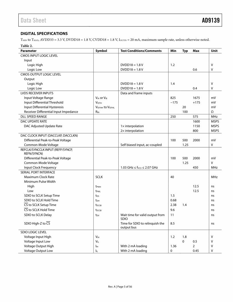
DIGITAL SPECIFICATIONS TMIN to TMAX, AVDD33 = 3.3 V, DVDD18 = 1.8 V, CVDD18 = 1.8 V, IOUTFS = 20 mA, maximum sample rate, unless otherwise noted.
Table 2. Parameter Symbol Test Conditions/Comments Min Typ Max Unit CMOS INPUT LOGIC LEVEL
Input Logic High DVDD18 = 1.8 V 1.2 V Logic Low DVDD18 = 1.8 V 0.6 V
CMOS OUTPUT LOGIC LEVEL Output
Logic High DVDD18 = 1.8 V 1.4 V Logic Low DVDD18 = 1.8 V 0.4 V
LVDS RECEIVER INPUTS Data and frame inputs Input Voltage Range VIA or VIB 825 1675 mV Input Differential Threshold VIDTH −175 +175 mV Input Differential Hysteresis VIDTHH to VIDTHL 20 mV Receiver Differential Input Impedance RIN 100 Ω
DLL SPEED RANGE 250 575 MHz DAC UPDATE RATE 1600 MSPS
DAC Adjusted Update Rate 1× interpolation 1150 MSPS 2× interpolation 800 MSPS DAC CLOCK INPUT (DACCLKP, DACCLKN)
Differential Peak-to-Peak Voltage 100 500 2000 mV Common-Mode Voltage Self biased input, ac-coupled 1.25 V
REFCLK/SYNCCLK INPUT (REFP/SYNCP, REFN/SYNCN)
Differential Peak-to-Peak Voltage 100 500 2000 mV Common-Mode Voltage 1.25 V Input Clock Frequency 1.03 GHz ≤ fVCO ≤ 2.07 GHz 450 MHz
SERIAL PORT INTERFACE Maximum Clock Rate SCLK 40 MHz Minimum Pulse Width
High tPWH 12.5 ns Low tPWL 12.5 ns
SDIO to SCLK Setup Time tDS 1.5 ns SDIO to SCLK Hold Time tDH 0.68 ns CS to SCLK Setup Time tDCSB 2.38 1.4 ns
CS to SCLK Hold Time tDCSB 9.6 ns
SDIO to SCLK Delay tDV Wait time for valid output from SDIO
11 ns
SDIO High-Z to CS Time for SDIO to relinquish the output bus
8.5 ns
SDIO LOGIC LEVEL Voltage Input High VIH 1.2 1.8 V Voltage Input Low VIL 0 0.5 V Voltage Output High IIH With 2 mA loading 1.36 2 V Voltage Output Low IIL With 2 mA loading 0 0.45 V
Rev. A | Page 5 of 56
AD9139 Data Sheet
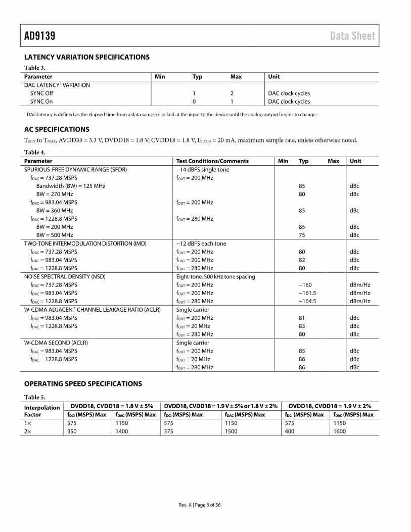
LATENCY VARIATION SPECIFICATIONS Table 3. Parameter Min Typ Max Unit DAC LATENCY1 VARIATION
SYNC Off 1 2 DAC clock cycles SYNC On 0 1 DAC clock cycles
1 DAC latency is defined as the elapsed time from a data sample clocked at the input to the device until the analog output begins to change.
AC SPECIFICATIONS TMIN to TMAX, AVDD33 = 3.3 V, DVDD18 = 1.8 V, CVDD18 = 1.8 V, IOUTFS = 20 mA, maximum sample rate, unless otherwise noted.
Table 4. Parameter Test Conditions/Comments Min Typ Max Unit SPURIOUS-FREE DYNAMIC RANGE (SFDR) −14 dBFS single tone
fDAC = 737.28 MSPS fOUT = 200 MHz Bandwidth (BW) = 125 MHz 85 dBc BW = 270 MHz 80 dBc
fDAC = 983.04 MSPS fOUT = 200 MHz BW = 360 MHz 85 dBc
fDAC = 1228.8 MSPS fOUT = 280 MHz BW = 200 MHz 85 dBc BW = 500 MHz 75 dBc
TWO-TONE INTERMODULATION DISTORTION (IMD) −12 dBFS each tone fDAC = 737.28 MSPS fOUT = 200 MHz 80 dBc fDAC = 983.04 MSPS fOUT = 200 MHz 82 dBc fDAC = 1228.8 MSPS fOUT = 280 MHz 80 dBc
NOISE SPECTRAL DENSITY (NSD) Eight-tone, 500 kHz tone spacing fDAC = 737.28 MSPS fOUT = 200 MHz −160 dBm/Hz fDAC = 983.04 MSPS fOUT = 200 MHz −161.5 dBm/Hz fDAC = 1228.8 MSPS fOUT = 280 MHz −164.5 dBm/Hz
W-CDMA ADJACENT CHANNEL LEAKAGE RATIO (ACLR) Single carrier fDAC = 983.04 MSPS fOUT = 200 MHz 81 dBc fDAC = 1228.8 MSPS fOUT = 20 MHz 83 dBc fOUT = 280 MHz 80 dBc
W-CDMA SECOND (ACLR) Single carrier fDAC = 983.04 MSPS fOUT = 200 MHz 85 dBc fDAC = 1228.8 MSPS fOUT = 20 MHz 86 dBc fOUT = 280 MHz 86 dBc
OPERATING SPEED SPECIFICATIONS
Table 5.
Interpolation Factor
DVDD18, CVDD18 = 1.8 V ± 5% DVDD18, CVDD18 = 1.9 V ± 5% or 1.8 V ± 2% DVDD18, CVDD18 = 1.9 V ± 2% fDCI (MSPS) Max fDAC (MSPS) Max fDCI (MSPS) Max fDAC (MSPS) Max fDCI (MSPS) Max fDAC (MSPS) Max
1× 575 1150 575 1150 575 1150 2× 350 1400 375 1500 400 1600
Rev. A | Page 6 of 56
Data Sheet AD9139
ABSOLUTE MAXIMUM RATINGS Table 6. Parameter Rating AVDD33 to GND −0.3 V to +3.6 V DVDD18, CVDD18 to GND −0.3 V to +2.1 V FSADJ, VREF, DACOUTP/DACOUTN, to
GND −0.3 V to AVDD33 + 0.3 V
D15P to D0P/D15N to D0N, FRAMEP/FRAMEN, DCIP/DCIN to GND
−0.3 V to DVDD18 + 0.3 V
DACCLKP/DACCLKN, REFP/SYNCP/REFN/SYNCN to GND
−0.3 V to CVDD18 + 0.3 V
RESET, IRQ1, IRQ2, CS, SCLK, SDIO to GND
−0.3 V to DVDD18 + 0.3 V
Junction Temperature 125°C Storage Temperature Range −65°C to +150°C
THERMAL RESISTANCE The exposed pad (EPAD) must be soldered to the ground plane (AVSS) for the 72-lead LFCSP. The EPAD provides an electrical, thermal, and mechanical connection to the board.
Typical θJA, θJB, and θJC values are specified for a 4-layer board in still air. Airflow increases heat dissipation, effectively reducing θJA and θJB.
Table 7. Thermal Resistance Package θJA θJB θJC Unit Conditions 72-Lead LFCSP 20.7 10.9 1.1 °C/W EPAD soldered
to ground plane
ESD CAUTION
Stresses above those listed under Absolute Maximum Ratingsmay cause permanent damage to the device. This is a stressrating only; functional operation of the device at these or anyother conditions above those indicated in the operationalsection of this specification is not implied. Exposure to absolutemaximum rating conditions for extended periods may affectdevice reliability.
Rev. A | Page 7 of 56
AD9139 Data Sheet
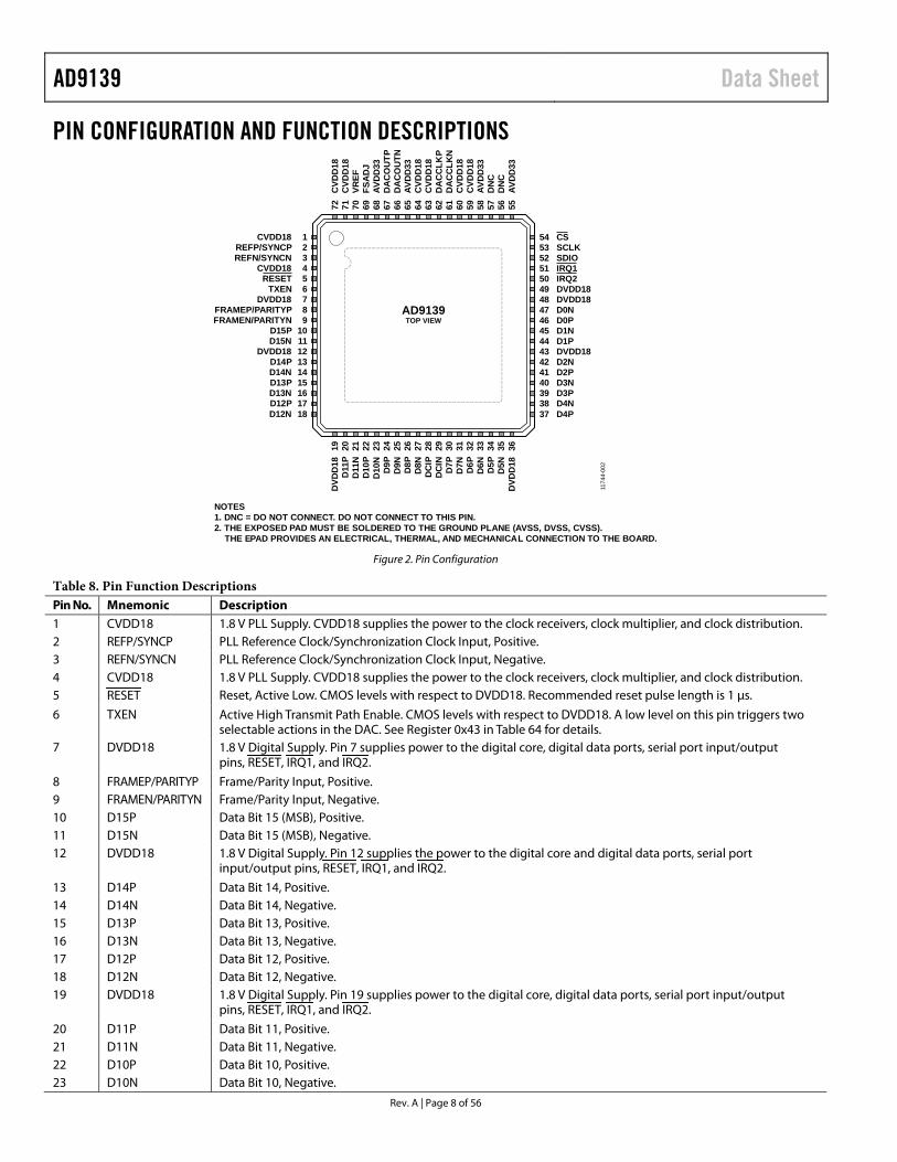
PIN CONFIGURATION AND FUNCTION DESCRIPTIONS
Figure 2. Pin Configuration
Table 8. Pin Function Descriptions Pin No. Mnemonic Description 1 CVDD18 1.8 V PLL Supply. CVDD18 supplies the power to the clock receivers, clock multiplier, and clock distribution. 2 REFP/SYNCP PLL Reference Clock/Synchronization Clock Input, Positive. 3 REFN/SYNCN PLL Reference Clock/Synchronization Clock Input, Negative. 4 CVDD18 1.8 V PLL Supply. CVDD18 supplies the power to the clock receivers, clock multiplier, and clock distribution. 5 RESET Reset, Active Low. CMOS levels with respect to DVDD18. Recommended reset pulse length is 1 µs.
6 TXEN Active High Transmit Path Enable. CMOS levels with respect to DVDD18. A low level on this pin triggers two selectable actions in the DAC. See Register 0x43 in Table 64 for details.
7 DVDD18 1.8 V Digital Supply. Pin 7 supplies power to the digital core, digital data ports, serial port input/output pins, RESET, IRQ1, and IRQ2.
8 FRAMEP/PARITYP Frame/Parity Input, Positive. 9 FRAMEN/PARITYN Frame/Parity Input, Negative. 10 D15P Data Bit 15 (MSB), Positive. 11 D15N Data Bit 15 (MSB), Negative. 12 DVDD18 1.8 V Digital Supply. Pin 12 supplies the power to the digital core and digital data ports, serial port
input/output pins, RESET, IRQ1, and IRQ2.
13 D14P Data Bit 14, Positive. 14 D14N Data Bit 14, Negative. 15 D13P Data Bit 13, Positive. 16 D13N Data Bit 13, Negative. 17 D12P Data Bit 12, Positive. 18 D12N Data Bit 12, Negative. 19 DVDD18 1.8 V Digital Supply. Pin 19 supplies power to the digital core, digital data ports, serial port input/output
pins, RESET, IRQ1, and IRQ2.
20 D11P Data Bit 11, Positive. 21 D11N Data Bit 11, Negative. 22 D10P Data Bit 10, Positive. 23 D10N Data Bit 10, Negative.
123456789
10111213141516
CVDD18REFP/SYNCPREFN/SYNCN
CVDD18RESET
TXENDVDD18
FRAMEP/PARITYPFRAMEN/PARITYN
D15PD15N
DVDD18D14PD14ND13PD13N
17D12P18D12N
19 20 21 22 23 24 25 26 27 28 29 30 31 32 33 34
DVD
D18
D11
PD
11N
D10
PD
10N
D9P
D9N D8P
D8N
DC
IPD
CIN
D7P
D7N D6P
D6N D5P
35D
5N36
DVD
D18
545352515049484746454443424140393837
CSSCLKSDIOIRQ1IRQ2DVDD18DVDD18D0ND0PD1ND1PDVDD18D2ND2PD3ND3PD4ND4P
72 71 70 69 68 67 66 65 64 63 62 61 60 59 58 57 56 55
CVD
D18
CVD
D18
VREF
FSA
DJ
AVD
D33
DA
CO
UTP
DA
CO
UTN
AVD
D33
CVD
D18
CVD
D18
DA
CC
LKP
DA
CC
LKN
CVD
D18
CVD
D18
AVD
D33
DN
CD
NC
AVD
D33
NOTES1. DNC = DO NOT CONNECT. DO NOT CONNECT TO THIS PIN.2. THE EXPOSED PAD MUST BE SOLDERED TO THE GROUND PLANE (AVSS, DVSS, CVSS). THE EPAD PROVIDES AN ELECTRICAL, THERMAL, AND MECHANICAL CONNECTION TO THE BOARD.
1174
4-00
2
AD9139TOP VIEW
Rev. A | Page 8 of 56
Data Sheet AD9139
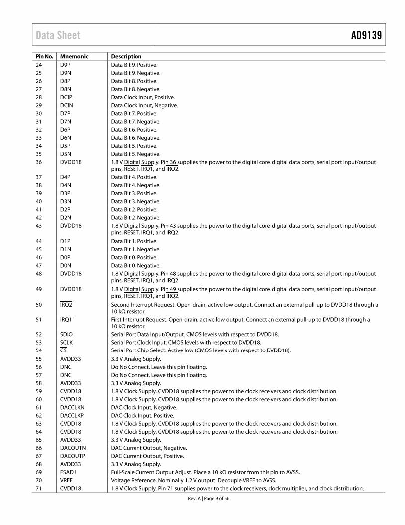
Pin No. Mnemonic Description 24 D9P Data Bit 9, Positive. 25 D9N Data Bit 9, Negative. 26 D8P Data Bit 8, Positive. 27 D8N Data Bit 8, Negative. 28 DCIP Data Clock Input, Positive. 29 DCIN Data Clock Input, Negative. 30 D7P Data Bit 7, Positive. 31 D7N Data Bit 7, Negative. 32 D6P Data Bit 6, Positive. 33 D6N Data Bit 6, Negative. 34 D5P Data Bit 5, Positive. 35 D5N Data Bit 5, Negative. 36 DVDD18 1.8 V Digital Supply. Pin 36 supplies the power to the digital core, digital data ports, serial port input/output
pins, RESET, IRQ1, and IRQ2.
37 D4P Data Bit 4, Positive. 38 D4N Data Bit 4, Negative. 39 D3P Data Bit 3, Positive. 40 D3N Data Bit 3, Negative. 41 D2P Data Bit 2, Positive. 42 D2N Data Bit 2, Negative. 43 DVDD18 1.8 V Digital Supply. Pin 43 supplies the power to the digital core, digital data ports, serial port input/output
pins, RESET, IRQ1, and IRQ2.
44 D1P Data Bit 1, Positive. 45 D1N Data Bit 1, Negative. 46 D0P Data Bit 0, Positive. 47 D0N Data Bit 0, Negative. 48 DVDD18 1.8 V Digital Supply. Pin 48 supplies the power to the digital core, digital data ports, serial port input/output
pins, RESET, IRQ1, and IRQ2.
49 DVDD18 1.8 V Digital Supply. Pin 49 supplies the power to the digital core, digital data ports, serial port input/output pins, RESET, IRQ1, and IRQ2.
50 IRQ2 Second Interrupt Request. Open-drain, active low output. Connect an external pull-up to DVDD18 through a 10 kΩ resistor.
51 IRQ1 First Interrupt Request. Open-drain, active low output. Connect an external pull-up to DVDD18 through a 10 kΩ resistor.
52 SDIO Serial Port Data Input/Output. CMOS levels with respect to DVDD18. 53 SCLK Serial Port Clock Input. CMOS levels with respect to DVDD18. 54 CS Serial Port Chip Select. Active low (CMOS levels with respect to DVDD18).
55 AVDD33 3.3 V Analog Supply. 56 DNC Do No Connect. Leave this pin floating. 57 DNC Do No Connect. Leave this pin floating. 58 AVDD33 3.3 V Analog Supply. 59 CVDD18 1.8 V Clock Supply. CVDD18 supplies the power to the clock receivers and clock distribution. 60 CVDD18 1.8 V Clock Supply. CVDD18 supplies the power to the clock receivers and clock distribution. 61 DACCLKN DAC Clock Input, Negative. 62 DACCLKP DAC Clock Input, Positive. 63 CVDD18 1.8 V Clock Supply. CVDD18 supplies the power to the clock receivers and clock distribution. 64 CVDD18 1.8 V Clock Supply. CVDD18 supplies the power to the clock receivers and clock distribution. 65 AVDD33 3.3 V Analog Supply. 66 DACOUTN DAC Current Output, Negative. 67 DACOUTP DAC Current Output, Positive. 68 AVDD33 3.3 V Analog Supply. 69 FSADJ Full-Scale Current Output Adjust. Place a 10 kΩ resistor from this pin to AVSS. 70 VREF Voltage Reference. Nominally 1.2 V output. Decouple VREF to AVSS. 71 CVDD18 1.8 V Clock Supply. Pin 71 supplies power to the clock receivers, clock multiplier, and clock distribution.
Rev. A | Page 9 of 56
AD9139 Data Sheet
Pin No. Mnemonic Description 72 CVDD18 1.8 V Clock Supply. Pin 72 supplies power to the clock receivers, clock multiplier, and clock distribution. EPAD Exposed Pad. The exposed pad (EPAD) must be soldered to the ground plane (AVSS, DVSS, CVSS). The EPAD
provides an electrical, thermal, and mechanical connection to the board.
Rev. A | Page 10 of 56

Data Sheet AD9139
TYPICAL PERFORMANCE CHARACTERISTICS
Figure 3. Single-Tone (0 dBFS) SFDR vs. fOUT in the First Nyquist Zone over fDAC
Figure 4. Single-Tone Second Harmonic vs. fOUT in the First Nyquist Zone
over Digital Back Off, fDAC = 1228.8 MHz
Figure 5. Single-Tone Third Harmonic vs. fOUT in the First Nyquist Zone
over Digital Back Off, fDAC = 1228.8 MHz
Figure 6. Single-Tone SFDR Excluding 2nd and 3rd Harmonics vs. fOUT in the
First Nyquist Zone over fDAC and Digital Back Off
Figure 7. Two-Tone Third IMD vs. fOUT over fDAC
Figure 8. Two-Tone Third IMD vs. fOUT over Digital Back Off,
fDAC = 1228.8 MHz
–40
–50
–60
–70
SFD
R (d
Bc)
–80
–90
–1000 100 200 300
fOUT (MHz)400 500 600
1174
4-00
3
700
fDAC = 737.28MHzfDAC = 983.04MHzfDAC = 1228.8MHz
–40
–50
–60
–70
SEC
ON
D H
AR
MO
NIC
(dB
c)
–80
–90
–1000 100 200 300
fOUT (MHz)400 500 600
1174
4-00
4
700
0dBFS–6dBFS–12dBFS–16dBFS
–40
–50
–60
–70
THIR
D H
AR
MO
NIC
(dB
c)
–80
–90
–1000 100 200 300
fOUT (MHz)400 500 600
1 174
4-00
5
700
0dBFS–6dBFS–12dBFS–16dBFS
–40
–50
–60
0dBFS–12dBFS
–70
SFD
R (d
Bc)
–80
–90
–1000 50 100 150
fOUT (MHz)200 250 300 350
1174
4-00
6
400
fDAC = 800MHzfDAC = 1600MHz
–40
–50
–60
–70
IMD
(dB
c)
–80
–90
–1000 100 200 300
fOUT (MHz)400 500 600
1174
4-00
8
700
fDAC = 737.28MHzfDAC = 983.04MHzfDAC = 1228.8MHz
–40
–50
–60
–70
IMD
(dB
c)
–80
–90
–1000 100 200 300 400 500 600
1174
4-00
9
700
0dBFS–6dBFS–12dBFS–16dBFS
fOUT (MHz)
Rev. A | Page 11 of 56

AD9139 Data Sheet
Figure 9. Two-Tone Third IMD vs. fOUT over PLL on and off,
fDAC = 1228.8 MHz
Figure 10. Single-Tone (0 dBFS) NSD vs. fOUT over fDAC
Figure 11. Single-Tone NSD vs. fOUT, over Digital Back Off, fDAC = 1228.8 MHz
Figure 12. Single-Tone NSD vs. fOUT, over Digital Back Off, PLL on and off
Figure 13. 1-Carrier WCDMA 1st Adjacent ACLR vs. fOUT over fDAC
PLL on and off
Figure 14. 1-Carrier WCDMA 2nd Adjacent ACLR vs. fOUT over fDAC
PLL on and off
–40
–50
–60
–70
IMD
(dB
c)
–80
–90
–1000 100 200 300 400 500 600 700
PLL OFFPLL ON
1 174
4-01
0
fOUT (MHz)
–145
–150
–155
NSD
(dB
m/H
z)
–160
–165
–1700 100 200 300
fOUT (MHz)400 500 600
1174
4-01
1
700
fDAC = 737.28MHzfDAC = 983.04MHzfDAC = 1228.8MHz
–150
–155
–160
–165
NSD
(dB
m/H
z)
–1700 100 200 300
fOUT (MHz)400 500 600
1174
4-01
2
700
0dBFS–6dBFS–12dBFS–16dBFS
–150
–155
–160
–165
NSD
(dB
m/H
z)
–1700 100 200 300
fOUT (MHz)400 500 600
1 174
4-01
3
700
0dBFS–12 dBFSPLL OFFPLL ON
–60
–65
–70
–75
AC
LR (d
Bc)
–80
–85
–900 100 200 300
fOUT (MHz)400 500 600
1 174
4-01
4
PLL OFFPLL ON
fDAC = 1228.8MHzfDAC = 983.04MHz
–60
–65
–70
–75
AC
LR (d
Bc)
–80
–85
–900 100 200 300
fOUT (MHz)400 500 600
1174
4-01
5
PLL OFFPLL ON
fDAC = 1228.8MHzfDAC = 983.04MHz
Rev. A | Page 12 of 56

Data Sheet AD9139
Figure 15. Two-Tone Third IMD Performance, IF = 200 MHz,
fDAC = 1228.8 MHz, −9 dBFS
Figure 16. 1-Carrier WCDMA ACLR Performance, IF = 200 MHz,
fDAC = 1228.8 MHz
Figure 17. Single-Tone Performance, IF = 200 MH, fDAC = 1228.8 MHz
Figure 18. 4-Carrier WCDMA ACLR Performance, IF = 200 MHz,
fDAC = 1228.8 MHz
Figure 19. Total Power Consumption vs. fDAC over Interpolation
Figure 20. DVDD18 Current vs. fDAC over Interpolation
1174
4-01
711
744-
019
1174
4-02
1
1174
4-02
3
1.0
0.9
0.8
0.7
0.6
0.5
0.4
0.3
POW
ER (W
)
0.20 200 400
1× INTERPOLATION2× INTERPOLATION
600 800 1000 1200 1400fDAC (MHz) 11
744-
024
350
300
250
200
150
100
50
DVD
D18
CU
RR
ENT
(mA
)
00 200 400
1× INTERPOLATION2× INTERPOLATION
600 800 1000 1200 1400fDAC (MHz) 1 1
744-
025
Rev. A | Page 13 of 56
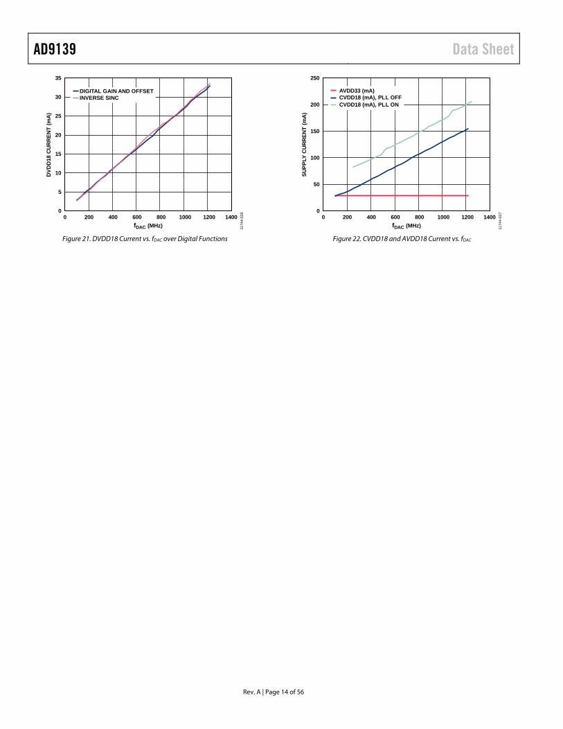
AD9139 Data Sheet
Figure 21. DVDD18 Current vs. fDAC over Digital Functions
Figure 22. CVDD18 and AVDD18 Current vs. fDAC
35
30
25
20
15
10
5
DVD
D18
CU
RR
ENT
(mA
)
00 200 400
DIGITAL GAIN AND OFFSETINVERSE SINC
600 800 1000 1200 1400fDAC (MHz) 11
744-
026
250
200
150
100
50
SUPP
LY C
UR
REN
T (m
A)
00 200 400 600 800 1000 1200 1400
fDAC (MHz) 1174
4-02
7
AVDD33 (mA)CVDD18 (mA), PLL OFFCVDD18 (mA), PLL ON
Rev. A | Page 14 of 56

Data Sheet AD9139
TERMINOLOGY Integral Nonlinearity (INL) INL is the maximum deviation of the actual analog output from the ideal output, determined by a straight line drawn from zero scale to full scale.
Differential Nonlinearity (DNL) DNL is the measure of the variation in analog value, normalized to full scale, associated with a 1 LSB change in digital input code.
Offset Error Offset error is the deviation of the output current from the ideal of 0 mA. For DACOUTP, 0 mA output is expected when all inputs are set to 0. For DACOUTN, 0 mA output is expected when all inputs are set to 1.
Gain Error Gain error is the difference between the actual and ideal output span. The actual span is determined by the difference between the output when all inputs are set to 1 and the output when all inputs are set to 0.
Output Compliance Range The output compliance range is the range of allowable voltage at the output of a current output DAC. Operation beyond the maximum compliance limits can cause either output stage saturation or breakdown, resulting in nonlinear performance.
Temperature Drift Temperature drift is specified as the maximum change from the ambient (25°C) value to the value at either TMIN or TMAX. For offset and gain drift, the drift is reported in ppm of full-scale range (FSR) per degree Celsius. For reference drift, the drift is reported in ppm per degree Celsius.
Power Supply Rejection (PSR) PSR is the maximum change in the full-scale output as the supplies are varied from minimum to maximum specified voltages.
Settling Time Settling time is the time required for the output to reach and remain within a specified error band around its final value, measured from the start of the output transition.
Spurious Free Dynamic Range (SFDR) SFDR is the difference, in decibels, between the peak amplitude of the output signal and the peak spurious signal within the dc to Nyquist frequency of the DAC. Typically, the interpolation filters reject energy in this band. This specification, therefore, defines how well the interpolation filters work and the effect of other parasitic coupling paths on the DAC output.
Signal-to-Noise Ratio (SNR) SNR is the ratio of the rms value of the measured output signal to the rms sum of all other spectral components below the Nyquist frequency, excluding the first six harmonics and dc. The value for SNR is expressed in decibels.
Interpolation Filter If the digital inputs to the DAC are sampled at a multiple rate of fDATA (interpolation rate), a digital filter can be constructed that has a sharp transition band near fDATA/2. Images that typically appear around fDAC (output data rate) can be greatly suppressed.
Adjacent Channel Leakage Ratio (ACLR) ACLR is the ratio in decibels relative to the carrier (dBc) between the measured power within a channel relative to its adjacent channel.
Complex Image Rejection In a traditional two-part upconversion, two images are created around the second IF frequency. These images have the effect of wasting transmitter power and system bandwidth. By placing the real part of a second complex modulator in series with the first complex modulator, either the upper or lower frequency image near the second IF can be rejected.
Rev. A | Page 15 of 56

AD9139 Data Sheet
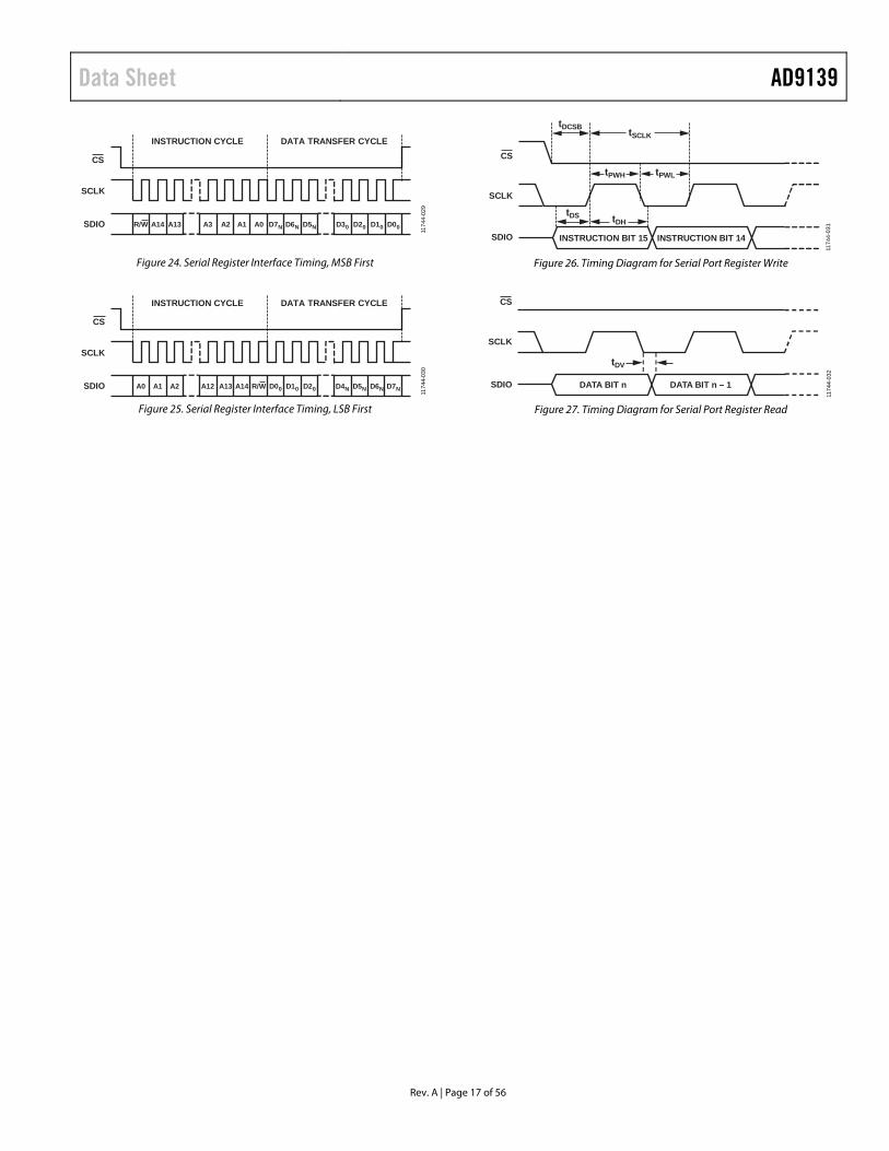
SERIAL PORT OPERATION The serial port is a flexible, synchronous serial communications port that allows easy interfacing to many industry standard micro-controllers and microprocessors. The serial I/O is compatible with most synchronous transfer formats, including both the Motorola SPI and Intel® SSR protocols. The interface allows read/write access to all registers that configure the AD9139. MSB first or LSB first transfer formats are supported. The serial port interface is a 3-wire only interface. The input and output share a single input/output (SDIO) pin.
Figure 23. Serial Port Interface Pins
There are two phases to a communication cycle with the AD9139. Phase 1 is the instruction cycle (the writing of an instruction byte into the device), coincident with the first 16 SCLK rising edges. The instruction word provides the serial port controller with information regarding the data transfer cycle, Phase 2, of the communication cycle. The Phase 1 instruction word defines whether the upcoming data transfer is a read or write, together with the starting register address for the following data transfer.
A logic high on the CS pin, followed by a logic low, resets the serial port timing to the initial state of the instruction cycle. From this state, the next 16 rising SCLK edges represent the instruction bits of the current I/O operation.
The remaining SCLK edges are for Phase 2 of the communication cycle. Phase 2 is the actual data transfer between the device and the system controller. Phase 2 of the communication cycle is a transfer of one data byte. Registers change immediately upon writing to the last bit of each transfer byte.
DATA FORMAT The instruction byte contains the information shown in Table 9.
Table 9. Serial Port Instruction Word I15 (MSB) I[14:0] R/W A[14:0]
R/W (Bit 15 of the instruction word) determines whether a read or a write data transfer occurs after the instruction word write. Logic 1 indicates a read operation, and Logic 0 indicates a write operation.
A14 to A0 (Bit 14 to Bit 0 of the instruction word) determine the register that is accessed during the data transfer portion of the communication cycle. For multibyte transfers, A14 is the starting address; the device generates the remaining register addresses based on the SPI_LSB_FIRST bit.
SERIAL PORT PIN DESCRIPTIONS Serial Clock (SCLK)
The serial clock pin, SCLK, synchronizes data to and from the device and runs the internal state machines. The maximum frequency of SCLK is 40 MHz. All data input is read on the rising edge of SCLK. All data is driven out on the falling edge of SCLK.
Chip Select (CS)
CS is an active low input that starts and gates a communication cycle. It allows the use of multiple devices on the same serial communications line. The SDIO pin enters a high impedance state when the CS input is high. During the communication cycle, CS remains low.
Serial Data I/O (SDIO)
The SDIO pin is a bidirectional data line.
SERIAL PORT OPTIONS The serial port supports both MSB first and LSB first data formats; the SPI_LSB_FIRST bit (Register 0x00, Bit 6) controls this functionality. The default is MSB first (SPI_LSB_FIRST = 0).
When SPI_LSB_FIRST = 0 (MSB first), the instruction and data bits must be written from MSB to LSB. Multibyte data transfers in MSB first format start with an instruction word that includes the register address of the most significant data byte. Subsequent data bytes must follow from high address to low address. In MSB first mode, the serial port internal word address generator decrements for each data byte of the multibyte communication cycle.
When SPI_LSB_FIRST = 1 (LSB first), the instruction and data bits must be written from LSB to MSB. Multibyte data transfers in LSB first format start with an instruction word that includes the register address of the least significant data byte. Subsequent data bytes must follow from low address to high address. In LSB first mode, the serial port internal word address generator increments for each data byte of the multibyte communication cycle.
When the MSB first mode is active, the serial port controller data address decrements from the data address written toward 0x00 for multibyte I/O operations. If the LSB first mode is active, the serial port controller data address increments from the data address written toward 0xFF for multibyte I/O operations.
53 SCLK
54 CS
52 SDIO
SPIPORT
1174
4-02
8
Rev. A | Page 16 of 56
Data Sheet AD9139
Figure 24. Serial Register Interface Timing, MSB First
Figure 25. Serial Register Interface Timing, LSB First
Figure 26. Timing Diagram for Serial Port Register Write
Figure 27. Timing Diagram for Serial Port Register Read
R/W A14 A13 A3 A2 A1 A0 D7N D6N D5N D00D10D20D30
INSTRUCTION CYCLE DATA TRANSFER CYCLE
SCLK
SDIO
CS
1174
4-02
9
A0 A1 A2 A12 A13 A14 R/W D00 D10 D20 D7ND6ND5ND4N
INSTRUCTION CYCLE DATA TRANSFER CYCLE
SCLK
SDIO
CS
1174
4-03
0
SCLK
SDIO
CS
INSTRUCTION BIT 14INSTRUCTION BIT 15
tDCSB
tDS tDH
tPWH tPWL
tSCLK
1174
4-03
1
SCLK
SDIO
CS
DATA BIT n – 1DATA BIT n
tDV
1174
4-03
2
Rev. A | Page 17 of 56
AD9139 Data Sheet
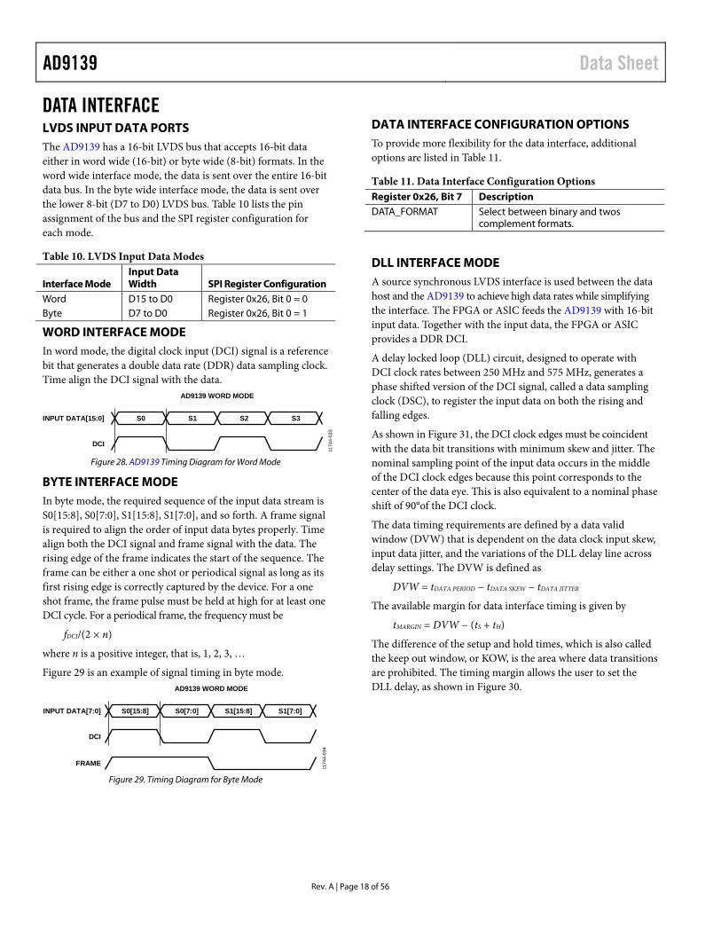
DATA INTERFACE LVDS INPUT DATA PORTS The AD9139 has a 16-bit LVDS bus that accepts 16-bit data either in word wide (16-bit) or byte wide (8-bit) formats. In the word wide interface mode, the data is sent over the entire 16-bit data bus. In the byte wide interface mode, the data is sent over the lower 8-bit (D7 to D0) LVDS bus. Table 10 lists the pin assignment of the bus and the SPI register configuration for each mode.
Table 10. LVDS Input Data Modes
Interface Mode Input Data Width SPI Register Configuration
Word D15 to D0 Register 0x26, Bit 0 = 0 Byte D7 to D0 Register 0x26, Bit 0 = 1
WORD INTERFACE MODE In word mode, the digital clock input (DCI) signal is a reference bit that generates a double data rate (DDR) data sampling clock. Time align the DCI signal with the data.
Figure 28. AD9139 Timing Diagram for Word Mode
BYTE INTERFACE MODE In byte mode, the required sequence of the input data stream is S0[15:8], S0[7:0], S1[15:8], S1[7:0], and so forth. A frame signal is required to align the order of input data bytes properly. Time align both the DCI signal and frame signal with the data. The rising edge of the frame indicates the start of the sequence. The frame can be either a one shot or periodical signal as long as its first rising edge is correctly captured by the device. For a one shot frame, the frame pulse must be held at high for at least one DCI cycle. For a periodical frame, the frequency must be
fDCI/(2 × n)
where n is a positive integer, that is, 1, 2, 3, …
Figure 29 is an example of signal timing in byte mode.
Figure 29. Timing Diagram for Byte Mode
DATA INTERFACE CONFIGURATION OPTIONS To provide more flexibility for the data interface, additional options are listed in Table 11.
Table 11. Data Interface Configuration Options Register 0x26, Bit 7 Description DATA_FORMAT Select between binary and twos
complement formats.
DLL INTERFACE MODE A source synchronous LVDS interface is used between the data host and the AD9139 to achieve high data rates while simplifying the interface. The FPGA or ASIC feeds the AD9139 with 16-bit input data. Together with the input data, the FPGA or ASIC provides a DDR DCI.
A delay locked loop (DLL) circuit, designed to operate with DCI clock rates between 250 MHz and 575 MHz, generates a phase shifted version of the DCI signal, called a data sampling clock (DSC), to register the input data on both the rising and falling edges.
As shown in Figure 31, the DCI clock edges must be coincident with the data bit transitions with minimum skew and jitter. The nominal sampling point of the input data occurs in the middle of the DCI clock edges because this point corresponds to the center of the data eye. This is also equivalent to a nominal phase shift of 90°of the DCI clock.
The data timing requirements are defined by a data valid window (DVW) that is dependent on the data clock input skew, input data jitter, and the variations of the DLL delay line across delay settings. The DVW is defined as
DVW = tDATA PERIOD − tDATA SKEW − tDATA JITTER
The available margin for data interface timing is given by
tMARGIN = DVW − (tS + tH)
The difference of the setup and hold times, which is also called the keep out window, or KOW, is the area where data transitions are prohibited. The timing margin allows the user to set the DLL delay, as shown in Figure 30.
S0 S1 S2 S3
AD9139 WORD MODE
DCI
INPUT DATA[15:0]
1174
4-03
3
S0[15:8] S0[7:0] S1[15:8] S1[7:0]
AD9139 WORD MODE
DCI
FRAME
INPUT DATA[7:0]
1174
4-03
4
Rev. A | Page 18 of 56

Data Sheet AD9139
Figure 30. LVDS Data Port Timing Requirements
Figure 30 shows that the ideal location for the DSC signal is 90° out of phase from the DCI input; however, due to skew of the DCI relative to the data, it may be necessary to change the DSC phase offset to sample the data at the center of its eye diagram. Vary the sampling instance in discrete increments by offsetting the nominal DLL phase shift value of 90° via Register 0x0A, Bits[3:0]. This register is a signed value. The MSB is the sign and the LSBs are the magnitude. The following equation defines the phase offset relationship:
Phase Offset = 90° + n × 11.25°, |n| < 7
where n is the DLL phase offset setting.
Figure 31 shows the DSC setup and hold times with respect to the DCI signal and data signals.
Figure 31. LVDS Data Port Setup and Hold Times
Table 12 lists the guaranteed values across the operating condi-tions. These values were obtained using a 50% duty cycle and a DCI swing of 450 mV p-p. For best performance, maintain a duty cycle variation below ±5% and set the DCI input as high as possible, up to 1200 mV p-p.
Table 12. DLL Phase Setup and Hold Times (Guaranteed)
Frequency, fDCI (MHz) Time (ps)
Data Port Setup and Hold Times (ps) at DLL Phase
−3 0 +3 307 tS −125 −385 −695
tH 834 1120 1417
368 tS −70 −305 −534
tH 753 967 1207
491 tS −81 −245 −402
tH 601 762 928
614 tS −54.0 −167 −277
tH 497 603 721
DATA EYEINPUT DATA
DCI
DATA SAMPLE CLOCK
INPUT DATA
DCI
DLLPHASEDELAY
tDATA JITTER
tDATA JITTER
DATA SAMPLE CLOCK
tH
tS
tH + tS
tDCI SKEW
tDATA PERIOD
DATA EYE
tDATA PERIOD
1174
4-03
5
1174
4-03
6
DCI
DATA
DSC
tS
tH
Rev. A | Page 19 of 56

AD9139 Data Sheet
Table 13. DLL Phase Setup and Hold Times (Typical) Frequency, fDCI1 (MHz)
Time (ps)
Data Port Setup and Hold Times (ps) at DLL Phase
−6 −5 −4 −3 −2 −1 0 +1 +2 +3 +4 +5 +6 250 tS −93 −196 −312 −416 −530 −658 −770 −878 −983 −1093 −1193 −1289 −1412
tH 468 579 707 825 947 1067 1188 1315 1442 1570 1697 1777 1876 275 tS −87 −172 −264 −364 −464 −556 −653 −756 −859 −956 −1053 −1151 −1251
tH 451 537 646 757 878 977 1092 1218 1311 1423 1537 1653 1728 300 tS −82 −166 −256 −341 −426 −515 −622 −715 −809 −900 −1001 −1097 −1184
tH 422 500 598 703 803 897 1000 1105 1203 1303 1411 1522 1612 325 tS −46 −114 −190 −271 −358 −447 −538 −612 −706 −806 −891 −966 −1044
tH 405 483 563 647 740 832 914 1000 1100 1200 1292 1380 1476 350 tS −23 −92 −180 −252 −328 −409 −491 −574 −654 −731 −819 −889 −959
tH 383 451 524 607 682 762 844 930 1011 1097 1186 1277 1358 375 tS −7 −82 −150 −225 −315 −391 −461 −526 −595 −661 −726 −786 −853
tH 401 466 504 569 641 718 783 863 941 1025 1106 1187 1264 400 tS −46 −98 −161 −243 −303 −384 −448 −513 −578 −643 −713 −771 −833
tH 385 445 503 546 604 674 748 826 890 965 1039 1110 1178 425 tS 4 −52 −110 −170 −229 −297 −394 −449 −517 −579 −641 −704 −752
tH 358 408 465 524 595 625 692 762 829 900 966 1032 1097 450 tS 11 −34 −92 −147 −209 −269 −324 −386 −446 −509 −564 −622 −672
tH 354 406 457 516 573 637 693 731 792 852 917 983 1042 475 tS −15 −51 −95 −147 −198 −255 −313 −366 −425 −480 −530 −585 −640
tH 355 399 451 499 556 613 675 727 779 815 873 930 988 500 tS 9 −28 −77 −128 −183 −233 −288 −333 −390 −438 −495 −545 −594
tH 313 354 399 445 500 555 615 668 726 783 825 881 934 525 tS −7 −52 −100 −147 −187 −237 −285 −335 −387 −436 −483 −530 −581
tH 311 356 395 438 489 537 592 645 692 746 799 850 909 550 tS −5 −39 −74 −107 −147 −192 −249 −302 −352 −397 −440 −486 −529
tH 300 340 378 423 468 510 560 610 659 710 756 810 865 575 tS 8 −28 −66 −102 −143 −181 −245 −280 −336 −366 −406 −443 −488
tH 312 348 379 414 453 496 544 599 654 708 759 806 847
1 Table 13 shows characterization data for selected fDCI frequencies. Other frequencies are possible; use Table 13 to estimate performance.
Table 13 shows the typical times for various DCI clock frequencies that are required to calculate the data valid margin. Use Table 13 to determine the amount of margin that is available for tuning of the DSC sampling point.
Maximizing the opening of the eye in both the DCI and data signals improves the reliability of the data port interface. Use differential controlled impedance traces of equal length (that is, delay) between the host processor and the AD9139 input. To ensure coincident transitions with the data bits, implement the DCI signal as an additional data line with an alternating (010101…) bit sequence from the same output drivers that are used for the data.
The DCI signal is ac-coupled by default; thus, removing the DCI signal may cause DAC output chatter due to randomness on the DCI input. To avoid this, disable the DAC output whenever the DCI signal is not present by setting the DAC output current power-down bit in Register 0x01[7] to 1. When the DCI signal is again present, enable the DAC output by programming Register 0x01[7] to 0.
Register 0x0D optimizes the DLL stability over the operating frequency range. Table 14 shows the recommended settings.
Table 14. DLL Configuration Options DCI Speed Register 0x0D ≥350 MHz 0x06 <350 MHz 0x86
Poll the status of the DLL by reading the data status register at Address 0x0E. Bit 0 indicates that the DLL is running and attempting lock; Bit 7 is 1 when the DLL has locked. Bit 2 is 1 when a valid data clock input (DCI) is detected. The warning bits in [6:4] in Register 0x0E can be used as indicators that the DAC may be operating in a nonideal location in the delay line. Note that these bits are read at the SPI port speed, which is much slower than the actual speed of the DLL. This means they can only show a snapshot of what is happening as opposed to giving real-time feedback.
Rev. A | Page 20 of 56

Data Sheet AD9139 DLL Configuration Example 1
In the following DLL configuration example, fDCI = 600 MHz, DLL is enabled, and DLL phase offset = 0.
1. 0x5E → 0xFE /* Turn off LSB delay cell*/ 2. 0x0D → 0x06 /* Select DLL configure
options */
3. 0x0A → 0xC0 /* Enable DLL and duty cycle correction. Set DLL phase offset to 0 */
4. Read 0x0E[7:4] /* Expect 1000b if the DLL is locked */
DLL Configuration Example 2
In the following DLL configuration example, fDCI = 300 MHz, DLL is enable, and DLL phase offset = 0.
1. 0x5E → 0xFE /* Turn off LSB delay cell*/ 2. 0x0D → 0x86 /* Select DLL configure
options */
3. 0x0A → 0xC0 /* Enable DLL and duty cycle correction. Set DLL phase offset to 0 */
4. Read 0x0E[7:4] /* Expect 1000b if the DLL is locked */
PARITY The data interface can be continuously monitored by enabling the parity bit feature in Register 0x6A[7] and configuring the frame/parity bit as parity by setting Register 0x09 = 0x21. In this case, the host sends a parity bit with each data sample. This bit is set according to the following formulas, where n is the data sample that is being checked:
For even parity,
XOR[FRM(n), D0(n), D1(n), D2(n), …, D15(n)] = 0
For odd parity,
XOR[FRM(n), D0(n), D1(n), D2(n), …, D15(n)] = 1
The parity bit is calculated over 17 bits (including the frame/parity bit).
If a parity error occurs, the parity error counter (Register 0x6B or Register 0x6C) increments. Parity errors on the bits sampled by the rising edge of the DCI signal increment the rising edge parity counter (Register 0x6B) and set the PARERRRIS bit (Register 0x6A[0]). Parity errors on the bits sampled by the falling edge of DCI increment the falling edge parity counter (Register 0x6C) and set the PARERRFAL bit (Register 0x6A[1]). The parity counter continues to accumulate until it clears or until it reaches a maximum value of 255. To clear the count, write a 1 to Register 0x6A[5].
To trigger an IRQ when a parity error occurs, write 1 to Bit 7 in Register 0x04. This IRQ triggers when there is either a rising edge or falling edge parity error. Observe the status of the IRQ pin via Register 0x06[7] or by using the selected IRQx pin. Clear the IRQ by writing a 1 to Register 0x06[7].
Use the parity bit feature to validate the interface timing. As described previously, the host provides a parity bit with the data
samples, as well as configures the AD9139 to generate an IRQ. The user can then sweep the sampling instance of the input registers of the AD9139 to determine at what point sampling errors occur. The sampling instance can be varied in discrete increments by offsetting the nominal DLL phase shift value of 90° via SPI Register 0x0A[3:0].
SED OPERATION The AD9139 provides on-chip sample error detection (SED) circuitry that simplifies verification of the input data interface. The SED compares the input data samples captured at the digital input pins with a set of comparison values. The comparison values are loaded into registers through the SPI port. Differences between the captured values and the comparison values are detected. Options are available for customizing SED test sequencing and error handling.
The SED circuitry allows the application to test a short user defined pattern to confirm that the high speed source synchronous data bus is correctly implemented and meets the timing requirement. Unlike the parity bit, the SED circuitry is expected to be used during initial system calibration, before the AD9139 is in use in the application. The SED circuitry operates on a data set made up of user defined input words, denoted as S0, S1, S2, and S3. The user defined pattern consists of sequential data-word samples (S0 is sampled on the rising edge of DCI, S1 is sampled on the following falling edge of DCI, S2 is sampled on the following DCI rising edge, and S3 is sampled on the following DCI falling edge). The user loads this data pattern in the byte format into Register 0x61 through Register 0x68.
The depth of the user defined pattern is selectable via Bit 4 of the SED_CTRL register (0x60). A default of 0, means a depth of two (using S0 and S1), and a 1 means a depth of four (using S0, S1, S2, and S3, and requiring the use of frame signal input to define S0 to the SED state machine). To properly align the input samples using a depth of 4, S0 is indicated by asserting the frame signal for a minimum of two complete input samples as shown in. The frame signal can be issued once at the start of the data transmission, or it can be asserted repeatedly at intervals coinciding with the S0 word.
Figure 32. Timing Diagram of Extended FRAMEx Signal Required to Align
Input Data for SED
The SED has three flag bits (Register 0x60, Bit 0, Bit 1, and Bit 2) that indicate the results of the input sample comparisons. The sample error detected bit (Register 0x60, Bit 0) is set when an error is detected and remains set until cleared.
The autosample error detection (AED) mode is an autoclear mode that has two effects: it activates the compare fail bit and the compare pass bit (Register 0x60, Bit 1 and Bit 2). The compare pass bit sets if the last comparison indicated the sample was error free. The compare fail bit sets if an error is
FRAME
S3S1S0 S2 S0 S1DATA[15:0]
1174
4-03
7
Rev. A | Page 21 of 56

AD9139 Data Sheet detected. The compare fail bit is automatically cleared by the reception of eight consecutive error free comparisons when autoclear mode is enabled.
The sample error flag can be configured to trigger an IRQ when active, if desired, by enabling the appropriate bit in the event flag register (Register 0x04, Bit 6).
SED EXAMPLE Normal Operation
The following example illustrates the AD9139 SED configuration for continuously monitoring the input data and assertion of an IRQ when a single error is detected.
1. Write to the following registers to enable the SED and load the comparison values with a four-deep user pattern. Comparison values can be chosen arbitrarily; however, choosing values that require frequent bit toggling provides the most robust test. a. Register 0x61[7:0]→ S0[7:0] b. Register 0x62[7:0]→ S0[15:8] c. Register 0x63[7:0]→ S1[7:0] d. Register 0x64[7:0]→ S1[15:8] e. Register 0x65[7:0]→ S2[7:0] f. Register 0x66[7:0]→ S2[15:8] g. Register 0x67[7:0]→ S3[7:0] h. Register 0x68[7:0]→ S3[15:8]
2. Enable SED. a. Register 0x60 → 0xD0 b. Register 0x60 → 0x90
3. Enable the SED error detect flag to assert the IRQx pin. a. Register 0x04[6] = 1
4. Begin transmitting the input data pattern (FRAMEx is also required because the depth of the pattern is 4).
DELAY LINE INTERFACE MODE The DLL is designed to help ease the interface timing require-ments in very high speed data rate applications. The DLL has a minimum supported interface speed of 250 MHz, as shown in Table 2. For interface rates below this speed, use the interface delay line. In this mode, the DLL is powered off and a four-tap delay line is provided for the user to adjust the timing between the data bus and the DCI. Table 15 specifies the setup and hold times for each delay tap.
Table 15. Delay Line Setup and Hold Times (Guaranteed) Delay Setting 0 1 2 3 Register 0x5E[7:0] 0x00 0x80 0xF0 0xFE Register 0x5F[2:0] 0x60 0x67 0x67 0x67 tS (ns)1 −0.81 −0.97 −1.13 −1.28 tH (ns) 1.96 2.20 2.53 2.79 |tS + tH| (ns) 1.15 1.23 1.40 1.51 1 The negative sign indicates the direction of the setup time. The setup time is
defined as positive when it is on the left side of the clock edge and negative when it is on the right side of the clock edge.
There is a fixed 1.38 ns delay on the DCI signal when the delay line is enabled. Each tap adds a nominal delay of 200 ps to the fixed delay. To achieve the best timing margin, that is, to center the setup and hold window in the middle of the data eye, the user may need to add a delay on the data bus with respect to the DCI signal in the data source. Figure 33 is an example of calculating the optimal external delay.
Register 0x0D[4] configures the DCI signal coupling settings for optimal interface performance over the operating frequency range. It is recommended that this bit be set to 1 (dc-coupled DCI) in the delay line interface mode.
Figure 33. Example of Interfacing Timing in the Delay Line-Based Mode
DCI = 200MHz
|tS| = 0.81ns
|tH| = 1.96ns
tDELAY = 0.13nstDATA PERIOD = 2.5ns
DATA EYEINPUT DATA[15:0]
WITHOPTIMIZED DELAY
NO DATA TRANSITION
1174
4-03
8
Rev. A | Page 22 of 56

Data Sheet AD9139 Interface Timing Requirements
The following example shows how to calculate the optimal delay at the data source to achieve the best sampling timing in the delay line interface mode:
• fDCI = 200 MHz • Delay setting = 0
The shadow area in Figure 33 is the interface setup and hold time window set to 0. To optimize the interface timing, this window must be placed in the middle of the data transitions. Because the input is double data rate, the available data period is 2.5 ns. Therefore, the optimal data bus delay, with respect to the DCI signal at the data source, can be calculated as
ns13.025.138.122
|)||(|=−=−
+= PERIODDATAHS
DELAY
tttt
SPI Sequence to Enable Delay Line-Based Mode
Use the following SPI sequence to enable the delay line-based mode:
1. 0x5E → 0x00 /* Configure the delay setting */
2. 0x5F → 0x60
3. 0x0D → 0x16 /* DC couple DCI */
4. 0x0A → 0x00 /* Turn off DLL and duty cycle correction */
Rev. A | Page 23 of 56

AD9139 Data Sheet
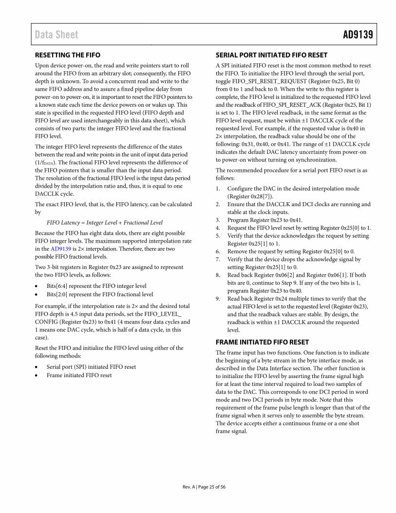
FIFO OPERATION The AD9139 adopts source synchronous clocking in the data receiver (see the Data Interface section). The nature of source synchronous clocking is the creation of a separate clock domain at the receiving device. In the DAC, it is the DAC clock domain, that is, the DACCLK. Therefore, there are two clock domains inside of the DAC: the DCI and the DACCLK. Often, these two clock domains are not synchronous, requiring an additional stage to adjust the timing for proper data transfer. In the AD9139, a FIFO stage is inserted between the DCI and DACCLK domains to transfer the received data into the core clock domain (DACCLK) of the DAC.
The AD9139 contains a 2-channel, 16-bit wide, eight-word deep FIFO. The FIFO acts as a buffer that absorbs timing variations between the two clock domains. The timing budget between the two clock domains in the system is significantly relaxed due to the depth of the FIFO.
Figure 34 shows the block diagram of the datapath through the FIFO. The input data is latched into the device, formatted, and then written into the FIFO register, which is determined by the FIFO write pointer. The value of the write pointer is incremented
every time a new word is loaded into the FIFO. Meanwhile, data is read from the FIFO register, which is determined by the read pointer, and fed into the digital datapath. The value of the read pointer is incremented every time data is read into the datapath from the FIFO. The FIFO pointers are incremented at the data rate, which is the DACCLK rate divided by the interpolation rate.
Valid data is transmitted through the FIFO as long as the FIFO does not overflow (full) or underflow (empty). An overflow or underflow condition occurs when the write pointer and read pointer point to the same FIFO slot. This simultaneous access of data leads to unreliable data transfer through the FIFO and must be avoided.
Normally, data is written to and read from the FIFO at the same rate to maintain a constant FIFO depth. If data is written to the FIFO faster than data is read, the FIFO depth increases. If data is read from the FIFO faster than data is written to it, the FIFO depth decreases. For optimal timing margin, maintain the FIFO depth near half full (a difference of four between the write pointer and read pointer values). The FIFO depth represents the FIFO pipeline delay and is part of the overall latency of the AD9139.
Figure 34. Block Diagram of FIFO
DATARECEIVER
DATAFORMAT
RESETLOGIC
DATA PATH DAC
FIFO SLOT 0
FIFO SLOT 1
FIFO SLOT 2
FIFO SLOT 3
FIFO SLOT 4
FIFO SLOT 5
FIFO SLOT 6
FIFO SLOT 7
INPUT DATA[15:0]
DCI
FRAME
[15:0]LATCHED
DATA[15:0]
RETIMED DCI
SPI FIFO RESETREG 0x25[0]
[15:0] [15:0]
÷INTDACCLK
FIFO LEVEL REQUESTREG 0x23
FIFO WRITE CLOCK FIFO READ CLOCK
WRITEPOINTER
READ POINTER
FIFO
FIFO LEVEL11
744-
039
Rev. A | Page 24 of 56
Data Sheet AD9139
RESETTING THE FIFO Upon device power-on, the read and write pointers start to roll around the FIFO from an arbitrary slot; consequently, the FIFO depth is unknown. To avoid a concurrent read and write to the same FIFO address and to assure a fixed pipeline delay from power-on to power-on, it is important to reset the FIFO pointers to a known state each time the device powers on or wakes up. This state is specified in the requested FIFO level (FIFO depth and FIFO level are used interchangeably in this data sheet), which consists of two parts: the integer FIFO level and the fractional FIFO level.
The integer FIFO level represents the difference of the states between the read and write points in the unit of input data period (1/fDATA). The fractional FIFO level represents the difference of the FIFO pointers that is smaller than the input data period. The resolution of the fractional FIFO level is the input data period divided by the interpolation ratio and, thus, it is equal to one DACCLK cycle.
The exact FIFO level, that is, the FIFO latency, can be calculated by
FIFO Latency = Integer Level + Fractional Level
Because the FIFO has eight data slots, there are eight possible FIFO integer levels. The maximum supported interpolation rate in the AD9139 is 2× interpolation. Therefore, there are two possible FIFO fractional levels.
Two 3-bit registers in Register 0x23 are assigned to represent the two FIFO levels, as follows:
• Bits[6:4] represent the FIFO integer level • Bits[2:0] represent the FIFO fractional level
For example, if the interpolation rate is 2× and the desired total FIFO depth is 4.5 input data periods, set the FIFO_LEVEL_ CONFIG (Register 0x23) to 0x41 (4 means four data cycles and 1 means one DAC cycle, which is half of a data cycle, in this case).
Reset the FIFO and initialize the FIFO level using either of the following methods:
• Serial port (SPI) initiated FIFO reset • Frame initiated FIFO reset
SERIAL PORT INITIATED FIFO RESET A SPI initiated FIFO reset is the most common method to reset the FIFO. To initialize the FIFO level through the serial port, toggle FIFO_SPI_RESET_REQUEST (Register 0x25, Bit 0) from 0 to 1 and back to 0. When the write to this register is complete, the FIFO level is initialized to the requested FIFO level and the readback of FIFO_SPI_RESET_ACK (Register 0x25, Bit 1) is set to 1. The FIFO level readback, in the same format as the FIFO level request, must be within ±1 DACCLK cycle of the requested level. For example, if the requested value is 0x40 in 2× interpolation, the readback value should be one of the following: 0x31, 0x40, or 0x41. The range of ±1 DACCLK cycle indicates the default DAC latency uncertainty from power-on to power-on without turning on synchronization.
The recommended procedure for a serial port FIFO reset is as follows:
1. Configure the DAC in the desired interpolation mode (Register 0x28[7]).
2. Ensure that the DACCLK and DCI clocks are running and stable at the clock inputs.
3. Program Register 0x23 to 0x41. 4. Request the FIFO level reset by setting Register 0x25[0] to 1. 5. Verify that the device acknowledges the request by setting
Register 0x25[1] to 1. 6. Remove the request by setting Register 0x25[0] to 0. 7. Verify that the device drops the acknowledge signal by
setting Register 0x25[1] to 0. 8. Read back Register 0x06[2] and Register 0x06[1]. If both
bits are 0, continue to Step 9. If any of the two bits is 1, program Register 0x23 to 0x40.
9. Read back Register 0x24 multiple times to verify that the actual FIFO level is set to the requested level (Register 0x23), and that the readback values are stable. By design, the readback is within ±1 DACCLK around the requested level.
FRAME INITIATED FIFO RESET The frame input has two functions. One function is to indicate the beginning of a byte stream in the byte interface mode, as described in the Data Interface section. The other function is to initialize the FIFO level by asserting the frame signal high for at least the time interval required to load two samples of data to the DAC. This corresponds to one DCI period in word mode and two DCI periods in byte mode. Note that this requirement of the frame pulse length is longer than that of the frame signal when it serves only to assemble the byte stream. The device accepts either a continuous frame or a one shot frame signal.
Rev. A | Page 25 of 56
AD9139 Data Sheet In the continuous reset mode, the FIFO responds to every valid frame pulse and resets itself. In the one shot reset mode, the FIFO responds only to the first valid frame pulse after the FRAME_RESET_MODE bits (Register 0x22[1:0]) are set. Therefore, even with a continuous frame input, the FIFO resets one time only; this prevents the FIFO from toggling between the two states from periodic resets. The one shot frame reset mode is the default and the recommended mode.
The recommended procedure for a frame initiated FIFO reset is as follows:
1. Configure the DAC in the desired interpolation mode (Register 0x28[7]).
2. Ensure that the DACCLK and DCI clocks are running and stable at the clock inputs.
3. Ensure that the DLL is locked (if using DLL Mode) or the DCI clock is being sent properly (if using bypass mode).
4. Program Register 0x23 to 0x41. 5. Configure the FRAME_RESET_MODE bits
(Register 0x22[1:0]) to 10. 6. Choose one shot frame mode by writing 0 to
EN_CON_FRAME_RESET (Register 0x22[2]). 7. Toggle the frame input from 0 to 1 and back to 0. The pulse
width must be longer than the minimum requirement. 8. Read back Register 0x06[2] and Register 0x06[1]. If both
bits are 0, continue to Step 9. If any of the two bits are 1, program Register 0x23 to 0x40.
9. Read back Register 0x24 multiple times to verify that the actual FIFO level is set to the requested level (Register 0x23) and the readback values are stable. By design, the readback should be within ±1 DACCLK around the requested level.
These procedures apply in synchronization off mode only. For resetting FIFO in synchronization on mode, refer to the synchronization procedure in the Multidevice Synchronization and Fixed Latency section. FIFO reset is one of the steps to achieve synchronization.
Monitoring the FIFO Status
Monitor the real-time FIFO status from SPI Register 0x24, which reflects the real-time FIFO depth after a FIFO reset. Without timing drifts in the system, this readback does not change from that which resulted from the FIFO reset. When there is a timing drift or other abnormal clocking situation, the FIFO level readback can change. However, as long as the FIFO does not overflow or underflow, there is no error in data trans-mission. The status bits in Register 0x06, Bits[2:1] indicate if there are FIFO underflows or overflows. Latch the status of the two bits to trigger the hardware interrupts, IRQ1 and IRQ2. To enable latching and interrupts, configure the corresponding bits in Register 0x03 and Register 0x04.
Rev. A | Page 26 of 56

Data Sheet AD9139
Rev. A | Page 27 of 56
DIGITAL DATAPATH The block diagram in Figure 35 shows the functionality of the digital datapath. The digital processing includes
One half-band interpolation filter An inverse sinc filter A gain and offset adjustment block
Figure 35. Block Diagram of Digital Datapath
INTERPOLATION FILTERS The transmit path contains a half-band interpolation filter. The interpolation filters provides a 2× increase in output data rate and a low-pass function.
The AD9139 provides two interpolation modes. Each mode offers a different usable signal bandwidth in an operating mode. Which mode to select depends on the required signal bandwidth and the DAC update rate. Refer to Table 5 for the maximum speed and signal bandwidth of each interpolation mode.
The usable bandwidth in 1× interpolation is the DCI rate or half of the input data rate. The usable bandwidth in 2× interpolation is 0.8 times the DCI rate or 0.4 times the input data rate. It is defined as the frequency band over which the filters have a pass-band ripple of less than ±0.001 dB and a stop-band rejection of greater than 85 dB.
2× Interpolation Mode
Figure 36 and Figure 37 show the pass-band and all-band filter response for 2× mode. Note that the transition from the transition band to the stop band is much sharper than the tran-sition from the pass band to the transition band. Therefore, when the desired output signal moves out of the defined pass band, the signal image, which is supposed to be suppressed by the stop band, grows faster than the droop of the signal itself due to the degraded pass-band flatness. In cases where the degraded image rejection is acceptable or can be compensated by the analog low-pass filter at the DAC output, it is possible to let the output signal extend beyond the specified usable signal bandwidth.
Figure 36. Pass-Band Detail of 2× Mode
Figure 37. All-Band Response of 2× Mode
HB1 INVSINC
DIGITAL GAINAND OFFSETADJUSTMENT
1174
4-04
0
0.02
–0.10
–0.08
–0.06
–0.04
–0.02
0
0 0.05 0.10 0.15 0.20 0.25 0.30 0.35 0.40 0.45
MA
GN
ITU
DE
(dB
)
FREQUENCY (Hz) 1174
4-04
1
10
–100
–90
–80
–70
–60
–50
–40
–30
–20
–10
0
0 0.40.2 0.6 0.8 1.0 1.2 1.4 1.6 1.8 2.0
MA
GN
ITU
DE
(dB
)
FREQUENCY (Hz) 1174
4-04
2

AD9139 Data Sheet
Table 16. Half-Band Filter 1 Coefficient Lower Coefficient Upper Coefficient Integer Value H(1) H(55) −4 H(2) H(54) 0 H(3) H(53) +13 H(4) H(52) 0 H(5) H(51) −32 H(6) H(50) 0 H(7) H(49) +69 H(8) H(48) 0 H(9) H(47) −134 H(10) H(46) 0 H(11) H(45) +239 H(12) H(44) 0 H(13) H(43) −401 H(14) H(42) 0 H(15) H(41) +642 H(16) H(40) 0 H(17) H(39) −994 H(18) H(38) 0 H(19) H(37) +1512 H(20) H(36) 0 H(21) H(35) −2307 H(22) H(34) 0 H(23) H(33) +3665 H(24) H(32) 0 H(25) H(31) −6638 H(26) H(30) 0 H(27) H(29) +20,754 H(28) +32,768
INVERSE SINC FILTER The AD9139 provides a digital inverse sinc filter to compensate for the DAC rolloff over frequency. The inverse sinc (sinc−1) filter is a seven-tap FIR filter. Figure 38 shows the frequency response of sin(x)/x rolloff, the inverse sinc filter, and their composite response. The composite response has less than ±0.05 dB pass-band ripple up to a frequency of 0.4 × fDAC.
To provide the necessary peaking at the upper end of the pass band, the inverse sinc filter has an intrinsic insertion loss of approximately 3.8 dB. Offset the loss of the digital gain by increasing the digital gain adjustment setting to minimize the impact on the output signal-to-noise ratio (SNR). However, care is needed to ensure that the additional digital gain does not cause signal saturation, especially at high output frequencies. The sinc−1 filter is disabled by default; it can be enabled by setting the INVSINC_ENABLE bit to 1 in Register 0x27[7]).
Figure 38. Responses of sin(x)/x Roll-Off (Blue), Sinc−1 Filter (Red), and
Composite of Both (Black)
Table 17. Inverse Sinc Filter Lower Coefficient Upper Coefficient Integer Value H(1) H(7) −1 H(2) H(6) +4 H(3) H(5) −16 H(4) +192
DIGITAL FUNCTION CONFIGURATION The inverse sinc filter can be enabled or disabled. The pipeline latency of the DAC is dependent on which of the digital function blocks are enabled or disabled. If fixed DAC pipeline latency is desired during operation, leave each digital function block always enabled or always disabled after initial configuration.
1
–5
–4
–3
–2
–1
0
0 0.05 0.10 0.15 0.20 0.25 0.30 0.35 0.40 0.500.45
MA
GN
ITU
DE
(dB
)
FREQUENCY (Hz) 1174
4-04
3
sin(x)/x ROLLOFFSINC–1 FILTERCOMPOSITE
Rev. A | Page 28 of 56

Data Sheet AD9139
MULTIDEVICE SYNCHRONIZATION AND FIXED LATENCY A DAC introduces a variation of pipeline latency to a system. The latency variation causes the phase of a DAC output to vary from power-on to power-on. Therefore, the output from different DAC devices may not be perfectly aligned even with well aligned clocks and digital inputs. The skew between multiple DAC outputs varies from power-on to power-on.
In applications such as transmit diversity or digital predistortion, where deterministic latency is desired, the variation of the pipeline latency must be minimized. Deterministic latency in this data sheet is defined as a fixed time delay from the digital input to the analog output in a DAC from power-on to power-on. Multiple DAC devices are considered synchronized to each other when each DAC in this group has the same constant latency from power-on to power-on. Three conditions must be identical in all of the ready-to-sync devices before these devices are considered synchronized:
• The phase of DAC internal clocks • The FIFO level • The alignment of the input data
VERY SMALL INHERENT LATENCY VARIATION The innovative architecture of the AD9139 minimizes the inherent latency variation. The worst-case variation in the AD9139 is two DAC clock cycles. For example, in the case of a 1.6 GHz sample rate, the variation is less than 1.25 ns in any scenario. Therefore, without turning on the synchronization engine, the DAC outputs from multiple AD9139 devices are guaranteed to be aligned within two DAC clock cycles, regardless of the timing between the DCI and the DACCLK. No additional clocks are required to achieve this accuracy. The user must reset the FIFO in each DAC device through the SPI at startup. Therefore, the AD9139 can decrease the complexity of system design in multiple transmit channel applications.
Note the alignment of the DCI signals in the design. The DCI signal is used as a reference in the AD9139 design to align the FIFO and the phase of internal clocks in multiple parts. The achieved DAC output alignment depends on how well the DCI signals are aligned at the input of each device. The following equation is the expression of the worst-case DAC output alignment accuracy in the case of DCI signal mismatches:
tSK (OUT) = tSK (DCI) + 2/fDAC
where: tSK (OUT) is the worst-case skew between the DAC outputs from two AD9139 devices. tSK (DCI) is the skew between two DCI signals at the DCI input of the two AD9139 devices. fDAC is the DACCLK frequency.
The better the alignment of the DCI signals, the smaller the overall skew between the two DAC outputs.
FURTHER REDUCING THE LATENCY VARIATION For applications that require finer synchronization accuracy (DAC latency variation < 2 DAC clock cycles), the AD9139 has a provision for enabling multiple devices to be synchronized to each other within a single DAC clock cycle.
To reduce further the latency variation in the DAC, the synchronization machine must be turned on and two external clocks (frame and sync) must be generated in the system and fed to all the DAC devices.
Setup and Hold Timing Requirement
The sync clock (SYNCCLK) serves as a reference clock in the system to reset the clock generation circuitry in multiple AD9139 devices simultaneously. Inside the DAC, the sync clock is sampled by the DACCLK to generate a reference point for aligning the internal clocks; consequently, there is a setup and hold timing requirement between the sync clock and the DAC clock.
Adopting the continuous frame reset mode (where the FIFO and sync engine periodically reset) demands meeting the timing requirements between the sync clock and the DAC clock; otherwise, the device can lose lock and corrupt the output. In the one shot frame reset mode, it is still recommended that this timing be met at the time when the sync routine is run because not meeting the timing can degrade the sync alignment accuracy by one DAC clock cycle, as shown in Table 18.
The AD9139 also provides a mode by which to synchronize the device in a one shot manner and to continue to monitor the synchronization status. It provides a continuous sync and frame clock to synchronize the device once and ignore the clock cycles after detecting the first valid frame pulse. In this way, the user can monitor the sync status without periodically resynchronizing the device; to engage one shot sync mode, set Register 0x22[2] to 0.
Table 18. Sync Clock and DAC Clock Setup and Hold Times Falling Edge Sync Timing (Default) Min (ps) tS (ns) 324 tH (ns)1 −92 |tS + tH| (ns) 232 1 The negative sign indicates the direction of the setup time. The setup time is
defined as positive when it is on the left side of the clock edge and negative when it is on the right side of the clock edge.
SYNCHRONIZATION IMPLEMENTATION The AD9139 allows the user to choose either the rising or falling edge of the DAC clock to sample the sync clock, which makes it easier to meet the timing requirements. Ensure that the sync clock, fSYNC, is 1/8 × fDCI or slower by a factor of 2n, n being an integer (1, 2, 3…). Note that there is a limit on how slow the sync clock can be because of the ac coupling nature of the sync clock receiver. Choose an appropriate value of the ac coupling capacitors to ensure that the signal swing meets the data sheet specification, as listed in Table 2.
Rev. A | Page 29 of 56

AD9139 Data Sheet The frame clock resets the FIFO in multiple AD9139 devices. The frame can be either a one shot or continuous clock. In either case, the pulse width of the frame must be longer than one DCI cycle in the word mode and two DCI cycles in the byte mode. When the frame is a continuous clock, fFRAME, ensure that it is 1/8 × fDCI or slower by a factor of 2n, n being an integer (1, 2, 3…). One shot frame reset is the recommended method. Because the DCI and the DAC clock are generated in two separate clock domains, timing drifts between the two clocks can cause the FIFO level to toggle between two values in the continuous reset mode and, thus, to corrupt the DAC output. Table 19 lists the requirements of the frame clock in various conditions.
Table 19. Frame Clock Speed and Pulse Width Requirement
Sync Clock Maximum Speed Minimum Pulse Width
One Shot N/A1 For both one shot and continuous sync clocks, word mode = one DCI cycle, and byte mode = two DCI cycles.
Continuous fDCI/8
1 N/A means not applicable.
SYNCHRONIZATION PROCEDURES When the sync accuracy of an application is less precise than two DAC clock cycles, it is recommended to turn off the synchronization machine because no additional steps are required, other than the regular start-up procedure sequence.
For applications that require more precise sync accuracy than two DAC clock cycles, use the procedures in the following sections to set up the system and configure the device.
Rev. A | Page 30 of 56

Data Sheet AD9139
Rev. A | Page 31 of 56
Figure 39. Synchronization Procedure Diagram
1. DAC HARDWARE RESET. PULL THE DAC RESET PIN FROM HIGH TO LOW THEN BACK TO HIGH.2. SET UP DAC INTERPOLATION MODE. PROGRAM REG 0x283. RUN CLOCKS (DAC CLOCK, SYNC CLOCK, DCI, FRAME).4. MAKE SURE DLL IS LOCKED IF IN DLL MODE, OR DELAY LINE IS ENABLED AND PROPERLY CONFIGURED IF IN DELAY LINE MODE.
WRITE REG 0x21 = 0x01, IF RISING EDGE SYNC.OR = 0x03, IF FALLING EDGE SYNC.
WRITE REG 0x22 = 0x18IN THIS MODE, THE PART ONLY RESPONDS TO THEFIRST VALID FRAME PULSE AND RESETS THE FIFO ONE TIME.
READ REG 0x05[6:5] ([SYNC_LOST;SYNC_LOCKED]).IF THE SYNC-DAC SETUP/HOLD TIMES ARE NOT MET, THE SYNC MAYNOT LOCK. CHANGE THE SYNC EDGE WHEN REENABLING THE SYNCNEXT ROUND.
READ REG 0x06[2:1].IF NO FLAGS, SYNCHRONIZATION IS COMPLETE.SKIP THE NEXT STEP.IF EITHER BIT IS 1, FOLLOW THE NEXT STEP.
1. WAKE UP DACs WRITE REG 0x01 = 0x00.2. START DATA TRANSMISSION.
SYSTEM SETUP;PROGRAM DAC INTERPOLATION MODES
WAKE UP DACs AND RUN
REG 0x06[2:1] ≠ 0b00
REG 0x06[2:1] = 0b00
REG 0x05 [6:5] = 0b01
CALCULATE AND ADJUSTFIFO OFFSET ADJUST FIFO OFFSET TO ACHIEVE THE OPTIMAL FIFO LEVEL.
1. READ BACK REG 0x24. LET A = REG 0x24[6:4], B = REG 0x24[2:0].2. LET X = INTERPOLATION RATE. (VALID NUMBERS ARE 1 AND 2).3. OFFSET = (4 × X + 1) – (A × X + B)4. IF OFFSET ≥ 0, OFFSET = OFFSET. ELSE OFFSET = 8 × X + OFFSET.5. LET A’ = FLOOR (OFFSET/X), B’ = OFFSET – (A’) × X6. WRITE REG 0x23[6:4] = A’, REG 0x23[2:0] = B’.7. SAVE A’ AND B’. (USE THE SAME A’ AND B’ VALUES WHEN ADJUSTING THE FIFO OFFSET IN THE OTHER DACs).
.
ENABLE SYNC ENGINE
SYNC LOST/LOCKFLAG BITS?
REG 0x05[6:5] = 0b00
REG 0x05[6] = 0b1
DISABLE SYNC
SET FIFO OFFSET TO 0
WRITE REG 0x21 = 0x00
WRITE REG 0x23 = 0x00
FURTHER ADJUST FIFO OFFSET
FIFO UF/OFFLAG BITS?
READ REG 0x23 AND RECORD IT AS RB1.WRITE REG 0x23 = RB1 – 0x01;READ REG 0x23 AND RECORD IT AS RB2.WRITE REG 0x23 = RB2 + 0x01
SET FRAME UPDATE MODE
1174
4-04
4

AD9139 Data Sheet
INTERRUPT REQUEST OPERATION The AD9139 provides an interrupt request output signal on Pin 50 and Pin 51 (IRQ2 and IRQ1, respectively) to notify an external host processor of significant device events. Upon assertion of the interrupt, query the device to determine the precise event that occurred. The IRQ1 pin and IRQ2 pin are open-drain, active low outputs. Pull the IRQx pin high (DVDD18 supply) external to the device. The IRQx pin can be tied to the interrupt pins of other devices with open-drain outputs to wire-OR these pins together.
Eleven event flags provide visibility into the device. These flags are located in the two event flag registers, Register 0x05 and Register 0x06. The behavior of each event flag is independently selected in the interrupt enable registers, Register 0x03 and Register 0x04. When the flag interrupt enable is active, the event flag latches and triggers the IRQ1 and/or IRQ2 pins. When the flag interrupt is disabled, the event flag monitors the source signal, but the IRQ1 and IRQ2 pins remain inactive.
INTERRUPT WORKING MECHANISM Figure 40 shows the interrupt related circuitry and how the event flag signals propagate to the IRQx output. The INTERRUPT_ ENABLE signal represents one bit from the interrupt enable register. The EVENT_FLAG_SOURCE signal represents one bit from the event flag register. The EVENT_FLAG_SOURCE signal represents one of the device signals that can be monitored, such as the PLL_LOCK signal from the PLL phase detector or the FIFO_OVERFLOW signal from the FIFO controller.
When an interrupt enable bit is set high, the corresponding event flag bit reflects a positively tripped version of the EVENT_FLAG_ SOURCE signal; that is, the event flag bit is latched on the rising edge of the EVENT_FLAG_SOURCE signal. This signal also asserts the external IRQx pins.
When an interrupt enable bit is set low, the event flag bit reflects the present status of the EVENT_FLAG_SOURCE signal, and the event flag has no effect on the external IRQx pins.
Clear the latched version of an event flag (the INTERRUPT_ SOURCE signal) in one of two ways. The recommended
method is by writing 1 to the corresponding event flag bit. The second method is to use a hardware or software reset to clear the INTERRUPT_SOURCE signal.
The IRQ2 circuitry works in the same way as the IRQ1 circuitry. Any one or multiple event flags can be enabled to trigger the IRQx pins. The user can select one or both hardware interrupt pins for the enabled event flags. Register 0x07 and Register 0x08 determine the pin to which each event flag is routed. Set Register 0x07 and Register 0x08 to 0 for IRQ1 and set these registers to 1 for IRQ2.
INTERRUPT SERVICE ROUTINE Interrupt request management starts by selecting the set of event flags that require host intervention or monitoring. Enable the events that require host action so that the host is notified when they occur. For events requiring host intervention upon IRQx activation, run the following routine to clear an interrupt request:
1. Read the status of the event flag bits that are being monitored.
2. Set the interrupt enable bit low to monitor the unlatched EVENT_FLAG_SOURCE signal directly.
3. Perform any actions that may be required to clear the EVENT_FLAG_SOURCE signal. In many cases, no specific actions are required.
4. Read the event flag to verify that the actions taken have cleared the EVENT_FLAG_SOURCE signal.
5. Clear the interrupt by writing 1 to the event flag bit. 6. Set the interrupt enable bits of the events to be monitored.
Note that some EVENT_FLAG_SOURCE signals are latched signals. Clear these signals by writing to the corresponding event flag bit. For more information about each of the event flags, see the Device Configuration Register Map and Description section.
Figure 40. Simplified Schematic of IRQx Circuitry
INTERRUPT_ENABLE
EVENT_FLAG_SOURCE
DEVICE_RESET
EVENT_FLAG
INTERRUPT_SOURCE
10
OTHERINTERRUPT
SOURCES
IRQ
WRITE_1_TO_EVENT_FLAG
1174
4-04
5
Rev. A | Page 32 of 56

Data Sheet AD9139
Rev. A | Page 33 of 56
TEMPERATURE SENSOR The AD9139 has a diode-based temperature sensor for measuring the temperature of the die. The temperature reading is accessed using Register 0x1D and Register 0x1E. The temperature of the die can be calculated as
106)237,41(
:0]DIETEMP[15TDIE
where TDIE is the die temperature in degrees Celsius.
The temperature accuracy is ±7°C typical over the −40°C to +85°C range with one point temperature calibration against a known temperature. See Figure 41 for a typical plot of the die temperature code readback vs. die temperature.
Figure 41. Die Temperature Code Readback vs. Die Temperature
Estimates of the ambient temperature can be made if the power dissipation of the device is known. For example, if the device power dissipation is 800 mW and the measured die temperature is 50°C, then calculate the ambient temperature as
TA = TDIE – PD × θJA = 50 – 0.8 × 20.7 = 33.4°C
where: TA is the ambient temperature in degrees Celsius. TDIE is the die temperature in degrees Celsius. PD is power consumption of the device. θJA is the thermal resistance from junction to ambient of the AD9139, as shown in Table 7.
To use the temperature sensor, it must be enabled by setting Register 0x1C[0] to 1. In addition, to obtain accurate readings, set the die temperature control register (Register 0x1C) to 0x03.
1174
4-04
6
–40 –30 –20 –10 0 10 20 30 40 50 60 70 80 90TEMPERATURE (°C)
DIE
CO
DE
REA
DB
AC
K
35000
37000
39000
41000
43000
45000
47000
49000
51000
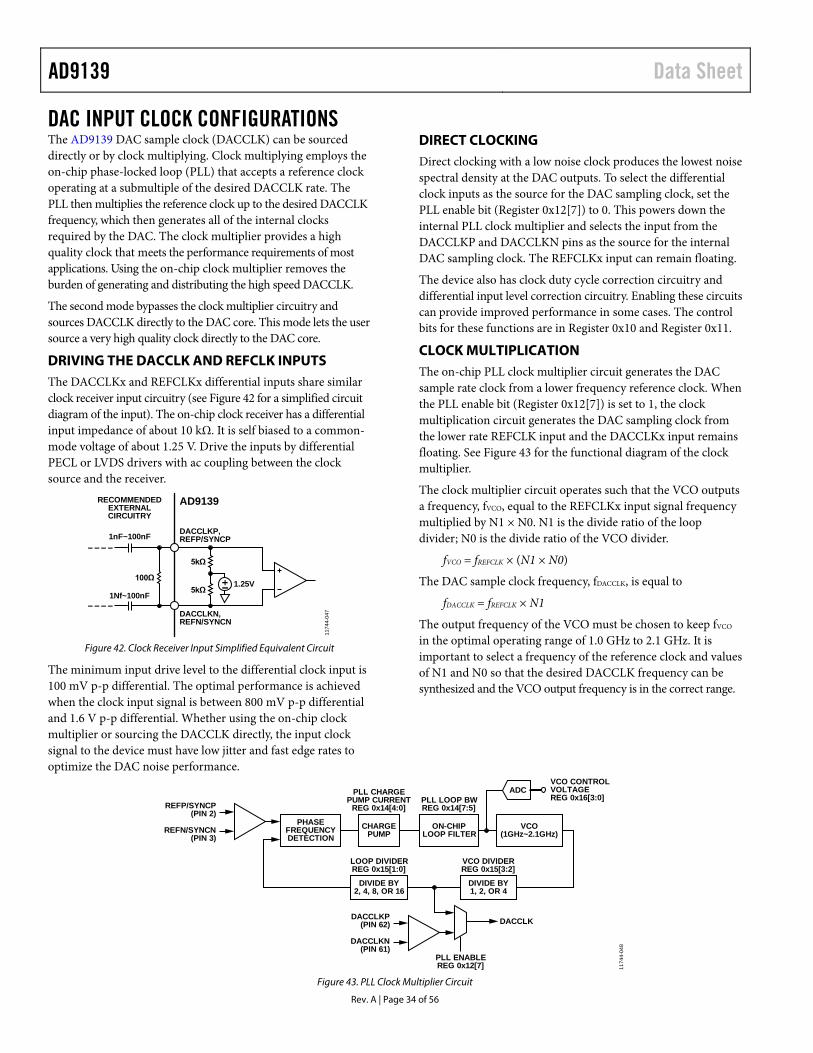
AD9139 Data Sheet
DAC INPUT CLOCK CONFIGURATIONS The AD9139 DAC sample clock (DACCLK) can be sourced directly or by clock multiplying. Clock multiplying employs the on-chip phase-locked loop (PLL) that accepts a reference clock operating at a submultiple of the desired DACCLK rate. The PLL then multiplies the reference clock up to the desired DACCLK frequency, which then generates all of the internal clocks required by the DAC. The clock multiplier provides a high quality clock that meets the performance requirements of most applications. Using the on-chip clock multiplier removes the burden of generating and distributing the high speed DACCLK.
The second mode bypasses the clock multiplier circuitry and sources DACCLK directly to the DAC core. This mode lets the user source a very high quality clock directly to the DAC core.
DRIVING THE DACCLK AND REFCLK INPUTS The DACCLKx and REFCLKx differential inputs share similar clock receiver input circuitry (see Figure 42 for a simplified circuit diagram of the input). The on-chip clock receiver has a differential input impedance of about 10 kΩ. It is self biased to a common-mode voltage of about 1.25 V. Drive the inputs by differential PECL or LVDS drivers with ac coupling between the clock source and the receiver.
Figure 42. Clock Receiver Input Simplified Equivalent Circuit
The minimum input drive level to the differential clock input is 100 mV p-p differential. The optimal performance is achieved when the clock input signal is between 800 mV p-p differential and 1.6 V p-p differential. Whether using the on-chip clock multiplier or sourcing the DACCLK directly, the input clock signal to the device must have low jitter and fast edge rates to optimize the DAC noise performance.
DIRECT CLOCKING Direct clocking with a low noise clock produces the lowest noise spectral density at the DAC outputs. To select the differential clock inputs as the source for the DAC sampling clock, set the PLL enable bit (Register 0x12[7]) to 0. This powers down the internal PLL clock multiplier and selects the input from the DACCLKP and DACCLKN pins as the source for the internal DAC sampling clock. The REFCLKx input can remain floating.
The device also has clock duty cycle correction circuitry and differential input level correction circuitry. Enabling these circuits can provide improved performance in some cases. The control bits for these functions are in Register 0x10 and Register 0x11.
CLOCK MULTIPLICATION The on-chip PLL clock multiplier circuit generates the DAC sample rate clock from a lower frequency reference clock. When the PLL enable bit (Register 0x12[7]) is set to 1, the clock multiplication circuit generates the DAC sampling clock from the lower rate REFCLK input and the DACCLKx input remains floating. See Figure 43 for the functional diagram of the clock multiplier.
The clock multiplier circuit operates such that the VCO outputs a frequency, fVCO, equal to the REFCLKx input signal frequency multiplied by N1 × N0. N1 is the divide ratio of the loop divider; N0 is the divide ratio of the VCO divider.
fVCO = fREFCLK × (N1 × N0)
The DAC sample clock frequency, fDACCLK, is equal to
fDACCLK = fREFCLK × N1
The output frequency of the VCO must be chosen to keep fVCO in the optimal operating range of 1.0 GHz to 2.1 GHz. It is important to select a frequency of the reference clock and values of N1 and N0 so that the desired DACCLK frequency can be synthesized and the VCO output frequency is in the correct range.
Figure 43. PLL Clock Multiplier Circuit
1.25V
5kΩ
100Ω5kΩ
DACCLKP,REFP/SYNCP
AD9139
DACCLKN,REFN/SYNCN
1nF~100nF
1Nf~100nF
RECOMMENDEDEXTERNALCIRCUITRY
1174
4-04
7
PHASEFREQUENCYDETECTION
CHARGEPUMP
PLL CHARGEPUMP CURRENT
REG 0x14[4:0]
DIVIDE BY2, 4, 8, OR 16
LOOP DIVIDERREG 0x15[1:0]
DIVIDE BY1, 2, OR 4
VCO DIVIDERREG 0x15[3:2]
ON-CHIPLOOP FILTER
PLL LOOP BWREG 0x14[7:5]
VCO(1GHz~2.1GHz)
ADCVCO CONTROLVOLTAGEREG 0x16[3:0]
REFP/SYNCP(PIN 2)
REFN/SYNCN(PIN 3)
DACCLKP(PIN 62)
DACCLKN(PIN 61)
DACCLK
PLL ENABLEREG 0x12[7] 11
744-
048
Rev. A | Page 34 of 56
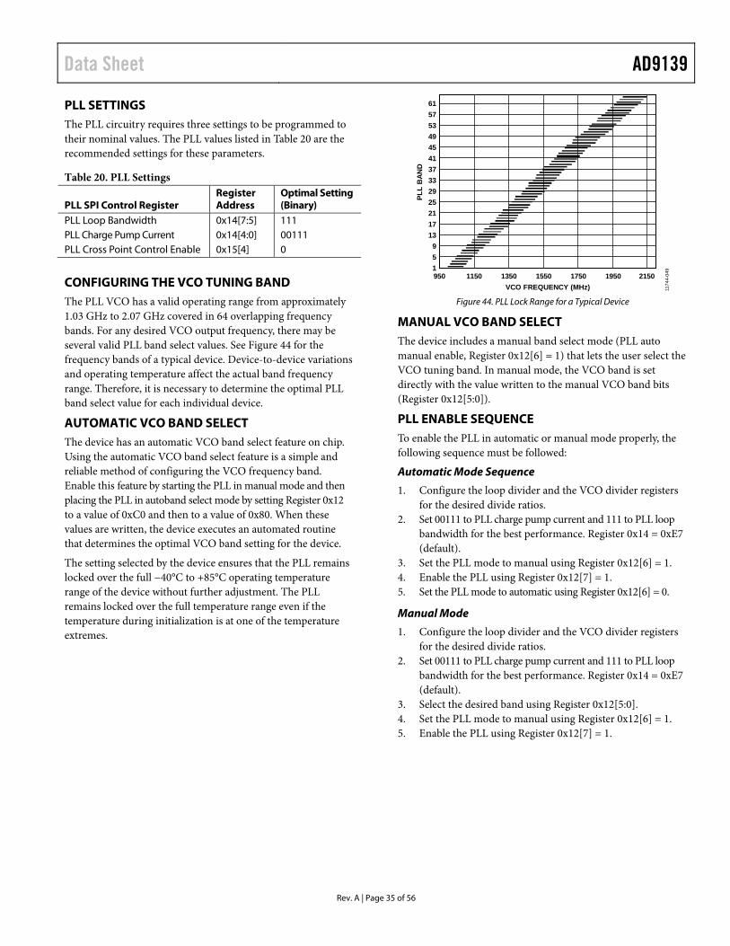
Data Sheet AD9139
Rev. A | Page 35 of 56
PLL SETTINGS The PLL circuitry requires three settings to be programmed to their nominal values. The PLL values listed in Table 20 are the recommended settings for these parameters.
Table 20. PLL Settings
PLL SPI Control Register Register Address
Optimal Setting (Binary)
PLL Loop Bandwidth 0x14[7:5] 111 PLL Charge Pump Current 0x14[4:0] 00111 PLL Cross Point Control Enable 0x15[4] 0
CONFIGURING THE VCO TUNING BAND The PLL VCO has a valid operating range from approximately 1.03 GHz to 2.07 GHz covered in 64 overlapping frequency bands. For any desired VCO output frequency, there may be several valid PLL band select values. See Figure 44 for the frequency bands of a typical device. Device-to-device variations and operating temperature affect the actual band frequency range. Therefore, it is necessary to determine the optimal PLL band select value for each individual device.
AUTOMATIC VCO BAND SELECT The device has an automatic VCO band select feature on chip. Using the automatic VCO band select feature is a simple and reliable method of configuring the VCO frequency band. Enable this feature by starting the PLL in manual mode and then placing the PLL in autoband select mode by setting Register 0x12 to a value of 0xC0 and then to a value of 0x80. When these values are written, the device executes an automated routine that determines the optimal VCO band setting for the device.
The setting selected by the device ensures that the PLL remains locked over the full −40°C to +85°C operating temperature range of the device without further adjustment. The PLL remains locked over the full temperature range even if the temperature during initialization is at one of the temperature extremes.
Figure 44. PLL Lock Range for a Typical Device
MANUAL VCO BAND SELECT The device includes a manual band select mode (PLL auto manual enable, Register 0x12[6] = 1) that lets the user select the VCO tuning band. In manual mode, the VCO band is set directly with the value written to the manual VCO band bits (Register 0x12[5:0]).
PLL ENABLE SEQUENCE To enable the PLL in automatic or manual mode properly, the following sequence must be followed:
Automatic Mode Sequence
1. Configure the loop divider and the VCO divider registers for the desired divide ratios.
2. Set 00111 to PLL charge pump current and 111 to PLL loop bandwidth for the best performance. Register 0x14 = 0xE7 (default).
3. Set the PLL mode to manual using Register 0x12[6] = 1. 4. Enable the PLL using Register 0x12[7] = 1. 5. Set the PLL mode to automatic using Register 0x12[6] = 0.
Manual Mode
1. Configure the loop divider and the VCO divider registers for the desired divide ratios.
2. Set 00111 to PLL charge pump current and 111 to PLL loop bandwidth for the best performance. Register 0x14 = 0xE7 (default).
3. Select the desired band using Register 0x12[5:0]. 4. Set the PLL mode to manual using Register 0x12[6] = 1. 5. Enable the PLL using Register 0x12[7] = 1.
61575349454137332925211713
951950 1150 1350 1550 1750 1950 2150
PLL
BA
ND
VCO FREQUENCY (MHz) 1174
4-04
9

AD9139 Data Sheet
ANALOG OUTPUTS TRANSMIT DAC OPERATION Figure 45 shows a simplified block diagram of the transmit path DACs. The DAC core consists of a current source array, a switch core, digital control logic, and full-scale output current control. The DAC full-scale output current (IOUTFS) is nominally 20 mA. The output currents from the DACOUTP and DACOUTN pins are complementary, meaning that the sum of the two currents always equals the full-scale current of the DAC. The digital input code to the DAC determines the effective differential current delivered to the load.
Figure 45. Simplified Block Diagram of DAC Core
The DAC has a 1.2 V band gap reference with an output imped-ance of 5 kΩ. The reference output voltage appears on the VREF pin. When using the internal reference, decouple the VREF pin to AVSS with a 0.1 µF capacitor. Use the internal reference only for external circuits that draw dc currents of 2 µA or less. For dynamic loads or static loads greater than 2 µA, buffer the VREF pin. If desired, the internal reference can be overdriven by applying an external reference (from 1.10 V to 1.30 V) to the pin.
A 10 kΩ external resistor, RSET, must be connected from the FSADJ pin to AVSS. This resistor, together with the reference control amplifier, sets up the correct internal bias currents for the DAC. Because the full-scale current is inversely proportional to this resistor, the tolerance of RSET is reflected in the full-scale output amplitude.
The full-scale current equation, where the DAC gain is set in Register 0x18 and Register 0x19, is as follows:
×+×= DAC gain
RV
ISET
REFFS 16
372
For nominal values of VREF (1.2 V), RSET (10 kΩ), and DAC gain (512), the full-scale current of the DAC is typically 20 mA. The DAC full-scale current is adjustable from 8.64 mA to 31.68 mA by setting the DAC gain parameter, as shown in Figure 46.
Figure 46. DAC Full-Scale Current vs. DAC Gain Code
Transmit DAC Transfer Function
The output currents from the DACOUTP and DACOUTN pins are complementary, meaning that the sum of the two currents always equals the full-scale current of the DAC. The digital input code to the DAC determines the effective differential current delivered to the load. The DACOUTP pin provides maximum output current when all bits are high. The output currents vs. DACCODE for the DAC outputs is expressed as
OUTFSNOUTP IDACCODEI ×
=
2 (1)
IOUTN = IOUTFS – IOUTP (2)
where DACCODE = 0 to 2N − 1.
Transmit DAC Output Configurations
The optimum noise and distortion performance of the AD9139 is realized when it is configured for differential operation. The common-mode rejection of a transformer or differential amplifier significantly reduces the common-mode error sources of the DAC outputs. These common-mode error sources include even-order distortion products and noise. The enhancement in distortion performance becomes more significant as the frequency content of the reconstructed waveform increases and/or its amplitude increases. This is due to the first-order cancellation of various dynamic common-mode distortion mechanisms, digital feed-through, and noise.
Figure 47 shows the most basic DAC output circuitry. A pair of resistors, RO, converts each of the complementary output currents to a differential voltage output, VOUT. Because the current outputs of the DAC are high impedance, the differential driving point impedance of the DAC outputs, ROUT, is equal to 2 × RO. See Figure 48 for the output voltage waveforms.
DACDACOUTP
DACOUTN
CURRENTSCALING
DAC FSADJUSTREG 0x18, 0x19
0.1µF
10kΩRSET
FSADJ
VREF5kΩ
1.2V
1174
4-05
0
35
00 1000
DAC GAIN CODE
I FS
(mA
)
30
25
20
15
10
5
200 400 600 800
1 174
4-05
1
Rev. A | Page 36 of 56

Data Sheet AD9139
Figure 47. Basic Transmit DAC Output Circuit
Figure 48. Output Voltage Waveforms
The common-mode signal voltage, VCM, is calculated as
OFS
CM RI
V ×=2
The differential peak-to-peak output voltage, VPEAK, is calculated as
VPEAK = 2 × IFS × RO
INTERFACING TO MODULATORS The AD9139 interfaces to the ADL537x family of modulators with a minimal number of components. An example of the recommended interface circuitry is shown in Figure 49.
Figure 49. Typical Interface Circuitry Between the AD9139 and the ADL537x
Family of Modulators
The baseband inputs of the ADL537x family require a dc bias of 500 mV. The nominal midscale output current on each output of the DAC is 10 mA (one-half the full-scale current). Therefore, a single 50 Ω resistor to ground from each of the DAC outputs results in the desired 500 mV dc common-mode bias for the inputs to the ADL537x. The addition of the load resistor in parallel with the modulator inputs reduces the signal level. The peak-to-peak voltage swing of the transmitted signal is
)2()2(
LB
LBFSSIGNAL RR
RRIV
+×
×××=
Baseband Filter Implementation
Most applications require a baseband anti-imaging filter between the DAC and the modulator to filter out Nyquist images and broadband DAC noise. The filter can be inserted between the termination resistors at the DAC output and the signal level setting resistor across the modulator input. This configuration establishes the input and output impedances for the filter.
Figure 50 shows a fifth-order, low-pass filter. Splitting the filter capacitors into two and grounding the center point creates a common-mode low-pass filter that provides additional common-mode rejection of high frequency signals. A purely differential filter can pass common-mode signals.
For more details about interfacing the AD9139 DAC to an IQ modulator,see the Circuits from the Lab™, Circuit Note CN-0205, Interfacing the ADL5375 I/Q Modulator to the AD9122 Dual Channel, 1.2 GSPS High Speed DAC on the Analog Devices website.
Figure 50. DAC Modulator Interface with Fifth-Order, Low-Pass Filter
RO
RO
VOUTP +
VOUTN –
VOUT
DACOUTP
DACOUTN
1174
4-05
2
+VPEAK
VCM
0
–VPEAK
VN VP
VOUT
1174
4-05
3
RBIP50Ω
RBIN50Ω
67
66IBBN
IBBP
AD9139 ADL537x
RBQN50Ω
RBQP50Ω
67
66
RLI100Ω
RLQ100Ω
DACOUTN
DACOUTP
DACOUTN
DACOUTPAD9139
QBBP
QBBN
1174
4-05
4
AD9139
50Ω
50Ω33nH
33nH3.6pF
33nH
33nH140Ω6pF
3pF
3pF
22pF
22pF
ADL537x
1174
4-05
5
Rev. A | Page 37 of 56

AD9139 Data Sheet
REDUCING LO LEAKAGE AND UNWANTED SIDEBANDS Analog quadrature modulators can introduce unwanted signals at the local oscillator (LO) frequency caused by dc offset voltages in the I and Q baseband inputs, as well as feedthrough paths from the LO input to the output.
Effective sideband suppression requires both gain and phase matching of the I and Q signals. The DAC FS adjust registers
(Register 0x18 through Register 0x19) can be used to calibrate the gain of the transmit paths to optimize sideband suppression.
For more information about suppressing LO leakage and sideband image, refer to Application Note AN-1039, Correcting Imperfections in IQ Modulators to Improve RF Signal Fidelity and Application Note AN-1100, Wireless Transmitter IQ Balance and Sideband Suppression from the Analog Devices website.
Rev. A | Page 38 of 56
Data Sheet AD9139
START-UP ROUTINE To ensure reliable start up of the AD9139, certain sequences must be followed.
Device Configuration and Start-Up Sequence 1
1. Set fDCI = 600 MHz, fDATA = 1200 MHz, and interpolation to 1×. 2. Enable the PLL, and set fREF = 300 MHz. 3. Enable the inverse sinc filter. 4. Use the DLL-based interface mode and set DLL phase
offset = 0.
Derived PLL Settings
The following PLL settings are derived from the device configuration:
• fDAC = 1200 × 1 = 1200 MHz. • fVCO= fDAC = 1200 MHz (1 GHz < fVCO < 2 GHz). • VCO divider = fVCO/fDAC = 1. • Loop divider = fDAC/fREF = 4.
Start-Up Sequence 1
1. Power up the device (no specific power supply sequence is required).
2. Apply stable DAC clock. 3. Apply stable DCI clock. 4. Feed stable input data. 5. Issue hardware reset (optional).
/* Device configuration register write sequence */
0x00 → 0x20 /* Issue software reset */
0x20 → 0x01 /* Device Startup Configuration */
/* Configure PLL */
0x14 → 0xE7 /* Configure PLL loop BW and charge pump current */
0x15 → 0xC1 /* Configure VCO divider and loop divider */
0x12 → 0xC0 /*Enable the PLL */
0x12 → 0x80
Wait 10ms
Read 0x16[7] /* Expect 1b if the PLL is locked */
/* Configure Data Interface */
0x5E → 0xFE /* Turn off LSB delay cell */
0x0A → 0xC0 /* Enable the DLL and duty cycle correction. Set DLL phase offset to 0 */
Read 0x0E[7:4] /* Expect 1000b if the DLL is locked */
/* Configure Interpolation filter */
0x28 → 0x80 /* 1× interpolation */
/* Reset FIFO */
0x25 → 0x01
Read 0x25[1] /* Expect 1b if the FIFO reset is complete */
Read 0x24 /* The readback should be one of the three values: 0x30, 0x40, or 0x50 */
/* Enable Inverse SINC filter */
0x27 → 0x80
/* Power up DAC outputs */
0x01 → 0x00
Device Configuration and Start-Up Sequence 2
1. Set fDCI = 200 MHz, fDATA = 400 MHz, fDAC = 800 MHz, and interpolation to 2×.
2. Disable PLL. 3. Enable the inverse sinc filter. 4. Use the delay line-based interface mode with a delay
setting of 0.
Start-Up Sequence 2
1. Power up the device (no specific power supply sequence is required).
2. Apply stable DAC clock. 3. Apply stable DCI clock. 4. Feed stable input data. 5. Issue a hardware reset (optional).
/* Device configuration register write sequence */
0x00 → 0x20 /* Issue software reset */
0x20 → 0x01 /* Device Startup Configuration */
/* Configure Data Interface */
0x5E → 0x00 /* Configure the delay setting */
0x5F → 0x60
0x0D → 0x16 /* DC couple DCI */
0x0A → 0x00 /* Turn off DLL and duty cycle correction */
/* Configure Interpolation filter */
0x28 → 0x00 /* 2× interpolation */
/* Reset FIFO */
Follow the serial port FIFO reset procedure in the FIFO Operation section.
/* Enable Inverse SINC filter */
0x27 → 0x80
/* Power up DAC outputs */
0x01 → 0x00
Rev. A | Page 39 of 56
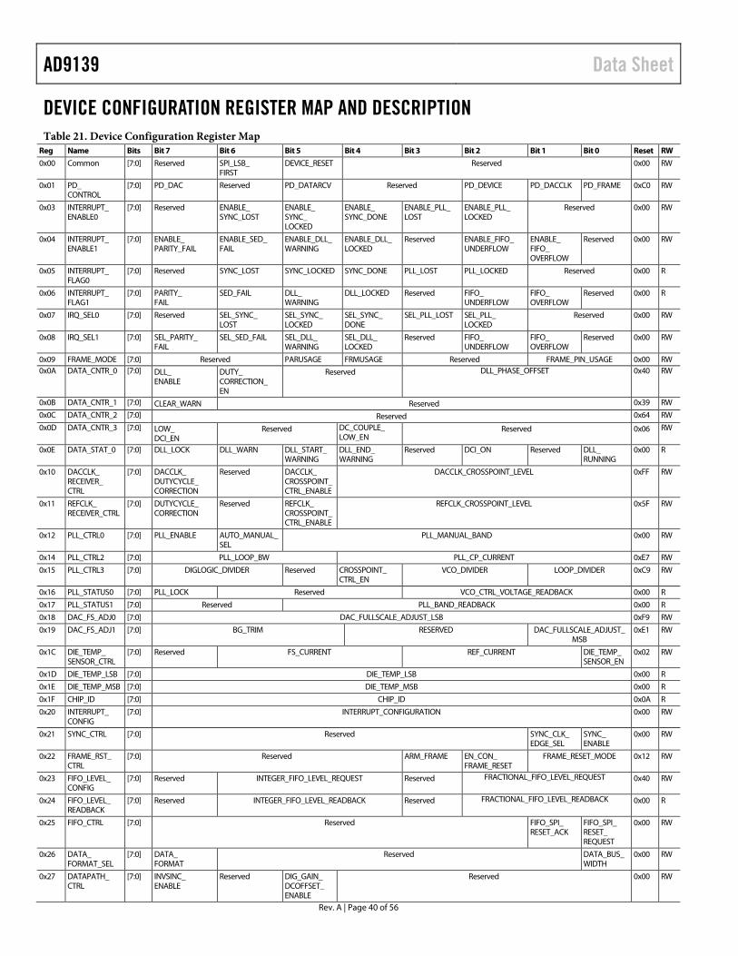
AD9139 Data Sheet
DEVICE CONFIGURATION REGISTER MAP AND DESCRIPTION Table 21. Device Configuration Register Map
Reg Name Bits Bit 7 Bit 6 Bit 5 Bit 4 Bit 3 Bit 2 Bit 1 Bit 0 Reset RW
0x00 Common [7:0] Reserved SPI_LSB_ FIRST
DEVICE_RESET Reserved 0x00 RW
0x01 PD_ CONTROL
[7:0] PD_DAC Reserved PD_DATARCV Reserved PD_DEVICE PD_DACCLK PD_FRAME 0xC0 RW
0x03 INTERRUPT_ ENABLE0
[7:0] Reserved ENABLE_ SYNC_LOST
ENABLE_ SYNC_ LOCKED
ENABLE_ SYNC_DONE
ENABLE_PLL_ LOST
ENABLE_PLL_ LOCKED
Reserved 0x00 RW
0x04 INTERRUPT_ ENABLE1
[7:0] ENABLE_ PARITY_FAIL
ENABLE_SED_ FAIL
ENABLE_DLL_ WARNING
ENABLE_DLL_ LOCKED
Reserved ENABLE_FIFO_ UNDERFLOW
ENABLE_ FIFO_ OVERFLOW
Reserved 0x00 RW
0x05 INTERRUPT_ FLAG0
[7:0] Reserved SYNC_LOST SYNC_LOCKED SYNC_DONE PLL_LOST PLL_LOCKED Reserved 0x00 R
0x06 INTERRUPT_ FLAG1
[7:0] PARITY_ FAIL
SED_FAIL DLL_ WARNING
DLL_LOCKED Reserved FIFO_ UNDERFLOW
FIFO_ OVERFLOW
Reserved 0x00 R
0x07 IRQ_SEL0 [7:0] Reserved SEL_SYNC_ LOST
SEL_SYNC_ LOCKED
SEL_SYNC_ DONE
SEL_PLL_LOST SEL_PLL_ LOCKED
Reserved 0x00 RW
0x08 IRQ_SEL1 [7:0] SEL_PARITY_ FAIL
SEL_SED_FAIL SEL_DLL_ WARNING
SEL_DLL_ LOCKED
Reserved FIFO_ UNDERFLOW
FIFO_ OVERFLOW
Reserved 0x00 RW
0x09 FRAME_MODE [7:0] Reserved PARUSAGE FRMUSAGE Reserved FRAME_PIN_USAGE 0x00 RW 0x0A DATA_CNTR_0 [7:0] DLL_
ENABLE DUTY_ CORRECTION_ EN
Reserved DLL_PHASE_OFFSET 0x40 RW
0x0B DATA_CNTR_1 [7:0] CLEAR_WARN Reserved 0x39 RW
0x0C DATA_CNTR_2 [7:0] Reserved 0x64 RW
0x0D DATA_CNTR_3 [7:0] LOW_ DCI_EN
Reserved DC_COUPLE_ LOW_EN
Reserved 0x06 RW
0x0E DATA_STAT_0 [7:0] DLL_LOCK DLL_WARN DLL_START_ WARNING
DLL_END_ WARNING
Reserved DCI_ON Reserved DLL_ RUNNING
0x00 R
0x10 DACCLK_ RECEIVER_ CTRL
[7:0] DACCLK_ DUTYCYCLE_ CORRECTION
Reserved DACCLK_ CROSSPOINT_ CTRL_ENABLE
DACCLK_CROSSPOINT_LEVEL 0xFF RW
0x11 REFCLK_ RECEIVER_CTRL
[7:0] DUTYCYCLE_ CORRECTION
Reserved REFCLK_ CROSSPOINT_ CTRL_ENABLE
REFCLK_CROSSPOINT_LEVEL 0x5F RW
0x12 PLL_CTRL0 [7:0] PLL_ENABLE AUTO_MANUAL_SEL
PLL_MANUAL_BAND 0x00 RW
0x14 PLL_CTRL2 [7:0] PLL_LOOP_BW PLL_CP_CURRENT 0xE7 RW
0x15 PLL_CTRL3 [7:0] DIGLOGIC_DIVIDER Reserved CROSSPOINT_ CTRL_EN
VCO_DIVIDER LOOP_DIVIDER 0xC9 RW
0x16 PLL_STATUS0 [7:0] PLL_LOCK Reserved VCO_CTRL_VOLTAGE_READBACK 0x00 R
0x17 PLL_STATUS1 [7:0] Reserved PLL_BAND_READBACK 0x00 R
0x18 DAC_FS_ADJ0 [7:0] DAC_FULLSCALE_ADJUST_LSB 0xF9 RW
0x19 DAC_FS_ADJ1 [7:0] BG_TRIM RESERVED DAC_FULLSCALE_ADJUST_ MSB
0xE1 RW
0x1C DIE_TEMP_ SENSOR_CTRL
[7:0] Reserved FS_CURRENT REF_CURRENT DIE_TEMP_ SENSOR_EN
0x02 RW
0x1D DIE_TEMP_LSB [7:0] DIE_TEMP_LSB 0x00 R
0x1E DIE_TEMP_MSB [7:0] DIE_TEMP_MSB 0x00 R
0x1F CHIP_ID [7:0] CHIP_ID 0x0A R
0x20 INTERRUPT_ CONFIG
[7:0] INTERRUPT_CONFIGURATION 0x00 RW
0x21 SYNC_CTRL [7:0] Reserved SYNC_CLK_ EDGE_SEL
SYNC_ ENABLE
0x00 RW
0x22 FRAME_RST_ CTRL
[7:0] Reserved ARM_FRAME EN_CON_ FRAME_RESET
FRAME_RESET_MODE 0x12 RW
0x23 FIFO_LEVEL_ CONFIG
[7:0] Reserved INTEGER_FIFO_LEVEL_REQUEST Reserved FRACTIONAL_FIFO_LEVEL_REQUEST 0x40 RW
0x24 FIFO_LEVEL_ READBACK
[7:0] Reserved INTEGER_FIFO_LEVEL_READBACK Reserved FRACTIONAL_FIFO_LEVEL_READBACK 0x00 R
0x25 FIFO_CTRL [7:0] Reserved FIFO_SPI_ RESET_ACK
FIFO_SPI_ RESET_ REQUEST
0x00 RW
0x26 DATA_ FORMAT_SEL
[7:0] DATA_ FORMAT
Reserved DATA_BUS_ WIDTH
0x00 RW
0x27 DATAPATH_ CTRL
[7:0] INVSINC_ ENABLE
Reserved DIG_GAIN_ DCOFFSET_ ENABLE
Reserved 0x00 RW
Rev. A | Page 40 of 56

Data Sheet AD9139
Reg Name Bits Bit 7 Bit 6 Bit 5 Bit 4 Bit 3 Bit 2 Bit 1 Bit 0 Reset RW
0x28 INTERPOLATION_CTRL
[7:0] INTERPOLATION_ MODE
0x00 RW
0x39 LVDS_IN_PWR_DOWN_0
[7:0] Reserved PWR_DOWN_DATA_INPUT_BITS 0x00 RW
0x3B DAC_DC_ OFFSET0
[7:0] DAC_DC_OFFSET_LSB 0x00 RW
0x3C DAC_DC_ OFFSET1
[7:0] DAC_DC_OFFSET_MSB 0x00 RW
0x3F DAC_DIG_GAIN [7:0] Reserved DAC_DIG_GAIN 0x20 RW
0x41 GAIN_STEP_ CTRL0
[7:0] Reserved RAMP_UP_STEP 0x01 RW
0x42 GAIN_STEP_ CTRL1
[7:0] DAC_OUTPUT_ STATUS
DAC_OUTPUT_ ON
RAMP_DOWN_STEP 0x01 RW
0x43 TX_ENABLE_ CTRL
[7:0] Reserved TXENABLE_ GAINSTEP_ EN
TXENABLE_ SLEEP_ EN
TXENABLE_POWER_ DOWN_EN
0x07 RW
0x44 DAC_ OUTPUT_ CTRL
[7:0] DAC_OUTPUT_ CTRL_EN
Reserved FIFO_WARNING_SHUTDOWN_EN
Reserved FIFO_ ERROR_ SHUTDOWN_EN
0x8F RW
0x5E ENABLE_DLL_ DELAY_CELL0
[7:0] ENABLE_DLL_DELAY_CELL[7:0] 0xFF
0x5F ENABLE_DLL_ DELAY_CELL1
[7:0] Reserved ENABLE_DLL_DELAY_CELL[10:8] 0x67 RW
0x60 SED_CTRL [7:0] SED_ENABLE SED_ERR_CLEAR AED_ENABLE SED_DEPTH Reserved AED_PASS AED_FAIL SED_FAIL 0x00 RW
0x61 SED_PATT_ L_S0
[7:0] SED_PATTERN_RISE_S0 [7:0] 0x00 RW
0x62 SED_PATT_ H_S0
[7:0] SED_PATTERN_RISE_S0 [15:8] 0x00 RW
0x63 SED_PATT_ L_S1
[7:0] SED_PATTERN_FALL_S1 [7:0] 0x00 RW
0x64 SED_PATT_ H_S1
[7:0] SED_PATTERN_FALL_S1 [15:8] 0x00 RW
0x65 SED_PATT_ L_S2
[7:0] SED_PATTERN_RISE_S2 [7:0] 0x00 RW
0x66 SED_PATT_ H_S2
[7:0] SED_PATTERN_RISE_S2 [15:8] 0x00 RW
0x67 SED_PATT_ L S3
[7:0] SED_PATTERN_FALL_S3 [7:0] 0x00 RW
0x68 SED_PATT_ H_S3
[7:0] SED_PATTERN_FALL_S3 [15:8] 0x00 RW
0x6A PARITY_CTRL [7:0] PARITY_ENABLE PARITY_EVEN PARITY_ ERR_CLEAR
Reserved PARERRFAL PARERRRIS 0x00 RW
0x6B PARITY_ ERR_RISING
[7:0] PARITY RISING EDGE ERROR COUNT 0x00 R
0x6C PARITY_ ERR_FALLING
[7:0] PARITY FALLING EDGE ERROR COUNT 0x00 R
0x7F Version [7:0] Version 0x0B R
Rev. A | Page 41 of 56

AD9139 Data Sheet
Rev. A | Page 42 of 56
SPI CONFIGURE REGISTER Address: 0x00, Reset: 0x00, Name: Common
Table 22. Bit Descriptions for Common Bit No. Bit Name Settings Description Reset Access 6 SPI_LSB_FIRST Serial port communication, MSB first or LSB first selection. 0 R/W
0 MSB first. 1 LSB first.
5 DEVICE_RESET The device resets when 1 is written to this bit. DEVICE_RESET is a self clear bit. After the reset, the bit returns to 0 automatically. The readback is always 0.
0 R/W
POWER-DOWN CONTROL REGISTER Address: 0x01, Reset: 0xC0, Name: PD_CONTROL
Table 23. Bit Descriptions for PD_CONTROL Bit No. Bit Name Settings Description Reset Access 7 PD_DAC The DAC is powered down when PD_DAC is set to 1. This bit powers down only the
analog portion of the DAC. The DAC digital data path is not affected. 1 R/W
6 Reserved Must set to default value. 1 R/W 5 PD_DATARCV The data interface circuitry is powered down when PD_DATARCV is set to 1. This bit
powers down the data interface and the write side of the FIFO. 0 R/W
2 PD_DEVICE The band gap circuitry is powered down when set to 1. This bit powers down the entire chip.
0 R/W
1 PD_DACCLK The DAC clock powers down when PD_DEVICE is set to 1. This bit powers down the DAC clocking path and, thus, the majority of the digital functions.
0 R/W
0 PD_FRAME The frame receiver powers down when PD_FRAME is set to 1. The frame signal is internally pulled low. Set to 1 when frame is not used.
0 R/W
INTERRUPT ENABLE 0 REGISTER Address: 0x03, Reset: 0x00, Name: INTERRUPT_ENABLE0
Table 24. Bit Descriptions for INTERRUPT_ENABLE0 Bit No. Bit Name Settings Description Reset Access 6 ENABLE_SYNC_LOST Enable interrupt for sync lost. 0 R/W 5 ENABLE_SYNC_LOCKED Enable interrupt for sync lock. 0 R/W 4 ENABLE_SYNC_DONE Enable interrupt for sync done. 0 R/W 3 ENABLE_PLL_LOST Enable interrupt for PLL lost. 0 R/W 2 ENABLE_PLL_LOCKED Enable interrupt for PLL locked. 0 R/W
INTERRUPT ENABLE 1 REGISTER Address: 0x04, Reset: 0x00, Name: INTERRUPT_ENABLE1
Table 25. Bit Descriptions for INTERRUPT_ENABLE1 Bit No. Bit Name Settings Description Reset Access 7 ENABLE_PARITY_FAIL Enable interrupt for parity failure. 0 R/W 6 ENABLE_SED_FAIL Enable interrupt for SED failure. 0 R/W 5 ENABLE_DLL_WARNING Enable interrupt for DLL warning. 0 R/W 4 ENABLE_DLL_LOCKED Enable interrupt for DLL locked. 0 R/W 2 ENABLE_FIFO_UNDERFLOW Enable interrupt for FIFO underflow. 0 R/W 1 ENABLE_FIFO_OVERFLOW Enable interrupt for FIFO overflow. 0 R/W
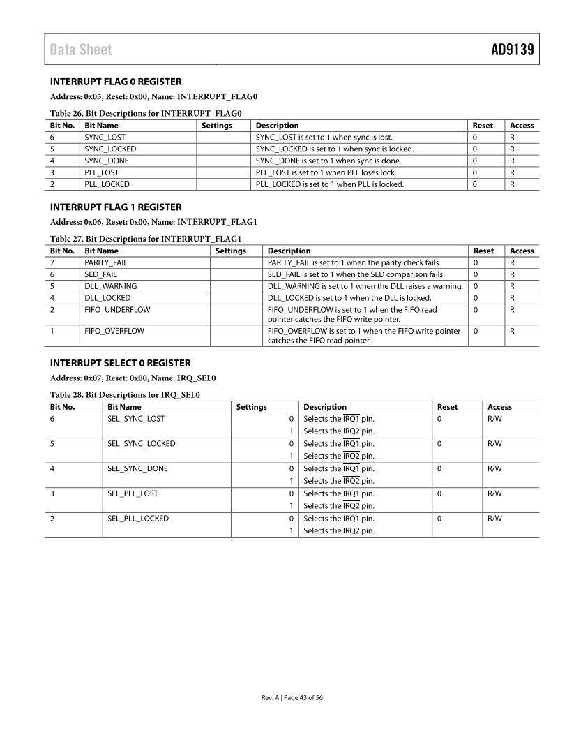
Data Sheet AD9139
INTERRUPT FLAG 0 REGISTER Address: 0x05, Reset: 0x00, Name: INTERRUPT_FLAG0
Table 26. Bit Descriptions for INTERRUPT_FLAG0 Bit No. Bit Name Settings Description Reset Access 6 SYNC_LOST SYNC_LOST is set to 1 when sync is lost. 0 R 5 SYNC_LOCKED SYNC_LOCKED is set to 1 when sync is locked. 0 R 4 SYNC_DONE SYNC_DONE is set to 1 when sync is done. 0 R 3 PLL_LOST PLL_LOST is set to 1 when PLL loses lock. 0 R 2 PLL_LOCKED PLL_LOCKED is set to 1 when PLL is locked. 0 R
INTERRUPT FLAG 1 REGISTER Address: 0x06, Reset: 0x00, Name: INTERRUPT_FLAG1
Table 27. Bit Descriptions for INTERRUPT_FLAG1 Bit No. Bit Name Settings Description Reset Access 7 PARITY_FAIL PARITY_FAIL is set to 1 when the parity check fails. 0 R 6 SED_FAIL SED_FAIL is set to 1 when the SED comparison fails. 0 R 5 DLL_WARNING DLL_WARNING is set to 1 when the DLL raises a warning. 0 R 4 DLL_LOCKED DLL_LOCKED is set to 1 when the DLL is locked. 0 R 2 FIFO_UNDERFLOW FIFO_UNDERFLOW is set to 1 when the FIFO read
pointer catches the FIFO write pointer. 0 R
1 FIFO_OVERFLOW FIFO_OVERFLOW is set to 1 when the FIFO write pointer catches the FIFO read pointer.
0 R
INTERRUPT SELECT 0 REGISTER Address: 0x07, Reset: 0x00, Name: IRQ_SEL0
Table 28. Bit Descriptions for IRQ_SEL0 Bit No. Bit Name Settings Description Reset Access 6 SEL_SYNC_LOST 0 Selects the IRQ1 pin. 0 R/W
1 Selects the IRQ2 pin.
5 SEL_SYNC_LOCKED 0 Selects the IRQ1 pin. 0 R/W
1 Selects the IRQ2 pin.
4 SEL_SYNC_DONE 0 Selects the IRQ1 pin. 0 R/W
1 Selects the IRQ2 pin.
3 SEL_PLL_LOST 0 Selects the IRQ1 pin. 0 R/W
1 Selects the IRQ2 pin.
2 SEL_PLL_LOCKED 0 Selects the IRQ1 pin. 0 R/W
1 Selects the IRQ2 pin.
Rev. A | Page 43 of 56
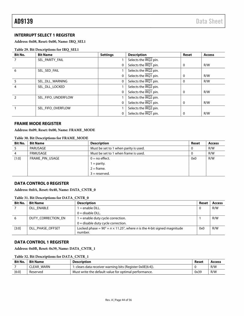
AD9139 Data Sheet
INTERRUPT SELECT 1 REGISTER Address: 0x08, Reset: 0x00, Name: IRQ_SEL1
Table 29. Bit Descriptions for IRQ_SEL1 Bit No. Bit Name Settings Description Reset Access 7 SEL_PARITY_FAIL 1 Selects the IRQ2 pin.
0 Selects the IRQ1 pin. 0 R/W
6 SEL_SED_FAIL 1 Selects the IRQ2 pin.
0 Selects the IRQ1 pin. 0 R/W
5 SEL_DLL_WARNING 0 Selects the IRQ1 pin. 0 R/W
4 SEL_DLL_LOCKED 1 Selects the IRQ2 pin.
0 Selects the IRQ1 pin. 0 R/W
2 SEL_FIFO_UNDERFLOW 1 Selects the IRQ2 pin.
0 Selects the IRQ1 pin. 0 R/W
1 SEL_FIFO_OVERFLOW 1 Selects the IRQ2 pin.
0 Selects the IRQ1 pin. 0 R/W
FRAME MODE REGISTER Address: 0x09, Reset: 0x00, Name: FRAME_MODE
Table 30. Bit Descriptions for FRAME_MODE Bit No. Bit Name Description Reset Access 5 PARUSAGE Must be set to 1 when parity is used. 0 R/W 4 FRMUSAGE Must be set to 1 when frame is used. 0 R/W [1:0] FRAME_PIN_USAGE 0 = no effect. 0x0 R/W
1 = parity. 2 = frame. 3 = reserved.
DATA CONTROL 0 REGISTER Address: 0x0A, Reset: 0x40, Name: DATA_CNTR_0
Table 31. Bit Descriptions for DATA_CNTR_0 Bit No. Bit Name Description Reset Access 7 DLL_ENABLE 1 = enable DLL. 0 R/W
0 = disable DLL. 6 DUTY_CORRECTION_EN 1 = enable duty cycle correction. 1 R/W
0 = disable duty cycle correction. [3:0] DLL_PHASE_OFFSET Locked phase = 90° + n × 11.25°, where n is the 4-bit signed magnitude
number. 0x0 R/W
DATA CONTROL 1 REGISTER Address: 0x0B, Reset: 0x39, Name: DATA_CNTR_1
Table 32. Bit Descriptions for DATA_CNTR_1 Bit No. Bit Name Description Reset Access 7 CLEAR_WARN 1: clears data receiver warning bits (Register 0x0E[6:4]). 0 R/W [6:0] Reserved Must write the default value for optimal performance. 0x39 R/W
Rev. A | Page 44 of 56
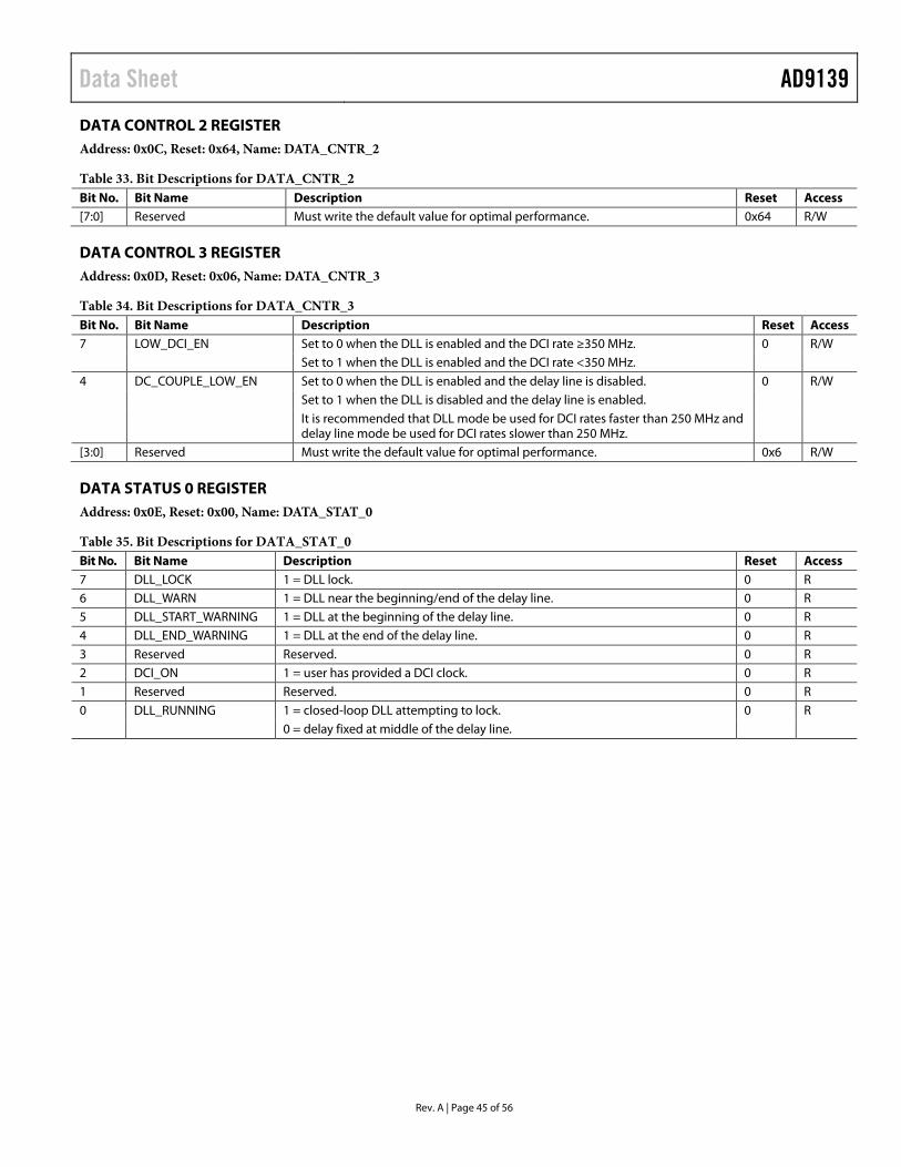
Data Sheet AD9139
DATA CONTROL 2 REGISTER Address: 0x0C, Reset: 0x64, Name: DATA_CNTR_2
Table 33. Bit Descriptions for DATA_CNTR_2 Bit No. Bit Name Description Reset Access [7:0] Reserved Must write the default value for optimal performance. 0x64 R/W
DATA CONTROL 3 REGISTER Address: 0x0D, Reset: 0x06, Name: DATA_CNTR_3
Table 34. Bit Descriptions for DATA_CNTR_3 Bit No. Bit Name Description Reset Access 7 LOW_DCI_EN Set to 0 when the DLL is enabled and the DCI rate ≥350 MHz. 0 R/W
Set to 1 when the DLL is enabled and the DCI rate <350 MHz. 4 DC_COUPLE_LOW_EN Set to 0 when the DLL is enabled and the delay line is disabled. 0 R/W
Set to 1 when the DLL is disabled and the delay line is enabled. It is recommended that DLL mode be used for DCI rates faster than 250 MHz and delay line mode be used for DCI rates slower than 250 MHz.
[3:0] Reserved Must write the default value for optimal performance. 0x6 R/W
DATA STATUS 0 REGISTER Address: 0x0E, Reset: 0x00, Name: DATA_STAT_0
Table 35. Bit Descriptions for DATA_STAT_0 Bit No. Bit Name Description Reset Access 7 DLL_LOCK 1 = DLL lock. 0 R 6 DLL_WARN 1 = DLL near the beginning/end of the delay line. 0 R 5 DLL_START_WARNING 1 = DLL at the beginning of the delay line. 0 R 4 DLL_END_WARNING 1 = DLL at the end of the delay line. 0 R 3 Reserved Reserved. 0 R 2 DCI_ON 1 = user has provided a DCI clock. 0 R 1 Reserved Reserved. 0 R 0 DLL_RUNNING
1 = closed-loop DLL attempting to lock. 0 R 0 = delay fixed at middle of the delay line.
Rev. A | Page 45 of 56
AD9139 Data Sheet
DAC CLOCK RECEIVER CONTROL REGISTER Address: 0x10, Reset: 0xFF, Name: DACCLK_RECEIVER_CTRL
Table 36. Bit Descriptions for DACCLK_RECEIVER_CTRL Bit No. Bit Name Settings Description Reset Access 7 DACCLK_DUTYCYCLE_CORRECTION Enables duty cycle correction at the DACCLK input. For
best performance, the default and recommended status is turned on.
1 R/W
6 Reserved Must write the default value for optimal performance 1 R/W 5 DACCLK_CROSSPOINT_CTRL_ENABLE Enables crosspoint control at the DACCLK input. For best
performance, the default and recommended status is turned on.
1 R/W
[4:0] DACCLK_CROSSPOINT_LEVEL A twos complement value. For best performance, set the DACCLK_CROSSPOINT_LEVEL to the default value.
0x1F R/W
01111 Highest crosspoint. 11111 Lowest crosspoint.
REFERENCE CLOCK RECEIVER CONTROL REGISTER Address: 0x11, Reset: 0x5F, Name: REFCLK_RECEIVER_CTRL
Table 37. Bit Descriptions for REFCLK_RECEIVER_CTRL Bit No. Bit Name Settings Description Reset Access 7 DUTYCYCLE_CORRECTION Enables duty cycle correction at the REFCLK input. For best
performance, the default and recommended status is turned off.
0 RW
6 Reserved Must write the default value for optimal performance. 1 R/W 5 REFCLK_CROSSPOINT_CTRL_ENABLE Enables crosspoint control at the REFCLK input. For best
performance, the default and recommended status is turned off.
0 RW
[4:0] REFCLK_CROSSPOINT_LEVEL A twos complement value. For best performance, set REFCLK_CROSSPOINT_LEVEL to the default value.
0x1F RW
01111 Highest crosspoint. 11111 Lowest crosspoint.
PLL CONTROL 0 REGISTER Address: 0x12, Reset: 0x00, Name: PLL_CTRL0
Table 38. Bit Descriptions for PLL_CTRL0 Bit No. Bit Name Settings Description Reset Access 7 PLL_ENABLE Enables PLL clock multiplier. 0 R/W 6 AUTO_MANUAL_SEL PLL band selection mode. 0 R/W 0 Automatic mode. 1 Manual mode. [5:0] PLL_MANUAL_BAND PLL band setting in manual mode. 64 bands in total, covering a 1 GHz to
2.1 GHz VCO range. 0x00 R/W
000000 Lowest band (1.03 GHz). 111111 Highest band (2.07 GHz).
Rev. A | Page 46 of 56
Data Sheet AD9139
PLL CONTROL 2 REGISTER Address: 0x14, Reset: 0xE7, Name: PLL_CTRL2
Table 39. Bit Descriptions for PLL_CTRL2 Bit No. Bit Name Settings Description Reset Access [7:5] PLL_LOOP_BW Selects the PLL loop filter bandwidth. The default and recommended
setting is 111 for optimal PLL performance. 0x7 R/W
0x00 Lowest setting. 0x1F Highest setting. [4:0] PLL_CP_CURRENT Sets nominal PLL charge pump current. The default and
recommended setting is 00111 for optimal PLL performance. 0x07 R/W
0x00 Lowest setting. 0x1F Highest setting.
PLL CONTROL 3 REGISTER Address: 0x15, Reset: 0xC9, Name: PLL_CTRL3
Table 40. Bit Descriptions for PLL_CTRL3 Bit No. Bit Name Settings Description Reset Access [7:6] DIGLOGIC_DIVIDER REFCLKx to PLL digital clock divide ratio. The PLL digital clock drives the
internal PLL logics. The divide ratio must be set to ensure that the PLL digital clock is below 75 MHz.
0x3 R/W
00 fREFCLK/fDIG = 2. 01 fREFCLK/fDIG = 4. 10 fREFCLK/fDIG = 8. 11 fREFCLK/fDIG = 16. 4 CROSSPOINT_CTRL_EN Enable loop divider crosspoint control. The default and recommended
setting is set to 0 for optimal PLL performance. 0 R/W
[3:2] VCO_DIVIDER PLL VCO divider. This divider determines the ratio of the VCO frequency to the DACCLK frequency.
0x2 R/W
00 fVCO/fDACCLK = 1. 01 fVCO/fDACCLK = 2. 10 fVCO/fDACCLK = 4. 11 fVCO/fDACCLK = 4. [1:0] LOOP_DIVIDER PLL loop divider. This divider determines the ratio of the DACCLK
frequency to the REFCLK frequency. 0x1 R/W
00 fDACCLK/fREFCLK = 2. 01 fDACCLK/fREFCLK = 4. 10 fDACCLK/fREFCLK = 8. 11 fDACCLK/fREFCLK = 16.
PLL STATUS 0 REGISTER Address: 0x16, Reset: 0x00, Name: PLL_STATUS0
Table 41. Bit Descriptions for PLL_STATUS0 Bit No. Bit Name Settings Description Reset Access 7 PLL_LOCK PLL clock multiplier output is stable. 0 R [3:0] VCO_CTRL_VOLTAGE_READBACK VCO control voltage readback. A binary value. 0x0 R 1111 The highest VCO control voltage. 0111 The midvalue when a proper VCO band is selected. When
the PLL is locked, selecting a higher VCO band decreases this value and selecting a lower VCO band increases this value.
0000 The lowest VCO control voltage.
Rev. A | Page 47 of 56

AD9139 Data Sheet
PLL STATUS 1 REGISTER Address: 0x17, Reset: 0x00, Name: PLL_STATUS1
Table 42. Bit Descriptions for PLL_STATUS1 Bit No. Bit Name Settings Description Reset Access [5:0] PLL_BAND_READBACK Indicates the VCO band that is currently selected. 0x00 R
DAC FS ADJUST LSB REGISTER Address: 0x18, Reset: 0xF9, Name: DAC_FS_ADJ0
Table 43. Bit Descriptions for DAC_FS_ADJ0 Bit No. Bit Name Settings Description Reset Access [7:0] DAC_FULLSCALE_ADJUST_LSB See Register 0x19. 0xF9 R/W
DAC FS ADJUST MSB REGISTER Address: 0x19, Reset: 0xE1, Name: DAC_FS_ADJ1
Table 44. Bit Descriptions for DAC_FS_ADJ1 Bit No. Bit Name Settings Description Reset Access [7:5] BG_TRIM Bandgap trim code. Set to the default value for optimal
performance. 0x7 R/W
[1:0] DAC_FULLSCALE_ADJUST_MSB DAC full-scale adjust, Bits[9:0] sets the full-scale current of the DAC. The full-scale current can be adjusted from 8.64 mA to 31.68 mA. The default value (0x1F9) sets the full-scale current to 20 mA.
0x1 R/W
DIE TEMPERATURE SENSOR CONTROL REGISTER Address: 0x1C, Reset: 0x02, Name: DIE_TEMP_SENSOR_CTRL
Table 45. Bit Descriptions for DIE_TEMP_SENSOR_CTRL Bit No. Bit Name Settings Description Reset Access [6:4] FS_CURRENT Temperature sensor ADC full-scale current. Using the default
setting is recommended. 0x0 R/W
000 50 μA. 001 62.5 μA.
… … 110 125 μA. 111 137.5 μA.
[3:1] REF_CURRENT Temperature sensor ADC reference current. Using the default setting is recommended.
0x1 R/W
000 12.5 μA. 001 19 μA.
… … 110 50 μA. 111 56.5 μA.
0 DIE_TEMP_SENSOR_EN Enable the on-chip temperature sensor. 0x0 R/W
DIE TEMPERATURE LSB REGISTER Address: 0x1D, Reset: 0x00, Name: DIE_TEMP_LSB
Table 46. Bit Descriptions for DIE_TEMP_LSB Bit No. Bit Name Settings Description Reset Access [7:0] DIE_TEMP_LSB This register is used together with Register 0x1E. 0x00 R
Rev. A | Page 48 of 56
Data Sheet AD9139
Rev. A | Page 49 of 56
DIE TEMPERATURE MSB REGISTER Address: 0x1E, Reset: 0x00, Name: DIE_TEMP_MSB
Table 47. Bit Descriptions for DIE_TEMP_MSB Bit No. Bit Name Settings Description Reset Access [7:0] DIE_TEMP_MSB Die temperature, Bits[15:0] indicate the approximate die temperature.
For more information, see the Temperature Sensor section. 0x00 R
CHIP ID REGISTER Address: 0x1F, Reset: 0x0A, Name: CHIP_ID
Table 48. Bit Descriptions for CHIP_ID Bit No. Bit Name Settings Description Reset Access [7:0] CHIP_ID The AD9139 chip ID is 0x0A. 0x0A R
INTERRUPT CONFIGURATION REGISTER Address: 0x20, Reset: 0x00, Name: INTERRUPT_CONFIG
Table 49. Bit Descriptions for INTERRUPT_CONFIG Bit No. Bit Name Settings Description Reset Access [7:0] INTERRUPT_CONFIGURATION 0x00 Test mode. 0x00 R/W 0x01 Recommended mode (described in the Interrupt Request
Operation section).
SYNC CONTROL REGISTER Address: 0x21, Reset: 0x00, Name: SYNC_CTRL
Table 50. Bit Descriptions for SYNC_CTRL Bit No. Bit Name Settings Description Reset Access 1 SYNC_CLK_EDGE_SEL Selects the sampling edge of the DACCLK on the sync clock. 0 R/W 0 SYNC CLK is sampled by rising edges of DACCLK. 1 SYNC CLK is sampled by falling edges of DACCLK. 0 SYNC_ENABLE Enables multichip synchronization. 0 R/W
FRAME RESET CONTROL REGISTER Address: 0x22, Reset: 0x12, Name: FRAME_RST_CTRL
Table 51. Bit Descriptions for FRAME_RST_CTRL Bit No. Bit Name Settings Description Reset Access 3 ARM_FRAME This bit is used to retrigger a frame reset in one shot mode (when Bit
2 is set to 0). Setting this bit to 1 requests that the device respond to the next valid frame pulse.
0 R/W
2 EN_CON_FRAME_RESET Frame reset mode selection. 0 R/W 0 Responds to the first valid frame pulse and resets the FIFO one time
only. This is the default and recommended mode.
1 Responds to every valid frame pulse and resets the FIFO continuously.
[1:0] FRAME_RESET_MODE These bits determine what is to be reset when the device receives a valid frame signal.
0x2 R/W
10 FIFO. 11 None.
AD9139 Data Sheet
FIFO LEVEL CONFIGURATION REGISTER Address: 0x23, Reset: 0x40, Name: FIFO_LEVEL_CONFIG
Table 52. Bit Descriptions for FIFO_LEVEL_CONFIG Bit No. Bit Name Settings Description Reset Access [6:4] INTEGER_FIFO_LEVEL_REQUEST Set the integer FIFO level. This is the difference between the
read pointer and the write pointer values in the unit of input data rate (fDATA). The default and recommended FIFO level is integer level = 4 and fractional level = 0. See the FIFO Operation section for details.
0x4 R/W
000 0 001 1
… … 111 7
[2:0] FRACTIONAL_FIFO_LEVEL_REQUEST Set the fractional FIFO level. This is the difference between the read pointer and the write pointer values in the unit of DACCLK rate (FDAC). The maximum allowed setting value = interpolation rate − 1. See the FIFO Operation section for details.
0x0 R/W
000 0 001 1
FIFO LEVEL READBACK REGISTER Address: 0x24, Reset: 0x00, Name: FIFO_LEVEL_READBACK
Table 53. Bit Descriptions for FIFO_LEVEL_READBACK Bit No. Bit Name Settings Description Reset Access [6:4] INTEGER_FIFO_LEVEL_READBACK The integer FIFO level read back. The difference between
the overall FIFO level request and readback is within two DACCLK cycles. See the FIFO Operation section for details.
0x0 R
[2:0] FRACTIONAL_FIFO_LEVEL_READBACK The fractional FIFO level read back. This value is used in combination with the readback in Bit[6:4].
0x0 R
FIFO CONTROL REGISTER Address: 0x25, Reset: 0x00, Name: FIFO_CTRL
Table 54. Bit Descriptions for FIFO_CTRL Bit No. Bit Name Settings Description Reset Access 1 FIFO_SPI_RESET_ACK Acknowledge a serial port initialized FIFO reset. 0x0 R 0 FIFO_SPI_RESET_REQUEST Initialize a FIFO reset via the serial port. 0x0 R/W
Rev. A | Page 50 of 56
Data Sheet AD9139
DATA FORMAT SELECT REGISTER Address: 0x26, Reset: 0x00, Name: DATA_FORMAT_SEL
Table 55. Bit Descriptions for DATA_FORMAT_SEL Bit No. Bit Name Settings Description Reset Access 7 DATA_FORMAT Select binary or twos complement data format. 0 R/W 0 Input data in twos complement format. 1 Input data in binary format. 0 DATA_BUS_WIDTH Data interface mode. See the LVDS Input Data Ports section for
information about the operation of the different interface modes. 0 R/W
0 Word mode; 16-bit interface bus width. 1 Byte mode; 8-bit interface bus width.
DATAPATH CONTROL REGISTER Address: 0x27, Reset: 0x00, Name: DATAPATH_CTRL
Table 56. Bit Descriptions for DATAPATH_CTRL Bit No. Bit Name Settings Description Reset Access 7 INVSINC_ENABLE Enable the inverse sinc filter. 0 RW 5 DIG_GAIN_DCOFFSET_ENABLE Enable digital gain adjustment and dc offset. 0 RW
INTERPOLATION CONTROL REGISTER Address: 0x28, Reset: 0x00, Name: INTERPOLATION_CTRL
Table 57. Bit Descriptions for INTERPOLATION_CTRL Bit No. Bit Name Settings Description Reset Access 7 INTERPOLATION_MODE Interpolation mode selection. 0x0 RW 0 2× mode. 1 1× mode.
POWER-DOWN DATA INPUT 0 REGISTER Address: 0x39, Reset: 0x00, Name: LVDS_IN_PWR_DOWN_0
Table 58. Bit Descriptions for LVDS_IN_PWR_DOWN_0 Bit No. Bit Name Settings Description Reset Access [3:0] PWR_DOWN_DATA_INPUT_BITS Powers down Data Input Bits[3:0]. Each bit controls one data
input bit. These bits can be powered down individually. 0x0 R/W
DAC DC OFFSET 0 REGISTER Address: 0x3B, Reset: 0x00, Name: DAC_DC_OFFSET0
Table 59. Bit Descriptions for DAC_DC_OFFSET0 Bit No. Bit Name Settings Description Reset Access [7:0] DAC_DC_OFFSET_LSB See Register 0x3C. 0x00 RW
DAC DC OFFSET 1 REGISTER Address: 0x3C, Reset: 0x00, Name: DAC_DC_OFFSET1
Table 60. Bit Descriptions for DAC_DC_OFFSET1 Bit No. Bit Name Settings Description Reset Access [7:0] DAC_DC_OFFSET_MSB DAC DC offset, Bits[15:0], is a dc value that is added directly to the
sample values written to the DAC. 0x00 RW
Rev. A | Page 51 of 56
AD9139 Data Sheet
DAC GAIN ADJ REGISTER Address: 0x3F, Reset: 0x20, Name: DAC_DIG_GAIN
Table 61. Bit Descriptions for DAC_GAIN_ADJ Bit No. Bit Name Settings Description Reset Access [5:0] DAC_DIG_GAIN This register is the 6-bit digital gain adjust. The bit weighting is MSB =
20, LSB = 2−5, which yields a multiplier range of 0 to 2 or −∞ to 6 dB. The default gain setting is 0x20, which maps to unity gain (0 dB).
0x20 RW
GAIN STEP CONTROL 0 REGISTER Address: 0x41, Reset: 0x01, Name: GAIN_STEP_CTRL0
Table 62. Bit Descriptions for GAIN_STEP_CTRL0 Bit No. Bit Name Settings Description Reset Access [5:0] RAMP_UP_STEP This register sets the step size of the increasing gain. The digital gain
increases by the configured amount in every four DAC cycles until the gain reaches the setting in DAC_GAIN_ADJ (Register 0x3F). The bit weighting is MSB = 21, LSB = 2−4. Note that the value in this register must not be greater than the values in the DAC_GAIN_ADJ.
0x01 RW
GAIN STEP CONTROL 1 REGISTER Address: 0x42, Reset: 0x01, Name: GAIN_STEP_CTRL1
Table 63. Bit Descriptions for GAIN_STEP_CTRL1 Bit No. Bit Name Settings Description Reset Access 7 DAC_OUTPUT_STATUS This bit indicates the DAC output on/off status. When the DAC output
is automatically turned off, this bit is 1. 0x0 RW
6 DAC_OUTPUT_ON In the case where the DAC output is automatically turned off in the Tx enable mode, this register allows for turning on the DAC output manually. It is a self clear bit.
0x0 R
[5:0] RAMP_DOWN_STEP This register sets the step size of the decreasing gain. The digital gain decreases by the configured amount in every four DAC cycles until the gain reaches zero. The bit weighting is MSB = 21, LSB = 2−4. Note that the value in this register must not be greater than the values in the DAC_GAIN_ADJ (Register 0x3F).
0x01 RW
TX ENABLE CONTROL REGISTER Address: 0x43, Reset: 0x07, Name: TX_ENABLE_CTRL
Table 64. Bit Descriptions for TX_ENABLE_CTRL Bit No. Bit Name Settings Description Reset Access 2 TXENABLE_GAINSTEP_EN DAC output gradually turns on/off under the control of the
TXENABLE signal from the TXEN pin according to the settings in Register 0x41 and Register 0x42.
1 RW
1 TXENABLE_SLEEP_EN When set to 1, the device enters sleep mode when the TXENABLE signal from the TXEN pin is low.
1 RW
0 TXENABLE_POWER_DOWN_EN When set to 1, the device enters power-down mode when the TXENABLE signal from the TXEN pin is low.
1 RW
Rev. A | Page 52 of 56
Data Sheet AD9139
Rev. A | Page 53 of 56
DAC OUTPUT CONTROL REGISTER Address: 0x44, Reset: 0x8F, Name: DAC_OUTPUT_CTRL
Table 65. Bit Descriptions for DAC_OUTPUT_CTRL Bit No. Bit Name Settings Description Reset Access 7 DAC_OUTPUT_CTRL_EN Enable the DAC output control. This bit needs to be set to 1
to enable the rest of the bits in this register. 0x1 RW
3 FIFO_WARNING_SHUTDOWN_EN When this bit and Bit 7 are both high, if a FIFO warning occurs, the DAC output shuts down automatically. By default, this function is on.
0x1 RW
0 FIFO_ERROR_SHUTDOWN_EN The DAC output is turned off when the FIFO reports warnings.
0x1 RW
DLL CELL ENABLE 0 REGISTER Address: 0x5E, Reset: 0xFF, Name: ENABLE_DLL_DELAY_CELL0
Table 66. Bit Descriptions for ENABLE_DLL_DELAY_CELL0 Bit No. Bit Name Description Reset Access [7:0] DELAY_CELL_ENABLE [7:0] Set each bit to enable or disable the delay cell. Delay cell number corresponds
to bit number. 0xFF RW
1 = enable delay cell (default). 0 = disable delay cell.
Different recommended values should be used in DLL mode and delay line mode. See the DLL Interface Mode section.
DLL CELL ENABLE 1 REGISTER Address: 0x5F, Reset: 0x67, Name: ENABLE_DLL_DELAY_CELL1
Table 67. Bit Descriptions for ENABLE_DLL_DELAY_CELL1 Bit No. Bit Name Description Reset Access [7:3] Reserved Must write the default value for optimal performance. 0x0C RW [2:0] DELAY_CELL_ENABLE [10:8] Set each bit to enable or disable the delay cell. Delay cell numbers are (10, 9, 8)
corresponding to bits (2, 1, 0). 0x7 RW
1 = enable delay cell (default). 0 = disable delay cell.
SED CONTROL REGISTER Address: 0x60, Reset: 0x00, Name: SED_CTRL
Table 68. Bit Descriptions for SED_CTRL Bit No. Bit Name Description Reset Access 7 SED_ENABLE Set to 1 to enable the SED compare logic. 0 RW 6 SED_ERR_CLEAR When 1, clears all SED reported error bits, Bit 2, Bit 1, and Bit 0. 0 RW 5 AED_ENABLE When 1, enables the AED function (SED with autoclear after eight passing sets). 0 RW 4 SED_DEPTH 0 = SED depth of two words, 1 = SED depth of four words. 0 RW 3 Reserved Reserved. 0 R 2 AED_PASS When AED = 1, it signals eight true compare cycles. 0 RW 1 AED_FAIL When AED = 1, it signals a mismatch in comparison. 0 R 0 SED_FAIL Signals that an SED mismatch in comparison occurred (with SED or AED enabled). 0 R
AD9139 Data Sheet
SED PATTERN S0 LOW BITS REGISTER Address: 0x61, Reset: 0x00, Name: SED_PATT_L_S0
Table 69. Bit Descriptions for SED_PATT_L_S0 Bit No. Bit Name Description Reset Access [7:0] SED_PATTERN_RISE_S0 [7:0] SED S0 rising edge low bits. 0x00 RW
SED PATTERN S0 HIGH BITS REGISTER Address: 0x62, Reset: 0x00, Name: SED_PATT_H_S0
Table 70. Bit Descriptions for SED_PATT_H_S0 Bit No. Bit Name Description Reset Access [7:0] SED_PATTERN_RISE_S0 [15:8] SED S0 rising edge high bits. 0x00 RW
SED PATTERN S1 LOW BITS REGISTER Address: 0x63, Reset: 0x00, Name: SED_PATT_L_S1
Table 71. Bit Descriptions for SED_PATT_L_S1 Bit No. Bit Name Description Reset Access [7:0] SED_PATTERN_FALL_S1 [7:0] SED S1 falling edge low bits. 0x00 RW
SED PATTERN S1 HIGH BITS REGISTER Address: 0x64, Reset: 0x00, Name: SED_PATT_H_S1
Table 72. Bit Descriptions for SED_PATT_H_S1 Bit No. Bit Name Description Reset Access [7:0] SED_PATTERN_FALL_S1 [15:8] SED S1 falling edge high bits. 0x00 RW
SED PATTERN S2 LOW BITS REGISTER Address: 0x65, Reset: 0x00, Name: SED_PATT_L_S2
Table 73. Bit Descriptions for SED_PATT_L_S2 Bit No. Bit Name Description Reset Access [7:0] SED_PATTERN_RISE_S2 [7:0] SED S2 rising edge low bits. 0x00 RW
SED PATTERN S2 HIGH BITS REGISTER Address: 0x66, Reset: 0x00, Name: SED_PATT_H_S2
Table 74. Bit Descriptions for SED_PATT_H_S2 Bit No. Bit Name Description Reset Access [2:0] SED_PATTERN_RISE_S2 [15:8] SED S2 rising edge high bits. 0x00 RW
SED PATTERN S3 LOW BITS REGISTER Address: 0x67, Reset: 0x00, Name: SED_PATT_L_S3
Table 75. Bit Descriptions for SED_PATT_L_S3 Bit No. Bit Name Description Reset Access [7:0] SED_PATTERN_FALL_S3 [7:0] SED S3 falling edge low bits. 0x00 RW
Rev. A | Page 54 of 56

Data Sheet AD9139
SED PATTERN S3 HIGH BITS REGISTER Address: 0x68, Reset: 0x00, Name: SED_PATT_H_S3
Table 76. Bit Descriptions for SED_PATT_H_S3 Bit No. Bit Name Description Reset Access [2:0] SED_PATTERN_FALL_S3 [15:8] SED S3 falling edge high bits. 0x00 RW
PARITY CONTROL REGISTER Address: 0x6A, Reset: 0x00, Name: PARITY_CTRL
Table 77. Bit Descriptions for PARITY_CTRL Bit No. Bit Name Settings Description Reset Access 7 PARITY_ENABLE 1 Enable parity. 0 RW 6 PARITY_EVEN 0 Odd parity. 0 RW
1 Even parity. 5 PARITY_ERR_CLEAR Set to 1 to clear parity error counters. 0 RW [4:2] Reserved Reserved. 0x0 R 1 PARERRFAL When 1, signals a falling edge parity error was detected. 0 R 0 PARERRRIS When 1, signals a rising edge parity error was detected. 0 R
PARITY ERROR RISING EDGE REGISTER Address: 0x6B, Reset: 0x00, Name: PARITY_ERR_RISING
Table 78. Bit Descriptions for PARITY_ERR_RISING Bit No. Bit Name Description Reset Access [7:0] PARITY RISING EDGE ERROR
COUNT Number of rising edge-based errors detected (S0 and S2). Clipped to 256. 0x00 R
PARITY ERROR FALLING EDGE REGISTER Address: 0x6C, Reset: 0x00, Name: PARITY_ERR_FALLING
Table 79. Bit Descriptions for PARITY_ERR_FALLING Bit No. Bit Name Description Reset Access [7:0] PARITY FALLING EDGE ERROR
COUNT Number of falling edge-based errors detected (S1 and S3). Clipped to 256. 0x00 R
VERSION REGISTER Address: 0x7F, Reset: 0x0B, Name: Version
Table 80. Bit Descriptions for Version Bit No. Bit Name Settings Description Reset Access [7:0] Version Chip version 0x0B R
Rev. A | Page 55 of 56
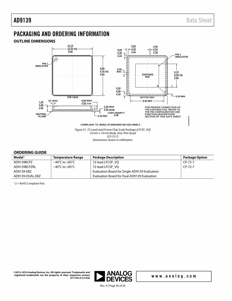
AD9139 Data Sheet
PACKAGING AND ORDERING INFORMATION OUTLINE DIMENSIONS
Figure 51. 72-Lead Lead Frame Chip Scale Package [LFCSP_VQ]
10 mm × 10 mm Body, Very Thin Quad (CP-72-7)
Dimensions shown in millimeters
ORDERING GUIDE Model1 Temperature Range Package Description Package Option AD9139BCPZ −40°C to +85°C 72-lead LFCSP_VQ CP-72-7 AD9139BCPZRL −40°C to +85°C 72-lead LFCSP_VQ CP-72-7 AD9139-EBZ Evaluation Board for Single AD9139 Evaluation AD9139-DUAL-EBZ Evaluation Board for Dual AD9139 Evaluation
1 Z = RoHS Compliant Part.
COMPLIANT TO JEDEC STANDARDS MO-220-VNND-4
0.20 REF
0.80 MAX0.65 TYP
1.000.850.80 0.05 MAX
0.02 NOM
1
18
54
371936
7255
0.500.400.30
8.50 REF
PIN 1INDICATOR
SEATINGPLANE
12° MAX
0.600.420.24
0.600.420.24
0.300.230.18
0.50BSC
PIN 1INDICATOR
COPLANARITY0.08
06-2
5-20
12-A
FOR PROPER CONNECTION OFTHE EXPOSED PAD, REFER TOTHE PIN CONFIGURATION ANDFUNCTION DESCRIPTIONSSECTION OF THIS DATA SHEET.
TOP VIEW
EXPOSEDPAD
BOTTOM VIEW
10.1010.00 SQ9.90
9.859.75 SQ9.65
0.25 MIN
6.156.00 SQ5.85
©2013–2014 Analog Devices, Inc. All rights reserved. Trademarks and registered trademarks are the property of their respective owners. D11744-0-3/14(A)
Rev. A | Page 56 of 56