12-Bit, 300 MSPS High Speed TxDAC+D/A Converter …€¦ · 12-Bit, 300 MSPS High Speed TxDAC+®...
28
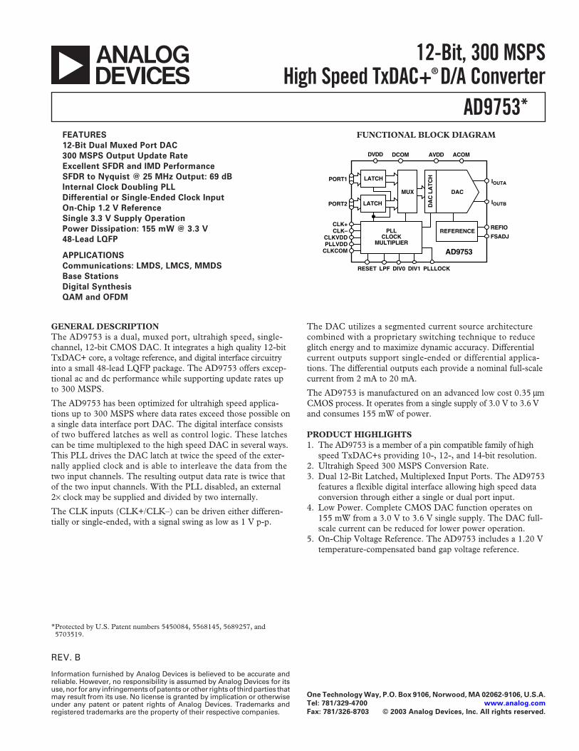
REV. B Information furnished by Analog Devices is believed to be accurate and reliable. However, no responsibility is assumed by Analog Devices for its use, nor for any infringements of patents or other rights of third parties that may result from its use. No license is granted by implication or otherwise under any patent or patent rights of Analog Devices. Trademarks and registered trademarks are the property of their respective companies. One Technology Way, P.O. Box 9106, Norwood, MA 02062-9106, U.S.A. Tel: 781/329-4700 www.analog.com Fax: 781/326-8703 © 2003 Analog Devices, Inc. All rights reserved. AD9753 * 12-Bit, 300 MSPS High Speed TxDAC+ ® D/A Converter *Protected by U.S. Patent numbers 5450084, 5568145, 5689257, and 5703519. FEATURES 12-Bit Dual Muxed Port DAC 300 MSPS Output Update Rate Excellent SFDR and IMD Performance SFDR to Nyquist @ 25 MHz Output: 69 dB Internal Clock Doubling PLL Differential or Single-Ended Clock Input On-Chip 1.2 V Reference Single 3.3 V Supply Operation Power Dissipation: 155 mW @ 3.3 V 48-Lead LQFP APPLICATIONS Communications: LMDS, LMCS, MMDS Base Stations Digital Synthesis QAM and OFDM FUNCTIONAL BLOCK DIAGRAM AVDD ACOM REFIO FSADJ PORT1 I OUTA I OUTB AD9753 DVDD DCOM LATCH LATCH CLK+ CLK– CLKVDD PLLVDD CLKCOM RESET LPF DIV0 DIV1 PLLLOCK PLL CLOCK MULTIPLIER DAC LATCH DAC REFERENCE MUX PORT2 GENERAL DESCRIPTION The AD9753 is a dual, muxed port, ultrahigh speed, single- channel, 12-bit CMOS DAC. It integrates a high quality 12-bit TxDAC+ core, a voltage reference, and digital interface circuitry into a small 48-lead LQFP package. The AD9753 offers excep- tional ac and dc performance while supporting update rates up to 300 MSPS. The AD9753 has been optimized for ultrahigh speed applica- tions up to 300 MSPS where data rates exceed those possible on a single data interface port DAC. The digital interface consists of two buffered latches as well as control logic. These latches can be time multiplexed to the high speed DAC in several ways. This PLL drives the DAC latch at twice the speed of the exter- nally applied clock and is able to interleave the data from the two input channels. The resulting output data rate is twice that of the two input channels. With the PLL disabled, an external 2× clock may be supplied and divided by two internally. The CLK inputs (CLK+/CLK–) can be driven either differen- tially or single-ended, with a signal swing as low as 1 V p-p. The DAC utilizes a segmented current source architecture combined with a proprietary switching technique to reduce glitch energy and to maximize dynamic accuracy. Differential current outputs support single-ended or differential applica- tions. The differential outputs each provide a nominal full-scale current from 2 mA to 20 mA. The AD9753 is manufactured on an advanced low cost 0.35 µ m CMOS process. It operates from a single supply of 3.0 V to 3.6 V and consumes 155 mW of power. PRODUCT HIGHLIGHTS 1. The AD9753 is a member of a pin compatible family of high speed TxDAC+s providing 10-, 12-, and 14-bit resolution. 2. Ultrahigh Speed 300 MSPS Conversion Rate. 3. Dual 12-Bit Latched, Multiplexed Input Ports. The AD9753 features a flexible digital interface allowing high speed data conversion through either a single or dual port input. 4. Low Power. Complete CMOS DAC function operates on 155 mW from a 3.0 V to 3.6 V single supply. The DAC full- scale current can be reduced for lower power operation. 5. On-Chip Voltage Reference. The AD9753 includes a 1.20 V temperature-compensated band gap voltage reference.
Transcript of 12-Bit, 300 MSPS High Speed TxDAC+D/A Converter …€¦ · 12-Bit, 300 MSPS High Speed TxDAC+®...
REV. B
Information furnished by Analog Devices is believed to be accurate andreliable. However, no responsibility is assumed by Analog Devices for itsuse, nor for any infringements of patents or other rights of third parties thatmay result from its use. No license is granted by implication or otherwiseunder any patent or patent rights of Analog Devices. Trademarks andregistered trademarks are the property of their respective companies.
One Technology Way, P.O. Box 9106, Norwood, MA 02062-9106, U.S.A.
Tel: 781/329-4700 www.analog.com
Fax: 781/326-8703 © 2003 Analog Devices, Inc. All rights reserved.
AD9753*
12-Bit, 300 MSPSHigh Speed TxDAC+® D/A Converter
*Protected by U.S. Patent numbers 5450084, 5568145, 5689257, and5703519.
FEATURES
12-Bit Dual Muxed Port DAC
300 MSPS Output Update Rate
Excellent SFDR and IMD Performance
SFDR to Nyquist @ 25 MHz Output: 69 dB
Internal Clock Doubling PLL
Differential or Single-Ended Clock Input
On-Chip 1.2 V Reference
Single 3.3 V Supply Operation
Power Dissipation: 155 mW @ 3.3 V
48-Lead LQFP
APPLICATIONS
Communications: LMDS, LMCS, MMDS
Base Stations
Digital Synthesis
QAM and OFDM
FUNCTIONAL BLOCK DIAGRAM
AVDD ACOM
REFIO
FSADJ
PORT1 IOUTA
IOUTB
AD9753
DVDD DCOM
LATCH
LATCH
CLK+CLK–
CLKVDDPLLVDD
CLKCOM
RESET LPF DIV0 DIV1 PLLLOCK
PLLCLOCK
MULTIPLIER
DA
C L
AT
CH
DAC
REFERENCE
MUX
PORT2
GENERAL DESCRIPTIONThe AD9753 is a dual, muxed port, ultrahigh speed, single-channel, 12-bit CMOS DAC. It integrates a high quality 12-bitTxDAC+ core, a voltage reference, and digital interface circuitryinto a small 48-lead LQFP package. The AD9753 offers excep-tional ac and dc performance while supporting update rates upto 300 MSPS.
The AD9753 has been optimized for ultrahigh speed applica-tions up to 300 MSPS where data rates exceed those possible ona single data interface port DAC. The digital interface consistsof two buffered latches as well as control logic. These latchescan be time multiplexed to the high speed DAC in several ways.This PLL drives the DAC latch at twice the speed of the exter-nally applied clock and is able to interleave the data from thetwo input channels. The resulting output data rate is twice thatof the two input channels. With the PLL disabled, an external2× clock may be supplied and divided by two internally.
The CLK inputs (CLK+/CLK–) can be driven either differen-tially or single-ended, with a signal swing as low as 1 V p-p.
The DAC utilizes a segmented current source architecturecombined with a proprietary switching technique to reduceglitch energy and to maximize dynamic accuracy. Differentialcurrent outputs support single-ended or differential applica-tions. The differential outputs each provide a nominal full-scalecurrent from 2 mA to 20 mA.
The AD9753 is manufactured on an advanced low cost 0.35 µmCMOS process. It operates from a single supply of 3.0 V to 3.6 Vand consumes 155 mW of power.
PRODUCT HIGHLIGHTS1. The AD9753 is a member of a pin compatible family of high
speed TxDAC+s providing 10-, 12-, and 14-bit resolution.2. Ultrahigh Speed 300 MSPS Conversion Rate.3. Dual 12-Bit Latched, Multiplexed Input Ports. The AD9753
features a flexible digital interface allowing high speed dataconversion through either a single or dual port input.
4. Low Power. Complete CMOS DAC function operates on155 mW from a 3.0 V to 3.6 V single supply. The DAC full-scale current can be reduced for lower power operation.
5. On-Chip Voltage Reference. The AD9753 includes a 1.20 Vtemperature-compensated band gap voltage reference.

REV.B–2–
AD9753–SPECIFICATIONS
Parameter Min Typ Max Unit
RESOLUTION 12 Bits
DC ACCURACY1
Integral Linearity Error (INL) –1.5 ±0.5 +1.5 LSBDifferential Nonlinearity (DNL) –1 ±0.4 +1 LSB
ANALOG OUTPUTOffset Error –0.025 ±0.01 +0.025 % of FSRGain Error (Without Internal Reference) –2 ±0.5 +2 % of FSRGain Error (With Internal Reference) –2 ±0.25 +2 % of FSRFull-Scale Output Current2 2.0 20.0 mAOutput Compliance Range –1.0 +1.25 VOutput Resistance 100 kΩOutput Capacitance 5 pF
REFERENCE OUTPUTReference Voltage 1.14 1.20 1.26 VReference Output Current3 100 nA
REFERENCE INPUTInput Compliance Range 0.1 1.25 VReference Input Resistance 1 MΩ
TEMPERATURE COEFFICIENTSOffset Drift 0 ppm of FSR/°CGain Drift (Without Internal Reference) ±50 ppm of FSR/°CGain Drift (With Internal Reference) ±100 ppm of FSR/°CReference Voltage Drift ±50 ppm/°C
POWER SUPPLYSupply Voltages
AVDD 3.0 3.3 3.6 VDVDD 3.0 3.3 3.6 VPLLVDD 3.0 3.3 3.6 VCLKVDD 3.0 3.3 3.6 V
Analog Supply Current (IAVDD)4 33 36 mADigital Supply Current (IDVDD)4 3.5 4.5 mAPLL Supply Current (IPLLVDD)4 4.5 5.1 mAClock Supply Current (ICLKVDD)4 10.0 11.5 mAPower Dissipation4 (3 V, IOUTFS = 20 mA) 155 165 mWPower Dissipation5 (3 V, IOUTFS = 20 mA) 216 mWPower Supply Rejection Ratio6—AVDD –1 +1 % of FSR/VPower Supply Rejection Ratio6—DVDD –0.04 +0.04 % of FSR/V
OPERATING RANGE –40 +85 °CNOTES1Measured at IOUTA, driving a virtual ground.2Nominal full-scale current, IOUTFS, is 32× the IREF current.3An external buffer amplifier is recommended to drive any external load.4100 MSPS fDAC with PLL on, fOUT = 1 MHz, all supplies = 3.0 V.5300 MSPS fDAC.6± 5% power supply variation.
Specifications subject to change without notice.
DC SPECIFICATIONS (TMIN to TMAX, AVDD = 3.3 V, DVDD = 3.3 V, PLLVDD = 3.3 V, CLKVDD = 3.3 V, IOUTFS = 20 mA, unlessotherwise noted.)

REV. B
AD9753
–3–
Parameter Min Typ Max Unit
DYNAMIC PERFORMANCEMaximum Output Update Rate (fDAC) 300 MSPSOutput Settling Time (tST) (to 0.1%)1 11 nsOutput Propagation Delay (tPD)1 1 nsGlitch Impulse1 5 pV-sOutput Rise Time (10% to 90%)1 2.5 nsOutput Fall Time (10% to 90%)1 2.5 nsOutput Noise (IOUTFS = 20 mA) 50 pA/√HzOutput Noise (IOUTFS = 2 mA) 30 pA/√Hz
AC LINEARITYSpurious-Free Dynamic Range to Nyquist
fDAC = 100 MSPS; fOUT = 1.00 MHz 0 dBFS Output 72 82 dBc –6 dBFS Output 76 dBc –12 dBFS Output 76 dBcfDATA = 65 MSPS; fOUT = 1.1 MHz2 77 dBcfDATA = 65 MSPS; fOUT = 5.1 MHz2 77 dBcfDATA = 65 MSPS; fOUT = 10.1 MHz2 76 dBcfDATA = 65 MSPS; fOUT = 20.1 MHz2 72 dBcfDATA = 65 MSPS; fOUT = 30.1 MHz2 68 dBcfDAC = 200 MSPS; fOUT = 1.1 MHz 78 dBcfDAC = 200 MSPS; fOUT = 11.1 MHz 75 dBcfDAC = 200 MSPS; fOUT = 31.1 MHz 70 dBcfDAC = 200 MSPS; fOUT = 51.1 MHz 70 dBcfDAC = 200 MSPS; fOUT = 71.1 MHz 67 dBcfDAC = 300 MSPS; fOUT = 1.1 MHz 78 dBcfDAC = 300 MSPS; fOUT = 26.1 MHz 69 dBcfDAC = 300 MSPS; fOUT = 51.1 MHz 65 dBcfDAC = 300 MSPS; fOUT = 101.1 MHz 59 dBcfDAC = 300 MSPS; fOUT = 141.1 MHz 58 dBc
Spurious-Free Dynamic Range within a WindowfDAC = 100 MSPS; fOUT = 1 MHz; 2 MHz Span 0 dBFS Output 82.5 92 dBcfDAC = 65 MSPS; fOUT = 5.02 MHz; 2 MHz Span 85 dBcfDAC = 150 MSPS; fOUT = 5.04 MHz; 4 MHz Span 85 dBc
Total Harmonic DistortionfDAC = 100 MSPS; fOUT = 1.00 MHz 0 dBFS –82 –71 dBcfDAC = 65 MHz; fOUT = 2.00 MHz –76 dBcfDAC = 160 MHz; fOUT = 2.00 MHz –76 dBc
Multitone Power Ratio (Eight Tones at 110 kHz Spacing)fDAC = 65 MSPS; fOUT = 2.00 MHz to 2.77 MHz 0 dBFS Output 73 dBc –6 dBFS Output 71 dBc –12 dBFS Output 69 dBc
NOTES1Measured single-ended into 50 Ω load.2Single-Port Mode (PLL disabled, DIV0 = 1, DIV1 = 0, data on Port 1).
Specifications subject to change without notice.
DYNAMIC SPECIFICATIONS (TMIN to TMAX, AVDD = 3.3 V, DVDD = 3.3 V, PLLVDD = 0 V, CLKVDD = 3.3 V, IOUTFS = 20 mA,Differential Transformer-Coupled Output, 50 V Doubly Terminated, unless otherwise noted.)
REV. B–4–
AD9753
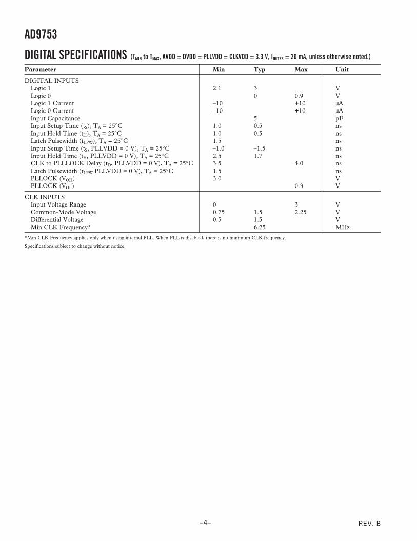
DIGITAL SPECIFICATIONS (TMIN to TMAX, AVDD = DVDD = PLLVDD = CLKVDD = 3.3 V, IOUTFS = 20 mA, unless otherwise noted.)
Parameter Min Typ Max Unit
DIGITAL INPUTSLogic 1 2.1 3 VLogic 0 0 0.9 VLogic 1 Current –10 +10 µALogic 0 Current –10 +10 µAInput Capacitance 5 pFInput Setup Time (tS), TA = 25°C 1.0 0.5 nsInput Hold Time (tH), TA = 25°C 1.0 0.5 nsLatch Pulsewidth (tLPW), TA = 25°C 1.5 nsInput Setup Time (tS, PLLVDD = 0 V), TA = 25°C –1.0 –1.5 nsInput Hold Time (tH, PLLVDD = 0 V), TA = 25°C 2.5 1.7 nsCLK to PLLLOCK Delay (tD, PLLVDD = 0 V), TA = 25°C 3.5 4.0 nsLatch Pulsewidth (tLPW PLLVDD = 0 V), TA = 25°C 1.5 nsPLLOCK (VOH) 3.0 VPLLOCK (VOL) 0.3 V
CLK INPUTSInput Voltage Range 0 3 VCommon-Mode Voltage 0.75 1.5 2.25 VDifferential Voltage 0.5 1.5 VMin CLK Frequency* 6.25 MHz
*Min CLK Frequency applies only when using internal PLL. When PLL is disabled, there is no minimum CLK frequency.
Specifications subject to change without notice.
REV. B
AD9753
–5–
CAUTIONESD (electrostatic discharge) sensitive device. Electrostatic charges as high as 4000 V readilyaccumulate on the human body and test equipment and can discharge without detection. Although theAD9753 features proprietary ESD protection circuitry, permanent damage may occur on devicessubjected to high energy electrostatic discharges. Therefore, proper ESD precautions are recommendedto avoid performance degradation or loss of functionality.
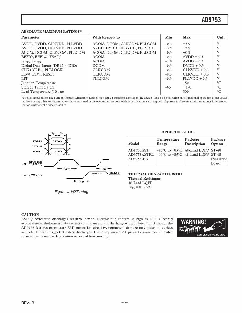
PORT 1 DATA X
DATA Y
tHtS
tLPW tPD
DATA X DATA Y
tPD
PORT 2
IOUTA OR IOUTB
INPUT CLK(PLL ENABLED)
DATA IN
Figure 1. I/O Timing
ORDERING GUIDE
Temperature Package PackageModel Range Description Option
AD9753AST –40°C to +85°C 48-Lead LQFP ST-48AD9753ASTRL –40°C to +85°C 48-Lead LQFP ST-48AD9753-EB Evaluation
Board
THERMAL CHARACTERISTICThermal Resistance48-Lead LQFP JA = 91°C/W
ABSOLUTE MAXIMUM RATINGS*
Parameter With Respect to Min Max Unit
AVDD, DVDD, CLKVDD, PLLVDD ACOM, DCOM, CLKCOM, PLLCOM –0.3 +3.9 VAVDD, DVDD, CLKVDD, PLLVDD AVDD, DVDD, CLKVDD, PLLVDD –3.9 +3.9 VACOM, DCOM, CLKCOM, PLLCOM ACOM, DCOM, CLKCOM, PLLCOM –0.3 +0.3 VREFIO, REFLO, FSADJ ACOM –0.3 AVDD + 0.3 VIOUTA, IOUTB ACOM –1.0 AVDD + 0.3 VDigital Data Inputs (DB13 to DB0) DCOM –0.3 DVDD + 0.3 VCLK+/CLK–, PLLLOCK CLKCOM –0.3 CLKVDD + 0.3 VDIV0, DIV1, RESET CLKCOM –0.3 CLKVDD + 0.3 VLPF PLLCOM –0.3 PLLVDD + 0.3 VJunction Temperature 150 °CStorage Temperature –65 +150 °CLead Temperature (10 sec) 300 °C*Stresses above those listed under Absolute Maximum Ratings may cause permanent damage to the device. This is a stress rating only; functional operation of the deviceat these or any other conditions above those indicated in the operational sections of this specification is not implied. Exposure to absolute maximum ratings for extendedperiods may affect device reliability.
REV. B–6–
AD9753
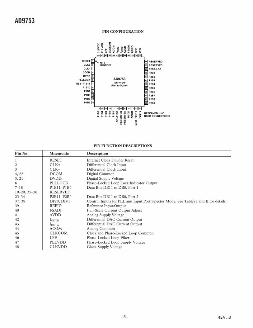
PIN FUNCTION DESCRIPTIONS
Pin No. Mnemonic Description
1 RESET Internal Clock Divider Reset2 CLK+ Differential Clock Input3 CLK– Differential Clock Input4, 22 DCOM Digital Common5, 21 DVDD Digital Supply Voltage6 PLLLOCK Phase-Locked Loop Lock Indicator Output7–18 P1B11–P1B0 Data Bits DB11 to DB0, Port 119–20, 35–36 RESERVED23–34 P2B11–P2B0 Data Bits DB11 to DB0, Port 237, 38 DIV0, DIV1 Control Inputs for PLL and Input Port Selector Mode. See Tables I and II for details.39 REFIO Reference Input/Output40 FSADJ Full-Scale Current Output Adjust41 AVDD Analog Supply Voltage42 IOUTB Differential DAC Current Output43 IOUTA Differential DAC Current Output44 ACOM Analog Common45 CLKCOM Clock and Phase-Locked Loop Common46 LPF Phase-Locked Loop Filter47 PLLVDD Phase-Locked Loop Supply Voltage48 CLKVDD Clock Supply Voltage
PIN CONFIGURATION
13 14 15 16 17 18 19 20 21 22 23 24
1
2
3
4
5
6
7
8
9
10
11
12
48 47 46 45 44 39 38 3743 42 41 40
PIN 1IDENTIFIER
TOP VIEW(Not to Scale)
36
35
34
33
32
31
30
29
28
27
26
25
AD9753
RESERVED
RESERVED
P2B0–LSB
P2B1
P2B2
P2B3
P2B4
P2B5
P2B6
P2B7
P2B8
P2B9
RESET
CLK+
CLK–
DCOM
DVDD
PLLLOCK
MSB–P1B11
P1B10
P1B9
P1B8
P1B7
P1B6
CL
KV
DD
PL
LV
DD
LP
F
CL
KC
OM
AC
OM
I OU
TA
I OU
TB
AV
DD
FS
AD
J
RE
FIO
DIV
1
DIV
0
P1B
5
P1B
4
P1B
3
P1B
2
P1B
1
LS
B–P
1B0
RE
SE
RV
ED
RE
SE
RV
ED
DV
DD
DC
OM
MS
B–P
2B11
P2B
10 RESERVED = NOUSER CONNECTIONS

REV. B
AD9753
–7–
TERMINOLOGYLinearity Error (Also Called Integral Nonlinearity or INL)Linearity error is defined as the maximum deviation of the actualanalog output from the ideal output, determined by a straightline drawn from zero to full scale.
Differential Nonlinearity (DNL)DNL is the measure of the variation in analog value, normalizedto full scale, associated with a 1 LSB change in digital input code.
MonotonicityA D/A converter is monotonic if the output either increases orremains constant as the digital input increases.
Offset ErrorThe deviation of the output current from the ideal of zero iscalled offset error. For IOUTA, 0 mA output is expected when theinputs are all 0s. For IOUTB, 0 mA output is expected when allinputs are set to 1s.
Gain ErrorThe difference between the actual and ideal output span. Theactual span is determined by the output when all inputs are setto 1s, minus the output when all inputs are set to 0s.
Output Compliance RangeThe range of allowable voltage at the output of a current-outputDAC. Operation beyond the maximum compliance limits maycause either output stage saturation or breakdown, resulting innonlinear performance.
Temperature DriftSpecified as the maximum change from the ambient (25°C)value to the value at either TMIN or TMAX. For offset and gaindrift, the drift is reported in ppm of full-scale range (FSR) perdegree Celsius. For reference drift, the drift is reported in ppmper degree Celsius.
Power Supply RejectionThe maximum change in the full-scale output as the suppliesare varied from minimum to maximum specified voltages.
Settling TimeThe time required for the output to reach and remain within aspecified error band about its final value, measured from thestart of the output transition.
Glitch ImpulseAsymmetrical switching times in a DAC give rise to undesiredoutput transients that are quantified by a glitch impulse. It isspecified as the net area of the glitch in pV-s.
Spurious-Free Dynamic RangeThe difference, in dB, between the rms amplitude of the outputsignal and the peak spurious signal over the specified bandwidth.
Total Harmonic Distortion (THD)THD is the ratio of the rms sum of the first six harmonic com-ponents to the rms value of the measured fundamental. It isexpressed as a percentage or in decibels (dB).
Signal-to-Noise Ratio (SNR)SNR is the ratio of the rms value of the measured output signalto the rms sum of all other spectral components below the Nyquistfrequency, excluding the first six harmonics and dc. The valuefor SNR is expressed in decibels.
Adjacent Channel Power Ratio (ACPR)A ratio in dBc between the measured power within a channelrelative to its adjacent channel.
AD9753
IOUTA
IOUTB
SEGMENTEDSWITCHES FOR
DB0 TO DB11DAC
FSADJ
REFIO
1.2V REF
CLK+ PLLLOCK
DIGITAL DATA INPUTS
0.1FRSET2k
1k
50
MINICIRCUITS
T1-1T
TO ROHDE &SCHWARZFSEA30SPECTRUMANALYZER
DB0 – DB11
TEKTRONIX DG2020OR
AWG2021 w/OPTION 4
LECROY 9210PULSE GENERATOR
(FOR DATA RETIMING)
DCOM
PMOS CURRENTSOURCE ARRAY
AVDD
3.0V TO 3.6V
DVDD
2 –1 MUX
PORT 1 LATCH
DAC LATCH
ACOMPORT 2 LATCH
CLK–
PLLCIRCUITRY
PLLVDDCLKVDDRESETLPFCLKCOMDIV0DIV1
50
DB0 – DB11
MINICIRCUITS
T1-1T
1k3.0V TO 3.6V
HP8644SIGNALGENERATOR
PLL ENABLEDPLL DISABLED
Figure 2. Basic AC Characterization Test Setup

REV. B–8–
AD9753–Typical Performance Characteristics
fOUT (MHz)
90
70
403550
SF
DR
(d
Bc)
80
60
50
10 15 20 25 30
0dBmFS
–6dBmFS
–12dBmFS
TPC 1. Single-Tone SFDR vs. fOUT @fDAC = 65 MSPS, Single-Port Mode
fOUT (MHz)
90
70
401000
SF
DR
(d
Bc)
80
60
50
20 40 60 80 120 140
200MSPS
300MSPS
65MSPS
TPC 4. SFDR vs. fOUT @ 0 dBFS
AOUT (dB)
90
70
40–6–16
SF
DR
(d
Bc)
80
60
50
–14 –12 –10 –8 –4 –2 0
11.82MHz @ 130MSPS
18.18MHz @ 200MSPS
27.27MHz @ 300MSPS
TPC 7. Single-Tone SFDR vs.AOUT @ fOUT = fDAC/11
fOUT (MHz)
90
70
40100100
SF
DR
(d
Bc)
80
60
50
20 30 40 50 60 70 80 90
0dBmFS–6dBmFS
–12dBmFS
TPC 2. Single-Tone SFDR vs.fOUT @ fDAC = 200 MSPS
fOUT (MHz)
90
70
40100100
SF
DR
(d
Bc)
80
60
50
20 30 40 50 60 70 80 90
SFDR NEAR CARRIERS(2F1-F2, 2F2-F1)
SFDR OVERNYQUIST BAND
TPC 5. Two-Tone IMD vs. fOUT @fDAC = 200 MSPS, 1 MHz Spacingbetween Tones, 0 dBFS
AOUT (dBm)
90
70
40–6–16
SF
DR
(d
Bc)
80
60
50
–14 –12 –10 –8 –4 –2 0
26MHz @ 130MSPS
40MHz @ 200MSPS
60MHz @ 300MSPS
TPC 8. Single-Tone SFDR vs.AOUT @ fOUT = fDAC/5
fOUT (MHz)
90
70
401000
SF
DR
(d
Bc)
80
60
50
20 40 60 80 120 140 160
0dBmFS
–6dBmFS
–12dBmFS
TPC 3. Single-Tone SFDR vs.fOUT @ fDAC = 300 MSPS
fOUT (MHz)
90
70
401000
SF
DR
(d
Bc)
80
60
50
20 40 60 80 120 140 160
SFDR CLOSE TO CARRIERS(2F1-F2, 2F2-F1)
SFDR OVER NYQUIST BAND
TPC 6. Two-Tone IMD vs. fOUT @fDAC = 300 MSPS, 1 MHz Spacingbetween Tones, 0 dBFS
AOUT (dBm)
90
70
40–6–16
SF
DR
(d
Bc)
80
60
50
–14 –12 –10 –8 –4 –2 0–18–20
18.18MHz/19.18MHz@ 200MSPS
11.82MHz/12.82MHz@ 130MSPS
27.27MHz/28.27MHz@ 300MSPS
TPC 9. Two-Tone IMD (Third OrderProducts) vs. AOUT @ fOUT = fDAC/11
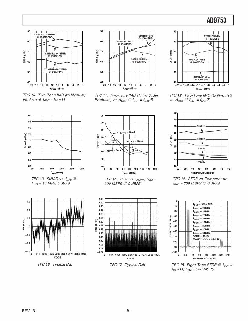
REV. B
AD9753
–9–
AOUT (dBm)
90
70
40–6–16
SF
DR
(d
Bc)
80
60
50
–14 –12 –10 –8 –4 –2 0–18–20
18.18MHz/19.18MHz@ 200MSPS
11.82MHz/12.82MHz@ 130MSPS
27.27MHz/28.27MHz@ 300MSPS
TPC 10. Two-Tone IMD (to Nyquist)vs. AOUT @ fOUT = fDAC/11
fDAC (MHz)
90
70
85
30050
SIN
AD
(d
Bm
)
80
60
50100 150 200 250
75
65
55
TPC 13. SINAD vs. fDAC @fOUT = 10 MHz, 0 dBFS
CODE
0
–0.4
40955110
INL
(L
SB
) 0.2
–0.2
1023 1535 2047 3071–0.6
3583
0.6
2559
0.1
0.4
TPC 16. Typical INL
AOUT (dBm)
90
70
40–6–16
SF
DR
(d
Bc)
80
60
50
–14 –12 –10 –8 –4 –2 0–18–20
60MHz/61MHz@ 300MSPS
26MHz/27MHz@ 130MSPS
40MHz/41MHz@ 200MSPS
TPC 11. Two-Tone IMD (Third OrderProducts) vs. AOUT @ fOUT = fDAC/5
fOUT (MHz)
75
65
50
160200
SF
DR
(d
Bc)
70
60
55
40 60 80 100 120
45
40140
IOUTFS = 20mA
IOUTFS = 10mA
IOUTFS = 5mA
TPC 14. SFDR vs. IOUTFS, fDAC =300 MSPS @ 0 dBFS
CODE40955110
DN
L (
LS
B)
0.50
1023 1535 2047 3071–0.02
3583
0.54
2559
0.46
0.42
0.38
0.34
0.30
0.26
0.22
0.18
0.14
0.10
0.06
0.02
TPC 17. Typical DNL
AOUT (dBm)
90
70
40–6–16
SF
DR
(d
Bc)
80
60
50
–14 –12 –10 –8 –4 –2 0–18–20
60MHz/61MHz@ 300MSPS
26MHz/27MHz@ 130MSPS
40MHz/41MHz@ 200MSPS
TPC 12. Two-Tone IMD (to Nyquist)vs. AOUT @ fOUT = fDAC/5
TEMPERATURE (C)
75
65
50
90–30–50S
FD
R (
dB
c)
70
60
55
–10 10 30 50
45
4070
80
10MHz
40MHz
120MHz
80MHz
TPC 15. SFDR vs. Temperature,fDAC = 300 MSPS @ 0 dBFS
FREQUENCY (MHz)
–10
–30
–80
200
AM
PL
ITU
DE
(d
Bm
)
–20
–40
–75
40 60 100 120
–95
–100140
0
–50
–60
80
fDAC = 300MSPSfOUT1 = 24MHzfOUT2 = 25MHzfOUT3 = 26MHzfOUT4 = 27MHzfOUT5 = 28MHzfOUT6 = 29MHzfOUT7 = 30MHzfOUT8 = 31MHzSFDR = 58dBcMAGNITUDE = 0dBFS
0
TPC 18. Eight-Tone SFDR @ fOUT ≈fDAC/11, fDAC = 300 MSPS

REV. B–10–
AD9753
AD9753
IOUTA
IOUTB
SEGMENTEDSWITCHES FOR
DB0 TO DB11DAC
FSADJ
REFIO
1.2V REF
DIV0 PLLLOCKDIGITAL DATA INPUTS
0.1FRSET2k
RLOAD50
DB0 – DB11
DCOM
PMOS CURRENTSOURCE ARRAY
AVDD
3.0V TO 3.6V
DVDD
2 –1 MUX
PORT 1 LATCH
DAC LATCH
ACOMPORT 2 LATCH
DIV1
PLLCIRCUITRY
PLLVDDCLKVDDCLK+CLK–CLKCOMRESETLPF
DB0 – DB11
VOUTB RLOAD50
VOUTA
VDIFF = VOUTA – VOUTB
Figure 3. Simplified Block Diagram
FUNCTIONAL DESCRIPTIONFigure 3 shows a simplified block diagram of the AD9753. TheAD9753 consists of a PMOS current source array capable ofproviding up to 20 mA of full-scale current, IOUTFS. Thearray is divided into 31 equal sources that make up the fivemost significant bits (MSBs). The next four bits, or middle bits,consist of 15 equal current sources whose value is 1/16th of anMSB current source. The remaining LSBs are a binary weightedfraction of the middle bit current sources. Implementing themiddle and lower bits with current sources, instead of an R-2Rladder, enhances dynamic performance for multitone or lowamplitude signals and helps maintain the DAC’s high outputimpedance (i.e., >100 kΩ).
All of the current sources are switched to one of the twooutputs (i.e., IOUTA or IOUTB) via PMOS differential currentswitches. The switches are based on a new architecture thatdrastically improves distortion performance. This new switcharchitecture reduces various timing errors and provides matchingcomplementary drive signals to the inputs of the differentialcurrent switches.
The analog and digital sections of the AD9753 have separatepower supply inputs (i.e., AVDD and DVDD) that can operateindependently over a 3.0 V to 3.6 V range. The digital section,which is capable of operating at a 300 MSPS clock rate, consistsof edge-triggered latches and segment decoding logic circuitry.The analog section includes the PMOS current sources, theassociated differential switches, a 1.20 V band gap voltage refer-ence, and a reference control amplifier.
The full-scale output current is regulated by the reference controlamplifier and can be set from 2 mA to 20 mA via an externalresistor, RSET. The external resistor, in combination with boththe reference control amplifier and voltage reference VREFIO, setsthe reference current IREF, which is replicated to the segmentedcurrent sources with the proper scaling factor. The full-scalecurrent, IOUTFS, is 32 times the value of IREF.
REFERENCE OPERATIONThe AD9753 contains an internal 1.20 V band gap reference.This can easily be overdriven by an external reference with noeffect on performance. REFIO serves as either an input or output,depending on whether the internal or an external reference isused. To use the internal reference, simply decouple the REFIOpin to ACOM with a 0.1 µF capacitor. The internal referencevoltage will be present at REFIO. If the voltage at REFIO is tobe used elsewhere in the circuit, an external buffer amplifierwith an input bias current less than 100 nA should be used. Anexample of the use of the internal reference is given in Figure 4.
A low impedance external reference can be applied to REFIO,as shown in Figure 5. The external reference may provide eithera fixed reference voltage to enhance accuracy and drift perfor-mance or a varying reference voltage for gain control. Notethat the 0.1 µF compensation capacitor is not required sincethe internal reference is overdriven, and the relatively high inputimpedance of REFIO minimizes any loading of the externalreference.
1.2V REF
AVDD
IREF
CURRENTSOURCEARRAY
REFIO
FSADJ
2k
0.1F
AD9753REFERENCE
SECTION
ADDITIONALEXTERNAL
LOAD
OPTIONALEXTERNAL
REFERENCEBUFFER
Figure 4. Internal Reference Configuration
1.2V REF
AVDD
IREF
CURRENTSOURCEARRAY
REFIO
FSADJ
2k
AD9753REFERENCE
SECTION
EXTERNALREFERENCE
AVDD
Figure 5. External Reference Configuration

REV. B
AD9753
–11–
PORT 1 DATA X
DATA Y
tHtS
tLPW tPD
DATA X DATA Y
1/2 CYCLE + tPD
PORT 2
IOUTA OR IOUTB
CLK
DATA IN
Figure 7a. DAC Input Timing Requirements withPLL Active, Single Clock Cycle
PORT 1
DATA X DATA Z
DATA X
DATA Y
PORT 2
IOUTA OR IOUTB
CLK
DATA IN
DATA Z
DATA WXXX
DATA W DATA Y
Figure 7b. DAC Input Timing Requirements withPLL Active, Multiple Clock Cycles
Typically, the VCO can generate outputs of 100 MHz to400 MHz. The range control is used to keep the VCO operatingwithin its designed range, while allowing input clocks as low as6.25 MHz. With the PLL active, logic levels at DIV0 and DIV1determine the divide (prescaler) ratio of the range controller.Table I gives the frequency range of the input clock for thedifferent states of DIV0 and DIV1.
Table I. CLK Rates for DIV0, DIV1 Levels with PLL Active
CLK Frequency DIV1 DIV0 Range Controller
50 MHz–150 MHz 0 0 ÷125 MHz–100 MHz 0 1 ÷212.5 MHz–50 MHz 1 0 ÷46.25 MHz–25 MHz 1 1 ÷8
A 392 Ω resistor and 1.0 µF capacitor connected in series fromLPF to PLLVDD are required to optimize the phase noise versusthe settling/acquisition time characteristics of the PLL. Toobtain optimum noise and distortion performance, PLLVDDshould be set to a voltage level similar to DVDD andCLKVDD.
In general, the best phase noise performance for any PLL rangecontrol setting is achieved with the VCO operating near its maxi-mum output frequency of 400 MHz.
As stated earlier, applications requiring input data rates below6.25 MSPS must disable the PLL clock multiplier and providean external 2× reference clock. At higher data rates however,applications already containing a low phase noise (i.e., jitter)
REFERENCE CONTROL AMPLIFIERThe AD9753 also contains an internal control amplifier that isused to regulate the DAC’s full-scale output current, IOUTFS.The control amplifier is configured as a voltage-to-currentconverter as shown in Figure 4, so that its current output, IREF, isdetermined by the ratio of VREFIO and an external resistor, RSET,as stated in Equation 4. IREF is applied to the segmented currentsources with the proper scaling factor to set IOUTFS, as stated inEquation 3.
The control amplifier allows a wide (10:1) adjustment span ofIOUTFS over a 2 mA to 20 mA range by setting IREF between62.5 µA and 625 µA. The wide adjustment span of IOUTFS
provides several application benefits. The first benefit relatesdirectly to the power dissipation of the AD9753, which isproportional to IOUTFS (refer to the Power Dissipation section).The second benefit relates to the 20 dB adjustment, which isuseful for system gain control purposes.
The small signal bandwidth of the reference control amplifier isapproximately 500 kHz and can be used for low frequency,small signal multiplying applications.
PLL CLOCK MULTIPLIER OPERATIONThe Phase-Locked Loop (PLL) is intrinsic to the operation ofthe AD9753 in that it produces the necessary internally syn-chronized 2× clock for the edge-triggered latches, multiplexer,and DAC.
With PLLVDD connected to its supply voltage, the AD9753 isin PLL mode. Figure 6 shows a functional block diagram of theAD9753 clock control circuitry with PLL active. The circuitryconsists of a phase detector, charge pump, voltage controlledoscillator (VCO), input data rate range control, clock logiccircuitry, and control input/outputs. The ÷2 logic in the feed-back loop allows the PLL to generate the 2× clock needed forthe DAC output latch.
CLKCOM
TO INPUTLATCHES
CLKVDD(3.0V TO 3.6V) PLLLOCK
CHARGEPUMP
PHASEDETECTOR
LPF PLLVDD
VCO
392 1.0F3.0V TO3.6V
RANGECONTROL(1, 2, 4, 8)
DIV0
DIV1
DIFFERENTIAL- TO-
SINGLE-ENDEDAMP
2
TO DACLATCH
CLK+
CLK–
AD9753
Figure 6. Clock Circuitry with PLL Active
Figure 7 defines the input and output timing for the AD9753with the PLL active. CLK in Figure 7 represents the clockthat is generated external to the AD9753. The input data atboth Ports 1 and 2 is latched on the same CLK rising edge.CLK may be applied as a single-ended signal by tying CLK– tomidsupply and applying CLK to CLK+, or as a differentialsignal applied to CLK+ and CLK–.
RESET has no purpose when using the internal PLL and shouldbe grounded. When the AD9753 is in PLL mode, PLLLOCKis the output of the internal phase detector. When locked, thelock output in this mode will be a Logic 1.

REV. B–12–
AD9753reference clock that is twice the input data rate should considerdisabling the PLL clock multiplier to achieve the best SNRperformance from the AD9753. Note, the SFDR performanceof the AD9753 remains unaffected with or without the PLLclock multiplier enabled.
The effects of phase noise on the AD9753’s SNR performancebecome more noticeable at higher reconstructed output frequen-cies and signal levels. Figure 8 compares the phase noise of afull-scale sine wave at exactly fDATA/4 at different data rates(thus carrier frequency) with the optimum DIV1, DIV0 setting.
SNR is partly a function of the jitter generated by the clockcircuitry. As a result, any noise on PLLVDD or CLKVDD maydecrease the SNR at the output of the DAC. To minimize thispotential problem, PLLVDD and CLKVDD can be connectedto DVDD using an LC filter network similar to the one shownin Figure 9.
FREQUENCY OFFSET (MHz)
0
–20
–110510
NO
ISE
DE
NS
ITY
(d
Bm
/Hz)
–10
–30
–40
–50
–60
–70
–80
–90
–100
2 3 4
PLL ON, fDATA = 150MSPS
PLL OFF, fDATA = 50MSPS
Figure 8. Phase Noise of PLL Clock Multiplier atfOUT = fDATA/4 at Different fDATA Settings with DIV0/DIV1Optimized, Using R&S FSEA30 Spectrum Analyzer
100FELECT.
10FTANT.
0.1FCER.TTL/CMOS
LOGICCIRCUITS
3.3V POWER SUPPLY
FERRITEBEADS
CLKVDD
PLLVDD
CLKCOM
Figure 9. LC Network for Power Filtering
DAC TIMING WITH PLL ACTIVEAs described in Figure 7, in PLL active mode, Port 1 andPort 2 input latches are updated on the rising edge of CLK. Onthe same rising edge, data previously present in the input Port 2latch is written to the DAC output latch. The DAC output willupdate after a short propagation delay (tPD).
Following the rising edge of CLK at a time equal to half of itsperiod, the data in the Port 1 latch will be written to the DACoutput latch, again with a corresponding change in the DACoutput. Due to the internal PLL, the time at which the data inthe Port 1 and Port 2 input latches is written to the DAC latchis independent of the duty cycle of CLK. When using the PLL,the external clock can be operated at any duty cycle that meetsthe specified input pulsewidth.
On the next rising edge of CLK, the cycle begins again with thetwo input port latches being updated, and the DAC output latchbeing updated with the current data in the Port 2 input latch.
PLL DISABLED MODEWhen PLLVDD is grounded, the PLL is disabled. An externalclock must now drive the CLK inputs at the desired DAC out-put update rate. The speed and timing of the data present atinput Ports 1 and 2 are now dependent on whether or not theAD9753 is interleaving the digital input data or only respondingto data on a single port. Figure 10 is a functional block diagramof the AD9753 clock control circuitry with the PLL disabled.
PLLVDD
TO DACLATCH
PLLLOCK
CLOCKLOGIC
(1 OR 2)DIFFERENTIAL-
TO-SINGLE-ENDED
AMP
TOINTERNALMUX
CLKIN+
CLKIN–
AD9753
RESET DIV0 DIV1
TO INPUTLATCHES
Figure 10. Clock Circuitry with PLL Disabled
DIV0 and DIV1 no longer control the PLL but are used to setthe control on the input mux for either interleaving or non-interleaving the input data. The different modes for states ofDIV0 and DIV1 are given in Table II.
Table II. Input Mode for DIV0,DIV1 Levels with PLL Disabled
Input Mode DIV1 DIV0
Interleaved (2×) 0 0NoninterleavedPort 1 Selected 0 1Port 2 Selected 1 0Not Allowed 1 1
REV. B
AD9753
–13–
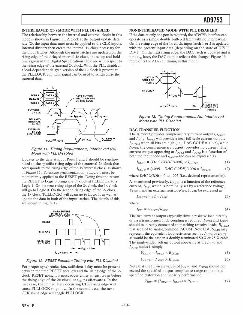
INTERLEAVED (2) MODE WITH PLL DISABLEDThe relationship between the internal and external clocks in thismode is shown in Figure 11. A clock at the output update datarate (2× the input data rate) must be applied to the CLK inputs.Internal dividers then create the internal 1× clock necessary forthe input latches. Although the input latches are updated on therising edge of the delayed internal 1× clock, the setup-and-holdtimes given in the Digital Specifications table are with respect tothe rising edge of the external 2× clock. With the PLL disabled,a load-dependent delayed version of the 1× clock is present atthe PLLLOCK pin. This signal can be used to synchronize theexternal data.
PORT 1 DATA X
DATA Y
tHtS
tLPW
tPD
DATA X DATA Y
PORT 2
IOUTA OR IOUTB
DELAYEDINTERNAL
1 CLK
DATA IN
tPD
tD
DATA ENTERSINPUT LATCHESON THIS EDGE
EXTERNAL2 CLK
EXTERNAL1 CLK
@ PLLLOCK
Figure 11. Timing Requirements, Interleaved (2×)Mode with PLL Disabled
Updates to the data at input Ports 1 and 2 should be synchro-nized to the specific rising edge of the external 2× clock thatcorresponds to the rising edge of the 1× internal clock, as shownin Figure 11. To ensure synchronization, a Logic 1 must bemomentarily applied to the RESET pin. Doing this and return-ing RESET to Logic 0 brings the 1× clock at PLLLOCK to aLogic 1. On the next rising edge of the 2× clock, the 1× clockwill go to Logic 0. On the second rising edge of the 2× clock,the 1× clock (PLLLOCK) will again go to Logic 1, as well asupdate the data in both of the input latches. The details of thisare shown in Figure 12.
RESET
PLLLOCK
EXTERNAL2 CLOCK
tRH = 1.2ns
tRS = 0.2ns
DATA ENTERSINPUT LATCHES
ON THESE EDGES
Figure 12. RESET Function Timing with PLL Disabled
For proper synchronization, sufficient delay must be presentbetween the time RESET goes low and the rising edge of the 2×clock. RESET going low must occur either at least tRS ns beforethe rising edge of the 2× clock, or tRH ns afterwards. In thefirst case, the immediately occurring CLK rising edge willcause PLLLOCK to go low. In the second case, the nextCLK rising edge will toggle PLLLOCK.
NONINTERLEAVED MODE WITH PLL DISABLEDIf the data at only one port is required, the AD9753 interface canoperate as a simple double buffered latch with no interleaving.On the rising edge of the 1× clock, input latch 1 or 2 is updatedwith the present input data (depending on the state of DIV0/DIV1). On the next rising edge, the DAC latch is updated and atime tPD later, the DAC output reflects this change. Figure 13represents the AD9753 timing in this mode.
tHtS
tLPW tPD
DATA OUTPORT 1 OR
PORT 2
1 CLOCK
IOUTA OR IOUTB XX
DATA INPORT 1 OR
PORT 2
Figure 13. Timing Requirements, NoninterleavedMode with PLL Disabled
DAC TRANSFER FUNCTIONThe AD9753 provides complementary current outputs, IOUTAand IOUTB. IOUTA will provide a near full-scale current output,IOUTFS, when all bits are high (i.e., DAC CODE = 4095), whileIOUTB, the complementary output, provides no current. Thecurrent output appearing at IOUTA and IOUTB is a function ofboth the input code and IOUTFS and can be expressed as
IOUTA = (DAC CODE/4096) × IOUTFS (1)
IOUTB = (4095 – DAC CODE)/4096 × IOUTFS (2)
where DAC CODE = 0 to 4095 (i.e., decimal representation).
As mentioned previously, IOUTFS is a function of the referencecurrent, IREF, which is nominally set by a reference voltage,VREFIO, and an external resistor RSET. It can be expressed as
IOUTFS = 32 × IREF (3)
where
IREF = VREFIO/RSET (4)
The two current outputs typically drive a resistive load directlyor via a transformer. If dc coupling is required, IOUTA and IOUTB
should be directly connected to matching resistive loads, RLOAD,that are tied to analog common, ACOM. Note that RLOAD mayrepresent the equivalent load resistance seen by IOUTA or IOUTB
as would be the case in a doubly terminated 50 Ω or 75 Ω cable.The single-ended voltage output appearing at the IOUTA andIOUTB nodes is simply
VOUTA = IOUTA × RLOAD (5)
VOUTB = IOUTB × RLOAD (6)
Note that the full-scale values of VOUTA and VOUTB should notexceed the specified output compliance range to maintainspecified distortion and linearity performance.
VDIFF = (IOUTA – IOUTB) × RLOAD (7)
REV. B–14–
AD9753Substituting the values of IOUTA, IOUTB, and IREF, VDIFF can beexpressed as
VDIFF = (2 DAC CODE – 4095)/4096 ×(32 RLOAD/RSET) × VREFIO (8)
These last two equations highlight some of the advantages ofoperating the AD9753 differentially. First, the differential opera-tion will help cancel common-mode error sources associatedwith IOUTA and IOUTB such as noise, distortion, and dc offsets.Second, the differential code-dependent current and subsequentvoltage, VDIFF, is twice the value of the single-ended voltageoutput (i.e., VOUTA or VOUTB), thus providing twice the signalpower to the load.
Note that the gain drift temperature performance for a single-ended (VOUTA and VOUTB) or differential output (VDIFF) of theAD9753 can be enhanced by selecting temperature trackingresistors for RLOAD and RSET due to their ratiometric relation-ship, as shown in Equation 8.
ANALOG OUTPUTSThe AD9753 produces two complementary current outputs,IOUTA and IOUTB, that may be configured for single-ended ordifferential operation. IOUTA and IOUTB can be converted intocomplementary single-ended voltage outputs, VOUTA and VOUTB,via a load resistor, RLOAD, as described by Equations 5 through8 in the DAC Transfer Function section. The differential voltage,VDIFF, existing between VOUTA and VOUTB, can also be con-verted to a single-ended voltage via a transformer or differentialamplifier configuration. The ac performance of the AD9753 isoptimum and specified using a differential transformer-coupledoutput in which the voltage swing at IOUTA and IOUTB is limitedto ±0.5 V. If a single-ended unipolar output is desirable, IOUTA
should be selected as the output, with IOUTB grounded.
The distortion and noise performance of the AD9753 can beenhanced when it is configured for differential operation. Thecommon-mode error sources of both IOUTA and IOUTB can besignificantly reduced by the common-mode rejection of a trans-former or differential amplifier. These common-mode errorsources include even-order distortion products and noise. Theenhancement in distortion performance becomes more significantas the frequency content of the reconstructed waveform increases.This is due to the first order cancellation of various dynamiccommon-mode distortion mechanisms, digital feedthrough,and noise.
Performing a differential-to-single-ended conversion via a trans-former also provides the ability to deliver twice the reconstructedsignal power to the load (i.e., assuming no source termination).Since the output currents of IOUTA and IOUTB are complemen-tary, they become additive when processed differentially. Aproperly selected transformer will allow the AD9753 to providethe required power and voltage levels to different loads. Refer tothe Applying the AD9753 Output Configurations section forexamples of various output configurations.
The output impedance of IOUTA and IOUTB is determined by theequivalent parallel combination of the PMOS switches associ-ated with the current sources and is typically 100 kΩ in parallelwith 5 pF. It is also slightly dependent on the output voltage(i.e., VOUTA and VOUTB) due to the nature of a PMOS device.
As a result, maintaining IOUTA and/or IOUTB at a virtual groundvia an I–V op amp configuration will result in the optimum dclinearity. Note that the INL/DNL specifications for the AD9753are measured with IOUTA and IOUTB maintained at virtual groundvia an op amp.
IOUTA and IOUTB also have a negative and positive voltage com-pliance range that must be adhered to in order to achieve optimumperformance. The negative output compliance range of –1.0 V isset by the breakdown limits of the CMOS process. Operationbeyond this maximum limit may result in a breakdown of theoutput stage and affect the reliability of the AD9753.
The positive output compliance range is slightly dependent onthe full-scale output current, IOUTFS. It degrades slightly from itsnominal 1.25 V for an IOUTFS = 20 mA to 1.00 V for an IOUTFS
= 2 mA. The optimum distortion performance for a single-ended or differential output is achieved when the maximumfull-scale signal at IOUTA and IOUTB does not exceed 0.5 V.Applications requiring the AD9753’s output (i.e., VOUTA and/or VOUTB) to extend its output compliance range should sizeRLOAD accordingly. Operation beyond this compliance rangewill adversely affect the AD9753’s linearity performance andsubsequently degrade its distortion performance.
DIGITAL INPUTSThe AD9753’s digital inputs consist of two channels of 14 datainput pins each and a pair of differential clock input pins. The12-bit parallel data inputs follow standard straight binary codingwhere DB13 is the most significant bit (MSB) and DB0 is theleast significant bit (LSB). IOUTA produces a full-scale outputcurrent when all data bits are at Logic 1. IOUTB produces acomplementary output with the full-scale current split betweenthe two outputs as a function of the input code.
The digital interface is implemented using an edge-triggeredmaster slave latch. With the PLL active or disabled, the DACoutput is updated twice for every input latch rising edge, asshown in Figures 7 and 11. The AD9753 is designed to supportan input data rate as high as 150 MSPS, giving a DAC outputupdate rate of 300 MSPS. The setup-and-hold times can alsobe varied within the clock cycle as long as the specified mini-mum times are met. Best performance is typically achievedwhen the input data transitions on the falling edge of a 50%duty cycle clock.
The digital inputs are CMOS compatible with logic thresholds,VTHRESHOLD, set to approximately half the digital positive supply(DVDD) or
VTHRESHOLD = DVDD/2 (±20%)
The internal digital circuitry of the AD9753 is capable of oper-ating over a digital supply range of 3.0 V to 3.6 V. As a result,the digital inputs can also accommodate TTL levels when DVDDis set to accommodate the maximum high level voltage of theTTL drivers VOH(max). A DVDD of 3.0 V to 3.6 V typicallyensures proper compatibility with most TTL logic families.Figure 14 shows the equivalent digital input circuit for the dataand clock inputs.
REV. B
AD9753
–15–
DVDD
DIGITALINPUT
Figure 14. Equivalent Digital Input
The AD9753 features a flexible differential clock input operat-ing from separate supplies (i.e., CLKVDD, CLKCOM) toachieve optimum jitter performance. The two clock inputs,CLK+ and CLK–, can be driven from a single-ended or differ-ential clock source. For single-ended operation, CLK+ shouldbe driven by a logic source while CLK– should be set to thethreshold voltage of the logic source. This can be done via aresistor divider/capacitor network, as shown in Figure 15a. Fordifferential operation, both CLK+ and CLK– should be biased toCLKVDD/2 via a resistor divider network, as shown in Figure 15b.
RSERIES
0.1F
VTHRESHOLD
CLK+
CLKVDD
CLK–
CLKCOM
AD9753
Figure 15a. Single-Ended Clock Interface
0.1F
CLK+
CLKVDD
CLK–
CLKCOM
AD9753
0.1F
0.1F
Figure 15b. Differential Clock Interface
Because the output of the AD9753 can be updated at up to300 MSPS, the quality of the clock and data input signals isimportant in achieving the optimum performance. The driversof the digital data interface circuitry should be specified tomeet the minimum setup-and-hold times of the AD9753 aswell as its required min/max input logic level thresholds.
Digital signal paths should be kept short and run lengths matchedto avoid propagation delay mismatch. Inserting a low value resis-tor network (i.e., 20 Ω to 100 Ω) between the AD9753 digitalinputs and driver outputs may be helpful in reducing any over-shooting and ringing at the digital inputs that contribute to datafeedthrough. For longer run lengths and high data update rates,strip line techniques with proper termination resistors should beconsidered to maintain “clean” digital inputs.
The external clock driver circuitry should provide the AD9753with a low jitter clock input meeting the min/max logic levelswhile providing fast edges. Fast clock edges help minimize anyjitter that will manifest itself as phase noise on a reconstructedwaveform. Thus, the clock input should be driven by the fastestlogic family suitable for the application.
Note that the clock input could also be driven via a sine wavethat is centered around the digital threshold (i.e., DVDD/2) andmeets the min/max logic threshold. This typically results in aslight degradation in the phase noise, which becomes morenoticeable at higher sampling rates and output frequencies. Also,at higher sampling rates, the 20% tolerance of the digital logicthreshold should be considered since it will affect the effectiveclock duty cycle and, subsequently, cut into the required datasetup-and-hold times.
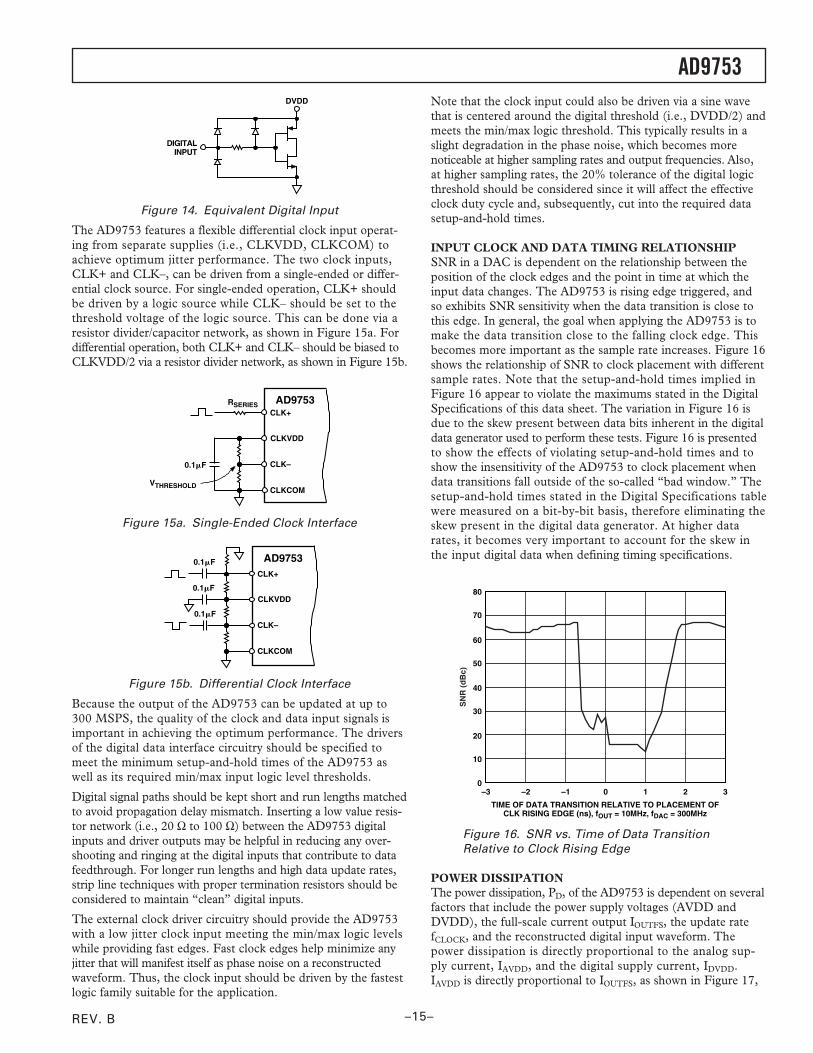
INPUT CLOCK AND DATA TIMING RELATIONSHIPSNR in a DAC is dependent on the relationship between theposition of the clock edges and the point in time at which theinput data changes. The AD9753 is rising edge triggered, andso exhibits SNR sensitivity when the data transition is close tothis edge. In general, the goal when applying the AD9753 is tomake the data transition close to the falling clock edge. Thisbecomes more important as the sample rate increases. Figure 16shows the relationship of SNR to clock placement with differentsample rates. Note that the setup-and-hold times implied inFigure 16 appear to violate the maximums stated in the DigitalSpecifications of this data sheet. The variation in Figure 16 isdue to the skew present between data bits inherent in the digitaldata generator used to perform these tests. Figure 16 is presentedto show the effects of violating setup-and-hold times and toshow the insensitivity of the AD9753 to clock placement whendata transitions fall outside of the so-called “bad window.” Thesetup-and-hold times stated in the Digital Specifications tablewere measured on a bit-by-bit basis, therefore eliminating theskew present in the digital data generator. At higher datarates, it becomes very important to account for the skew inthe input digital data when defining timing specifications.
TIME OF DATA TRANSITION RELATIVE TO PLACEMENT OFCLK RISING EDGE (ns), fOUT = 10MHz, fDAC = 300MHz
80
40
030–3
SN
R (
dB
c)
60
20
70
30
50
10
–2 –1 1 2
Figure 16. SNR vs. Time of Data TransitionRelative to Clock Rising Edge
POWER DISSIPATIONThe power dissipation, PD, of the AD9753 is dependent on severalfactors that include the power supply voltages (AVDD andDVDD), the full-scale current output IOUTFS, the update ratefCLOCK, and the reconstructed digital input waveform. Thepower dissipation is directly proportional to the analog sup-ply current, IAVDD, and the digital supply current, IDVDD.IAVDD is directly proportional to IOUTFS, as shown in Figure 17,
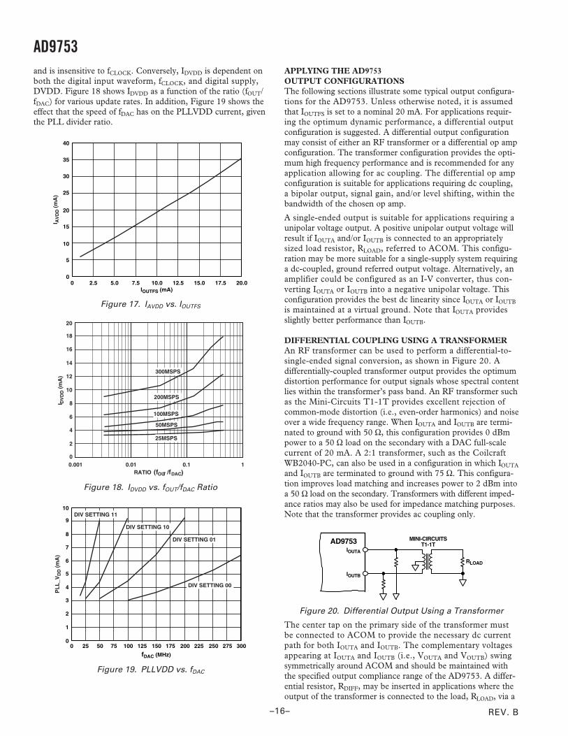
REV. B–16–
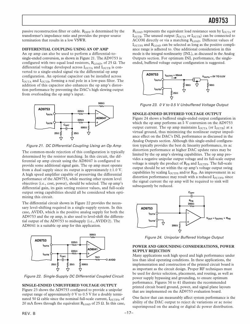
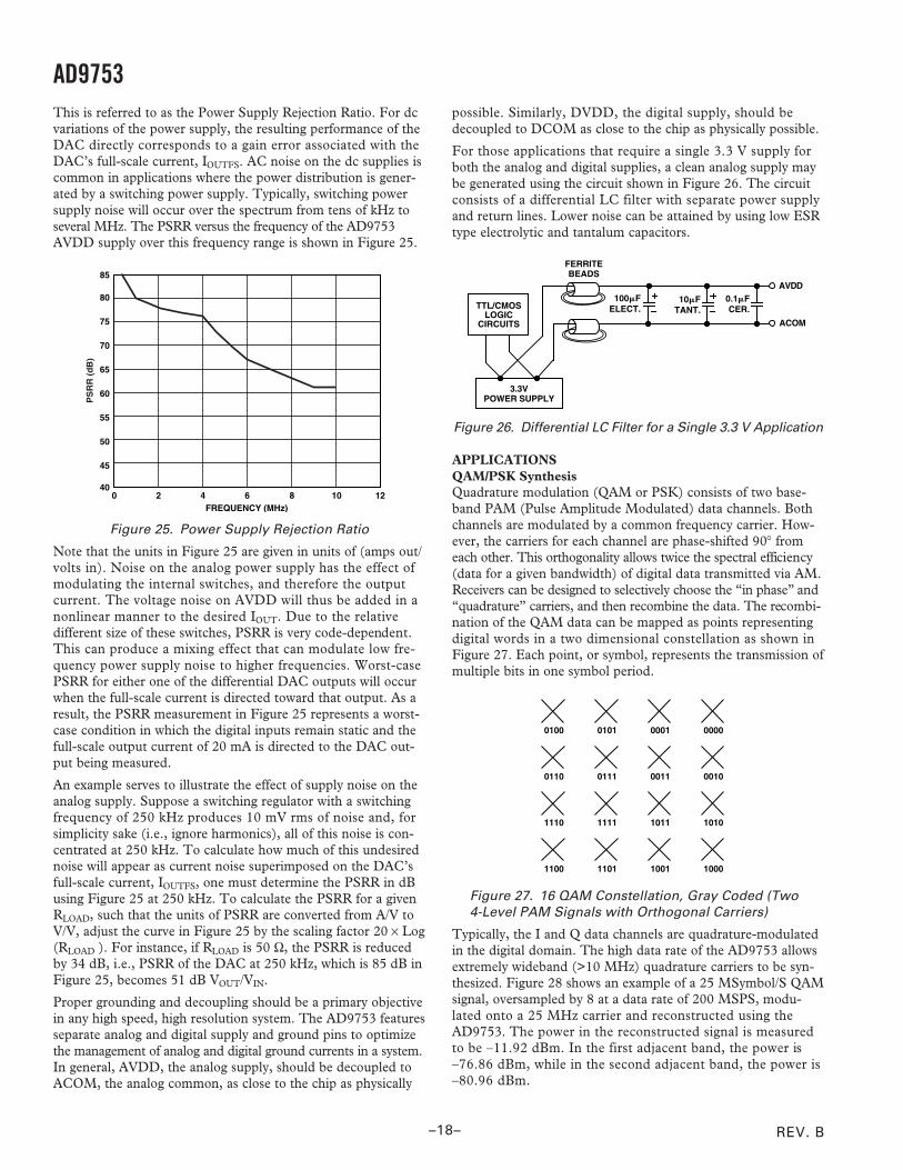
AD9753and is insensitive to fCLOCK. Conversely, IDVDD is dependent onboth the digital input waveform, fCLOCK, and digital supply,DVDD. Figure 18 shows IDVDD as a function of the ratio (fOUT/fDAC) for various update rates. In addition, Figure 19 shows theeffect that the speed of fDAC has on the PLLVDD current, giventhe PLL divider ratio.
IOUTFS (mA)
40
20
020.010.00
I AV
DD
(m
A)
35
10
30
25
15
5
2.5 5.0 7.5 12.5 15.0 17.5
Figure 17. IAVDD vs. IOUTFS
RATIO (fOUT /fDAC
20
16
010.010.001
I DV
DD
(m
A)
18
14
12
10
8
6
4
2
0.1
300MSPS
200MSPS
100MSPS
50MSPS
25MSPS
)
Figure 18. IDVDD vs. fOUT/fDAC Ratio
fDAC (MHz)
10
03001500
PL
L_V
DD
(m
A)
9
8
7
6
5
4
3
2
50 100 200 250
1
17525 75 125 225 275
DIV SETTING 00
DIV SETTING 11
DIV SETTING 10
DIV SETTING 01
Figure 19. PLLVDD vs. fDAC
APPLYING THE AD9753OUTPUT CONFIGURATIONSThe following sections illustrate some typical output configura-tions for the AD9753. Unless otherwise noted, it is assumedthat IOUTFS is set to a nominal 20 mA. For applications requir-ing the optimum dynamic performance, a differential outputconfiguration is suggested. A differential output configurationmay consist of either an RF transformer or a differential op ampconfiguration. The transformer configuration provides the opti-mum high frequency performance and is recommended for anyapplication allowing for ac coupling. The differential op ampconfiguration is suitable for applications requiring dc coupling,a bipolar output, signal gain, and/or level shifting, within thebandwidth of the chosen op amp.
A single-ended output is suitable for applications requiring aunipolar voltage output. A positive unipolar output voltage willresult if IOUTA and/or IOUTB is connected to an appropriatelysized load resistor, RLOAD, referred to ACOM. This configu-ration may be more suitable for a single-supply system requiringa dc-coupled, ground referred output voltage. Alternatively, anamplifier could be configured as an I-V converter, thus con-verting IOUTA or IOUTB into a negative unipolar voltage. Thisconfiguration provides the best dc linearity since IOUTA or IOUTB
is maintained at a virtual ground. Note that IOUTA providesslightly better performance than IOUTB.
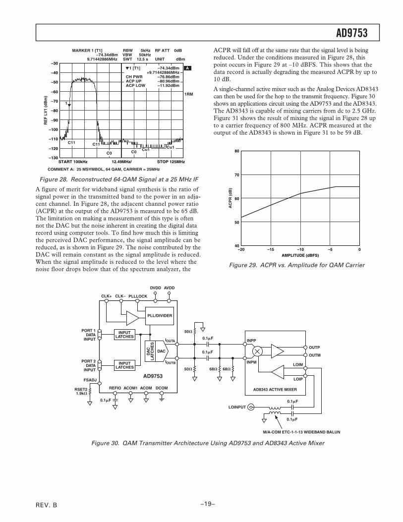
DIFFERENTIAL COUPLING USING A TRANSFORMERAn RF transformer can be used to perform a differential-to-single-ended signal conversion, as shown in Figure 20. Adifferentially-coupled transformer output provides the optimumdistortion performance for output signals whose spectral contentlies within the transformer’s pass band. An RF transformer suchas the Mini-Circuits T1-1T provides excellent rejection ofcommon-mode distortion (i.e., even-order harmonics) and noiseover a wide frequency range. When IOUTA and IOUTB are termi-nated to ground with 50 Ω, this configuration provides 0 dBmpower to a 50 Ω load on the secondary with a DAC full-scalecurrent of 20 mA. A 2:1 transformer, such as the CoilcraftWB2040-PC, can also be used in a configuration in which IOUTA
and IOUTB are terminated to ground with 75 Ω. This configura-tion improves load matching and increases power to 2 dBm intoa 50 Ω load on the secondary. Transformers with different imped-ance ratios may also be used for impedance matching purposes.Note that the transformer provides ac coupling only.
RLOAD
AD9753 MINI-CIRCUITST1-1T
IOUTA
IOUTB
Figure 20. Differential Output Using a Transformer
The center tap on the primary side of the transformer mustbe connected to ACOM to provide the necessary dc currentpath for both IOUTA and IOUTB. The complementary voltagesappearing at IOUTA and IOUTB (i.e., VOUTA and VOUTB) swingsymmetrically around ACOM and should be maintained withthe specified output compliance range of the AD9753. A differ-ential resistor, RDIFF, may be inserted in applications where theoutput of the transformer is connected to the load, RLOAD, via a
REV. B
AD9753
–17–
passive reconstruction filter or cable. RDIFF is determined by thetransformer’s impedance ratio and provides the proper sourcetermination that results in a low VSWR.
DIFFERENTIAL COUPLING USING AN OP AMPAn op amp can also be used to perform a differential-to-single-ended conversion, as shown in Figure 21. The AD9753 isconfigured with two equal load resistors, RLOAD, of 25 Ω. Thedifferential voltage developed across IOUTA and IOUTB is con-verted to a single-ended signal via the differential op ampconfiguration. An optional capacitor can be installed acrossIOUTA and IOUTB, forming a real pole in a low-pass filter. Theaddition of this capacitor also enhances the op amp’s distor-tion performance by preventing the DAC’s high slewing outputfrom overloading the op amp’s input.
AD9753IOUTA
IOUTBCOPT
500
225
225
500
2525
AD8047
Figure 21. DC Differential Coupling Using an Op Amp
The common-mode rejection of this configuration is typicallydetermined by the resistor matching. In this circuit, the dif-ferential op amp circuit using the AD8047 is configured toprovide some additional signal gain. The op amp must operatefrom a dual supply since its output is approximately ± 1.0 V.A high speed amplifier capable of preserving the differentialperformance of the AD9753, while meeting other system levelobjectives (i.e., cost, power), should be selected. The op amp’sdifferential gain, its gain setting resistor values, and full-scaleoutput swing capabilities should all be considered when opti-mizing this circuit.
The differential circuit shown in Figure 22 provides the neces-sary level-shifting required in a single-supply system. In thiscase, AVDD, which is the positive analog supply for both theAD9753 and the op amp, is also used to level-shift the differen-tial output of the AD9753 to midsupply (i.e., AVDD/2). TheAD8041 is a suitable op amp for this application.
AD9753IOUTA
IOUTB COPT
500
225
225
5002525
AD8041
1kAVDD
Figure 22. Single-Supply DC Differential Coupled Circuit
SINGLE-ENDED UNBUFFERED VOLTAGE OUTPUTFigure 23 shows the AD9753 configured to provide a unipolaroutput range of approximately 0 V to 0.5 V for a doubly termi-nated 50 Ω cable since the nominal full-scale current, IOUTFS, of20 mA flows through the equivalent RLOAD of 25 Ω. In this case,
RLOAD represents the equivalent load resistance seen by IOUTA orIOUTB. The unused output (IOUTA or IOUTB) can be connected toACOM directly or via a matching RLOAD. Different values ofIOUTFS and RLOAD can be selected as long as the positive compli-ance range is adhered to. One additional consideration in thismode is the integral nonlinearity (INL), as discussed in the AnalogOutputs section. For optimum INL performance, the single-ended, buffered voltage output configuration is suggested.
AD9753IOUTA
IOUTB
50
25
50
VOUTA = 0V TO 0.5VIOUTFS = 20mA
Figure 23. 0 V to 0.5 V Unbuffered Voltage Output
SINGLE-ENDED BUFFERED VOLTAGE OUTPUTFigure 24 shows a buffered single-ended output configuration inwhich the op amp performs an I–V conversion on the AD9753output current. The op amp maintains IOUTA (or IOUTB) at avirtual ground, thus minimizing the nonlinear output imped-ance effect on the DAC’s INL performance as discussed in theAnalog Outputs section. Although this single-ended configura-tion typically provides the best dc linearity performance, its acdistortion performance at higher DAC update rates may belimited by the op amp’s slewing capabilities. The op amp pro-vides a negative unipolar output voltage and its full-scale outputvoltage is simply the product of RFB and IOUTFS. The full-scaleoutput should be set within the op amp’s voltage output swingcapabilities by scaling IOUTFS and/or RFB. An improvement in acdistortion performance may result with a reduced IOUTFS, sincethe signal current the op amp will be required to sink willsubsequently be reduced.
AD9753IOUTA
IOUTB
COPT
200
VOUT = IOUTFS RFB
RFB200
Figure 24. Unipolar Buffered Voltage Output
POWER AND GROUNDING CONSIDERATIONS, POWERSUPPLY REJECTIONMany applications seek high speed and high performance underless than ideal operating conditions. In these applications, theimplementation and construction of the printed circuit board isas important as the circuit design. Proper RF techniques mustbe used for device selection, placement, and routing, as well aspower supply bypassing and grounding, to ensure optimumperformance. Figures 34 to 41 illustrate the recommendedprinted circuit board ground, power, and signal plane layoutsthat are implemented on the AD9753 evaluation board.
One factor that can measurably affect system performance is theability of the DAC output to reject dc variations or ac noisesuperimposed on the analog or digital dc power distribution.
REV. B–18–
AD9753This is referred to as the Power Supply Rejection Ratio. For dcvariations of the power supply, the resulting performance of theDAC directly corresponds to a gain error associated with theDAC’s full-scale current, IOUTFS. AC noise on the dc supplies iscommon in applications where the power distribution is gener-ated by a switching power supply. Typically, switching powersupply noise will occur over the spectrum from tens of kHz toseveral MHz. The PSRR versus the frequency of the AD9753AVDD supply over this frequency range is shown in Figure 25.
FREQUENCY (MHz)
85
401260
PS
RR
(d
B)
80
75
70
65
60
55
50
45
2 4 8 10
Figure 25. Power Supply Rejection Ratio
Note that the units in Figure 25 are given in units of (amps out/volts in). Noise on the analog power supply has the effect ofmodulating the internal switches, and therefore the outputcurrent. The voltage noise on AVDD will thus be added in anonlinear manner to the desired IOUT. Due to the relativedifferent size of these switches, PSRR is very code-dependent.This can produce a mixing effect that can modulate low fre-quency power supply noise to higher frequencies. Worst-casePSRR for either one of the differential DAC outputs will occurwhen the full-scale current is directed toward that output. As aresult, the PSRR measurement in Figure 25 represents a worst-case condition in which the digital inputs remain static and thefull-scale output current of 20 mA is directed to the DAC out-put being measured.
An example serves to illustrate the effect of supply noise on theanalog supply. Suppose a switching regulator with a switchingfrequency of 250 kHz produces 10 mV rms of noise and, forsimplicity sake (i.e., ignore harmonics), all of this noise is con-centrated at 250 kHz. To calculate how much of this undesirednoise will appear as current noise superimposed on the DAC’sfull-scale current, IOUTFS, one must determine the PSRR in dBusing Figure 25 at 250 kHz. To calculate the PSRR for a givenRLOAD, such that the units of PSRR are converted from A/V toV/V, adjust the curve in Figure 25 by the scaling factor 20 × Log(RLOAD ). For instance, if RLOAD is 50 Ω, the PSRR is reducedby 34 dB, i.e., PSRR of the DAC at 250 kHz, which is 85 dB inFigure 25, becomes 51 dB VOUT/VIN.
Proper grounding and decoupling should be a primary objectivein any high speed, high resolution system. The AD9753 featuresseparate analog and digital supply and ground pins to optimizethe management of analog and digital ground currents in a system.In general, AVDD, the analog supply, should be decoupled toACOM, the analog common, as close to the chip as physically
possible. Similarly, DVDD, the digital supply, should bedecoupled to DCOM as close to the chip as physically possible.
For those applications that require a single 3.3 V supply forboth the analog and digital supplies, a clean analog supply maybe generated using the circuit shown in Figure 26. The circuitconsists of a differential LC filter with separate power supplyand return lines. Lower noise can be attained by using low ESRtype electrolytic and tantalum capacitors.
AVDD
ACOM
100FELECT.
10FTANT.
0.1FCER.TTL/CMOS
LOGICCIRCUITS
3.3VPOWER SUPPLY
FERRITEBEADS
Figure 26. Differential LC Filter for a Single 3.3 V Application
APPLICATIONSQAM/PSK SynthesisQuadrature modulation (QAM or PSK) consists of two base-band PAM (Pulse Amplitude Modulated) data channels. Bothchannels are modulated by a common frequency carrier. How-ever, the carriers for each channel are phase-shifted 90° fromeach other. This orthogonality allows twice the spectral efficiency(data for a given bandwidth) of digital data transmitted via AM.Receivers can be designed to selectively choose the “in phase” and“quadrature” carriers, and then recombine the data. The recombi-nation of the QAM data can be mapped as points representingdigital words in a two dimensional constellation as shown inFigure 27. Each point, or symbol, represents the transmission ofmultiple bits in one symbol period.
0100 0101 0001 0000
0110 0111 0011 0010
1110 1111 1011 1010
1100 1101 1001 1000
Figure 27. 16 QAM Constellation, Gray Coded (Two4-Level PAM Signals with Orthogonal Carriers)
Typically, the I and Q data channels are quadrature-modulatedin the digital domain. The high data rate of the AD9753 allowsextremely wideband (>10 MHz) quadrature carriers to be syn-thesized. Figure 28 shows an example of a 25 MSymbol/S QAMsignal, oversampled by 8 at a data rate of 200 MSPS, modu-lated onto a 25 MHz carrier and reconstructed using theAD9753. The power in the reconstructed signal is measuredto be –11.92 dBm. In the first adjacent band, the power is–76.86 dBm, while in the second adjacent band, the power is–80.96 dBm.
REV. B
AD9753
–19–
–30
START 100kHz
–40
–50
–60
–70
–80
–90
–100
–110
–120
–13012.49MHz/ STOP 125MHz
RE
F LV
1 (d
Bm
) 1RM
–74.34dBm+9.71442886MHz
–76.86dBm–80.96dBm–11.92dBm
1 [T1]
CH PWRACP UPACP LOW
C11
C0Cu1
C11
C0Cu1
MARKER 1 [T1] RBW 5kHz RF ATT 0dB –74.34dBm VBW 50kHz 9.71442886MHz SWT 12.5 s UNIT dBm
COMMENT A: 25 MSYMBOL, 64 QAM, CARRIER = 25MHz
1
Figure 28. Reconstructed 64-QAM Signal at a 25 MHz IF
A figure of merit for wideband signal synthesis is the ratio ofsignal power in the transmitted band to the power in an adja-cent channel. In Figure 28, the adjacent channel power ratio(ACPR) at the output of the AD9753 is measured to be 65 dB.The limitation on making a measurement of this type is oftennot the DAC but the noise inherent in creating the digital datarecord using computer tools. To find how much this is limitingthe perceived DAC performance, the signal amplitude can bereduced, as is shown in Figure 29. The noise contributed by theDAC will remain constant as the signal amplitude is reduced.When the signal amplitude is reduced to the level where thenoise floor drops below that of the spectrum analyzer, the
ACPR will fall off at the same rate that the signal level is beingreduced. Under the conditions measured in Figure 28, thispoint occurs in Figure 29 at –10 dBFS. This shows that thedata record is actually degrading the measured ACPR by up to10 dB.
A single-channel active mixer such as the Analog Devices AD8343can then be used for the hop to the transmit frequency. Figure 30shows an applications circuit using the AD9753 and the AD8343.The AD8343 is capable of mixing carriers from dc to 2.5 GHz.Figure 31 shows the result of mixing the signal in Figure 28 upto a carrier frequency of 800 MHz. ACPR measured at theoutput of the AD8343 is shown in Figure 31 to be 59 dB.
AMPLITUDE (dBFS)
80
60
400–10–20
AC
PR
(d
B)
70
50
–15 –5
Figure 29. ACPR vs. Amplitude for QAM Carrier
DA
CL
ATC
HE
S
DAC
INPUTLATCHES
INPUTLATCHES
PLL/DIVIDER
CLK+ CLK– PLLLOCK
DVDD AVDD
IOUTA
IOUTB
PORT 1DATA
INPUT
PORT 2DATA
INPUT
RSET21.9k
FSADJ
0.1F
REFIO ACOM1 ACOM DCOM
AD9753
50
50
0.1F
0.1F
68 68
INPM
INPP
LOIM
LOIP
OUTP
OUTM
AD8343 ACTIVE MIXER
0.1F
0.1F
LOINPUT
M/A-COM ETC-1-1-13 WIDEBAND BALUN
Figure 30. QAM Transmitter Architecture Using AD9753 and AD8343 Active Mixer

REV. B–20–
AD9753
–20
CENTER 860MHz
–30
–40
–50
–60
–70
–80
–90
–100
–110
–12011MHz/ SPAN 110MHz
RE
F L
V1
(dB
m) 2MA
MARKER 1 [T2] RBW 10kHz RF ATT 0dB –99.88dBm VBW 10kHz 859.91983968MHz SWT 2.8 s UNIT dBm
COMMENT A: 25 MSYMBOL, 64 QAM CARRIER @ 825MHz
–99.88bBm,+859.91983968MHz
–65.67dBm–65.15dBm–7.05dBm
33.10dB–49.91983968MHz
33.10dB–49.91983968MHz
1 [T2]
CH PWRACP UPACP LOW 1 [T2]
2 [T2]
C11 C11
C0 C0Cu1 Cu1
1
12
Figure 31. Signal of Figure 28 Mixed to CarrierFrequency of 800 MHz
Effects of Noise and Distortion on Bit Error Rate (BER)Textbook analyses of Bit Error Rate (BER) performance aregenerally stated in terms of E (energy in watts-per-symbol orwatts-per-bit) and NO (spectral noise density in watts/Hz).For QAM signals, this performance is shown graphically inFigure 32. M represents the number of levels in each quadra-ture PAM signal (i.e., M = 8 for 64 QAM, M = 16 for 256 QAM).Figure 32 implies gray coding in the QAM constellation, as wellas the use of matched filters at the receiver, which is typical.The horizontal axis of Figure 32 can be converted to units ofenergy/symbol by adding to the horizontal axis 10 log of thenumber of bits in the desired curve. For instance, to achieve aBER of 1e-6 with 64 QAM, an energy per bit of 20 dB is neces-sary. To calculate energy per symbol, we add 10 log(6), or7.8 dB. 64 QAM with a BER of 1e-6 (assuming no source orchannel coding) can therefore theoretically be achieved withan energy/symbol-to-noise (E/NO) ratio of 27.8 dB. Due to theloss and interferers inherent in the wireless path, this signal-to-noise ratio must be realized at the receiver to achieve the givenbit error rate.
Distortion effects on BER are much more difficult to determineaccurately. Most often in simulation, the energies of the strongestdistortion components are root-sum-squared with the noise, andthe result is treated as if it were all noise. That being said, if theexample above of 64 QAM with the BER of 1e-6, using theE/NO ratio is much greater than the worst-case SFDR, the noisewill dominate the BER calculation.
The AD9753 has a worst-case in-band SFDR of 47 dB at theupper end of its frequency spectrum (see TPCs 4 and 7). Whenused to synthesize high level QAM signals as described above,noise, as opposed to distortion, will dominate its performance inthese applications.
SNR/BIT (dB)
1E–0
1E–3
1E–62050
SY
MB
OL
ER
RO
R P
RO
BA
BIL
ITY
1E–2
1E–5
1E–1
1E–4
10 15
16 QAM 64 QAM4 QAM
20
Figure 32. Probability of a Symbol Error for QAM
Pseudo Zero Stuffing/IF ModeThe excellent dynamic range of the AD9753 allows its use inapplications where synthesis of multiple carriers is desired. Inaddition, the AD9753 can be used in a pseudo zero stuffingmode that improves dynamic range at IF frequencies. In thismode, data from the two input channels is interleaved to theDAC, which is running at twice the speed of either of the inputports. However, the data at Port 2 is held constant at midscale.The effect of this is shown in Figure 33. The IF signal is theimage, with respect to the input data rate, of the fundamen-tal. Normally, the sinx/x response of the DAC will attenuatethis image. Zero stuffing improves the pass-band flatness so thatthe image amplitude is closer to that of the fundamental sig-nal. Zero stuffing can be an especially useful technique in thesynthesis of IF signals.
FREQUENCY (Normalized to Input Data Rate)
0
–30
20.50
EF
FE
CT
OF
SIN
X/X
RO
LL
-OF
F
–20
–50
–10
–40
1 1.5
AMPLITUDEOF IMAGEWITHOUT
ZERO STUFFING
AMPLITUDEOF IMAGEUSINGZERO STUFFING
Figure 33. Effects of Pseudo Zero Stuffing onSpectrum of AD9753
REV. B
AD9753
–21–
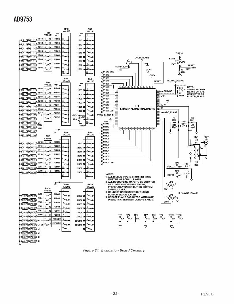
EVALUATION BOARDThe AD9753-EB is an evaluation board for the AD9753 TxDAC.Careful attention to layout and circuit design, combined withprototyping area, allows the user to easily and effectively evalu-ate the AD9753 in different modes of operation.
Referring to Figures 34 and 35, the AD9753’s performance canbe evaluated differentially or single-ended either using a trans-former, or directly coupling the output. To evaluate the outputdifferentially using the transformer, it is recommended thateither the Mini-Circuits T1-1T (through-hole) or the CoilcraftTTWB-1-B (SMT) be placed in the position of T1 on the evalua-tion board. To evaluate the output either single-ended or direct-coupled, remove the transformer and bridge either BL1 or BL2.
The digital data to the AD9753 comes from two ribbon cables thatinterface to the 40-lead IDC connectors P1 and P2. Proper termi-nation or voltage scaling can be accomplished by installing theresistor pack networks RN1–RN12. RN1, 4, 7, and 10 are 22 ΩDIP resistor packs and should be installed as they help reduce thedigital edge rates and therefore peak current on the inputs.
A single-ended clock can be applied via J3. By setting the SE/DIFF labeled jumpers J2, 3, 4, and 6, the input clock can bedirected to the CLK+/CLK– inputs of the AD9753 in either asingle-ended or differential manner. If a differentially appliedclock is desired, a Mini-Circuits T1-1T transformer should beused in the position of T2. Note that with a single-ended square
wave clock input, T2 must be removed. A clock can also beapplied via the ribbon cable on Port 1 (P1), Pin 33. By insertingthe EDGE jumper (JP1), this clock will be applied to the CLK+input of the AD9753. JP3 should be set in its SE position in thisapplication to bias CLK– to 1/2 the supply voltage.
The AD9753’s PLL clock multiplier can be enabled by insertingJP7 in the IN position. As described in the Typical PerformanceCharacteristics and Functional Description sections, with the PLLenabled, a clock at 1/2 the output data rate should be applied asdescribed in the last paragraph. The PLL takes care of the internal2× frequency multiplication and all internal timing requirements.In this application, the PLLLOCK output indicates when lockis achieved on the PLL. With the PLL enabled, the DIV0 andDIV1 jumpers (JP8 and JP9) provide the PLL divider ratio asdescribed in Table I.
The PLL is disabled when JP7 is in the EX setting. In this mode, aclock at the speed of the output data rate must be applied to theclock inputs. Internally, the clock is divided by 2. For datasynchronization, a 1 clock is provided on the PLLLOCK pinin this application. Care should be taken to read the timingrequirements described earlier in the data sheet for optimumperformance. With the PLL disabled, the DIV0 and DIV1 jumpersdefine the mode (interleaved, noninterleaved) as described inTable II.
REV. B–22–
AD9753
1 162B132
4
6
8
12
10
16
14
P2
P2
P2
P2
P2
P2
P2
P2
P2B13
1
2 152B12 P2B12
2
3 142B11 P2B11
3
4 132B10 P2B10
4
5 122B09 P2B09
5
6 112B08 P2B08
6
7 102B07 P2B07
7
8 92B06 P2B06
8
9
10
RN8VALUE
RN7VALUE
P2
P2
P2
P2
P2
P2
P2
P2
1
3
5
7
9
11
13
15
1
2
3
4
5
6
7
8
9
10
2B13
2B12
2B11
2B10
2B09
2B08
2B07
2B06
RN9VALUE
1 161B132
4
6
8
12
10
16
14
P1
P1
P1
P1
P1
P1
P1
P1
P1B13
1
2 151B12 P1B12
2
3 141B11 P1B11
3
4 131B10 P1B10
4
5 121B09 P1B09
5
6 111B08 P1B08
6
7 101B07 P1B07
7
8 91B06 P1B06
8
9
10
RN2VALUE
RN1VALUE
P1
P1
P1
P1
P1
P1
P1
P1
11
13
15
1
3
5
7
9
1 161B0518
20
22
24
28
26
32
30
P1
P1
P1
P1
P1
P1
P1
P1
17
19
21
23
25
27
29
31
P1
P1
P1
P1
P1
P1
P1
P1
P1B05
1
2 151B04 P1B04
2
3 141B03 P1B03
3
4 131B02 P1B02
4
5 121B01 P1B01
5
6 111B00 P1B00
6
7 101O17 OUT15
7
8 9 OUT16
8
9
10
RN5VALUE
RN4VALUE
36
34
40
38
P1
P1
P1
P1
P1
P1
P1
P1
33
35
37
39
25 26 27 28 29 30 31 32 33 34 35 36
U1AD9751/AD9753/AD9755
48
47
46
45
44
43
42
41
40
39
38
37
13
14
15
1617
18
19
20
22
23
24
21
12 11 10 9 8 3 2 17 6 5 4
P2B12
MSBP2B13
P2B11P2B10P2B09P2B08P2B07P2B06P2B05P2B04P2B03P2B02P2B01P2B00 LSB
SP
1
2
3JP9
AVDD PLANE
1
2
3JP8
AVDD_PLANE
DIV0
DIV1
A B
A B
REFIO
FSADJ
C120.1F
WHT
TP2
WHT
TP1R1
1.91k
DVDD PLANE
P1B12P1B11P1B10P1B09P1B08P1B07P1B06P1B05P1B04
P1B03P1B02P1B01P1B00 LSB
P1B13 MSB
CLKVDD
IAIB
P
LPF
C111.0FR5392
R10OPT
4
61
2
3T1
BL1
BL2
1
2
IOUTJ5
1
2DGND: 3,4,5
J1DVDD PLANE
CLK+
CLK–
RESET
1
2
3
JP5
RESET
AB
R450
WHTTP3
OUT16
EDGE
EXT
R350
C1010pF
R250
C910pF
NOTE:SHIELD AROUNDR5 AND C11 ARECONNECTED TOPLLVDD PLANE
PLLVDD PLANE
1
2
3
4
5
6
7
8
9
10
1B13
1B12
1B11
1B10
1B09
1B08
1B07
1B06
RN3VALUE
1B05
1B04
1B03
1B02
1B01
1B00
1O16
RN6VALUE
1
2
3
4
5
6
7
8
9
10
1O17
1O15
JP10
BLK
TP4
BLK
TP5
BLK
TP6
1 162B0518
20
22
24
28
26
32
30
P2
P2
P2
P2
P2
P2
P2
P2
17
19
21
23
25
27
29
31
P2
P2
P2
P2
P2
P2
P2
P2
P2B05
1
2 152B04 P2B04
2
3 142B03 P2B03
3
4 132B02 P2B02
4
5 122B01 P2B01
5
6 112B00 P2B00
6
7 10
7
8 9
8
9
10
RN11VALUE
RN10VALUE
36
34
40
38
P2
P2
P2
P2
P2
P2
P2
P2
33
35
37
39
P2OUT15
P2OUT16
2B05
2B04
2B03
2B02
2B01
2B00
RN12VALUE
1
2
3
4
5
6
7
8
9
10
2OUT15
2OUT16
NOTES1. ALL DIGITAL INPUTS FROM RN1–RN12 MUST BE OF EQUAL LENGTH.2. ALL DECOUPLING CAPS TO BE LOCATED AS CLOSE AS POSSIBLE TO DUT, PREFERABLY UNDER DUT ON BOTTOM SIGNAL LAYER.3. CONNECT GNDS UNDER DUT USING BOTTOM SIGNAL LAYER.4. CREATE PLANE CAPACITOR WITH 0.007" DIELECTRIC BETWEEN LAYERS 2 AND 3.
BLK
TP7
BLK
TP8
BLK
TP9
P
BLK
TP10
BLK
TP12
1O15
1O16
Figure 34. Evaluation Board Circuitry

REV. B
AD9753
–23–
SP
4
6
1
2
3T2
1
2
12
3
JP6
CLK+
AB
C160.1F P
R91k
JP4
DFJ3
CLK
P
1
2
3
JP2AB
SE
DF
JP1EDGE
OUT15
CKLVDD
R71k
P
1
2
3
JP3AB
SE
DF
PGND: 3, 4, 5P
R850
CLK–
C1310F10V
TP13
DVDD PLANE
BLK
P
DVDD
J8
L1FBEAD
1 1 2
TP14
RED
DGND
J91
C1410F10V
TP15
AVDD PLANE
BLK
AVDD
J10
L2FBEAD
1 1 2
TP16
RED
AGND
J111
C1510F10V
TP17
CLKVDD
BLK
CLKVDD
J12
L3FBEAD
1 1 2
TP11
RED
CLKGND
J131
12
3
JP7A
BPLLVDD PLANE
C10.1F
DVDD PLANEPINS 5, 6
C21F
C30.1F
C41F
PINS 21, 22
C50.1F
PINS 41, 44
C61F
AVDD PLANE
C70.1F
PINS 45, 47
C81F
CLKVDD
P
U1 BYPASS CAPS
Figure 35. Evaluation Board Clock Circuitry

REV. B–24–
AD9753
Figure 36. Evaluation Board, Assembly—Top
Figure 37. Evaluation Board, Assembly—Bottom

REV. B
AD9753
–25–
Figure 38. Evaluation Board, Top Layer
Figure 39. Evaluation Board, Layer 2, Ground Plane
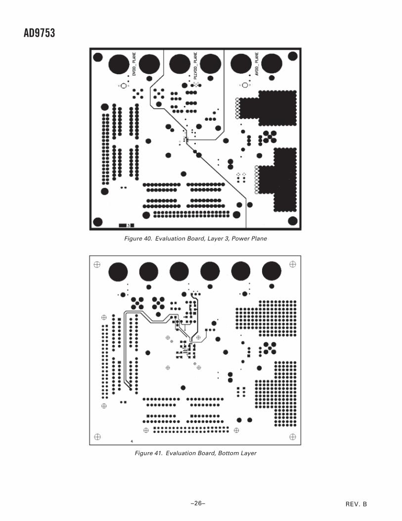
REV. B–26–
AD9753
Figure 40. Evaluation Board, Layer 3, Power Plane
Figure 41. Evaluation Board, Bottom Layer
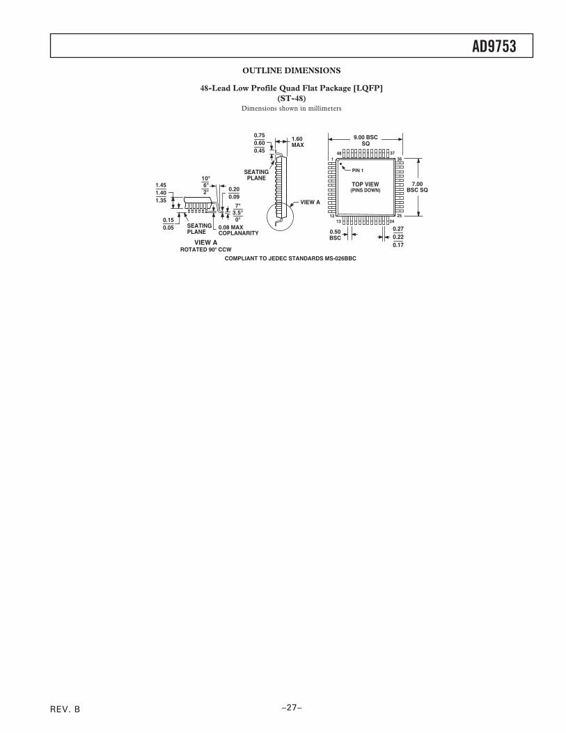
REV. B
AD9753
–27–
OUTLINE DIMENSIONS
48-Lead Low Profile Quad Flat Package [LQFP](ST-48)
Dimensions shown in millimeters
TOP VIEW(PINS DOWN)
1
1213
2524
363748
0.27 0.22 0.17
0.50BSC
7.00BSC SQ
SEATINGPLANE
1.60MAX
0.750.600.45
VIEW A
9.00 BSCSQ
PIN 1
0.20 0.09
1.45 1.40 1.35
0.08 MAXCOPLANARITY
VIEW AROTATED 90 CCW
SEATINGPLANE
1062
73.500.15
0.05
COMPLIANT TO JEDEC STANDARDS MS-026BBC
REV. B–28–
C02
251–
0–9/
03(B
)
AD9753
Revision HistoryLocation Page
9/03—Data Sheet changed from REV. A to REV. B.
Changes to GENERAL DESCRIPTION . . . . . . . . . . . . . . . . . . . . . . . . . . . . . . . . . . . . . . . . . . . . . . . . . . . . . . . . . . . . . . . . . . . . . 1
Changes to PRODUCT HIGHLIGHTS . . . . . . . . . . . . . . . . . . . . . . . . . . . . . . . . . . . . . . . . . . . . . . . . . . . . . . . . . . . . . . . . . . . . . . 1
Changes to DIGITAL SPECIFICATIONS . . . . . . . . . . . . . . . . . . . . . . . . . . . . . . . . . . . . . . . . . . . . . . . . . . . . . . . . . . . . . . . . . . . 4
Changes to ORDERING GUIDE . . . . . . . . . . . . . . . . . . . . . . . . . . . . . . . . . . . . . . . . . . . . . . . . . . . . . . . . . . . . . . . . . . . . . . . . . . . 5
Changes to Figure 2 . . . . . . . . . . . . . . . . . . . . . . . . . . . . . . . . . . . . . . . . . . . . . . . . . . . . . . . . . . . . . . . . . . . . . . . . . . . . . . . . . . . . . . 7
Changes to Figure 3 . . . . . . . . . . . . . . . . . . . . . . . . . . . . . . . . . . . . . . . . . . . . . . . . . . . . . . . . . . . . . . . . . . . . . . . . . . . . . . . . . . . . . 10
Changes to FUNCTIONAL DESCRIPTION section . . . . . . . . . . . . . . . . . . . . . . . . . . . . . . . . . . . . . . . . . . . . . . . . . . . . . . . . . . 10
Changes to Figure 6 . . . . . . . . . . . . . . . . . . . . . . . . . . . . . . . . . . . . . . . . . . . . . . . . . . . . . . . . . . . . . . . . . . . . . . . . . . . . . . . . . . . . . 11
Changes to Figure 9 . . . . . . . . . . . . . . . . . . . . . . . . . . . . . . . . . . . . . . . . . . . . . . . . . . . . . . . . . . . . . . . . . . . . . . . . . . . . . . . . . . . . . 12
Changes to Figure DIGITAL INPUTS section . . . . . . . . . . . . . . . . . . . . . . . . . . . . . . . . . . . . . . . . . . . . . . . . . . . . . . . . . . . . . . . . 14
Changes to Figure 34 . . . . . . . . . . . . . . . . . . . . . . . . . . . . . . . . . . . . . . . . . . . . . . . . . . . . . . . . . . . . . . . . . . . . . . . . . . . . . . . . . . . . 22
1/03—Data Sheet changed from REV. 0 to REV. A.
Changes to DIGITAL SPECIFICATIONS . . . . . . . . . . . . . . . . . . . . . . . . . . . . . . . . . . . . . . . . . . . . . . . . . . . . . . . . . . . . . . . . . . . 4
Changes to Figure 1 . . . . . . . . . . . . . . . . . . . . . . . . . . . . . . . . . . . . . . . . . . . . . . . . . . . . . . . . . . . . . . . . . . . . . . . . . . . . . . . . . . . . . . 5
Changes to Figure 2 . . . . . . . . . . . . . . . . . . . . . . . . . . . . . . . . . . . . . . . . . . . . . . . . . . . . . . . . . . . . . . . . . . . . . . . . . . . . . . . . . . . . . . 7
Changes to Figure 11 . . . . . . . . . . . . . . . . . . . . . . . . . . . . . . . . . . . . . . . . . . . . . . . . . . . . . . . . . . . . . . . . . . . . . . . . . . . . . . . . . . . . 13
Updated OUTLINE DIMENSIONS . . . . . . . . . . . . . . . . . . . . . . . . . . . . . . . . . . . . . . . . . . . . . . . . . . . . . . . . . . . . . . . . . . . . . . . 27