1 Reconfigurable Computing Lab UCLA FPGA Polyphase Filter Bank Study & Implementation Raghu Rao...
49
1 Reconfigurable Computing Lab UCLA FPGA Polyphase Filter Bank Study & Implementation Raghu Rao Matthieu Tisserand Mike Severa Prof. John Villasenor Image Communications/Reconfigurable Computing Lab. Electrical Engineering Dept. UCLA
-
Upload
sarahi-satterlee -
Category
Documents
-
view
217 -
download
2
Transcript of 1 Reconfigurable Computing Lab UCLA FPGA Polyphase Filter Bank Study & Implementation Raghu Rao...
1Reconfigurable Computing Lab
UCLA
FPGA Polyphase Filter Bank Study & Implementation
Raghu RaoMatthieu Tisserand
Mike SeveraProf. John Villasenor
Image Communications/Reconfigurable Computing Lab.Electrical Engineering Dept.
UCLA
2Reconfigurable Computing Lab
UCLAIntroduction
This document describes a polyphase filter bank and summarizes the results of a feasibility study of its implementation on FPGA-based architectures with respect to size, timing and bandwidth requirements
Under the SLAAC program, UCLA and Los Alamos National Labs have collaborated in mapping new adaptive algorithms to configurable computing platforms
3Reconfigurable Computing Lab
UCLAProject Goals
The current portion of the collaboration has involved the feasibilty and implementation of a Polyphase Filter bank using various FPGAs and hardware architectures.
The Polyphase implementation is a multi-rate filter structure combined with a DFT designed to extract subbands from an input signal
It is an optimization of the standard approaches and offers increased efficiency in both size and speed, aspects that are well suited to reconfigurable computing
Task heretofore implemented only in ASIC; offers a good opportunity as an example of migration from ASIC to an Adaptive platform

4Reconfigurable Computing Lab
UCLABasic Project Parameters
• 128 Megasamples/sec input signal
• 16 distinct subband outputs
• Implement using Polyphase filter and DFT structure
Poly-DFT128 Mss

5Reconfigurable Computing Lab
UCLA
FFT
COMMUTATOR
Polyphase filter bank
16 positive frequency bins
Input samples
Polyphase Filter Architecture

6Reconfigurable Computing Lab
UCLAPolyphase Filter Architecture
Commutator:• distributes signal to n lines• reduces clock speed by factor of n
Polyphase Filter bank:• 32 1-input, 1-output polyphase filters or • 16 1-input, 2-output optimized polyphase filters
FFT:• 2n-point real FFT• n-point complex FFT

7Reconfigurable Computing Lab
UCLASystem Requirements
Poly-DFT
8 to 16 bits@ 32MHz
8 to 16 bits@ 32MHz
• 128MHz system speed• Note: 4 samples at 32MHz equivalent to one sample at 128 MHz• All lines are buses equal to sample precision (from 8 to 16 bits)• Precision has been implemented as a generic in VHDL
• makes precision configurable• allows easy assessment of precision’s affect on feasibility
8Reconfigurable Computing Lab
UCLAWhat Happens Inside?
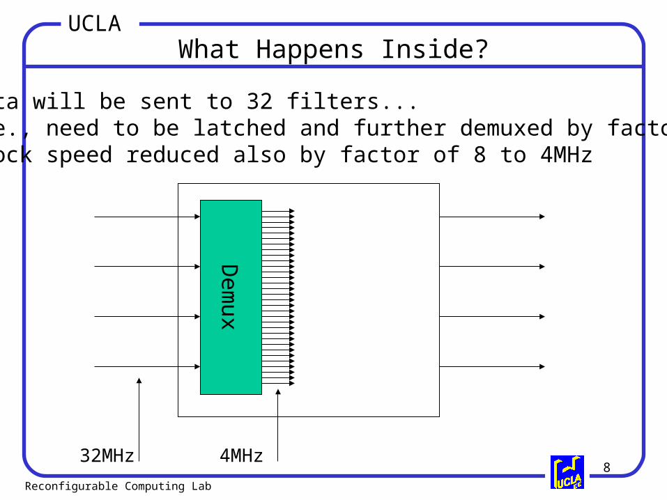
•Data will be sent to 32 filters...•i.e., need to be latched and further demuxed by factor of 8•Clock speed reduced also by factor of 8 to 4MHz
Dem
ux32MHz 4MHz
9Reconfigurable Computing Lab
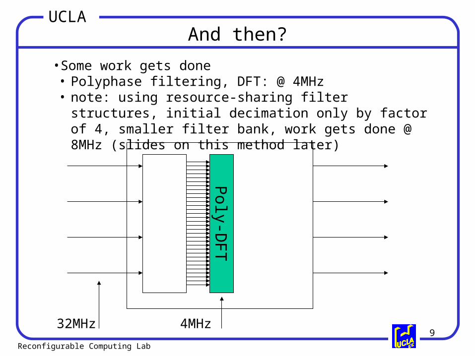
UCLAAnd then?
•Some work gets done• Polyphase filtering, DFT: @ 4MHz• note: using resource-sharing filter structures, initial decimation
only by factor of 4, smaller filter bank, work gets done @ 8MHz (slides on this method later)
32MHz 4MHz
Poly-D
FT
10Reconfigurable Computing Lab
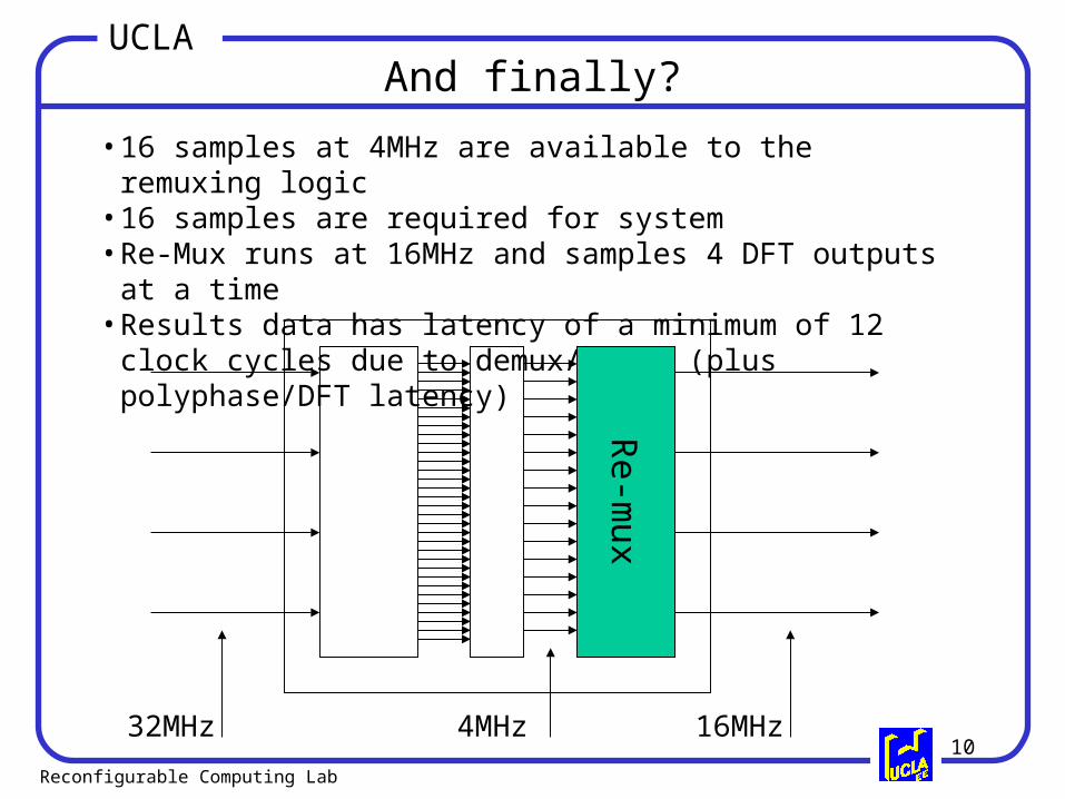
UCLAAnd finally?
• 16 samples at 4MHz are available to the remuxing logic• 16 samples are required for system• Re-Mux runs at 16MHz and samples 4 DFT outputs at a time• Results data has latency of a minimum of 12 clock cycles due to
demux/remux (plus polyphase/DFT latency)
32MHz 4MHz
Re-m
ux
16MHz

11Reconfigurable Computing Lab
UCLAPolyphase Filter Banks
The following slides describe the regular polyphase filter bank, the transpose form FIR filter, and optimizations based on symmetry
This is a symmetric FIR filter, i.e., the first n/2 and the last n/2 coeffs are the same, albeit in reverse order.
We can exploit this symmetry to implement an optimal form of the filter bank, using resource sharing.
We also describe two methods of exploiting resource sharing. The advantage of these schemes is the reduction in the size of both the filter bank and the commutator.

12Reconfigurable Computing Lab
UCLAThe Polyphase Filter bank Design
• First step is to design a prototype low-pass, FIR filter h(n) with the desired filter parameters
• The I polyphase filters pk , each of integer length K = M/I are derived from the length M FIR filter h(n) via
• pk(n) = h(k + nI), k = 0..I-1, n = 0..K-1
• (M is selected to be a multiple of I)
13Reconfigurable Computing Lab
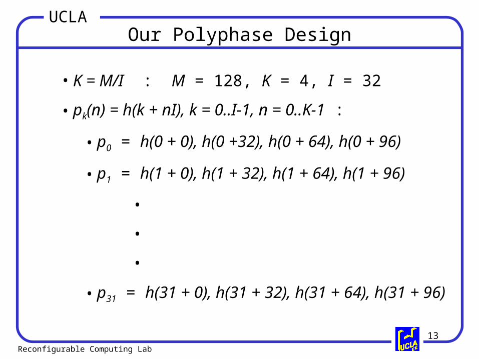
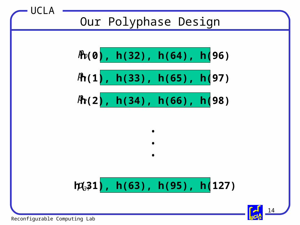
UCLAOur Polyphase Design
• K = M/I : M = 128, K = 4, I = 32
• pk(n) = h(k + nI), k = 0..I-1, n = 0..K-1 :
• p0 = h(0 + 0), h(0 +32), h(0 + 64), h(0 + 96)
• p1 = h(1 + 0), h(1 + 32), h(1 + 64), h(1 + 96)
•
•
•
• p31 = h(31 + 0), h(31 + 32), h(31 + 64), h(31 + 96)
14Reconfigurable Computing Lab
UCLAOur Polyphase Design
h(0), h(32), h(64), h(96)
h(1), h(33), h(65), h(97)
h(2), h(34), h(66), h(98)
h(31), h(63), h(95), h(127)
p0
• • •
p1
p2
p31
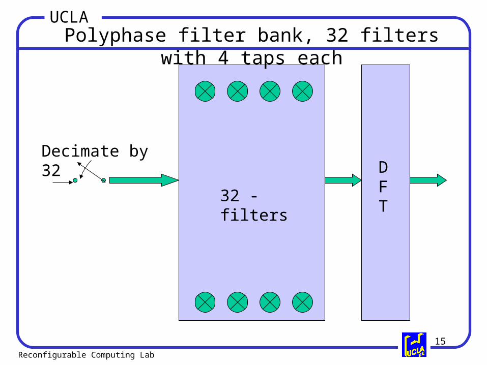
15Reconfigurable Computing Lab
UCLA
32 - filters
DFT
Polyphase filter bank, 32 filters with 4 taps each
Decimate by 32
16Reconfigurable Computing Lab
UCLA
Symmetry - how is it useful?
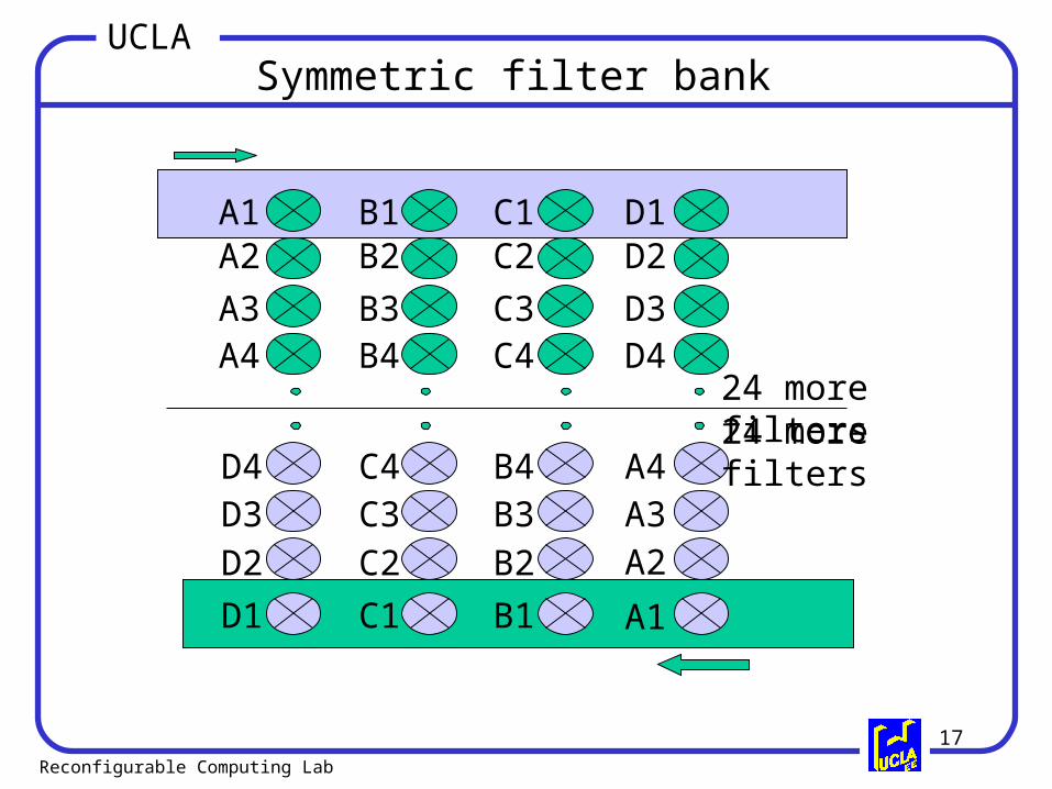
17Reconfigurable Computing Lab
UCLASymmetric filter bank
A1
D1
D2
D3D4
A4A3
A2B1
C1
C2
C3C4
B4B3
B2C1
B1
B2
B3B4
C4C3
C2D1
A1
A2A3A4
D4D3
D2
24 more filters24 more filters
18Reconfigurable Computing Lab
UCLASymmetry - how is it useful?
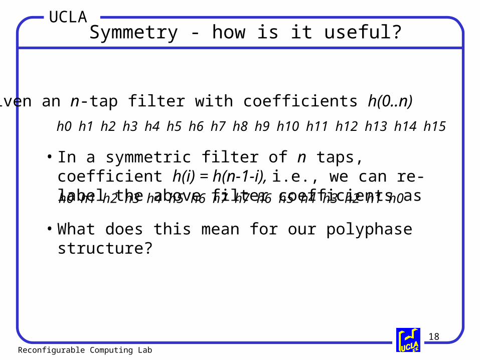
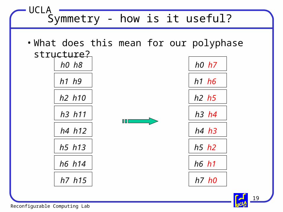
• Given an n-tap filter with coefficients h(0..n)
h0 h1 h2 h3 h4 h5 h6 h7 h8 h9 h10 h11 h12 h13 h14 h15
• In a symmetric filter of n taps, coefficient h(i) = h(n-1-i), i.e., we can re-label the above filter coefficients as
h0 h1 h2 h3 h4 h5 h6 h7 h7 h6 h5 h4 h3 h2 h1 h0
• What does this mean for our polyphase structure?
19Reconfigurable Computing Lab
UCLASymmetry - how is it useful?
h0 h8
• What does this mean for our polyphase structure?
h1 h9
h2 h10
h3 h11
h4 h12
h5 h13
h6 h14
h7 h15
h0 h7
h1 h6
h2 h5
h3 h4
h4 h3
h5 h2
h6 h1
h7 h0
20Reconfigurable Computing Lab
UCLASymmetry - how is it useful?
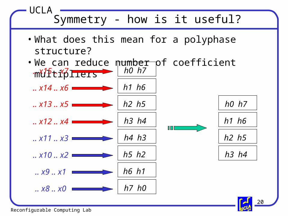
• What does this mean for a polyphase structure?• We can reduce number of coefficient multipliers
h0 h7
h1 h6
h2 h5
h3 h4
h4 h3
h5 h2
h6 h1
h7 h0 .. x8 .. x0
.. x9 .. x1
.. x10 .. x2
.. x11 .. x3
.. x12 .. x4
.. x13 .. x5
.. x14 .. x6
.. x15 .. x7
h0 h7
h1 h6
h2 h5
h3 h4
21Reconfigurable Computing Lab
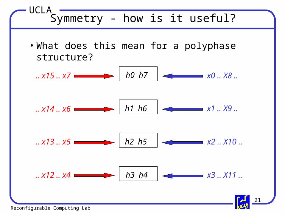
UCLASymmetry - how is it useful?
• What does this mean for a polyphase structure?
x0 .. X8 ..
x1 .. X9 ..
x2 .. X10 ..
x3 .. X11 .... x12 .. x4
.. x13 .. x5
.. x14 .. x6
.. x15 .. x7 h0 h7
h1 h6
h2 h5
h3 h4
22Reconfigurable Computing Lab
UCLA
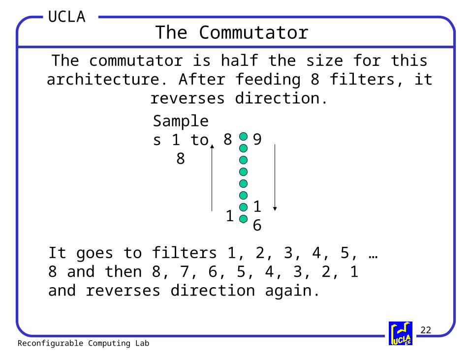
The commutator is half the size for this architecture. After feeding 8 filters, it reverses direction.
The Commutator
8
1 16
9
It goes to filters 1, 2, 3, 4, 5, … 8 and then 8, 7, 6, 5, 4, 3, 2, 1 and reverses direction again.
Samples 1 to 8

23Reconfigurable Computing Lab
UCLASymmetry - how is it useful?
Hardware Implementation

24Reconfigurable Computing Lab
UCLATranspose Form of the FIR filter
h0 h1 h2 h3
x(n)
y(n)
register adder multiplier

25Reconfigurable Computing Lab
UCLAResource Sharing Optimization - Scheme 1
h0 h1 h2 h3
x(n)
Clocked for even samples
Clocked for odd samples
Convolution of even samples
Convolution of odd samples
y(n)
y(n)
26Reconfigurable Computing Lab
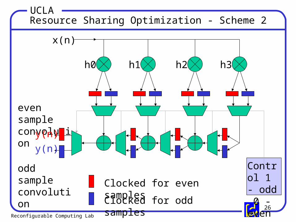
UCLA
h0 h1 h2 h3
x(n)
Control 1 - odd 0 - even
even sample convolution
odd sample convolution Clocked for even samples
Clocked for odd samples
y(n)
y(n)
Resource Sharing Optimization - Scheme 2
27Reconfigurable Computing Lab
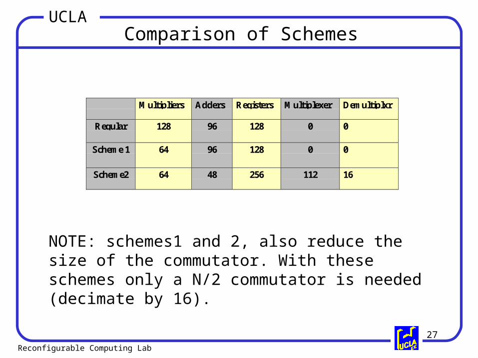
UCLA
Multipliers Adders Registers Multiplexer Demultiplxr
Regular 128 96 128 0 0
Scheme 1 64 96 128 0 0
Scheme2 64 48 256 112 16
Comparison of Schemes
NOTE: schemes1 and 2, also reduce the size of the commutator. With these schemes only a N/2 commutator is needed (decimate by 16).
28Reconfigurable Computing Lab
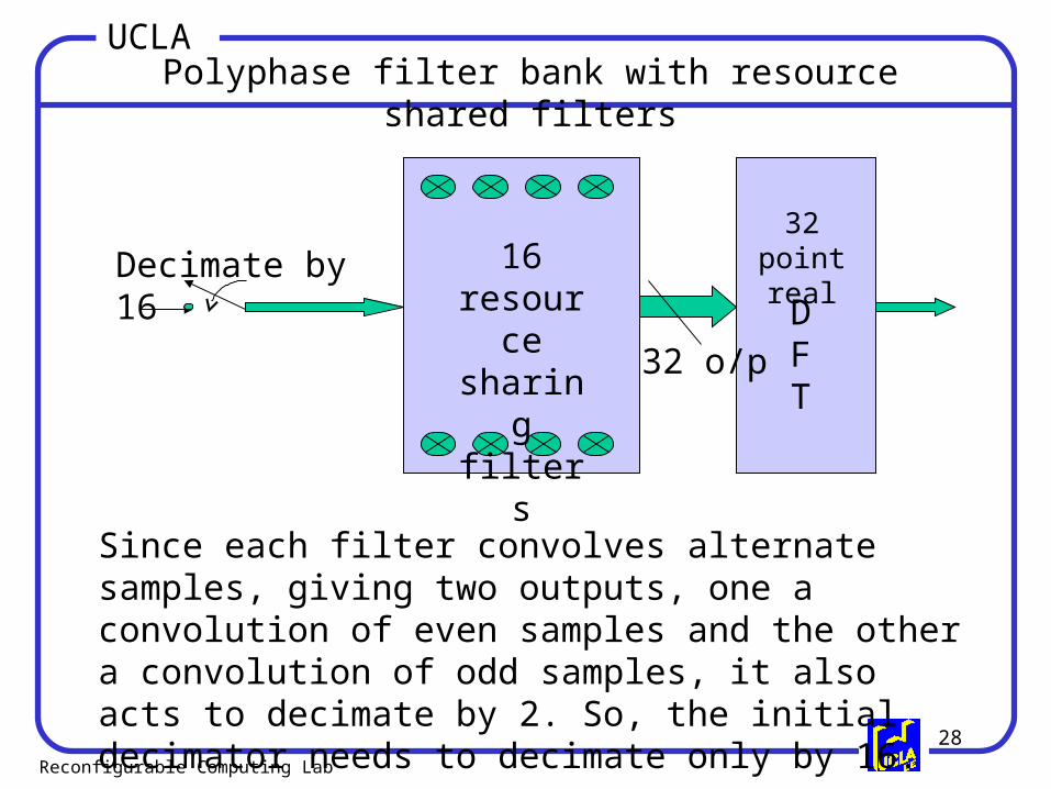
UCLAPolyphase filter bank with resource shared filters
Decimate by 16 16 resource sharing filters
32 o/p
32 point real
DFT
Since each filter convolves alternate samples, giving two outputs, one a convolution of even samples and the other a convolution of odd samples, it also acts to decimate by 2. So, the initial decimator needs to decimate only by 16.

29Reconfigurable Computing Lab
UCLA
The commutator is half the size for this architecture. After feeding 16 filters, it reverses direction.
The Commutator
16
1 32
17
It goes to filters 1, 2, 3, 4, 5, … 16 and then 16... 6, 5, 4, 3, 2, 1 and reverses direction again.
Samples 1 to 16
30Reconfigurable Computing Lab
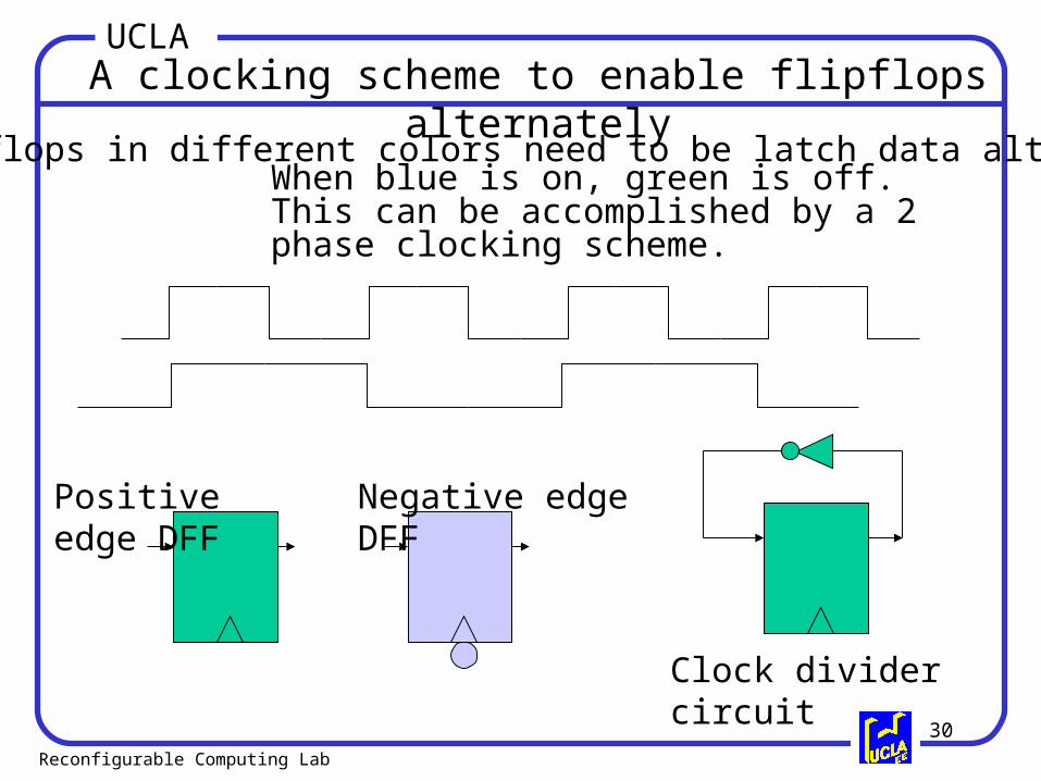
UCLA
Positive edge DFF Negative edge DFF
Clock divider circuit
A clocking scheme to enable flipflops alternately
The flipflops in different colors need to be latch data alternately.When blue is on, green is off. This can be accomplished by a 2 phase clocking scheme.

31Reconfigurable Computing Lab
UCLAAlternate scheme using enable flipflops
Clock enable
Instead of positive and negative DFFs, enable FFs can be used to convolve alternate samples. This clock enable also can be used as the select line to the muxes and demuxes.

32Reconfigurable Computing Lab
UCLAInitial Studies
The initial work involved approaching the topic from a theoretical standpoint
• understand polyphase theory
• implement polyphase structure simulation
• DSP Canvas
• MatLab
• create filter based on design specs from Fiore’s paper
• generate initial size estimates based on knowledge of the size of components and number of CLB’s necessary to implement them on an FPGA

33Reconfigurable Computing Lab
UCLAFeasibility Experiments
These experiments evaluated the feasibility of implementing the polyphase filter bank on an Altera Flex10K250A (part EPF10K250AGC599-1) a Xilinx XC40150 (part XC40150XV-09-BG560) and a Xilinx VirtexXCV1000 (part XCV1000-4-BG560)
All experiments were synthesized using Synplify 5.1.4 and placed and routed with Maxplus2 9.1
The filter bank consisted of a decimator at the input, feeding a bank of either 16 or 32, 4 tap filters (filters optimized for symmetry have 2 outputs). The outputs of the filter bank feed a commutator that “re-muxes” data onto 4 lines that will feed a DFT (assumption that the DFT is on another chip).

34Reconfigurable Computing Lab
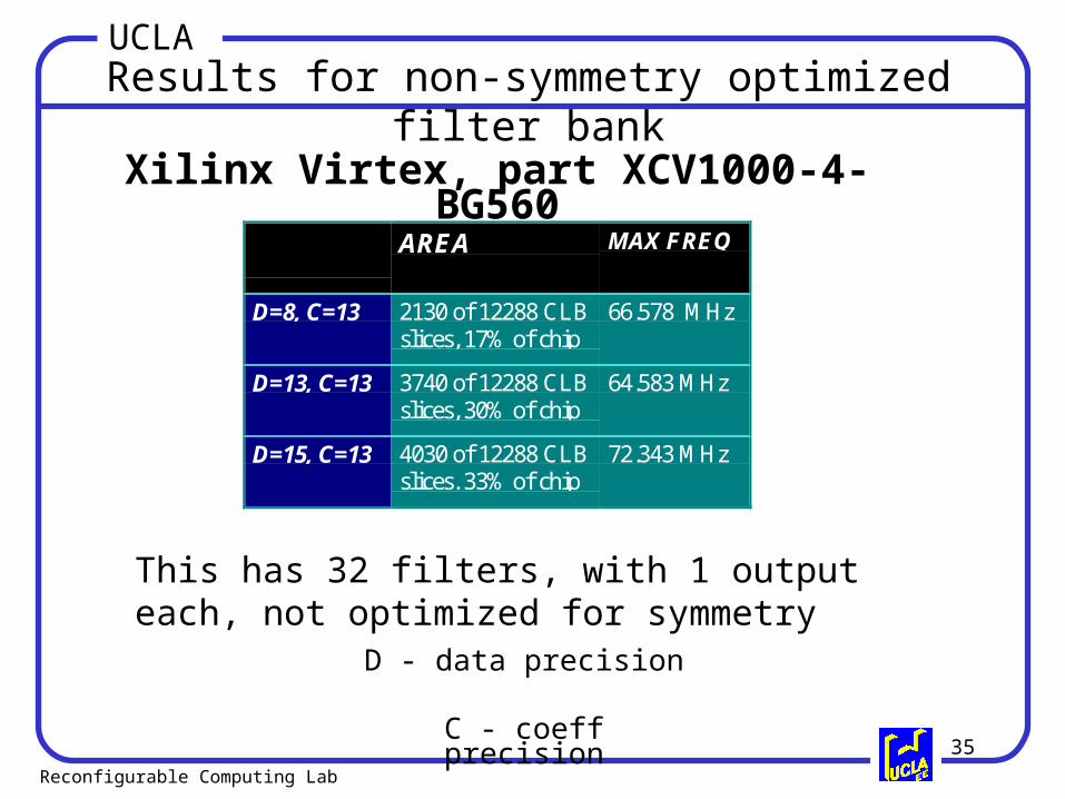
UCLAResults for non-symmetry optimized filter bank
Flex10K250A, part EPF10k250AGC599-1, does not fit.
The critical resource on an Altera Flex10K is the carry chain (fast interconnect) routing.
32 filters, with 1 output each, not optimized for symmetry
35Reconfigurable Computing Lab
UCLAResults for non-symmetry optimized filter bank
AREA MAX FREQ
D=8, C=13 2130 of 12288 CLBslices, 17% of chip
66.578 MHz
D=13, C=13 3740 of 12288 CLBslices, 30% of chip
64.583 MHz
D=15, C=13 4030 of 12288 CLBslices. 33% of chip
72.343 MHz
Xilinx Virtex, part XCV1000-4-BG560
This has 32 filters, with 1 output each, not optimized for symmetry
D - data precision
C - coeff precision
36Reconfigurable Computing Lab
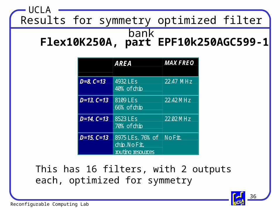
UCLA
AREA MAX FREQ
D=8, C=13 4932 LEs40% of chip
22.47 MHz
D=13, C=13 8109 LEs66% of chip
22.42 MHz
D=14, C=13 8523 LEs70% of chip
22.02 MHz
D=15, C=13 8975 LEs. 76% ofchip. No Fit,routing resources
No Fit.
Results for symmetry optimized filter bank
Flex10K250A, part EPF10k250AGC599-1
This has 16 filters, with 2 outputs each, optimized for symmetry

37Reconfigurable Computing Lab
UCLAResults for symmetry optimized filter bank
Xilinx XC40150XV-09-BG560
This has 16 filters, with 2 outputs each, optimized for symmetry
AREA MAX FREQ
D=8, C=13 2946 of 5184 CLBslices, 56% of chip
31.448 MHz
38Reconfigurable Computing Lab
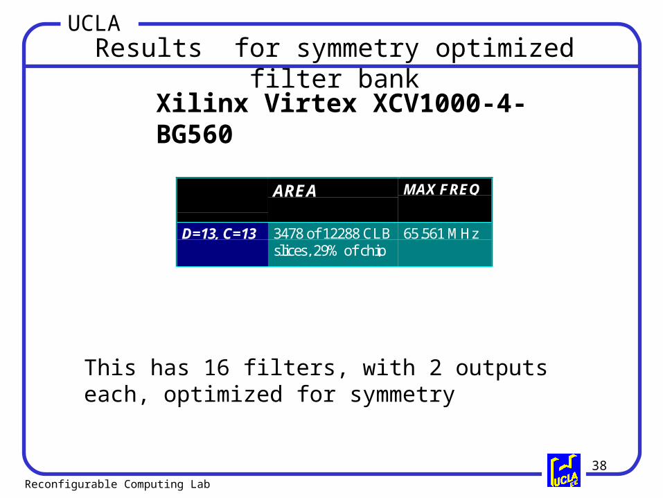
UCLAResults for symmetry optimized filter bank
Xilinx Virtex XCV1000-4-BG560
This has 16 filters, with 2 outputs each, optimized for symmetry
AREA MAX FREQ
D=13, C=13 3478 of 12288 CLBslices, 29% of chip
65.561 MHz

39Reconfigurable Computing Lab
UCLAFFT Implementation
The following slides describe some optimizations of the FFT and how its inclusion into the system logic affects size and speed.
• Goal of system is 16 distinct positive frequency bins
• An N-point FFT produces N/2+1 distinct bins
• Our input sequence is real
• The FFT of a real valued sequence of 2N points can be computed efficiently by employing an N-point complex FFT

40Reconfigurable Computing Lab
UCLA32-point Real FFT Implementation
X(n), the 2N point real sequence is divided into 2, N-point sequences as follows:
h(k) = x(2k), k = 0, 1, …., N - 1
g(k) = x(2k + 1), k = 0, 1, …., N - 1
i.e.. The function h(k) is equal to the even-numbered samples of x(k), and g(k) is equal to the odd-numbered samples.
A N-point complex valued sequence y(k) can be written as
y(k) = h(k) + j g(k)
The DFT of y(k) is then computed.
41Reconfigurable Computing Lab
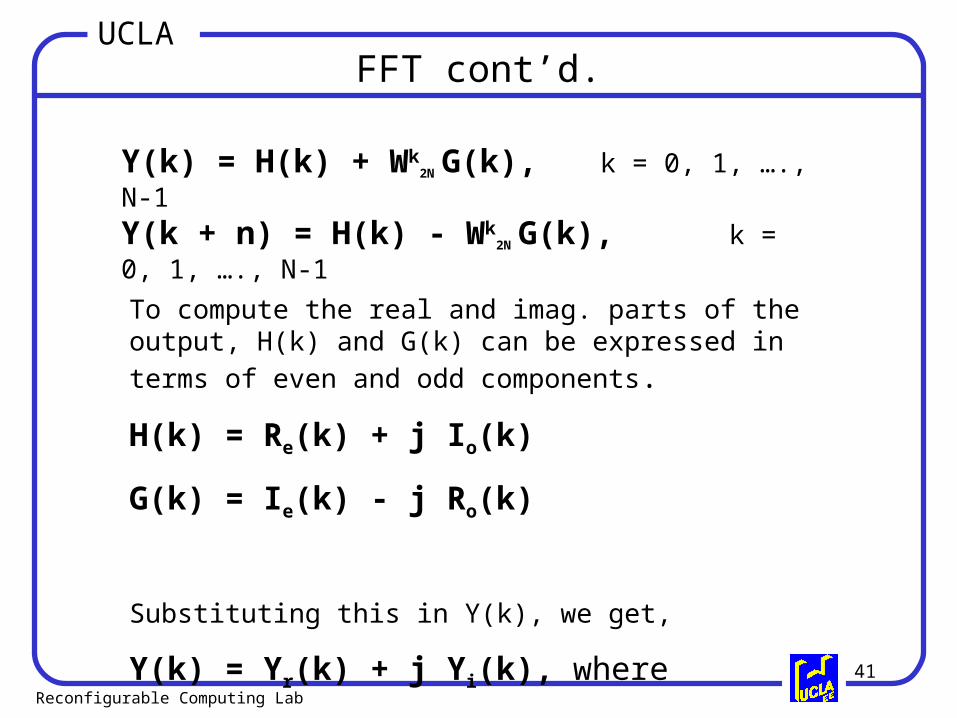
UCLAFFT cont’d.
Y(k) = H(k) + Wk2N G(k), k = 0, 1, …., N-1
Y(k + n) = H(k) - Wk2N G(k), k = 0, 1, …., N-1
To compute the real and imag. parts of the output, H(k) and G(k)
can be expressed in terms of even and odd components.
H(k) = Re(k) + j Io(k)
G(k) = Ie(k) - j Ro(k)
Substituting this in Y(k), we get,
Y(k) = Yr(k) + j Yi(k), where
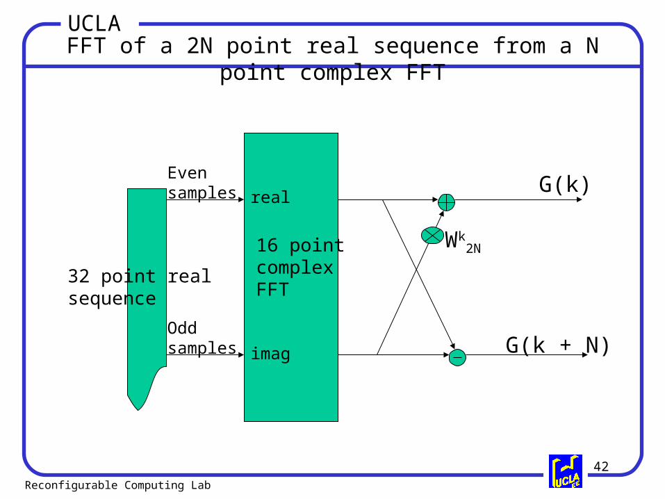
42Reconfigurable Computing Lab
UCLAFFT of a 2N point real sequence from a N point complex FFT
16 point complex FFT
real
imag
Even samples
Odd samples
Wk2N
G(k)
G(k + N)
32 point real sequence
43Reconfigurable Computing Lab
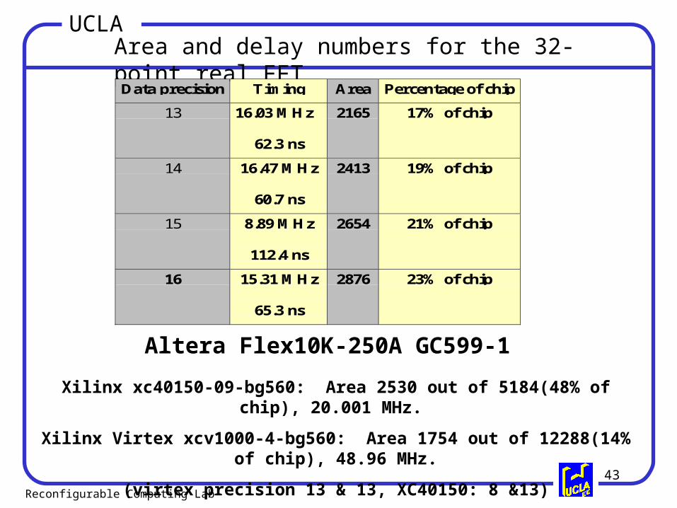
UCLAArea and delay numbers for the 32-point real FFT
Data precision Timing Area Percentage of chip
13 16.03 MHz
62.3 ns
2165 17% of chip
14 16.47 MHz
60.7 ns
2413 19% of chip
15 8.89 MHz
112.4 ns
2654 21% of chip
16 15.31 MHz
65.3 ns
2876 23% of chip
Altera Flex10K-250A GC599-1
Xilinx xc40150-09-bg560: Area 2530 out of 5184(48% of chip), 20.001 MHz.
Xilinx Virtex xcv1000-4-bg560: Area 1754 out of 12288(14% of chip), 48.96 MHz.
(virtex precision 13 & 13, XC40150: 8 &13)

44Reconfigurable Computing Lab
UCLAFull System Estimates
The entire polyphase filter bank along with the FFT does not fit on an Altera Flex device. But it does fit on the Xilinx XC40150 and Virtex.
Decimation factor = 32, 17 positive frequency bins
Data precision = 13, Coeff precision = 13
Xilinx xc40150-09-bg560 (D=8, C=13)4581 CLBs out of 5184 - 88% of chip.Freq: 20.492 MHz
Xilinx Virtex - xcv1000-4-bg5607156 CLB slices out of 12288 - 58% of chip.(11631 LUTs).Freq: 56.715 MHz.
45Reconfigurable Computing Lab
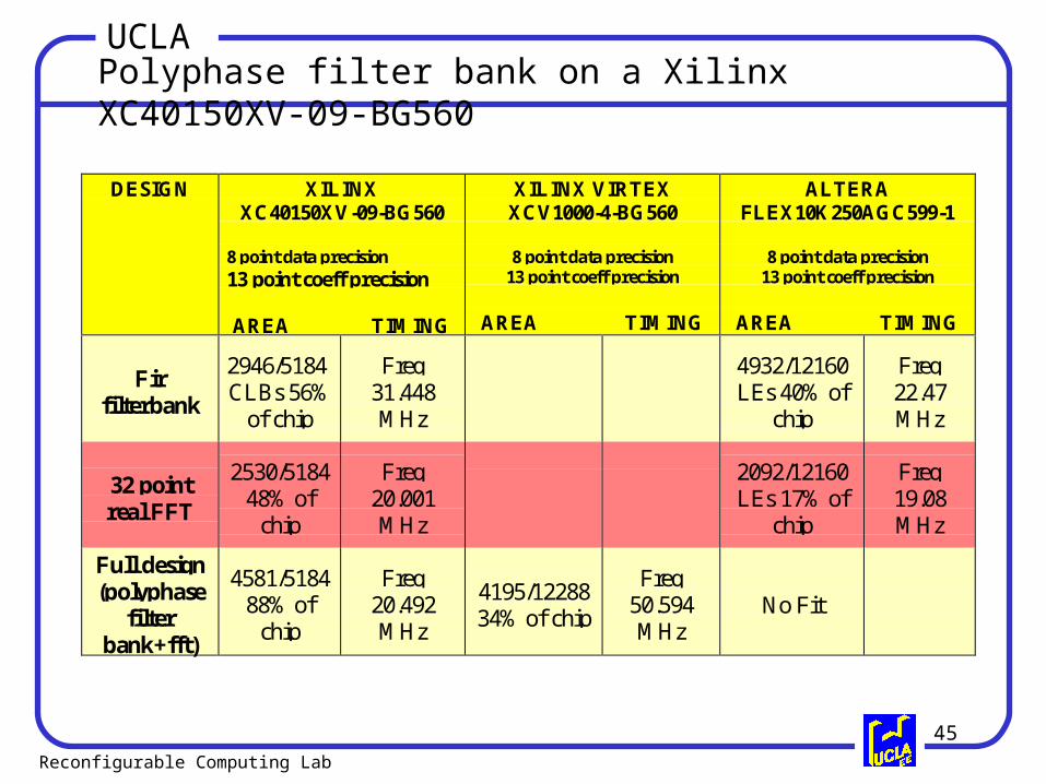
UCLAPolyphase filter bank on a Xilinx XC40150XV-09-BG560
DESIGN XILINXXC40150XV-09-BG560
8 point data precision13 point coeff precision
AREA TIMING
XILINX VIRTEXXCV1000-4-BG560
8 point data precision13 point coeff precision
AREA TIMING
ALTERAFLEX10K250AGC599-1
8 point data precision13 point coeff precision
AREA TIMING
Firfilterbank
2946/5184CLBs 56%
of chip
Freq31.448MHz
4932/12160LEs 40% of
chip
Freq22.47MHz
32 pointreal FFT
2530/518448% of
chip
Freq20.001MHz
2092/12160LEs 17% of
chip
Freq19.08MHz
Full design(polyphase
filterbank+fft)
4581/518488% of
chip
Freq20.492MHz
4195/1228834% of chip
Freq50.594MHz
No Fit

46Reconfigurable Computing Lab
UCLAArea and delay estimation flow
VHDL
Synthesis
Place & route
Timing analysis
RTL schematics
Area report
Timing report
Verify VHDL by checking the RTL level schematics, checking the number of adders, multipliers and registers.
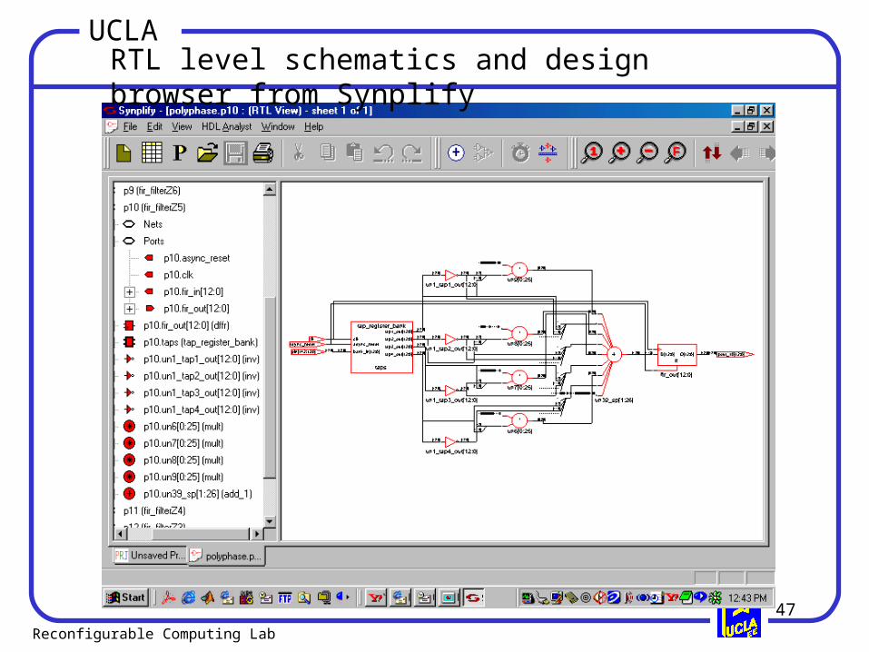
47Reconfigurable Computing Lab
UCLARTL level schematics and design browser from Synplify
48Reconfigurable Computing Lab
UCLAFuture Work
Simulate and test polyphase VHDL implementation using LANL test vectors
Work together with LANL to facilitate possible demo of polyphase work
Implement Scheme 2 of resource sharing symmetrical filter bank
Study the advantages and disadvantages with regards to system goals of FFT replacing the FFT with a DCT
Look into adaptive filtering techniques
Modifying our current polyphase design to accommodate configurable or even programmable rate
49Reconfigurable Computing Lab
UCLAConclusions
Very productive intitial phase of collaboration between UCLA and LANL
Our work has resulted in some innovations at the algorithmic level
Task migration from ASIC to FPGA
This study has provided useful sizing information for the Altera Flex and Xilinx Virtex families as well as some initial benchmarks of basic DSP methods used in UWB