


Languages
Pages
Legal

Application ReportSZZA043 - January 2004
1
Use of the CMOS Unbuffered Inverter in Oscillator Circuits
Moshiul Haque and Ernest Cox Standard Linear & Logic
ABSTRACT
CMOS devices have a high input impedance, high gain, and high bandwidth. Thesecharacteristics are similar to ideal amplifier characteristics and, hence, a CMOS buffer orinverter can be used in an oscillator circuit in conjunction with other passive components.Now, CMOS oscillator circuits are widely used in high-speed applications because they areeconomical, easy to use, and take significantly less space than a conventional oscillator.Among the CMOS devices, the unbuffered inverter (’U04) is widely used in oscillatorapplications. This application report discusses the performance of some TI ’U04 devices ina typical crystal-oscillator circuit.
Contents
1 Introduction 3. . . . . . . . . . . . . . . . . . . . . . . . . . . . . . . . . . . . . . . . . . . . . . . . . . . . . . . . . . . . . . . . . . . . . . . . . 2 Theory of Oscillators 3. . . . . . . . . . . . . . . . . . . . . . . . . . . . . . . . . . . . . . . . . . . . . . . . . . . . . . . . . . . . . . . . .
2.1 Characteristics of Crystals 3. . . . . . . . . . . . . . . . . . . . . . . . . . . . . . . . . . . . . . . . . . . . . . . . . . . . . . . . . 3 Buffered and Unbuffered CMOS Inverters in Oscillator Circuits 6. . . . . . . . . . . . . . . . . . . . . . . . . 4 Characteristics of a CMOS Unbuffered Inverter 7. . . . . . . . . . . . . . . . . . . . . . . . . . . . . . . . . . . . . . . .
4.1 Open-Loop Gain 7. . . . . . . . . . . . . . . . . . . . . . . . . . . . . . . . . . . . . . . . . . . . . . . . . . . . . . . . . . . . . . . . . 4.2 VO vs VI 8. . . . . . . . . . . . . . . . . . . . . . . . . . . . . . . . . . . . . . . . . . . . . . . . . . . . . . . . . . . . . . . . . . . . . . . . . 4.3 ICC vs VI 9. . . . . . . . . . . . . . . . . . . . . . . . . . . . . . . . . . . . . . . . . . . . . . . . . . . . . . . . . . . . . . . . . . . . . . . . 4.4 Variation of Duty Cycle With Temperature 10. . . . . . . . . . . . . . . . . . . . . . . . . . . . . . . . . . . . . . . . . . .
5 Characteristics of LVC1404 11. . . . . . . . . . . . . . . . . . . . . . . . . . . . . . . . . . . . . . . . . . . . . . . . . . . . . . . . . . 6 Practical Oscillator Circuits 12. . . . . . . . . . . . . . . . . . . . . . . . . . . . . . . . . . . . . . . . . . . . . . . . . . . . . . . . .
6.1 Selection of Resistors and Capacitors 13. . . . . . . . . . . . . . . . . . . . . . . . . . . . . . . . . . . . . . . . . . . . . . 6.1.1 RF 13. . . . . . . . . . . . . . . . . . . . . . . . . . . . . . . . . . . . . . . . . . . . . . . . . . . . . . . . . . . . . . . . . . . . . . 6.1.2 RS 13. . . . . . . . . . . . . . . . . . . . . . . . . . . . . . . . . . . . . . . . . . . . . . . . . . . . . . . . . . . . . . . . . . . . . . 6.1.3 C1 and C2 16. . . . . . . . . . . . . . . . . . . . . . . . . . . . . . . . . . . . . . . . . . . . . . . . . . . . . . . . . . . . . . .
7 Practical Design Tips 16. . . . . . . . . . . . . . . . . . . . . . . . . . . . . . . . . . . . . . . . . . . . . . . . . . . . . . . . . . . . . . . Appendix A. Laboratory Setup 18. . . . . . . . . . . . . . . . . . . . . . . . . . . . . . . . . . . . . . . . . . . . . . . . . . . . . . . . . . .
A.1 Laboratory Setup to Measure Open-Loop-Gain Characteristics 18. . . . . . . . . . . . . . . . . . . . . . . . A.2 Laboratory Setup to Measure ICC vs VI Characteristics 18. . . . . . . . . . . . . . . . . . . . . . . . . . . . . . .
Appendix B. LVC1GU04 in Crystal-Oscillator Applications 19. . . . . . . . . . . . . . . . . . . . . . . . . . . . . . . . . B.1 LVC1GU04 in 25-MHz Crystal-Oscillator Circuit 19. . . . . . . . . . . . . . . . . . . . . . . . . . . . . . . . . . . . . B.2 LVC1GU04 in 10-MHz Crystal-Oscillator Circuit 20. . . . . . . . . . . . . . . . . . . . . . . . . . . . . . . . . . . . . B.3 LVC1GU04 in 2-MHz Crystal-Oscillator Circuit 21. . . . . . . . . . . . . . . . . . . . . . . . . . . . . . . . . . . . . . . B.4 LVC1GU04 in 100-kHz Crystal-Oscillator Circuit 22. . . . . . . . . . . . . . . . . . . . . . . . . . . . . . . . . . . . .
Trademarks are the property of their respective owners.

SZZA043
2 Use of the CMOS Unbuffered Inverter in Oscillator Circuits
Appendix C. LVC1404 in Crystal-Oscillator Applications 23. . . . . . . . . . . . . . . . . . . . . . . . . . . . . . . . . . . C.1 LVC1404 in 25-MHz Crystal-Oscillator Circuit 23. . . . . . . . . . . . . . . . . . . . . . . . . . . . . . . . . . . . . . . C.2 LVC1404 in 100-kHz Crystal-Oscillator Circuit 24. . . . . . . . . . . . . . . . . . . . . . . . . . . . . . . . . . . . . . .
List of Figures
1 Oscillator 3. . . . . . . . . . . . . . . . . . . . . . . . . . . . . . . . . . . . . . . . . . . . . . . . . . . . . . . . . . . . . . . . . . . . . 2 Electrical-Equivalent Circuit of a Crystal 4. . . . . . . . . . . . . . . . . . . . . . . . . . . . . . . . . . . . . . . . . . 3 Pierce Oscillator Using CMOS Inverter 5. . . . . . . . . . . . . . . . . . . . . . . . . . . . . . . . . . . . . . . . . . . 4 Open-Loop-Gain Characteristics of LVC1GU04 6. . . . . . . . . . . . . . . . . . . . . . . . . . . . . . . . . . . . 5 Open-Loop-Gain Characteristics of AHC1GU04 6. . . . . . . . . . . . . . . . . . . . . . . . . . . . . . . . . . . 6 Open-Loop-Gain Characteristics of AUC1GU04 7. . . . . . . . . . . . . . . . . . . . . . . . . . . . . . . . . . . 7 VO vs VI Characteristics of LVC1GU04 7. . . . . . . . . . . . . . . . . . . . . . . . . . . . . . . . . . . . . . . . . . . 8 VO vs VI characteristics of AHC1GU04 8. . . . . . . . . . . . . . . . . . . . . . . . . . . . . . . . . . . . . . . . . . . 9 VO vs VI Characteristics of AUC1GU04 8. . . . . . . . . . . . . . . . . . . . . . . . . . . . . . . . . . . . . . . . . . . 10 ICC vs VI Characteristics of LVC1GU04 8. . . . . . . . . . . . . . . . . . . . . . . . . . . . . . . . . . . . . . . . . . . 11 ICC vs VI Characteristics of AHC1GU04 10. . . . . . . . . . . . . . . . . . . . . . . . . . . . . . . . . . . . . . . . . 12 ICC vs VI Characteristics of AUC1GU04 10. . . . . . . . . . . . . . . . . . . . . . . . . . . . . . . . . . . . . . . . . 13 Duty-Cycle Variation in LVC1GU04 10. . . . . . . . . . . . . . . . . . . . . . . . . . . . . . . . . . . . . . . . . . . . . . 14 Duty-Cycle Variation in AHC1GU04 11. . . . . . . . . . . . . . . . . . . . . . . . . . . . . . . . . . . . . . . . . . . . . 15 Duty−Cycle Variation in AUC1GU04 11. . . . . . . . . . . . . . . . . . . . . . . . . . . . . . . . . . . . . . . . . . . . . 16 Pinout Diagram for LVC1404 11. . . . . . . . . . . . . . . . . . . . . . . . . . . . . . . . . . . . . . . . . . . . . . . . . . . 17 Logic Diagram of LVC1404 12. . . . . . . . . . . . . . . . . . . . . . . . . . . . . . . . . . . . . . . . . . . . . . . . . . . . . 18 Open-Loop-Gain Characteristics of LVC1404 12. . . . . . . . . . . . . . . . . . . . . . . . . . . . . . . . . . . . . 19 Pierce Oscillator Circuit Using Unbuffered CMOS Inverter 13. . . . . . . . . . . . . . . . . . . . . . . . . . 20 Effect of RS on Oscillator Waveform (No Load) 14. . . . . . . . . . . . . . . . . . . . . . . . . . . . . . . . . . . 21 Effect of RS on Oscillator Waveform (RL = 1 k) 14. . . . . . . . . . . . . . . . . . . . . . . . . . . . . . . . . . 22 Effect of RS on the Frequency Response of Feedback Network 15. . . . . . . . . . . . . . . . . . . . . 23 Effect of RS on the Phase Response of Feedback Network 15. . . . . . . . . . . . . . . . . . . . . . . . . 24 Oscillator Circuit Using a Schmitt-Trigger Input Inverter 17. . . . . . . . . . . . . . . . . . . . . . . . . . . . A-1 Open-Loop-Gain Measurement Setup 18. . . . . . . . . . . . . . . . . . . . . . . . . . . . . . . . . . . . . . . . . . . A-2 ICC vs VI Measurement Setup 18. . . . . . . . . . . . . . . . . . . . . . . . . . . . . . . . . . . . . . . . . . . . . . . . . . B-1 Effect of RS on Duty Cycle and ICC (Frequency = 25 MHz) 19. . . . . . . . . . . . . . . . . . . . . . . . . B-2 Effect of RS on Duty Cycle and ICC (Frequency = 10 MHz) 20. . . . . . . . . . . . . . . . . . . . . . . . . B-3 Effect of RS on Duty Cycle and ICC (Frequency = 2 MHz) 21. . . . . . . . . . . . . . . . . . . . . . . . . . B-4 Effect of RS on Duty Cycle and ICC (Frequency = 100 kHz) 22. . . . . . . . . . . . . . . . . . . . . . . . C-1 Output Waveform of Oscillator Circuit Using LVC1404 (Frequency = 25 MHz) 23. . . . . . . . . C-2 Output Waveform of Oscillator Circuit Using LVC1404 (Frequency = 100 kHz) 24. . . . . . . .
List of Tables
B-1 Effect of RS on Duty Cycle and ICC (Frequency = 25 MHz) 19. . . . . . . . . . . . . . . . . . . . . . . . . B-2 Effect of RS on Duty Cycle and ICC (Frequency = 10 MHz) 20. . . . . . . . . . . . . . . . . . . . . . . . . B-3 Effect of RS on Duty Cycle and ICC (Frequency = 2 MHz) 21. . . . . . . . . . . . . . . . . . . . . . . . . . B-4 Effect of RS on Duty Cycle and ICC (Frequency = 100 kHz) 22. . . . . . . . . . . . . . . . . . . . . . . .

SZZA043
3 Use of the CMOS Unbuffered Inverter in Oscillator Circuits
1 Introduction
Resistors, inductors, capacitors, and an amplifier with high gain are the basic components of anoscillator. In designing oscillators, instead of using discrete passive components (resistors,inductors, and capacitors), crystal oscillators are a better choice because of their excellentfrequency stability and wide frequency range. A crystal basically is an RLC network that has anatural frequency of resonance.
2 Theory of Oscillators
In principle, an oscillator can be composed of an amplifier, A, with voltage gain, a, and phaseshift, α, and a feedback network, F, with transfer function, f, and phase shift, β (see Figure 1).
V1 V2Amplifier, Aa,
Feedback Network, Ff,
Figure 1. Oscillator
For |f| || 1 the oscillating condition is fulfilled, and the system works as an oscillator.
f and a are complex quantities; consequently, it is possible to derive from equation 1
|f| || expj 1
the amplitude
|f| || 1
and the phase
2
To oscillate, these conditions of amplitude and phase must be met. These conditions are knownas the Barkhausen criterion. The closed-loop gain should be ≥1, and the total phase shift of 360degrees is to be provided.
2.1 Characteristics of Crystals
Figure 2 is an electrical-equivalent circuit of a quartz crystal.
(1)
(2)
(3)

SZZA043
4 Use of the CMOS Unbuffered Inverter in Oscillator Circuits
C0
RLC
Figure 2. Electrical-Equivalent Circuit of a Crystal
The quantities C and L are determined by the mechanical characteristics of the crystal; R is theresistance of the resonant circuit at the series resonance, and Co represents the capacitance ofthe leads and electrodes. Co is much larger than C and is affected by the stray capacitances ofthe final circuit. Because R is negligible, the impedance of this circuit is given by equation 4.
Z j 2LC 1
(Co C) 2LCCo
A series-resonance frequency is attained when the impedance, Z, approaches 0, Z → 0
LCfser
2
1=
A parallel-resonance frequency is attained when the impedance, Z, approaches ∞ , Z → ∞
oserpar C
Cff = 1 +
An oscillator circuit using the parallel resonance mode of the crystal is less stable than theequivalent circuit using the series resonance, because of the dependence on the external circuitparameter. For series resonance, the crystal appears as a series-resonant resistance, R. Forparallel resonance, the crystal appears as an inductive load.
In the oscillator circuit, the crystal acts as the feedback network. For proper operation, the inputimpedance of the amplifier should be well matched to the low series-resonant resistance of thecrystal. For HCMOS devices, because of the high input impedance, a crystal operated in seriesresonance would be completely mismatched. The solution is to operate the crystal inparallel-resonance mode. But, parallel resonance has a poor frequency response compared toseries resonance because of the dependence on Co (stray capacitance or circuit capacitance).Connecting a capacitance in parallel (CP) with the crystal can reduce the influence of Co on theparallel-resonance frequency. From the equation of the parallel-resonance frequency
oppar CC
C
LCf += 1 +
2
1
(4)
(5)
(6)
(7)
SZZA043
5 Use of the CMOS Unbuffered Inverter in Oscillator Circuits
By choosing CP > Co (Co is approximately 3 pF to 5 pF, and CP typically is 30 pF).
CP >> C (C is in the range of femtofarads)
LCf par
2
1≈
Now, the parallel-resonance frequency is approximately equal to the series-resonancefrequency.
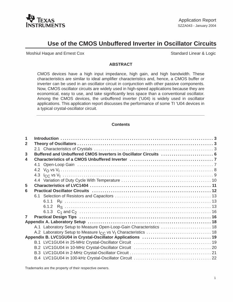
A popular application of the parallel-resonance circuit is the Pierce oscillator circuit (seeFigure 3) in which the parallel combination of C1 and C2 constitutes CP.
21
21
+ CC
CCCP =
C1 and C2 form a capacitor voltage divider that determines the degree of feedback. Thefeedback factor is given by
f C1
C2
RF
CMOS Inverter
Crystal C2C1
Figure 3. Pierce Oscillator Using CMOS Inverter
The optimal value for Cp determines the quality and frequency stability of the crystal oscillator.Usually, the crystal manufacturer’s data sheet specifies the recommended load for the crystal(CL). Cp represents the load for the crystal, and this should be equal to CL, as specified in thecrystal manufacturer’s data sheet.
In an oscillator circuit, the CMOS inverter operates in the linear mode and works as an amplifier.The phase shift provided by the inverter is 180 degrees. To meet the oscillating condition, thecrystal oscillator must provide an additional 180 degrees of phase shift. If C1 = C2, currentthrough them is identical and 180 degrees out of phase from each other. Hence, for C1 = C2, thecrystal provides a phase shift of 180 degrees.
The feedback resistor modifies the input impedance of the CMOS inverter. For an inverter withan open-loop gain much higher than 1, the input impedance becomes
(8)
(9)
(10)

SZZA043
6 Use of the CMOS Unbuffered Inverter in Oscillator Circuits
Zi RF
The parallel-resonance resistance of the crystal is modified by the load capacitor, Cp.
22 )(C
1
po
p+ CR
R =
Rp should match the input impedance of the CMOS inverter. For example, if a crystal oscillatorhas the following parameters:
Cp = CL = 30 pF
Co = 7 pF
R = 80 Ω at 5 MHz
Rp 1
80 2 5 1062 30 1012 7 10122From the calculation
Rp 10 k
Rp should be equal to Zi, i.e.,
Zi Rp 10 k
Zi RF 10 k
a
RZ F
i == 10 kΩ
RF 10 k
For a CMOS inverter with an open-loop gain, a = 100, the value of the feedback resistor iscalculated as:
RF 10000 100 1 106 1 M
By using a feedback resistor of 1 M, successful oscillation can be accomplished. In practicalapplications, the value of the feedback resistor usually will be greater than 1 M in order toattain higher input impedance, so the crystal can easily drive the inverter.
3 Buffered and Unbuffered CMOS Inverters in Oscillator CircuitsUnbuffered inverters have a single inverting stage, and the gain of this type of inverter is in therange of hundreds. Buffered inverters have more than one stage, and the gain is in the range ofseveral thousand. In the buffered inverter, power consumption usually is less than in theunbuffered inverter, because the first and the second inverter stages consume significantly lesspower-supply current than the output stage. Because the first stage remains in linear modeduring oscillation, a buffered inverter consumes less power than an unbuffered inverter. Bothbuffered and unbuffered inverters can be used for oscillator applications, with only slight designchanges. Because the gain of buffered inverters is very high, they are sensitive to parameterchanges in the oscillator circuit and are less stable than unbuffered inverters.
(11)
(12)
(13)
(14)
SZZA043
7 Use of the CMOS Unbuffered Inverter in Oscillator Circuits
4 Characteristics of a CMOS Unbuffered Inverter
The choice of a CMOS inverter for oscillator applications depends on various factors, forexample open-loop gain, power consumption, duty-cycle variation with temperature, etc. In thefollowing paragraphs, some of these characteristics of TI CMOS inverters that are critical inselecting an inverter for oscillator application are described.
4.1 Open-Loop Gain
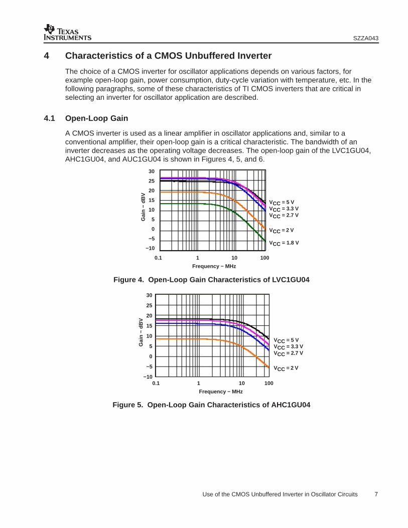
A CMOS inverter is used as a linear amplifier in oscillator applications and, similar to aconventional amplifier, their open-loop gain is a critical characteristic. The bandwidth of aninverter decreases as the operating voltage decreases. The open-loop gain of the LVC1GU04,AHC1GU04, and AUC1GU04 is shown in Figures 4, 5, and 6.
Frequency − MHz
VCC = 1.8 V
Gai
n −
dBV
0.1
VCC = 5 VVCC = 3.3 V
VCC = 2 V
1 10 100
30
25
20
15
10
5
0
−5
−10
VCC = 2.7 V
Figure 4. Open-Loop Gain Characteristics of LVC1GU04
Frequency − MHz
Gai
n −
dBV
0.1
VCC = 5 VVCC = 3.3 V
VCC = 2 V
1 10 100
30
25
20
15
10
5
0
−5
−10
VCC = 2.7 V
Figure 5. Open-Loop Gain Characteristics of AHC1GU04
SZZA043
8 Use of the CMOS Unbuffered Inverter in Oscillator Circuits
Frequency − MHz
Gai
n −
dBV
0.1
VCC = 2.5 V
VCC = 1 V
VCC = 2 V
1 10 100
30
25
20
15
10
5
0
−5
−10
VCC = 1.5 V
VCC = 0.8 V
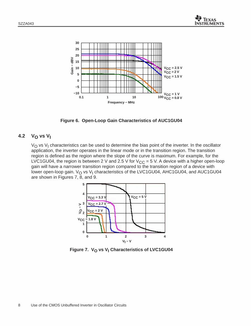
Figure 6. Open-Loop Gain Characteristics of AUC1GU04
4.2 VO vs VI
VO vs VI characteristics can be used to determine the bias point of the inverter. In the oscillatorapplication, the inverter operates in the linear mode or in the transition region. The transitionregion is defined as the region where the slope of the curve is maximum. For example, for theLVC1GU04, the region is between 2 V and 2.5 V for VCC = 5 V. A device with a higher open-loopgain will have a narrower transition region compared to the transition region of a device withlower open-loop gain. VO vs VI characteristics of the LVC1GU04, AHC1GU04, and AUC1GU04are shown in Figures 7, 8, and 9.
VCC = 5 V
VCC = 2 V
VCC = 3.3 V
1
5
VCC = 2.7 V
4
3
2
1
00 432
VI − V
VO
− V
VCC = 1.8 V
Figure 7. V O vs VI Characteristics of LVC1GU04

SZZA043
9 Use of the CMOS Unbuffered Inverter in Oscillator Circuits
1
5
4
3
2
1
00 432
VI − VV
O −
V
VCC = 5 V
VCC = 3 V
VCC = 2.7 V
VCC = 2 V
Figure 8. V O vs VI Characteristics of AHC1GU04
VI − V
2.5
0
VCC = 1 V
2
1.5
1
0.5
00.5 1 1.5 2
VCC = 2.5 VVCC = 2 V
VCC = 1.5 V
VCC = 0.8 V
VO
− V
Figure 9. V O vs VI Characteristics of AUC1GU04
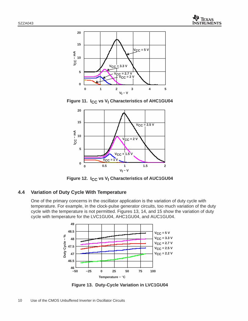
4.3 ICC vs VI
ICC vs VI characteristics of the LVC1GU04, AHC1GU04, and AUC1GU04 are shown in Figures10, 11, and 12. This characteristic determines the dynamic power consumption of the inverter inthe oscillator circuit. The setup is shown in Appendix A. Due to the 1-kΩ load, ICC is high whenVI is 0.
VI − V
70
0 41 32
VCC = 5 V
5
60
50
40
30
20
10
0
I CC
− m
A
VCC = 3.3 V
VCC = 2.7 V
VCC = 2 V
Figure 10. I CC vs VI Characteristics of LVC1GU04
SZZA043
10 Use of the CMOS Unbuffered Inverter in Oscillator Circuits
10
0
I CC
− m
A
15
5
20
VI − V0
VCC = 5 V
1 2 3 4 5
VCC = 3.3 V
VCC = 2.7 VVCC = 2 V
Figure 11. I CC vs VI Characteristics of AHC1GU04
20
10
0
I CC
− m
A
VI − V0 1.510.5
VCC = 2.5 V
2
15
5
VCC = 2 V
VCC = 1.5 V
VCC = 1 V
Figure 12. I CC vs VI Characteristics of AUC1GU04
4.4 Variation of Duty Cycle With Temperature
One of the primary concerns in the oscillator application is the variation of duty cycle withtemperature. For example, in the clock-pulse generator circuits, too much variation of the dutycycle with the temperature is not permitted. Figures 13, 14, and 15 show the variation of dutycycle with temperature for the LVC1GU04, AHC1GU04, and AUC1GU04.
49
Dut
y C
ycle
− %
Temperature − C
−50
VCC = 5 V48.5
48
47.5
47
46.5
46−25 50250 10075
VCC = 3.3 V
VCC = 2.7 V
VCC = 2.5 V
VCC = 2.2 V
Figure 13. Duty-Cycle Variation in LVC1GU04

SZZA043
11 Use of the CMOS Unbuffered Inverter in Oscillator Circuits
51
Dut
y C
ycle
− %
Temperature − C
−50
VCC = 5 V
50
49
48
47
46−25 50250 10075
VCC = 3.3 VVCC = 2.7 V
VCC = 2.5 VVCC = 2.2 V
Figure 14. Duty-Cycle Variation in AHC1GU04
47
Dut
y C
ycle
− %
Temperature − C−50
46.5
45.5
45
46
−25 50250 10075
VCC = 1.5 V
VCC = 1.2 V
VCC = 2.5 VVCC = 2.0 V
Figure 15. Duty-Cycle Variation in AUC1GU04
5 Characteristics of LVC1404
The TI LVC1404 is a dual inverter gate that is very suitable for oscillator applications. Thisdevice has a wide VCC range and can be used for a wide range of frequencies. The device hasboth unbuffered and buffered outputs. Figure 16 shows the pinout diagram and Figure 17shows the logic diagram for LVC1404.
1
2
3
4
8
7
6
5
CTRLXOUT
XINGND
VCCOSCOUTAY
Figure 16. Pinout Diagram for LVC1404
As shown in Figure 17, XIN is connected to an unbuffered inverter, and the output of this inverter(XOUT) is connected to the input of another inverter to get a clean rail-to-rail signal and toprovide sufficient drive capability. The crystal is connected between the XIN and XOUT.
SZZA043
12 Use of the CMOS Unbuffered Inverter in Oscillator Circuits
CTRL
XOUT
OSCOUT
1
2
7
Y6
XIN3
5A
Figure 17. Logic Diagram of LVC1404
Figure 18 shows the open-loop-gain characteristics of the unbuffered inverter of the LVC1404(i.e., between XIN and XOUT). The device provides a high gain over a wide range offrequencies.
30
Gai
n −
dBV
Frequency − MHz100
20
10
0
−101010.1
VCC = 1.8 V
VCC = 3.3 VVCC = 2.7 V
VCC = 5 V
Figure 18. Open-Loop-Gain Characteristics of LVC1404
6 Practical Oscillator Circuits
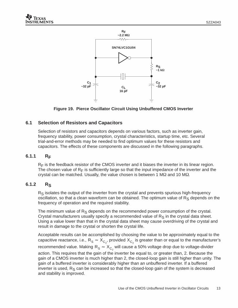
Figure 19 shows an example of an oscillator circuit that uses a 16-pF, 25-MHz crystal and anunbuffered inverter, LVC1GU04. In actual applications, the passive components may requireadjustment to get the desired oscillation. For example, C1 and C2 can be adjusted to take intoconsideration the input and output capacitance of the LVC1GU04 and the desired duty cycle ofoscillation.
Appendixes B and C show the performance of TI’s LVC1GU04 and LVC1404 devices in thisPierce crystal-oscillator circuit.
SZZA043
13 Use of the CMOS Unbuffered Inverter in Oscillator Circuits
CL16 pF
RF~2.2 M
SN74LVC1GU04
C2~32 pF
C1~32 pF
RS~1 k
Figure 19. Pierce Oscillator Circuit Using Unbuffered CMOS Inverter
6.1 Selection of Resistors and Capacitors
Selection of resistors and capacitors depends on various factors, such as inverter gain,frequency stability, power consumption, crystal characteristics, startup time, etc. Severaltrial-and-error methods may be needed to find optimum values for these resistors andcapacitors. The effects of these components are discussed in the following paragraphs.
6.1.1 RF
RF is the feedback resistor of the CMOS inverter and it biases the inverter in its linear region.The chosen value of RF is sufficiently large so that the input impedance of the inverter and thecrystal can be matched. Usually, the value chosen is between 1 M and 10 M.
6.1.2 RS
RS isolates the output of the inverter from the crystal and prevents spurious high-frequencyoscillation, so that a clean waveform can be obtained. The optimum value of RS depends on thefrequency of operation and the required stability.
The minimum value of RS depends on the recommended power consumption of the crystal.Crystal manufacturers usually specify a recommended value of RS in the crystal data sheet.Using a value lower than that in the crystal data sheet may cause overdriving of the crystal andresult in damage to the crystal or shorten the crystal life.
Acceptable results can be accomplished by choosing the value to be approximately equal to thecapacitive reactance, i.e., RS XC2
, provided XC2 is greater than or equal to the manufacturer’s
recommended value. Making RS XC2 will cause a 50% voltage drop due to voltage-divider
action. This requires that the gain of the inverter be equal to, or greater than, 2. Because thegain of a CMOS inverter is much higher than 2, the closed-loop gain is still higher than unity. Thegain of a buffered inverter is considerably higher than an unbuffered inverter. If a bufferedinverter is used, RS can be increased so that the closed-loop gain of the system is decreasedand stability is improved.

SZZA043
14 Use of the CMOS Unbuffered Inverter in Oscillator Circuits
The effect of RS is shown in Figures 20 and 21. Decreasing RS results in a faster edge rate andincreased closed-loop gain.
4
Out
put V
olta
ge −
V
Time − ns20
RS = 1 k (No Load)3.5
3
2.5
2
1.5
1
0.5
0
−0.540 60 80 100
RS = 3 k (No Load)
Figure 20. Effect of R S on Oscillator Waveform (No Load)
Time − ns
RS = 3 k (RL = 1 k
80 100
5
Out
put V
olta
ge −
V
20 40 60
4
3
2
1
0
−1
RS = 0 (RL = 1 k
Figure 21. Effect of R S on Oscillator Waveform (R L = 1 k)
Figures 22 and 23 show the relative effect of the RS on the gain and the phase response of thefeedback network of the oscillator circuit described in Figure 19. RS not only reduces the gain,but also shifts the resonance frequency and introduces additional phase delay.

SZZA043
15 Use of the CMOS Unbuffered Inverter in Oscillator Circuits
Frequency − MHz
RS = 240
5
Gai
n −d
B
24.98
0
−5
−10
−15
−20
−25
−30
24.99 25.00 25.01
RS = 3 k
Figure 22. Effect of R S on the Frequency Response of Feedback Network
Frequency − MHz
RS = 240
Pha
se −
Deg
24.98
0
−50
−100
−150
−200
−250
−30024.99 25.00 25.01
RS = 3 k
25.02
Figure 23. Effect of R S on the Phase Response of Feedback Network
RS also affects the duty cycle and power consumption (ICC) of the oscillator circuit. Appendix Bshows the effect of RS on duty cycle and the power consumption (ICC) in an oscillator circuitusing an LVC1GU04 as the amplifier.
At low frequency, phase shift due to the CMOS inverter is small and can be neglected. Phaseshift is given by equation 15.
Phase shift = Frequency of oscillation × Propagation delay × 360 degrees
If the propagation delay of a CMOS inverter is 5 ns, then, at 25 MHz, the phase shift introducedby the inverter is 45 degrees. For high frequency, using a series feedback resistor (RS) is notfeasible because it adds additional phase shift. RS can be replaced by a capacitor whose valueis approximately equal to the input impedance of the crystal, i.e., Cs ≈ C2.
(15)
SZZA043
16 Use of the CMOS Unbuffered Inverter in Oscillator Circuits
6.1.3 C1 and C2
The values of C1 and C2 are chosen such that the parallel combination of C1 and C2 equals therecommended capacitive load (CL) specified in the crystal data sheet, i.e.:
21
21
+ CC
CCCL
=
RS and C2 form a low-pass filter and reduce spurious oscillation. The value can be adjusted,based on the desired cutoff frequency. Another factor in choosing C2 is the start-up time. For alow-gain amplifier, sometimes C2 is increased over C1 to increase the phase-shift and help instart-up, but C1 should be within a limit such that the load capacitance introduced to the crystaldoes not exceed the manufacturer’s recommended value of CL. Otherwise, the resonancefrequency will change.
7 Practical Design Tips
The performance of an oscillator circuit using a CMOS inverter is sensitive to the circuitcomponents, layout etc. In designing an oscillator circuit, careful attention should be given toeliminate external effects:
• The oscillator circuit feedback factor should not be too large; otherwise, there will beinstability, and oscillation will not be determined by the crystal alone.
• A CMOS inverter with a Schmitt-trigger input is not suitable for use in the oscillator circuitdescribed previously. A Schmitt-trigger input device has two different thresholds, and it maynot be possible to bias them properly in the linear region using the circuit describedpreviously.
• At higher frequencies, the ground lead to the central point of connection always should be aslarge in area and as short in length as possible. This provides low resistance and lowinductance and, thereby, the effect on oscillation is less. Use of a multilayer board, with onelayer for VCC and one for ground, is preferable.
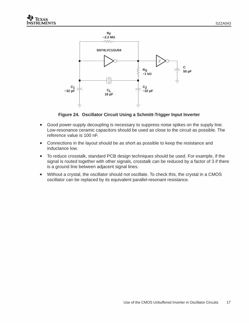
• An unbuffered inverter itself may not have enough drive for a high-capacitive load. As aresult, the output voltage swing may not be rail to rail. This also will slow down the edge rateof the output signal. To solve these problems, a buffer or inverter with a Schmitt-trigger inputcan be used at the output of the oscillator. Examples of Schmitt-trigger input buffers andinverters are the LVC1G17 and LVC1G14. Figure 24 shows an example circuit.
SZZA043
17 Use of the CMOS Unbuffered Inverter in Oscillator Circuits
RF~2.2 M
SN74LVC1GU04
CL16 pF
C2~32 pF
C1~32 pF
RS~1 k
C50 pF
Figure 24. Oscillator Circuit Using a Schmitt-Trigger Input Inverter
• Good power-supply decoupling is necessary to suppress noise spikes on the supply line.Low-resonance ceramic capacitors should be used as close to the circuit as possible. Thereference value is 100 nF.
• Connections in the layout should be as short as possible to keep the resistance andinductance low.
• To reduce crosstalk, standard PCB design techniques should be used. For example, if thesignal is routed together with other signals, crosstalk can be reduced by a factor of 3 if thereis a ground line between adjacent signal lines.
• Without a crystal, the oscillator should not oscillate. To check this, the crystal in a CMOSoscillator can be replaced by its equivalent parallel-resonant resistance.

SZZA043
18 Use of the CMOS Unbuffered Inverter in Oscillator Circuits
Appendix A. Laboratory Setup
A.1 Laboratory Setup to Measure Open-Loop Gain Characteristics2.2 M
’U04
1 k 30 pF50 50 mV
Peak-to-Peak ~
1 F
Figure A−1. Open-Loop-Gain Measurement Setup
A.2 Laboratory Setup to Measure I CC vs VI Characteristics2.2 M
’U04
1 k-+
Figure A−2. I CC vs VI Measurement Setup
SZZA043
19 Use of the CMOS Unbuffered Inverter in Oscillator Circuits
Appendix B. LVC1GU04 in Crystal-Oscillator Applications
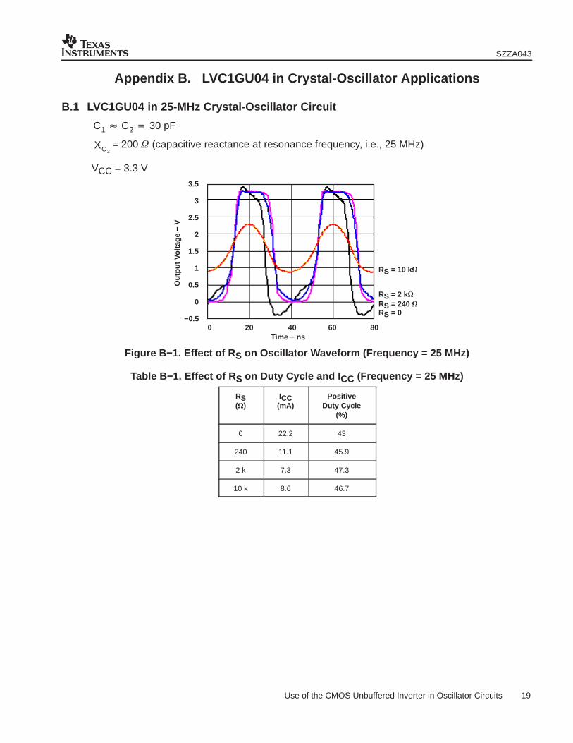
B.1 LVC1GU04 in 25-MHz Crystal-Oscillator Circuit
C1 C2 30 pF
2CX = 200 (capacitive reactance at resonance frequency, i.e., 25 MHz)
VCC = 3.3 V
Time − ns
RS = 240
3.5O
utpu
t Vol
tage
− V
0
3
2.5
2
1.5
1
0.5
0
−0.520 40 60 80
RS = 10 k
RS = 2 k
RS = 0
Figure B−1. Effect of R S on Oscillator Waveform (Frequency = 25 MHz)
Table B−1. Effect of R S on Duty Cycle and I CC (Frequency = 25 MHz)
RS()
ICC(mA)
PositiveDuty Cycle
(%)
0 22.2 43
240 11.1 45.9
2 k 7.3 47.3
10 k 8.6 46.7
SZZA043
20 Use of the CMOS Unbuffered Inverter in Oscillator Circuits
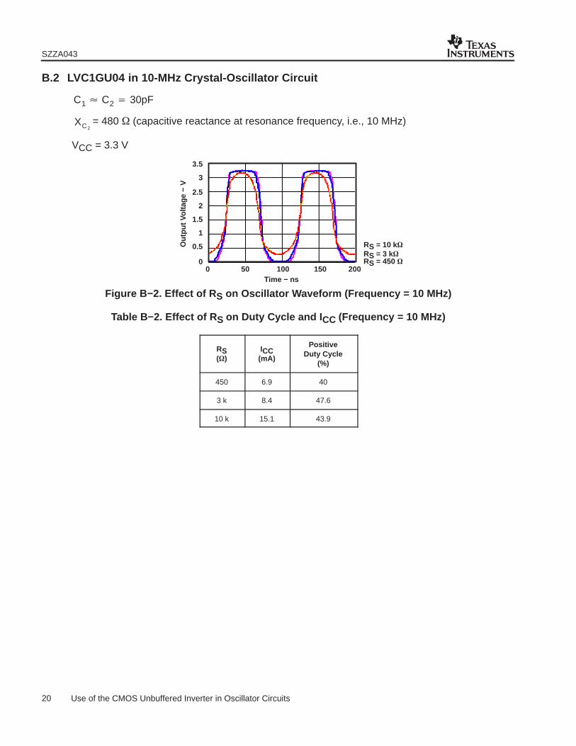
B.2 LVC1GU04 in 10-MHz Crystal-Oscillator Circuit
C1 C2 30pF
2CX = 480 (capacitive reactance at resonance frequency, i.e., 10 MHz)
VCC = 3.3 V
Time − ns
RS = 10 k
3.5
Out
put V
olta
ge −
V
0
3
2.5
2
1.5
1
0.5
050 100 150 200
RS = 3 kRS = 450
Figure B−2. Effect of R S on Oscillator Waveform (Frequency = 10 MHz)
Table B−2. Effect of R S on Duty Cycle and I CC (Frequency = 10 MHz)
RS()
ICC(mA)
PositiveDuty Cycle
(%)
450 6.9 40
3 k 8.4 47.6
10 k 15.1 43.9
SZZA043
21 Use of the CMOS Unbuffered Inverter in Oscillator Circuits
B.3 LVC1GU04 in 2-MHz Crystal-Oscillator Circuit
C1 C2 30pF
2CX = 2.4 k (capacitive reactance at resonance frequency, i.e., 2 MHz)
VCC = 3.3 V
RS = 10 k
3.5
Out
put V
olta
ge −
V
0
3
2.5
2
1.5
1
0.5
0200 400 600 800
RS = 2 kRS = 240
Time − ns
Figure B−3. Effect of R S on Oscillator Waveform (Frequency = 2 MHz)
Table B−3. Effect of R S on Duty Cycle and I CC (Frequency = 2 MHz)
RS()
ICC(mA)
PositiveDuty Cycle
(%)
240 11.1 45.9
2 k 7.3 47.3
10 k 8.6 46.7

SZZA043
22 Use of the CMOS Unbuffered Inverter in Oscillator Circuits
B.4 LVC1GU04 in 100-kHz Crystal-Oscillator Circuit
C1 C2 30pF
2CX = 48 k (capacitive reactance at resonance frequency, i.e., 100 kHz)
VCC = 3.3 V
RS = 220 k
0
3
2.5
2
1.5
1
0.5
05 10 15 20
RS = 100 kRS = 50 k
Out
put V
olta
ge −
V
Time − s
3.5
Figure B−4. Effect of R S on Oscillator Waveform (Frequency = 100 kHz)
Table B−4. Effect of R S on Duty Cycle and I CC (Frequency = 100 kHz)
RS()
ICC(mA)
PositiveDuty Cycle
(%)
50 k 9 46.4
100 k 9.5 46.1
220 k 13.7 44.3

SZZA043
23 Use of the CMOS Unbuffered Inverter in Oscillator Circuits
Appendix C. LVC1404 in Crystal-Oscillator Applications
C.1 LVC1404 in 25-MHz Crystal-Oscillator Circuit
C1 C2 30pF
RS =2CX = 200 (capacitive reactance at resonance frequency, i.e., 25 MHz)
VCC = 3.3 V
ICC = 8.6 mA
Duty cycle = 48.1%
0
2.52
1.51
0.50
4010 3020
Out
put V
olta
ge −
V
Time − ns
33.5
4
−0.5706050
Figure C−1. Output Waveform of Oscillator Circuit Using LVC1404 (Frequency = 25 MHz)

SZZA043
24 Use of the CMOS Unbuffered Inverter in Oscillator Circuits
C.2 LVC1404 in 100-kHz Crystal-Oscillator Circuit
C1 C2 30pF
RS =2CX = 48 k (capacitive reactance at resonance frequency, i.e., 100 kHz)
VCC = 3.3 V
ICC = 5.7 mA
Duty cycle = 47.4%
0
2.5
2
1.5
1
0.5
082 64
Out
put V
olta
ge −
V
Time − s
3
3.5
1210 14
Figure C−2. Output Waveform of Oscillator Circuit Using LVC1404 (Frequency = 100 kHz)

IMPORTANT NOTICE
Texas Instruments Incorporated and its subsidiaries (TI) reserve the right to make corrections, modifications,enhancements, improvements, and other changes to its products and services at any time and to discontinueany product or service without notice. Customers should obtain the latest relevant information before placingorders and should verify that such information is current and complete. All products are sold subject to TI’s termsand conditions of sale supplied at the time of order acknowledgment.
TI warrants performance of its hardware products to the specifications applicable at the time of sale inaccordance with TI’s standard warranty. Testing and other quality control techniques are used to the extent TIdeems necessary to support this warranty. Except where mandated by government requirements, testing of allparameters of each product is not necessarily performed.
TI assumes no liability for applications assistance or customer product design. Customers are responsible fortheir products and applications using TI components. To minimize the risks associated with customer productsand applications, customers should provide adequate design and operating safeguards.
TI does not warrant or represent that any license, either express or implied, is granted under any TI patent right,copyright, mask work right, or other TI intellectual property right relating to any combination, machine, or processin which TI products or services are used. Information published by TI regarding third-party products or servicesdoes not constitute a license from TI to use such products or services or a warranty or endorsement thereof.Use of such information may require a license from a third party under the patents or other intellectual propertyof the third party, or a license from TI under the patents or other intellectual property of TI.
Reproduction of information in TI data books or data sheets is permissible only if reproduction is withoutalteration and is accompanied by all associated warranties, conditions, limitations, and notices. Reproductionof this information with alteration is an unfair and deceptive business practice. TI is not responsible or liable forsuch altered documentation.
Resale of TI products or services with statements different from or beyond the parameters stated by TI for thatproduct or service voids all express and any implied warranties for the associated TI product or service andis an unfair and deceptive business practice. TI is not responsible or liable for any such statements.
Following are URLs where you can obtain information on other Texas Instruments products and applicationsolutions:
Products Applications
Amplifiers amplifier.ti.com Audio www.ti.com/audio
Data Converters dataconverter.ti.com Automotive www.ti.com/automotive
DSP dsp.ti.com Broadband www.ti.com/broadband
Interface interface.ti.com Digital Control www.ti.com/digitalcontrol
Logic logic.ti.com Military www.ti.com/military
Power Mgmt power.ti.com Optical Networking www.ti.com/opticalnetwork
Microcontrollers microcontroller.ti.com Security www.ti.com/security
Telephony www.ti.com/telephony
Video & Imaging www.ti.com/video
Wireless www.ti.com/wireless
Mailing Address: Texas Instruments
Post Office Box 655303 Dallas, Texas 75265
Copyright 2004, Texas Instruments Incorporated
Top Related