


Languages
Pages
Legal

UNIT- II VLSI DESIGN
Page 1
MOS and CMOS Circuit Design Process:
MOS and CMOS circuit design process involves the concepts such as:
MOS Layers
Stick Diagrams
Lambda based design rules and layout diagrams
Basic circuit concepts such as: sheet resistance, area capacitance and delay calculation
MOS Layers:
MOS circuits are formed by three layers i.e. diffusion ( n or p diffusion layer), polysilicon and metal, which
are isolated from one another by thick or thin (thinox) silicon dioxide insulating layers.
The thin oxide region includes n- diffusion, p- diffusion and transistor channels. Polysilicon and
thinox regions interact so that a transistor is formed where they cross one another.
Layers may be deliberately joined together where contacts are formed.
The basic MOS transistor properties can be modified by the use of an implant within the thinox
region.
The MOS design is aimed at turning a specification into masks for processing silicon to meet the
specification.
Stick Diagrams and Layout Diagrams:
Stick diagrams are used to convey layer information and topology through the use of color code and using
these stick diagrams mask layouts can be easily designed. The color code for various layers are:
1. Green for n- diffusion
2. Red for polysilicon
3. Blue for metal
4. Yellow for implant or for p- diffusion
5. Black for contact areas
The layout of stick diagrams faithfully reflects the topology of the actual layout in silicon and the
stick diagrams are relatively easily turned into mask layouts.
As known that the mask layout produced during design will be compatible with the fabrication
processes, a set of design rules are set out for layouts so that, if obeyed, the rules will produce layouts
which will work in practice.
Mask Layout/ Layout/ Layout Diagram represent an integrated circuit in terms of planar geometric shapes
which corresponds to the pattern of the metal, oxide or semiconductor layers that make up the components
of the integrated circuit. The dimensions of each layer and the separation between the layers in a layout are
parameterized by λ.

UNIT- II VLSI DESIGN
Page 2
Basic Encoding Concepts for Drawing stick diagrams and mask layout/ Layout Diagram:
Layers and their
color
Stick diagram encoding Mask layout encoding Monochrome
stick encoding
Monochro
me mask
encoding
n diffusion
color- green
p diffusion
color- yellow
Polysilicon
color- red
Implant
color- yellow
Metal 1
color- blue
Metal 2
color- dark blue
contact cut
(including
buried)
color- black
VDD or VSS
contact cut
color- black
via cut
color- black
Demarcation line/
pwell
color- brown
nMOS-
enhancement
mode
G
D S
pMOS-
enhancement
mode
G
S D
nMOS-
depletion mode
G
D S
pMOS-
depletion mode
G
S D
Green
Yellow
Yellow
Red
Blue
Dark Blue
Unburied contact cut
Buried contact cut
(brown color)
---------------------
---------------------------------
---------------------------------

UNIT- II VLSI DESIGN
Page 3
1. nMOS inverter:
CMOS Diagram Stick Diagram
Mask Layout/ Layout Diagram
VDD
Vout
Vin
VDD
Vout
Vin
GND
GND GND
Vin
VDD
Vout

UNIT- II VLSI DESIGN
Page 4
1. CMOS Inverter:
CMOS Diagram Stick Diagram
Mask Layout
Encodings Layers Colour Stick diagram Layout diagram Metal 1 Blue
n diffusion Green
p diffusion Yellow
Polysilicon Red
Implant Yellow
Contact Black
VDD
Vin Vout
Vss
Vin
VDD
Vout
Vss
VDD
Vss
Vout Vin
----------------------------------------------
-----------------------------------------------------------------------
-----------------------------------------------------------------------

UNIT- II VLSI DESIGN
Page 5
Design Rules:
Design rules provide an effective interface between the circuit/ system designer and the fabrication engineer.
Lambda Based Design rules and layout diagrams:
Lambda based design rules are based on a single parameter lambda λ which leads to a simple set of rules for
the designer, providing a process and feature size independent way of setting out mask dimensions to scale.
These rules specify line widths, separations, and extensions in terms of λ, and are readily committed to
memory.
All paths in all the layers will be dimensioned in λ units and subsequently λ can be allocated to an
appropriate value compatible with the feature size of the fabrication process i.e. if mask layout obey these
rules correctly in the layout, then the mask layout will produce working circuits for a range of values
allocated to λ.
Contacts between polysilicon and diffusion in nMOS/ MOS circuits are possible by two approaches:
1. Butting Contact
2. Buried Contact
The latter is generally less space- consuming and is held by many to be the more reliable contact. Therefore
consultation to the fabrication work where the designs are to be turned into silicon should be prior.
The layout diagrams are drawn on squared paper (say 5mm) where the side of each square is taken to
represent λ. The layout diagrams use the design rules using contacts such as butting contact where
departures from strict adherence to the rules can take place.
nMOS-
enhancement
mode
G
D S
pMOS-
enhancement
mode
G
S D
nMOS-
depletion mode
G
D S
pMOS-
depletion mode
G
S D
Illustrating λ based rule, using 2λ specification as width for the polysilicon and thinox layers
2λ
2λ
2λ
2λ
2λ
2λ
2λ
2λ

UNIT- II VLSI DESIGN
Page 6
Lambda based design rules for wires (nMOS and CMOS):
Layer width:
Layer Minimum Width
n- diffusion 2λ
p- diffusion 2λ
Polysilicon 2λ
Metal 1 3λ
Metal 2 4λ
Separation between the layers:
Layers Minimum Separation
n- diffusion and n- diffusion 3λ
p- diffusion and p- diffusion 3λ
Polysilicon and polysilicon 2λ
n-diffusion and polysilicon 1λ
p-diffusion and polysilicon 1λ
Metal 1 and metal 1 3λ
Metal 2 and metal 2 4λ
Basic circuit concepts:
Basic circuit concepts help us to calculate the actual resistance, capacitance, delay values associated with the
transistors and their circuit wiring and parasitic.
Sheet Resistance Rs:
Sheet resistance is defined as the ratio of resistivity ρ and thickness t for a sheet/ slab.
Consider a uniform slab of conducting material ρ of width W, thickness t, and length L between the faces A
and B, then the value of resistance of the slab (sheet) is given as,
𝑹𝑨𝑩 =𝝆𝑳
𝑨 𝒐𝒉𝒎
𝑹𝑨𝑩 =𝝆𝑳
𝒕 𝑾 𝒐𝒉𝒎
Where:
A = t W = area of cross section of the slab
If L = W, i.e. square of resistive material, then
𝑹𝑨𝑩 =𝝆
𝒕 = 𝑹𝒔 𝒊𝒏 𝒐𝒉𝒎 𝒔𝒒𝒖𝒂𝒓𝒆
B
A
L
thickness t
W
𝝆

UNIT- II VLSI DESIGN
Page 7
Where:
Rs = sheet resistance or ohm per square
For a MOSFET transistor
𝑹 = 𝒁𝑹𝒔 =𝑳
𝑾 𝑹𝒔 = 𝟒 × 𝟏𝟎𝟒𝒐𝒉𝒎
Where:
Z = L/ W
It is to be noted that Rs is completely independent of the area of the square.
The typical sheet resistances Rs for various MOS layers are (considering different technologies)
Layer Sheet Resistance Rs
5 μm Technology 2 μm Technology 1.2 μm Technology
Metal 0.03 0.04 0.04
n- channel transistor/
pMOS transistor
1×10⁴
2×10⁴ 2×10
4
p- channel transistor/
pMOS transistor
2.5×10⁴ 4.5×10
4 4.5×10
4
Diffusion 10- 50 10- 50 10- 50
Silicide 2- 4 2- 4 2- 4
Polysilicon 15- 100 15- 100 15- 100
Area Capacitance:
In MOS transistor conducting layers are separated from the substrate and each other by insulating
(dielectric) layers, and thus parallel plate capacitive effects are present and are allowed.
For any layer, knowing the dielectric (silicon dioxide) thickness, we can calculate area capacitance as,
𝑪 = 𝜺𝟎 𝜺𝒊𝒏𝒔 𝑨
𝑫=𝒌 𝑨
𝑫 𝒇𝒂𝒓𝒂𝒅𝒔
Where:
D = thickness of silicon dioxide
k = dielectric constant
A = Area of plates
𝜀𝑖𝑛𝑠 = 𝑟𝑒𝑙𝑎𝑡𝑖𝑣𝑒 𝑝𝑒𝑟𝑚𝑖𝑡𝑡𝑖𝑣𝑖𝑡𝑦 𝑜𝑓 𝑠𝑖𝑙𝑖𝑐𝑜𝑛 𝑑𝑖𝑜𝑥𝑖𝑑𝑒
𝜀0 = 𝑟𝑒𝑙𝑎𝑡𝑖𝑣𝑒 𝑝𝑒𝑟𝑚𝑖𝑡𝑡𝑖𝑣𝑖𝑡𝑦 𝑜𝑓 𝑓𝑟𝑒𝑒 𝑠𝑝𝑎𝑐𝑒 = 8.85 × 10⁻¹⁴𝐹/ 𝑐𝑚

UNIT- II VLSI DESIGN
Page 8
Normally area capacitances are given in pF/ μm2 (where μm = micron = 10
-6 meter = 10
-4 cm). The
appropriate figure may be calculated as:
𝐶 𝑝𝐹
𝜇𝑚2 =
𝜀0 𝜀𝑖𝑛𝑠
𝐷
𝐹
𝑐𝑚2×
1012𝑝𝐹
𝐹×
𝑐𝑚2
108𝜇𝑚2
The typical area capacitance values for 5μm MOS circuits are:
Capacitance Value in pF/ μm2
Relative value
Gate to Channel 4×10⁻⁴
1
Diffusion to substrate 1×10⁻⁴
0.25
Polysilicon to substrate 0.4×10⁻⁴
0.1
Metal 1 to substrate 0.3×10⁻⁴
0.075
Metal 2 to substrate 0.2×10⁻⁴
0.05
Metal 2 to metal 1 0.4×10⁻⁴
0.1
Metal 2 to polysilicon 0.3×10⁻⁴
0.075
Note: Relative value = Specified value / gate to channel value
o Standard unit of capacitance " 𝑪𝒈":
The standard unit of capacitance is denoted by 𝑪𝒈 and is defined as the gate- to- channel capacitance of
the minimum size (2λ × 2λ) MOS transistor.
The standard unit of capacitance has provided a convenience to various MOS technologies but which
can be used in calculations without associating it with an absolute value.
𝑪𝒈 can be evaluated for any MOS technology.
For example for a 5 µm MOS circuit with λ = 2.5 µm:
Gate area = 5 µm × 5 µm = 25 µm2
Capacitance value = 4 × 10
-4 pF/ µm
2 (using table)
Standard Capacitance 𝑪𝒈= 25 µm
2 × 4 × 10
-4 pF/ µm
2 = .01 pF
o Some Area Capacitance calculations:
Here the calculation of capacitance values may now be done by the ratio between the area of interest
and the area of the standard gate (2λ × 2λ) and multiplying this ratio by the appropriate relative C
value (using the table). The product will give the required capacitance in 𝐶𝑔 units.
Let’s calculate the capacitance of a simple area of length 20λ and width 3λ respectively.
Now we will calculate: L = 20λ
W= 3λ
UNIT- II VLSI DESIGN
Page 9
1. Relative Area
𝑅𝑒𝑙𝑎𝑡𝑖𝑣𝑒 𝐴𝑟𝑒𝑎 =𝐿 × 𝑊
2λ × 2λ=
20𝜆 × 3𝜆
2λ × 2λ= 15
2. Capacitance to substrate considering the area in metal.
𝐶𝑎𝑝𝑎𝑐𝑖𝑡𝑎𝑛𝑐𝑒 𝑡𝑜 𝑠𝑢𝑏𝑠𝑡𝑟𝑎𝑡𝑒 = 𝑟𝑒𝑙𝑎𝑡𝑖𝑣𝑒 𝑎𝑟𝑒𝑎 × 𝑟𝑒𝑙𝑎𝑡𝑖𝑣𝑒 𝐶 𝑣𝑎𝑙𝑢𝑒 𝑓𝑟𝑜𝑚 𝑡𝑎𝑏𝑙𝑒
𝐶𝑎𝑝𝑎𝑐𝑖𝑡𝑎𝑛𝑐𝑒 𝑡𝑜 𝑠𝑢𝑏𝑠𝑡𝑟𝑎𝑡𝑒 = 15 × 0.075 𝐶𝑔
3. Capacitance to substrate considering the area in polysilicon.
𝐶𝑎𝑝𝑎𝑐𝑖𝑡𝑎𝑛𝑐𝑒 𝑡𝑜 𝑠𝑢𝑏𝑠𝑡𝑟𝑎𝑡𝑒 = 𝑟𝑒𝑙𝑎𝑡𝑖𝑣𝑒 𝑎𝑟𝑒𝑎 × 𝑟𝑒𝑙𝑎𝑡𝑖𝑣𝑒 𝐶 𝑣𝑎𝑙𝑢𝑒 𝑓𝑟𝑜𝑚 𝑡𝑎𝑏𝑙𝑒
𝐶𝑎𝑝𝑎𝑐𝑖𝑡𝑎𝑛𝑐𝑒 𝑡𝑜 𝑠𝑢𝑏𝑠𝑡𝑟𝑎𝑡𝑒 = 15 × 0.1 𝐶𝑔 = 1.5 𝐶𝑔
4. Capacitance to substrate considering the area in diffusion.
𝐶𝑎𝑝𝑎𝑐𝑖𝑡𝑎𝑛𝑐𝑒 𝑡𝑜 𝑠𝑢𝑏𝑠𝑡𝑟𝑎𝑡𝑒 = 𝑟𝑒𝑙𝑎𝑡𝑖𝑣𝑒 𝑎𝑟𝑒𝑎 × 𝑟𝑒𝑙𝑎𝑡𝑖𝑣𝑒 𝐶 𝑣𝑎𝑙𝑢𝑒 𝑓𝑟𝑜𝑚 𝑡𝑎𝑏𝑙𝑒
𝐶𝑎𝑝𝑎𝑐𝑖𝑡𝑎𝑛𝑐𝑒 𝑡𝑜 𝑠𝑢𝑏𝑠𝑡𝑟𝑎𝑡𝑒 = 15 × 0.25 𝐶𝑔 = 3.75 𝐶𝑔
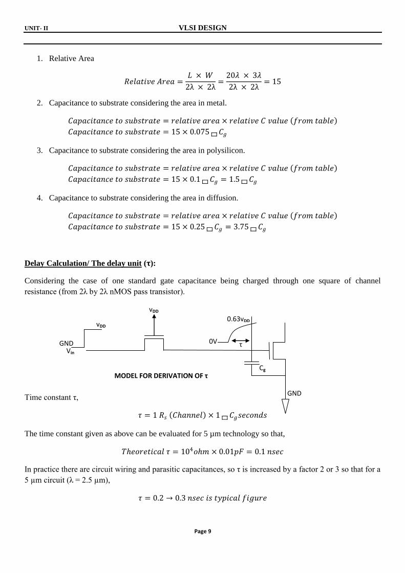
Delay Calculation/ The delay unit (𝛕):
Considering the case of one standard gate capacitance being charged through one square of channel
resistance (from 2λ by 2λ nMOS pass transistor).
Time constant τ,
𝜏 = 1 𝑅𝑠 𝐶𝑎𝑛𝑛𝑒𝑙 × 1 𝐶𝑔𝑠𝑒𝑐𝑜𝑛𝑑𝑠
The time constant given as above can be evaluated for 5 µm technology so that,
𝑇𝑒𝑜𝑟𝑒𝑡𝑖𝑐𝑎𝑙 𝜏 = 104𝑜𝑚 × 0.01𝑝𝐹 = 0.1 𝑛𝑠𝑒𝑐
In practice there are circuit wiring and parasitic capacitances, so τ is increased by a factor 2 or 3 so that for a
5 µm circuit (λ = 2.5 µm),
𝜏 = 0.2 → 0.3 𝑛𝑠𝑒𝑐 𝑖𝑠 𝑡𝑦𝑝𝑖𝑐𝑎𝑙 𝑓𝑖𝑔𝑢𝑟𝑒
GND 0V
GND
vDD
0.63vDD
Vin
Cg
τ
vDD
MODEL FOR DERIVATION OF τ

UNIT- II VLSI DESIGN
Page 10
It is to be noted that τ thus obtained is not much different from transit time τsd, which is given as,
τsd =L2
μnVds
Inverter Delays:
Considering a basic 4:1 ratio nMOS inverter in order to achieve the 4:1 Zpu to Zpd ratio, Rpu will be 4 Rpd,
and if Rpd is contributed by the minimum size transistor then, clearly, the resistance value associated with
Rpu is such,
𝑅𝑝𝑢 = 4𝑅𝑠 = 40 𝑘Ω
The Rpd value is 1 Rs = 10 kΩ so that the delay associated with the inverter will depend on whether it
is being turned on or off and if considering the pair of cascaded inverters, then delay over the pair will
be constant irrespective of the sense of the logic level transition of the input to the first. (Assuming
τ = 0.3 nsec and making no extra allowances fro wiring capacitance). We have an overall delay
of τ + 4τ = 5τ.
In general terms the delay through a pair of similar nMOS inverters is
Td = 1 +Zpu
Zpd τ
Thus, the inverter pair delay for inverters having 4:1 ratio is 5τ (which should be multiplied by a suitable
factor to allow for wiring).
1τ 4τ
5τ
Vin
4:1 4:1
Cg Cg

UNIT- II VLSI DESIGN
Page 11
Formal Estimation of CMOS inverter delay:
A CMOS inverter in general either charges or discharges a capacitive load CL and rise time τr , or fall time τf
can be estimated from the following analaysis:
1. Rise time estimation:
Here, we assume that the p- device stays in saturation for the entire charging period of the load
capacitor CL. The circuit may then be modelled as shown.
The saturation current for the p- transistor is given as,
𝐼𝑑𝑠𝑝 =𝛽𝑝 𝑉𝑔𝑠 − 𝑉𝑡𝑝
2
2
This current charges CL and, since its magnitude is approximately constant, we have
𝑉𝑜𝑢𝑡 =𝐼𝑑𝑠𝑝 𝑡
𝐶𝐿
Substituting 𝐼𝑑𝑠𝑝 =𝛽𝑝 𝑉𝑔𝑠− 𝑉𝑡𝑝
2
2 in 𝑉𝑜𝑢𝑡 =
𝐼𝑑𝑠𝑝 𝑡
𝐶𝐿, we get
𝑉𝑜𝑢𝑡 =
𝛽𝑝 𝑉𝑔𝑠 − 𝑉𝑡𝑝 2
2 𝑡
𝐶𝐿
𝑡 =2 𝐶𝐿𝑉𝑜𝑢𝑡
𝛽𝑝 𝑉𝑔𝑠 − 𝑉𝑡𝑝 2
Assuming that t = τrwhen 𝑉𝑜𝑢𝑡 = +𝑉𝐷𝐷 , so that
τr =2 𝐶𝐿𝑉𝐷𝐷
𝛽𝑝 𝑉𝐷𝐷 − 𝑉𝑡𝑝 2
With 𝑉𝑡𝑝 = 0.2 𝑉𝐷𝐷 , 𝑡𝑒𝑛
𝛕𝐫 =𝟑 𝑪𝑳
𝜷𝒑 𝑽𝑫𝑫
Algebraically,
𝛕𝐫 = 𝟐.𝟐𝛕𝐩
Therefore, the charging of CL is divided more correctly into two parts i.e. saturation and the resistive region
of the transistor.
VDD
VSS
CL Vout
Idsp
Vin = Vgs
1
0
1
0
UNIT- II VLSI DESIGN
Page 12
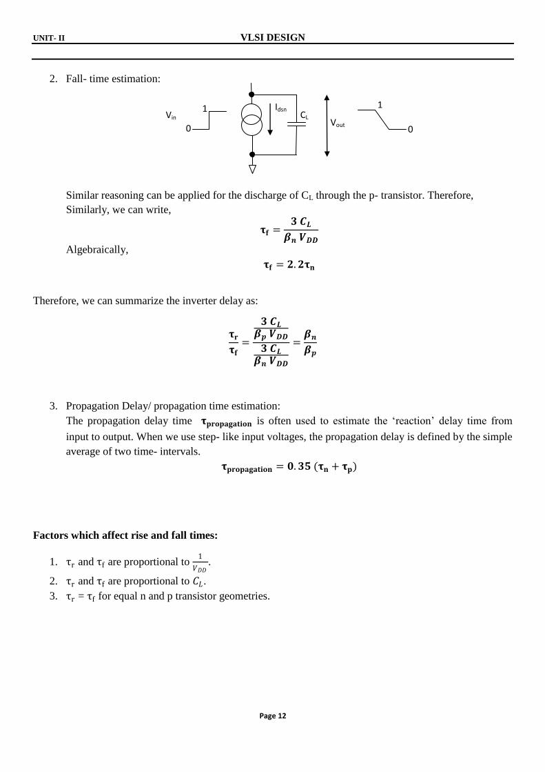
2. Fall- time estimation:
Similar reasoning can be applied for the discharge of CL through the p- transistor. Therefore,
Similarly, we can write,
𝛕𝐟 =𝟑 𝑪𝑳
𝜷𝒏 𝑽𝑫𝑫
Algebraically,
𝛕𝐟 = 𝟐.𝟐𝛕𝐧
Therefore, we can summarize the inverter delay as:
𝛕𝐫𝛕𝐟
=
𝟑 𝑪𝑳𝜷𝒑 𝑽𝑫𝑫𝟑 𝑪𝑳
𝜷𝒏 𝑽𝑫𝑫
=𝜷𝒏
𝜷𝒑
3. Propagation Delay/ propagation time estimation:
The propagation delay time 𝛕𝐩𝐫𝐨𝐩𝐚𝐠𝐚𝐭𝐢𝐨𝐧 is often used to estimate the ‘reaction’ delay time from
input to output. When we use step- like input voltages, the propagation delay is defined by the simple
average of two time- intervals.
𝛕𝐩𝐫𝐨𝐩𝐚𝐠𝐚𝐭𝐢𝐨𝐧 = 𝟎.𝟑𝟓 (𝛕𝐧 + 𝛕𝐩)
Factors which affect rise and fall times:
1. τr and τf are proportional to 1
𝑉𝐷𝐷.
2. τr and τf are proportional to 𝐶𝐿.
3. τr = τf for equal n and p transistor geometries.
CL Idsn
Vout Vin
1
0
1
0

UNIT- II VLSI DESIGN
Page 13
Super buffer:
A super buffer is a common alleviative approach for undesirable rise of delay problems of an conventional
inverter/ inverter when it is used to drive more significant capacitive loads.
There are two types of super buffers:
1. Inverting type of super buffer
2. Non inverting type of super buffer
Inverting type super buffer (nMOS):
The inverting type as shown above is considered with a positive going logic transition Vin at the input, it is
seen that the inverter formed by T1 and T2 is turned ON and thus the gate T3 is pulled down toward 0V with
a small delay. Thus T3 is cut off while T4 (the gate of which is also connected to Vin) is turned ON and the
output is pulled down quickly.
Now considering the opposite transition, when Vin drops to 0V then the gate of T3 is allowed to rise quickly
to VDD. Thus as T4 is also turned OFF by Vin, T3 is caused to conduct with VDD on its gate, that is, with twice
the average voltage which would apply if the gate was tied to the source as in the conventional inverter.
Since Ids is directly proportional to Vgs, then it doubles the effective Vgs will increase the current and thus
reduce the delay in charging any capacitance on the output. Thus more symmetrical transitions are achieved.
Non inverting type buffer (nMOS):
VDD
T1
T2
T3
T4 Vin
Vout
VDD
T1
T2
T3
T4 Vin
Vout

UNIT- II VLSI DESIGN
Page 14
The corresponding non inverting buffer as shown which has perspective structure of driving loads of 2 pF
and with 5 nsec risetime.
If the inverting or non inverting buffer is arranged based on the native transistor, then it is known as native
super buffer.
Channel Length Modulation and Velocity Saturation:
The voltages exceeding the onset of saturation there is an effective decrease in the channel length of short
channel transistor, this is referred as channel length modulation.
For example, the change in channel length ΔL for a n- transistor is approximated by,
∆𝐿 = 2 𝜀0 𝜀𝑆𝑖𝑞 𝑁𝐴
𝑉𝑑𝑠 − 𝑉𝑡
And the resultant drain to source current 𝐼1𝑑𝑠 is approximated by,
𝐼1𝑑𝑠 = 𝐼𝑑𝑠
𝐿
𝐿 − ∆𝐿
Velocity Saturation:
When the drain to source voltage of a short channel transistor exceeds a critical value, the charge carriers
reach their maximum scattering limited velocity before pinch off. Thus less current is available from a short
channel transistor than from a long channel transistor with similar width to length ratio and processing.
Therefore, channel length modulation and velocity saturation are the two effects important for short channel
transistors, i.e. channel lengths ≤ 3 µm, and these effects should be taken into account.
Fan-in and Fan- out:
The number of inputs to a logic gate in an inverter while adding complementary transistor pairs which
increases the delay times as the capacitance of the transistor is increased is called fan- in (FI) and the
number of gates is specified by the fan- out (FO) of the circuit. The fan- out gates acts as a load to the
driving circuit because of their input capacitance.

UNIT- II VLSI DESIGN
Page 15
Problems:
1. A resistor of value 100 kΩ needs to be made from a resistive layer of thickness 1µm. If the resistivity
of the material is 1 Ωcm and the strip of width 5 µm is used, then what should be the length of the
strip?
Sol.
Given:
R = 100 kΩ = 1000×103 Ω
ρ = 1 Ωcm = 1×10⁻²
t = 1 µm = 1×10⁻⁶
m
W = 5 µm = 5×10⁻⁶
m
To find:
L = ?
WKT,
𝑅 =𝜌 𝐿
𝑡 𝑊
𝐿 =𝑅 𝑡 𝑊
𝜌=
1000 × 103 × 1 × 10−6 × 5 × 10−6
1 × 10−2= 5 × 10⁻⁵𝑚
Therefore, the length of the strip is 5 × 10⁻⁵𝑚 respectively.
2. A layer of MOS circuit has a resistivity of 1 Ωcm, a section of this material is 5 µm thick, 5 µm wide
and has a length of 50 µm, calculate the resistance from one of the section to the other using the
concept of sheet resistance.
Sol.
Given:
ρ = 1 Ωcm = 1×10⁻²
t = 5 µm = 5×10⁻⁶
m
W = 5 µm = 5×10⁻⁶
m
L = 50 µm = 50×10-6
m

UNIT- II VLSI DESIGN
Page 16
To find:
R = ? using Rs, so first finding Rs also
WKT,
𝑅𝑠 =𝜌
𝑡=
1 × 10⁻²
5 × 10−6= 0.2 × 10⁴ 𝑜𝑚
𝑠𝑞𝑢𝑎𝑟𝑒
And
𝑅 = 𝑅𝑠𝐿
𝑊= 0.2 × 104 ×
50 × 10−6
5 × 10−6= 2 × 10⁴𝛺
Therefore, the value of resistance is 2×10⁴ Ω respectively.
3. For the given transistor structure, calculate the channel resistance in 5 µm, 2 µm and 1.2 µm
technologies?
Sol.
Given:
L = 4λ
W = 2λ
For nMOS:
o In 5 µm technology
WKT,
4λ
2λ
S D

UNIT- II VLSI DESIGN
Page 17
𝑅 = 𝑅𝑠 ×𝐿
𝑊= 1 × 104 ×
4λ
2λ= 2 × 10⁴𝛺
o In 2 µm technology
WKT,
𝑅 = 𝑅𝑠 ×𝐿
𝑊= 2 × 104 ×
4λ
2λ= 40 𝑘𝛺
o In 1.2 µm technology
WKT,
𝑅 = 𝑅𝑠 ×𝐿
𝑊= 2 × 104 ×
4λ
2λ= 40 𝑘𝛺
For pMOS:
o In 5 µm technology
WKT,
𝑅 = 𝑅𝑠 ×𝐿
𝑊= 2.5 × 104 ×
4λ
2λ= 50 𝑘𝛺
o In 2 µm technology
WKT,
𝑅 = 𝑅𝑠 ×𝐿
𝑊= 4.5 × 104 ×
4λ
2λ= 90 𝑘𝛺
o In 1.2 µm technology
WKT,
𝑅 = 𝑅𝑠 ×𝐿
𝑊= 4.5 × 104 ×
4λ
2λ= 90 𝑘𝛺
Therefore, the channel resistance of the given transistor are found.

UNIT- II VLSI DESIGN
Page 18
4. For the given nMOS inverter, calculate the total resistance in 5 µm and 2 µm techmologies.
Sol.
Given:
The inverter has two transistors T1 with L = 4 and W = 1 and transistor T2 with L = 1
and W = 1.
o In 5 µm technology
WKT,
𝑅 = 𝑅𝑠 ×𝐿
𝑊
𝑅𝑇𝑜𝑡𝑎𝑙 = 𝑅𝑇1+ 𝑅𝑇2
𝑅𝑇𝑜𝑡𝑎𝑙 = 1 × 104 ×4
1 + 1 × 104 ×
1
1 = 50 𝑘𝛺
o In 2 µm technology
WKT,
𝑅 = 𝑅𝑠 ×𝐿
𝑊
𝑅𝑇𝑜𝑡𝑎𝑙 = 𝑅𝑇1+ 𝑅𝑇2
𝑅𝑇𝑜𝑡𝑎𝑙 = 2 × 104 ×4
1 + 2 × 104 ×
1
1 = 100 𝑘𝛺
Therefore, the total resistance of the inverter in 5 µm technology is 50 kΩ and in 2µm technology is
100 kΩ respectively.
4:1
1:1
T1
T2

UNIT- II VLSI DESIGN
Page 19
Assignment: (a) Draw the stick diagrams and mask layouts/ layout diagrams of the following and also find
the total channel resistance of the nMOS NAND and NOR gates given:
1. nMOS and CMOS NAND Gate:
Circuit symbol of nMOS NAND Gate Circuit symbol of CMOS NAND Gate
2. nMOS and CMOS NOR Gate:
Circuit symbol of nMOS NOR Gate Circuit symbol of CMOS NOR Gate
A
B
C
GND
VDD
A
VDD
C
GND
B
VDD
C
GND
A
B
VDD
GND
C
A
B
4:1
1:1
1:1
4:1
1:2
1:2

UNIT- II VLSI DESIGN
Page 20
(b) For the given transistor structure, calculate the channel resistance in 5 µm, 2 µm and 1.2 µm
technologies?
(c) Calculate the total resistance in a CMOS inverter in 5 µm, 2 µm and 1.2 µm technologies?
(Note/ Hint : For CMOS inverter 𝐿:𝑊 = 1 ∶ 1 𝑖. 𝑒. 𝐿
𝑊=
1
1 )
2λ
8λ
Top Related