


Languages
Pages
Legal


1/74January 2002
HIGH PERFORMANCE CPU
– 16-BIT CPU WITH 4-STAGE PIPELINE– 80ns INSTRUCTION CYCLE TIME AT 25MHz
CPU CLOCK– 400ns 16 X 16-BIT MULTIPLICATION– 800ns 32 / 16-BIT DIVISION– ENHANCED BOOLEAN BIT MANIPULATION
FACILITIES– ADDITIONAL INSTRUCTIONS TO SUPPORT
HLL AND OPERATING SYSTEMS– SINGLE-CYCLE CONTEXT SWITCHING SUP-
PORT
MEMORY ORGANIZATION
– 256K BYTE ON-CHIP FLASH MEMORY– 10K ERASING / PROGRAMMING CYCLES– UP TO 16M BYTE LINEAR ADDRESS SPACE
FOR CODE AND DATA (5M BYTE WITH CAN)– 2K BYTE ON-CHIP INTERNAL RAM (IRAM)– 6K BYTE ON-CHIP EXTENSION RAM (XRAM)– 20 YEAR DATA RETENTION TIME
FAST AND FLEXIBLE BUS
– PROGRAMMABLE EXTERNAL BUS CHARAC-TE- RISTICS FOR DIFFERENT ADDRESSRANGES
– 8-BIT OR 16-BIT EXTERNAL DATA BUS– MULTIPLEXED OR DEMULTIPLEXED EXTER-
NAL ADDRESS / DATA BUSES– FIVE PROGRAMMABLE CHIP-SELECT SIGNALS– HOLD-ACKNOWLEDGE BUS ARBITRATION
SUPPORT
INTERRUPT
– 8-CHANNEL PERIPHERAL EVENT CONTROL-LER FOR SINGLE CYCLE, INTERRUPT DRIVENDATA TRANSFER
– 16-PRIORITY-LEVEL INTERRUPT SYSTEMWITH 56 SOURCES, SAMPLE-RATE DOWN TO40ns
TIMERS
– TWO MULTI-FUNCTIONAL GENERAL PUR-POSE TIMER UNITS WITH 5 TIMERS
– TWO 16-CHANNEL CAPTURE / COMPAREUNITS.
4-CHANNEL PWM UNIT
SERIAL CHANNELS
– SYNCHRONOUS / ASYNCHRONOUS SERIALCHANNEL
– HIGH-SPEED SYNCHRONOUS CHANNEL
A/D CONVERTER– 16-CHANNEL 10-BIT– 7.76µS CONVERSION TIME
FAIL-SAFE PROTECTION– PROGRAMMABLE WATCHDOG TIMER– OSCILLATOR WATCHDOG
ON-CHIP CAN 2.0B INTERFACE
ON-CHIP BOOTSTRAP LOADER
CLOCK GENERATION– ON-CHIP PLL– DIRECT OR PRESCALED CLOCK INPUT.
UP TO 111 GENERAL PURPOSE I/O LINES– INDIVIDUALLY PROGRAMMABLE AS INPUT,
OUTPUT OR SPECIAL FUNCTION.– PROGRAMMABLE THRESHOLD (HYSTERESIS)
IDLE AND POWER DOWN MODES
SINGLE VOLTAGE SUPPLY: 5V ±10%
144-PIN PQFP PACKAGE
PQFP144 (28 x 28 mm)(Plastic Quad Flat Pack)
P.6 P.5 P.3
P..2
GP
Ts
AS
C
BRG
FLASHCPU Core
Watchdog
Interrupt controller
PEC
P.7 P.8
EB
C
AD
C
BRG
SS
C
PW
M
CA
PC
OM
2
CA
PC
OM
1
RAM
XR
AM
CA
N
OSC
P.1
P.0
P.4
ST10F168
16-BIT MCU WITH 256K BYTE FLASH MEMORY AND 8K BYTE RAM
This is advance information on a new product now in development or undergoing evaluation. Details are subject to change without notice.

ST10F168
2/74
1 INTRODUCTION ......................................................................................................... 4
2 PIN DATA ................................................................................................................... 5
3 FUNCTIONAL DESCRIPTION.................................................................................... 10
4 MEMORY ORGANIZATION........................................................................................ 11
5 FLASH MEMORY ....................................................................................................... 135.1 PROGRAMMING / ERASING WITH ST EMBEDDED ALGORITHM KERNEL ......... . 145.2 PROGRAMMING EXAMPLES .................................................................................... 165.3 FLASH MEMORY CONFIGURATION........................................................................ . 185.4 FLASH PROTECTION ................................................................................................ 185.5 BOOTSTRAP LOADER MODE................................................................................... 18
6 CENTRAL PROCESSING UNIT (CPU) ...................................................................... 196.1 INSTRUCTION SET SUMMARY................................................................................. 20
7 EXTERNAL BUS CONTROLLER............................................................................... 22
8 INTERRUPT SYSTEM ................................................................................................ 23
9 CAPTURE / COMPARE (CAPCOM) UNIT ................................................................. 26
10 GENERAL PURPOSE TIMER UNIT............................. .............................................. 2810.1 GPT1 ................................ ........................................................................................... 2810.2 GPT2 ................................ ........................................................................................... 28
11 PWM MODULE ........................................................................................................... 31
12 PARALLEL PORTS.................................................................................................... 32
13 A/D CONVERTER....................................................................................................... 33
14 SERIAL CHANNELS .................................................................................................. 34
15 CAN MODULE ............................................................................................................ 36
16 WATCHDOG TIMER................................................................................................... 36
17 SYSTEM RESET......................................................................................................... 3717.1 ASYNCHRONOUS RESET (LONG HARDWARE RESET) ........................................ 3717.2 SYNCHRONOUS RESET (WARM RESET) ................. .............................................. 3817.3 SOFTWARE RESET ................................................................................................... 3917.4 WATCHDOG TIMER RESET...................................................................................... 3917.5 RESET CIRCUITRY........ ........................................................................................... 39
18 POWER REDUCTION MODES .............................................................. .................... 42
TABLE OF CONTENT PAGE

ST10F168
3/74
19 SPECIAL FUNCTION REGISTER OVERVIEW.......................................................... 4319.1 IDENTIFICATION REGISTERS .................................................................................. 49
20 ELECTRICAL CHARACTERISTICS .......................................................................... 5020.1 ABSOLUTE MAXIMUM RATINGS.............................................................................. 5020.2 PARAMETER INTERPRETATION.............................................................................. 5020.3 DC CHARACTERISTICS ............................................................................................ 5020.4 A/D CONVERTER CHARACTERISTICS.................................................................... 5220.5 AC CHARACTERISTICS............................................................................................. 5320.5.1 Test Waveforms ........................................................................................................ 5320.5.2 Definition of Internal Timing......................................................................................... 5420.5.3 Clock Generation Modes ............................................................................................. 5420.5.4 Prescaler Operation..................................................................................................... 5520.5.5 Direct Drive.................................................................................................................. 5520.5.6 Oscillator Watchdog (OWD) ........................................................................................ 5520.5.7 Phase Locked Loop.......... ........................................................................................... 5520.5.8 External Clock Drive XTAL1.................................................................... .................... 5620.5.9 Memory Cycle Variables.............................................................................................. 5720.5.10 Multiplexed Bus ........................................................................................................... 5720.5.11 Demultiplexed Bus....................................................................................................... 6320.5.12 CLKOUT and READY.................................................................................................. 6920.5.13 External Bus Arbitration............................................................................................... 71
21 PACKAGE MECHANICAL DATA .............................................................................. 73
22 ORDERING INFORMATION ....................................................................................... 73

ST10F168
4/74
1 - INTRODUCTION
The ST10F168 is a derivative of the STMicroelec-tronics 16-bit single-chip CMOS microcontrollers.It combines high CPU performance (up to12.5 million instructions per second) with high
peripheral functionality and enhanced I/O capabil-ities. It also provides on-chip high-speed Flashmemory, on-chip high-speed RAM, and clock gen-eration via PLL.
Figure 1 : Logic Symbol
XTAL1
RSTIN
XTAL2
RSTOUT
NMI
EA
READY
ALE
RD
WR/WRL
Port 516-bit
Port 68-bit
Port 48-bit
Port 315-bit
Port 216-bit
Port 116-bit
Port 016-bit
VDD VSS
Port 78-bit
Port 88-bit
VAREF
VAGND ST10F168
VPP

ST10F168
5/74
2 - PIN DATA
Figure 2 : Pin Configuration (top view)
EAALE
RDVSSVDD
P6.0/CS0P6.1/CS1P6.2/CS2P6.3/CS3P6.4/CS4
P6.5/HOLDP6.6/HLDAP6.7/BREQ
P8.0/CC16IOP8.1/CC17IOP8.2/CC18IOP8.3/CC19IOP8.4/CC20IO
P8.6/CC22IOP8.7/CC23IO
VDDVSS
P7.0/POUT0P7.1/POUT1P7.2/POUT2P7.3/POUT3
P8.5/CC21IO
VPP/RPD
P7.4/CC28I0P7.5/CC29I0P7.6/CC30I0P7.7/CC31I0
P5.0/AN0P5.1/AN1P5.2/AN2P5.3/AN3P5.4/AN4P5.5/AN5P5.6/AN6P5.7/AN7P5.8/AN8P5.9/AN9
P0H.0/AD8P0L.7/AD7P0L.6/AD6P0L.5/AD5P0L.4/AD4P0L.3/AD3P0L.2AD2P0L.1/AD1P0L.0/AD0
READYWR/WRL
P4.7/A23P4.6/A22/CAN_TxDP4.5/A21/CAN_RxDP4.4/A20P4.3/A19P4.2/A18P4.1/A17P4.0/A16
VSSVDDP3.15/CLKOUTP3.13/SCLKP3.12/BHE/WRHP3.11/RXD0P3.10/TXD0P3.9/MTSRP3.8/MRSTP3.7/T2INP3.6/T3IN
VA
RE
FV
AG
ND
P5.
10/A
N10
/T6E
UD
P5.
11/A
N11
/T5E
UD
P5.
12/A
N12
/T6I
NP
5.13
/AN
13/T
5IN
P5.
14/A
N14
/T4E
UD
P5.
15/A
N15
/T2E
UD
VS
SV
DD
P2.
0/C
C0I
OP
2.1/
CC
1IO
P2.
2/C
C2I
OP
2.3/
CC
3IO
P2.
4/C
C4I
OP
2.5/
CC
5IO
P2.
6/C
C6I
OP
2.7/
CC
7IO
VS
SV
DD
P2.
8/C
C8I
O/E
X0I
NP
2.9/
CC
9IO
/EX
1IN
P2.
10/C
C10
IOE
X2I
NP
2.11
/CC
11IO
EX
3IN
P2.
12/C
C12
IO/E
X4I
NP
2.13
/CC
13IO
/EX
5IN
P2.
14/C
C14
IO/E
X6I
NP
2.15
/CC
15IO
/EX
7IN
/T7I
NP
3.0/
T0I
NP
3.1/
T6O
UT
P3.
2/C
AP
INP
3.3/
T3O
UT
P3.
4/T
3EU
DP
3.5/
T4I
NV
SS
VD
D
VS
SN
MI
VD
D
RS
TO
UT
RS
TIN
VS
SX
TA
L1X
TA
L2V
DD
P1H
.7/A
15/C
C27
IOP
1H.6
/A14
/CC
26IO
P1H
.5/A
13/C
C25
IOP
1H.4
/A12
/CC
24IO
P1H
.3/A
11P
1H.2
/A10
P1H
.1/A
9P
1H.0
/A8
VS
SV
DD
P1L
.7/A
7P
1L.6
/A6
P1L
.5/A
5P
1L.4
/A4
P1L
.3/A
3P
1L.2
/A2
P1L
.1/A
1P
1L.0
/A0
P0H
.7/A
D15
P0H
.6/A
D14
P0H
.5/A
D13
P0H
.4/A
D12
P0H
.3/A
D11
P0H
.2/A
D10
P0H
.1/A
D9
VS
SV
DD
123456789101112131415161718192021222324252627282930313233343536
37 38 39 40 41 42 43 44 45 46 47 48 49 50 51 52 53 54 55 56 57 58 59 60 61 62 63 64 65 66 67 68 69 70 71 72
108107106105104103102101100999897969594939291908988878685848382818079787776757473
144
143
142
141
140
139
138
137
136
135
134
133
132
131
130
129
128
127
126
125
124
123
122
121
120
119
118
117
116
115
114
113
112
111
110
109
ST10F168

ST10F168
6/74
Table 1 : Pin Description
Symbol Pin Type Function
P6.0 - P6.7 1 - 8 I/O 8-bit bidirectional I/O port, bit-wise programmable for input or output via direction bit.Programming an I/O pin as input forces the corresponding output driver to highimpedance state. Port 6 outputs can be configured as push-pull or open draindrivers. The following Port 6 pins have alternate functions:
1 O P6.0 CS0 Chip Select 0 Output
... ... ... ... ...
5 O P6.4 CS4 Chip Select 4 Output
6 I P6.5 HOLD External Master Hold Request Input
7 O P6.6 HLDA Hold Acknowledge Output
8 O P6.7 BREQ Bus Request Output
P8.0 - P8.7 9-16 I/O 8-bit bidirectional I/O port, bit-wise programmable for input or output via direction bit.Programming an I/O pin as input forces the corresponding output driver to highimpedance state. Port 8 outputs can be configured as push-pull or open draindrivers. The input threshold of Port 8 is selectable (TTL or special).The following Port 8 pins have alternate functions:
9 I/O P8.0 CC16IO CAPCOM2: CC16 Capture Input / Compare Output
... ... ... ... ...
16 I/O P8.7 CC23IO CAPCOM2: CC23 Capture Input / Compare Output
P7.0 - P7.7 19-26 I/O 8-bit bidirectional I/O port, bit-wise programmable for input or output via direction bit.Programming an I/O pin as input forces the corresponding output driver to highimpedance state. Port 7 outputs can be configured as push-pull or open draindrivers. The input threshold of Port 7 is selectable (TTL or special).The following Port 7 pins have alternate functions:
19 O P7.0 POUT0 PWM Channel 0 Output
... ... ... ... ...
22 O P7.3 POUT3 PWM Channel 3 Output
23 I/O P7.4 CC28IO CAPCOM2: CC28 Capture Input / Compare Output
... ... ... ... ...
26 I/O P7.7 CC31IO CAPCOM2: CC31 Capture Input / Compare Output
P5.0 - P5.9P5.10 - P5.15
27-3639-44
II
16-bit input-only port with Schmitt-Trigger characteristics. The pins of Port 5 can bethe analog input channels (up to 16) for the A/D converter, where P5.x equals ANx(Analog input channel x), or they are timer inputs:
39 I P5.10 T6EUD GPT2 Timer T6 External Up / Down Control Input
40 I P5.11 T5EUD GPT2 Timer T5 External Up / Down Control Input
41 I P5.12 T6IN GPT2 Timer T6 Count Input
42 I P5.13 T5IN GPT2 Timer T5 Count Input
43 I P5.14 T4EUD GPT1 Timer T4 External Up / Down Control Input
44 I P5.15 T2EUD GPT1 Timer T2 External Up / Down Control Input

ST10F168
7/74
P2.0 - P2.7P2.8 - P2.15
47-5457-64
I/O 16-bit bidirectional I/O port, bit-wise programmable for input or output via directionbit. Programming an I/O pin as input forces the corresponding output driver to highimpedance state. Port 2 outputs can be configured as push-pull or open draindrivers. The input threshold of Port 2 is selectable (TTL or special).The following Port 2 pins have alternate functions:
47 I/O P2.0 CC0IO CAPCOM: CC0 Capture Input / Compare Output
... ... ... ... ...
54 I/O P2.7 CC7IO CAPCOM: CC7 Capture Input / Compare Output
57 I/O P2.8 CC8IO CAPCOM: CC8 Capture Input / Compare Output
I EX0IN Fast External Interrupt 0 Input
... ... ... ... ...
64 I/O P2.15 CC15IO CAPCOM: CC15 Capture Input / Compare Output
I EX7IN Fast External Interrupt 7 Input
I T7IN CAPCOM2 Timer T7 Count Input
P3.0 - P3.5P3.6 - P3.13,
P3.15
65-70,73-80,
81
I/OI/OI/O
15-bit (P3.14 is missing) bidirectional I/O port, bit-wise programmable for input oroutput via direction bit. Programming an I/O pin as input forces the correspondingoutput driver to high impedance state. Port 3 outputs can be configured as push-pullor open drain drivers. The input threshold of Port 3 is selectable (TTL or special).The following Port 3 pins have alternate functions:
65 I P3.0 T0IN CAPCOM Timer T0 Count Input
66 O P3.1 T6OUT GPT2 Timer T6 Toggle Latch Output
67 I P3.2 CAPIN GPT2 Register CAPREL Capture Input
68 O P3.3 T3OUT GPT1 Timer T3 Toggle Latch Output
69 I P3.4 T3EUD GPT1 Timer T3 External Up / Down Control Input
70 I P3.5 T4IN GPT1 Timer T4 Input for Count / Gate / Reload / Capture
73 I P3.6 T3IN GPT1 Timer T3 Count / Gate Input
74 I P3.7 T2IN GPT1 Timer T2 Input for Count / Gate / Reload / Capture
75 I/O P3.8 MRST SSC Master-Receiver / Slave-Transmitter I/O
76 I/O P3.9 MTSR SSC Master-Transmitter / Slave-Receiver O/I
77 O P3.10 TxD0 ASC0 Clock / Data Output (Asynchronous / Synchronous)
78 I/O P3.11 RxD0 ASC0 Data Input (Asynchronous) or I/O (Synchronous)
79 O P3.12 BHE External Memory High Byte Enable Signal
WRH External Memory High Byte Write Strobe
80 I/O P3.13 SCLK SSC Master Clock Output / Slave Clock Input
81 O P3.15 CLKOUT System Clock Output (=CPU Clock)
Table 1 : Pin Description (continued)
Symbol Pin Type Function

ST10F168
8/74
P4.0 - P4.7 85-92 I/O 8-bit bidirectional I/O port, bit-wise programmable for input or output via direction bit.Programming an I/O pin as input forces the corresponding output driver to highimpedance state. For external bus configuration, Port 4 can be used to output thesegment address lines:
85-89 O P4.0-P4.4 A16-A20 Segment Address Line
90 O P4.5 A21 Segment Address Line
I CAN_RxD CAN Receiver Data Input
91 O P4.6 A22 Segment Address Line
O CAN_TxD CAN Transmitter Data Output
92 O P4.7 A23 Most Significant Segment Addrress Line
RD 95 O External Memory Read Strobe. RD is activated for every external instruction or dataread access.
WR/WRL 96 O External Memory Write Strobe. In WR-mode this pin is activated for every externaldata write access. In WRL mode this pin is activated for low Byte data writeaccesses on a 16-bit bus, and for every data write access on an 8-bit bus. SeeWRCFG in the SYSCON register for mode selection.
READY/READY
97 I Ready Input. The active level is programmable. When the Ready function isenabled, the selected inactive level at this pin, during an external memory access,will force the insertion of wait state cycles until the pin returns to the selected activelevel.
ALE 98 O Address Latch Enable Output. In case of use of external addressing or of multi-plexed mode, this signal is the latch command of the address lines.
EA 99 I External Access Enable pin. A low level at this pin during and after Reset forces theST10F168 to start the program from the external memory space. A high level forcesthe ST10F168 to start in the internal memory space.
P0L.0 - P0L.7P0H.0
P0H.1 - P0H.7
100 - 107,108,
111 - 117
I/O Two 8-bit bidirectional I/O ports P0L and P0H, bit-wise programmable for input oroutput via direction bit. Programming an I/O pin as input forces the correspondingoutput driver to high impedance state.In case of an external bus configuration, Port0 serves as the address (A) and as theaddress / data (AD) bus in multiplexed bus modes and as the data (D) bus in demul-tiplexed bus modes.
Table 1 : Pin Description (continued)
Symbol Pin Type Function
Demultiplexed bus modes
Data Path Width: 8-bit 16-bit
P0L.0 – P0L.7: D0 – D7 D0 - D7
P0H.0 – P0H.7: I/O D8 - D15
Multiplexed bus modes
Data Path Width: 8-bit 16-bit
P0L.0 – P0L.7: AD0 – AD7 AD0 - AD7
P0H.0 – P0H.7: A8 – A15 AD8 – AD15

ST10F168
9/74
P1L.0 - P1L.7P1H.0 - P1H.7
118-125128-135
I/O Two 8-bit bidirectional I/O ports P1L and P1H, bit-wise programmable for input oroutput via direction bit. Programming an I/O pin as input forces the correspondingoutput driver to high impedance state. Port1 is used as the 16-bit address bus (A) indemultiplexed bus modes and also after switching from a demultiplexed bus modeto a multiplexed bus mode.The following Port1 pins have alternate functions:
132 I P1H.4 CC24IO CAPCOM2: CC24 Capture Input
133 I P1H.5 CC25IO CAPCOM2: CC25 Capture Input
134 I P1H.6 CC26IO CAPCOM2: CC26 Capture Input
135 I P1H.7 CC27IO CAPCOM2: CC27 Capture Input
XTAL1 138 I XTAL1 Oscillator amplifier and internal clock generator input
XTAL2 137 O XTAL2: Oscillator amplifier circuit output.
To clock the device from an external source, drive XTAL1 while leaving XTAL2unconnected. Minimum and maximum high / low and rise / fall times specified in theAC Characteristics must be observed.
RSTIN 140 I Reset Input with Schmitt-Trigger characteristics. A low level at this pin for a speci-fied duration while the oscillator is running resets the ST10F168. An internal pullupresistor permits power-on reset using only a capacitor connected to VSS. In bidirec-tional reset mode (enabled by setting bit BDRSTEN in SYSCON register), theRSTIN line is pulled low for the duration of the internal reset sequence.
RSTOUT 141 O Internal Reset Indication Output. This pin is set to a low level during hardware, soft-ware or watchdog timer reset. RSTOUT remains low until the EINIT (end of initial-ization) instruction is executed.
NMI 142 I Non-Maskable Interrupt Input. A high to low transition at this pin causes the CPU tovector to the NMI trap routine. If bit PWDCFG = ‘0’ in SYSCON register, when thePWRDN (power down) instruction is executed, the NMI pin must be low in order toforce the ST10F168 to go into power down mode. If NMI is high and PWDCFG =’0’,when PWRDN is executed, the part will continue to run in normal mode.If it is not used, pin NMI should be pulled high externally.
VAREF 37 - A/D converter reference voltage.
VAGND 38 - A/D converter reference ground.
VPP/RPD 84 - Flash programming voltage. Programming voltage of the on-chip Flash memorymust be supplied to this pin.It is used also as the timing pin for the return from interruptible powerdown mode.
VDD 17,46,56,72,82,93,
109, 126,136, 144
-Digital Supply Voltage:= + 5V during normal operation and idle mode.> 2.5V during power down mode.
VSS 18,45,55,71,83,94,
110, 127,139, 143
-
Digital Ground.
Table 1 : Pin Description (continued)
Symbol Pin Type Function

ST10F168
10/74
3 - FUNCTIONAL DESCRIPTION
The architecture of the ST10F168 combinesadvantages of both RISC and CISC processorsand an advanced peripheral subsystem.
The block diagram gives an overview of thedifferent on-chip components and the highbandwidth internal bus structure of the ST10F168.
Figure 3 : Block DiagramP
ort0
Por
t1P
ort4
Port 6 Port 5 Port 3
Por
t2
GP
T1
GP
T2
AS
Cus
art
BRG
CPU-CoreInternal
RAM
Watchdog
InterruptController
8 16
3216
PEC
16
16
CAN
Port 7 Port 8
Ext
erna
lBus
10-B
itA
DC
BRG
SS
C
PW
M
CA
PC
OM
2
CA
PC
OM
1
16
16
OSC.
6K Byte
16
Con
trol
ler
16
8
16
256K Byte
+ PLLXRAM
Flashmemory
CAN_RxD P4.5
CAN_TxD P4.6
XTAL1XTAL2
15 8 8
ST10F168
11/74
4 - MEMORY ORGANIZATION
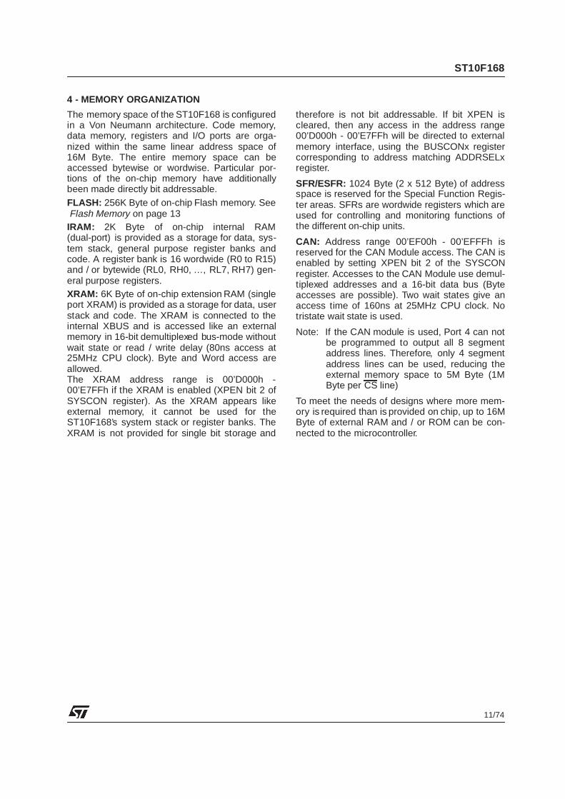
The memory space of the ST10F168 is configuredin a Von Neumann architecture. Code memory,data memory, registers and I/O ports are orga-nized within the same linear address space of16M Byte. The entire memory space can beaccessed bytewise or wordwise. Particular por-tions of the on-chip memory have additionallybeen made directly bit addressable.FLASH: 256K Byte of on-chip Flash memory. SeeFlash Memory on page 13IRAM: 2K Byte of on-chip internal RAM(dual-port) is provided as a storage for data, sys-tem stack, general purpose register banks andcode. A register bank is 16 wordwide (R0 to R15)and / or bytewide (RL0, RH0, …, RL7, RH7) gen-eral purpose registers.XRAM: 6K Byte of on-chip extension RAM (singleport XRAM) is provided as a storage for data, userstack and code. The XRAM is connected to theinternal XBUS and is accessed like an externalmemory in 16-bit demultiplexed bus-mode withoutwait state or read / write delay (80ns access at25MHz CPU clock). Byte and Word access areallowed.The XRAM address range is 00’D000h -00’E7FFh if the XRAM is enabled (XPEN bit 2 ofSYSCON register). As the XRAM appears likeexternal memory, it cannot be used for theST10F168’s system stack or register banks. TheXRAM is not provided for single bit storage and
therefore is not bit addressable. If bit XPEN iscleared, then any access in the address range00’D000h - 00’E7FFh will be directed to externalmemory interface, using the BUSCONx registercorresponding to address matching ADDRSELxregister.
SFR/ESFR: 1024 Byte (2 x 512 Byte) of addressspace is reserved for the Special Function Regis-ter areas. SFRs are wordwide registers which areused for controlling and monitoring functions ofthe different on-chip units.
CAN: Address range 00’EF00h - 00’EFFFh isreserved for the CAN Module access. The CAN isenabled by setting XPEN bit 2 of the SYSCONregister. Accesses to the CAN Module use demul-tiplexed addresses and a 16-bit data bus (Byteaccesses are possible). Two wait states give anaccess time of 160ns at 25MHz CPU clock. Notristate wait state is used.
Note: If the CAN module is used, Port 4 can notbe programmed to output all 8 segmentaddress lines. Therefore, only 4 segmentaddress lines can be used, reducing theexternal memory space to 5M Byte (1MByte per CS line)
To meet the needs of designs where more mem-ory is required than is provided on chip, up to 16MByte of external RAM and / or ROM can be con-nected to the microcontroller.

ST10F168
12/74
Figure 4 : ST10F168 on-chip memory mapping
0x5’00000x14
0x4’FFFF0x4’C0000x13
0x4’80000x12
0x4’40000x11
0x4’00000x10
0x3’C0000x0F
0x3’80000x0E
Bank 3 : 96K Byte
0x3’7FFF
0x3’40000x0D
0x3’00000x0C
0x2’C0000x0B
0x2’80000x0A
0x2’40000x09
0x2’00000x08
Bank 2 : 96K Byte
0x1’FFFF0x1’C0000x07
0x1’80000x06
Bank 1H : 32K Byte
Bank 1L : 16K Byte0x1’40000x05
0x04Bank 0 : 16K Byte
0x1’0000
Bank 1L : 16K Byte0x0’40000x01
0x00Bank 0 : 16K Byte
0x0’0000
0x02 0x0’8000
0x0’FFFF
SFR Area
0x0’FE00
0x0’FDFF
IRAM : 2K Byte
0x0’F600
0x0’EFFF
CAN Module
0x0’EF00
0x0’E7FF
XRAM : 6K Byte
0x0’D000
* Bank 0 and Bank 1 L may be remapped from segment 0to segment 1 by setting SYSCON.ROMS1 (before EINIT)
RAM, SFR and X-pheripherals aremapped into the address space.SYSCON.XPEN=1 enables CANand XRAM (before EINIT)
Seg
men
t4
Seg
men
t3S
egm
ent
2S
egm
ent
1S
egm
ent
0
DataPageNumber
AbsoluteMemoryAddress
0x1’7FFF
0x1’3FFF
0x0’7FFF
0x0’3FFF
0x0’F1FF
ESFR Area
0x0’F000

ST10F168
13/74
5 - FLASH MEMORY
The ST10F168 provides 256K Byte of anelectrically erasable and reprogrammable FlashMemory on-chip.The Flash Memory can be used both for code anddata storage. It is organized into four 32-bit wideblocks allowing even double Word instructions tobe fetched in one machine cycle. The four blocksof size16K, 48K, 96K and 96K Byte can be erasedand reprogrammed individually (see Table 2 andTable 3).The Flash Memory can be programmed in a pro-gramming board or in the target system whichprovides high system flexibility. The algorithms toprogram or erase the flash memory are embed-ded in the Flash Memory itself (ST EmbeddedAlgorithm Kernel, or STEAKTM).To start a program / erase operation, the user’ssoftware has just to load GPRs with the addressand data to be programmed, or sector to beerased. STEAK uses embedded routines, which
check the validity of the programmed parameters,decode and then execute the programming orerase command. During operation, the STEAKroutines carry out checks and retries to verifyproper cell programming or erasing. When anerror occurs, STEAK returns an error-code whichidentifies the cause of the error.
A Flash Memory protection option prevents theread-back of the Flash Memory contents fromexternal memory, or from on-chip RAM. Codeoperation from within the Flash continues as nor-mal.
The first bank (16K Byte) and part of the secondbank (16K Byte out of 48K Byte) of the on-chipFlash Memory of the ST10F168 can be mappedto either segment 0 (addresses 00000h to07FFFh) or to segment 1 (addresses 10000h to17FFFh) during the initialization phase. Externalmemory can be used for additional systemflexibility.
VDD = 5V ± 10%, VPP = 12V ± 5%, VSS = 0V, fCPU = 25MHz, for Q6 version : TA = -40°C, +85°C and forQ3 version TA = -40°C, + 125°C.
Table 2 : Flash Memory Characteristics
Symbol Parameter Test Conditions Min. Typ. Max. Unit
fCPU CPU Frequency duringerasing / programming operation
5 - 32 MHz
Cyc Erasing / Programming Cycles fCPU = 25MHz - - 10K
tSPRG Single Word Programming Time fCPU = 25MHz - 40 1500 µs
tDPRG Double Word Programming Time fCPU = 25MHz - 40 1500 µs
tEBNK Sector Erasing Time fCPU = 25MHz - 3 15 s
tRET Data Retention Time Defectivity below 1ppm / year 20 - - year
Table 3 : Flash Memory Bank Organisation
Bank Addresses (segment 0) Addresses (segment 1) Size (Byte)
0
1
2
3
000000h to 003FFFh
004000h to 007FFFh + 018000h to 01FFFFh
020000h to 037FFFh
038000h to 04FFFFh
010000h to 013FFFh
014000h to 01FFFFh
020000h to 03FFFFh
038000h to 04FFFFh
16K
48K
96K
96K

ST10F168
14/74
5.1 - Programming / Erasing with STEmbedded Algorithm KernelThere are three stages to run STEAK :– To load the registers R0 to R4 with the STEAK
command, the address and the data to be pro-gramed, or sector to be erased. Table 4 givesthe STEAK parameters for each type of Flashprogramming / erasing operation. Table 5 de-fines the codes used in Table 4.
– To initiate the Unlock Sequence. The Unlock Se-quence is composed of two consecutive writesto an even address in the Flash active addressspace - the first write has direct addressingmode (MOV mem, Rwn) - the second write hasindirect addressing mode (MOV [Rwm], Rwn).Rwn can be any unused Word-GPR (R6 to R15)loaded with a value resulting in the same evenaddress as “mem”.
– To read the return values in R0. When the em-bedded programming / erasing algorithm returnsto trigger point, return values are given in R0.Table 6 gives the error-code definitions, Table 7gives the return values in each register for eachtype of Flash programming / erasing command.
Note: The Flash Embedded STEAK Algorithmsrequire at least 50 words on the InternalSystem Stack. STEAK verifies that there isenough free space on the System Stack,before performing a programming or eras-ing operation.The MDH, MDL and MDCregister content are modified.
Code examples for programming and erasing theFlash Memory using STEAK are given inSection 5.2.Note For more details refer to STEAK applica-
tion note on www.st.com web site.
Table 4 : STEAK parameters
Command R0 R1 R2 R3 R4
Single Word programming 55Ash AddOff W nu 2TCL
Double Word programming DD4sh AddOff DWL DWH 2TCL
Multiple (block) programming AA5sh BegAddOff EndAddOff SourceAddr 2TCL
Sector Erasing EEEEh 5555h Bnk Bnk 2TCL
Set Flash Protection UPROG bit CCCCh 5555h 3333h AAAAh 2TCL
Read Status 7777h nu nu nu 2TCL
Table 5 : Programming / erasing code definition
s Segment of the Target Flash Memory cell,
AddOff Segment Offset of the Target Flash Memory cell. Must be even value (Word-aligned address).
W Data (Word) to be written in Flash.
DWL,DWH Data (double Word, DHL = low Word, DWH = high Word) to be written in Flash.
BegAddOffSegment Offset of the FIRST Target Flash Memory Word to be written in a Multiple programmingcommand. Must be even value (Word-aligned address).
EndAddOff
Segment Offset of the LAST Target Flash Memory Word to be written in a Multiple programmingcommand.Must be even value (Word-aligned address). The value D = (EndAddOff - BegAddOff) must be:0 <= D < 16384 (ie. up to one page (16K Byte) can be written in the flash with one multi-Wordprogramming command).
SourceAdd
Start address for the block to be programmed.This address is using implicitly the data paging mechanism of the CPU. SourceAdd value must respectthe following rules :
- SourceAdd + (EndAddOff - BegAddOff) < 16384.
- Page 0 and 1 can NOT be used for source data if bit ROMS1 = ‘1’ (in SYSCON register).
Note that source data can be located in Flash (In pages 0, 1, 6 to 19 if bit ROMS1 = ‘0’, or in pages 4 to 19if bit ROMS1 = ‘1’).
Bnk Number of the Bank to be erased. For security, R2 and R3 must hold the same value.
2TCL CPU clock period in nano-seconds (eg. R4 = 50 (32h) means CPU frequency is 20MHz).

ST10F168
15/74
Table 6 : Error Code Definition (R0 content after STEAK execution)
Note: The Flash Embedded STEAK Algorithmsrequire at least 50 words on the InternalSystem Stack for proper operation. Theprogram itself verifies that there is enoughfree space on the System Stack beforeperforming a programming or erasingoperation, by computing the Word numberbetween Stack Pointer (SP) and StackOverflow register (STKOV ).The MDH, MDL and MDC register contentare modified.Registers R0 to R4 are used as Input Datafor STEAK, and are modified as explainedabove (Return Values).
Registers R5 to R15 are used internally bySTEAK, but preserved on entry andrestore on exit of STEAK.IT IS VERY IMPORTANT TO TAKE INTOACCOUNT THE FACT THAT STEAKUSES UP TO 50 WORDS ON THE SYS-TEM STACK. TO PREVENT ANYABNORMAL SITUATION, IT IS VERYIMPORTANT TO INITIALIZE COR-RECTLY THE STACK SIZE TO AT LEAST64 WORDS, AND TO CORRECTLY INI-TIALIZE REGISTER STKOV.
Error Code Meaning
00h Operation was successful
01h Flash Protection is active
02h Vpp voltage not present
03h Programming operation failed
04h Address value (R1) incorrect: not in Flash address area or odd
05h CPU period out of range (must be between 30 ns to 500 ns)
06h Not enough free space on system stack for proper operation
07h Incorrect bank number (R2,R3) specified
08h Erase operation failed (phase 1)
09h Bad source address for Multiple Word programming command
0Ah Bad number of words to be copied in Multiple Word programming command: one destination will beout of flash.
0Bh PLL Unlocked or Oscillator watchdog overflow occured during programming or erasing the flash.
0Ch Erase operation failed (phase 2)
FFh Unknown or bad command
Table 7 : Return values for each programming / erase command
ProgrammingCommand R0 R1 R2 R3 R4-R15
Single ordouble Wordprogramming
Errorcode
Unchanged Data in Flash forlocation Segment +Segment Offset(R0.[3:0] with R1)
Data in Flash forlocation Segment +Segment Offset + 2(R0[3:0] with R1+2)
Unchanged
Blockprogramming
Errorcode
The last segment offset address of thelast written Word in Flash (failing Flashaddress if R0 is not equal to zero)
Undefined Unchanged
Erasing Errorcode
Undefined Unchanged
After statusread
Errorcode
Flash embedded revMSByte = major releaseLSByte = minor revision
Circuit identifiers :R2 = #0787hR3 = #0101h for this device
Unchanged

ST10F168
16/74
5.2 - Programming Examples
Programming a double Word
Note: For easier coding, the standard data paging addressing scheme is overriden for the two MOVinstructions of the Flash Trigger Sequence (EXTS instruction). However this coding also locksboth standard and PEC interrupts and class A hardware traps. This override can be replaced byan ATOMIC instruction if the standard DPP addressing scheme must be preserved.
; code shown below assumes that Flash is mapped in segment 1
; ie. bit ROMS1 = ‘1’ in SYSCON register
; Flash must be enabled, ie. bit ROMEN = ‘1’ in SYSCON.
MOV R0, #0DD40h ; DD4xh : Double Word programming command
OR R0, #01h ; Selects segment 1 in flash memory
MOV R1, #00224h ; Address to be programmed is 01’0224h
MOV R2, #03456h ; Data to be programmed at 01’0224h
MOV R3, #04567h ; Data to be programmed at 01’0226h
MOV R4, #050d ; 50ns is 20MHz CPU clock frequency
MOV R7, #08000h ; R7 used for Flash trigger sequence
#define FCR 08000h
; Flash Unlock Sequence consists in two consecutive writes, with the directaddressing mode and then the indirect addressing mode. FCR must represent aneven address in the active address space of the Flash memory, and Rwn can beany unused Word GPR (R6 to R15)loaded with a value resulting in the same evenaddress than FCR
EXTS #1, #2 ; Flash can be mapped in segment 0 or 1
MOV FCR, R7 ; first part
MOV [R7], R7 ; second part
NOP ; WARNING: place 2 NOP operations after
NOP ; the Unlock sequence to avoid all possible
; pipeline conflicts in STEAK programs

ST10F168
17/74
Programming a block of dataThe following code is provided as an example to program a block of data. Flash to be programmed is fromaddress 01’9000h to 01’9FFEh (included). Source data (data to be copied into flash) is located in externalRAM from address 05’1000h (to 05’1FFEh, implicitly) :
; code shown below assumes that flash is mapped in segment 1
; ie. bit ROMS1 = ‘1’ in SYSCON register
; Flash must be enabled, ie. bit ROMEN = ‘1’ in SYSCON.
MOV R0, #0AA50h ; AA5xh : Multi Word programming command
OR R0, #01h ; Selects segment 1 in Flash memory
MOV R1, #09000h ; First Flash Segment Offset Address
MOV R2, #09FFEh ; Last Flash Segment Offset Address
MOV R3, #09000h ; Source data address: use DPP2 as
; data page pointer
SCXT DPP2,#20d ; Source is in page 20 (first page of
; segment 5): save previous DPP2 value
; and load it with source page number
MOV R4, #050d ; 50ns is 20MHz CPU clock frequency
MOV R7, #08000h ; R7 used for Flash trigger sequence
#define FCR 08000h
EXTS #1, #2 ; Flash can be mapped in segment 0 or 1
MOV FCR, R7 ; first part
MOV [R7], R7 ; second part
NOP ; WARNING: place 2 NOP operations after
NOP ; the Unlock sequence to avoid all possible
; pipeline conflicts in STEAK programs
POP DPP2 ; restore DPP2

ST10F168
18/74
5.3 - Flash Memory Configuration
The default memory configuration of theST10F168 Memory is determined by the state ofthe EA pin at reset. This value is stored in theInternal ROM Enable bit : ROMEN of theSYSCON Register.
When ROMEN = 0, the internal FLASH is disabledand external ROM is used for startup control.Flash memory can be enabled later by setting theROMEN bit of SYSCON to 1. Ensure that thecode which performs this setting is NOT runningfrom external ROM in a segment that will bereplaced by FLASH memory, otherwise unex-pected behaviour may occur.
For example, if the external ROM code is locatedin the first 32K Byte of segment 0, the first32K Byte of the FLASH must then be enabled insegment 1. This is done by setting the ROMS1 bitof SYSCON to 0, before or simultaneously withsetting the ROMEN bit. This must be done in theexternally supplied program, before the executionof the EINIT instruction. If program executionstarts from external memory, but the Flash mem-ory mapped in segment 0 is accessed later, thenthe code that sets the ROMEN bit must be exe-cuted either in segment 0 but above address00’8000h, or from the internal RAM.
Bit ROMS1 only affects the mapping of the first32K Byte of the Flash memory. All other parts ofthe Flash memory (addresses 01’8000h -04’FFFFh) remain unaffected.
Note: The SGTDIS Segmentation Disable /Enable must also be set to 0 to enable the use ofthe full 256K Byte of on-chip memory in additionto the external boot memory. The correct proce-dure for changing the segmentation registersmust be observed to prevent an unwanted trapcondition :
– Instructions that configure the internal memorymust only be executed from external memory orfrom the internal RAM.
– An Absolute Inter-Segment Jump (JMPS)instruction must be executed after Flash enabling,before the next instruction, even if the nextinstruction is located in the consecutive address.
– Whenever the internal memory is disabled, ena-bled or remapped, the DPPs must be explicitly(re)loaded to enable correct data accesses tothe internal memory and / or external memory.
5.4 - Flash ProtectionIf Flash Protection is active, data operands in theon-chip Flash Memory area can only be read by aprogram executed from the Flash Memory itself.
Program branches from or into the on-chip Flashmemory are possible in the Flash protectionmode. Erasing and programming of the Flashmemory is not possible as long as protection isactive.
Flash protection is controlled by the ProtectionUPROM Programming Bit (UPROG). UPROG is a’hidden’ one-time programmable bit only accessi-ble in a special mode which can be entered via aFlash EPROM programming board for example. IfUPROG is set to ”1”, Flash protection is activeafter reset. By default Flash Protection is disabled(UPROG=0).
When flash protection is active (the default afterreset if UPROG bit is set), then any read access inthe flash by a code executed from external orinternal RAM (IRAM or XRAM) will return thevalue 0B88Bh. Any call of STEAK will return theerror code ‘01’ (Protected flash).
Normally Flash protection should never be deacti-vated, once activated. If this has to be done, forexample because the Flash memory has to bereprogrammed with updated program / variables,a zero value has to be written at any even addressin the active address space of the Flash memory.This write can be done only by an instruction exe-cuted from the internal Flash Memory itself.For example:
MOV FLASH,ZEROS ; Deactivate FlashProtection.
; Flash is any even address in Flashmemory space. This instruction MUSTbe executed from Flash memory itself.
After this instruction, the flash is temporarilyde-protected, thus any read access of the flashfrom code executed from external memory orinternal RAMs will be correctly executed, and callsof STEAK can be correctly performed (program-ming, erasing or status reading).
Note: 1. That all STEAK commands re-activatethe flash protection if bit UPROG is setwhen completed.
5.5 - Bootstrap Loader Mode
Pin P0L.4 (BSL) activates the on-chip bootstraploader, when low during hardware reset. Thebootstrap loader allows moving the start code intothe internal RAM of the ST10F168 via the serialinterface ASC0. The ST10F168 will remain inbootstrap loader mode until a hardware reset withP0L.4 high or a software reset occurs. The boot-straps loader acknowledge byte is D5h.

ST10F168
19/74
6 - CENTRAL PROCESSING UNIT (CPU)
The CPU includes a 4-stage instruction pipeline, a16-bit arithmetic and logic unit (ALU) and dedi-cated SFRs. Additional hardware has been addedfor a separate multiply and divide unit, a bit-maskgenerator and a barrel shifter.
Most of the ST10F168’s instructions can be exe-cuted in one instruction cycle which requires62.5ns at 32MHz CPU clock. For example, shiftand rotate instructions are processed in oneinstruction cycle independent of the number of bitto be shifted. Multiple-cycle instructions havebeen optimized: branches are carried out in 2cycles, 16 x 16-bit multiplication in 5 cycles and a32/16 bit division in 10 cycles.The jump cachereduces the execution time of repeatedly per-formed jumps in a loop, from 2 cycles to 1 cycle.
The CPU uses a bank of 16 word registers to runthe current context. This bank of General PurposeRegisters (GPR) is physically stored within theon-chip RAM area. A Context Pointer (CP) regis-ter determines the base address of the active reg-ister bank to be accessed by the CPU. Thenumber of register banks is only restricted by theavailable internal RAM space. For easy parameterpassing, one register bank may overlap others.A system stack of up to 2048 Byte stores tempo-rary data. The system stack is allocated in theon-chip RAM area, and it is accessed by the CPUvia the stack pointer (SP) register. Two separateSFRs, STKOV and STKUN, are implicitly com-pared against the stack pointer value on eachstack access, for the detection of a stack overflowor underflow.
Figure 5 : CPU Block Diagram
32
InternalRAM
2K Byte
GeneralPurposeRegisters
R0
R15MDHMLD
Barrel-Shift
Mul./Div.-HWBit-Mask Gen.
ALU
16-Bit
CP
SPSTKOVSTKUN
Exec. UnitInstr. PtrInstr. Reg
4-StagePipeline
PSWSYSCON
BUSCON 0BUSCON 1BUSCON 2BUSCON 3BUSCON 4
ADDRSEL 1ADDRSEL 2ADDRSEL 3ADDRSEL 4
Data Pg. Ptrs Code Seg. Ptr.
CPU
256K Byte
Flash
memory
16
16
Bankn
Banki
Bank0

ST10F168
20/74
6.1 - Instruction Set SummaryThe Table 8 lists the instructions of the ST10F168.The various addressing modes, instruction opera-tion, parameters for conditional execution of
instructions, opcodes and a detailed description ofeach instruction can be found in the “ST10 FamilyProgramming Manual”.
Table 8 : Instruction set summary
Mnemonic Description Bytes
ADD(B) Add Word (Byte) operands 2 / 4
ADDC(B) Add Word (Byte) operands with Carry 2 / 4
SUB(B) Subtract Word (Byte) operands 2 / 4
SUBC(B) Subtract Word (Byte) operands with Carry 2 / 4
MUL(U) (Un)Signed multiply direct GPR by direct GPR (16 x 16-bit) 2
DIV(U) (Un)Signed divide register MDL by direct GPR (16 / 16-bit) 2
DIVL(U) (Un)Signed long divide register MD by direct GPR (32 / 16-bit) 2
CPL(B) Complement direct Word (Byte) GPR 2
NEG(B) Negate direct Word (Byte) GPR 2
AND(B) Bitwise AND, (Word / Byte operands) 2 / 4
OR(B) Bitwise OR, (Word / Byte operands) 2 / 4
XOR(B) Bitwise XOR, (Word / Byte operands) 2 / 4
BCLR Clear direct bit 2
BSET Set direct bit 2
BMOV(N) Move (negated) direct bit to direct bit 4
BAND, BOR, BXOR AND / OR / XOR direct bit with direct bit 4
BCMP Compare direct bit to direct bit 4
BFLDH/L Bitwise modify masked high / low Byte of bit-addressable direct Word memory withimmediate data
4
CMP(B) Compare Word (Byte) operands 2 / 4
CMPD1/2 Compare Word data to GPR and decrement GPR by 1/2 2 / 4
CMPI1/2 Compare Word data to GPR and increment GPR by 1/2 2 / 4
PRIOR Determine number of shift cycles to normalize direct Word GPR and store result indirect Word GPR
2
SHL/SHR Shift left / right direct Word GPR 2
ROL/ROR Rotate left / right direct Word GPR 2
ASHR Arithmetic (sign bit) shift right direct Word GPR 2
MOV(B) Move Word (Byte) data 2 / 4
MOVBS Move Byte operand to Word operand with sign extension 2 / 4
MOVBZ Move Byte operand to Word operand. with zero extension 2 / 4
JMPA, JMPI, JMPR Jump absolute / indirect / relative if condition is met 4
JMPS Jump absolute to a code segment 4
J(N)B Jump relative if direct bit is (not) set 4
JBC Jump relative and clear bit if direct bit is set 4

ST10F168
21/74
JNBS Jump relative and set bit if direct bit is not set 4
CALLA, CALLI, CALLR Call absolute / indirect / relative subroutine if condition is met 4
CALLS Call absolute subroutine in any code segment 4
PCALL Push direct Word register onto system stack and call absolute subroutine 4
TRAP Call interrupt service routine via immediate trap number 2
PUSH, POP Push / pop direct Word register onto / from system stack 2
SCXT Push direct Word register onto system stack and update register with Word operand 4
RET Return from intra-segment subroutine 2
RETS Return from inter-segment subroutine 2
RETP Return from intra-segment subroutine and pop direct Word register from systemstack
2
RETI Return from interrupt service subroutine 2
SRST Software Reset 4
IDLE Enter Idle Mode 4
PWRDN Enter Power Down Mode (supposes NMI-pin being low) 4
SRVWDT Service Watchdog Timer 4
DISWDT Disable Watchdog Timer 4
EINIT Signify End-of-Initialization on RSTOUT-pin 4
ATOMIC Begin ATOMIC sequence 2
EXTR Begin EXTended Register sequence 2
EXTP(R) Begin EXTended Page (and Register) sequence 2 / 4
EXTS(R) Begin EXTended Segment (and Register) sequence 2 / 4
NOP Null operation 2
Table 8 : Instruction set summary
Mnemonic Description Bytes

ST10F168
22/74
7 - EXTERNAL BUS CONTROLLER
All external memory accesses are performed bythe on-chip external bus controller. The EBC canbe programmed to single chip mode when noexternal memory is required, or to one of four dif-ferent external memory access modes :– 16 / 18 / 20 / 24-bit addresses and 16-bit data,
demultiplexed.– 16 / 18 / 20 / 24-bit addresses and 16-bit data,
multiplexed.– 16 / 18 / 20 / 24-bit addresses and 8-bit data,
multiplexed.– 16 / 18 / 20 / 24-bit addresses and 8-bit data,
demultiplexed.In demultiplexed bus modes addresses are outputon Port1 and data are input / output on Port0 orP0L, respectively. In the multiplexed bus modesboth addresses and data use Port0 for input / out-put.Timing characteristics of the external bus inter-face (memory cycle time, memory tri-state time,length of ALE and read / write delay) are program-mable giving the choice of a wide range of memo-ries and external peripherals. Up to 4 independentaddress windows may be defined (using registerpairs ADDRSELx / BUSCONx) to access differentresources and bus characteristics. These addresswindows are arranged hierarchically whereBUSCON4 overrides BUSCON3 and BUSCON2overrides BUSCON1. All accesses to locationsnot covered by these 4 address windows are con-trolled by BUSCON0. Up to 5 external CS signals(4 windows plus default) can be generated in
order to save external glue logic. Access to veryslow memories is supported by a ‘Ready’ function.
A HOLD/HLDA protocol is available for bus arbi-tration which shares external resources with otherbus masters. The bus arbitration is enabled bysetting bit HLDEN in register SYSCON. After set-ting HLDEN once, pins P6.7...P6.5 (BREQ,HLDA, HOLD) are automatically controlled by theEBC. In master mode (default after reset) theHLDA pin is an output. By setting bit DP6.7 to’1’the slave mode is selected where pin HLDA isswitched to input. This directly connects the slavecontroller to another master controller withoutglue logic.
For applications which require less externalmemory space, the address space can berestricted to 1M Byte, 256K Byte or to 64K Byte.Port4 outputs all 8 address lines if an addressspace of 16M Byte is used, otherwise four, two orno address lines.
Chip select timing can be programmed. By default(after reset), the CSx lines change half a CPUclock cycle after the rising edge of ALE. With theCSCFG bit set in the SYSCON register the CSxlines can change with the rising edge of ALE.
The active level of the READY pin can be set bybit RDYPOLx in the BUSCONx registers. Whenthe READY function is enabled for a specificaddress window, each bus cycle within the win-dow must be terminated with the active leveldefined by bit RDYPOLx in the associated BUS-CONx register.

ST10F168
23/74
8 - INTERRUPT SYSTEM
The interrupt response time for internal programexecution is from 157ns to 375ns at 32MHz CPUclock.The ST10F168 architecture supports severalmechanisms for fast and flexible response to ser-vice requests that can be generated from varioussources (internal or external) to the microcontrol-ler. Any of these interrupt requests can be ser-viced by the Interrupt Controller or by thePeripheral Event Controller (PEC).In contrast to a standard interrupt service wherethe current program execution is suspended anda branch to the interrupt vector table is performed,just one cycle is ‘stolen’ from the current CPUactivity to perform a PEC service. A PEC serviceimplies a single Byte or Word data transferbetween any two memory locations with anadditional increment of either the PEC source orthe destination pointer. An individual PEC transfercounter is implicitly decremented for each PECservice except when performing in the continuoustransfer mode. When this counter reaches zero, astandard interrupt is performed to thecorresponding source related vector location.PEC services are very well suited to perform thetransmission or the reception of blocks of data.
The ST10F168 has 8 PEC channels, each ofthem offers such fast interrupt-driven data transfercapabilities.
A interrupt control register which contains aninterrupt request flag, an interrupt enable flag andan interrupt priority bitfield is dedicated to eachexisting interrupt source. Thanks to its relatedregister, each source can be programmed to oneof sixteen interrupt priority levels. Once starting tobe processed by the CPU, an interrupt servicecan only be interrupted by a higher prioritizedservice request. For the standard interruptprocessing, each of the possible interrupt sourceshas a dedicated vector location.
Fast external interrupt inputs are provided to ser-vice external interrupts with high precisionrequirements. These fast interrupt inputs featureprogrammable edge detection (rising edge, fallingedge or both edges). Software interrupts are sup-ported by means of the ‘TRAP’ instruction in com-bination with an individual trap (interrupt) number.Table 9 shows all the available ST10F168 inter-rupt sources and the corresponding hard-ware-related interrupt flags, vectors, vectorlocations and trap (interrupt) numbers:
Table 9 : Interrupt sources
Source of Interrupt or PEC Service Request RequestFlag
EnableFlag
InterruptVector
VectorLocation
TrapNumber
CAPCOM Register 0 CC0IR CC0IE CC0INT 00’0040h 10h
CAPCOM Register 1 CC1IR CC1IE CC1INT 00’0044h 11h
CAPCOM Register 2 CC2IR CC2IE CC2INT 00’0048h 12h
CAPCOM Register 3 CC3IR CC3IE CC3INT 00’004Ch 13h
CAPCOM Register 4 CC4IR CC4IE CC4INT 00’0050h 14h
CAPCOM Register 5 CC5IR CC5IE CC5INT 00’0054h 15h
CAPCOM Register 6 CC6IR CC6IE CC6INT 00’0058h 16h
CAPCOM Register 7 CC7IR CC7IE CC7INT 00’005Ch 17h
CAPCOM Register 8 CC8IR CC8IE CC8INT 00’0060h 18h
CAPCOM Register 9 CC9IR CC9IE CC9INT 00’0064h 19h
CAPCOM Register 10 CC10IR CC10IE CC10INT 00’0068h 1Ah
CAPCOM Register 11 CC11IR CC11IE CC11INT 00’006Ch 1Bh
CAPCOM Register 12 CC12IR CC12IE CC12INT 00’0070h 1Ch
CAPCOM Register 13 CC13IR CC13IE CC13INT 00’0074h 1Dh
CAPCOM Register 14 CC14IR CC14IE CC14INT 00’0078h 1Eh
CAPCOM Register 15 CC15IR CC15IE CC15INT 00’007Ch 1Fh
CAPCOM Register 16 CC16IR CC16IE CC16INT 00’00C0h 30h
CAPCOM Register 17 CC17IR CC17IE CC17INT 00’00C4h 31h

ST10F168
24/74
CAPCOM Register 18 CC18IR CC18IE CC18INT 00’00C8h 32h
CAPCOM Register 19 CC19IR CC19IE CC19INT 00’00CCh 33h
CAPCOM Register 20 CC20IR CC20IE CC20INT 00’00D0h 34h
CAPCOM Register 21 CC21IR CC21IE CC21INT 00’00D4h 35h
CAPCOM Register 22 CC22IR CC22IE CC22INT 00’00D8h 36h
CAPCOM Register 23 CC23IR CC23IE CC23INT 00’00DCh 37h
CAPCOM Register 24 CC24IR CC24IE CC24INT 00’00E0h 38h
CAPCOM Register 25 CC25IR CC25IE CC25INT 00’00E4h 39h
CAPCOM Register 26 CC26IR CC26IE CC26INT 00’00E8h 3Ah
CAPCOM Register 27 CC27IR CC27IE CC27INT 00’00ECh 3Bh
CAPCOM Register 28 CC28IR CC28IE CC28INT 00’00F0h 3Ch
CAPCOM Register 29 CC29IR CC29IE CC29INT 00’0110h 44h
CAPCOM Register 30 CC30IR CC30IE CC30INT 00’0114h 45h
CAPCOM Register 31 CC31IR CC31IE CC31INT 00’0118h 46h
CAPCOM Timer 0 T0IR T0IE T0INT 00’0080h 20h
CAPCOM Timer 1 T1IR T1IE T1INT 00’0084h 21h
CAPCOM Timer 7 T7IR T7IE T7INT 00’00F4h 3Dh
CAPCOM Timer 8 T8IR T8IE T8INT 00’00F8h 3Eh
GPT1 Timer 2 T2IR T2IE T2INT 00’0088h 22h
GPT1 Timer 3 T3IR T3IE T3INT 00’008Ch 23h
GPT1 Timer 4 T4IR T4IE T4INT 00’0090h 24h
GPT2 Timer 5 T5IR T5IE T5INT 00’0094h 25h
GPT2 Timer 6 T6IR T6IE T6INT 00’0098h 26h
GPT2 CAPREL Register CRIR CRIE CRINT 00’009Ch 27h
A/D Conversion Complete ADCIR ADCIE ADCINT 00’00A0h 28h
A/D Overrun Error ADEIR ADEIE ADEINT 00’00A4h 29h
ASC0 Transmitter S0TIR S0TIE S0TINT 00’00A8h 2Ah
ASC0 Transmitter Buffer S0TBIR S0TBIE S0TBINT 00’011Ch 47h
ASC0 Receiver S0RIR S0RIE S0RINT 00’00ACh 2Bh
ASC0 Error S0EIR S0EIE S0EINT 00’00B0h 2Ch
SSC Transmitter SCTIR SCTIE SCTINT 00’00B4h 2Dh
SSC Receiver SCRIR SCRIE SCRINT 00’00B8h 2Eh
SSC Error SCEIR SCEIE SCEINT 00’00BCh 2Fh
PWM Channel 0...3 PWMIR PWMIE PWMINT 00’00FCh 3Fh
CAN Interface XP0IR XP0IE XP0INT 00’0100h 40h
X-Peripheral Node XP1IR XP1IE XP1INT 00’0104h 41h
X-Peripheral Node XP2IR XP2IE XP2INT 00’0108h 42h
PLL Unlock XP3IR XP3IE XP3INT 00’010Ch 43h
Table 9 : Interrupt sources (continued)
Source of Interrupt or PEC Service Request RequestFlag
EnableFlag
InterruptVector
VectorLocation
TrapNumber

ST10F168
25/74
Hardware traps are exceptions or error conditionsthat arise during run-time. They cause immediatenon-maskable system reaction similar to a stan-dard interrupt service (branching to a dedicatedvector table location).The occurrence of a hardware trap isadditionally signif ied by an individual bit in thetrap flag register (TFR). Except when another
higher prioritized trap service is in progress, ahardware trap will interrupt any other programexecution.
Hardware trap services cannot not be interruptedby standard interrupt or by PEC interrupts.
Table 10 shows all of the possible exceptions orerror conditions that can arise during run-time :
Table 10 : Exceptions or error conditions that can arise during run-time
Exception Condit ion Trap Flag Trap Vector Vector Location Trap Number Trap Priority
Reset Functions
Hardware Reset RESET 00’0000h 00h III
Software Reset RESET 00’0000h 00h III
Watchdog Timer Overflow RESET 00’0000h 00h III
Class A Hardware Traps
Non-Maskable Interrupt NMI NMITRAP 00’0008h 02h II
Stack Overflow STKOF STOTRAP 00’0010h 04h II
Stack Underflow STKUF STUTRAP 00’0018h 06h II
Class B Hardware Traps
Undefined Opcode UNDOPC BTRAP 00’0028h 0Ah I
Protected Instruction Fault PRTFLT BTRAP 00’0028h 0Ah I
Illegal Word Operand Access ILLOPA BTRAP 00’0028h 0Ah I
Illegal Instruction Access ILLINA BTRAP 00’0028h 0Ah I
Illegal External Bus Access ILLBUS BTRAP 00’0028h 0Ah I
Reserved [2Ch –3Ch] [0Bh – 0Fh]
Software TrapsTRAP Instruction
Any [00’0000h– 00’01FCh]in steps of 4h
Any [00h – 7Fh] Current CPUPriority

ST10F168
26/74
9 - CAPTURE / COMPARE (CAPCOM) UNIT
The ST10F168 has two 16 channel CAPCOMunits which support generation and control oftiming sequences on up to 32 channels with amaximum resolution of 320ns at 32MHz CPUclock.The CAPCOM units are typically used to handlehigh speed I/O tasks such as pulse and waveformgeneration, pulse width modulation (PMW), Digitalto Analog (D/A) conversion, software timing, ortime recording relative to external events.Four 16-bit timers (T0/T1, T7/T8) with reloadregisters provide two independent time bases forthe capture / compare register array.The input clock for the timers is programmable toseveral prescaled values of the internal systemclock, or may be derived from an overflow / under-flow of timer T6 in module GPT2.This provides a wide range of variation for thetimer period and resolution and allows preciseadjustments to application specific requirements.In addition, external count inputs for CAPCOMtimers T0 and T7 allow event scheduling for thecapture / compare registers relative to externalevents.Each of the two capture / compare register arrayscontain 16 dual purpose capture / compare regis-ters, each of which may be individually allocatedto either CAPCOM timer T0 or T1 (T7 or T8,respectively), and programmed for captureor compare functions. Each register has oneassociated port pin which serves as an input pinfor triggering the capture function, or as an output
pin (except for CC24...CC27) to indicate theoccurrence of a compare event.
When a capture / compare register has beenselected for capture mode, the current contents ofthe allocated timer will be latched (captured) intothe dedicated capture / compare register inresponse to an external event at thecorresponding port pin which is associated withthis register. In addition, a specific interruptrequest for this capture / compare register isgenerated.
Either a positive, a negative, or both a positiveand a negative external signal transition at the pincan be selected as the triggering event.
The contents of all the registers which have beenselected for one of the five compare modes arecontinuously compared with the contents of theallocated timers.
When a match occurs between the timer valueand the value in a capture / compare register, spe-cific actions will be taken based on the selectedcompare mode.
The input frequencies fTx, for the timer inputselector Txl, are determined as a function of theCPU clock. The timer input frequencies, the reso-lution and the periods which result from theselected pre-scaler option in TxI when using a25MHz CPU clock are listed in the Table 12.
The numbers of the timer periods are based on areload value of 0000h. Note that some numbersare rounded to 3 significant figures.
Table 11 : Compare Modes
Compare Modes Function
Mode 0 Interrupt-only compare mode ; several compare interrupts per timer period are possible.
Mode 1 Pin toggles on each compare match ; several compare events per timer period are possible.
Mode 2 Interrupt-only compare mode ; only one compare interrupt per timer period is generated.
Mode 3 Pin set ‘1’ on match; pin reset ‘0’ on compare time overflow ; only one compare event pertimer period is generated.
Double Register Mode Two registers operate on one pin; pin toggles on each compare match ; several compareevents per timer period are possible.

ST10F168
27/74
Table 12 : CAPCOM timer input frequencies, resolution and periods
Note: 1. Input only.
fCPU = 25MHzTimer Input Selection TxI
000b 001b 010b 011b 100b 101b 110b 111b
fCPU pre-scaler 8 16 32 64 128 256 512 1024
Input Frequency 3.125MHz 1.56MHz 781KHz 391KHz 195KHz 97.7KHz 48.8KHz 24.4KHz
Resolution 320ns 640ns 1.28µs 2.56µs 5.12µs 10.24µs 20.48µs 40.96µs
Period 21.0ms 41.9ms 83.9ms 167ms 336ms 671ms 1.34s 2.68s
Table 13 : CAPCOM Channels Pin Assignement
CAPCOMUnit Channel 0 1 2 3 4 5 6 7 8 9 10 11 12 13 14 15
CAPCOM1 I/O CC0 CC1 CC2 CC3 CC4 CC5 CC6 CC7 CC81 CC91 CC101 CC111 CC12 CC13 CC14 CC15
Port 2.0 2.1 2.2 2.3 2.4 2.5 2.6 2.7 2.8 2.9 2.10 2.11 2.12 2.13 2.14 2.15
Pin Number 47 48 49 50 51 52 53 54 57 58 59 60 61 62 63 64
CAPCOM2 I/O CC16 CC17 CC18 CC19 CC20 CC21 CC22 CC23 CC24 CC25 CC26 CC27 CC28 CC29 CC30 CC31
Port 8.0 8.1 8.2 8.3 8.4 8.5 8.6 8.7 1H.4 1H.5 1H.6 1H.7 7.4 7.5 7.6 7.7
Pin Number 9 10 11 12 13 14 15 16 132 133 134 135 23 24 25 26

ST10F168
28/74
10 - GENERAL PURPOSE TIMER UNIT
The GPT unit is a flexible multifunctional timer /counter structure which is used for time relatedtasks such as event timing and counting, pulsewidth and duty cycle measurements, pulsegeneration, or pulse multiplication. The GPT unitcontains five 16-bit timers organized into twoseparate modules GPT1 and GPT2. Each timerin each module may operate independently inseveral different modes, or may be concatenatedwith another timer of the same module.
10.1 - GPT1Each of the three timers T2, T3, T4 of the GPT1module can be configured individually for one offour basic modes of operation: timer , gatedtimer , counter mode and incremental interfacemode. In timer mode, the input clock for a timer isderived from the CPU clock, divided by a pro-grammable prescaler. In counter mode, the timer isclocked in reference to external events. Pulse widthor duty cycle measurement is supported in gatedtimer mode where the operation of a timer is con-trolled by the ‘gate’ level on an external input pin.For these purposes, each timer has one associatedport pin (TxIN) which serves as gate or clock input.Table 14 lists the timer input frequencies, resolu-tion and periods for each pre-scaler option at25MHz CPU clock. This also applies to the GatedTimer Mode of T3 and to the auxiliary timers T2and T4 in Timer and Gated Timer Mode.The count direction (up / down) for each timer isprogrammable by software or may be altereddynamically by an external signal on a port pin(TxEUD).In Incremental Interface Mode, the GPT1 timers(T2, T3, T4) can be connected directly to theincremental position sensor signals A and B bytheir respective inputs TxIN and TxEUD. Directionand count signals are internally derived fromthese two input signals so that the contents of the
respective timer Tx corresponds to the sensorposition. The third position sensor signal TOP0can be connected to an interrupt input.Timer T3 has output toggle latches (TxOTL) whichchanges state on each timer over-flow / under-flow. The state of this latch may be output on portpins (TxOUT) e. g. for time out monitoring ofexternal hardware components, or may be usedinternally to clock timers T2 and T4 for high reso-lution of long duration measurements.In addition to their basic operating modes, timersT2 and T4 may be configured as reload or captureregisters for timer T3. When used as capture orreload registers, timers T2 and T4 are stopped.The contents of timer T3 is captured into T2 or T4in response to a signal at their associated inputpins (TxIN). Timer T3 is reloaded with thecontents of T2 or T4 triggered either by anexternal signal or by a selectable state transitionof its toggle latch T3OTL. When both T2 and T4are configured to alternately reload T3 onopposite state transitions of T3OTL with the lowand high times of a PWM signal, this signalcan be constantly generated without softwareintervention.
10.2 - GPT2The GPT2 module provides precise event controland time measurement. It includes two timers (T5,T6) and a capture / reload register (CAPREL).Both timers can be clocked with an input clockwhich is derived from the CPU clock via a pro-grammable prescaler or with external signals. Thecount direction (up / down) for each timer is pro-grammable by software or may additionally bealtered dynamically by an external signal on a portpin (TxEUD). Concatenation of the timers is sup-ported via the output toggle latch (T6OTL) of timerT6 which changes its state on each timeroverflow / underflow.
Table 14 : GPT1 timer input frequencies, resolution and periods
fCPU = 25MHzTimer Input Selection T2I / T3I / T4I
000b 001b 010b 011b 100b 101b 110b 111b
Pre-scaler Factor 8 16 32 64 128 256 512 1024
Input Frequency 3.125MHz 1.563MHz 781.3MHz 390KHz 195.3KHz 97.66KHz 48.83KHz 24.41KHz
Resolution 320ns 640ns 1.28µs 2.56µs 5.12µs 10.24µs 20.48µs 40.96µs
Period 21.0ms 41.9ms 83.9ms 167ms 336ms 671ms 1.34s 2.68s

ST10F168
29/74
The state of this latch may be used to clock timerT5, or it may be output on a port pin (T6OUT).The overflows / underflows of timer T6 can also beused to clock the CAPCOM timers T0 or T1, andto cause a reload from the CAPREL register.The CAPREL register can capture the contents ofT5 from an external signal transition on thecorresponding port pin (CAPIN), and T5 may beoptionally cleared after the capture procedure.This allows absolute time differences to bemeasured or pulse multiplication to be performedwithout software overhead.
The capture trigger (timer T5 to CAPREL) mayalso be generated on transitions of GPT1 timer T3inputs T3IN and / or T3EUD. This is useful whenT3 operates in Incremental Interface Mode.
Table 15 GPT2 timer input frequencies, resolutionand periods lists the timer input frequencies, reso-lution and periods for each pre-scaler option at25MHz CPU clock. This also applies to the GatedTimer Mode of T6 and to the auxiliary timer T5 inTimer and Gated Timer Mode.
Table 15 : GPT2 timer input frequencies, resolution and periods
fCPU = 25MHzTimer Input Selection T5I / T6I
000b 001b 010b 011b 100b 101b 110b 111b
Pre-scaler Factor 4 8 16 32 64 128 256 512
Input Frequency 6.25MHz 3.125MHz 1.563MHz 781.3KHz 390KHz 195.3KHz 97.66KHz 48.83KHz
Resolution 160ns 320ns 640ns 1.28µs 2.56µs 5.12µs 10.24µs 20.48µs
Period 10.49ms 21.0ms 41.9ms 83.9ms 167ms 336ms 671ms 1.34s
Figure 6 : Block Diagram of GPT1
2n n=3...10
2n n=3...10
2n n=3...10
T2EUD
T2IN
CPU Clock
CPU Clock
CPU Clock
T3EUD
T4IN
T3IN
T4EUD
T2ModeControl
T3ModeControl
T4ModeControl
GPT1 Timer T2
GPT1 Timer T3
GPT1 Timer T4
T3OTL
ReloadCapture
U/D
U/D
ReloadCapture
InterruptRequest
InterruptRequest
InterruptRequest
T3OUT
U/D

ST10F168
30/74
Figure 7 : Block Diagram of GPT2
2n n=2...9
2n n=2...9
T5EUD
T5IN
CPU Clock
CPU Clock
T6IN
T6EUD
T5ModeControl
T6ModeControl
GPT2 Timer T5
GPT2 Timer T6
U/D
InterruptRequest
U/D
T60TL
Toggle FF
T6OUT
CAPIN
Reload InterruptRequest
to CAPCOMTimers
Capture
Clear
InterruptRequest
GPT2 CAPREL

ST10F168
31/74
11 - PWM MODULE
The pulse width modulation module can generateup to four PWM output signals using edge-alignedor centre-aligned PWM. In addition, the PWMmodule can generate PWM burst signals and sin-
gle shot outputs. The Table 16 shows the PWMfrequencies for different resolutions. The level ofthe output signals is selectable and the PWMmodule can generate interrupt requests.
Table 16 : PWM unit frequencies and resolution at 25MHz CPU clock
Mode 0 Resolution 8-bit 10-bit 12-bit 14-bit 16-bit
CPU Clock / 1 40ns 97.66KHz 24.41KHz 6.104KHz 1.526KHz 0.381Hz
CPU Clock / 64 2.56µs 1.526KHz 381.5Hz 95.37Hz 23.84Hz 5.96Hz
Mode 1 Resolution 8-bit 10-bit 12-bit 14-bit 16-bit
CPU Clock / 1 40ns 48.82KHz 12.20KHz 3.05KHz 762.9Hz 190.7Hz
CPU Clock / 64 2.56µs 762.9Hz 190.7Hz 47.68Hz 11.92Hz 2.98Hz
Figure 8 : PWM Module Block Diagram
PPx Period Register
Comparator
PTx16-Bit Up/Down Counter
ShadowRegister
PWx Pulse Width Register
Input
RunControl
Clock 1
Clock 2
Comparator
*
*
*
Up/Down/Clear Control
Match
Output ControlMatch
Write Control
* User readable& writeable register
EnablePOUTx

ST10F168
32/74
12 - PARALLEL PORTS
The ST10F168 provides up to 111 I/O linesorganized into eight input / output ports and oneinput port. All port lines are bit-addressable, andall input / output lines are individually (bit-wise)programmable as input or output via directionregisters. The I/O ports are true bidirectional portswhich are switched to high impedance state whenconfigured as inputs. The output drivers of five I/Oports can be configured (pin by pin) for push-pulloperation or open-drain operation via controlregisters. During the internal reset, all port pinsare configured as inputs.The input threshold of Port 2, Port 3, Port 7 andPort 8 is selectable (TTL or CMOS-like), wherethe special CMOS-like input threshold reducesnoise sensitivity to the input hysteresis. The inputthresholds are selected with bit of PICON registerdedicated to blocks of 8 input pins (2-bit for Port2,2-bit for Port3, 1-bit for Port7, 1-bit for Port8).All pins of I/O ports also support an alternate pro-grammable function:
– Port0 and Port1 may be used as address anddata lines when accessing external memory.
– Port 2, Port 7 and Port 8 are associated with thecapture inputs or with the compare outputs ofthe CAPCOM units and / or with the outputs ofthe PWM module.
– Port 3 includes the alternate functions of timers,serial interfaces, the optional bus control signalBHE and the system clock output (CLKOUT).
– Port 4 outputs the additional segment addressbit A16 to A23 in systems where segmentationis enabled to access more than 64K Byte ofmemory.
– Port 5 is used as analog input channels of theA/D converter or as timer control signals.
– Port 6 provides optional bus arbitration signals(BREQ, HLDA, HOLD) and chip select signals.
All port lines that are not used for alternate func-tions may be used as general purpose I/O lines.

ST10F168
33/74
13 - A/D CONVERTER
A10-bit A/D converter with 16 multiplexed inputchannels and a sample and hold circuit isintegrated on-chip. The sample time (for loadingthe capacitors) and the conversion time isprogrammable and can be adjusted to theexternal circuitry.Overrun error detection / protection is controlled bythe ADDAT register. Either an interrupt request isgenerated when the result of a previous conversionhas not been read from the result register at thetime the next conversion is complete, or the nextconversion is suspended until the previous resulthas been read. For applications which require lessthan 16 analog input channels, the remaining chan-nel inputs can be used as digital input port pins.The A/D converter of the ST10F168 supports dif-ferent conversion modes :– Single channel single conversion : the analog
level of the selected channel is sampled onceand converted. The result of the conversion isstored in the ADDAT register.
– Single channel continuous conversion : theanalog level of the selected channel is repeatedlysampled and converted. The result of the conver-sion is stored in the ADDAT register.
– Auto scan single conversion : the analog levelof the selected channels are sampled once andconverted. After each conversion the result isstored in the ADDAT register. The data can betransfered to the RAM by interrupt softwaremanagement or using the powerfull PeripheralEvent Controller data transfert.
– Auto scan continuous conversion : the ana-log level of the selected channels are repeatedlysampled and converted. The result of the con-version is stored in the ADDAT register. Thedata can be transfered to the RAM by interruptsoftware management or using the powerfullPeripheral Event Controller data transfert.
– Wait for ADDAT read mode : when using con-tinuous modes, in order to avoid to overwrite
the result of the current conversion by the nextone, the ADWR bit of ADCON control registermust be activated. Then, until the ADDAT regis-ter is read, the new result is stored in a tempo-rary buffer and the conversion is on hold.
– Channel injection mode : when usingcontinuous modes, a selected channel can beconverted in between without changing thecurrent operating mode. The 10 bit data of theconversion are stored in ADRES field ofADDAT2. The current continuous mode remainsactive after the single conversion is completed.
The Table 17 ADC sample clock and conversionclock shows conversion clock and sample clock ofthe ADC unit. A complete conversion will take14tCC + 2tSC + 4TCL. This time includes the con-version it self, the sampling time and the timerequired to transfer the digital value to the resultregister. For example at 25MHz of CPU clock, theminimum complete conversion time is 7.76µs.The A/D converter provides automatic offset andlinearity self calibration. The calibration operationis performed in two ways :
– A full calibration sequence is performed after areset and lasts 1.25ms minimum (at 25MHzCPU clock). During this time, the ADBSY flag isset to indicate the operation. Normal conversioncan be performed during this time. The durationof the calibration sequence is then extended bythe time consumed by the conversions.Note : After a power-on reset, the totalunadjusted error (TUE) of the ADC might beworse than ±2LSB (max. ±4LSB). During the fullcalibration sequence, the TUE is constantlyimproved until at the end of the cycle, TUE iswithin the specified limits of ±2LSB.
– One calibration cycle is performed after eachconversion : each calibration cycle takes 4 ADCclock cycles. These operation cycles ensureconstant updating of the ADC accuracy, com-pensating changing operating conditions.
Notes: 1. See Section 20.5.5 - Direct Drive on page 55.2. tCC = TCL x 24.
Table 17 : ADC sample clock and conversion clock
ADCTCConversion Clock t CC
ADSTCSample Clock t SC
TCL1 = 1/2 x fXTAL At f CPU = 25MHz tSC = At fCPU = 25MHz
00 TCL x 24 0.48µs 00 tCC 0.48µs 2
01 Reserved, do not use Reserved 01 tCC x 2 0.96µs 2
10 TCL x 96 1.92µs 10 tCC x 4 1.92µs 2
11 TCL x 48 0.96µs 11 tCC x 8 3.84µs 2

ST10F168
34/74
14 - SERIAL CHANNELS
Serial communication with other microcontrollers,processors, terminals or external peripheral com-ponents is provided by two serial interfaces: theasynchronous / synchronous serial channel(ASC0) and the high-speed synchronous serialchannel (SSC).Two dedicated Baud rate generators set up allstandard Baud rates without the requirement ofoscillator tuning. For transmission, reception anderroneous reception, 3 separate interrupt vectorsare provided for each serial channel.
ASC0ASC0 supports full-duplex asynchronous commu-nication at up to 781.25K Baud and half-duplex
synchronous communication up to 5M Baud at25MHz system clock.
For asynchronous operation, the Baud rate gener-ator provides a clock with 16 times the rate of theestablished Baud rate.
Table 18 lists various commonly used Baud ratestogether with the required reload values and thedeviation errors compared to the intendedBaud rate.
For synchronous operation, the Baud rate genera-tor provides a clock with 4 times the rate of theestablished Baud rate.
Table 18 : Commonly used Baud rates by reload value and deviation errors
S0BRS = ‘0’, f CPU = 25MHz S0BRS = ‘1’, f CPU = 25MHz
Baud Rate (Baud) Deviation Error Reload Value Baud Rate (Baud) Deviation Error Reload Value
781 250 ±0.0% 0000h 520 833 ±0.0% 0000h
56 000 +7.3% / -0.4% 000Ch / 000Dh 56 000 +3.3% / -7.0% 0008h / 0009h
38 400 +1.7% / -3.1% 0013h / 0014h 38 400 +4.3% / -3.1% 000Ch / 000Dh
19 200 +1.7% / -0.8% 0027h / 0028h 19 200 +0.5% / -3.1% 001Ah / 001Bh
9 600 +0.5% / -0.8% 0050h/ 0051h 9 600 +0.5% / -1.4% 0035h / 0036h
4 800 +0.5% / -0.1% 00A1h / 00A2h 4 800 +0.5% / -0.5% 006Bh / 006Ch
2 400 +0.2% / -0.1% 0144h / 0145h 2 400 +0.0% / -0.5% 00D8h / 00D9h
1 200 +0.0% / -0.1% 028Ah / 028Bh 1 200 +0.0% / -0.2% 01B1h / 01B2h
600 +0.0% / -0.1% 0515h / 0516h 600 +0.0% / -0.1% 0363h / 0364h
95 +0.4% 1FFFh / 1FFFh 75 +0.0% / -0.0% 1B1Fh / 1B20h
63 +0.9% 1FFFh / 1FFFh

ST10F168
35/74
High Speed Synchronous Serial Channel (SSC)
The High-Speed Synchronous Serial InterfaceSSC provides flexible high-speed serial communi-cation between the ST10F168 and other microcon-trollers, microprocessors or external peripherals.The SSC supports full-duplex and half-duplex syn-chronous communication; The serial clock signalcan be generated by the SSC itself (master mode)or be received from an external master (slavemode). Data width, shift direction, clock polarityand phase are programmable.
This allows communication with SPI-compatibledevices. Transmission and reception of data isdouble-buffered. A 16-bit Baud rate generator pro-vides the SSC with a separate serial clock signal.The serial channel SSC has its own dedicated16-bit Baud rate generator with 16-bit reloadcapability, allowing Baud rate generation indepen-dent from the timers.
SSCBR is the dual-function Baud rate Generator /Reload register. Table 19 lists some possibleBaud rates against the required reload values andthe resulting bit times for a 25MHz CPU clock.
Note: The deviation errors given in the Table 18are rounded. To avoid deviation errors usea Baud rate crystal (providing a multiple ofthe ASC0/SSC sampling frequency).
Table 19 : Synchronous Baud rate and reloadvalues
Baud Rate Bit Time Reload Value
Reserved use areload value > 0.
--- 0000h
5M Baud 200ns 0001h
3.3M Baud 303ns 0002h
2.5M Baud 400ns 0004h
2M Baud 500ns 0005h
1M Baud 1µs 000Bh
100K Baud 10µs 007Ch
10K Baud 100µs 04E1h
1K Baud 1ms 30D3h
190.7 Baud 5.2ms FFFFh

ST10F168
36/74
15 - CAN MODULE
The integrated CAN module completely handlesthe autonomous transmission and the reception ofCAN frames according to the CAN specificationV2.0 part B (active). The on-chip CAN module canreceive and transmit standard frames with 11-bitidentifiers as well as extended frames with 29-bitidentifiers.
The CAN Module Provides full CAN functionalityon up to 15 message objects. Message object 15can be configured for basic CAN functionality.Both modes provide separate masks for accep-tance filtering, allowing a number of identifiers infull CAN mode to be accepted and disregarding anumber of identifiers in basic CAN mode. All mes-sage objects can be updated independently fromother objects and are equipped for the maximummessage length of 8 Bytes.
The bit timing is derived from the XCLK and is pro-grammable up to a data rate of 1M Baud. TheCAN module uses two pins to interface to a bustransceiver.
16 - WATCHDOG TIMER
The Watchdog Timer is a fail-safe mechanismwhich prevents the microcontroller from malfunc-tioning for long periods of time.
The Watchdog Timer is always enabled after areset of the chip and can only be disabled in the
time interval until the EINIT (end of initialization)instruction has been executed.
Therefore, the chip start-up procedure is alwaysmonitored. The software must be designed to ser-vice the watchdog timer before it overflows. If, dueto hardware or software related failures, the soft-ware fails to do so, the watchdog timer overflowsand generates an internal hardware reset. It pullsthe RSTOUT pin low in order to allow externalhardware components to be reset.
The Watchdog Timer is 16-bit, clocked with thesystem clock divided by 2 or 128. The high Byte ofthe watchdog timer register can be set to apre-specified reload value (stored in WDTREL).Each time it is serviced by the application soft-ware, the high Byte of the watchdog timer isreloaded. For security, rewrite WDTCON eachtime before the watchdog timer is serviced.
Table 20 shows the watchdog time range for25MHz CPU clock.
Table 20 : Watchdog time range (25MHz clock)
Reload valuein WDTREL
Prescaler for f CPU
2 (WDTIN = ‘0’) 128 (WDTIN = ‘1’)
FFh 20.48µs 1.31ms
00h 5.24ms 336ms

ST10F168
37/74
17 - SYSTEM RESET
System reset initializes the MCU in a predefinedstate. There are five ways to activate a reset state.The system start-up configuration is different foreach case as shown in Table 21.
17.1 - Asynchronous Reset (Long Hardware Reset)An asynchronous reset is triggered when RSTINpin is pulled low while VPP pin is at low level. Thenthe MCU is immediately forced in reset defaultstate. It pulls low RSTOUT pin, it cancels pendinginternal hold states if any, it waits for any internalaccess cycles to finish, it aborts external bus cycle,it switches buses (data, address and control sig-nals) and I/O pin drivers to high-impedance, it pullshigh Port0 pins and the reset sequence starts.
Power-on ResetThe asynchronous reset must be used during thepower-on of the MCU. Depending on crystal fre-quency, the on-chip oscillator needs about 10msto 50ms to stabilize. The logic of the MCU doesnot need a stabilized clock signal to detect anasynchronous reset, so it is suitable for power-on
conditions. To ensure a proper reset sequence,the RSTIN pin and the VPP pin must be held at lowlevel until the MCU clock signal is stabilized andthe system configuration value on Port0 is settled.
Hardware Reset
The asynchronous reset must be used to recoverfrom catastrophic situations of the application. Itmay be triggerred by the hardware of the applica-tion. Internal hardware logic and application cir-cuitry are described in Reset circuitry chapter andFigures 12, 13 and 14.
Exit of Asynchrounous Reset State
When the RSTIN pin is pulled high, the MCUrestarts. The system configuration is latched fromPort0 and ALE, RD and R/W pins are driven to theirinactive level. The MCU starts program executionfrom memory location 00’0000h in code segment 0.This starting location will typically point to the gen-eral initialization routine. Timing of asynchronousreset sequence are summarized in Figure 9.
Note: 1. RSTIN rising edge to internal latch of Port0 is 3CPU clock cycles (6 TCL) if the PLL is bypassed and the prescaler is on(fCPU = fXTAL / 2), else it is 4 CPU clock cycles (8 TCL).
Table 21 : Reset event definition
Reset Source Short-cut Conditions
Power-on reset PONR Power-on
Long Hardware reset (synchronous & asynchronous) LHWR t RSTIN > 1032 TCL
Short Hardware reset (synchronous reset) SHWR 4 TCL < t RSTIN < 1032 TCL
Watchdog Timer reset WDTR WDT overflow
Software reset SWR SRST execution
Figure 9 : Asynchronous Reset Timing
6 or 8 TCL1
CPU Clock
RSTIN
AsynchronousReset Condition
VPP
RSTOUT
ALE
Port0 Reset Configuration INST #1
InternalResetSignal
Latchingpoint of Port0for system start-upconfiguration

ST10F168
38/74
17.2 - Synchronous Reset (Warm Reset)
A synchronous reset is triggered when RSTIN pinis pulled low while VPP pin is at high level. In orderto properly activate the internal reset logic of theMCU, the RSTIN pin must be held low, at least,during 4 TCL (2 periods of CPU clock). The I/Opins are set to high impedance and RSTOUT pin isdriven low. After RSTIN level is detected, a shortduration of 12 TCL (approximately 6 periods ofCPU clock) elapes, during which pending internalhold states are cancelled and the current internalaccess cycle if any is completed. External buscycle is aborted. The internal pulldown of RSTINpin is activated if bit BDRSTEN of SYSCON reg-ister was previously set by software. This bit is
always cleared on power-on or after a resetsequence.
Exit of Synchrounous Reset StateThe internal reset sequence starts for 1024 TCL(512 periods of CPU clock) and RSTIN pin level issampled. The reset sequence is extended untilRSTIN level becomes high. Then, the MCUrestarts. The system configuration is latched fromPort0 and ALE, RD and R/W pins are driven totheir inactive level. The MCU starts program exe-cution from memory location 00’0000h in codesegment 0. This starting location will typicallypoint to the general initialization routine. Timing ofsynchronous reset sequence are summarized inFigure 10 and 11.
Notes: 1. RSTIN assertion can be released there.
2. If during the reset condition (RSTIN low), Vpp voltage drops below the threshold voltage (about 2.5V for 5V operation), theasynchronous reset is then immediately entered.
3. RSTIN rising edge to internal latch of Port0 is 3CPU clock cycles (6 TCL) if the PLL is bypassed and the prescaler is on(fCPU = fXTAL / 2), else it is 4 CPU clock cycles (8 TCL).
4) RSTIN pin is pulled low if bit BDRSTEN (bit 5 of SUSCON register) was previously set by software. Bit BDRSTEN is cleared afterreset.
Figure 10 : Synchronous Warm Reset: Short low pulse on RSTIN
CPU Clock
RSTIN
VPP
RSTOUT
ALE
Port0 INST #1
InternalResetSignal
Latchingpoint of Port0for systemstart-up configuration
6 or 8 TCL34 TCL 12 TCLmin. max.
1024 TCL
1 Internallypulled low4
Reset Configuration
2 VPP > 2.5V AsynchronousReset not entered.200µA Discharge

ST10F168
39/74
Figure 11 : Synchronous Warm Reset: Long low pulse on RSTIN
Notes: 1. RSTIN rising edge to internal latch of Port0 is 3CPUclock cycles (6 TCL) if the PLL is bypassed and theprescaler is on (fCPU = fXTAL / 2), else it is 4 CPU clockcycles (8 TCL).
2. If during the reset condition (RSTIN low), Vpp voltagedrops below the threshold voltage (about 2.5V for 5Voperation), the asynchronous reset is then immediatelyentered.
3. RSTIN pin is pulled low if bit BDRSTEN (bit 5 ofSYSCON register) was previously set by soft-ware. BitBDRSTEN is cleared after reset.
17.3 - Software ResetA software reset sequence can be triggered atany time by the protected SRST (software reset)instruction. This instruction can be deliberatelyexecuted within a program, e.g. to leave bootstraploader mode, or on a hardware trap that revealssystem failure.On execution of the SRST instruction, the internalreset sequence is started. The microcontrollerbehaviour is the same as for a synchronous reset,except that only bit P0.12...P0.8 are latched at theend of the reset sequence, while previouslylatched, bit P0.7...P0.2 are cleared.
17.4 - Watchdog Timer ResetWhen the watchdog timer is not disabled duringthe initialization, or serviced regularly during pro-gram execution, it will overflow and trigger thereset sequence.Unlike hardware and software resets, the watch-dog reset completes a running external bus cycleif this bus cycle either does not use READY, or if
READY is sampled active (low) after the pro-grammed wait states. When READY is sampledinactive (high) after the programmed wait statesthe running external bus cycle is aborted. Thenthe internal reset sequence is started.
Bit P0.12...P0.8 are latched at the end of the resetsequence and bit P0.7...P0.2 are cleared.
17.5 - Reset Circuitry
Internal reset circuitry is described in Figure 13.The RSTIN pin provides an internal pullup resistorof 50KΩ to 250KΩ (The minimum reset time mustbe calculated using the lowest value). It also pro-vides a programmable (BDRSTEN bit of SYSCONregister) pulldown to output internal reset statesignal (synchronous reset, watchdog timer resetor software reset).
This bidirectional reset function is useful in appli-cations where external devices require a reset sig-nal but cannot be connected to RSTOUT pin.
This is the case of an external memory runningcodes before EINIT ( end of initialization) instruc-tion is executed. RSTOUT pin is pulled high onlywhen EINIT is executed.
The VPP pin provides an internal weak pulldownresistor which discharges external capacitor at atypical rate of 200µA. If bit PWDCFG of SYSCONregister is set, an internal pullup resistor is acti-vated at the end of the reset sequence. This pul-lup will charge any capacitor connected on VPPpin.
CPU Clock
RSTIN
VPP
RSTOUT
ALE
Port0
InternalResetSignal
Latchingpoint of Port0for systemstart-up configuration
6 or 8 TCL14 TCL 12 TCL 1024 TCL
Internallypulled low3
Reset Configuration
2 VPP > 2.5VAsynchronousReset not entered.200µA Discharge

ST10F168
40/74
The simplest way to reset the ST10F168 is toinsert a capacitor C1 between RSTIN pin and VSS,and a capacitor between VPP pin and VSS (C0)with a pullup resistor R0 between VPP pin andVCC. The input RSTIN provides an internal pullupdevice equalling a resistor of 50kΩ to 150kΩ (theminimum reset time must be determined by thelowest value). Select C1 that produce a sufficientdischarge time to permit the internal or externaloscillator and / or internal PLL to stabilize.To insure correct power-up reset with controlledsupply current consumption, specially if clock sig-nal requires a long period of time to stabilized, anasynchronous hardware reset is required duringpower-up. It is recommended to connect the exter-nal R0C0 circuit shown in Figure 12 to the VPPpin. On power-up, the logical low level on VPP pinforces an asynchronous harware reset whenRSTIN is asserted.The external pullup R0 will then charge the capac-itor C0. Note that an internal pulldown device onVPP pin is turned on when RSTIN pin is low, andcauses the external capacitor (C0) to begin dis-charging at a typical rate of 100µA to 200µA. Withthis mechanism, after power-up reset, short lowpulses applied on RSTIN produce synchronoushardware reset. If RSTIN is asserted longer than
the time needed for C0 to be discharged by theinternal pulldown device, then the device is forcedin an asynchronous reset. This mechanisminsures recovery from very catastrophic failure.
Figure 12 : Minimum External Reset Circuitry
RSTOUT
VPP
RSTIN
C1 a) Hardware
VCC
+
C0
R0
ST10F168
b) For Power-up
(and InterruptiblePower-down
External Hardware
Reset
mode)
Reset
+
Figure 13 : Internal (simplified) Reset Circuitry
RSTOUT
EINIT Instruction
Trigger
Clr
Clock
Reset StateMachine
InternalResetSignal
Reset Sequence(512 CPU Clock Cycles)
SRST instructionwatchdog overflow
RSTIN
VCC
BDRSTEN
VCC
VPP (Flashdevice) VPP
WeakPulldown(~200µA)
From/to ExitPowerdownCircuit
AsynchronousReset
ClrQ
Set

ST10F168
41/74
The minimum reset circuit of Figure 14 is not ade-quate when the RSTIN pin is driven from theST10F168 itself during software or watchdog trig-gered resets, because of the capacitor C1 that willkeep the voltage on RSTIN pin above VIL after theend of the internal reset sequence, and thus willtriggered an asynchronous reset sequence.Figure 14 shows an example of a reset circuit. Inthis example, R1C1 external circuit is only used to
generate power-up or manual reset, and R0C0circuit on VPP is used for power-up reset and toexit from powerdown mode. Diode D1 creates awired-OR gate connection to the reset pin andmay be replaced by open-collector schmitt triggerbuffer. Diode D2 provides a faster cycle time forrepetitive power-on resets.R2 is an optional pullup for faster recovery andcorrect biasing of TTL Open Collector drivers.
Figure 14 : System Reset Circuit
RSTOUT
VPP
RSTIN
VCC
+
C0
R0
ST10F168
External Hardware
VCC
R2
+
C1
R1D2
D1
o.d. ExternalReset Source
Open Drain Inverter
VCC

ST10F168
42/74
18 - POWER REDUCTION MODES
Two different power reduction modes with differentlevels of power reduction can be entered undersoftware control.In Idle mode the CPU is stopped, while theperipherals continue their operation. Idle modecan be terminated by any reset or interruptrequest.In Power Down mode both the CPU and theperipherals are stopped. Power Down mode canbe configured by software in order to be termi-nated only by a hardware reset or by an externalinterrupt source on fast external interrupt pins.There are two different operating Power Downmodes:– Protected power down mode: selected by set-
ting bit PWDCFG in the SYSCON register to ‘0’.This mode can be used in conjunction with anexternal power failure signal which pulls the NMIpin low when a power failure is imminent. Themicrocontroller enters the NMI trap routine andsaves the internal state into RAM. The trap rou-tine then sets a flag or writes a bit pattern intospecific RAM locations, and executes thePWRDN instruction. If the NMI pin is still low atthis time, Power Down mode will be entered, ifnot program execution continues. During power
down the voltage at the VCC pins can be loweredto 2.5 V and the contents of the internal RAM willstill be preserved.
– Interruptible power down mode: thismode is selected by setting bit PWDCFG in theSYSCON register. The CPU and peripheralclocks are frozen, and the oscillator and PLL arestopped. To exit power down mode with an ex-ternal interrupt, an EXxIN (x = 7...0) pin has tobe asserted for at least 40ns. This signal ena-bles the internal oscillator and PLL circuitry, andturns on the weak pulldown. If the Interrupt wasenabled before entering power down mode, thedevice executes the interrupt service routine,and then resumes execution after the PWRDNinstruction. If the interrupt was disabled, the de-vice executes the instruction following PWRDNinstruction, and the Interrupt Request Flag re-mains set until it is cleared by software.
All external bus actions are completed before Idleor Power Down mode is entered. However, Idle orPower Down mode is not entered if READY isenabled, but has not been activated (driven low fornegative polarity, or driven high for positive polar-ity) during the last bus access.

ST10F168
43/74
19 - SPECIAL FUNCTION REGISTER OVERVIEW
Table 22 lists all SFRs which are implementedin the ST10F168 in alphabetical order.Bit-addressable SFRs are marked with the letter“b” in column “Name”. SFRs within the ExtendedSFR-Space (ESFRs) are marked with the letter“E” in column “Physical Address”.
An SFR can be specified by its individual mnemonicname. Depending on the selected addressingmode, an SFR can be accessed via its physicaladdress (using the Data Page Pointers), or via itsshort 8-bit address (without using the Data PagePointers).
Table 22 : Special Function Registers listed by name
Name Physicaladdress
8-bitaddress Description Reset
value
ADCIC b FF98h CCh A/D Converter End Of Conversion Interrupt Control Register 0000h
ADCON b FFA0h D0h A/D Converter Control Register 0000h
ADDAT FEA0h 50h A/D Converter Result Register 0000h
ADDAT2 F0A0h E 50h A/D Converter 2 Result Register 0000h
ADDRSEL1 FE18h 0Ch Address Select Register 1 0000h
ADDRSEL2 FE1Ah 0Dh Address Select Register 2 0000h
ADDRSEL3 FE1Ch 0Eh Address Select Register 3 0000h
ADDRSEL4 FE1Eh 0Fh Address Select Register 4 0000h
ADEIC b FF9Ah CDh A/D converter Overrun Error Interrupt Control Register 0000h
BUSCON0 b FF0Ch 86h Bus Configuration Register 0 0XX0h
BUSCON1 b FF14h 8Ah Bus Configuration Register 1 0000h
BUSCON2 b FF16h 8Bh Bus Configuration Register 2 0000h
BUSCON3 b FF18h 8Ch Bus Configuration Register 3 0000h
BUSCON4 b FF1Ah 8Dh Bus Configuration Register 4 0000h
CAPREL FE4Ah 25h GPT2 Capture / Reload Register 0000h
CC0 FE80h 40h CAPCOM Register 0 0000h
CC0IC b FF78h BCh CAPCOM Register 0 Interrupt Control Register 0000h
CC1 FE82h 41h CAPCOM Register 1 0000h
CC1IC b FF7Ah BDh CAPCOM Register 1 Interrupt Control Register 0000h
CC2 FE84h 42h CAPCOM Register 2 0000h
CC2IC b FF7Ch BEh CAPCOM Register 2 Interrupt Control Register 0000h
CC3 FE86h 43h CAPCOM Register 3 0000h
CC3IC b FF7Eh BFh CAPCOM Register 3 Interrupt Control Register 0000h
CC4 FE88h 44h CAPCOM Register 4 0000h
CC4IC b FF80h C0h CAPCOM Register 4 Interrupt Control Register 0000h
CC5 FE8Ah 45h CAPCOM Register 5 0000h
CC5IC b FF82h C1h CAPCOM Register 5 Interrupt Control Register 0000h
CC6 FE8Ch 46h CAPCOM Register 6 0000h
CC6IC b FF84h C2h CAPCOM Register 6 Interrupt Control Register 0000h
CC7 FE8Eh 47h CAPCOM Register 7 0000h
CC7IC b FF86h C3h CAPCOM Register 7 Interrupt Control Register 0000h
CC8 FE90h 48h CAPCOM Register 8 0000h
CC8IC b FF88h C4h CAPCOM Register 8 Interrupt Control Register 0000h
CC9 FE92h 49h CAPCOM Register 9 0000h

ST10F168
44/74
CC9IC b FF8Ah C5h CAPCOM Register 9 Interrupt Control Register 0000h
CC10 FE94h 4Ah CAPCOM Register 10 0000h
CC10IC b FF8Ch C6h CAPCOM Register 10 Interrupt Control Register 0000h
CC11 FE96h 4Bh CAPCOM Register 11 0000h
CC11IC b FF8Eh C7h CAPCOM Register 11 Interrupt Control Register 0000h
CC12 FE98h 4Ch CAPCOM Register 12 0000h
CC12IC b FF90h C8h CAPCOM Register 12 Interrupt Control Register 0000h
CC13 FE9Ah 4Dh CAPCOM Register 13 0000h
CC13IC b FF92h C9h CAPCOM Register 13 Interrupt Control Register 0000h
CC14 FE9Ch 4Eh CAPCOM Register 14 0000h
CC14IC b FF94h CAh CAPCOM Register 14 Interrupt Control Register 0000h
CC15 FE9Eh 4Fh CAPCOM Register 15 0000h
CC15IC b FF96h CBh CAPCOM Register 15 Interrupt Control Register 0000h
CC16 FE60h 30h CAPCOM Register 16 0000h
CC16IC b F160h E B0h CAPCOM Register 16 Interrupt Control Register 0000h
CC17 FE62h 31h CAPCOM Register 17 0000h
CC17IC b F162h E B1h CAPCOM Register 17 Interrupt Control Register 0000h
CC18 FE64h 32h CAPCOM Register 18 0000h
CC18IC b F164h E B2h CAPCOM Register 18 Interrupt Control Register 0000h
CC19 FE66h 33h CAPCOM Register 19 0000h
CC19IC b F166h E B3h CAPCOM Register 19 Interrupt Control Register 0000h
CC20 FE68h 34h CAPCOM Register 20 0000h
CC20IC b F168h E B4h CAPCOM Register 20 Interrupt Control Register 0000h
CC21 FE6Ah 35h CAPCOM Register 21 0000h
CC21IC b F16Ah E B5h CAPCOM Register 21 Interrupt Control Register 0000h
CC22 FE6Ch 36h CAPCOM Register 22 0000h
CC22IC b F16Ch E B6h CAPCOM Register 22 Interrupt Control Register 0000h
CC23 FE6Eh 37h CAPCOM Register 23 0000h
CC23IC b F16Eh E B7h CAPCOM Register 23 Interrupt Control Register 0000h
CC24 FE70h 38h CAPCOM Register 24 0000h
CC24IC b F170h E B8h CAPCOM Register 24 Interrupt Control Register 0000h
CC25 FE72h 39h CAPCOM Register 25 0000h
CC25IC b F172h E B9h CAPCOM Register 25 Interrupt Control Register 0000h
CC26 FE74h 3Ah CAPCOM Register 26 0000h
CC26IC b F174h E BAh CAPCOM Register 26 Interrupt Control Register 0000h
CC27 FE76h 3Bh CAPCOM Register 27 0000h
CC27IC b F176h E BBh CAPCOM Register 27 Interrupt Control Register 0000h
CC28 FE78h 3Ch CAPCOM Register 28 0000h
CC28IC b F178h E BCh CAPCOM Register 28 Interrupt Control Register 0000h
CC29 FE7Ah 3Dh CAPCOM Register 29 0000h
Table 22 : Special Function Registers listed by name
Name Physicaladdress
8-bitaddress Description Reset
value

ST10F168
45/74
CC29IC b F184h E C2h CAPCOM Register 29 Interrupt Control Register 0000h
CC30 FE7Ch 3Eh CAPCOM Register 30 0000h
CC30IC b F18Ch E C6h CAPCOM Register 30 Interrupt Control Register 0000h
CC31 FE7Eh 3Fh CAPCOM Register 31 0000h
CC31IC b F194h E CAh CAPCOM Register 31 Interrupt Control Register 0000h
CCM0 b FF52h A9h CAPCOM Mode Control Register 0 0000h
CCM1 b FF54h AAh CAPCOM Mode Control Register 1 0000h
CCM2 b FF56h ABh CAPCOM Mode Control Register 2 0000h
CCM3 b FF58h ACh CAPCOM Mode Control Register 3 0000h
CCM4 b FF22h 91h CAPCOM Mode Control Register 4 0000h
CCM5 b FF24h 92h CAPCOM Mode Control Register 5 0000h
CCM6 b FF26h 93h CAPCOM Mode Control Register 6 0000h
CCM7 b FF28h 94h CAPCOM Mode Control Register 7 0000h
CP FE10h 08h CPU Context Pointer Register FC00h
CRIC b FF6Ah B5h GPT2 CAPREL Interrupt Control Register 0000h
CSP FE08h 04h CPU Code Segment Pointer Register (read only) 0000h
DP0L b F100h E 80h P0L Direction Control Register 00h
DP0H b F102h E 81h P0h Direction Control Register 00h
DP1L b F104h E 82h P1L Direction Control Register 00h
DP1H b F106h E 83h P1h Direction Control Register 00h
DP2 b FFC2h E1h Port 2 Direction Control Register 0000h
DP3 b FFC6h E3h Port 3 Direction Control Register 0000h
DP4 b FFCAh E5h Port 4 Direction Control Register 00h
DP6 b FFCEh E7h Port 6 Direction Control Register 00h
DP7 b FFD2h E9h Port 7 Direction Control Register 00h
DP8 b FFD6h EBh Port 8 Direction Control Register 00h
DPP0 FE00h 00h CPU Data Page Pointer 0 Register (10-bit) 0000h
DPP1 FE02h 01h CPU Data Page Pointer 1 Register (10-bit) 0001h
DPP2 FE04h 02h CPU Data Page Pointer 2 Register (10-bit) 0002h
DPP3 FE06h 03h CPU Data Page Pointer 3 Register (10-bit) 0003h
EXICON b F1C0h E E0h External Interrupt Control Register 0000h
IDCHIP F07Ch E 3Eh Device Identifier Register 0A8Xh1
IDMANUF F07Eh E 3Fh Manufacturer Identifier Register 0400h
IDMEM F07Ah E 3Dh On-chip Memory Identifier Register 3040h
IDPROG F078h E 3Ch Programming Voltage Identifier Register 9A40h
MDC b FF0Eh 87h CPU Multiply Divide Control Register 0000h
MDH FE0Ch 06h CPU Multiply Divide Register – High Word 0000h
MDL FE0Eh 07h CPU Multiply Divide Register – Low Word 0000h
ODP2 b F1C2h E E1h Port 2 Open Drain Control Register 0000h
ODP3 b F1C6h E E3h Port 3 Open Drain Control Register 0000h
Table 22 : Special Function Registers listed by name
Name Physicaladdress
8-bitaddress Description Reset
value

ST10F168
46/74
ODP6 b F1CEh E E7h Port 6 Open Drain Control Register 00h
ODP7 b F1D2h E E9h Port 7 Open Drain Control Register 00h
ODP8 b F1D6h E EBh Port 8 Open Drain Control Register 00h
ONES b FF1Eh 8Fh Constant Value 1’s Register (read only) FFFFh
P0L b FF00h 80h Port 0 Low Register (Lower half of Port0) 00h
P0H b FF02h 81h Port 0 High Register (Upper half of Port0) 00h
P1L b FF04h 82h Port 1 Low Register (Lower half of Port1) 00h
P1H b FF06h 83h Port 1 High Register (Upper half of Port1) 00h
P2 b FFC0h E0h Port 2 Register 0000h
P3 b FFC4h E2h Port 3 Register 0000h
P4 b FFC8h E4h Port 4 Register (8-bit) 00h
P5 b FFA2h D1h Port 5 Register (read only) XXXXh
P6 b FFCCh E6h Port 6 Register (8-bit) 00h
P7 b FFD0h E8h Port 7 Register (8-bit) 00h
P8 b FFD4h EAh Port 8 Register (8-bit) 00h
PECC0 FEC0h 60h PEC Channel 0 Control Register 0000h
PECC1 FEC2h 61h PEC Channel 1 Control Register 0000h
PECC2 FEC4h 62h PEC Channel 2 Control Register 0000h
PECC3 FEC6h 63h PEC Channel 3 Control Register 0000h
PECC4 FEC8h 64h PEC Channel 4 Control Register 0000h
PECC5 FECAh 65h PEC Channel 5 Control Register 0000h
PECC6 FECCh 66h PEC Channel 6 Control Register 0000h
PECC7 FECEh 67h PEC Channel 7 Control Register 0000h
PICON F1C4h E E2h Port Input Threshold Control Register 0000h
PP0 F038h E 1Ch PWM Module Period Register 0 0000h
PP1 F03Ah E 1Dh PWM Module Period Register 1 0000h
PP2 F03Ch E 1Eh PWM Module Period Register 2 0000h
PP3 F03Eh E 1Fh PWM Module Period Register 3 0000h
PSW b FF10h 88h CPU Program Status Word 0000h
PT0 F030h E 18h PWM Module Up / Down Counter 0 0000h
PT1 F032h E 19h PWM Module Up / Down Counter 1 0000h
PT2 F034h E 1Ah PWM Module Up / Down Counter 2 0000h
PT3 F036h E 1Bh PWM Module Up / Down Counter 3 0000h
PW0 FE30h 18h PWM Module Pulse Width Register 0 0000h
PW1 FE32h 19h PWM Module Pulse Width Register 1 0000h
PW2 FE34h 1Ah PWM Module Pulse Width Register 2 0000h
PW3 FE36h 1Bh PWM Module Pulse Width Register 3 0000h
PWMCON0 b FF30h 98h PWM Module Control Register 0 0000h
PWMCON1 b FF32h 99h PWM Module Control Register 1 0000h
Table 22 : Special Function Registers listed by name
Name Physicaladdress
8-bitaddress Description Reset
value

ST10F168
47/74
PWMIC b F17Eh E BFh PWM Module Interrupt Control Register 0000h
RP0H b F108h E 84h System Start-up Configuration Register (read only) XXh
S0BG FEB4h 5Ah Serial Channel 0 Baud Rate Generator Reload Register 0000h
S0CON b FFB0h D8h Serial Channel 0 Control Register 0000h
S0EIC b FF70h B8h Serial Channel 0 Error Interrupt Control Register 0000h
S0RBUF FEB2h 59h Serial Channel 0 Receive Buffer Register (read only) XXh
S0RIC b FF6Eh B7h Serial Channel 0 Receive Interrupt Control Register 0000h
S0TBIC b F19Ch E CEh Serial Channel 0 Transmit Buffer Interrupt Control Register 0000h
S0TBUF FEB0h 58h Serial Channel 0 Transmit Buffer Register (write only) 00h
S0TIC b FF6Ch B6h Serial Channel 0 Transmit Interrupt Control Register 0000h
SP FE12h 09h CPU System Stack Pointer Register FC00h
SSCBR F0B4h E 5Ah SSC Baud Rate Register 0000h
SSCCON b FFB2h D9h SSC Control Register 0000h
SSCEIC b FF76h BBh SSC Error Interrupt Control Register 0000h
SSCRB F0B2h E 59h SSC Receive Buffer (read only) XXXXh
SSCRIC b FF74h BAh SSC Receive Interrupt Control Register 0000h
SSCTB F0B0h E 58h SSC Transmit Buffer (write only) 0000h
SSCTIC b FF72h B9h SSC Transmit Interrupt Control Register 0000h
STKOV FE14h 0Ah CPU Stack Overflow Pointer Register FA00h
STKUN FE16h 0Bh CPU Stack Underflow Pointer Register FC00h
SYSCON b FF12h 89h CPU System Configuration Register 0xx0h2
T0 FE50h 28h CAPCOM Timer 0 Register 0000h
T01CON b FF50h A8h CAPCOM Timer 0 and Timer 1 Control Register 0000h
T0IC b FF9Ch CEh CAPCOM Timer 0 Interrupt Control Register 0000h
T0REL FE54h 2Ah CAPCOM Timer 0 Reload Register 0000h
T1 FE52h 29h CAPCOM Timer 1 Register 0000h
T1IC b FF9Eh CFh CAPCOM Timer 1 Interrupt Control Register 0000h
T1REL FE56h 2Bh CAPCOM Timer 1 Reload Register 0000h
T2 FE40h 20h GPT1 Timer 2 Register 0000h
T2CON b FF40h A0h GPT1 Timer 2 Control Register 0000h
T2IC b FF60h B0h GPT1 Timer 2 Interrupt Control Register 0000h
T3 FE42h 21h GPT1 Timer 3 Register 0000h
T3CON b FF42h A1h GPT1 Timer 3 Control Register 0000h
T3IC b FF62h B1h GPT1 Timer 3 Interrupt Control Register 0000h
T4 FE44h 22h GPT1 Timer 4 Register 0000h
T4CON b FF44h A2h GPT1 Timer 4 Control Register 0000h
T4IC b FF64h B2h GPT1 Timer 4 Interrupt Control Register 0000h
T5 FE46h 23h GPT2 Timer 5 Register 0000h
T5CON b FF46h A3h GPT2 Timer 5 Control Register 0000h
T5IC b FF66h B3h GPT2 Timer 5 Interrupt Control Register 0000h
Table 22 : Special Function Registers listed by name
Name Physicaladdress
8-bitaddress Description Reset
value

ST10F168
48/74
Notes: 1. The value depends on the silicon revision and is described in the chapter 19.1.
2. The system configuration is selected during reset.
3. Bit WDTR indicates a watchdog timer triggered reset.4. The XPnIC Interrupt Control Registers control the interrupt requests from integrated X-Bus peripherals. Nodes where noX-Peripherals are connected may be used to generate software controlled interrupt requests by setting the respective XPnIR bit.
T6 FE48h 24h GPT2 Timer 6 Register 0000h
T6CON b FF48h A4h GPT2 Timer 6 Control Register 0000h
T6IC b FF68h B4h GPT2 Timer 6 Interrupt Control Register 0000h
T7 F050h E 28h CAPCOM Timer 7 Register 0000h
T78CON b FF20h 90h CAPCOM Timer 7 and 8 Control Register 0000h
T7IC b F17Ah E BEh CAPCOM Timer 7 Interrupt Control Register 0000h
T7REL F054h E 2Ah CAPCOM Timer 7 Reload Register 0000h
T8 F052h E 29h CAPCOM Timer 8 Register 0000h
T8IC b F17Ch E BFh CAPCOM Timer 8 Interrupt Control Register 0000h
T8REL F056h E 2Bh CAPCOM Timer 8 Reload Register 0000h
TFR b FFACh D6h Trap Flag Register 0000h
WDT FEAEh 57h Watchdog Timer Register (read only) 0000h
WDTCON b FFAEh D7h Watchdog Timer Control Register 000xh3
XP0IC b F186h E C3h CAN Module Interrupt Control Register 0000h4
XP1IC b F18Eh E C7h X-Peripheral 1 Interrupt Control Register 0000h4
XP2IC b F196h E CBh X-Peripheral 2 Interrupt Control Register 0000h4
XP3IC b F19Eh E CFh PLL unlock Interrupt Control Register 0000h4
ZEROS b FF1Ch 8Eh Constant Value 0’s Register (read only) 0000h
Table 22 : Special Function Registers listed by name
Name Physicaladdress
8-bitaddress Description Reset
value

ST10F168
49/74
19.1 - Identification Registers
The ST10F168 has four Identification registers, mapped in ESFR space. These register contain:
– A manufacturer identifier,– A chip identifier, with its revision,– A internal memory and size identifier,– Programming voltage description.
IDMANUF (F07Eh / 3Fh) ESFR
Description
MANUF : Manufacturer Identifier - 020h: STmicroelectronics Manufacturer (JTAG worldwide normalisation).
IDCHIP (F07Ch / 3Eh) ESFR
Description
REVID : Device Revision Identifier - 1h for the first step, 2h for the second step,...
CHIPID: Device Identifier - 0A8h is the identifier of ST10F168.
IDMEM (F07Ah / 3Dh) ESFR
Description
MEMSIZE : Internal Memory Size - 040h for ST10F168 (256K Bytes).Internal Memory size is 4 * <MEMSIZE> (in K Byte).
MEMTYP : Internal Memory Type - 3h for ST10F168 (Flash memory).
IDPROG (F078h / 3Ch) ESFR
Description
PROGVDD : Programming VDD VoltageVDD voltage when programming EPROM or Flash devices is calculated using the follow-ing formula: VDD = 20 * <PROGVDD> / 256 [V] - 40h for ST10F168 (5V).
PROGVPP : Programming VPP VoltageVPP voltage when programming EPROM or Flash devices is calculated using the follow-ing formula: VPP = 20 * <PROGVDD> / 256 [V] - 9Ah for ST10F168 (12V).
15 14 13 12 11 10 9 8 7 6 5 4 3 2 1 0
MANUF - - - - -
R
15 14 13 12 11 10 9 8 7 6 5 4 3 2 1 0
CHIPID REVID
R R
15 14 13 12 11 10 9 8 7 6 5 4 3 2 1 0
MEMTYP MEMSIZE
R R
15 14 13 12 11 10 9 8 7 6 5 4 3 2 1 0
PROGVPP PROGVDD
R R

ST10F168
50/74
20 - ELECTRICAL CHARACTERISTICS
20.1 - Absolute Maximum Ratings
Note: 1. Stresses above those listed under “Absolute Maximum Ratings” may cause permanent damage to the device. This is a stressrating only and functional operation of the device at these or any other conditions above those indicated in the operational sections ofthis specification is not implied. Exposure to absolute maximum rating conditions for extended periods may affect device reliability.During overload conditions (VIN>VDD or VIN<VSS) the voltage on pins with respect to ground (VSS) must not exceed the valuesdefined by the Absolute Maximum Ratings.
20.2 - Parameter Interpretation
The parameters listed in the following tables represent the characteristics of the ST10F168 and itsdemands on the system.
Where the ST10F168 logic provides signals with their respective timing characteristics, the symbol “CC”for Controller Characteristics is included in the “Symbol” column.
Where the external system must provide signals with their respective timing characteristics to theST10F168, the symbol “SR” for System Requirement is included in the “Symbol” column.
20.3 - DC Characteristics
VDD = 5V ± 10%, VSS = 0V, Reset active, for Q6 version : TA = -40, +85°C and for Q3 version TA = -40,+125°C, unless otherwise specified.
Symbol Parameter Value Unit
VDD Voltage on VDD pins with respect to ground1 -0.5, +6.5 V
VIO Voltage on any pin with respect to ground1 -0.5, (VDD +0.5) V
IOV Input Current on any pin during overload condition1 -10, +10 mA
ITOV Absolute Sum of all input currents during overload condition1 |100 mA| mA
Ptot Power Dissipation1 1.5 W
TAAmbient Temperature under bias for - Q61
Ambient Temperature under bias for - Q31-40, +85
-40, +125°C°C
Tstg Storage Temperature1 -65, +150 °C
Symbol Parameter Test Conditions Min. Max. Unit
VIL SR Input low voltage – – 0.5 0.2 VDD – 0.1 V
VILS SR Input low voltage (special threshold) – – 0.5 2.0 V
VIH SRInput high voltage(all except RSTIN and XTAL1)
– 0.2 VDD + 0.9 VDD + 0.5 V
VIH1 SR Input high voltage RSTIN – 0.6 VDD VDD + 0.5 V
VIH2 SR Input high voltage XTAL1 – 0.7 VDD VDD + 0.5 V
VIHS SR Input high voltage (special threshold) – 0.8 VDD - 0.2 VDD + 0.5 V
HYS Input Hysteresis (special threshold) – 300 - mV
VOL CCOutput low voltage 1 (Port0, Port1, Port 4, ALE,RD, WR, BHE, CLKOUT, RSTOUT)
IOL = 2.4mA – 0.45 V
VOL1 CC Output low voltage1 (all other outputs) IOL1 = 1.6mA – 0.45 V
VOH CCOutput high voltage1 (Port0, Port1, Port4, ALE,RD, WR, BHE, CLKOUT, RSTOUT)
IOH = – 500µAIOH = –2.4mA
0.9 VDD2.4
––
V
VOH1 CC Output high voltage 1 2 (all other outputs)IOH = – 250µAIOH = – 1.6mA
0.9 VDD2.4
––
VV
IOZ1 CC Input leakage current (Port 5) 0V < VIN < VDD – ±0.5 µA

ST10F168
51/74
Notes: 1. ST10F168 pins are equipped with low-noise output drivers which significantly improve the device’s EMI performance. Theselow-noise drivers deliver their maximum current only until the respective target output level is reached. After this, the output currentis reduced. This results in increased impedance of the driver, which attenuates electrical noise from the connected PCB tracks. Thecurrent specified in column “Test Conditions” is delivered in all cases.
2. This specification is not valid for outputs which are switched to open drain mode. In this case the respective output will float and thevoltage results from the external circuitry.
3. Partially tested, guaranteed by design characterization.
4. Overload conditions occur if the standard operating conditions are exceeded, i.e. the voltage on any pin exceeds the specifiedrange (i.e. VOV > VDD+0.5V or VOV < -0.5V). The absolute sum of input overload currents on all port pins may not exceed 50mA. Thesupply voltage must remain within the specified limits.
5. The maximum current may be drawn while the respective signal line remains inactive.
6. This specification is only valid during Reset, or during Hold-mode or Adapt-mode. Port 6 pins are only affected if they are used forCS output and the open drain function is not enabled.
7. The minimum current must be drawn in order to drive the respective signal line active.
8. The power supply current is a function of the operating frequency. This dependency is illustrated in the Figure 15. Theseparameters are tested at VDDmax and 25MHz CPU clock with all outputs disconnected and all inputs at VIL or VIH. The chip isconfigured with a demultiplexed 16-bit bus, direct clock drive, 5 chip select lines and 2 segment address lines, EA pin is low duringreset. After reset, Port 0 is driven with the value ‘00CCh’ that produces infinite execution of NOP instruction with 15 wait-state, R/Wdelay, memory tristate wait state, normal ALE. Peripherals are not activated.
9. Idle mode supply current is a function of the operating frequency. This dependency is illustrated in the Figure 15. Theseparameters are tested at VDDmax and 25MHz CPU clock with all outputs disconnected and all inputs at VIL or VIH.
10. This parameter value includes leakage currents. With all inputs (including pins configured as inputs) at 0 V to 0.1V or atVDD – 0.1V to VDD, VREF = 0V, all outputs (including pins configured as outputs) disconnected.
11. Apply 12V on VPP 10ms after VDD is stable at power up. VPP pin must be switched to 0V before to switch off VDD (5V).
IOZ2 CC Input leakage current (all other) 0V < VIN < VDD – ±1 µA
IOV SR Overload current 3 4 – ±5 mA
RRST CC RSTIN pull-up resistor 3 0V < VIN < VILmax 50 250 kΩ
IRWH5 Read / Write inactive current 6 VOUT = 2.4V – -40 µA
IRWL7 Read / Write active current 6 VOUT = VOLmax -500 – µA
IALEL6 ALE inactive current 6 VOUT = VOLmax 40 – µA
IALEH6 ALE active current 6 VOUT = 2.4V – 600 µA
IP6H6 Port 6 inactive current 6 VOUT = 2.4V – -40 µA
IP6L7 Port 6 active current 6 VOUT = VOL1max -500 – µA
IP0H6
Port 0 configuration current 6VIN = VIHmin – -10 µA
IP0L7 VIN = VILmax -100 – µA
IIL CC XTAL1 input current 0V < VIN < VDD – ±20 µA
CIO CC Pin capacitance 6 (digital inputs / outputs)f = 1MHz,TA = 25°C
– 10 pF
ICC Power supply currentRSTIN = VIH1fCPU in [MHz] 8 – 20 + 6 x fCPU mA
IID Idle mode supply currentRSTIN = VIH1fCPU in [MHz] 9 – 20 + 3 x fCPU mA
IPD Power-down mode supply current VDD = 5.5V 10 – 100 µA
IPPR VPP Read Current VPP < VDD – 200 µA
IPPW VPP Programming / Erasing Current 3 VPP = 12V,fCPU = 25MHz
– 20 mA
VPP11 VPP during Programming / Erasing Operations 11,4 12,6 V
Symbol Parameter Test Conditions Min. Max. Unit

ST10F168
52/74
Figure 15 : Supply / idle current as a function of operation frequency
20.4 - A/D Converter CharacteristicsVDD = 5V ±10%, VSS = 0V, 4.0V ≤ VAREF ≤ VDD + 0.1V, VSS - 0.1V ≤ VAGND ≤ VSS + 0.2V, Q6 version :TA = -40, +85°C and for Q3 version TA = -40°C, +125°C, unless otherwise specified
Notes: 1. VAIN may exceed VAGND or VAREF up to the absolute maximum ratings. However, the conversion result in these cases will be
X000h or X3FFh, respectively.
2. During the tS sample time the input capacitance Cain can be charged/discharged by the external source. The internal resistance ofthe analog source must allow the capacitance to reach its final voltage level within the tS sample time. After the end of the tS sampletime, changes of the analog input voltage have no effect on the conversion result. Values for the tSC sample clock depend on theprogramming. Referring to the tC conversion time formula of chapter 13, to the table 17 of page 33 and to the table below:
tS min = 2 tSC min = 2 tCC min = 2 x 24 x TCL = 48 TCLtS max = 2 tSC max = 2 x 8 tCC max = 2 x 8 x 96 TCL = 1536 TCLTCL is defined in section 20.5.5 at page 55.
3. The conversion time formula is:tC = 14 tCC + tS + 4 TCL (= 14 tCC + 2 tSC + 4 TCL)
The tC parameter includes the tS sample time, the time for determining the digital result and the time to load the result register withthe result of the conversion. Values for the tCC conversion clock depend on the programming. Referring to the table 17 of page 33 andto the table below:tC min = 14 tCC min + tS min + 4 TCL = 14 x 24 x TCL + 48 TCL + 4 TCL = 388 TCL
tC max = 14 tCC max + tS max + 4 TCL = 14 x 96 TCL + 1536 TCL + 4 TCL = 2884 TCL
4. This parameter is fixed by ADC control logic.
5. TUE is tested at VAREF = 5.0V, VAGND = 0V, VCC = 4.9V. It is guaranteed by design characterization for all other voltages within thedefined voltage range. The specified TUE is guaranteed only if an overload condition (see Iov specification) occurs on maximum of 2not selected analog input pins and the absolute sum of input overload currents on all analog input pins does not exceed 10mA.During the reset calibration sequence the maximum TUE may be ±4 LSB.
Symbol Parameter TestConditions Min. Max. Unit
VAIN SR Analog input voltage range 1 - 8 VAGND VAREF V
tS CC Sample time 2 - 4 48 TCL 1 536 TCL
tC CC Conversion time 3 - 4 388 TCL 2 884 TCL
TUE CC Total unadjusted error 5 – ± 2 LSB
RAREF SR Internal resistance of reference voltage source tCC in [ns] 6 - 7 – (tCC / 165) - 0.25 kΩ
RASRC SR Internal resistance of analog source tS in [ns] 2 - 7 – (tS / 330) - 0.25 kΩ
CAIN CC ADC input capacitance 7 – 33 pF
I [mA]
fCPU [MHz]5 10 15 20
200
100
10
IIDmax
ICCmax
25

ST10F168
53/74
6. During the conversion the ADC’s capacitance must be repeatedly charged or discharged. The internal resistance of the referencevoltage source must allow the capacitance to reach its respective voltage level within tCC. The maximum internal resistance resultsfrom the programmed conversion timing.
7. Partially tested, guaranteed by design characterization.
8. To remove noise and undesirable high frequency components from the analog input signal, a low-pass filter must be connected atthe ADC input. The cut-off frequency of this filter must be twice the highest conversion frequency used in the application as describedin the formula:fcut-off = 2 / tc appwhere tc app is the shorter conversion time used in the application, calculated with the following formula:tc app = 14 tCC + tS + 4 TCL (= 14 tCC + 2 tSC + 4 TCL).
ADC Sample time and conversion time are programmable. The table below should be used to calculatethe above timings.
20.5 - AC Characteristics
20.5.1 - Test Waveforms
Conversion Time Sample Time
ADCON.15|14 (ADCTC) Conversion clock t CC ADCON.13|12 (ADSTC) Sample clock t SC
00 TCL x 24 00 tCC
01 Reserved, do not use 01 tCC x 2
10 TCL x 96 10 tCC x 4
11 TCL x 48 11 tCC x 8
Figure 16 : Input / output waveforms
Figure 17 : Float waveforms
2.4V
0.45V
Test Points
0.2VDD+0.9 0.2VDD+0.9
0.2VDD-0.1 0.2VDD-0.1
AC inputs during testing are driven at 2.4V for a logic ‘1’ and 0.4V for a logic ‘0’.Timing measurements are made at VIH min for a logic ‘1’ and VIL max for a logic ‘0’.
TimingReference
Points
VLoad +0.1V
VLoad -0.1V
VOH -0.1V
VOL +0.1V
VLoad
VOL
VOH
For timing purposes a port pin is no longer floating when VLOAD changes of ±100mV.It begins to float when a 100mV change from the loaded VOH/VOL level occurs (IOH/IOL = 20mA).

ST10F168
54/74
20.5.2 - Definition of Internal Timing
The internal operation of the ST10F168 iscontrolled by the internal CPU clock fCPU. Bothedges of the CPU clock can trigger internal (e.g.pipeline) or external (e.g. bus cycles) operations.
The specification of the external timing (ACCharacteristics) therefore depends on the timebetween two consecutive edges of the CPU clock,called “TCL” (see Figure 18).
The CPU clock signal can be generated bydifferent mechanisms. The duration of TCL and itsvariation (and also the derived external timing)depends on the mechanism used to generatefCPU. This influence must be regarded whencalculating the timings for the ST10F168.The example for PLL operation shown in theFigure 18 refers to a PLL factor of 4.The mechanism used to generate the CPU clockis selected during reset by the logic levels on pinsP0.15-13 (P0H.7-5).
20.5.3 - Clock Generation ModesThe Table 23 associates the combinations of these three bit with the respective clock generation mode.
Notes: 1. The external clock input range refers to a CPU clock range of 1...25MHz.2. The maximum depends on the duty cycle of the external clock signal.3. The maximum input frequency is 25MHz when using an external crystal with the internal oscillator; providing that internal serialresistance of the crystal is less than 40Ω. However, higher frequencies can be applied with an external clock source on pin XTAL1,but in this case, the input clock signal must reach the defined levels VIL and VIH2.
Figure 18 : Generation Mechanisms for the CPU Clock
Table 23 : CPU Frequency Generation
P0H.7 P0H.6 P0H.5 CPU Frequency f CPU = fXTAL x F External Clock Input Range 1 Notes
1 1 1 fXTAL x 4 2.5 to 6.25MHz Default configuration
1 1 0 fXTAL x 3 3.33 to 8.33MHz
1 0 1 fXTAL x 2 5 to 12.5MHz
1 0 0 fXTAL x 5 2 to 5MHz
0 1 1 fXTAL x 1 1 to 25MHz Direct drive 2
0 1 0 fXTAL x 1.5 6.66 to 16.6MHz
0 0 1 fXTAL / 2 2 to 50MHz CPU clock via prescaler 3
0 0 0 fXTAL x 2.5 4 to 10MHz
TCL TCL
TCL TCL
fCPU
fXTAL
fCPU
fXTAL
Phase locked loop operation
Direct Clock Drive
TCL TCL
fCPU
fXTAL
Prescaler Operation

ST10F168
55/74
20.5.4 - Prescaler Operation
When pins P0.15-13 (P0H.7-5) equal ’001’ duringreset, the CPU clock is derived from the internaloscillator (input clock signal) by a 2:1 prescaler.The frequency of fCPU is half the frequency offXTAL and the high and low time of fCPU (i.e. theduration of an individual TCL) is defined by theperiod of the input clock fXTAL.
The timings listed in the AC Characteristics thatrefer to TCL therefore can be calculated using theperiod of fXTAL for any TCL.
Note that if the bit OWDDIS in SYSCON registeris cleared, the PLL runs on its free-runningfrequency and delivers the clock signal for theOscillator Watchdog. If bit OWDDIS is set, thenthe PLL is switched off.
20.5.5 - Direct Drive
When pins P0.15-13 (P0H.7-5) equal ’011’ duringreset the on-chip phase locked loop is disabled andthe CPU clock is directly driven from the internaloscillator with the input clock signal.The frequency of fCPU directly follows thefrequency of fXTAL so the high and low time of fCPU(i.e. the duration of an individual TCL) is definedby the duty cycle of the input clock fXTAL.
Therefore, the timings given in this chapter refer tothe minimum TCL. This minimum value can becalculated by the following formula:
For two consecutive TCLs, the deviation causedby the duty cycle of fXTAL is compensated, so theduration of 2TCL is always 1/fXTAL. The minimumvalue TCLmin has to be used only once for timingsthat require an odd number of TCLs (1,3,...).Timings that require an even number of TCLs(2,4,...) may use the formula:
Note: The address float timings in Multiplexedbus mode (t11 and t45) use the maximumduration of TCL (TCLmax = 1/fXTAL xDCmax) instead of TCLmin.
If bit OWDDIS in the SYSCON register is cleared,the PLL runs on its free-running frequency anddelivers the clock signal for the OscillatorWatchdog. If bit OWDDIS is set, then the PLL isswitched off.
20.5.6 - Oscillator Watchdog (OWD)
When the clock option selected is direct drive ordirect drive with prescaler, in order to provide a failsafe mechanism in case of a loss of the externalclock, an oscillator watchdog is implemented asan additional functionality of the PLL circuitry. Thisoscillator watchdog operates as follows :After a reset, the Oscillator Watchdog is enabledby default. To disable the OWD, the bit OWDDIS(bit 4 of SYSCON register) must be set.
When the OWD is enabled, the PLL runs on itsfree-running frequency, and increments theOscillator Watchdog counter. On each transitionof XTAL1 pin, the Oscillator Watchdog is cleared.If an external clock failure occurs, then theOscillator Watchdog counter overflows (after 16PLL clock cycles). The CPU clock signal will beswitched to the PLL free-running clock signal, andthe Oscillator Watchdog Interrupt Request(XP3INT) is flagged. The CPU clock will not switchback to the external clock even if a valid externalclock exits on XTAL1 pin. Only a hardware resetcan switch the CPU clock source back to directclock input.
When the OWD is disabled, the CPU clock isalways fed from the oscillator input and the PLL isswitched off to decrease power supply current.
20.5.7 - Phase Locked Loop
For all other combinations of pins P0.15-13(P0H.7-5) during reset the on-chip phase lockedloop is enabled and provides the CPU clock (seeTable 23).
The PLL multiplies the input frequency by thefactor F which is selected via the combination ofpins P0.15-13 (i.e. fCPU = fXTAL x F). With everyF’th transition of fXTAL the PLL circuitsynchronizes the CPU clock to the input clock.This synchronization is done smoothly, i.e. theCPU clock frequency does not change abruptly.
Due to this adaptation to the input clock thefrequency of fCPU is constantly adjusted so it islocked to fXTAL. The slight variation causes a jitterof fCPU which also effects the duration ofindividual TCL.
The timings listed in the AC Characteristics thatrefer to TCL therefore must be calculated usingthe minimum TCL that is possible under therespective circumstances.
TCLmin 1 f⁄ XTAL DCmin×=
DC duty cycle=
2TCL 1 fXTAL⁄=

ST10F168
56/74
The real minimum value for TCL depends on thejitter of the PLL. The PLL tunes fCPU to keep itlocked on fXTAL. The relative deviation of TCL isthe maximum when it is refered to one TCLperiod. It decreases according to the formula andto the Figure 19 given below. For N periods of TCLthe minimum value is computed using thecorresponding deviation DN:
where N = number of consecutive TCL periodsand 1 ≤ N ≤ 40. So for a period of 3 TCL periods(N = 3):D3 = 4 - 3/15 = 3.8%3TCLmin = 3TCLNOM x (1 - 3.8/100)
= 3TCLNOM x 0.9623TCLmin = (57.72ns at fCPU = 25MHz)This is especially important for bus cycles using waitstates and e.g. for the operation of timers, serialinterfaces, etc. For all slower operations and longerperiods (e.g. pulse train generation or measurement,lower Baud rates, etc.) the deviation caused by thePLL jitter is negligible (see Figure 19).
20.5.8 - External Clock Drive XTAL1
VDD = 5V ± 10%, VSS = 0V, for Q6 version : TA = -40, +85°C and for Q3 version TA = -40, + 125°C, unlessotherwise specified.
Notes: 1. Theoretical minimum. The real minimum value depends on the duty cycle of the input clock signal.2. The input clock signal must reach the defined levels VIL and VIH2.
TCLMIN T CLNO M 1DN
100-------------–×=
DN 4 N 15 ) %[ ]⁄–(±=
Figure 19 : Approximated maximum PLL jitter
Symbol ParameterfCPU = fXTAL fCPU = fXTAL / 2 fCPU = fXTAL x N
N = 1.5 / 2 / 2.5 / 3 / 4 / 5Unit
Min. Max. Min. Max. Min. Max.
tOSC SR Oscillator period 40 1 1000 20 500 40 x N 100 x N ns
t1 SR High time 18 2 – 6 2 – 10 2 – ns
t2 SR Low time 18 2 – 6 2 – 10 2 – ns
t3 SR Rise time – 10 2 – 6 3 – 10 2 ns
t4 SR Fall time – 10 2 – 6 2 – 10 2 ns
Figure 20 : External clock drive XTAL1
3216842
±1
±2
±3
±4
Max.jitter [%]
N
This approximated formula is valid for1 < N < 40 and 10MHz < fCPU < 25MHz.
t1 t3 t4
VIH2
t2tOSC
VIL

ST10F168
57/74
20.5.9 - Memory Cycle Variables
The tables below use three variables which are derived from the BUSCONx registers and whichrepresent the special characteristics of the programmed memory cycle. The following table describeshow these variables are computed.
20.5.10 - Multiplexed Bus
VDD = 5V ±10%, VSS = 0V, for Q6 version : TA = -40, +85°C and for Q3 version TA = -40, + 125°C, CL =100pF,ALE cycle time = 6 TCL + 2tA + tC + tF (120ns at 25MHz CPU clock without wait states), unless otherwisespecified.
Symbol Description Values
tA ALE Extension TCL x <ALECTL>
tC Memory Cycle Time wait states 2TCL x (15 - <MCTC>)
tF Memory Tristate Time 2TCL x (1 - <MTTC>)
Table 24 : Multiplexed bus characteristics
Symbol Parameter
Maximum CPU Clock25MHz
Variable CPU Clock1/2 TCL = 1 to 25MHz
Unit
Minimum Maximum Minimum Maximum
t5 CC ALE high time 10 + tA – TCL - 10 + tA – ns
t6 CC Address setup to ALE 4 + tA – TCL - 16+ tA – ns
t7 CC Address hold after ALE 10 + tA – TCL - 10 + tA – ns
t8 CC ALE falling edge to RD, WR(with RW-delay)
10 + tA – TCL - 10 + tA – ns
t9 CC ALE falling edge to RD, WR(no RW-delay)
-10 + tA – -10 + tA – ns
t10 CC Address float after RD, WR 1
(with RW-delay)– 6 – 6 ns
t11 CC Address float after RD, WR 1
(no RW-delay)– 26 – TCL + 6 ns
t12 CC RD, WR low time (with RW-delay) 30 + tC – 2TCL - 10 + tC – ns
t13 CC RD, WR low time (no RW-delay) 50 + tC – 3TCL - 10 + tC – ns
t14 SR RD to valid data in (with RW-delay) – 20 + tC – 2TCL - 20+ tC ns
t15 SR RD to valid data in (no RW-delay) – 40 + tC – 3TCL - 20+ tC ns
t16 SR ALE low to valid data in – 40 + tA + tC – 3TCL - 20+ tA + tC
ns
t17 SR Address / Unlatched CS to validdata in
– 50 + 2tA + tC – 4TCL - 30+ 2tA + tC
ns
t18 SR Data hold after RD rising edge 0 – 0 – ns
t19 SR Data float after RD 1 – 26 + tF – 2TCL - 14 + tF ns
t22 CC Data valid to WR 20 + tC – 2TCL - 20 + tC – ns

ST10F168
58/74
Note: 1. Partially tested, guaranteed by design characterization.
t23 CC Data hold after WR 26 + tF – 2TCL - 14 + tF – ns
t25 CC ALE rising edge after RD, WR 26 + tF – 2TCL - 14 + tF – ns
t27 CC Address / Unlatched CS holdafter RD, WR
26 + tF – 2TCL - 14 + tF – ns
t38 CC ALE falling edge to Latched CS -4 - tA 10 - tA -4 - tA 10 - tA ns
t39 SR Latched CS low to Valid Data In – 40 + tC + 2tA – 3TCL - 20+ tC + 2tA
ns
t40 CC Latched CS hold after RD, WR 46 + tF – 3TCL - 14 + tF – ns
t42 CC ALE fall. edge to RdCS, WrCS(with RW delay)
16 + tA – TCL - 4 + tA – ns
t43 CC ALE fall. edge to RdCS, WrCS(no RW delay)
-4 + tA – -4 + tA – ns
t44 CC Address float after RdCS, WrCS 1
(with RW delay)– 0 – 0 ns
t45 CC Address float after RdCS, WrCS 1
(no RW delay)– 20 – TCL ns
t46 SR RdCS to Valid Data In (with RWdelay)
– 16 + tC – 2TCL - 24 + tC ns
t47 SR RdCS to Valid Data In (no RWdelay)
– 36 + tC – 3TCL - 24 + tC ns
t48 CC RdCS, WrCS Low Time (with RWdelay)
30 + tC – 2TCL - 10 + tC – ns
t49 CC RdCS, WrCS Low Time (no RWdelay)
50 + tC – 3TCL - 10 + tC – ns
t50 CC Data valid to WrCS 26 + tC – 2TCL - 14+ tC – ns
t51 SR Data hold after RdCS 0 – 0 – ns
t52 SR Data float after RdCS 1 – 20 + tF – 2TCL - 20 + tF ns
t54 CC Address hold after RdCS, WrCS 20 + tF – 2TCL - 20 + tF – ns
t56 CC Data hold after WrCS 20 + tF – 2TCL - 20 + tF – ns
Table 24 : Multiplexed bus characteristics (continued)
Symbol Parameter
Maximum CPU Clock25MHz
Variable CPU Clock1/2 TCL = 1 to 25MHz
Unit
Minimum Maximum Minimum Maximum

ST10F168
59/74
Figure 21 : External Memory Cycle : multiplexed bus, with / without read/write delay, normal ALE
Data In
Data OutAddress
Address
t38
t10
Read Cycle
Write Cycle
t5 t16
t39
t40
t25
t27
t18
t14
t22
t23
t12
t8
t8
t6m
t19
Address
t17
t6
t7
t9t11
t13
t15
t16
t12t13
Address
t9
t17
t6
t27
CLKOUT
ALE
CSx
A23-A16(A15-A8)
BUS (P0)
RD
BUS (P0)
WRWRL
BHE
WRH

ST10F168
60/74
Figure 22 : External Memory Cycle: multiplexed bus, with / without read/write delay, extended ALE
Data OutAddress
Data InAddress
Address
t5 t16
t6 t7
t39
t40
t14
t8
t18
t23
t6
t27
t38
t10 t19
t25
t17
t9 t11
t15
t12
t13
t8 t10
t9t11
t12t13
t22
t27
t17
t6
Read Cycle
Write Cycle
CLKOUT
ALE
CSx
A23-A16(A15-A8)
BUS (P0)
RD
BUS (P0)
WRWRL
BHE
WRH

ST10F168
61/74
Figure 23 : External Memory Cycle: multiplexed bus, with / without read/write delay, normal ALE,read/write chip select
Read Cycle
Write Cycle
CLKOUT
ALE
A23-A16(A15-A8)
BUS (P0)
BUS (P0)
BHE
Data In
Data OutAddress
Address
t44
t5 t16 t25
t27
t51
t46
t50
t56
t48
t42
t42
t6
t52
Address
t17
t6
t7
t43t45
t49
t47
t16
t48t49
Address
t43
RdCSx
WrCSx

ST10F168
62/74
Figure 24 : External Memory Cycle: multiplexed bus, with / without read/write delay, extended ALE,read/write chip select
Data OutAddress
Data InAddress
Address
t5 t16
t6 t7
t46
t42
t42
t50
t18
t56
t6
t54
t44
t19
t25
t17
t43 t45
t47
t48
t49
t49
t43
t48
t44
t45
Read Cycle
Write Cycle
CLKOUT
ALE
A23-A16(A15-A8)
BUS (P0)
BUS (P0)
BHE
RdCSx
WrCSx

ST10F168
63/74
20.5.11 - Demultiplexed BusVDD = 5V ±10%, VSS = 0V, for Q6 version : TA = -40, +85°C and for Q3 version TA = -40, +125°C, CL = 100pF,ALE cycle time = 4 TCL + 2tA + tC + tF (80ns at 25MHz CPU clock without wait states), unless otherwisespecified.
Table 25 : Demultiplexed bus characteristics
Symbol Parameter
MaximumCPU Clock = 25MHz
Variable CPU Clock1/2 TCL = 1 to 25MHz
Unit
Minimum Maximum Minimum Maximum
t5 CC ALE high time 10 + tA – TCL - 10+ tA – ns
t6 CC Address setup to ALE 4 + tA – TCL - 16+ tA – ns
t80 CC Address / Unlatched CS setup toRD, WR (with RW-delay)
30 + 2tA – 2TCL - 10 + 2tA – ns
t81 CC Address / Unlatched CS setup toRD, WR (no RW-delay)
10 + 2tA – TCL -10 + 2tA – ns
t12 CC RD, WR low time (withRW-delay)
30 + tC – 2TCL - 10 + tC – ns
t13 CC RD, WR low time (no RW-delay) 50 + tC – 3TCL - 10 + tC – ns
t14 SR RD to valid data in (withRW-delay)
– 20 + tC – 2TCL - 20 + tC ns
t15 SR RD to valid data in (noRW-delay)
– 40 + tC – 3TCL - 20 + tC ns
t16 SR ALE low to valid data in – 40 + tA + tC – 3TCL - 20+ tA + tC
ns
t17 SR Address / Unlatched CS to validdata in
– 50 + 2tA + tC – 4TCL - 30+ 2tA + tC
ns
t18 SR Data hold after RD rising edge 0 – 0 – ns
t20 SR Data float after RD rising edge(with RW-delay)1 2
– 26 + tF – 2TCL - 14+ tF + 2tA
1ns
t21 SR Data float after RD rising edge(no RW-delay)1 2
– 10 + tF – TCL - 10+ tF + 2tA
1ns
t22 CC Data valid to WR 20 + tC – 2TCL- 20 + tC – ns
t24 CC Data hold after WR 10 + tF – TCL - 10+ tF – ns
t26 CC ALE rising edge after RD, WR -10 + tF – -10 + tF – ns
t28 CC Address / Unlatched CS hold afterRD, WR 3
0 (no tF)-5 + tF(tF > 0)
– 0 (no tF)-5 + tF (tF > 0)
– ns
t28h CC Address / Unlatched CS holdafter WRH
-5 + tF – -5 + tF – ns
t38 CC ALE falling edge to Latched CS -4 - tA 10 - tA -4 - tA 10 - tA ns

ST10F168
64/74
Notes: 1. RW-delay and tA refer to the following bus cycle.
2. Partially tested, guaranteed by design characterization.
3. Read data is latched with the same clock edge that triggers the address change and the rising RD edge. Therefore addresschanges before the end of RD have no impact on read cycles.
t39 SR Latched CS low to Valid Data In – 40 + tC + 2tA – 3TCL - 20+ tC + 2tA
ns
t41 CC Latched CS hold after RD, WR 6 + tF – TCL - 14 + tF – ns
t82 CC Address setup to RdCS, WrCS(with RW-delay)
26 + 2tA – 2TCL - 14 + 2tA – ns
t83 CC Address setup to RdCS, WrCS(no RW-delay)
6 + 2tA – TCL -14 + 2tA – ns
t46 SR RdCS to Valid Data In (withRW-delay)
– 16 + tC – 2TCL - 24 + tC ns
t47 SR RdCS to Valid Data In (noRW-delay)
– 36 + tC – 3TCL - 24 + tC ns
t48 CC RdCS, WrCS Low Time (withRW-delay)
30 + tC – 2TCL - 10 + tC – ns
t49 CC RdCS, WrCS Low Time (noRW-delay)
50 + tC – 3TCL - 10 + tC – ns
t50 CC Data valid to WrCS 26 + tC – 2TCL - 14 + tC – ns
t51 SR Data hold after RdCS 0 – 0 – ns
t53 SR Data float after RdCS (withRW-delay) 2
– 20 + tF – 2TCL - 20 + tF ns
t68 SR Data float after RdCS (noRW-delay) 2
– 0 + tF – TCL - 20 + tF ns
t55 CC Address hold after RdCS, WrCS -10 + tF – -10 + tF – ns
t57 CC Data hold after WrCS 6 + tF – TCL - 14 + tF – ns
Table 25 : Demultiplexed bus characteristics (continued)
Symbol Parameter
MaximumCPU Clock = 25MHz
Variable CPU Clock1/2 TCL = 1 to 25MHz
Unit
Minimum Maximum Minimum Maximum

ST10F168
65/74
Figure 25 : External Memory Cycle: demultiplexed bus, with / without read/write delay, normal ALE
Note: 1. Un-latched CSx = t41u = t41 - TCL = -14 + tF.
Write Cycle
CLKOUT
ALE
A23-A16(A15-A8)
Data Bus (P0)
BHE
WRWRLWRH
Data In
Data Out
t38
t5 t16
t39
t41
t18
t14
t22
t12
Address
t17
t13
t15
t12
t13
t21
t20
t81
t80
t26
t24
t17
t6
t41u
t6
t80
t81
t28
CSx
Read Cycle
Data Bus (P0)
RD
1)

ST10F168
66/74
Figure 26 : External Memory Cycle: demultiplexed bus, with / without read/write delay, extended ALE
Address
t5t16
t39
t41
t14
t24
t6
t38
t20
t26
t17
t15
t12
t13
t12
t13
t22
Data In
t18
t21
t6
t17 t28
t28
Data Out
t80
t81
t80
t81
Read Cycle
Write Cycle
CLKOUT
ALE
CSx
A23-A16(A15-A8)
Data Bus
RD
Data Bus
WRWRL
BHE
WRH
(P0)
(P0)

ST10F168
67/74
Figure 27 : External Memory Cycle: demultiplexed bus, with / without read/write delay, normal ALE,read/write chip select
Read Cycle
Write Cycle
CLKOUT
ALE
A23-A16(A15-A8)
Data Bus (P0)
BHE
Data In
Data Out
t5 t16
t51
t46
t50
t48
Address
t17
t49
t47
t48
t49
t68
t53
t83
t82
t26
t57
t55
t6
t82
t83
RdCsx
Data Bus (P0)
WrCSx

ST10F168
68/74
Figure 28 : External Memory Cycle: demultiplexed bus, no read/write delay, extended ALE, read/writechip select
Address
t5t16
t46
t57
t6
t53
t26
t17
t47
t48
t49
t48
t49
t50
Data In
t51
t68
t55
Data Out
t82
t83
t82
t83
Read Cycle
Write Cycle
CLKOUT
ALE
A23-A16(A15-A8)
Data Bus (P0)
BHE
RdCsx
Data Bus (P0)
WrCSx

ST10F168
69/74
20.5.12 - CLKOUT and READYVDD = 5V ±10%, VSS = 0V, for Q6 version : TA = -40, +85°C and for Q3 version TA = -40, +125°C, CL = 100pF,unless otherwise specified
Notes: 1. These timings are given for test purposes only, in order to assure recognition at a specific clock edge.
2. Demultiplexed bus is the worst case. For multiplexed bus 2TCL are to be added to the maximum values. This adds even more timefor deactivating READY.The 2tA and tC refer to the next following bus cycle, tF refers to the current bus cycle.
Table 26 : CLKOUT and READY characteristics
Symbol Parameter
Max. CPU Clock25MHz
Variable CPU Clock1/2 TCL = 1 to 25MHz
Unit
Minimum Maximum Minimum Maximum
t29 CC CLKOUT cycle time 40 40 2TCL 2TCL ns
t30 CC CLKOUT high time 14 – TCL – 6 – ns
t31 CC CLKOUT low time 10 – TCL – 10 – ns
t32 CC CLKOUT rise time – 4 – 4 ns
t33 CC CLKOUT fall time – 4 – 4 ns
t34 CC CLKOUT rising edge to ALE fallingedge
-3 + tA +7 + tA -3 + tA 7 + tA ns
t35 SR Synchronous READY setup time toCLKOUT
14 – 14 – ns
t36 SR Synchronous READY hold time afterCLKOUT
4 – 4 – ns
t37 SR Asynchronous READY low time 54 – 2TCL + 14 – ns
t58 SR Asynchronous READY setup time 1 14 – 14 – ns
t59 SR Asynchronous READY hold time 1 4 – 4 – ns
t60 SR Async. READY hold time after RD, WRhigh (Demultiplexed Bus) 2
0 0 + 2tA+ tC + tF
2
0 TCL - 20
+ 2tA + tC + tF2
ns

ST10F168
70/74
Figure 29 : CLKOUT and READY
Notes: 1. Cycle as programmed, including MCTC wait states (Example shows 0 MCTC WS).
2. The leading edge of the respective command depends on RW-delay.3. READY sampled HIGH at this sampling point generates a READY controlled wait state, READY sampled LOW at this samplingpoint terminates the currently running bus cycle.
4. READY may be deactivated in response to the trailing (rising) edge of the corresponding command (RD or WR).
5. If the Asynchronous READY signal does not fulfill the indicated setup and hold times with respect to CLKOUT (e.g. becauseCLKOUT is not enabled), it must fulfill t 37 in order to be safely synchronized. This is guaranteed, if READY is removed in responseto the command (see Note 4)).
6. Multiplexed bus modes have a MUX wait state added after a bus cycle, and an additional MTTC wait state may be inserted here.For a multiplexed bus with MTTC wait state this delay is 2 CLKOUT cycles, for a demultiplexed bus without MTTC wait state thisdelay is zero.
7. The next external bus cycle may start here.
t30
t34
t35 t36 t35 t36
t58 t59 t58 t59
wait stateREADY
MUX / Tristate 6)
t32 t33
t29
Running cycle 1)
t31
t37
3) 3)
5)
t604)
6)
2)
7)
3) 3)
CLKOUT
ALE
RD, WR
Synchronous
Asynchronous
READY
READY

ST10F168
71/74
20.5.13 - External Bus ArbitrationVDD = 5V ± 10%, VSS = 0V, for Q6 version : TA = -40, +85°C and for Q3 version TA = -40, +125°C, CL = 100pF,unless otherwise specified.
Note: 1. Partially tested, guaranted by design characterization.
Notes: 1. The ST10F168 will complete the currently running bus cycle before granting bus access.
2. This is the first possibility for BREQ to become active.
3. The CS outputs will be resistive high (pullup) after t64.
Symbol Parameter
Max. CPU Clock25MHz
Variable CPU Clock1/2 TCL = 1 to 25MHz
Unit
Minimum Maximum Minimum Maximum
t61 SR HOLD input setup time to CLKOUT 20 – 20 – ns
t62 CC CLKOUT to HLDA high or BREQ low delay – 20 – 20 ns
t63 CC CLKOUT to HLDA low or BREQ high delay – 20 – 20 ns
t64 CC CSx release 1 – 20 – 20 ns
t65 CC CSx drive -4 24 -4 24 ns
t66 CC Other signals release 1 – 20 – 20 ns
t67 CC Other signals drive -4 24 -4 24 ns
Figure 30 : External bus arbitration, releasing the bus
t61
t63
t66
1)
t64
1)
2)
t62
3)
CLKOUT
HOLD
HLDA
BREQ
Others
CSx(P6.x)

ST10F168
72/74
Figure 31 : External bus arbitration, (regaining the bus)
Notes: 1. This is the last opportunity for BREQ to trigger the indicated regain-sequence.Even if BREQ is activated earlier, the regain-sequence is initiated by HOLD going high.Please note that HOLD may also be deactivated without the ST10F168 requesting the bus.
2. The next ST10F168 driven bus cycle may start here.
CLKOUT
HOLD
HLDA
BREQ
Others
CSx(P6.x)
t62
t67
t62
1)
2)
t65
t61
t63t62

ST10F168
73/74
21 - PACKAGE MECHANICAL DATA
Note: 1. Package dimensions are in mm. The dimensions quoted in inches are rounded.
22 - ORDERING INFORMATION
Figure 32 : Package Outline PQFP144 (28 x 28mm)
144 109
D3
e
37 72
1
36
B
A1A2A
D1D
73
108
E3
E1 E
0,10 mm.004 inch
SEATING PLANE
c
L
K
L1
DimensionsMillimeters 1 Inches (approx)
Minimum Typical Maximum Minimum Typical Maximum
A 4.07 0.160
A1 0.25 0.010
A2 3.17 3.42 3.67 0.125 0.133 0.144
B 0.22 0.38 0.009 0.015
c 0.13 0.23 0.005 0.009
D 30.95 31.20 31.45 1.219 1.228 1.238
D1 27.90 28.00 28.10 1.098 1.102 1.106
D3 22.75 0.896
e 0.65 0.026
E 30.95 31.20 31.45 1.219 1.228 1.238
E1 27.90 28.00 28.10 1.098 1.102 1.106
L 0.65 0.80 0.95 0.026 0.031 0.037
L1 1.60 0.063
K 0° (Min.), 7° (Max.)
Sales type Temperature range Package
ST10F168-Q6 -40°C to 85°C PQFP144 (28 x 28mm)
ST10F168-Q3 -40°C to 125°C PQFP144 (28 x 28mm)

74
Information furnished is believed to be accurate and reliable. However, STMicroelectronics assumes no responsibility for theconsequences of use of such information nor for any infringement of patents or other rights of third parties which may result fromits use. No license is granted by implication or otherwise under any patent or patent rights of STMicroelectronics. Specificationsmentioned in this publication are subject to change without notice. This publication supersedes and replaces all informationpreviously supplied. STMicroelectronics products are not authorized for use as critical components in life support devices orsystems without express written approval of STMicroelectronics.
The ST logo is a registered trademark of STMicroelectronics
2002 STMicroelectronics - All Rights Reserved
STMicroelectronics GROUP OF COMPANIES
Australia - Brazil - Canada - China - Finland - France - Germany - Hong Kong - India - Israel - Italy - Japan - Malaysia - Malta - MoroccoSingapore - Spain - Sweden - Switzerland - United Kingdom - United States
http://w ww.st.com
74/74
ST10F168
F16
8Q3Q
6.R
EF
Top Related