Z8018x Family MPU - naic.eduphil/td/um0050.pdf · Z8018x Family MPU User Manual UM005003-0703 This...
326
ZiLOG WORLDWIDE HEADQUARTERS • 532 Race Street • SAN JOSE, CA 95126-3432 T ELEPHONE: 408.558.8500 • FAX: 408.558.8300 • WWW.ZILOG.COM Z8018x Family MPU User Manual UM005003-0703
Transcript of Z8018x Family MPU - naic.eduphil/td/um0050.pdf · Z8018x Family MPU User Manual UM005003-0703 This...
ZiLOG WORLDWIDE HEADQUARTERS • 532 Race Street • SAN JOSE, CA 95126-3432TELEPHONE: 408.558.8500 • FAX: 408.558.8300 • WWW.ZILOG.COM
Z8018x
Family MPU
User Manual
UM005003-0703
Z8018xFamily MPU User Manual
UM005003-0703
This publication is subject to replacement by a later edition. To determine whether a later edition exists, or to request copies of publications, contact
ZiLOG Worldwide Headquarters532 Race Street San Jose, CA 95126-3432Telephone: 408.558.8500Fax: 408.558.8300www.ZiLOG.com
Windows is a registered trademark of Microsoft Corporation.
Document Disclaimer© 2003 by ZiLOG, Inc. All rights reserved. Information in this publication concerning the devices, applications, or technology described is intended to suggest possible uses and may be superseded. ZiLOG, INC. DOES NOT ASSUME LIABILITY FOR OR PROVIDE A REPRESENTATION OF ACCURACY OF THE INFORMATION, DEVICES, OR TECHNOLOGY DESCRIBED IN THIS DOCUMENT. ZiLOG ALSO DOES NOT ASSUME LIABILITY FOR INTELLECTUAL PROPERTY INFRINGEMENT RELATED IN ANY MANNER TO USE OF INFORMATION, DEVICES, OR TECHNOLOGY DESCRIBED HEREIN OR OTHERWISE. Except with the express written approval ZiLOG, use of information, devices, or technology as critical components of life support systems is not authorized. No licenses or other rights are conveyed, implicitly or otherwise, by this document under any intellectual property rights.
Z8018xFamily MPU User Manual
iii
MANUAL OBJECTIVES
This user manual describes the features of the Z8018x MPUs.This manual provides basic programming information for the Z80180/Z8S180/Z8L180. These cores and base peripheral sets are used in a large family of ZiLOG products. Below is a list of ZiLOG products that use this class of processor, along with the associated processor family. This document is also the core user manual for the following products:
Intended Audience
This manual is written for those who program the Z8018x.
Manual Organization
The Z8018x User Manual is divided into five sections, seven appendices, and an index.
Part Family
Z80180 Z80180
Z8S180 Z8S180
Z8L180 Z8L180
Z80181 Z80180
Z80182 Z80180, Z8S180*
Z80S183 Z8S180
Z80185/195 Z8S180
Z80189 Z8S180
* Part number-dependant
UM005003-0703
Z8018xFamily MPU User Manual
iv
SectionsZ8018X MPU Operation
Presents features, a general description, pins descriptions, block diagrams, registers, and details of operating modes for the Z8018x MPUs.
Software Architecture
Provides instruction sets and CPU registers for the Z8018x MPUs.
DC Characteristics
Presents the DC parameters and absolute maximum ratings for the Z8X180 MPUs.
AC Characteristics
Presents the AC parameters for the Z8018x MPUs.
Timing Diagrams
Contains timing diagrams and standard test conditions for the Z8018x MPUs.
AppendicesThe appendixes in this manual provide additional information applicable to the Z8018x family of ZiLOG MPUs:• Instruction set• Instruction summary table• Op Code map• Bus Control signal conditions in each machine cycle and interrupt
conditions• Operating mode summary• Status signals• I/O registers and ordering information
UM005003-0703

Z8018xFamily MPU User Manual
v
Table of ContentsZ80180, Z8S180, Z8L180 MPU Operation . . . . . . . . . . . . . . . . . . . .1
Features . . . . . . . . . . . . . . . . . . . . . . . . . . . . . . . . . . . . . . . . . . . . . . . . . . .1
General Description . . . . . . . . . . . . . . . . . . . . . . . . . . . . . . . . . . . . . . . . .1
Pin Description . . . . . . . . . . . . . . . . . . . . . . . . . . . . . . . . . . . . . . . . . . . . .7
Architecture . . . . . . . . . . . . . . . . . . . . . . . . . . . . . . . . . . . . . . . . . . . . . .12
Operation Modes . . . . . . . . . . . . . . . . . . . . . . . . . . . . . . . . . . . . . . . . . .15CPU Timing . . . . . . . . . . . . . . . . . . . . . . . . . . . . . . . . . . . . . . . . . . .18Wait State Generator . . . . . . . . . . . . . . . . . . . . . . . . . . . . . . . . . . . .27HALT and Low Power Operation Modes
(Z80180-Class Processors Only) . . . . . . . . . . . . . . . . . . . . . . . .31Low Power Modes
(Z8S180/Z8L180 only) . . . . . . . . . . . . . . . . . . . . . . . . . . . . . . .36Add-On Features . . . . . . . . . . . . . . . . . . . . . . . . . . . . . . . . . . . . . . .36STANDBY Mode . . . . . . . . . . . . . . . . . . . . . . . . . . . . . . . . . . . . . . .37STANDBY Mode Exit wiht BUS REQUEST . . . . . . . . . . . . . . . . .38STANDBY Mode EXit with External Interrupts . . . . . . . . . . . . . . .39IDLE Mode . . . . . . . . . . . . . . . . . . . . . . . . . . . . . . . . . . . . . . . . . . . 40STANDBY-QUICK RECOVERY Mode . . . . . . . . . . . . . . . . . . . .41Internal I/O Registers . . . . . . . . . . . . . . . . . . . . . . . . . . . . . . . . . . . .41MMU Register Description . . . . . . . . . . . . . . . . . . . . . . . . . . . . . . .60Interrupts . . . . . . . . . . . . . . . . . . . . . . . . . . . . . . . . . . . . . . . . . . . . .65Interrupt Acknowledge Cycle Timings . . . . . . . . . . . . . . . . . . . . . .82Interrupt Sources During RESET . . . . . . . . . . . . . . . . . . . . . . . . . . .83Dynamic RAM Refresh Control . . . . . . . . . . . . . . . . . . . . . . . . . . .86DMA Controller (DMAC) . . . . . . . . . . . . . . . . . . . . . . . . . . . . . . . .90Asynchronous Serial Communication Interface (ASCI) . . . . . . . .115
UM005003-0703

Z8018xFamily MPU User Manual
vi
Baud Rate Generator(Z8S180/Z8L180-Class Processors Only) . . . . . . . . . . . . . . . 143
Clocked Serial I/O Port (CSI/O) . . . . . . . . . . . . . . . . . . . . . . . . . . 146CSI/O Registers Description . . . . . . . . . . . . . . . . . . . . . . . . . . . . . 147Programmable Reload Timer (PRT) . . . . . . . . . . . . . . . . . . . . . . . 156Miscellaneous . . . . . . . . . . . . . . . . . . . . . . . . . . . . . . . . . . . . . . . . 172
Software Architecture . . . . . . . . . . . . . . . . . . . . . . . . . . . . . . . . . . 173Instruction Set . . . . . . . . . . . . . . . . . . . . . . . . . . . . . . . . . . . . . . . . . . . 173
CPU Registers . . . . . . . . . . . . . . . . . . . . . . . . . . . . . . . . . . . . . . . . . . . 175
DC Characteristics . . . . . . . . . . . . . . . . . . . . . . . . . . . . . . . . . . . . . 185Absolute Maximum Rating . . . . . . . . . . . . . . . . . . . . . . . . . . . . . . . . . 185
Z80180 DC Characteristics . . . . . . . . . . . . . . . . . . . . . . . . . . . . . . . . . 186
Z8S180 DC Characteristics . . . . . . . . . . . . . . . . . . . . . . . . . . . . . . . . . 187
Z8L180 DC Characteristics . . . . . . . . . . . . . . . . . . . . . . . . . . . . . . . . . 189
AC Characteristics . . . . . . . . . . . . . . . . . . . . . . . . . . . . . . . . . . . . . 193AC Characteristics—Z8S180 . . . . . . . . . . . . . . . . . . . . . . . . . . . . . . . 193
Timing Diagrams . . . . . . . . . . . . . . . . . . . . . . . . . . . . . . . . . . . . . . 197Standard Test Conditions . . . . . . . . . . . . . . . . . . . . . . . . . . . . . . . . . . 205
Instruction Set . . . . . . . . . . . . . . . . . . . . . . . . . . . . . . . . . . . . . . . . 207Register . . . . . . . . . . . . . . . . . . . . . . . . . . . . . . . . . . . . . . . . . . . . . . . . 207
Bit . . . . . . . . . . . . . . . . . . . . . . . . . . . . . . . . . . . . . . . . . . . . . . . . . . . . 207
Condition . . . . . . . . . . . . . . . . . . . . . . . . . . . . . . . . . . . . . . . . . . . . . . . 208
Restart Address . . . . . . . . . . . . . . . . . . . . . . . . . . . . . . . . . . . . . . . . . . 209
UM005003-0703
Z8018xFamily MPU User Manual
vii
Flag . . . . . . . . . . . . . . . . . . . . . . . . . . . . . . . . . . . . . . . . . . . . . . . . . . . .209
Miscellaneous . . . . . . . . . . . . . . . . . . . . . . . . . . . . . . . . . . . . . . . . . . . .210
Data Manipulation Instructions . . . . . . . . . . . . . . . . . . . . . . . . . . . . . .211
Data Transfer Instructions . . . . . . . . . . . . . . . . . . . . . . . . . . . . . . . . . .222
Program and Control Instructions . . . . . . . . . . . . . . . . . . . . . . . . . . . . .229Special Control Instructions . . . . . . . . . . . . . . . . . . . . . . . . . . . . . .235
Instruction Summary . . . . . . . . . . . . . . . . . . . . . . . . . . . . . . . . . . .237
Op Code Map . . . . . . . . . . . . . . . . . . . . . . . . . . . . . . . . . . . . . . . . . .247
Bus Control Signal Conditions . . . . . . . . . . . . . . . . . . . . . . . . . . . .251Bus and Control Signal Condition in each Machine Cycle . . . . . . . . .251
Interrupts . . . . . . . . . . . . . . . . . . . . . . . . . . . . . . . . . . . . . . . . . . . . . . . .279
Operating Modes Summary . . . . . . . . . . . . . . . . . . . . . . . . . . . . . .281Request Acceptances in Each Operating Mode . . . . . . . . . . . . . . . . . .281
Request Priority . . . . . . . . . . . . . . . . . . . . . . . . . . . . . . . . . . . . . . . . . .282
Operation Mode Transition . . . . . . . . . . . . . . . . . . . . . . . . . . . . . . . . . .283
Other Operation Mode Transitions . . . . . . . . . . . . . . . . . . . . . . . . . . . .285
Status Signals . . . . . . . . . . . . . . . . . . . . . . . . . . . . . . . . . . . . . . . . .287Pin Outputs in Each Operating Mode . . . . . . . . . . . . . . . . . . . . . . . . . .287
Pin Status . . . . . . . . . . . . . . . . . . . . . . . . . . . . . . . . . . . . . . . . . . . . . . .288
I/O Registers . . . . . . . . . . . . . . . . . . . . . . . . . . . . . . . . . . . . . . . . . .293Internal I/O Registers . . . . . . . . . . . . . . . . . . . . . . . . . . . . . . . . . . . . . .293
Ordering Information . . . . . . . . . . . . . . . . . . . . . . . . . . . . . . . . . . . . . .303
UM005003-0703
Z8018xFamily MPU User Manual
ix
List of FiguresZ80180, Z8S180, Z8L180 MPU Operation . . . . . . . . . . . . . . . . . . . .1
Figure 1. 64-Pin DIP . . . . . . . . . . . . . . . . . . . . . . . . . . . . . . . . . . . . . . .3Figure 2. 68-Pin PLCC . . . . . . . . . . . . . . . . . . . . . . . . . . . . . . . . . . . . .4Figure 3. 80-Pin QFP . . . . . . . . . . . . . . . . . . . . . . . . . . . . . . . . . . . . . .5Figure 4. Z80180/Z8S180/Z8L180 Block Diagram . . . . . . . . . . . . . . .6Figure 5. Operation Mode Control Register . . . . . . . . . . . . . . . . . . . .15Figure 6. M1 Temporary Enable Timing . . . . . . . . . . . . . . . . . . . . . .16Figure 7. I/O Read and Write Cycles with IOC = 1
Timing Diagram . . . . . . . . . . . . . . . . . . . . . . . . . . . . . . . . .17Figure 8. I/O Read and Write cycles with IOC = 0
Timing Diagram . . . . . . . . . . . . . . . . . . . . . . . . . . . . . . . . .17Figure 9. Op Code Fetch (without Wait State) Timing Diagram . . . .19Figure 10. Op Code Fetch (with Wait State) Timing Diagram . . . . . .20Figure 11. Memory Read/Write (without Wait State)
Timing Diagram . . . . . . . . . . . . . . . . . . . . . . . . . . . . . . . . .21Figure 12. Memory Read/Write (with Wait State)
Timing Diagram . . . . . . . . . . . . . . . . . . . . . . . . . . . . . . . . .22Figure 13. I/O Read/Write Timing Diagram . . . . . . . . . . . . . . . . . . . .23Figure 14. Instruction Timing Diagram . . . . . . . . . . . . . . . . . . . . . . . .24Figure 15. RESET Timing Diagram . . . . . . . . . . . . . . . . . . . . . . . . . . .25Figure 16. Bus Exchange Timing During Memory Read . . . . . . . . . . .26Figure 17. Bus Exchange Timing During CPU Internal Operation . . .27Figure 18. WAIT Timing Diagram . . . . . . . . . . . . . . . . . . . . . . . . . . .28Figure 19. Memory and I/O Wait State Insertion
(DCNTL – DMA/Wait Control Register) . . . . . . . . . . . . . .29Figure 20. HALT Timing Diagram . . . . . . . . . . . . . . . . . . . . . . . . . . .33
UM005003-0703

Z8018xFamily MPU User Manual
x
Figure 21. SLEEP Timing Diagram . . . . . . . . . . . . . . . . . . . . . . . . . . 35Figure 22. I/O Address Relocation . . . . . . . . . . . . . . . . . . . . . . . . . . . 43Figure 23. Logical Address Mapping Examples . . . . . . . . . . . . . . . . . 55Figure 24. Physical Address Transition . . . . . . . . . . . . . . . . . . . . . . . 56Figure 25. MMU Block Diagram . . . . . . . . . . . . . . . . . . . . . . . . . . . . 56Figure 26. I/O Address Translation . . . . . . . . . . . . . . . . . . . . . . . . . . . 57Figure 27. Logical Memory Organization . . . . . . . . . . . . . . . . . . . . . 58Figure 28. Logical Space Configuration . . . . . . . . . . . . . . . . . . . . . . . 59Figure 29. Physical Address Generation . . . . . . . . . . . . . . . . . . . . . . . 64Figure 30. Physical Address Generation 2 . . . . . . . . . . . . . . . . . . . . . 64Figure 31. Interrupt Sources . . . . . . . . . . . . . . . . . . . . . . . . . . . . . . . . 65Figure 32. TRAP Timing Diagram -2nd Op Code Undefined . . . . . . 71Figure 33. TRAP Timing - 3rd Op Code Undefined . . . . . . . . . . . . . 72Figure 34. NMI Use . . . . . . . . . . . . . . . . . . . . . . . . . . . . . . . . . . . . . . 74Figure 35. NMI Timing . . . . . . . . . . . . . . . . . . . . . . . . . . . . . . . . . . . . 75Figure 36. INT0 Mode 0 Timing Diagram . . . . . . . . . . . . . . . . . . . . . 76Figure 37. INT0 Mode 1 Interrupt Sequence . . . . . . . . . . . . . . . . . . . 77Figure 38. INT0 Mode 1 Timing . . . . . . . . . . . . . . . . . . . . . . . . . . . . 78Figure 39. INT0 Mode 2 Vector Acquisition . . . . . . . . . . . . . . . . . . . 79Figure 40. INT0 Interrupt Mode 2 Timing Diagram . . . . . . . . . . . . . 80Figure 41. INT1, INT2 Vector Acquisition . . . . . . . . . . . . . . . . . . . . 81Figure 42. RETI Instruction Sequence . . . . . . . . . . . . . . . . . . . . . . . . 84Figure 43. INT1, INT2 and Internal Interrupts Timing Diagram . . . . 86Figure 44. Refresh Cycle Timing Diagram . . . . . . . . . . . . . . . . . . . . . 87Figure 45. DMAC Block Diagram . . . . . . . . . . . . . . . . . . . . . . . . . . . 93Figure 46. DMA Timing Diagram-CYCLE STEAL Mode . . . . . . . 106Figure 47. CPU Operation and DMA Operation DREQ0
is Programmed for Level-Sense . . . . . . . . . . . . . . . . . . . 107Figure 48. CPU Operation and DMA Operation DREQ0
is Programmed for Edge-Sense . . . . . . . . . . . . . . . . . . . . 108
UM005003-0703

Z8018xFamily MPU User Manual
xi
Figure 49. TEND0 Output Timing Diagram . . . . . . . . . . . . . . . . . . .108Figure 50. DMA Interrupt Request Generation . . . . . . . . . . . . . . . . .114Figure 51. NMI and DMA Operation Timing Diagram . . . . . . . . . . .115Figure 52. ASCI Block Diagram . . . . . . . . . . . . . . . . . . . . . . . . . . . .117Figure 53. DCD0 Timing Diagram . . . . . . . . . . . . . . . . . . . . . . . . . .139Figure 54. RTS0 Timing Diagram . . . . . . . . . . . . . . . . . . . . . . . . . . .140Figure 55. ASCI Interrupt Request Circuit Diagram . . . . . . . . . . . . .140Figure 56. ASCI Clock . . . . . . . . . . . . . . . . . . . . . . . . . . . . . . . . . . . .141Figure 57. CSI/O Block Diagram . . . . . . . . . . . . . . . . . . . . . . . . . . . .147Figure 58. CSI/O Interrupt Request Generation . . . . . . . . . . . . . . . . .151Figure 59. Transmit Timing Diagram–Internal Clock . . . . . . . . . . . .153Figure 60. Transmit Timing–External Clock . . . . . . . . . . . . . . . . . . .154Figure 61. CSI/O Receive Timing–Internal Clock . . . . . . . . . . . . . . .155Figure 62. CSI/O Receive Timing–External Clock . . . . . . . . . . . . . .156Figure 63. PRT Block Diagram . . . . . . . . . . . . . . . . . . . . . . . . . . . . .157Figure 64. Timer Initialization, Count Down, and Reload
Timing Diagram . . . . . . . . . . . . . . . . . . . . . . . . . . . . . . . .163Figure 65. Timer Output Timing Diagram . . . . . . . . . . . . . . . . . . . . .164Figure 66. PRT Interrupt Request Generation . . . . . . . . . . . . . . . . . .164Figure 67. E Clock Timing Diagram (During Read/Write Cycle
and Interrupt Acknowledge Cycle . . . . . . . . . . . . . . . . . .167Figure 68. E Clock Timing in BUS RELEASE Mode . . . . . . . . . . . .167Figure 69. E Clock Timing in SLEEP Mode and
SYSTEM STOP Mode . . . . . . . . . . . . . . . . . . . . . . . . . . .168Figure 70. External Clock Interface . . . . . . . . . . . . . . . . . . . . . . . . . .169Figure 71. Clock Generator Circuit . . . . . . . . . . . . . . . . . . . . . . . . . .170Figure 72. Circuit Board Design Rules . . . . . . . . . . . . . . . . . . . . . . .170Figure 73. Example of Board Design . . . . . . . . . . . . . . . . . . . . . . . . .171
UM005003-0703
Z8018xFamily MPU User Manual
xii
Software Architecture . . . . . . . . . . . . . . . . . . . . . . . . . . . . . . . . . . 173
Figure 74. CPU Register Configurations . . . . . . . . . . . . . . . . . . . . . 176Figure 75. Register Direct — Bit Field Definitions . . . . . . . . . . . . . 181Figure 76. Register Indirect Addressing . . . . . . . . . . . . . . . . . . . . . . 181Figure 77. Indexed Addressing . . . . . . . . . . . . . . . . . . . . . . . . . . . . . 182Figure 78. Extended Addressing . . . . . . . . . . . . . . . . . . . . . . . . . . . . 182Figure 79. Immediate Addressing . . . . . . . . . . . . . . . . . . . . . . . . . . . 183Figure 80. Relative Addressing . . . . . . . . . . . . . . . . . . . . . . . . . . . . . 183
Timing Diagrams . . . . . . . . . . . . . . . . . . . . . . . . . . . . . . . . . . . . . . 197
Figure 81. AC Timing Diagram 1 . . . . . . . . . . . . . . . . . . . . . . . . . . . 197Figure 82. AC Timing Diagram 2 . . . . . . . . . . . . . . . . . . . . . . . . . . . 198Figure 83. CPU Timing (IOC = 0) (I/O Read Cycle,
I/O Write Cycle) . . . . . . . . . . . . . . . . . . . . . . . . . . . . . . . 199Figure 84. DMA Control Signals . . . . . . . . . . . . . . . . . . . . . . . . . . . 200Figure 85. E Clock Timing (Memory R/W Cycle) (I/O R/W Cycle) 201Figure 86. E Clock Timing (BUS RELEASE Mode, SLEEP Mode, and
SYSTEM STOP Mode . . . . . . . . . . . . . . . . . . . . . . . . . . 201Figure 87. E Clock Timing (Minimum Timing Example of PWEL and
PWEH) . . . . . . . . . . . . . . . . . . . . . . . . . . . . . . . . . . . . . . . 202Figure 88. Timer Output Timing . . . . . . . . . . . . . . . . . . . . . . . . . . . . 202Figure 89. SLP Execution Cycle Timing Diagram . . . . . . . . . . . . . . 203Figure 90. CSI/O Receive/Transmit Timing Diagram . . . . . . . . . . . 204Figure 91. External Clock Rise Time and Fall Time . . . . . . . . . . . . 204Figure 92. Input Rise Time and Fall Time
(Except EXTAL, RESET) . . . . . . . . . . . . . . . . . . . . . . . . 204Figure 93. Test Setup . . . . . . . . . . . . . . . . . . . . . . . . . . . . . . . . . . . . 205
UM005003-0703

Z8018xFamily MPU User Manual
xiv
List of TablesZ80180, Z8S180, Z8L180 MPU Operation . . . . . . . . . . . . . . . . . . . .1
Table 1. Status Summary . . . . . . . . . . . . . . . . . . . . . . . . . . . . . . . . .10Table 2. Multiplexed Pin Descriptions . . . . . . . . . . . . . . . . . . . . . . .12Table 3. Memory Wait States . . . . . . . . . . . . . . . . . . . . . . . . . . . . . .29Table 4. Wait State Insertion . . . . . . . . . . . . . . . . . . . . . . . . . . . . . . .30Table 5. Power-Down Modes
(Z8S180/Z8L180-Class Processor Only) . . . . . . . . . . . . . .37Table 6. I/O Address Map for Z80180-Class Processors Only . . . . .44Table 7. I/O Address Map
(Z8S180/Z8L180-Class Processors Only) . . . . . . . . . . . . .48Table 8. State of IEF1 and IEF2. . . . . . . . . . . . . . . . . . . . . . . . . . . . .69Table 9. Vector Table . . . . . . . . . . . . . . . . . . . . . . . . . . . . . . . . . . . .82Table 10. RETI Control Signal States . . . . . . . . . . . . . . . . . . . . . . . . .85Table 11. DRAM Refresh Intervals . . . . . . . . . . . . . . . . . . . . . . . . . .89Table 12. Channel 0 Destination . . . . . . . . . . . . . . . . . . . . . . . . . . . . .98Table 13. Channel 0 Source . . . . . . . . . . . . . . . . . . . . . . . . . . . . . . . .99Table 14. Transfer Mode Combinations . . . . . . . . . . . . . . . . . . . . . . .99Table 15. Channel 1 Transfer Mode . . . . . . . . . . . . . . . . . . . . . . . . .102Table 16. DMA Transfer Request . . . . . . . . . . . . . . . . . . . . . . . . . . .110Table 17. Data Formats . . . . . . . . . . . . . . . . . . . . . . . . . . . . . . . . . . .131Table 18. Divide Ratio . . . . . . . . . . . . . . . . . . . . . . . . . . . . . . . . . . .134Table 19. ASCI Baud Rate Selection. . . . . . . . . . . . . . . . . . . . . . . . .142Table 20. Clock Mode Bit Values . . . . . . . . . . . . . . . . . . . . . . . . . . .144Table 21. 2^ss Values . . . . . . . . . . . . . . . . . . . . . . . . . . . . . . . . . . . .145Table 22. CSI/O Baud Rate Selection . . . . . . . . . . . . . . . . . . . . . . . .150
UM005003-0703

Z8018xFamily MPU User Manual
xv
Table 23. Timer Output Control . . . . . . . . . . . . . . . . . . . . . . . . . . . .163Table 24. E Clock Timing in Each Condition . . . . . . . . . . . . . . . . . .166Table 25. Z8X180 Operating Frequencies . . . . . . . . . . . . . . . . . . . .169
Software Architecture . . . . . . . . . . . . . . . . . . . . . . . . . . . . . . . . . . .173Table 26. Instruction Set Summary . . . . . . . . . . . . . . . . . . . . . . . . . .173
DC Characteristics . . . . . . . . . . . . . . . . . . . . . . . . . . . . . . . . . . . . .185Table 27. Absolute Maximum Rating . . . . . . . . . . . . . . . . . . . . . . . .185Table 28. Z80180 DC Characteristics . . . . . . . . . . . . . . . . . . . . . . . .186Table 29. Z8S180 DC Characteristics . . . . . . . . . . . . . . . . . . . . . . . .187Table 30. Z8L180 DC Characteristics . . . . . . . . . . . . . . . . . . . . . . . .189
AC Characteristics . . . . . . . . . . . . . . . . . . . . . . . . . . . . . . . . . . . . .193Table 31. Z8S180 AC Characteristics . . . . . . . . . . . . . . . . . . . . . . . 193
Instruction Set . . . . . . . . . . . . . . . . . . . . . . . . . . . . . . . . . . . . . . . . .207Table 32. Register Values . . . . . . . . . . . . . . . . . . . . . . . . . . . . . . . . .207Table 33. Bit Values . . . . . . . . . . . . . . . . . . . . . . . . . . . . . . . . . . . . .208Table 34. Instruction Values . . . . . . . . . . . . . . . . . . . . . . . . . . . . . . .208Table 35. Address Values . . . . . . . . . . . . . . . . . . . . . . . . . . . . . . . . .209Table 36. Flag Conditions . . . . . . . . . . . . . . . . . . . . . . . . . . . . . . . . .209Table 37. Operations Mnemonics . . . . . . . . . . . . . . . . . . . . . . . . . . .210Table 38. Arithmetic and Logical Instructions (8-bit) . . . . . . . . . . . .211Table 39. Rotate and Shift Instructions . . . . . . . . . . . . . . . . . . . . . . .216Table 40. Arithmetic Instructions (16-bit) . . . . . . . . . . . . . . . . . . . . .221Table 41. 8-Bit Load . . . . . . . . . . . . . . . . . . . . . . . . . . . . . . . . . . . . .222Table 42. 16-Bit Load . . . . . . . . . . . . . . . . . . . . . . . . . . . . . . . . . . . .223
UM005003-0703

Z8018xFamily MPU User Manual
xvi
Table 43. Block Transfer . . . . . . . . . . . . . . . . . . . . . . . . . . . . . . . . . 225Table 44. Stock and Exchange . . . . . . . . . . . . . . . . . . . . . . . . . . . . . 227Table 45. Program Control Instructions . . . . . . . . . . . . . . . . . . . . . . 229Table 46. I/O Instructions . . . . . . . . . . . . . . . . . . . . . . . . . . . . . . . . . 231Table 47. Special Control Instructions . . . . . . . . . . . . . . . . . . . . . . . 235
Op Code Map . . . . . . . . . . . . . . . . . . . . . . . . . . . . . . . . . . . . . . . . . 247Table 48. 1st Op Code Map Instruction Format: XX . . . . . . . . . . . 247Table 49. 2nd Op Code Map Instruction Format: CB XX . . . . . . . 249Table 50. 2nd Op Code Map Instruction Format: ED XX . . . . . . . 250
Bus Control Signal Conditions . . . . . . . . . . . . . . . . . . . . . . . . . . . 251Table 51. Bus and Control Signal Condition in Each
Machine Cycle . . . . . . . . . . . . . . . . . . . . . . . . . . . . . . . . . 251Table 52. Interrupts. . . . . . . . . . . . . . . . . . . . . . . . . . . . . . . . . . . . . . 279
Operating Modes Summary . . . . . . . . . . . . . . . . . . . . . . . . . . . . . . 281Table 53. Request Acceptances in Each Operating Mode . . . . . . . . 281Table 54. The Z80180 Types of Requests . . . . . . . . . . . . . . . . . . . . 282
Status Signals 287Table 55. Pin Outputs in Each Operating Mode. . . . . . . . . . . . . . . . 287Table 56. Pin Status During RESET and
LOW POWER OPERATION Modes. . . . . . . . . . . . . . . . 289
I/O Registers . . . . . . . . . . . . . . . . . . . . . . . . . . . . . . . . . . . . . . . . . . 293Table 57. Internal I/O Registers . . . . . . . . . . . . . . . . . . . . . . . . . . . . 293
UM005003-0703

Z8018xFamily MPU User Manual
xv
UM005003-0703

Z8018xFamily MPU User Manual
1
Z80180, Z8S180, Z8L180 MPU Operation
FEATURES
• Operating Frequency to 33 MHz
• On-Chip MMU Supports Extended Address Space
• Two DMA Channels
• On-Chip Wait State Generators
• Two Universal Asynchronous Receiver/Transmitter (UART) Channels
• Two 16-Bit Timer Channels
• On-Chip Interrupt Controller
• On-Chip Clock Oscillator/Generator
• Clocked Serial I/O Port
• Code Compatible with ZiLOG Z80 CPU
• Extended Instructions
GENERAL DESCRIPTION
Based on a microcoded execution unit and an advanced CMOS manufacturing technology, the Z80180, Z8S180, Z8L180 (Z8X180) is an 8-bit MPU which provides the benefits of reduced system costs and low power operation while offering higher performance and maintaining compatibility with a large base of industry standard software written around the ZiLOG Z8X CPU.
Higher performance is obtained by virtue of higher operating frequencies, reduced instruction execution times, an enhanced instruction set, and an
UM005003-0703

Z8018xFamily MPU User Manual
2
on-chip memory management unit (MMU) with the capability of addressing up to 1 MB of memory.
Reduced system costs are obtained by incorporating several key system functions on-chip with the CPU. These key functions include I/O devices such as DMA, UART, and timer channels. Also included on-chip are several glue functions such as dynamic RAM refresh control, wait state generators, clock oscillator, and interrupt controller.
Not only does the Z8X180 consume a low amount of power during normal operation, but processors with Z8S180 and Z8L180 class processors also provides two operating modes that are designed to drastically reduce the power consumption even further. The SLEEP mode reduces power by placing the CPU into a stopped state, thereby consuming less current, while the on-chip I/O device is still operating. The SYSTEM STOP mode places both the CPU and the on-chip peripherals into a stopped state, thereby reducing power consumption even further.
When combined with other CMOS VLSI devices and memories, the Z8X180 provides an excellent solution to system applications requiring high performance, and low power operation.
Figures 1 through 3 illustrate the three pin packages in the Z8X180 MPU family:
• 64-Pin Dual In-line Package (DIP), Figure 1
• 68-Pin Plastic Leaded Chip Carrier (PLCC), Figure 2
• 80-Pin Quad Flat Pack (QFP), Figure 3
Pin out package descriptions for other Z8X180-based products are covered in their respective product specifications.
Figure 4 depicts the block diagram that is shared throughout all configurations of the Z8X180.
UM005003-0703
Z8018xFamily MPU User Manual
3
Figure 1. 64-Pin DIP
VSSXTAL
EXTALWAIT
BUSACKBUSREQ
RESETNMIINT0INT1INT2
STA0A1A2A3A4A5A6A7A8A9
A10A11A12A13A14A15A16A17
A18/TOUTVCC
1234
6789
10
5
111213141516171819202122232425
26272829303132
64
55545352515049484746454443424140
39383736353433
6362616059585756
PhiRDWRMIEMREQIORQRFSHHALTTEND1DREQ1CKSRXS/CTS1TXSCKA1/TEND0RXA1TXA1CKA0/DREQ0RXA0TXA0DCO0CTS0RTS0D7D6D5D4D3D2D1D0VSS
Z8X180
UM005003-0703

Z8018xFamily MPU User Manual
4
Figure 2. 68-Pin PLCC
A15
A16
A17
A18/
TOU
TV C
CA1
9V S
SD
0D
1 D2
D3
D4
D5 D6
27 28 29 30 32 33 34 35 3631 37 38 39 40 41 42 43
60
5150494847464544
5958575655545352
HALTTEND1DREQ1CKSRXS/CTS1TXSCKA1/TEND0RXA1TESTTXA1CKA0/DREQ0RXA0TXA0DCD0CTS0RTS0D7
Z8X180
A12
A13
A14
9 68 67 66 65 64 63 62 618 7 6 5 4 3 2 1
NM
IR
ESET
BUSR
EQBU
SAC
KW
AIT
EXTA
LXT
ALVS
SVL
SPh
iR
DW
RM
IE M
REQ
IOR
QR
FSH
STA0A1A2A3
VSSA4A5A6A7A8A9
A10A11
10111213
1516171819
14
20212223242526
INT0INT1INT2
UM005003-0703
Z8018xFamily MPU User Manual
5
Figure 3. 80-Pin QFP
Z8X180STA0A1A2A3
VSS
A4NCA5A6A7
1234
678910
5
11121314151617
NMI
INT1INT2
A8 18A9 19
A10 20A11 21NC 22NC 23
A12 24
INT0
NCNC
64636261
5958575655
60
5453525150494847464544434241
CKSRXS/CTS1TXSCKA1/TEND0RXA1TESTTXA1NCCKA0/DREQ0RXA0TXA0
RFSH
TEND1DREQ1
DCD0CTSRTS0D7NCNCD6
HALT
NCNC
A18/
TOU
TV C
CA1
9V S
SD
0D
1D
2D
3D
4
A13
A17
NC
A16
A14
A15
D5
10 11 12 13 14 15 16 17 18 19 20 21 22 23 24 25
XTAL
V SS
V SS
Phi
RD
WR
MI
E MR
EQ
RES
ET
EXTA
LN
C
WAI
T
BUSR
EQBU
SAC
K
IOR
Q
80 79 78 77 76 75 74 73 72 71 70 69 68 67 66 65
UM005003-0703

Z8018xFamily MPU User Manual
6
Figure 4. Z80180/Z8S180/Z8L180 Block Diagram
MMU
Address Buffer
Data Buffer
A0–A19 D0–DF
AsynchronousSCI
(Channel 0)
CPU
DMACs(2)
DREQ1TEND1
CKA0/DREQ0
InterruptBus State Control
AsynchronousSCI
(channel 1)
RES
ET
RD
WR
MI
MR
EQ
IOR
Q
HAL
T
WAI
T
BUSR
EQ
BUSA
CK
RFS
H
ST E NM
I
INT0
INT1
INT2
RXA0
RTS0
CTS0
DCD0
TXA0
TXA1
CKA1/TEND0
RXA1
VCC
VSS
16-bitProgrammable
ReloadTimers
TXS
RXS/CTS1
CKS
A18/TOUT
ClockedSerial I/O
Port
TimingGenerator
Addr
ess
Bus
(16-
bit)
XTAL
EXTA
L
Phi
Dat
a Bu
s (8
-bit)
UM005003-0703
Z8018xFamily MPU User Manual
7
PIN DESCRIPTION
A0–A19. Address Bus (Output, Active High, 3-state). A0–A19 form a 20-bit address bus. The Address Bus provides the address for memory data bus exchanges, up to 1 MB, and I/O data bus exchanges, up to 64K. The address bus enters a high impedance state during RESET and external bus acknowledge cycles. Address line A18 is multiplexed with the output of PRT channel 1 (TOUT, selected as address output on RESET) and address line A19 is not available in DIP versions of the Z8X180.
BUSACK. Bus Acknowledge (Output, Active Low). BUSACK indicates that the requesting device, the MPU address and data bus, and some control signals, have entered their high impedance state.
BUSREQ. Bus Request (Input, Active Low). This input is used by external devices (such as DMA controllers) to request access to the system bus. This request has a higher priority than NMI and is always recognized at the end of the current machine cycle. This signal stops the CPU from executing further instructions and places the address and data buses, and other control signals, into the high impedance state.
CKA0, CKA1. Asynchronous Clock 0 and 1 (Bidirectional, Active High). These pins are the transmit and receive clocks for the ASCI channels. CKA0, is multiplexed with DREQ0 and CKA1 is multiplexed with TEND0.
CKS. Serial Clock (Bidirectional, Active High). This line is the clock for the CSIO channel.
CLOCK (PHI). System Clock (Output, Active High). The output is used as a reference clock for the MPU and the external system. The frequency of this output is equal to one-half that of the crystal or input clock frequency.
CTS0, CTS1. Clear to Send 0 and 1 (Inputs, Active Low). These lines are modem control signals for the ASCI channels. CTS1 is multiplexed with RXS.
UM005003-0703

Z8018xFamily MPU User Manual
8
D0–D7. Data Bus (Bidirectional, Active High, 3-state). D0-D7 constitute an 8-bit bidirectional data bus, used for the transfer of information to and from I/O and memory devices. The data bus enters the high impedance state during RESET and external bus acknowledge cycles.
DCD0. Data Carrier Detect 0 (Input, Active Low). This input is a programmable modem control signal for ASCI channel 0.
DREQ0, DREQ1. DMA Request 0 and 1 (Input, Active Low). DREQ is used to request a DMA transfer from one of the on-chip DMA channels. The DMA channels monitor these inputs to determine when an external device is ready for a read or write operation. These inputs can be programmed to be either level- or edge-sensed. DREQ0 is multiplexed with CKA0.
E. Enable Clock (Output, Active High). Synchronous machine cycle clock output during bus transactions.
EXTAL. External Clock/Crystal (Input, Active High). Crystal oscillator connection. An external clock can be input to the Z8X180 on this pin when a crystal is not used. This input is Schmitt-triggered.
HALT. Halt/Sleep Status (Output, Active Low). This output is asserted after the CPU has executed either the HALT or SLP instruction, and is waiting for either non-maskable or maskable interrupt before operation can resume. HALT is also used with the M1 and ST signals to decode status of the CPU machine cycle.
INT0. Maskable Interrupt Request 0 (Input, Active Low). This signal is generated by external I/O devices. The CPU honors this request at the end of the current instruction cycle as long as the NMI and BUSREQ signals are inactive. The CPU acknowledges this interrupt request with an interrupt acknowledge cycle. During this cycle, both the M1 and IORQ signals become Active.
INT1, INT2. Maskable Interrupt Requests 1 and 2 (Inputs, Active Low). This signal is generated by external I/O devices. The CPU honors these requests at the end of the current instruction cycle as long as the NMI,
UM005003-0703
Z8018xFamily MPU User Manual
9
BUSREQ, and INT0 signals are inactive. The CPU acknowledges these interrupt requests with an interrupt acknowledge cycle. Unlike the acknowledgment for INT0, during this cycle neither the M1 or IORQ signals become Active.
IORQ. I/O Request (Output, Active Low, 3-state). IORQ indicates that the address bus contains a valid I/O address for an I/O read or I/O write operation. IORQ is also generated, along with M1, during the acknowledgment of the INT0 input signal to indicate that an interrupt response vector can be placed onto the data bus. This signal is analogous to the IOE signal of the Z64180.
M1. Machine Cycle 1 (Output, Active Low). Together with MREQ, M1 indicates that the current cycle is the Op Code fetch cycle of an instruction execution. Together with IORQ, M1 indicates that the current cycle is for an interrupt acknowledge. It is also used with the HALT and ST signal to decode status of the CPU machine cycle. This signal is analogous to the LIR signal of the Z64180.
MREQ. Memory Request (Output, Active Low, 3-state). MREQ indicates that the address bus holds a valid address for a memory read or memory write operation. This signal is analogous to the ME signal of the Z64180.
NMI. Non-maskable Interrupt (Input, negative edge triggered). NMI has a higher priority than INT and is always recognized at the end of an instruction, regardless of the state of the interrupt enable flip-flops. This signal forces CPU execution to continue at location 0066H.
RD. Read (Output active Low, 3-state). RD indicates that the CPU wants to read data from memory or an I/O device. The addressed I/O or memory device must use this signal to gate data onto the CPU data bus.
RFSH. Refresh (Output, Active Low). Together with MREQ, RFSH indicates that the current CPU machine cycle and the contents of the address bus must be used for refresh of dynamic memories. The low order 8 bits of the address bus (A7–A0) contain the refresh address.
This signal is analogous to the REF signal of the Z64180.
UM005003-0703

Z8018xFamily MPU User Manual
10
RTS0. Request to Send 0 (Output, Active Low). This output is a programmable modem control signal for ASCI channel 0.
RXA0, RXA1. Receive Data 0 and 1 (Inputs, Active High). These signals are the receive data to the ASCI channels.
RXS. Clocked Serial Receive Data (Input, Active High). This line is the receiver data for the CSIO channel. RXS is multiplexed with the CTS1 signal for ASCI channel 1.
ST. Status (Output, Active High). This signal is used with the M1 and HALT output to decode the status of the CPU machine cycle. Table 1 provides status summary.
TEND0, TEND1. Transfer End 0 and 1 (Outputs, Active Low). This output is asserted active during the last write cycle of a DMA operation. It is used to indicate the end of the block transfer. TEND0 in multiplexed with CKA1.
TEST. Test (Output, not on DIP version). This pin is for test and must be left open.
Table 1. Status Summary
ST HALT M1 Operation
0 1 0 CPU operation (1st Op Code fetch)
1 1 0 CPU operation (2nd Op Code and 3rd Op Code fetch)
1 1 1 CPU operation (MC2 except for Op Code fetch)
0 X1 1 DMA operation
0 0 0 HALT mode
1 0 1 SLEEP mode (including SYSTEM STOP mode)
1. X = Don't care
2. MC = Machine cycle
UM005003-0703
Z8018xFamily MPU User Manual
11
TOUT. Timer Out (Output, Active High). TOUT is the pulse output from PRT channel 1. This line is multiplexed with A18 of the address bus.
TXA0, TXA1. Transmit Data 0 and 1 (Outputs, Active High). These signals are the transmitted data from the ASCI channels. Transmitted data changes are with respect to the falling edge of the transmit clock.
TXS. Clocked Serial Transmit Data (Output, Active High). This line is the transmitted data from the CSIO channel.
WAIT. Wait (Input; Active Low). WAIT indicates to the CPU that the addressed memory or I/O devices are not ready for a data transfer. This input is used to induce additional clock cycles into the current machine cycle. The WAIT input is sampled on the falling edge of T2 (and subsequent Wait States). If the input is sampled Low, then additional Wait States are inserted until the WAIT input is sampled High, at which time execution continues.
WR. Write (Output, Active Low, 3-state). WR indicates that the CPU data bus holds valid data to be stored at the addressed I/O or memory location.
XTAL. Crystal (Input, Active High). Crystal oscillator connection. This pin must be left open if an external clock is used instead of a crystal. The oscillator input is not a TTL level (reference DC characteristics).
Multiplexed pins are described in Table 2.
UM005003-0703

Z8018xFamily MPU User Manual
12
ARCHITECTURE
The Z8X180 combines a high performance CPU core with a variety of system and I/O resources useful in a broad range of applications. The CPU core consists of five functional blocks: clock generator, bus state controller (including dynamic memory refresh), interrupt controller, memory management unit (MMU), and the central processing unit (CPU). The integrated I/O resources make up the remaining four functional blocks:
• Direct Memory Access (DMA) Control (2 channels)
• Asynchronous Serial Communications Interface (ASCI, 2 channels),
Table 2. Multiplexed Pin Descriptions
Multiplexed Pins Descriptions
A18/TOUT
During RESET, this pin is initialized as A18 pin. If either TOC1 or TOC0 bit of the Timer Control Register (TCR) is set to 1, TOUT function is selected. If TOC1 and TOC0 bits are cleared to 0, A18 function is selected.
CKA0/DREQ0During RESET, this pin is initialized as CKA0 pin. If either DM1 or SM1 in DMA Mode Register (DMODE) is set to 1, DREQ0 function is always selected.
CKA1/TEND0
During RESET, this pin is initialized as CKA1 pin. If CKA1D bit in ASCI control register ch 1 (CNTLA1) is set to 1, TEND0 function is selected. If CKA1D bit is set to 0, CKA1 function is selected.
RXS/CTS1During RESET, this pin is initialized as RXS pin. If CTS1E bit in ASCI status register ch 1 (STAT1) is set to 1, CTS1 function is selected. If CTS1E bit is 0, RXS function is selected.
UM005003-0703
Z8018xFamily MPU User Manual
13
• Programmable Reload Timers (PRT, 2 channels)
• Clock Serial I/O (CSIO) channel.
Other Z8X180 family members (such as Z80183, Z80S183, Z80185/195) feature, in addition to these blocks, additional peripherals and are covered in their associated Product Specification
Clock Generator
This logic generates the system clock from either an external crystal or clock input. The external clock is divided by two and provided to both internal and external devices.
Bus State Controller
This logic performs all of the status and bus control activity associated with both the CPU and some on-chip peripherals. This includes Wait State timing, RESET cycles, DRAM refresh, and DMA bus exchanges.
Interrupt Controller
This block monitors and prioritizes the variety of internal and external interrupts and traps to provide the correct responses from the CPU. To remain compatible with the Z80 CPU, three different interrupt modes are supported.
Memory Management Unit
The MMU allows the user to map the memory used by the CPU (logically only 64K) into the 1MB addressing range supported by the Z8X180. The organization of the MMU object code features compatibility with the Z80 CPU while offering access to an extended memory space. This capability is accomplished by using an effective common area - banked area scheme.
UM005003-0703
Z8018xFamily MPU User Manual
14
Central Processing Unit
The CPU is microcoded to provide a core that is object code compatible with the Z80 CPU. It also provides a superset of the Z80 instruction set, including 8-bit multiply and divide. This core has been enhanced to allow many of the instructions to execute in fewer clock cycles.
DMA Controller
The DMA controller provides high speed transfers between memory and I/O devices. Transfer operations supported are memory-to-memory, memory to/from I/O and I/O to I/O. Transfer modes supported are REQUEST, BURST, and CYCLE STEAL. DMA transfers can access the full 1MB addressing range with a block length up to 64KB, and can cross over 64K boundaries.
Asynchronous Serial Communications Interface (ASCI)
The ASCI logic provides two individual full-duplex UARTs. Each channel includes a programmable baud rate generator and modem control signals. The ASCI channels can also support a multiprocessor communications format.
Programmable Reload Timer (PRT)
This logic consists of two separate channels, each containing a 16-bit counter (timer) and count reload register. The time base for the counters is derived from the system clock (divided by 20) before reaching the counter. PRT channel 1 provides an optional output to allow for waveform generation.
Clocked Serial I/O (CSIO)
The CSIO channel provides a half-duplex serial transmitter and receiver. This channel can be used for simple high-speed data connection to another microprocessor or microcomputer.
UM005003-0703

Z8018xFamily MPU User Manual
15
OPERATION MODES
The Z8X180 can be configured to operate like the Hitachi HD64180. This functionality is accomplished by allowing user control over the M1, IORQ, WR, and RD signals. The Operation Mode Control Register (OMCR), illustrated in Figure 5, determines the M1 options, the timing of the IORQ, RD, and WR signals, and the RETI operation.
Figure 5. Operation Mode Control Register
M1E (M1 Enable): This bit controls the M1 output and is set to a 1 during RESET.
When M1E is 1, the M1 output is asserted Low during the Op Code fetch cycle, the INT0 acknowledge cycle, and the first machine cycle of the NMI acknowledge. This action also causes the M1 signal to be Active during both fetches of the RETI instruction sequence, and may cause corruption of the external interrupt daisy chain. Therefore, this bit must be 0 for the Z8X180. When M1E is 0 the M1 output is normally inactive and asserted Low only during the refetch of the RETI instruction sequence and the INT0 acknowledge cycle (Figure 6).
Operation Mode Control Register
Bit 7 6 5 4 0Bit/Field M1E M1TE IOC ReservedR/W R/W W R/W –Reset 1 1 1 –Note: R = Read W = Write X = Indeterminate? = Not Applicable
UM005003-0703

Z8018xFamily MPU User Manual
16
Figure 6. M1 Temporary Enable Timing
M1TE (M1 Temporary Enable): This bit controls the temporary assertion of the M1 signal. It is always read back as a 1 and is set to 1 during RESET. This function is used to arm the internal interrupt structure of the Z80PIO. When a control word is written to the Z80PIO to enable interrupts, no enable actually takes place until the PIO sees an active M1 signal. When M1TE is 1, there is no change in the operation of the M1 signal and M1E controls its function. When M1TE is 0, the M1 output is asserted during the next Op Code fetch cycle regardless of the state programmed into the M1E bit. This situation is only momentary (one time) and the user need not reprogram a 1 to disable the function (See Figure 7).
IOC: This bit controls the timing of the IORQ and RD signals. IOC is set to 1 by RESET.
When IOC is 1, the IORQ and RD signals function the same as the HD64180.
Phi
WR
M1
Write into OMCR Op Code Fetch
T3T2T1 T1 T2 T3
UM005003-0703

Z8018xFamily MPU User Manual
17
Figure 7. I/O Read and Write Cycles with IOC = 1 Timing Diagram
When IOC is 0, the timing of the IORQ and RD signals match the timing required by the Z80 family of peripherals. The IORQ and RD signals go active as a result of the rising edge of T2. This timing allows the Z8X180 to satisfy the setup times required by the Z80 peripherals on those two signals (Figure ).
Figure 8. I/O Read and Write cycles with IOC = 0 Timing Diagram
For the remainder of this document, assume that M1E is 0 and IOC is 0.
T1
Phi
T2 TW T3
IORQ
RD
WR
T1
Phi
T2 TW T3
IORQ
RD
WR
UM005003-0703

Z8018xFamily MPU User Manual
18
The user must program the Operation Mode Control Register before the first I/O instruction is executed.
CPU TimingThis section explains the Z8X180 CPU timing for the following operations:
• Instruction (Op Code) fetch timing
• Operand and data read/write timing
• I/O read/write timing
• Basic instruction (fetch and execute) timing
• RESET timing
• BUSREQ/BUSACK bus exchange timing
The basic CPU operation consists of one or more Machine Cycles (MC). A machine cycle consists of three system clocks, T1, T2, and T3 while accessing memory or I/O, or it consists of one system clock (T1) during CPU internal operations. The system clock is half the frequency of the Crystal oscillator (that is, an 8-MHz crystal produces 4 MHz or 250 nsec). For interfacing to slow memory or peripherals, optional Wait States (TW) may be inserted between T2 and T3.
Instruction (Op Code) Fetch Timing
Figure 9 illustrates the instruction (Op Code) fetch timing with no Wait States. An Op Code fetch cycle is externally indicated when the M1 output pin is Low.
In the first half of T1, the address bus (A0–A19) is driven from the contents of the Program Counter (PC). This address bus is the translated address output of the Z8X180 on-chip MMU.
In the second half of T1, the MREQ. (Memory Request) and RD (Read) signals are asserted Low, enabling the memory.
Note:
UM005003-0703

Z8018xFamily MPU User Manual
19
The Op Code on the data bus is latched at the rising edge of T3 and the bus cycle terminates at the end of T3.
Figure 9. Op Code Fetch (without Wait State) Timing Diagram
Figure 10 illustrates the insertion of Wait States (TW) into the Op Code fetch cycle. Wait States (TW) are controlled by the external WAIT input combined with an on-chip programmable Wait State generator.
At the falling edge of T2 the combined WAIT input is sampled. If WAIT input is asserted Low, a Wait State (TW) is inserted. The address bus, MREQ, RD and M1 are held stable during Wait States. When WAIT is sampled inactive High at the falling edge of TW, the bus cycle enters T3 and completes at the end of T3.
T1 T3 T1 T2T2
Phi
A0–A19
D0–D7
M1
MREQ
RD
WAIT
UM005003-0703

Z8018xFamily MPU User Manual
20
Figure 10. Op Code Fetch (with Wait State) Timing Diagram
Operand and Data Read/Write Timing
The instruction operand and data read/write timing differs from Op Code fetch timing in two ways:
• The M1 output is held inactive
• The read cycle timing is relaxed by one-half clock cycle because data is latched at the falling edge of T3
Instruction operands include immediate data, displacement, and extended addresses, and contain the same timing as memory data reads.
During memory write cycles the MREQ signal goes active in the second half of T1. At the end of T1, the data bus is driven with the write data.
At the start of T2, the WR signal is asserted Low enabling the memory. MREQ and WR go inactive in the second half of T3 followed by disabling of the write data on the data bus.
T1 T2T2 TW TW T3 T1Phi
A0–A19
D0–D7
M1
MREQ
RD
WAIT
Op Code
UM005003-0703
Z8018xFamily MPU User Manual
21
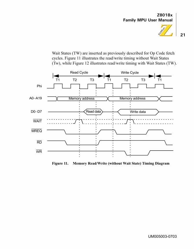
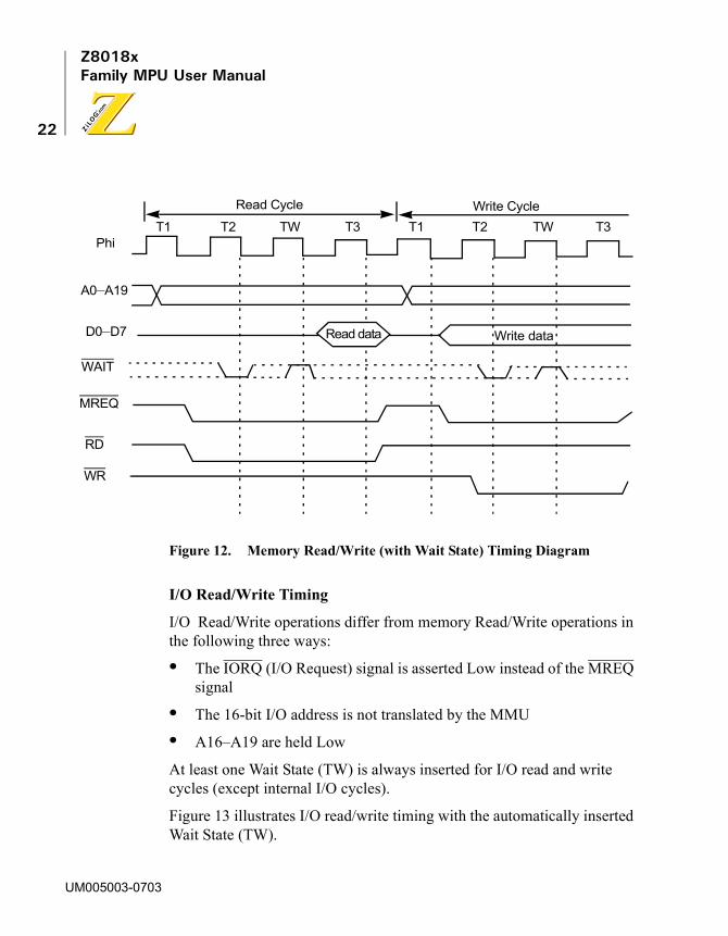
Wait States (TW) are inserted as previously described for Op Code fetch cycles. Figure 11 illustrates the read/write timing without Wait States (Tw), while Figure 12 illustrates read/write timing with Wait States (TW).
Figure 11. Memory Read/Write (without Wait State) Timing Diagram
T1 T1T2 T3 T1 T2 T3
Phi
A0–A19
D0–D7
WR
MREQ
RD
WAIT
Read Cycle Write Cycle
Memory addressMemory address
Write dataRead data
UM005003-0703
Z8018xFamily MPU User Manual
22
Figure 12. Memory Read/Write (with Wait State) Timing Diagram
I/O Read/Write Timing
I/O Read/Write operations differ from memory Read/Write operations in the following three ways:
• The IORQ (I/O Request) signal is asserted Low instead of the MREQ signal
• The 16-bit I/O address is not translated by the MMU
• A16–A19 are held Low
At least one Wait State (TW) is always inserted for I/O read and write cycles (except internal I/O cycles).
Figure 13 illustrates I/O read/write timing with the automatically inserted Wait State (TW).
T1 T1T2 TW T3 T2 T3Phi
A0–A19
D0–D7
WR
MREQ
RD
WAIT
Read Cycle Write CycleTW
Read data Write data
UM005003-0703

Z8018xFamily MPU User Manual
23
Figure 13. I/O Read/Write Timing Diagram
Basic Instruction Timing
An instruction may consist of a number of machine cycles including Op Code fetch, operand fetch, and data read/write cycles. An instruction may also include cycles for internal processes which make the bus IDLE. The example in Figure 14 illustrates the bus timing for the data transfer instruction LD (IX+d),g.
T1 T1T2 TW T3 T2 T3Phi
A0–A19
D0–D7
WR
IORQ
RD
WAIT
I/O Read Cycle I/O Write Cycle
Write data
TW
I/O address I/O address
Read data
UM005003-0703

Z8018xFamily MPU User Manual
24
Figure 14. Instruction Timing Diagram
This instruction moves the contents of a CPU register (g) to the memory location with address computed by adding a signed 8-bit displacement (d) to the contents of an index register (IX).
The instruction cycle begins with the two machine cycles to read the two byte instruction Op Code as indicated by M1 Low. Next, the instruction operand (d) is fetched.
MemoryWrite Cycle
Next instructionFetch Cycle
CPU internalOperation
Displacement Read Cycle
2nd Op Code Fetch Cycle
1st Op Code Fetch Cycle
T1 T2 T3 T1 T3 T1T2 T2 T3 T1 T1 T1 T1 T1T2 T3 T2
PC+3IX+dPC+2PC+1PC
g(7OH–77H)(DDH) d
MC1 MC2 MC3 MC4 MC5 MC6 MC7
NOTE: d = displacementg = register contents
Machine Cycle
WR
RD
MREQ
Phi
A0–A19
D0–D7
M1
UM005003-0703

Z8018xFamily MPU User Manual
25
The external bus is IDLE while the CPU computes the effective address. Finally, the computed memory location is written with the contents of the CPU register (g).
RESET Timing
Figure 15 depicts the Z8X180 hardware RESET timing. If the RESET pin is Low for six or more clock cycles, processing is terminated and the Z8X180 restarts execution from (logical and physical) address 00000H.
Figure 15. RESET Timing Diagram
BUSREQ/BUSACK Bus Exchange Timing
The Z8X180 can coordinate the exchange of control, address and data bus ownership with another bus master. The alternate bus master can request the bus release by asserting the BUSREQ (Bus Request) input Low. After the Z8X180 releases the bus, it relinquishes control to the alternate bus master by asserting the BUSACK (Bus Acknowledge) output Low.
The bus may be released by the Z8X180 at the end of each machine cycle. In this context, a machine cycle consists of a minimum of three clock cycles (more if wait states are inserted) for Op Code fetch, memory read/write, and I/O read/write cycles. Except for these cases, a machine cycle corresponds to one clock cycle.
Phi
A0–A19
RESET
RESET
High impedance Restart address (00000H)
RESET StartOp Code Fetch Cycle
T1 T2
6 or more clocks
UM005003-0703

Z8018xFamily MPU User Manual
26
When the bus is released, the address (A0–A19), data (D0–D7), and control (MREQ, IORQ, RD, and WR) signals are placed in the high impedance state.
Dynamic RAM refresh is not performed when the Z8X180 has released the bus. The alternate bus master must provide dynamic memory refreshing if the bus is released for long periods of time.
Figure 16 illustrates BUSREQ/BUSACK bus exchange during a memory read cycle. Figure 17 illustrates bus exchange when the bus release is requested during a Z8X180 CPU internal operation. BUSREQ is sampled at the falling edge of the system clock prior to T3, T1 and Tx (BUS RELEASE state). If BUSREQ is asserted Low at the falling edge of the clock state prior to Tx, another Tx is executed.
Figure 16. Bus Exchange Timing During Memory Read
Phi
A0–A19
T1 T1TXTXT3TWT2 T1
RD, WR
D0–D7
MREQIORQ
BUSREQ
BUSACK
CPU memory read cycle Bus release cycle CPU cycle
UM005003-0703

Z8018xFamily MPU User Manual
27
Figure 17. Bus Exchange Timing During CPU Internal Operation
Wait State Generator
To ease interfacing with slow memory and I/O devices, the Z8X180 uses Wait States (TW) to extend bus cycle timing. A Wait State(s) is inserted based on the combined (logical OR) state of the external WAIT input and an internal programmable wait state (TW) generator. Wait States (TW) can be inserted in both CPU execution and DMA transfer cycles.
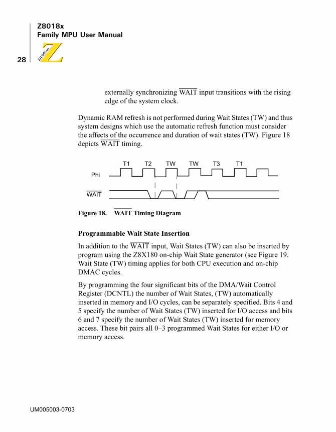
When the external WAIT input is asserted Low, Wait State(s) (TW) are inserted between T2 and T3 to extend the bus cycle duration. The WAIT input is sampled at the falling edge of the system clock in T2 or TW. If the WAIT input is asserted Low at the falling edge of the system clock in TW, another TW is inserted into the bus cycle.
WAIT input transitions must meet specified setup and hold times. This specification can easily be accomplished by
Phi
A0–A19
RD, WR
D0–D7MREQIORQ
BUSREQ
BUSACK
CPU Internal Operation Bus Release Cycle CPU Cycle
T1 T1 T1 TX T1TXT1 TX
Note:
UM005003-0703
Z8018xFamily MPU User Manual
28
externally synchronizing WAIT input transitions with the rising edge of the system clock.
Dynamic RAM refresh is not performed during Wait States (TW) and thus system designs which use the automatic refresh function must consider the affects of the occurrence and duration of wait states (TW). Figure 18 depicts WAIT timing.
Figure 18. WAIT Timing Diagram
Programmable Wait State Insertion
In addition to the WAIT input, Wait States (TW) can also be inserted by program using the Z8X180 on-chip Wait State generator (see Figure 19. Wait State (TW) timing applies for both CPU execution and on-chip DMAC cycles.
By programming the four significant bits of the DMA/Wait Control Register (DCNTL) the number of Wait States, (TW) automatically inserted in memory and I/O cycles, can be separately specified. Bits 4 and 5 specify the number of Wait States (TW) inserted for I/O access and bits 6 and 7 specify the number of Wait States (TW) inserted for memory access. These bit pairs all 0–3 programmed Wait States for either I/O or memory access.
T1
Phi
WAIT
T2 TW TW T3 T1
UM005003-0703

Z8018xFamily MPU User Manual
29
Figure 19. Memory and I/O Wait State Insertion (DCNTL – DMA/Wait Control Register)
The number of Wait States (TW) inserted in a specific cycle is the maximum of the number requested by the WAIT input, and the number automatically generated by the on-chip Wait State generator.
Bit 7, 6: MWI1 MWI0, (Memory Wait Insertion)
For CPU and DMAC cycles which access memory (including memory mapped I/O), zero to three Wait States may be automatically inserted depending on the programmed value in MWI1 and MWI0 as depicted in Table 3
Bit 5, 4: IWI1, IWI0 (I/O Wait Insertion)
For CPU and DMA cycles which access external I/O (and interrupt acknowledge cycles), one to six Wait States (TW) may be automatically
Table 3. Memory Wait States
MW11 MWI0 The Number of Wait States
0 0 0
0 1 1
1 0 2
1 1 3
Bit 7 6 5 4
MWI1 MWI0 MWI1 MWI0
R/W R/W R/W R/W
UM005003-0703

Z8018xFamily MPU User Manual
30
inserted depending on the programmed value in IWI1 and IWI0. Refer to Table 4.
WAIT Input and RESET
During RESET, MWI1, MWI0 IWI1 and IWI0, are all 1, selecting the maximum number of Wait States (TW) (three for memory accesses, four for external I/O accesses).
Table 4. Wait State Insertion
IWI1 IWI0
The Number of Wait States
For external I/O registers accesses
For internal I/0registers accesses
For INT0 interrupt acknowledge cycles when M1 is Low
For INT1, INT2 and internal interrupts acknowledge cycles(Note 2)
For NMI interruptacknowledge cycleswhen M1 is Low(Note 2)
0 0 1 0(Note 1)
2 2 0
0 1 2 4
1 0 3 5
1 1 4 6
Note:
1. For Z8X180 internal I/O register access (I/O addresses 0000H-003FH), IWI1 and IWI0 do not determine wait state (TW) timing. For ASCI, CSI/O and PRT Data Register accesses, 0 to 4 Wait States (TW) are generated. The number of Wait States inserted during access to these registers is a function of internal synchronization requirements and CPU state. All other on-chip I/O register accesses (that is, MMU, DMAC, ASCI Control Registers, for instance.) have no Wait States inserted and thus require only three clock cycles.
2. For interrupt acknowledge cycles in which M1 is High, such as interrupt vector table read and PC stacking cycle, memory access timing applies.
UM005003-0703
Z8018xFamily MPU User Manual
31
Also, the WAIT input is ignored during RESET. For example, if RESET is detected while the Z8X180 is in a Wait State (TW), the Wait Stated cycle in progress is aborted, and the RESET sequence initiated. Thus, RESET has higher priority than WAIT.
HALT and Low Power Operation Modes (Z80180-Class Processors Only)
The Z80180 can operate in two different modes:
• HALT mode
• IOSTOP mode
and two low-power operation modes:
• SLEEP
• SYSTEM STOP
In all operating modes, the basic CPU clock (XTAL, EXTAL) must remain active.
HALT Mode
HALT mode is entered by execution of the HALT instruction (Op Code 76H) and has the following characteristics:
• The internal CPU clock remains active
• All internal and external interrupts can be received
• Bus exchange (BUSREQ and BUSACK) can occur
• Dynamic RAM refresh cycle (RFSH) insertion continues at the programmed interval
• I/O operations (ASCI, CSI/O and PRT) continue
• The DMAC can operate
UM005003-0703
Z8018xFamily MPU User Manual
32
• The HALT output pin is asserted Low
• The external bus activity consists of repeated dummy fetches of the Op Code following the HALT instruction.
Essentially, the Z80180 operates normally in HALT mode, except that instruction execution is stopped.
HALT mode can be exited in the following two ways:
• RESET Exit from HALT ModeIf the RESET input is asserted Low for at least six clock cycles, HALT mode is exited and the normal RESET sequence (restart at address 00000H) is initiated.
• Interrupt Exit from HALT modeWhen an internal or external interrupt is generated, HALT mode is exited and the normal interrupt response sequence is initiated.
If the interrupt source is masked (individually by enable bit, or globally by IEF1 state), the Z80180 remains in HALT mode. However, NMI interrupt initiates the normal NMI interrupt response sequence independent of the state of IEF1.
HALT timing is illustrated in Figure 20.
UM005003-0703

Z8018xFamily MPU User Manual
33
.
Figure 20. HALT Timing Diagram
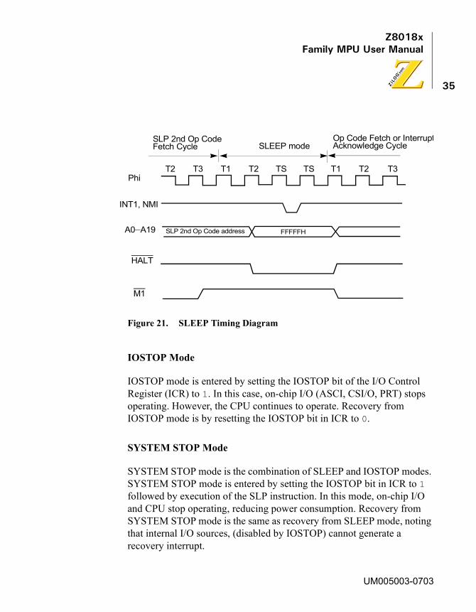
SLEEP Mode
SLEEP mode is entered by execution of the 2-byte SLP instruction. SLEEP mode contains the following characteristics:
• The internal CPU clock stops, reducing power consumption
• The internal crystal oscillator does not stop
• Internal and external interrupt inputs can be received
• DRAM refresh cycles stop
• I/O operations using on-chip peripherals continue
• The internal DMAC stop
• BUSREQ can be received and acknowledged
• Address outputs go High and all other control signal outputs become inactive High
T1
M1
RD
MREQ
Phi
A0–A19
INT1, NMI
T3 T1 T2 T3 T1 T2
HALT Op Code HALT modeInterrupt acknowledge cycle
HALT
HALT Op Code address HALT Op Code address + 1
Fetch Cycle
UM005003-0703

Z8018xFamily MPU User Manual
34
• Data Bus, 3-state
SLEEP mode is exited in one of two ways as described below.
• RESET Exit from SLEEP mode. If the RESET input is held Low for at least six clock cycles, it exits SLEEP mode and begins the normal RESET sequence with execution starting at address (logical and physical) 00000H.
• Interrupt Exit from SLEEP mode. The SLEEP mode is exited by detection of an external (NMI, INT0, INT2) or internal (ASCI,CSI/O, PRT) interrupt.
In case of NMI, SLEEP mode is exited and the CPU begins the normal NMI interrupt response sequence.
In the case of all other interrupts, the interrupt response depends on the state of the global interrupt enable flag IEF1 and the individual interrupt source enable bit.
If the individual interrupt condition is disabled by the corresponding enable bit, occurrence of that interrupt is ignored and the CPU remains in the SLEEP mode.
Assuming the individual interrupt condition is enabled, the response to that interrupt depends on the global interrupt enable flag (IEF1). If interrupts are globally enabled (IEF1 is 1) and an individually enabled interrupt occurs, SLEEP mode is exited and the appropriate normal interrupt response sequence is executed.
If interrupts are globally disabled (IEF1 is 0) and an individually enabled interrupt occurs, SLEEP mode is exited and instruction execution begins with the instruction following the SLP instruction. This feature provides a technique for synchronization with high speed external events without incurring the latency imposed by an interrupt response sequence.
Figure 21 depicts SLEEP timing.
UM005003-0703
Z8018xFamily MPU User Manual
35
Figure 21. SLEEP Timing Diagram
IOSTOP Mode
IOSTOP mode is entered by setting the IOSTOP bit of the I/O Control Register (ICR) to 1. In this case, on-chip I/O (ASCI, CSI/O, PRT) stops operating. However, the CPU continues to operate. Recovery from IOSTOP mode is by resetting the IOSTOP bit in ICR to 0.
SYSTEM STOP Mode
SYSTEM STOP mode is the combination of SLEEP and IOSTOP modes. SYSTEM STOP mode is entered by setting the IOSTOP bit in ICR to 1 followed by execution of the SLP instruction. In this mode, on-chip I/O and CPU stop operating, reducing power consumption. Recovery from SYSTEM STOP mode is the same as recovery from SLEEP mode, noting that internal I/O sources, (disabled by IOSTOP) cannot generate a recovery interrupt.
T2
M1
Phi
A0–A19
HALT
T1 T2 TS TS T1 T2 T3
INT1, NMI
SLP 2nd Op Code SLEEP mode
Op Code Fetch or InterruptAcknowledge CycleFetch Cycle
SLP 2nd Op Code address FFFFFH
T3
UM005003-0703
Z8018xFamily MPU User Manual
36
Low Power Modes (Z8S180/Z8L180 only)The following section is a detailed description of the enhancements to the Z8S180/L180 from the standard Z80180 in the areas of STANDBY, IDLE and STANDBY QUICK RECOVERY modes.
Add-On FeaturesThere are five different power-down modes. SLEEP and SYSTEM STOP are inherited from the Z80180. In SLEEP mode, the CPU is in a stopped state while the on-chip I/Os are still operating. In I/O STOP mode, the on-chip I/Os are in a stopped state while leaving the CPU running. In SYSTEM STOP mode, both the CPU and the on-chip I/Os are in the stopped state to reduce current consumption. The Z8S180 features two additional power-down modes, STANDBY and IDLE, to reduce current consumption even further. The differences in these power-down modes are summarized in Table 5.
UM005003-0703

Z8018xFamily MPU User Manual
37
STANDBY ModeThe Z8S180/Z8L180 is designed to save power. Two low-power programmable power-down modes have been added:
• STANDBY mode
• IDLE mode
The STANDBY/IDLE mode is selected by multiplexing bits 1 and 3 of the CPU Control Register (CCR, I/O Address = 1FH).
To enter STANDBY mode:
Table 5. Power-Down Modes (Z8S180/Z8L180-Class Processors Only)
Power-Down Modes CPU Core
On-ChipI/O Osc. CLKOUT
Recovery Source
Recovery Time (Minimum)
SLEEP Stop Running Running Running RESET, Interrupts
1.5 Clock
I/O STOP Running Stop Running Running By Programming
–
SYSTEM STOP
Stop Stop Running Running RESET, Interrupts
1.5 Clock
IDLE † Stop Stop Running Stop RESET, Interrupts, BUSREQ
8 + 1.5 Clock
STANDBY † Stop Stop Stop Stop RESET, Interrupts, BUSREQ
217 + 1.5 Clock (Normal Recovery)26 + 1.5 Clock (Quick Recovery)
† IDLE and STANDBY modes are only offered in the Z8S180. The minimum recovery time can be achieved if INTERRUPT is used as the Recovery Source.
UM005003-0703
Z8018xFamily MPU User Manual
38
1. Set bits 6 and 3 to 1 and 0, respectively.
2. Set the I/O STOP bits (bit 5 of ICR, I/O Address = 3FH) to 1.
3. Execute the SLEEP instruction.
When the device is in STANDBY mode, it performs similar to the SYSTEM STOP mode as it exists on the Z80180-class processors, except that the STANDBY mode stops the external oscillator, internal clocks and reduces power consumption to 50 �A (typical).
Because the clock oscillator has been stopped, a restart of the oscillator requires a period of time for stabilization. An 18-bit counter has been added in the Z8S180Z8L180 to allow for oscillator stabilization. When the part receives an external IRQ or BUSREQ during STANDBY mode, the oscillator is restarted and the timer counts down 217 counts before acknowledgment is sent to the interrupt source.
The recovery source must remain asserted for the duration of the 217 count, otherwise STANDBY restarts.
STANDBY Mode Exit with BUS REQUESTOptionally, if the BREXT bit (D5 of CPU Control Register) is set to 1, the Z8S180 exits STANDBY mode when the BUSREQ input is asserted. The crystal oscillator is then restarted. An internal counter automatically provides time for the oscillator to stabilize, before the internal clocking and the system clock output of the Z8S180 are resumed.
The Z8S180 relinquishes the system bus after the clocking is resumed by:
• 3-State the address outputs A19–A0
• 3-State the bus control outputs MREQ, IORQ, RD, and WR
• Asserting BUSACK
The Z8S180 regains the system bus when BUSREQ is deactivated. The address outputs and the bus control outputs are then driven High. The STANDBY mode is exited.
UM005003-0703

Z8018xFamily MPU User Manual
39
If the BREXT bit of the CPU Control Register (CCR) is cleared, asserting the BUSREQ does not cause the Z8S180/Z8L180-class processors to exit STANDBY mode.
If STANDBY mode is exited because of a reset or an external interrupt, the Z8S180/Z8L180-class processors remains relinquished from the system bus as long as BUSREQ is active.
STANDBY Mode EXit with External InterruptsSTANDBY mode can be exited by asserting input NMI. The STANDBY mode may also exit by asserting INT0. INT1 or INT2, depending on the conditions specified in the following paragraphs.
INT0 wake-up requires assertion throughout duration of clock stabilization time (217 clocks).
If exit conditions are met, the internal counter provides time for the crystal oscillator to stabilize, before the internal clocking and the system clock output within the Z8S180/Z8L180-class processors resume.
• Exit with Non-Maskable Interrupts
If NMI is asserted, the CPU begins a normal NMI interrupt acknowledge sequence after clocking resumes.
• Exit with External Maskable Interrupts
If an External Maskable Interrupt input is asserted, the CPU responds according to the status of the Global Interrupt Enable Flag IEF1 (determined by the ITE1 bit) and the settings of the corresponding interrupt enable bit in the Interrupt/Trap Control Register (ITC: I/O Address = 34H).
If an interrupt source is disabled in the ITC, asserting the corresponding interrupt input does not cause the Z8S180/Z8L180-class processors to exit STANDBY mode. This condition is true regardless of the state of the Global Interrupt Enable Flag IEF1.
UM005003-0703

Z8018xFamily MPU User Manual
40
If the Global Interrupt Enable Flag IEF1 is set to 1, and if an interrupt source is enabled in the ITC, asserting the corresponding interrupt input causes the Z8S180/Z8L180-class processors to exit STANDBY mode. The CPU performs an interrupt acknowledge sequence appropriate to the input being asserted when clocking is resumed if:
• The interrupt input follows the normal interrupt daisy-chain protocol
• The interrupt source is active until the acknowledge cycle is complete
If the Global Interrupt Enable Flag IEF1 is disabled (reset to 0) and if an interrupt source is enabled in the ITC, asserting the corresponding interrupt input still causes the Z8S180/Z8L180-class processors to exit STANDBY mode. The CPU proceeds to fetch and execute instructions that follow the SLEEP instruction when clocking resumes.
If the Extend Maskable Interrupt input is not active until clocking resumes, the Z8S180/Z8L180-class processors do not exit STANDBY mode. If the Non-Maskable Interrupt (NMI) is not active until clocking resumes, the Z8S180/Z8L180-class processors still exits the STANDBY mode even if the interrupt sources go away before the timer times out, because NMI is edge-triggered. The condition is latched internally when NMI is asserted Low.
IDLE ModeIDLE mode is another power-down mode offered by the Z8S180/Z8L180-class processors.
1. Set bits 6 and 3 to 0 and 1, respectively.
2. Set the I/O STOP bit (bit 5 of ICR, I/O Address = 3FH to 1.
3. Execute the SLEEP instruction
When the part is in IDLE mode, the clock oscillator is kept oscillating, but the clock to the rest of the internal circuit, including the CLKOUT, is stopped completely. IDLE mode is exited in a similar way as STANDBY mode, using RESET, BUS REQUEST or EXTERNAL INTERRUPTS,
UM005003-0703

Z8018xFamily MPU User Manual
41
except that the 217 bit wake-up timer is bypassed. All control signals are asserted eight clock cycles after the exit conditions are gathered.
STANDBY-QUICK RECOVERY Mode
STANDBY-QUICK RECOVERY mode is an option offered in STANDBY mode to reduce the clock recovery time in STANDBY mode from 217 clock cycles (4 �s at 33 MHz) to 26 clock cycles (1.9 �s at 33 MHz). This feature can only be used when providing an oscillator as clock source.
To enter STANDBY-QUICK RECOVERY mode:
1. Set bits 6 and 3 to 1 and 1, respectively.
2. Set the I/O STOP bit (bit 5 of ICR, I/O Address = 3FH) to 1.
3. Execute the SLEEP instruction
When the part is in STANDBY-QUICK RECOVERY mode, the operation is identical to STANDBY mode except when exit conditions are gathered, using RESET, BUS REQUEST or EXTERNAL INTERRUPTS. The clock and other control signals are recovered sooner than the STANDBY mode.
If STANDBY-QUICK RECOVERY is enabled, the user must ensure stable oscillation is obtained within 64 clock cycles
Internal I/O Registers
The Z8X180 internal I/O Registers occupy 64 I/O addresses (including reserved addresses). These registers access the internal I/O modules (ASCI, CSI/O, PRT) and control functions (DMAC, DRAM refresh, interrupts, wait state generator, MMU and I/O relocation).
Note:
UM005003-0703
Z8018xFamily MPU User Manual
42
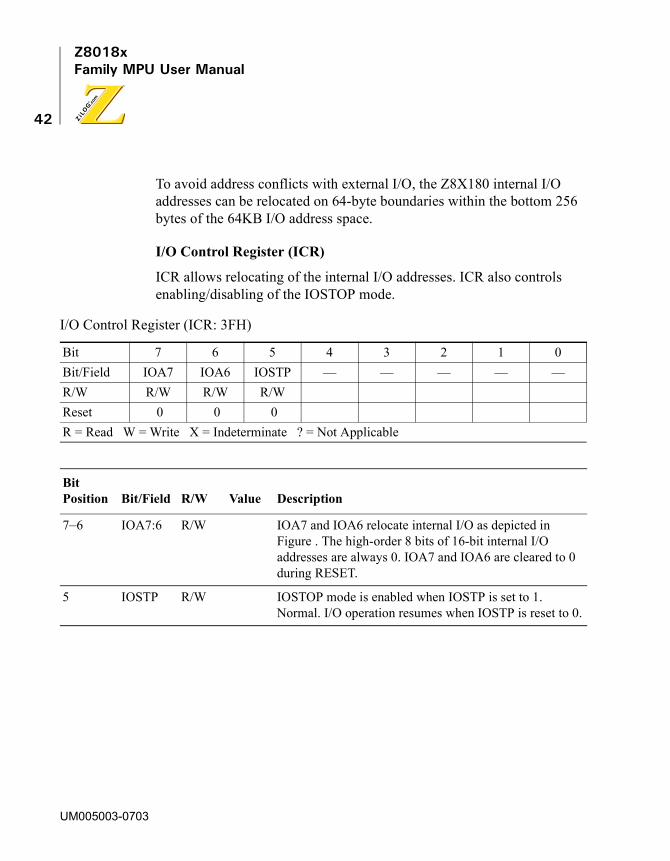
To avoid address conflicts with external I/O, the Z8X180 internal I/O addresses can be relocated on 64-byte boundaries within the bottom 256 bytes of the 64KB I/O address space.
I/O Control Register (ICR)
ICR allows relocating of the internal I/O addresses. ICR also controls enabling/disabling of the IOSTOP mode.
I/O Control Register (ICR: 3FH)
Bit 7 6 5 4 3 2 1 0Bit/Field IOA7 IOA6 IOSTP — — — — —R/W R/W R/W R/W Reset 0 0 0 R = Read W = Write X = Indeterminate ? = Not Applicable
BitPosition Bit/Field R/W Value Description
7–6 IOA7:6 R/W IOA7 and IOA6 relocate internal I/O as depicted in Figure . The high-order 8 bits of 16-bit internal I/O addresses are always 0. IOA7 and IOA6 are cleared to 0 during RESET.
5 IOSTP R/W IOSTOP mode is enabled when IOSTP is set to 1. Normal. I/O operation resumes when IOSTP is reset to 0.
UM005003-0703

Z8018xFamily MPU User Manual
43
Figure 22. I/O Address Relocation
Internal I/O Registers Address Map
The internal I/O register addresses are described in Table 6 and Table 7. These addresses are relative to the 64-byte boundary base address specified in ICR.
I/O Addressing Notes
The internal I/O register addresses are located in the I/O address space from 0000H to 00FFH (16-bit I/O addresses). Thus, to access the internal I/O registers (using I/O instructions), the high-order 8 bits of the 16-bitI/O address must be 0.
The conventional I/O instructions (OUT (m), A/IN A, (m) / OUTI/INI, for example) place the contents of a CPU register on the high-order 8 bits of the address bus, and thus may be difficult to use for accessing internal I/O registers.
For efficient internal I/O register access, a number of new instructions have been added, which force the high-order 8 bits of the 16-bit I/O
IOA7 — IOA6 = 1 1
IOA7 — IOA6 = 1 0
IOA7 — IOA6 = 0 1
IOA7 — IOA6 = 0 0
00FFH
00C0H
0080H007FH
0040H003FH
0000H
00BFH
UM005003-0703

Z8018xFamily MPU User Manual
44
address to 0. These instructions are IN0, OUT0, OTIM, OTIMR, OTDM, OTDMR and TSTIO (see Instruction Set).
When writing to an internal I/O register, the same I/O write occurs on the external bus. However, the duplicate external I/O write cycle exhibits internal I/O write cycle timing. For example, the WAIT input and programmable Wait State generator are ignored. Similarly, internal I/O read cycles also cause a duplicate external I/O read cycle. However, the external read data is ignored by the Z8X180.
Normally, external I/O addresses should be chosen to avoid overlap with internal I/O addresses and duplicate I/O accesses.
Table 6. I/O Address Map for Z80180-Class Processors Only
Register Mnemonic
Address
Binary Hex Page
ASCI ASCI Control Register A Ch 0 CNTLA0 XX000000 00H 125
ASCI Control Register A Ch 1 CNTLA1 XX000001 01H 128
ASCI Control Register B Ch 0 CNTLB0 XX000010 02H 132
ASCI Control Register B Ch 1 CNTLB1 XX000011 03H 132
ASCI Status Register Ch 0 STAT0 XX000100 04H 120
ASCI Status Register Ch 1 STAT1 XX000101 05H 123
ASCI Transmit Data Register Ch 0 TDR0 XX000110 06H 118
ASCI Transmit Data Register Ch 1 TDR1 XX000111 07H 118
ASCI Receive Data Register Ch 0 RDR0 XX001000 08H 119
ASCI Receive Data Register Ch 1 RDR1 XX001001 09H 119
CSI/O CSI/O Control Register CNTR XX001010 0AH 147
CSI/O Transmit/Receive Data Register TRD XX1011 0BH 149
UM005003-0703

Z8018xFamily MPU User Manual
45
Timer Data Register Ch 0 L TMDR0L XX001100 0CH 159
Data Register Ch 0 H TMDR0H XX001101 0DH 159
Reload Register Ch 0 L RLDR0L XX001110 0EH 159
Reload Register Ch 0 H RLDR0H XX001111 0FH 159
Timer Control Register TCR XX010000 10H 161
Reserved XX010001 11H
XX010011 13H
Data Register Ch 1 L TMDR1L XX010100 14H 160
Data Register Ch 1 H TMDR1H XX010101 15H 160
Reload Register Ch 1 L RLDR1L XX010110 16H 159
Reload Register Ch 1 H RLDR1H XX010111 17H 159
Others Free Running CounterReserved
FRC XX011000 18H 172
XX011001 19H
XX011111 1FH
Table 6. I/O Address Map for Z80180-Class Processors Only (Continued)
Register Mnemonic
Address
Binary Hex Page
UM005003-0703

Z8018xFamily MPU User Manual
46
DMA DMA Source Address Register Ch 0L SAR0L XX100000 20H 93
DMA Source Address Register Ch 0H SAR0H XX100001 21H 93
DMA Source Address Register Ch 0B SAR0B XX100010 22H 93
DMA Destination Address Register Ch 0L
DAR0L XX100011 23H 94
DMA Destination Address Register Ch 0H
DAR0H XX100100 24H 94
DMA Destination Address Register Ch 0B
DAR0B XX100101 25H 94
DMA Byte Count Register Ch 0L BCR0L XX100110 26H 94
DMA Byte Count Register Ch 0H BCR0H XX100111 27H 94
DMA Memory Address Register Ch 1L MAR1L XX101000 28H 94
DMA Memory Address Register Ch 1H MAR1H XX101001 29H 94
DMA Memory Address Register Ch 1B MAR1B XX101010 2AH 94
DMA I/0 Address Register Ch 1L IAR1L XX101011 2BH 102
DMA I/0 Address Register Ch 1H IAR1H XX101100 2CH 102
Reserved XX101101 2DH
DMA Byte Count Register Ch 1L BCR1L XX101110 2EH 94
DMA Byte Count Register Ch 1H BCR1H XX101111 2FH 94
DMA Status Register DSTAT XX110000 30H 95
DMA Mode Register DMODE XX110001 31H 97
DMA/WAIT Control Register DCNTL XX110010 32H 101
Table 6. I/O Address Map for Z80180-Class Processors Only (Continued)
Register Mnemonic
Address
Binary Hex Page
UM005003-0703
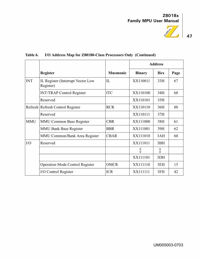
Z8018xFamily MPU User Manual
47
INT IL Register (Interrupt Vector Low Register)
IL XX110011 33H 67
INT/TRAP Control Register ITC XX110100 34H 68
Reserved XX110101 35H
Refresh Refresh Control Register RCR XX110110 36H 88
Reserved XX110111 37H
MMU MMU Common Base Register CBR XX111000 38H 61
MMU Bank Base Register BBR XX111001 39H 62
MMU Common/Bank Area Register CBAR XX111010 3AH 60
I/O Reserved XX111011 3BH
XX111101 3DH
Operation Mode Control Register OMCR XX111110 3EH 15
I/O Control Register ICR XX111111 3FH 42
Table 6. I/O Address Map for Z80180-Class Processors Only (Continued)
Register Mnemonic
Address
Binary Hex Page
UM005003-0703

Z8018xFamily MPU User Manual
48
Table 7. I/O Address Map (Z8S180/Z8L180-Class Processors Only)
Register Mnemonic
Address
Binary Hex Page
ASCI ASCI Control Register A Ch 0 CNTLA0 XX000000 00H 125
ASCI Control Register A Ch 1 CNTLA1 XX000001 01H 128
ASCI Control Register B Ch 0 CNTLB0 XX000010 02H 132
ASCI Control Register B Ch 1 CNTLB1 XX000011 03H 132
ASCI Status Register Ch 0 STAT0 XX000100 04H 120
ASCI Status Register Ch 1 STAT1 XX000101 05H 123
ASCI Transmit Data Register Ch 0 TDR0 XX000110 06H 118
ASCI Transmit Data Register Ch 1 TDR1 XX000111 07H 118
ASCI Receive Data Register Ch 0 RDR0 XX001000 08H 119
ASCI Receive Data Register Ch 1 RDR1 XX001001 09H 119
ASCI0 Extension Control Register 0 ASEXT0 XX010010 12H 135
ASCI1 Extension Control Register 1 ASEXT1 XX010011 13H 136
ASCI0 Time Constant Low ASTC0L XX011010 1AH 137
ASCI0 Time Constant High ASTC0H XX001011 1BH 137
ASCI1 Time Constant Low ASCT1L XX001100 1CH 138
ASCI1 Time Constant High ASCT1H XX001101 1DH 138
CSI0 CSI0 Control Register CNTR XX001010 0AH 147
CSI0 Transmit/Receive Data Register TRD XX1011 0BH 149
UM005003-0703

Z8018xFamily MPU User Manual
49
Timer Data Register Ch 0 L TMDR0L XX001100 0CH 159
Data Register Ch 0 H TMDR0H XX001101 0DH 159
Reload Register Ch 0 L RLDR0L XX001110 0EH 159
Reload Register Ch 0 H RLDR0H XX001111 0FH 159
Timer Control Register TCR XX010000 10H 161
Reserved XX010001 11H
Data Register Ch 1 L TMDR1L XX010100 14H 160
Data Register Ch 1 H TMDR1H XX010101 15H 160
Reload Register Ch 1 L RLDR1L XX010110 16H 160
Reload Register Ch 1 H RLDR1H XX010111 17H 160
Others Free Running CounterReserved
FRC XX011000 18H 172
XX011001 19H
XX011111 1DH
Clock Multiplier Register CMR XX011110 1EH 52
CPU Control Register CCR XX011111 1FH 53
Table 7. I/O Address Map (Z8S180/Z8L180-Class Processors Only) (Continued)
Register Mnemonic
Address
Binary Hex Page
UM005003-0703
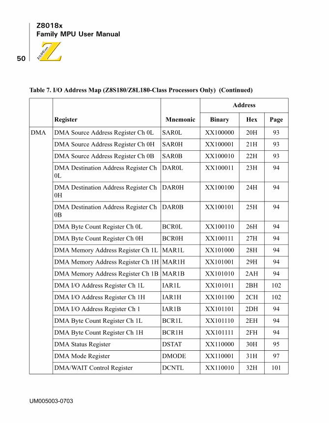
Z8018xFamily MPU User Manual
50
DMA DMA Source Address Register Ch 0L SAR0L XX100000 20H 93
DMA Source Address Register Ch 0H SAR0H XX100001 21H 93
DMA Source Address Register Ch 0B SAR0B XX100010 22H 93
DMA Destination Address Register Ch 0L
DAR0L XX100011 23H 94
DMA Destination Address Register Ch 0H
DAR0H XX100100 24H 94
DMA Destination Address Register Ch 0B
DAR0B XX100101 25H 94
DMA Byte Count Register Ch 0L BCR0L XX100110 26H 94
DMA Byte Count Register Ch 0H BCR0H XX100111 27H 94
DMA Memory Address Register Ch 1L MAR1L XX101000 28H 94
DMA Memory Address Register Ch 1H MAR1H XX101001 29H 94
DMA Memory Address Register Ch 1B MAR1B XX101010 2AH 94
DMA I/O Address Register Ch 1L IAR1L XX101011 2BH 102
DMA I/O Address Register Ch 1H IAR1H XX101100 2CH 102
DMA I/O Address Register Ch 1 IAR1B XX101101 2DH 94
DMA Byte Count Register Ch 1L BCR1L XX101110 2EH 94
DMA Byte Count Register Ch 1H BCR1H XX101111 2FH 94
DMA Status Register DSTAT XX110000 30H 95
DMA Mode Register DMODE XX110001 31H 97
DMA/WAIT Control Register DCNTL XX110010 32H 101
Table 7. I/O Address Map (Z8S180/Z8L180-Class Processors Only) (Continued)
Register Mnemonic
Address
Binary Hex Page
UM005003-0703

Z8018xFamily MPU User Manual
51
INT IL Register (Interrupt Vector Low Register)
IL XX110011 33H 67
INT/TRAP Control Register ITC XX110100 34H 68
Reserved XX110101 35H
Refresh Refresh Control Register RCR XX110110 36H 88
Reserved XX110111 37H
MMU MMU Common Base Register CBR XX111000 38H 61
MMU Bank Base Register BBR XX111001 39H 62
MMU Common/Bank Area Register CBAR XX111010 3AH 60
I/O Reserved XX111011 3BH
XX111101 3DH
Operation Mode Control Register OMCR XX111110 3EH 15
I/O Control Register ICR XX111111 3FH 42
Table 7. I/O Address Map (Z8S180/Z8L180-Class Processors Only) (Continued)
Register Mnemonic
Address
Binary Hex Page
UM005003-0703

Z8018xFamily MPU User Manual
52
Clock Multiplier Register (CMR: 1EH) (Z8S180/L180-Class Processors Only)
Bit 7 6 0Bit/Field X2 ReservedR/W R/W ?Reset 0 1Note: R = Read W = Write X = Indeterminate ? = Not Applicable
BitPosition Bit/Field R/W Value Description
7 X2 Clock Multiplier Mode
R/W01
X2 Clock Multiplier ModeDisableEnable
6–0 Reserved ? ? Reserved
UM005003-0703

Z8018xFamily MPU User Manual
53
CPU Control Register (CCR: 1FH) (Z8S180/L180-Class Processors Only)
Bit 7 6 5 4 3 2 1 0Bit/Field Clock
DivideSTAND
BY/IDLE Enable
BREXT LNPHI STANDBY/
IDLE Enable
LNIO LNCPUCTL
LNAD/DATA
R/W R/W R/W R/W R/W R/W R/W R/W R/WReset 0 0 0 0 0 0 0 0Note: R = Read W = Write X = Indeterminate ? = Not Applicable
BitPosition Bit/Field R/W Value Description
7 Clock Divide
R/W 01
XTAL/2XTAL/1
6 STANDBY/IDLE Mode
R/W00011011
In conjunction with Bit 3No STANDBYIDLE after SLEEPSTANDBY after SLEEPSTANDBY after SLEEP 64 Cycle Exit (Quick Recovery)
5 BREXT R/W 01
Ignore BUSREQ in STANDBY/IDLESTANDBY/IDLE exit on BUSREQ
4 LNPHI R/W 01
Standard Drive33% Drive on EXTPHI Clock
3 STANDBY/IDLE Mode
R/W00011011
In conjunction with Bit 6No STANDBYIDLE after SLEEPSTANDBY after SLEEPSTANDBY after SLEEP 64 Cycle Exit (Quick Recovery)
UM005003-0703

Z8018xFamily MPU User Manual
54
Memory Management Unit (MMU)
The Z8X180 features an on-chip MMU which performs the translation of the CPU 64KB (16-bit addresses 0000H to FFFFH) logical memory address space into a 1024KB (20-bit addresses 00000H to FFFFFH) physical memory address space. Address translation occurs internally in parallel with other CPU operation.
Logical Address Spaces
The 64KB CPU logical address space is interpreted by the MMU as consisting of up to three separate logical address areas, Common Area 0, Bank Area, and Common Area 1.
As depicted in Figure 23, a variety of logical memory configurations are possible. The boundaries between the Common and Bank Areas can be programmed with 4KB resolution.
2 LNIO R/W 01
Standard Drive33% Drive on certain external I/O
1 LNCPUCTL R/W 01
Standard Drive33% Drive on CPU control signals
0 LNAD/DATA
R/W 01
Standard Drive33% drive on A10–A0, D7–D0
BitPosition Bit/Field R/W Value Description
UM005003-0703
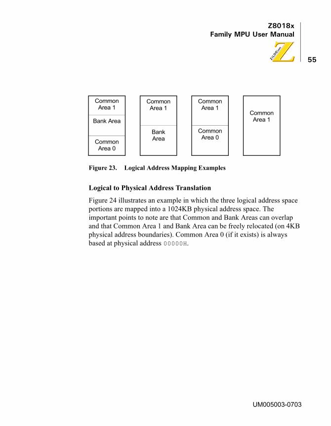
Z8018xFamily MPU User Manual
55
Figure 23. Logical Address Mapping Examples
Logical to Physical Address Translation
Figure 24 illustrates an example in which the three logical address space portions are mapped into a 1024KB physical address space. The important points to note are that Common and Bank Areas can overlap and that Common Area 1 and Bank Area can be freely relocated (on 4KB physical address boundaries). Common Area 0 (if it exists) is always based at physical address 00000H.
Common
Bank Area
Common
Common
Bank
Common
Common
Common
Area 1
Area 0
Area 1
Area 1
Area
Area 1
Area 0
UM005003-0703

Z8018xFamily MPU User Manual
56
Figure 24. Physical Address Transition
MMU Block Diagram
The MMU block diagram is depicted in Figure 25. The MMU translates internal 16-bit logical addresses to external 20-bit physical addresses.
Figure 25. MMU Block Diagram
Logical Address Space
Physical Address Space
Common Area 1
Bank Area
Common Area 0
Common Base
Bank Base
FFFFH
0000H
FFFFFH
00000H
0
+
+
+x y z
z
y
x
MMU Common/Bank AreaRegister; CBAR (8) Memory
Management
8PA12—PA19
LA12—LA154
MMU Common Base Register; CBR (8)MMU Bank Base Register; BBR (8)
LA: Logical AddressPA: Physical Address
Internal Address/Data Bus
Unit
UM005003-0703

Z8018xFamily MPU User Manual
57
Whether address translation (Figure 26) takes place depends on the type of CPU cycle as follows.
• Memory Cycles
Address Translation occurs for all memory access cycles including instruction and operand fetches, memory data reads and writes, hardware interrupt vector fetch, and software interrupt restarts.
• I/O Cycles
The MMU is logically bypassed for I/O cycles. The 16-bit logical I/O address space corresponds directly with the 16-bit physical I/O address space. The four high-order bits (A16–A19) of the physical address are always 0 during I/O cycles.
Figure 26. I/O Address Translation
• DMA Cycles
When the Z8X180 on-chip DMAC is using the external bus, the MMU is physically bypassed. The 20-bit source and destination registers in the DMAC are directly output on the physical address bus (A0–A19).
MMU Registers
Three MMU registers are used to program a specific configuration of logical and physical memory.
LA15
PA19
LA0
PA16 PA15 PA0
“0000” Logical Address
Physical Address
UM005003-0703

Z8018xFamily MPU User Manual
58
• MMU Common/Bank Area Register (CBAR)
• MMU Common Base Register (CBR)
• MMU Bank Base Register (BBR)
CBAR is used to define the logical memory organization, while CBR and BBR are used to relocate logical areas within the 1024KB physical address space. The resolution for both setting boundaries within the logical space and relocation within the physical space is 4KB.
The CA field of CBAR determines the start address of Common Area 1 (Upper Common) and by default, the end address of the Bank Area. The BA field determines the start address of the Bank Area and by default, the end address of Common Area 0 (Lower Common).
The CA and BA fields of CBAR may be freely programmed subject only to the restriction that CA may never be less than BA. Figures 27 and 28 illustrate examples of logical memory organizations associated with different values of CA and BA.
Figure 27. Logical Memory Organization
Common
Bank Area
Common
Common
Bank Area
Common
Common
Common
Common Area 1Lower Limit Address
>Bank Area
Lower Limit Address>
0000H
Common Area 1Lower lImit Address
>Bank Area
Lower lImit Address=
0000H
Common Area 1Lower Limit Address
=Bank Area
Lower Limit Address>
0000H
Common Area 1Lower Limit Address
=Bank Area
Lower Limit Address=
0000H(RESET Condition)
Area 1
Area 1
Area 0
Area 1Area 1
Area 0
UM005003-0703
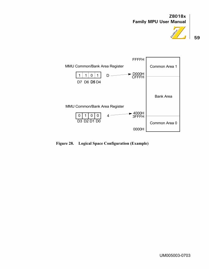
Z8018xFamily MPU User Manual
59
Figure 28. Logical Space Configuration (Example)
MMU Common/Bank Area Register
MMU Common/Bank Area Register
D7
FFFFH
D000HCFFFH
4000H3FFFH
0000H
D
4
D6 D5 D4
D3 D2 D1 D0
D5
1 1 0 1
0 1 0 0
Bank Area
Common Area 1
Common Area 0
UM005003-0703
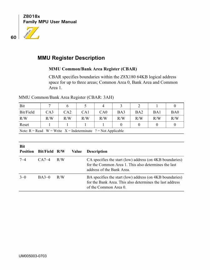
Z8018xFamily MPU User Manual
60
MMU Register Description
MMU Common/Bank Area Register (CBAR)
CBAR specifies boundaries within the Z8X180 64KB logical address space for up to three areas; Common Area 0, Bank Area and Common Area 1.
MMU Common/Bank Area Register (CBAR: 3AH)
Bit 7 6 5 4 3 2 1 0Bit/Field CA3 CA2 CA1 CA0 BA3 BA2 BA1 BA0R/W R/W R/W R/W R/W R/W R/W R/W R/WReset 1 1 1 1 0 0 0 0Note: R = Read W = Write X = Indeterminate ? = Not Applicable
BitPosition Bit/Field R/W Value Description
7–4 CA7–4 R/W CA specifies the start (low) address (on 4KB boundaries) for the Common Area 1. This also determines the last address of the Bank Area.
3–0 BA3–0 R/W BA specifies the start (low) address (on 4KB boundaries) for the Bank Area. This also determines the last address of the Common Area 0.
UM005003-0703

Z8018xFamily MPU User Manual
61
MMU Common Base Register (CBR)
CBR specifies the base address (on 4K boundaries) used to generate a 20-bit physical address for Common Area 1 accesses. All bits of CBR are reset to 0 during RESET.
MMU Common Base Register (CBR: 38H)
Bit 7 6 5 4 3 2 1 0Bit/Field CB7 CB6 CB5 CB4 CB3 CB2 CB1 CB0R/W R/W R/W R/W R/W R/W R/W R/W R/WReset 0 0 0 0 0 0 0 0Note: R = Read W = Write X = Indeterminate ? = Not Applicable
BitPosition Bit/Field R/W Value Description
7–0 CB7–0 R/W CBR specifies the base address (on 4KB boundaries) used to generate a 20-bit physical address for Common Area 1 accesses.
UM005003-0703

Z8018xFamily MPU User Manual
62
MMU Bank Base Register (BBR)
BBR specifies the base address (on 4KB boundaries) used to generate a 20-bit physical address for Bank Area accesses. All bits of BBR are reset to 0 during RESET.
Physical Address Translation
Figure 29 illustrates the way in which physical addresses are generated based on the contents of CBAR, CBR and BBR. MMU comparators classify an access by logical area as defined by CBAR. Depending on which of the three potential logical areas (Common Area 1, Bank Area, or Common Area 0) is being accessed, the appropriate 8- or 7-bit base address is added to the high-order 4 bits of the logical address, yielding a 19- or 20-bit physical address. CBR is associated with Common Area 1 accesses. Common Area 0, if defined, is always based at physical address 00000H.
MMU Bank Base Register (BBR: 39H)
Bit 7 6 5 4 3 2 1 0Bit/Field BB7 BB6 BB5 BB4 BB3 BB2 BB1 BB0R/W R/W R/W R/W R/W R/W R/W R/W R/WReset 0 0 0 0 0 0 0 0Note: R = Read W = Write X = Indeterminate ? = Not Applicable
BitPosition Bit/Field R/W Value Description
7–0 BB7–0 R/W BBR specifies the base address (on 4KB boundaries) used to generate a 20-bit physical address for Bank Area accesses.
UM005003-0703
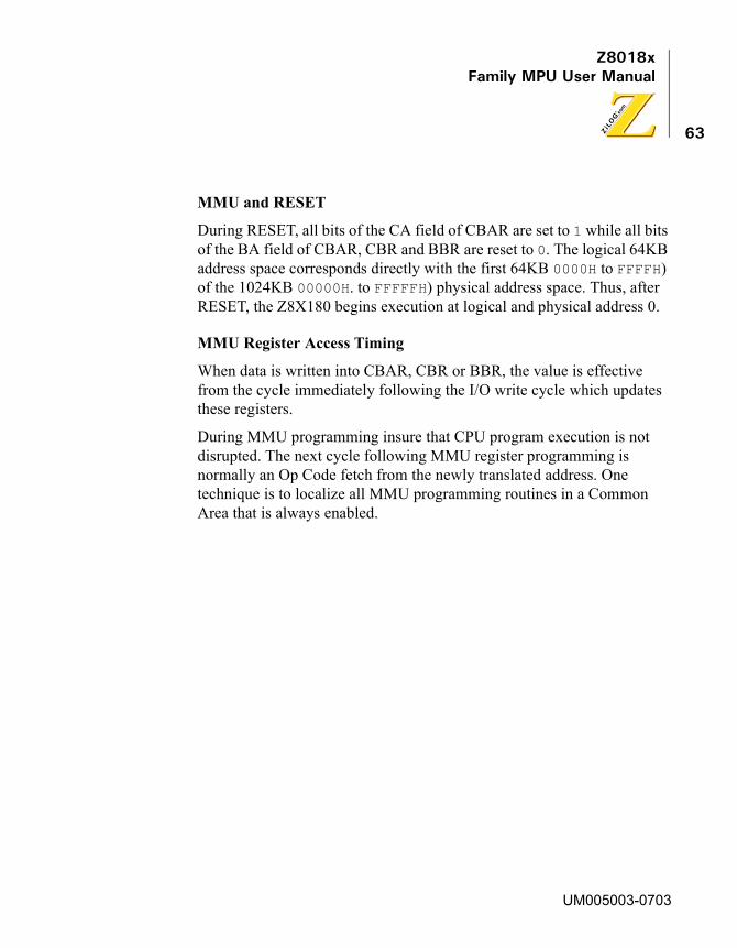
Z8018xFamily MPU User Manual
63
MMU and RESET
During RESET, all bits of the CA field of CBAR are set to 1 while all bits of the BA field of CBAR, CBR and BBR are reset to 0. The logical 64KB address space corresponds directly with the first 64KB 0000H to FFFFH) of the 1024KB 00000H. to FFFFFH) physical address space. Thus, after RESET, the Z8X180 begins execution at logical and physical address 0.
MMU Register Access Timing
When data is written into CBAR, CBR or BBR, the value is effective from the cycle immediately following the I/O write cycle which updates these registers.
During MMU programming insure that CPU program execution is not disrupted. The next cycle following MMU register programming is normally an Op Code fetch from the newly translated address. One technique is to localize all MMU programming routines in a Common Area that is always enabled.
UM005003-0703

Z8018xFamily MPU User Manual
64
Figure 29. Physical Address Generation
Figure 30. Physical Address Generation 2
Adder
Comparator
D3 — D0
D7 — D4
012 1115
8
4
4
4
MMU Common/Bank Area Register
MMU Common/
RegisterBank Area
MMU Common Base Reg.
MMU Bank Base Reg.
0 0 0 0 0 0 0 04
8
LogicalAddress(64K)
Physical
(512 k or 1 M)
(19) 18 12 11 0
Address
LogicalAddress
(64 k)
111215
(7) 4 3 0
(19) 18 16 15 12 11
Base Register(8 bit)
PhysicalAddress
0
0
(1 M)
UM005003-0703

Z8018xFamily MPU User Manual
65
Packages not containing an A19 pin or situations using TOUT instead of A18 yield an address capable of only addressing 512K of physical space.
InterruptsThe Z8X180 CPU has twelve interrupt sources, 4 external and 8 internal, with fixed priority. (Reference Figure 31.)
This section explains the CPU registers associated with interrupt processing, the TRAP interrupt, interrupt response modes, and the external interrupts. The detailed discussion of internal interrupt generation (except TRAP) is presented in the appropriate hardware section (that is, PRT, DMAC, ASCI, and CSI/O).
Figure 31. Interrupt Sources
Interrupt Control Registers and Flags. The Z8X180 has three registers and two flags which are associated with interrupt processing.
Note:
Higher Priority
Lower Priority
(1)(2)(3)(4)(5)(6)(7)(8)(9)
(10)(11)(12)
TRAP (Undefined Op Code Trap)NMI (Non Maskable Interrupt)INT0 (Maskable Interrupt Level 0)INT1 (Maskable Interrupt Level 1)INT2 (Maskable Interrupt Level 2)Timer 0Timer 1DMA channel 0DMA channel 1Clocked Serial I/O PortAsynchronous SCI channel 0Asynchronous SCI channel 1
Internal Interrupt
External Interrupt
Internal Interrupt
UM005003-0703

Z8018xFamily MPU User Manual
66
Interrupt Vector Register (I)
Mode 2 for INT0 external interrupt, INT1 and INT2 external interrupts, and all internal interrupts (except TRAP) use a programmable vectored technique to determine the address at which interrupt processing starts. In response to the interrupt a 16-bit address is generated. This address accesses a vector table in memory to obtain the address at which execution restarts.
While the method for generation of the least significant byte of the table address differs, all vectored interrupts use the contents of I as the most significant byte of the table address. By programming the contents of I, vector tables can be relocated on 256 byte boundaries throughout the 64KB logical address space.
I is read/written with the LD A, I and LD I, A instructions rather than I/O (IN, OUT) instructions. I is initialized to 00H during RESET.
Interrupt Vector Low Register
This register determines the most significant three bits of the low-order byte of the interrupt vector table address for external interrupts INT1 and INT2 and all internal interrupts (except TRAP). The five least significant bits are fixed for each specific interrupt source. By programming IL, the
Function Name Access Method
Interrupt Vector High I LD A,I and LD I, A instructions
Interrupt Vector Low IL I/O instruction (addr = 33H)
Interrupt/Trap Control ITC I/O instruction (addr = 34H)
Interrupt Enable Flag 1,2 IEF1, IEF2 El and DI
Note:
UM005003-0703
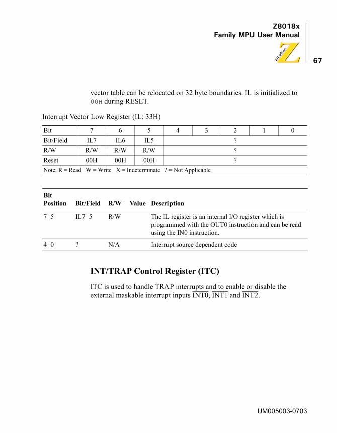
Z8018xFamily MPU User Manual
67
vector table can be relocated on 32 byte boundaries. IL is initialized to 00H during RESET.
INT/TRAP Control Register (ITC)
ITC is used to handle TRAP interrupts and to enable or disable the external maskable interrupt inputs INT0, INT1 and INT2.
Interrupt Vector Low Register (IL: 33H)
Bit 7 6 5 4 3 2 1 0Bit/Field IL7 IL6 IL5 ?R/W R/W R/W R/W ?
Reset 00H 00H 00H ?Note: R = Read W = Write X = Indeterminate ? = Not Applicable
BitPosition Bit/Field R/W Value Description
7–5 IL7–5 R/W The IL register is an internal I/O register which is programmed with the OUT0 instruction and can be read using the IN0 instruction.
4–0 ? N/A Interrupt source dependent code
UM005003-0703

Z8018xFamily MPU User Manual
68
Interrupt Enable Flag 1,2 (IEF1, IEF2)
IEF1 controls the overall enabling and disabling of all internal and external maskable interrupts (that is, all interrupts except NMI and TRAP.
INT/TRAP Control Register (ITC: 34H)
Bit 7 6 5 4 3 2 1 0Bit/Field TRAP UFO ? ITE2 ITE1 ITE0R/W R/W R N/A R/W R/W R/WReset 0 0 0 0 0 1Note: R = Read W = Write X = Indeterminate ? = Not Applicable
BitPosition Bit/Field R/W Value Description
7 TRAP R/W This bit is set to 1 when an undefined Op Code is fetched. TRAP can be reset under program control by writing it with 0, however, it cannot be written with 1 under program control.
6 UFO R Undefined Fetch Object (bit 6).When a TRAP interrupt occurs the contents of UFO allow determination of the starting address of the undefined instruction. This action is necessary since the TRAP may occur on either the second or third byte of the Op Code. UFO allows the stacked PC value to be correctly adjusted. If UFO = 0, the first Op Code should be interpreted as the stacked PC-1. If UFO = 1, the first Op Code address is stacked PC-2.
2–0 ITE2–0 R/W Interrupt Enable — ITE2, ITE1 and ITE0 enable and disable the external interrupt inputs INT2, INT1 and INT0, respectively. If reset to 0, the interrupt is masked.
UM005003-0703

Z8018xFamily MPU User Manual
69
If IEF1 is 0, all maskable interrupts are disabled. IEF1 can be reset to 0 by the DI (Disable Interrupts) instruction and set to 1 by the El (Enable Interrupts) instruction.
The purpose of IEF2 is to correctly manage the occurrence of NMI. During NMI, the prior interrupt reception state is saved and all maskable interrupts are automatically disabled (IEF1 copied to IEF2 and then IEF1 cleared to 0). At the end of the NMI interrupt service routine, execution of the RETN (Return from Non-maskable Interrupt) automatically restores the interrupt receiving state (by copying IEF2 to IEF1) prior to the occurrence of NMI.
Table 8 describes how the IEF2 state can be reflected in the P/V bit of the CPU Status Register by executing LD A, I or LD A, R instructions.
Table 8. State of IEF1 and IEF2
CPU Operation IEF1 IEF2 REMARKS
RESET 0 0 Inhibits the interrupt except NMI and TRAP.
NMI 0 IEF1 Copies the contents of IEF1 to IEF2
RETN IEF2 not affected Returns from the NMI service routine.
Interrupt except NMI end TRAP
0 0 Inhibits the interrupt except NMI end TRAP
RETI not affected not affected
TRAP not affected not affected
EI 1 1
UM005003-0703

Z8018xFamily MPU User Manual
70
TRAP Interrupt
The Z8X180 generates a non-maskable (not affected by the state of IEF1) TRAP interrupt when an undefined Op Code fetch occurs. This feature can be used to increase software reliability, implement an extended instruction set, or both. TRAP may occur during Op Code fetch cycles and also if an undefined Op Code is fetched during the interrupt acknowledge cycle for INT0 when Mode 0 is used.
When a TRAP interrupt occurs the Z8X180 operates as follows:
1. The TRAP bit in the Interrupt TRAP/Control (ITC) register is set to 1.
2. The current PC (Program Counter) value, reflecting location of the undefined Op Code, is saved on the stack.
3. The Z8X180 vectors to logical address 0. Note that if logical address 0000H is mapped to physical address 00000H. the vector is the same as for RESET. In this case, testing the TRAP bit in ITC reveals whether the restart at physical address 00000H was caused by RESET or TRAP.
The state of the UFO (Undefined Fetch Object) bit in ITC allows TRAP manipulation software to correctly adjust the stacked PC, depending on whether the second or third byte of the Op Code generated the TRAP. If UFO is 0, the starting address of the invalid instruction is equal to the
DI 0 0
LD A, I not affected not affected Transfers the contents of IEF1 to P/V
LID A, R not affected not affected Transfers the contents of IEF1 to P/V
Table 8. State of IEF1 and IEF2 (Continued)
CPU Operation IEF1 IEF2 REMARKS
UM005003-0703

Z8018xFamily MPU User Manual
71
stacked PC-1. If UFO is 1, the starting address of the invalid instruction is equal to the stacked PC-2.
Bus Release cycle, Refresh cycle, DMA cycle, and WAIT cycle cannot be inserted just after TTP state which is inserted for TRAP interrupt sequence. Figure depicts TRAP Timing - 2nd Op Code undefined and Figure illustrates Trap Timing - 3rd Op Code undefined.
Figure 32. TRAP Timing Diagram -2nd Op Code Undefined
2nd Op Code Fetch Cycle PC Stacking
Restart from 0000H
Op Code Fetch Cycle
PC SP-1 SP-2 0000H
Undefined Op Code
TiTi Ti T1Ti TiT1 T2 T3 T2 T3 T1 T2 T3 T1 T2 T3Phi
A0–A19
WR
RD
MREQ
D0–D7
MI
PCH PCL
UM005003-0703
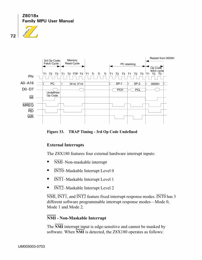
Z8018xFamily MPU User Manual
72
Figure 33. TRAP Timing - 3rd Op Code Undefined
External Interrupts
The Z8X180 features four external hardware interrupt inputs:
• NMI–Non-maskable interrupt
• INT0–Maskable Interrupt Level 0
• INT1–Maskable Interrupt Level 1
• INT2–Maskable Interrupt Level 2
NMI, INT1, and INT2 feature fixed interrupt response modes. INT0 has 3 different software programmable interrupt response modes—Mode 0, Mode 1 and Mode 2.
NMI - Non-Maskable Interrupt
The NMI interrupt input is edge-sensitive and cannot be masked by software. When NMI is detected, the Z8X180 operates as follows:
Phi
A0–A19
WRRD
MREQ
D0–D7
MI
TiT1 TiTiT1 T2 T3 T2T3 T1 T3T1 T2T3T1 T2 TTP T1 T2 T3
MemoryPC stacking
Restart from 0000H
Op Code fetch cycle
0000HSP-1 SP-2
PCLPCH
IX+d, IY+dPC
3rd Op Code Fetch Cycle
Undefined Op Code
Read Cycle
UM005003-0703

Z8018xFamily MPU User Manual
73
1. DMAC operation is suspended by the clearing of the DME (DMA Main Enable) bit in DCNTL.
2. The PC is pushed onto the stack.
3. The contents of IEF1 are copied to IEF2. This saves the interrupt reception state that existed prior to NMI.
4. IEF1 is cleared to 0. This disables all external and internal maskable interrupts (that is, all interrupts except NMI and TRAP).
5. Execution commences at logical address 0066H.
The last instruction of an NMI service routine must be RETN (Return from Non-maskable Interrupt). This restores the stacked PC, allowing the interrupted program to continue. Furthermore, RETN causes IEF2 to be copied to IEF1, restoring the interrupt reception state that existed prior to NMI.
NMI, because it can be accepted during Z8X180 on-chip DMAC operation, can be used to externally interrupt DMA transfer. The NMI service routine can reactivate or abort the DMAC operation as required by the application.
For NMI, take special care to insure that interrupt inputs do not overrun the NMI service routine. Unlimited NMI inputs without a corresponding number of RETN instructions eventually cause stack overflow.
Figure 34 depicts the use of NMI and RETN while Figure 35 details NMI response timing. NMI is edge sensitive and the internally latched NMI falling edge is held until it is sampled. If the falling edge of NMI is latched before the falling edge of the clock state prior to T3 or T1 in the last machine cycle, the internally latched NMI is sampled at the falling edge of the clock state prior to T3 or T1 in the last machine cycle and NMI acknowledge cycle begins at the end of the current machine cycle.
Note:
UM005003-0703

Z8018xFamily MPU User Manual
74
Figure 34. NMI Use
Main Program
NMI
EF1 0 PCH
EF1
PCL
PCL PCH
NMIInterrupt ServiceProgram
0066H
RETN
��� (SP-2)��� (SP-1)��� EF1��� EF2
� EF2� (SP)� (SP+1)
Phi
A0–A19
WR
RD
MREQ
D0–D7
MI
PCH PCL
Instruction
Last MC NMI acknowledge cycle
PC is pushed onto stack Restart from 0066H
Op Code fetch
PC SP-1 SP-2 0066H
NMI
T1 T3 Ti T1 T1 T2 T3 T1 T2 T3T1 T1 T2 T3
UM005003-0703

Z8018xFamily MPU User Manual
75
Figure 35. NMI Timing
INT0 - Maskable Interrupt Level 0
The next highest priority external interrupt after NMI is INT0. INT0 is sampled at the falling edge of the clock state prior to T3 or T1 in the last machine cycle. If INT0 is asserted LOW at the falling edge of the clock state prior to T3 or T1 in the last machine cycle, INT0 is accepted. The interrupt is masked if either the IEF1 flag or the ITEO (Interrupt Enable 0) bit in ITC are reset to 0. After RESET the state is as follows:
1. IEF1 is 0, so INT0 is masked
2. ITE0 is 1, so INT0 is enabled by execution of the El (Enable Interrupts) instruction
The INT0 interrupt is unique in that 3 programmable interrupt response modes are available - Mode 0, Mode 1 and Mode 2. The specific mode is selected with the IM 0, IM 1 and IM 2 (Set Interrupt Mode) instructions. During RESET, the Z8X180 is initialized to use Mode 0 for INT0. The 3 interrupt response modes for INT0 are:
• Mode 0–Instruction fetch from data bus
• Mode 1–Restart at logical address 0038H
• Mode 2–Low-byte vector table address fetch from data bus
INT0 Mode 0
During the interrupt acknowledge cycle, an instruction is fetched from the data bus (DO–D7) at the rising edge of T3. Often, this instruction is one of the eight single byte RST (RESTART) instructions which stack the PC and restart execution at a fixed logical address. However, multibyte instructions can be processed if the interrupt acknowledging device can provide a multibyte response. Unlike all other interrupts, the PC is not automatically stacked:
UM005003-0703

Z8018xFamily MPU User Manual
76
The TRAP interrupt occurs if an invalid instruction is fetched during Mode 0 interrupt acknowledge. (Reference Figure 36.)
Figure 36. INT0 Mode 0 Timing Diagram
INT0 Mode 1
When INT0 is received, the PC is stacked and instruction execution restarts at logical address 0038H. Both IEF1 and IEF2 flags are reset to 0,
Note:
Phi
A0–A19
WR
RD
MREQ
D0–D7
M1
IORQ
T1 T3Ti TiTWT2 T1 T2T3 T1T2 T3TW
PC is pushed onto stack
RST instruction executionINT0 acknowledge cycleLast MC
PC SP-1 SP-2
PCH PCL
RST instruction
MC: Machine Cycle*Two Wait States are automatically inserted
* *
INT0
UM005003-0703

Z8018xFamily MPU User Manual
77
disabling all maskable interrupts. The interrupt service routine normally terminates with the EI (Enable Interrupts) instruction followed by the RETI (Return from Interrupt) instruction, to reenable the interrupts. Figure 37 depicts the use of INT0 (Mode 1) and RETI for the Mode 1 interrupt sequence.
Figure 37. INT0 Mode 1 Interrupt Sequence
Figure 38 illustrates INT0 Mode 1 Timing.
INT0 (Mode 1)
Main Program
0 PCH PCL
PCL PCH
Interrupt ServiceProgram
0038H
RETI
���� (SP-2)����� (SP-1)����� EF1, EF2
���(SP)���(SP+1) E1 (1 � 1EF1, 1EF2)
INT0 (Mode 1)
UM005003-0703
Z8018xFamily MPU User Manual
78
Figure 38. INT0 Mode 1 Timing
INT0 Mode 2
This method determines the restart address by reading the contents of a table residing in memory. The vector table consists of up to 128 two-byte restart addresses stored in low byte, high byte order.
Phi
A0–A19
WR
RD
MREQ
D0–D7
M1
PCH PCL
PC SP-1 SP-2 0038H
INT0
T1 T3TW* T2T1T2 T3 T1T2 T3 T1T2 T3TW*
Last MC
PC is pushed onto stack
Op Code Fetch CycleINT0 Acknowledge Cycle
*Two Wait States are automatically inserted
ST
IORQ
UM005003-0703
Z8018xFamily MPU User Manual
79
The vector table address is located on 256 byte boundaries in the 64KB logical address space programmed in the 8-bit Interrupt Vector Register (1). Figure 39 depicts the INT0 Mode 2 Vector acquisition.
Figure 39. INT0 Mode 2 Vector Acquisition
During the INT0 Mode 2 acknowledge cycle, the low-order 8 bits of the vector is fetched from the data bus at the rising edge of T3 and the CPU acquires the 16-bit vector.
Next, the PC is stacked. Finally, the 16-bit restart address is fetched from the vector table and execution begins at that address.
External vector acquisition is indicated by both MI and IORQ LOW. Two Wait States (TW) are automatically inserted for external vector fetch cycles.
During RESET the Interrupt Vector Register (I) is initialized to 00H and, if necessary, should be set to a different value prior to the occurrence of a Mode 2 INT0 interrupt. Figure illustrates INT0 interrupt Mode 2 Timing.
Vector + 1
Vector
Memory
256 BytesVectorTable
16-bit Vector
Offset
Interrupt Vector Register I
8-bit on Data Bus
High-order 8 bits
Low-order 8 bits of starting address
of starting address
Note:
UM005003-0703
Z8018xFamily MPU User Manual
80
Figure 40. INT0 Interrupt Mode 2 Timing Diagram
INT1, INT2
The operation of external interrupts INT1 and INT2 is a vector mode similar to INT0 Mode 2. The difference is that INT1 and INT2 generate the low-order byte of vector table address using the IL (Interrupt Vector Low) register rather than fetching it from the data bus. This difference is
A0–A19
WR
RD
MREQ
D0–D7
M1
PC SP-1 SP-2
INT0
T1 T3TW* T2TiT2 T1T3 T1T2 T3TW*
*Two Wait States are automatically inserted
ST
IORQ
Vector Vector+1
Vector Lower Address Read PC is pushed onto stack
Interrupt
Op Code
T1 T1 T1T2 T3 T2T2 T3
Starting address
PCH PCL
Starting Address Starting Address (Upper Address)(Lower Address)Lower Vector
Phi
ManipulationCycle
Fetch CycleINT0 Acknowledge CycleLast MC
UM005003-0703
Z8018xFamily MPU User Manual
81
UM005003-0703
also the interrupt response sequence used for all internal interrupts (except TRAP).
As depicted in Figure 41, the low-order byte of the vector table address has the most significant three bits of the software programmable IL register while the least significant five bits are a unique fixed value for each interrupt (INT1, INT2 and internal) source:
Figure 41. INT1, INT2 Vector Acquisition
INT1 and INT2 are globally masked by IEF1 is 0. Each is also individually maskable by respectively clearing the ITE1 and ITE2 (bits 1,2) of the INT/TRAP control register to 0.
During RESET, IEF1, ITE1 and ITE2 bits are reset to 0.
Internal Interrupts
Internal interrupts (except TRAP) use the same vectored response mode as INT1 and INT2. Internal interrupts are globally masked by IEF1 is 0. Individual internal interrupts are enabled/disabled by programming each
Vector + 1
Vector
32 BytesVectorTable
16-bit Vector
High-order 8 bits
Low-order 8 bits of starting address
of starting address
I IL Fixed Code (5 bits)
Memory

Z8018xFamily MPU User Manual
82
individual I/O (PRT, DMAC, CSI/O, ASCI) control register. The lower vector of INT1 INT2 and internal interrupt are summarized in Table 9.
Interrupt Acknowledge Cycle TimingsFigure 43 illustrates INT1, INT2, and internal interrupts timing. INT1 and INT2 are sampled at the falling edge of the clock state prior to T2 or T1 in the last machine cycle. If INT1 or INT2 is asserted Low at the falling edge of clock state prior to T3 or T1 in the last machine cycle, the interrupt request is accepted.
Table 9. Vector Table
Interrupt Source Priority
IL Fixed Code
b7 b6 b5 b4 b3 b2 b1 b0
INT1 — — — 0 0 0 0 0
INT2 — — — 0 0 0 1 0
PRT channel 0 — — — 0 0 1 0 0
PRT channel 1 — — — 0 0 1 1 0
DMA channel 0 — — — 0 1 0 0 0
DMA channel 1 — — — 0 1 0 1 0
CSI/O — — — 0 1 1 0 0
ASCI channel 0 — — — 0 1 1 1 0
ASCI channel 1 — — — 1 0 0 0 0
Highest
Lowest
UM005003-0703
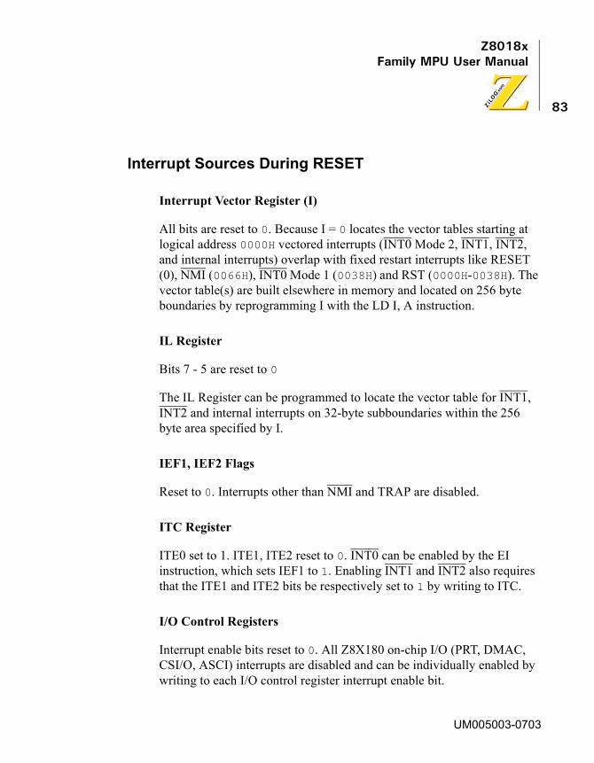
Z8018xFamily MPU User Manual
83
Interrupt Sources During RESET
Interrupt Vector Register (I)
All bits are reset to 0. Because I = 0 locates the vector tables starting at logical address 0000H vectored interrupts (INT0 Mode 2, INT1, INT2, and internal interrupts) overlap with fixed restart interrupts like RESET (0), NMI (0066H), INT0 Mode 1 (0038H) and RST (0000H-0038H). The vector table(s) are built elsewhere in memory and located on 256 byte boundaries by reprogramming I with the LD I, A instruction.
IL Register
Bits 7 - 5 are reset to 0
The IL Register can be programmed to locate the vector table for INT1, INT2 and internal interrupts on 32-byte subboundaries within the 256 byte area specified by I.
IEF1, IEF2 Flags
Reset to 0. Interrupts other than NMI and TRAP are disabled.
ITC Register
ITE0 set to 1. ITE1, ITE2 reset to 0. INT0 can be enabled by the EI instruction, which sets IEF1 to 1. Enabling INT1 and INT2 also requires that the ITE1 and ITE2 bits be respectively set to 1 by writing to ITC.
I/O Control Registers
Interrupt enable bits reset to 0. All Z8X180 on-chip I/O (PRT, DMAC, CSI/O, ASCI) interrupts are disabled and can be individually enabled by writing to each I/O control register interrupt enable bit.
UM005003-0703
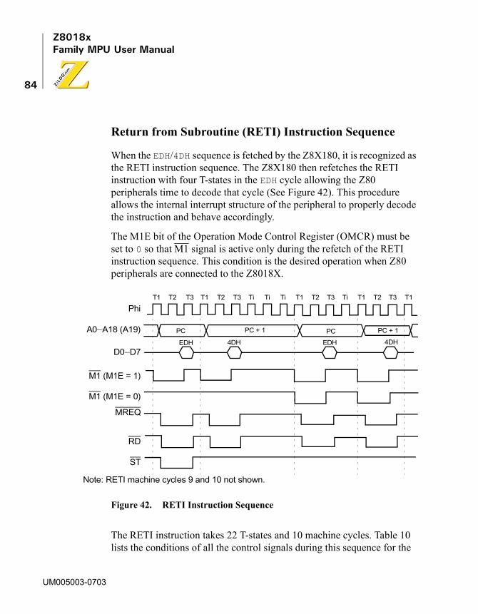
Z8018xFamily MPU User Manual
84
Return from Subroutine (RETI) Instruction Sequence
When the EDH/4DH sequence is fetched by the Z8X180, it is recognized as the RETI instruction sequence. The Z8X180 then refetches the RETI instruction with four T-states in the EDH cycle allowing the Z80 peripherals time to decode that cycle (See Figure 42). This procedure allows the internal interrupt structure of the peripheral to properly decode the instruction and behave accordingly.
The M1E bit of the Operation Mode Control Register (OMCR) must be set to 0 so that M1 signal is active only during the refetch of the RETI instruction sequence. This condition is the desired operation when Z80 peripherals are connected to the Z8018X.
Figure 42. RETI Instruction Sequence
The RETI instruction takes 22 T-states and 10 machine cycles. Table 10 lists the conditions of all the control signals during this sequence for the
RD
MREQ
D0–D7
T1
ST
PhiT3 Ti Ti Ti T1 T2 T3 Ti T1 T2 T3 T1T3 T1 T2T2
PC PC + 1 PC PC + 1
4DH4DHEDH EDH
M1 (M1E = 0)
M1 (M1E = 1)
A0–A18 (A19)
Note: RETI machine cycles 9 and 10 not shown.
UM005003-0703
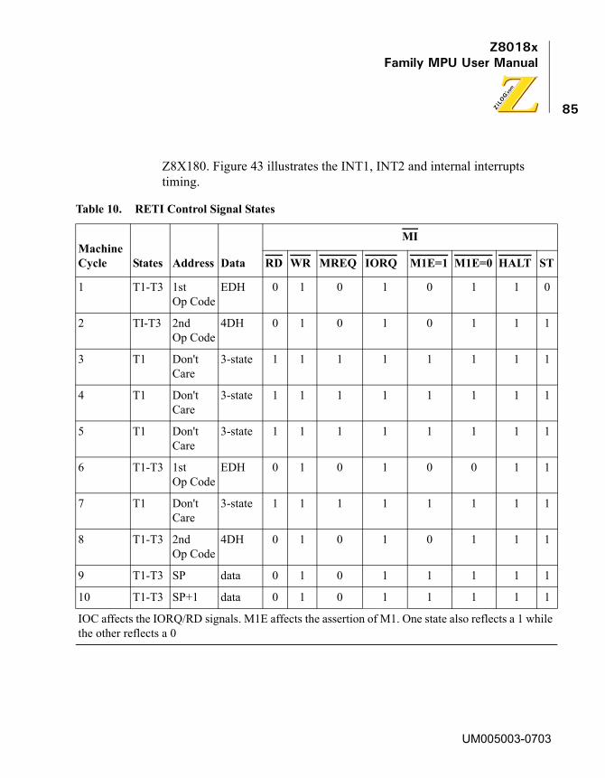
Z8018xFamily MPU User Manual
85
Z8X180. Figure 43 illustrates the INT1, INT2 and internal interrupts timing.
Table 10. RETI Control Signal States
MachineCycle States Address Data
MI
RD WR MREQ IORQ M1E=1 M1E=0 HALT ST
1 T1-T3 1stOp Code
EDH 0 1 0 1 0 1 1 0
2 TI-T3 2ndOp Code
4DH 0 1 0 1 0 1 1 1
3 T1 Don't Care
3-state 1 1 1 1 1 1 1 1
4 T1 Don't Care
3-state 1 1 1 1 1 1 1 1
5 T1 Don't Care
3-state 1 1 1 1 1 1 1 1
6 T1-T3 1stOp Code
EDH 0 1 0 1 0 0 1 1
7 T1 Don't Care
3-state 1 1 1 1 1 1 1 1
8 T1-T3 2ndOp Code
4DH 0 1 0 1 0 1 1 1
9 T1-T3 SP data 0 1 0 1 1 1 1 1
10 T1-T3 SP+1 data 0 1 0 1 1 1 1 1
IOC affects the IORQ/RD signals. M1E affects the assertion of M1. One state also reflects a 1 while the other reflects a 0
UM005003-0703
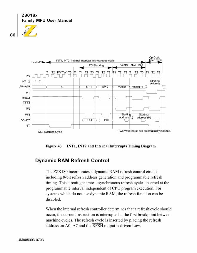
Z8018xFamily MPU User Manual
86
Figure 43. INT1, INT2 and Internal Interrupts Timing Diagram
Dynamic RAM Refresh Control
The Z8X180 incorporates a dynamic RAM refresh control circuit including 8-bit refresh address generation and programmable refresh timing. This circuit generates asynchronous refresh cycles inserted at the programmable interval independent of CPU program execution. For systems which do not use dynamic RAM, the refresh function can be disabled.
When the internal refresh controller determines that a refresh cycle should occur, the current instruction is interrupted at the first breakpoint between machine cycles. The refresh cycle is inserted by placing the refresh address on A0–A7 and the RFSH output is driven Low.
T1T1T1T1T1 T1 T2T2 T2 T2 T2TW* T3 T3 T3 T3 T3 T3T2TW* Ti
PC Stacking Vector Table Read
Op Codefetch cycleINT1, INT2, internal interrupt acknowledge cycleLast MC
INT1,2
A0–A19
M1
MREQ
IORQ
RD
WR
PC SP-1 SP-2 Vector Vector+1
Starting Address
Starting Starting
* Two Wait States are automatically inserted.
D0–D7
ST
MC: Machine Cycle
PCLPCH
Phi
address (L) address (H)
UM005003-0703

Z8018xFamily MPU User Manual
87
Refresh cycles may be programmed to be either two or three clock cycles in duration by programming the REFW (Refresh Wait) bit in the Refresh Control Register (RCR). The external WAIT input and the internal Wait State generator are not effective during refresh.
Figure 44 depicts the timing of a refresh cycle with a refresh wait (TRW) cycle.
Figure 44. Refresh Cycle Timing Diagram
NOTE: * If three refresh cycles are specified, TRW is inserted.Otherwise, TRW is not inserted
MC: Machine Cycle
MCi Refresh cycle MCi+1
TR1 TRW* TR2
Refresh signal(Internal signal)
Refresh address A0 — A7
MREQ
RFSH
UM005003-0703

Z8018xFamily MPU User Manual
88
Refresh Control Register (RCR)
The RCR specifies the interval and length of refresh cycles, while enabling or disabling the refresh function.
Refresh Control Register (RCR: 36H)
Bit 7 6 5 4 3 2 1 0Bit/Field REFE REFW ? CYC1 CYC0R/W R/W R/W ? R/W R/WReset 1 1 ? 0 0Note: R = Read W = Write X = Indeterminate ? = Not Applicable
BitPosition Bit/Field R/W Value Description
7 REFE R/W01
REFE: Refresh EnableDisables the refresh controllerEnables refresh cycle insertion.
6 REFW R/W01
Refresh Wait (bit 6)Causes the refresh cycle to be two clocks in duration.Causes the refresh cycle to be three clocks in duration by adding a refresh wait cycle (TRW).
1–0 CYC1–0 R/W Cycle Interval — CYC1 and CYC0 specify the interval (in clock cycles) between refresh cycles. In the case of dynamic RAMs requiring 128 refresh cycles every 2 ms (or 256 cycles in every 4 ms), the required refresh interval is less than or equal to 15.625 �s. Thus, the underlined values indicate the best refresh interval depending on CPU clock frequency. CYC0 and CYC1 are cleared to 0 during RESET. Refer to Table 11.
UM005003-0703
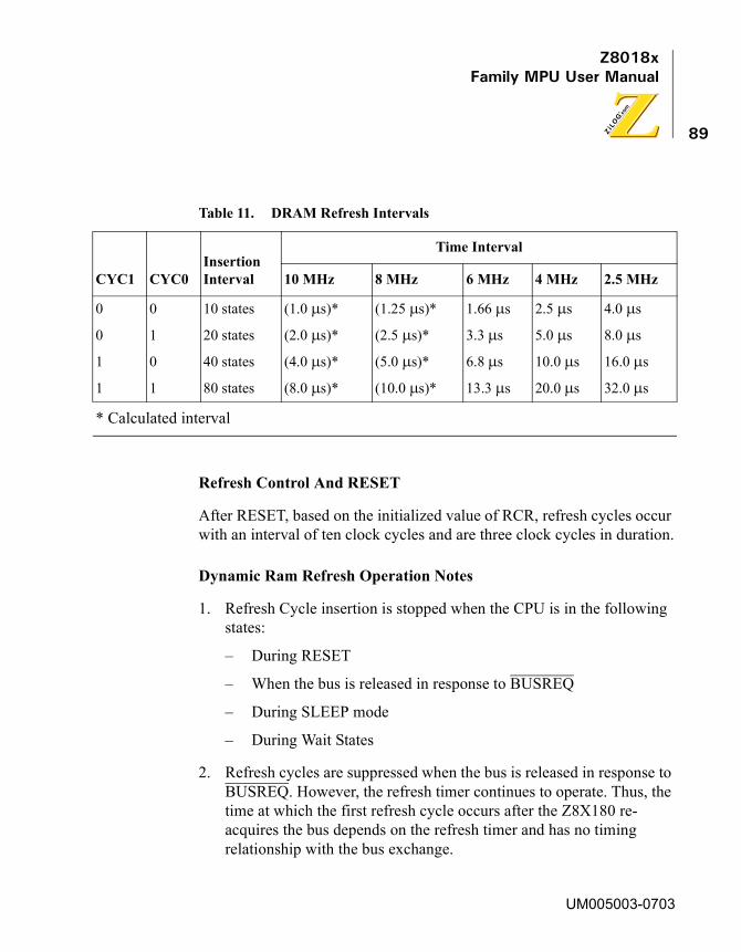
Z8018xFamily MPU User Manual
89
Refresh Control And RESET
After RESET, based on the initialized value of RCR, refresh cycles occur with an interval of ten clock cycles and are three clock cycles in duration.
Dynamic Ram Refresh Operation Notes
1. Refresh Cycle insertion is stopped when the CPU is in the following states:
– During RESET
– When the bus is released in response to BUSREQ
– During SLEEP mode
– During Wait States
2. Refresh cycles are suppressed when the bus is released in response to BUSREQ. However, the refresh timer continues to operate. Thus, the time at which the first refresh cycle occurs after the Z8X180 re-acquires the bus depends on the refresh timer and has no timing relationship with the bus exchange.
Table 11. DRAM Refresh Intervals
CYC1 CYC0InsertionInterval
Time Interval
10 MHz 8 MHz 6 MHz 4 MHz 2.5 MHz
0 0 10 states (1.0 �s)* (1.25 �s)* 1.66 �s 2.5 �s 4.0 �s
0 1 20 states (2.0 �s)* (2.5 �s)* 3.3 �s 5.0 �s 8.0 �s
1 0 40 states (4.0 �s)* (5.0 �s)* 6.8 �s 10.0 �s 16.0 �s
1 1 80 states (8.0 �s)* (10.0 �s)* 13.3 �s 20.0 �s 32.0 �s
* Calculated interval
UM005003-0703

Z8018xFamily MPU User Manual
90
3. Refresh cycles are suppressed during SLEEP mode. If a refresh cycle is requested during SLEEP mode, the refresh cycle request is internally latched (until replaced with the next refresh request). The latched refresh cycle is inserted at the end of the first machine cycle after SLEEP mode is exited. After this initial cycle, the time at which the next refresh cycle occurs depends on the refresh time and has no timing relationship with the exit from SLEEP mode.
4. Regarding (2) and (3), the refresh address is incremented by one for each successful refresh cycle, not for each refresh request. Thus, independent of the number of missed refresh requests, each refresh bus cycle uses a refresh address incremented by one from that of the previous refresh bus cycles.
DMA Controller (DMAC)The Z8X180 contains a two-channel DMA (Direct Memory Access) controller which supports high speed data transfer. Both channels (channel 0 and channel 1) feature the following capabilities:
• Memory Address Space
Memory source and destination addresses can be directly specified anywhere within the 1024KB physical address space using 20-bit source and destination memory addresses. In addition, memory transfers can arbitrarily cross 64KB physical address boundaries without CPU intervention.
• I/O Address Space
I/O source and destination addresses can be directly specified anywhere within the 64KB I/O address space (16-bit source and destination I/O addresses).
• Transfer Length
Up to 64KB are transferred based on a 16- bit byte count register.
UM005003-0703

Z8018xFamily MPU User Manual
91
• DREQ Input
Level- and edge-sense DREQ input detection are selectable.
TEND Output Used to indicate DMA completion to external devices.
• Transfer Rate
Each byte transfer occurs every 6 clock cycles. Wait States can be inserted in DMA cycles for slow memory or I/O devices. At the system clock (�) = 6 MHz, the DMA transfer rate is as high as 1.0 megabytes/second (no Wait States).
There is an additional feature disc for DMA interrupt request by DMA END. Each channel has the following additional specific capabilities:
Channel 0
• Memory to memory
• Memory to I/O
• Memory to memory mapped I/O transfers.
• Memory address increment, decrement, no-change
• Burst or cycle steal memory to/from memory transfers
• DMA to/from both ASCI channels
• Higher priority than DMAC channel 1
Channel 1
• Memory to/from I/O transfer
• Memory address increment, decrement
DMAC Registers
Each channel of the DMAC (channel 0, 1) contains three registers specifically associated with that channel.
UM005003-0703
Z8018xFamily MPU User Manual
92
Channel 0
• SAR0–Source Address Register
• DAR0–Destination Address Register
• BCR0–Byte Count Register
Channel 1
• MAR1–Memory Address Register
• IAR1–I/O Address Register
• BCR1–Byte Count Register
The two channels share the following three additional registers in common:
• DSTAT–DMA Status Register
• DMODE–DMA Mode Register
• DCNTL–DMA Control Register
DMAC Block Diagram
Figure 45 depicts the Z8X180 DMAC Block Diagram.
UM005003-0703
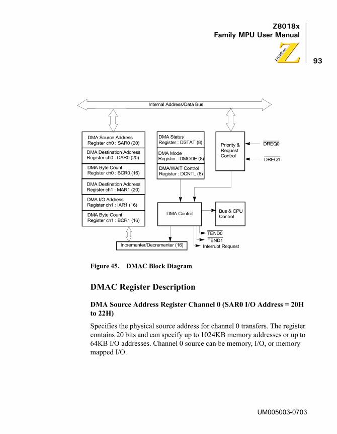
Z8018xFamily MPU User Manual
93
Figure 45. DMAC Block Diagram
DMAC Register Description
DMA Source Address Register Channel 0 (SAR0 I/O Address = 20H to 22H)
Specifies the physical source address for channel 0 transfers. The register contains 20 bits and can specify up to 1024KB memory addresses or up to 64KB I/O addresses. Channel 0 source can be memory, I/O, or memory mapped I/O.
Internal Address/Data Bus
Incrementer/Decrementer (16)
DMA Control Bus & CPUControl
TEND0TEND1
Interrupt Request
DREQ0
DREQ1
DMA StatusRegister : DSTAT (8)
DMA ModeRegister : DMODE (8)
DMA/WAIT ControlRegister : DCNTL (8)
Priority &RequestControl
DMA Source AddressRegister ch0 : SAR0 (20)
DMA Destination AddressRegister ch0 : DAR0 (20)
DMA Byte CountRegister ch0 : BCR0 (16)
DMA Destination AddressRegister ch1 : MAR1 (20)
DMA I/O AddressRegister ch1 : IAR1 (16)
DMA Byte CountRegister ch1 : BCR1 (16)
UM005003-0703
Z8018xFamily MPU User Manual
94
DMA Destination Address Register Channel 0 (DAR0 I/O Address = 23H to 25H)
Specifies the physical destination address for channel 0 transfers. The register contains 20 bits and can specify up to 1024KB memory addresses or up to 64KB I/O addresses. Channel 0 destination can be memory, I/O, or memory mapped I/O.
DMA Byte Count Register Channel 0 (BCR0 I/O Address = 26H to 27H)
Specifies the number of bytes to be transferred. This register contains 16 bits and may specify up to 64KB transfers. When one byte is transferred, the register is decremented by one. If n bytes are transferred, n is stored before the DMA operation.
DMA Memory Address Register Channel 1 (MAR1: I/O Address = 28H to 2AH)
Specifies the physical memory address for channel 1 transfers. This address may be a destination or source memory address. The register contains 20 bits and may specify up to 1024KB memory address.
DMA I/O Address Register Channel 1 (IAR1: I/O Address = 2BH to 2CH)
Specifies the I/O address for channel 1 transfers. This address may be a destination or source I/O address. The register contains 16 bits and may specify up to 64KB I/O addresses.
DMA Byte Count Register Channel 1 (BCR1: I/O Address = 2EH to 2FH)
Specifies the number of bytes to be transferred. This register contains 16 bits and may specify up to 64KB transfers. When one byte is transferred, the register is decremented by one.
UM005003-0703
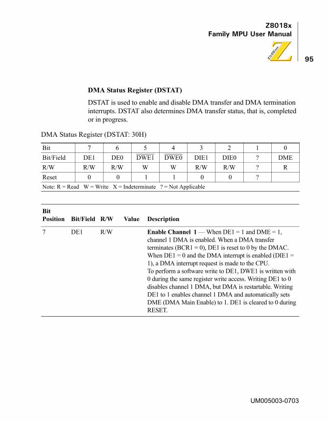
Z8018xFamily MPU User Manual
95
DMA Status Register (DSTAT)
DSTAT is used to enable and disable DMA transfer and DMA termination interrupts. DSTAT also determines DMA transfer status, that is, completed or in progress.
DMA Status Register (DSTAT: 30H)
Bit 7 6 5 4 3 2 1 0Bit/Field DE1 DE0 DWE1 DWE0 DIE1 DIE0 ? DMER/W R/W R/W W W R/W R/W ? RReset 0 0 1 1 0 0 ? Note: R = Read W = Write X = Indeterminate ? = Not Applicable
BitPosition Bit/Field R/W Value Description
7 DE1 R/W Enable Channel 1 — When DE1 = 1 and DME = 1, channel 1 DMA is enabled. When a DMA transfer terminates (BCR1 = 0), DE1 is reset to 0 by the DMAC. When DE1 = 0 and the DMA interrupt is enabled (DIE1 = 1), a DMA interrupt request is made to the CPU.To perform a software write to DE1, DWE1 is written with 0 during the same register write access. Writing DE1 to 0 disables channel 1 DMA, but DMA is restartable. Writing DE1 to 1 enables channel 1 DMA and automatically sets DME (DMA Main Enable) to 1. DE1 is cleared to 0 during RESET.
UM005003-0703

Z8018xFamily MPU User Manual
96
6 DE0 R/W Enable Channel 0 — When DE0 = 1 and DME = 1, channel 0 DMA is enabled. When a DMA transfer terminates BCR0 = 0), DE0: is reset to 0 by the DMAC. When DE0 = 0 and the DMA interrupt is enabled (DIE0 = 1), a DMA interrupt request is made to the CPU.To perform a software write to DE0, DWE0 must be written with 0 during the same register write access. Writing DE0 to 0 disables channel 0 DMA. Writing DE0 to 1 enables channel 0 DMA and automatically sets DME (DMA Main Enable) to 1. DE0 is cleared to 0 during RESET.
5 DWE1 W Bit Write Enable 1 — When performing any software write to DEI, DWE1 must be written with 0 during the same access. DWE1 write value of 0 is not held and DWE1 is always read as 1.
4 DWE0 W Bit Write Enable 0 — When performing any software write to DE0, DWE0 must be written with 0 during the same access. DWE0 write value of 0 is not held and DWE0 is always read as 1.
3 DIE1 R/W DMA Interrupt Enable Channel 1 — When DIE1 is set to 1, the termination channel 1 DMA transfer (indicated when DE1 is 0) causes a CPU interrupt request to be generated. When DIE1 is 0, the channel 1 DMA termination interrupt is disabled. DIE1 is cleared to 0 during RESET.
2 DIE0 DMA Interrupt Enable Channel 0 — When DIE0 is set to 1, the termination channel 0 of DMA transfer (indicated when DE0 is 0) causes a CPU interrupt request to be generated. When DIE0 is 0, the channel 0 DMA termination interrupt is disabled. DIE0 is cleared to 0 during RESET.
BitPosition Bit/Field R/W Value Description
UM005003-0703
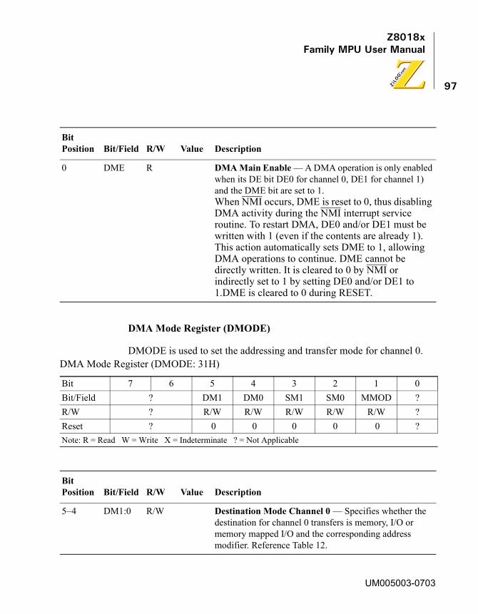
Z8018xFamily MPU User Manual
97
DMA Mode Register (DMODE)
DMODE is used to set the addressing and transfer mode for channel 0.
0 DME R DMA Main Enable — A DMA operation is only enabled when its DE bit DE0 for channel 0, DE1 for channel 1) and the DME bit are set to 1. When NMI occurs, DME is reset to 0, thus disabling DMA activity during the NMI interrupt service routine. To restart DMA, DE0 and/or DE1 must be written with 1 (even if the contents are already 1). This action automatically sets DME to 1, allowing DMA operations to continue. DME cannot be directly written. It is cleared to 0 by NMI or indirectly set to 1 by setting DE0 and/or DE1 to 1.DME is cleared to 0 during RESET.
DMA Mode Register (DMODE: 31H)
Bit 7 6 5 4 3 2 1 0Bit/Field ? DM1 DM0 SM1 SM0 MMOD ?R/W ? R/W R/W R/W R/W R/W ?Reset ? 0 0 0 0 0 ?Note: R = Read W = Write X = Indeterminate ? = Not Applicable
BitPosition Bit/Field R/W Value Description
5–4 DM1:0 R/W Destination Mode Channel 0 — Specifies whether the destination for channel 0 transfers is memory, I/O or memory mapped I/O and the corresponding address modifier. Reference Table 12.
BitPosition Bit/Field R/W Value Description
UM005003-0703
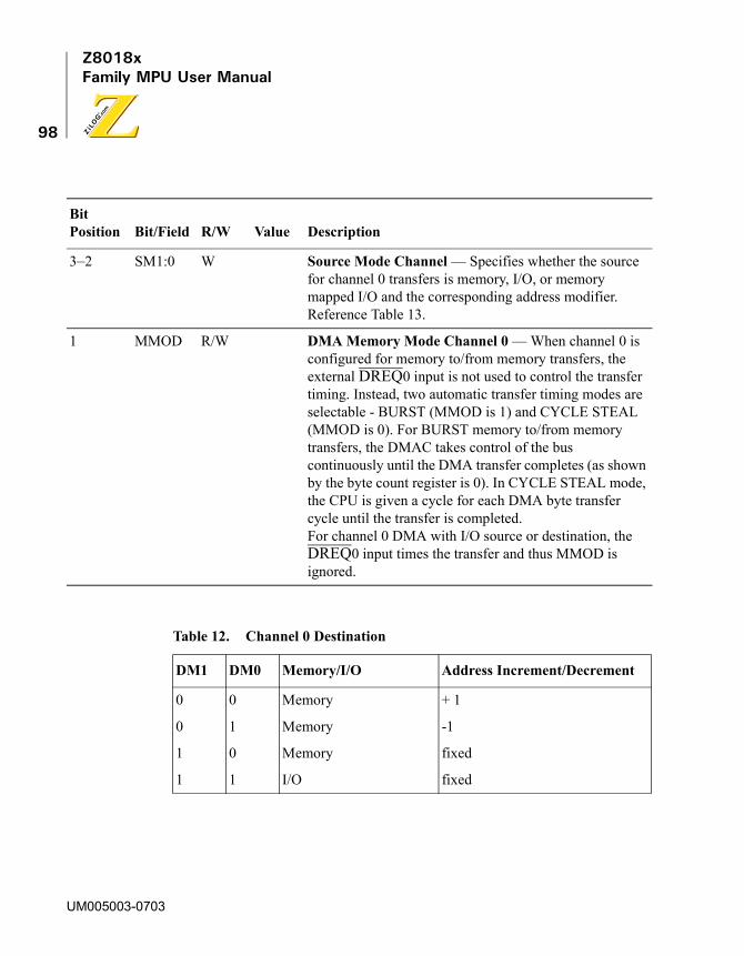
Z8018xFamily MPU User Manual
98
3–2 SM1:0 W Source Mode Channel — Specifies whether the source for channel 0 transfers is memory, I/O, or memory mapped I/O and the corresponding address modifier. Reference Table 13.
1 MMOD R/W DMA Memory Mode Channel 0 — When channel 0 is configured for memory to/from memory transfers, the external DREQ0 input is not used to control the transfer timing. Instead, two automatic transfer timing modes are selectable - BURST (MMOD is 1) and CYCLE STEAL (MMOD is 0). For BURST memory to/from memory transfers, the DMAC takes control of the bus continuously until the DMA transfer completes (as shown by the byte count register is 0). In CYCLE STEAL mode, the CPU is given a cycle for each DMA byte transfer cycle until the transfer is completed.For channel 0 DMA with I/O source or destination, the DREQ0 input times the transfer and thus MMOD is ignored.
Table 12. Channel 0 Destination
DM1 DM0 Memory/I/O Address Increment/Decrement
0 0 Memory + 1
0 1 Memory -1
1 0 Memory fixed
1 1 I/O fixed
BitPosition Bit/Field R/W Value Description
UM005003-0703
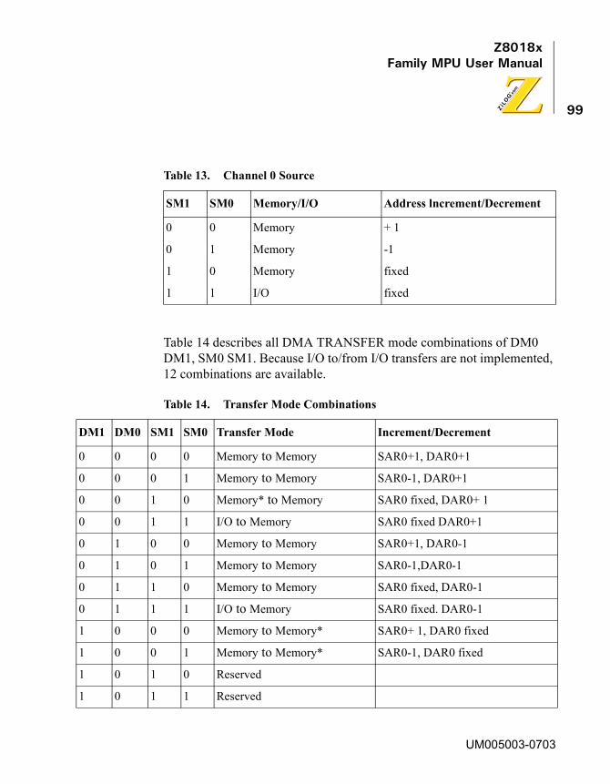
Z8018xFamily MPU User Manual
99
Table 14 describes all DMA TRANSFER mode combinations of DM0 DM1, SM0 SM1. Because I/O to/from I/O transfers are not implemented, 12 combinations are available.
Table 13. Channel 0 Source
SM1 SM0 Memory/I/O Address lncrement/Decrement
0 0 Memory + 1
0 1 Memory -1
1 0 Memory fixed
1 1 I/O fixed
Table 14. Transfer Mode Combinations
DM1 DM0 SM1 SM0 Transfer Mode Increment/Decrement
0 0 0 0 Memory�to Memory SAR0+1, DAR0+1
0 0 0 1 Memory�to Memory SAR0-1, DAR0+1
0 0 1 0 Memory*�to Memory SAR0 fixed, DAR0+ 1
0 0 1 1 I/O�to Memory SAR0 fixed DAR0+1
0 1 0 0 Memory�to Memory SAR0+1, DAR0-1
0 1 0 1 Memory�to Memory SAR0-1,DAR0-1
0 1 1 0 Memory�to Memory SAR0 fixed, DAR0-1
0 1 1 1 I/O�to Memory SAR0 fixed. DAR0-1
1 0 0 0 Memory�to Memory* SAR0+ 1, DAR0 fixed
1 0 0 1 Memory�to Memory* SAR0-1, DAR0 fixed
1 0 1 0 Reserved
1 0 1 1 Reserved
UM005003-0703

Z8018xFamily MPU User Manual
100
DMA/WAIT Control Register (DCNTL)
DCNTL controls the insertion of Wait States into DMAC (and CPU) accesses of memory or I/O Also, the DMA request mode for each DREQ DREQ0 and DREQ1) input is defined as level or edge sense. DCNTL also sets the DMA transfer mode for channel 1, which is limited to memory to/from I/O transfers.
1 1 0 0 Memory�to I/O SAR0+1, DAR0 fixed
1 1 0 1 Memory to I/O SAR0-1, DAR0 fixed
1 1 1 0 Reserved
1 1 1 1 Reserved
Note: *: includes memory mapped I/O.
Table 14. Transfer Mode Combinations
DM1 DM0 SM1 SM0 Transfer Mode Increment/Decrement
UM005003-0703
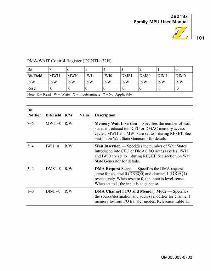
Z8018xFamily MPU User Manual
101
DMA/WAIT Control Register (DCNTL: 32H)
Bit 7 6 5 4 3 2 1 0Bit/Field MWI1 MWI0 IWI1 IWI0 DMS1 DMS0 DIM1 DIM0R/W R/W R/W R/W R/W R/W R/W R/W R/WReset 0 0 0 0 0 0 0 0Note: R = Read W = Write X = Indeterminate ? = Not Applicable
BitPosition Bit/Field R/W Value Description
7–6 MWI1–0 R/W Memory Wait Insertion —Specifies the number of wait states introduced into CPU or DMAC memory access cycles. MWI1 and MWI0 are set to 1 during RESET. See section on Wait State Generator for details.
5–4 IWI1–0 R/W Wait Insertion — Specifies the number of Wait States introduced into CPU or DMAC I/O access cycles. IWI1 and IWI0 are set to 1 during RESET. See section on Wait State Generator for details.
3–2 DMS1–0 R/W DMA Request Sense — Specifies the DMA request sense for channel 0 (DREQ0) and channel 1 (DREQ1) respectively. When reset to 0, the input is level-sense. When set to 1, the input is edge-sense.
1–0 DIM1–0 R/W DMA Channel 1 I/O and Memory Mode — Specifies the source/destination and address modifier for channel 1 memory to/from I/O transfer modes. Reference Table 15.
UM005003-0703
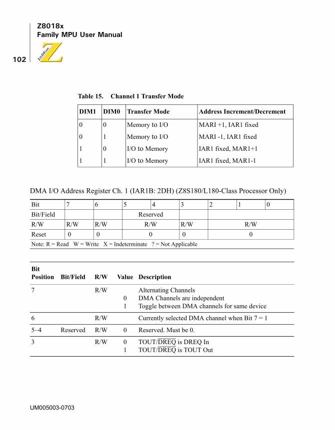
Z8018xFamily MPU User Manual
102
Table 15. Channel 1 Transfer Mode
DIM1 DIM0 Transfer Mode Address Increment/Decrement
0 0 Memory�to I/O MARI +1, IAR1 fixed
0 1 Memory�to I/O MARI -1, IAR1 fixed
1 0 I/O�to Memory IAR1 fixed, MAR1+1
1 1 I/O�to Memory IAR1 fixed, MAR1-1
DMA I/O Address Register Ch. 1 (IAR1B: 2DH) (Z8S180/L180-Class Processor Only)
Bit 7 6 5 4 3 2 1 0Bit/Field ReservedR/W R/W R/W R/W R/W R/WReset 0 0 0 0 0 Note: R = Read W = Write X = Indeterminate ? = Not Applicable
BitPosition Bit/Field R/W Value Description
7 R/W01
Alternating ChannelsDMA Channels are independentToggle between DMA channels for same device
6 R/W Currently selected DMA channel when Bit 7 = 1
5–4 Reserved R/W 0 Reserved. Must be 0.
3 R/W 01
TOUT/DREQ is DREQ InTOUT/DREQ is TOUT Out
UM005003-0703
Z8018xFamily MPU User Manual
103
DMA Register Description
Bit 7
This bit must be set to 1 only when both DMA channels are set to take their requests from the same device. If this bit is 1 (it resets to 0), the TEND output of DMA channel o sets a flip-flop, so that thereafter the device’s request is visible to channel 1, but not visible to channel 0. The internal TEND signal of channel 1 clears the FF, so that thereafter, the device’s request is visible to channel 0, but no visible to channel 1.
If DMA request are from differing sources, DMA channel 0 request is forced onto DMA channel 1 after TEND output of DMA channel 0 sets the flop-flop to alternate.
Bit 6
When both DMA channels are programmed to take their requests from the same device, this bit (FF mentioned in the previous paragraph) controls which channel the device’s request is presented to: 0 = DMA0, 1 = DMA l. When Bit 7 is 1, this bit is automatically toggled by the channel end output of the channels.
2-0 R/W 000001010011111
DMA1 ext TOUT/DREQDMA1 ASCI0DMA1 ASCI1DMA1 ESCCDMA1 PIA27-20 (P1284)
BitPosition Bit/Field R/W Value Description
UM005003-0703
Z8018xFamily MPU User Manual
104
Bits 5–3
Reserved. Must be 0.
Bits 2–0
With DIM1, bit 1 of DCNTL, these bits control which request is presented to DMA channel 1, as described below:
DMA Operation
This section discusses the three DMA operation modes for channel 0:
• Memory to/from memory
• Memory to/from I/O
• Memory to/from memory mapped I/O
DIM1 IAR18–16 Request Routed to DMA Channel 1
0000000
00000101001110X1X0111
DREQ1ASCI0 TxASCI1 Txext CKA0/DREQ0ReservedReservedReserved
1111111
00000101001110X1X0111
ext DREQ1ASCI0 RxASCI1 Rxext CKA0/DREQ0ReservedReservedReserved
UM005003-0703

Z8018xFamily MPU User Manual
105
In addition, the operation of channel 0 DMA with the on-chip ASCI (Asynchronous Serial Communication Interface) as well as Channel 1 DMA are described.
Memory to Memory—Channel 0
For memory to/from memory transfers, the external DREQ0 input is not used for DMA transfer timing. Rather, the DMA operation is timed in one of two programmable modes – BURST or CYCLE STEAL. In both modes, the DMA operation automatically proceeds until termination (shown by byte count-BCR0) = 0.
In BURST mode, the DMA operation proceeds until termination. In this case, the CPU cannot perform any program execution until the DMA operation is completed. In CYCLE STEAL mode, the DMA and CPU operation are alternated after each DMA byte transfer until the DMA is completed. The sequence:
• 1 CPU Machine Cycle
• DMA Byte Transfer
is repeated until DMA is completed. Figure 46 describes CYCLE STEAL mode DMA timing.
UM005003-0703
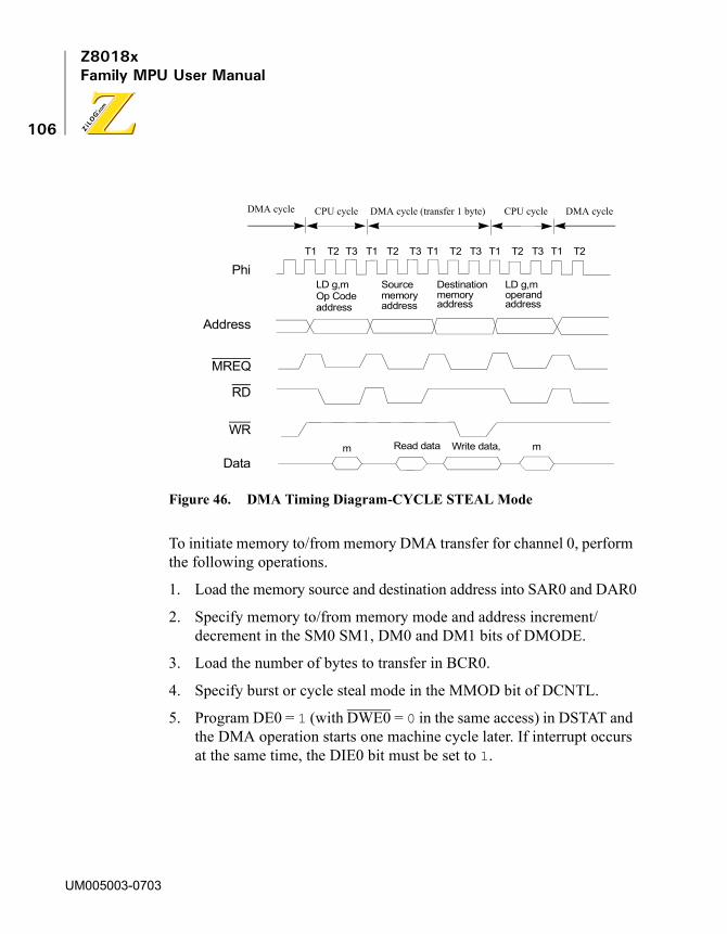
Z8018xFamily MPU User Manual
106
Figure 46. DMA Timing Diagram-CYCLE STEAL Mode
To initiate memory to/from memory DMA transfer for channel 0, perform the following operations.
1. Load the memory source and destination address into SAR0 and DAR0
2. Specify memory to/from memory mode and address increment/decrement in the SM0 SM1, DM0 and DM1 bits of DMODE.
3. Load the number of bytes to transfer in BCR0.
4. Specify burst or cycle steal mode in the MMOD bit of DCNTL.
5. Program DE0 = 1 (with DWE0 = 0 in the same access) in DSTAT and the DMA operation starts one machine cycle later. If interrupt occurs at the same time, the DIE0 bit must be set to 1.
T1 T2T1 T2T1 T2T1 T3 T3T3T2T3T1 T2
DMA cycle CPU cycle DMA cycle (transfer 1 byte) CPU cycle DMA cycle
LD g,mOp Code
Sourcememory
Destinationmemory
LD g,moperand
WR
MREQ
Address
Data
RD
m Read data
Phi
Write data, m
address address address address
UM005003-0703
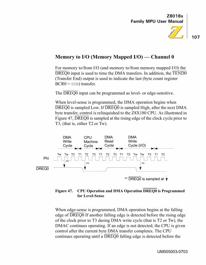
Z8018xFamily MPU User Manual
107
Memory to I/O (Memory Mapped I/O) — Channel 0
For memory to/from I/O (and memory to/from memory mapped I/O) the DREQ0 input is used to time the DMA transfers. In addition, the TEND0 (Transfer End) output is used to indicate the last (byte count register BCR0 = 00H) transfer.
The DREQ0 input can be programmed as level- or edge-sensitive.
When level-sense is programmed, the DMA operation begins when DREQ0 is sampled Low. If DREQ0 is sampled High, after the next DMA byte transfer, control is relinquished to the Z8X180 CPU. As illustrated in Figure 47, DREQ0 is sampled at the rising edge of the clock cycle prior to T3, (that is, either T2 or Tw).
Figure 47. CPU Operation and DMA Operation DREQ0 is Programmed for Level-Sense
When edge-sense is programmed, DMA operation begins at the falling edge of DREQ0 If another falling edge is detected before the rising edge of the clock prior to T3 during DMA write cycle (that is T2 or Tw), the DMAC continues operating. If an edge is not detected, the CPU is given control after the current byte DMA transfer completes. The CPU continues operating until a DREQ0 falling edge is detected before the
Tw T1 T2 T3Tw Tw TwT1 T1 T1T2 T2 T2T3 T3T3
DMA CPU DMA DMA
** ** **
** DREQ0 is sampled at
DREQ0
Phi
WriteCycle
MachineCycle
ReadCycle
WriteCycle (I/O)
UM005003-0703

Z8018xFamily MPU User Manual
108
rising edge of the clock prior to T3 at which time the DMA operation (re)starts. Figure 48 depicts the edge-sense DMA timing.
Figure 48. CPU Operation and DMA Operation DREQ0 is Programmed for Edge-Sense
During the transfers for channel 0, the TEND0 output goes Low synchronous with the write cycle of the last (BCR0 = OOH) DMA transfer (Reference Figure 49).
Figure 49. TEND0 Output Timing Diagram
The DREQ0 and TEND0 pins are programmably multiplexed with the CKA0 and CKA1 ASCI clock input/outputs. However, when DMA channel 0 is programmed for memory to/from I/O (and memory to/from
Tw T1 T2 T3 TwT1 T1 T1T2 T2 T2T3 T3T3
DMA CPU DMA
** **
** DREQ0 is sampled at
DREQ0
Phi
** **
T3
WriteCycle
MachineCycle
ReadCycle
DMAWriteCycle
CPUMachineCycle
TEND0
Phi
Last DMA cycle (BCR0 = 00H)
DMA read cycle DMA write cycle
T1 T2 T3 TW T3T2T1
UM005003-0703
Z8018xFamily MPU User Manual
109
memory mapped I/O. transfers, the CKA0/DREQ0 pin automatically functions as input pin or output pin even if it has been programmed as output pin for CKA0. And the CKA1/TEND0 pin functions as an input or an output pin for TEND0 by setting CKA1D to 1 in CNTLA1.
To initiate memory to/from I/O (and memory to/from memory mappedI/O) DMA transfer for channel 0, perform the following operations:
1. Load the memory and I/O or memory mapped I/O source and destination addresses into SAR0 and DAR0.
I/O addresses (not memory mapped I/O are limited to 16 bits (A0–A15). Make sure that bits A16, A17 and A19 are 0 (A18 is a don't care) to correctly enable the external DREQ0 input.
2. Specify memory to/from I/O or memory to/from memory mapped I/O mode and address increment/decrement in the SM0, SM1, DM0 and DM1 bits of DMODE.
3. Load the number of bytes to transfer in BCR0.
4. Specify whether DREQ0 is edge- or level-sense by programming the DMS0 bit of DCNTL.
5. Enable or disable DMA termination interrupt with the DIE0 bit in DSTAT.
6. Program DE0: = 1 (with DWEO = 0 in the same access) in DSTAT and the DMA operation begins under the control of the DREQ0 input.
Memory to ASCI - Channel 0
Channel 0 has extra capability to support DMA transfer to/from the on-chip two channel ASCI. In this case, the external DREQ0 input is not used for DMA timing. Rather, the ASCI status bits are used to generate an internal DREQ0 The TDRE (Transmit Data Register Empty) bit and the RDRF (Receive Data Register Full) bit are used to generate an internal
UM005003-0703

Z8018xFamily MPU User Manual
110
DREQ0 for ASCI transmission and reception respectively. To initiate memory to/from ASCI DMA transfer, perform the following operations:
1. Load the source and destination addresses into SAR0 and DAR0 Specify the I/O (ASCI) address as follows:
a. Bits A0–A7 must contain the address of the ASCI channel transmitter or receiver (I/O addresses 6H-9H).
b. Bits A8–A15 must equal 0.
c. Bits SAR17–SAR16 must be set according to Table 16 to enable use of the appropriate ASCI status bit as an internal DMA request.
Table 16. DMA Transfer Request
SAR18 SAR17 SAR16 DMA Transfer Request
X 0 0 DREQ0
X 0 1 RDRF (ASCI channel 0)
X 1 0 RDRF (ASCI channel 1)
X 1 1 Reserved
Note: X = Don’t care
DAR18 DAR17 DAR16 DMA Transfer Request
X 0 0 DREQ0
X 0 1 TDRE (ASCI channel O)
X 1 0 TDRE (ASCI channel 1)
X 1 1 Reserved
Note: X = Don’t care
UM005003-0703

Z8018xFamily MPU User Manual
111
2. Specify memory � I/O transfer mode and address increment/decrement in the SM0, SM1, DM0 and DM1 bits of DMODE.
3. Load the number of bytes to transfer in BCR0
4. The DMA request sense mode (DMS0 bit in DCNTL) must be specified as edge sense.
5. Enable or disable DMA termination interrupt with the DIE0 bit in DSTAT.
6. Program DE0 =1 (with DWE0 = 0 in the same access) in DSTAT and the DMA operation with the ASCI begins under control of the ASCI generated internal DMA request.
The ASCI receiver or transmitter using DMA is initialized to allow the first DMA transfer to begin.
The ASCI receiver must be empty as shown by RDRF = 0.
The ASCI transmitter must be full as shown by TDRE = 0. Thus, the first byte is written to the ASCI Transmit Data Register under program control. The remaining bytes are transferred using DMA.
Channel 1 DMA
DMAC Channel 1 performs memory to/from I/O transfers. Except for different registers and status/control bits, operation is exactly the same as described for channel 0 memory to/from I/O DMA.
To initiate a DMA channel 1 memory to/from I/O transfer, perform the following operations:
1. Load the memory address (20 bits) into MAR1.
2. Load the I/O address (16 bits) into IAR1.
3. Program the source/destination and address increment/decrement mode using the DIM1 and DIM0 bits in DCNTL.
UM005003-0703

Z8018xFamily MPU User Manual
112
4. Specify whether DREQ1 is level- or edge- sense in the DMS1 bit in DCNTL.
5. Enable or disable DMA termination interrupt with the DIE1 bit in DSTAT.
6. Program DE1 = 1 (with DWE1 = 0 in the same access) in DSTAT and the DMA operation with the external I/O device begins using the external DREQ1 input and TEND1 output.
DMA Bus Timing
When memory (and memory mapped I/O) is specified as a source or destination, MREQ goes Low during the memory access. When I/O is specified as a source or destination, IORQ goes Low during the I/O access.
When I/O (and memory mapped I/O) is specified as a source or destination, the DMA timing is controlled by the external DREQ input and the TEND output indicates DMA termination
External I/O devices may not overlap addresses with internal I/O and control registers, even using DMA.
For I/O accesses, one Wait State is automatically inserted. Additional Wait States can be inserted by programming the on-chip wait state generator or using the external WAIT input.
For memory mapped I/O accesses, this automatic I/O Wait State is not inserted.
For memory to memory transfers (channel 0 only), the external DREQ0 input is ignored. Automatic DMA timing is programmed as either BURST or CYCLE STEAL.
When a DMA memory address carry/borrow between bits A15 and A16 of the address bus occurs (crossing 64KB boundaries), the minimum bus
Note:
Note:
UM005003-0703
Z8018xFamily MPU User Manual
113
cycle is extended to 4 clocks by automatic insertion of one internal Ti state.
DMAC Channel Priority
For simultaneous DREQ0 and DREQ1 requests, channel 0 has priority over channel 1. When channel 0 is performing a memory to/from memory transfer, channel 1 cannot operate until the channel 0 operation has terminated. If channel 1 is operating, channel 0 cannot operate until channel 1 releases control of the bus.
DMAC and BUSREQ, BUSACK
The BUSREQ and BUSACK inputs allow another bus master to take control of the Z8X180 bus. BUSREQ and BUSACK take priority over the on-chip DMAC and suspends DMAC operation. The DMAC releases the bus to the external bus master at the breakpoint of the DMAC memory or I/O access. Since a single byte DMAC transfer requires a read and a write cycle, it is possible for the DMAC to be suspended after the DMAC read, but before the DMAC write. Hence, when the external master releases the Z8X180 bus (BUSREQ High), the on-chip DMAC correctly continues the suspended DMA operation.
UM005003-0703
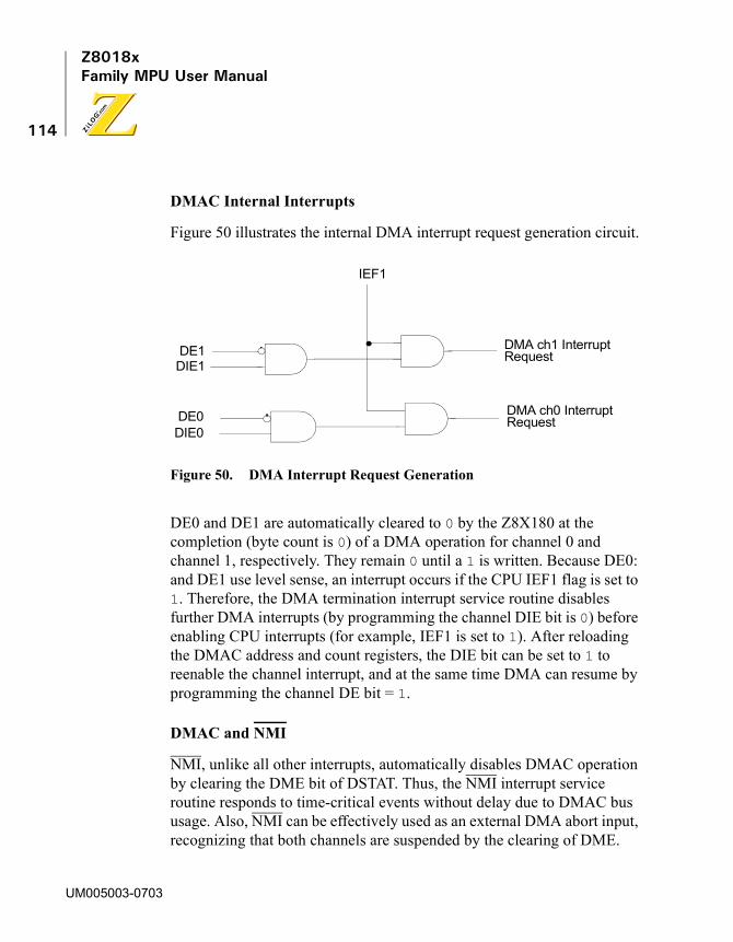
Z8018xFamily MPU User Manual
114
DMAC Internal Interrupts
Figure 50 illustrates the internal DMA interrupt request generation circuit.
Figure 50. DMA Interrupt Request Generation
DE0 and DE1 are automatically cleared to 0 by the Z8X180 at the completion (byte count is 0) of a DMA operation for channel 0 and channel 1, respectively. They remain 0 until a 1 is written. Because DE0: and DE1 use level sense, an interrupt occurs if the CPU IEF1 flag is set to 1. Therefore, the DMA termination interrupt service routine disables further DMA interrupts (by programming the channel DIE bit is 0) before enabling CPU interrupts (for example, IEF1 is set to 1). After reloading the DMAC address and count registers, the DIE bit can be set to 1 to reenable the channel interrupt, and at the same time DMA can resume by programming the channel DE bit = 1.
DMAC and NMI
NMI, unlike all other interrupts, automatically disables DMAC operation by clearing the DME bit of DSTAT. Thus, the NMI interrupt service routine responds to time-critical events without delay due to DMAC bus usage. Also, NMI can be effectively used as an external DMA abort input, recognizing that both channels are suspended by the clearing of DME.
DE1DIE1
DE0DIE0
IEF1
DMA ch1 InterruptRequest
DMA ch0 InterruptRequest
UM005003-0703
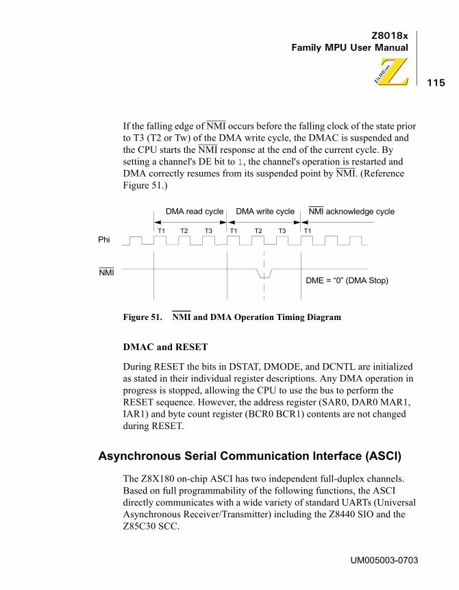
Z8018xFamily MPU User Manual
115
If the falling edge of NMI occurs before the falling clock of the state prior to T3 (T2 or Tw) of the DMA write cycle, the DMAC is suspended and the CPU starts the NMI response at the end of the current cycle. By setting a channel's DE bit to 1, the channel's operation is restarted and DMA correctly resumes from its suspended point by NMI. (Reference Figure 51.)
Figure 51. NMI and DMA Operation Timing Diagram
DMAC and RESET
During RESET the bits in DSTAT, DMODE, and DCNTL are initialized as stated in their individual register descriptions. Any DMA operation in progress is stopped, allowing the CPU to use the bus to perform the RESET sequence. However, the address register (SAR0, DAR0 MAR1, IAR1) and byte count register (BCR0 BCR1) contents are not changed during RESET.
Asynchronous Serial Communication Interface (ASCI)
The Z8X180 on-chip ASCI has two independent full-duplex channels. Based on full programmability of the following functions, the ASCI directly communicates with a wide variety of standard UARTs (Universal Asynchronous Receiver/Transmitter) including the Z8440 SIO and the Z85C30 SCC.
NMI
Phi
DMA write cycle
T1 T2 T3 T3T2T1
DMA read cycle NMI acknowledge cycle
DME = “0” (DMA Stop)
T1
UM005003-0703
Z8018xFamily MPU User Manual
116
The key functions for ASCI on Z80180, Z8S180 and Z8L180 class processors are listed below. Each channel is independently programmable.
• Full-duplex communication
• 7- or 8-bit data length
• Program controlled 9th data bit for multiprocessor communication
• 1 or 2 stop bits
• Odd, even, no parity
• Parity, overrun, framing error detection
• Programmable baud rate generator, /16 and /64 modes
• Modem control signals – Channel 0 contains DCD0, CTS0 and RTS0; Channel 1 contains CTS1
• Programmable interrupt condition enable and disable
• Operation with on-chip DMAC
ASCI Block Diagram for the Z8S180/Z8L180-Class Processors
Figure 52 illustrates the ASCI block diagram.
UM005003-0703
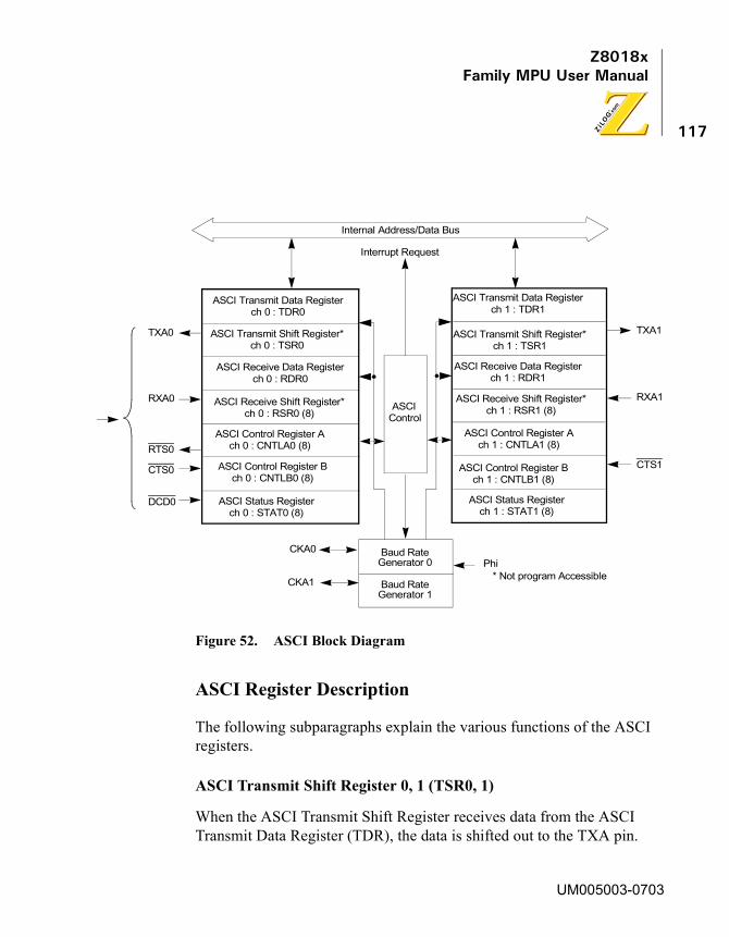
Z8018xFamily MPU User Manual
117
Figure 52. ASCI Block Diagram
ASCI Register Description
The following subparagraphs explain the various functions of the ASCI registers.
ASCI Transmit Shift Register 0, 1 (TSR0, 1)
When the ASCI Transmit Shift Register receives data from the ASCI Transmit Data Register (TDR), the data is shifted out to the TXA pin.
TXA1
Phi
Internal Address/Data Bus
Interrupt Request
ASCI Transmit Data Registerch 0 : TDR0
ASCI Transmit Shift Register*ch 0 : TSR0
ASCI Receive Data Registerch 0 : RDR0
ASCI Receive Shift Register*ch 0 : RSR0 (8)
ASCI Control Register Ach 0 : CNTLA0 (8)
ASCI Control Register Bch 0 : CNTLB0 (8)
ASCI Status Registerch 0 : STAT0 (8)
CKA1 * Not program Accessible
Baud RateGenerator 0
Baud RateGenerator 1
ASCI Status Registerch 1 : STAT1 (8)
ASCI Control Register Bch 1 : CNTLB1 (8)
ASCI Control Register Ach 1 : CNTLA1 (8)
ASCI Transmit Data Registerch 1 : TDR1
ASCI Transmit Shift Register*ch 1 : TSR1
ASCI Receive Data Registerch 1 : RDR1
ASCI Receive Shift Register*ch 1 : RSR1 (8)ASCI
Control
RXA1
CKA0
CTS1RTS0
CTS0
DCD0
TXA0
RXA0
UM005003-0703
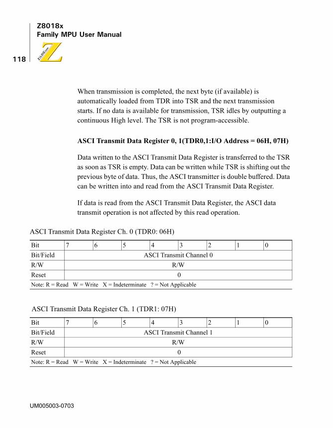
Z8018xFamily MPU User Manual
118
When transmission is completed, the next byte (if available) is automatically loaded from TDR into TSR and the next transmission starts. If no data is available for transmission, TSR idles by outputting a continuous High level. The TSR is not program-accessible.
ASCI Transmit Data Register 0, 1(TDR0,1:I/O Address = 06H, 07H)
Data written to the ASCI Transmit Data Register is transferred to the TSR as soon as TSR is empty. Data can be written while TSR is shifting out the previous byte of data. Thus, the ASCI transmitter is double buffered. Data can be written into and read from the ASCI Transmit Data Register.
If data is read from the ASCI Transmit Data Register, the ASCI data transmit operation is not affected by this read operation.
ASCI Transmit Data Register Ch. 0 (TDR0: 06H)
Bit 7 6 5 4 3 2 1 0Bit/Field ASCI Transmit Channel 0R/W R/WReset 0Note: R = Read W = Write X = Indeterminate ? = Not Applicable
ASCI Transmit Data Register Ch. 1 (TDR1: 07H)
Bit 7 6 5 4 3 2 1 0Bit/Field ASCI Transmit Channel 1R/W R/WReset 0Note: R = Read W = Write X = Indeterminate ? = Not Applicable
UM005003-0703

Z8018xFamily MPU User Manual
119
ASCI Receive Shift Register 0,1(RSR0, 1)
This register receives data shifted in on the RXA pin. When full, data is automatically transferred to the ASCI Receive Data Register (RDR) if it is empty. If RSR is not empty when the next incoming data byte is shifted in, an overrun error occurs. The RSR is not program-accessible.
ASCI Receive Data Register 0,1 (RDR0, 1: I/O Address = 08H, 09H)
When a complete incoming data byte is assembled in RSR, it is automatically transferred to the RDR if RDR is empty. The next incoming data byte can be shifted into RSR while RDR contains the previous received data byte. Thus, the ASCI receiver on Z80180 is double- buffered.
\
On the Z8S180 and Z8L180-class processors are quadruple buffered. The ASCI Receive Data Register is a read-only register. However, if RDRF =
ASCI Receive Data Register Ch. 0 (RDR0: 08H)
Bit 7 6 5 4 3 2 1 0Bit/Field ASCI Receive Channel 0R/W R/WReset 0Note: R = Read W = Write X = Indeterminate ? = Not Applicable
ASCI Receive Data Register Ch. 1 (RDR1: 09H)
Bit 7 6 5 4 3 2 1 0Bit/Field ASCI Receive Channel 1R/W R/WReset 0Note: R = Read W = Write X = Indeterminate ? = Not Applicable
UM005003-0703

Z8018xFamily MPU User Manual
120
0, data can be written into the ASCII Receive Data Register, and the data can be read.
ASCI Status Register 0, 1 (STAT0, 1)
Each channel status register allows interrogation of ASCI communication, error and modem control signal status, and enabling or disabling of ASCI interrupts.
ASCI Status Register 0 (STAT0: 04H)
Bit 7 6 5 4 3 2 1 0Bit/Field RDRF OVRN PE FE RIE DCD0 TDRE TIER/W R R R R R/W R R R/WReset 0 0 0 0 0 0 0 0 Note: R = Read W = Write X = Indeterminate ? = Not Applicable
BitPosition Bit/Field R/W Value Description
7 RDRF R Receive Data Register Full — RDRF is set to 1 when an incoming data byte is loaded into RDR. If a framing or parity error occurs, RDRF remains set and the receive data (which generated the error) is still loaded into RDR. RDRF is cleared to 0 by reading RDR, when the DCD0 input is High, in IOSTOP mode, and during RESET.
6 OVRN R Overrun Error — OVRN is set to 1 when RDR is full and RSR becomes full. OVRN is cleared to 0 when the EFR bit (Error Flag Reset) of CNTLA is written to 0, when DCD0 is High, in IOSTOP mode, and during RESET.
UM005003-0703
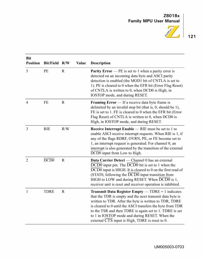
Z8018xFamily MPU User Manual
121
5 PE R Parity Error — PE is set to 1 when a parity error is detected on an incoming data byte and ASCI parity detection is enabled (the MOD1 bit of CNTLA is set to 1). PE is cleared to 0 when the EFR bit (Error Flag Reset) of CNTLA is written to 0, when DCD0 is High, in IOSTOP mode, and during RESET.
4 FE R Framing Error — If a receive data byte frame is delimited by an invalid stop bit (that is, 0, should be 1), FE is set to 1. FE is cleared to 0 when the EFR bit (Error Flag Reset) of CNTLA is written to 0, when DCD0 is High, in IOSTOP mode, and during RESET.
3 RIE R/W Receive Interrupt Enable — RIE must be set to 1 to enable ASCI receive interrupt requests. When RIE is 1, if any of the flags RDRF, OVRN, PE, or FE become set to 1, an interrupt request is generated. For channel 0, an interrupt is also generated by the transition of the external DCD0 input from Low to High.
2 DCD0 R Data Carrier Detect — Channel 0 has an external DCD0 input pin. The DCD0 bit is set to 1 when the DCD0 input is HIGH. It is cleared to 0 on the first read of (STAT0, following the DCD0 input transition from HIGH to LOW and during RESET. When DCD0 is 1, receiver unit is reset and receiver operation is inhibited.
1 TDRE R Transmit Data Register Empty — TDRE = 1 indicates that the TDR is empty and the next transmit data byte is written to TDR. After the byte is written to TDR, TDRE is cleared to 0 until the ASCI transfers the byte from TDR to the TSR and then TDRE is again set to 1. TDRE is set to 1 in IOSTOP mode and during RESET. When the external CTS input is High, TDRE is reset to 0.
BitPosition Bit/Field R/W Value Description
UM005003-0703
Z8018xFamily MPU User Manual
122
0 TIE R/W Transmit Interrupt Enable — TIE must be set to 1 to enable ASCI transmit interrupt requests. If TIE is 1, an interrupt is requested when TDRE is 1. TIE is cleared to 0 during RESET.
BitPosition Bit/Field R/W Value Description
UM005003-0703

Z8018xFamily MPU User Manual
123
ASCI Control Register A0, 1 (CNTLA0, 1)
Each ASCI channel Control Register A configures the major operating modes such as receiver/transmitter enable and disable, data format, and multiprocessor communication mode.
ASCI Status Register 1 (STAT1: 05H)
Bit 7 6 5 4 3 2 1 0Bit/Field RDRF OVRN PE FE RIE CTS1E TDRE TIER/W R R R R R/W R/W R R/WReset 0 0 0 0 0 0 0 0 Note: R = Read W = Write X = Indeterminate ? = Not Applicable
BitPosition Bit/Field R/W Value Description
7 RDRF R Receive Data Register Full — RDRF is set to 1 when an incoming data byte is loaded into RDR. Note that if a framing or parity error occurs, RDRF is still set and the receive data (which generated the error) is still loaded into RDR. RDRF is cleared to 0 by reading RDR, when the DCD0 input is High, in IOSTOP mode, and during RESET.
6 OVRN R Overrun Error — OVRN is set to 1 when RDR is full and RSR becomes full. OVRN is cleared to 0 when the EFR bit (Error Flag Reset) of CNTLA is written to 0, when DCD0 is High, in IOSTOP mode, and during RESET.
5 PE R Parity Error — PE is set to 1 when a parity error is detected on an incoming data byte and ASCI parity detection is enabled (the MOD1 bit of CNTLA is set to 1). PE is cleared to 0 when the EFR bit (Error Flag Reset) of CNTLA is written to 0, when DCD0 is High, in IOSTOP mode, and during RESET.
UM005003-0703

Z8018xFamily MPU User Manual
124
4 FE R Framing Error — If a receive data byte frame is delimited by an invalid stop bit (that is, 0, should be 1), FE is set to 1. FE is cleared to 0 when the EFR bit (Error Flag Reset) of CNTLA is written to 0, when DCD0 is High, in IOSTOP mode, and during RESET.
3 RIE R/W Receive Interrupt Enable — RIE must be set to 1 to enable ASCI receive interrupt requests. When RIE is 1, if any of the flags RDRF, OVRN, PE, or FE become set to 1, an interrupt request is generated. For channel 0, an interrupt is also generated by the transition of the external DCD0 input from Low to High.
2 CTS1E R/W Channel 1 CTS Enable — Channel 1 has an external CTS1 input which is multiplexed with the receive data pin (RXS) for the CSI/O (Clocked Serial I/O Port). Setting CTS1E to 1 selects the CTS1 function and clearing CTS1E to 0 selects the RXS function.
1 TDRE R Transmit Data Register Empty — TDRE = 1 indicates that the TDR is empty and the next transmit data byte is written to TDR. After the byte is written to TDR, TDRE is cleared to 0 until the ASCI transfers the byte from TDR to the TSR and then TDRE is again set to 1. TDRE is set to 1 in IOSTOP mode and during RESET. When the external CTS input is High, TDRE is reset to 0.
0 TIE R/W Transmit Interrupt Enable — TIE must be set to 1 to enable ASCI transmit interrupt requests. If TIE is 1, an interrupt is requested when TDRE is 1. TIE is cleared to 0 during RESET.
BitPosition Bit/Field R/W Value Description
UM005003-0703

Z8018xFamily MPU User Manual
125
ASCI Control Register A0, 1 (CNTLA0, 1)
Each ASCI channel Control Register A configures the major operating modes such as receiver/transmitter enable and disable, data format, and multiprocessor communication mode.
ASCI Control Register A 0 (CNTLA0: 00H)
Bit 7 6 5 4 3 2 1 0Bit/Field MPE RE TE RTS0 MPBR/
EFRMOD2 MOD1 MOD0
R/W R/W R/W R/W R/W R/W R/W R/W R/WReset 0 0 0 1 X 0 0 0 Note: R = Read W = Write X = Indeterminate ? = Not Applicable
BitPosition Bit/Field R/W Value Description
7 MPE R/W Multi-Processor Mode Enable — The ASCI has a multiprocessor communication mode which utilizes an extra data bit for selective communication when a number of processors share a common serial bus. Multiprocessor data format is selected when the MP bit in CNTLB is set to 1. If multiprocessor mode is not selected (MP bit in CNTLB = 0), MPE has no effect. If multiprocessor mode is selected, MPE enables or disables the wakeup feature as follows. If MPE is set to 1, only received bytes in which the MPB (multiprocessor bit) is 1 can affect the RDRF and error flags. Effectively, other bytes (with MPB is 0) are ignored by the ASCI. If MPE is reset to 0, all bytes, regardless of the state of the MPB data bit, affect the RDRF and error flags.
UM005003-0703
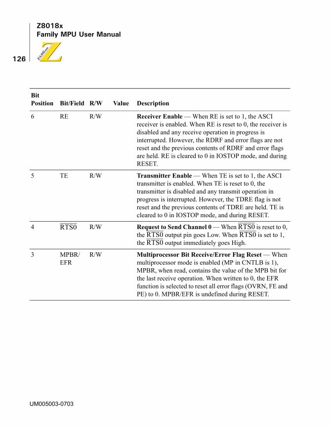
Z8018xFamily MPU User Manual
126
6 RE R/W Receiver Enable — When RE is set to 1, the ASCI receiver is enabled. When RE is reset to 0, the receiver is disabled and any receive operation in progress is interrupted. However, the RDRF and error flags are not reset and the previous contents of RDRF and error flags are held. RE is cleared to 0 in IOSTOP mode, and during RESET.
5 TE R/W Transmitter Enable — When TE is set to 1, the ASCI transmitter is enabled. When TE is reset to 0, the transmitter is disabled and any transmit operation in progress is interrupted. However, the TDRE flag is not reset and the previous contents of TDRE are held. TE is cleared to 0 in IOSTOP mode, and during RESET.
4 RTS0 R/W Request to Send Channel 0 — When RTS0 is reset to 0, the RTS0 output pin goes Low. When RTS0 is set to 1, the RTS0 output immediately goes High.
3 MPBR/EFR
R/W Multiprocessor Bit Receive/Error Flag Reset — When multiprocessor mode is enabled (MP in CNTLB is 1), MPBR, when read, contains the value of the MPB bit for the last receive operation. When written to 0, the EFR function is selected to reset all error flags (OVRN, FE and PE) to 0. MPBR/EFR is undefined during RESET.
BitPosition Bit/Field R/W Value Description
UM005003-0703

Z8018xFamily MPU User Manual
127
2–0 MOD2–0 R/W ASCI Data Format Mode 2, 1, 0 — These bits program the ASCI data format as follows.
MOD20: 7 bit data1: 8 bit data
MOD10: No parity1: Parity enabled
MOD00: 1 stop bit1: 2 stop bits
The data formats available based on all combinations of MOD2, MOD1 and MOD0 are described in Table 17.
BitPosition Bit/Field R/W Value Description
UM005003-0703

Z8018xFamily MPU User Manual
128
ASCI Control Register A 1 (CNTLA1: 01H)
Bit 7 6 5 4 3 2 1 0Bit/Field MPE RE TE CKA1D MPBR/
EFRMOD2 MOD1 MOD0
R/W R/W R/W R/W R/W R/W R/W R/W R/WReset 0 0 0 0 X 0 0 0 R = Read W = Write X = Indeterminate ? = Not Applicable
BitPosition Bit/Field R/W Value Description
7 MPE R/W Multi-Processor Mode Enable — The ASCI has a multiprocessor communication mode which utilizes an extra data bit for selective communication when a number of processors share a common serial bus. Multiprocessor data format is selected when the MP bit in CNTLB is set to 1. If multiprocessor mode is not selected (MP bit in CNTLB = 0), MPE has no effect. If multiprocessor mode is selected, MPE enables or disables the wakeup feature as follows. If MPE is set to 1, only received bytes in which the MPB (multiprocessor bit) is 1 can affect the RDRF and error flags. Effectively, other bytes (with MPB = 0) are ignored by the ASCI. If MPE is reset to 0, all bytes, regardless of the state of the MPB data bit, affect the RDRF and error flags.
6 RE R/W Receiver Enable — When RE is set to 1, the ASCI receiver is enabled. When RE is reset to 0, the receiver is disabled and any receive operation in progress is interrupted. However, the RDRF and error flags are not reset and the previous contents of RDRF and error flags are held. RE is cleared to 0 in IOSTOP mode, and during RESET.
UM005003-0703
Z8018xFamily MPU User Manual
129
5 TE R/W Transmitter Enable — When TE is set to 1, the ASCI transmitter is enabled. When TE is reset to 0, the transmitter is disabled and any transmit operation in progress is interrupted. However, the TDRE flag is not reset and the previous contents of TDRE are held. TE is cleared to 0 in IOSTOP mode, and during RESET.
4 CKA1D R/W CKA1 Clock Disable — When CKA1D is set to 1, the multiplexed CKA1/TEND0 pin is used for the TEND0 function. When CKA1 D is 0, the pin is used as CKA1, an external data dock input/output for channel 1
3 MPBR/EFR
R/W Multiprocessor Bit Receive/Error Flag Reset — When multiprocessor mode is enabled (MP in CNTLB is 1), MPBR, when read, contains the value of the MPB bit for the last receive operation. When written to 0, the EFR function is selected to reset all error flags (OVRN, FE and PE) to 0. MPBR/EFR is undefined during RESET.
BitPosition Bit/Field R/W Value Description
UM005003-0703
Z8018xFamily MPU User Manual
130
2–0 MOD2–0 R/W ASCI Data Format Mode 2, 1, 0 — These bits program the ASCI data format as follows.
MOD20: 7 bit data1: 8 bit data
MOD10: No parity1: Parity enabled
MOD00: 1 stop bit1: 2 stop bits
The data formats available based on all combinations of MOD2, MOD1 and MOD0 are described in Table 17.
BitPosition Bit/Field R/W Value Description
UM005003-0703

Z8018xFamily MPU User Manual
131
ASCI Control Register B0, 1 (CNTLB0, 1)
Each ASCI channel control register B configures multiprocessor mode, parity and baud rate selection.
Table 17. Data Formats
MOD2 MOD1 MOD0 Data Format
0 0 0 Start + 7 bit data + 1 stop
0 0 1 Start + 7 bit date + 2 Stop
0 1 0 Start + 7 bit data + parity + 1 stop
0 1 1 Start + 7 bit data + parity + 2 stop
1 0 0 Start + 8 bit data + 1 stop
1 0 1 Start + 8 bit data + 2 stop
1 1 0 Start + 8 bit data + parity + 1 stop
1 1 1 Start + 8 bit date + parity + 2 stop
UM005003-0703
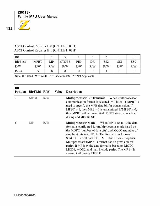
Z8018xFamily MPU User Manual
132
ASCI Control Register B 0 (CNTLB0: 02H)ASCI Control Register B 1 (CNTLB1: 03H)
Bit 7 6 5 4 3 2 1 0Bit/Field MPBT MP CTS/PS PE0 DR SS2 SS1 SS0R/W R/W R/W R/W R/W R/W R/W R/W R/WReset X 0 0 0 0 1 1 1Note: R = Read W = Write X = Indeterminate ? = Not Applicable
BitPosition Bit/Field R/W Value Description
7 MPBT R/W Multiprocessor Bit Transmit — When multiprocessor communication format is selected (MP bit is 1), MPBT is used to specify the MPB data bit for transmission. If MPBT is 1, then MPB = 1 is transmitted. If MPBT is 0, then MPBT = 0 is transmitted. MPBT state is undefined during and after RESET.
6 MP R/W Multiprocessor Mode — When MP is set to 1, the data format is configured for multiprocessor mode based on the MOD2 (number of data bits) and MOD0 (number of stop bits) bits in CNTLA. The format is as follows.Start bit + 7 or 8 data bits + MPB bit + 1 or 2 stop bitsMultiprocessor (MP = 1) format has no provision for parity. If MP is 0, the data format is based on MOD0 MOD1, MOD2, and may include parity. The MP bit is cleared to 0 during RESET.
UM005003-0703
Z8018xFamily MPU User Manual
133
The external ASCI channel 0 data clock pins are multiplexed with DMA control lines (CKA0/DREQ and CKA1/TEND0). During RESET, these
5 CTS/PS R/W Clear to Send/Prescale — When read, CTS/PS reflects the state of the external CTS input. If the CTS input pin is High, CTS/PS is read as 1. When the CTS input pin is High, the TDRE bit is inhibited (that is, held at 0). For channel 1, the CTS1 input is multiplexed with RXS pin (Clocked Serial Receive Data). Thus, CTS/PS is only valid when read if the channel 1 CTS1E bit is 1 and the CST1 input pin function is selected. The read data of CTS/PS is not affected by RESET.When written, CT /PS specifies the baud rate generator prescale factor. If CTS/PS is set to 1, the system clock is prescaled by 30 while if CTS/PS is cleared to 0, the system clock is prescaled by 10.CTS/PS is cleared to 0 during RESET.
4 PEO R/W Parity Even Odd — PE0 selects even or odd parity. PE0 does not affect the enabling/disabling of parity (MOD1 bit of CNTLA). If PE0 is cleared to 0, even parity is selected. If PE0 is set to 1, odd parity is selected.PE0 is cleared to 0 during RESET.
3 DR R/W Divide Ratio — DR specifies the divider used to obtain baud rate from the data sampling clock If DR is reset to 0, divide by 16 is used, while if DR is set to 1, divide by 64 is used. DR is cleared to 0 during RESET.
2–0 SS2–0 R/W Source/Speed Select — Specifies the data clock source (internal or external) and baud rate prescale factor. SS2, SS1, and SS0 are all set to 1 during RESET. Table 18 describes the divide ratio corresponding to SS2, SS1 and SS0
BitPosition Bit/Field R/W Value Description
UM005003-0703

Z8018xFamily MPU User Manual
134
pins are initialized as ASCI data clock inputs. If SS2, SS1 and SS0 are reprogrammed (any other value than SS2, SS1, SS0 = 1) these pins become ASCI data clock inputs. However, if DMAC channel 0 is configured to perform memory to/from I/O (and memory mapped I/O) transfers the CKA0/DREQ0 pin reverts to DMA control signals regardless of SS2, SS1, SS0 programming.
Also, if the CKA1D bit in the CNTLA register is 1, then the CKA1/TEND0 reverts to the DMA Control output function regardless of SS2, SS1 and SS0 programming. Final data clock rates are based on CTS/PS (prescale), DR, SS2, SS1, SS0 and the Z8X180 system clock frequency (Reference Table 19).
Each ASCI channel control register B configures multiprocessor mode, parity and baud rate selection.
Table 18. Divide Ratio
SS2 SS1 SS0 Divide Ratio
0 0 0 � 1
0 0 1 � 2
0 1 0 � 4
0 1 1 � 8
1 0 0 � 16
1 0 1 � 32
1 1 0 � 64
1 1 1 external clock
UM005003-0703
Z8018xFamily MPU User Manual
135
ASCI0 Extension Control Register (I/O Address: 12H) (Z8S180/L180-Class Processors Only)
Bit 7 6 5 4 3 2 1 0Bit/Field RDRF
Int Inhibit
DCD0Disable
CTS0 Disable
X1 Bit Clk
ASCI0
BRG0 Mode
Break Feature Enable
Break Detect (RO)
Send Break
R/W R/W R/W R/W R/W R/W R/W R/W R/WReset 0 0 0 0 0 0 0 0Note: R = Read W = Write X = Indeterminate ? = Not Applicable
BitPosition Bit/Field R/W Value Description
7 RDRF Interrupt Inhibit
R/W 01
RDRF Interrupt Inhibit OnRDRF Interrupt Inhibit Off
6 DCD0 Disable
R/W 01
DCD0 Auto-enables RxDCD0 advisory to SW
5 CTS0 Disable
R/W 01
CTS0 Auto-enable TxCTS0 advisory to SW
4 X1 Bit Clk ASCI0
R/W 01
CKA0 /16 or /64CKA0 is bit clock
3 BRG0 Mode
R/W 01
As S180Enable 16-bit BRG counter
2 Break Feature Enable
R/W 01
Break Feature Enable OnBreak Feature Enable Off
1 Break Detect (RO)
R/W 01
Break Detect OnBreak Detect Off
UM005003-0703

Z8018xFamily MPU User Manual
136
Each ASCI channel control register B configures multiprocessor mode, parity and baud rate selection.
0 Send Break
R/W 01
Normal XmitDrive TXA Low
ASCI1 Extension Control Register (I/O Address: 13H) (Z8S180/L180-Class Processors Only)
Bit 7 6 5 4 3 2 1 0Bit/Field RDRF
Int Inhibit
Reserved X1 Bit Clk
ASCI1
BRG1 Mode
Break Feature Enable
Break Detect (RO)
Send Break
R/W R/W ? R/W R/W R/W R/W R/WReset 0 0 0 0 0 0 0Note: R = Read W = Write X = Indeterminate ? = Not Applicable
BitPosition Bit/Field R/W Value Description
7 RDRF Interrupt Inhibit
R/W 01
RDRF Interrupt Inhibit OnRDRF Interrupt Inhibit Off
6–5 Reserved ? 0 Reserved. Must be 0
4 X1 Bit Clk ASCI1
R/W 01
CKA1 /16 or /64CKA1 is bit clock
3 BRG1 Mode
R/W 01
As S180Enable 16-bit BRG counter
BitPosition Bit/Field R/W Value Description
UM005003-0703
Z8018xFamily MPU User Manual
137
Each ASCI channel control register B configures multiprocessor mode, parity and baud rate selection.
2 Break Feature Enable
R/W 01
Break Feature Enable OnBreak Feature Enable Off
1 Break Detect (RO)
R/W 01
Break Detect OnBreak Detect Off
0 Send Break
R/W 01
Normal XmitDrive TXA Low
ASCI0 Time Constant Low Register (I/O Address: 1AH) (Z8S180/L180-Class Processors Only)
Bit 7 6 5 4 3 2 1 0R/W R/W R/W R/W R/W R/W R/W R/W R/WReset 0 0 0 0 0 0 0 0Note: R = Read W = Write X = Indeterminate ? = Not Applicable
ASCI0 Time Constant High Register (I/O Address: 1BH) (Z8S180/L180-Class Processors Only)
Bit 7 6 5 4 3 2 1 0R/W R/W R/W R/W R/W R/W R/W R/W R/WReset 0 0 0 0 0 0 0 0Note: R = Read W = Write X = Indeterminate ? = Not Applicable
BitPosition Bit/Field R/W Value Description
UM005003-0703
Z8018xFamily MPU User Manual
138
Modem Control Signals
ASCI channel 0 has CTS0, DCD0 and RTS0 external modem control signals. ASCI channel 1 has a CTS1 modem control signal which is multiplexed with Clocked Serial Receive Data (RXS).
CTS0: Clear to Send 0 (Input)
The CTS0 input allows external control (start/stop) of ASCI channel 0 transmit operations. When CTS0 is High, the channel 0 TDRE bit is held at 0 whether or not the TDR0 (Transmit Data Register) is full or empty. When CTS0 is Low, TDRE reflects the state of TDR0. The actual transmit operation is not disabled by CT High, only TDRE is inhibited:
DCD0: Data Carrier Detect 0 (Input)
The DCD0 input allows external control (start/stop) of ASCI channel 0 receive operations. When DCD0 is High, the channel 0 RDRF bit is held at 0 whether or not the RDR0, (Receive Data Register) is full or empty.
ASCI1 Time Constant Low Register (I/O Address: 1CH) (Z8S180/L180-Class Processors Only)
Bit 7 6 5 4 3 2 1 0R/W R/W R/W R/W R/W R/W R/W R/W R/WReset 0 0 0 0 0 0 0 0Note: R = Read W = Write X = Indeterminate ? = Not Applicable
ASCI1 Time Constant High Register (I/O Address: 1DH) (Z8S180/L180-Class Processors Only)
Bit 7 6 5 4 3 2 1 0R/W R/W R/W R/W R/W R/W R/W R/W R/WReset 0 0 0 0 0 0 0 0Note: R = Read W = Write X = Indeterminate ? = Not Applicable
UM005003-0703

Z8018xFamily MPU User Manual
139
The error flags (PE, FE, and OVRN bits) are also held at 0. Even after the DCD0 input goes Low, these bits do not resume normal operation until the status register (STAT0, is read. This first read of (STAT0, while enabling normal operation, still indicates the DCD0 input is High (DCD0 bit = 1) even though it has gone Low. Thus, the STAT0 register must be read twice to ensure the DCD0 bit is reset to 0:
RTS0: Request to Send 0 (Output)
RTS0 allows the ASCI to control (start/stop) another communication devices transmission (for example, by connection to that device's CTS input). RTS0 is essentially a 1-bit output port, having no side effects on other ASCI registers or flags.
CTS1: Clear to Send 1 (Input)
Channel 1 CTS1 input is multiplexed with Clocked Serial Receive Data (RXS). The CTS1 function is selected when the CTS1E bit in STAT1 is set to 1. When enabled, the CTS1 operation is equivalent to CTS0,
Modem control signal timing is depicted in Figure 53 and Figure 54.
Figure 53. DCD0 Timing Diagram
DCD0 Pin
DCD0 Flag
Status Register Read
UM005003-0703
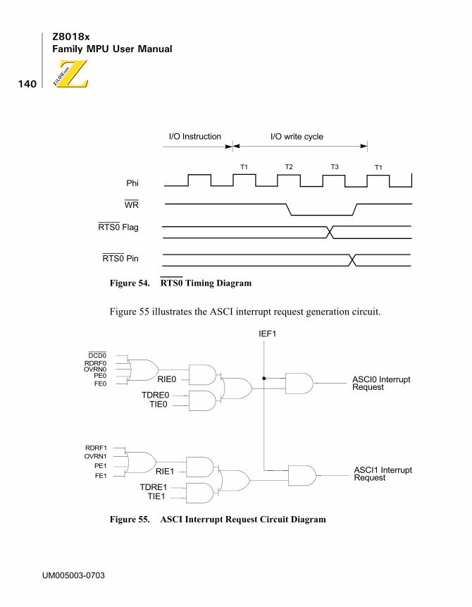
Z8018xFamily MPU User Manual
140
Figure 54. RTS0 Timing Diagram
Figure 55 illustrates the ASCI interrupt request generation circuit.
Figure 55. ASCI Interrupt Request Circuit Diagram
T1 T1T2 T3
WR
RTS0 Flag
RTS0 Pin
Phi
I/O Instruction I/O write cycle
IEF1
ASCI0 InterruptRequest
ASCI1 InterruptRequest
TIE1TDRE1
RIE1
RDRF1OVRN1
PE1FE1
TIE0TDRE0
RIE0
DCD0
OVRN0PE0FE0
RDRF0
UM005003-0703

Z8018xFamily MPU User Manual
141
ASCI to/from DMAC Operation
Operation of the ASCI with the on-chip DMAC channel 0 requires that the DMAC be correctly configured to use the ASCI flags as DMA request signals.
ASCI and RESET
During RESET, the ASCI status and control registers are initialized as defined in the individual register descriptions.
Receive and Transmit operations are stopped during RESET. However, the contents of the transmit and receive data registers (TDR and RDR) are not changed by RESET.
ASCI Clock
When in external clock input mode, the external clock is directly input to the sampling rate (�16/�64) as depicted in Figure 56.
Figure 56. ASCI Clock
External Clockfc � Phi � 40
Internal ClockPhi
Baud Rate Selection Prescaler Sampling Rate�1 to �64 �10 ��30 �16 �64
UM005003-0703
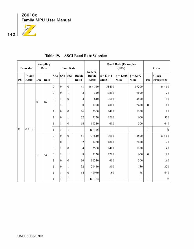
Z8018xFamily MPU User Manual
142
Table 19. ASCI Baud Rate Selection
PrescalerSampling
Rate Baud RateGeneralDivideRatio
Baud Rate (Example)(BPS) CKA
PSDivideRatio DR Rate
SS2 SS1 SS0 DivideRatio
� = 6.144MHz
� = 4.608MHz
� = 3.072MHz I/O
ClockFrequency
0 � � 10
0 16
0 0 0 �1 � � 160 38400 19200 � � 10
0 0 1 2 320 19200 9600 20
0 1 0 4 640 9600 4800 40
0 1 1 8 1280 4800 2400 0 80
1 0 0 16 2560 2400 1200 160
1 0 1 32 5120 1200 600 320
1 1 0 64 10240 600 300 640
1 1 1 — fc � 16 — — — I fc
1 64
0 0 0 �1 0�640 9600 4800 � � 10
0 0 1 2 1280 4800 2400 20
0 1 0 4 2560 2400 1200 40
0 1 1 8 5120 1200 600 0 80
1 0 0 16 10240 600 300 160
1 0 1 32 20480 300 150 320
1 1 0 64 40960 150 75 640
1 1 1 — fc � 64 — — — I fc
UM005003-0703

Z8018xFamily MPU User Manual
143
Baud Rate Generator(Z8S180/Z8L180-Class Processors Only)
The Z8S180/Z8L180 Baud Rate Generator (BRG) features two modes. The first is the same as in the Z80180. The second is a 16-bit down counter that divides the processor clock by the value in a 16-bit time constant register, and is identical to the DMSCC BRG. This feature allows
1 � � 30
0 16
0 0 0 �1 � � 480 9600 � � 30
0 0 1 2 960 4800 60
0 1 0 4 1920 2400 120
0 1 1 8 3840 1200 0 240
1 0 0 16 7680 600 480
1 0 1 32 15360 300 960
1 1 0 64 30720 150 1920
1 1 1 — fc � 16 — — — I fc
1 64
0 0 0 �1 � � 1920 2400 � � 30
0 0 1 2 3840 1200 60
0 1 0 4 7680 600 120
0 1 1 8 15360 300 0 240
1 0 0 16 30720 150 480
1 0 1 32 61440 75 960
1 1 0 64 122880 37.5 1920
1 1 1 — fc � 64 — — — I fc
Table 19. ASCI Baud Rate Selection (Continued)
PrescalerSampling
Rate Baud RateGeneralDivideRatio
Baud Rate (Example)(BPS) CKA
PSDivideRatio DR Rate
SS2 SS1 SS0 DivideRatio
� = 6.144MHz
� = 4.608MHz
� = 3.072MHz I/O
ClockFrequency
UM005003-0703

Z8018xFamily MPU User Manual
144
a common baud rate of up to 512 Kbps to be selected. The BRG can also be disabled in favor of an external clock on the CKA pin.
The Receiver and Transmitter subsequently divide the output of the BRG (or the signal from the CKA pin) by 1, 16, or 64, under the control of the DR bit in the CNTLB register, and the X1 bit in the ASCI Extension Control REgister. To compute baud rate, use the following formulas:
Where:
BRG mode is bit 3 of the ASEXT register
PS is bit 5 of the CNTLB register
TC is the 16-bit value in the ASCI Time Constant register
If ss2.1.0 = 111, baud rate - fCKA/Clock mode
else if BRG mode baud rate = fPHI/(2*(TC+2)*Clock mode)
else baud rate -fPHI/((10 + 20*PS) * 2^ss*Clock mode)
The TC value for a given baud rate is:
TC = (fPHI/*2*baud rate*Clock mode)) -2
Clock mode depends on bit 4 in ASEXT and bit 3 in CNTLB, as described in Table 20.
Table 20.Clock Mode Bit Values
X1 DR Clock Mode
0011
0101
16641Reserved, do not use
UM005003-0703
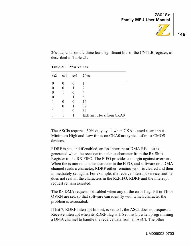
Z8018xFamily MPU User Manual
145
2^ss depends on the three least significant bits of the CNTLB register, as described in Table 21.
The ASCIs require a 50% duty cycle when CKA is used as an input. Minimum High and Low times on CKA0 are typical of most CMOS devices.
RDRF is set, and if enabled, an Rx Interrupt or DMA REquest is generated when the receiver transfers a character from the Rx Shift Register to the RX FIFO. The FIFO provides a margin against overruns. When the is more than one character in the FIFO, and software or a DMA channel reads a character, RDRF either remains set or is cleared and then immediately set again. For example, if a receive interrupt service routine does not real all the characters in the RxFIFO, RDRF and the interrupt request remain asserted.
The Rx DMA request is disabled when any of the error flags PE or FE or OVRN are set, so that software can identify with which character the problem is associated.
If Bit 7, RDRF Interrupt Inhibit, is set to 1, the ASCI does not request a Receive interrupt when its RDRF flag is 1. Set this bit when programming a DMA channel to handle the receive data from an ASCI. The other
Table 21. 2^ss Values
ss2 ss1 ss0 2^ss
00001111
00110011
01010101
1248163264External Clock from CKA0
UM005003-0703

Z8018xFamily MPU User Manual
146
causes for an ASCI Receive interrupt (PE, FE, OVRN, and for ASCI0, DCD) continue to request RX interrupt if the RIE bit is 1. The Rx DMA request is inhibited if PE or FE or OVRN is set, so that software can detect where an error occurred. When the RIE bit is 0, as it is after a Reset, RDRF causes an ASCI interrupt if RIE is 1.
Clocked Serial I/O Port (CSI/O)The Z8X180 includes a simple, high-speed clock, synchronous serial I/O port. The CSI/O includes transmit/receive (half-duplex), fixed 8-bit data, and internal or external data clock selection. High-speed operation (baud rate 200Kbps at fC = 4 MHz) is provided. The CSI/O is ideal for implementing a multiprocessor communication link between multiple Z8X180s. These secondary devices may typically perform a portion of the system I/O processing, (that is, keyboard scan/decode, LDC interface, for instance).
CSI/O Block Diagram
The CSI/O block diagram is illustrated in Figure 57. The CSI/O consists of two registers–the Transmit/Receive Data Register (TRDR) and Control Register (CNTR).
UM005003-0703

Z8018xFamily MPU User Manual
147
Figure 57. CSI/O Block Diagram
CSI/O Registers Description
CSI/O Control/Status Register (CNTR: I/O Address 0AH)
CNTR is used to monitor CSI/O status, enable and disable the CSI/O, enable and disable interrupt generation, and select the data clock speed and source.
CSI/O Control/Status Register (CNTR: 0AH)
Bit 7 6 5 4 3 2 1 0Bit/Field EF EIE RE TE — SS2 SS1 SS0R/W R R/W R/W R/W R/W R/W R/WReset 0 0 0 0 1 1 1Note: R = Read W = Write X = Indeterminate ? = Not Applicable
Phi
Internal Address/Data Bus
TXS
RXS
Interrupt Request
Baud RateGenerator
CKSCSI/O Transmit/ReceiveData Register:TRDR (8)
CSI/O Control Register:CNTR (8)
UM005003-0703
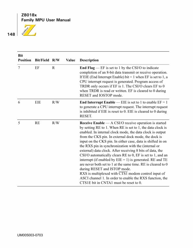
Z8018xFamily MPU User Manual
148
BitPosition Bit/Field R/W Value Description
7 EF R End Flag — EF is set to 1 by the CSI/O to indicate completion of an 8-bit data transmit or receive operation. If EIE (End Interrupt Enable) bit = 1 when EF is set to 1, a CPU interrupt request is generated. Program access of TRDR only occurs if EF is 1. The CSI/O clears EF to 0 when TRDR is read or written. EF is cleared to 0 during RESET and IOSTOP mode.
6 EIE R/W End Interrupt Enable — EIE is set to 1 to enable EF = 1 to generate a CPU interrupt request. The interrupt request is inhibited if EIE is reset to 0. EIE is cleared to 0 during RESET.
5 RE R/W Receive Enable — A CSI/O receive operation is started by setting RE to 1. When RE is set to 1, the data clock is enabled. In internal clock mode, the data clock is output from the CKS pin. In external dock mode, the dock is input on the CKS pin. In either case, data is shifted in on the RXS pin in synchronization with the (internal or external) data clock. After receiving 8 bits of data, the CSI/O automatically clears RE to 0, EF is set to 1, and an interrupt (if enabled by EIE = 1) is generated. RE and TE are never both set to 1 at the same time. RE is cleared to 0 during RESET and ISTOP mode.RXS is multiplexed with CTS1 modem control input of ASCI channel 1. In order to enable the RXS function, the CTS1E bit in CNTA1 must be reset to 0.
UM005003-0703

Z8018xFamily MPU User Manual
149
CSI/O Transmit/Receive Data Register (TRDR: I/O Address = 0BH).
TRDR is used for both CSI/O transmission and reception. Thus, the system design must insure that the constraints of half-duplex operation are met (Transmit and receive operation cannot occur simultaneously). For example, if a CSI/O transmission is attempted while the CSI/O is receiving data, the CSI/O does not work.
TRDR is not buffered. Attempting to perform a CSI/O transmit while the previous transmit data is still being shifted out causes the shift data to be immediately updated, thereby corrupting the transmit operation in progress. Similarly, reading TRDR during a transmit or receive must be avoided.
4 TE R/W Transmit Enable — A CSI/O transmit operation is started by setting TE to 1. When TE is set to 1, the data clock is enabled. When in internal clock mode, the data clock is output from the CKS pin. In external clock mode, the clock is input on the CKS pin. In either case, data is shifted out on the TXS pin synchronous with the (internal or external) data clock. After transmitting 8 bits of data, the CSI/O automatically clears TE to 0, EF is set to 1, and an interrupt (if enabled by EIE = 1) is generated. TE and RE are never both set to 1 at the same time. TE is cleared to 0 during RESET and IOSTOP mode.
2–0 SS2–0 R/W Speed Select — Selects the CSI/O transmit/receive clock source and speed. SS2, SS I and SS0 are all set to 1 during RESET. Table 22 shows CSI/O Baud Rate Selection.
BitPosition Bit/Field R/W Value Description
UM005003-0703

Z8018xFamily MPU User Manual
150
After RESET, the CKS pin is configured as an external clock input (SS2, SS1, SS0 = 1). Changing these values causes CKS to become an output pin and the selected clock is output when transmit or receive operations are enabled.
CSI/O Interrupts
The CSI/O interrupt request circuit is shown in Figure 58.
CSI/O Transmit/Receive Register (TRDR: 0BH)
Bit 7 6 5 4 3 2 1 0Bit/Field CSI/O Transmit/Receive DataR/W R/WReset 0Note: R = Read W = Write X = Indeterminate ? = Not Applicable
Table 22. CSI/O Baud Rate Selection
SS2 SS1 SS0 Divide Ratio Baud Rate
0 0 0 � 20 (200000)
0 0 1 � 40 (100000)
0 1 0 � 80 (50000)
0 1 1 � 160 (25000)
1 0 0 � 320 (12500)
1 0 1 � 640 (6250)
1 1 0 � 1280 (3125)
1 1 1 External Clock input (less than � 20)
Note: ( ) indicates the baud rate (BPS) at Phi = 4 MHz.
UM005003-0703
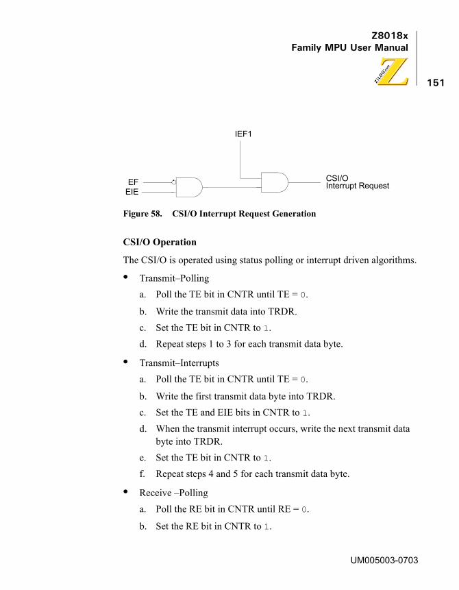
Z8018xFamily MPU User Manual
151
Figure 58. CSI/O Interrupt Request Generation
CSI/O Operation
The CSI/O is operated using status polling or interrupt driven algorithms.
• Transmit–Pollinga. Poll the TE bit in CNTR until TE = 0.
b. Write the transmit data into TRDR.c. Set the TE bit in CNTR to 1.d. Repeat steps 1 to 3 for each transmit data byte.
• Transmit–Interruptsa. Poll the TE bit in CNTR until TE = 0.
b. Write the first transmit data byte into TRDR.c. Set the TE and EIE bits in CNTR to 1.d. When the transmit interrupt occurs, write the next transmit data
byte into TRDR.e. Set the TE bit in CNTR to 1.f. Repeat steps 4 and 5 for each transmit data byte.
• Receive –Pollinga. Poll the RE bit in CNTR until RE = 0.
b. Set the RE bit in CNTR to 1.
EFEIE
IEF1
CSI/O Interrupt Request
UM005003-0703

Z8018xFamily MPU User Manual
152
c. Poll the RE bit in CNTR until RE = 0.
d. Read the receive data from TRDR.
e. Repeat steps 2 to 4 for each receive data byte.
• Receive–Interrupts
a. Poll the RE bit in CNTR until RE is 0.
b. Set the RE and EIE bits in CNTR to 1.
c. When the receive interrupt occurs read the receive data from TRDR.
d. Set the RE bit in CNTR to 1.
e. Repeat steps 3 and 4 for each receive data byte.
CSI/O Operation Timing Notes
• Transmitter clocking and receiver sampling timings are different from internal and external clocking modes. Figure 59 to Figure 62 illustrate CSI/O Transmit/Receive Timing.
• The transmitter and receiver is disabled TE and RE = 0) when initializing or changing the baud rate.
CSI/O Operation Notes
• Disable the transmitter and receiver (TE and RE = 0) before initializing or changing the baud rate. When changing the baud rate after completion of transmission or reception, a delay of at least one bit time is required before baud rate modification.
• When RE or TE is cleared to 0 by software, a corresponding receive or transmit operation is immediately terminated. Normally, TE or RE is only cleared to 0 when EF is 1.
• Simultaneous transmission and reception is not possible. Thus, TE and RE are not both 1 at the same time.
UM005003-0703

Z8018xFamily MPU User Manual
153
CSI/O and RESET
During RESET each bit in the CNTR is initialized as defined in the CNTR register description. CSI/O transmit and receive operations in progress are aborted during RESET. However, the contents of TRDR are not changed.
Figure 59. Transmit Timing Diagram–Internal Clock
CKS
TXS
TE
EF
LSB MSB
Read or write of CSI/OTransmit/Receive
Data Register
UM005003-0703

Z8018xFamily MPU User Manual
154
Figure 60. Transmit Timing–External Clock
CKS
TXS
TE
EF
Read or write of CSI/OTransmit/ReceiveData Register
2.5� 2.5� 2.5� 2.5�7.5� 7.5� 7.5� 7.5�
LSB MSB
UM005003-0703

Z8018xFamily MPU User Manual
155
Figure 61. CSI/O Receive Timing–Internal Clock
CKS
RXS
RE
EF
Read or write of CSI/OTransmit/Receive
Data Register
11� 11� 11� 11�
Sampling
17�
LSB MSB
UM005003-0703

Z8018xFamily MPU User Manual
156
Figure 62. CSI/O Receive Timing–External Clock
Programmable Reload Timer (PRT)The Z8X180 contains a two channel 16-bit Programmable Reload Timer. Each PRT channel contains a 16-bit down counter and a 16-bit reload register. The down counter is directly read and written and a down counter overflow interrupt can be programmably enabled or disabled. Also, PRT channel 1 features a TOUT output pin (multiplexed with A18) which can be set High, Low, or toggled. Thus, PRT1 can perform programmable output waveform generation.
PRT Block Diagram
The PRT block diagram is depicted in Figure 63. The two channels feature separate timer data and reload registers and a common status/
CKS
RXS
RE
EF
Read or write of CSI/OTransmit/Receive
Data Register
11.5�
Sampling
LSB MSB
11.5� 11.5� 11.5�
16.5� 16.5� 16.5� 16.5�
UM005003-0703

Z8018xFamily MPU User Manual
157
control register. The PRT input clock for both channels is equal to the system clock divided by 20.
Figure 63. PRT Block Diagram
PRT Register Description
Timer Data Register (TMDR: I/O Address - CH0: 0CH, 0DH; CH1: 15H, 14H). PRT0 and PRT1 each contain 16-bit timer Data Registers (TMDR). TMDR0 and TMDR1 are each accessed as low and high byte registers (TMDR0H, TMDR0L and TMDR1H, TMDR1L). During RESET, TMDR0 and TMDR1 are set to FFFFH.
TMDR is decremented once every twenty clocks. When TMDR counts down to 0, it is automatically reloaded with the value contained in the Reload Register (RLDR).
TMDR is read and written by software using the following procedures. The read procedure uses a PRT internal temporary storage register to
Phi � 20
Internal Address/Data Bus
TOUT
Timer DataRegister 0L: TMDR0L (8)
Timer DataRegister 0H: TMDR0H (8)
Timer ReloadRegister 0L: RLDR0L (8)
Timer ReloadRegister 0H: RLDR0H (8)
Timer ControlRegister: TCR (8)
Phi � 20
Timer DataRegister 1L: TMDR1L (8)
Timer DataRegister 1H: TMDR1H (8)
Timer ReloadRegister 1L: RLDR1L (8)
Timer ReloadRegister 1H: RLDR1H (8)
Interrupt Register
UM005003-0703
Z8018xFamily MPU User Manual
158
return accurate data without requiring the timer to be stopped. The write procedure requires the PRT to be stopped.
For reading (without stopping the timer), TMDR is read in the order of lower byte - higher byte (TMDRnL, TMDRnH). The lower byte read (TMDRnL) stores the higher byte value in an internal register. The following higher byte read (TMDRnH) accesses this internal register. This procedure insures timer data validity by eliminating the problem of potential 16-bit timer updating between each 8-bit read. Specifically, reading TMDR in higher byte–lower byte order may result in invalid data. Note the implications of TMDR higher byte internal storage for applications which may read only the lower and/or higher bytes. In normal operation all TMDR read routines must access both the lower and higher bytes, in that order. For writing, the TMDR down counting must be inhibited using the TDE (Timer Down Count Enable) bits in the TCR (Timer Control Register). Then, any or both higher and lower bytes of TMDR can be freely written (and read) in any order.
CSI/O Transmit/Receive Data Register (TRDR: I/O Address = 0BH).
TRDR is used for both CSI/O transmission and reception. Thus, the system design must insure that the constraints of half-duplex operation are met (Transmit and receive operation cannot occur simultaneously). For example, if a CSI/O transmission is attempted while the CSI/O is receiving data, the CSI/O does not work.
TRDR is not buffered. Attempting to perform a CSI/O transmit while the previous transmit data is still being shifted out causes the shift data to be immediately updated, thereby corrupting the transmit operation in progress. Similarly, reading TRDR during a transmit or receive must be avoided.
UM005003-0703

Z8018xFamily MPU User Manual
159
Timer Reload Register (RLDR: I/O Address = CH0: 0EH, 0FH, CHI, 16H, 17H)
PRT0 and PRT1 each contain 16-bit Timer Reload Registers (RLDR). RLDR0 and RLDR1 are each accessed as low and high byte registers (RLDR0H, RLDR0L and RLDR1H, RLDR1L). During RESET, RLDR0 and RLDR1 are set to FFFFH
When the TMDR counts down to 0, it is automatically reloaded with the contents of RLDR.
Timer Data Register 0L (TMDR0L: 0CH)
Bit 7 6 5 4 3 2 1 0Bit/Field Timer DataR/W R/WReset 0Note: R = Read W = Write X = Indeterminate ? = Not Applicable
Timer Data Register 0H (TMDR0H: 0DH)
Bit 7 6 5 4 3 2 1 0Bit/Field Timer DataR/W R/WReset 0Note: R = Read W = Write X = Indeterminate ? = Not Applicable
UM005003-0703

Z8018xFamily MPU User Manual
160
Timer Reload Register Channel 0L (RLDR0L: 0EH)
Bit 7 6 5 4 3 2 1 0Bit/Field Timer Reload DataR/W R/WReset 0Note: R = Read W = Write X = Indeterminate ? = Not Applicable
Timer Reload Register Channel 0H (RLDR0L: 0FH)
Bit 7 6 5 4 3 2 1 0Bit/Field Timer Reload DataR/W R/WReset 0Note: R = Read W = Write X = Indeterminate ? = Not Applicable
Timer Data Register 1L (TMDR1L: 14H)
Bit 7 6 5 4 3 2 1 0Bit/Field Timer DataR/W R/WReset 0Note: R = Read W = Write X = Indeterminate ? = Not Applicable
Timer Data Register 1H (TMDR1H: 15H)
Bit 7 6 5 4 3 2 1 0Bit/Field Timer DataR/W R/WReset 0Note: R = Read W = Write X = Indeterminate ? = Not Applicable
UM005003-0703

Z8018xFamily MPU User Manual
161
Timer Control Register (TCR)
TCR monitors both channels (PRT0, PRT1) TMDR status. It also controls enabling and disabling of down counting and interrupts along with controlling output pin A18/TOUT for PRT1.
Timer Reload Register Channel 1L (RLDR1L: 16H)
Bit 7 6 5 4 3 2 1 0Bit/Field Timer Reload DataR/W R/WReset 0Note: R = Read W = Write X = Indeterminate ? = Not Applicable
Timer Reload Register Channel 1H (RLDR1H: 17H)
Bit 7 6 5 4 3 2 1 0Bit/Field Timer Reload DataR/W R/WReset 0Note: R = Read W = Write X = Indeterminate ? = Not Applicable
Timer Control Register (TCR: 10H)
Bit 7 6 5 4 3 2 1 0Bit/Field TIF1 TIF0 TIE1 TIE0 TOC1 TOC0 TDE1 TDE0R/W R R R/W R/W R/W R/W R/W R/WReset 0 0 0 0 0 0 0 0Note: R = Read W = Write X = Indeterminate ? = Not Applicable
UM005003-0703

Z8018xFamily MPU User Manual
162
BitPosition Bit/Field R/W Value Description
7–6 TIF1–0 R TIF1: Timer Interrupt Flag — When TMDR1 decrements to 0, TIF1 is set to 1. This generates an interrupt request if enabled by TIE1 = 1. TIF1 is reset to 0 when TCR is read and the higher or lower byte of TMDR1 is read. During RESET, TIF1 is cleared to 0.When TMDR0 decrements to 0, TIF0 is set to 1. This generates an interrupt request if enabled by TIE0 = 1. TIF0 is reset to 0 when TCR is read and the higher or lower byte of TMDR0 is read. During RESET, TIF0 is cleared to 0.
5–4 TIE1–0 R/W Timer Interrupt Enable — When TIE1 is set to 1, TIF1 = 1 generates a CPU interrupt request. When TIE1 is reset to 0, the interrupt request is inhibited. During RESET, TIE1 is cleared to 0.When TIE0 is set to 1, TIF0 = 1 generates a CPU interrupt request. When TIE0 is reset to 0, the interrupt request is inhibited. During RESET, TIE0 is cleared to 0.
3–2 TOC1–0 R/W Timer Output Control — TOC1, and TOC0 control the output of PRT1 using the multiplexed A18/TOUT pin as shown in Table 23. During RESET, TOC1 and TOC0 are cleared to 0. This selects the address function for A18/TOUT. By programming TOC1 and TOC0 the A18/TOUT pin can be forced HIGH, LOW, or toggled when TMDR1 decrements to 0. Reference Table 23.
1–0 TDE1–0 R/W Timer Down Count Enable — TDE1 and TDE0 enable and disable down counting for TMDR1 and TMDR0 respectively. When TDEn (n = 0, 1) is set to 1, down counting is executed for TMDRn. When TDEn is reset to 0, down counting is stopped and TMDRn is freely read or written. TDE1 and TDE0 are cleared to 0 during RESET and TMDRn does not decrement until TDEn is set to 1.
UM005003-0703
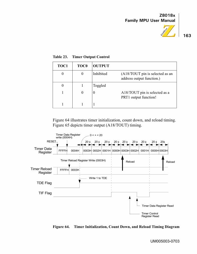
Z8018xFamily MPU User Manual
163
Figure 64 illustrates timer initialization, count down, and reload timing. Figure 65 depicts timer output (A18/TOUT) timing.
Figure 64. Timer Initialization, Count Down, and Reload Timing Diagram
Table 23. Timer Output Control
TOC1 TOC0 OUTPUT
0 0 Inhibited (A18/TOUT pin is selected as an address output function.)
0 1 Toggled
1 0 0 A18/TOUT pin is selected as a PRT1 output function!
1 1 1
Timer Data Registerwrite (0004H)
Timer DataRegister
RESET
ReloadReload
20 � 20 � 20 � 20 � 20 � 20 � 20�� 20 � 20�
0 < + < 20
FFFFH 0003H 0002H 0001H 0000H 0003H 0002H 0001H 0000H 0003H0004H
Timer Reload Register Write (0003H)
Timer Reload
TDE Flag
TIF Flag
Timer Data Register Read
Timer ControlRegister Read
Write 1 to TDE
FFFFH 0003HRegister
UM005003-0703

Z8018xFamily MPU User Manual
164
Figure 65. Timer Output Timing Diagram
PRT Interrupts
The PRT interrupt request circuit is illustrated in Figure 66.
Figure 66. PRT Interrupt Request Generation
PRT and RESET
During RESET, the bits in TCR are initialized as defined in the TCR register description. Down counting is stopped and the TMDR and RLDR registers are initialized to FFFFH. The A18/TOUT pin reverts to the address output function.
TOUT
Phi
Timer DataReg. = 0001H
Timer DataReg. = 0000H
TIF1TIE1
TIF0TIE0
IEF1
PRT1 InterruptRequest
PRT0 InterruptRequest
UM005003-0703
Z8018xFamily MPU User Manual
165
PRT Operation Notes
• TMDR data is accurately read without stopping down counting by reading the lower (TMDRnL*) and higher (TMDRnH*) bytes in that order. Also, TMDR is read or written by stopping the down counting.1
Take care to ensure that a timer reload does not occur during or between lower (RLDRnL*) and higher (RLDRnH*) byte writes. This may be guaranteed by system design/timing or by stopping down counting (with TMDR containing a non-zero value) during the RLDR updating. Similarly, in applications where TMDR is written at each TMDR overflow, the system/software design must guarantee that RLDR can be updated before the next overflow occurs. Otherwise, time base inaccuracy occurs.
• During RESET, the multiplexed A18/TOUT pin reverts to the address output. By reprogramming the TOC1 and TOC0 bits, the timer output function for PRT channel 1 is selected. The following paragraph describes the initial state of the TOUT pin after TOC1 and TOC0 are programmed to select the PRT channel 1 timer output function.
PRT (channel 1) has not counted down to 0.
If the PRT has not counted down to 0 (timed out), the initial state of TOUT depends on the programmed value in TOC1 and TOC0.
Secondary Bus Interface
E clock Output Timing
The Z8X180 also has a secondary bus interface that allows it to easily interface with other peripheral families.
1. *n = 0, 1
UM005003-0703
Z8018xFamily MPU User Manual
166
These devices require connection with the Z8X180 synchronous E clock output. The speed (access time) required for the peripheral devices are determined by the Z8X180 clock rate. Table 24, and Figure 67 through Figure 70 define E clock output timing.
Wait States are inserted in Op Code fetch, memory read/write, and I/O read/write cycles which extend the duration of E clock output High. During I/O read/write cycles with no Wait States (only occurs during on-chip I/O register accesses), E does not go High.
Table 24. E Clock Timing in Each Condition
Condition Duration of E Clock Output High
Op Code Fetch CycleMemory Read/Write Cycle
T2 rise - T3 fall (1.5 Phi + nw x Phi)
I/O read Cycle 1st Tw rise - T3 fall (0.5Phi + nw x Phi)
I/O Write Cycle 1st Tw rise - T3 rise Inw x Phi)
NMI Acknowledge 1st MC T2 rise - T3 fall (1.5 Phi)
INT0 Acknowledge 1st MC 1st Tw rise - T3 fall (0.50 + nw x Phi�
BUS RELEASE modeSLEEP modeSYSTEM STOP mode
Phi�fall - Phi�fall (2 Phi or 1 Phi)
Note: nw = the number of Wait States; MC: Machine Cycle
UM005003-0703
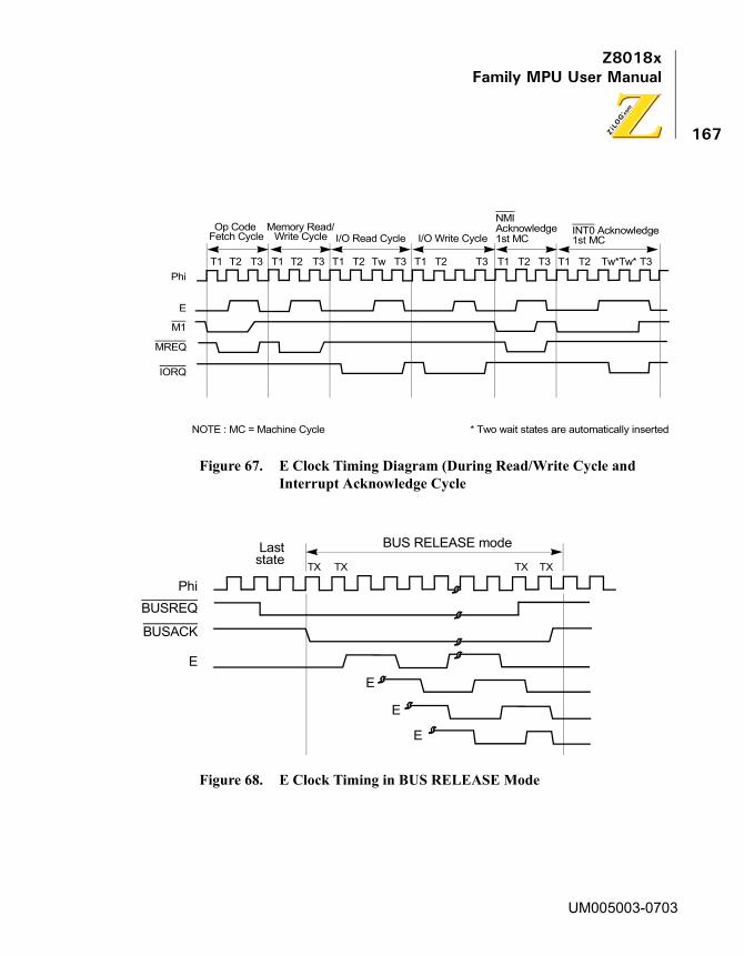
Z8018xFamily MPU User Manual
167
Figure 67. E Clock Timing Diagram (During Read/Write Cycle and Interrupt Acknowledge Cycle
Figure 68. E Clock Timing in BUS RELEASE Mode
Op Code Fetch Cycle
M1
MREQ
Phi
IORQ
Memory Read/Write Cycle I/O Write Cycle
NMIAcknowledge1st MC
INT0 Acknowledge1st MCI/O Read Cycle
NOTE : MC = Machine Cycle * Two wait states are automatically inserted
E
T1 T2 T3 Tw*T1T1 T1 T1 T1T2 T2 T2 T2 T2T3 T3 T3 T3 T3Tw Tw*
PhiBUSREQ
BUSACK
E
Laststate TX TX TX TX
BUS RELEASE mode
E
E
E
UM005003-0703
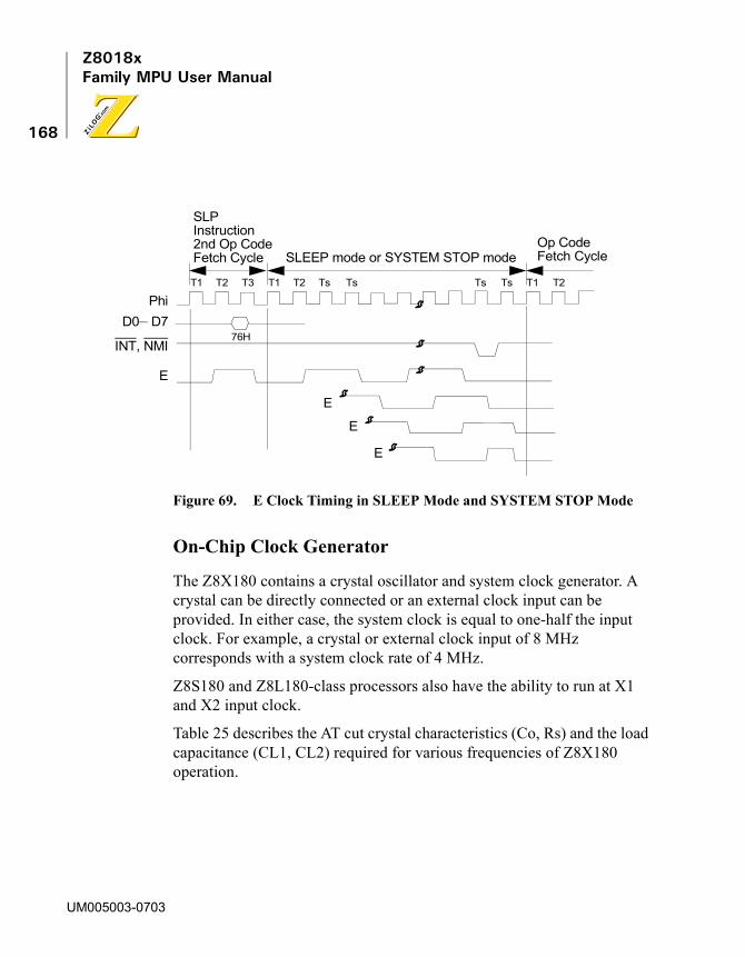
Z8018xFamily MPU User Manual
168
Figure 69. E Clock Timing in SLEEP Mode and SYSTEM STOP Mode
On-Chip Clock Generator
The Z8X180 contains a crystal oscillator and system clock generator. A crystal can be directly connected or an external clock input can be provided. In either case, the system clock is equal to one-half the input clock. For example, a crystal or external clock input of 8 MHz corresponds with a system clock rate of 4 MHz.
Z8S180 and Z8L180-class processors also have the ability to run at X1 and X2 input clock.
Table 25 describes the AT cut crystal characteristics (Co, Rs) and the load capacitance (CL1, CL2) required for various frequencies of Z8X180 operation.
E
E
E
T1 T2 T3 TsT1 T1T2 T2Ts Ts Ts
76H
SLPInstruction2nd Op CodeFetch Cycle SLEEP mode or SYSTEM STOP mode
Op CodeFetch Cycle
E
PhiD0– D7
INT, NMI
UM005003-0703
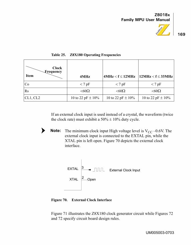
Z8018xFamily MPU User Manual
169
If an external clock input is used instead of a crystal, the waveform (twice the clock rate) must exhibit a 50% � 10% duty cycle.
The minimum clock input High voltage level is VCC –0.6V. The external clock input is connected to the EXTAL pin, while the XTAL pin is left open. Figure 70 depicts the external clock interface.
Figure 70. External Clock Interface
Figure 71 illustrates the Z8X180 clock generator circuit while Figures 72 and 72 specify circuit board design rules.
Table 25. Z8X180 Operating Frequencies
4MHz 4MHz � f 12MHz 12MHz � f 33MHz
Co � 7 pF � 7 pF � 7 pF
Rs �60 �60 �60
CL1, CL2 10 to 22 pF � 10% 10 to 22 pF � 10% 10 to 22 pF � 10%
Clock
ItemFrequency
Note:
EXTAL
XTAL
3
2 Open
External Clock Input
UM005003-0703
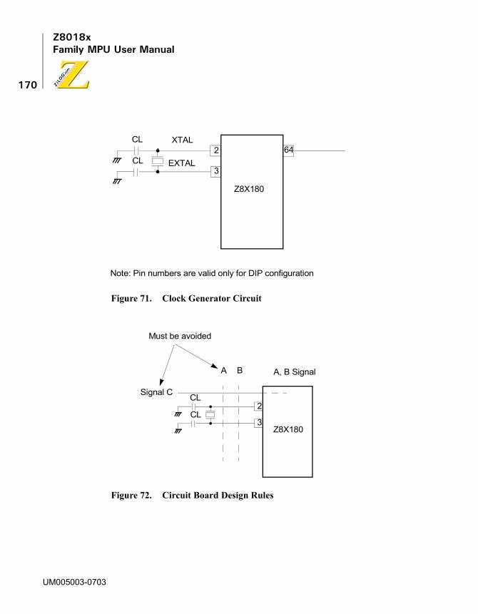
Z8018xFamily MPU User Manual
170
Figure 71. Clock Generator Circuit
Figure 72. Circuit Board Design Rules
Z8X180
XTAL
EXTAL2
3
64CL
CL
Note: Pin numbers are valid only for DIP configuration
Z8X180
2
3
CL
CL
Signal C
A, B SignalA B
Must be avoided
UM005003-0703

Z8018xFamily MPU User Manual
171
Figure 73. Example of Board Design
Circuit Board design should observe the following parameters.
• Locate the crystal and load capacitors as close to the IC as physically possible to reduce noise.
• Signal lines must not run parallel to the clock oscillator inputs. In particular, the clock input circuitry and the system clock output (pin 64) must be separated as much as possible.
• VCC power lines must be separated from the clock oscillator input circuitry.
• Resistivity between XTAL or EXTAL and the other pins must be greater than 10M ohms.
Signal line layout must avoid areas marked with the shaded area of Figure 73.
Signal line layout mustavoid shaded areas
20 mm max
20 m
m m
ax
Crystal
CL CL
6423
1
GND
Z8X180
Phi
Top View
Note: Pin mumbers valid only for DIP configuration
UM005003-0703

Z8018xFamily MPU User Manual
172
Miscellaneous
Free Running Counter (I/O Address = 18H)
If data is written into the free running counter, the interval of DRAM refresh cycle and baud rates for the ASCI and CSI/O are not guaranteed.
In IOSTOP mode, the free running counter continues counting down. It is initialized to FFH during RESET.
Free Running counter (FRC: 18H)
Bit 7 6 5 4 3 2 1 0Bit/Field Counting DataR/W RReset ?Note: R = Read W = Write X = Indeterminate ? = Not Applicable
UM005003-0703
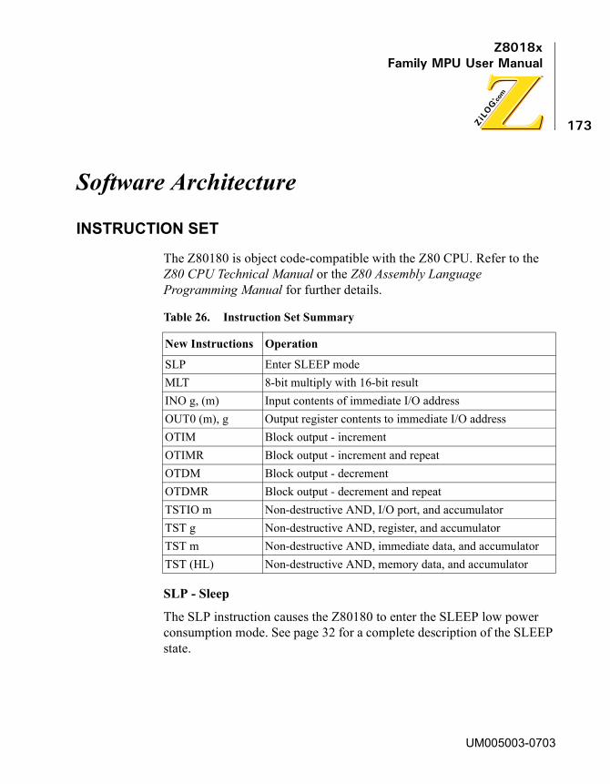
Z8018xFamily MPU User Manual
173
Software Architecture
INSTRUCTION SET
The Z80180 is object code-compatible with the Z80 CPU. Refer to the Z80 CPU Technical Manual or the Z80 Assembly Language Programming Manual for further details.
SLP - Sleep
The SLP instruction causes the Z80180 to enter the SLEEP low power consumption mode. See page 32 for a complete description of the SLEEP state.
Table 26. Instruction Set Summary
New Instructions Operation
SLP Enter SLEEP modeMLT 8-bit multiply with 16-bit resultINO g, (m) Input contents of immediate I/O addressOUT0 (m), g Output register contents to immediate I/O addressOTIM Block output - incrementOTIMR Block output - increment and repeatOTDM Block output - decrementOTDMR Block output - decrement and repeatTSTIO m Non-destructive AND, I/O port, and accumulatorTST g Non-destructive AND, register, and accumulatorTST m Non-destructive AND, immediate data, and accumulatorTST (HL) Non-destructive AND, memory data, and accumulator
UM005003-0703

Z8018xFamily MPU User Manual
174
MLT- Multiply
The MLT performs unsigned multiplication on two 8-bit numbers yielding a 16-bit result. MLT may specify BC, DE, HL, or SP registers. The 8-bit operands are loaded into each half of the 16-bit register and the 16-bit result is returned in that register.
OTIM, OTIMR, OTDM, OTDMR - Block I/O
The contents of memory pointed to by HL is output to the I/O address in (C). The memory address (HL) and I/O address (C) are incremented in OTIM and OTIMR and decremented in OTDM and OTDMR, respectively. The B register is decremented. The OTIMR and OTDMR variants repeat the above sequence until register B is decremented to 0. Since the I/O address (C) is automatically incremented or decremented, these instructions are useful for block I/O (such as Z80180 on-chip I/O) initialization. When I/O is accessed, 00H is output in high-order bits of address automatically.
TSTIO m - Test I/O Port
The contents of the I/O port addressed by C are ANDed with immediately specified 8-bit data and the status flags are updated. The I/O port contents are not written (non-destructive AND). When I/O is accessed, 00H is output in higher bits of address automatically.
TST g - Test Register
Perform an AND instruction on the contents of the specified register with the accumulator (A) and the status flags are updated. The accumulator and specified register are not changed (non-destructive AND).
TST m - Test Immediate
Perform an AND instruction on the contents of the immediately specified 8-bit data with the accumulator (A) and the status flags are updated. The accumulator is not changed (non-destructive AND).
UM005003-0703
Z8018xFamily MPU User Manual
175
TST (HL) - Test Memory
The contents of memory pointed to by HL are ANDed with the accumulator (A) and the status flags are updated. The memory contents and accumulator are not changed (non-destructive AND).
INO g, (m) - Input, Immediate I/O address
The contents of immediately specified 8-bit I/O address are input into the specified register. When I/O is accessed, 00H is output in high-order bits of the address automatically.
OUTO (m), g - Output, Immediate I/O address
The contents of the specified register are output to the immediately specified 8-bit I/O address. When I/O is accessed, 00H is output in high-order bits of the address automatically.
CPU REGISTERS
The Z80180 CPU registers consist of Register Set GR, Register Set GR' and Special Registers.
The Register Set GR consists of 8-bit Accumulator (A), 8-bit Flag Register (F), and three General Purpose Registers (BC, DE, and HL) which may be treated as 16-bit registers (BC, DE, and HL) or as individual 8-bit registers (B, C, D, E, H, and L) depending on the instruction to be executed. The Register Set GR' is alternate register set of Register Set GR and also contains Accumulator (A'), Flag Register (F') and three General Purpose Registers (BC', DE', and HL'). While the alternate Register Set GR' contents are not directly accessible, the contents can be programmably exchanged at high speed with those of Register Set GR.
The Special Registers consist of 8-bit Interrupt Vector Register (I), 8-bit R Counter (R), two 16-bit Index Registers (IX and IY), 16-bit Stack Pointer (SP), and 16-bit Program Counter (PC)
UM005003-0703

Z8018xFamily MPU User Manual
176
Figure 74 depicts CPU register configurations.
Figure 74. CPU Register Configurations
Accumulator (A, A')
The Accumulator (A) is the primary register used for many arithmetic, logical, and I/O instructions.
Flag Register F
B Register
D Register
H Register
C Register
E Register
L Register
General
Special RegisterInterrupt R Counter
I RIndex Register IX
Index Register IY
Stack Pointer SP
Program Counter PC
Register Set GR
Accumulator A
PurposeRegisters
Flag Register F'
B' Register
D' Register
H' Register
C' Register
E' Register
L' Register
General
Register Set GR'
Accumulator A'
PurposeRegisters
Vector Register
UM005003-0703

Z8018xFamily MPU User Manual
177
Flag Registers (F, F')
The flag registers store status bits (described in the next section) resulting from executed instructions.
General Purpose Registers (BC, BC', DE, DE', HL, HL')
The General Purpose Registers are used for both address and data operation. Depending on the instruction, each half (8 bits) of these registers (B, C, D, E, H, and I) may also be used.
Interrupt Vector Register (I)
For interrupts that require a vector table address to be calculated (INT0 Mode 2, INT1, INT2, and internal interrupts), the Interrupt Vector Register (I) provides the most significant byte of the vector table address. I is cleared to 00H during reset.
R Counter (R)
The least significant seven bits of the R counter (R) count the number of instructions executed by the Z80180. R increments for each CPU Op Code fetch cycle (each M1 cycle). R is cleared to 00H during reset.
Index Registers (IX, and IY)
The Index Registers are used for both address and data operations. For addressing, the contents of a displacement specified in the instruction are added to or subtracted from the Index Register to determine an effective operand address.
UM005003-0703

Z8018xFamily MPU User Manual
178
Stack Pointer (SP)
The Stack Pointer (SP) contains the memory address based LIFO stack. SP is cleared to 0000H during reset.
Program Counter (PC)
The Program Counter (PC) contains the address of the instruction to be executed and is automatically updated after each instruction fetch. PC is cleared to 0000H during reset.
Flag Register (F)
The Flag Register stores the logical state reflecting the results of instruction execution. The contents of the Flag Register are used to control program flow and instruction operation.
Flag Register
Bit 7 6 5 4 3 2 1 0Bit/Field S Z Not Used H Not Used P/V N CR/W R/W R/W ? R/W ? R/W R/W R/WReset 0 0 ? 0 ? 0 0 0R = Read W = Write X = Indeterminate ? = Not Applicable
BitPosition Bit/Field R/W Value Description
7 S R/W 0 Sign. S stores the state of the most significant bit (bit 7) of the result. This is useful for operations with signed numbers in which values with bit 7 = 1 are interpreted as negative.
UM005003-0703
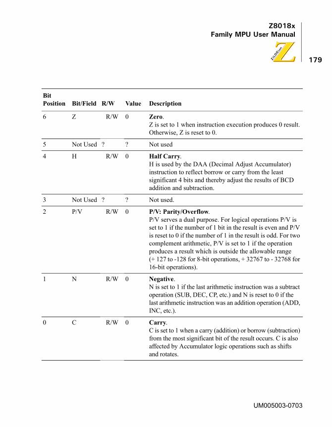
Z8018xFamily MPU User Manual
179
6 Z R/W 0 Zero.Z is set to 1 when instruction execution produces 0 result. Otherwise, Z is reset to 0.
5 Not Used ? ? Not used
4 H R/W 0 Half Carry.H is used by the DAA (Decimal Adjust Accumulator) instruction to reflect borrow or carry from the least significant 4 bits and thereby adjust the results of BCD addition and subtraction.
3 Not Used ? ? Not used.
2 P/V R/W 0 P/V: Parity/Overflow.P/V serves a dual purpose. For logical operations P/V is set to 1 if the number of 1 bit in the result is even and P/V is reset to 0 if the number of 1 in the result is odd. For two complement arithmetic, P/V is set to 1 if the operation produces a result which is outside the allowable range (+ 127 to -128 for 8-bit operations, + 32767 to - 32768 for 16-bit operations).
1 N R/W 0 Negative.N is set to 1 if the last arithmetic instruction was a subtract operation (SUB, DEC, CP, etc.) and N is reset to 0 if the last arithmetic instruction was an addition operation (ADD, INC, etc.).
0 C R/W 0 Carry.C is set to 1 when a carry (addition) or borrow (subtraction) from the most significant bit of the result occurs. C is also affected by Accumulator logic operations such as shifts and rotates.
BitPosition Bit/Field R/W Value Description
UM005003-0703

Z8018xFamily MPU User Manual
180
Addressing Modes
The Z80180 instruction set includes eight addressing modes.
• Implied Register
• Register Direct
• Register Indirect
• Indexed
• Extended
• Immediate
• Relative
• IO
Implied Register (IMP)
Certain Op Codes automatically imply register usage, such as the arithmetic operations that inherently reference the Accumulator, Index Registers, Stack Pointer, and General Purpose Registers.
Register Direct (REG)
Many Op Codes contain bit fields specifying registers used for operation. The exact bit field definitions vary depending on instruction depicted in Figure 75.
UM005003-0703

Z8018xFamily MPU User Manual
181
Figure 75. Register Direct — Bit Field Definitions
Register Indirect (REG)
The memory operand address is contained in one of the 16-bit General Purpose Registers (BC, DE, and HL) as illustrated in Figure 76.
Figure 76. Register Indirect Addressing
g or g field '8-bit Register
RegisterBCDEHL
A—
0 0 10 1 00 1 11 0 01 0 11 1 01 1 1
16-bit Registerzz field Register0 00 11 01 1
B CD EH LA F
ww field Register0 00 11 01 1
B CD EH LS P
xx field Register0 00 11 01 1
B CD EI XS P
yy field Register0 00 11 01 1
B CD EI YS P
0
Suffixed H and L ww,xx,yy,zz (ex. wwH,IXL) indicate upper and lower 8-bit of the 16-bit register respectively.
B CD EH L Operand
Memory
UM005003-0703

Z8018xFamily MPU User Manual
182
Indexed (INDX)
The memory operand address is calculated using the contents of an Index Register (IX or IY) and an 8-bit signed displacement specified in the instruction. Refer to Figure 77
Figure 77. Indexed Addressing
Extended (EXT)
The memory operand address is specified by two bytes contained in the instruction, as depicted in Figure 78.
Figure 78. Extended Addressing
Op Code 1
Operand
Memory
Op Code 2displacement (d)
IX or IY
Op Code
Operand
Memory
nm
m n
UM005003-0703
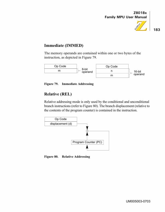
Z8018xFamily MPU User Manual
183
Immediate (IMMED)
The memory operands are contained within one or two bytes of the instruction, as depicted in Figure 79.
Figure 79. Immediate Addressing
Relative (REL)
Relative addressing mode is only used by the conditional and unconditional branch instructions (refer to Figure 80). The branch displacement (relative to the contents of the program counter) is contained in the instruction.
Figure 80. Relative Addressing
Op Codenm
m 16-bitoperand
Op Code8-bitoperand
Op Codedisplacement (d)
Program Counter (PC)
UM005003-0703

Z8018xFamily MPU User Manual
184
IO (I/O)
IO addressing mode is used only by I/O instructions. This mode specifies I/O address (IORQ is 0) and outputs them as follows.
1. An operand is output to A0–A7. The contents of accumulator is output to A8–A15.
2. The contents of Register B is output to A0–A7. The contents of Register C is output to A8–A15.
3. An operand is output to A0–A7. 00H is output to A8–A15 (useful for internal I/O register access)
4. The contents of Register C is output to A0–A7. 00H is output to A8–A15 (useful for internal I/O register access).
UM005003-0703

Z8018xFamily MPU User Manual
185
DC CharacteristicsThis section describes the DC characteristics of the Z8X180 family and absolute maximum rating for these products.
ABSOLUTE MAXIMUM RATING
Permanent IC damage may occur if maximum ratings are exceeded. Normal operation should be under recommended operating conditions. If these conditions are exceeded, it could affect reliability of IC.
Table 27. Absolute Maximum Rating
Item Symbol Value Unit
Supply Voltage Vcc - 0.3 � + 7.0 VInput Voltage Vin -0.3 � Vcc+0.3 VOperating Temperature Topr 0 � 70 °CExtended Temperature Text -40 � 85 °CStorage Temperature Tstg - 55 � +150 °C
UM005003-0703
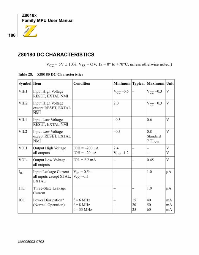
Z8018xFamily MPU User Manual
186
Z80180 DC CHARACTERISTICS
VCC = 5V � 10%, VSS = OV, Ta = 0� to +70�C, unless otherwise noted.)
Table 28. Z80180 DC Characteristics
Symbol Item Condition Minimum Typical Maximum Unit
VIH1 Input High Voltage RESET, EXTAL NMI
VCC –0.6 – VCC +0.3 V
VIH2 Input High Voltage except RESET, EXTAL NMI
2.0 VCC +0.3 V
VIL1 Input Low Voltage RESET, EXTAL NMI
–0.3 0.6 V
VIL2 Input Low Voltage except RESET, EXTAL NMI
–0.3 0.8Standard7 TLVIL
V
VOH Output High Voltageall outputs
IOH = –200 �AIOH = –20 �A
2.4VCC –1.2
––
––
VV
VOL Output Low Voltageall outputs
IOL = 2.2 mA – – 0.45 V
IIL Input Leakage Currentall inputs except XTAL, EXTAL
VIN = 0.5~VCC –0.5
– – 1.0 �A
ITL Three-State Leakage Current
– – 1.0 �A
ICC Power Dissipation*(Normal Operation)
f = 6 MHzf = 8 MHzf = 33 MHz
–––
152025
405060
mAmAmA
UM005003-0703
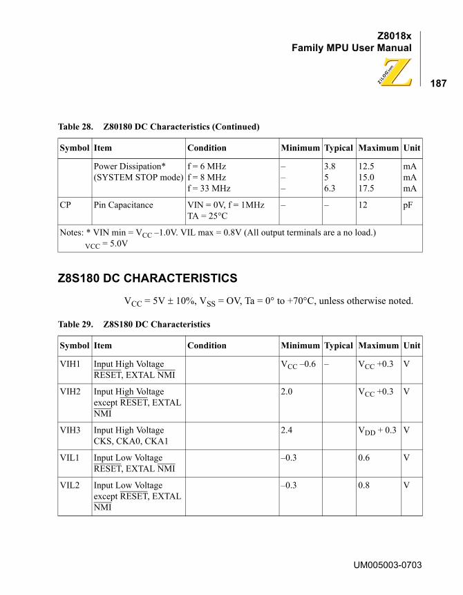
Z8018xFamily MPU User Manual
187
Z8S180 DC CHARACTERISTICS
VCC = 5V � 10%, VSS = OV, Ta = 0� to +70�C, unless otherwise noted.
Power Dissipation*(SYSTEM STOP mode)
f = 6 MHzf = 8 MHzf = 33 MHz
–––
3.856.3
12.515.017.5
mAmAmA
CP Pin Capacitance VIN = 0V, f = 1MHzTA = 25°C
– – 12 pF
Notes: * VIN min = VCC –1.0V. VIL max = 0.8V (All output terminals are a no load.)VCC = 5.0V
Table 29. Z8S180 DC Characteristics
Symbol Item Condition Minimum Typical Maximum Unit
VIH1 Input High Voltage RESET, EXTAL NMI
VCC –0.6 – VCC +0.3 V
VIH2 Input High Voltage except RESET, EXTAL NMI
2.0 VCC +0.3 V
VIH3 Input High Voltage CKS, CKA0, CKA1
2.4 VDD + 0.3 V
VIL1 Input Low Voltage RESET, EXTAL NMI
–0.3 0.6 V
VIL2 Input Low Voltage except RESET, EXTAL NMI
–0.3 0.8 V
Table 28. Z80180 DC Characteristics (Continued)
Symbol Item Condition Minimum Typical Maximum Unit
UM005003-0703
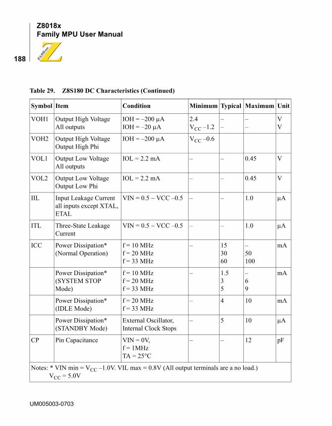
Z8018xFamily MPU User Manual
188
VOH1 Output High VoltageAll outputs
IOH = –200 �AIOH = –20 �A
2.4VCC –1.2
––
––
VV
VOH2 Output High VoltageOutput High Phi
IOH = –200 �A VCC –0.6
VOL1 Output Low VoltageAll outputs
IOL = 2.2 mA – – 0.45 V
VOL2 Output Low VoltageOutput Low Phi
IOL = 2.2 mA – – 0.45 V
IIL Input Leakage Currentall inputs except XTAL, ETAL
VIN = 0.5 ~ VCC –0.5 – – 1.0 �A
ITL Three-State Leakage Current
VIN = 0.5 ~ VCC –0.5 – – 1.0 �A
ICC Power Dissipation*(Normal Operation)
f = 10 MHzf = 20 MHzf = 33 MHz
– 153060
–50100
mA
Power Dissipation*(SYSTEM STOP Mode)
f = 10 MHzf = 20 MHzf = 33 MHz
– 1.535
–69
mA
Power Dissipation*(IDLE Mode)
f = 20 MHzf = 33 MHz
– 4 10 mA
Power Dissipation*(STANDBY Mode)
External Oscillator,Internal Clock Stops
– 5 10 �A
CP Pin Capacitance VIN = 0V,f = 1MHzTA = 25°C
– – 12 pF
Notes: * VIN min = VCC –1.0V. VIL max = 0.8V (All output terminals are a no load.)VCC = 5.0V
Table 29. Z8S180 DC Characteristics (Continued)
Symbol Item Condition Minimum Typical Maximum Unit
UM005003-0703

Z8018xFamily MPU User Manual
189
Z8L180 DC CHARACTERISTICS
VCC = 3.3V � 10%, VSS = OV, Ta = 0� to +70�C, unless otherwise noted.)
Table 30. Z8L180 DC Characteristics
Symbol Item Condition Minimum Typical Maximum Unit
VIH1 Input High Voltage RESET, EXTAL NMI
VCC –0.6 – VCC +0.3 V
VIH2 Input High Voltage except RESET, EXTAL NMI
2.0 VCC +0.3 V
VIL1 Input Low Voltage RESET, EXTAL NMI
–0.3 0.8 V
VIL2 Input Low Voltage except RESET, EXTAL NMI
–0.3 0.8 V
VOH1 Output High Voltageall outputs
IOH = –200 �A 2.4 V
VOH2 Output High VoltageOutput High Phi
IOH = –200 �A VCC –0.6 V
VOL Output Low Voltageall outputs
IOL = 4 mA – – 0.4 V
VOL2 Output Low VoltageOutput Low Phi
IOL = 4 mA – – 0.4 V
IIL Input Leakage Currentall inputs except XTAL, EXTAL
VIN = 0.5 ~ VCC –0.5 – – 1.0 �A
ITL Three-State Leakage Current
VIN = 0.5 ~ VCC –0.5 – – 1.0 �A
UM005003-0703
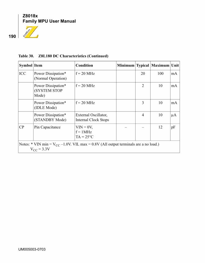
Z8018xFamily MPU User Manual
190
ICC Power Dissipation*(Normal Operation)
f = 20 MHz 20 100 mA
Power Dissipation*(SYSTEM STOP Mode)
f = 20 MHz 2 10 mA
Power Dissipation*(IDLE Mode)
f = 20 MHz 3 10 mA
Power Dissipation*(STANDBY Mode)
External Oscillator,Internal Clock Stops
4 10 �A
CP Pin Capacitance VIN = 0V,f = 1MHzTA = 25°C
– – 12 pF
Notes: * VIN min = VCC –1.0V. VIL max = 0.8V (All output terminals are a no load.)VCC = 3.3V
Table 30. Z8L180 DC Characteristics (Continued)
Symbol Item Condition Minimum Typical Maximum Unit
UM005003-0703

Z8018xFamily MPU User Manual
191
5
4
3
2
1
2.7 3.0 3.3VDD (Volts)
I CC
Act
ive
(mA
.)
Typical ICCA at 4 MHz
Z8L180
50
40
30
20
10
2 3 4
VDD (Volts)
I CC
Act
ive
(mA
.)
Typical ICCA at 20 MHz
Z8S180
5
UM005003-0703

Z8018xFamily MPU User Manual
192
UM005003-0703

Z8018xFamily MPU User Manual
193
AC CharacteristicsThis section describes the AC characteristics of the Z8X180 family and absolute maximum rating for these products.
AC CHARACTERISTICS—Z8S180
Table 31. Z8S180 AC Characteristics VDD = 5V ±10% or VDD = 3.3V ±10%; 33-MHz Characteristics Apply Only to 5V Operation
No. Symbol Item
Z8S180—20 MHz
Z8S180—33 MHz
UnitMin Max Min Max
1 tCYC Clock Cycle Time 50 DC 30 DC ns2 tCHW Clock “H” Pulse Width 15 — 10 — ns3 tCLW Clock “L” Pulse Width 15 — 10 — ns4 tCF Clock Fall Time — 10 — 5 ns5 tCR Clock Rise Time — 10 — 5 ns6 tAD PHI Rise to Address Valid Delay — 30 — 15 ns7 tAS Address Valid to MREQ Fall or
IORQ Fall)5 — 5 — ns
8 tMED1 PHI Fall to MREQ Fall Delay — 25 — 15 ns9 tRDD1 PHI Fall to RD Fall Delay IOC = 1 — 25 — 15 ns
PHI Rise to RD Rise Delay IOC = 0
— 25 — 15
10 tM1D1 PHI Rise to M1 Fall Delay — 35 — 15 ns11 tAH Address Hold Time from
MREQ, IOREQ, RD, WR High5 — 5 — ns
UM005003-0703

Z8018xFamily MPU User Manual
194
12 tMED2 PHI Fall to MREQ Rise Delay — 25 — 15 ns13 tRDD2 PHI Fall to RD Rise Delay — 25 — 15 ns14 tM1D2 PHI Rise to M1 Rise Delay — 40 — 15 ns15 tDRS Data Read Set-up Time 10 — 5 — ns16 tDRH Data Read Hold Time 0 — 0 — ns17 tSTD1 PHI Fall to ST Fall Delay — 30 — 15 ns18 tSTD2 PHI Fall to ST Rise Delay — 30 — 15 ns19 tWS WAIT Set-up Time to PHI Fall 15 — 10 — ns20 tWH WAIT Hold Time from PHI Fall 10 — 5 — ns21 tWDZ PHI Rise to Data Float Delay — 35 — 20 ns22 tWRD1 PHI Rise to WR Fall Delay — 25 — 15 ns23 tWDD PHI Fall to Write Data Delay Time — 25 — 15 ns24 tWDS Write Data Set-up Time to WR Fall 10 — 10 — ns25 tWRD2 PHI Fall to WR Rise Delay — 25 — 15 ns26 tWRP WR Pulse Width (Memory Write
Cycle)80 — 45 — ns
26a WR Pulse Width (I/O Write Cycle) 150 — 70 — ns27 tWDH Write Data Hold Time from WR Rise 10 — 5 — ns28 tIOD1 PHI Fall to IORQ Fall Delay IOC
= 1— 25 — 15 ns
PHI Rise to IORQ Fall Delay IOC = 0
— 25 — 15
29 tIOD2 PHI Fall to IORQ Rise Delay — 25 — 15 ns30 tIOD3 M1 Fall to IORQ Fall Delay 125 — 80 — ns
Table 31. Z8S180 AC Characteristics (Continued) VDD = 5V ±10% or VDD = 3.3V ±10%; 33-MHz Characteristics Apply Only to 5V Operation
No. Symbol Item
Z8S180—20 MHz
Z8S180—33 MHz
UnitMin Max Min Max
UM005003-0703

Z8018xFamily MPU User Manual
195
31 tINTS INT Set-up Time to PHI Fall 20 — 15 — ns32 tINTH INT Hold Time from PHI Fall 10 — 10 — ns33 tNMIW NMI Pulse Width 35 — 25 — ns34 tBRS BUSREQ Set-up Time to PHI Fall 10 — 10 — ns35 tBRH BUSREQ Hold Time from PHI Fall 10 — 10 ns36 tBAD1 PHI Rise to BUSACK Fall Delay — 25 — 15 ns37 tBAD2 PHI Fall to BUSACK Rise Delay — 25 — 15 ns38 tBZD PHI Rise to Bus Floating Delay Time — 40 — 30 ns39 tMEWH MREQ Pulse Width (High) 35 — 25 — ns40 tMEWL MREQ Pulse Width (Low) 35 — 25 — ns41 tRFD1 PHI Rise to RFSH Fall Delay — 20 — 15 ns42 tRFD2 PHI Rise to RFSH Rise Delay — 20 — 15 ns43 tHAD1 PHI Rise to HALT Fall Delay — 15 — 15 ns44 tHAD2 PHI Rise to HALT Rise Delay — 15 — 15 ns45 tDRQS DREQ1 Set-up Time to PHI Rise 20 — 15 — ns46 tDRQH DREQ1 Hold Time from PHI Rise 20 — 15 — ns47 tTED1 PHI Fall to TENDi Fall Delay — 25 — 15 ns48 tTED2 PHI Fall to TENDi Rise Delay — 25 — 15 ns49 tED1 PHI Rise to E Rise Delay — 30 — 15 ns50 tED2 PHI Fall or Rise to E Fall Delay — 30 — 15 ns51 PWEH E Pulse Width (High) 25 — 20 — ns52 PWEL E Pulse Width (Low) 50 — 40 — ns53 tEr Enable Rise Time — 10 — 10 ns
Table 31. Z8S180 AC Characteristics (Continued) VDD = 5V ±10% or VDD = 3.3V ±10%; 33-MHz Characteristics Apply Only to 5V Operation
No. Symbol Item
Z8S180—20 MHz
Z8S180—33 MHz
UnitMin Max Min Max
UM005003-0703
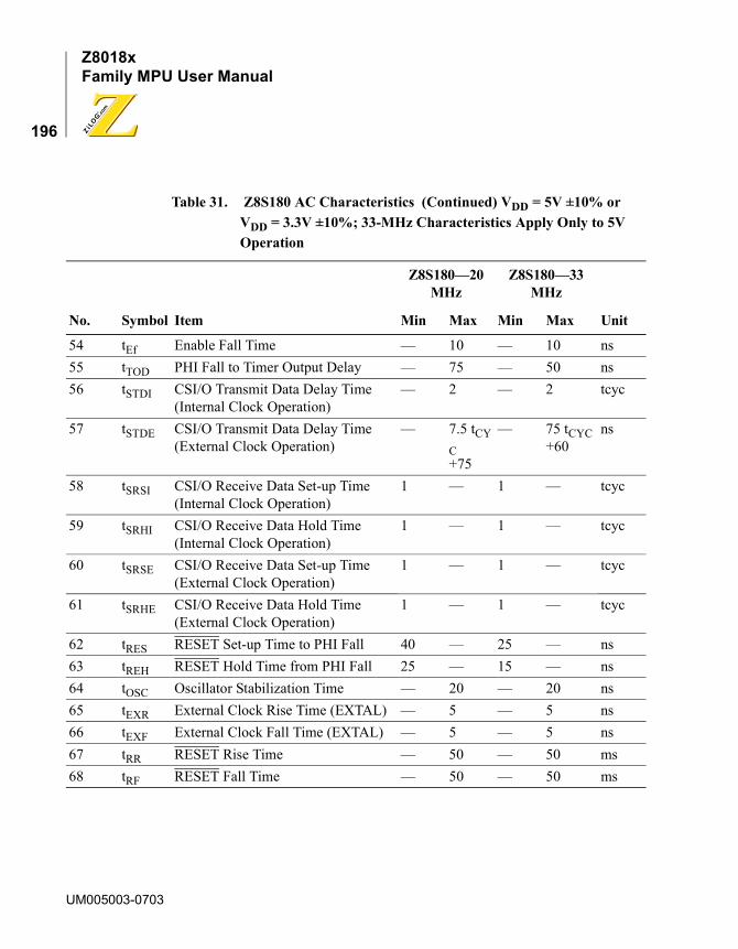
Z8018xFamily MPU User Manual
196
54 tEf Enable Fall Time — 10 — 10 ns55 tTOD PHI Fall to Timer Output Delay — 75 — 50 ns56 tSTDI CSI/O Transmit Data Delay Time
(Internal Clock Operation)— 2 — 2 tcyc
57 tSTDE CSI/O Transmit Data Delay Time (External Clock Operation)
— 7.5 tCYC+75
— 75 tCYC+60
ns
58 tSRSI CSI/O Receive Data Set-up Time (Internal Clock Operation)
1 — 1 — tcyc
59 tSRHI CSI/O Receive Data Hold Time (Internal Clock Operation)
1 — 1 — tcyc
60 tSRSE CSI/O Receive Data Set-up Time (External Clock Operation)
1 — 1 — tcyc
61 tSRHE CSI/O Receive Data Hold Time (External Clock Operation)
1 — 1 — tcyc
62 tRES RESET Set-up Time to PHI Fall 40 — 25 — ns63 tREH RESET Hold Time from PHI Fall 25 — 15 — ns64 tOSC Oscillator Stabilization Time — 20 — 20 ns65 tEXR External Clock Rise Time (EXTAL) — 5 — 5 ns66 tEXF External Clock Fall Time (EXTAL) — 5 — 5 ns67 tRR RESET Rise Time — 50 — 50 ms68 tRF RESET Fall Time — 50 — 50 ms
Table 31. Z8S180 AC Characteristics (Continued) VDD = 5V ±10% or VDD = 3.3V ±10%; 33-MHz Characteristics Apply Only to 5V Operation
No. Symbol Item
Z8S180—20 MHz
Z8S180—33 MHz
UnitMin Max Min Max
UM005003-0703
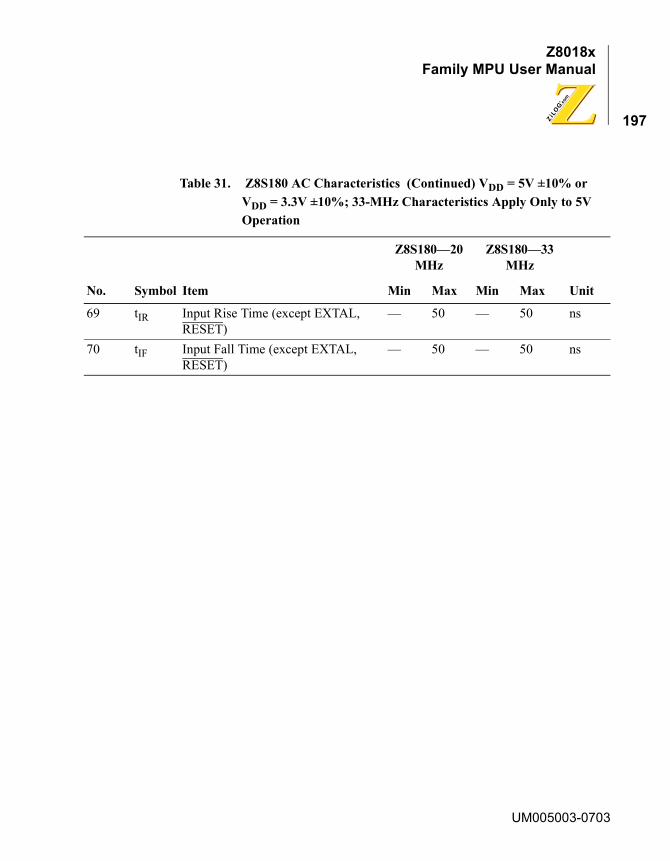
Z8018xFamily MPU User Manual
197
69 tIR Input Rise Time (except EXTAL, RESET)
— 50 — 50 ns
70 tIF Input Fall Time (except EXTAL, RESET)
— 50 — 50 ns
Table 31. Z8S180 AC Characteristics (Continued) VDD = 5V ±10% or VDD = 3.3V ±10%; 33-MHz Characteristics Apply Only to 5V Operation
No. Symbol Item
Z8S180—20 MHz
Z8S180—33 MHz
UnitMin Max Min Max
UM005003-0703
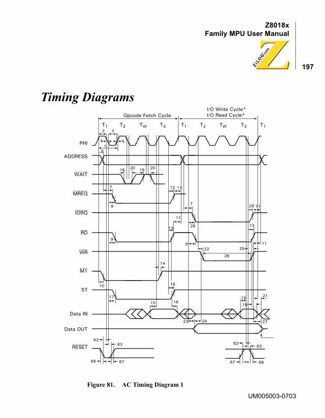
Z8018xFamily MPU User Manual
197
Timing Diagrams
Figure 81. AC Timing Diagram 1
PHI
ADDRESS
WAIT
MREQ
IORQ
RD
WR
M1
ST
Data IN
Data OUT
RESET
11
67 68
6263
68 67
6263
15 1617
10
14
9
22
13
11
28
7 29
7
8
2019 1920
1112
6
9
13
2511
Opcode Fetch Cycle
T1
1
2 3
4 5
15
16
21
27
18
I/O Write Cycle*I/O Read Cycle*
T2 TW T3 T1 T2 TW T3 T1
23 24
26
UM005003-0703

Z8018xFamily MPU User Manual
198
UM005003-0703
Memory Read/Write Cycle timing is the sam as I/O Read/Write Cycle except there are no automatica Wait States (TW), and MREQ is active instead of IORQ.
Figure 82. AC Timing Diagram 2
PHI
INT0,1,2
3132
33
40
3028
1516
29
39
41 42
3435 34 35
36 37
38 38
43 44
1410
NMI
M1
IORQ
Data IN
MREQ
RFSH
BUSREQ
BUSACK
MREQ, RDWR, IORQ
HALT
Output Buffer Off
A19–0, D7–0

Z8018xFamily MPU User Manual
199
Figure 83. CPU Timing (IOC = 0) (I/O Read Cycle, I/O Write Cycle)
T1 T2 Tw T3 T1 T2 Tw T3
ADDRESS
PHI
RD
IORQ
WR
28
9
2928 29
13
22 25
I/O Read Cycle I/O Write Cycle
CPU Timing (IOC = 0)I/O Read CycleI/O Write Cycle
UM005003-0703
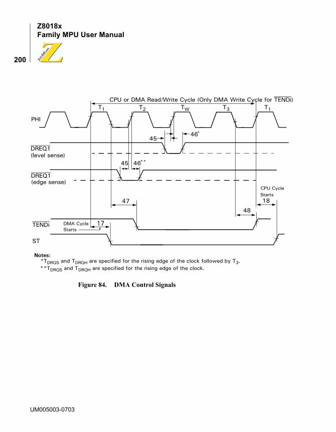
Z8018xFamily MPU User Manual
200
Figure 84. DMA Control Signals
47
45 46
48
18
(level sense)
DREQ1(edge sense)
TENDi
ST
PHI
T1 T2 TW T3 T1
17
DREQ1
CPU or DMA Read/Write Cycle (Only DMA Write Cycle for TENDi)
4546*
**
CPU CycleStarts
DMA CycleStarts
Notes:*TDRQS and TDRQH are specified for the rising edge of the clock followed by T3. **TDRQS and TDRQH are specified for the rising edge of the clock.
UM005003-0703
Z8018xFamily MPU User Manual
201
Figure 85. E Clock Timing (Memory R/W Cycle) (I/O R/W Cycle)
Figure 86. E Clock Timing (BUS RELEASE Mode, SLEEP Mode, and SYSTEM STOP Mode
49
49
49
15
50
50
50
16
D0–D7
E(Memory Read/Write)
E(I/O Read)
E(I/O Write)
PHI
~~~~
~~~~
~~~~
T1 T2 TW TW T3
PHIEBUS RELEASE modeSLEEP modeSYSTEM STOP mode
49 50
UM005003-0703
Z8018xFamily MPU User Manual
202
Figure 87. E Clock Timing (Minimum Timing Example of PWEL and PWEH)
Figure 88. Timer Output Timing
5052
53
49 53
T2T2 TW T3 T1
54
49
51
54
50EExampleI/O Read� Opcode Fetch
PHI
E(I/O Write)
55
Timer DataReg. = 0000H
A18/TOUT
PHI
UM005003-0703
Z8018xFamily MPU User Manual
203
Figure 89. SLP Execution Cycle Timing Diagram
32
4443
33
A19–A0
SLP Instruction Fetch
MREQ, M1
NMI
INTi
HALT
PHI
~~~~
~~~~
~~
T1 T2 TS TST3 T1 T2
31
RD
Next Opcode Fetch
~~~~
UM005003-0703
Z8018xFamily MPU User Manual
204
Figure 90. CSI/O Receive/Transmit Timing Diagram
Figure 91. External Clock Rise Time and Fall Time
Figure 92. Input Rise Time and Fall Time (Except EXTAL, RESET)
57
56
58
56
11.5tcyc
Transmit Data
5958 59
11.5tcyc
11tcyc
16.5tcyc
11tcyc
16.5tcyc
57
60 6160 61
(External Clock)
Transmit Data(Internal Clock)
Receive Data(External Clock)
Receive Data(Internal Clock)
CSI/O Clock
EXTAL VIL1 VIH1 VIL1VIH1
65 66
70 69
UM005003-0703

Z8018xFamily MPU User Manual
205
STANDARD TEST CONDITIONS
The previous DC Characteristics and Capacitance sections apply to the following standard test conditions, unless otherwise noted. All voltages are referenced to GND (0V). Positive current flows in to the referenced pin.
All AC parameters assume a load capacitance of 100 pF. Add 10 ns delay for each 50 pF increase in load up to a maximum of 200 pF for the data bus and 100 pF for the address and control lines. AC timing measurements are referenced to 1.5 volts (except for CLOCK, which is referenced to the 10% and 90% points).
The Ordering Information section lists temperature ranges and product numbers. Package drawings are in the Package Information section. Refer to the Literature List for additional documentation.
Figure 93. Test Setup
+5V
2.1K�
100 pf
From OutputUnder Test
200�Av
UM005003-0703

Z8018xFamily MPU User Manual
206
UM005003-0703
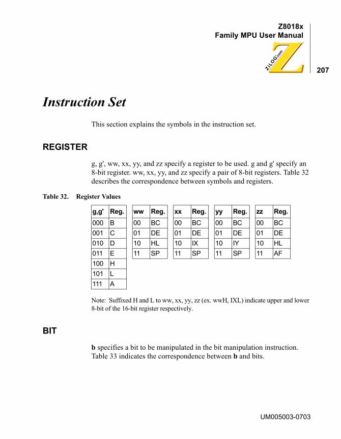
Z8018xFamily MPU User Manual
207
Instruction SetThis section explains the symbols in the instruction set.
REGISTER
g, g', ww, xx, yy, and zz specify a register to be used. g and g' specify an 8-bit register. ww, xx, yy, and zz specify a pair of 8-bit registers. Table 32 describes the correspondence between symbols and registers.
Note: Suffixed H and L to ww, xx, yy, zz (ex. wwH, IXL) indicate upper and lower 8-bit of the 16-bit register respectively.
BIT
b specifies a bit to be manipulated in the bit manipulation instruction. Table 33 indicates the correspondence between b and bits.
Table 32. Register Values
g,g' Reg. ww Reg. xx Reg. yy Reg. zz Reg.000 B 00 BC 00 BC 00 BC 00 BC001 C 01 DE 01 DE 01 DE 01 DE010 D 10 HL 10 IX 10 IY 10 HL011 E 11 SP 11 SP 11 SP 11 AF100 H101 L111 A
UM005003-0703
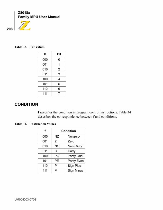
Z8018xFamily MPU User Manual
208
CONDITION
f specifies the condition in program control instructions. Table 34 describes the correspondence between f and conditions.
Table 33. Bit Values
b Bit000 0001 1010 2011 3100 4101 5110 6111 7
Table 34. Instruction Values
f Condition000 NZ Nonzero001 Z Zero010 NC Non Carry011 C Carry100 PO Parity Odd101 PE Parity Even110 P Sign Plus111 M Sign Minus
UM005003-0703

Z8018xFamily MPU User Manual
209
RESTART ADDRESS
v specifies a restart address. Table 35 describes the correspondence between v and restart addresses.
FLAG
The symbols listed in Table 36 indicate the flag conditions.
Table 35. Address Values
v Address000 00H001 08H010 l0H011 18H100 20H101 28H110 30H111 38H
Table 36. Flag Conditions
� Not Affected� Affectedx UndefinedS Set to 1R Reset to 0P ParityV Overflow
UM005003-0703

Z8018xFamily MPU User Manual
210
MISCELLANEOUS
Table 37 lists the operations mnemonics.
Table 37. Operations Mnemonics
( )M Data in the memory address( )I Data in the I/O addressm or n 8-bit datamn 16-bit datar 8-bit registerR 16-bit registerb.( )M A content of bit b in the memory addressb.gr A content of bit b in the register grd or j 8-bit signed displacementS SourceD Destination� AND operation+ OR operation� EXCLUSIVE OR operation** Added new instructions to Z80
UM005003-0703

Z8018xFamily MPU User Manual
211
DATA MANIPULATION INSTRUCTIONS
Table 38. Arithmetic and Logical Instructions (8-bit)
OperationName Mnemonics Op Code
Addressing
Bytes States Operation
Flags
7 6 4 2 1 0
Immed Ext Ind Reg RegI Imp Rel S Z H P/V N C
ADD ADD A,g 10 000 g S D 1 4 Ar + gr�Ar � � � V R �
ADD A, (HL) 10 000 110 S D 1 6 Ar + (HL)M�Ar � � � V R �
ADD A, m 11 000 110 S D 2 6 Ar + m�Ar � � � V R �
�m�
ADD A,(IX + d) 11 011 101 S D 3 14 Ar + (IX + d)M�Ar � � � V R �
10 000 110
�d�
ADD A,(IY + d) 11 111 101 S D 3 14 Ar + (IY + d))M�Ar � � � V R �
10 000 I10
�d�
ADC ADC A,g 10 001 g S D 1 4 Ar + gr + c�Ar � � � V R �
ADC A,(HL) 10 001 110 S D 1 6 Ar + (HL)M + c�Ar � � � V R �
ADC A,m 11 001 110 S D 2 6 Ar + m + c�Ar � � � V R �
�m�
ADC A,(IX + d) 11 011 101 S D 3 14 Ar + (lX + d))M + c�Ar
� � � V R �
10 001 110
�d�
ADC A,(IY + d) 11 111 101 S D 3 14 Ar + (IY + d))M + c�Ar
� � � V R �
10 001 110
�d�
UM005003-0703
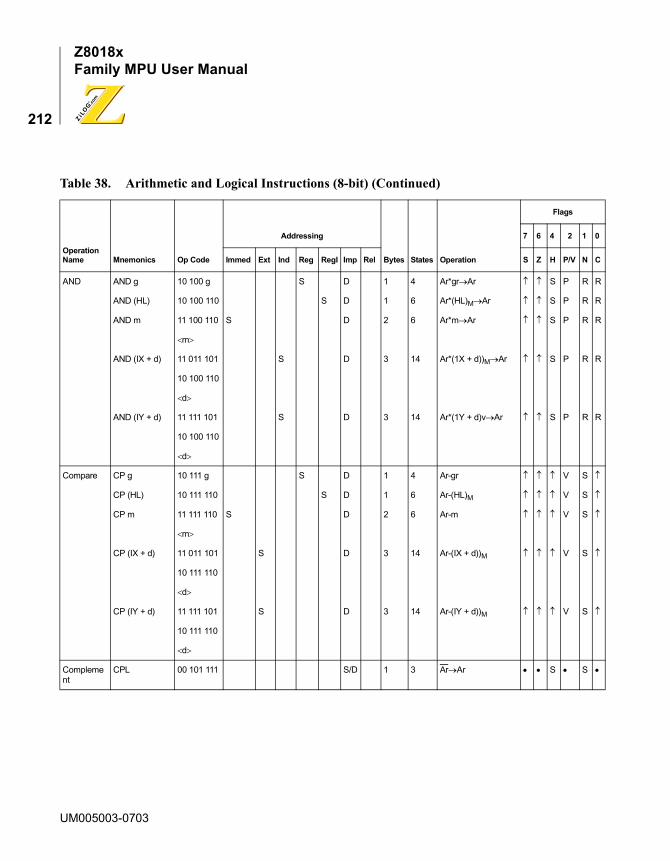
Z8018xFamily MPU User Manual
212
AND AND g 10 100 g S D 1 4 Ar*gr�Ar � � S P R R
AND (HL) 10 100 110 S D 1 6 Ar*(HL)M�Ar � � S P R R
AND m 11 100 110 S D 2 6 Ar*m�Ar � � S P R R
�m�
AND (IX + d) 11 011 101 S D 3 14 Ar*(1X + d))M�Ar � � S P R R
10 100 110
�d�
AND (IY + d) 11 111 101 S D 3 14 Ar*(1Y + d)v�Ar � � S P R R
10 100 110
�d�
Compare CP g 10 111 g S D 1 4 Ar-gr � � � V S �
CP (HL) 10 111 110 S D 1 6 Ar-(HL)M � � � V S �
CP m 11 111 110 S D 2 6 Ar-m � � � V S �
�m�
CP (IX + d) 11 011 101 S D 3 14 Ar-(IX + d))M � � � V S �
10 111 110
�d�
CP (IY + d) 11 111 101 S D 3 14 Ar-(IY + d))M � � � V S �
10 111 110
�d�
Complement
CPL 00 101 111 S/D 1 3 Ar�Ar � � S � S �
Table 38. Arithmetic and Logical Instructions (8-bit) (Continued)
OperationName Mnemonics Op Code
Addressing
Bytes States Operation
Flags
7 6 4 2 1 0
Immed Ext Ind Reg RegI Imp Rel S Z H P/V N C
UM005003-0703
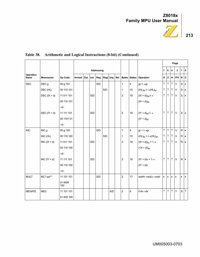
Z8018xFamily MPU User Manual
213
DEC DEC g 00 g 101 S/D 1 4 gr-1�gr � � � V S �
DEC (HL) 00 110 101 S/D 1 10 (HL)M-1�(HL)M � � � V S �
DEC (IX + d) 11 011 101 S/D 3 18 (IX + d))M-I� � � � V S �
00 110 101 (IX + d))M
�d�
DEC (IY + d) 11 111 101 S/D 3 18 (IY + d)M-1� � � � V S �
00 1101 01 (IY + d)M
�d�
INC INC g 00 g 100 S/D 1 4 gr + I�gr � � � V R �
INC (HL) 00 110 100 S/D 1 10 (HL)M + I�(HL)M � � � V R �
INC (IX + d) 11 011 101 S/D 3 18 (IX + d))M + 1� � � � V R �
00 110 100 (1X + d))M
�d�
INC (IY + d) 11 111 101 S/D 3 18 (IY + d)v + 1� � � � V R �
00 110 100 (IY + d)v
�d�
MULT MLT ww** 11 101 101 S/D 2 17 wwHr�wwLr�wwI � � � � � �
01 WWI 100
NEGATE NEG 11 101 101 S/D 2 6 0-Ar�Ar � � � Y S �
01 000 100
Table 38. Arithmetic and Logical Instructions (8-bit) (Continued)
OperationName Mnemonics Op Code
Addressing
Bytes States Operation
Flags
7 6 4 2 1 0
Immed Ext Ind Reg RegI Imp Rel S Z H P/V N C
UM005003-0703

Z8018xFamily MPU User Manual
214
OR OR g 10 110 g S D 1 4 Ar + gr�Ar � � R P R R
OR (HL) 10 110 110 S D 1 6 Ar + (HL)M�Ar � � R P R R
OR m 11 110 110 S D 2 6 Ar + m�Ar � � R P R R
�m�
OR (IX + d) 11 011 101 S D 3 14 Ar + (IX + d)M�Ar � � R P R R
10 110 110
�d�
OR (IY + d) 11 111 101 S D 3 14 Ar + (IY + d)M�Ar � � R P R R
10 110 110
�d�
SUB SUB g 10 010 g S D 1 4 Ar-gr�Ar � � � V S �
SUB (HL) 10 010 110 S D 1 6 Ar-(HL)M�Ar � � � V S �
SUB m 11 010 110 S D 2 6 Ar-m�Ar � � � V S �
�m�
SUB (IX + d) 11 011 101 S D 3 14 Ar-(IX + d)M-c�Ar � � � V S �
10 011 110
�d�
SUB (IY + d) 11 111 101 S D 3 14 Ar-(IY + d)M-c�Ar � � � V S �
10 010 110
�d�
Table 38. Arithmetic and Logical Instructions (8-bit) (Continued)
OperationName Mnemonics Op Code
Addressing
Bytes States Operation
Flags
7 6 4 2 1 0
Immed Ext Ind Reg RegI Imp Rel S Z H P/V N C
UM005003-0703
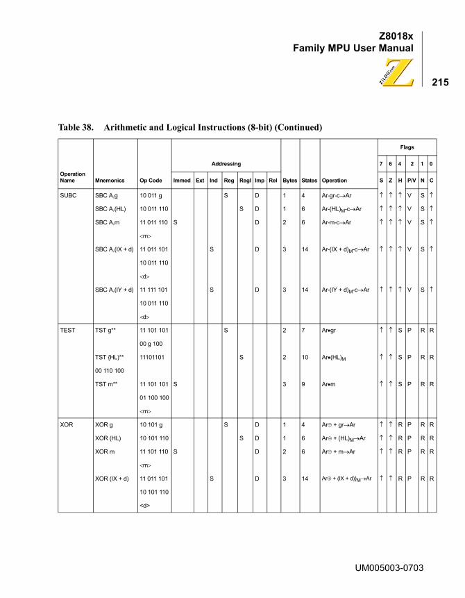
Z8018xFamily MPU User Manual
215
SUBC SBC A,g 10 011 g S D 1 4 Ar-gr-c�Ar � � � V S �
SBC A,(HL) 10 011 110 S D 1 6 Ar-(HL)M-c�Ar � � � V S �
SBC A,m 11 011 110 S D 2 6 Ar-m-c�Ar � � � V S �
�m�
SBC A,(IX + d) 11 011 101 S D 3 14 Ar-(IX + d)M-c�Ar � � � V S �
10 011 110
�d�
SBC A,(IY + d) 11 111 101 S D 3 14 Ar-(IY + d)M-c�Ar � � � V S �
10 011 110
�d�
TEST TST g** 11 101 101 S 2 7 Ar�gr � � S P R R
00 g 100
TST {HL)** 11101101 S 2 10 Ar�(HL)M � � S P R R
00 110 100
TST m** 11 101 101 S 3 9 Ar�m � � S P R R
01 100 100
�m�
XOR XOR g 10 101 g S D 1 4 Ar� + gr�Ar � � R P R R
XOR (HL) 10 101 110 S D 1 6 Ar� + (HL)M�Ar � � R P R R
XOR m 11 101 110 S D 2 6 Ar� + m�Ar � � R P R R
�m�
XOR (IX + d) 11 011 101 S D 3 14 Ar� + (IX + d))M�Ar � � R P R R
10 101 110
<d>
Table 38. Arithmetic and Logical Instructions (8-bit) (Continued)
OperationName Mnemonics Op Code
Addressing
Bytes States Operation
Flags
7 6 4 2 1 0
Immed Ext Ind Reg RegI Imp Rel S Z H P/V N C
UM005003-0703

Z8018xFamily MPU User Manual
216
0
C
�
�
�
�
�
�
�
�
XOR (IY + d) 11 111 101 S D 3 14 Ar� + (IY + d))M�Ar � � R P R R
10 101 110
<d>
Table 39. Rotate and Shift Instructions
OperationName Mnemonics Op Code
Addressing
BytesStates Operation
Flags
7 6 4 2 1
Immed Ext Ind Reg Regi Imp Rel S Z H P/V N
Rotate andShiftData
RL A 00 010 1111 S/D 1 3 � � R � R
RL g 11 001 011 S/D 2 7 � � R P R
00 010 g
RL (HL) 11 001 011 S/D 2 13 � � R P R
00 010 110
RL (IX + d) 11 011 101 S/D 4 19 � � R P R
11 001 011
�d�
00 010 110
RL (IY + d) 11 111 101 S/D 4 19 � � R P R
11 001 011
�d�
00 010 110
RLC A 00 000 111 S/D 1 3 � � R � R
RLC g 11 001 011 S/D 2 7 � � R P R
00 000 g
RLC (HL) 11 001 011 S/D 2 13 � � R P R
00 000 110
Table 38. Arithmetic and Logical Instructions (8-bit) (Continued)
OperationName Mnemonics Op Code
Addressing
Bytes States Operation
Flags
7 6 4 2 1 0
Immed Ext Ind Reg RegI Imp Rel S Z H P/V N C
C b7 b0
b7 b0
b7 b0
Ar
(HL)M
Cb7 b0
UM005003-0703

Z8018xFamily MPU User Manual
217
�
�
�
�
�
�
�
�
�
�
�
�
�
0
C
RLC (IX + d) 11 011 101 S/D 4 19 � � R P R
11 001 011
�d�
00 000 110
RLC (IY + d) 11 111 101 S/D 4 19 � � R P R
11 001 011
�d�
00 000 110
RLD 11 101 101 S/D 2 16 � � R P R
01 101 111
RRA 00 011 111 S/D 1 3 � � R � R
RRg 11 001 011 S/D 2 7 � � R P R
00 011 g
RR (HL) 11 001 011 S/D 2 13 � � R P R
00 011 110
RR (IX + d) 11 011 101 S/D 4 19 � � R P R
11 001 011
�d�
00 011 110
RR (IY + d) 11 111 101 S/D 4 19 � � R P R
11 001 011
�d�
00 011 110
RRCA 00 001 111 S/D 1 3 � � R � R
RRC g 11 001 011 S/D 2 7 � � R P R
00 001 g
RRC (HL) 11 001 011 S/D 2 13 � � R P R
00 001 110
RRC (IX + d) 11 011 101 S/D 4 19 � � R P R
11 001 011
�d�
00 001 110
RRC (IY + d) 11 111 101 S/D 4 19 � � R P R
Table 39. Rotate and Shift Instructions (Continued)
OperationName Mnemonics Op Code
Addressing
BytesStates Operation
Flags
7 6 4 2 1
Immed Ext Ind Reg Regi Imp Rel S Z H P/V N
Cb7b0
C b7 b0
UM005003-0703
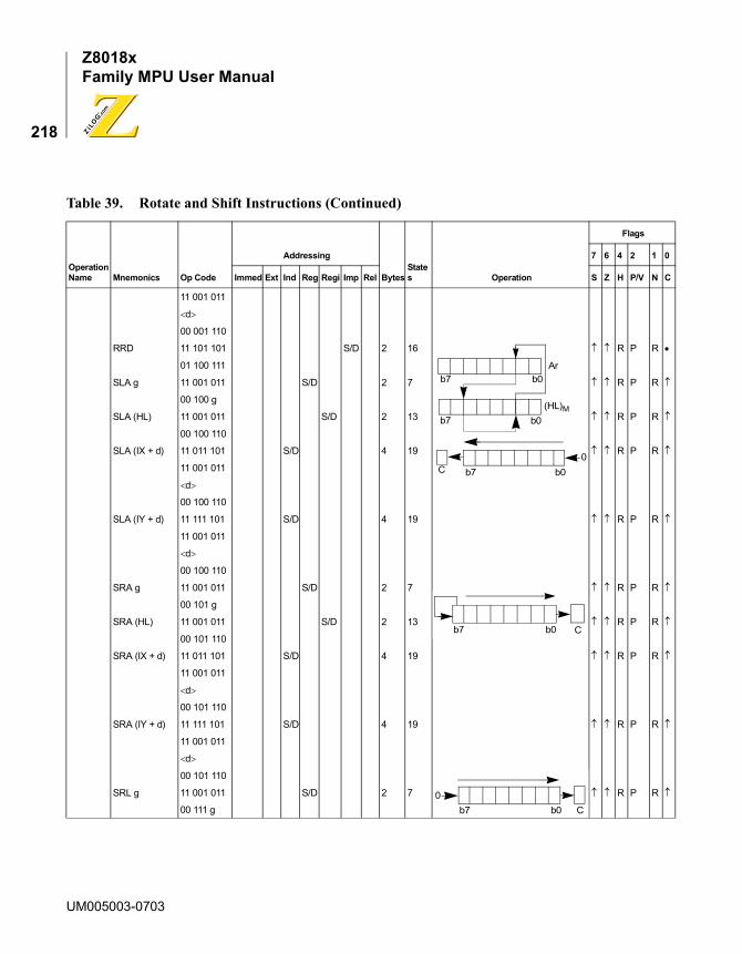
Z8018xFamily MPU User Manual
218
�
�
�
�
�
�
�
�
�
�
0
C
11 001 011
�d�
00 001 110
RRD 11 101 101 S/D 2 16 � � R P R
01 100 111
SLA g 11 001 011 S/D 2 7 � � R P R
00 100 g
SLA (HL) 11 001 011 S/D 2 13 � � R P R
00 100 110
SLA (IX + d) 11 011 101 S/D 4 19 � � R P R
11 001 011
�d�
00 100 110
SLA (IY + d) 11 111 101 S/D 4 19 � � R P R
11 001 011
�d�
00 100 110
SRA g 11 001 011 S/D 2 7 � � R P R
00 101 g
SRA (HL) 11 001 011 S/D 2 13 � � R P R
00 101 110
SRA (IX + d) 11 011 101 S/D 4 19 � � R P R
11 001 011
�d�
00 101 110
SRA (IY + d) 11 111 101 S/D 4 19 � � R P R
11 001 011
�d�
00 101 110
SRL g 11 001 011 S/D 2 7 � � R P R
00 111 g
Table 39. Rotate and Shift Instructions (Continued)
OperationName Mnemonics Op Code
Addressing
BytesStates Operation
Flags
7 6 4 2 1
Immed Ext Ind Reg Regi Imp Rel S Z H P/V N
b7 b0Ar
(HL)M
C b7 b00
b7 b0
Cb7 b0
Cb7 b00
UM005003-0703

Z8018xFamily MPU User Manual
219
�
�
�
�
�
�
�
�
�
�
0
C
SRL (HL) 11 001 011 S/D 2 3 � � R P R
00 111 110
SRL (IX + d) 11 011 101 S/D 4 19 � � R P R
11 001 011
�d�
00 111 110
SRL (IY + d) 11 111 101 S/D 4 19 � � R P R
11 001 011
�d�
00 111 110
Bit Set SET b,g 11 001 011 S/D 2 7 1�b�gr � � � � �
11 b g
SET b,(HL) 11 001 011 S/D 2 13 1�b�(HL)M � � � � �
11 b 110
SET b,(IX + d) 11 011 101 S/D 4 19 1�b�(IX + d)M � � � � �
11 001 011
�d�
11 b 110
SET b,(IY + d) 11 111 101 S/D 4 19 l �b�(IY + d)M � � � � �
11 001 011
�d�
11 b 110
Bit Reset RES b,g 11 001 011 S/D 2 7 0 �b�gr � � � � �
10 b g
RES b,(HL) 11 001 011 S/D 2 13 0 �6*b�(HL)M � � � � �
10 b 110
RES b,(IX + d) 11 011 101 S/D 4 19 0 ��b�(IX + d)M � � � � �
11 001 011
�d�
10 b 110
Table 39. Rotate and Shift Instructions (Continued)
OperationName Mnemonics Op Code
Addressing
BytesStates Operation
Flags
7 6 4 2 1
Immed Ext Ind Reg Regi Imp Rel S Z H P/V N
UM005003-0703

Z8018xFamily MPU User Manual
220
�
�
�
�
�
0
C
Bit Reset RES b,(IY + d) 11 011 101 S/D 4 19 0�b�(IY + d)M � � � � �
11 001 01l
�d�
10 b 110
Bit Test BIT b, g 11 001 011 S 2 6 b�gr�z X � S X R
01bg
BIT b,(HL) 11 001 011 S 2 9 b�(HL)M�z X � S X R
01 b 110
BIT b,(IX + d) 11 011 101 S 4 15 b�(IX + d)M�z X � S X R
11 001 011
�d�
01 b 110
BIT b,(IY + d) 11 111 101 S 4 15 b�(IY + d)M�z X � S X R
11 001 011
�d�
01 b 110
Table 39. Rotate and Shift Instructions (Continued)
OperationName Mnemonics Op Code
Addressing
BytesStates Operation
Flags
7 6 4 2 1
Immed Ext Ind Reg Regi Imp Rel S Z H P/V N
UM005003-0703
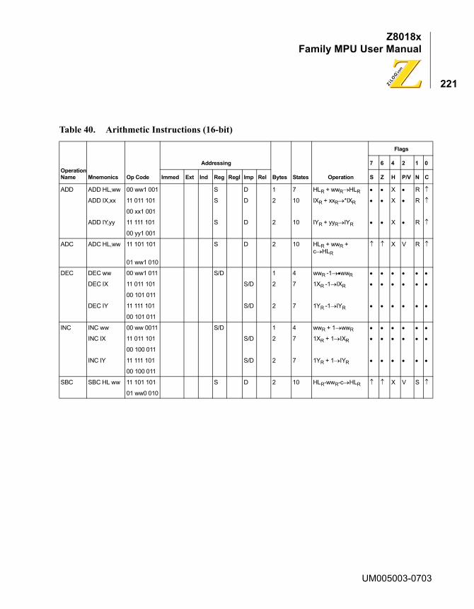
Z8018xFamily MPU User Manual
221
Table 40. Arithmetic Instructions (16-bit)
OperationName Mnemonics Op Code
Addressing
Bytes States Operation
Flags
7 6 4 2 1 0
Immed Ext Ind Reg RegI Imp Rel S Z H P/V N C
ADD ADD HL,ww 00 ww1 001 S D 1 7 HLR + wwR�HLR � � X � R �
ADD IX,xx 11 011 101 S D 2 10 IXR + xxR�*IXR � � X � R �
00 xx1 001
ADD IY,yy 11 111 101 S D 2 10 IYR + yyR�IYR � � X � R �
00 yy1 001
ADC ADC HL,ww 11 101 101 S D 2 10 HLR + wwR + c�HLR
� � X V R �
01 ww1 010
DEC DEC ww 00 ww1 011 S/D 1 4 wwR -1��wwR � � � � � �
DEC IX 11 011 101 S/D 2 7 1XR -1�IXR � � � � � �
00 101 011
DEC IY 11 111 101 S/D 2 7 1YR -1�IYR � � � � � �
00 101 011
INC INC ww 00 ww 0011 S/D 1 4 wwR + 1�wwR � � � � � �
INC IX 11 011 101 S/D 2 7 1XR + 1�IXR � � � � � �
00 100 011
INC IY 11 111 101 S/D 2 7 1YR + 1�IYR � � � � � �
00 100 011
SBC SBC HL ww 11 101 101 S D 2 10 HLR-wwR-c�HLR � � X V S �
01 ww0 010
UM005003-0703

Z8018xFamily MPU User Manual
222
DATA TRANSFER INSTRUCTIONSTable 41. 8-Bit Load
OperationName Mnemonics Op Code
Addressing
Bytes States Operation
Flags
7 6 4 2 1 0
Immed Ext Ind Reg RegI Imp Rel S Z H P/V N C
Load8-BitData
LD A,I 11 101 101 S/D 2 6 1r�Ar � � R IEF2 R �
01 010 111
LD A,R 11 101 101 S/D 2 6 Rr�Ar � � R IEF2 R �
01 011 111
LD A,(BC) 00 001 010 S D 1 6 (BC)M�Ar � � � � � �
LD A,(DE) 00 011 010 S D 1 6 (DE)M�Ar � � � � � �
LD A,(mn) 00 111 010 S D 3 12 (mn)M�Ar � � � � � �
�n�
�m�
LD L,A 11 101 101 S/D 2 6 Ar�Ir � � � � � �
01 000 111
LD R,A 11 101 101 S/D 2 6 Ar�Rr � � � � � �
01 001 111
LD (BC),A 00 000 010 D S 1 7 Ar�(BC)M � � � � � �
LD(DE),A 00 010 010 D S 1 7 Ar��DE)M � � � � � �
LD (mn),A 00 110 010 D S 3 13 Ar�(mn)M � � � � � �
�n�
�m�
LD gg’ 01 g g’ S/D 1 4 gr’�gr � � � � � �
LD g,(HL) 01 g 110 D S 1 6 (HL)M�gr � � � � � �
LD g,m 00 g 110 S D 2 6 m�gr � � � � � �
�m�
LD g,(IX + d) 11 011 101 S D 3 14 (IX + d)Mgr � � � � � �
01 g 110
�d�
LD g,(IY + d) 11 111 101 S D 3 14 (IY + d)M�gr � � � � � �
01 g 110
�d�
LD (HL),m 00 110 110 S D 2 9 m�(HL)M � � � � � �
�m�
UM005003-0703

Z8018xFamily MPU User Manual
223
Load8-BitData
LD (IX + d),m 11 011 101 S D 4 15 m�(IX + d)M � � � � � �
00 110 110
�d�
LD (IY + d),m 11 111 101 S D 4 15 m�(IY + d)M � � � � � �
01 110 g
�d�
<m>
LD (HL),g 01 110 g S D 1 7 gr�(HL)M � � � � � �
LD (IX + d),g 11 011 101 D S 3 15 gr�(IX+d)M � � � � � �
01 110 g
<d>
LD (IY + d),g 11 111 101 D S 3 15 gr�(IY + d)M � � � � � �
01 110 g
�d�
(1) In the case of R1 and Z Mask, interrupts are not sampled at the end of LD A, I or LD A,R.
Table 42. 16-Bit Load
OperationName Mnemonics Op Code
Addressing
Bytes States Operation
Flags
7 6 4 2 1 0
Immed Ext Ind Reg RegI Imp Rel S Z H P/V N C
Load16-Bit Data
LD ww,mn 00 ww0 001 S D 3 9 mn�wwR � � � � � �
�n�
�m�
LD IX,mn 11 011 101 S D 4 12 mn�IXR � � � � � �
00 100 001
�n�
�m�
Table 41. 8-Bit Load (Continued)
OperationName Mnemonics Op Code
Addressing
Bytes States Operation
Flags
7 6 4 2 1 0
Immed Ext Ind Reg RegI Imp Rel S Z H P/V N C
UM005003-0703

Z8018xFamily MPU User Manual
224
Load16-Bit Data
LD IY,mn 11 111 101 S D 4 12 mn�IYR � � � � � �
00 100 001
�n�
�m�
LD SP,HL 11 111 001 S/D 1 4 HIR�SPR � � � � � �
LD SP,IX 11 011 101 S/D 2 7 IXR-SPR � � � � � �
11 111 001
LD SP,IY 11 111 101 S/D 2 7 IYR�SPR � � � � � �
11 111 001
LD ww,(mn) 11 101 101 S D 4 18 (mn + 1)M�wwHr � � � � � �
01 ww1 011 (mn)M�wwLr
�n�
�m�
LD HL,(mn) 00 101 010 S D 3 15 (mn + 1)M�Hr � � � � � �
�n� (mn)M�Lr
�m�
LD IX,(mn) 11 011 101 S D 4 18 (mn + 1)M�IXHr � � � � � �
00 101 010 (mn)M�IXLr
�n�
�m�
LD IY,(mn) 11 111 101 S D 4 18 (mn + 1)M�IYHr � � � � � �
00 101 010 (mn)M��IYLr
�n�
�m�
LD (mn),ww 11 101 101 D S 4 19 wwHr�(mn + 1)M � � � � � �
01 ww0 011 wwLr�(mn)M�n�
�m�
Table 42. 16-Bit Load (Continued)
OperationName Mnemonics Op Code
Addressing
Bytes States Operation
Flags
7 6 4 2 1 0
Immed Ext Ind Reg RegI Imp Rel S Z H P/V N C
UM005003-0703

Z8018xFamily MPU User Manual
225
Load16-bitData
LD (mn),HL 00 100 010 D S 3 16 Hr�(mn + 1)M � � � � � �
�n� Lr�(mn)M�m�
LD (mn),IX 11 011 101 D S 4 19 IXHr-(mn + 1)M � � � � � �
00 100 010 IXLr�(mn)M�n�
�m�
LD (mn),IY 11 111 101 D S 4 19 IYHr�(mn + 1)M � � � � � �
00 100 010 IYLr�(mn)M�n�
�m�
Table 43. Block Transfer
OperationName Mnemonics Op Code
Addressing
Bytes States Operation
Flags
7 6 4 2 1 0
Immed Ext Ind Reg RegI Imp Rel S Z H P/V N C
BlockTransferSearchData
(3) (2)
CPD 11 101 101 S S 2 12 Ar = (HL)M � � � � S �
10 101 001 BCR-1�BCR
HLR-1�HLR (3) (2)
CPDR 11 101 101 S S 2 14 BCR ��0 Ar � (HL)M � � � � S �
10 111 001 12 BCR = 0 or Ar = (HL)MAr-(HL)R
Q BCR-1-BCRHLR-1�HLR
Repeat Q until
Ar = (HL)M or BCR = 0 (3) (2)
Table 42. 16-Bit Load (Continued)
OperationName Mnemonics Op Code
Addressing
Bytes States Operation
Flags
7 6 4 2 1 0
Immed Ext Ind Reg RegI Imp Rel S Z H P/V N C
UM005003-0703

Z8018xFamily MPU User Manual
226
CPI 11101101 S S 2 12 Ar-(HL)M � � � � S �
10100001 BCR-1�BCR
HLR + 1�HLR (3) (2)
CPIR 11101101 S S 2 14 BCR ��0 Ar*(HL)M � � � � S �
10110001 12 BCR = 0 or Ar = (HL)MAr-(HL)M
Q BCR-1�BCRHLR + 1�HLR
Repeat Q until
Ar = (HL)M or BCR = 0 (2)
LDD 11 101 101 S/D 2 12 (HL)M���(DE)M � � R � R �
10 101 000 BCR -1�BCR
DER-1�DER
HLR-1�HLR
LDDR 11 101 101 S/D 2 14(BCR ��0) (HL)M���(DE)MBCR -1 ��BCR
Q DER -1 ��DERHLR -1 ��HLR
� � R R R �
10 111 000 12(BCR �0)
Repeat Q until
BCR = 0 (2)
LDI 11 101 101 S/D 2 12 (HL)M�DE)R � � R � R �
10 100 000 BCR-1�BCR
DER + 1�DER
HLR + 1�HLR
LDIR 11 101 101 S/D 2 14(BCR�0) (HL)M�(DE)MQ BCR-1�BCR
DER + 1�DERHLR + 1�HLR
� � R R R �
10 110 000 12(BCR = 0)
Repeat Q until
BCR = 0
(2) P/V = 0: BCR-1 = 0P/V = 1: BCR-1 ��0
(3) Z = 1: Ar = (HL)MZ = 0 :Ar ���HL)M
Table 43. Block Transfer (Continued)
OperationName Mnemonics Op Code
Addressing
Bytes States Operation
Flags
7 6 4 2 1 0
Immed Ext Ind Reg RegI Imp Rel S Z H P/V N C
UM005003-0703
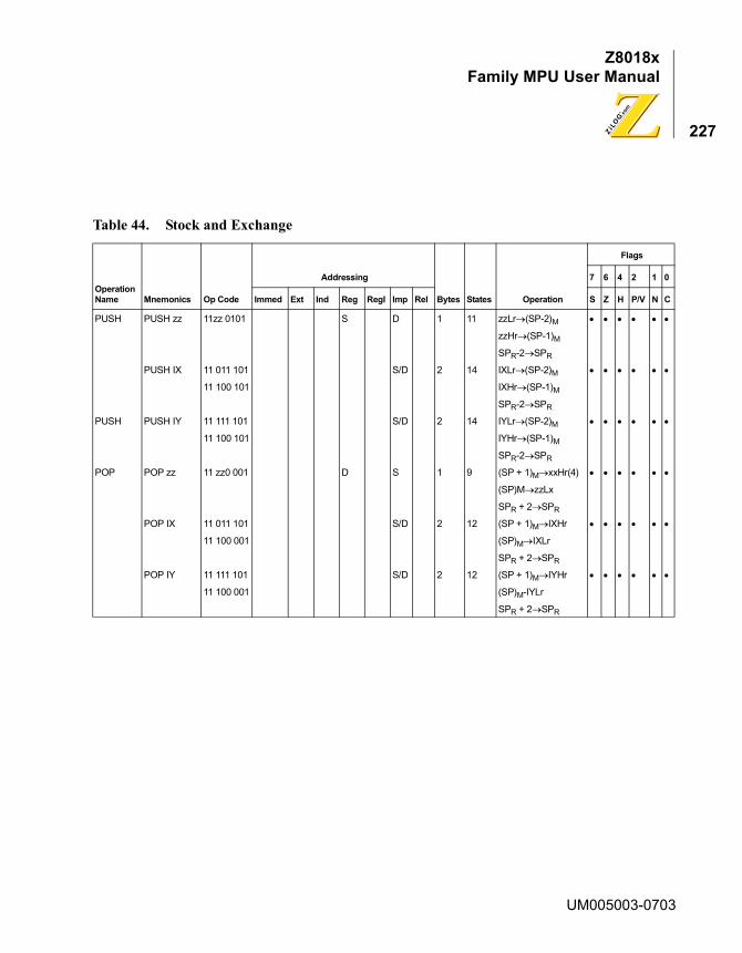
Z8018xFamily MPU User Manual
227
Table 44. Stock and Exchange
OperationName Mnemonics Op Code
Addressing
Bytes States Operation
Flags
7 6 4 2 1 0
Immed Ext Ind Reg RegI Imp Rel S Z H P/V N C
PUSH PUSH zz 11zz 0101 S D 1 11 zzLr�(SP-2)M � � � � � �
zzHr�(SP-1)MSPR-2�SPR
PUSH IX 11 011 101 S/D 2 14 IXLr�(SP-2)M � � � � � �
11 100 101 IXHr�(SP-1)MSPR-2�SPR
PUSH PUSH IY 11 111 101 S/D 2 14 IYLr�(SP-2)M � � � � � �
11 100 101 IYHr�(SP-1)MSPR-2�SPR
POP POP zz 11 zz0 001 D S 1 9 (SP + 1)M�xxHr(4) � � � � � �
(SP)M�zzLx
SPR + 2�SPR
POP IX 11 011 101 S/D 2 12 (SP + 1)M�IXHr � � � � � �
11 100 001 (SP)M�IXLr
SPR + 2�SPR
POP IY 11 111 101 S/D 2 12 (SP + 1)M�IYHr � � � � � �
11 100 001 (SP)M-IYLr
SPR + 2�SPR
UM005003-0703

Z8018xFamily MPU User Manual
228
.
Exchange EX AFAF’ 00 001 000 S/D 1 4 AFR-AFR' � � � � � �
EX DE, HL 11 101 011 S/D 1 3 DER-HLR � � � � � �
EX X 11 011 001 S/D 1 3 BCR-BCR' � � � � � �
DER�DER'
HLR�HLR'
EX (SP),HL 11 100 011 S/D 1 16 Hr�(SP + 1)M � � � � � �
Lr�(SP)MEX (SP),IX 11 011 101 S/D 2 19 IXHr�(SP + 1)M � � � � � �
IXLr-(SP)MEX (SP),IY 11 111 101 S/D 2 19 IYHr-(SP + 1)M � � � � � �
11 100 011 IYLr�(SP)M(4) In the case of POP AF, Flag is written as current contents of the stack
Table 44. Stock and Exchange (Continued)
OperationName Mnemonics Op Code
Addressing
Bytes States Operation
Flags
7 6 4 2 1 0
Immed Ext Ind Reg RegI Imp Rel S Z H P/V N C
UM005003-0703

Z8018xFamily MPU User Manual
229
PROGRAM AND CONTROL INSTRUCTIONS
Table 45. Program Control Instructions
OperationName Mnemonics Op Code
Addressing
Bytes States Operation
Flags
7 6 4 2 1 0
Immed Ext Ind Reg RegI Imp Rel S Z H P/V N C
Call CALL mn 11 001 101 D 3 16 PCHr�(SP-1)M � � � � � �
�n� PCLr�(SP-2)M�m� mn�PCR
SPR-2�SPR
CALL f,mn 11 f 100 D 3 6 (f : false) continue : f is false � � � � � �
�n� 16 (f: true) CALL mn: f is true
�m�
Jump DJNZj 00 010 000 D 2 9 (Br ��0) Br-1�Br � � � � � �
�j-2� 2 7 (Br = 0) continue: Br = 0
PCR + j�PCR: Br ��0
JP f,mn 11 f 010 D 3 6 (f: false) mn�PCR: f is true � � � � � �
�n� 3 9 (f: true) continue: f is false
�m�
JP mn 11 000 011 D 3 9 mn�PCR � � � � � �
�n�
�m�
JP (HL) 11 101 001 D 1 3 HLR�PCR � � � � � �
JP (IX) 11 011 101 D 2 6 IXR�PCR � � � � � �
11 101 001
JP (IY) 11 111 101 D 2 6 IYR�PCR � � � � � �
11 101 001
JR j 00 011 000 D 2 8 PCR + j�PCR � � � � � �
�j-2�
JR Cj 00 111 000 D 2 6 continue: C = 0 � � � � � �
�j-2� 2 8 PCR + j�PCR: C = 1
JR NCj 00 110 000 D 2 6 continue : C = 1 � � � � � �
�j-2� 2 8 PCR + j�PCR : C = 0
UM005003-0703
Z8018xFamily MPU User Manual
230
Jump JR Zj 00 101 000 D 2 6 continue : Z = 0 � � � � � �
�j-2� 2 8 PCR, + j�PCR : Z = 1
JR NZj 00 100 000 D 2 6 continue : Z = 1
�j-2� 2 8 PCR + j�PCR : Z = 0
Return RET 11001001 D 1 9 (SP)M�PCLr � � � � � �
(SP + 1)M�PCHr
SPR + 2�SPR
RET f 11f 000 D 1 5 (f : false) continue : f is false � � � � � �
1 10 (f : true) RET : f is true
RETI 11101101 D 2 12 (R0,R1) (SP)M�PCLr � � � � � �
01001101 ZZ(z) (SP + 1)M�PCHr
SPR + 2�SPR
RETN 11101101 D 2 12 (SP)M�PCLr � � � � � �
01000101 (SP + 1)M�PCHr
SPR + 2�SPR
IEF2�IEF1
Restart RST v 11 v 111 D 1 11 PCHr�(SP-1)M � � � � � �
PCLr�(SP-2)M0�PCHr
v�PCLr
SPR-2�SPR
Table 45. Program Control Instructions (Continued)
OperationName Mnemonics Op Code
Addressing
Bytes States Operation
Flags
7 6 4 2 1 0
Immed Ext Ind Reg RegI Imp Rel S Z H P/V N C
UM005003-0703
Z8018xFamily MPU User Manual
231
Table 46. I/O Instructions
OperationName Mnemonics Op Code
Addressing
Bytes States Operation
Flags
7 6 4 2 1 0
Immed Ext Ind Reg RegI Imp Rel S Z H P/V N C
INPUT IN A,(m) 11 011 011 D S 2 9 (Am)1,�Ar � � � � � �
�m� m�A0~A7
Ar�A8~A16
IN g,(C) 11 101 101 D S 2 9 (BC)1�gr
01 g 000 g = 110 : Only the � � R P R �
flags change
Cr�A0~A7
Br�A8~16
IN0 g,(m)** 11 101 101 D S 3 12 (00m)g�gr � � R P R �
00 g 000 g = 110 : Only the
flags change
�m� m�A0~A7
(00)�A8~A16 (5) (6)
IND 11 101 101 D S 2 12 (BC)M�(HL)M X � X X � X
10 101 010 Hl2�1�Hl2
Br�1�Br
Cr�A0~A7 (6)
INDR 11 101 101 D S 2 14 (Br ��0) (BC)1�(HL)MQ HL2�1�HL8
Br-1�Br
X S X X � X
10 111 010 12 (BR = 0)
Repeat Q until
Br = 0
Cr�A0~A7
Br�A8A16
(5) (6)
INI 11 101 101 D S 2 12 (BC)1�(HL)M X � X X � X
10 100 010 HLR + 1�HLR
Br-1�Br
Cr�A0~A7
Br�A8~A16 (6)
UM005003-0703

Z8018xFamily MPU User Manual
232
INPUT INIR 11 101 101 D S 2 14 (Br ��0) (BC)I�(HL)MQ HLR + 1�HLR
Br-f�Br
X S X X � X
10 110 010 12 (Br = 0)
Repeat Q until
Br = 0
Cr�A0~A7
Br�A8�A16
OUTPUT OUT (m)A 11 010 011 S D 2 10 Ar�(Am)1 � � � � � �
�m� m�A0~A7
Ar�A8~A16
OUT (C),g 11 101 101 S D 2 10 gr�(BC)1 � � � � � �
01 g 001 Cr�A0~A7
Br�A8~A16
OUT0(m),g** 11 101 101 S D 3 13 gr�(00m)1 � � � � � �
00 g 001 m�A0~A7
�m� 00�A8~A16 (5) (6)
OTDM** 11 101 101 S D 2 14 (HL)M�(00C)1 � � � P � �
10 001 011 HLR-1�HLR
Cr-1�Cr
Br-1�Br
Cr�A0~A7
���A8~A16 (6)
OTDMR** 11 101 101 S D 2 16 (Br ��0) (HL)M�(00C)1HLR-1-HLR
Q Cr~1�CrBr-1�Br
R S R S � R
10 011 011 14 (Br = 0)
Repeat Q until
Br = 0
Cr�A0~A7
00�A8~A16 (6)
Table 46. I/O Instructions (Continued)
OperationName Mnemonics Op Code
Addressing
Bytes States Operation
Flags
7 6 4 2 1 0
Immed Ext Ind Reg RegI Imp Rel S Z H P/V N C
UM005003-0703

Z8018xFamily MPU User Manual
233
OUTPUT OTDR 11 101 101 S D 2 14 (Br ��0) (HL)M�(BC)M1Q HLR-1�HLR
Br-1�r
X S X X � X
10 111 011 12 (Br = 0)
Repeat Q until
Br = 0
Cr�A0~A7
Br�A8~A16Q (HL)M�(BC)M
HLR + 1�HLR
(5) (6)
OUTI 11 101 101 S D 2 12 X � X X � X
10 100 011
Br-1�Br
Repeat Q until
BR = 0
Cr�A0~A7
Br�A8~A16 (6)
OTIR 11 101 101 S D 2 14 (Br ��0) (HL)M�(BC)MQ HLR + 1�HLR
Br-1�Br
X S X X � X
10 110 011 12 (Br = 0)
Repeat Q until
Br = 0
Cr�A0~A7
Br�A8~A16
TSTIOm** 11 101 101 S S 3 12 (00C)1*m � � S P R R
01 110 100 Cr�A0~A7
�m� 00�A8~A16 (5) (6)
OTIM** 11 101 101 S D 2 14 (HL)M�(00C)I � � � P � �
10 000 011 HLR + 1�HLR
Cr + 1�Cr
Br-1�Br
Cr�A0~A7
00�A8~A16 (6)
Table 46. I/O Instructions (Continued)
OperationName Mnemonics Op Code
Addressing
Bytes States Operation
Flags
7 6 4 2 1 0
Immed Ext Ind Reg RegI Imp Rel S Z H P/V N C
UM005003-0703
Z8018xFamily MPU User Manual
234
OTIMR** 11 101 101 S D 2 16 (Br ��0) (HL)M�(00C)IHLR + 1�HLR
Q Cr + 1�CrBr-1�Br
R S R S � R
10 010 011 14 (Br = 0)
Repeat Q until
Br = 0
Cr�A0~A7
00�A8~A16 (5) (6)
OUTD 11 101 101 S D 2 12 (HL)M�(BC)1 X � X X � X
10 101 011 HLR-1� LR
Br-1�Br
Cr�A0~A7
Br�A8~A16
(5) Z = 1 : Br-1 = 0Z = 0 : Br-1 ��0
(6) N = 1: MSB of Data = 1N = 0 : MSB of Data = 0
Table 46. I/O Instructions (Continued)
OperationName Mnemonics Op Code
Addressing
Bytes States Operation
Flags
7 6 4 2 1 0
Immed Ext Ind Reg RegI Imp Rel S Z H P/V N C
UM005003-0703
Z8018xFamily MPU User Manual
235
Special Control Instructions
Table 47. Special Control Instructions
OperationName Mnemonics Op Code
Addressing
Bytes States Operation
Flags
7 6 4 2 1 0
Immed Ext Ind Reg Regi Imp Rel S Z H P/V N C
SpecialFunction
DAA 00 100 111 S/D 1 4 DecimalAdjustAccumulator
� � � P � �
CarryControl
CCF 00 111 111 1 3 C�C � � R � R �
SCF 00 110 111 1 3 1�C � � R � R S
CPUControl
DI 11 110 011 1 3 0�IEF1,0�IEF2 (7) � � � � � �
EI 11 111 011 1 3 1�IEF1,1��EF2 (7) � � � � � �
HALT 01 110 110 1 3 CPU halted � � � � � �
IM0 11 101 101 2 6 Interrupt � � � � � �
01 000 110 Mode 0
IM1 11 101 101 2 6 Interrupt � � � � � �
01 010 110 Mode 1
IM2 11 101 101 2 6 Interrupt � � � � � �
01 011 110 Mode 2
NOP 00 000 000 1 3 No operation � � � � � �
SLP** 11 101 101 2 8 Sleep � � � � � �
01 110 110
7) Interrupts are not sampled at the end of DI or EI.
UM005003-0703

Z8018xFamily MPU User Manual
236
UM005003-0703

Z8018xFamily MPU User Manual
237
Instruction Summary** : Added new instructions to Z80
MNEMONICS BytesMachine Cycles States
ADC A,m 2 2 6ADC A,g 1 2 4ADC A, (HL) 1 2 6ADC A, (IX+d) 3 6 14ADC A, (IY+d) 3 6 14ADD A,m 2 2 6ADD A,g 1 2 4ADD A, (HL) 1 2 6ADD A, (IX+d) 3 6 14ADD A, (IY+d) 3 6 14ADC HL,ww 2 6 10ADD HL,ww 1 5 7ADD IX,xx 2 6 10ADD IY,yy 2 6 10AND m 2 2 6AND g 1 2 4AND (HL) 1 2 6AND (IX+d) 3 6 14AND (IY+d) 3 6 14BIT b, HU 2 3 9BIT b, (IX+d) 4 5 15BIT b, (IY+d) 4 5 15BIT b,g 2 2 6CALL f,mn 3 2 6
(If condition is false)
UM005003-0703
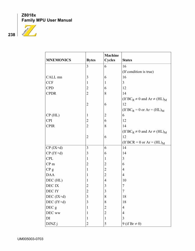
Z8018xFamily MPU User Manual
238
3 6 16(If condition is true)
CALL mn 3 6 16CCF 1 1 3CPD 2 6 12CPDR 2 8 14
(If BCR � 0 and Ar � (HL)M2 6 12
(If BCR = 0 or Ar = (HL)MCP (HL) 1 2 6CPI 2 6 12CPIR 2 8 14
(If BCR � 0 and Ar � (HL)M2 6 12
(If BCR = 0 or Ar = (HL)MCP (IX+d) 3 6 14CP (IY+d) 3 6 14CPL 1 1 3CP m 2 2 6CP g 1 2 4DAA 1 2 4DEC (HL) 1 4 10DEC IX 2 3 7DEC IY 2 3 7DEC (IX+d) 3 8 18DEC (IY+d) 3 8 18DEC g 1 2 4DEC ww 1 2 4DI 1 1 3DJNZ j 2 5 9 (if Br � 0)
MNEMONICS BytesMachine Cycles States
UM005003-0703
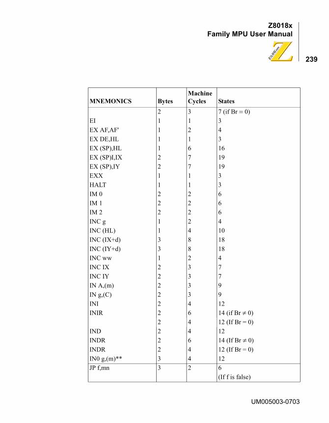
Z8018xFamily MPU User Manual
239
2 3 7 (if Br 0)EI 1 1 3EX AF,AF' 1 2 4EX DE,HL 1 1 3EX (SP),HL 1 6 16EX (SP)I,IX 2 7 19EX (SP),IY 2 7 19EXX 1 1 3HALT 1 1 3IM 0 2 2 6IM 1 2 2 6IM 2 2 2 6INC g 1 2 4INC (HL) 1 4 10INC (IX+d) 3 8 18INC (IY+d) 3 8 18INC ww 1 2 4INC IX 2 3 7INC IY 2 3 7IN A,(m) 2 3 9IN g,(C) 2 3 9INI 2 4 12INIR 2 6 14 (if Br � 0)
2 4 12 (If Br = 0)IND 2 4 12INDR 2 6 14 (If Br � 0)INDR 2 4 12 (If Br = 0)IN0 g,(m)** 3 4 12JP f,mn 3 2 6
(If f is false)
MNEMONICS BytesMachine Cycles States
UM005003-0703
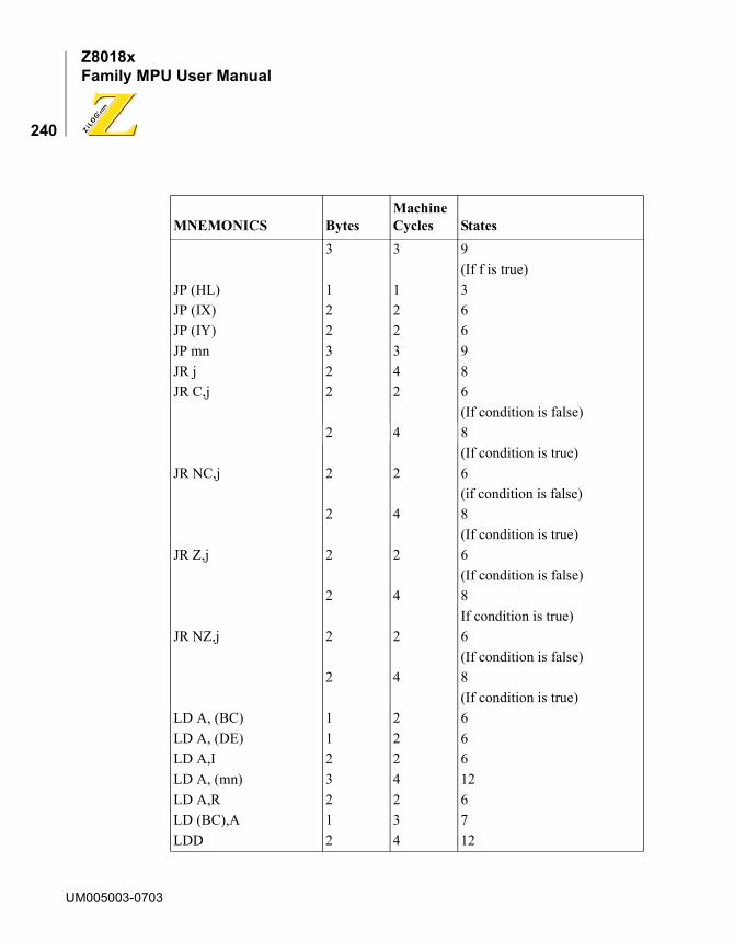
Z8018xFamily MPU User Manual
240
3 3 9(If f is true)
JP (HL) 1 1 3JP (IX) 2 2 6JP (IY) 2 2 6JP mn 3 3 9JR j 2 4 8JR C,j 2 2 6
(If condition is false)2 4 8
(If condition is true)JR NC,j 2 2 6
(if condition is false)2 4 8
(If condition is true)JR Z,j 2 2 6
(If condition is false)2 4 8
If condition is true)JR NZ,j 2 2 6
(If condition is false)2 4 8
(If condition is true)LD A, (BC) 1 2 6LD A, (DE) 1 2 6LD A,I 2 2 6LD A, (mn) 3 4 12LD A,R 2 2 6LD (BC),A 1 3 7LDD 2 4 12
MNEMONICS BytesMachine Cycles States
UM005003-0703

Z8018xFamily MPU User Manual
241
LD (DE),A 1 3 7LD ww,mn 3 3 9LD ww,(mn) 4 6 18LDDR 2 6 14 (If BCR � 0)
2 4 12 (If BCR = 0LD (HL),m 2 3 9LD HL,(mn) 3 5 15LD (HL),g 1 3 7LDI 2 4 12LDI,A 2 2 6LDIR 2 6 14 (If BCR � 0)
2 4 12 (If BCR = 0)LD IX,mn 4 4 12LID IX,(mn) 4 6 18LD (IX+d),m 4 5 15LD (IX+ d),g 3 7 15LD IY,mn 4 4 12LD IY,(mn) 4 6 18LD (IY+d),m 4 5 15LD (IY+d),g 3 7 15LD (mn),A 3 5 13LD (mn),ww 4 7 19LD (mn),HL 3 6 16LD (mn),IX 4 7 19LD (mn),IY 4 7 19LD R,A 2 2 6LD g,(HL) 1 2 6LD g,(IX+d) 3 6 14LD g,(IY+d) 3 6 14LD g,m 2 2 6
MNEMONICS BytesMachine Cycles States
UM005003-0703
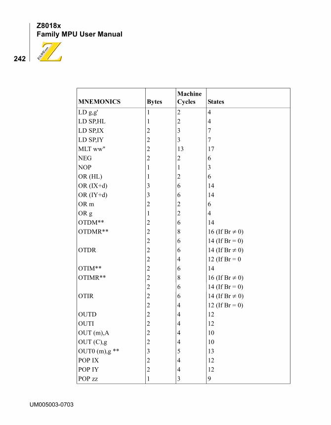
Z8018xFamily MPU User Manual
242
LD g,g' 1 2 4LD SP,HL 1 2 4LD SP,IX 2 3 7LD SP,IY 2 3 7MLT ww" 2 13 17NEG 2 2 6NOP 1 1 3OR (HL) 1 2 6OR (IX+d) 3 6 14OR (IY+d) 3 6 14OR m 2 2 6OR g 1 2 4OTDM** 2 6 14OTDMR** 2 8 16 (If Br � 0)
2 6 14 (If Br = 0)OTDR 2 6 14 (If Br � 0)
2 4 12 (If Br = 0OTIM** 2 6 14OTIMR** 2 8 16 (If Br � 0)
2 6 14 (If Br = 0)OTIR 2 6 14 (If Br ��0)
2 4 12 (If Br = 0)OUTD 2 4 12OUTI 2 4 12OUT (m),A 2 4 10OUT (C),g 2 4 10OUT0 (m),g ** 3 5 13POP IX 2 4 12POP IY 2 4 12POP zz 1 3 9
MNEMONICS BytesMachine Cycles States
UM005003-0703
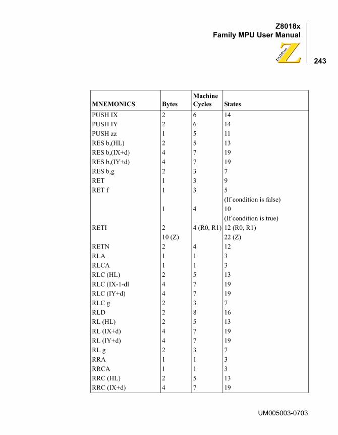
Z8018xFamily MPU User Manual
243
PUSH IX 2 6 14PUSH IY 2 6 14PUSH zz 1 5 11RES b,(HL) 2 5 13RES b,(IX+d) 4 7 19RES b,(IY+d) 4 7 19RES b,g 2 3 7RET 1 3 9RET f 1 3 5
(If condition is false)1 4 10
(If condition is true)RETI 2 4 (R0, R1) 12 (R0, R1)
10 (Z) 22 (Z)RETN 2 4 12RLA 1 1 3RLCA 1 1 3RLC (HL) 2 5 13RLC (IX-1-dl 4 7 19RLC (IY+d) 4 7 19RLC g 2 3 7RLD 2 8 16RL (HL) 2 5 13RL (IX+d) 4 7 19RL (IY+d) 4 7 19RL g 2 3 7RRA 1 1 3RRCA 1 1 3RRC (HL) 2 5 13RRC (IX+d) 4 7 19
MNEMONICS BytesMachine Cycles States
UM005003-0703
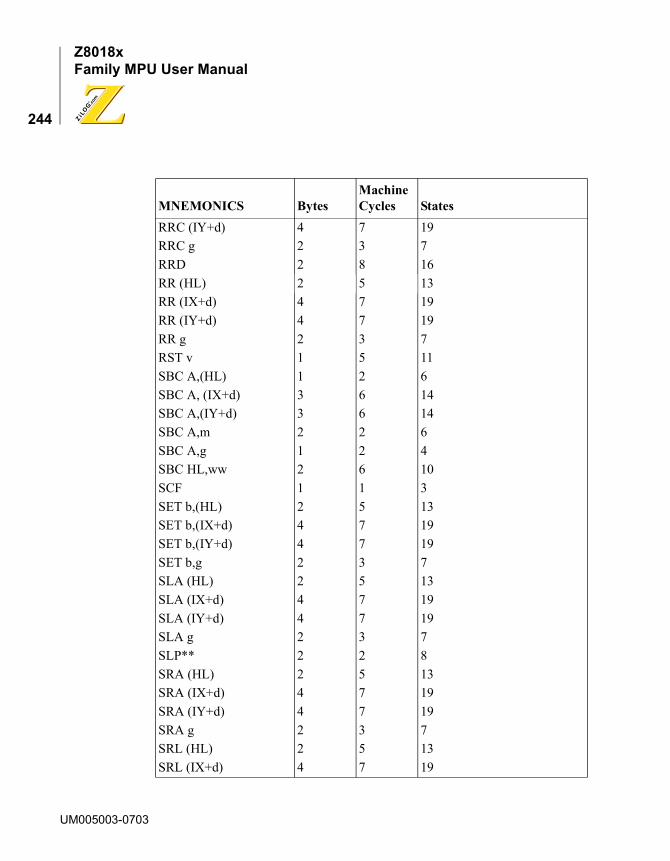
Z8018xFamily MPU User Manual
244
RRC (IY+d) 4 7 19RRC g 2 3 7RRD 2 8 16RR (HL) 2 5 13RR (IX+d) 4 7 19RR (IY+d) 4 7 19RR g 2 3 7RST v 1 5 11SBC A,(HL) 1 2 6SBC A, (IX+d) 3 6 14SBC A,(IY+d) 3 6 14SBC A,m 2 2 6SBC A,g 1 2 4SBC HL,ww 2 6 10SCF 1 1 3SET b,(HL) 2 5 13SET b,(IX+d) 4 7 19SET b,(IY+d) 4 7 19SET b,g 2 3 7SLA (HL) 2 5 13SLA (IX+d) 4 7 19SLA (IY+d) 4 7 19SLA g 2 3 7SLP** 2 2 8SRA (HL) 2 5 13SRA (IX+d) 4 7 19SRA (IY+d) 4 7 19SRA g 2 3 7SRL (HL) 2 5 13SRL (IX+d) 4 7 19
MNEMONICS BytesMachine Cycles States
UM005003-0703
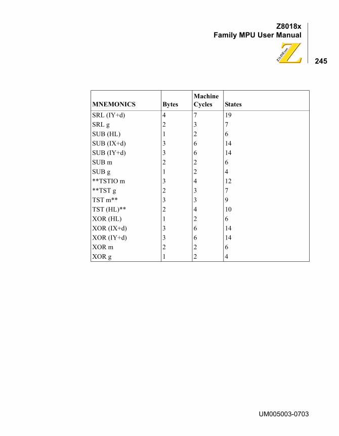
Z8018xFamily MPU User Manual
245
SRL (IY+d) 4 7 19SRL g 2 3 7SUB (HL) 1 2 6SUB (IX+d) 3 6 14SUB (IY+d) 3 6 14SUB m 2 2 6SUB g 1 2 4**TSTIO m 3 4 12**TST g 2 3 7TST m** 3 3 9TST (HL)** 2 4 10XOR (HL) 1 2 6XOR (IX+d) 3 6 14XOR (IY+d) 3 6 14XOR m 2 2 6XOR g 1 2 4
MNEMONICS BytesMachine Cycles States
UM005003-0703

Z8018xFamily MPU User Manual
246
UM005003-0703

Z8018xFamily MPU User Manual
247
Op Code MapTable 48. 1st Op Code Map Instruction Format: XX
ww (L0 = ALL) L0 = 0~7
BC DE HL SP BC DE HL AF zz
g (LO = 0~7) NZ NC P0 P f
B D H (HL) B D H (HL) 00H 10H 20H 30H v
0000 0001 0010 0011 0100 0101 0110 0111 1000 1001 1010 1011 1100 1101 1110 1111
0 1 2 3 4 5 6 7 8 9 A B C D E F
S (H
I = A
LL)
B 0000 0 N0P DJNZj JR NZ,j
JR NC,j
LD g, s
note 1)
ADD A,s
SUB s AND s OR s
RET f 0
C 0001 1 LD ww, mn POP zz 1
D 0010 2 LD (ww), A LD(mn),HL
LD(mn),A
JP f, mn 2
E 0011 3 INC ww JP mn OUT(m),A
EX(SP),HL
DI 3
H 0100 4 INC g note1 CALL f, mn 4
L 0101 5 DEC g note1 PUSH zz 5
(HL) 0110 6 LD g,m note1 note2 HALT note2 note2 note2 note2 ADD A,m
SUB m AND m OR m 6
A 0111 7 RLCA RLA DAA SCF RST v 7
B 1000 8 EXAF,AF’
JR j JR Z,j JR C,j
LD g, s ADC A,s
SBC A,s
XOR s CP s
RET f 8
C 1001 9 ADD HL, ww RET EXX JP(HL) LD SP,HL
9
D 1010 A LD A,(ww) LD HL,(mn)
LD A,(mn)
JP f, mn A
E 1011 B DEC ww Table2 IN A(m) EXDE,HL
EI B
H 1100 C INC g CALL f, mn C
L 1101 D DEC g CALL mn
note3 Table3 note3 D
(HL) 1110 E LD g,m note2 note2 note2 note2 note2 ADC A,m
SBC A,m XOR m CP m E
A 1111 F RRCA RRA CPL CCF RST v F
0 1 2 3 4 5 6 7 8 9 A B C D E F
C E L A C E L A Z C PE M f
g(L0 = 8~F) 08H 18H 28H 3BH v
LO = 8~F
LOHI
UM005003-0703

Z8018xFamily MPU User Manual
248
Note 1: (HL) replaces g.
Note 2: (HL) replaces s.
Note 3: If DDH is supplemented as first Op Code for the instructions which have HL or (HL) as an operand in Table 48, the instructions are executed replacing HL with IX and (HL) with (IX+d).
ex. 22H : LD (mn), HL
DDH 22H : LD (mn), IX
If FDH is supplemented as 1st Op Code for the instructions which have HL or (HL) as an operand in Table 48, the instructions are executed replacing HL with IY and (HL) with (IY+d).
ex. 34H : INC (HL)
FDH 34H : INC (IY+d)
However, JP (HL) and EX DE, HL are exceptions and note the following.
• If DDH is supplemented as 1st Op Code for JP (HL), (IX) replaces (HL) as operand and JP (IX) is executed
• If FDH is supplemented as 1st Op Code for JP (HL), (IY) replaces (HL) as operand and JP (IY) is executed
• Even if DDH or FDH is supplemented as 1st Op Code for EX DE, HL, HL is not replaced and the instruction is regarded as illegal instruction.
UM005003-0703

Z8018xFamily MPU User Manual
249
Table 49. 2nd Op Code Map Instruction Format: CB XX
b (L0 = 0~7)
0 2 4 6 0 2 4 6 0 2 4 6
0000 0001 0010 0011 0100 0101 0110 0111 1000 1001 1010 1011 1100 1101 1110 1111
0 1 2 3 4 5 6 7 8 9 A B C D E F
g (H
I = A
LL)
B 0000 0
RLC g RL g SLA g
BIT b,g RES b,g SET b,g
0
C 0001 1 1
D 0010 2 2
E 0011 3 3
H 0100 4 4
L 0101 5 5
(HL)
0110 6 NOTE1)
NOTE1)
NOTE1)
NOTE1) NOTE1) NOTE1) 6
A 0111 7 7
B 1000 8
BIT b,g RES b,g SET b,g
8
C 1001 9 RRC g RR g SRA g SRL g 9
D 1010 A A
E 1011 B B
H 1100 C C
L 1101 D D
(HL)
1110 E NOTE1)
NOTE1)
NOTE1)
NOTE1)
NOTE1) NOTE1) NOTE 1) E
A 1111 F F
0 1 2 3 4 5 6 7 8 9 A B C D E F
1 3 5 7 1 3 5 7 1 3 5 7
b (LO = 8 ~ F)
LOHI
UM005003-0703

Z8018xFamily MPU User Manual
250
Table 50. 2nd Op Code Map Instruction Format: ED XX
ww (L0 = ALL)
BC DE HL SP
G (L0 = 0~7)
B D H B D H
0000 0001 0010 0011 0100 0101 0110 0111 1000 1001 1010 1011 1100 1101 1110 1111
0 1 2 3 4 5 6 7 8 9 A B C D E F
0000 0 IN0 g, (m) IN g, (C) LDI LDIR 0
0001 1 OUT0 (m),g OUT (C),g CPI CPIR 1
0010 2 SBC HL, ww INI INIR 2
0011 3 LD (mn), ww OTIM OTIMR
OUTI OTIR 3
0100 4 TST g TST (HL)
NEG TST m TSTIO m
4
0101 5 RETN 5
0110 6 IM 0 IM 1 SLP 6
0111 7 LD I,A LD A,I RRD 7
1000 8 IN0 g, (m) IN g, (C) LDD LDDR 8
1001 9 OUT0 (m), g OUT (C) , g CPD CPDR 9
1010 A ADC HL,ww IND INDR A
1011 B LD ww, (mn) OTDM
OTDMR
OUTD OTDR B
1100 C TST g MLT ww C
1101 D RETI D
1110 E IM 2 E
1111 F LDR,A
LD A,R RLD F
0 1 2 3 4 5 6 7 8 9 A B C D E F
C E L A C E L A
g (L0 = 8~F)
LOHI
UM005003-0703

Z8018xFamily MPU User Manual
251
Bus Control Signal Conditions
BUS AND CONTROL SIGNAL CONDITION IN EACH MACHINE CYCLE
* (ADDRESS) invalid
Z (DATA) high impedance.
** added new instructions to Z80
Table 51. Bus and Control Signal Condition in Each Machine Cycle
InstructionMachine Cycle States Address Data RD WR MREQ IORQ M1 HALT ST
ADD HL,ww
MC1 T1T2T3 1st Op Code Address
1st Op Code
0 1 0 1 0 1 0
MC2 ~MC5
TiTiTiTi * Z 1 1 1 1 1 1 1
ADD IX,xxADD IY,yy
MC1 T1T2T3 1st Op Code Address
1st Op Code
0 1 0 1 0 1 0
MC2 T1T2T3 2nd Op Code Address
2nd Op Code
0 1 0 1 0 1 1
MC3 ~MC6
TiTiTiTi * Z 1 1 1 1 1 1 1
ADC HL,wwSBC HL,ww
MC1 T1T2T3 1st Op Code Address
1st Op Code
0 1 0 1 0 1 0
MC2 T1T2T3 2nd Op Code Address
2nd Op Code
0 1 0 1 0 1 1
MC3 ~MC6
TiTiTiTi * Z 1 1 1 1 1 1 1
UM005003-0703

Z8018xFamily MPU User Manual
252
ADD A,g ADC A,gSUB g SBC A,gAND gOR gXOR gCP g
MC1 T1T2T3 1st Op Code Address
1st Op Code
0 1 0 1 0 1 0
MC2 Ti * Z 1 1 1 1 1 1 1
ADD A,mADC A,mSUB mSBC A,mAND mOR mXOR mCP m
MC1 T1T2T3 1st Op Code Address
1st Op Code
0 1 0 1 0 1 0
MC2 T1T2T3 1st operand Address
m 0 1 0 1 1 1 1
ADD A, (HL)ADC A, (HL)SUB (HL)SBC A, (HL)AND HUOR (HL)XOR (HL)CP (HL)
MC1 T1T2T3 1st Op Code Address
1st Op Code
0 1 0 1 0 1 0
MC2 T1T2T3 HL DATA 0 1 0 1 1 1 1
ADD A, (IX+ d)ADD A, (IY+d)ADC A, (IX+d)ADC A, (IY+d)SUB (lX+d)SUB (IY+d)SBC A, (IX+ d)
MC1 T1T2T3 1st Op Code Address
1st Op Code
0 1 0 1 0 1 0
MC2 T1T2T3 2nd Op Code Address
2nd Op Code
0 1 0 1 0 1 1
SBC A, (IY+ d)AND (IX+d)
MC3 T1T2T3 1st operand Address
d 0 1 0 1 1 1 1
Table 51. Bus and Control Signal Condition in Each Machine Cycle (Continued)
InstructionMachine Cycle States Address Data RD WR MREQ IORQ M1 HALT ST
UM005003-0703
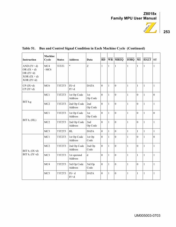
Z8018xFamily MPU User Manual
253
AND (IY+ d)OR (IX + d)OR (IY+d)XOR (IX + d)XOR (IY+d)
MC4~MC6
TiTiTi * Z 1 1 1 1 1 1 1
CP (IX+d)CP (IY+d)
MC6 T1T2T3 IX+dIY+d
DATA 0 1 0 1 1 1 1
BIT b,g
MC1 T1T2T3 1st Op Code Address
1stOp Code
0 1 0 1 0 1 0
MC2 T1T2T3 2nd Op Code Address
2ndOp Code
0 1 0 1 0 1 1
BIT b, (HL)
MC1 T1T2T3 1st Op Code Address
1stOp Code
0 1 0 1 0 1 0
MC2 T1T2T3 2nd Op Code Address
2ndOp Code
0 1 0 1 0 1 1
MC3 T1T2T3 HL DATA 0 1 0 1 1 1 1
BIT b, (IX+d)BIT b, (IY+d)
MC1 T1T2T3 1st Op Code Address
1st Op Code
0 1 0 1 0 1 0
MC2 T1T2T3 2nd Op Code Address
2nd Op Code
0 1 0 1 0 1 1
MC3 T1T2T3 1st operand Address
d 0 1 0 1 1 1 1
MC4 T1T2T3 3rd Op Code Address
3rd Op Code
0 1 0 1 0 1 1
MC5 T1T2T3 IX+ dIY+d
DATA 0 1 0 1 1 1 1
Table 51. Bus and Control Signal Condition in Each Machine Cycle (Continued)
InstructionMachine Cycle States Address Data RD WR MREQ IORQ M1 HALT ST
UM005003-0703

Z8018xFamily MPU User Manual
254
CALL mn
MC1 T1T2T3 1st Op Code Address
1st Op Code
0 1 0 1 0 1 0
MC2 T1T2T3 1st operand Address
n 0 1 0 1 1 1 1
MC3 T1T2T3 2nd operand Address
m 0 1 0 1 1 1 1
MC4 Ti * Z 1 1 1 1 1 1 1
MC5 T1T2T3 SP-1 PCH 1 0 0 1 1 1 1
MC6 T1T2T3 SP-2 PCL 1 0 0 1 1 1 1
CALL f,mn (If condition is false)
MC1 T1T2T3 1st Op Code Address
1st Op Code
0 1 0 1 0 1 0
MC2 T1T2T3 1st operand Address
n 0 1 0 1 1 1 1
CALL f,mnif condition is true)
MC1 T1T2T3 1st Op Code Address
1st Op Code
0 1 0 1 0 1 0
MC2 T1T2T3 1st operand Address
n 0 1 0 1 1 1 1
MC3 T1T2T3 2nd operand Address
m 0 1 0 1 1 1 1
MC4 Ti * Z 1 1 1 1 1 1 1
MC5 T1T2T3 SP-1 PCH 1 0 0 1 1 1 1
MC6 T1T2T3 SP-2 PCL 1 0 0 1 1 1 1
CCF MC1 T1T2T3 1st Op Code Address
1st Op Code
0 1 0 1 0 1 0
Table 51. Bus and Control Signal Condition in Each Machine Cycle (Continued)
InstructionMachine Cycle States Address Data RD WR MREQ IORQ M1 HALT ST
UM005003-0703

Z8018xFamily MPU User Manual
255
CPICPD
MC1 T1T2T3 1st Op Code Address
1st Op Code
0 1 0 1 0 1 0
MC2 T1T2T3 2nd Op Code Address
2nd Op Code
0 1 0 1 0 1 1
MC3 T1T2T3 HL DATA 0 1 0 1 1 1 1
MC4 ~MC6
TiTiTi * Z 1 1 1 1 1 1 1
CPIRCPDR(If BCR ��0 andAr = (HL)M)
MC1 T1T2T3 1st Op Code Address
1st Op Code
0 1 0 1 0 1 0
MC2 T1T2T3 2nd Op Code Address
2nd Op Code
0 1 0 1 0 1 1
MC3 T1T2T3 HL DATA 0 1 0 1 1 1 1
MC4~MC8
TiTiTiTiTi
* Z 1 1 1 1 1 1 1
CPIRCPDR(If BCR=0 orAr=(HL)M)
MC1 T1T2T3 1st Op Code Address
1st Op Code
0 1 0 1 0 1 0
MC2 T1T2T3 2nd Op Code Address
2nd Op Code
0 1 0 1 0 1 1
MC3 T1T2T3 HL DATA 0 1 0 1 1 1 1
MC4~MC6
TiTiTi * Z 1 1 1 1 1 1 1
CPL MC1 T1T2T3 1st Op Code Address
1st Op Code
0 1 0 1 0 1 0
DAAMC1 T1T2T3 1st Op Code
Address1st Op Code
0 1 0 1 0 1 0
MC2 Ti * Z 1 1 1 1 1 1 1
DI*1 MC1 T1T2T3 1st Op Code Address
1st Op Code
0 1 0 1 0 1 0
* 1 Interrupt request is not sampled.
Table 51. Bus and Control Signal Condition in Each Machine Cycle (Continued)
InstructionMachine Cycle States Address Data RD WR MREQ IORQ M1 HALT ST
UM005003-0703
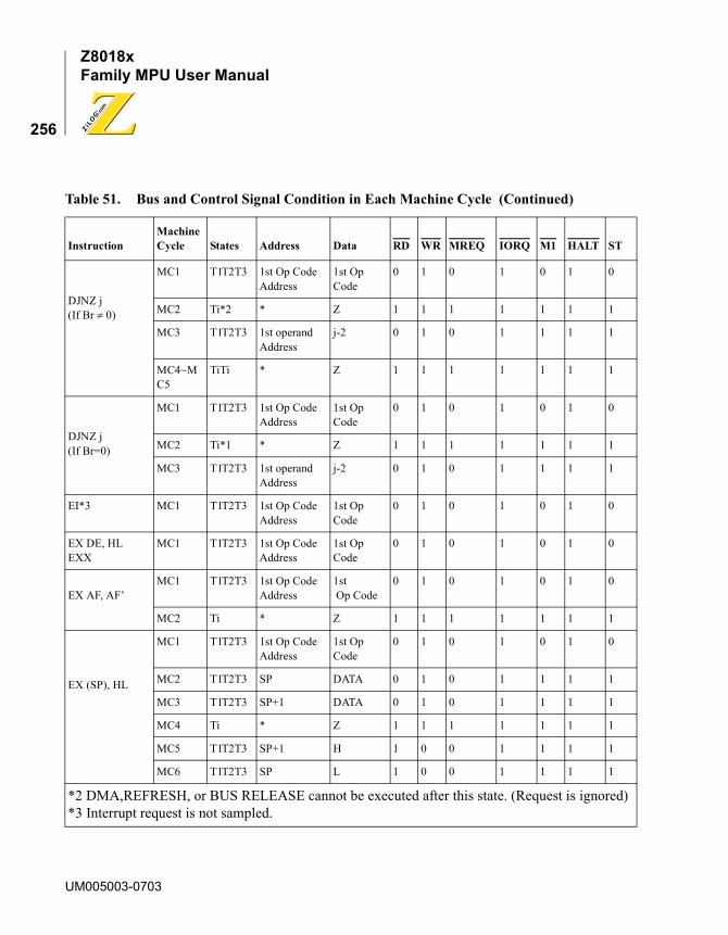
Z8018xFamily MPU User Manual
256
DJNZ j(If Br � 0)
MC1 T1T2T3 1st Op Code Address
1st Op Code
0 1 0 1 0 1 0
MC2 Ti*2 * Z 1 1 1 1 1 1 1
MC3 T1T2T3 1st operand Address
j-2 0 1 0 1 1 1 1
MC4~MC5
TiTi * Z 1 1 1 1 1 1 1
DJNZ j(If Br=0)
MC1 T1T2T3 1st Op Code Address
1st Op Code
0 1 0 1 0 1 0
MC2 Ti*1 * Z 1 1 1 1 1 1 1
MC3 T1T2T3 1st operand Address
j-2 0 1 0 1 1 1 1
EI*3 MC1 T1T2T3 1st Op Code Address
1st Op Code
0 1 0 1 0 1 0
EX DE, HLEXX
MC1 T1T2T3 1st Op Code Address
1st Op Code
0 1 0 1 0 1 0
EX AF, AF’MC1 T1T2T3 1st Op Code
Address1st Op Code
0 1 0 1 0 1 0
MC2 Ti * Z 1 1 1 1 1 1 1
EX (SP), HL
MC1 T1T2T3 1st Op Code Address
1st Op Code
0 1 0 1 0 1 0
MC2 T1T2T3 SP DATA 0 1 0 1 1 1 1
MC3 T1T2T3 SP+1 DATA 0 1 0 1 1 1 1
MC4 Ti * Z 1 1 1 1 1 1 1
MC5 T1T2T3 SP+1 H 1 0 0 1 1 1 1
MC6 T1T2T3 SP L 1 0 0 1 1 1 1
*2 DMA,REFRESH, or BUS RELEASE cannot be executed after this state. (Request is ignored)*3 Interrupt request is not sampled.
Table 51. Bus and Control Signal Condition in Each Machine Cycle (Continued)
InstructionMachine Cycle States Address Data RD WR MREQ IORQ M1 HALT ST
UM005003-0703
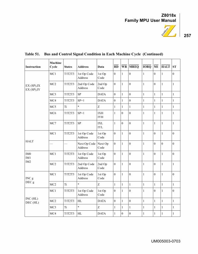
Z8018xFamily MPU User Manual
257
EX (SP),IXEX (SP),IY
MC1 T1T2T3 1st Op Code Address
1st Op Code
0 1 0 1 0 1 0
MC2 T1T2T3 2nd Op Code Address
2nd Op Code
0 1 0 1 0 1 1
MC3 T1T2T3 SP DATA 0 1 0 1 1 1 1
MC4 T1T2T3 SP+1 DATA 0 1 0 1 1 1 1
MC5 Ti * Z 1 1 1 1 1 1 1
MC6 T1T2T3 SP+1 IXHIYH
1 0 0 1 1 1 1
MC7 T1T2T3 SP IXLIYL
1 0 0 1 1 1 1
HALT
MC1 T1T2T3 1st Op Code Address
1st Op Code
0 1 0 1 0 1 0
— — Next Op Code Address
Next Op Code
0 1 0 1 0 0 0
IM0IM1IM2
MC1 T1T2T3 1st Op Code Address
1st Op Code
0 1 0 1 0 1 0
MC2 T1T2T3 2nd Op Code Address
2nd Op Code
0 1 0 1 0 1 1
INC gDEC g
MC1 T1T2T3 1st Op Code Address
1st Op Code
0 1 0 1 0 1 0
MC2 Ti * Z 1 1 1 1 1 1 1
INC (HL)DEC (HL)
MC1 T1T2T3 1st Op Code Address
1st Op Code
0 1 0 1 0 1 0
MC2 T1T2T3 HL DATA 0 1 0 1 1 1 1
MC3 Ti * Z 1 1 1 1 1 1 1
MC4 T1T2T3 HL DATA 1 0 0 1 1 1 1
Table 51. Bus and Control Signal Condition in Each Machine Cycle (Continued)
InstructionMachine Cycle States Address Data RD WR MREQ IORQ M1 HALT ST
UM005003-0703
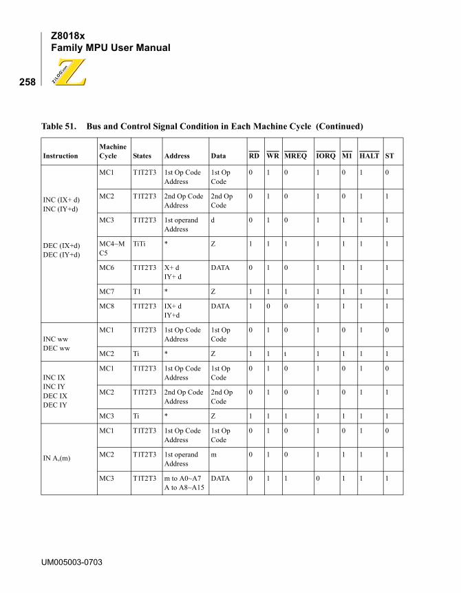
Z8018xFamily MPU User Manual
258
INC (IX+ d)INC (IY+d)
DEC (IX+d)DEC (IY+d)
MC1 T1T2T3 1st Op Code Address
1st Op Code
0 1 0 1 0 1 0
MC2 T1T2T3 2nd Op Code Address
2nd Op Code
0 1 0 1 0 1 1
MC3 T1T2T3 1st operand Address
d 0 1 0 1 1 1 1
MC4~MC5
TiTi * Z 1 1 1 1 1 1 1
MC6 T1T2T3 X+ dIY+ d
DATA 0 1 0 1 1 1 1
MC7 T1 * Z 1 1 1 1 1 1 1
MC8 T1T2T3 IX+ dIY+d
DATA 1 0 0 1 1 1 1
INC wwDEC ww
MC1 T1T2T3 1st Op Code Address
1st Op Code
0 1 0 1 0 1 0
MC2 Ti * Z 1 1 t 1 1 1 1
INC IXINC IYDEC IXDEC IY
MC1 T1T2T3 1st Op Code Address
1st Op Code
0 1 0 1 0 1 0
MC2 T1T2T3 2nd Op Code Address
2nd Op Code
0 1 0 1 0 1 1
MC3 Ti * Z 1 1 1 1 1 1 1
IN A,(m)
MC1 T1T2T3 1st Op Code Address
1st Op Code
0 1 0 1 0 1 0
MC2 T1T2T3 1st operand Address
m 0 1 0 1 1 1 1
MC3 T1T2T3 m to A0~A7A to A8~A15
DATA 0 1 1 0 1 1 1
Table 51. Bus and Control Signal Condition in Each Machine Cycle (Continued)
InstructionMachine Cycle States Address Data RD WR MREQ IORQ M1 HALT ST
UM005003-0703

Z8018xFamily MPU User Manual
259
IN g,(C)
MC1 T1T2T3 1st Op Code Address
1st Op Code
0 1 0 1 0 1 0
MC2 T1T2T3 2nd Op Code Address
2nd Op Code
0 1 0 1 0 1 1
MC3 T1T2T3 BC DATA 0 1 1 0 1 1 1
INO g,(m)**
MC1 T1T2T3 1st Op Code Address
1st Op Code
0 1 0 1 0 1 0
MC2 T1T2T3 2nd Op Code Address
2nd Op Code
0 1 0 1 0 1 1
MC3 T1T2T3 1st operand Address
m 0 1 0 1 1 1 1
MC4 T1T2T3 m to A0~A700H to A8~A15
DATA 0 1 1 0 1 1 1
INIIND
MC1 T1T2T3 1st Op Code Address
1st Op Code
0 1 0 1 0 1 0
MC2 T1T2T3 2nd Op Code Address
2nd Op Code
0 1 0 1 0 1 1
MC3 T1T2T3 BC DATA 0 1 1 0 1 1 1
MC4 T1T2T3 HL DATA 1 0 0 1 1 1 1
INIRINDR(If Br�0)
MC1 T1T2T3 1st Op Code Address
1st Op Code
0 1 0 1 0 1 0
MC2 T1T2T3 2nd Op Code Address
2nd Op Code
0 1 0 1 0 1 1
MC3 T1T2T3 BC DATA 0 1 1 0 1 1 1
MC4 T1T2T3 HL DATA 1 0 0 1 1 1 1
MC5~MC6
TiTi * Z 1 1 1 1 1 1 1
Table 51. Bus and Control Signal Condition in Each Machine Cycle (Continued)
InstructionMachine Cycle States Address Data RD WR MREQ IORQ M1 HALT ST
UM005003-0703
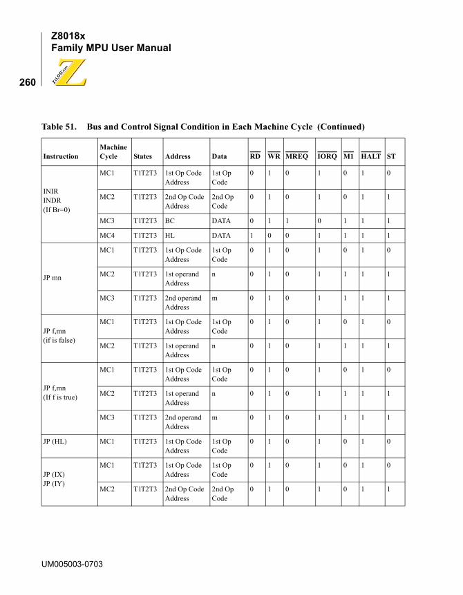
Z8018xFamily MPU User Manual
260
INIRINDR(If Br=0)
MC1 T1T2T3 1st Op Code Address
1st Op Code
0 1 0 1 0 1 0
MC2 T1T2T3 2nd Op Code Address
2nd Op Code
0 1 0 1 0 1 1
MC3 T1T2T3 BC DATA 0 1 1 0 1 1 1
MC4 T1T2T3 HL DATA 1 0 0 1 1 1 1
JP mn
MC1 T1T2T3 1st Op Code Address
1st Op Code
0 1 0 1 0 1 0
MC2 T1T2T3 1st operand Address
n 0 1 0 1 1 1 1
MC3 T1T2T3 2nd operand Address
m 0 1 0 1 1 1 1
JP f,mn(if is false)
MC1 T1T2T3 1st Op Code Address
1st Op Code
0 1 0 1 0 1 0
MC2 T1T2T3 1st operand Address
n 0 1 0 1 1 1 1
JP f,mn(If f is true)
MC1 T1T2T3 1st Op Code Address
1st Op Code
0 1 0 1 0 1 0
MC2 T1T2T3 1st operand Address
n 0 1 0 1 1 1 1
MC3 T1T2T3 2nd operand Address
m 0 1 0 1 1 1 1
JP (HL) MC1 T1T2T3 1st Op Code Address
1st Op Code
0 1 0 1 0 1 0
JP (IX)JP (IY)
MC1 T1T2T3 1st Op Code Address
1st Op Code
0 1 0 1 0 1 0
MC2 T1T2T3 2nd Op Code Address
2nd Op Code
0 1 0 1 0 1 1
Table 51. Bus and Control Signal Condition in Each Machine Cycle (Continued)
InstructionMachine Cycle States Address Data RD WR MREQ IORQ M1 HALT ST
UM005003-0703

Z8018xFamily MPU User Manual
261
JR j
MC1 T1T2T3 1st Op Code Address
1st Op Code
0 1 0 1 0 1 0
MC2 T1T2T3 1st operand Address
j-2 0 1 0 1 1 1 1
MC3~MC4
TiTi * Z 1 1 1 1 1 1 1
JR C,j JR NC,jJR Z,j JR NZ,j(if conditionis false)
MC1 T1T2T3 1st Op Code Address
1st Op Code
0 1 0 1 0 1 0
MC2 T1T2T3 1st operand Address
j-2 0 1 0 1 1 1 1
JR C,j JR NC,jJR Z,j JR NZ,j(if conditionis true)
MC1 T1T2T3 1st Op Code Address
1st Op Code
0 1 0 1 0 1 0
MC2 T1T2T3 1st operand Address
j-2 0 1 0 1 1 1 1
MC3~MC4
TiTi * Z 1 1 1 1 1 1 1
LD g,g'MC1 T1T2T3 1st Op Code
Address1st Op Code
0 1 0 1 0 1 0
MC2 Ti * Z 1 1 1 1 1 1 1
LD g,m
MC1 T1T2T3 1st Op Code Address
1st Op Code
0 1 0 1 0 1 0
MC2 T1T2T3 1st operand Address
m 0 1 0 1 1 1 1
LD g, (HL)MC1 T1T2T3 1st Op Code
Address1st Op Code
0 1 0 1 0 1 0
MC2 T1T2T3 HL DATA 0 1 0 1 1 1 1
Table 51. Bus and Control Signal Condition in Each Machine Cycle (Continued)
InstructionMachine Cycle States Address Data RD WR MREQ IORQ M1 HALT ST
UM005003-0703

Z8018xFamily MPU User Manual
262
LD g, (IX+d)LD g, (IY+d)
MC1 T1T2T3 1st Op Code Address
1st Op Code
0 1 0 1 0 1 0
MC2 T1T2T3 2nd Op Code Address
2nd Op Code
0 1 0 1 0 1 1
MC3 T1T2T3 1st operand Address
d 0 1 0 1 1 1 1
MC4~MC5
TiTi * Z 1 1 1 1 1 1 1
MC6 T1T2T3 IX+dIY+d
DATA 0 1 0 1 1 1 1
LD (HL),g
MC1 T1T2T3 1st Op Code Address
1st Op Code
0 1 0 1 0 1 0
MC2 Ti * Z 1 1 1 1 1 1 1
MC3 T1T2T3 HL g 1 0 0 1 1 1 1
LD (IX + d),gLD (IY + d),g
MC1 T1T2T3 1st Op Code Address
1st Op Code
0 1 0 1 0 1 0
MC2 T1T2T3 2nd Op Code Address
2nd Op Code
0 1 0 1 0 1 1
MC3 T1T2T3 1st operand Address
d 0 1 0 1 1 1 1
MC4~MC6
TiTiTi * Z 1 1 1 1 1 1 1
MC7 T1T2T3 IX+dIY+d
g 1 0 0 1 1 1 1
LD (HL),m
MC1 T1T2T3 1st Op Code Address
1st Op Code
0 1 0 1 0 1 0
MC2 T1T2T3 1st operand Address
m 0 1 0 1 1 1 1
MC3 T1T2T3 HL DATA 1 0 0 1 1 1 1
Table 51. Bus and Control Signal Condition in Each Machine Cycle (Continued)
InstructionMachine Cycle States Address Data RD WR MREQ IORQ M1 HALT ST
UM005003-0703

Z8018xFamily MPU User Manual
263
LD (IX+d),mLD (IY+d),m
MC1 T1T2T3 1st Op Code Address
1st Op Code
0 1 0 1 0 1 0
MC2 T1T2T3 2nd Op Code Address
2nd Op Code
0 1 0 1 0 1 1
MC3 T1T2T3 1st operand Address
d 0 1 0 1 1 1 1
MC4 T1T2T3 2nd operand Address
m 0 1 0 1 1 1 1
MC5 T1T2T3 IX+ dIY+d
DATA 1 0 0 1 1 1 1
LD A, (BC)LD A, (DE)
MC1 T1T2T3 1st Op Code Address
1st Op Code
0 1 0 1 0 1 0
MC2 T1T2T3 BCDE
DATA 0 1 0 1 1 1 1
LD A,(mn)
MC1 T1T2T3 1st Op Code Address
1st Op Code
0 1 0 1 0 1 0
MC2 T1T2T3 1st operand Address
n 0 1 0 1 1 1 1
MC3 T1T2T3 2nd operand Address
m 0 1 0 1 1 1 1
MC4 T1T2T3 mn DATA 0 1 0 1 1 1 1
LD (BC),ALD (DE),A
MC1 T1T2T3 1st Op Code Address
1st Op Code
0 1 0 1 0 1 0
MC2 Ti * Z 1 1 1 1 1 1 1
MC3 T1T2T3 BCDE
A 1 0 0 1 1 1 1
Table 51. Bus and Control Signal Condition in Each Machine Cycle (Continued)
InstructionMachine Cycle States Address Data RD WR MREQ IORQ M1 HALT ST
UM005003-0703

Z8018xFamily MPU User Manual
264
LD (mn),A
MC1 T1T2T3 1st Op Code Address
1st Op Code
0 1 0 1 0 1 0
MC2 T1T2T3 1st operand Address
n 0 1 0 1 1 1 1
MC3 T1T2T3 2nd operand Address
m 0 1 0 1 1 1 1
MC4 Ti * Z 1 1 1 1 1 1 1
MC5 T1T2T3 mn A 1 0 0 1 1 1 1
LD A,ILD A,RLD I,ALD R,A
MC1 T1T2T3 1st Op Code Address
1st Op Code
0 1 0 1 0 1 0
MC2 T1T2T3 2nd Op Code Address
2nd Op Code
0 1 0 1 0 1 1
LD ww, mn
MC1 T1T2T3 1st Op Code Address
1st Op Code
0 1 0 1 0 1 0
MC2 T1T2T3 1st operand Address
n 0 1 0 1 1 1 1
MC3 T1T2T3 2nd operand Address
m 0 1 0 1 1 1 1
LD IX,mnLD IY,mn
MC1 T1T2T3 1st Op Code Address
1st Op Code
0 1 0 1 0 1 0
MC2 T1T2T3 2nd Op Code Address
2nd Op Code
0 1 0 1 0 1 1
MC3 T1T2T3 1st operand Address
n 0 1 0 1 1 1 1
MC4 T1T2T3 2nd operand Address
m 0 1 0 1 1 1 1
*4 In the case of R1 and Z MASK, interrupt request is not sampled.
Table 51. Bus and Control Signal Condition in Each Machine Cycle (Continued)
InstructionMachine Cycle States Address Data RD WR MREQ IORQ M1 HALT ST
*4
UM005003-0703
Z8018xFamily MPU User Manual
265
LD HL, (mn)
MC1 T1T2T3 1st Op Code Address
1st Op Code
0 1 0 1 0 1 0
MC2 T1T2T3 1st operand Address
n 0 1 0 1 1 1 1
MC3 T1T2T3 2nd operand Address
m 0 1 0 1 1 1 1
MC4 T1T2T3 mn DATA 0 1 0 1 1 1 1
MC5 T1T2T3 mn+1 DATA 0 1 0 1 1 1 1
LD ww,(mn)
MC1 T1T2T3 1st Op Code Address
1st Op Code
0 1 0 1 0 1 0
MC2 T1T2T3 2nd Op Code Address
2nd Op Code
0 1 0 1 0 1 1
MC3 T1T2T3 1st operand Address
n 0 1 0 1 1 1 1
MC4 T1T2T3 2nd operand Address
m 0 1 0 1 1 1 1
MC5 T1T2T3 mn DATA 0 1 0 1 1 1 1
MC6 T1T2T3 mn+ 1 DATA 0 1 0 1 1 1 1
LD IX,(mn)LD IY,(mn)
MC1 T1T2T3 1st Op Code Address
1st Op Code
0 1 0 1 0 1 0
MC2 T1T2T3 2nd Op Code Address
2nd Op Code
0 1 0 1 0 1 1
MC3 T1T2T3 1st operand Address
n 0 1 0 1 1 1 1
MC4 T1T2T3 2nd operand Address
m 0 1 0 1 1 1 1
MC5 T1T2T3 mn DATA 0 1 0 1 1 1 1
MC6 T1T2T3 mn+1 DATA 0 1 0 1 1 1 1
Table 51. Bus and Control Signal Condition in Each Machine Cycle (Continued)
InstructionMachine Cycle States Address Data RD WR MREQ IORQ M1 HALT ST
UM005003-0703

Z8018xFamily MPU User Manual
266
LD (mn),HL
MC1 T1T2T3 1st Op Code Address
1st Op Code
0 1 0 1 0 1 0
MC2 T1T2T3 1st operand Address
n 0 1 0 1 1 1 1
MC3 T1T2T3 2nd operand Address
m 0 1 0 1 1 1 1
MC4 Ti * Z 1 1 1 1 1 1 1
MC5 T1T2T3 mn L 1 0 0 1 1 1 1
MC6 T1T2T3 mn+1 H 1 0 0 1 1 1 1
LD (mn),ww
MC1 T1T2T3 1st Op Code Address
1st Op Code
0 1 0 1 0 1 0
MC2 T1T2T3 2nd Op Code Address
2nd Op Code
0 1 0 1 0 1 1
MC3 T1T2T3 1st operand Address
n 0 1 0 1 1 1 1
MC4 T1T2T3 2nd operand Address
m 0 1 0 1 1 1 1
MC5 Ti * Z 1 1 1 1 1 1 1
MC6 T1T2T3 mn wwL 1 0 0 1 1 1 1
MC7 T1T2T3 mn+1 wwH 1 0 0 1 1 1 1
Table 51. Bus and Control Signal Condition in Each Machine Cycle (Continued)
InstructionMachine Cycle States Address Data RD WR MREQ IORQ M1 HALT ST
UM005003-0703

Z8018xFamily MPU User Manual
267
LD (mn),IXLD (mn),IY
MC1 T1T2T3 1st Op Code Address
1st Op Code
0 1 0 1 0 1 0
MC2 T1T2T3 2nd Op Code Address
2nd Op Code
0 1 0 1 0 1 1
MC3 T1T2T3 1st operand Address
n 0 1 0 1 1 1 1
MC4 T1T2T3 2nd operand Address
m 0 1 0 1 1 1 1
MC5 Ti * Z 1 1 1 1 1 1 1
MC6 T1T2T3 mn IXLIYL
1 0 0 1 1 1 1
MC7 T1T2T3 mn+1 IXHIYH
1 0 0 1 1 1 1
LD SP, HLMC1 T1T2T3 1st Op Code
Address1st Op Code
0 1 0 1 0 1 0
MC2 Ti * Z 1 1 1 1 1 1 1
LD SP,IXLD SP,IY
MC1 T1T2T3 1st Op Code Address
1st Op Code
0 1 0 1 0 1 0
MC2 T1T2T3 2nd Op Code Address
2nd Op Code
0 1 0 1 0 1 1
MC3 Ti * Z 1 1 1 1 1 1 1
LDILDD
MC1 T1T2T3 1st Op Code Address
1st Op Code
0 1 0 1 0 1 0
MC2 T1T2T3 2nd Op Code Address
2nd Op Code
0 1 0 1 0 1 1
MC3 T1T2T3 HL DATA 0 1 0 1 1 1 1
MC4 T1T2T3 DE DATA 1 0 0 1 1 1 1
Table 51. Bus and Control Signal Condition in Each Machine Cycle (Continued)
InstructionMachine Cycle States Address Data RD WR MREQ IORQ M1 HALT ST
UM005003-0703
Z8018xFamily MPU User Manual
268
LDIRLDDR(If BCR�0)
MC1 T1T2T3 1st Op Code Address
1st Op Code
0 1 0 1 0 1 0
MC2 T1T2T3 2nd Op Code Address
2nd Op Code
0 1 0 1 0 1 1
MC3 T1T2T3 HL DATA 0 1 0 1 1 1 1
MC4 T1T2T3 DE DATA 1 0 0 1 1 1 1
MC5~MC6
TiTi * Z 1 1 1 1 1 1 1
LDIRLDDR(If BCR=0)
MC1 T1T2T3 1st Op Code Address
1st Op Code
0 1 0 1 0 1 0
MC2 T1T2T3 2nd Op Code Address
2nd Op Code
0 1 0 1 0 1 1
MC3 T1T2T3 HL DATA 0 1 0 1 1 1 1
MC4 T1T2T3 DE DATA 1 0 0 1 1 1 1
MLT ww**
MC1 T1T2T3 1st Op Code Address
1st Op Code
0 1 0 1 0 1 0
MC2 T1T2T3 2nd Op Code Address
2nd Op Code
0 1 0 1 0 1 1
MC3~MC13
TiTiTTiTiTiTiTiTiTiTi
* Z 1 1 1 1 1 1 1
NEGMC1 T1T2T3 1st Op Code
Address1st Op Code
0 1 0 1 0 1 0
MC2 T1T2T3 2nd Op Code Address
2nd Op Code
0 1 0 1 0 1 1
NOP MC1 T1T2T3 1st Op Code Address
1st Op Code
0 1 0 1 0 1 0
Table 51. Bus and Control Signal Condition in Each Machine Cycle (Continued)
InstructionMachine Cycle States Address Data RD WR MREQ IORQ M1 HALT ST
UM005003-0703

Z8018xFamily MPU User Manual
269
OUT (m),A
MC1 T1T2T3 1st Op Code Address
1st Op Code
0 1 0 1 0 1 0
MC2 T1T2T3 1st operand Address
m 0 1 0 1 1 1 1
MC3 Ti * Z 1 1 1 1 1 1 1
MC4 T1T2T3 m to A0~A7A to A8~A15
A 1 0 1 0 1 1 1
OUT (C),g
MC1 T1T2T3 1st Op Code Address
1st Op Code
0 1 0 1 0 1 0
MC2 T1T2T3 2nd Op Code Address
2nd Op Code
0 1 0 1 0 1 1
MC3 Ti * Z 1 1 1 1 1 1 1
MC4 T1T2T3 BC g 1 0 1 0 1 1 1
OUT0 (m),g**
MC1 T1T2T3 1st Op Code Address
1st Op Code
0 1 0 1 0 1 0
MC2 T1T2T3 2nd Op Code Address
2nd Op Code
0 1 0 1 0 1 1
MC3 T1T2T3 1st operand Address
m 0 1 0 1 1 1 1
MC4 Ti * Z 1 1 1 1 1 1 1
MC5 T1T2T3 m to A0~A700H to A8~A15
g 1 0 1 0 1 1 1
Table 51. Bus and Control Signal Condition in Each Machine Cycle (Continued)
InstructionMachine Cycle States Address Data RD WR MREQ IORQ M1 HALT ST
UM005003-0703

Z8018xFamily MPU User Manual
270
OTIM**OTDM**
MC1 T1T2T3 1st Op Code Address
1st Op Code
0 1 0 1 0 1 0
MC2 T1T2T3 2nd Op Code Address
2nd Op Code
0 1 0 1 0 1 1
MC3 Ti * Z 1 1 1 1 1 1 1
MC4 T1T2T3 HL DATA 0 1 0 1 1 1 1
MC5 T1T2T3 C to A0~A700H to A8~A15
DATA 1 0 1 0 1 1 1
MC6 Ti * Z 1 1 1 1 1 1 1
OTIMR**OTDMR**(If Br�0)
MC1 T1T2T3 1st Op Code Address
1st Op Code
0 1 0 1 0 1 0
MC2 T1T2T3 2nd Op Code Address
2nd Op Code
0 1 0 1 0 1 1
MC3 Ti * Z 1 1 1 1 1 1 1
MC4 T1T2T3 HL DATA 0 1 0 1 1 1 1
MC5 T1T2T3 C to A0~A700H to A8~A15
DATA 1 0 1 0 1 1 1
MC6~MC8
TiTiTi * Z 1 1 1 1 1 1 1
Table 51. Bus and Control Signal Condition in Each Machine Cycle (Continued)
InstructionMachine Cycle States Address Data RD WR MREQ IORQ M1 HALT ST
UM005003-0703

Z8018xFamily MPU User Manual
271
OTIMR**OTDMR**(if Br= 0)
MC1 T1T2T3 1st Op Code Address
1st Op Code
0 1 0 1 0 1 0
MC2 T1T2T3 2nd Op Code Address
2nd Op Code
0 1 0 1 0 1 1
MC3 Ti * Z 1 1 1 1 1 1 1
MC4 T1T2T3 HL DATA 0 1 0 1 1 1 1
MC5 T1T2T3 C to A0~A700H to A8~A15
DATA 1 0 1 0 1 1 1
MC6 Ti * Z 1 1 1 1 1 1 1
OUTIOUTD
MC1 T1T2T3 1st Op Code Address
1st Op Code
0 1 0 1 0 1 0
MC2 T1T2T3 2nd Op Code Address
2nd Op Code
0 1 0 1 0 1 1
MC3 T1T2T3 HL DATA 0 1 0 1 1 1 1
MC4 T1T2T3 BC DATA 1 0 1 0 1 1 1
OTIROTDR(If Br`� 0)
MC1 T1T2T3 1st Op Code Address
1st Op Code
0 1 0 1 0 1 0
MC2 T1T2T3 2nd Op Code Address
2nd Op Code
0 1 0 1 0 1 1
MC3 T1T2T3 HL DATA 0 1 0 1 1 1 1
MC4 T1T2T3 BC DATA 1 0 1 0 1 1 1
MC5~MC6
TiTi * Z 1 1 1 1 1 1 1
Table 51. Bus and Control Signal Condition in Each Machine Cycle (Continued)
InstructionMachine Cycle States Address Data RD WR MREQ IORQ M1 HALT ST
UM005003-0703
Z8018xFamily MPU User Manual
272
OTIROTDR(if Br=0)
MC1 T1T2T3 1st Op Code Address
1st Op Code
0 1 0 1 0 1 0
MC2 T1T2T3 2nd Op Code Address
2nd Op Code
0 1 0 1 0 1 1
MC3 T1T2T3 HL DATA 0 1 0 1 1 1 1
MC4 T1T2T3 BC DATA 1 0 1 0 1 1 1
POP zz
MC1 T1T2T3 1st Op Code Address
1st Op Code
0 1 0 1 0 1 0
MC2 T1T2T3 SP DATA 0 1 0 1 1 1 1
MC3 T1T2T3 SP+1 DATA 0 1 0 1 1 1 1
POP IXPOP IY
MC1 T1T2T3 1st Op Code Address
1st Op Code
0 1 0 1 0 1 0
MC2 T1T2T3 2nd Op Code Address
2nd Op Code
0 1 0 1 0 1 1
MC3 T1T2T3 SP DATA 0 1 0 1 1 1 1
MC4 T1T2T3 SP+1 DATA 0 1 0 1 1 1 1
PUSH zz MC1 T1T2T3 1st Op Code Address
1st Op Code
0 1 0 1 0 1 0
MC2~MC3
TiTi * Z 1 1 1 1 1 1 1
MC4 T1T2T3 SP-1 zzH 1 0 0 1 1 1 1
MC5 T1T2T3 SP-2 zzL 1 0 0 1 1 1 1
Table 51. Bus and Control Signal Condition in Each Machine Cycle (Continued)
InstructionMachine Cycle States Address Data RD WR MREQ IORQ M1 HALT ST
UM005003-0703

Z8018xFamily MPU User Manual
273
PUSH IXPUSH IY
MC1 T1T2T3 1st Op Code Address
1st Op Code
0 1 0 1 0 1 0
MC2 T1T2T3 2nd Op Code Address
2nd Op Code
0 1 0 1 0 1 1
MC3~MC4
TiTi * Z 1 1 1 1 1 1 1
MC5 T1T2T3 SP-1 IXHIYH
1 0 0 1 1 1 1
MC6 T1T2T3 SP-2 IXLIYL
1 0 0 1 1 1 1
RET
MC1 T1T2T3 1st Op Code Address
1st Op Code
0 1 0 1 0 1 0
MC2 T1T2T3 SP DATA 0 1 0 1 1 1 1
MC3 T1T2T3 SP+1 DATA 0 1 0 1 1 1 1
RET f(If conditionis false)
MC1 T1T2T3 1st Op Code Address
1st Op Code
0 1 0 1 0 1 0
MC2~MC3
TiTi * Z 1 1 1 1 1 1 1
RET f(If conditionis true)
MC1 T1T2T3 1st Op Code Address
1st Op Code
0 1 0 1 0 1 0
MC2 Ti * Z 1 1 1 1 1 1 1
MC3 T1T2T3 SP DATA 0 1 0 1 1 1 1
MC4 T1T2T3 SP+1 DATA 0 1 0 1 1 1 1
RETI (R0, R1)RETN
MC1 T1T2T3 1st Op Code Address
1st Op Code
0 1 0 1 0 1 0
MC2 T1T2T3 2nd Op Code Address
2nd Op Code
0 1 0 1 0 1 1
MC3 T1T2T3 SP DATA 0 1 0 1 1 0 1
MC4 T1T2T3 SP+1 DATA 0 1 0 1 1 1 1
Table 51. Bus and Control Signal Condition in Each Machine Cycle (Continued)
InstructionMachine Cycle States Address Data RD WR MREQ IORQ M1 HALT ST
UM005003-0703
Z8018xFamily MPU User Manual
274
RETI (Z)
MC1 T1T2T3 1st Op Code Address
1st Op Code
0 1 0 1 0*51
1 0
MC2 T1T2T3 2nd Op Code Address
2nd Op Code
0 1 0 1 0*51
1 1
MC3~MC5
TiTiTi * Z 1 1 1 1 1*51
1 1
MC6 T1T2T3 1st Op Code Address
1st Op Code
0 1 0 1 0*50
1 1
MC7 Ti * Z 1 1 1 1 1*51
1 1
MC8 T1T2T3 2nd Op Code Address
2nd Op Code
0 1 0 1 0*50
1 1
MC9 T1T2T3 SP data 0 1 0 1 1*51
1 1
MC10 T1T2T3 SP+1 data 0 1 0 1 1*51
1 1
RLCARLARRCARRA
MC1 T1T2T3 1st Op Code Address
1st Op Code
0 1 0 1 0 1 0
RLC gRL g
MC1 T1T2T3 1st Op Code Address
1st Op Code
0 1 0 1 0 1 0
RRC gRR gSLA gSRA gSRL g
MC2 T1T2T3 2nd Op Code Address
2nd Op Code
0 1 0 1 0 1 1
MC3 Ti * Z 1 1 1 1 1 1 1
*5 The upper and lower data show the state of M1 when IOC = 1 and IOC = 0 respectively.
Table 51. Bus and Control Signal Condition in Each Machine Cycle (Continued)
InstructionMachine Cycle States Address Data RD WR MREQ IORQ M1 HALT ST
UM005003-0703
Z8018xFamily MPU User Manual
275
RLC (HL)RL (HL)RRC (HL)RR (HL)SLA (HL)SRA (HL)SRL (HL)
MC1 T1T2T3 1st Op Code Address
1st Op Code
0 1 0 1 0 1 0
MC2 T1T2T3 2nd Op Code Address
2nd Op Code
0 1 0 1 0 1 1
MC3 T1T2T3 HL DATA 0 1 0 1 1 1 1
MC4 Ti * Z 1 1 1 1 1 1 1
MC5 T1T2T3 HL DATA 1 0 0 1 1 1 1
RLC (IX + d)RLC (IY + d)RL (IX + d)RL (IY + d)RRC (IX + d)RRC (IY + d)RR (IX + d)RR (IY + d)SLA (IX + d)SLA (IY + d)SRA (IX + d)SRA (IY + d)SRL (IX + d)SRL (IY + d)
MC1 T1T2T3 1st Op Code Address
1st Op Code
0 1 0 1 0 1 0
MC2 T1T2T3 2nd Op Code Address
2ndOp Code
0 1 0 1 0 1 1
MC3 T1T2T3 1st operand Address
d 0 1 0 1 1 1 1
MC4 T1T2T3 3rd Op Code Address
3rd Op Code
0 1 0 1 0 1 1
MC5 T1T2T3 IX+dIY+d
DATA 0 1 0 1 1 1 1
MC6 Ti * Z 1 1 1 1 1 1 1
MC7 T1T2T3 IX+dIY+d
DATA 1 0 0 1 1 1 1
RLDRRD
MC1 T1T2T3 1st Op Code Address
1st Op Code
0 1 0 1 0 1 0
MC2 T1T2T3 2nd Op Code Address
2nd Op Code
0 1 0 1 0 1 1
MC3 T1T2T3 HL DATA 0 1 0 1 1 1 1
MC4~MC7
TiTiTiTi *
Z 1 1 1 1 1 1 1
MC8 T1T2T3 HL DATA 1 0 0 1 1 1 1
Table 51. Bus and Control Signal Condition in Each Machine Cycle (Continued)
InstructionMachine Cycle States Address Data RD WR MREQ IORQ M1 HALT ST
UM005003-0703
Z8018xFamily MPU User Manual
276
RST v
MC1 T1T2T3 1st Op Code Address
1st Op Code
0 1 0 1 0 1 0
MC2~MC3
TiTi * Z 1 1 1 1 1 1 1
MC4 T1T2T3 SP-1 PCH 1 0 0 1 1 1 1
MC5 T1T2T3 SP-2 PCL 1 0 0 1 1 1 1
SCF MC1 T1T2T3 1st Op Code Address
1st Op Code
0 1 0 1 0 1 0
SET b,gRES b,g
MC1 T1T2T3 1st Op Code Address
1st Op Code
0 1 0 1 0 1 0
MC2 T1T2T3 2nd Op Code Address
2nd Op Code
0 1 0 1 0 1 1
MC3 Ti * Z 1 1 1 1 1 1 1
SET b. (HL)RES b, (HL)
MC1 T1T2T3 1st Op Code Address
1st Op Code
0 1 0 1 0 1 0
MC2 T1T2T3 2nd Op Code Address
2ndOp Code
0 1 0 1 0 1 1
MC3 T1T2T3 HL DATA 0 1 0 1 1 1 1
MC4 Ti * Z 1 1 1 1 1 1 1
MC5 T1T2T3 HL DATA 1 0 0 1 1 1 1
Table 51. Bus and Control Signal Condition in Each Machine Cycle (Continued)
InstructionMachine Cycle States Address Data RD WR MREQ IORQ M1 HALT ST
UM005003-0703

Z8018xFamily MPU User Manual
277
SET b, (IX+d)SET b, (IY+d)RES b, (IX+d)RES b, (IY+d)
MC1 T1T2T3 1st Op Code Address
1st Op Code
0 1 0 1 0 1 0
MC2 T1T2T3 2nd Op Code Address
2nd Op Code
0 1 0 1 0 1 1
MC3 T1T2T3 1st operand Address
d 0 1 0 1 1 1 1
MC4 T1T2T3 3rd Op Code Address
3rd Op Code
0 1 0 1 0 1 1
MC5 T1T2T3 IX+dIY+d
DATA 0 1 0 1 1 1 1
MC6 Ti * Z 1 1 1 1 1 1 1
MC7 T1T2T3 IX+ dIY+d
DATA 1 0 0 1 1 1 1
SLP**
MC1 T1T2T3 1st Op Code Address
1stOp Code
0 1 0 1 0 1 0
MC2 T1T2T3 2nd Op Code Address
2nd Op Code
0 1 0 1 0 1 1
— — 7FFFFH Z 1 1 1 1 1 0 1
TSTIO m**
MC1 T1T2T3 1st Op Code Address
1st Op Code
0 1 0 1 0 1 0
MC2 T1T2T3 2nd Op Code Address
2nd Op Code
0 1 0 1 0 1 1
MC3 T1T2T3 1st operand Address
m 0 1 0 1 1 1 1
MC4 T1T2T3 C to A0~A700H to A8~A15
DATA 0 1 1 0 1 1 1
Table 51. Bus and Control Signal Condition in Each Machine Cycle (Continued)
InstructionMachine Cycle States Address Data RD WR MREQ IORQ M1 HALT ST
UM005003-0703

Z8018xFamily MPU User Manual
278
TST g**
MC1 T1T2T3 1st Op Code Address
1st Op Code
0 1 0 1 0 1 0
MC2 T1T2T3 2nd Op Code Address
2nd Op Code
0 1 0 1 0 1 1
MC3 Ti * Z 1 1 1 1 1 1 1
TST m**
MC1 T1T2T3 1st Op Code Address
1st Op Code
0 1 0 1 0 1 0
MC2 T1T2T3 2nd Op Code Address
2nd Op Code
0 1 0 1 0 1 1
MC3 T1T2T3 1st operand Address
m 0 1 0 1 1 1 1
TST (HL)** MC1 T1T2T3 1st Op Code Address
1st Op Code
0 2 0 2 0 2 0
MC2 T1T2T3 2nd Op Code Address
2nd Op Code
0 1 0 1 0 1 1
MC3 Ti * Z 1 1 1 1 1 1 1
MC4 T1T23 HL Data 0 1 0 1 1 1 1
Table 51. Bus and Control Signal Condition in Each Machine Cycle (Continued)
InstructionMachine Cycle States Address Data RD WR MREQ IORQ M1 HALT ST
UM005003-0703

Z8018xFamily MPU User Manual
279
INTERRUPTS
Table 52. Interrupts
InstructionMachine Cycle States Address Data RD WR MREQ IORQ M1 HALT ST
NMI
MC1 T1T2T3 Next Op Code Address (PC)
0 1 0 1 0 1 0
MC2~MC3
T1T1 * Z 1 1 1 1 1 1 1
MC4 T1T2T3 SP-1 PCH 1 0 0 1 1 1 1
MC5 T1T2T3 SP-2 PCL 1 0 0 1 1 1 1
INT0 Mode 0(RST Inserted)
MC1 T1T2TWTWT3
Next Op Code Address
1st (PC) Op Code
1 1 1 0 0 1 0
MC2~MC3
T1T1 * Z 1 1 1 1 1 1 1
MC4 T1T2T3 SP-1 PCH 1 0 0 1 1 1 1
MC5 T1T2T3 SP-2 PCL 1 0 0 1 1 1 1
INT0 Mode 0(CallInserted)
MC1 T1T2TwTWT3
Next Op Code Address (PC)
1st Op Code
1 1 1 0 0 1 0
MC2 T1T2T3 PC n 0 1 0 1 1 1 1
MC3 T1T2T3 PC+1 m 0 1 0 1 1 1 1
MC4 Ti * Z 1 1 1 1 1 1 1
MC5 T1T2T3 SP-1 PC+2(H) 1 0 0 1 1 1 1
MC6 T1T2T3 SP-2 PC+2(L) 1 0 0 1 1 1 1
INT0 Mode 1
MC1 T1T2TWTWT3
NextOp Code Address (PC)
1 1 1 0 0 1 0
MC2 T1T2T3 SP-1 PCH 1 0 0 1 1 1 1
MC3 T1T2T3 SP-2 PCL 1 0 0 1 1 1 1
UM005003-0703

Z8018xFamily MPU User Manual
280
INT0 Mode 2
MC1 T1T2TWTWT3
NextOp CodeAddress (PC)
Vector 1 1 1 0 0 1 0
MC2 Ti * Z 1 1 1 1 1 1 1
MC3 T1T2T3 SP-1 PCH 1 0 0 1 1 1
MC4 T1T2T3 SP-2 PCL 1 0 0 1 1 1 1
MC5 T1T2T3 I, Vector DATA 0 1 0 1 1 1 1
MC6 T1T2T3T1T2,TW
I, Vector+1 DATA 0 1 0 1 1 1 1
INT1INT2InternalInterrupts
MC1 T1T2,TWTWT3
NextOp Code Address (PC)
1 1 1 1 1 1 0
MC2 Ti * Z 1 1 1 1 1 1 1
MC3 T1T2T3 SP-1 PCH 1 0 0 1 1 1 1
MC4 T1T2T3 SP-2 PCL 1 0 0 1 1 1 1
MC5 T1T2T3 I, Vector DATA 0 1 0 1 1 1 1
MC6 T1T2T3 I, Vector+1 DATA 0 1 0 1 1 1 1
Table 52. Interrupts (Continued)
InstructionMachine Cycle States Address Data RD WR MREQ IORQ M1 HALT ST
UM005003-0703
Z8018xFamily MPU User Manual
281
Operating Modes Summary
REQUEST ACCEPTANCES IN EACH OPERATING MODETable 53. Request Acceptances in Each Operating Mode
CurrentStatus
Request
Normal Operation(CPU mode and IOSTOP Mode) WAIT State
Refresh Cycle
Interrupt Acknowledge Cycle DMA Cycle
BUS RELEASE Mode
SLEEP Mode
SYSTEM STOP Mode
WAIT Acceptable Acceptable Notacceptable
Acceptable Acceptable Notacceptable
Notacceptable
Notacceptable
Refresh RequestRequest of Refresh by the on-chip Refresh Controller
Refresh cycle begins at the end of Machine Cycle (MC)
Not acceptable
Not acceptable
Refresh cycle begins at the end MC
Refresh cycle begins at the end of MC
Notacceptable
Notacceptable
Notacceptable
DREQ0DREQ1
DMA cyclebegins at theend of MC
DMA cyclebegins at theend of MC
Acceptable Refresh cycle precedes. DMA cycle begins at the end of one MC
Acceptable DMA cycle begins at the end of MC.
Acceptable Refer to “DMA Controller” for details.
Acceptable *After BUS RELEASE cycle, DMA cycle begins at the end of one MC
Notacceptable
Notacceptable
BUSREQ Bus is released at the end of MC
Notacceptable
Not acceptable
Bus is released at the end of MC
Bus is released at the end of MC
Continue BUS RELEASE mode
Acceptable Acceptable
Interrupt INT0, INT1, 1NT2
Accepted afterexecuting the current instruction.
Accepted after executing the current instruction
Not acceptable
Notacceptable
Notacceptable
Notacceptable
Acceptable Return from SLEEP mode to normal operation.
AcceptableReturn from SYSTEMSTOP mode to normal operation
UM005003-0703
Z8018xFamily MPU User Manual
282
REQUEST PRIORITY
The Z80180 features three types of requests..
Type 1, Type 2, and Type 3 requests priority as follows.
• Highest priority Type 1 � Type 2 � Type 3 lowest priority
• Each request priority in Type 2 is shown as follows. highest priority Bus Req. � Refresh Req. � DMA Request lowest priority
Internal I/O Interrupt
� � � � � � � Not acceptable
NMI � � � Not acceptableInterrupt acknowledge cycle precedes. NMI is acceptedafter executing
Acceptable DMA cycle stops
Acceptable Return from SYSTEM STOP mode to normal operation
Note: * Not acceptable when DMA Request is in level-sense.�� Same as above.
MC: Machine Cycle
Table 54. The Z80180 Types of Requests
Type 1 Accepted in specified state WAIT
Type 2 Accepted in each machine cycle Refresh Request, DMA Request, and Bus Request.
Type 3 Accepted in each instruction Interrupt Request
Table 53. Request Acceptances in Each Operating Mode
CurrentStatus
Request
Normal Operation(CPU mode and IOSTOP Mode) WAIT State
Refresh Cycle
Interrupt Acknowledge Cycle DMA Cycle
BUS RELEASE Mode
SLEEP Mode
SYSTEM STOP Mode
UM005003-0703

Z8018xFamily MPU User Manual
283
Note: If Bus Request and Refresh Request occur simultaneously, Bus Request is accepted but Refresh Request is cleared.
OPERATION MODE TRANSITION
NORMAL *1
HALT
SLEEP
IOSTOP
SYSTEMSTOP
RESET
IOSTO
P = 1
IOSTO
P = 0
RESET = 0
RESET = 0RESET = 0
RESET = 0
RESET = 0
RESET = 0
HALT InstructionInterrupt
SLP Instruction
Interrupt
SLP Instruction
Interrupt
UM005003-0703

Z8018xFamily MPU User Manual
284
Figure 94. Operation Mode Transition
* 1. NORMAL: CPU executes instructions normally in NORMAL mode.
* 2. DMA request: DMA is requested in the following cases.– DREQ0, DREQ1 = 0
memory to/from (memory mapped) I/0 DMA transfer– b. DEO = 1 (memory to/from memory DMA transfer)
* 3. DMA end: DMA ends in the following cases:
DMA
NORMAL *1
RESET
REFRESHBUSRELEASE
BUSREQ = 0
BUSREQ = 1
BUSR
EQ =
0BU
SREQ
= 1
RESET = 0
RESET = 0
RESET = 1
RESET = 0
RESET = 0
DMA Request *2End of DMA *3
REFR
ESH
Requ
est
End
of R
EFRE
SH
End of REFRESH
REFRESH
Request
UM005003-0703
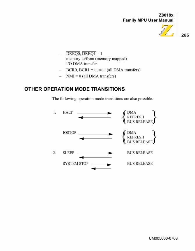
Z8018xFamily MPU User Manual
285
– DREQ0, DREQ1 = 1 memory to/from (memory mapped) I/O DMA transfer
– BCR0, BCR1 = 0000H (all DMA transfers)– NMI = 0 (all DMA transfers)
OTHER OPERATION MODE TRANSITIONS
The following operation mode transitions are also possible.
1. HALT DMAREFRESHBUS RELEASE
IOSTOP DMAREFRESHBUS RELEASE
2. SLEEP BUS RELEASE
SYSTEM STOP BUS RELEASE
{ }{ }
UM005003-0703

Z8018xFamily MPU User Manual
286
UM005003-0703

Z8018xFamily MPU User Manual
287
Status Signals
PIN OUTPUTS IN EACH OPERATING MODE
Table 55 describes pin outputs in each operating mode.
Table 55. Pin Outputs in Each Operating Mode
Mode M1 MREQ IORQ RD WR RFSH HALT BUSACK STAddressBUS
DataBUS
CPUOperation
Op Code Fetch(1st Op Code)
0 0 1 0 1 1 1 1 0 A IN
Op Code Fetch (except 1 st Op Code)
0 0 1 0 1 1 1 1 1 A IN
MemRead 1 0 1 0 1 1 1 1 1 A IN
Memory Write 1 0 1 1 0 1 1 1 1 A OUT
I/O Read 1 1 0 0 1 1 1 1 1 A IN
I/O Write 1 1 0 1 0 1 1 1 1 A OUT
Internal Operation
1 1 1 1 1 1 1 1 1 A IN
Refresh 1 0 1 1 1 0 1 1 * A IN
InterruptAcknowledgeCycle(1st MachineCycle)
NMI 0 0 1 0 1 1 1 1 0 A IN
INT0 0 1 0 1 1 1 1 1 0 A IN
INT1, INT2 & Internal Interrupts
1 1 1 1 1 1 1 1 0 A IN
BUS RELEASE 1 Z Z Z Z 1 1 0 * Z IN
HALT 0 0 1 0 1 1 0 1 0 A IN
SLEEP 1 1 1 1 1 1 0 1 1 1 IN
UM005003-0703
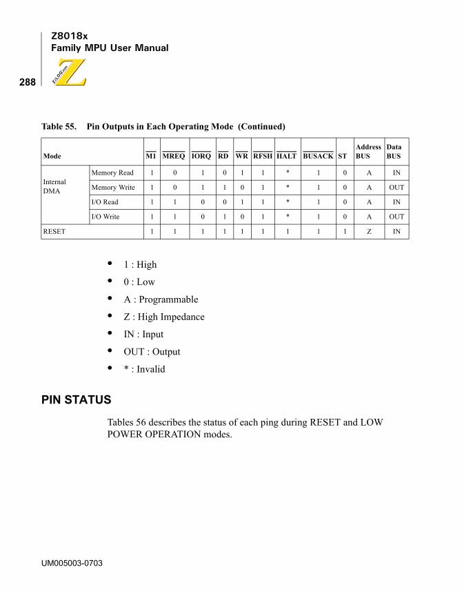
Z8018xFamily MPU User Manual
288
• 1 : High
• 0 : Low
• A : Programmable
• Z : High Impedance
• IN : Input
• OUT : Output
• * : Invalid
PIN STATUS
Tables 56 describes the status of each ping during RESET and LOW POWER OPERATION modes.
InternalDMA
Memory Read 1 0 1 0 1 1 * 1 0 A IN
Memory Write 1 0 1 1 0 1 * 1 0 A OUT
I/O Read 1 1 0 0 1 1 * 1 0 A IN
I/O Write 1 1 0 1 0 1 * 1 0 A OUT
RESET 1 1 1 1 1 1 1 1 1 Z IN
Table 55. Pin Outputs in Each Operating Mode (Continued)
Mode M1 MREQ IORQ RD WR RFSH HALT BUSACK STAddressBUS
DataBUS
UM005003-0703

Z8018xFamily MPU User Manual
289
Table 56. Pin Status During RESET and LOW POWER OPERATION Modes
Symbol Pin Function
Pin Status in Each Operation Mode
RESET SLEEP IOSTOPSYSTEM STOP
WAIT — IN (N) IN (N) IN (A) IN (N)
BUSACK — 1 OUT OUT OUT
BUSREQ — IN (N) IN (A) IN (A) IN (A)
RESET — 0 IN (A) IN (A) IN (A)
NMI — IN (N) IN (A) IN (A) IN (A)
INT0 — IN (N) IN (A) IN (A) IN (A)
INT1 — IN (N) IN (A) IN (A) IN (A)
INT2 — IN (N) IN (A) IN (A) IN (A)
ST — 1 1 OUT 1
A0–A17, A19 — Z 1 A 1
A18/TOUT A18 Z 1 A 1
TOUT Z OUT H H
D0–D7 — Z Z A Z
RTS0 — 1 H OUT H
CTS0 — IN (N) IN (A) IN (N) N (N)
DCD0 — IN (N) IN (A) IN (N) IN (N)
TXA0 — 1 OUT H H
RXA0 — IN (N) IN (A) IN (N) IN (N)
CKA0/DREQ0 CKA0(Internal Clock Mode)
Z OUT Z Z
UM005003-0703
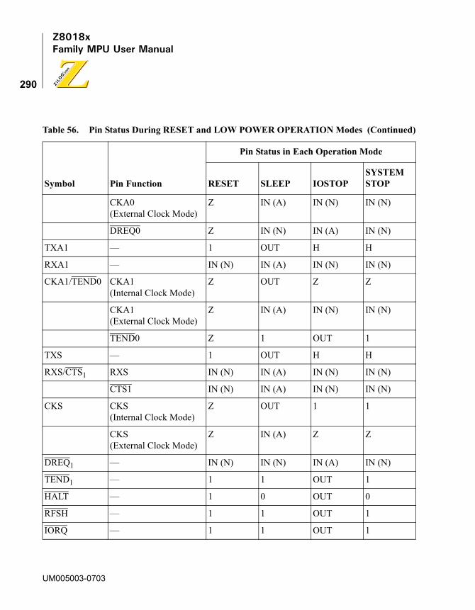
Z8018xFamily MPU User Manual
290
CKA0(External Clock Mode)
Z IN (A) IN (N) IN (N)
DREQ0 Z IN (N) IN (A) IN (N)
TXA1 — 1 OUT H H
RXA1 — IN (N) IN (A) IN (N) IN (N)
CKA1/TEND0 CKA1(Internal Clock Mode)
Z OUT Z Z
CKA1(External Clock Mode)
Z IN (A) IN (N) IN (N)
TEND0 Z 1 OUT 1
TXS — 1 OUT H H
RXS/CTS1 RXS IN (N) IN (A) IN (N) IN (N)
CTS1 IN (N) IN (A) IN (N) IN (N)
CKS CKS(Internal Clock Mode)
Z OUT 1 1
CKS(External Clock Mode)
Z IN (A) Z Z
DREQ1 — IN (N) IN (N) IN (A) IN (N)
TEND1 — 1 1 OUT 1
HALT — 1 0 OUT 0
RFSH — 1 1 OUT 1
IORQ — 1 1 OUT 1
Table 56. Pin Status During RESET and LOW POWER OPERATION Modes (Continued)
Symbol Pin Function
Pin Status in Each Operation Mode
RESET SLEEP IOSTOPSYSTEM STOP
UM005003-0703
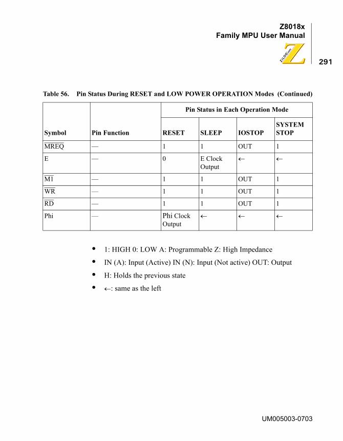
Z8018xFamily MPU User Manual
291
• 1: HIGH 0: LOW A: Programmable Z: High Impedance
• IN (A): Input (Active) IN (N): Input (Not active) OUT: Output
• H: Holds the previous state
• �: same as the left
MREQ — 1 1 OUT 1
E — 0 E Clock Output
� �
M1 — 1 1 OUT 1
WR — 1 1 OUT 1
RD — 1 1 OUT 1
Phi — Phi Clock Output
� � �
Table 56. Pin Status During RESET and LOW POWER OPERATION Modes (Continued)
Symbol Pin Function
Pin Status in Each Operation Mode
RESET SLEEP IOSTOPSYSTEM STOP
UM005003-0703

Z8018xFamily MPU User Manual
292
UM005003-0703
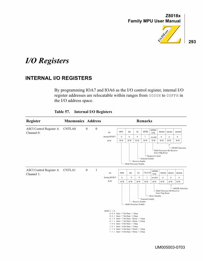
Z8018xFamily MPU User Manual
293
I/O Registers
INTERNAL I/O REGISTERS
By programming IOA7 and IOA6 as the I/O control register, internal I/O register addresses are relocatable within ranges from 0000H to 00FFH in the I/O address space.
Table 57. Internal I/O Registers
Register Mnemonics Address Remarks
ASCI Control Register A Channel 0:
CNTLA0 0 0
ASCI Control Register A Channel 1:
CNTLA1 0 1
MPE RE TE RTS0MPBR/
EFR MOD2 MOD1 MOD0
R/W R/WR/W R/W R/W R/W R/W R/W
MODE SelectionMulti Processor Bit Receive/Error Flag Reset
Request to SendTransmit Enable
Receive EnableMulti Processor Enable
invalid0 10 0 0 0 0
1
bit
during RESET
R/W
R/W R/W R/W R/W R/W R/W R/W R/W
MODE SelectionMulti Processor Bit Receive/Error Flag Reset
0 0 10 0 0 0
MPE RE TE MOD2 MOD1 MOD0CKA1DMPBR/EFR
invalid
Transmit EnableReceive Enable
Multi Processor Enable
CKA1 Disable
MOD 2 1 0 0 0 0 Start + 7 bit Data + 1 Stop0 0 1 Start + 7 bit Data + 2 Stop0 1 0 Start + 7 bit Data + Parity + 1 Stop0 1 1 Start + 7 bit Data + Parity + 2 Stop1 0 0 Start + 8 bit Data + 1 Stop1 0 1 Start + 8 bit Data + 2 Stop1 1 0 Start + 8 bit Data + Parity + 1 Stop1 1 1 Start + 8 bit Data + Parity + 2 Stop
bit
during RESET
R/W
UM005003-0703

Z8018xFamily MPU User Manual
294
ASCI Control Register B Channel 0:
CNTLB0 0 2
ASCI Control Register B Channel 1:
CNTLB1 0 3
Table 57. Internal I/O Registers (Continued)
Register Mnemonics Address Remarks
MPBT MP CTS/PS PEO DR SS2 SS1 SS0bit
during RESET
R/W
0 0 0* 1 11
R/W R/W R/W R/W R/W R/W R/W R/W
Clock Source andSpeed SelectDivide Ratio
Parity Even or OddClear to send/Prescale
Multi ProcessorMulti Processor Bit Transmit
* CTS: Depending on the condition 0f CTS Pin.PS: Cleared to 0.
invalid
MPBT MPCTS/
PEO DR SS2 SS1 SS0
R/W R/WR/W R/W R/W R/W R/W R/W
Clock Source and
Divide Ratio
Clear to Send/PrescaleMulti Processor
Multi Processor Bit Transmit
0invalid 00 0 1 1 1
bit
during RESET
R/W
PS
Speed Select
Parity Even or Odd
Generaldivide ratio
PS=0(divide ratio=10)
PS=1(divide ratio=30)
SS2 1 0
0 0 00 0 10 1 00 1 11 0 01 0 11 1 0
1 1 1
� � 160� � � � � �
� � � � � � � �
320
10240512025601280
640
� � 640� � � � � �
128025605120
102402048040960
� � 480� � � � � �
960192038407680
1536030720
192038407680
153603072061440
122880
External clock (frequency < � ��40)
DR=0 (X 16) DR=1 (X 64) DR=0 (X 16) DR=1 (X 64)
UM005003-0703

Z8018xFamily MPU User Manual
295
rupt Enableister Empty
rupt Enableister Empty
ASCI Status Channel 0: STAT0 0 4
ASCI Status Channel 1: STAT1 0 5
Table 57. Internal I/O Registers (Continued)
Register Mnemonics Address Remarks
R R R R R/W R R R/W
Transmit Inter
0 0 00 * ** 0
RDRF OVRN PE DCD0 TDRE TIEFE
invalid
bit
during RESET
R/W
RIE
Transmit Data RegData Carrier Detect
Receive Interrupt Enable
Framing ErrorParity Error
Overrun ErrorReceive Data Register Full
TDREL
H
1
0
** CTS0 Pin
* DCD0: Depending on the condition of DCD0 Pin.
R R R R R/W R R R/W
Transmit Inter
0 0 00 0 1 0
RDRF OVRN PE CTS1E TDRE TIEFE
0
bit
during RESET
R/W
RIE
Transmit Data RegCTS1 Enable
Receive Interrupt Enable
Framing ErrorParity Error
Overrun ErrorReceive Data Register Full
UM005003-0703
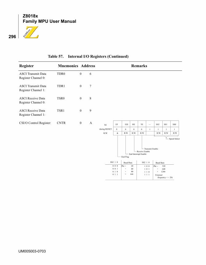
Z8018xFamily MPU User Manual
296
ASCI Transmit Data Register Channel 0:
ASCI Transmit Data Register Channel 1:
ASCI Receive Data Register Channel 0:
ASCI Receive Data Register Channel 1:
CSI/O Control Register:
TDR0
TDR1
TSR0
TSR1
CNTR
0 6
0 7
0 8
0 9
0 A
Table 57. Internal I/O Registers (Continued)
Register Mnemonics Address Remarks
EF EIE TE — SS2 SS1 SS0
R R/WR/W R/W R/W R/W R/W
Receive EnableEnd Interrupt Enable
End Flag
10 00 0 1 1 1
bit
during RESET
R/W
Speed Select
Transmit Enable
RE
SS2 1 0
0 0 00 0 10 1 00 1 1
Phi � 20� � �
40
16080
External
Baud Rate SS2 1 0
1 0 01 0 11 1 01 1 1
Phi � 320� �
6401280
Baud Rate
frequency < ��20)
UM005003-0703
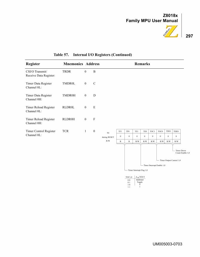
Z8018xFamily MPU User Manual
297
1,0
CSI/O Transmit/Receive Data Register:
Timer Data Register Channel 0L:
Timer Data Register Channel 0H:
Timer Reload Register Channel 0L:
Timer Reload Register Channel 0H:
Timer Control Register Channel 0L:
TRDR
TMDR0L
TMDR0H
RLDR0L
RLDR0H
TCR
0 B
0 C
0 D
0 E
0 F
1 0
Table 57. Internal I/O Registers (Continued)
Register Mnemonics Address Remarks
R R R/W R/W R/W R/W R/W R/W
0 0 00 0 0 0
TF1 TF0 TE1 TOC0 TDE1 TDE0TE0
0
bit
during RESET
R/W
TOC1
A18/TOUT0 0 Inhibited
TOC1,0
Timer DownCount Enable
Timer Output Control 1,0
Timer Interrupt Enable 1,0
Timer Interrupt Flag 1,0
Toggle01
0 11 01 1
UM005003-0703
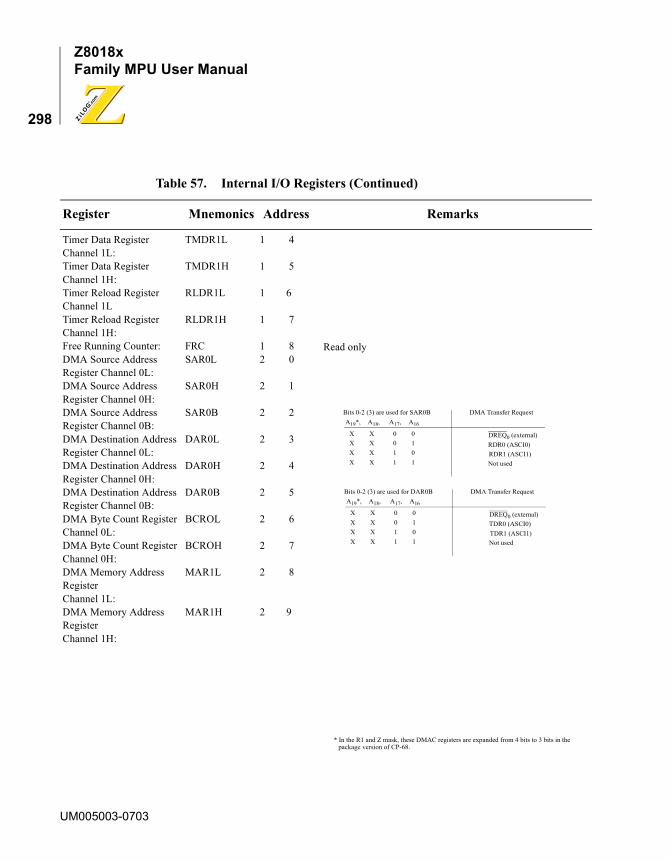
Z8018xFamily MPU User Manual
298
Timer Data Register Channel 1L:Timer Data Register Channel 1H:Timer Reload Register Channel 1LTimer Reload Register Channel 1H:Free Running Counter:DMA Source Address Register Channel 0L:DMA Source Address Register Channel 0H:DMA Source Address Register Channel 0B:DMA Destination Address Register Channel 0L:DMA Destination Address Register Channel 0H:DMA Destination Address Register Channel 0B:DMA Byte Count Register Channel 0L:DMA Byte Count Register Channel 0H:DMA Memory Address Register Channel 1L:DMA Memory Address Register Channel 1H:
TMDR1L
TMDR1H
RLDR1L
RLDR1H
FRCSAR0L
SAR0H
SAR0B
DAR0L
DAR0H
DAR0B
BCROL
BCROH
MAR1L
MAR1H
1 4
1 5
1 6
1 7
1 82 0
2 1
2 2
2 3
2 4
2 5
2 6
2 7
2 8
2 9
Table 57. Internal I/O Registers (Continued)
Register Mnemonics Address Remarks
Bits 0-2 (3) are used for SAR0BA19*, A18, A17, A16
XXXX
XXXX
0011
0101
DMA Transfer Request
DREQ0 (external)RDR0 (ASCI0)RDR1 (ASCI1)Not used
Bits 0-2 (3) are used for DAR0BA19*, A18, A17, A16
XXXX
XXXX
0011
0101
DMA Transfer Request
DREQ0 (external)TDR0 (ASCI0)TDR1 (ASCI1)Not used
* In the R1 and Z mask, these DMAC registers are expanded from 4 bits to 3 bits in thepackage version of CP-68.
Read only
UM005003-0703
Z8018xFamily MPU User Manual
299
DMA Memory Address Register Channel 1B:
DMA I/O Address Register Channel 1L:
DMA I/O Address Register Channel 1H
DMA Byte Count Register Channel 1L:
DMA Byte Count Register Channel 1H:
DMA Status Register:
DMA Mode Register:
MAR1B
IAR1L
IAR1H
BCR1L
BCR1H
DSTAT
DMODE
2 A
2 B
2 C
2 E
2 F
3 0
3 1
Table 57. Internal I/O Registers (Continued)
Register Mnemonics Address Remarks
DE1 DE0 DWE0 DIE1 DIE0 — DME
R/W R/WR/W W W R
DMA Enable Bit Write Enable 1,0DMA enable ch 1,0
00 10 1 0 1 0
bit
during RESET
R/W
DMA Master enable
DMA Interrupt Enable 1,0
DM1,0
0 0 0 1 1 01 1
MM
I/OM
Destination
DWE1
Address
DAR0+1DAR0-1DAR0 fixedDAR0 fixed
— — DM0 SM1 SM0 MMOD —
R/WR/W R/W R/W
Ch 0 Destination Mode 1,0
01 01 0 0 0 1
bit
during RESET
R/W
Memory MODE select
Ch 0 Source Mode 1,0
DM1
R/W
SM1,0
0 0 0 1 1 01 1
MM
I/OM
Source Address
SAR0+1SAR0-1SAR0 fixedSAR0 fixed
MMOD Mode
01
Cycle Steal ModeBurst Mode
R/W
Bits 0 - 2 are used for MAR1B
UM005003-0703

Z8018xFamily MPU User Manual
300
MMU Common Base Register:
MMU Bank Base Register
MMU Common/Bank Register
Operation Mode Control Register
I/O Control Register:
CBR
BBR
CBAR
OMCR
ICR
3 8
3 9
3 A
3 E
3 F
Table 57. Internal I/O Registers (Continued)
Register Mnemonics Address Remarks
R/W R/W R/W
0 0 00 0 0 0
CB7 CB6 CB5
0
bit
during RESET
R/W
MMU Common Base Register
R/W R/W
1 1 11 0 0 00
bit
during RESET
R/W
MMU Common Area Register
R/W R/W
MMU Bank
CB4 CB3 CB2 CB1 CB0
R/W R/W R/W R/W R/W
R/W R/W R/W
0 0 00 0 0 0
BB7 BB6 BB5
0
bit
during RESET
R/W
MMU Bank Base Register
BB4 BB3 BB2 BB1 BB0
R/W R/W R/W R/W R/W
CA3 CA2 CA1 CA0 BA3 BA2 BA1 BA0
R/W R/W R/W R/W
R/W
1 1 11 1 1 11
bit
during RESET
R/W
M1 Enable
I/O Compatibility
MIE MITE IOC —
W R/W
— — — —
M1 Temporary Enable
R/W
0 0 10 1 1 11
bit
during RESET
R/W
I/O Address
I/O Stop
IOA7 —
R/W
— — — —IOA6 IOSTP
R/W
Area Register
UM005003-0703

Z8018xFamily MPU User Manual
301
DMA/WAIT Control Register:
DCNTL 3 2
Table 57. Internal I/O Registers (Continued)
Register Mnemonics Address Remarks
R/W R/W R/W R/W R/W R/W R/W R/W
1 1 11 0 0 0
MWI1 MWI0 IWI1 DMS0 DIMA1 DIMA0IWI0
0
bit
during RESET
R/W
DMS1
The number of
0 0MWI1,0
DMA Ch 1I/O Memory
I/O Wait InsertionMemory Wait Insertion
010 1
1 01 1
Mode Select
wait states
23
The number of
0 0IWI1,0
020 1
1 01 1
wait states
34
1DMSi
Edge sense0
Sense
Level sense
0 0
DIM1,0
M�I/O0 11 01 1
Transfer Mode
M�I/OI/O�MI/O�M
MAR1+1
Address Increment/Decrement
MAR1-1IAR1 fixedIAR1 fixed
IAR1 fixedIAR1 fixedMAR1+1MAR1-1
DREQi Select, i=1,0
UM005003-0703
Z8018xFamily MPU User Manual
302
0
Interrupt Vector Low Register
INT/TRAP Control Register
Refresh Control Register:
IL
ITC
RCR
3 3
3 4
3 6
Table 57. Internal I/O Registers (Continued)
Register Mnemonics Address Remarks
R/W R/W R/W
0 0 00 0 0 0
IL7 IL6 IL5 — — ——
0
bit
during RESET
R/W
—
Interrupt Vector Low
R/W R R/W
0 0 11 0 0 0
TRAP UF0 — —
1
bit
during RESET
R/W
—
Unidentified Fetch Object
ITE2 ITE1 ITE0
R/W R/W
INT Enable 2,1,
TRAP
R/W R/W
1 1 11 1 0 0
REFE REFW — —
1
bit
during RESET
R/W
—
Refresh Wait State
CYC1 CYC0
R/W R/W
Cycle select
Refresh Enable
—
0 0 10 states200 1
1 01 1
Interval of Refresh Cycle
4080
UM005003-0703

Z8018xFamily MPU User Manual
303
ORDERING INFORMATION
Codes
• PackageP = Plastic DipV = Plastic Chip CarrierF = Quad Flat Pack
• TemperatureS = 0�C to +70�CE = -40�C to 100�C
• Speed06 = 6 MHz08 = 8 MHz10 = 10 MHz
• EnvironmentalC = Plastic Standard
• ExampleZ8018008PSC is an 80180 8 MHz, Plastic DIP, 0�C to70�C, Plastic Standard Flow.
Z 80180 08 P S C
Environmental FlowTemperature
PackageSpeedProduct Number
ZiLOG Prefix
UM005003-0703

Z8018xFamily MPU User Manual
304
UM005003-0703

Z8018xFamily MPU User Manual
305
AAC characteristics 197Address generation, physical 64Address map
I/O 44I/O address translation 57Logical examples 55Logical memory organization 58Logical space configuration 59Physical address transition 56
AddressingExtended 182I/O 184Indexed 182Indirect 181
Architecture 12ASCI
Baud rate selection 142Block diagram 117Clock diagram 141Control register A0 125Control register A1 128Control register B 131Functions 116Interrupt request circuit diagram 140Register descriptions 117Status register 0 120Status register 1 123
Asynchronous serial communications interface (ASCI) 14
BBaud rate selection
ASCI 142CSI/O 150
Block diagram 6ASCI 117CSI/O 146DMAC 92MMU 56PRT 157
Bus state controller 13
CCentral processing unit (CPU) 14Circuit diagram, ASCI interrupt request 140Clock generator 13Clocked serial I/O (CSI/O) 14CPU register configurations 176CPU timing
Basic instruction 23BUSREQ/BUSACK Bus Exchange 25HALT and Low Power modes 31I/O data read/write 22Internal I/O registers 41MMU register description 60Op Code fetch timing 18Operand and data read/write 20RESET 25Wait state generator 27
UM005003-0703
Z8018xFamily MPU User Manual
306
CSI/OBaud rate selection 150Block diagram 146Control/Status register 147, 150, 159,
160, 161, 172External clock receivetiming diagram 156External clock transmit timing diagram
154Internal clock receivetiming diagram 155Internal clock transmit timing diagram
153interrupt request generation 151Operation 151Receive/Transmit timing diagram 204Timer initialization, count down and reload
timing diagram 163Timer output control 163Timer output timing diagram 164
Cycle timing 87
DData formats 131DC characteristics
Absolute maximum ratings 185Z80180 186Z8L180 189Z8S180 187
DCD0 timing diagram 139Description, general 1Design rules, circuit board 170
Direct register bit field definitions 181Divide ratio 134DMA
Controller (DMAC) 90CYCLE STEAL mode timing diagram
106Edge-sense timing diagram 108Interrupt request generation 114Level-sense timing diagram 107Mode register (DMODE) 97Operation 104Status register (DSTAT) 95TEND0 output timing diagram 108Transfer request 110WAIT control register 100
DMACBlock diagram 92Register 93
DRAM refresh intervals 89Dynamic RAM refresh control 86
EE clock
BUS RELEASE, SLEEP and SYSTEM STOP modes timing diagram 201
Memory and I/O R/W cycles timing dia-gram 201
Minimum timing example of PWEL and PWEH timing diagram 202
Timing conditions 166Timing diagram (R/W and INTACK cy-
UM005003-0703
Z8018xFamily MPU User Manual
307
cles) 167Timing diagram (SLEEP and SYSTEM
STOP modes) 168Extended addressing 182External clock rise and fall time 204
FFeatures 1
HHALT mode 31
II/O
Addressing 184Control register (ICR) 42
I/O control register 42Immediate addressing
AddressingImmediate 183
Indexed addressing 182Indirect addressing 181Input ris and fall time (except EXTAL and RE-SET) timing diagram 204Instruction set
CPU registers 175Flag register 178Summary 173
INT0Interrupt mode 2 timing 80Mode 1 interrupt sequence 77Mode 1 timing 78
INT0 mode 0 timing 76Interrupt
Acknowledge cycle timings 82Control registers and flags 65Controller 13CSI/O request generation 151DMA request generation 114Enable (ITE) 68INT/TRAP control register (ITC) 67Maskable interrupt 0 (INT0) 75Non-maskable 72PRT request generation 164Sources 65Sources during reset 83TRAP 70Vector register (I) 66
IOSTOP mode 35
LLevel-sense programming 109Logical memory organization 58
MM1 temporary enable timing 16Maskable interrupt level 0 75
UM005003-0703

Z8018xFamily MPU User Manual
308
Memory and I/O Wait state insertion 29Memory management unit (MMU) 13Memory to ASCI 109Memory to memory 105MMU Register description 60Mode
HALT 31IOSTOP 35SLEEP 33SYSTEM STOP 35
Modem control signals 138
NNMI
and DMA operation timing diagram 115Use 74
Non-maskable interrupt 72
OOn-chip clock generator
Circuit board design rules 170External clock interface 169Operating frequencies 168
Operation modesControl register 84CPU timing 18IOC 16M1 Enable 15M1 temporary enable 16
PPin description
A0 through CTS1 7BUSREQ through RFSH 9D0 through INT2 8RTS0 through TEND1 10TEST through XTAL 10
Pin package64-pin DIP 368-pin PLCC 480-pin QFP 5
Programmable reload timer (PRT) 14Programming
Level-sense 109PRT
Block diagram 157Bus release mode timing diagram 167Interrupt request generation 164Timer control register 161
RRefresh 87
Control register 88Register
ASCI Control A0 125ASCI Control A1 128ASCI Control B 131ASCI Status 0 120ASCI Status 1 123
UM005003-0703
Z8018xFamily MPU User Manual
309
CSI/O control/status 147, 150, 159, 160, 161, 172
Direct bit field definitions 181DMA mode (DMODE) 97DMA status 95DMA/WAIT control 100Flag 178I/O Control 42I/O control (ICR) 42Indirect addressing 181INT/TRAP control (ITC) 67Interrupt Vector (I) 66MMU bank base (BBR) 62MMU common bank area (CBAR) 60MMU common base (CBR) 61Operation mode control 15, 84PRT timer control register 161Refresh control 88
Relative addressingAddressing
Relative 183RETI
control signal states 85Instruction sequence 84
RTS0 timing diagram 140
SSecondary bus interface 165SLEEP mode 33SLP execution cycle timing diagram
Timing diagramSLP execution cycle 203
Status summary table 10SYSTEM STOP mode 35
TTest conditions, standard 205Timer initialization, count down and reload 163Timer output timing diagram
Timing diagramTimer output 202
Timing diagram 163AC 197Bus Exchange Timing During CPU Inter-
nal Operation 27Bus Exchange Timing During Memory
Read 26CPU (I/O Read/Write cycles) 199CSI/O external clock receive 156CSI/O external clock transmit 154CSI/O internal clock receive 155CSI/O internal clock transmit 153CSI/O receive/transmit 204CSI/O timer output 164DCD0 139DMA control signals 200DMA CYCLE STEAL mode 106DMA edge-sense 108DMA level-sense 107
UM005003-0703

Z8018xFamily MPU User Manual
310
DMA TEND0 output 108E clock (memory and I/O R/W cycles) 201E clock (R/W and INTACK cycles) 167E clock (SLEEP and SYSTEM STOP
modes) 168E clock BUS RELEASE, SLEEP and SYS-
TEM STOP modes) 201E clock minimum timing example of
PWEL and PWEH) 202External clock rise and fall 204HALT 33I/O Read and Write cycles with IOC = 0 17I/O read and write cycles with IOC=1 17I/O read/write timing 23Input rise and fall time 204Instruction 24INT0 interrupt mode 2 80INT0 mode 0 76INT0 mode 1 78INT1, INT2 and Internal interrupts 86M1 temporary enable 16Memory read/write timing (with Wait
state) 22Memory read/write timing (without Wait
state) 21NMI and DMA operation 115Op Code Fetch timing (with Wait state) 20Op Code Fetch timing (without Wait state)
19PRT bus release mode 167Refresh cycle 87RESET 25RTS0 140
SLEEP 35TRAP timing - 2nd Op Code Undefined 71TRAP timing - 3rd Op Code Undefined 72WAIT 28
TRAP 68Interrupt 70Timing 71
UUndefined Fetch Object (UFO) 68
VVector acquisition
INT0 mode 2 79INT1, INT2 81
Vector table 82
WWait state generation
I/O Wait insertion 29Memory and 29Programmable Wait state insertion 28Wait input and reset 30
Wait state insertion 30
UM005003-0703