Yamaha s08
55
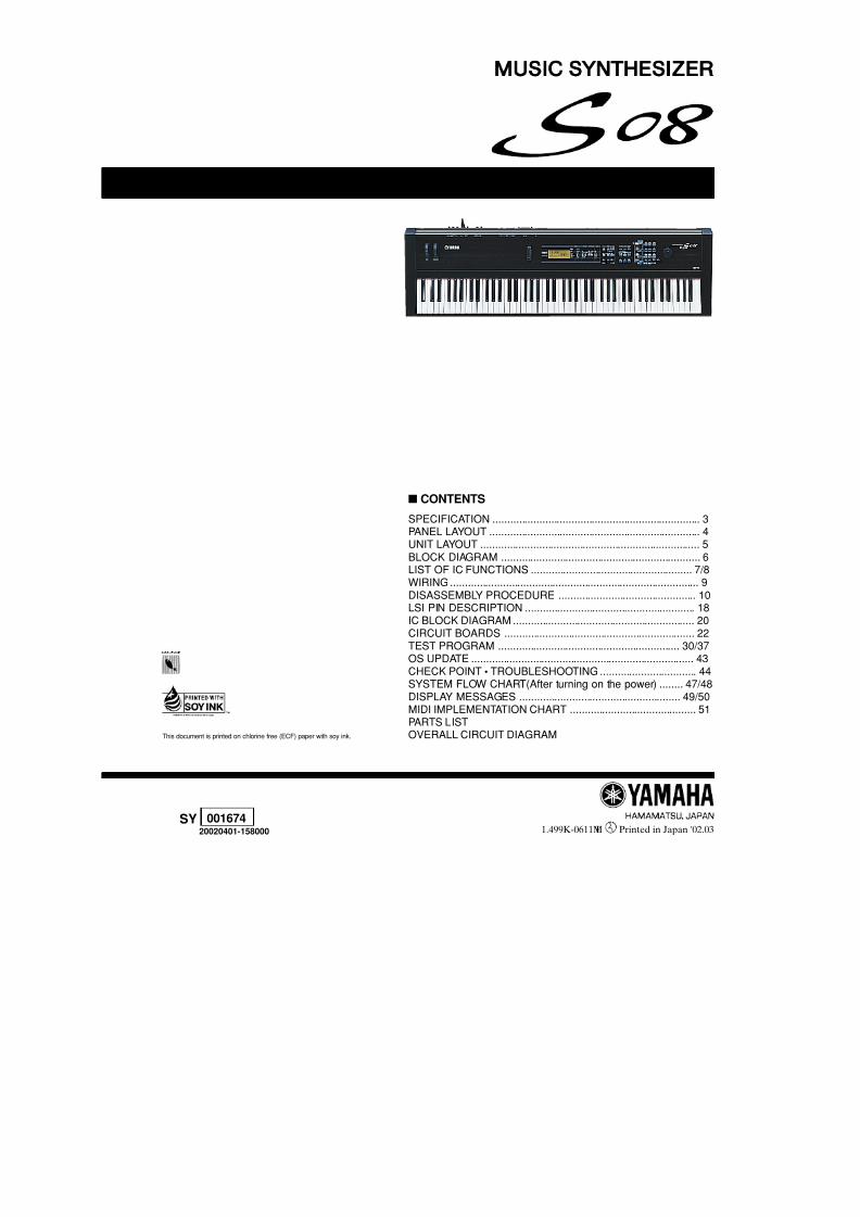
1.499K-0611 I M Printed in Japan '02.03 SERVICE MANUAL SY 001674 This document is printed on chlorine free (ECF) paper with soy ink. 20020401-158000 s CONTENTS SPECIFICA TION ....................................................................... 3 P ANEL LA YOUT ........................ ........... ..................................... 4 UNIT LA YOUT ........................................................................... 5 BLOCK DIA GRAM .......... .......................................................... 6 LIST OF IC FUNCTIONS ....................................................... 7/8 WIRING ............ ........... .............................................................. 9 DISASSEMBL Y PROCEDURE ............................................... 10 LSI PIN DESCRIPTION .......................................................... 18 IC BLOCK DIAGRAM .............................................................. 20 CIRCUIT BOARDS ................................................................. 22 TEST PROGRAM .............................................................. 30/37 OS UPDA TE ............................................... ............ ................. 43 CHECK POINT • TROUBLESHOOTING ................................. 44 SYSTEM FLOW CHART(After t urning on t he power ) ........ 47/48 DISPLA Y MESSAGES .................................... ........... ........ 49/50 MIDI IMPLEMENT A TION CHART ........................................... 51 P ARTS LIST OVERALL CIRCUIT DIAGRAM
Transcript of Yamaha s08
7/22/2019 Yamaha s08
http://slidepdf.com/reader/full/yamaha-s08 1/69
SERVICE MANUAL
7/22/2019 Yamaha s08
http://slidepdf.com/reader/full/yamaha-s08 2/69
S08
IMPORTANT NOTICE
This manual has been provided for the use of authorized Yamaha Retailers and their service personnel. It has been assumed that basic
service procedures inherent to the industry, and more specifically Yamaha Products, are already known and understood by the users,
and have therefore not been restated.
WARNING: Failure to follow appropriate service and safety procedures when servicing this product may result in personal injury,
destruction of expensive components, and failure of the product to perform as specified. For these reasons, we
advise all Yamaha product owners that all service required should be performed by an authorized Yamaha Retailer or
the appointed service representative.
IMPORTANT: The presentation or sale of this manual to any individual or firm does not constitute authorization, certification or
recognition of any applicable technical capabilities, or establish a principle-agent relationship of any form.
The data provided is believed to be accurate and applicable to the unit(s) indicated on the cover. The research, engineering, and
service departments of Yamaha are continually striving to improve Yamaha products. Modifications are, therefore, inevitable and
changes in specification are subject to change without notice or obligation to retrofit. Should any discrepancy appear to exist, pleasecontact the distributor's Service Division.
WARNING: Static discharges can destroy expensive components. Discharge any static electricity your body may have
accumulated by grounding yourself to the ground bus in the unit (heavy gauge black wires connect to this bus).
IMPORTANT: Turn the unit OFF during disassembly and part replacement. Recheck all work before you apply power to the unit.
LITHIUM BATTERY HANDLINGThis product uses a lithium battery for memory back-up.
WARNING: Lithium batteries are dangerous because they can be exploded by improper handling. Observe the followingprecautions when handling or replacing lithium batteries.
• Leave lithium battery replacement to qualified service personnel.• Always replace with batteries of the same type.• When installing on the PC board by soldering, solder using the connection terminals provided on the battery cells.
Never solder directly to the cells. Perform the soldering as quickly as possible.• Never reverse the battery polarities when installing.• Do not short the batteries.• Do not attempt to recharge these batteries.• Do not disassemble the batteries.• Never heat batteries or throw them into fire.
7/22/2019 Yamaha s08
http://slidepdf.com/reader/full/yamaha-s08 3/69
S08
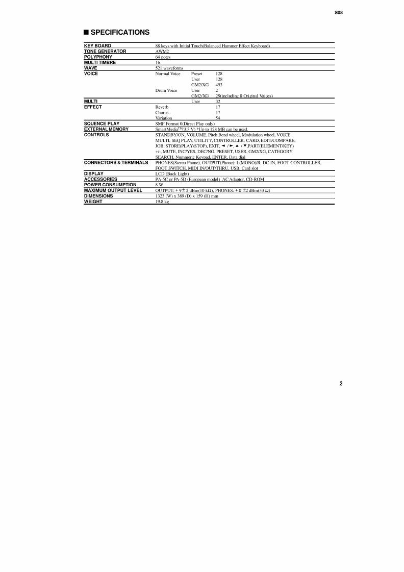
s SPECIFICATIONS
KEY BOARD
TONE GENERATOR
POLYPHONY
MULTI TIMBRE
WAVE
VOICE
MULTI
EFFECT
SQUENCE PLAY
EXTERNAL MEMORY
CONTROLS
CONNECTORS & TERMINALS
DISPLAY
ACCESSORIES
POWER CONSUMPTION
MAXIMUM OUTPUT LEVEL
DIMENSIONS
WEIGHT
88 keys with Initial Touch(Balanced Hammer Effect Keyboard)
AWM2
64 notes
16
521 waveforms
Normal Voice Preset 128
User 128
GM2/XG 493
Drum Voice User 2
GM2/XG 29(including 8 Original Voices)
User 32
Reverb 17Chorus 17
Variation 54
SMF Format 0(Direct Play only)
SmartMediaTM(3.3 V) *Up to 128 MB can be used.
STANDBY/ON, VOLUME, Pitch Bend wheel, Modulation wheel, VOICE,
MULTI, SEQ PLAY, UTILITY, CONTROLLER, CARD, EDIT/COMPARE,
JOB, STORE(PLAY/STOP), EXIT, Q / W, H / G,PART(ELEMENT/KEY)
+/-, MUTE, INC/YES, DEC/NO, PRESET, USER, GM2/XG, CATEGORY
SEARCH, Nummeric Keypad, ENTER, Data dial
PHONES(Stereo Phone), OUTPUT(Phone): L(MONO)/R, DC IN, FOOT CONTROLLER,FOOT SWITCH, MIDI IN/OUT/THRU, USB, Card slot
LCD (Back Light)
PA-5C or PA-5D (European model) AC Adaptor, CD-ROM
8 W
OUTPUT: + 9 2 dBm(10 k Ω), PHONES: + 0 2 dBm(33 Ω)
1323 (W) x 389 (D) x 159 (H) mm
19.8 kg
7/22/2019 Yamaha s08
http://slidepdf.com/reader/full/yamaha-s08 4/69
S08
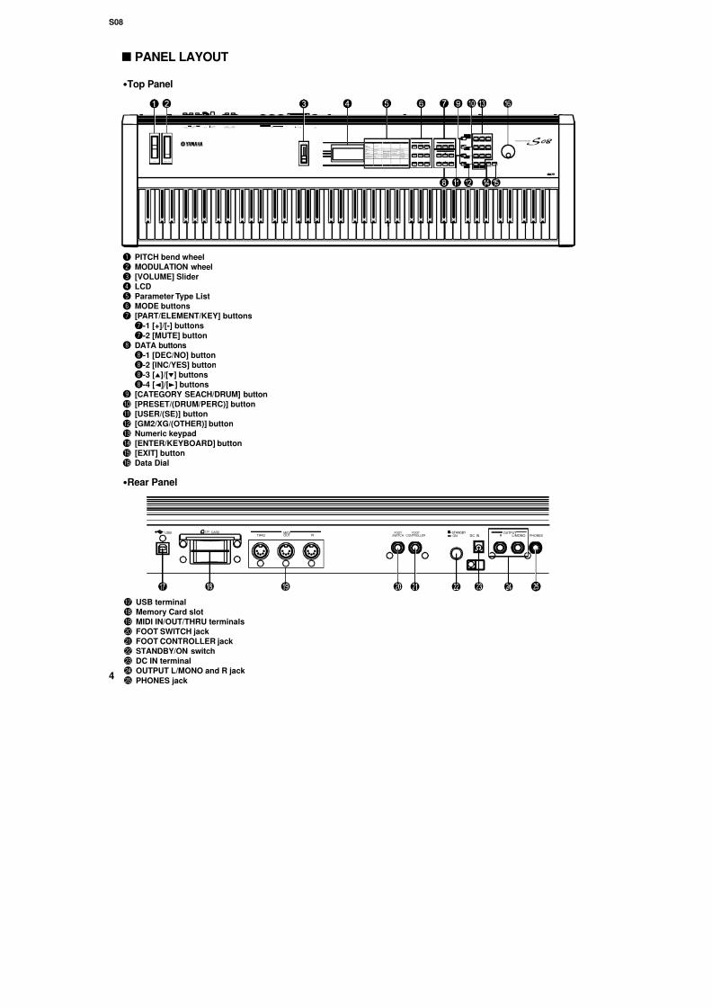
s PANEL LAYOUT
MUSICSYNTHESIZER
EXITENTER
KEYBOARD
– 0
1 2 3
4 5 6
7 8 9
PRESET
USER
GM2/XG
DRUM
MUTE+ –
COMMON
INC/YESDEC/NO
DEMO
UTILITYCONTROLLER CARD
E DIT JO B STO RE
PLAY/STOPCOMPARE
V O IC E M UL T I S E Q P L AYPART/ COMMON
VOICE
MIX
GENERAL
TONE
CONTROLLER
EFFECT
ELEMENT
OS C/MIX
PITCH
FILTER
AMP
LFO
EFFECT
TG
MIDI CHANNEL
MIDI FILTER
SEQ SETUP
MIDI S E TUP
EFFECT
CTRL ASSIGN
KEYBOARD
VELOCITY
CTRL S E TUP
SAVE
LOAD
RENAME
DELETE
FORMAT
IMPORT
VOLUME
PITCH MODULATION
P HONES L /MONOOUTPUT
R DC IN ONSTANDBY FOOT
CONTROLLERFOOT
SWITCH IN OUT THRUMIDI
CARD3.3V USB
GUITARORGANPIANO
CATEGORYSEARCH
B A SS S T RI N GS B RA S S
REED/PIPE SYNLEAD
SYNCOMP
DRUM/PERC
SE
OTHER CHROMATICPERCUSSION
SYNPAD
UTILITY
CARD
CONTROLLER
CARDUTILITYEDIT CONTROLLER PART/ELEMENT/KEYMODE
DATA
•Top Panel
q PITCH bend wheel
w MODULATION wheel
e [VOLUME] Slider
r LCDt Parameter Type List
y MODE buttons
u [PART/ELEMENT/KEY] buttons
u-1 [+]/[-] buttons
u-2 [MUTE] button
i DATA buttons
i-1 [DEC/NO] button
i-2 [INC/YES] button
i-3 [H]/[G] buttons
i 4 [Q]/[W] buttons
7/22/2019 Yamaha s08
http://slidepdf.com/reader/full/yamaha-s08 5/69
S08
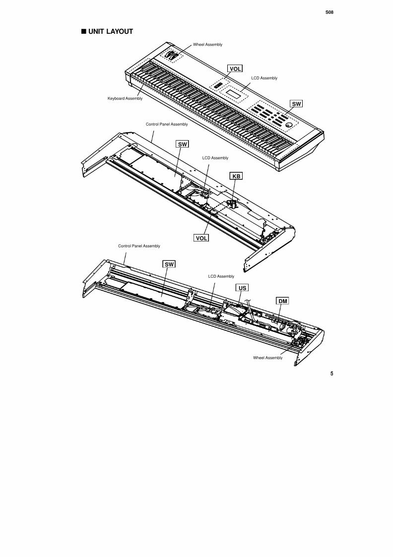
s UNIT LAYOUT
KB
Keyboard Assembly
Wheel Assembly
LCD Assembly
SW
Control Panel Assembly
LCD Assembly
SW
VOL
7/22/2019 Yamaha s08
http://slidepdf.com/reader/full/yamaha-s08 6/69
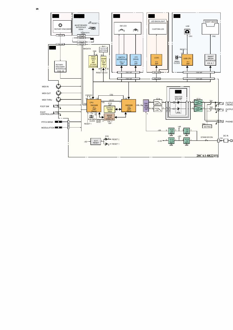
6
ROTARY ENCODER
ROTARYENCODERINTERFACE
88 KEYBOARDINTERFACE
KSN2
ROM16Mbit
(FLASH)PROGRAM
BACKUPBATTERY
SRAM
1Mbitx2
SWITCHINTERFACE
LEDDRIVE
LCDC
16MHz
CLOCK
USB CPU
S
USB
LED BACKLIGHT
CUSTOM LCD
SW LED
8.4672MHzCLOCK
EFFECTDRAM4Mbit
WAVEROM
64Mbit X2
SWX00B SWX00BDAC18bit
LPF
VOL
AMP
AMP
MASTERVOLUME
MU
MIDI IN
MIDI OUT
MIDI THRU
FOOT SW
FOOTCONTROLLER
PITCH BEND
DM
SW
KB
GH-D_SW HHE-D_SW L SW LC US
VOL
CPU
SlaveMaster
CN2-4P CN1-8P
CN5-8P
CN4-6P
CN3-6PCN2-4P
IC26, 29
32
B+1
IC5
48P
IC3, 4
32P
IC1168P
9
IC1240P
IC6, 744P
IC2168P
158 15
IC1816P
11 3
6 5
3
5
1
7
1
7
C N 1 - 6 P
IC13
IC2, 320P
IC420P
IC180P
IC180P
14
CN1
CN1-15P CN5-36P
CN7-36PCN4-15P
CN1-14P
CN6-14P
N 5 - 5 P
IC16
LPF C N 3 - 6 P
TR3
7
9A
20
23
26RESET 1
154
MKDATA
MKDATA
CS0
26
30
RESET 2 CS1
22
46 93
CS0CS1
125
132 150
1
LSI IC
CS2
RESET 1
7374
SCS0SCS1
1
12
10
RESET 1
7/22/2019 Yamaha s08
http://slidepdf.com/reader/full/yamaha-s08 7/69
S08
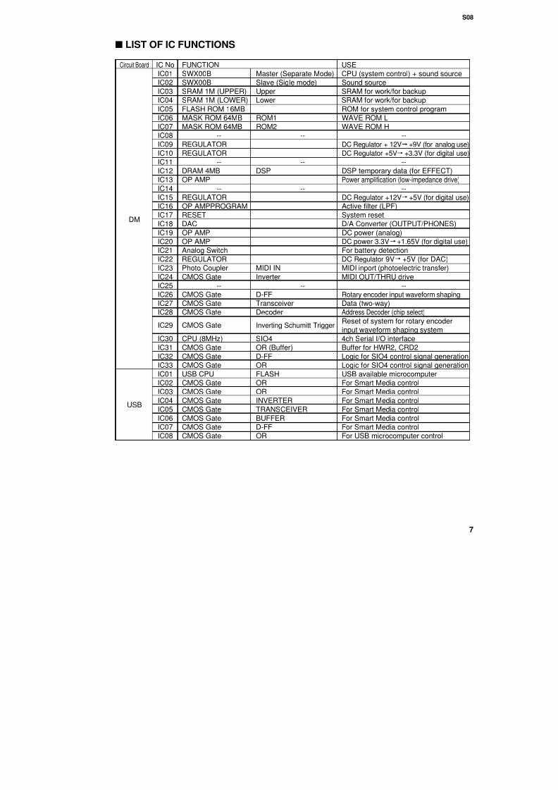
s LIST OF IC FUNCTIONS
Circuit Board IC No FUNCTION USE
IC01 SWX00B Master (Separate Mode) CPU (system control) + sound sourceIC02 SWX00B Slave (Sigle mode) Sound source
IC03 SRAM 1M (UPPER) Upper SRAM for work/for backup
IC04 SRAM 1M (LOWER) Lower SRAM for work/for backup
IC05 FLASH ROM 16MB ROM for system control program
IC06 MASK ROM 64MB ROM1 WAVE ROM L
IC07 MASK ROM 64MB ROM2 WAVE ROM H
IC08 -- -- --
IC09 REGULATOR DC Regulator + 12V +9V (for analog use)
IC10 REGULATOR DC Regulator +5V +3.3V (for digital use)IC11 -- -- --
IC12 DRAM 4MB DSP DSP temporary data (for EFFECT)
IC13 OP AMP Power amplification (low-impedance drive)IC14 -- -- --
IC15 REGULATOR DC Regulator +12V +5V (for digital use)
IC16 OP AMPPROGRAM Active filter (LPF)
IC17 RESET System reset
IC18 DAC D/A Converter (OUTPUT/PHONES)IC19 OP AMP DC power (analog)
IC20 OP AMP DC power 3.3V +1.65V (for digital use)
IC21 Analog Switch For battery detection
IC22 REGULATOR DC Regulator 9V +5V (for DAC)
IC23 Photo Coupler MIDI IN MIDI inport (photoelectric transfer)
IC24 CMOS Gate Inverter MIDI OUT/THRU drive
IC25 -- -- --
IC26 CMOS Gate D-FF Rotary encoder input waveform shaping
IC27 CMOS G t T i D t (t )
DM

7/22/2019 Yamaha s08
http://slidepdf.com/reader/full/yamaha-s08 8/69
S08
7/22/2019 Yamaha s08
http://slidepdf.com/reader/full/yamaha-s08 9/69
S08
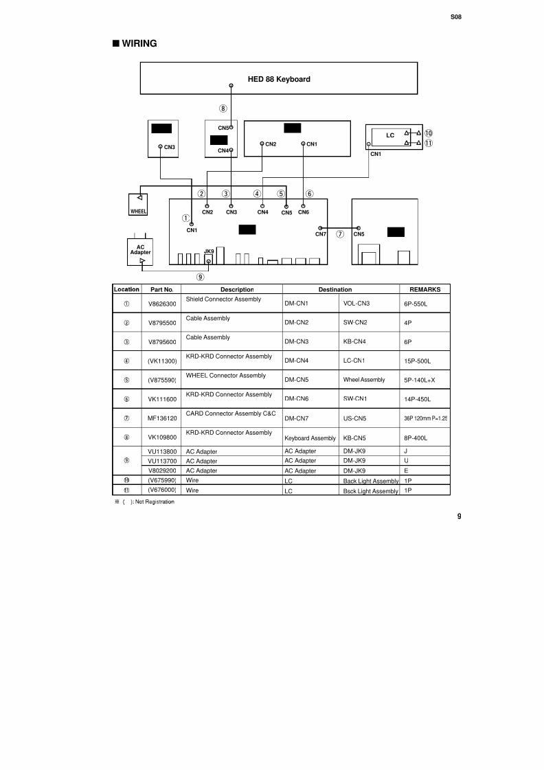
s WIRING
Part No. Description Destination REMARKS
SW
US
HED 88 Keyboard
CN4CN3CN2
JK9
CN1q
w e r t y
u
!0
!1LC
o
WHEEL
ACAdapter
DM
VOL
KBCN3 CN4
CN2
CN5
CN1
CN1
CN5CN7
CN6CN5
i
7/22/2019 Yamaha s08
http://slidepdf.com/reader/full/yamaha-s08 10/69
S08
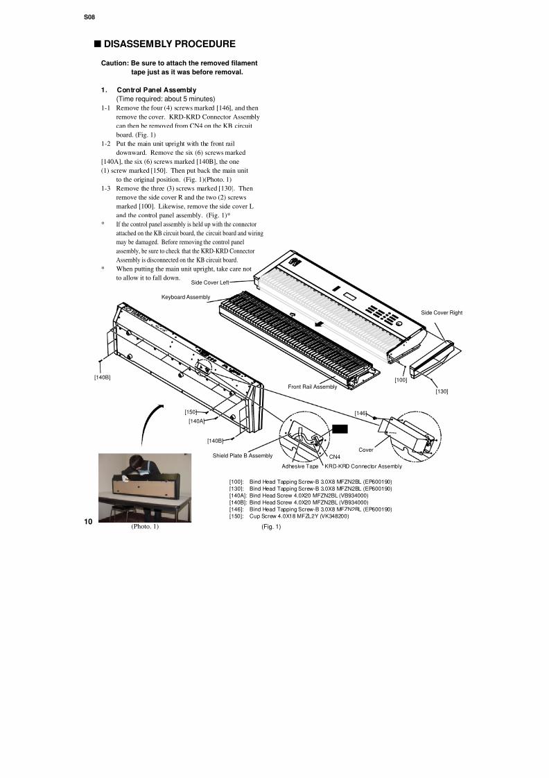
s DISASSEMBLY PROCEDURE
Caution: Be sure to attach the removed filament
tape just as it was before removal.
1. Control Panel Assembly
(Time required: about 5 minutes)
1-1 Remove the four (4) screws marked [146], and then
remove the cover. KRD-KRD Connector Assembly
can then be removed from CN4 on the KB circuit
board. (Fig. 1)
1-2 Put the main unit upright with the front rail
downward. Remove the six (6) screws marked
[140A], the six (6) screws marked [140B], the one
(1) screw marked [150]. Then put back the main unit
to the original position. (Fig. 1)(Photo. 1)
1-3 Remove the three (3) screws marked [130]. Then
remove the side cover R and the two (2) screws
marked [100]. Likewise, remove the side cover L
and the control panel assembly. (Fig. 1)*
* If the control panel assembly is held up with the connectorattached on the KB circuit board, the circuit board and wiring
may be damaged. Before removing the control panel
assembly, be sure to check that the KRD-KRD Connector
Assembly is disconnected on the KB circuit board.
* When putting the main unit upright, take care not
to allow it to fall down.Side Cover Left
K b d A bl
7/22/2019 Yamaha s08
http://slidepdf.com/reader/full/yamaha-s08 11/69
S08
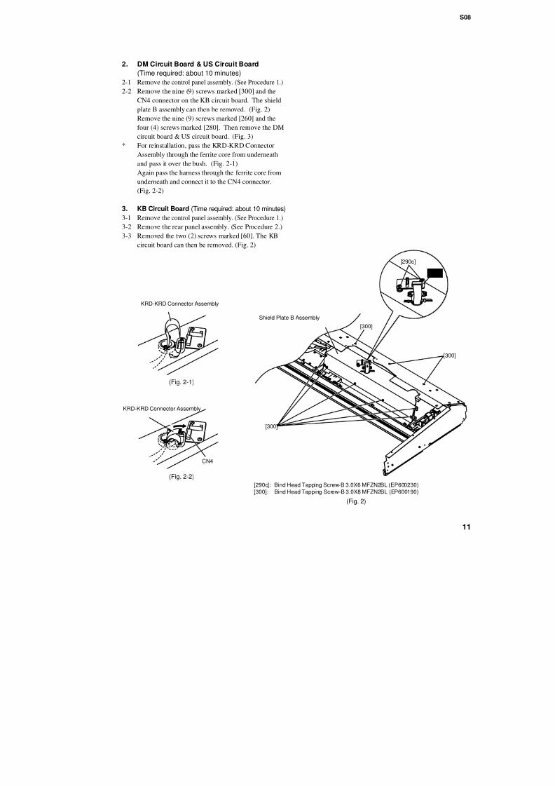
KB
[290c]
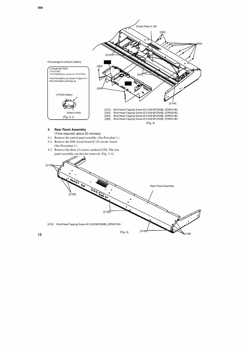
2. DM Circuit Board & US Circuit Board
(Time required: about 10 minutes)2-1 Remove the control panel assembly. (See Procedure 1.)
2-2 Remove the nine (9) screws marked [300] and the
CN4 connector on the KB circuit board. The shield
plate B assembly can then be removed. (Fig. 2)
Remove the nine (9) screws marked [260] and the
four (4) screws marked [280]. Then remove the DM
circuit board & US circuit board. (Fig. 3)
* For reinstallation, pass the KRD-KRD Connector
Assembly through the ferrite core from underneath
and pass it over the bush. (Fig. 2-1)
Again pass the harness through the ferrite core from
underneath and connect it to the CN4 connector.
(Fig. 2-2)
3. KB Circuit Board (Time required: about 10 minutes)
3-1 Remove the control panel assembly. (See Procedure 1.)
3-2 Remove the rear panel assembly. (See Procedure 2.)3-3 Removed the two (2) screws marked [60]. The KB
circuit board can then be removed. (Fig. 2)
7/22/2019 Yamaha s08
http://slidepdf.com/reader/full/yamaha-s08 12/69
S08
US
[280]
[260]
[210A]
[230]
[210A]
[260]
[280]
DM
Shield Plate A, DM
(Fig. 3)
[210]: Bind Head Tapping Screw-B 3.0X8 MFZN2BL (EP600190)
[230]: Bind Head Tapping Screw-B 3.0X6 MFZN2BL (EP600230)
[260]: Bind Head Tapping Screw-B 3.0X8 MFZN2BL (EP600190)
[280]: Bind Head Tapping Screw-B 3.0X8 MFZN2BL (EP600190)
4. Rear Panel Assembly
(Ti i d b i )
LITHIUM BATTERY
(VN103500)
VN103600(Battery holder for VN103500)
Exchange of a lithium battery
Battery holder
LITHIUM Battery
Push the battery as shown in figure 3-1, then the battery will pop up.
(Fig. 3-1)
7/22/2019 Yamaha s08
http://slidepdf.com/reader/full/yamaha-s08 13/69
S08
5. SW Circuit Board (Time required: about 25 minutes)
5-1 Remove the control panel assembly. (See Procedure 1.)
5-2 Remove the rear panel assembly. (See Procedure 4.)
5-3 Remove the nine (9) screws marked [60]. The SW
circuit board can then be removed.
* When installing SW circuit board, take care not to
pinch and damage the CN2 cable assembly. (Fig. 5-1)
6. VOL Circuit Board (Time required: about 25 minutes)
6-1 Remove the control panel assembly. (See Procedure 1.)
6-2 Remove the rear panel assembly. (See Procedure 4.)
6-3 Remove the four (4) screws marked [160].
* When installing the VOL circuit board, slide the
volume knob up and down with the VOL circuit
board in contact with the VOL circuit board fixture
and check that it moves smoothly. Then secure the
circuit board with the screws. (Fig. 5)
7. LCD Circuit Board (Time required: about 25 minutes)
7-1 Remove the control panel assembly. (See Procedure 1.)7-2 Remove the rear panel assembly. (See Procedure 4.)
7-3 Remove the six (6) screws marked [110]. The LC
circuit board can then be removed. (Fig. 5)
7/22/2019 Yamaha s08
http://slidepdf.com/reader/full/yamaha-s08 14/69
S08
[60]
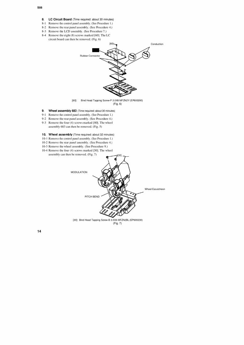
Rubber Connector
Conduction
LC
8. LC Circuit Board (Time required: about 30 minutes)
8-1 Remove the control panel assembly. (See Procedure 1.)
8-2 Remove the rear panel assembly. (See Procedure 4.)
8-3 Remove the LCD assembly. (See Procedure 7.)
8-4 Remove the eight (8) screws marked [60]. The LC
circuit board can then be removed. (Fig. 6)
9. Wheel assembly 683 (Time required: about 30 minutes)
9-1 Remove the control panel assembly. (See Procedure 1.)
9-2 Remove the rear panel assembly. (See Procedure 4.)
9-3 Remove the four (4) screws marked [80]. The wheel
assembly 683 can then be removed. (Fig. 5)
(Fig. 6)
[60]: Bind Head Tapping Screw-P 3.0X8 MFZN2Y (EP600280)
7/22/2019 Yamaha s08
http://slidepdf.com/reader/full/yamaha-s08 15/69
S08
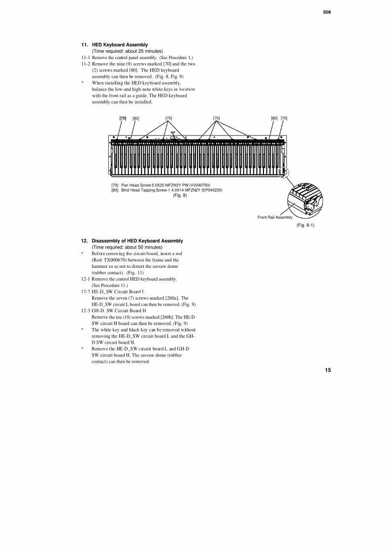
(Fig. 8)
[70]: Pan Head Screw 5.0X25 MFZN2Y PW (VV040700)
[80]: Bind Head Tapping Screw-1 4.0X14 MFZN2Y (EP040230)
[70] [70] [70] [70][80][70] [80]
11. HED Keyboard Assembly
(Time required: about 25 minutes)
11-1 Remove the control panel assembly. (See Procedure 1.)
11-2 Remove the nine (9) screws marked [70] and the two
(2) screws marked [80]. The HED keyboard
assembly can then be removed. (Fig. 8, Fig. 9)
* When installing the HED keyboard assembly,
balance the low-and high-note white keys in location
with the front rail as a guide. The HED keyboard
assembly can then be installed.
7/22/2019 Yamaha s08
http://slidepdf.com/reader/full/yamaha-s08 16/69
S08
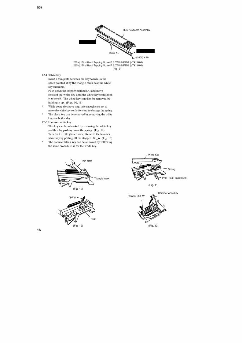
12-4 White key
Insert a thin plate between the keyboards (in the
space pointed at by the triangle mark near the white
key fulcrum).
Push down the stopper marked [A] and move
forward the white key until the white keyboard hook
is released. The white key can then be removed byholding it up. (Figs. 10, 11)
* While doing the above step, take enough care not to
move the white key so far forward to damage the spring.
* The black key can be removed by removing the white
keys on both sides.
12-5 Hammer white key
This key can be unhooked by removing the white key
[260a] X 7
[260b] X 10
[260a]: Bind Head Tapping Screw-P 3.0X10 MFZN2 (VT413400)
[260b]: Bind Head Tapping Screw-P 3.0X10 MFZN2 (VT413400)(Fig. 9)
HED Keyboard Assembly
HE-D_SW L
GH-D_SW H
7/22/2019 Yamaha s08
http://slidepdf.com/reader/full/yamaha-s08 17/69
S08
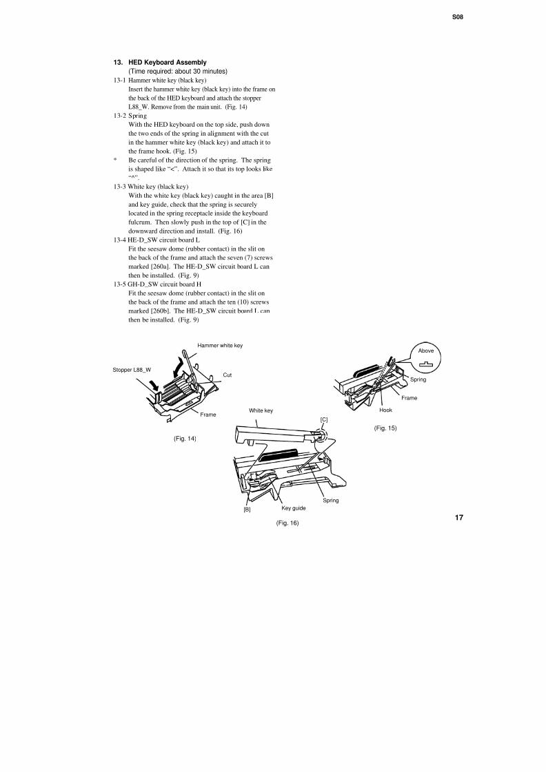
13. HED Keyboard Assembly
(Time required: about 30 minutes)
13-1 Hammer white key (black key)
Insert the hammer white key (black key) into the frame on
the back of the HED keyboard and attach the stopper
L88_W. Remove from the main unit. (Fig. 14)
13-2 Spring
With the HED keyboard on the top side, push down
the two ends of the spring in alignment with the cut
in the hammer white key (black key) and attach it to
the frame hook. (Fig. 15)
* Be careful of the direction of the spring. The spring
is shaped like “<”. Attach it so that its top looks like
“^”.
13-3 White key (black key)
With the white key (black key) caught in the area [B]
and key guide, check that the spring is securely
located in the spring receptacle inside the keyboard
fulcrum. Then slowly push in the top of [C] in thedownward direction and install. (Fig. 16)
13-4 HE-D_SW circuit board L
Fit the seesaw dome (rubber contact) in the slit on
the back of the frame and attach the seven (7) screws
marked [260a]. The HE-D_SW circuit board L can
then be installed. (Fig. 9)
13-5 GH-D_SW circuit board H
7/22/2019 Yamaha s08
http://slidepdf.com/reader/full/yamaha-s08 18/69
S08
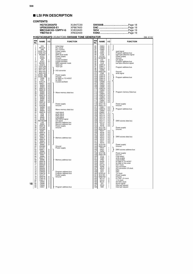
s LSI PIN DESCRIPTION
CONTENTS
HG73C205AFD XU947C00 SWX00B.................................... Page 18
UPD63200GS-E1 XP867A00 DAC ........................................... Page 19MBCG46183-129PFV-G XV833A00 SIO4 .......................................... Page 19YMZ702-D XR632A00 KSN2 ......................................... Page 19
PINNo.
NAME I/O FUNCTIONPINNo.
NAME I/O FUNCTION
1234
56789
10111213141516171819
20212223242526272829303132333435
ICNRFCLKI
TM2AVDD_PLL
AVSS_PLLMODE0VCC7GND8
XINXOUT
MODE1TEST0
TESTONAN0-P40AN1-P41AN2-P42AN3-P43
AVDD_ANAVSS_AN
TXD0TXD1EXCLKSMD11SMD4SMD3SMD12SMD10SMD5SMD2SMD13SMD9SMD6SMD1SMD14VCC35
III
I
IOIIIIIII
OOI
I/OI/OI/OI/OI/OI/OI/OI/OI/OI/OI/OI/O
Initial clearPLL ClockPLL ControlPower supply
GroundSWX dual modePower supplyGroundcrystal oscillatorcrystal oscillatorSWX separate modeTEST pinTEST pin
A/D converter
Power supplyGround
for MIDI or TO-HOSTfor MIDICrystal oscillator
Wave memory data bus
Power supply
85868788
8990919293949596979899100101102103
104105106107108109110111112113114115116117118119
CMA3CMA8CMA2CRD
CMA1CUB
VCC91GHND92
CS1CMA0CLB
CMA12CMA11CMA10CMA9
GND100CWE
CMA16CMA15
CMA14CMA13CMD8CMD7CMD9CMD6CMD10CMD5CMD11CMD4CMD12CMD3CMD13CMD2CMD14VCC119
OOOO
OO
OOOOOOO
OOO
OOI/OI/OI/OI/OI/OI/OI/OI/OI/OI/OI/OI/OI/O
read signal
Program address bushigh byte effective signalPower supplyGroundCS signalProgram address buslow byte effective signal
Program address bus
Groundwrite signal
Program address bus
Program memory Data bus
Power supply
q HG73C205AFD (XU947C00) SWX00B TONE GENERATOR DM: IC101
7/22/2019 Yamaha s08
http://slidepdf.com/reader/full/yamaha-s08 19/69
S08
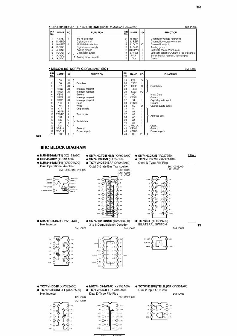
PINNo. NAME I/O FUNCTION
PINNo. NAME I/O FUNCTION
12345678
4/8FSD. GND16/8 BITD. VDDA. GNDR. OUTA. VDDA. VDD
I
I
O
4/8 Fs selectionDigital ground16 bit/8 bit selectionDigital power supplyAnalog groundChannel R output
Analog power supply
910111213141516
R. REFL. REFL. OUTA. GND
LRCX/WD
LR/RSISI/LSICLK
O
IIII
Channel R voltage referenceChannel L voltage referenceChannel L outputAnalog groundLeft/right check, Word clockLeft/right selection, Channel R series inputSeries input/Channel L series inputClock
UPD63200GS-E1 (XP867A00) DAC (Digital to Analog Converter) DM: IC018
PINNo.
NAME I/O FUNCTIONPINNo.
NAME I/O FUNCTION
123456
7891011121314151617
D5D6D7
/IRQ0 /IRQ1VSS6
/IRQ2 /IRQ3 /RD /WR /CE
/ASTBTESTI0
RX0TX0RX1TX1
I/OI/OI/OI/OI/O
I/OI/OIIIIIIOIO
Data bus
Interrupt requestInterrupt requestGround
Interrupt requestInterrupt requestReadWriteChip enable
Test mode
Serial data
252627282930
3132333435363738394041
TX31RX32TX32RX33TX33 /IC
VSS31XI
VSS33XOA0A1A2A3A4A5
CPUCLK
OIOI
I/OI
I
OIIIIIII
Serial data
Initial Clear
GroundCrystal quarts inputGroundCrystal quarts output
Address bus
Clock
MBCG46183-129PFV-G (XV833A00) SIO4 DM: IC030
7/22/2019 Yamaha s08
http://slidepdf.com/reader/full/yamaha-s08 20/69
7/22/2019 Yamaha s08
http://slidepdf.com/reader/full/yamaha-s08 21/69
S08
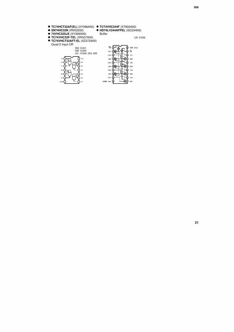
TC74HCT32AF(EL) (XY096A00)SN74HC32N (IR003250)
74VHC32SJX (XY306A00)TC74VHC32F-TEL (XR337A00)TC74VHCT32AFT-EL (XZ372A00)
Quad 2 Input ORDM: IC031SW: IC005US : IC002, 003, 008
TC74VHC244F (XT800A00)HD74LV244AFPEL (ISO24400)
BufferUS: IC006
1
2
3
1A
1Y
42A
52B
62Y
7GND
1B
14
13
12
Vcc
4A
11 4Y
10 3B
9 3A
8 3Y
4B
1
2
3
4
5
6
7
8 13
14
15
16
17
18
19
20
9
10 11
12
VDD (Vcc)
2G
1Y1
2A4
1Y2
2A3
1Y3
2A2
1Y4
2A1(GND) Vss
2Y1
1A4
2Y2
1A3
2Y3
1A2
2Y4
1A1
1G
S08
7/22/2019 Yamaha s08
http://slidepdf.com/reader/full/yamaha-s08 22/69
S08
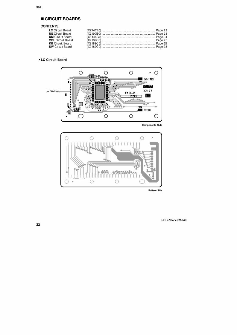
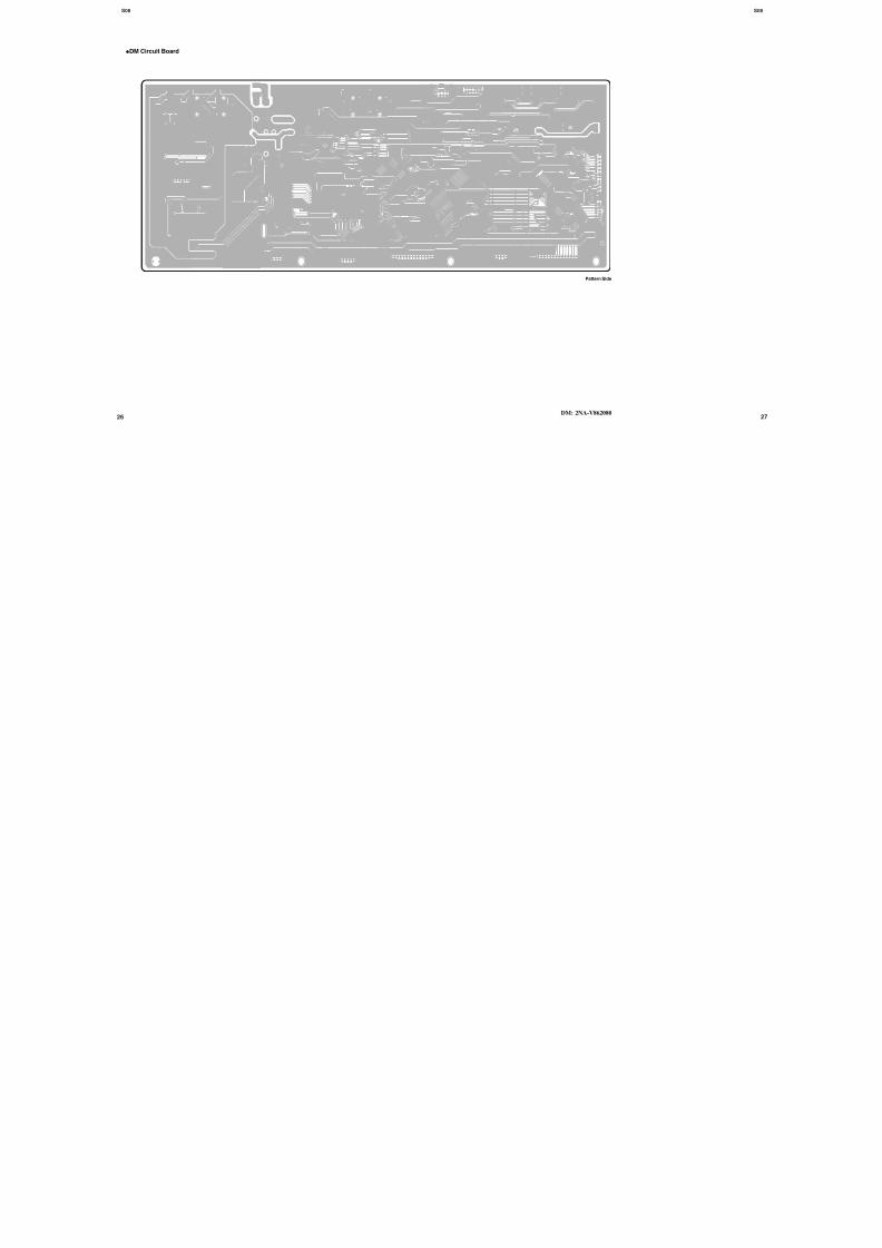
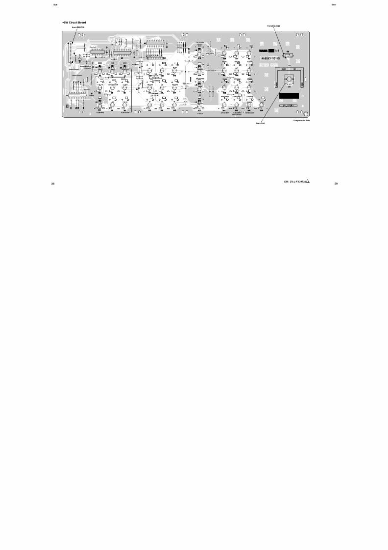
s CIRCUIT BOARDS
to DM-CN4
LC Circuit Board
Components Side
CONTENTS
LC Circuit Board (XZ147B0) ................................................................... Page 22
US Circuit Board (X2190B0) ................................................................... Page 23DM Circuit Board (XZ144G0) .................................................................. Page 24VOL Circuit Board (X2189C0) ................................................................... Page 25KB Circuit Board (X2189C0) ................................................................... Page 25SW Circuit Board (X2189C0) ................................................................... Page 28
S08
7/22/2019 Yamaha s08
http://slidepdf.com/reader/full/yamaha-s08 23/69
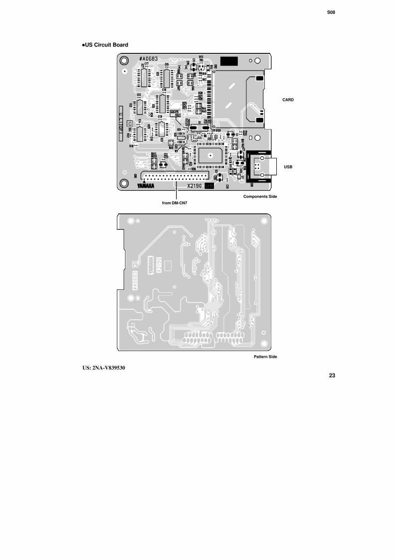
S08
Components Side
•US Circuit Board
from DM-CN7
USB
CARD
C
S08 S08
7/22/2019 Yamaha s08
http://slidepdf.com/reader/full/yamaha-s08 24/69
24 25
Components Side
G
RDC INSTANDBY/ONFOOT
CONTROLLER L/MONO
OUTPUT
PHONES
to SW-CN2
not installed
Overcurrent protection
Components Side
Components Side
•VOL Circuit Board •KB Circuit Board
to HE-D_SW L
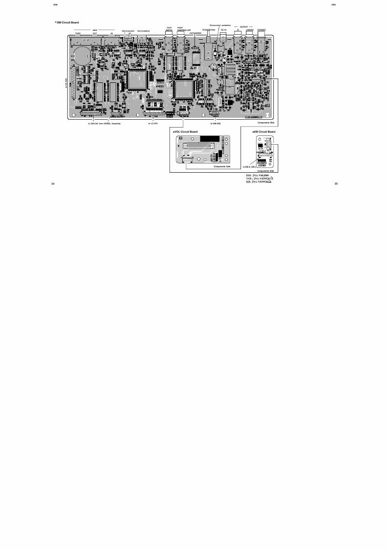
DM Circuit Board
THRU OUT
MIDI
IN
FOOT
SWITCH
to SW-CN1
t o
U S - C N 5
from WHEEL Assembly to LC-CN1
Not Installed Not Installed
DM: 2NA-V862080
VOL: 2NA-V839520 2
KB: 2NA-V839520 2
S08 S08
7/22/2019 Yamaha s08
http://slidepdf.com/reader/full/yamaha-s08 25/69
26 27DM: 2NA-V862080
Pattern Side
•DM Circuit Board
S08 S08
7/22/2019 Yamaha s08
http://slidepdf.com/reader/full/yamaha-s08 26/69
28 29
Components Side
SW: 2NA-V839520 2
CATEGORYSEACH
PRESET
DRUM/PIPE
USER
SE
GM2/XG
OTHER
7 8 9
4 5 6
1 2 3
0 - ENTER EXIT
PIANO ORGAN GUITAR
BASS STRINGS BRASS
R EED/PIPE SYN LEA D SYN PAD
SYN COMP CHROMTICPERCUSSION
KEYBOARD
from DM-CN2
Data Dial
•SW Circuit Board
COCOMMON
VOICE MULTI SEQ PLAY
DEMO
U TILITY C ON TR OLLER C AR D
EDIT
COMPARE PLAY/STOP
JOB STORE
+- MUTE
DEC/NO INC/YES
from DM-CN6
S08
7/22/2019 Yamaha s08
http://slidepdf.com/reader/full/yamaha-s08 27/69
S08
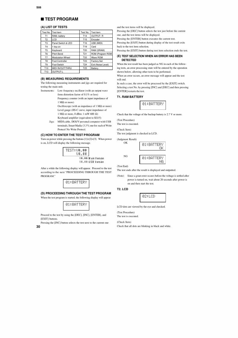
s TEST PROGRAM
(A) LIST OF TESTS
Test No.
T1
T2
T3
T4
T5
T6
T7
T8
T9
T10
T13
Test No.
T14
T15
T16
T19
T20
T21
T22
T23
T24
T25
Test item
RAM, battery
LCD
Panel Switch & LED
1 key on
Keyboard
Pitch Bend
Modulation Wheel
Foot Controller
Foot Switch
MIDI IN/OUT/THRU
OUTPUT-L
Test item
OUTPUT- R
Encoder
USB (MIDI)
Card
RAM (SRAM)
ROM (Program ROM)
Wave ROM
Factory Set
Exit (Noise Level)
Battery
(B) MEASURING REQUIREMENTS
The following measuring instruments and jigs are required for
testing the main unit.
Instruments: Low-frequency oscillator (with an output wave
form distortion factor of 0.1% or less)
Frequency counter (with an input impedance of 1 MΩ or more)
Oscilloscope (with an impedance of 1 MΩ or more)
Level gauge (JIS-C curve, input impedance of
1 MΩ or more, 0 dBm: 1 mW 600 Ω)
Keyboard amplifier (equivalent to KS15)
Jigs: MIDI cable, DOS/V personal computer with USB
terminals, Smart Madia (3.3 V, one for each of Write
and the test items will be displayed.
Pressing the [DEC] button selects the test just before the current
one, and the test items will be displayed.
Pressing the [ENTER] button executes the current test.
Pressing the [EXIT] button during display of the test result exits
back to the test item selection.
Pressing the [EXIT] button during test item selection ends the test.
(E) TEST SELECTION WHEN AN ERROR HAS BEEN
DETECTED
When the test result has been judged as NG in each of the follow-
ing tests, an error processing state will be entered by the operation
shown below, allowing other tests to be performed.
When an error occurs, an error message will appear and the test
will end.
In such a case, the error will be processed by the [EXIT] switch.
Selecting a test No. by pressing [INC] and [DEC] and then pressing
[ENTER] restarts the test.
T1. RAM BATTERY
01:BATTERY
Check that the voltage of the backup battery is 2.7 V or more.
(Test Procedure)
The test is executed.
S08
7/22/2019 Yamaha s08
http://slidepdf.com/reader/full/yamaha-s08 28/69
(Judgment Result)
None
(Test End)
Pressing [EXIT] ends the test.
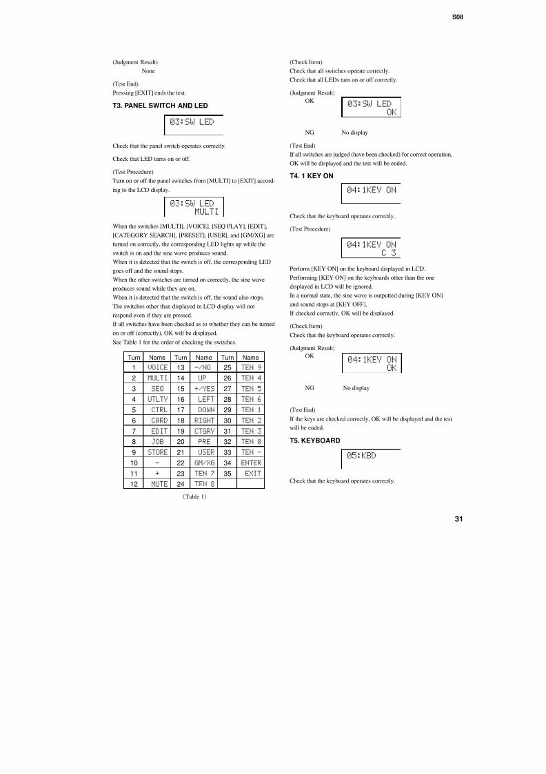
T3. PANEL SWITCH AND LED
03:SW LED
Check that the panel switch operates correctly.
Check that LED turns on or off.
(Test Procedure)
Turn on or off the panel switches from [MULTI] to [EXIT] accord-
ing to the LCD display.
03:SW LED
MULTI
When the switches [MULTI], [VOICE], [SEQ PLAY], [EDIT],
[CATEGORY SEARCH], [PRESET], [USER], and [GM/XG] are
turned on correctly, the corresponding LED lights up while the
switch is on and the sine wave produces sound.
When it is detected that the switch is off, the corresponding LED
goes off and the sound stops.
When the other switches are turned on correctly, the sine wave
produces sound while they are on.
(Check Item)
Check that all switches operate correctly.
Check that all LEDs turn on or off correctly.
(Judgment Result)
OK03:SW LED
OK
NG No display
(Test End)
If all switches are judged (have been checked) for correct operation,
OK will be displayed and the test will be ended.
T4. 1 KEY ON
04:1KEY ON
Check that the keyboard operates correctly.
(Test Procedure)
04:1KEY ON
C 3
Perform [KEY ON] on the keyboard displayed in LCD.
Performing [KEY ON] on the keyboards other than the one
displayed in LCD will be ignored.
In a normal state the sine wave is outputted during [KEY ON]
S08
7/22/2019 Yamaha s08
http://slidepdf.com/reader/full/yamaha-s08 29/69
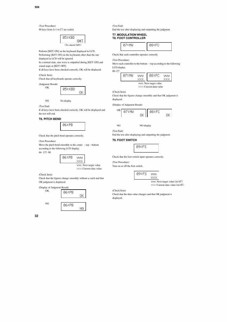
(Test Procedure)
88 keys from A-1 to C7 are scaled.
05:KBD
G#3
(To check G#3)
Perform [KEY ON] on the keyboard displayed in LCD.
Performing [KEY ON] on the keyboards other than the one
displayed in LCD will be ignored.
In a normal state, sine wave is outputted during [KEY ON] andsound stops at [KEY OFF].
If all keys have been checked correctly, OK will be displayed.
(Check Item)
Check that all keyboards operate correctly.
(Judgment Result)
OK
05:KBD
OK
NG No display
(Test End)
If all keys have been checked correctly, OK will be displayed and
the test will end.
T6. PITCH BEND
(Test End)
End the test after displaying and outputting the judgment.
T7. MODULATION WHEELT8. FOOT CONTROLLER
07:MW 08:FC
Check that each controller operates correctly.
(Test Procedure)
Move each controller to the bottom – top according to the following
LCD display.
00-127
07:MW yyy
xxx
08:FC yyy
xxx
yyy: Next target value
xxx:Current data value
(Check Item)
Check that the figures change smoothly and that OK judgment is
displayed.
(Display of Judgment Result)
OK
07:MW
OK
08:FC
OK
S08
7/22/2019 Yamaha s08
http://slidepdf.com/reader/full/yamaha-s08 30/69
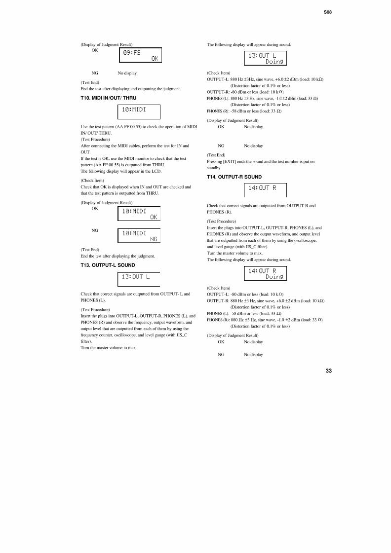
(Display of Judgment Result)
OK
09:FS
OK
NG No display
(Test End)
End the test after displaying and outputting the judgment.
T10. MIDI IN/OUT/ THRU
10:MIDI
Use the test pattern (AA FF 00 55) to check the operation of MIDI
IN/ OUT/ THRU.
(Test Procedure)
After connecting the MIDI cables, perform the test for IN and
OUT.
If the test is OK, use the MIDI monitor to check that the test
pattern (AA FF 00 55) is outputted from THRU.
The following display will appear in the LCD.
(Check Item)
Check that OK is displayed when IN and OUT are checked and
that the test pattern is outputted from THRU.
(Display of Judgment Result)
OK10:MIDI
The following display will appear during sound.
13:OUT LDoing
(Check Item)
OUTPUT-L: 880 Hz ±3Hz, sine wave, +6.0 ±2 dBm (load: 10 k Ω)
(Distortion factor of 0.1% or less)
OUTPUT-R: -80 dBm or less (load: 10 k Ω)
PHONES (L): 880 Hz ±3 Hz, sine wave, -1.0 ±2 dBm (load: 33 Ω)
(Distortion factor of 0.1% or less)
PHONES (R): -58 dBm or less (load: 33Ω)
(Display of Judgment Result)
OK No display
NG No display
(Test End)
Pressing [EXIT] ends the sound and the test number is put onstandby.
T14. OUTPUT-R SOUND
14:OUT R
Check that correct signals are outputted from OUTPUT-R and
S08
7/22/2019 Yamaha s08
http://slidepdf.com/reader/full/yamaha-s08 31/69
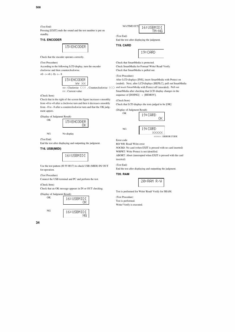
(Test End)
Pressing [EXIT] ends the sound and the test number is put on
standby.
T15. ENCODER
15:ENCODER
Check that the encoder operates correctly.
(Test Procedure)
According to the following LCD display, turn the encoder
clockwise and then counterclockwise.
+0 - > +8 (- 0)- > - 8
15:ENCODER
yy xx
yy : Clockwise(>>), Counterclockwise(<<)
xx : Current value
(Check Item)Check that in the right of the screen the figure increases smoothly
from +0 to +8 after a clockwise turn and then it decreases smoothly
from –0 to –8 after a counterclockwise turn and that the OK judg-
ment appers.
(Display of Judgment Result)
OK15:ENCODER
OK
NG16:USBMIDI
TM-NG
(Test End)
End the test after displaying the judgment.
T19. CARD
19:CARD
Check that SmartMedia is protected.
Check SmartMedia for Format/ Write/ Read/ Verify.
Check that SmartMedia is pulled out.
(Test Procedure)
After LCD displays [INS], insert SmartMedia with Protect on
(sealed). Next, after LCD displays [REPLC], pull out SmartMedia
and insert SmartMedia with Protect off (unsealed). Pull out
SmartMedia after checking that LCD display changes in the
sequence of [DOING] [REMOV].
(Check Item)
Check that LCD displays the tests judged to be [OK]
(Display of Judgment Result)
OK19:CARD
OK
(TIME OUT)
S08
7/22/2019 Yamaha s08
http://slidepdf.com/reader/full/yamaha-s08 32/69
(Check Item)
The test result is checked in LCD.
(Display of Judgment Result)
OK
20:RAM R/W
OK
NG20:RAM R/W
NG
(Test End)
End the test after displaying and outputting the judgment.
(Note) All data on RAM is stored. Data will be evacuated
immediately before verifying check and be stored
immediately after it in repeated sequence.
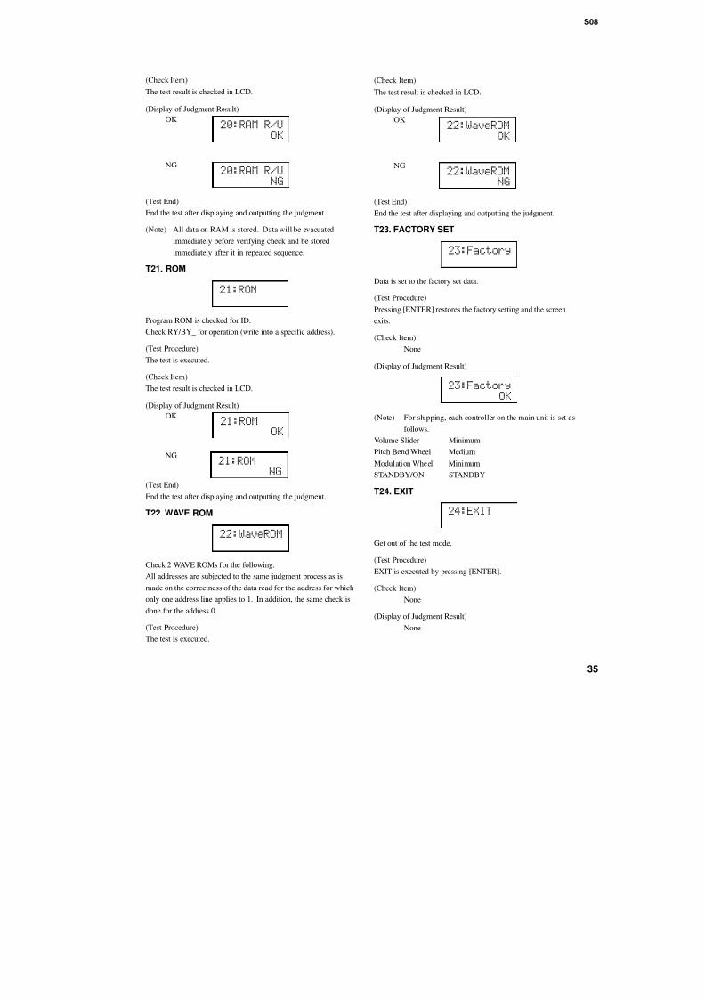
T21. ROM
21:ROM
Program ROM is checked for ID.
Check RY/BY_ for operation (write into a specific address).
(Test Procedure)
The test is executed.
(Check Item)
(Check Item)
The test result is checked in LCD.
(Display of Judgment Result)
OK
22:WaveROM
OK
NG
22:WaveROM
NG
(Test End)
End the test after displaying and outputting the judgment.
T23. FACTORY SET
23:Factory
Data is set to the factory set data.
(Test Procedure)
Pressing [ENTER] restores the factory setting and the screen
exits.
(Check Item)
None
(Display of Judgment Result)
S08

7/22/2019 Yamaha s08
http://slidepdf.com/reader/full/yamaha-s08 33/69
(Test End)
EXIT is executed by pressing [ENTER].
(Note) Getting out of the test mode is followed by the same
sequence as when power is turned on. Also check that
the noise level meets the following conditions when
none of the note-on steps are made in normal mode after
a test subsequent to the factory set.
Measure using the level gauge (with JIF-C filter).
OUTPUT-L- - - - - - - - - - > -87 dBm or less (load: 10 k Ω)
OUTPUT-R- - - - - - - - - - > -87 dBm or less (load: 10 k Ω
)PHONES-L- - - - - - - - - - > -94 dBm or less (load: 33 Ω)
PHONES-R- - - - - - - - - - > -94 dBm or less (load: 33 Ω)
Power consumption: Measured at DC IN terminal
230 mA ± 10 %
T25. BATTERY
Perform the test 30 seconds before power is on or after power is
off.
Check the voltage between the positive terminal of C154 and
DGND.
(Test Procedure)
Perform measurement of the voltage between the positive
terminal of C154 and DGND using an instrument with an
impedance of 1M ohms or more.
(Check Item)
S08

7/22/2019 Yamaha s08
http://slidepdf.com/reader/full/yamaha-s08 34/69
S08

7/22/2019 Yamaha s08
http://slidepdf.com/reader/full/yamaha-s08 35/69
S08

7/22/2019 Yamaha s08
http://slidepdf.com/reader/full/yamaha-s08 36/69
S08

7/22/2019 Yamaha s08
http://slidepdf.com/reader/full/yamaha-s08 37/69
S08

7/22/2019 Yamaha s08
http://slidepdf.com/reader/full/yamaha-s08 38/69
S08
7/22/2019 Yamaha s08
http://slidepdf.com/reader/full/yamaha-s08 39/69
S08
7/22/2019 Yamaha s08
http://slidepdf.com/reader/full/yamaha-s08 40/69
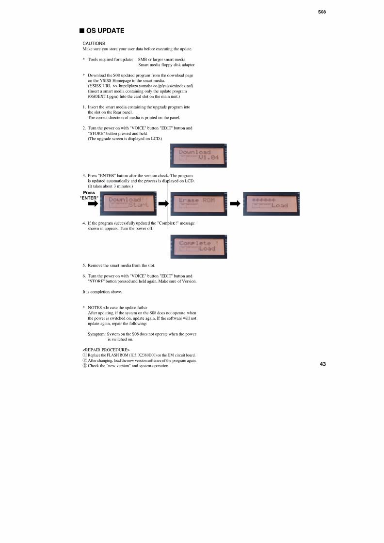
s OS UPDATE
Press
"ENTER"
CAUTIONSMake sure you store your user data before executing the update.
* Tools required for update: 8MB or larger smart media
Smart media floppy disk adaptor
* Download the S08 updated program from the download page
on the YSISS Homepage to the smart media.
(YSISS URL >> http://plaza.yamaha.co.jp/ysiss/exindex.nsf)
(Insert a smart media containing only the update program
(0683EXT1.pgm) Into the card slot on the main unit.)
1. Insert the smart media containing the upgrade program intothe slot on the Rear panel.
The correct direction of media is printed on the panel.
2. Turn the power on with "VOICE" button "EDIT" button and
"STORE" button pressed and held.
(The upgrade screen is displayed on LCD.)
3. Press "ENTER" button after the version check. The program
is updated automatically and the process is displayed on LCD.
(It takes about 3 minutes.)
S08
7/22/2019 Yamaha s08
http://slidepdf.com/reader/full/yamaha-s08 41/69
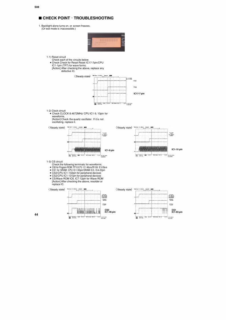
IC17-7 pin
Steady state
1. Backlight alone turns on, or screen freezes.(Or test mode is inaccessible.)
1-1) Reset circuitCheck each of the circuits below.
• Check Check for Reset Reset IC17-7pin/CPUIC1-1pin (TP7) for wave forms.[Action] After checking the above, replace any
defective IC.
1-2) Clock circuit
• Check CLOCK 8.4672MHz/ CPU IC1-9, 10pin forwaveforms.[Action] Check the quartz oscillator. If it is notoscillating replace it
s CHECK POINT・TROUBLESHOOTING
S08
7/22/2019 Yamaha s08
http://slidepdf.com/reader/full/yamaha-s08 42/69
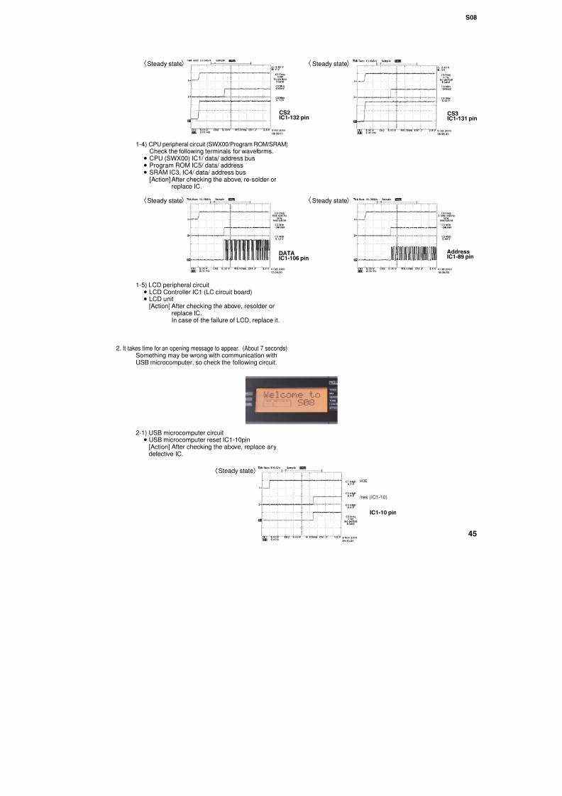
CS3IC1-131 pin
CS2IC1-132 pin
DATAIC1-106 pin
AddressIC1-89 pin
Steady state Steady state
Steady state Steady state
1-4) CPU peripheral circuit (SWX00/Program ROM/SRAM)Check the following terminals for waveforms.
• CPU (SWX00) IC1/ data/ address bus• Program ROM IC5/ data/ address
• SRAM IC3, IC4/ data/ address bus[Action] After checking the above, re-solder or
replace IC.
1-5) LCD peripheral circuit
• LCD Controller IC1 (LC circuit board)
• LCD unit[A ti ] Aft h ki th b ld
S08
7/22/2019 Yamaha s08
http://slidepdf.com/reader/full/yamaha-s08 43/69
IC1-14 pin
Steady state
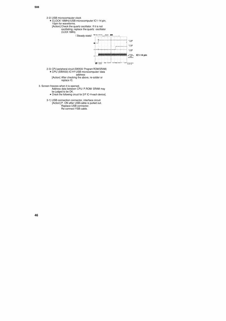
2-2) USB microcomputer clock
• CLOCK 16MHz/USB microcomputer IC1-14 pin,10pin for waveforms.[Action] Check the quartz oscillator. If it is not
oscillating, replace the quartz oscillator(CLOCK 16MHz).
2-3) CPU peripheral circuit (SWX00/ Program ROM/SRAM)
• CPU (SWX00) IC1 USB microcomputer/ dataaddress
[Action] After checking the above, re-solder orreplace IC.
3. Screen freezes when it is opened.
Address data between CPU/ P.ROM/ SRAM maybe judged to be OK.
• Check the following circuit for [I/F IC each device].
3-1) USB connection connector, interface circuit[Action] P. ON after USB cable is pulled out.
Replace USB connector.Re-connect YSB cable.
S08

7/22/2019 Yamaha s08
http://slidepdf.com/reader/full/yamaha-s08 44/69
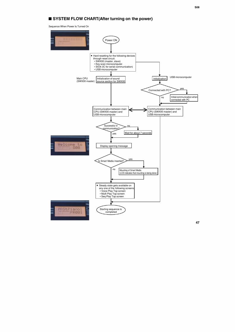
Power ON
Initialization of soundsource section for SWX00
Communication between mainCPU (SWX00 master) andUSB microcomputer
Successful in no
Main CPU(SWX00 master)
Initialization
Connected with PC?yes
no
USB microcomputer
Initial communication whenconnected with PC
Communication between mainCPU (SWX00 master) andUSB microcomputer
Sequence When Power Is Turned On
• Hard resetting for the following devicesthrough reset circuit.• SWX00 (master, slave)• Key scan microcomputer
• SIO4 (IC for serial communication)• USB microcomputer
s SYSTEM FLOW CHART(After turning on the power)
S08
7/22/2019 Yamaha s08
http://slidepdf.com/reader/full/yamaha-s08 45/69
S08

7/22/2019 Yamaha s08
http://slidepdf.com/reader/full/yamaha-s08 46/69
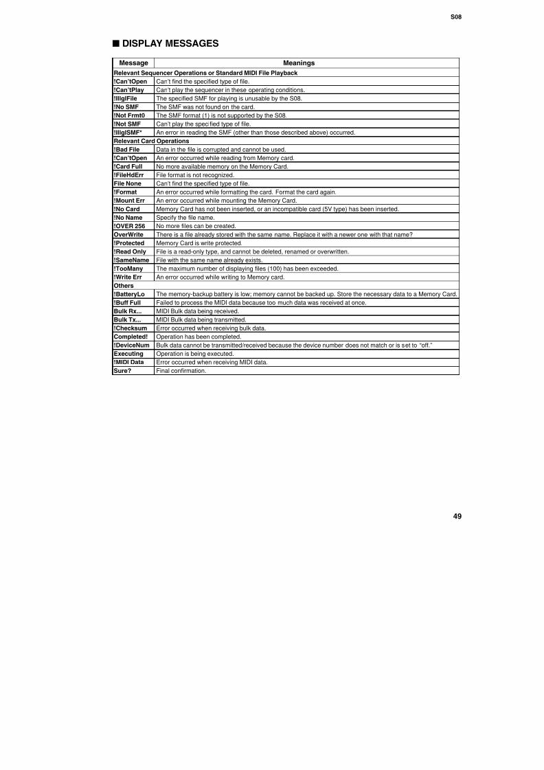
s DISPLAY MESSAGES
Relevant Sequencer Operations or Standard MIDI File Playback
!Can’tOpen!Can’tPlay
!IllglFile
!No SMF
!Not Frmt0
!Not SMF
!IllglSMF*
Relevant Card Operations
!Bad File
!Can’tOpen
!Card Full
!FileHdErr
File None
!Format
!Mount Err
!No Card
!No Name
!OVER 256OverWrite
!Protected
!Read Only
!SameName
!TooMany
!Write Err
Others
!BatteryLo
Can’t find the specified type of file.Can’t play the sequencer in these operating conditions.
The specified SMF for playing is unusable by the S08.
The SMF was not found on the card.
The SMF format (1) is not supported by the S08.
Can’t play the specified type of file.
An error in reading the SMF (other than those described above) occurred.
Data in the file is corrupted and cannot be used.
An error occurred while reading from Memory card.
No more available memory on the Memory Card.
File format is not recognized.
Can’t find the specified type of file.
An error occurred while formatting the card. Format the card again.
An error occurred while mounting the Memory Card.
Memory Card has not been inserted, or an incompatible card (5V type) has been inserted.
Specify the file name.
No more files can be created.There is a file already stored with the same name. Replace it with a newer one with that name?
Memory Card is write protected.
File is a read-only type, and cannot be deleted, renamed or overwritten.
File with the same name already exists.
The maximum number of displaying files (100) has been exceeded.
An error occurred while writing to Memory card.
The memory-backup battery is low; memory cannot be backed up Store the necessary data to a Memory Card
MeaningsMessage
S08
7/22/2019 Yamaha s08
http://slidepdf.com/reader/full/yamaha-s08 47/69
S08
7/22/2019 Yamaha s08
http://slidepdf.com/reader/full/yamaha-s08 48/69
S08
7/22/2019 Yamaha s08
http://slidepdf.com/reader/full/yamaha-s08 49/69
7/22/2019 Yamaha s08
http://slidepdf.com/reader/full/yamaha-s08 50/69
PARTS LISTs CONTENTSOVERALL ASSEMBLY ............................................................... 2
CONTROL PANEL ASSEMBLY ................................................. 4SW CIRCUIT BORAD ASSEMBLY ............................................ 6HED KEYBOARD ASSEMBLY ................................................... 7LCD ASSEMBLY ........................................................................ 8WHEEL ASSEMBLY 683 ...........................................................9WHEEL ASSEMBLY .................................................................. 9ELECTRICAL PARTS .............................................................. 10
Notes: DESTINATION ABBREVIATIONS
S08
7/22/2019 Yamaha s08
http://slidepdf.com/reader/full/yamaha-s08 51/69
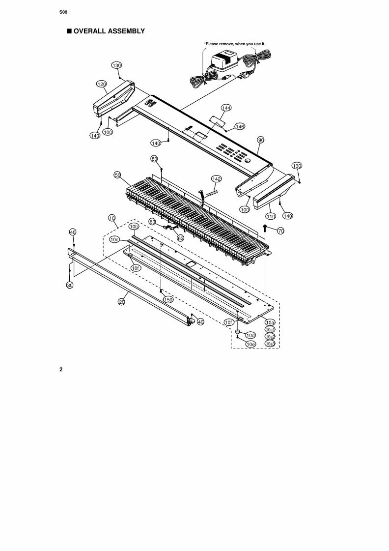
s OVERALL ASSEMBLY
90
80
144
146
142
120
130
130
140
140
50
100
100
*Please remove, when you use it.
S08
7/22/2019 Yamaha s08
http://slidepdf.com/reader/full/yamaha-s08 52/69
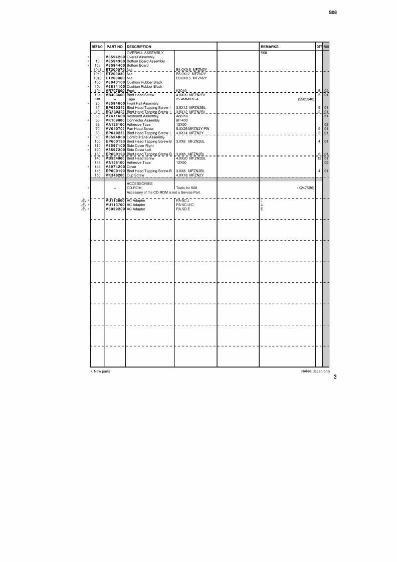
OVERALL ASSEMBLYOverall Assembly
Bottom Board AssemblyBottom BoardNutNutNutCushion Rubber BlackCushion Rubber BlackFootBind Head ScrewTapeFront Rail AssemblyBind Head Tapping Screw-1
Bind Head Tapping Screw-1Keyboard AssemblyConnector AssemblyAdhesive TapePan Head ScrewBind Head Tapping Screw-1Control Panel AssemblyBind Head Tapping Screw-BSide Cover RightSide Cover LeftBind Head Tapping Screw-BBind Head ScrewAdhesive Tape
CoverBind Head Tapping Screw-BCup Screw
ACCESSORIESCD-ROM
AC AdapterAC AdapterAC Adapter
0201
01
0151
030101
01
010103
01
55
5
2
92
4
612
4
S08
(2205340)
(X2475B0)
JUE
B4.0X9.5 MFZN2YB5.0X12 MFZN2YB3.0X9.5 MFZN2Y
K30194.0X20 MFZN2BL25.4MMX16.4
3.5X12 MFZN2BL
3.5X12 MFZN2BLA88 K68P-40012X505.0X25 MFZN2Y PW4.0X14 MFZN2Y
3.0X8 MFZN2BL
3.0X8 MFZN2BL4.0X20 MFZN2BL12X50
3.0X8 MFZN2BL4.0X18 MFZN2Y
Tools for S08
PA-5C JPA-5C U/CPA-5D E
V8594200
V8594300V8594400ET200070ET200030ET200080V8040100V8814100VR707800VB403600
--V8594600EP030340
EG330320V7411600VK109800VA126100VV040700EP040230V8594800EP600190V8597100V8597200EP600190VB934000VA126100
V8974200EP600190VK348200
--
VU113800VU113700V8029200
1010a10a110a210a310b10c10d10e10f2030
40506062708090
100110120130140142
144146150
∗
∗
∗
∗
∗
∗
∗
∗
∗
∗
∗
∗
∗
∗
DESCRIPTIONREF NO. PART NO. REMARKS QTY RANK
Accessory of the CD-ROM is not a Service Part.
S08
7/22/2019 Yamaha s08
http://slidepdf.com/reader/full/yamaha-s08 53/69
180
10
70
80
30 90
6050
170a
270b
270c270d
290a
170b
170c
180c
360
380
370
170
100
110
120
130
162160
160140
150310
162
190220
250
260
262
270
240
252
230
230
190
180a
180b
20
40
260
390
s CONTROL PANEL ASSEMBLY
S08
7/22/2019 Yamaha s08
http://slidepdf.com/reader/full/yamaha-s08 54/69
04
01
01
01
0301
030101
01
01
01
010101
01
03
2
9
4
6
43
2
2
6
392
15
5
2
S08
(X2189B0)
(X2189B0)
(V859950)
(XZ144G0)
EX55X20
SW3.0X8 MFZN2BL
3.0X8 MFZN2BL
S-34Z3.0X8 MFZN2BLVOL
KR-KR 6P 550L1S-34B3.0X8 MFZN2BL3.0X6 MFZN2BL
RightRight3.0X6 MFZN2BL
LEFTLEFT3.0X6 MFZN2BL
3.0X6 MFZN2BL
1.6 C3.0X8 MFZN2BLSB-19093.0X8 MFZN2BL0.8 C
3.0X6 MFZN2BLDMS-34Z6P
CONTROL PANEL ASSEMBLYControl Panel Assembly
Control PanelSRV EscutcheonTapeDust-Proof ClothCircuit Board AssemblyBind Head Tapping Screw-BWheel AssemblyBind Head Tapping Screw-BLCD AssemblyCord BinderBind Head Tapping Screw-BCircuit Board
Connector AssemblyAngle, VOLCord BinderBind Head Tapping Screw-BBind Head Tapping Screw-BAngle R AssemblySide AngelEnd BlockBind Head Tapping Screw-BAngle L AssemblySide AngleEnd BlockBind Head Tapping Screw-B
Bind Head Tapping Screw-BRear Panel AssemblyRear PanelAngle Bracket, PanelBind Head Tapping Screw-BBushingBind Head Tapping Screw-BShield Plate A, DMBind Head Tapping Screw-BCircuit BoardCord BinderCable Assembly
V8594800
V8594900V2772900VU354700VH810100V8597600EP600190V8600800EP600190V8598100CB829850EP600190V8626100
V8626300V8598300CB829850EP600190EP600230V8598400V8598600V8598800EP600230V8598500V8598700V8598900EP600230
EP600230V8599000V8599100V8599300EP600190V3079400EP600190
--EP600230V8620800CB829850V8795600
102030405060708090
100110120
130140150160162170
170a170b170c180
180a180b180c
190200
200a200b200c200d210220230240250252
∗
∗
∗
∗
∗
∗
∗
∗
∗
∗
∗
∗
∗
∗
∗
∗
∗
∗
∗
DESCRIPTIONREF NO. PART NO. REMARKS QTY RANK
S08
7/22/2019 Yamaha s08
http://slidepdf.com/reader/full/yamaha-s08 55/69
s SW CIRCUIT BORAD ASSEMBLY
130
100
110 12090 10 40 20 70
80507030 60 30
S08
s HED KEYBOARD ASSEMBLY

7/22/2019 Yamaha s08
http://slidepdf.com/reader/full/yamaha-s08 56/69
s HED KEYBOARD ASSEMBLY
110
100 280270
200
224230
260310
300
190240
220222
210
10
6070
80
90
2030
4050
S08
s LCD ASSEMBLY

7/22/2019 Yamaha s08
http://slidepdf.com/reader/full/yamaha-s08 57/69
s LCD ASSEMBLY
4040
30
80
70
20
10
S08
sWHEEL ASSEMBLY 683

7/22/2019 Yamaha s08
http://slidepdf.com/reader/full/yamaha-s08 58/69
sWHEEL ASSEMBLY 683
sWHEEL ASSEMBLY
10
20
30
•PITCH BEND(ピッチベンド) •MODULATION(モジュレ− ション)
W20 W20
014
S08
3.0X6 MFZN2BL
WHEEL ASSEMBLYWheel AssemblyWheel EscutcheonWheel AssemblyBind Head Tapping Screw-B
V8600800V8598000V8597900EP600230
102030
∗
∗
∗
DESCRIPTIONREF NO. PART NO. REMARKS QTY RANK
S08
s ELECTRICAL PARTS

7/22/2019 Yamaha s08
http://slidepdf.com/reader/full/yamaha-s08 59/69
131008
010301010101010101010101010101
010101010101010101010101
S08(XZ144G0)
(XT241A0)(XT240A0)(XZ147B0)(X2189B0)(X2189B0)(X2189B0)(X2190B0)
(XZ144G0)(V776760)
DM
GH-D_SW HHE-D_SW LLCSWVOLKBUS
DM
3.0X6 MFZN2BLCR20320.0100 50V K2200P 50V K2200P 50V K0.0100 50V K470.00 25.0V100.00 25.0V470.00 25.0V
220 16V UUR1C2100 16V47 16V
1000P 50V K1000P 50V K
47 16V
22 16V220 16V UUR1C222 16V
220 16V UUR1C2470P 50V J470P 50V J10 16V
100P 50V J100P 50V J3.3 35V27P 50V J27P 50V J
ELECTRICAL PARTSCircuit Board
Circuit BoardCircuit BoardCircuit BoardCircuit BoardCircuit BoardCircuit BoardCircuit Board
Circuit BoardHolder, JackBind Head ScrewBattery HolderCeramic Capacitor-B (chip)Ceramic Capacitor-B (chip)Ceramic Capacitor-B (chip)Ceramic Capacitor-B (chip)Electrolytic Cap.-RSElectrolytic Cap.Electrolytic Cap.-RSElectrolytic Cap. (chip)Electrolytic Cap. (chip)Electrolytic Cap. (chip)Ceramic Capacitor-B (chip)Ceramic Capacitor-B (chip)Electrolytic Cap. (chip)
Electrolytic Cap. (chip)Electrolytic Cap. (chip)Electrolytic Cap. (chip)Electrolytic Cap. (chip)Ceramic Capacitor-SL(chip)Ceramic Capacitor-SL(chip)Electrolytic Cap. (chip)Ceramic Capacitor-SL(chip)Ceramic Capacitor-SL(chip)Electrolytic Cap. (chip)Ceramic Capacitor-CH(chip)Ceramic Capacitor-CH(chip)
V8620800
VZ705300V7411800V6760100V8626000V8626100V8893800V8395300
V8620800--
EG330360VN103600US064100US063220US063220US064100VH340500UI548100VH340500UF138220UF038100UF037470US063100US063100UF037470
UF037220UF138220UF037220UF138220US062470US062470UF037100US062100US062100UF056330US061270US061270
2040
BT001C0001C0002C0003C0004C0005C0006C0007C0008C0010C0011C0012C0013C0014
C0015C0016C0017C0018C0019C0020C0021C0022C0023C0024C0025C0026
∗
∗
∗
∗
∗
∗
DESCRIPTIONREF NO. PART NO. REMARKS QTY RANK
s ELECTRICAL PARTS
S08

7/22/2019 Yamaha s08
http://slidepdf.com/reader/full/yamaha-s08 60/69
0101
01010101010101010101010101010101010101010101010101
010101010101010101010301
0.0100 50V K0.0100 50V K
680P 50V J100P 50V J680P 50V J
0.0100 50V K0.0100 50V K
47P 50V J47P 50V J
5600P 50V K5600P 50V K
0.0100 50V K10 16V10 16V47 16V47 16V
100 16V10 16V
0.0100 50V K22 16V
0.0100 50V K0.0100 50V K
47 16V0.1000 16V Z0.0100 50V K0.0100 50V K
100 16V
0.1000 16V Z0.1000 16V Z10 16V10 16V
0.1000 16V Z0.0100 50V K
10 16V0.0100 50V K0.0100 50V K
10 16V4.70 16V M47P 50V J
Ceramic Capacitor-B (chip)Ceramic Capacitor-B (chip)
Ceramic Capacitor-SL(chip)Ceramic Capacitor-SL(chip)Ceramic Capacitor-SL(chip)Ceramic Capacitor-B (chip)Ceramic Capacitor-B (chip)Ceramic Capacitor-CH(chip)Ceramic Capacitor-CH(chip)Ceramic Capacitor-B (chip)Ceramic Capacitor-B (chip)Ceramic Capacitor-B (chip)Electrolytic Cap. (chip)Electrolytic Cap. (chip)Electrolytic Cap. (chip)Electrolytic Cap. (chip)Electrolytic Cap. (chip)Electrolytic Cap. (chip)Ceramic Capacitor-B (chip)Electrolytic Cap. (chip)Ceramic Capacitor-B (chip)Ceramic Capacitor-B (chip)Electrolytic Cap. (chip)Ceramic Capacitor-F (chip)Ceramic Capacitor-B (chip)Ceramic Capacitor-B (chip)Electrolytic Cap. (chip)
Ceramic Capacitor-F (chip)Ceramic Capacitor-F (chip)Electrolytic Cap. (chip)Electrolytic Cap. (chip)Ceramic Capacitor-F (chip)Ceramic Capacitor-B (chip)Electrolytic Cap. (chip)Ceramic Capacitor-B (chip)Ceramic Capacitor-B (chip)Electrolytic Cap. (chip)Tantalum Cap.Ceramic Capacitor-CH(chip)
US064100US064100
US062680US062100US062680US064100US064100US061470US061470US063560US063560US064100UF037100UF037100UF037470UF037470UF038100UF037100US064100UF037220US064100US064100UF037470US135100US064100US064100UF038100
US135100US135100UF037100UF037100US135100US064100UF037100US064100US064100UF037100VD989700US061470
C0102C0103
C0104C0105C0106C0107-0109C0110-0117C0118C0119C0120C0121C0122C0123C0124C0125C0126C0127C0128C0129C0130C0131C0134C0135-0138C0139
C0140-0143C0144C0145C0146C0147C0148C0149-0152C0153C0154C0155
DESCRIPTIONREF NO. PART NO. REMARKS QTY RANK
S08

7/22/2019 Yamaha s08
http://slidepdf.com/reader/full/yamaha-s08 61/69
1003
03
0305030407030201020401010301010601010101010103
040203010101010101010101
ROM2 64MREGULATOR +9V
REGULATOR +3.3VDRAM 4MOP AMPREGULATOR +5VOP AMPSYSTEM RESETDACOP AMPOP AMPBILATERAL SWITCHREGULATOR +5V
INVERTERD-FFBUS-TRANSCEIVERDECODERINVERTERSIO4ORD-FFORPHONEOUTPUT L/MONO, OUTPUT R,FOOT CONTROLLER, FOOT SWMIDI IN
MIDI THRU/MIDI OUTDC-IN
WAVEUPC2909T-E1
UPC2933T-E1MSM514260E-60JSNJM4556AM(T1)SI-8050SUPC4570G2M62021FPUPD63200GS-E1UPC4570G2NJM3414AM(T1)TC7S66FNJM78L05UAPC410TTC74HCT04AF-T1MM74HC74ASJXSN74HCT245NSRSN74HC138NSRMM74HC14SJXMBCG46183-129PFV-GTC74HCT32AF(EL)TC74VHC74FTTC7WH32FU(TE12L)ORYKB21-5010LGR4609-7000LGR4609-70003P YKF51-5067
3P YKF51-5054HEC0470-01-630T220M 25LBLM31A700SPT 70ohmBLM31A700SPT 70ohmBK2125HS601-TBK2125HS601-TBLM31A700SPT 70ohmBLM31A700SPT 70ohmBK2125HS601-TBK2125HS601-TBK2125HS601-T
ICIC
ICICICICICICICICICICICPhoto CouplerICICICICICICICICICPhone JackPhone JackPhone JackDIN Connector
DIN ConnectorConnectorHeat SinkChip Solid InductanceChip Solid InductanceChip InductanceChip InductanceChip Solid InductanceChip Solid InductanceChip InductanceChip InductanceChip Inductance
XZ194100XT441A00
XS516A00XV077B00XQ138A00XT442A00XF291A00XI686A00XP867A00XF291A00XR294A00XR682A00XJ598A00VN686000XI297A00XY153A00XM909A00XW793A00XW104A00XV833A00XY096A00XV892A00XY364A00VE382300VS115400VS115400VT033600
VJ885500LB302260BA808520VL139800VL139800VR579900VR579900VL139800VL139800VR579900VR579900VR579900
IC007IC009
IC010IC012IC013IC015IC016IC017IC018IC019IC020IC021IC022IC023IC024IC026IC027IC028IC029IC030IC031IC032IC033JK001JK002-005
JK007
JK008JK009K0001L0001-0003L0004-0007L0008L0009L0025L0026L0027
DESCRIPTIONREF NO. PART NO. REMARKS QTY RANK
S08

7/22/2019 Yamaha s08
http://slidepdf.com/reader/full/yamaha-s08 62/69
0101
01010101010101010101010101
010101010101010101010101
010101010101010101010101
10K 63M J12K 63M J
12K 63M J0 63M J
47K 63M J0 63M J
47K 63M J22K 63M J22K 63M J
6.8K 63M J6.8K 63M J100 63M J100 63M J
100K 63M J100K 63M J
1.0K 63M J10.0K 1/10 D10.0K 1/10 D1.0K 63M J100K 63M J100K 63M J47K 63M J220 63M J
100K 63M J10K 63M J10K 63M J100 63M J
10K 63M J1.0K 63M J10K 63M J10K 63M J47K 63M J47K 63M J
6.8K 63M J47 63M J10K 63M J
6.8K 63M J6.8K 63M J6.8K 63M J
Carbon Resistor (chip)Carbon Resistor (chip)
Carbon Resistor (chip)Carbon Resistor (chip)Carbon Resistor (chip)Carbon Resistor (chip)Carbon Resistor (chip)Carbon Resistor (chip)Carbon Resistor (chip)Carbon Resistor (chip)Carbon Resistor (chip)Carbon Resistor (chip)Carbon Resistor (chip)Carbon Resistor (chip)Carbon Resistor (chip)
Carbon Resistor (chip)Carbon Resistor (chip)Carbon Resistor (chip)Carbon Resistor (chip)Carbon Resistor (chip)Carbon Resistor (chip)Carbon Resistor (chip)Carbon Resistor (chip)Carbon Resistor (chip)Carbon Resistor (chip)Carbon Resistor (chip)Carbon Resistor (chip)
Carbon Resistor (chip)Carbon Resistor (chip)Carbon Resistor (chip)Carbon Resistor (chip)Carbon Resistor (chip)Carbon Resistor (chip)Carbon Resistor (chip)Carbon Resistor (chip)Carbon Resistor (chip)Carbon Resistor (chip)Carbon Resistor (chip)Carbon Resistor (chip)
RD357100RD357120
RD357120RD350000RD357470RD350000RD357470RD357220RD357220RD356680RD356680RD355100RD355100RD358100RD358100
RD356100V I 1 9 7 4 0 0V I 1 9 7 4 0 0RD356100RD358100RD358100RD357470RD355220RD358100RD357100RD357100RD355100
RD357100RD356100RD357100RD357100RD357470RD357470RD356680RD354470RD357100RD356680RD356680RD356680
-0031R0032
R0033R0034R0035R0036R0037R0038R0039R0040R0041R0042R0043R0044R0045
R0046R0047R0048R0049R0050R0051R0052R0053R0054R0055-0058R0059
R0060R0061R0062R0063R0065R0066R0068R0069R0070R0071R0073R0074
DESCRIPTIONREF NO. PART NO. REMARKS QTY RANK
S08

7/22/2019 Yamaha s08
http://slidepdf.com/reader/full/yamaha-s08 63/69
0101
01030301010101030101
1303
0101
100901030101
01
010101
0101010101
08
STANBY/ON
(XT241A0)
(VU45980)
(XT240A0)KSN2
(VU45960)
(XZ147B0)
220 63M J220 63M J
68 63M JSDDLB1SMD075-2 SMD2SC3326 A,B TE85R2SC3326 A,B TE85R2SA1162 O,Y2SC3326 A,B TE85R8.4672M SMD-498M CSTCC8.00MGUDZ 3.6BTE-17 3.6V
GH-D_SW HPH- 9P TE
PH-12P TE1SS133,1SS176
HE-D_SW LYMZ702-DPH- 8P TEPH- 9P TEPH-12P TE1SS133,1SS176
0.0100 50V Z
0.0100 50V Z100.00 10.0VCST4.00MGW0400.550.551.0M 1/4 J100.0 1/4 J100.0 1/4 J1.0K 1/4 J
RGLD12X103J
LC
Carbon Resistor (chip)Carbon Resistor (chip)
Carbon Resistor (chip)Push SwitchPoly SwitchTransistorTransistorTransistorTransistorQuartz Crystal UnitCeramic ResonatorZener Diode
Circuit BoardConnector Base Post
Connector Base PostDiodeDust Proof Cloth
Circuit BoardICConnector Base PostConnector Base PostConnector Base PostDiodeDust Proof ClothElectrolytic Cap.-F
Electrolytic Cap.-FElectrolytic Cap.-KSCeramic ResonatorJumper WireJumper WireCarbon ResistorCarbon ResistorCarbon ResistorCarbon ResistorResistor Array
Circuit Board
RD355220RD355220
RD354680VP691000VV111400VD303700VD303700VJ927200VD303700VZ703600VY681200VU171500
VZ705300VB390500
VB390800VB941200
--
V7411800XR632A00VB390400VB390500VB390800VB941200
--FG644100
FG644100VF760000V I 6 5 3 0 0 0VD041700VD041700HF759100HF755100HF755100HF756100VU483500
V6760100
R0141R0142
R0145SW001TH001TR001TR002TR003TR004X0001X0002ZD001
C1
-3C5CL1J1J2R1R2R3R4
RA1
DESCRIPTIONREF NO. PART NO. REMARKS QTY RANK
S08

7/22/2019 Yamaha s08
http://slidepdf.com/reader/full/yamaha-s08 64/69
0101
01010101010101010101010101
010101010103
010101
010101010101010101010101
USER, GM2/XGCATEGORY SEARCH
VOICEUTILITYEDITMULTICONTROLLERJOBSEQ PLAYCARD, STORE, (+), (-), DEC/NO
Q, H, G, MUTE, INC/YES, WCATEGORY SEARCH, PRESET,USER, GM2/XG7, 4, 1, 0, 8, 5, 2, (-), 9, 6, 3,ENTER, EXITVOLUME
(X2190B0)(V859940)
SEL6710K TP5SEL6210S-TP5
RGLD8X103J4.7K 1/4 J4.7K 1/4 J
390.0 1/4 J390.0 1/4 JSKQNAJSKQNAM004ASKQNAJSKQNAJSKQNAM004ASKQNAM004ASKQNAJSKQNAM004A
SKQNAM004ASKQNAJSKQNAJSKQNAM004ASKQNAM004AA10K EWA-NNDCH1A14
US1
10 16V22P 50V J22P 50V J
0.0100 50V K680P 50V J0.1000 16V Z
10 16V0.0100 50V K0.1000 16V K
2.2 50V10 16V
0.0100 50V K0.0100 50V K
47P 50V J0.0100 50V K
LED YellowLED Red
Resistor ArrayCarbon ResistorCarbon ResistorCarbon ResistorCarbon ResistorTact SwitchTact SwitchTact SwitchTact SwitchTact SwitchTact SwitchTact SwitchTact Switch
Tact SwitchTact SwitchTact SwitchTact SwitchTact SwitchSlide Variable Resistor
Circuit BoardAngle, USElectrolytic Cap. (chip)Ceramic Capacitor-CH(chip)Ceramic Capacitor-CH(chip)
Ceramic Capacitor-B (chip)Ceramic Capacitor-SL(chip)Ceramic Capacitor-F (chip)Electrolytic Cap. (chip)Ceramic Capacitor-B (chip)Ceramic Capacitor-B (chip)Electrolytic Cap. (chip)Electrolytic Cap. (chip)Ceramic Capacitor-B (chip)Ceramic Capacitor-B (chip)Ceramic Capacitor-CH(chip)Ceramic Capacitor-B (chip)
V6309000VU067800
VE445200HF456470HF456470HF455390HF455390VV439800VZ085500VV439800VV439800VZ085500VZ085500VV439800VZ085500
VZ085500VV439800VV439800VZ085500VZ085500VL445700
V8395300--
UF037100US061220US061220
US064100US062680US135100UF037100US064100US035100UF066220UF037100US064100US064100US061470US064100
-007LD008
RA001R0001-0008R0009-0016
SW001SW002SW003SW004SW005SW006SW007SW008
-018SW019
-022SW023
-035VR001
C0001C0002C0003
C0004C0005C0006C0007C0008C0009C0010C0011C0012-0017C0018C0019
∗
DESCRIPTIONREF NO. PART NO. REMARKS QTY RANK
S08

7/22/2019 Yamaha s08
http://slidepdf.com/reader/full/yamaha-s08 65/69
Carbon Resistor (chip)Carbon Resistor (chip)
Carbon Resistor (chip)Carbon Resistor (chip)Carbon Resistor (chip)Carbon Resistor (chip)Carbon Resistor (chip)Carbon Resistor (chip)Carbon Resistor (chip)Carbon Resistor (chip)Carbon Resistor (chip)Carbon Resistor (chip)Carbon Resistor (chip)Carbon Resistor (chip)Carbon Resistor (chip)
Carbon Resistor (chip)Carbon Resistor (chip)Carbon Resistor (chip)Carbon Resistor (chip)Carbon Resistor (chip)TransistorQuartz Crystal Unit
Lithium Battery
LCDBack Light Assembly
Rotary Variable ResistorRotary Variable Resistor
0101
01010101
0101010101010101
01010101010104
07
0303
PITCH BENDMODULATION
1.0K 63M J150 63M J
10K 63M J33.0 1/4 J22K 63M J
33.0 1/4 J470.0 1/4 J100K 63M J1.5K 63M J10K 63M J10K 63M J100 63M J100 63M J
470K 63M J470K 63M J
10K 63M J10K 63M J100 63M J10K 63M J10K 63M J
2SA1162 O,Y16M SMD-49
CR2032
TSB0794-DGTDCN-C1A PT
RK1631110T54A 10K10.0K K161100S
RD356100RD355150
RD357100RD154330RD357220RD154330RD155470RD358100RD356150RD357100RD357100RD355100RD355100RD358470RD358470
RD357100RD357100RD355100RD357100RD357100VJ927200VP864900
VN103500
V8624300V5264900
VQ764300VN245400
R0008R0009
R0010R0011R0012R0013R0014R0015R0016R0017-0019R0020-0022R0023-0025
R0026-0028R0029R0030-0032TR001X0001
DESCRIPTIONREF NO. PART NO. REMARKS QTY RANK
1
A B C D E F G H
S08
US

7/22/2019 Yamaha s08
http://slidepdf.com/reader/full/yamaha-s08 66/69
2
3
4
5
6
S08S08
28CC1-8821929
4.7
from DM-CN7
INVERTER OR
OR OR
OR
OR INVERTER
INVERTER
D-FF
BUFFER
TRANSCEIVER
CPU
or CONSIDERABLE PARTS.
12•
•
•
•
•
•
•
3536
•
•
•
•
•
•
•
3635
•
•
•
•
•
•
•
21
DMCN7
USCN5
CONNECT
1
A B C D E F G H
S08
SW
D-FF TRANSCEIVER D-FF

7/22/2019 Yamaha s08
http://slidepdf.com/reader/full/yamaha-s08 67/69
2
3
4
5
6
S08S08
28CC1-8821928
7 8 9
4 5 6
1 2 3
0 -
PIANO ORGAN GUITAR
BASS STRINGS BRASS
R EE D/ PI PE S YN L EA D S YN P AD
SYN COMP CHROMATICPERCUSSION
KEYBOARD
ENTER EXIT
CATEGORYSEACH
PRESET
DRUM/PERC
USER
SE
GM2/XG
OTHER
MUTE+ -
COMMON
DEC/NO INC/YES
SEQ PLAY
DEMO
CARD
STORE
PLAY/STOP
MULTI
CONTROLLER
JOB
VOICE
UTILITY
EDIT
COMPARE
from DM-CN6
from DM-CN2
ROTARY ENCODER
OR
OR
A B C D E F G H I J K L M N O P Q
1
2
1
2
S08
OP AMP OP AMP
DRAM 4M
DM
For DRAM 4 Mbit DSP

7/22/2019 Yamaha s08
http://slidepdf.com/reader/full/yamaha-s08 68/69
A B C D E F G H I J K L M N O P Q
3
4
5
6
7
8
9
10
11
12
3
4
5
6
7
8
9
10
11
12
S08 S08
28CC1-8817390 11
to SW-CN2
to SW-CN2
to LCD-CN1
to US-CN5
to SW-CN1
DAC
OP AMP
REGULATOR
+5V
INVERTER
INVERTER
PHOTOCOUPLER
STANDBY/ON
REGULATOR+9V
REGULATOR+5V
REGULATOR+3.3V
INVERTER
INVERTER
OR OR
D-FF BILATERAL SWITCH
SYSTEM RESET
D-FFOR
SWX00B
SWX00B
ROM1 64M
ROM2 64M
FLASH ROM 16M SRAM LOWER
SRAM UPPER
OP AMP
DECODER
OR
D-FF
OR
TRANSCEIVER
DC-IN
C161, and C162 and C163 are a sake for combination.
Pattern Side
Heat Sink Board [BA80852]
The socket for CR2032
P at te r n S id e C o mp o ne nt s S i de
Pattern Side
Pattern Side
For 1 Mbit SRAM WORK For 1 Mbit SRAM WORK
to HE-D_SWL
VOL
KB
28CC1-8821928
28CC1-8821928
NJMJ78L05UA(XJ598A00)REGULATOR+5V DM: IC022
1: OUTPUT2: COMMON
3: INPUT
µPC2933T (XS516A00)REGULATOR+3.3V DM: IC010
1: Vin2: GND3: Vout
1
3
2
UPC2909T (XT441A00)REGULATOR+9V DM: IC009
1: Vin2: GND3: Vout
1
3
2
SI-8050S (XT442A00)REGULATOR+5V DM: IC015
1 : Vin2 : SWout3 : GND
4 : Vos5 : S.S
1
24
35
2MIN
1MIN
2MIN
1MIN
2C
1CFG
FG
A B C D E F G H I J K L M N O P Q
1
2
1
2
S08
GH-D_SW H

7/22/2019 Yamaha s08
http://slidepdf.com/reader/full/yamaha-s08 69/69
A B C D E F G H I J K L M N O P Q
3
4
5
6
7
8
9
10
11
12
3
4
5
6
7
8
9
10
11
12
S08 S08
HE-D_SW L
28CC1-8811214 4
28CC1-8811214 4
LCDCONTROLLER
to DM-CN4
to KB-CN5LC
28CC1-8817393 2
LCD
LCDBack Light
RE
WH