Xilinx Space Products SpacE FPGA User Workshop …...PCIe® Gen1/2/3 3 Interlaken 0 100G Ethernet 0...
32
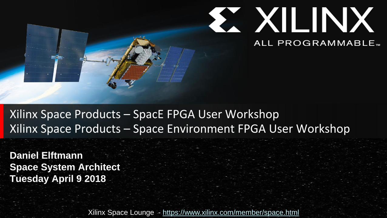
Xilinx Space Lounge - https://www.xilinx.com/member/space.html Xilinx Space Products – Space Environment FPGA User Workshop Daniel Elftmann Space System Architect Tuesday April 9 2018 Xilinx Space Products – SpacE FPGA User Workshop
Transcript of Xilinx Space Products SpacE FPGA User Workshop …...PCIe® Gen1/2/3 3 Interlaken 0 100G Ethernet 0...
Xilinx Space Lounge - https://www.xilinx.com/member/space.html
Xilinx Space Products – Space Environment FPGA User Workshop
Daniel Elftmann
Space System Architect
Tuesday April 9 2018
Xilinx Space Products – SpacE FPGA User Workshop
© Copyright 2018 Xilinx
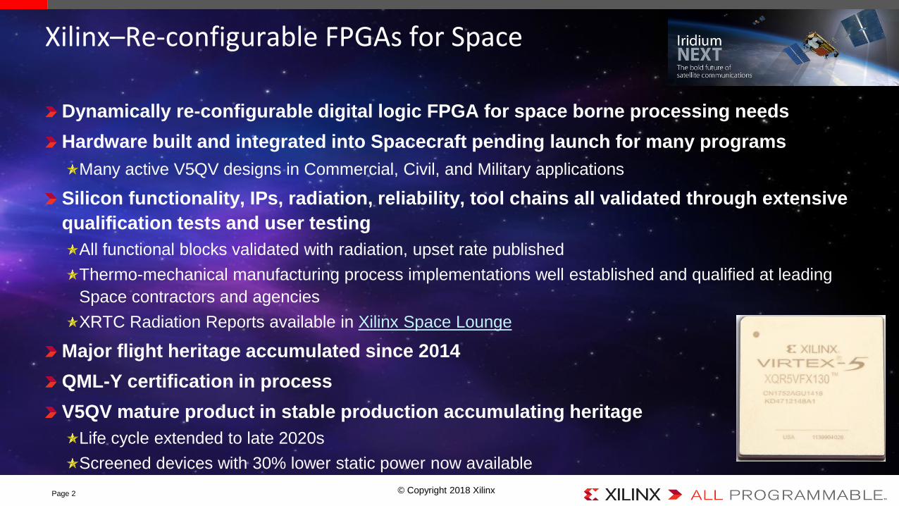
Dynamically re-configurable digital logic FPGA for space borne processing needs
Hardware built and integrated into Spacecraft pending launch for many programs
Many active V5QV designs in Commercial, Civil, and Military applications
Silicon functionality, IPs, radiation, reliability, tool chains all validated through extensive
qualification tests and user testing
All functional blocks validated with radiation, upset rate published
Thermo-mechanical manufacturing process implementations well established and qualified at leading
Space contractors and agencies
XRTC Radiation Reports available in Xilinx Space Lounge
Major flight heritage accumulated since 2014
QML-Y certification in process
V5QV mature product in stable production accumulating heritage
Life cycle extended to late 2020s
Screened devices with 30% lower static power now available
Page 2
Xilinx–Re-configurable FPGAs for Space
© Copyright 2018 Xilinx
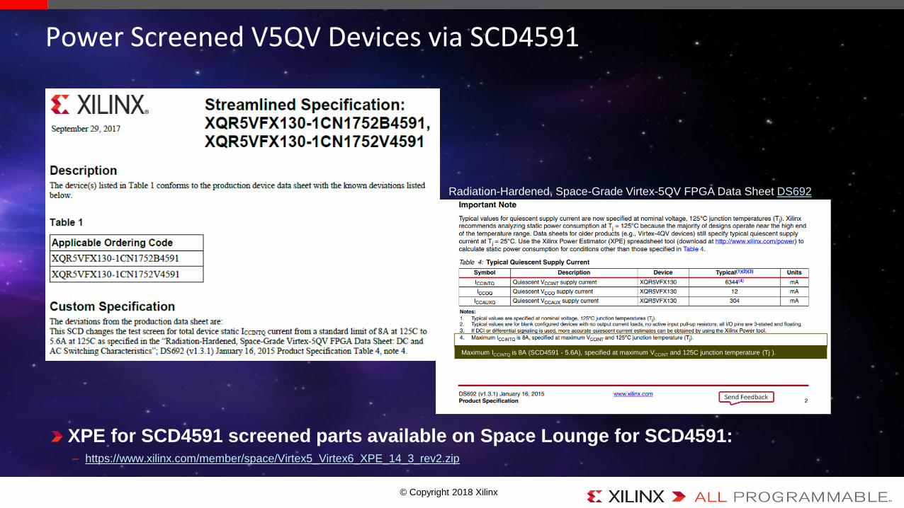
Power Screened V5QV Devices via SCD4591
Maximum ICCINTQ is 8A (SCD4591 - 5.6A), specified at maximum VCCINT and 125C junction temperature (Tj ).
Radiation-Hardened, Space-Grade Virtex-5QV FPGA Data Sheet DS692
XPE for SCD4591 screened parts available on Space Lounge for SCD4591:– https://www.xilinx.com/member/space/Virtex5_Virtex6_XPE_14_3_rev2.zip

© Copyright 2018 Xilinx
Xilinx chip capacitor vendor received conditional DLA slash sheet approval
– Conditional screening defined for increased voltage stress
– Vendor able to deliver chip capacitors meeting defined conditional screening in June, 2019
• Delays V5QV Class “Y” shipments to Q4’2019
• No impact to plans for XQRKU060 Class “Y”
Page 4
Xilinx Class “Y” Update

© Copyright 2018 XilinxPage 5
Missions with Virtex-5QV – More in Pipeline
DLR H2 Comm. Sat. (2020 Launch)
NovaSAR
(2018 Launch)
Iridium Next (66+6+9)See Xilinx Press Release
(First 50 Satellites deployed)
Glonass-K(2014)
Formosat-5(Launched August 24th 2017
SARah
(2019 Launch)
M-Cubed/COVE-2 Mission(2013)
Cosmo Skymed NextGen
(2018 Launch)“An FPGA based on-board processor platform for space application"”
Alexander Hofmann; Rainer Wansch; Robért Glein; Bernd Kollmannthaler
2012 NASA/ESA Conference on Adaptive Hardware and Systems (AHS)
“High performance, high volume reconfigurable processor architecture”
Paul Murray; Tres Randolph; Damon Van Buren; David Anderson; Ian Troxel
2012 IEEE Aerospace Conference
Multiple U.S. Classified Programs
“NovaSAR-S low cost spaceborne SAR payload design, development
and deployment of a new benchmark in spaceborne radar”
Martin Cohen; Andy Larkins; Pedro Lau Semedo; Geoff Burbidge
FORMOSAT-5 Development & Metrology Application
Ho-Pen Chang, Way-Jin Chen
A CubeSat design to validate the Virtex-5 FPGA for spaceborne
image processing
Dmitriy L. Bekker; Thomas A. Werne; Thor O. Wilson; Paula J.
Pingree; Kiril Dontchev; Michael Heywood; Rafael Ramos; Brad
Freyberg; Fernando Saca; Brian Gilchrist; Alec Gallimore; James
Cutler
© Copyright 2018 Xilinx
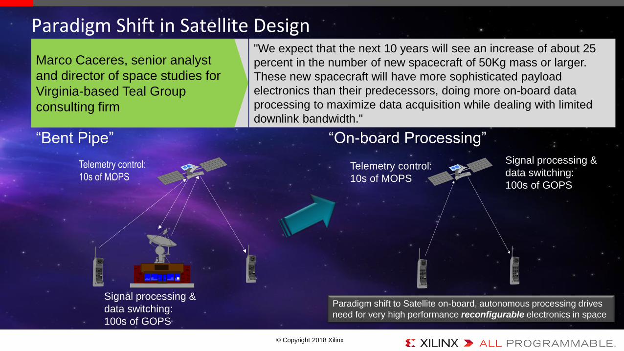
Paradigm Shift in Satellite Design"We expect that the next 10 years will see an increase of about 25
percent in the number of new spacecraft of 50Kg mass or larger.
These new spacecraft will have more sophisticated payload
electronics than their predecessors, doing more on-board data
processing to maximize data acquisition while dealing with limited
downlink bandwidth."
Marco Caceres, senior analyst
and director of space studies for
Virginia-based Teal Group
consulting firm
Paradigm shift to Satellite on-board, autonomous processing drives
need for very high performance reconfigurable electronics in space
Signal processing &
data switching:
100s of GOPS
Telemetry control:
10s of MOPS
“Bent Pipe” “On-board Processing”
Telemetry control:
10s of MOPS
Signal processing &
data switching:
100s of GOPS
© Copyright 2018 Xilinx
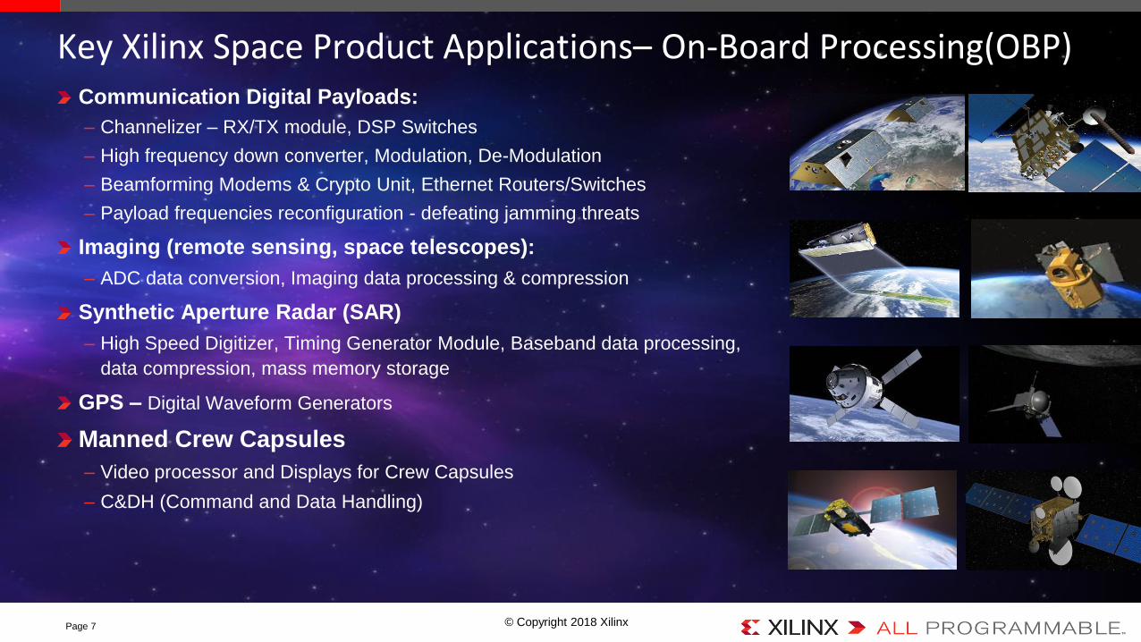
Communication Digital Payloads:
– Channelizer – RX/TX module, DSP Switches
– High frequency down converter, Modulation, De-Modulation
– Beamforming Modems & Crypto Unit, Ethernet Routers/Switches
– Payload frequencies reconfiguration - defeating jamming threats
Imaging (remote sensing, space telescopes):
– ADC data conversion, Imaging data processing & compression
Synthetic Aperture Radar (SAR)
– High Speed Digitizer, Timing Generator Module, Baseband data processing,
data compression, mass memory storage
GPS – Digital Waveform Generators
Manned Crew Capsules
– Video processor and Displays for Crew Capsules
– C&DH (Command and Data Handling)
Page 7
Key Xilinx Space Product Applications– On-Board Processing(OBP)

Xilinx Space Lounge - https://www.xilinx.com/member/space.html
XQR Kintex UltraScale KU060 for Space Applications
© Copyright 2018 XilinxPage 9
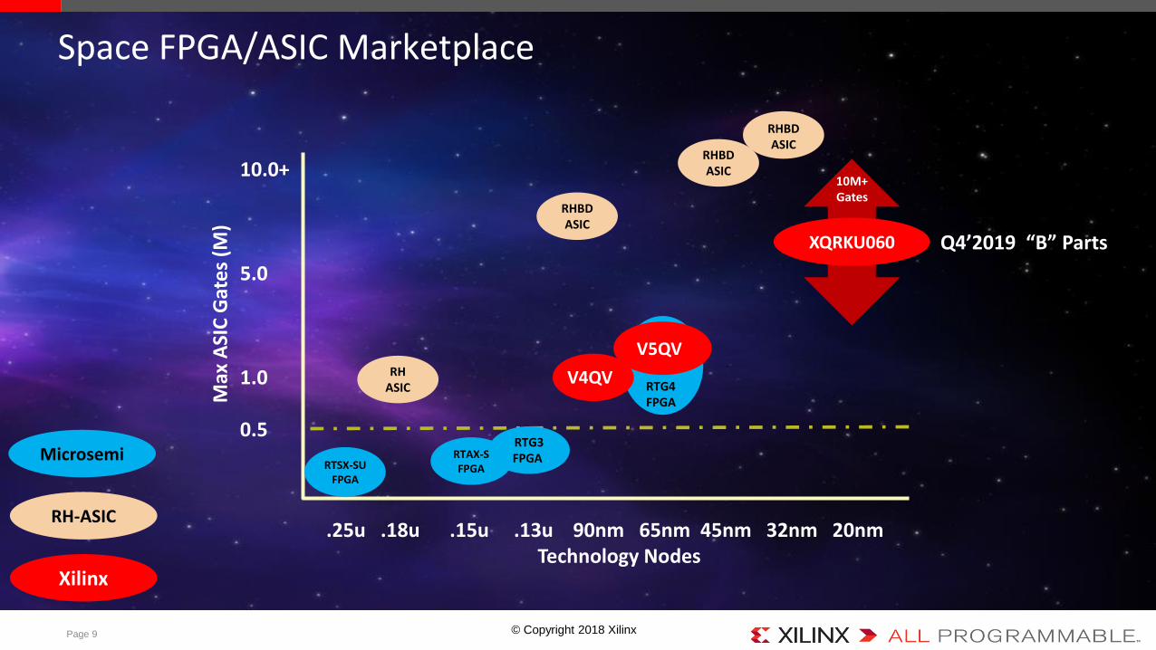
Space FPGA/ASIC Marketplace
RTG4FPGA
.25u .18u .15u .13u 90nm 65nm 45nm 32nm 20nmTechnology Nodes
10.0+
5.0
1.0
0.5
Max
ASI
C G
ate
s (M
)
RTSX-SU FPGA
RHASIC
RHBDASIC
RHBDASIC
V5QV
RTG3FPGA
V4QV
RHBDASIC
RH-ASIC
Microsemi
Xilinx
XQRKU060
10M+Gates
RTAX-S FPGA
Q4’2019 “B” Parts
© Copyright 2018 Xilinx
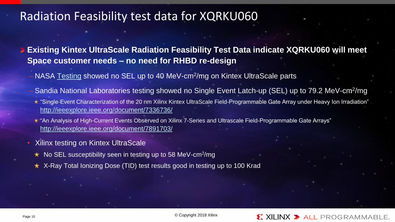
Existing Kintex UltraScale Radiation Feasibility Test Data indicate XQRKU060 will meet
Space customer needs – no need for RHBD re-design
– NASA Testing showed no SEL up to 40 MeV-cm2/mg on Kintex UltraScale parts
– Sandia National Laboratories testing showed no Single Event Latch-up (SEL) up to 79.2 MeV-cm2/mg
“Single-Event Characterization of the 20 nm Xilinx Kintex UltraScale Field-Programmable Gate Array under Heavy Ion Irradiation”
http://ieeexplore.ieee.org/document/7336736/
“An Analysis of High-Current Events Observed on Xilinx 7-Series and Ultrascale Field-Programmable Gate Arrays”
http://ieeexplore.ieee.org/document/7891703/
• Xilinx testing on Kintex UltraScale
No SEL susceptibility seen in testing up to 58 MeV-cm2/mg
X-Ray Total Ionizing Dose (TID) test results good in testing up to 100 Krad
Page 10
Radiation Feasibility test data for XQRKU060
© Copyright 2018 Xilinx
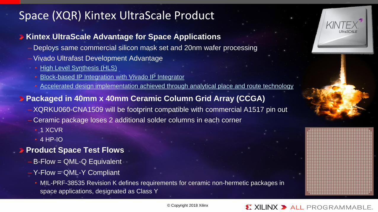
Kintex UltraScale Advantage for Space Applications
– Deploys same commercial silicon mask set and 20nm wafer processing
– Vivado Ultrafast Development Advantage
• High Level Synthesis (HLS)
• Block-based IP Integration with Vivado IP Integrator
• Accelerated design implementation achieved through analytical place and route technology
Packaged in 40mm x 40mm Ceramic Column Grid Array (CCGA)
– XQRKU060-CNA1509 will be footprint compatible with commercial A1517 pin out
– Ceramic package loses 2 additional solder columns in each corner
• 1 XCVR
• 4 HP-IO
Product Space Test Flows
– B-Flow = QML-Q Equivalent
– Y-Flow = QML-Y Compliant
• MIL-PRF-38535 Revision K defines requirements for ceramic non-hermetic packages in
space applications, designated as Class Y
Space (XQR) Kintex UltraScale Product

© Copyright 2018 XilinxPage 12
XC Commercial Package Transceiver Locations
The ceramic package (CNA1509) pinout for Space
Product compatible with A1517 configuration
– Difference being additional two pins in each corner removed from Ceramic
Column Grid Array package for shock, vibe, and handling considerations
– Ceramic package loses 2 additional solder columns in each corner
• 1 XCVR
• 4 HP/IO
– In the case of the A1517 => A1509 I/O pins to avoid or not use:
Bank/Quad Pin Note
Quad 224 AV1 MGTHRXN1, thus also AV2 (MGTHRXP1) – Relocated to T1/T2
Bank 25 AV39 IO_L8N, thus AV38 (IO_L8P) unusable as differential pair
Bank 25 AV38 Single-ended IO
Bank 46 A38 (IO_L17N), thus also A37(IO_L17P) unusable as differential pair
Bank 46 B39 (IO_L16N), thus also C38(IO_L16P) unusable as differential pairUG575 UltraScale and UltraScale+ FPGAs Packaging and Pinouts
CNA1509 (XCKU060)
CNA1509 Package – XCKU060 I/O Bank Diagram
© Copyright 2018 Xilinx
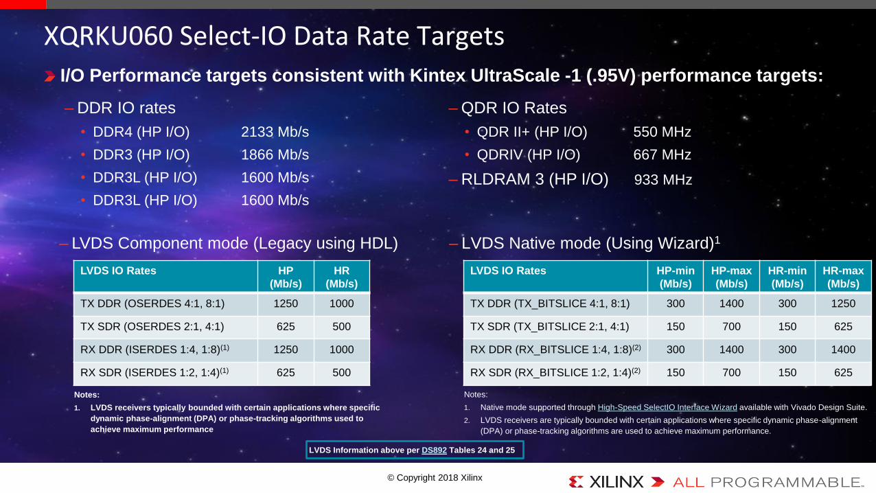
I/O Performance targets consistent with Kintex UltraScale -1 (.95V) performance targets:
XQRKU060 Select-IO Data Rate Targets
– LVDS Native mode (Using Wizard)1
LVDS IO Rates HP-min
(Mb/s)
HP-max
(Mb/s)
HR-min
(Mb/s)
HR-max
(Mb/s)
TX DDR (TX_BITSLICE 4:1, 8:1) 300 1400 300 1250
TX SDR (TX_BITSLICE 2:1, 4:1) 150 700 150 625
RX DDR (RX_BITSLICE 1:4, 1:8)(2) 300 1400 300 1400
RX SDR (RX_BITSLICE 1:2, 1:4)(2) 150 700 150 625
Notes:
1. LVDS receivers typically bounded with certain applications where specific
dynamic phase-alignment (DPA) or phase-tracking algorithms used to
achieve maximum performance
Notes:
1. Native mode supported through High-Speed SelectIO Interface Wizard available with Vivado Design Suite.
2. LVDS receivers are typically bounded with certain applications where specific dynamic phase-alignment
(DPA) or phase-tracking algorithms are used to achieve maximum performance.
– LVDS Component mode (Legacy using HDL)
LVDS IO Rates HP
(Mb/s)
HR
(Mb/s)
TX DDR (OSERDES 4:1, 8:1) 1250 1000
TX SDR (OSERDES 2:1, 4:1) 625 500
RX DDR (ISERDES 1:4, 1:8)(1) 1250 1000
RX SDR (ISERDES 1:2, 1:4)(1) 625 500
– DDR IO rates
• DDR4 (HP I/O) 2133 Mb/s
• DDR3 (HP I/O) 1866 Mb/s
• DDR3L (HP I/O) 1600 Mb/s
• DDR3L (HP I/O) 1600 Mb/s
– QDR IO Rates
• QDR II+ (HP I/O) 550 MHz
• QDRIV (HP I/O) 667 MHz
– RLDRAM 3 (HP I/O) 933 MHz
LVDS Information above per DS892 Tables 24 and 25
© Copyright 2018 Xilinx
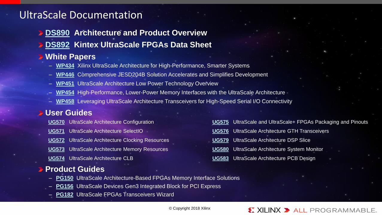
UltraScale Documentation
DS890 Architecture and Product Overview
DS892 Kintex UltraScale FPGAs Data Sheet
White Papers – WP434 Xilinx UltraScale Architecture for High-Performance, Smarter Systems
– WP446 Comprehensive JESD204B Solution Accelerates and Simplifies Development
– WP451 UltraScale Architecture Low Power Technology Overview
– WP454 High-Performance, Lower-Power Memory Interfaces with the UltraScale Architecture
– WP458 Leveraging UltraScale Architecture Transceivers for High-Speed Serial I/O Connectivity
User Guides
Product Guides– PG150 UltraScale Architecture-Based FPGAs Memory Interface Solutions
– PG156 UltraScale Devices Gen3 Integrated Block for PCI Express
– PG182 UltraScale FPGAs Transceivers Wizard
UG570 UltraScale Architecture Configuration UG575 UltraScale and UltraScale+ FPGAs Packaging and Pinouts
UG571 UltraScale Architecture SelectIO UG576 UltraScale Architecture GTH Transceivers
UG572 UltraScale Architecture Clocking Resources UG579 UltraScale Architecture DSP Slice
UG573 UltraScale Architecture Memory Resources UG580 UltraScale Architecture System Monitor
UG574 UltraScale Architecture CLB UG583 UltraScale Architecture PCB Design
© Copyright 2018 XilinxPage 15
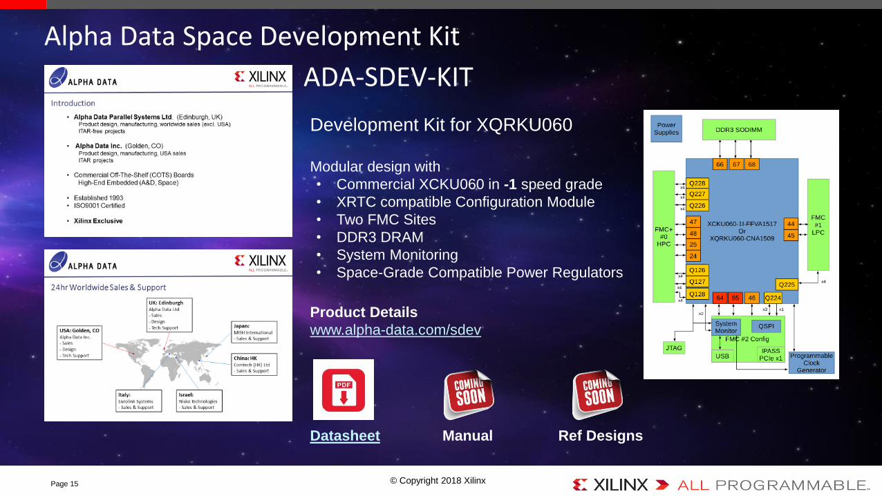
Alpha Data Space Development Kit
ADA-SDEV-KIT
Development Kit for XQRKU060
Modular design with
• Commercial XCKU060 in -1 speed grade
• XRTC compatible Configuration Module
• Two FMC Sites
• DDR3 DRAM
• System Monitoring
• Space-Grade Compatible Power Regulators
Product Details
www.alpha-data.com/sdev
Datasheet Manual Ref Designs

© Copyright 2018 XilinxPage 16
For retro-perspective: V4QV & V5QV Resource Table
XQR4V(Radiation Tolerant, 1.2V)
XQR5V (RH-BD, 1.0V)
SX55 FX60 FX140 LX200 FX130
Logic Cells 55,296 56,880 142,128 200,448 131,072
CLB Flip-Flops 49,152 50,560 126,336 178,176 81,920
Distributed RAM (Kbits) 384 395 987 1,392 1,580
Total Block RAM (Kbits) 5,760 4,176 9,936 6,048 10,728
Digital Clock Manager (DCM) 8 12 20 12 12
Phase Lock Loop (PLL) --- --- --- --- 6
DSP Slices 512 128 192 96 320
350 MHz PPC405 Cores --- 2 2 --- ---
10/100/1000 EMACs --- 4 4 --- 6
Multi-Gigabit Transceivers (MGT) --- --- --- --- 18
TID (krad) 300 300 300 300 1,000
SEL Immunity (LETs) >125 >125 >125 >125 >125
Package
Size (mm) 35 x 35 mm 40 x 40 mm 45 x 45 mm
Pin Counts 1140 1144 1509 1752
Max. IO Count 640 576 768 960 840
Daisy Chain Yes Yes Yes Yes
© Copyright 2018 XilinxPage 17
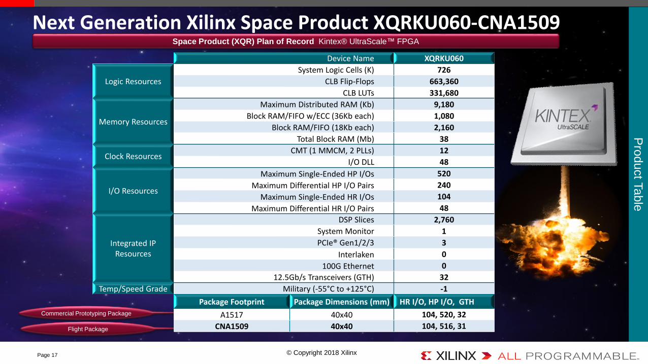
Next Generation Xilinx Space Product XQRKU060-CNA1509P
roduct T
able
Space Product (XQR) Plan of Record Kintex® UltraScale™ FPGA
Flight Package
Commercial Prototyping Package
Device Name XQRKU060
Logic Resources
System Logic Cells (K) 726
CLB Flip-Flops 663,360
CLB LUTs 331,680
Memory Resources
Maximum Distributed RAM (Kb) 9,180
Block RAM/FIFO w/ECC (36Kb each) 1,080
Block RAM/FIFO (18Kb each) 2,160
Total Block RAM (Mb) 38
Clock ResourcesCMT (1 MMCM, 2 PLLs) 12
I/O DLL 48
I/O Resources
Maximum Single-Ended HP I/Os 520
Maximum Differential HP I/O Pairs 240
Maximum Single-Ended HR I/Os 104
Maximum Differential HR I/O Pairs 48
Integrated IP Resources
DSP Slices 2,760
System Monitor 1
PCIe® Gen1/2/3 3
Interlaken 0
100G Ethernet 0
12.5Gb/s Transceivers (GTH) 32
Temp/Speed Grade Military (-55°C to +125°C) -1
Package Footprint Package Dimensions (mm) HR I/O, HP I/O, GTH
A1517 40x40 104, 520, 32
CNA1509 40x40 104, 516, 31

© Copyright 2018 Xilinx
Early programs proceeding directly to development
– Pin compatible commercial XCKU060/A1517 device available now!
– Target XCKU060-1FFVA1517I (-1 Speed Grade) in Vivado software
– Alpha Data Space Development Kit (ADA-SDEV-KIT)
Flight Part Schedule
– April 2018 – Package Design Release
– October 2018 – All piece parts available to begin assembly and test of qualification units
– December 2018 – Pre-qualification Ready (Operations Space Test Flow hardware and procedures)
– June 2019 – Complete pre-qualification validation with full qualification unit quantities
– December 2019 – “B” Availability XQRKU060-CNA1509B
– December 2020 – “Y” Availability XQRKU060-CNA1509Y
Page 18
Preliminary XQRKU060-CNA1509 Schedule
DLR H2 Communication Satellite
Xilinx Space Lounge - https://www.xilinx.com/member/space.html
Kintex UltraScale (KU060) Architecture for Space Applications

© Copyright 2018 XilinxPage 20
Vivado Design Suite Enables the UltraScale Advantage
Tim
ing
Co
st
f(x
)
Placement Solution x
(found by random moves and seeds)
initial random seed
best solution found
not routable
Local moves
optimal solution
(not found)
Next Generation Implementation
© Copyright 2018 Xilinx
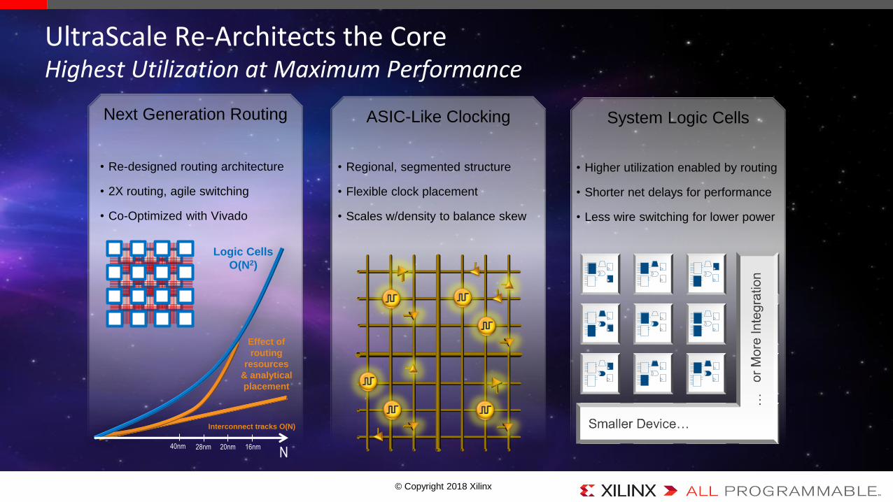
UltraScale Re-Architects the CoreHighest Utilization at Maximum Performance
Next Generation Routing
• Re-designed routing architecture
• 2X routing, agile switching
• Co-Optimized with Vivado
ASIC-Like Clocking
• Regional, segmented structure
• Flexible clock placement
• Scales w/density to balance skew
System Logic Cells
• Higher utilization enabled by routing
• Shorter net delays for performance
• Less wire switching for lower power
Effect of
routing
resources
& analytical
placement
Logic Cells
O(N2)
Interconnect tracks O(N)
40nm 28nmN
20nm 16nm

© Copyright 2018 Xilinx
DSP48E2
Slice
DSP48E2
Slice
5 high speed
Interconnects
DSP48 Tile
Page 22
Enhanced DSP Sub-Systems for Performance and Efficiency
Feature Benefit
27x18 multiplier in a DSP slice;
35x28 support in a DSP tile (2 slices)
• Optimal performance per block
• Implement double-precision floating point in two-thirds the fabric
Pre-adder squaring• More efficient motion estimation in video applications
• Perform “sum-of-square-difference” calculations in 50% fewer resources
Extra accumulator feedback path Implement complex multiply-accumulate in half the resources
Wide XOR Implement EFEC, CRC, ECC functionality
White box modeling Full visibility with accurate simulation and debug
© Copyright 2018 XilinxPage 23
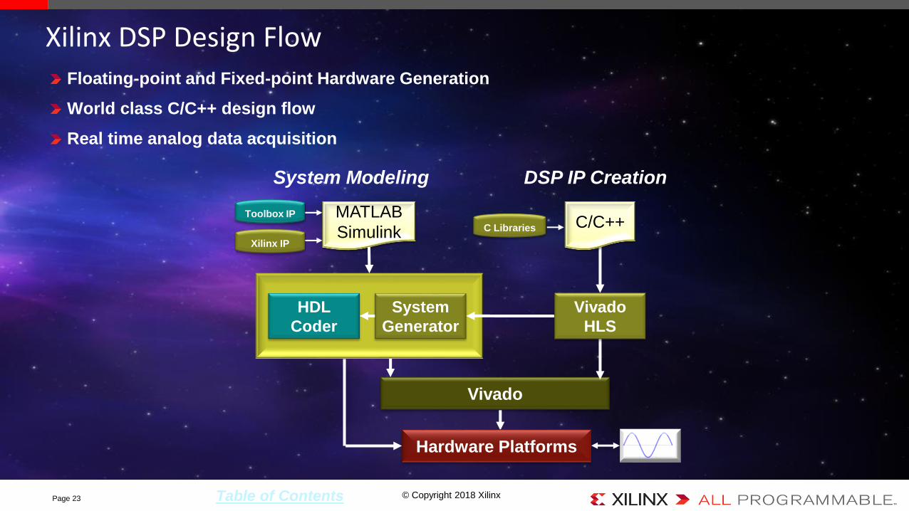
Xilinx DSP Design FlowFloating-point and Fixed-point Hardware Generation
World class C/C++ design flow
Real time analog data acquisition
HDL
Coder
System
Generator
Vivado
Toolbox IP
Xilinx IP
MATLAB
SimulinkC/C++C Libraries
System Modeling DSP IP Creation
Table of Contents
Vivado
HLS
Hardware Platforms
© Copyright 2018 XilinxPage 24
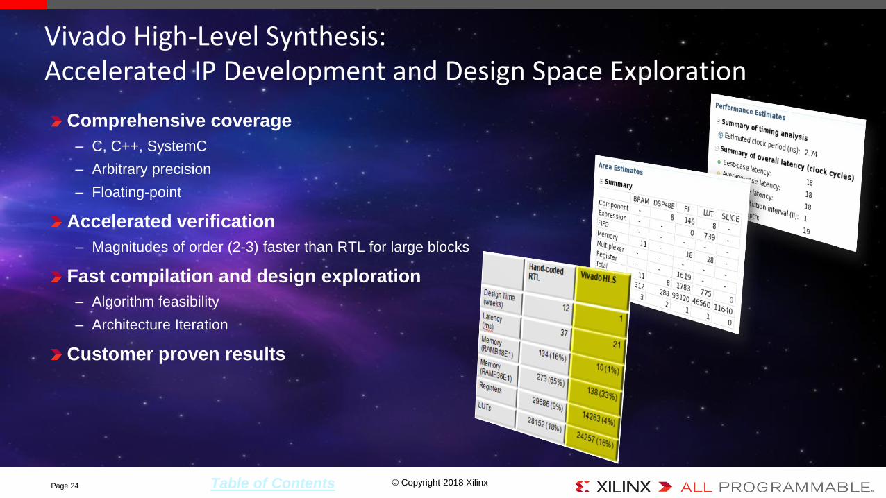
Vivado High-Level Synthesis: Accelerated IP Development and Design Space Exploration
Comprehensive coverage
– C, C++, SystemC
– Arbitrary precision
– Floating-point
Accelerated verification
– Magnitudes of order (2-3) faster than RTL for large blocks
Fast compilation and design exploration
– Algorithm feasibility
– Architecture Iteration
Customer proven results
Table of Contents
© Copyright 2018 XilinxPage 25
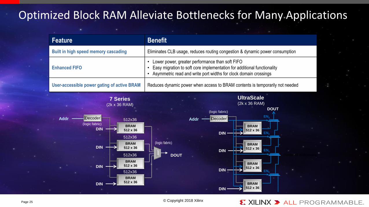
Optimized Block RAM Alleviate Bottlenecks for Many Applications
Feature Benefit
Built in high speed memory cascading Eliminates CLB usage, reduces routing congestion & dynamic power consumption
Enhanced FIFO
• Lower power, greater performance than soft FIFO
• Easy migration to soft core implementation for additional functionality
• Asymmetric read and write port widths for clock domain crossings
User-accessible power gating of active BRAM Reduces dynamic power when access to BRAM contents is temporarily not needed
7 Series(2k x 36 RAM)
BRAM
512 x 36
512x36
BRAM
512 x 36
512x36
BRAM
512 x 36
512x36
BRAM
512 x 36
512x36
(logic fabric)
Addr Decoder
(logic fabric)
UltraScale(2k x 36 RAM)
BRAM
512 x 36
BRAM
512 x 36
BRAM
512 x 36
BRAM
512 x 36DIN
DIN
DIN
DIN
DOUT
(hardened multiplexers)
DIN
DIN
DIN
DIN
Addr
(logic fabric)
Decoder
DOUT
EN0
EN1
EN2
EN3

© Copyright 2018 Xilinx
Kintex-7 vs. KintexUltraScale
Virtex-7 vs. VirtexUltraScale
800
2,784
1,536
5,616
2x Aggregate Bandwidth (Gb/s)
Kintex-7
(GTX)
Kintex UltraScale
(GTH)
Page 26
Delivering Massive I/O Serial Bandwidth
10G Backplanes
Half the Power
7 Series
UltraScale
~40% Lower
16+ Gb/s
30.5 Gb/s
Virtex
UltraScale
Kintex
UltraScale
GTH GTH
GTY
Feature Benefit
GTH
• 12.5Gb/s performance in -1 Speed and Military Temperature Grade
• Enabled Standards:
• PCIe Gen3
• JESD204B
• Xilinx Aurora
• Serial RapidIO (SRIO) – Space VPX (VITA 78) / Next Generation Space Interconnect Standard (NGSIS)
• NGSIS IP Core from Alliance Program Partner, Praesum Communications, developed on UltraScale Architecture
Major power reduction ~40% lower power over 7-Series for 10G backplanes
Continuous auto-adaptive equalization Continuously optimizes link margin over PVT in increasingly challenging channel conditions
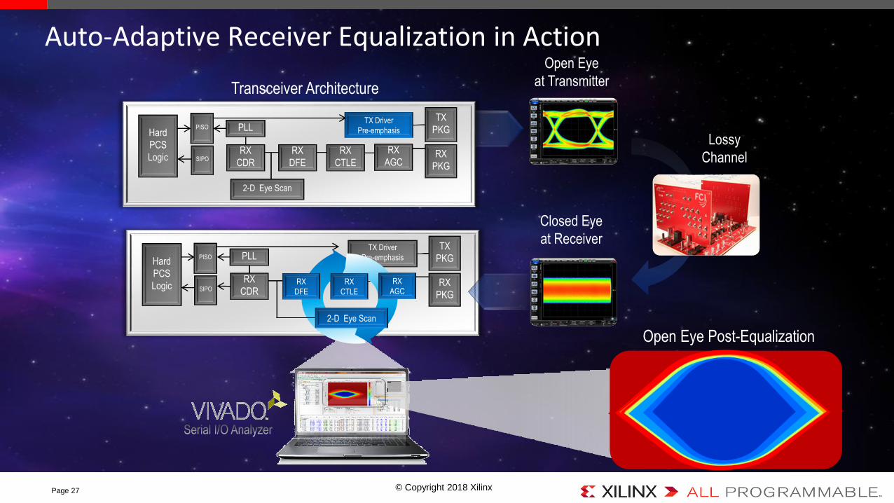
© Copyright 2018 Xilinx
Hard
PCS
Logic
PLL
RX
CDRRX
DFE
TX Driver
Pre-emphasis
TX
PKG
RX
PKG
RX
CTLE
RX
AGC
Page 27
Auto-Adaptive Receiver Equalization in Action
RX
DFE
RX
CTLE
RX
AGC
Open Eye
at Transmitter
Closed Eye
at Receiver
Hard
PCS
Logic SIPO
PLL
RX
CDRRX
DFE
TX Driver
Pre-emphasis
TX
PKG
RX
PKG
RX
CTLE
RX
AGC
PISO
2-D Eye Scan
RX
DFE
RX
CTLE
RX
AGC
Transceiver Architecture
SIPO
PISO
Open Eye Post-Equalization
2-D Eye Scan
Lossy
Channel
© Copyright 2018 Xilinx
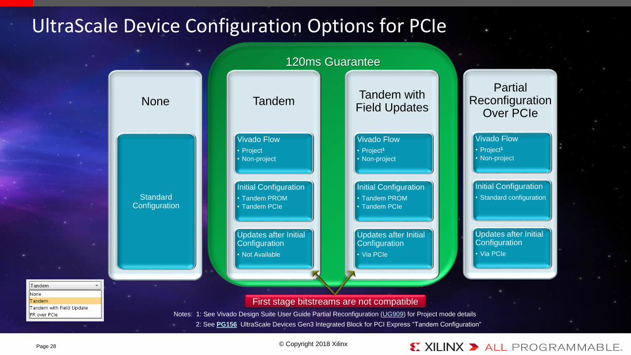
120ms Guarantee
Page 28
UltraScale Device Configuration Options for PCIe
None
Standard Configuration
Tandem
Vivado Flow
• Project
• Non-project
Initial Configuration
• Tandem PROM
• Tandem PCIe
Updates after Initial Configuration
• Not Available
Tandem with Field Updates
Vivado Flow
• Project1
• Non-project
Initial Configuration
• Tandem PROM
• Tandem PCIe
Updates after Initial Configuration
• Via PCIe
PartialReconfiguration
Over PCIe
Vivado Flow
• Project1
• Non-project
Initial Configuration
• Standard configuration
Updates after Initial Configuration
• Via PCIe
First stage bitstreams are not compatible
Notes: 1: See Vivado Design Suite User Guide Partial Reconfiguration (UG909) for Project mode details
2: See PG156 UltraScale Devices Gen3 Integrated Block for PCI Express “Tandem Configuration“

© Copyright 2018 XilinxPage 29
MicroBlaze Triple Modular Redundancy (TMR) SubsystemMicro-controller systems
Derived from MicroBlaze TMR designed for Zynq Ultrascale+ MPSoC PMU & CSU
– Add redundancy to detect failures and recover from faults without disrupting application
– Use Vivado IP Integrator to automate creation of a TMR system using handful of new IPs
– Partitioning into IP building blocks with automated triplication in Vivado
MicroBlaze TMR Fundamentals
– Triplication (TMR) for Fail Tolerant–Fail Safe (FT-FS)
• First failure; continue nominal operation without degradation
• Second failure; detect failure and halt operation
– Duplication (Lockstep) for Fail-Safe (FS)
• First failure; detect failure and halt operation
Triplicate MicroBlaze sub-system
– Voting at boundary
– Recovery of failing CPU under SW control (seen by application as servicing interrupt)
MicroBlaze Triple Modular Redundancy (TMR) Subsystem v1.0 Product Guide
– https://www.xilinx.com/support/documentation/ip_documentation/tmr/v1_0/pg268-tmr.pdf
© Copyright 2018 Xilinx
It is the stated policy of Xilinx to only provide radiation performance data, guidance or support for the use of Xilinx products in Space
Radiation Environment applications for products designated as Xilinx Space (XQR) products. As such, Xilinx will not provide this
type of data, guidance or support for non-XQR products. The Space Radiation Environment is a branch of astronautics, aerospace
engineering and space physics that seeks to understand and address conditions existing in space that affect the design and
operation of spacecraft, launch vehicles and associated electronic systems. Only Xilinx Space (XQR) products are specified and
endorsed for use in the space environment. The Xilinx standard terms and conditions1 state that the Xilinx Limited Warranty does
not apply to and excludes to the maximum extent permitted by applicable law “Products used in an application or environment that is
not within the Specifications”. Customers choosing to use Xilinx products in space environments that are not specified for use in
space do so entirely at their own risk.
• Xilinx continues to support Xilinx Radiation Test Consortium (XRTC) weekly conference calls and annual meeting
• Xilinx does post XRTC proceedings from annual meeting in the Xilinx Space Lounge under agreement with XRTC
• Do note that the XRTC is a distinct and separate organization from Xilinx
• Current chairperson for the XRTC is Gary Swift, who can be contacted via the information below:
Swift Engineering and Radiation Services, LLC
408-628-4803 (landline) or 408-679-3785 (cell)
email: [email protected]
http://xrtc.groups.et.byu.net/wiki/doku.php
Page 30
Space Policy for non-XQR Parts
1: Except only where otherwise agreed in writing signed by an officer of Xilinx, all offers and sales by Xilinx of goods and services are governed exclusively by Xilinx’ Terms of Sale, which can be found at: http://www.Xilinx.com/legal.htm#tos
© Copyright 2018 Xilinx
Lowest risk choices are V4QV and V5QV space products, then schedule permitting
XQRKU060
– Space products available in Ceramic Column Grid Array package with Space Test flows (“B”, “V”, “Y”)
With Space Policy clearly in mind, for select programs with approved business case
discussions for non-XQR product following conditions apply
– Customer must be capable and willing to use a Defense Grade (XQ) product
• Defense Grade (XQ) value attributes appeal to their needs, such as:
– Full range extended temperature testing at Military temperature extremes
– Full compliance with MIL-PRF-38535 Pb content standards
– Ruggedized packaging- MIL-STD-883 group D Qualification tested for Defense Grade products prior to product release
– Single Lot Date Code (SLDC) orders possible for customer to perform their own additional qualification
• Orders must be NCNR- Customer takes on the Lot Jeopardy, not Xilinx
• SLDC option incurs increased pricing (contact factory)
– Total Ionizing Dose (TID) testing requires significant NRE for initial setup and characterization
– High Temperature Operating Life testing requires an even larger NRE and is strongly discouraged
– No Single Event Effect performance test requests:
• Customer must either work with the XRTC or make determination from their own independent testing results
Page 31
Space 2.0 Approach

© Copyright 2018 XilinxPage 32