World s First 2D Multi-Touch Pad with 3D Gesture...
34
World’s First 2D Multi-Touch Pad with 3D Gesture Recognition Winter 2012 SENSORS ROBUST COMPACT IoT APPS CONTROL Nov/Dec 2014
Transcript of World s First 2D Multi-Touch Pad with 3D Gesture...
World’s First2D Multi-Touch Pad with3D Gesture Recognition
Winter 2012
SENSORSROBUST COMPACT IoT APPS CONTROL
Nov/Dec 2014

The Microchip name and logo, the Microchip logo, dsPIC, FlashFlex, KEELOQ, KEELOQ logo, MPLAB, mTouch, PIC, PICmicro, PICSTART, PIC32 logo, rfPIC, SST, SST Logo, SuperFlash and UNI/O are registered trademarks of Microchip Technology Incorporated in the U.S.A. and other countries. FilterLab, Hampshire, HI-TECH C, Linear Active Thermistor, MTP, SEEVAL and The Embedded Control Solutions Company are registered trademarks of Microchip Technology Incorporated in the U.S.A. Silicon Storage Technology is a registered trademark of Microchip Technology Inc. in other countries.Analog-for-the-Digital Age, Application Maestro, BodyCom, chipKIT, chipKIT logo, CodeGuard, dsPICDEM, dsPICDEM.net, dsPICworks, dsSPEAK, ECAN, ECONOMONITOR, FanSense, HI-TIDE, In Circuit Serial Programming, ICSP, Mindi, MiWi, MPASM, MPF, MPLAB Certified logo, MPLIB, MPLINK, Omniscient Code Generation, PICC, PICC-18, PICDEM, PICDEM.net, PICkit, PICtail, REAL ICE, rfLAB, Select Mode, SQI, Serial Quad I/O, Total Endurance, TSHARC, UniWinDriver, WiperLock, ZENA and Z-Scale are trademarks of Microchip Technology Incorporated in the U.S.A. and other countries.SQTP is a service mark of Microchip Technology Incorporated in the U.S.A. GestIC and ULPP are registered trademarks of Microchip Technology Germany II GmbH & Co. & KG, a subsidiary of Microchip Technology Inc., in other countries. All other trademarks mentioned herein are property of their respective companies. © 2014, Microchip Technology Incorporated, All Rights Reserved.
ContentsDESIGN ARTICLES18 Measuring Heart Rate and
Blood Oxygen Levels for Portable and Wearable Devices
23 Buck-Based LED Drivers Using the HV9910B
27 Connected Things Are the Future of Mobile
29 A Complete Solution for Mesh Networks
31 Printed Multi-Touch Sensor Solutions for Modern Designs
32 Accelerating Low-Level Code Implementation in PIC32 MCU Applications
FEATURES15 Product Spotlight16 Gifts Just For You33 Connect With Us at 2015
International CES
SHOWCASE 4 A Touch Above
3DTouchPad is world’s first 2D multi-touch pad with 3D gesture recognition
NEW PRODUCTS 6 Take Control
8-bit microcontroller family offers closed-loop digital control and safety monitoring
8 When the Going Gets Tough5V dsPIC33 “EV” family offers enhanced noise immunity and robustness for harsh environments
9 Smart MixLatest 32-bit microcontrollers enable a wide range of applications at lower prices
11 Very PreciseNew high-speed devices feature industry’s lowest-power 16-bit, 200 Msps stand-alone ADCs
12 Swapping RolesUSB 2.0 four-port controller hub connects smartphones to automotive infotainment systems
14 Power UpGet simple analog PWM control and configurable MCU in compact circuit solution
2
Nov/Dec 2014
2

Don’t Miss the Next Issue of MicroSolutions
Published six times a year, MicroSolutions is a valuable resource for product and technology news about Microchip’s innovative solutions. Subscribe today to receive email notifications when each new issue of MicroSolutions is ready. If you prefer, you can be notified via our RSS feed. Use the links below:
To get the latest news about Microchip and its products via social media, be sure to Like Us on Facebook and Follow Us on Twitter:
EDITOR’S NOTE
Find us on these social channels:
Microchip Technology Inc. 2355 W. Chandler Blvd. | Chandler, AZ 85224 | www.microchip.com
3
We'd Like Your Help
Did you know that the size and scope of the Microchip website has exploded within the past several years? Our product offerings have been steadily expanding, reaching into a growing variety of innovative and leading-edge
applications. At the same time, we've absorbed extensive product information from a series of significant company acquisitions that occurred during this same time frame. Needless to say, as our business continues to expand, the additional activity keeps our web development team very busy.
Our website is the "go to" resource for many thousands of visitors monthly who need help selecting a product, developing an application, or learning about new technol-ogies. They can visit our Design Centers, download software and other resources, submit requests for technical support or get information on our training programs. Recognizing that requirements and technology are constantly evolving, our goal is to continuously enhance the features on our website to offer the best experience possible to all our users. That's where you come in.
We would very much appreciate it if you would take just a couple of minutes to assist us as we plan for the future of the Microchip website. We have developed a simple online survey which will help us learn how you currently use our website, how well it is working for you, and how we can make updates so that it continues to meet your needs going forward. While the majority of the questions can be easily answered using checkboxes and buttons, you will also have the opportunity to provide additional com-ments if you have any suggestions for us. Click the text below to access the survey: Microchip Website Survey
As always, we would be happy to get your feedback on MicroSolutions. Feel free to email us at [email protected].

It provides an intuitive and easy way to control the
flow of content.
SHOWCASE
4
Have you ever used free-space gestures to control your PC? Our new 3DTouchPad (DM160225) is an
innovative PC accessory which works out of the box to provide you with a range of options for using touch and gestures to interact with your PC. It is also the first development platform for the PC/peripheral market that features 2D multi-touch and 3D gestures, enabling you to easily design advanced human-interface capabilities into your latest products.
The 3DTouchPad blends our highly responsive projected capacitive (PCAP) sensor solutions with our patented GestIC® technology for
A Touch Above3DTouchPad is World’s First 2D Multi-Touch Pad with 3D Gesture Recognition
Rich and Well-Documented Development Platform Enables Advanced Human-Interface Capabilities for Leading-Edge Applications
3D gesture recognition at a range of up to 10 centimeters. It offers all the features you would expect from a touchpad, including sup-port for precision, multi-finger tracking as well as multi-finger surface gestures like swipes
and scrolling. With the addition of support for 3D hand gestures, the 3DTouchPad also provides an intuitive and easy way to control the flow of content. For example,
you can browse through pictures on your PC using just a wave of your hand or control the volume of your PC’s speakers by circling your hand using an air wheel gesture.
As a PC peripheral, the 3DTouchPad supports Windows® 7/8, OS X® and other major operating
As a PC peripheral, the 3DTouchPad provides out-of-the-box support for all major operating systems.
(continued on page 5)
Figure 1 - 3DTouchPad System Diagram

used to perform a variety of input commands. A free Graphical User Interface (GUI) allows you to access all the data that is generated by the 3DTouchPad.
If you’re ready to get started, it's easy to add 2D and 3D human-interface capabilities to your design. The 3DTouchPad costs $99.00 and can be ordered from microchipDIRECT. Visit the 3DTouchPad page for additional information including documentation and downloads for the latest software and firm-ware releases. Be sure to also watch our 3DTouchPad video to learn more.
The possibilities for this advanced blend of human-to-machine interface technol-ogies reach beyond the PC market and computer touchpads to include hands-free sanitary products, home automation, game controllers, remote controls, wearable devices, automotive and other applications. Using the available features, demonstrations and sample code for the 3DTouchPad, you can unleash your creativity to develop a variety of engaging applications such as:
• Auto wake-on-proximity or gesture• Media center control
• Air wheel for volume control• Flicks for previous/next track
• Games based on 3D positioning• Virtual joystick
• Content-aware gesture mapping
In addition to its out-of-the-box features, the 3DTouchPad comes with a rich and well-documented Software Development Kit (SDK) and Application Programming Interface (API). The SDK gives you access to the Colibri Gesture Suite, our easy-to-use library of high-resolution x/y/z hand position tracking, flick, circle, and touch gestures
systems, with no driver installation required. Simply connect the 3DTouchPad to your PC using the provided USB cable and it will be automatically detected as a ready-to-use Human Interface Device (HID). It is fully com-patible with Windows 8 requirements, allow-ing you to use the two-finger scrolling and edge swipes that are part of the Windows 8 user experience.
SHOWCASE
5
2D Touchpad
Multi Touch Pinch/Zoom Scrolling
JoystickPC Wake-Up
Content Browsing
Volume/Brightness
3D Free Space Gestures Mapped to Windows® Events

This broad mix enables a wide
variety of functions.
NEW PRODUCT
6
Developed to take our 8-bit PIC® microcontroller (MCU) performance to a new level, Core Independent
Peripherals (CIP) can simplify the implementa-tion of complex control systems and give you the flexibility you need to create innovative designs. These peripherals are designed to reduce system complexity by eliminating the need for additional code and external com-ponents. Hardware-based peripherals offload timing-critical and core-intensive functions from the CPU, allowing it to focus on other critical tasks within the system.
As the latest additions to our 8-bit product portfolio, the peripheral-rich PIC16(L)F161X family of devices offers an expanded selection of Core Independent Peripherals to give you even more control over your design. This broad mix enables a wide variety of functions includ-ing motor control and safety monitoring so that you can create functions for closed-loop control with little-to-no interaction with the core. These capabilities allow you to create customizable functions specific to your application while minimizing your code development.
These new devices feature a Math Accelerator (Math ACC) with Proportional Integral Derivative
Take ControlNew 8-bit Microcontroller Family Offers Closed-Loop Digital Control and Safety Monitoring
Increased Peripheral Integration Provides Advanced Functional Control with Hardware PID, Phase Angle Measurement and 100 mA Current Drive
(PID), which offers completely core-independent calculations and the capability to perform 16-bit math and PID operations. The family also includes the Angular Timer (AngTmr), which is a hardware module that calculates the rota-tional angle in functions, such as motor control, TRIAC control, or Capacitive Discharge Igni-tion (CDI) systems. Regardless of speed, the AngTmr allows recurring interrupts at a specific rotational or sinusoidal angle without using the
core’s computation. The CIPs can be configured to perform a host of given functions that increase exe-cution speeds and decrease soft-
ware requirements. Offloading these functions frees up the CPU do other tasks, consumes less program memory and reduces the MCU's overall power consumption.
In addition to the Math ACC and AngTmr, the PIC16(L)F161X features several other periph-erals designed to ease implementation and add flexibility of various functions. The 24-bit Signal Measurement Timer (SMT) performs high-resolution measurements of digital sig-nals—in hardware—resulting in more precise and accurate measurements. This is ideal for speed control, range finding and RPM indica-tors. The family also includes the Zero Cross Detect (ZCD) module, which can monitor AC
The PIC16(L)F161X family of devices offers an expanded selection of Core Independent Peripherals.
(continued on page 7)

Contact your local Microchip Sales Office for information on pricing and the availability of samples and production quantities for the various devices in the PIC16(L)F161X family. You can purchase these devices from Microchip’s worldwide distribution network or from microchipDIRECT.
these features allow you to enable safety and monitoring functions in your applications with minimum-to-zero involvement of the CPU. The family also offers low-power XLP technology. Devices are available in 8-, 14- and 20-pin small-form-factor package options.
Development SupportThe PIC16(L)F161X family is supported by our standard suite of development tools, including the PICkit™ 3 In-Circuit Debugger (PG164130) and MPLAB® ICD 3 In-Circuit Debugger (DV164035). The MPLAB Code Configurator, which is a plug-in for the free MPLAB X Integrated Development Envi-ronment (IDE), provides a graphical method to configure 8-bit systems and peripheral features and gets you from concept to pro-totype in minutes by automatically generat-ing efficient and easily modified C code for your application.
line voltage, and indicate zero crossing activity. This simplifies the development of TRIAC control applications, greatly reduc-ing both CPU demand and Bill of Materials (BOM) cost. In combination with the new High-Current I/Os (100 mA) and the proven Configurable Logic Cell (CLC) along with I2C™, SPI and EUSART for communications, this integration helps speed design, eases implementation and adds flexibility.
This family also supports the implementation of safety standards such as Class B and UL 1998 or fail-safe operations by combin-ing the Windowed Watchdog Timer (WWDT) which monitors proper software operation within predefined limits, improving reliability and Cyclic Redundancy Check with Memory Scan (CRC/SCAN) that detects and scans memory for corrupted data. Along with the Hardware Limit Timers (HLT), which detect hardware fault conditions (stall, stop, etc.),
NEW PRODUCT
7

These devices offer up to
150°C operation.
NEW PRODUCT
8
Many designers of automotive and appliance applications prefer to use 5V devices because they offer
increased robustness in high-noise environ-ments as well as easy connection to precision sensors. Offering the performance of a DSP with the simplicity of an MCU, the newest addi-tions to our family of 16-bit dsPIC33 Digital Signal Controllers (DSCs) feature 5V operation for improved noise immunity and robustness. They are the ideal choice for devices which need to operate in harsh environments.
Devices in the dsPIC33EV family are the first dsPIC® DSCs with Error Correcting Code (ECC) Flash for increased reliability and safety. For safety-critical applications, the dsPIC33EV
devices also include Cyclic Redundancy Check (CRC), Dead-man Timer (DMT),
and Windowed Watchdog Timer (WWDT) peripherals, as well as a backup system oscil-lator and certified Class B software. Other key features include up to six advanced motor control PWMs, a 12-bit ADC, and operation-al amplifiers—an ideal combination for motor control applications.
The dsPIC33EV devices easily interface to 5V automotive sensors, offering improved noise immunity and enhanced reliability. They also
When the Going Gets Tough5V dsPIC33 “EV” Family Offers Enhanced Noise Immunity and Robustness for Harsh Environments
Featuring Advanced Motor Control, CAN, SENT and Touch Peripherals for Automotive, Appliance and Industrial Applications
provide plenty of performance to execute smart sensor filter algorithms and integrate CAN com-munication software. The higher-voltage opera-tion enables more dynamic range and support for larger screen sizes in automotive touch user interfaces. These devices offer up to 150°C operation with AEC-Q100 Grade 0 qualification to enable robust automotive applications that are ideal for under-hood use. With their advanced peripheral integration, the dsPIC33EV DSCs support CAN, LIN and SENT for automo-tive communications. They also provide 70 MIPS performance with DSP acceleration for high-speed control algorithm execution.
Development SupportThe dsPIC33EV 5V CAN-LIN Starter Kit (DM330018) will help you get started with your design. A new dsPIC33EV256GM106 5V Motor Control Plug-In Module (MA330036) is available to plug into the Low-Voltage Motor Control Development Bundle (DV330100) for motor control applications.
The dsPIC33EV family offers 28 SOIC, 28 QFN, 28 SPDIP, 44 TQFP, 44 QFN, 64 TQFP and 64 QFN packages, with Flash memory ranging from 64KB to 256KB, including options with and without CAN. Devices can be ordered from Microchip’s worldwide distribution network or from microchipDIRECT.
The dsPIC33EV devices provide 70 MIPS performance with DSP acceleration for high-speed control algorithm execution.
NEW PRODUCT
9
Blending the key features of the existing PIC32MX1/2 and PIC32MX5 families of 32-bit microcontrollers (MCUs), the
latest devices in the PIC32MX1/2/5 series deliv-er the benefits of a rich peripheral set for a wide range of cost-sensitive applications that require complex code and higher feature integration at a lower cost.
Offering up to 83 DMIPS performance and large, scalable memory options from 64/8 KB to 512/64 KB Flash/RAM, these new MCUs are ideal for executing the Bluetooth® audio software required for low-cost Bluetooth audio appli-cations, including speakers, consumer music-player docks, noise-cancelling headsets and clock radios. Flexible, easy-to-use CAN2.0B controllers are also integrated into these MCUs, with DeviceNet™ addressing support and program-mable bit rates up to 1 Mbps, along with system RAM for storing up to 1024 messages in 32 buffers. This feature allows you to easily employ CAN communication schemes for industrial and automotive applications.
A wide variety of additional features include four SPI/I2S™ interfaces for audio processing and playback, a Parallel Master Port (PMP) and
Smart MixLatest 32-bit Microcontrollers Enable a Wide Range of Applications at Lower Prices
PIC32MX1/2/5 Series Offers Feature-Rich Peripheral Mix and Large, Scalable Memory Options
capacitive touch sensing hardware for graphics and touch-sensing interfaces; a 10-bit, 1 Msps, 48-channel Analog-to-Digital Converter (ADC); as well as a full-speed USB 2.0 Device/Host/OTG peripheral. To maximize data through-put, each MCU includes four general-purpose direct memory access controllers (DMAs) and two dedicated DMAs on each CAN and USB module.
In addition to their rich mix of integrated hardware peripheral features, these MCUs are
supported by the powerful MPLAB®
Harmony software development framework, which simplifies the software development process by integrating the license, resale and
support of Microchip and third-party middle-ware, drivers, libraries and real time operating systems (RTOS). Readily available software packages, such as Bluetooth audio develop-ment suites, Bluetooth Serial Port Profile library, audio equalizer filter libraries, various Decod-ers (including AAC, MP3, WMA and SBC), sample-rate conversion libraries, CAN2.0B PLIBs, USB stacks, and graphics libraries can significantly reduce the development time for applications such as Bluetooth connectivity, digital audio, consumer, industrial, medical and general-purpose embedded control.
Flexible, easy-to-use CAN2.0B controllers are integrated into these new MCUs.
They are ideal for executing
Bluetooth® audio software.
(continued on page 10)

Plug-in Module for Bluetooth Audio Development Kit (MA320017).
The new PIC32MX1/2/5 MCUs with the 40 MHz/66 DMIPS speed option are available now, in 64-pin TQFP and QFN packages and 100-pin TQFP packages. The 50 MHz/83 DMIPS speed option for this series is expected to be available starting in late January 2015. Devices can be ordered from Microchip’s worldwide distribution network or from microchipDIRECT.
Development SupportThe PIC32MX1/2/5 series of MCUs is also supported by a variety of tools including the free MPLAB X Integrated Development Environment (IDE), as well as the MPLAB XC32 Compiler, the MPLAB ICD3 In-Circuit Debugger and the MPLAB REAL ICE™ In-Circuit Emulation System. Several new development tools are also available. These include the PIC32MX1/2/5 Starter Kit (DM320100), PIC32MX570F512L Plug-in Module for Explorer 16 Development Board (MA320015) and PIC32MX270F512L
NEW PRODUCT
10

This enables high-precision
measurement of fast input signals.
NEW PRODUCT
11
Leaping past existing solutions in the field of high-performance, high-speed A/D converters, our new MCP37DX1-200
and MCP372X1-200 families are ideal for com-munication systems, as well as for a number of industrial and other applications
These two families feature 12-, 14- and 16-bit pipelined A/D converters with a maximum sam-pling rate of 200 Mega samples per second (Msps). The 14- and 16-bit devices feature high accuracy of over 74 dB Signal-to-Noise Ratio (SNR) and over 90 dB Spurious Free Dynamic Range (SFDR), while the 12-bit devices have 71.3 dB SNR and 90 dB SFDR. This enables high-precision mea-surement of fast input signals. These devices operate at very low power consumption of 490 mW at 200 Msps including LVDS digital I/O. Lower power-saving modes are available at 80 mW for standby and 33 mW for shutdown.
The MCP37DX1-200 and MCP372X1-200 include a number of digital processing features that will simplify your system's design and reduce the cost and power usage. These fami-lies also include decimation filters for improved SNR, individual phase, offset and gain adjust-ment and a fractional delay recovery for
Very PreciseNew High-Speed Devices Feature Industry’s Lowest-Power 16-bit, 200 Msps Stand-Alone ADCs
MCP37DX1-200 and MCP372X1-200 Families Provide Low Power and High Integration of Processing Functions in 124-Lead VTLA Packages
time-delay corrections in multi-channel modes. Data is available through the serial DDR LVDS or parallel CMOS interface and configured via SPI.
An integrated digital down-converter is included in the MCP37DX1-200 family making it ideal for communications applications. The 12-bit fami-lies include an integrated noise-shaping requan-tizer, which enables you to lower the noise within a given band of interest for improved accuracy
and performance. These families are targeted for applications in the communications markets such as base stations, test equipment and IF receivers.
Development SupportThe MCP37DX1-200 and MCP372X1-200 are supported by the MCP37XXX-200 16-bit VTLA Evaluation Board (ADM00505), the MCP37XXX-200 12-bit VTLA Evaluation Board (ADM00619) and the MCP37XXX-200 Data Capture Card (ADM00506).
The MCP37DX1-200 and MCP372X1-200 devices are available now for sampling and volume production in 124-lead VTLA packages from Microchip’s worldwide distribution network or from microchipDIRECT.
These two families feature 12-, 14- and 16-bit pipelined A/D converters.

NEW PRODUCT
12
Innovation in automotive infotainment system design is being driven by the growing need for the seamless integration of personal
devices—like smartphones—for in-vehicle use. By leveraging the strengths of USB con-nectivity, you can quickly develop innovative, leading-edge solutions to meet this demand. Offering a rich feature set, our new automo-tive-grade, four-port USB84604 USB2 Control-ler Hub (UCH2) is ideal for your automotive in-fotainment system designs requiring USB port expansion and connectivity to meet the rising consumer demand for connected vehicles.
The USB84604 UCH2 features Microchip's FlexConnect tech-nology and an upstream port that supports both USB 2.0 and High Speed Interchip (HSIC) connec-tivity. FlexConnect technology allows for easy port reversals or “role swap-ping.” The USB84604’s downstream port 1 is able to swap with the upstream host port, thus transferring the host capability to the product connected to the UCH2, such as smartphones and tablets. This unique feature allows for the smartphone ecosystem of software and appli-cations to be connected to the automobile's infotainment system.
Swapping RolesUSB 2.0 Four-Port Controller Hub Connects Smartphones to Automotive Infotainment Systems
Upstream Port Selectable Between USB 2.0 and HSIC, I/O Bridging to Multiple Serial Protocols and Advanced Battery Charging Address Requirements for Lower Power and Flexibility
The device's HSIC connectivity incorporates Microchip’s Inter-Chip Connectivity™ tech-nology. This enables the USB84604 UCH2—when connected on a circuit board—to utilize the ubiquitous USB 2.0 protocol, dramatically decreasing power consumption. This power reduction is most obvious when actively trans-ferring data and has been measured to be 1⁄7 of the power consumed by a pair of traditional USB 2.0 physical-layer transceivers.
The four downstream ports of the USB84604 can attach to an upstream port as either a full-speed hub or as a full-/high-speed hub. When con-
nected to a high-speed host, the four downstream-facing ports can operate at Low Speed (1.5 Mbps), Full Speed (12 Mbps) or High Speed (480 Mbps). Additional-ly, the USB84604’s integrated
battery-charger-detection circuitry supports both downstream battery detection and charging, providing the ability to replace external bat-tery chargers with advanced battery-charging modes such as USB-IF Battery Charging (BC1.2) and Apple® device charging.
To ensure optimized signal strengths and robust operation in the harsh Electromagnetic
The USB84604 is ideal for automotive infotainment system designs requiring USB port expansion and connectivity.
This power reduction is
most obvious when actively
transferring data.
(continued on page 13)

different revisions of the firmware to be evaluated on the same PCB.
The four-port USB84604 UCH2 is available now for sampling and volume production from Microchip’s worldwide distribution network or from microchipDIRECT.
UART and general-purpose I/O. This enhanced functionality allows you to use the hub controller as a USB slave controller. For example, if an authenti-cation chip needs to be updated in the info-tainment system design, this function could be easily moved from the HMI to the breakout box, minimizing requalification.
Development SupportThe USB84604 UCH2 is the latest device to be supported by our free ProTouch configura-tion software tool. ProTouch software makes it easy to generate configuration settings and program the UCH2’s internal OTP memory, or any external SPI Flash. The USB4604 Evaluation Board (EVB-USB4604) enables FlexConnect applications and allows access to the UCH2’s digital pins used in I2C, GPIO and UART bridging. This development tool also contains on-board SPI Flash to allow
Interference (EMI) environments typical of automotive applications, Microchip’s VariSense™ and PHYBoost technologies have also been integrated into this UCH2.
Functionality and configurations for the USB84604 can be loaded from external Flash. Its on-chip, One-Time-Programmable (OTP) memory can be used to load permanent configurations, and its System Management Bus (SMBus) slave interface can be used to customize the functionality. This interface enables control of the digital and USB lines for internal testing, configuration of the hub to function with the desired options when enu-merating, and the loading of custom firmware to fully unlock the USB84604's features.
The USB84604 also enables applications to seamlessly communicate via multiple protocols and methods, such as I2C™, SPI,
NEW PRODUCT
13

NEW PRODUCT
14
While the popularity of digitally controlled power supplies is growing rapidly due to their configurability
for a variety of operating conditions and topol-ogies, power system designers also face an increasing need to be able to report telemetry and conduct two-way communication—typically for monitoring and fault reporting—via standard communication interfaces such as PMBus. Also, the recently released USB Power Delivery and the USB type C connector charging spec-ifications include variable charging voltages, which allow for rapid device charging but add potentially difficult hardware requirements.
Addressing these challenges, the latest devices in our portfolio of Digitally Enhanced Power Analog (DEPA) controllers—the MCP19118 and MCP19119—provide simple, yet effective, analog PWM control for DC-DC synchronous buck converters up to 40V, with the configurabil-ity of an integrated 8-bit PIC® microcontroller (MCU). They are the industry’s first devices to combine 40V operation and PMBus communi-cation interfaces. These features enable quick power-conversion circuit development with an analog control loop that is programmable in the MCU core’s firmware. This integration and flexi-bility is ideal for power-conversion applications, such as battery-charging, LED-driving, USB
Power UpMCP19118 and MCP19119 Provide Simple Analog PWM Control and Configurable MCU in Compact Circuit Solution
Industry’s First PMBus™ Compatible Controllers With Up to 40V Operation
power delivery, point-of-load and automotive power supplies.
With the integration of a supervisory MCU, the MCP19118/9 devices can help you create pro-grammable power supplies. Key system set-tings can be adjusted on the fly during operation by issuing write commands to the registers in the device. One design can then be reused for additional applications, using firmware updates to change the configuration, which minimizes
design, production and inventory requirements across multiple plat-forms. The MCU core can also be used to perform a variety of other tasks within the application.
With integrated linear regulators, PWM generators, ADCs, MOSFET drivers, analog error amplifiers and control-loop compensation, the MCP19118/9 devices provide a very com-pact circuit solution. Properly implemented, this system is capable of high conversion efficiency and excellent transient response for reduced system power losses, smaller heatsinks and longer battery life in portable applications.
The MCP19118 and MCP19119 are available for sampling and volume production from Microchip’s worldwide distribution network or from microchipDIRECT.
With the integration of a supervisory MCU, the MCP19118/9 devices can help you create programmable power supplies.
The MCP19118/9 provide a very
compact circuit solution.

PRODUCT SPOTLIGHT
15
New Flash Memory Solution for Portable Battery-Powered Embedded Designs
Manufactured with Microchip’s high-performance SuperFlash® Technology, the SST26WF016B 1.8V Serial Quad I/O™ (SQI™) SuperFlash Memory device offers 16 Mbit of memory. It provides the fastest erase times of any competing device, completing sector and block erase commands in just 18 ms and a full chip erase operation in 35 ms. Competing devices require in the range
of 10 to 20 seconds to complete a full chip erase operation, making the SST26WF016B approxi-mately 400 times faster. Designed for low power consumption, the SST26WF016B helps maximize battery life in portable applications. It is an excellent choice for applications such as portable medical devices, Bluetooth® headsets, GPS, camera modules and hearing aids. More Information.
Energy-Measurement Analog Front Ends Offer High Accuracy and Integration
Worldwide upgrades to the energy-metering infrastructure are creating a demand for increased Analog Front End (AFE) accura-cy and integration by designers of the latest generation of smart meters. To meet this demand, the MCP3919 and MCP3912 Energy-Measurement AFEs integrate three and four channels of 24-bit, delta-sigma Analog-to-Digital Conversion (ADC), respec-
tively, with industry-leading accuracy of 93.5 dB SINAD, −107 dB THD and 112 dB SFDR for precise signal acquisition and higher-performing end products. These are the optimal numbers of chan-nels for single-phase energy meters with neutral monitoring (3-channel); or single-phase, three-wire energy meters (4-channel). The high level of integration on these new AFEs also includes a low-drift voltage reference, programmable gain amplifiers, phase-delay compensation and cyclic redundancy check (CRC). More Information.

DE
V T
OO
L D
EA
LS
16
Gifts Just For You
It’s time again to ring in the savings on a variety of our most popular development tools. During the microchipDIRECT 2014 End of Year Tools Sale, you can save 25% on starter kits and boards that will help you add Ethernet and USB connectivity, multimedia capabilities,
Bluetooth® audio and other features to your design. You’ll also find great prices on tools to assist you in programming and debugging your design. Below are just some highlighted products. You'll find the full list on the 2014 End of Year Tools Sale page on our website. But act quickly—the savings end on January 3, 2015.
PICkit™ 3 Starter Kit/Low Pin Count Demo BoardmicrochipDIRECT Coupon Code: EOY2014DT
Learn how to use the PICkit 3 In-Circuit Debugger/Programmer using 13 lessons designed to help you get started with programming PIC® MCUs and dsPIC® DSCs. The low-cost PICkit 3 Starter Kit (DV164130) also contains a PICkit Low Pin Count Demo Board popu-lated with a PIC16F1829-I/P, as well as a separate sample of the 20-pin
PIC18F14K22-I/P and a micro USB cable. It’s a great deal at 25% off the regular price. Get your kit today, or if you already have a PICkit 3 programmer, you can just get the Low Pin Count Demo Board (DM164130-9), which is also 25% off during this sale.
Mikromedia Board for PIC24microchipDIRECT Coupon Code: EOY2014DTA palm-sized unit with amazing multimedia capabilities, the Mikromedia for PIC24 (TMIK010) is based on the PIC24F256GB110 with USB On-the-Go (OTG) support. It includes a 320 × 240 TFT touch screen display, stereo MP3 codec, 8 Mbit serial flash, microSD™ card slot, headphone jack and USB connector. It is powered by USB and can easily play MP3 files from a microSD card with full 320 kbps quality. Save 25% during this sale and have fun developing your next multimedia application.
(continued on page 17)

PIC32MZ Embedded Connectivity Starter KitmicrochipDIRECT Coupon Code: EOY2014DT
Save almost $30 and experience the high performance and advanced peripherals of our PIC32MZ Embedded Connectivity family of 32-bit MCUs. The low-cost PIC32MZ Embedded Connectivity Starter Kit (DM320006) provides everything you need to develop USB- and Ethernet-based applications including a PIC32MZ
EC Starter Kit board, a LAN8740 10/100 Fast Ethernet PHY daughter board, an Ethernet patch cord and two USB cables.
chipKIT™ Fubarino® Mini Development BoardmicrochipDIRECT Coupon Code: EOY2014DTSmaller than a stick of gum (5.1 cm × 1.9 cm), the chipKIT Fubarino Mini (TCHIP011) is a prototyping-friendly platform for developing Arduino® compatible 32-bit applications. You can connect it directly to your application using solder pads, or add the male expansion headers and plug it into a breadboard. It includes a USB bootloader that works with the chipKIT platform’s MPIDE software. With its compact size and low cost, the Mini can fit almost anywhere. Get yours for just $14.96 during this sale.
Explorer 16 Development BoardmicrochipDIRECT Coupon Code: EOY2014DT
The Explorer 16 Development Board (DM240001) is our "go to" tool for anyone new to our 16-bit and 32-bit MCUs. This modular development system supports devices from our PIC24F and PIC32 families of MCUs and our dsPIC DSCs. Processor Plug-In Modules (PIMs) are available to enable you to easily swap devices and use the Explorer 16 for prototyping, demonstration or development with a
variety of MCUs from other families. Order yours today and save $32.00.
PIC32 Bluetooth Starter KitmicrochipDIRECT Coupon Code: EOY2014DTThe low-cost PIC32 Bluetooth Starter Kit (DM320018) features a PIC32MX270F256D MCU, as well as an HCI-based Bluetooth radio, pushbuttons, LEDs, an accelerometer and a temperature sensor. It also offers GPIO for rapid development of Bluetooth Serial Port Profile (SPP), USB and general-purpose applications. The free Android™ application, demo code and Serial Port Profile stack will help you get started with developing your streaming audio solution. Best of all, you can save $20 off the regular price.
Once you've looked through the full list of products on our End of Year Tools Sale page, head on over to our December Dev Tools Deals page where you'll find more goodies being offered at up to 50% off their regular prices. Happy holidays!
DEV TOOLS DEALS
17

(continued on page 19)
DE
SIG
N A
RT
ICLE
18
Measuring Heart Rate and Blood Oxygen Levels for Portable and Wearable Devices
The changes occurring in the medical and fitness fields, along with their associated electronic devices, can truly be called revolutionary. The demands of today’s healthcare device markets are many, varied and challenging. Devices that were once primarily found
in hospitals are now used for home-medical applications, as well as for fitness monitoring. For example, the capability to measure heart rate and blood oxygen levels is showing up more often now in consumer products. These measurements can be taken using pulse oximeters that are now available as both home-medical devices as well as part of integrated wrist-worn fitness activity trackers. This article will cover the basics of pulse oximetry for medical and fitness applica-tions. It will also examine a pulse-oximeter design example that demonstrates the measurement of heart rate and blood oxygen levels.
What is Oximetry?Oximetry is the measurement of oxygen saturation in blood, and is usually expressed as a percentage. A pulse oximeter is a non-invasive device that measures the oxygen saturation of a person’s blood, as well as their heart rate. Pulse oximeters are easily recognized by their associated clip-type probe, which is generally applied to a patient’s finger. A pulse oximeter can be a stand-alone device, part of a patient-monitoring system, or integrated into a wearable fitness tracker. Accordingly, pulse oximeters are used by nurses in hospitals, outpatients at home, fitness enthusiasts at the gym and even by pilots in unpressurized aircraft.
What is Blood Oxygen Saturation?Blood oxygen saturation is measured by examining hemoglobin, which is the oxygen-carrying pigment of red blood cells that gives them their red color and serves to convey oxygen to the tis-sues. Hemoglobin is found in two forms. The first is called oxidized hemoglobin, which is denoted as HbO2 (i.e., oxygen-loaded). The second is called reduced-oxygen hemoglobin, which is denoted as Hb (i.e., oxygen-depleted). So, blood oxygen saturation (SpO2) is the ratio of Oxy-hemoglobin to Deoxy-hemoglobin. This can also be expressed as:

DESIGN ARTICLE
19
The value of blood oxygen saturation is expressed as a percentage. A normal
reading is typically 97% or higher.
How Does a Pulse Oximeter Measure Blood Oxygen Saturation (SpO2)?One of the really interesting things about hemoglobin is how it reflects and absorbs light. For example, Hb absorbs more (and reflects less) visible red light. HbO2 absorbs more (and reflects less) infrared light. Since blood oxygen saturation can be determined by comparing the values of Hb and HbO2, one method for doing this is shining both a red LED and an infrared LED through a body part—such as a finger or wrist—and then comparing their relative intensities. There are two common methods of doing this: (1) measuring the light transmitted through tissue is called transmissive oximetry, and (2) measuring the light reflected by tissue is called reflectance oximetry (See Figure 1).
One example of transmissive pulse oximetry is found in hospitals. Generally, most hos-pital patient-monitoring systems have an integrated transmissive pulse oximeter. On the other hand, many of the newer,
high-end wearable fitness devices utilize the reflectance-pulse-oximetry method.
How Does a Pulse Oximeter Measure Pulse Rate?When your heart beats, it pumps blood through your body. During each heart beat, the blood gets squeezed into capillaries, whose volume increases very slightly. Between heart beats, the volume decreases. This change in volume affects the amount of light, such as the amount of red or infrared light, that will transmit through the tissue. Although this fluctuation is very small, it can be measured by a pulse oximeter using the same type of setup that is employed to measure blood oxygen saturation.
Detailed Theory of OperationTypical pulse oximeters monitor the oxygen saturation (SpO2) of a human’s blood, based on the red light (using a 600-750 nm wavelength) and infrared light (using a 850-1000 nm wave-length) absorption characteristics of oxygen-ated hemoglobin (HbO2) and deoxygenated hemoglobin (Hb). This type of pulse oximeter flashes the red and infrared lights alternately
Figure 1: Two Oximetry Methods
(continued on page 20)

DESIGN ARTICLE
20
through a body part, such as a finger, to a photodiode sensor.
The photodiode is normally utilized to receive the non-absorbed light from each LED. This signal is then inverted using an inverting operational amplifier, or op amp. The resulting signal represents the light that has been absorbed by the finger, as shown in Figure 2.
The pulse amplitudes (Vpp) of the red and infrared signals are measured and converted to Vrms, in order to produce a ratio value, as given by the equation below:
The SpO2 can be determined using the ratio value and a look-up table that is made up of empirical formulas. The pulse rate can be calculated based on the pulse oximeter’s Analog-to-Digital Converter (ADC) sample number and sampling rate.
A look-up table is an important part of a pulse oximeter. Look-up tables are specific to a par-ticular oximeter design and are usually based on calibration curves derived from, among other things, a high number of measurements from subjects with various SpO2 levels. Figure 3 shows an example of a calibration curve.
Figure 2: Real-Time Red and Infrared (IR) Pulsation Signals, As Captured By an Oscilloscope
Figure 3: Sample Calibration Curve
(continued on page 21)

DESIGN ARTICLE
21
Circuit Design DescriptionThe following example will detail the different
sections of a transmissive pulse-oximeter design. This design, as shown in Figure 4, demonstrates the measurement of both the pulse rate and blood oxygen saturation levels.
ProbeThe SpO2 probe used in this example is an off-the-shelf finger clip that integrates one red LED and one IR LED, plus a photodiode. The LEDs are controlled by the LED driver circuit.The red light and IR light passing through the finger are detected by the signal-conditioning circuit, and are then fed into the 12-bit ADC module that is integrated into the Digital Signal
Controller (DSC), where the percentage of SpO2 is calculated.
LED Driver CircuitA dual single-pole, double-throw analog switch, driven by two PWM signals from the DSC, alternately turns the red and infrared LEDs on and off. In order to acquire the proper number of ADC samples and still have enough time to process the data before the next LED turns on, the LEDs are switched on and off accord-ing to the timing diagram in Figure 5. The LED current/intensity is controlled by a 12-bit Digital-to-Analog Converter (DAC), which is driven by the DSC.
(continued on page 22)
Figure 5: Timing Diagram
Figure 4: Transmissive Pulse Oximeter System Block Diagram

DESIGN ARTICLE
22
Analog Signal-Conditioning CircuitThe signal-conditioning circuit has two
stages. The first stage is the transimpedance amplifier, and the second stage is the gain am-plifier. A high-pass filter is placed between the two stages.
The transimpedance amplifier converts the few micro amps of current, which are gener-ated by the photodiode, to a few millivolts. The signal received from this first-stage amplifier then passes through a high-pass filter, which is designed to reduce background-light interfer-ence. The output of the high-pass filter is then sent to a second-stage amplifier with a gain of 22 and a DC offset voltage of 220 mV. The values for the amplifier’s gain and DC offset are set to properly place the output signal level of the gain amplifier into the MCU’s ADC range.
Digital Filter DesignThe output of the analog signal-conditioning circuit is connected to the DSC’s integrated 12-bit ADC module. For this example, we used a dsPIC33FJ128GP802 dsPIC® DSC. This enabled us to take advantage of not only its integrated DSP capabilities, but also of our Digital Filter Design Tool.
One ADC sample is taken during each LED’s on-time period, and one ADC sample is taken during both LEDs’ off-time periods. Due to the challenges of taking light-based measure-ments through organic tissue, the filter design tool was used to implement a 513th-order, digital-FIR, bandpass filter, which enabled us to filter the ADC data. This filtered data was then used to calculate the pulse amplitude, as shown in Figure 6. The specifications of our FIR bandpass filter are:• Sampling Frequency (Hz): 500 • Passband Ripple (-dB): 0.1• Passband Frequency (Hz): 1 & 5• Stopband Ripple (-dB): 50• Stopband Frequency (Hz): 0.05 & 25• Filter Length: 513• FIR Window : Kaiser
The home-medical and fitness markets are growing at a rapid pace. The demand for devices that can measure heart rate and blood oxygen levels will only increase over the next few years. Pulse-oximeter reference designs can be very helpful in providing medical and fit-ness device designers with a head start toward getting their designs into production and out to market. Visit the Pulse-Oximeter Design page on our website for more information.
Figure 6: Input and Filtered Data Graph 1, shown in red, is the input signal to the FIR filter Graph 2, shown in green, is the output signal from the FIR filter X-Axis shows the number of ADC samples; Y-Axis shows the ADC code values

AC Input Voltage Range Expected LED String Voltage Stabilized LED Current Expected EfficiencyVnom,ac = 120V rms Vo,min = 20V
Io,max = 350 mA η = 0.9Vmin,ac = 90V rms
Vo,max = 40VVmax,ac = 135V rmsfreq = 60 Hz
Buck-Based LED DriversUsing the HV9910B
Fundamental buck converter topology is an excellent choice for LED drivers in off-line—as well as low-voltage—applications as it can produce a constant LED current at very high efficiencies and low cost. A peak-current-controlled buck converter can give reasonable
LED current variation over a wide range of input and LED voltages and needs little effort in feed-back control design. Coupled with the fact that these converters can be easily designed to operate at above 90% efficiency, the buck-based driver becomes an unbeatable solution to drive high brightness LEDs.
The HV9910B Universal High Brightness LED Driver provides a low-component-count and low-cost solution to implement a continuous mode buck converter. The HV9910B has two current sense threshold voltages: an internally set 250 mV and an external voltage at the LD pin. The actual threshold voltage will be the lower of these two voltages. The low sense voltage allows the use of low-current sense resistor values. The HV9910B operates down to 8V input, which is required for automobile applications, and can take a maximum of 450V input, which makes it ideal for off-line applications. It also has an internal regulator that supplies power to the IC from the input voltage, eliminating the need for an external low-voltage power supply. It is capable of driving the external FET directly, without the need for additional driver circuitry. Linear or PWM dimming can also be easily implemented using the HV9910B.
This article discusses the design of a buck-based LED driver using the HV9910B with the help of an off-line application example. The same procedure can be used to design LED drivers with any other lower-voltage AC or DC input; 12V for example. This information also applies to the HV9910 Universal High Brightness LED Driver.
DE
SIG
N A
RT
ICLE
23
Table 1: Buck-Based LED Driver Design Specifications

DESIGN ARTICLE
24
Step 1: Switching Frequency and Resistor (R1)The switching frequency determines the size of the inductor L1 and size or type of input filter capacitor C2. A larger switching frequency will result in a smaller inductor, but will increase the switching losses in the circuit. For off-line applications, typical switching frequencies should be in the range of 20 kHz–150 kHz. The higher the input voltage range (for example, in Europe 230 Vac), the lower the frequency should be to avoid extensive capacitive losses in the converter. For North America's AC line, a frequency of fS = 100 kHz is a good compro-mise. The oscillator resistor needed to achieve this is 228 kΩ.
Step 2: Choose the Input Diode Bridge (D1) and the Thermistor (NTC1)The voltage rating of the diode bridge will depend on the maximum value of the input voltage. The current rating will depend on the maximum average current drawn by the converter.
Note: See Equation 4 for a definition of VMIN,DC.
(Equation 1)
(Equation 2)
The 1.5 factor in Equation 1—a 50% safety margin—is more than enough. For this design, choose a 400V, 1.0A diode bridge.
Placing a thermistor (or resistor) in series with an input bridge rectifier will effectively limit the inrush charging current to input bulk capacitor C1 during the initial start-up of the converter. However, adding such a passive inrush current limiter will increase power loss in normal steady-state operation of the converter. Hence, a trade-off between the inrush current limit and the power efficiency should be considered. A good rule of thumb is that the thermistor should limit the inrush current to not more than five times the steady state current, as given by Equation 2, assuming maximum voltage is applied. The required cold resistance is:
This gives us a 200Ω resistance at 25°C. Choose a thermistor with a resistance around 200Ω and rms current greater than 0.2A for this application.
Step 3: Choose the Input Capacitors (C1/C2)One limitation of a fixed switching-frequency design is the maximum voltage transformation ratio of 0.5. To avoid instability, the LED string
(Equation 3)
Figure 1: Buck-Based LED Driver Circuit Diagram
(continued on page 25)

DESIGN ARTICLE
25
voltage must not exceed one half of the lowest input voltage. For this example, the
minimum rectified voltage should be:
The hold-up and input filter capacitor required at the diode bridge output have to be calculat-ed at the minimum AC input voltage. The mini-mum capacitor value can be calculated as:
where freq = 50 Hz (or 60 Hz) is the AC line frequency. In this example, C1 ≥ 26.45 μF.
Note: Equation 5 yields a conservative estimate for the least amount of capac-itance required. See the Appendix for a more accurate calculation of the required capacitor value.
The voltage rating of the capacitor should be chosen greater than the peak input voltage with a 10–12% safety margin.
Choose a 250V, 33 μF electrolytic capacitor for C1.
Electrolytic capacitors have a sizable ESR component, making them unsuitable for absorbing the high-frequency ripple current generated by the buck converter. Therefore, adding a small film capacitor in parallel with the electrolytic capacitor is a good practice to absorb the high-frequency ripple current. The required high-frequency capacitance can be computed as:
(Equation 4)
(Equation 5)
(Equation 6)
(Equation 7)
In this design example, the high-frequency capacitance required is about 250V, 0.47µF.
Step 4: Choose the Inductor (L1)The inductor value depends on the switching ripple current in the LEDs. Assume a ±15% ripple (a total of 30%) in the LED current.
Note: One could go up to ±30% to reduce the size of the inductor more than twice. However, this would result in reduced efficiency and, possibly, reduced LED lifetime.
Then, the inductor L1 can be computed at the rectified value of the nominal input voltage as:
In this example, L1 = 2.9 mH.
The peak current rating of the inductor will be:
The rms current through the inductor will be the same as the average current for the chosen 30% ripple. The right inductor for this applica-tion is an off-the-shelf 2.7 mH, 0.54A (peak), 0.33A (rms) inductor.
Step 5: Choose the FET (Q1) and Diode (D2)The peak voltage seen by the FET is equal to the maximum input voltage. Using a 50% safety rating,
(Equation 10)
The maximum rms current through the FET depends on the maximum duty cycle, which is 50% by design. Hence, the current rating of the FET is:
(Equation 8)
(Equation 9)
(Equation 11)(continued on page 26)

DESIGN ARTICLE
26
Typically a FET with about three times the current is chosen to minimize the resistive
losses in the switch.
For this application choose a 300V, <1A MOSFET, such as a BSP130 from Phillips. The actual MOSFET type should be determined by the transistor’s permitted power dissipation on the printed board. For example, a BSP130 SOT-223 package limits the dissipation to less than a watt at 50°C temperature rise, even if the MOSFET peak current capability is 1.5A. A good rule of thumb is to limit the overall MOSFET power dissipation to not more than 3–5% of total output power by selecting the right transistor. Selecting a larger MOSFET may not necessarily improve overall efficiency due to its larger gate charge causing greater commutation losses. Moreover, the increased gate drive current will cause higher power loss in the HV9910 which takes its supply current from the rectified AC line input directly. Larger MOSFETs also tend to have larger drain-source capacitances which increase switching losses as well.
The peak voltage rating of the diode is the same as that of the FET. Hence,
The average current through the diode is:
Choose a 300V, 1A ultra-fast diode.
(Equation 12)
(Equation 13)
Step 6: Choose the Sense Resistor (R2)The sense resistor value is given by:
if the internal voltage threshold is being used. Otherwise, substitute the voltage at the LD pin instead of the 0.25V in Equation 14.
For this design, R2 = 0.55Ω. Also calculate the resistor power dissipation:
Design for DC/DC ApplicationsWith the exception of the input filter, a similar design procedure can be applied to DC/DC applications. An example of such circuit can be found in HV9910BDB3, a reference design.
AppendixThe more accurate equations for computing the required capacitance values are:
For the example in this article, the actual minimum capacitance required from the above equations is 19 μF (as compared to 26 μF from Equation 5).
(Equation 14)
(Equation 15)

(continued on page 28)
DE
SIG
N A
RT
ICLE
27
Connected Things Are the Future of MobileWillowTree Apps Named Microchip’s First Mobile App Developer Specialist
Our digital and physical worlds continue to converge, presenting designers of connect-ed embedded products for the Internet of
Things (IoT) market with an array of new challenges. Designers can turn to Microchip to select from our variety of wireless solutions, sensors and eXtreme Low Power (XLP) PIC® microcontrollers, but many also face the task of designing and developing the refined interfaces that users have come to expect from their mobile devices. Sometimes they do not have the necessary expertise to take on this task in-house.
Rather than trying to replicate existing interfaces, many designers would rather tap into the installed infrastructure to create apps for monitoring and control in real time and from any location. In combination with cloud-based connectivity, mobile apps are a natural way for users to interface with things such as wearable fitness monitors, security systems, home automation, garage-door openers and industrial controls. But, that first experience with an app can make or break a product.
Recognizing this need and building on our deep roster of traditional embedded hardware and software devel-opment design partners, we have recently added the category of App Developer Specialist to our world-class Design Partner Network. Companies in this cat-egory will offer an exclusive focus on web and native-app creation to assist you with getting your IoT design up and running. WillowTree Apps, an award-winning
and experienced iOS, Android™ and mobile web app developer, has been named as our first App Developer Specialist. Their innovative, best-in-class web and mobile app designers are ready to help you reduce the risk, complexity and time of app creation by doing the work for you. This will allow you to focus on the core of your IoT design and expedite your development cycle, while

DESIGN ARTICLE
28
also ensuring an excellent mobile-interface experience for your users.
SInce WillowTree Apps wrote the first mobile app for our Wi-Fi® Client Module Develop-ment Kit 1 we have first-hand experience with their capabilities. This app is newly avail-able from the Apple® App StoreSM and enables you to quickly get up and running with the
kit’s cloud-based demo. WillowTree can also modify this cloud-demo app to suit a broad range of IoT design requirements.
Visit our Internet of Things Design Center to get information on our range of solutions that help you successfully connect your embedded system to the cloud.

(continued on page 30)
DE
SIG
N A
RT
ICLE
29
A Complete Solution for Mesh NetworksIQRF™ Platform Proves Ecosystem for Developing a Range of Wireless Applications
Do you need to add remote wireless control to your application? The IQRF™ platform supports RF connectivity intended for use in low-power, low-speed
and low-data-volume wireless applications running in the sub-GHz industrial, scientific and medical (ISM bands). It is a com-plete ecosystem that incorporates hardware, software, devel-opment support and services, making it extremely easy and straightforward to develop wireless mesh networks for a wide range of applications including telem-etry, smart metering, building automation, lighting and the Internet of Things. The DS-START-03 IQRF Development Set by MICRORISC Ltd., one of our Design Partners, provides the tools you need to get started with your IQRF-based wireless application.
IQRF Technology OverviewGateways allow an IQRF network to be easily connected to the rest of the world. USB gateways support the development, local control and maintenance of a wireless network while TCP/IP gate-ways—such as Wi-Fi®, Ethernet and GPRS—provide Internet connectivity and are supported by the free IQRF Cloud server for easy remote monitoring, data logging and control. The free SDK software package with libraries, drivers and tools makes it easy to add wireless functionality to a variety of popular devices including PCs, plug computers and Raspberry Pi® and Arduino® based systems.
An IRQF transceiver module is a tiny, intelligent electronic board that serves as the basic communication component for the platform. Since the operating system is built into each trans-ceiver, you can focus on your application development rather than the wireless implementation. Hardware profiles (HWP), which are free and ready-to-use software plug-ins, can be uploaded to the transceivers to allow you to communicate with peripherals over the wireless mesh net-work with no programming required. An IQRF transceiver equipped with an HWP is called a Data Controlled Transceiver (DCTR). DTCRs are very easy to deploy and are interoperable.

DESIGN ARTICLE
30
In addition to supporting standard communication, every transceiver can route
packets for other nodes to extend the range and increase the reliability of the mesh net-work. Up to 240 hops can be supported in real time. Dedicated routers are optional in an IQRF wireless network. Despite its many unique and patented features and its high level of sophis-tication, you’ll find that IQRF technology is exceptionally easy to implement.
Features• Programming-free development with IQRF
Data Controlled Transceivers reduces costs and development time
• Robust routing algorithm and automatic discovery enable reliable wireless mesh networks
• Advanced network maintenance tools—bonding, back up, replacements—reduce maintenance costs
• IQRF IDE for programming, in-circuit debugging and network management and maintenance
• Fast Response Commands (FRC™) provide the fastest control, management and data aggregation in mesh networks
• RF Programming (RFPGM™) enables wireless application code to be uploaded simultaneously to multiple transceivers
• Standard, low-power and extra-low-power modes operate independently in receiving and transmitting modes
Getting StartedThe DS-START-03 Development Set contains the following items:
• Three IQRF transceivers
• IQRF programmer and debugger
• Two universal portable development kits for TR modules
• Micro USB cable
• USB flash drive with software and documentation
Visit the IQRF Support Page where you'll find additional information, including step-by-step guides and instructional videos to help you get started with your application.
Figure 1: DS-START-03 Contents
Figure 2: DS-START-03 Programming and Uploading Procedure
DE
SIG
N A
RT
ICLE
31
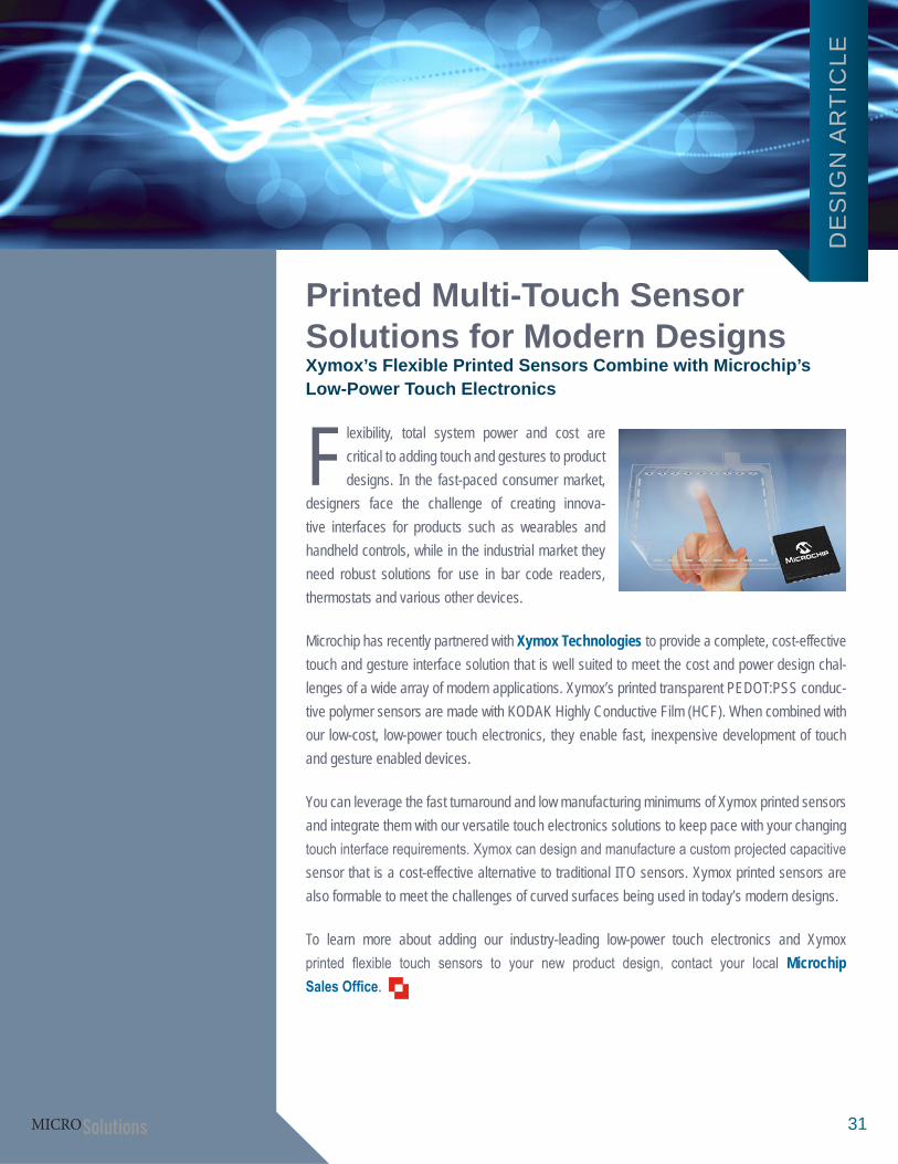
Printed Multi-Touch Sensor Solutions for Modern DesignsXymox’s Flexible Printed Sensors Combine with Microchip’s Low-Power Touch Electronics
Flexibility, total system power and cost are critical to adding touch and gestures to product designs. In the fast-paced consumer market,
designers face the challenge of creating innova-tive interfaces for products such as wearables and handheld controls, while in the industrial market they need robust solutions for use in bar code readers, thermostats and various other devices.
Microchip has recently partnered with Xymox Technologies to provide a complete, cost-effective touch and gesture interface solution that is well suited to meet the cost and power design chal-lenges of a wide array of modern applications. Xymox’s printed transparent PEDOT:PSS conduc-tive polymer sensors are made with KODAK Highly Conductive Film (HCF). When combined with our low-cost, low-power touch electronics, they enable fast, inexpensive development of touch and gesture enabled devices.
You can leverage the fast turnaround and low manufacturing minimums of Xymox printed sensors and integrate them with our versatile touch electronics solutions to keep pace with your changing touch interface requirements. Xymox can design and manufacture a custom projected capacitive sensor that is a cost-effective alternative to traditional ITO sensors. Xymox printed sensors are also formable to meet the challenges of curved surfaces being used in today’s modern designs.
To learn more about adding our industry-leading low-power touch electronics and Xymox printed flexible touch sensors to your new product design, contact your local Microchip Sales Office.

DE
SIG
N A
RT
ICLE
32
Accelerating Low-Level Code Implementation in PIC32 MCU ApplicationsThreadX® RTOS Now Supports MPLAB® Harmony Framework
Used in a huge number of products with applications in consumer electronics, medi-cal devices, industrial equipment and home
automation, Express Logic’s ThreadX RTOS is a priority-based, fully preemptive, deterministic RTOS. ThreadX provides basic system services such as preemptive and round-robin scheduling, sema-phores, message queues, mutexes, timers, interrupts and memory management. ThreadX also offers advanced features such as Preemption-Threshold™ Scheduling, Integrated Event and Downloadable Application Modules.
We are pleased to announce that the ThreadX RTOS has recently been integrated into the MPLAB Harmony Integrated Software Framework, a set of integrated building blocks that simplify and accelerate software development for our 32-bit PIC32 microcontrollers. MPLAB Harmony provides the industry’s most advanced framework of software drivers and middleware components that are easy to use and configure, and that work together in complete harmony. With this seamless integration, ThreadX for MPLAB Harmony offers you with a flexible, fully inte-grated firmware development platform for your most demanding real-time applications. You can be confident that your RTOS will be able to keep up with system events under the most extreme run-time conditions.
ThreadX for MPLAB Harmony is a high-quality, easy-to-use software framework that eliminates the bugs, hassle, and uncertainty of low-level code implementation, while improving performance and determinism. With its many features, it will help accelerate your time to market and also significantly reduce your development costs. The royalty-free, limited source version of ThreadX for MPLAB Harmony—with prices starting at $6,000—is available from microchipDIRECT.com. It is also available from Express Logic in full source code form, with license prices starting at $12,500.

EV
EN
TS
33
Connect With Us at 2015 International CES
Once again, representatives from the top consumer electronics retailers and the world’s greatest technology leaders are getting ready to converge in Las Vegas to attend the annual International CES. Microchip will be there too, with more than 30 demos on
display that span a wide range of product markets. Visit our main exhibit in Booth MP25656, South Hall 2 Meeting Place at the Las Vegas Convention Center to see our broad portfolio of innovative solutions in the automotive, computing, connectivity, Internet of Things, touch and input sensing, and wireless markets. If you'd like more in-depth information while you're at the show, you can use our Online Demo Request system to schedule an appointment to meet with representatives from Microchip and to view specific demos from these different applications areas:
Automotive Zone: Learn how our connectivity and HMI solutions contribute to the advancement of intelligence throughout the vehicle. Let our experts demonstrate our latest technologies to further enhance mobile connectivity in the car.
Computing Zone: Need computing expertise? Stop by and experience the leading innovation of Microchip’s products for computing applications.
Embedded Wireless Solutions Zone: Microchip’s wireless solutions are designed to get you to market fast, so come see us and let’s find the right wireless solution for your project.
Internet of Things (IoT) Zone: Our variety of wireless solutions, sensors and eXtreme Low Power (XLP) PIC® microcontrollers enable end-to-end solutions that help successfully connect embedded systems to the cloud and take advantage of all of the benefits of doing so.
Connectivity Zone: Stop by to learn how Microchip can enhance your mobile experience and seamlessly connect your world with our USB products.
Touch & Input Sensing Zone: Experience our award-winning solutions for 21st century input sensing—from buttons, sliders, touchpads and touch screens to three-dimensional gesture sensing. Learn how our 1-2-3D solutions can be used to enable a wide range of applications.
We’re excited to have this opportunity to meet you and demonstrate why we are a leading provider of microcontroller, mixed-signal, analog and Flash-IP solutions. See you in Las Vegas!

The Microchip name and logo and the Microchip logo are registered trademarks of Microchip Technology Incorporated in the U.S.A. and other countries.All other trademarks are the property of their registered owners. © 2014 Microchip Technology Inc. All rights reserved. 5/14DS00001746A
microchip.com/xlp
eXtreme Low Power MCUs Extend Battery Life
Low Sleep Currents with Flexible Wake-up Sources
■Sleep current down to 9 nA ■Brown-Out Reset down to 45 nA ■Real-Time Clock down to 400 nA
Low Dynamic Currents ■As low as 30 µA/MHz ■Power-effi cient execution
Large Portfolio of XLP MCUs ■8–100 pins, 4–128 KB Flash ■Wide selection of packages, including chip scale packages
Battery-Friendly Features ■Enable battery lifetime > 20 years ■Operate down to 1.8V with self write and analog functions ■Low-power supervisors for safe operation (BOR, WDT)
Flexible Peripheral Set ■ Integrated USB, LCD, RTC and touch sensing ■Eliminates costly external components