Wint er 2015 Examinations Model Answer 1 of...
23
MAHARASHTRA STATE BOARD OF TECHNICAL EDUCATION (Autonomous) (ISO/IEC-27001-2005 Certified) Winter – 2015 Examinations Subject Code: 17321 (BEE) Model Answer Page No : 1 of 23 Important Instructions to examiners: 1) The answers should be examined by key words and not as word-to-word as given in the model answer scheme. 2) The model answer and the answer written by candidate may vary but the examiner should assess the understanding level of the candidate. 3) The language errors such as grammatical, spelling errors should not be given importance (Not applicable for subject English and Communication Skills). 4) While assessing figures, examiner may give credit for principal components indicated in the figure. The figures drawn by candidate and model answer may vary. The examiner should give credit for any equivalent figure/figures drawn. 5) Credits to be given step wise for numerical problems. In some cases, the assumed constant values may vary and there may be some difference in the candidate’s answers and model answer (as long as the assumptions are not incorrect). 6) In case of some questions credit may be given by judgment on part of examiner of relevant answer based on candidate’s understanding. 7) For programming language papers, credit may be given to any other program based on equivalent concept.
Transcript of Wint er 2015 Examinations Model Answer 1 of...

MAHARASHTRA STATE BOARD OF TECHNICAL EDUCATION (Autonomous)
(ISO/IEC-27001-2005 Certified)
Winter – 2015 Examinations
Subject Code: 17321 (BEE) Model Answer Page No : 1 of 23
Important Instructions to examiners:
1) The answers should be examined by key words and not as word-to-word as given in the model
answer scheme.
2) The model answer and the answer written by candidate may vary but the examiner should assess
the understanding level of the candidate.
3) The language errors such as grammatical, spelling errors should not be given importance (Not
applicable for subject English and Communication Skills).
4) While assessing figures, examiner may give credit for principal components indicated in the figure.
The figures drawn by candidate and model answer may vary. The examiner should give credit for
any equivalent figure/figures drawn.
5) Credits to be given step wise for numerical problems. In some cases, the assumed constant values
may vary and there may be some difference in the candidate’s answers and model answer (as long
as the assumptions are not incorrect).
6) In case of some questions credit may be given by judgment on part of examiner of relevant answer
based on candidate’s understanding.
7) For programming language papers, credit may be given to any other program based on equivalent
concept.

MAHARASHTRA STATE BOARD OF TECHNICAL EDUCATION (Autonomous)
(ISO/IEC-27001-2005 Certified)
Winter – 2015 Examinations
Subject Code: 17321 (BEE) Model Answer Page No : 2 of 23
1 A) Attempt any six: 12
1 A) a) Give two examples of trivalent and pentavalent impurities. 2
Ans: Trivalent Impurities: (any two)
1) Gallium (Ga) 2) Indium (In) 3) Aluminium (Al) 4) Boron (B)
Pentavalent Impurities: (any two) 1) Phosphorus (P) 2) Antimony (Sb) 3) Arsenic (As) 4) Bismuth (Bi)
½ mark each
1 A) b) Draw the symbol of LED and photodiode. 2
Ans: 1) LED:
2) Photodiode:
1 mark
1 mark
1 A) c) Define and of the transistor. 2
Ans: 1) :
It is defined as the ratio of collector current (IC) to emitter current (IE).
α =IC
IE
2) : It is defined as the ratio of collector current (IC) to base current (IB).
β =IC
IB
1 mark
1 mark
1 A) d) State the need of biasing of BJT. 2
MAHARASHTRA STATE BOARD OF TECHNICAL EDUCATION (Autonomous)
(ISO/IEC-27001-2005 Certified)
Winter – 2015 Examinations
Subject Code: 17321 (BEE) Model Answer Page No : 3 of 23
Ans: Need of Biasing of BJT: The purpose of dc biasing of BJT is to obtain a certain dc collector current at a certain dc collector voltage i.e. IC and VCE (Q-point). The selected Q point is stabilized against variation in temperature.
2 marks
1 A) e) List two types of oscillator, which generates frequency in RF range. 2
Ans: Types of Oscillators generating frequencies in RF range:
i) Hartley Oscillator ii) Colpitt’s Oscillator iii) Clapp Oscillator
1 mark each of any
two
1 A) f) State two advantages of digital circuits. 2
Ans: Advantages of Digital Circuits:
i) Digital circuits are easier to design. ii) Information storage is easy. iii) Accuracy and precision are greater. iv) Less affected by noise. v) Reliability is more.
1 mark each of any
two
1 A) g) Write down output voltage for IC’s 7818 and IC’s 7924. 2
Ans: i) For IC 7818, output voltage is +18 volt. ii) For IC 7924, output voltage is -24 volt.
1 mark each
1 A) h) State any two applications of zener diode. 2
Ans: Applications of Zener Diode:
i) As a voltage regulator. ii) As a fixed reference voltage provider in transistor biasing circuits. iii) As peak clippers or limiters in wave shaping circuits.
1 mark each of any
two
1 B) Attempt any two: 8
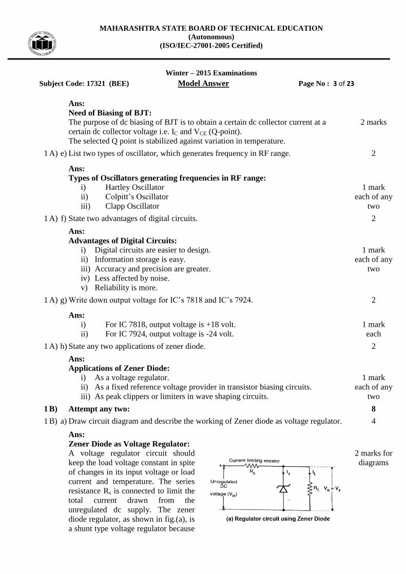
1 B) a) Draw circuit diagram and describe the working of Zener diode as voltage regulator. 4
Ans: Zener Diode as Voltage Regulator: A voltage regulator circuit should keep the load voltage constant in spite of changes in its input voltage or load current and temperature. The series resistance Rs is connected to limit the total current drawn from the unregulated dc supply. The zener diode regulator, as shown in fig.(a), is a shunt type voltage regulator because
2 marks for diagrams

MAHARASHTRA STATE BOARD OF TECHNICAL EDUCATION (Autonomous)
(ISO/IEC-27001-2005 Certified)
Winter – 2015 Examinations
Subject Code: 17321 (BEE) Model Answer Page No : 4 of 23
the control element i.e. zener diode is connected in parallel with the load resistance. Working of Zener Voltage Regulator: The input voltage Vin is an unregulated dc voltage which is obtained from a rectifier filter combination. Rs is the current limiting resistor and RL is the load resistor. The input voltage Vin should always be higher than the breakdown voltage VZ. The zener diode is reverse biased and operates in the zener region of the reverse characteristics, as shown in fig.(b) If Vin is higher than VZ and if the Zener current IZ is between IZmin and IZmax then the voltage across the Zener will remain constant equal to VZ irrespective of any changes in Vin and IL. As the output voltage is constant and equal to VZ, we get regulated output voltage. The Zener current IZ should not be higher than IZmax, otherwise excessive power dissipation will damage the Zener diode. The Zener current IZ should not be less than IZmin because the Zener diode then cannot operate in the zener region and cannot maintain constant voltage across it. The regulator keeps the load voltage constant in spite of changes in input voltage and load current.
2 marks for explanation
1 B) b) Explain construction and working principle of LED. 4
Ans: Construction of LED: The basic structure of LED is shown in fig.(a). The active region exists between the p and n regions. The light emerges from the active side in all the directions when electron hole-pairs recombine. The disadvantage of this structure is that the LED emits light in all the directions. This problem is solved by placing the basic structure inside a small reflective cup so as to focus the light in the desired direction. Such a structure is called as a cup type construction and is shown in fig.(b). Working Principle of LED: When the LED is forward biased, the electrons in the n-region will cross the junction and recombine with the holes in the p-type material. These free electrons reside in the conduction band and hence at a higher energy level than the holes in the valance band. When the recombination takes place, these electrons return back to the valance band which is at lower
2 marks for diagram
2 marks for explanation

MAHARASHTRA STATE BOARD OF TECHNICAL EDUCATION (Autonomous)
(ISO/IEC-27001-2005 Certified)
Winter – 2015 Examinations
Subject Code: 17321 (BEE) Model Answer Page No : 5 of 23
energy level than the conduction band. While returning back, the recombining electrons give away the excess energy in the form of light. This process is called as “electroluminescence”, shown
in fig.(c). In this way an LED emits light. This is the principle of operation of LED.
1 B) c) Draw output characteristic of CE configuration and show various region. 4
Ans: Output characteristic of CE configuration:
2 marks for diagram
2 marks for showing regions
2 Attempt any Four: 16
2 a) Draw the circuit diagram of bridge rectifier with filter. Explain operation with I/P and O/P waveform.
4
Ans: Bridge rectifier with filter: The circuit arrangement of bridge type rectifier with type filter is shown in fig.(a). The -filter is a combination of shunt capacitor filter and series L-filter. Due to the use of three filtering elements, the ripple factor of the filter is very low.
Operation: During positive half-cycle of input, the secondary voltage VAB is positive, which
1 mark for circuit
diagram

MAHARASHTRA STATE BOARD OF TECHNICAL EDUCATION (Autonomous)
(ISO/IEC-27001-2005 Certified)
Winter – 2015 Examinations
Subject Code: 17321 (BEE) Model Answer Page No : 6 of 23
makes diodes D1 and D2 forward biased and D3 and D4 reverse biased. The load current flows from terminal A through D1, L, RL, D2 to terminal B. The load voltage and load current are positive. During negative half-cycle of input, the secondary voltage VAB becomes negative, i.e.VBA is positive, which makes diodes D3 and D4 forward biased and D1 and D2 reverse biased. The load current flows from terminal B through D3, L, RL, D4 to terminal A. The load voltage and load current are once again positive. The output of bridge rectifier is full wave rectified pulsating DC. The ripples in the current are reduced by filter inductor and the ripples in voltage are reduced by filter capacitors. Thus the pulsating DC is smoothened by filter and smooth DC voltage appears across the load. The input and output waveforms are shown in the figure.
2 marks for explanation
1 mark for waveforms
2 b) Explain single stage CE amplifier with the help of circuit diagram. 4
Ans: Single-stage CE Amplifier:
The capacitors C1 and C2 are called as the coupling capacitors. As the load resistor RL (not shown in the diagram) is coupled to the amplifier through the coupling capacitor, this amplifier is called as RC coupled amplifier. The transistor is connected in the common emitter (CE) configuration. Therefore, this amplifier is called CE amplifier.
2 marks for circuit
diagram
2 marks for explanation
2 c) Draw diagram of class A push-pull amplifier and explain its operation. 4
Ans: Class A Push-pull Amplifier: The circuit diagram of class A push-pull amplifier is as shown in the fig.(a). Operation: The resistors R1 and R2 along with Vcc provide the dc biasing so as to keep the operating point (Q-point) at the centre of the dc load line, in order to achieve the class A operation. The driver transformer provides the phase splitting function and produces two voltages Va1 and Va2 which are equal in magnitude but 180 out of phase. The Vcc is applied to the collectors of transistors Q1 and Q2 through the centre-tapped output transformer.

MAHARASHTRA STATE BOARD OF TECHNICAL EDUCATION (Autonomous)
(ISO/IEC-27001-2005 Certified)
Winter – 2015 Examinations
Subject Code: 17321 (BEE) Model Answer Page No : 7 of 23
Operation Under dc conditions: The transistors Q1 and Q2 have identical characteristics. Therefore their dc collector currents ic1 and ic2 are equal. These currents will flow in opposite directions through the two halves of the primary windings of the output transformer. Therefore, there is cancellation of flux produced due to dc current and saturation of the transformer core is avoided. For complete cancellation of flux, it is essential that the two transistors are perfectly matched. Operation Under ac conditions: In the positive half cycle of input voltage Vs, the secondary voltage Vs1 will be positive while Vs2 will be negative, as shown in fig.(b). Therefore, transistor Q1 is more forward biased while Q2 is less forward biased. Therefore, ic1 will increase and ic2 will decrease. The output current iL is proportional to the difference between ic1 and ic2.
iL =N1
N2(ic1 − ic2) where,
N1
N2 is the turns ratio of the output transformer.
Therefore in the positive half cycle of Vs, the output current will be positive. As the load is resistive, the load current will be in phase with the load voltage.
VL = iLR =N1
N2
(ic1 − ic2)R
Therefore load voltage will be positive.
In the negative half cycle of input voltage Vs, the secondary voltage Vs1 will be negative while Vs2 will be positive, as shown in fig.(c). Therefore, transistor Q2 will be more forward biased while Q2 will be less forward biased. Therefore, ic1 will decrease and ic2 will increase. The output current iL is proportional to the difference between ic1 and ic2 and hence becomes negative. The load voltage, being in phase with load current, will also become negative.
1 mark for diagram
3 marks for explanation

MAHARASHTRA STATE BOARD OF TECHNICAL EDUCATION (Autonomous)
(ISO/IEC-27001-2005 Certified)
Winter – 2015 Examinations
Subject Code: 17321 (BEE) Model Answer Page No : 8 of 23
2 d) Classify rectifier and filter. 4
Ans: Classification of Rectifier:
Classification of Filters:
2 marks
2 marks
2 e) Explain construction and working principle of NPN transistor. 4
Ans: Construction of NPN transistor: A transistor is formed of two p-n junctions. For unbiased p-n junctions, the depletion regions are formed. The fig.(a) shows the depletion regions formed at the B-E and C-B junctions of n-p-n transistor.
Working Principle: When the n-p-n transistor is biased, as shown in fig.(b), such that the emitter-base junction is forward biased and collector-base junction is reverse biased, the
1 mark for constructio
n

MAHARASHTRA STATE BOARD OF TECHNICAL EDUCATION (Autonomous)
(ISO/IEC-27001-2005 Certified)
Winter – 2015 Examinations
Subject Code: 17321 (BEE) Model Answer Page No : 9 of 23
minority and majority carriers are set into the motion. The majority carriers electrons from n-region enters into p-region and holes from p-region enters into n-region. Since the base is lightly doped than the emitter, almost all the current flowing across the B-E junction consists of electrons entering the base from the emitter. Hence the electrons are the majority carriers in n-p-n transistor.
Some of the electrons entering into the base region do not reach the collector region. Instead they flow out of the base terminal via the base connection as shown in fig.(c) due to recombination. As the base region is very thin and lightly doped, there are very few holes available in the base region for recombination. Hence about 2% electrons will flow out of base due to recombination. The remaining 98% electrons cross the reverse biased collector-base junction to constitute the collector current. They cross the collector region and collected by the supply Vcc. The emitter current is thus equal to the sum of the base current and collector current. 𝐼𝐸 = 𝐼𝐵 + 𝐼𝐶
3 marks for working principle
2 f) A multistage amplifier is consisting of three stages, each having gain of 10. What is the overall voltage gain in dB?
4
Ans: Data given: Three stage amplifier Gains: Av1 = Av2 = Av3 = 10 Over-all gain = Av1 Av2 Av3 = 101010 = 1000 Over-all gain in dB = 20 log10(1000) = 60 dB
OR Av1 = 20 log10(10) = 20 dB Av2 = Av3 = 20 log10(10) = 20 dB Over-all gain in dB = Av1 + Av2 +Av3 = 20+20+20 = 60 dB.
Stepwise solution 4 marks
3 Attempt any Four: 16

MAHARASHTRA STATE BOARD OF TECHNICAL EDUCATION (Autonomous)
(ISO/IEC-27001-2005 Certified)
Winter – 2015 Examinations
Subject Code: 17321 (BEE) Model Answer Page No : 10 of 23
3 a) Compare CB, CE and CC configurations on the basis of i) Input impedance ii) Current gain iii) Voltage gain iv) Output impedance
4
Ans: Comparison between CB, CE and CC configurations:
Parameter CB CE CC Input Impedance Low
Or 50
Medium Or
600 to 4k
High Or
1 M Current Gain Less than or equal
to 1 Or
𝛼 =𝐼𝐶
𝐼𝐸
High Or
𝛽 =𝐼𝐶
𝐼𝐵
High Or
𝛾 =𝐼𝐸
𝐼𝐵
Voltage Gain Medium Medium Less than or equal to 1
Output Impedance High Or
50 k
Medium Or
10 k to 50 k
Low Or
50
1 mark for each point
3 b) Derive the relation between and with to BJT. 4
Ans: Relation between and : Current gain of transistor in CB configuration is ,
𝛼 =𝐼𝐶
𝐼𝐸
But 𝐼𝐸 = 𝐼𝐵 + 𝐼𝐶
𝛼 =𝐼𝐶
𝐼𝐵 + 𝐼𝐶
Dividing numerator and denominator by IB,
𝛼 =
𝐼𝐶
𝐼𝐵
1 +𝐼𝐶
𝐼𝐵
But 𝛽 =𝐼𝐶
𝐼𝐵 the current gain of transistor in CE configuration.
Therefore,
𝜶 =𝜷
𝟏 + 𝜷
OR
Current gain of transistor in CE configuration is ,
𝛽 =𝐼𝐶
𝐼𝐵
Stepwise derivation 4 marks

MAHARASHTRA STATE BOARD OF TECHNICAL EDUCATION (Autonomous)
(ISO/IEC-27001-2005 Certified)
Winter – 2015 Examinations
Subject Code: 17321 (BEE) Model Answer Page No : 11 of 23
But 𝐼𝐸 = 𝐼𝐵 + 𝐼𝐶, so 𝐼𝐵 = 𝐼𝐸 − 𝐼𝐶
𝛽 =𝐼𝐶
𝐼𝐸 − 𝐼𝐶
Dividing numerator and denominator by IE,
𝛽 =
𝐼𝐶
𝐼𝐸
1 −𝐼𝐶
𝐼𝐸
But 𝛼 =𝐼𝐶
𝐼𝐸 the current gain of transistor in CE configuration.
Therefore,
𝜷 =𝜶
𝟏 − 𝜶
Stepwise derivation 4 marks
3 c) Draw and explain the characteristic of UJT. 4
Ans: UJT Characteristics:
The UJT characteristic is emitter voltage versus emitter current characteristic, as shown in the figure. For emitter voltages less than VP (peak point voltage) the UJT is in the off state and magnitude of IE is not greater than IEO. The emitter current IEO corresponds very closely with the reverse leakage current ICO of a bipolar transistor. This region is known as the cut off region. As the emitter voltage increases and reaches VP = ( VBB+VD), the UJT starts conducting. Then with increase in emitter IE the emitter voltage decreases as shown. The reduction in voltage across UJT is due to the drop in resistance RB1 with increase in the value of IE. This region of operation is known as a “Negative
Resistance” region, which is stable enough to be used in various applications.
Eventually the “valley point” will be reached and further increase in IE will place the device into saturation.
2 marks for diagram
with labels
2 marks for explanation
3 d) Define load regulation and line regulation for regulated power supply with expression.
4
Ans: Load Regulation: It is defined as the change in output voltage expressed as fraction of full load output
2 marks for

MAHARASHTRA STATE BOARD OF TECHNICAL EDUCATION (Autonomous)
(ISO/IEC-27001-2005 Certified)
Winter – 2015 Examinations
Subject Code: 17321 (BEE) Model Answer Page No : 12 of 23
voltage when the load current is changed from zero (no load) to full load value.
Load Regulation =𝑉𝑁𝐿−𝑉𝐹𝐿
𝑉𝐹𝐿 with Vin constant
%Load Regulation =𝑉𝑁𝐿−𝑉𝐹𝐿
𝑉𝐹𝐿× 100
where, VNL is the no load output voltage, VFL is the full load output voltage Line Regulation: It is defined as the change in output voltage due to change in input voltage with load RL constant (IL constant)
%Line Regulation =∆𝑉𝑂×100
𝑉𝑂 with RL constant or IL constant.
where, 𝑉𝑂 is the output voltage. OR
Line Regulation= 𝑉𝐿𝐻 − 𝑉𝐿𝐿 where, VLH is the load voltage with high line voltage, VLL is the load voltage with low line voltage
definitions
2 marks for expressions
3 e) Write important features of IC 723. 4
Ans: Important features of IC 723:
i) It can be connected to function as a positive or negative voltage regulator with an output voltage ranging from 2V to 37V.
ii) Output current can be up to 150 mA. iii) The maximum supply voltage is 40V. iv) The line and load regulations are each 0.01%. v) Built-in short circuit protection. vi) Very low temperature drift. vii) High ripple rejection.
1 mark for each of any
four features
3 f) Draw and explain the construction of n-channel JFET (FET) 4
Ans: N-channel JFET (FET):
Construction: The n-channel JFET has n-type semiconductor used as a channel which has two terminals, drain and source. Two p-type semiconductors are attached at both sides of n-channel and forms third terminal gate. Thus pn junction exists between gate
2 marks for diagram
2 marks for explanation

MAHARASHTRA STATE BOARD OF TECHNICAL EDUCATION (Autonomous)
(ISO/IEC-27001-2005 Certified)
Winter – 2015 Examinations
Subject Code: 17321 (BEE) Model Answer Page No : 13 of 23
and source. 1) When VGS = 0 volt:
When a voltage is applied between the drain and source with a DC supply voltage VDD with VGS = 0 V, the electrons flow from source to drain through the narrow channel existing between the depletion regions. This constitutes drain current ID. The value of drain current is maximum when VGS = 0 V. This current is designated vy the symbol IDSS.
2) When VGS is negative: When VGS is increased below zero i.e negative, the reverse voltage across the gate source junction is incrased. As a result depletion regions are widened. This reduces effective width of channe and therefore controls the flow of drain current through the channel. If VGS is increased further, two depletion regions touch each other. The drain current reduces to zero. The gate to source voltage at which current reduces to zero is called as pinch-off voltage.
4 Attempt any Four: 16
4 a) Draw the circuit diagram of RC phase shift oscillator. Write working in steps. Give the formula of frequency of oscillation.
4
Ans: RC Phase shift Oscillator:
1) Circuit Diagram: 2) Working:
In RC phase shift oscillator, CE amplifier is used, which provides 180 phase shift between input and output.
In feedback network, three RC phase shift networks are used in which each network provides 60 phase shift, so that total phase shift is 180.
The total phase shift around whole circuit is 360.
So circuit gets positive feedback and works as an oscillator.
3) Frequency of Oscillations:
𝑓𝑐 =1
2𝜋𝑅𝐶√6
2 marks for circuit
diagram
1 mark for working
1 mark
4 b) In a Colpitt’s oscillator, C1 = 0.2 F and C2 = 0.02 F. If the frequency of oscillation is 10kHz, find the value of inductor. Also find the required gain for the oscillation.
4
Ans: Data Given: C1 = 0.2 F C2 = 0.02 F fc = 10 kHz = 10103 Hz. To find out: Value of inductor (L) and Gain (A)
1) To find Inductor L:

MAHARASHTRA STATE BOARD OF TECHNICAL EDUCATION (Autonomous)
(ISO/IEC-27001-2005 Certified)
Winter – 2015 Examinations
Subject Code: 17321 (BEE) Model Answer Page No : 14 of 23
In Colpitt’s oscillator,
𝑓𝑐 =1
2𝜋√𝐿𝐶𝑇… … … … … … … … … … … . . (𝑖)
where, 𝐶𝑇 =𝐶1𝐶2
𝐶1+𝐶2=
0.2×0.02
0.2+0.02=
0.004
0.22= 0.018𝜇𝐹
Substituting CT and fc into eq.(i),
10 × 103 =1
2𝜋√𝐿(0.018×10⁻⁶)
Squaring both sides,
𝐿 =1
4𝜋2 × 100 × 106 × 0.018 × 10−6
=1
4𝜋2×1.8=
1
70.99
= 0.01408 = 14 × 10−3
𝑳 = 𝟏𝟒 𝒎𝑯 2) To find A:
In Colpitt’s oscillator,
A > 𝐶1
𝐶2
A > 0.2
0.02
Gain A > 10.
1 mark
1 mark
1 mark
1 mark
4 c) Convert the following decimal number into equivalent binary number. i) 63.92 ii) 109
4
Ans: 1) (63.92)10 = ( ? )2
For integer part 63:
2 63 2 31 1 LSB 2 15 1 2 7 1 2 3 1 2 1 1 0 1 MSB
(63)10 = (111111)2 For fractional part:
0.922 = 1.84 1 MSB 0.922 = 1.68 1 0.922 = 1.36 1 0.922 = 0.72 0 0.922 = 1.44 1 LSB
(.92)10 = (.11101)2 (63.92)10 = (111111.11101)2
1 mark
1 mark

MAHARASHTRA STATE BOARD OF TECHNICAL EDUCATION (Autonomous)
(ISO/IEC-27001-2005 Certified)
Winter – 2015 Examinations
Subject Code: 17321 (BEE) Model Answer Page No : 15 of 23
2) (109)10 = ( ? )2
2 109 2 54 1 LSB 2 27 0 2 13 1 2 6 1 2 3 0 2 1 1 0 1 MSB
(109)10 = (1101101)2
2 marks
4 d) Draw the symbol, logic expression and truth table for two input of the following gates: i) AND gate ii) OR gate.
4
Ans: i) AND gate:
Logical expression: Y = AB Truth Table:
A B Y= AB 0 0 0 0 1 0 1 0 0 1 1 1
ii) OR gate:
Logical expression: Y = A+B Truth Table:
A B Y= A+B 0 0 0 0 1 1 1 0 1 1 1 1
1 mark for symbol
1 mark for logical
expression and truth
table
1 mark for symbol
1 mark for logical
expression and truth
table
4 e) Draw and explain the O/P characteristic of JFET (FET). 4
Ans: Output Characteristics of JFET: The output characteristics of JFET is plotted between the drain current ID and
drain to source voltage VDS for constant gate to source voltage VGS. When VGS = 0 volt constant, if we increase VDS , the drain current ID increases
proportionally and remains constant after particular value of VDS. This drain to source voltage is called pinch-off voltage VP. This constant drain current is maximum current flowing through the JFET and known as source saturation current IDSS.
When we increase reverse bias on gate to source junction, the drain current
2 marks for explanation

MAHARASHTRA STATE BOARD OF TECHNICAL EDUCATION (Autonomous)
(ISO/IEC-27001-2005 Certified)
Winter – 2015 Examinations
Subject Code: 17321 (BEE) Model Answer Page No : 16 of 23
decreases. When the reverse bias VGS is increased beyond certain value, the drain current
becomes zero. This gate-source voltage is known as VGS(Off).
2 marks for diagram
4 f) Compare Hartley and Colpitt’s oscillator. 4
Ans: Comparison between Hartley and Colpitt’s oscillator:
Particulars Hartley Oscillator Colpitt’s Oscillator 1) Type of
oscillator It is a LC type of oscillator It is a LC type of oscillator
2) Components used
Two inductors and one capacitor are used in tank circuit.
Two capacitors and one inductor are used in tank circuit.
3) Frequency of oscillation
𝑓𝑐 =1
2𝜋√𝐿𝑇𝐶
𝐿𝑇 = 𝐿1 + 𝐿2
𝑓𝑐 =1
2𝜋√𝐿𝐶𝑇
𝐶𝑇 =𝐶1 × 𝐶2
𝐶1 + 𝐶2
4) Advantages Suitable at high frequencies
Small size Low cost
Suitable at high frequencies Small size Low cost
5) Disadvantages
Poor frequency stability Poor frequency stability
5 Attempt any Four: 16
5 a) For a PN junction diode applied voltage are 0v, +5v, -10v. Draw the PN junction indicating relative width of the depletion region in each.
4
Ans:

MAHARASHTRA STATE BOARD OF TECHNICAL EDUCATION (Autonomous)
(ISO/IEC-27001-2005 Certified)
Winter – 2015 Examinations
Subject Code: 17321 (BEE) Model Answer Page No : 17 of 23
Relative Width of Depletion Region: i) For 0 V:
Depletion region width is comparatively small.
ii) For 5 V:
Diode is forward biased and conducting, hence depletion region is absent.
iii) For -10 V: Diode is reverse biased, the width of depletion region is increased.
1 mark
1 mark
2 marks
5 b) A full wave rectifier uses two diodes, the internal resistance of each diode may be assumed constant at 20. The transformer r.m.s. secondary voltage from centre tap to each end of secondary is 50 V and load resistance is 980 . Find:
i) the mean load current ii) the rms value of load current
4
Ans: Data Given: Vrms = 50V RL = 980 RS = 20 To find out: Idc = ? Irms = ?

MAHARASHTRA STATE BOARD OF TECHNICAL EDUCATION (Autonomous)
(ISO/IEC-27001-2005 Certified)
Winter – 2015 Examinations
Subject Code: 17321 (BEE) Model Answer Page No : 18 of 23
In full-wave centre tap rectifier,
𝑉𝑟𝑚𝑠 =𝑉𝑚
√2
∴ 𝑉𝑚 = √2 × 𝑉𝑟𝑚𝑠 = √2 × 50 ∴ 𝑽𝒎 = 𝟕𝟎. 𝟕𝟏 𝑽
Now the peak load current is given by, 𝐼𝑚 =𝑉𝑚
[𝑅𝑆+𝑅𝐿]=
70.71
20+980= 0.0707 𝐴
∴ 𝑰𝒎 = 𝟕𝟎. 𝟕 𝒎𝑨 The mean load current is given by,
𝐼𝑑𝑐 =2𝐼𝑚
𝜋=
70.7 × 2
3.142
𝑰𝒅𝒄 = 𝟒𝟓. 𝟎𝟑 𝒎𝑨 The rms load current is given by,
𝐼𝑟𝑚𝑠 =𝐼𝑚
√2=
70.7
√2
𝑰𝒓𝒎𝒔 = 𝟓𝟎. 𝟏𝟒 𝒎𝑨
1 mark
1 mark
1 mark
1 mark
5 c) List the type of biasing circuit. Draw the diagram of voltage divider bias method and describe its operation.
4
Ans: Types of Biasing Circuits:
i) Base bias (Fixed bias) ii) Base bias with emitter feedback (Emitter feedback bias) iii) Base bias with collector feedback (Collector feedback bias) iv) Voltage divider bias (Self bias) v) Emitter bias
Voltage Divider Bias: R1, R2 and RE are biasing resistors and VCC is biasing voltage. Voltage at base of transistor is
𝑉𝐵 =𝑅2
𝑅1 + 𝑅2𝑉𝐶𝐶
Applying KVL at input circuit, 𝑉𝐵 − 𝑉𝐵𝐸 − 𝑉𝐸 = 0
Since VBE is very small 𝑉𝐵 = 𝑉𝐸
Now, 𝐼𝐸 =𝑉𝐸
𝑅𝐸
∴ 𝐼𝐶 =𝑉𝐸
𝑅𝐸 [𝑠𝑖𝑛𝑐𝑒 𝐼𝐶 ≅ 𝐼𝐸]
Applying KVL to output circuit, 𝑉𝐶𝐶 − 𝐼𝐶𝑅𝐶 − 𝑉𝐶𝐸 − 𝑉𝐸 = 0
𝑉𝐶𝐶 − 𝐼𝐶𝑅𝐶 − 𝑉𝐶𝐸−𝐼𝐸𝑅𝐸 = 0 𝑉𝐶𝐸 = 𝑉𝐶𝐶 − 𝐼𝐸(𝑅𝐶 + 𝑅𝐸) [𝑠𝑖𝑛𝑐𝑒 𝐼𝐶 ≅ 𝐼𝐸]
5 d) Draw two stage RC coupled amplifier and draw its frequency response. Show the bandwidth.
4

MAHARASHTRA STATE BOARD OF TECHNICAL EDUCATION (Autonomous)
(ISO/IEC-27001-2005 Certified)
Winter – 2015 Examinations
Subject Code: 17321 (BEE) Model Answer Page No : 19 of 23
Ans:
2 marks for circuit
diagram
1 marks for frequency response
plot
1 mark for bandwidth
5 e) Compare transformer coupled amplifier with RC coupled amplifier. 4
Ans: Particulars RC Coupled Amplifier Transformer Coupled
Amplifier 1) Size Small Comparatively large and
bulky 2) Cost Low Comparatively costly 3) Frequency
Response Excellent in audio frequency range
Poor
4) Impedance matching
Not good Excellent
5) Applications Voltage amplification Power amplification
1 mark for each of any four points
5 f) Compare JFET with MOSFET. 4
Ans: Particulars JFET MOSFET
1) Type Voltage controlled device Voltage controlled device 2) Mode of
operation Operates only in depletion mode
Operates in depletion and enhancement mode
3) Input impedance
Higher Higher than JFET
1 mark for each of any four points

MAHARASHTRA STATE BOARD OF TECHNICAL EDUCATION (Autonomous)
(ISO/IEC-27001-2005 Certified)
Winter – 2015 Examinations
Subject Code: 17321 (BEE) Model Answer Page No : 20 of 23
4) Characteristic curve
More flat Less flat than FET
5) Gate to source junction
Only reverse bias Forward or reverse bias
6) Gate connection
Not isolated from substrate Isolated by SiO2 layer from substrate
(Examiner may consider any other points of comparison during evaluation)
6 Attempt any Four: 16
6 a) Describe transistor as a switch with neat diagram. 4
Ans: Transistor as Switch: A transistor can be used for two types of applications viz. amplification and switching. For amplification, the transistor is biased in its active region. For switching applications, transistor is biased to operate in the saturation (full on) or cut-off (full off) region.
(i) Transistor in cut-off region (Open switch):
In the cur-off region, both the junctions of transistor are reverse biased and very small reverse current flows through the transistor. The voltage drop across the transistor (VCE) is high, nearly equal to supply voltage VCC. Thus, in cut-off region the transistor is equivalent to an open switch as shown in fig.(a).
(ii) Transistor in Saturation region (Closed switch):
When Vin is positive, a large base current flows and transistor saturates. In the saturation region, both the junctions of transistor are forward biased. The collector current is very large, the voltage drop across the transistor (VCE) is very small, of the order of 0.2V to 1 V, depending on
1 mark for diagram
1 mark for explanation
1 mark for diagram
1 mark for explanation
MAHARASHTRA STATE BOARD OF TECHNICAL EDUCATION (Autonomous)
(ISO/IEC-27001-2005 Certified)
Winter – 2015 Examinations
Subject Code: 17321 (BEE) Model Answer Page No : 21 of 23
the type of transistor. Thus in saturation region, the transistor is equivalent to a closed switch.
6 b) Define: i) Drain resistance ii) Transconductance iii) Amplification factor iv) Pinch off voltage of FET.
4
Ans: i) Drain Resistance:
(a) DC drain resistance, also known as static or ohmic resistance of
channel, is expressed as, 𝑅𝐷𝑆 =𝑉𝐷𝑆
𝐼𝐷
(b) AC drain resistance, also known as dynamic resistance of channel, is defined as resistance between drain to source when JFET is operating in pinch-off or saturation region and expressed as,
𝑟𝑑 =∆𝑉𝐷𝑆
∆𝐼𝐷
ii) Transconductance: It is also known as forward transconductance (gm). It is the ratio of small change in drain current to corresponding change in gate to source voltage.
𝑔𝑚 =∆𝐼𝐷
∆𝑉𝐺𝑆 , keeping VDS constant.
iii) Amplification Factor: It is defined as the ratio of small change in drain voltage to small change in gate voltage at constant drain current.
Amplification factor =∆𝑉𝐷𝑆
∆𝑉𝐺𝑆 , keeping ID constant.
iv) Pinch-off Voltage: It is the value of the drain to source voltage VDS at which the drain current ID reaches its constant saturation value. Any further increase in VDS does not have any effect on the value of ID. It is denoted by VP.
1 mark for each
correct definition
6 c) Draw transistorized series regulator and explain its working. 4
Ans: Transistorized Series Regulator: The figure shows a circuit of a transistor series regulator. Since the transistor is connected in series with the load, the circuit is known as a series regulator. Operation:
i) The unregulated DC supply is fed to the input terminal as shown in the figure.
ii) The output voltage is given by VL = VZ - VBE iii) VZ being a zener voltage, can assumed constant. Therefore, if the output
voltage varies, the VBE changes. iv) If the output voltage increases due to some reason, then VBE decreases
and due to this base current decreases. Therefore the collector current decreases.
2 marks for operation

MAHARASHTRA STATE BOARD OF TECHNICAL EDUCATION (Autonomous)
(ISO/IEC-27001-2005 Certified)
Winter – 2015 Examinations
Subject Code: 17321 (BEE) Model Answer Page No : 22 of 23
v) This will increase the collector to emitter voltage (VCE) across the transistor and VL will be regulated, as VL = VS - VCE
vi) If the output voltage decreases, then exactly opposite action will take place and the output voltage is regulated.
vii) The circuit action may be summarized in the form of following equation. VL VBE IB IC VCE VL
2 marks for circuit
diagram
6 d) Draw the block diagram for DC power supply; explain the function of each block. 4
Ans: DC Power Supply: There are four basic blocks of a DC regulated power supply. They are:
1) Step-down transformer 2) Rectifier 3) Filter 4) Voltage Regulator
Functions of Each Block:
i) Step-down transformer: Reduces 230V, 50 hz ac voltage to required ac voltage level.
ii) Rectifier: Converts ac voltage into dc voltage. Typically bridge type full-wave rectifier is widely used.
iii) Filter: Used to remove fluctuations (ripples) present in dc output. iv) Voltage regulator: Provides constant dc output voltage irrespective of
changes in load current or changes in input voltage. Voltage divider circuit is used to provide different dc voltages required for different electronic circuits.

MAHARASHTRA STATE BOARD OF TECHNICAL EDUCATION (Autonomous)
(ISO/IEC-27001-2005 Certified)
Winter – 2015 Examinations
Subject Code: 17321 (BEE) Model Answer Page No : 23 of 23
6 e) Write advantages and disadvantages of positive and negative feedback. 4
Ans: Advantages of Positive Feedback:
i) Voltage gain increases. ii) No phase shift is provided. iii) Feedback signal and input signal are in phase. iv) Input and Output voltage increases.
Disadvantages of Positive Feedback: i) Stability becomes poor as feedback increases. ii) Noise increases with feedback. iii) Bandwidth decreases. iv) Input impedance decreases.
Advantages of Negative Feedback: i) Stability becomes better as feedback increases. ii) Noise decreases with feedback. iii) Bandwidth increases. iv) Input impedance increases.
Disadvantages of Negative Feedback: i) Voltage gain decreases.
Phase shift of 180 is provided. ii) Feedback signal and input signal are out of phase. iii) Input and Output voltage decreases.
6 f) a) Define junction field effect transistor (JFET) and give an example. 2
Ans: Junction Field-Effect Transistor: It is a semiconductor device having three terminals, namely Gate, Drain and Source, in which the current flow is controlled by an electric field set up by an external voltage applied to gate terminal. Types of JFET are: i) n-channel JFET and ii) p-channel JFET Examples of JFET: BFW 10, BFW 11
1 mark for definition
1 mark for example
6 f) b) Convert (AFB2)16 to Binary number. 2
Ans: Hexadecimal Number
A F B 2 1010 1111 1011 0010
(AFB2)16 = (1010 1111 1011 0010)2
1mark for step
1 mark for final ans