Wafer Scale Mapping and Statistical Analysis of Radio ...
6
FULL PAPER 1800711 (1 of 6) © 2019 WILEY-VCH Verlag GmbH & Co. KGaA, Weinheim www.advelectronicmat.de Wafer Scale Mapping and Statistical Analysis of Radio Frequency Characteristics in Highly Uniform CVD Graphene Transistors Mengchuan Tian, Ben Hu, Haifang Yang, Chengchun Tang, Mengfei Wang, Qingguo Gao, Xiong Xiong, Zhenfeng Zhang, Tiaoyang Li, Xuefei Li, Changzhi Gu, and Yanqing Wu* DOI: 10.1002/aelm.201800711 electrical performance from individual or few devices and wafer-scale uniformity analysis is still lacking. Up to now, a few reported complex graphene RF circuits utilized several graphene devices with sim- ilar electrical properties. For instance, Han et al. reported a graphene RF receiver inte- grated circuit consisting of three graphene RF devices. [7] Lyu et al. also demonstrated a double-balanced graphene gate-pumped resistive mixer integrated circuit and a gra- phene distributed amplifier, both of which included four graphene RF devices. [8,9] It is noted that it is necessary for RF circuits to use multistage amplifier circuits in a cas- cade structure to obtain high gain. Thus the uniform electrical performance of each sublevel stage is critical to obtain stable impedance matching networks which are placed at the input network, in-between stages, and output network. In light of this, it would be desirable to fabricate a large number of graphene RF devices with excellent electrical performance, high uniformity, and acceptable yield across the whole wafer. In the meantime, large-area graphene growth and transfer are also essential for practical and commercial applica- tions. Recently, the development of large-scale and high-quality single crystalline graphene films grown by chemical vapor dep- osition (CVD) method has provided the basis for batch fabri- cation of high-performance wafer-scale graphene devices. [10,11] Previous studies have successfully demonstrated the viable way of wafer-scale fabrication process of graphene RF devices including CVD graphene and SiC epitaxial graphene. [6,8,12–20] Although some progress has been made in the basic direct cur- rent (DC) characteristics on a wafer scale, none of the reports show wafer-scale analysis of the RF characteristics. [18,21,22] In this work, we have systematically studied the overall uniformity of the CVD graphene not only on material characterization, but also comprehensive DC and RF electrical characterization including spatial distribution mapping of Raman spectrum, Dirac voltage V Dirac , maximum transconduct- ance g m,max , f T *L g , f max /f T , small signal open-circuit voltage gain Z 21 /Z 11 , and forward power gain |S 21 | 2 of graphene transistors throughout the entire 4-inch HfSiO/Si wafer. Large-area gra- phene film was grown by CVD using the copper pocket method Radio frequency (RF) transistor based on graphene has attracted tremendous research efforts in the past few years. Despite the fact that such material is developed on a wafer-scale level, the majority of reported high performance of individual transistors is limited to individual or a few devices. As a result, the electronic uniformity and stability study on a large number of transistors remain unexplored especially for RF performance, which are the most critical factors for any practical applications. In this work, a comprehensive statistical analysis of the uniformity of DC and RF characteristics simultaneously for hundreds of transistors fabricated from transferred large- area CVD-grown graphene in a 4-inch HfSiO/Si wafer is carried out for the first time. For devices with the same gate length of 0.8 µm, the coefficient of variation (CV) for Dirac point voltage and extrinsic peak transconductance is only 0.07 and 0.03, respectively. In addition, the intrinsic f T *L g is high up to about 20 GHz · μm, which is among the best value for the graphene RF transistors. More importantly, the CV for the as-measured f max /f T is as low as 0.11, indicating highly uniform RF characteristics across the 4-inch wafer. Transistors M. Tian, B. Hu, M. Wang, Q. Gao, X. Xiong, Z. Zhang, T. Li, Prof. X. Li, Prof. Y. Wu Wuhan National High Magnetic Field Center and School of Optical and Electronic Information Huazhong University of Science and Technology Wuhan 430074, China E-mail: [email protected] H. Yang, C. Tang, Prof. C. Gu Institute of Physics & University of Chinese Academy of Sciences Chinese Academy of Sciences Beijing 100190, China The ORCID identification number(s) for the author(s) of this article can be found under https://doi.org/10.1002/aelm.201800711. 1. Introduction Because of its excellent advantages such as high mobility [1] and large velocity, [2] graphene has emerged as a promising platform for radio frequency (RF) devices which can be operated at high frequencies. [3,4] Despite the tremendous progress achieved in the past decade in terms of the high cutoff frequency and maximum oscillation frequency, [5,6] most results reported on Adv. Electron. Mater. 2019, 1800711
Transcript of Wafer Scale Mapping and Statistical Analysis of Radio ...

Full paper
1800711 (1 of 6) © 2019 WILEY-VCH Verlag GmbH & Co. KGaA, Weinheim
www.advelectronicmat.de
Wafer Scale Mapping and Statistical Analysis of Radio Frequency Characteristics in Highly Uniform CVD Graphene Transistors
Mengchuan Tian, Ben Hu, Haifang Yang, Chengchun Tang, Mengfei Wang, Qingguo Gao, Xiong Xiong, Zhenfeng Zhang, Tiaoyang Li, Xuefei Li, Changzhi Gu, and Yanqing Wu*
DOI: 10.1002/aelm.201800711
electrical performance from individual or few devices and wafer-scale uniformity analysis is still lacking. Up to now, a few reported complex graphene RF circuits utilized several graphene devices with sim-ilar electrical properties. For instance, Han et al. reported a graphene RF receiver inte-grated circuit consisting of three graphene RF devices.[7] Lyu et al. also demonstrated a double-balanced graphene gate-pumped resistive mixer integrated circuit and a gra-phene distributed amplifier, both of which included four graphene RF devices.[8,9] It is noted that it is necessary for RF circuits to use multistage amplifier circuits in a cas-cade structure to obtain high gain. Thus the uniform electrical performance of each sublevel stage is critical to obtain stable impedance matching networks which are placed at the input network, in-between stages, and output network. In light of this, it would be desirable to fabricate a
large number of graphene RF devices with excellent electrical performance, high uniformity, and acceptable yield across the whole wafer. In the meantime, large-area graphene growth and transfer are also essential for practical and commercial applica-tions. Recently, the development of large-scale and high-quality single crystalline graphene films grown by chemical vapor dep-osition (CVD) method has provided the basis for batch fabri-cation of high-performance wafer-scale graphene devices.[10,11] Previous studies have successfully demonstrated the viable way of wafer-scale fabrication process of graphene RF devices including CVD graphene and SiC epitaxial graphene.[6,8,12–20] Although some progress has been made in the basic direct cur-rent (DC) characteristics on a wafer scale, none of the reports show wafer-scale analysis of the RF characteristics.[18,21,22]
In this work, we have systematically studied the overall uniformity of the CVD graphene not only on material characterization, but also comprehensive DC and RF electrical characterization including spatial distribution mapping of Raman spectrum, Dirac voltage VDirac, maximum transconduct-ance gm,max, fT*Lg, fmax/fT, small signal open-circuit voltage gain Z21/Z11, and forward power gain |S21|2 of graphene transistors throughout the entire 4-inch HfSiO/Si wafer. Large-area gra-phene film was grown by CVD using the copper pocket method
Radio frequency (RF) transistor based on graphene has attracted tremendous research efforts in the past few years. Despite the fact that such material is developed on a wafer-scale level, the majority of reported high performance of individual transistors is limited to individual or a few devices. As a result, the electronic uniformity and stability study on a large number of transistors remain unexplored especially for RF performance, which are the most critical factors for any practical applications. In this work, a comprehensive statistical analysis of the uniformity of DC and RF characteristics simultaneously for hundreds of transistors fabricated from transferred large-area CVD-grown graphene in a 4-inch HfSiO/Si wafer is carried out for the first time. For devices with the same gate length of 0.8 µm, the coefficient of variation (CV) for Dirac point voltage and extrinsic peak transconductance is only 0.07 and 0.03, respectively. In addition, the intrinsic fT*Lg is high up to about 20 GHz · μm, which is among the best value for the graphene RF transistors. More importantly, the CV for the as-measured fmax/fT is as low as 0.11, indicating highly uniform RF characteristics across the 4-inch wafer.
Transistors
M. Tian, B. Hu, M. Wang, Q. Gao, X. Xiong, Z. Zhang, T. Li, Prof. X. Li, Prof. Y. WuWuhan National High Magnetic Field Center and School of Optical and Electronic InformationHuazhong University of Science and TechnologyWuhan 430074, ChinaE-mail: [email protected]. Yang, C. Tang, Prof. C. GuInstitute of Physics & University of Chinese Academy of SciencesChinese Academy of SciencesBeijing 100190, China
The ORCID identification number(s) for the author(s) of this article can be found under https://doi.org/10.1002/aelm.201800711.
1. Introduction
Because of its excellent advantages such as high mobility[1] and large velocity,[2] graphene has emerged as a promising platform for radio frequency (RF) devices which can be operated at high frequencies.[3,4] Despite the tremendous progress achieved in the past decade in terms of the high cutoff frequency and maximum oscillation frequency,[5,6] most results reported on
Adv. Electron. Mater. 2019, 1800711

www.advancedsciencenews.com
© 2019 WILEY-VCH Verlag GmbH & Co. KGaA, Weinheim1800711 (2 of 6)
www.advelectronicmat.de
with spectroscopic analysis via Raman mapping, which reveals the high uniformity of large-area CVD graphene across the wafer. The graphene devices show uniform DC electrical char-acteristics with high extrinsic gm,max and strong drain current saturation. The wafer-scale DC performance achieves metrics on par with the best previous wafer-scale graphene films.[15] More importantly, we have obtained not only high intrinsic fT*Lg up to 20 GHz · μm but also uniform RF performance with metrics of as-measured fmax/fT of 0.99 ± 0.11. Suitable electrical performance and uniformity of our devices confirm that gra-phene RF devices can be a promising candidate for large-scale integrated circuits for practical applications.
2. Results and Discussion
A copper pocket with a size of 12 cm × 6 cm (Figure S1a, Sup-porting Information) formed by folding a 25 µm thick copper foil was used for CVD growth of large-area monolayer graphene in a 3-inch tube furnace. The furnace was heated to 1070 °C with 100 sccm Ar and pre-annealed for 60 min at the same Ar atmosphere. Typical synthesis process in this study was performed similarly to our early report except for the flowing methane of 0.8 sccm.[23] After 8 h of growth, the full coverage graphene film inside the pocket was transferred onto a 4-inch high-resistive Si substrate covered with a 20 nm atomic-layer-deposited (ALD) high-k HfSiO dielectric by a poly(methyl methacrylate) (PMMA)-assisted method. The HfSiO dielectric with a dielectric constant of 18 is expected to provide better interface quality than conventional thermally oxidized SiO2.[24,25] To validate the uniformity of the grown graphene film which is transferred onto the high-k substrate, we used a wafer-scale spectroscopic analysis via Raman spectrum. Figure 1a shows the Raman spectrum test region which is composed of 90 spots across the 4-inch wafer. The coverage of the graphene film on
the wafer is over 80% (marked by red dashed line). Figure 1b shows a typical Raman spectrum of the graphene films. Note that the main characteristic features observed in this spectrum are the two peaks labeled as G (1589 cm−1) and 2D (2685 cm−1), which is upshifted compared to the pristine mechanically exfo-liated monolayer graphene, agreeing well with results of Raman data under hole doping.[26–28] Negligible D band (≈1350 cm−1) suggests the high quality of the graphene films after transfer-ring onto the high-k dielectric substrate. Figure 1c shows spatial Raman mapping of full width at half maximum (FWHM) of the 2D peaks. Figure 1d shows statistical histograms which are fitted by Gaussian in Figure 1c. The average (defined as µ) FWHM of the 2D peaks is 35.57 cm−1 with a standard deviation (defined as σ) of 2.33 cm−1. We define the coefficient of varia-tion (CV) which is equal to σ/µ.[29,30] The smaller the CV, the more uniform is the device’s performance. The corresponding CV of FWHM for the 2D peaks is only about 0.07, indicating that monolayer graphene film with high uniformity is obtained. The spatial Raman mapping and statistical histograms of 2D/G intensity ratio (I2D/IG) are shown in Figure S1b,c in the Sup-porting Information. The I2D/IG is 1.3 ± 0.2 (the data are shown as µ ± σ) and only about 6% of the measured spots for I2D/IG are less than 1, which is strong evidence of highly uniform mono-layer graphene films over wafer scale. The high uniformity of the monolayer graphene provides the foundation for the fabri-cation of graphene devices with high uniformity.
Graphene RF transistors with a two-finger-gate structure were fabricated by an Al-gate procedure (Figure S2, Supporting Information) following the method in previous work[31] and is summarized as follows: oxygen plasma etching to define the graphene channel and isolate individual device; electron beam evaporation of 20 nm Pd/60 nm Au for source/drain electrodes; 80 nm Al-gate with naturally formed thin AlOx dielectric layer for top-gate electrodes and dielectric simultaneously. Figure 1e shows optical and scanning electron microscope (SEM) image
Adv. Electron. Mater. 2019, 1800711
Figure 1. Graphene growth and devices fabrication. a) The transferred CVD-grown graphene films on 4-inch HfSiO/Si substrate. Total of 90 spots across the wafer was used for Raman spectral analysis. b) Typical Raman characterization of the graphene films transferred onto HfSiO/Si substrate. c) Spatial Raman mapping for 2D peak FWHM in (a). d) Statistical histograms of 2D peak FWHM in (c). e) Optical and SEM image of graphene devices integrated on 4-inch HfSiO/Si substrate. The SEM image shows the device with gate length of 0.8 µm. Scale bar, 2 µm.
www.advancedsciencenews.com
© 2019 WILEY-VCH Verlag GmbH & Co. KGaA, Weinheim1800711 (3 of 6)
www.advelectronicmat.de
of graphene devices integrated on the 4-inch HfSiO/Si wafer. A representative graphene device with 0.8 µm channel length is shown in the enlarged image of Figure 1e. Total 64 chip cells were measured over the wafer. Each chip cell consists of tran-sistors with gate length of 0.5, 0.6, 0.8, 1, 1.5, and 2 µm. All the measurements were carried out in a probe station in a vacuum environment.
Figure 2a shows a collection of transfer characteristics of 54 graphene devices (total devices’ numbers for each same gate length are 64) with the same gate length of 0.8 µm across the entire 4-inch wafer. The drain–source bias (Vds) is fixed at −1.5 V and the top-gate voltage (Vtg) is swept from 1.5 to −1.5 V. The other cumulative transfer curves with channel lengths from 0.5 to 2 µm are also shown in Figure S3a–e in the Sup-porting Information. As shown in the statistical histograms in the inset of Figure 2a, the average VDirac is 1.22 V with a very small standard deviation of 0.09 V, corresponding to a CV of about 0.07. This result suggests highly uniform graphene devices DC characteristics on the entire wafer with same gate length. Figure 2b and its inset show gm,max of the devices which are same as in Figure 2a. A sharp gm,max distribution (µ = 422.5 µS µm−1, σ = 12.6 µS µm−1, CV = 0.03) further con-firms uniform transport properties on a wafer scale. Figure 2c shows the typical output characteristics for the device with a gate length of 0.8 µm. Vtg varies from 1.5 to −1.5 V in −0.5 V steps with Vds varying from 0 to −2 V. Also, the other cumu-lative output characteristic curves with channel lengths from 0.5 to 2 µm are also shown in Figure S4a–e in the Supporting Information. In the high Vds regime, drain current saturation occurs and can be attributed to a larger channel depletion rate
caused by the thin top-gate dielectric.[32,33] The drain current saturation characteristics will result in low output conduct-ance, which is critical to improving voltage and power gains in RF characteristics.[34] Figure 2d,e shows the spatial distribu-tion mapping of VDirac and gm,max throughout the entire wafer. The devices distributions with different gate length of 0.5, 0.6, 0.8, 1, 1.5, and 2 µm corresponds to the device count of 52, 56, 54, 54, 62, and 53, respectively. Most of the devices are active (device yield about 80%) with only a few that has not current, caused mainly by the breakdown of top-gate dielectric (grey squares in the mapping image). Figure S3f in the Supporting Information shows the dependence of VDirac on the gate length. The error bars are the standard deviation of same gate length devices. Figure 2f shows statistical histograms of gm,max in Figure 2e, which follows a Gaussian distribution with average gm,max 398.7 µS µm−1 and a standard deviation of 53.3 µS µm−1, resulting in a CV of about 0.13. Such relatively large deviation can be mainly attributed to the dependence of gm,max on the gate length (Figure S3g, Supporting Information).
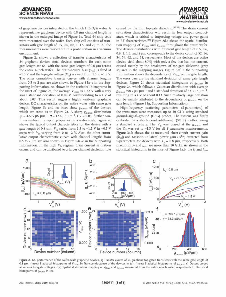
High-frequency scattering parameters (S-parameters) of the transistors were measured up to 30 GHz using standard ground–signal–ground (GSG) probes. The system was firstly calibrated by a short-open-load-through (SOLT) method using a standard substrate. The Vtg was biased at the gm,max and the Vds was set to −1.5 V for all S-parameter measurements. Figure 3a,b shows the as-measured short-circuit current gain (|h21|) and Mason’s unilateral power gain (U1/2) extracted from S-parameters for devices with Lg = 0.8 µm, respectively. Both maximum fT and fmax are more than 10 GHz. As shown in the statistical histograms in the inset of Figure 3a,b, the fT and fmax
Adv. Electron. Mater. 2019, 1800711
Figure 2. DC performance of the wafer-scale graphene devices. a) Transfer curves of 54 graphene top-gated transistors with the same gate length of 0.8 µm. (Inset) Statistical histograms of VDirac. b) Transconductance of the devices in (a). (Inset) Statistical histograms of gm,max. c) Output curves at various top-gate voltages. d,e) Spatial distribution mapping of VDirac and gm,max measured from the entire 4-inch wafer, respectively. f) Statistical histograms of gm,max in (e).
www.advancedsciencenews.com
© 2019 WILEY-VCH Verlag GmbH & Co. KGaA, Weinheim1800711 (4 of 6)
www.advelectronicmat.de
are 8.6 ± 1.3 and 8.3 ± 1.9 GHz, corresponding to the CV of 0.15 and 0.23, respectively. The other cumulative |h21| and U1/2 curves with channel lengths from 0.5 to 2 µm are also shown in Figures S5 and S6 in the Supporting Information, respec-tively. We note that the uniformity for fT is better than that of fmax. Due to the dependence of RF performance on the device gate length, we use the fT*Lg and fmax/fT to characterize the uniformity for different gate length devices. Figure 3c,d shows the spatial distribution mapping of fT*Lg and fmax/fT throughout the entire wafer with different gate lengths, respectively. Figure 3e shows statistical histograms of fmax/fT in Figure 3d. The fT*Lg and fmax/fT are 6.86 ± 2.23 GHz · μm and 0.99 ± 0.11, respectively. The CV for fmax/fT is about 0.11, indicating highly uniform RF characteristics across the whole wafer. The high fmax/fT is mainly due to the drain current saturation in the output characteristics. The relatively large variation of fT*Lg can be mainly attributed to the dependence of fT*Lg on the gate length, as shown in Figure 3f. The as-measured fT*Lg decreases when the gate length decreases, which can be explained by larger parasitic effect of access resistance in short channel graphene transistors.[3] The intrinsic RF metrics are obtained by an intrinsic de-embedding process. The de-embedding structures are shown in Figure S7 in the Supporting Informa-tion. The typical intrinsic |h21| and U1/2 curves with channel lengths from 0.5 to 2 µm are shown in Figures S8 and S9 in the Supporting Information, respectively. Figure 3f shows the as-measured and intrinsic fT*Lg versus Lg. The intrinsic fT*Lg is high up to 20 GHz · μm, which is among the best value for the graphene RF transistors available on wafer-scale device fabrica-tion (Table S1, Supporting Information).
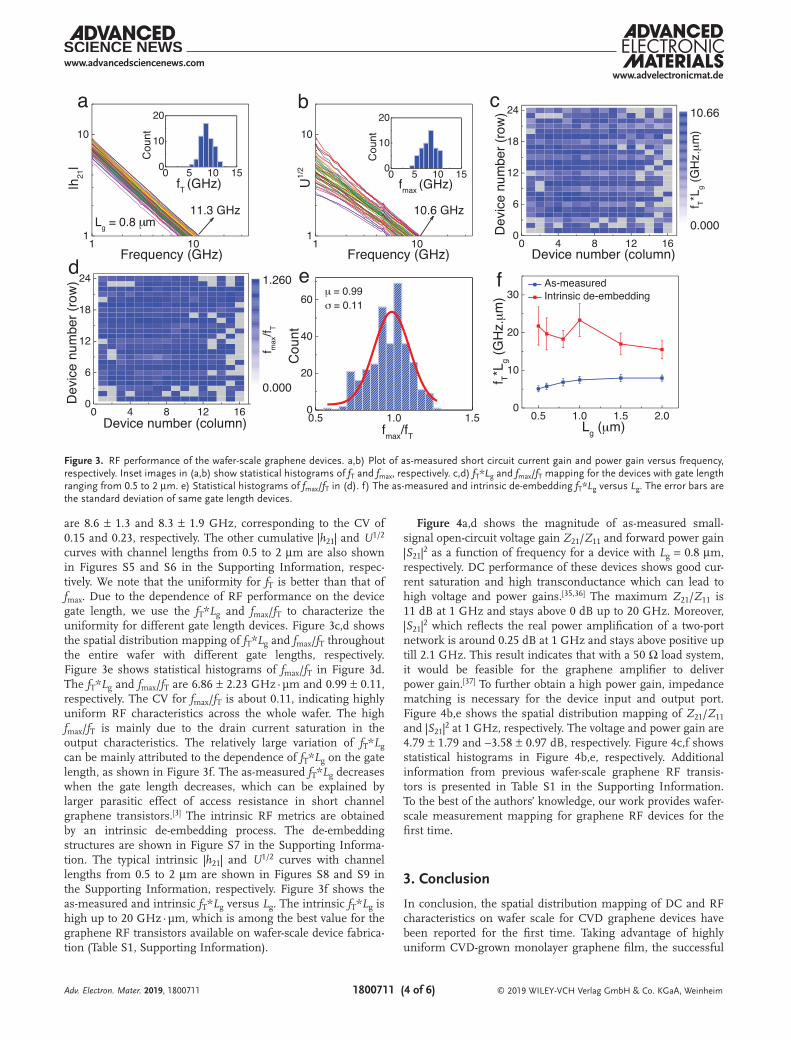
Figure 4a,d shows the magnitude of as-measured small-signal open-circuit voltage gain Z21/Z11 and forward power gain |S21|2 as a function of frequency for a device with Lg = 0.8 µm, respectively. DC performance of these devices shows good cur-rent saturation and high transconductance which can lead to high voltage and power gains.[35,36] The maximum Z21/Z11 is 11 dB at 1 GHz and stays above 0 dB up to 20 GHz. Moreover, |S21|2 which reflects the real power amplification of a two-port network is around 0.25 dB at 1 GHz and stays above positive up till 2.1 GHz. This result indicates that with a 50 Ω load system, it would be feasible for the graphene amplifier to deliver power gain.[37] To further obtain a high power gain, impedance matching is necessary for the device input and output port. Figure 4b,e shows the spatial distribution mapping of Z21/Z11 and |S21|2 at 1 GHz, respectively. The voltage and power gain are 4.79 ± 1.79 and −3.58 ± 0.97 dB, respectively. Figure 4c,f shows statistical histograms in Figure 4b,e, respectively. Additional information from previous wafer-scale graphene RF transis-tors is presented in Table S1 in the Supporting Information. To the best of the authors’ knowledge, our work provides wafer-scale measurement mapping for graphene RF devices for the first time.
3. Conclusion
In conclusion, the spatial distribution mapping of DC and RF characteristics on wafer scale for CVD graphene devices have been reported for the first time. Taking advantage of highly uniform CVD-grown monolayer graphene film, the successful
Adv. Electron. Mater. 2019, 1800711
Figure 3. RF performance of the wafer-scale graphene devices. a,b) Plot of as-measured short circuit current gain and power gain versus frequency, respectively. Inset images in (a,b) show statistical histograms of fT and fmax, respectively. c,d) fT*Lg and fmax/fT mapping for the devices with gate length ranging from 0.5 to 2 µm. e) Statistical histograms of fmax/fT in (d). f) The as-measured and intrinsic de-embedding fT*Lg versus Lg. The error bars are the standard deviation of same gate length devices.

www.advancedsciencenews.com
© 2019 WILEY-VCH Verlag GmbH & Co. KGaA, Weinheim1800711 (5 of 6)
www.advelectronicmat.de
integration of graphene RF devices on a wafer scale has been achieved by not only enhancing the performance of individual graphene device but also uniform performance across total 331 devices. Our work represents an important step toward wafer-scale integration of highly uniform and scalable CVD graphene RF transistors for practical applications.
4. Experimental SectionGraphene Growth and Transfer: Twenty five micrometer thick copper foil
(99.8%, Alfa Aesar 46365) was cleaned in turn by ammonium persulfate solution, deionized water, and isopropanol to remove the surface oxide and organic impurity. The copper foil was made into a large pocket with a size of 12 cm × 6 cm (Figure S1a, Supporting Information) and then loaded into the low-pressure CVD system with a 3-inch quartz tube. Subsequently, the growth system was heated to 1070 °C under an Ar flow of 100 sccm, following the annealing of the copper substrate for 60 min. The mixed gas with CH4 and H2 were then introduced into the system for monolayer graphene growth at flow rates of 0.8 and 60 sccm, respectively. The Ar flow was cutoff in the process of graphene growth. After 8 h, the sample was cooled down to room temperature by dragging the furnace away from the heating zone, while retaining the same H2 and CH4 flow rates. After the growth, the copper pocket with full coverage graphene film in the inner pocket was unfolded into a rectangle piece with a size of about 10 cm × 10 cm. The graphene films were transferred onto the target substrate using a PMMA-assisted transfer method. Only the inner copper surface was spin-coated with a layer of PMMA. Then the PMMA/graphene/Cu stack was floated over the ammonium persulfate solution to etch the copper. After 30 min initial etching stage, the other side of the sample without PMMA coating was washed with deionized water to remove the unwanted graphene. The remaining copper foil was fully
etched away for another 8 h. The resulting graphene/PMMA membranes were thoroughly rinsed with deionized water and then transferred onto the target substrates. Finally, the PMMA was dissolved in acetone, and then rinsed in isopropanol followed by blow-drying with nitrogen gas.
HfSiO Film Growth: High resistive silicon wafer (104 Ω·cm) was cleaned using standard RCA-1 solution and served as the low-loss substrate. Then 20 nm HfSiO film was deposited on the top of the silicon substrate. The deposition was performed at 300 °C using the ALD system (Beneq TFS 200) with Tetrakis[EthylMethylAmino]Hafnium(TEMAH), tris(dimethylamino)silane (TDMAS), and ozone (O3) as precursors for Hf, Si, and O, respectively. The cycle ratios of HfO2 and SiO2 were 16:1 with long purge time. Finally, the film was annealed by rapid thermal annealing at 650 °C for 10 s in a nitrogen ambient to improve the dielectric film quality.
Device Fabrications and Characterization: Reactive ion etching (100 sccm O2, 100 W for 10 s) was used to define the graphene channel and isolate adjacent devices. Subsequently, electron-beam evaporation of 20 nm Pd/60 nm Au followed by a liftoff process was used to define source/drain electrodes. Eighty nanometer Al was then deposited as the top gate metal using the same process as above. Following Al evaporation, the devices were heated on a hot plate at 180 °C for 5 min to form a thin AlOx dielectric layer around the Al wire. Additional annealing process was carried out in a vacuum annealing furnace at 200 °C for 2 h to improve the quality of the AlOx. The DC electrical transport measurements were conducted in a lakeshore probe station using an Agilent parameter analyzer B1500A. The RF measurement was conducted with N5225A network analyzer.
Supporting InformationSupporting Information is available from the Wiley Online Library or from the author.
Adv. Electron. Mater. 2019, 1800711
0.01 0.1 1 10-8
-4
0
|S21
|2 (dB
)
Lg = 0.8 µ m
Frequency (GHz)-15 -10 -5 0
0
40
80
120
|S21
|2 (dB)
Cou
nt
µ = -3.59 dBσ = 0.97 dB
0.01 0.1 1 100
4
8
12
Z21
/Z11
(dB
)
Lg = 0.8 µ m
Frequency (GHz)0 4 8 12 16
0
6
12
18
24
Z21
/Z11
(dB
)
Device number (column)D
evic
e nu
mbe
r (r
ow)
0.000
11.50
-5 0 5 10 150
40
80
-5 0 5 10 15
Cou
nt
µ = 4.79 dBσ = 1.79 dB
Z21
/Z11
(dB)
0 4 8 12 160
6
12
18
24
|S21
|2 (dB
)
Device number (column)
Dev
ice
num
ber
(row
)
-14.50
0.2500
a b c
d e f
Figure 4. Voltage gain and forward power gain. a,d) Plot of as-measured open-circuit voltage gain and forward power gain versus frequency, respectively. b,e) Spatial distribution mapping of Z21/Z11 and |S21|2 throughout the entire array in the 4-inch wafer, respectively. c,f) Statistical histograms of Z21/Z11 and |S21|2, respectively.

www.advancedsciencenews.com
© 2019 WILEY-VCH Verlag GmbH & Co. KGaA, Weinheim1800711 (6 of 6)
www.advelectronicmat.de
AcknowledgementsThis project was supported by the Natural Science Foundation of China (Grant No. 61574066, 61390504, 61390503 and 11574369).
Conflict of InterestThe authors declare no conflict of interest.
KeywordsCVD graphene, radio frequency transistors, wafer-scale uniformity
Received: October 10, 2018Revised: January 29, 2019
Published online:
[1] K. I. Bolotin, K. J. Sikes, Z. Jiang, M. Klima, G. Fudenberg, J. Hone, P. Kim, H. L. Stormer, Solid State Commun. 2008, 146, 351.
[2] R. S. Shishir, D. K. Ferry, J. Phys.: Condens. Matter 2009, 21, 344201.[3] Y. Wu, Y.-m. Lin, A. A. Bol, K. A. Jenkins, F. Xia, D. B. Farmer, Y. Zhu,
P. Avouris, Nature 2011, 472, 74.[4] Y. Wu, K. A. Jenkins, A. Valdes-Garcia, D. B. Farmer, Y. Zhu,
A. A. Bol, C. Dimitrakopoulos, W. Zhu, F. Xia, P. Avouris, Y.-M. Lin, Nano Lett. 2012, 12, 3062.
[5] C. Yu, Z. Z. He, J. Li, X. B. Song, Q. B. Liu, S. J. Cai, Z. H. Feng, Appl. Phys. Lett. 2016, 108, 013102.
[6] Y. Wu, X. Zou, M. Sun, Z. Cao, X. Wang, S. Huo, J. Zhou, Y. Yang, X. Yu, Y. Kong, G. Yu, L. Liao, T. Chen, ACS Appl. Mater. Interfaces 2016, 8, 25645.
[7] S.-J. Han, A. V. Garcia, S. Oida, K. A. Jenkins, W. Haensch, Nat. Commun. 2014, 5, 3086.
[8] H. Lyu, H. Wu, J. Liu, Q. Lu, J. Zhang, X. Wu, J. Li, T. Ma, J. Niu, W. Ren, H. Cheng, Z. Yu, H. Qian, Nano Lett. 2015, 15, 6677.
[9] H. Lyu, Q. Lu, Y. Huang, T. Ma, J. Zhang, X. Wu, Z. Yu, W. Ren, H.-M. Cheng, H. Wu, H. Qian, Sci. Rep. 2016, 5, 17649.
[10] X. Xu, Z. Zhang, J. Dong, D. Yi, J. Niu, M. Wu, L. Lin, R. Yin, M. Li, J. Zhou, S. Wang, J. Sun, X. Duan, P. Gao, Y. Jiang, X. Wu, H. Peng, R. S. Ruoff, Z. Liu, D. Yu, E. Wang, F. Ding, K. Liu, Sci. Bull. 2017, 62, 1074.
[11] I. V. Vlassiouk, Y. Stehle, P. R. Pudasaini, R. R. Unocic, P. D. Rack, A. P. Baddorf, I. N. Ivanov, N. V. Lavrik, F. List, N. Gupta, K. V. Bets, B. I. Yakobson, S. N. Smirnov, Nat. Mater. 2018, 17, 318.
[12] Y.-M. Lin, C. Dimitrakopoulos, K. A. Jenkins, D. B. Farmer, H.-Y. Chiu, A. Grill, P. Avouris, Science 2010, 327, 662.
[13] J. S. Moon, D. Curtis, M. Hu, D. Wong, C. McGuire, P. M. Campbell, G. Jernigan, J. Tedesco, B. VanMil, R. Myers-Ward, C. Eddy, D. K. Gaskill, J. Robinson, M. Fanton, P. Asbeck, presented at The 5th Eur. Microwave Integr. Circuits Conf. Paris, France, September 2010, pp. 254–257.
[14] J. Lee, C. Hyun-Jong, J. Lee, H. Shin, H. Jinseong, Y. Heejun, L. Sung-Hoon, S. Sunae, S. Jaikwang, U. i. Chung, Y. Inkyeong,
K. Kinam, presented at IEEE Int. Electron Devices Meet. San Francisco, CA, USA, December 2010, pp. 23.5.1–23.5.4.
[15] J. A. Robinson, M. Hollander, M. LaBella, K. A. Trumbull, R. Cavalero, D. W. Snyder, Nano Lett. 2011, 11, 3875.
[16] J. S. Moon, D. K. Gaskill, P. Campbell, P. Asbeck, presented at GOMACTech Conf., Baltimore, MD, USA, June 2011, pp. 1–4.
[17] Y.-M. Lin, A. Valdes-Garcia, S.-J. Han, D. B. Farmer, I. Meric, Y. Sun, Y. Wu, C. Dimitrakopoulos, A. Grill, P. Avouris, K. A. Jenkins, Science 2011, 332, 1294.
[18] A. Badmaev, Y. Che, Z. Li, C. Wang, C. Zhou, ACS Nano 2012, 6, 3371.
[19] C.-H. Yeh, Y.-W. Lain, Y.-C. Chiu, C.-H. Liao, D. R. Moyano, S. S. H. Hsu, P.-W. Chiu, ACS Nano 2014, 8, 7663.
[20] H. Lyu, Q. Lu, J. Liu, X. Wu, J. Zhang, J. Li, J. Niu, Z. Yu, H. Wu, H. Qian, Sci. Rep. 2016, 6, 35717.
[21] S. Rahimi, L. Tao, S. F. Chowdhury, S. Park, A. Jouvray, S. Buttress, N. Rupesinghe, K. Teo, D. Akinwande, ACS Nano 2014, 8, 10471.
[22] A. D. Smith, S. Wagner, S. Kataria, B. G. Malm, M. C. Lemme, M. Östling, IEEE Trans. Electron Devices 2017, 64, 3927.
[23] Q. Gao, X. Li, M. Tian, X. Xiong, Z. Zhang, Y. Wu, IEEE Electron Device Lett. 2017, 38, 1168.
[24] T. Li, Z. Zhang, X. Li, M. Huang, S. Li, S. Li, Y. Wu, Appl. Phys. Lett. 2017, 110, 163507.
[25] T. Gao, X. Li, X. Xiong, M. Huang, T. Li, Y. Wu, IEEE Electron Device Lett. 2018, 39, 769.
[26] A. Das, S. Pisana, B. Chakraborty, S. Piscanec, S. K. Saha, U. V. Waghmare, K. S. Novoselov, H. R. Krishnamurthy, A. K. Geim, A. C. Ferrari, A. K. Sood, Nat. Nanotechnol. 2008, 3, 210.
[27] S. Berciaud, S. Ryu, L. E. Brus, T. F. Heinz, Nano Lett. 2009, 9, 346.
[28] A. C. Ferrari, D. M. Basko, Nat. Nanotechnol. 2013, 8, 235.[29] K. K. H. Smithe, S. V. Suryavanshi, M. Muñoz Rojo, A. D. Tedjarati,
E. Pop, ACS Nano 2017, 11, 8456.[30] G. F. Reed, F. Lynn, B. D. Meade, Clin. Diagn. Lab. Immunol. 2002,
9, 1235.[31] M. Tian, X. Li, T. Li, Q. Gao, X. Xiong, Q. Hu, M. Wang, X. Wang,
Y. Wu, ACS Appl. Mater. Interfaces 2018, 10, 20219.[32] E. Guerriero, P. Pedrinazzi, A. Mansouri, O. Habibpour, M. Winters,
N. Rorsman, A. Behnam, E. A. Carrion, A. Pesquera, A. Centeno, A. Zurutuza, E. Pop, H. Zirath, R. Sordan, Sci. Rep. 2017, 7, 2419.
[33] S.-J. Han, D. Reddy, G. D. Carpenter, A. D. Franklin, K. A. Jenkins, ACS Nano 2012, 6, 5220.
[34] L. Tiaoyang, T. Mengchuan, L. Shengman, H. Mingqiang, X. Xiong, H. Qianlan, L. Sichao, L. Xuefei, W. Yanqing, Adv. Electron. Mater. 2018, 4, 1800138.
[35] H. Wang, X. Wang, F. Xia, L. Wang, H. Jiang, Q. Xia, M. L. Chin, M. Dubey, S.-j. Han, Nano Lett. 2014, 14, 6424.
[36] M. A. Andersson, O. Habibpour, J. Vukusic, J. Stake, Electron. Lett. 2012, 48, 861.
[37] Y. Q. Wu, D. B. Farmer, A. Valdes-Garcia, W. J. Zhu, K. A. Jenkins, C. Dimitrakopoulos, P. Avouris, Y. M. Lin, presented at Int. Electron Devices Meet.Washington, DC, USA, October 2011, pp. 23.8.1–23.8.3.
Adv. Electron. Mater. 2019, 1800711