Vol. 4, Issue 5, May 2015 A Novel Control Algorithm for ... · P.G. Scholar, Department Of...
7
ISSN(Online): 2319 - 8753 ISSN (Print) :2347 - 6710 International Journal of Innovative Research in Science, Engineering and Technology (An ISO 3297: 2007 Certified Organization) Vol. 4, Issue 5, May 2015 Copyright to IJIRSET DOI: 10.15680/IJIRSET.2015.0405073 3022 A Novel Control Algorithm for Conversion of AC-DC with Improved Power Factor and Efficiency Ch.Sumalatha 1 , M.Sreenivasulu Reddy 2 P.G. Scholar, Department Of Electrical Engineering, SIETK, Puttur, A.P., India 1 Assistant Professor, Department Of Electrical Engineering, SIETK, Puttur, A.P., India 2 ABSTRACT:A Single power-conversion ac–dc converter with high power factor and high efficiency. The proposed converter is derived by integrating a full-bridge diode rectifier and a series-resonant active-clamp dc–dc converter. To obtain a high power factor without a power factor correction circuit, this paper proposes a novel control algorithm. The proposed converter provides single power-conversion by using the novel control algorithm for both power factor correction and output control. Also, the active-clamp circuit clamps the surge voltage of switches and recycles the energy stored in the leakage inductance of the transformer. Moreover, it provides zero-voltage turn-on switching of the switches. Also, a series-resonant circuit of the output-voltage doubler removes the reverse-recovery problem of the output diodes. The proposed converter provides maximum power factor 0.995 and maximum efficiency of 95.1% at the full load. KEYWORDS:Active-clamp circuit, series-resonant circuit, single power-conversion. I.INTRODUCTION GENERALLY, the ac–dc converter consists of a full-bridge diode rectifier, a dc-link capacitor and a high frequency dc–dc converter. These converters absorb energy from the ac line only when the rectified line voltage is higher than the dc link voltage. Therefore, these kinds of converters have a highly distorted input current, resulting in a large amount of harmonics and a low power factor. To solve the harmonic pollution caused by ac –dc converters, a number of power factor correction (PFC) ac–dc converters have been proposed and developed[1]-[8] . The PFC ac–dc converter can be implemented by using two power-processing stages. The PFC input stage is used to obtain high power factor while maintaining a constant dc-link voltage. Most PFC circuits employ the boost converter . The output stage, which is a high frequency dc–dc converter, gives a desired output. Two power-processing stages require each control circuit consisting of gate drivers and those controllers. In general, the PFC ac –dc converter can be categorized into two types: two-stage ac–dc converters and single stage ac–dc converters. Two-stage ac–dc converters consist of two power- processing stages with their respective control circuits. However, two-stage ac–dc converters raise power losses and the manufacturing cost, eventually reducing the system efficiency and the price competitiveness. In efforts to reduce the component count, the size, and the cost, a number of single-stage ac–dc converters have been proposed and developed. The main idea is that a PFC input stage and a high frequency dc–dc converter are simplified by sharing common switches so that the PFC controller, the PFC switch, and its gate driver can be eliminated. . II.CONVENTIONAL METHOD Fig. 1(a) shows the schematic diagram of the conventional two-stage ac–dc converter. It comprises a full-bridge diode rectifier, a PFC circuit, a control circuit for the PFC circuit, a high frequency dc –dc converter, and a control circuit for output control. The control circuit is composed of gate-drivers and a controller. Namely, two-stage ac–dc converters have two power processing stages with their respective control circuits. Also, the boost type PFC converter used in most PFC input stages requires the dc-link electrolytic capacitor and the inductor. Two control circuits, the dc-link capacitor and the inductor raise the size, weight and the cost of the converter and reduce the price competitiveness. On the other hand, the advantage is to decouple control of the dc-link capacitor voltage from that of the output voltage and
Transcript of Vol. 4, Issue 5, May 2015 A Novel Control Algorithm for ... · P.G. Scholar, Department Of...

ISSN(Online): 2319 - 8753
ISSN (Print) :2347 - 6710
International Journal of Innovative Research in Science,
Engineering and Technology
(An ISO 3297: 2007 Certified Organization)
Vol. 4, Issue 5, May 2015
Copyright to IJIRSET DOI: 10.15680/IJIRSET.2015.0405073 3022
A Novel Control Algorithm for Conversion of
AC-DC with Improved Power Factor and
Efficiency Ch.Sumalatha
1, M.Sreenivasulu Reddy
2
P.G. Scholar, Department Of Electrical Engineering, SIETK, Puttur, A.P., India1
Assistant Professor, Department Of Electrical Engineering, SIETK, Puttur, A.P., India2
ABSTRACT:A Single power-conversion ac–dc converter with high power factor and high efficiency. The proposed
converter is derived by integrating a full-bridge diode rectifier and a series-resonant active-clamp dc–dc converter. To
obtain a high power factor without a power factor correction circuit, this paper proposes a novel control algorithm. The
proposed converter provides single power-conversion by using the novel control algorithm for both power factor
correction and output control. Also, the active-clamp circuit clamps the surge voltage of switches and recycles the
energy stored in the leakage inductance of the transformer. Moreover, it provides zero-voltage turn-on switching of the
switches. Also, a series-resonant circuit of the output-voltage doubler removes the reverse-recovery problem of the
output diodes. The proposed converter provides maximum power factor 0.995 and maximum efficiency of 95.1% at the
full load.
KEYWORDS:Active-clamp circuit, series-resonant circuit, single power-conversion.
I.INTRODUCTION
GENERALLY, the ac–dc converter consists of a full-bridge diode rectifier, a dc-link capacitor and a high
frequency dc–dc converter. These converters absorb energy from the ac line only when the rectified line voltage is
higher than the dc link voltage. Therefore, these kinds of converters have a highly distorted input current, resulting in a
large amount of harmonics and a low power factor. To solve the harmonic pollution caused by ac–dc converters, a
number of power factor correction (PFC) ac–dc converters have been proposed and developed[1]-[8] . The PFC ac–dc
converter can be implemented by using two power-processing stages. The PFC input stage is used to obtain high power
factor while maintaining a constant dc-link voltage. Most PFC circuits employ the boost converter . The output stage,
which is a high frequency dc–dc converter, gives a desired output. Two power-processing stages require each control
circuit consisting of gate drivers and those controllers. In general, the PFC ac–dc converter can be categorized into two
types: two-stage ac–dc converters and single stage ac–dc converters. Two-stage ac–dc converters consist of two power-
processing stages with their respective control circuits. However, two-stage ac–dc converters raise power losses and the
manufacturing cost, eventually reducing the system efficiency and the price competitiveness. In efforts to reduce the
component count, the size, and the cost, a number of single-stage ac–dc converters have been proposed and developed.
The main idea is that a PFC input stage and a high frequency dc–dc converter are simplified by sharing common
switches so that the PFC controller, the PFC switch, and its gate driver can be eliminated. .
II.CONVENTIONAL METHOD
Fig. 1(a) shows the schematic diagram of the conventional two-stage ac–dc converter. It comprises a full-bridge diode
rectifier, a PFC circuit, a control circuit for the PFC circuit, a high frequency dc–dc converter, and a control circuit for
output control. The control circuit is composed of gate-drivers and a controller. Namely, two-stage ac–dc converters
have two power processing stages with their respective control circuits. Also, the boost type PFC converter used in
most PFC input stages requires the dc-link electrolytic capacitor and the inductor. Two control circuits, the dc-link
capacitor and the inductor raise the size, weight and the cost of the converter and reduce the price competitiveness. On
the other hand, the advantage is to decouple control of the dc-link capacitor voltage from that of the output voltage and
ISSN(Online): 2319 - 8753
ISSN (Print) :2347 - 6710
International Journal of Innovative Research in Science,
Engineering and Technology
(An ISO 3297: 2007 Certified Organization)
Vol. 4, Issue 5, May 2015
Copyright to IJIRSET DOI: 10.15680/IJIRSET.2015.0405073 3023
realize much tighter output control.However, the single stage ac-dc converters have several disadvantages.First, the
power factor is also related to the controller, indicating that the variation of the load or the input voltage will change
the power factor. Second, the output voltage control bandwidth is limited to a few hertz not to excessively distort the
input current. Third, single-stage ac–dc converters require the dc-link electrolytic capacitor and the inductor for the
PFC circuit, just like two-stage converters. Finally, the conventional single-stage ac–dc converters have highvoltage
stresses or low power factor.
Fig. 1. Block diagrams of the conventional PFC converter (a) Two-stage converter. (b) Single-stage converter.
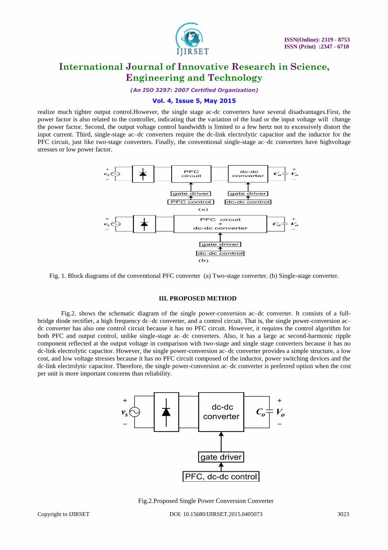
III. PROPOSED METHOD
Fig.2. shows the schematic diagram of the single power-conversion ac–dc converter. It consists of a full-
bridge diode rectifier, a high frequency dc–dc converter, and a control circuit. That is, the single power-conversion ac–
dc converter has also one control circuit because it has no PFC circuit. However, it requires the control algorithm for
both PFC and output control, unlike single-stage ac–dc converters. Also, it has a large ac second-harmonic ripple
component reflected at the output voltage in comparison with two-stage and single stage converters because it has no
dc-link electrolytic capacitor. However, the single power-conversion ac–dc converter provides a simple structure, a low
cost, and low voltage stresses because it has no PFC circuit composed of the inductor, power switching devices and the
dc-link electrolytic capacitor. Therefore, the single power-conversion ac–dc converter is preferred option when the cost
per unit is more important concerns than reliability.
Fig.2.Proposed Single Power Conversion Converter

ISSN(Online): 2319 - 8753
ISSN (Print) :2347 - 6710
International Journal of Innovative Research in Science,
Engineering and Technology
(An ISO 3297: 2007 Certified Organization)
Vol. 4, Issue 5, May 2015
Copyright to IJIRSET DOI: 10.15680/IJIRSET.2015.0405073 3024
Fig. 3. Proposed single power-conversion ac–dc converter and the control block diagram.
The operating modes of the input side and the output side are shown in Figs. 4 and 5, respectively. The
rectified input voltage
Vi is |vin | = |Vmsinωt|………………………….1
where Vm is the amplitude of the input voltage and ω is the angular frequency of the input voltage. Priorto Mode 1, the
primary current i1 is a negative direction and the secondary current i2 is zero.
Mode 1 [t0, t1 ]:At the time t0 , the voltage vs1 across S1 becomes zero and Ds1 begins to conduct power. After the
timet0, S1 is turned on. Since i1 started flowing through Ds1 before S1 was turned on, S1 achieves the ZVS turn-on. As
shown in fig.4
io (t) = i2 (t) − ic1 (t) =1/2iD1 (t)……………….2
Mode 2 [t1, t2 ]:At the time t1, i1 changes its direction to positive. Llk and Cr still resonate similar to Mode1.
Mode 3 [t2, t3 ]:At the time t2, i2 becomes zero and D1 is maintained in the on-state with the zero current. I1 and im
are equal during this interval. Therefore, i1 terminates the first resonance and increases linearly as (1).
Mode 4 [t3, t4 ]:At the time t3, S1 is turned off and D1 is turned off with the zero current. The ZCS turn-off of D1-
removes its reverse-recovery problem. The voltage vs2 across S2 becomes zero and the body diode Ds2 begins to
conduct power. After the time t3 , the ZVS turn-on of the auxiliary switch S2 is achieved.
Mode 5 [t4, t5 ]:At the time t4, Llk and Cr still resonate similar to Mode 4. In addition, i1 may change its
directionduring this interval based on the designed resonant frequencyAt the time t4, Llk and Cr still resonate similar to
Mode 4. In addition, i1 may change its direction during this interval based on the designed resonant frequency f.
Mode 6 [t5, t6 ]:At the time t5, i2 becomes zero and D2 is maintained to the on-state with the zero current. i1 and imare
equal during this mode. Therefore, i1 terminates the series resonance and decreases linearly as (9). At the end of this
mode,D2 is turned off with the zero current. The ZCS turn-off of D2 removes its reverse-recovery problem.

ISSN(Online): 2319 - 8753
ISSN (Print) :2347 - 6710
International Journal of Innovative Research in Science,
Engineering and Technology
(An ISO 3297: 2007 Certified Organization)
Vol. 4, Issue 5, May 2015
Copyright to IJIRSET DOI: 10.15680/IJIRSET.2015.0405073 3025
Fig4: Operating modes of the proposed ac–dc converter.
Fig. 5. Theoretical waveforms of the proposed converter. (a) Input side waveforms. (b) Output side waveforms.

ISSN(Online): 2319 - 8753
ISSN (Print) :2347 - 6710
International Journal of Innovative Research in Science,
Engineering and Technology
(An ISO 3297: 2007 Certified Organization)
Vol. 4, Issue 5, May 2015
Copyright to IJIRSET DOI: 10.15680/IJIRSET.2015.0405073 3026
IV. CONTROL ALGORITHM
The proposed converter has no PFC circuit. Therefore, to obtain a high power factor, it requires the control
algorithm for both PFC and output control. The duty ratio D according to the input current iin is hard to control because
the relation of D and iin is nonlinear. To achieve good controllability, the nonlinear system needs to be transformed
into the linear system by the feedback linearization.
FIG6: CONTROL BLOCK DIAGRAM OF THE PROPOSED CONVERTER
Fig. 6 shows the control block diagram of the proposed converter. The voltage controller attempts to minimize the error
value as the difference between Vo ,ref and the measured output voltage by adjusting 𝑖˳ ∗that is, i˳*is calculated by the
voltage controller, and then is calculated by the PFC rule in Fig. 6. In order to realize the PFC rule,
synchronization with input voltage vin is necessary. Since Vi includes the information about the amplitude and the
phase of vin , the synchronization with vin is implemented by using Vi as shown in Fig. 2.
The current controller attempts to , i˳*minimize the error value as the difference betweenand the measured
output current io by adjustingΔD. Finally, D is obtained by adding ΔD to Dn . The proposed control system consists of
the inner loop and the outer loop. The inner loop is the current control loop and the outer loop is the output voltage
control loop. The proposed control system is analyzed by using a small signal model. The crossover frequency of the
open-loop transfer function Tv (s) for the voltage controller is chosen much smaller than the open-loop transfer function
Ti(s) for the inner current loop. The open-loop transfer functions Ti(s) and Tv (s) are expressed as
Ti(s) = Hi · Cic (s) · Gid (s) ……………………..3
Tv (s) = Hv · Cvc (s) · Gvi(s)………………………4
where Hi(s) and Hv (s) are current sensor gain and voltage sensor gain, respectively. The small signal transfer functions
of the duty ratio-to-output current and the output current-to voltage, respectively, can be obtained as follows
I˳*=I˳*(VI/VM)2..........................................................5
V. SIMULATION AND RESULTS
A simulation design of minimization method for single phase inverter without an output filter is implemented in
MATLAB/ SIMULINK with the help of wing energy, boost rectifier, universal bridge, controllers and FFT as shown in
figure 8

ISSN(Online): 2319 - 8753
ISSN (Print) :2347 - 6710
International Journal of Innovative Research in Science,
Engineering and Technology
(An ISO 3297: 2007 Certified Organization)
Vol. 4, Issue 5, May 2015
Copyright to IJIRSET DOI: 10.15680/IJIRSET.2015.0405073 3027
.
Fig. 8 Simulation model
The output waveform of inverter output as shown in figure 10a.When manual switch is connect directly to the output of
inverter, there is a dc voltage of 1 V appears at output. After switch connected to PI, the output voltage is minimized as
shown in figure 10b.
Fig9(a)
Fig9(b)
Fig. 9 Output voltage of inverter: a) Inverter output voltage, b) dc at output voltage
The THD value can be obtained by using FFT analysis, as shown in figure 11 and frequency spectrum of proposed
system as shown in figure 12. Both are clearly shows harmonics are minimized and THD obtained is 4.24% , complies
with the limit imposed by the standards.
Before switch connected to
PI controller With PI controller

ISSN(Online): 2319 - 8753
ISSN (Print) :2347 - 6710
International Journal of Innovative Research in Science,
Engineering and Technology
(An ISO 3297: 2007 Certified Organization)
Vol. 4, Issue 5, May 2015
Copyright to IJIRSET DOI: 10.15680/IJIRSET.2015.0405073 3028
Fig. 10. FFT analysis
Fig 11:Frequency spectrum
VI.CONCLUSION
A novel approach to harmonic minimization method for single phase inverter established on mirror injection of
harmonic and elimination of dc principle has been proposed. The following conclusions can be drawn after the
imaginary analysis and the experimental results reported in this paper the proposed system minimizes the harmonics
generated by the switching operation as well as harmonics generated by dc nature of the source and external point i.e.
grid. Improvement of THD, through the cancellation of low-order harmonics and minimization of dc , so that the output
voltage complies with the limit imposed by the standards, without the use of a filter.
REFERENCES
[1] Yong-Won Cho, Jung-Min Kwon, and Bong-Hwan Kwon,” Single Power-Conversion AC–DC Converter With High Power Factor and High
Efficiency”, ieee transactions on power electronics, vol. 29, no. 9, PP.4797 4806,september 2014.
[2] B. Singh, B. N. Singh, A. Chandra, K. Al-Haddad, A. Pandey, and D. P. Kothari, “A review of single-phase improved power quality AC– DC converters,” IEEE Trans. Ind. Electron., vol. 50, no. 5, pp. 962–981, Oct. 2003.
[3] B. Singh, B. N. Singh, A. Chandra, K. Al-Haddad, A. Pandey, andD. P. Kothari, “A review of three-phase improved power quality ac–
dcconverters,” IEEE Trans. Ind. Electron., vol. 51, no. 3, pp. 641–660, Jun.2004. [4] H. S. Kim, M. H. Ryu, J. W. Baek, and J. H. Jung, “High-efficiency isolatedbidirectional AC–DC converter for a DC distribution system,”
IEEETrans. Power Electron., vol. 28, no. 4, pp. 1642–1654, Apr. 2013.
[5] M. Arias, D. G. Lamar, J. Sebastian, D. Balocco, and A. A. Diallo, “HighefficiencyLED driver without electrolytic capacitor for street lighting,”IEEE Trans. Ind. Appl., vol. 49, no. 1, pp. 127–137, Jan./Feb. 2013.
[6] B. Tamyurek and D. A. Torrey, “A three-phase unity power factor singlestageAC–DC converter Based on an interleaved flyback topology,”
IEEETrans. Power Electron., vol. 26, no. 1, pp. 308–318, Jan. 2011. [7] S. C.Moon, G. B. Koo, and G. W.Moon, “A new control method of interleavedsingle-stage flyback AC–DC converter for outdoor LED
lightingsystems,” IEEE Trans. Power Electron., vol. 28, no. 8, pp. 4051–4062, Aug. 2013.
[8] M. Narimani and G. Moschopoulos, “A new single-phase single-stagethree-level power factor correctionAC–DCconverter,” IEEE Trans. PowerElectron., vol. 27, no. 6, pp. 2888–2899, Jun. 2012.
[9] C. Y. Oh, D. H. Kim, D. G. Woo, W. Y. Sung, Y. S. Kim, and B. K. Lee,“A high-efficient nonisolated single-stage on-board battery charger
forelectric vehicles,” IEEE Trans. Power Electron., vol. 28, no. 12, pp. 5746–5757, Dec. 2013.


![vlsi & embedded systems lab - SIETK ECE DEPARTMENT · 2018. 7. 16. · SIETK, ECE [VLSI & EMBEDDED SYSTEMS LAB] 2 (15A04712) VLSI & EMBEDDED SYSTEMS LABORATORY Note: The students](https://static.fdocuments.us/doc/165x107/60a68df82b16b22c09239fcb/vlsi-embedded-systems-lab-sietk-ece-department-2018-7-16-sietk-ece.jpg)