VLSI Design EE213 VLSI DesignStephen Daniels 2003 VLSI Design EE213 Dr. Stephen Daniels.
Upload
ali-siddiquiCategory
view
23download
7description
Co
VL
CoS
ompu
SI De
ompuSir Syed
uter
esignFa
ter Ed Univer
Un
Lab
n Tecall Sem
Enginersity of Eniversity R
http://w
borat
chniqmester 2
eeringEngineeRoad, Kar
www.ssuet
tory
ques 2012
g Depring & Trachi 7530t.edu.pk
Man
(CE-
partmTechnolo00
nual
-410)
ment ogy
)

TABLE OF CONTENTS
Lab No. TITLE PAGE No
1. Introduction to Xilinx ISE 13.4 + Basic Schematic Example and Simulation 1 - 32
2. Combinational Logic Schematic Example and Simulation. 33 - 39
3. Sequential Logic Schematic Example and Simulation. 40 - 50
4. Introduction to Verilog Language, Gate Level Modeling and Example. 51 - 59
5. Define expressions, operators, and operands. Use dataflow constructs to model practical digital circuits in Verilog 60 - 67
6. Introduction to behavioral modeling 68 - 77
7. Hierarchal model 78 - 86
8. Midterm 8th week
9. To study the characteristics of logic gates delays and to calculate and measure the output of logic gates delays 87 - 93
10. State Machines 94 - 111
11. Introduction to Virtex 5 Development System 112 - 149
12. Lab Quiz
13. Projects related to Virtex-5 Development System
14. Projects related to Virtex-5 Development System
15. Lab Viva
16. Lab Viva

Lab 1
VLSI LAB Page 1
LAB 1 OBJECTIVE: This lab is designed to help you to become familiar with the operation of the WebPack software by creating a simple Schematic design (half adder /full adder) and simulating it on the Xilinx ISim simulator. INTRODUCTION TO XILINX ISE WEB PACK SOFTWARE:
Introduction to Xilinx ISE Environment:
Design Flow
The typical design flow for designing the VLSI circuits is shown. This design flow is typically used by the designers who use HDLs.

Lab 1
VLSI LAB Page 2
Integrated Software Environment (ISE)
Xilinx Integrated Software Environment (ISE) is a powerful yet flexible integrated design environment. It allows designing of Xilinx FPGA devices from start to finish. ISE enables us to start our design with any of a number of different source types i.e. Verilog HDL, VHDL, Schematic Design etc.
Design Flow in ISE
There are different ways to define our design in ISE. ISE Text Editor, Schematic Editor, Core Generator, Constrains Editor, Pinout area Constraint Editor, State CAD editor, Test Bench Waveform.
Lab 1
VLSI LAB Page 3
Design Flow in ISE (Implementation)
Translate - The Translate process merge all of the input netlists as well as design constraint information into a Xilinx database file. Map - The Map program maps a logical design to a Xilinx FPGA. Place and Route (PAR) - The PAR program accepts the mapped design, places and routes the FPGA, and produces output for the bit stream generator. Floor Planner - The Floor Planner allows you to view a graphical representation of the FPGA, and to view and modify the placed design. FPGA Editor - The FPGA Editor allows you view and modify the physical implementation, including routing.
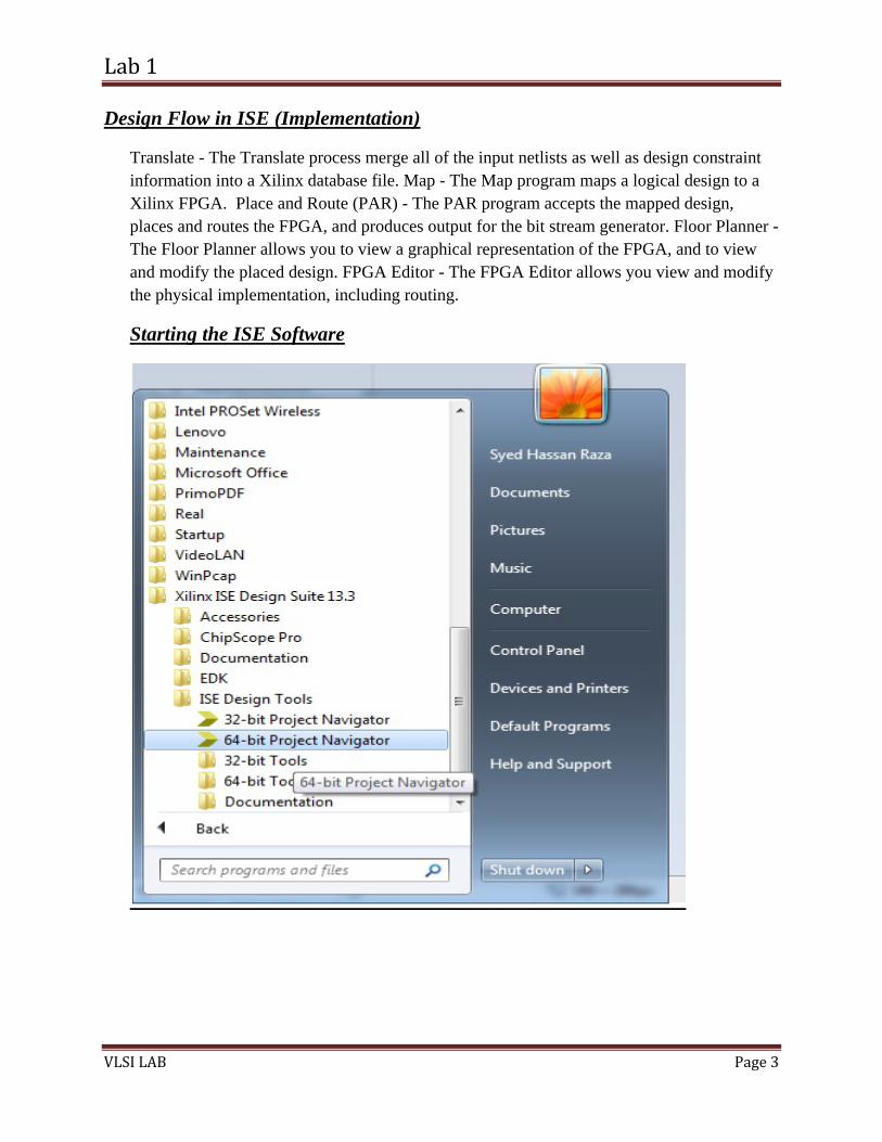
Starting the ISE Software

Lab 1
VLSI LAB Page 4
Create New Project

Lab 1
VLSI LAB Page 5
Project Name & Working Directory

Lab 1
VLSI LAB Page 6
select spartan 3e starter board

Lab 1
VLSI LAB Page 7
show the project summary

Lab 1
VLSI LAB Page 8
Design and process directory
Lab 1
VLSI LAB Page 9
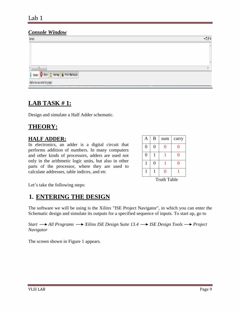
Console Window
LAB TASK # 1: Design and simulate a Half Adder schematic. THEORY: HALF ADDER: In electronics, an adder is a digital circuit that performs addition of numbers. In many computers and other kinds of processors, adders are used not only in the arithmetic logic units, but also in other parts of the processor, where they are used to calculate addresses, table indices, and etc
A B sum carry
0 0 0 0
0 1 1 0
1 0 1 0
1 1 0 1
Truth Table Let’s take the following steps: 1. ENTERING THE DESIGN
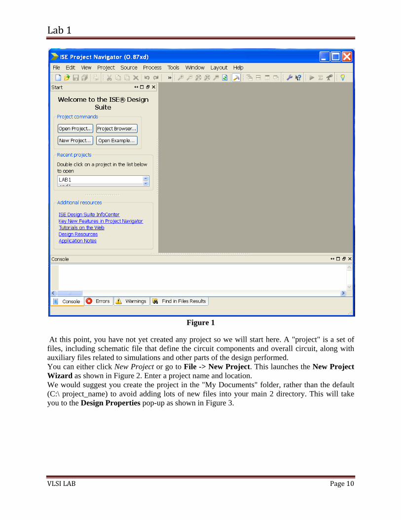
The software we will be using is the Xilinx "ISE Project Navigator", in which you can enter the Schematic design and simulate its outputs for a specified sequence of inputs. To start up, go to Start All Programs Xilinx ISE Design Suite 13.4 ISE Design Tools Project Navigator
The screen shown in Figure 1 appears.
Lab 1
VLSI LAB Page 10
Figure 1
At this point, you have not yet created any project so we will start here. A "project" is a set of files, including schematic file that define the circuit components and overall circuit, along with auxiliary files related to simulations and other parts of the design performed. You can either click New Project or go to File -> New Project. This launches the New Project Wizard as shown in Figure 2. Enter a project name and location. We would suggest you create the project in the "My Documents" folder, rather than the default (C:\ project_name) to avoid adding lots of new files into your main 2 directory. This will take you to the Design Properties pop-up as shown in Figure 3.

Lab 1
VLSI LAB Page 11
Figure 2

Lab 1
VLSI LAB Page 12
Figure 3
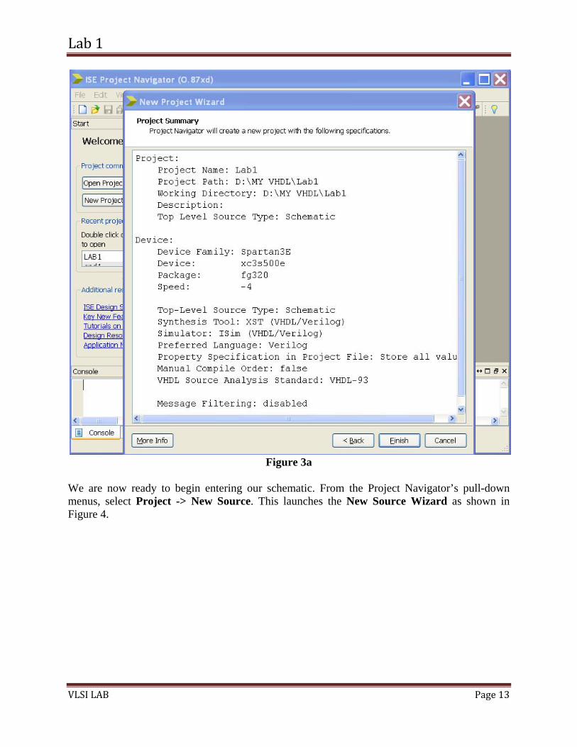
In the Design Properties window, you can specify the Device Family and the Device. This is needed when you reach the "synthesis" stage in the design and implementation since the synthesis stage needs to know the internal design of the specific programmable device. When you click OK, a Project Summary window will pop-up. Click Finish (figure 3a).
Lab 1
VLSI LAB Page 13
Figure 3a
We are now ready to begin entering our schematic. From the Project Navigator’s pull-down menus, select Project -> New Source. This launches the New Source Wizard as shown in Figure 4.

Lab 1
VLSI LAB Page 14
Figure 4
This window can be used to add a variety of sources to your design. Select "Schematic" and add the name of your circuit. The box "Add to project" should be checked. The location should appear as the directory you selected above. Click Next and the screen shown in Figure 5 appears.

Lab 1
VLSI LAB Page 15
Figure 5

Lab 1
VLSI LAB Page 16
Figure 6
The screen in Figure 6 allows you to enter the "Schematic" of half adder. Design the schematics by drag drop the symbols of logic gates involve in schematic as shown in Figure 7.

Lab 1
VLSI LAB Page 17
Figure 7
Save the file. Click on Design option at the bottom of the process window select your file and expand the Design Utilities option. Click on Check Design Rules, if it will be correct a green arrow will appear. Then click Create Schematic Symbol to make your schematic a symbol for further use. Again a green arrow will appear. All this is shown in the left of figure 7. 2. SIMULATING THE CIRCUIT Now that we have a design that has been checked for its syntax, we can now proceed to a simulation of the circuit designed. In order to simulate the circuit, we first need a set of signals to drive our inputs A and B. We do this by constructing a separate source file called a test fixture. This code defines the signals and then applies them to the entity under test.

Lab 1
VLSI LAB Page 18
Figure 8
First check the simulation tab in Design panel after that click from the Project Navigator window Project -> New Source. The same New Source Wizard (Figure 8) appears that was used earlier to enter our halfadder schematic. This time, instead of selecting Schematic, select Verilog Test Fixture. Name the file halfadder_tf (to distinguish it from the actual halfadder.sch file) and click Next. New windows will pop-up asking you which module describes the circuit you want to test. There is only one choice – halfadder as shown in figure 9. Select this module and then click Next. The New Source Wizard now shows a summary page. Click Finish.

Lab 1
VLSI LAB Page 19
Figure 9
Clicking on Finish, the Project Navigator screen reappears and you will see that the wizard has already generated some Verilog code, for a new module called halfadder_tf as shown in Figure 10. There may be some compiler errors that appear in the console window. Ignore them because we are going to edit this test fixture file. It is not necessary for you to understand the semantics of this test fixture module at this stage. Simply make the following changes.

Lab 1
VLSI LAB Page 20
module halfadder_tf; // Inputs reg A; reg B; // Outputs wire Sum; wire Carry; // Instantiate the Unit Under Test (UUT) halfadder uut ( .A(A), .B(B), .Sum(Sum), .Carry(Carry) ); initial begin // Initialize Inputs A = 0; B = 0; // Wait 100 ns for global reset to finish #100; // Add stimulus here #100 A = 0; B = 1; #100 A = 0; B = 0; #100 A = 1; B = 1; #100 A = 1; B = 0; end endmodule

Lab 1
VLSI LAB Page 21
Figure 10
Save the file. Select halfadder_tf in the Hierarchy window and then in process panel double click on Behavioral Check Syntax to check for errors. Correct any error if there is, and then save it and check again. Once, the errors are removed, right-click on Simulate Behavioral Model in process panel and select Process Properties. This will generate the Isim Properties pop-up window as shown in Figure 11. Set the Simulation Run Time to 200 ns and click OK.

Lab 1
VLSI LAB Page 22
Figure 11
We are now ready to run the simulation. Double-click on Simulate Behavioral Model. This brings up the ISim simulation window as shown in Figure 12. Waveforms are plotted in the top right-hand window. Note that the simulator very conveniently plots the last 3ps of the simulation! In order to see the whole simulation, click the Zoom to Full View icon in the tool-bar immediately above the simulation window. The waveforms will now appear as shown in Figure 13. Check for correct functionality of the half adder. Note the timing delays as outputs respond to inputs according to the delays we specified in the Verilog test fixture code.

Lab 1
VLSI LAB Page 23
Figure 12

Lab 1
VLSI LAB Page 24
Figure 13

Lab 1
VLSI LAB Page 25
LAB TASK # 2: Design and simulate a full adder using two half adders. THEORY: FULL ADDER: A full adder adds binary numbers and accounts for values carried in as well as out. A one-bit full adder adds three one-bit numbers, often written as A, B, and Ci; A and B are the operands, and Ci is a bit carried in. The circuit produces a two-bit output, S and Co; the final sum is 2 X Co +S.
A B Ci sum Co
0 0 0 0 0
0 0 1 1 0
0 1 0 1 0
0 1 1 0 1
1 0 0 1 0
1 0 1 0 1
1 1 0 0 1
1 1 1 1 1 Truth Table Let’s take the following steps: 1. ENTERING THE DESIGN
Follow the lab task 1 of half adder, start from the new source. From the Project Navigator’s pull-down menus, select Project -> New Source. This launches the New Source Wizard. This window can be used to add a variety of sources to your design. Select "Schematic" and add the name of your circuit. The box "Add to project" should be checked. The location should appear as the directory you selected above. Click Next shown in figure 14.

Lab 1
VLSI LAB Page 26
Figure 14
Design the schematics by drag drop the symbols. Remember you create a symbol of your half adder schematic, now use that symbol to make full adder schematic as shown in Figure 15.

Lab 1
VLSI LAB Page 27
Figure 15
Save the file. Click on Design option at the bottom of the process window select your file and expand the Design Utilities option. Click on Check Design Rules, if it will be correct a green arrow will appear. Then click Create Schematic Symbol to make your schematic a symbol for further use. Again a green arrow will appear. 2. SIMULATING THE CIRCUIT First check the simulation tab in Design panel after that click from the Project Navigator window Project -> New Source. The same New Source Wizard appears that was used earlier to enter our fullfadder schematic. This time, instead of selecting Schematic, select Verilog Test Fixture. Name the file fulladder_tf (to distinguish it from the actual fulladder.sch file) and click Next. A new window will pop-up asking you which module describes the circuit you want to test. Here you have to choice – fulladder module. Select this module and then click Next. The New

Lab 1
VLSI LAB Page 28
Source Wizard now shows a summary page. Click Finish. Clicking on Finish, the Project Navigator screen reappears and you will see that the wizard has already generated some Verilog code. Now for full adder test fixture write the following code: Test Fixture Code: module FullAdder_tf; // Inputs reg A; reg B; reg Cin; // Outputs wire Sum; wire Cout; integer i; // Instantiate the Unit Under Test (UUT) FullAdder uut ( .A(A), .B(B), .Cin(Cin), .Sum(Sum), .Cout(Cout) ); initial begin // Initialize Inputs A = 0; B = 0; Cin = 0; end always @ ( A, B, Cin ) begin // generate truth table for ( i = 0; i < 8; i = i + 1 ) // every 10 ns set a, b, and c to the binary rep. of i #10 {A, B, Cin} = i; // stop 10ns after last change of inputs #10 $stop;

Lab 1
VLSI LAB Page 29
// Wait 100 ns for global reset to finish #100; end endmodule Save the file. Select fulladder_tf in the Hierarchy window and then in process panel double click on Behavioral Check Syntax to check for errors. Correct any errors if there is then save it and check again. Once, the code is free from error, right-click on Simulate Behavioral Model in process panel and select Process Properties. This will generate the Isim Properties pop-up window. Set the Simulation Run Time to 200 ns and click OK. Double-click on Simulate Behavioral Model in process panel. The waveforms will now appear as shown in Figure 16. Check for correct functionality of the full adder. Note the timing delays as outputs respond to inputs according to the delays we specified in the VHDL code.
Your second task is completed successfully. Now add and explain the screen shot of your task#2 design simulation.

Lab 1
VLSI LAB Page 30
LAB TASK # 3: Design and simulate a 4 bit ripple carry Adder using 4 full adders. THEORY: 4 BIT RIPPLE CARRY ADDER:
Multiple Basic (1-bit) Full Adders can be cascaded to form a Multi-bit Full Adder. Four Basic Full Adders are chained together to form a 4-bit Ripple Adder, with the Carry Out (CO) of a Basic Full Adder connected to the Carry In (Cin) of the next most significant Basic Full Adder.
Addition between two Multi-bit Binary Numbers A and B is done by adding the bits successively, starting from the Least Significant Bit (LSB), i.e. A0 + B0. Any Carry bit from previous bits is added to the sum of the next consecutive bits. Let’s take the following steps: 1. ENTERING THE DESIGN
Follow the lab task 2 of full adder, start from the new source. From the Project Navigator’s pull-down menus and select Project -> New Source. This launches the New Source Wizard. This window can be used to add a variety of sources to your design. Select "Schematic" and add the name of your circuit. The box "Add to project" should be checked. The location should appear as the directory you selected above. Click Next. Design the schematics by drag drop the symbols. Remember you create a symbol of your full adder schematic, now use that symbol to make 4 bit ripple carry adder schematic as shown in Figure 17.

Lab 1
VLSI LAB Page 31
Figure 16
Save the file. Click on Design option at the bottom of the process window select your file and expand the Design Utilities option. Click on Check Design Rules, if it will be correct a green arrow will appear. 2. SIMULATING THE CIRCUIT
Again follow the same steps as in example 1 and 2 for creating a test bench file. Write the following code in the test fixture file:

Lab 1
VLSI LAB Page 32
Test Fixture Code: always @ ( A0, A1, A2, A3, B0, B1, B2, B3) begin // generate truth table for ( i = 0; i < 255; i = i + 1 ) // every 10 ns set a, b, and c to the binary rep. of i #10 {A0, A1, A2, A3, B0, B1, B2, B3} = i; // stop 10ns after last change of inputs #10 $stop; // Wait 100 ns for global reset to finish #100;
end
Your third task is completed successfully. Now add and explain the screen shot of your task#3 design simulation.

Lab 2
VLSI LAB Page 33
LAB 2 OBJECTIVE: Combinational Logic Schematic Example and Simulation. LAB TASK # 1: Design and simulate a 4 to 1 Multiplexer. THEORY: 4 TO 1 MULTIPLXER: A multiplexer performs the function of selecting the input on any one of 'n' input lines and feeding this input to one output line. Multiplexers are used as one method of reducing the number of integrated circuit packages required by a particular circuit design. This in turn reduces the cost of the system. A 4x1 multiplexer is shown in figure below, having 4 inputs A, B, C and D and two selection lines S0 and S1. There is a single output Y. The working results are shown in truth table.
4x1 Multiplexer Truth Table

Lab 2
VLSI LAB Page 34
Let’s take the following steps: ENTERING THE DESIGN
Up till now you are familiar with the software Xilinx, you understand how to make a new project and start with new source. So keeping that steps in mind, start from creating the desire schematic. As shown in figure 1 below.
Figure 1
Save the file. Click on Design option at the bottom of the process window select your file and expand the Design Utilities option. Click on Check Design Rules, if it will be correct a green arrow will be appearing. Then click Create Schematic Symbol to make your schematic a symbol for further use. Again a green arrow will appear. SIMULATING THE CIRCUIT Follow the same steps for simulation as in lab 1.

Lab 2
VLSI LAB Page 35
Now for 4x1 multiplexer test fixture write the following code: module multiplexer_multiplexer_sch_tb();
// Inputs reg A; reg B; reg C; reg D; reg s0; reg s1; // Output wire Y; multiplexer UUT ( .A(A), .B(B), .C(C), .D(D), .s0(s0), .s1(s1), .Y(Y) ); initial begin A = 1; B = 0; C = 0; D = 0; s0 = 0; s1 = 0; #100 s0=0;s1=1; #100 s0=1;s1=0; #100 s0=1;s1=1;

Lab 2
VLSI LAB Page 36
end endmodule
Your task is completed successfully. Now add and explain the screen shot of your task design simulation.

Lab 2
VLSI LAB Page 37
LAB ASSIGNMENTS Lab Assignment 1: Design a 3x8 decoder. The theory given below will help you to design the schematic. Also verify the results from truth table given below. 3x8 DECODER:
A decoder is used to determine the ordinal value of a particular bit pattern. In other words, it decodes the number represented by a stream of binary digits. The 3-to-8 line decoder is so named because it takes three input signals and converts them into the correct output signal, choosing from the eight possible values. If the decoder is fed 101 (the binary for 5), the decoder performs the following tasks: x is on, so all AND gates with the negation of x cannot turn on. This leaves gates D1, D3, D5, and D7 as possible output gates. y is off, so all gates without the negation of y cannot turn on. (This turns off D3 and D7.) z is on, and the only gate that could be turned on is therefore D5 (since D1 could only be activated if z were off). The output can be determined by the following Boolean equations: _ _ _ D0 = z y x _ _ D1 = z y x _ _ D2 = z y x _ D3 = z y x _ _ D4 = z y x _ D5 = z y x _ D6 = z y x D7 = z y x

Lab 2
VLSI LAB Page 38
OBSERVATION & RESULT: ________________________________________________________________
________________________________________________________________
________________________________________________________________
________________________________________________________________
_______________________________________________________________

Lab 2
VLSI LAB Page 39
Lab Assignment 2: Design a 8x3 Encoder / Multiplexer. Theory given below will help you to design the schematic. Also verify the results from truth table given below. 8x3 ENCODER:
An encoder is a combinational circuit that converts a signal on exactly one input into its corresponding binary number. The maximum number of inputs is directly related to the number of outputs. An encoder with n outputs supports 2^n inputs. When n = 2, there are 2^2 = 4 inputs that can be encoded. When n = 3, there are 2^3 = 8 inputs that can be encoded.
The output can be determined by the following Boolean equations: __ __ __ __ A = ( Y6 ( Y4 Y2 Y1 + Y4 Y3 + Y5) + Y7) __ __ B = (Y5 Y4 (Y2 + Y3) + Y6 + Y7) C = (Y4 + Y5 + Y6 + Y7)
Truth table of a 8x3 encoder:
OBSERVATION & RESULT:
__________________________________________________________________
__________________________________________________________________
__________________________________________________________________
__________________________________________________________________
__________________________________________________________________

Lab 3
VLSI LAB Page 40
LAB 3
OBJECTIVE: Sequential Logic Schematic Example and Simulation. Design and simulate a D flip flop then T flip flop and in hierarchal manner design a 4 bit ripple carry counter. LAB TASK # 1: Design and simulate D-Latch with Enable THEORY:
LATCHES AND FLIP FLOPS: Latches and flip-flops are the basic elements for storing information. One latch or flip-flop can store one bit of information. The main difference between latches and flip-flops is that for latches, their outputs are constantly affected by their inputs as long as the enable signal is asserted. In other words, when they are enabled, their content changes immediately when their inputs change. Flip-flops, on the other hand, have their content change only either at the rising or falling edge of the enable signal. This enable signal is usually the controlling clock signal. After the rising or falling edge of the clock, the flip-flop content remains constant even if the input changes. There are basically four main types of latches and flip-flops: SR, D, JK, and T. The major differences in these flip-flop types are the number of inputs they have and how they change state. For each type, there are also different variations that enhance their operations. In this chapter, we will look at the operations of the various latches and flip flops. D LATCH WITH ENABLE: Just like the SR latch with an enable input, the D latch can also have an enable input .When the E input is asserted (E = 1), the Q output follows the D input. In this situation, the latch is said to be“open”and the path from the input D to the output Q is “transparent”. Hence the circuit is often referred to as a transparent latch. When E is de-asserted (E = 0), the latch is disabled or “closed”, and the Q output retains its last value independent of the D input.
E D Q 0 × 0 0 1 0 × 1 1 0 1 0 × 0 1 1 1 × 1 0
LOGIC SYMBOL OF D LATCH WITH ENABLE NOTE: a don't‐care term is an input‐sequence toa function that the design does not care about.

Lab 3
VLSI LAB Page 41
Let’s take the following steps: 1. ENTERING THE DESIGN
The software we will be using is the Xilinx "ISE Project Navigator", in which you can enter the Schematic design and simulate its outputs for a specified sequence of inputs (as we have learned in lab 1 and 2) as shown in figure 1 below.
Figure 1
Save the file. Click on Design option at the bottom of the process window select your file and expand the Design Utilities option. Click on Check Design Rules, if it will be correct a green arrow will be appearing. Then click Create Schematic Symbol to make your schematic a symbol for further use. Again a green arrow will appear. 2. SIMULATING THE CIRCUIT Now that we have a design that has been checked for its syntax, we can now proceed to a simulation of the circuit designed. In order to simulate the circuit, we first need a set of signals to drive our inputs. We do this by constructing a separate source file called a test fixture. This code defines the signals and then applies them to the entity under test.
Lab 3
VLSI LAB Page 42
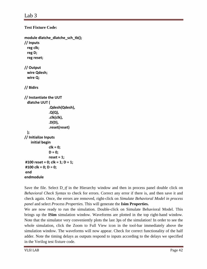
Test Fixture Code: module dlatche_dlatche_sch_tb(); // Inputs reg clk; reg D; reg reset; // Output wire Qdesh; wire Q; // Bidirs // Instantiate the UUT dlatche UUT ( .Qdesh(Qdesh), .Q(Q), .clk(clk), .D(D), .reset(reset) ); // Initialize Inputs initial begin clk = 0; D = 0; reset = 1; #100 reset = 0; clk = 1; D = 1; #100 clk = 0; D = 0; end endmodule Save the file. Select D_tf in the Hierarchy window and then in process panel double click on Behavioral Check Syntax to check for errors. Correct any error if there is, and then save it and check again. Once, the errors are removed, right-click on Simulate Behavioral Model in process panel and select Process Properties. This will generate the Isim Properties. We are now ready to run the simulation. Double-click on Simulate Behavioral Model. This brings up the ISim simulation window. Waveforms are plotted in the top right-hand window. Note that the simulator very conveniently plots the last 3ps of the simulation! In order to see the whole simulation, click the Zoom to Full View icon in the tool-bar immediately above the simulation window. The waveforms will now appear. Check for correct functionality of the half adder. Note the timing delays as outputs respond to inputs according to the delays we specified in the Verilog test fixture code.

Lab 3
VLSI LAB Page 43
Figure 2
LAB TASK # 2:
Design and simulate D-Flip-flop
D FLIP-FLOP: Latches are often called level-sensitive because their output follows their inputs as long as they are enabled. They are transparent during this entire time when the enable signal is asserted. There are situations when it is more useful to have the output change only at the rising or falling edge of the enable signal. This enable signal is usually the controlling clock signal. Thus, we can have all changes synchronized to the rising or falling edge of the clock. An edge-triggered flip-flop achieves this by combining in series a pair of latches. Figure shows a positive edge-triggered D flip-flop where two D latches are connected in series. The first latch is called the master latch. The master latch is enabled when Clk = 0 and follows the primary input D. When Clk is 1, the master latch is disabled but the second latch, called the slave latch, is enabled so that the output from the master latch is transferred to the slave latch. The slave latch is enabled all the while that Clk = 1, but its content changes only at the beginning of the cycle, that is, only at the rising edge of the signal because once Clk is 1, the master latch is disabled and so the input to the slave latch

Lab 3
VLSI LAB Page 44
will not change. The circuit is called a positive edge-triggered flip flop because the output Q on the slave latch changes only at the rising edge of the clock. If the slave latch is enabled when the clock is low, then it is referred to as a negative edge-triggered flip-flop. The circuit is also referred to as a master slave D flip-flop because of the two latches used in the circuit.
TRUTH TABLE Logic Symbol
Figure 3
Test Fixture Code: module D_FlipFlop_D_FlipFlop_sch_tb(); // Inputs reg D; reg Reset; reg Clk;

Lab 3
VLSI LAB Page 45
// Output wire Q; wire Qbar; // Bidirs // Instantiate the UUT D_FlipFlop UUT ( .D(D), .Q(Q), .Qbar(Qbar), .Reset(Reset), .Clk(Clk) ); parameter period =100; always begin Clk =1; #(period/2) Clk = 0; #(period/2); end initial begin D = 0; Reset = 1; #100 Reset = 0; D= 1; #90 D = 0; end endmodule Your task is completed successfully. Now add and explain the screen shot of your task design simulation.

Lab 3
VLSI LAB Page 46
LAB TASK # 3:
Design T Flip Flop using D Flip Flop
T FLIP FLOP:
The T flip-flop has one input in addition to the clock. T stands for toggle for the obvious reason. When T is asserted (T = 1), the flip-flop state toggles back and forth, and when T is de-asserted, the flip-flop keeps its current state. The T flip-flop can be constructed using a D flip-flop with the two outputs Q and Q'.
TRUTH TABLE
Figure 5
Test Fixture Code: module T_FlipFlop_T_FlipFlop_sch_tb(); // Inputs
T Q
0 0 0 1
0 1 1 0
1 0 1 0
1 1 0 1
LOGIC SYMBOL OF T FLIP FLOP

Lab 3
VLSI LAB Page 47
reg T; reg Clk; reg Reset; // Output wire Q; // Bidirs // Instantiate the UUT T_FlipFlop UUT ( .T(T), .Q(Q), .Clk(Clk), .Reset(Reset) ); parameter period =100; always begin Clk =1; #(period/2) Clk = 0; #(period/2); end // Initialize Inputs initial begin T = 1; Reset = 1; #100 Reset = 0; T= 1; end endmodule Your task is completed successfully. Now add and explain the screen shot of your task design simulation.
Lab 3
VLSI LAB Page 48
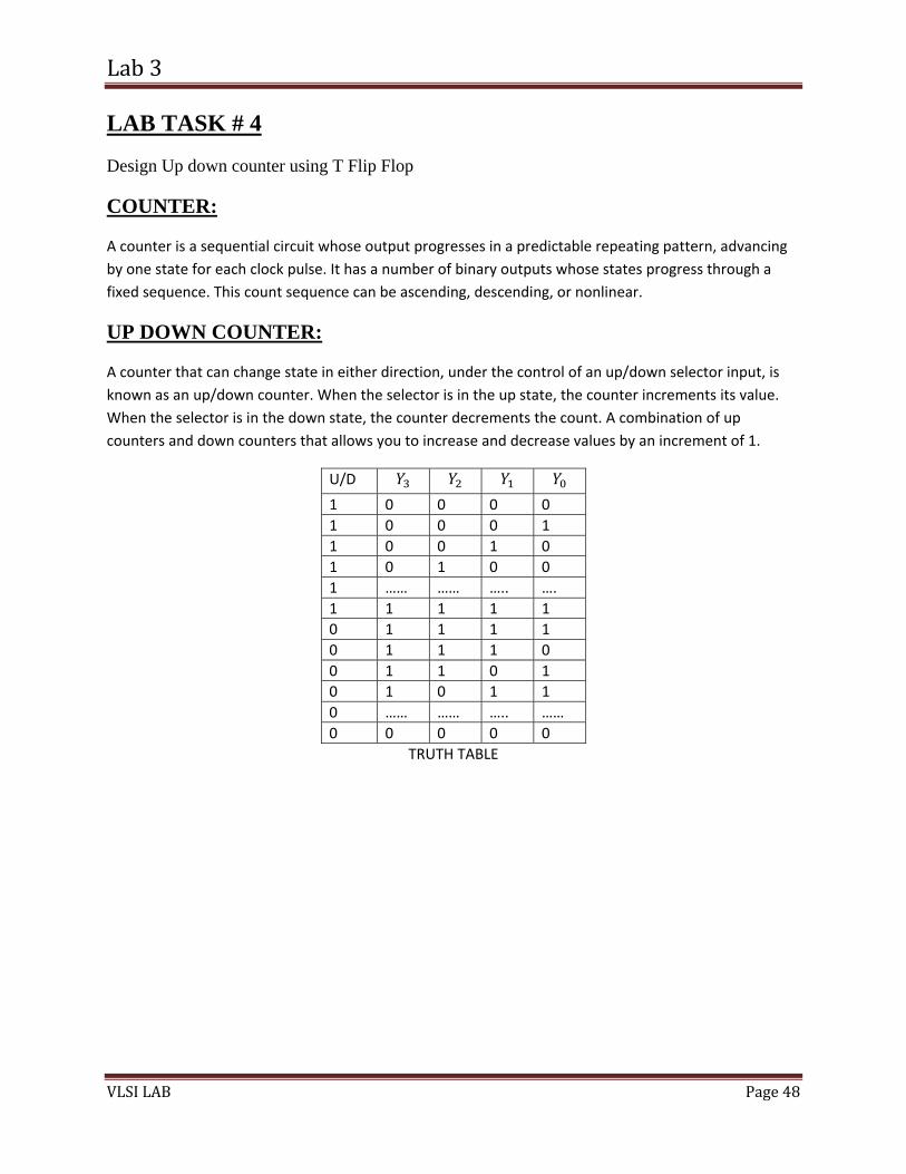
LAB TASK # 4
Design Up down counter using T Flip Flop
COUNTER:
A counter is a sequential circuit whose output progresses in a predictable repeating pattern, advancing by one state for each clock pulse. It has a number of binary outputs whose states progress through a fixed sequence. This count sequence can be ascending, descending, or nonlinear.
UP DOWN COUNTER:
A counter that can change state in either direction, under the control of an up/down selector input, is known as an up/down counter. When the selector is in the up state, the counter increments its value. When the selector is in the down state, the counter decrements the count. A combination of up counters and down counters that allows you to increase and decrease values by an increment of 1.
U/D
1 0 0 0 0 1 0 0 0 1 1 0 0 1 0 1 0 1 0 0 1 …… …… ….. …. 1 1 1 1 1 0 1 1 1 1 0 1 1 1 0 0 1 1 0 1 0 1 0 1 1 0 …… …… ….. …… 0 0 0 0 0
TRUTH TABLE

Lab 3
VLSI LAB Page 49
Figure 7
Test Fixture Code: module counter_counter_sch_tb(); // Inputs reg updown; reg Reset; reg Clk; // Output wire Q0; wire Q1; wire Q2; wire Q3; // Instantiate the UUT counter UUT ( .updown(updown), .Reset(Reset), .Clk(Clk), .Q0(Q0), .Q1(Q1), .Q2(Q2), .Q3(Q3)

Lab 3
VLSI LAB Page 50
); parameter period =100; always begin Clk =1; #(period/2) Clk = 0; #(period/2); end // Initialize Inputs initial begin updown = 1; Reset = 1; #100 Reset = 0; #900; end endmodule Your task is completed successfully. Now add and explain the screen shot of your task design simulation.
Lab 4
VLSI LAB Page 51
LAB 4 OBJECTIVE Introduction to Verilog Language, Gate Level Modeling and Example. THEORY
WHAT IS MODULE IN VERILOG
A module is the basic building block in Verilog. Just like functions and procedures in C or any other language, in verilog a module can be an element or a collection of lower-level design blocks
In Verilog, a module is declared by the keyword “module”. A corresponding keyword “endmodule” must appear at the end of the module definition Each module must have a module_name, which is the identifier for the module, and a
module_terminal_list, which describes the input and output terminals of the module. STRUCTURE OF MODULE IN VERILOG
module <module name> (<module_terminal_list>); ... <module internals> ... ... Endmodule
In verilog, the internals of module can be defined at four levels of abstraction. These levels are:
a) Behavioral level b) Data flow level c) Gate level d) Switch level WHAT IS INSTANCE IN VERILOG
In verilog, A module provides a template from which we can create actual objects
When a module is invoked, Verilog creates a unique object from the template Each object has its own name, variables, parameters, and I/O interface The process of creating objects from a module template is called instantiation,
and the objects are called instances module ripple_carry(<module_terminal_list>); full_adder fa(<module_terminal_list>);

Lab 4
VLSI LAB Page 52
endmodule module full_adder (<module_terminal_list>); <module internals> endmodule
LEXICAL CONVENTIONS
• Whitespace – Blank spaces, tabs and newlines, comprise the whitespace.
• Comments – A one-line comment starts with "//". – A multiple-line comment starts with "/*" and ends with "*/".
• Operators – Operators are of three types: unary, binary, and ternary.
• a = ~ b; // ~ is a unary operator. b is the operand • a = b && c; // && is a binary operator. b and c are operands • a = b ? c : d; // ?: is a ternary operator. b, c and d are operands
• Number Specification – Sized numbers are represented as <size> '<base format> <number>.
• 4’b1111 // This is a 4-bit binary number • 12’habc // This is a 12-bit hexadecimal number • 16’d255 // This is a 16-bit decimal number •
DATA TYPES
• Nets – Nets represent connections between hardware elements. – Nets are declared primarily with the keyword wire.
• wire a; // Declare net a for the above circuit • wire b, c; // Declare two wires b,c for the above circuit • wire d = 1’b0; // Net d is fixed to logic value 0 at declaration
• Registers – Registers represent storage data elements. – Register data types are commonly declared by the key word reg.
• reg reset; // declare a variable that can hold its value • Vectors
– Nets or reg data types can be declared as vectors. – If bit width is not specified, the default is scalar.
• wire a; // scalar net variable, default • wire [7:0] bus; // 8-bit bus • wire [31:0] busA, busB, busC; // 3 buses of 32-bit width • reg clock; // scalar register, default • reg [0:40] virtual_addr; // vector register, 41-bits wide

Lab 4
VLSI LAB Page 53
PORTS
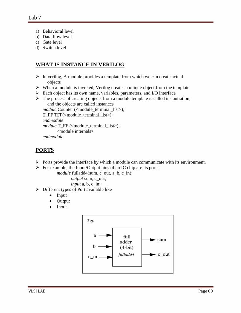
Ports provide the interface by which a module can communicate with its environment. For example, the Input/Output pins of an IC chip are its ports.
module fulladd4(sum, c_out, a, b, c_in); output sum, c_out; input a, b, c_in;
Different types of Port available like • Input • Output • Inout
PORT CONNECTION RULES • There are rules governing port connections when modules are instantiated within other
modules. • Inputs
– Internally, input ports must always be of the type net. Externally, the inputs can be connected to a variable which is a reg or a net.
• Outputs – Internally, outputs ports can be of the type reg or net. Externally, outputs must always
be connected to a net. They cannot be connected to a reg. • Inouts
– Internally, inout ports must be of the type net. Externally, inout ports must always be connected to a net.

Lab 4
VLSI LAB Page 54
SYSTEM TASKS AND COMPILER DIRECTIVES
• System tasks appear in the form $<keyword> • Displaying information
– $display is the main system task for displaying values of variables or strings or expressions. (%b, %h,%o,%s,%d,%c)
– Usage: $display(p1, p2, p3,....., pn); GATE-LEVEL MODELING
• Identify logic gate primitives provided in Verilog. • Understand instantiation of gates, gate symbols, and truth tables for AND, OR and NOT
type gates. • Understand how to construct a Verilog description from the logic diagram of the circuit. • Describe rise, fall, and turn-off delays in the gate-level design.
GATE TYPES

Lab 4
VLSI LAB Page 55
and and_1(out, in1, in2); and a1(out, in1, in2); or or_1(out, in1, in2); and a2(out, in1, in2, in3); nand nand_1( out, in1, in2); and a3(out, in1, in2, in3,in4); nor nor_1( out, in1, in2); xor xor_1( out, in1, in2); xnor xnor_1( out, in1, in2); GATE DELAYS • In real circuits, logic gates have delays associated with them. • Until now, we described circuits without any delays (i.e., zero delay). • There are three types of delays from the inputs to the output of a primitive gate.
– Rise, Fall, and Turn-off Delays
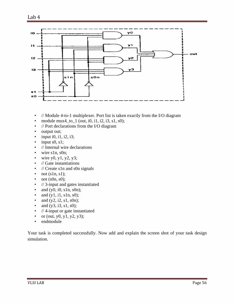
LAB TASK # 1 • GATE-LEVEL MULTIPLEXER
Lab 4
VLSI LAB Page 56
• // Module 4-to-1 multiplexer. Port list is taken exactly from the I/O diagram • module mux4_to_1 (out, i0, i1, i2, i3, s1, s0); • // Port declarations from the I/O diagram • output out; • input i0, i1, i2, i3; • input s0, s1; • // Internal wire declarations • wire s1n, s0n; • wire y0, y1, y2, y3; • // Gate instantiations • // Create s1n and s0n signals • not (s1n, s1); • not (s0n, s0); • // 3-input and gates instantiated • and (y0, i0, s1n, s0n); • and (y1, i1, s1n, s0); • and (y2, i2, s1, s0n); • and (y3, i3, s1, s0); • // 4-input or gate instantiated • or (out, y0, y1, y2, y3); • endmodule
Your task is completed successfully. Now add and explain the screen shot of your task design simulation.

Lab 4
VLSI LAB Page 57
LAB TASK # 2 • A 2-input XOR gate can be built from AND, OR and NOT gates. Construct an XOR gate
module in Verilog that realizes the logic function z = xy’ + x’y
Inputs are x and y, and z is the output. Your task is completed successfully. Now add and explain the screen shot of your task design simulation.

Lab 4
VLSI LAB Page 58
LAB ASSIGNMENT Lab Assignment 1: Implement the following circuit diagram OBSERVATION & RESULT:
__________________________________________________________________
__________________________________________________________________
__________________________________________________________________
__________________________________________________________________
__________________________________________________________________

Lab 4
VLSI LAB Page 59
Lab Assignment 2: Implement the 7 segment display logic circuit. OBSERVATION & RESULT:
__________________________________________________________________
__________________________________________________________________
__________________________________________________________________
__________________________________________________________________
__________________________________________________________________

Lab 5
VLSI LAB Page 60
LAB 5
OBJECTIVES Define expressions, operators, and operands. Use dataflow constructs to model practical digital circuits in Verilog.
THEORY
REASON FOR USING DATAFLOW MODELING
For small circuits, the gate-level modeling approach works very well. For small circuits, the gate-level modeling approach works very well The reason is that the number of gates is limited and the designer can instantiate and connect every gate individually but in complex designs the number of gates is very large. Thus, designers can design more effectively if they concentrate on implementing the function at a level of abstraction higher than gate level.
This is the point where Dataflow Modeling comes, provides a powerful way to implement a design.
IMPORTANCE OF DATAFLOW MODELING
Dataflow Modeling provides much easier platform for designing as compared to gate level because gate densities on chips increasing rapidly. In this context, even gate-level circuits are created using logic synthesis from a dataflow design description for maximum flexibility; gate-level, data flow, and behavioral design are used in combination.
CONTINUOUS ASSIGNMENT
The basic statement in dataflow modeling is continuous assignment .Its purpose is to drive value onto a net .This assignment replaces gates in the description of the circuit and describes the circuit at a higher level of abstraction .The keyword for continuous assignment is “assign ”
CHARACTERISTICS OF CONTINUOUS ASSIGNMENT
The left hand side of an assignment must always be a scalar or vector net or a concatenation of scalar and vector nets. It cannot be a scalar or vector register Continuous assignments are always active.
The assignment expression is evaluated as soon as one of the right-hand-side operands changes and the value is assigned to the left-hand-side net. The operands on the right-hand side can be registers or nets or function calls. Registers or nets can be scalars or vectors.
Lab 5
VLSI LAB Page 61
EXAMPLES
2 x 1 multiplexer
//method 1 module mux21(q, sel, a, b); input sel, a, b; output q; assign q = (~sel & a) | (sel & b); //assign q = sel ? b : a; endmodule //method 2 module mux21(q, sel, a, b); input sel, a, b; output q; assign q = (~sel & a) | (sel & b); endmodule EXPRESSIONS, OPERATORS AND OPERANDS
Dataflow modeling describes the design in terms of expressions instead of primitive gates
a) Expressions:
Expressions are constructs that combine operators and operands to produce a result.
b) Operands:
Operands can be constants, integers, real numbers, nets, registers.
c) Operators:
Operators act on the operands to produce desired results. Verilog provides various types of operators.

Lab 5
VLSI LAB Page 62

Lab 5
VLSI LAB
LAB T
CODE
// Modulemodule m// Port deoutput ouinput i0, input s0, assign ouendmodu CODE# // Modulemodule m
B
TASK # 1
#1:
e 4-to-1 mulmux4_to_1 (eclarations frut; i1, i2, i3; s1;
ut = s1 ? (s0ule
#2:
e 4-to-1 mulmux4_to_1 (
1
ltiplexer. Por(out, i0, i1, i2rom the I/O
0 ? i3 : i2):(s0
ltiplexer. Por(out, i0, i1, i2
rt list is take2, i3, s1, s0)diagram
0 ? i1 : i0) ;
rt list is take2, i3, s1, s0)
en exactly fro);
en exactly fro);
om the I/O d
om the I/O d
diagram
diagram
Page 63

Lab 5
VLSI LAB
// Port deoutput ouinput i0, input s0, assign ou(i3 & s0 endmodu Your tassimulatio
LAB T
B
eclarations frut; i1, i2, i3; s1;
ut = (i0 & (~& s1);
ule
k is compleon.
TASK # 2
rom the I/O
~s0) & (~s1)
ted successf
2
diagram
)) | (i1 & s0 &
fully. Now a
& (~s1)) | (i2
add and exp
2 & (~s0) &
plain the scre
& s1) |
een shot of
Pa
your task d
ge 64
design

Lab 5
VLSI LAB Page 65
CODE : // Module 2-bit Full Adder. Port list is taken exactly from the I/O diagram module fulladd2_bit(y, z, c, b, a); // Port declarations from the I/O diagram output y, z; input c, b, a; assign y = c ? (a?(b?1:0):(b?0:1)):(a?(b?0:1):(b?1:0)); assign z = (c ? (a?1:b):(a?(b?1:0):0)); endmodule Your task is completed successfully. Now add and explain the screen shot of your task design simulation.

Lab 5
VLSI LAB Page 66
LAB ASSIGNMENT Lab Assignment 1: Given below is the theory and logic of 8 bit Ripple Carry Adder / Subtractor. Your assignment is to design a 8 bit Ripple Carry Adder / Subtractor using Data flow Modeling record a truth table for this adder / subtractor. ADDER / SUBTRACTOR The adder / subtractor circuit performs subtraction by adding the negated value of the second operand. Recall that to negate a value in two’s complement representation, we simply invert all the bits from 0 to 1 and vice versa, and then add a 1. When the subtraction operation is selected, i.e. S = 1, the B operand needs to be inverted. Recalling that x 1 = x', we can thus simply flip the bits in B by performing the operation B S since S = 1. Finally, the addition of a 1 is accomplished by setting the primary carry-in signal c0 to 1. On the other hand, when the addition operation is selected, i.e. S = 0, the B operand will not be inverted by the XOR operation. In this case, we also want c0 = S = 0.
8-bit adder / subtractor combination circuit
Operation performed

Lab 5
VLSI LAB Page 67
OBSERVATION & RESULT:
__________________________________________________________________
__________________________________________________________________
__________________________________________________________________
__________________________________________________________________
__________________________________________________________________

LAB 6
VLSI LAB
LAB
OBJE
Introduct
THEO
BEHAV
Behaviortechniquesignals wThis is adesign, wusing twonly insid
THE C
Condition
• These• Keyw
1) SIMP
if (enableq <= d;
B
B 6 CTIVE
tion to behav
ORY
VIORAL M
ral modelinges are relativ
work. The aba very powerwhich is the
wo importantde these two
CONDITIO
nal statemen
e conditionswords if and
PLE IF ST
e)
vioral model
MODELI
g is the highevely detailedbstraction inrful abstractbasic inform
t constructs: o structured p
ONAL STA
nts are used f
are used to else are used
TATEMEN
ling.
ING
est level of d. They requ
n this modeltion techniqumation for an
initial and procedure co
ATEMEN
for making d
decide whetd for conditi
NT
abstraction iuire some kning is as simue. All that ny design .Malways. All
onstructs.
NT IF-ELS
decisions ba
ther or not a ional stateme
in the Verilonowledge of
mple as writdesigner ne
Most of the bl the other b
SE
sed upon cer
statement shents
og HDL. Thf how hardwting the logieeds are the behavioral mbehavioral s
rtain conditi
hould be exe
Pa
e other modware or hardic in C langualgorithm o
modeling, is tatements ap
ion
ecuted.
ge 68
deling dware uage.
of the done
ppear

LAB 6
VLSI LAB
2) ONE
if (reset q <= 0; else q <= d; 3) NES if (reset =counter <else if (encounter <else if (encounter <else counter < THE C
The caseone of tha case sta
If there akeywordCase statcasez treaunknowncasex) inconditionare repre
B
E ELSE ST
== 1'b1)
TED IF-E
== 1'b0) <= 4'b0000; nable == 1'b<= counter +nable == 1'b<= counter -
<= counter; /
CASE STA
e statement ihe expressionatement. The
are multiple ss .The defautement with ats high-imp
n (x) values an any bit of ens during thesented using
TATEMEN
ELSE-IF S
b1 && up_en+ 1'b1; b1 && down
1'b0;
// Redundant
ATEMENT
is a multi-wns and brance case statem
statements uult item is opdon't cares:
pedance valuas don't care
either the case comparisong the ? mark.
NT
STATEME
n == 1'b1)
n_en == 1'b1
t code
T
way decision ches accordi
ment syntax i
under a singlptional. casez and ca
ues (z) as dones. Don't-carese expressionn, and that b.
ENT
);
statement thingly. Keywis as follows
le match, the
asex n't cares. case values (z vn or the caseit position sh
hat tests whords case an
s.
en they are g
sex treats bovalues for cae items shall hall not be c
hether an expnd end case
grouped usin
oth high-impasez, z and x
be treated aconsidered. T
Pa
pression maare used to m
g begin, and
edance (z) avalues for s don't-care
The don't car
ge 69
atches make
d end
and
res

LAB 6
VLSI LAB Page 70
THE CASEZ AND CASEX STATEMENT
• Special versions of the case statement allow the x and z logic values to be used as "don't care“
• casez uses the z as the don't care instead of as a logic value • casex uses either the x or the z as don't care instead of as logic values EXAMPLE: casez (opcode) 4'b1zzz : out = a; // don't care about lower 3 bits 4'b01??: out = b; //the ? is same as z in a number 4'b001?: out = c; default: out = $display ("Error xxxx does matches 0000"); endcase STRUCTURED PROCEDURES
All procedures in the Verilog HDL are specified within one of the following four statements:
INITIAL (CONSTRUCT)
An initial block consists of a statement or a group of statements enclosed in begin... end or a single statement, which will be executed only once at simulation time 0. If there is more than one block they execute concurrently and independently. The initial block is normally used for initialization, monitoring, generating wave forms (e.g., clock pulses) and processes which are executed once in a simulation. An example of initialization and wave generation is given below

LAB 6
VLSI LAB Page 71
EXAMPLE
always@(posedgeclk) begin:D_FF if (reset == 1) q <= 0; else q <=d; end ALWAYS (CONSTRUCT) An always block is similar to the initial block, but the statements inside an always block will repeated continuously, in a looping fashion, until stopped by $finish or $stop.NOTE: the $finish command actually terminates the simulation where as $stop. Merely pauses it and awaits further instructions. Thus $finish is the preferred command unless you are using an interactive version of the simulator.One way to simulate a clock pulse is shown in the example below. Note, this is not the best way to simulate a clock. See the section on the forever loop for a better method.
EXAMPLE initial Begin clk = 0; reset = 0; enable= 0; data=0; end PROCEDURAL ASSIGNMENTS
• Procedural assignments update values of reg, integer, real, or time variables • The value placed on a variable will remain unchanged until another procedural assignment
updates the variable with a different value • The left-hand side of a procedural assignment <lvalue> can be a reg, integer, real, or time
register variable or a memory element • The right-hand side can be any expression that evaluates to a value
There are two types of procedural assignment statements: blocking and no blocking.
BLOCKING ASSIGNMENTS
• The = operator is used to specify blocking assignments. A blocking statement must be executed before the execution of the statements that follow it in a sequential block.

LAB 6
VLSI LAB
NON B
• Non-flow
SEQUE
• Bloctype
B
BLOCKIN
blocking sta
ENTIAL A
ck statementes of blocks:
NG ASSIG
atements allo
AND PAR
ts are used tosequential b
GNMENTS
ow you to sc
RALLEL B
o group multblocks and p
S
chedule assig
BLOCKS
tiple statemearallel block
Synthes
gnments with
Synthes
ents to act toks
sis Output
hout blockin
is Output
ogether as on
Pa
ng the proced
ne. There are
ge 72
dural
e two

LAB 6
VLSI LAB
SEQUE• The • Sequ• The • If de
state
Parallel
• The k• Paral• Statem
by th• If del
Block• fork: • join: j
Example
//parallelreg x,y; reg [1:0] Initial fork x = 1’b0;#5 y = 1’#10 z = (#20 w =
B
ENTIAL Bkeywords b
uential blocstatements i
elay or eventement in the
Blocks
keywords forllel blocks haments in a pe delay or evlay or event k, the order isplitting sinjoining inde
e
l block
z,w;
;\\ completes’b1; \\ compl(x,y); \\ comp(y,x); \\ com
BLOCKS egin and endks have the in a sequentit control is sblock comp
rk and join aave the follo
parallel blockvent control control is spin which the
ngle flow intoependent flow
s at simulatioletes at simupletes at sim
mpletes at sim
d are used tofollowing chial block arespecified, it ipleted execut
are used to gowing charack are executeassigned to
pecified, it ise statements o independews into singl
on time 0 ulation time 5mulation timemulation tim
o group stateharacteristicse processed iis relative to tion
group statemcteristics: ed concurreneach statem
s relative to tare written ient flows le flow
5 e 10
me 20
ements into ss: n the order tthe simulati
ments into seq
ntly Orderingment.
the time the is not import
sequential bl
they are specion time whe
quential bloc
g of stateme
block was etant.
Pa
locks
cified. en the previo
cks.
nts is contro
ntered in Pa
ge 73
ous
olled
arallel

LAB 6
VLSI LAB
join • The res
running
LAB T
Your tassimulatio
B
sult is that thg in parallel.
TASK#1:
k is compleon.
he simulation.
:
ted successf
n will end at
fully. Now a
t time 20 inst
add and exp
tead of time
plain the scre
35 b/c all st
een shot of
Pa
tatements are
your task d
ge 74
e
design
LAB 6
VLSI LAB
LAB T1) Write
the co
Your tassimulatio
B
TASK#2:e and verify ount at every
k is compleon.
: a verilog moy clock and u
ted successf
odel of up_dup_down_pt
fully. Now a
down_countetr.
add and exp
er the circuit
plain the scre
t that increm
een shot of
Pa
ment or decre
your task d
ge 75
ement
design
LAB 6
VLSI LAB
Lab As
3-bit up-activity.
OBS ____
____
____
____
____
B
ssignment
down count
SERVATI
_________
_________
_________
_________
_________
1:
er with addi
ION & RE
_________
_________
_________
_________
_________
LAB
itional featur
ESULT:
__________
__________
__________
__________
__________
ASSIGN
res that load
__________
__________
__________
__________
__________
NMENT
d an initial co
_________
_________
_________
_________
_________
ount and ena
_________
_________
_________
_________
_________
Pa
able the cou
_________
_________
_________
_________
_________
ge 76
unting
____
____
____
____
___

LAB 6
VLSI LAB
Lab As
Design k
OBS ____
____
____
____
____
B
ssignment
keypad Scann
SERVATI
_________
_________
_________
_________
_________
2:
ner and Enco
ION & RE
_________
_________
_________
_________
_________
oder.
ESULT:
__________
__________
__________
__________
__________
__________
__________
__________
__________
__________
_________
_________
_________
_________
_________
_________
_________
_________
_________
_________
Pa
_________
_________
_________
_________
_________
ge 77
____
____
____
____
___

Lab 7
VLSI LAB Page 78
LAB 7
OBJECTIVE: Hierarchal model. THEORY:
DESIGN METHODOLOGY:
Basically there are two types of design methodologies:
a) Top-down methodology
Bottom-up methodology
In a top-down design methodology, we define the top-level block and identify the sub-blocks necessary to build the top-level block
In a bottom-up design methodology, we first identify the building blocks that are available to us. We build bigger cells, using these building blocks

Lab 7
VLSI LAB Page 79
In common applications, a combination of top-down and bottom-up methodology is used
WHAT IS MODULE IN VERILOG
A module is the basic building block in Verilog. Just like functions and procedures in C
or any other language, in verilog a module can be an element or a collection of lower-level design blocks
In Verilog, a module is declared by the keyword “module”. A corresponding keyword “endmodule” must appear at the end of the module definition Each module must have a module_name, which is the identifier for the module, and a
module_terminal_list, which describes the input and output terminals of the module.
WHAT IS MODULE IN VERILOG
A module is the basic building block in Verilog. Just like functions and procedures in C or any other language, in verilog a module can be an element or a collection of lower-level design blocks
In Verilog, a module is declared by the keyword “module”. A corresponding keyword “endmodule” must appear at the end of the module definition Each module must have a module_name, which is the identifier for the module, and a
module_terminal_list, which describes the input and output terminals of the module.
STRUCTURE OF MODULE IN VERILOG module <module name> (<module_terminal_list>); ... <module internals> ... ... Endmodule
In verilog, the internals of module can be defined at four levels of abstraction. These levels are:
Lab 7
VLSI LAB Page 80
a) Behavioral level b) Data flow level c) Gate level d) Switch level
WHAT IS INSTANCE IN VERILOG
In verilog, A module provides a template from which we can create actual objects
When a module is invoked, Verilog creates a unique object from the template Each object has its own name, variables, parameters, and I/O interface The process of creating objects from a module template is called instantiation,
and the objects are called instances module Counter (<module_terminal_list>); T_FF TFF(<module_terminal_list>); endmodule module T_FF (<module_terminal_list>); <module internals> endmodule
PORTS
Ports provide the interface by which a module can communicate with its environment. For example, the Input/Output pins of an IC chip are its ports.
module fulladd4(sum, c_out, a, b, c_in); output sum, c_out; input a, b, c_in;
Different types of Port available like • Input • Output • Inout

Lab 7
VLSI LAB Page 81
DATA TYPES
Value Set Verilog supports four values
Value Level Condition in Hardware Circuits
0 Logic zero, false condition
1 Logic one, true condition
X Unknown logic value
Z High impedance, floating state
A PRACTICAL EXAMPLE
We can take a practical example of 4-bit Ripple Carry Counter for verilog module
We are using bottom-up methodology for the design

Lab 7
VLSI LAB Page 82
LAB TASK # 1:
Step one is to design a D-FlipFlop Truth table for D-FlipFlop Verilog module for D-flipflop
module D_FF(q, d, clk, reset); output q; input d, clk, reset; reg q; always @ ( posedge clk or negedge reset) if (~reset) begin q <= 1'b0; end else begin q <= data; end endmodule
Your task is completed successfully. Now add and explain the screen shot of your task design simulation.
LAB TASK # 2:
Step one is to Design T-flipflop using D-flipflop and inverter Schematic for T-FlipFlop Verilog module for T-flipflop
module T_FF(q, clk, reset); output q; input clk, reset; wire d;

Lab 7
VLSI LAB Page 83
D_FF dff0(q, d, clk, reset); not n1(d, q); // not is a Verilog-provided primitive. case sensitive endmodule
Your task is completed successfully. Now add and explain the screen shot of your task design simulation.
LAB TASK # 3:
Design Ripple Carry Counter using four T-FlipFlop Verilog module for Ripple Carry Counter
module ripple_carry_counter(q, clk, reset); output [3:0] q; input clk, reset; //4 instances of the module T_FF are created. T_FF tff0(q[0],clk, reset); T_FF tff1(q[1],q[0], reset); T_FF tff2(q[2],q[1], reset); T_FF tff3(q[3],q[2], reset); Endmodule

Lab 7
VLSI LAB Page 84
Your task is completed successfully. Now add and explain the screen shot of your task design simulation.

Lab 7
VLSI LAB Page 85
LAB ASSIGNMENTS Lab Assignment 1: The theory of SIPO (serial in parallel out) 4 bit shift register is given below, your assignment is to design and simulate and record the output in the form of truth table. SIPO:
This configuration allows conversion from serial to parallel format. Data is input serially, Once the data has been input, it may be either read off at each output simultaneously, or it can be shifted out and replaced.
OBSERVATION & RESULT:
__________________________________________________________________
__________________________________________________________________
__________________________________________________________________
__________________________________________________________________
__________________________________________________________________

Lab 7
VLSI LAB Page 86
Lab Assignment 2: The theory of PISO (parallel in serial out) 4 Bit shift register is given below, your assignment is to design and simulate and record the output in the form of truth table. PISO:
This configuration has the data input on lines D1 through D4 in parallel format. To write the data to the register, the Write/Shift control line must be held LOW. To shift the data, the W/S control line is brought HIGH and the registers are clocked. The arrangement now acts as a SISO shift register, with D1 as the Data Input. However, as long as the number of clock cycles is not more than the length of the data-string, the Data Output, Q, will be the parallel data read off in order.
OBSERVATION & RESULT:
__________________________________________________________________
__________________________________________________________________
__________________________________________________________________
__________________________________________________________________
__________________________________________________________________

Lab 9
VLSI LAB
LAB OBJETo studygates del
THEO • In re• Veri• Gate• Ther
a)b)
RISE DE
The rise
FALL D
The fall d
B
B 9 CTIVE:
y the characteays.
ORY:
eal circuits, lilog providese delays allore are three t) Rise, Fall) Minimal,
ELAY
delay is asso
DELAY
delay is asso
eristics of lo
logic gates hs the mechanw the Verilotypes of delal and Turn-oTypical, and
ociated with
ociated with
ogic gates de
haves delays nism to assoog user to spays from theff delays. d Maximum
a gate outpu
a gate outpu
elays and to c
associated wociate delayspecify delays inputs to th
m delays.
ut transition
ut transition t
calculate and
with them. with gates.
s through thee output of a
to a 1 from
to a 0 from a
d measure th
e logic circuia primitive g
another valu
another valu
Pa
he output of
its. gate:
ue.
ue.
ge 87
logic

Lab 9
VLSI LAB Page 88
TURN OFF DELAY
• The turn-off delay is associated with a gate output transition to the high impedance value (z) from another value.
• Three types of delay specifications are allowed: • If only one delay is specified, this value is used for all transitions. • If two delays are specified, they refer to the rise and fall delay values. • If all three delays are specified, they refer to rise, fall, and turn-off delay Values. • The turn-off delay is the minimum of the two delays.
Examples
// Delay for all transitions or #5 u_or (a,b,c); // Rise and fall delay and #(1,2) u_and (a,b,c); // Rise, fall and turn off delay nor # (1,2,3) u_nor (a,b,c); //One Delay, min, typ and max nand #(1:2:3) u_nand (a,b,c); //Two delays, min,typ and max buf #(1:4:8,4:5:6) u_buf (a,b); //hree delays, min, typ, and max notif1 #(1:2:3,4:5:6,7:8:9) u_notif1 (a,b,c); LOOPING STATEMENTS Verilog has four looping statements like any other programming language.
• forever • repeat • while • for
All looping statements can appear only inside an initial or always block. Loops may contain delay expressions.

Lab 9
VLSI LAB Page 89
THE FOREVER STATEMENT
The forever loop executes continually, the loop never ends
syntax : forever <statement>
Example
Free running clock generator initial begin clk = 0; forever #5 clk = !clk; end THE REPEAT STATEMENT
The repeat loop executes statement fixed <number> of times
syntax : repeat (<number>) <statement>
Example if (opcode == 10) //perform rotate repeat (8) begin temp = data[7]; data = {data<<1,temp}; end
THE WHILE LOOP STATEMENT The while loop executes as long as an <expression> evaluates as true
syntax : while (<expression>) <statement>
Example
loc = 0; if (data = 0) // example of a 1 detect shift value loc = 32; else while (data[0] == 0); //find the first set bit begin loc = loc + 1; data = data << 1; end

Lab 9
VLSI LAB Page 90
THE FOR LOOP STATEMENT
• The For loop is same as the For loop used in any other programming language. • Executes an <initial assignment> once at the start of the loop. • Executes the loop as long as an <expression> evaluates as true. • Executes a <step assignment> at the end of each pass through the loop.
Syntax
for (<initial assignment>; <expression>, <step assignment>)
<statement>
Example for (i=0;i<=63;i=i+1) ram[i] <= 0; // Inialize the RAM with 0
PROCEDURAL TIMING CONTROL
• Delays controls. • Edge-Sensitive Event controls • Level-Sensitive Event controls-Wait statements • Named Events
DELAYS CONTROLS Delays the execution of a procedural statement by specific simulation time. syntax : #<time> <statement>;
Example
module clk_gen (clk,reset); output clk,reset; reg clk, reset; initial begin clk = 0; reset = 0; #2 reset = 1; #5 reset = 0; end always #1 clk = !clk; Endmodule

Lab 9
VLSI LAB Page 91
EDGE SENSITIVE EVENT CONTROLS Delays execution of the next statement until the specified transition on a signal.
syntax : @ (<posedge>|<negedge> signal) <statement>;
Example
always @ (posedge enable) begin repeat (5) // Wait for 5 clock cycles @ (posedge clk) ; trigger = 1; end
LEVEL-SENSITIVE EVEN CONTROLS ( WAIT STATEMENTS ) Delays execution of the next statement until the <expression> evaluates as true.
syntax : wait (<expression>) <statement>;
Example
while (mem_read == 1'b1) begin wait (data_ready) data = data_bus; read_ack = 1; end

Lab 9
VLSI LAB
Lab As
Use a forcan overl
OBSER
_______
_______
_______
_______
_______
B
ssignment
r loop to detelap each othe
RVATION
_________
_________
_________
_________
_________
1:
ect number oer, ex. 01010
N & RESU
_________
_________
_________
_________
_________
LAB AS
of times ‘0100 counts as t
ULT:
_________
_________
_________
_________
_________
SSIGNME
0’ pattern is two patterns
_________
_________
_________
_________
_________
ENTS
found in a 3. The 4-bit o
_________
_________
_________
_________
_________
32-bit input doutput is nam
__________
__________
__________
__________
__________
Pa
din. The pattmed count
_________
_________
_________
_________
_________
ge 92
terns
___
___
___
___
___

Lab 9
VLSI LAB
Lab As Use whilholds the
Hint
• U• Y
OBSER
_______
_______
_______
_______
_______
B
ssignment
le loop to dee result of the
Use successivYou can assu
RVATION
_________
_________
_________
_________
_________
2:
sign a circuie division, a
ve subtractioume that din
N & RESU
_________
_________
_________
_________
_________
it which diviand 2-bit outp
ons to get theis always a p
ULT:
_________
_________
_________
_________
_________
ides a 16-bitput remaind
e result and tpositive num
_________
_________
_________
_________
_________
t input din byer the remain
the remaindember.
_________
_________
_________
_________
_________
y 3. The 15-bnder.
er.
__________
__________
__________
__________
__________
Pa
bit output re
_________
_________
_________
_________
_________
ge 93
esult
___
___
___
___
___

Lab 10
VLSI LAB Page 94
LAB 10 OBJECTIVE: State Machines THEORY: STATE MACHINE: An event is an occurrence of a phenomenon at a certain moment in time. The occurrence of the event itself is assumed to have no duration. Typically, when an event occurs, it affects the state of an object. A state machine is a model of the behavior of a single object over time and helps you to understand how that object's state affects its reactions to events. There are two types of state machines: Mealy machines and Moore machines. You can model both types of machines in Verilog. MOORE MACHINES: In a Moore machine, the outputs are a function of the current state. This implies that the outputs from the Moore machine are synchronous to the state changes. In moore, it has to wait for one clock cycle since it changes with the state.
Moore State Machine
MEALY MACHINES: In a Mealy machine, the outputs are a function of both the state and the inputs. Mealy will be faster. In the sense that,output will change as soon as the input transition according to the logic.

Lab 10
VLSI LAB Page 95
Mealy State Machine
A state machine can be broken down into three parts: The state register, the next state logic, and the output logic. A state machines can be depicted as shown in Figure below: LAB TASK # 1: Designs a vending machine in which the following action are perform: • Release item after 15 cents are deposited • Single coin slot for dimes, nickels • No change The diagram is shown below:

Lab 10
VLSI LAB Page 96
Suitable Abstract Representation for the Moore machine is: • Tabulate typical input sequences:
o 3 nickels o nickel, dime o dime, nickel o two dimes
• Draw state diagram:
o Inputs: N, D, reset o Output: open chute
• Assumptions: o Assume N and D asserted for one cycle o Each state has a self loop for N = D = 0 (no coin)
Let’s start with the following steps:
CREATING A PROJECT FOR MOORE MACHINE:
The software we will be using is the Xilinx "ISE Project Navigator", in which you can enter the Schematic design and simulate its outputs for a specified sequence of inputs. To start up, go to Start All Programs Xilinx ISE Design Suite 13.4 ISE Design Tools Project Navigator
The screen shown in Figure 1 appears.

Lab 10
VLSI LAB
At this pfiles, incauxiliaryYou can Wizard aWe woul(C:\ projyou to th
0
B
point, you haluding schem
y files relatedeither click as shown in ld suggest yect_name) t
he Design Pr
ave not yet cmatic file thd to simulatio
New ProjecFigure 2. En
you create thto avoid addroperties po
created any hat define thons and othect or go to Fnter a projec
he project in ding lots of np-up as show
Figure 1
project so whe circuit comer parts of th
File -> New ct name and l
the "My Donew files inwn in Figure
we will startmponents an
he design perProject. Thlocation. ocuments" f
nto your maie 3.
t here. A "prnd overall cirformed.
his launches
folder, ratherin 2 director
Pa
roject" is a sircuit, along
the New Pr
r than the dery. This will
ge 97
set of with
roject
efault l take

Lab 10
VLSI LAB
0
B
Figure 2
Page 98

Lab 10
VLSI LAB
In the DeThis is nsynthesisyou click From thethe New sources tto projecClick Neappears.
0
B
esign Properneeded whens stage needk OK, a Proj
e Project NaSource Wi
to your desigct" should beext, skip the
rties windown you reach tds to know tject Summa
avigator’s puizard as shogn. Select "Ve checked. Tinputout pu
w, you can sthe "synthesthe internal ary window
ull-down meown in FiguVerilog ModThe locationut pin wizar
Figure 3
specify the Dis" stage in design of thwill pop-up.
enus, select ure 4. This wdule" and addn should apprd and click
Device Familthe design a
he specific p. Click Finis
Project -> window can d the name opear as the d
next and th
ly and the Dand implemeprogrammabsh.
New Sourcbe used to
of your circudirectory youhe screen sh
Pa
evice. entation sincble device. W
ce. This launadd a varie
uit. The box u selected abhown in Figu
ge 99
ce the When
nches ety of "Add bove. ure 5

Lab 10
VLSI LAB
0
B
FFigure 4
Pagee 100

Lab 10
VLSI LAB
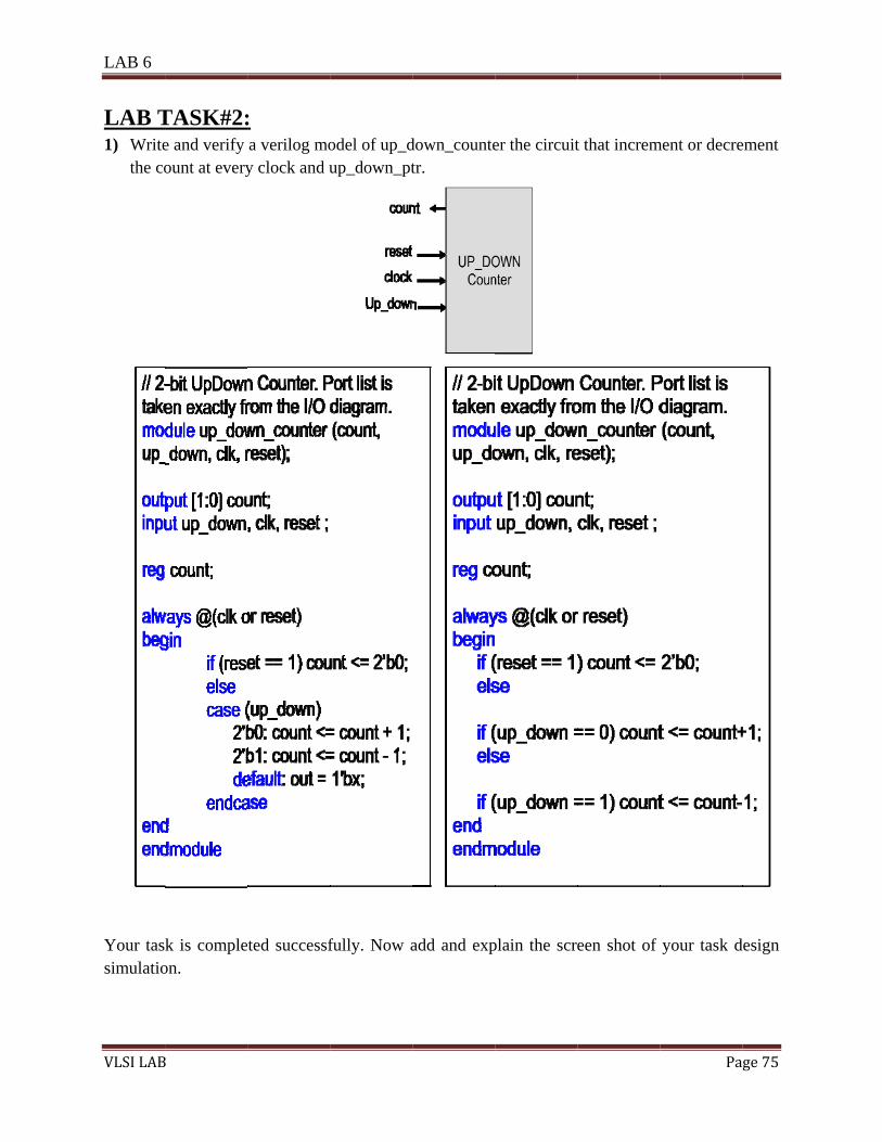
Now here module V output o input cl input re input N input Dreg openreg [1:0]reg [1:0]parametalways @case (stazero: begif (N) neelse if (Delse nextopen1 = end
0
B
e you can writ
Vending_M
open1; k;
eset; ; ;
n1; ] state; // sta] next_stateter zero = 0,@(N or D orate) gin xt_state = fi
D) next_statet_state = zer0;
te the followin
Moore( open
ate register ; , five = 1, ter state)
five; e = ten; ro;
ng verilog co
1, clk,reset,
n = 2, fiftee
Figure 5
ode for moore
N,D);
n = 3;
state machinne:
Pagee 101

Lab 10
VLSI LAB Page 102
five: begin if (N) next_state = ten; else if (D) next_state = fifteen; else next_state = five; open1 = 0; end ten: begin if (N) next_state = fifteen; else if (D) next_state = fifteen; else next_state = ten; open1 = 0; end fifteen: begin if (!reset) next_state = fifteen; else next_state = zero; open1 = 1; end endcase always @(posedge clk) if (reset || (!N && !D)) state <= zero; else state <= next_state; endmodule Save file and expand Synthesize XST in process window at the left of the window. Click on Check Syntax. If appears, your file completed successfully. CREATING VERILOG TEST FIXTURE MODULE FOR MOORE MACHINE: Select from the Project Navigator window Project -> New Source. The same New Source Wizard (Figure 4) appears that was used earlier to enter our Verilog module. This time, instead of selecting Verilog Module, select Verilog Test Fixture. Name the file state_tf (to distinguish it from the actual state file) and click Next. New windows will pop-up asking you which file describes the circuit you want to test. Select the file and then click Next. The New Source Wizard now shows a summary page. Click Finish. Clicking on Finish, the Project Navigator screen reappears and you will see that the wizard has already generated some more code, for a new entity called state_tf as shown in Figure 6. There may be some compiler errors that appear in the console window. Ignore them because we are

Lab 10
VLSI LAB Page 103
going to edit this file. It is not necessary for you to understand the semantics of this entity at this stage. Simply write the following code. module stat_tf; // Inputs reg clk; reg reset; reg N; reg D; // Outputs wire open1; // Instantiate the Unit Under Test (UUT) Vending_Moore uut ( .open1(open1), .clk(clk), .reset(reset), .N(N), .D(D) ); parameter PERIOD=100; always begin clk=1; #(PERIOD/2) clk=0; #(PERIOD/2); end initial begin // Initialize Inputs reset = 1; N = 0; D = 0; // Wait 100 ns for global reset to finish #100 reset = 0; N=1; D=0; #100 N=0; D=1; #100 N=0; D=0; end endmodule Save the file and expand ISim Simulator. Double click on Behavioral Check Syntax. When there is no error, a appears next to it, click Simulate Behavioral Mode, ISim (0.87xd)

Lab 10
VLSI LAB
window figure 7.
Now cheobjective
LAB T Design Mealy m Up till noAnd moreAnd writmachine. module v input Clreg openreg next_ paramet
0
B
appear in wVerify the o
eck and verof this task a
TASK # 2
the same vmachines.
w you can une machines. Nte the follow
vending_Me
k, Reset, N,n; reg state; _state; reg n
ter zero = 0,
which input aoutput.
rify the outplso add and e
2:
vending ma
nderstand the Now follow thwing code in
ealy (open,
, D; output // state regi
next_open;
, five = 1, te
and output w
put, also tabexplain the s
achine mech
difference behe same steps n Verilog mo
Clk, Reset,
open; ister
n = 2, fiftee
waves are sh
Figure 6
bulate the tscreen shot o
hanism wit
etween mealy as in task 1
odule for thi
N, D);
n = 3;
hown with N
ypical input
of your task
th
is
Name and V
sequences a
design simu
Page
Vales as show
as describe i
ulation.
e 104
wn in
n the

Lab 10
VLSI LAB Page 105
always @(N or D or state) case (state)
zero: begin if (N) begin
next_state = five; next_open = 0; end
else if (D) begin next_state = ten; next_open = 0; end
else begin next_state = zero; next_open = 0; end
end
five: begin if (N) begin
next_state = ten; next_open = 0; end
else if (D) begin next_state = fifteen; next_open = 1; end
else begin next_state = five; next_open = 0; end
end
ten: begin if (N) begin
next_state = fifteen; next_open = 1; end
else if (D) begin next_state = fifteen; next_open = 1; end
else begin next_state = ten; next_open = 0; end
end
fifteen: begin if (!Reset) next_state = fifteen; else next_state = zero; next_open = 1; end
endcase always @(posedge clk)

Lab 10
VLSI LAB Page 106
if (Reset || (!N && !D)) begin state <= zero; open <= 0; end else begin state <= next_state; open <= next_open; end endmodule CREATING A VERILOG TEST FIXTURE FOR MEALY MACHINE: Follow the same steps as in previous labs for the simulation part and write the following code in Verilog test fixture and verify the output according to the typical input sequence as describe in task 1. module Mealy_tf; // Inputs reg Clk; reg Reset; reg N; reg D; // Outputs wire open1; // Instantiate the Unit Under Test (UUT) Vending_Mealy uut ( .open1(open1), .Clk(Clk), Reset(Reset), .N(N), .D(D) ); parameter PERIOD=100; always begin Clk=1; #(PERIOD/2) Clk=0; #(PERIOD/2); end initial begin // Initialize Inputs Reset = 1; N = 0; D = 0; // Wait 100 ns for global reset to finish #100 Reset=0; N=1; D=0;

Lab 10
VLSI LAB Page 107
#100 N=0; D=1; #100 N=1; D=0; #100 N=0; D=0; end endmodule
Now check and verify the output, also tabulate the typical input sequences as describe in the objective of this task also add and explain the screen shot of your task design simulation.

Lab 10
VLSI LAB Page 108
LAB ASSIGNMENTS Lab Assignment: Traffic light controller. A busy highway is intersected by a little used farmroad • Detectors C sense the presence of cars waiting on the farmroad • with no car on farmroad, light remain green in highway direction • if vehicle on farmroad, highway lights go from Green to Yellow to Red, allowing the
farmroad lights to become green • these stay green only as long as a farmroad car is detected but never longer than a set interval • when these are met, farm lights transition from Green to Yellow to Red, allowing highway to
return to green even if farmroad vehicles are waiting, highway gets at least a set interval as green
Assume you have an interval timer that generates: • a short time pulse (TS) and • a long time pulse (TL), • in response to a set (ST) signal. • TS is to be used for timing yellow lights and TL for green lights Highway/farm road intersection is shown as follows:
Tabulation of Inputs and Outputs

Lab 10
VLSI LAB Page 109
Inputs Description Outputs Description reset place FSM in initial state HG, HY, HR assert green/yellow/red
highway lights C detect vehicle on the farm road FG, FY, FR assert green/yellow/red
highway lights TS short time interval expired ST start timing a short or long
interval TL long time interval expired
Tabulation of unique states – some light configurations imply others state description S0 highway green (farm road red) S1 highway yellow (farm road red) S2 farm road green (highway red) S3 farm road yellow (highway red) State Diagram is shown below:
Consider state assignments:
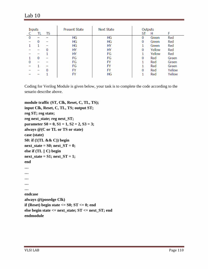
Lab 10
VLSI LAB Page 110
Coding for Verilog Module is given below, your task is to complete the code according to the senario describe above. module traffic (ST, Clk, Reset, C, TL, TS); input Clk, Reset, C, TL, TS; output ST; reg ST; reg state; reg next_state; reg next_ST; parameter S0 = 0, S1 = 1, S2 = 2, S3 = 3; always @(C or TL or TS or state) case (state) S0: if (!(TL && C)) begin next_state = S0; next_ST = 0; else if (TL || C) begin next_state = S1; next_ST = 1; end … … … … … endcase always @(posedge Clk) if (Reset) begin state <= S0; ST <= 0; end else begin state <= next_state; ST <= next_ST; end endmodule

Lab 10
VLSI LAB Page 111
OBSERVATION & RESULT: __________________________________________________________________
__________________________________________________________________
__________________________________________________________________
__________________________________________________________________
_______________________________________________________________

Lab 11
VLSI LAB Page 112
LAB 11
OBJECTIVES Introduction to Virtex 5 Development System.

Lab 11
VLSI LAB Page 113
THEORY
Xilinx Virtex 5 Development Kit Specification
• Xilinx Virtex®-5 LX50T FPGA in a 1136-pin BGA package
• 256Mbyte DDR2 SODIMM with 64-bit wide data
• 10/100/1000 Ethernet PHY and RS-232 serial port
• Multiple USB2 ports for programming, data transfer, and hosting applications
• HDMI video with resolution up to 1600x1200 & 24-bit color.
• AC-97 Codec with 48KHz sampling and line-in, line-out, microphone and headphone ports
• Real time power monitors on all power rails
• 32Mbyte Numonyx® StrataFlash for configuration and user-data storage
• 100MHz fixed oscillator and (up to) 400MHz programmable clock generator
• 112 FPGA I/O’s routed to expansion connectors (two high-speed parallel VHDC connectors and four 8-pin headers)
• GPIO includes 8 LEDs, 2 buttons, two-axis navigation switch, 8 slide switches, and a 16x2 character LCD
• 20W power supply, USB cable, and protective plexiglass covers

Lab 11
VLSI LAB Page 114
LAB TASK # 1:
Objective- Design Parallel to serial converter in Xilinx ISE 13.4 environment using Verilog HDL.
1. Starting the ISE Software

Lab 11
VLSI LAB Page 115
2. Create New Project

Lab 11
VLSI LAB Page 116
3. Project Name & Working Directory

Lab 11
VLSI LAB Page 117
4. Select Spartan 3E Starter Board

Lab 11
VLSI LAB Page 118
5. Add New Design Source File

Lab 11
VLSI LAB Page 119
6. Verilog HDL Source File View
7. Write Verilog HDL Code
Write the following Verilog Code in the editor
module Parallel_To_Serial(clk, reset, strobe, data_in, data_out); input [3:0] data_in; input clk, reset, strobe; output data_out; wire data_out; reg [3:0] temp_data; always @(posedge clk) begin if(reset) temp_data <= 4'b0000; else if(strobe) temp_data <= data_in; else temp_data[3:0] <= {temp_data[2:0],1'b0}; end assign data_out = temp_data[3]; endmodule Write these lines before endmodule and Save the “Parallel_To_Serial.v” file

Lab 11
VLSI LAB Page 120
8. Verilog HDL Source File View
9. Check Syntax
• Checking the Syntax of the New Parallel_to_Serial ModuleVerify that Implementation is selected at the top of design window.
• Select the Parallel_to_Serial design source in the Sources window to display the related processes in the Processes window.
• Click the “+” next to the Synthesize-XST process to expand the process group. • Double-click the Synthesize-XST process. • Close the HDL file.

Lab 11
VLSI LAB Page 121

Lab 11
VLSI LAB Page 122

Lab 11
VLSI LAB Page 123
10. Perform Behavioral Simulation
• Verifying Functionality using Behavioral Simulation
• Create the test bench as follows:
– Select the Parallel_To_Serial HDL file in the Sources window.
– Create a new test bench source by selecting Project → New Source.
– In the New Source Wizard, select Verilog Test Fixture as the source type, and type ParallelToSerialConverter_TB in the File Name field.
– Click Next.
11. Behavioral Simulation

Lab 11
VLSI LAB Page 124

Lab 11
VLSI LAB Page 125
12. Select Design for Behavioral Simulation • The Associate Source page shows that you are associating the test bench with the source file
Parallel_To_Serial. Click Next. • The Summary page shows that the source will be added to the project, and it displays the
source directory, type and name. Click Finish.
Associate Source

Lab 11
VLSI LAB Page 126
13. Test Bench Summary

Lab 11
VLSI LAB Page 127
14. Verilog Simulation Construct

Lab 11
VLSI LAB Page 128
Clock Declaration
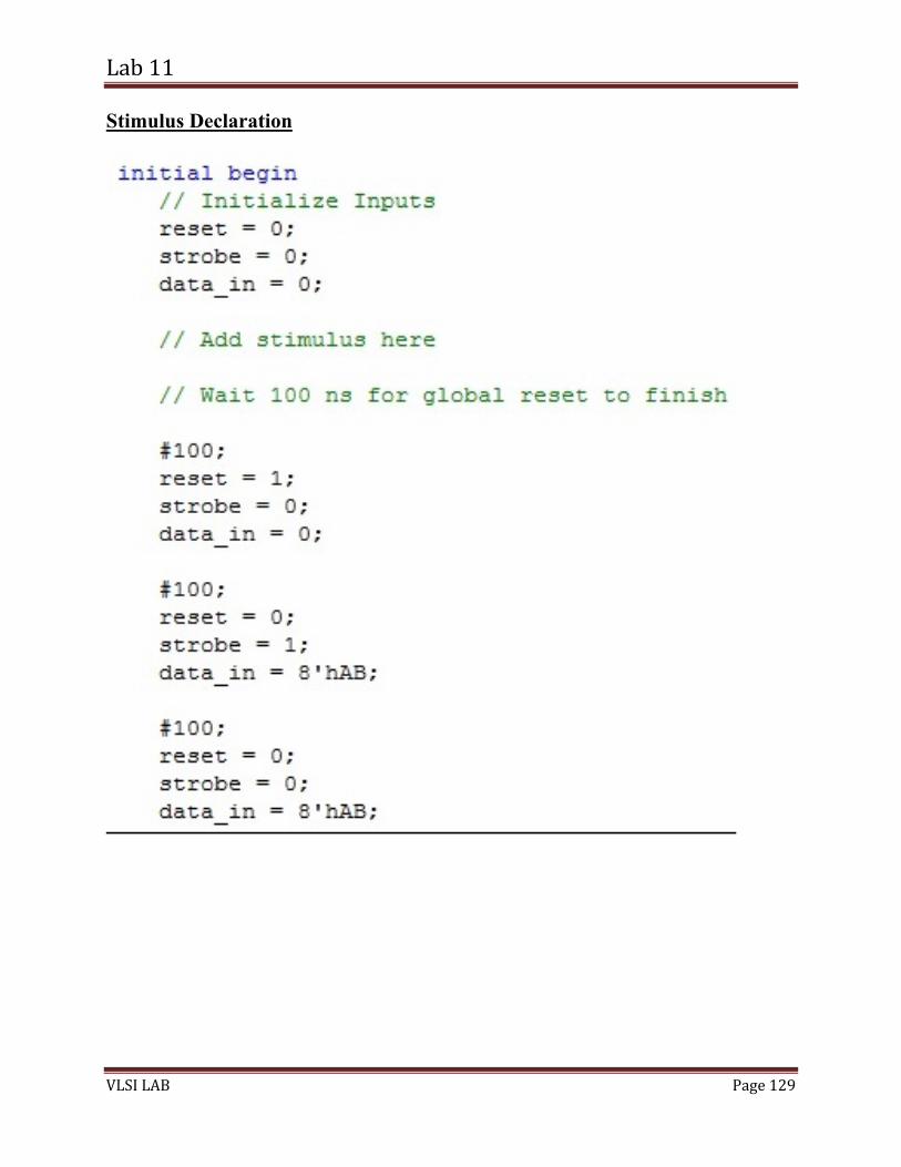
Lab 11
VLSI LAB Page 129
Stimulus Declaration

Lab 11
VLSI LAB Page 130
Simulate the Design
• Simulating Design Functionality
– Verify that Behavioral Simulation and ParallelToSerialConverter_TB are selected in the Sources window.
– In the Processes tab, click the “+” to expand the ISim Simulator process and double-click the Behavioral Check Syntax process.
– Then double-click on the Simulate Behavioral Model
– The ISE Simulator opens and runs the simulation to the end of the test bench.
Test Fixture File Syntax Check
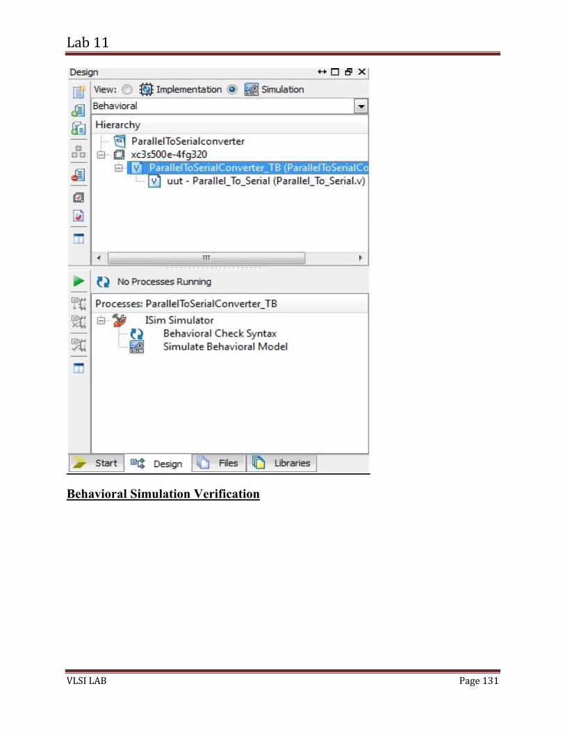
Lab 11
VLSI LAB Page 131
Behavioral Simulation Verification

Lab 11
VLSI LAB Page 132
15. Implementing the Design

Lab 11
VLSI LAB Page 133
• After simulation verification, we will implement design on FPGA.
• Select the Parallel_To_Serial source file in the Sources window.
• Double-click the Implement Design process in the Processes tab.
• Notice that after Implementation is complete, the Implementation processes have a green check mark next to them indicating that they completed successfully without errors or warnings.
Design Implementation
View Pinout Report
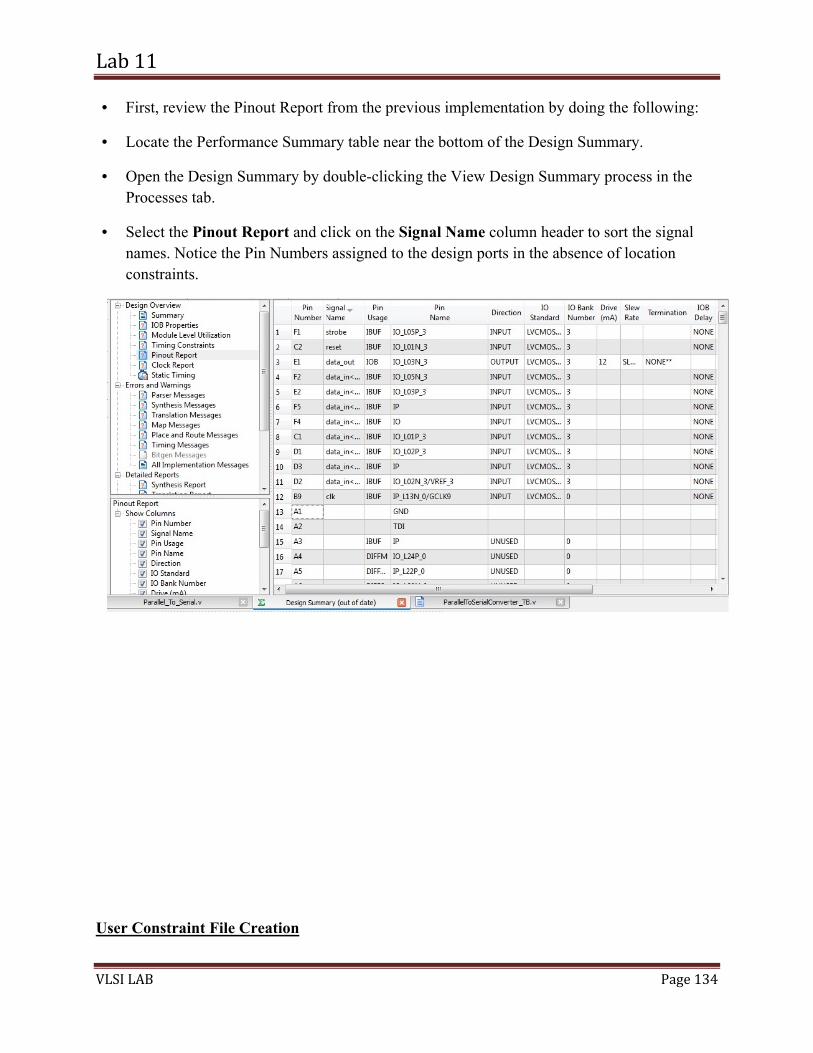
Lab 11
VLSI LAB Page 134
• First, review the Pinout Report from the previous implementation by doing the following:
• Locate the Performance Summary table near the bottom of the Design Summary.
• Open the Design Summary by double-clicking the View Design Summary process in the Processes tab.
• Select the Pinout Report and click on the Signal Name column header to sort the signal names. Notice the Pin Numbers assigned to the design ports in the absence of location constraints.
User Constraint File Creation

Lab 11
VLSI LAB Page 135
• Specify the pin locations for the ports of the design so that they are connected correctly on the Spartan 3E/ Virtex development kits.
• To constrain the design ports to package pins, do the following:
– Verify that Parallel_To_Serial is selected in the Source window.
– Create a new source by selecting Project → New Source.
– In the New Source Wizard, select Implementation Constraints File as the source type, and type ParallelToSerial_UCF in the File Name field.
– Click Next.

Lab 11
VLSI LAB Page 136
16. Assigning Pin Location
Write the following constraints in UCF file;
//Clock constraints
NET "clk" LOC = "AG18"; # Bank = 4, Pin name = IO_L6P_GC_4, Type = GCLK, Sch name = GCLK0
//Reset and Strobe Pins
NET "reset" LOC = "J19"; # Bank = 3, Pin name = IO_L3N_GC_3, Sch name = SW0
NET "strobe" LOC = "L18"; # Bank = 3, Pin name = IO_L1N_CC_GC_3, Sch name = SW1
//Datain pins
NET "data_in[0]" LOC = "K18"; # Bank = 3, Pin name = IO_L3P_GC_3, Sch name = SW2
NET "data_in[1]" LOC = "H18"; # Bank = 3, Pin name = IO_L0N_CC_GC_3, Sch name = SW3
NET "data_in[2]" LOC = "H17"; # Bank = 3, Pin name = IO_L0P_CC_GC_3, Sch name = SW4
NET "data_in[3]" LOC = "K17"; # Bank = 3, Pin name = IO_L1P_CC_GC_3, Sch name = SW5
//Dataout pins
NET "data_out" LOC = "AG8"; # Bank = 22, Pin name = IO_L18P_22, Sch name = LD0

Lab 11
VLSI LAB Page 137
• Select File → Save.
• Notice that, the Implementation processes have a orange check mark with “?” sign next to them indicating that it is required to run this process again.
Final UCF
Re-Implement Design Process

Lab 11
VLSI LAB Page 138
• Re-implement the design and verify that the ports of the Parallel_To_Serial design are routed to the package pins specifcied in the UCF.
• Re-implement the design by double-clicking the Implement Design process.
• Select the Pinout Report again and select the Signal Name column header to sort the signal names.
• Verify that signals are now being routed to the correct package pins.
• Close the Design Summary.

Lab 11
VLSI LAB Page 139
Generate Bit File
• Select Implementation in the top menu of Sources window.
• Select Parallel_To_Serial in the Sources window.
• In the Processes window, double click the Generate Programming File processes to create the bit stream of the design.

Lab 11
VLSI LAB Page 140
Download Design to FPGA Board
• This is the last step in the design verification process. This section provides simple instructions for downloading the Parallel_To_Serial design to the Spartan 3E Development board.
• Connect the 5V DC power cable to the power input on the demo board.
• Connect the download JTAG cable between the PC and demo board.
Start iMPACT Tool

Lab 11
VLSI LAB Page 141
Run Boundry Scan
Initialize JTAG Chain

Lab 11
VLSI LAB Page 142
Assign Configuration File
Assign New Configuration File
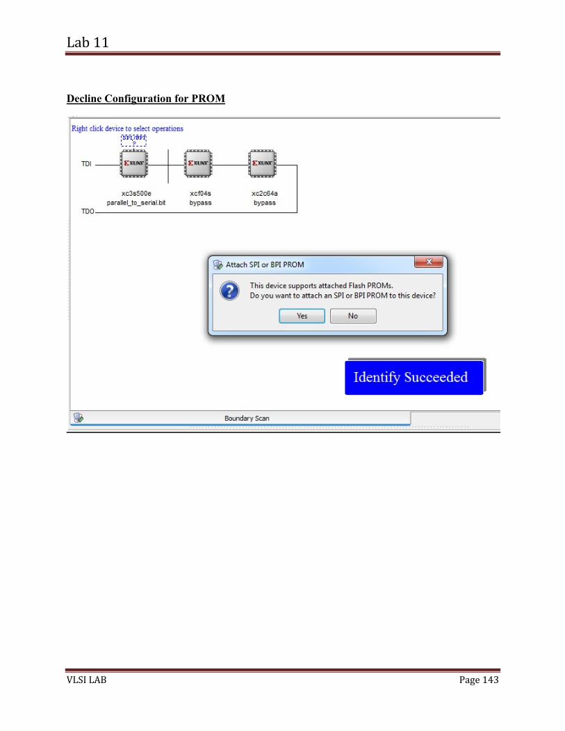
Lab 11
VLSI LAB Page 143
Decline Configuration for PROM
Lab 11
VLSI LAB Page 144
Bypass Configuration for System ACE

Lab 11
VLSI LAB Page 145
Bypass Configuration for PROM

Lab 11
VLSI LAB Page 146
Apply Device Setting Properties
Right Click on FPGA and Click at Program

Lab 11
VLSI LAB Page 147
Downloading of Design on FPGA
Download Completion
Lab 11
VLSI LAB Page 148
• The Xilinx WebTalk Dialog box may open during this process. Click Decline.
• Select Disable the collection of device usage statistics for this project only and click OK.
• iMPACT opens and the Configure Devices dialog box is displayed.
• In the Welcome dialog box, select Configure devices using Boundary-Scan (JTAG).
• Verify that Automatically connect to a cable and identify Boundary-Scan chain is selected.
• Click Finish.
• If you get a message saying that there are two devices found, click OK to continue.
• The devices connected to the JTAG chain on the board will be detected and displayed in the iMPACT window.
• The Assign New Configuration File dialog box appears. To assign a configuration file to the XC3S500E device in the JTAG chain, select the Parallel_To_Serial.bit file and click Open.
• If you get a Warning message, click OK.
• Select Bypass to skip any remaining devices.
• Right-click on the XC3S500E device image, and select Program... The Programming Properties dialog box opens.
• Click OK to program the device.
• When programming is complete, the Program Succeeded message is displayed.
• Close iMPACT without saving.

Lab 11
VLSI LAB Page 149
LAB ASSIGNMENTS Lab Assignment: Write UCF file for 4-bit Ripple Carry Counter which we design in Lab 7.
OBSERVATION & RESULT: __________________________________________________________________
__________________________________________________________________
__________________________________________________________________
__________________________________________________________________
__________________________________________________________________