Virtex Series Configuration Architecture User Guide · The bitstream is a series of configuration...
45
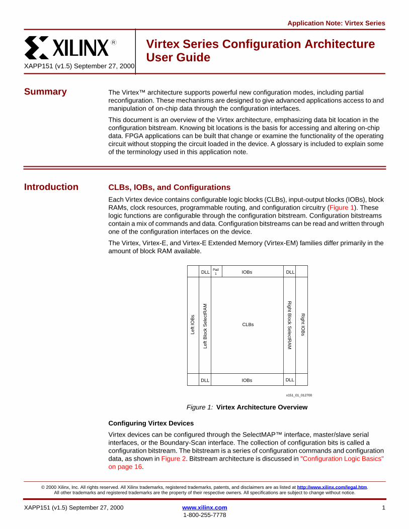
XAPP151 (v1.5) September 27, 2000 www .xilinx.com 1 1-800-255-7778 © 2000 Xilinx, Inc. All rights reserved. All Xilinx trademarks, registered trademarks, patents, and disclaimers are as listed at http://www .xilinx.com/legal.htm. All other trademarks and registered trademarks are the property of their respective owners. All specifications are subject to change without notice. Summary The Virtex™ architecture supports powerful new configuration modes, including partial reconfiguration. These mechanisms are designed to give advanced applications access to and manipulation of on-chip data through the configuration interfaces. This document is an overview of the Virtex architecture, emphasizing data bit location in the configuration bitstream. Knowing bit locations is the basis for accessing and altering on-chip data. FPGA applications can be built that change or examine the functionality of the operating circuit without stopping the circuit loaded in the device. A glossary is included to explain some of the terminology used in this application note. Introduction CLBs, IOBs, and Configurations Each Virtex device contains configurable logic blocks (CLBs), input-output blocks (IOBs), block RAMs, clock resources, programmable routing, and configuration circuitry (Figure 1). These logic functions are configurable through the configuration bitstream. Configuration bitstreams contain a mix of commands and data. Configuration bitstreams can be read and written through one of the configuration interfaces on the device. The Virtex, Virtex-E, and Virtex-E Extended Memory (Virtex-EM) families differ primarily in the amount of block RAM available. Configuring Virtex Devices Virtex devices can be configured through the SelectMAP™ interface, master/slave serial interfaces, or the Boundary-Scan interface. The collection of configuration bits is called a configuration bitstream. The bitstream is a series of configuration commands and configuration data, as shown in Figure 2. Bitstream architecture is discussed in "Configuration Logic Basics" on page 16. Application Note: Virtex Series XAPP151 (v1.5) September 27, 2000 Virtex Series Configuration Architecture User Guide R Figure 1: Virtex Architecture Overview DLL DLL DLL DLL IOBs IOBs Pad 1 Right IOBs Right Block SelectRAM Left IOBs Left Block SelectRAM x151_01_012700 CLBs
Transcript of Virtex Series Configuration Architecture User Guide · The bitstream is a series of configuration...
Summary The Virtextrade architecture supports powerful new configuration modes including partialreconfiguration These mechanisms are designed to give advanced applications access to andmanipulation of on-chip data through the configuration interfaces
This document is an overview of the Virtex architecture emphasizing data bit location in theconfiguration bitstream Knowing bit locations is the basis for accessing and altering on-chipdata FPGA applications can be built that change or examine the functionality of the operatingcircuit without stopping the circuit loaded in the device A glossary is included to explain someof the terminology used in this application note
Introduction CLBs IOBs and ConfigurationsEach Virtex device contains configurable logic blocks (CLBs) input-output blocks (IOBs) blockRAMs clock resources programmable routing and configuration circuitry (Figure 1) Theselogic functions are configurable through the configuration bitstream Configuration bitstreamscontain a mix of commands and data Configuration bitstreams can be read and written throughone of the configuration interfaces on the device
The Virtex Virtex-E and Virtex-E Extended Memory (Virtex-EM) families differ primarily in theamount of block RAM available
Configuring Virtex Devices
Virtex devices can be configured through the SelectMAPtrade interface masterslave serialinterfaces or the Boundary-Scan interface The collection of configuration bits is called aconfiguration bitstream The bitstream is a series of configuration commands and configurationdata as shown in Figure 2 Bitstream architecture is discussed in Configuration Logic Basicson page 16
Application Note Virtex Series
XAPP151 (v15) September 27 2000
Virtex Series Configuration ArchitectureUser Guide
R13
Figure 1 Virtex Architecture Overview
DLL
DLL DLL
DLL
IOBs
IOBsPad13
1
Right IO
Bs
Right B
lock SelectR
AM
Left
IOB
s
Left
Blo
ck S
elec
tRA
M
x151_01_012700
CLBs
XAPP151 (v15) September 27 2000 wwwxilinxcom 11-800-255-7778
copy 2000 Xilinx Inc All rights reserved All Xilinx trademarks registered trademarks patents and disclaimers are as listed at httpwww xilinxcomlegalhtm All other trademarks and registered trademarks are the property of their respective owners All specifications are subject to change without notice
Virtex Series Configuration Architecture User GuideR13
Writing some or all of a configuration is done by issuing configuration commands to the desiredinterface followed by the configuration data
The SelectMAP interface is an 8-bit interface on the device with data pins labeled D[70] Theconfiguration bitstream can be written eight bits per clock cycle Virtex devices can beconfigured to retain the (D[70] BUSYDOUT INIT WRITE and CS) SelectMAP pins allowingfurther re-configuration via those pins If further re-configuration is not required those pins canbe configured as user IO
When the masterslave serial or Boundary Scan interface is used for configuration or re-onfiguration the configuration bitstream is transmitted one bit per clock cycle
Timing relationships for the configuration interfaces are discussed in the Virtex series datasheets located at httpwww xilinxcompr oductsvir texhtm
Reading Configuration Bits From a Virtex Device
Configuration data can be read using the SelectMAP interface or the Boundary Scan interfaceThe masterslave serial interfaces can not be used to read a configuration Reading all or someof a configuration is done by issuing configuration read commands to the desired interfacethen reading the data from the same interface Configuration commands and data formats arediscussed in Configuration Logic Basics on page 16
The SelectMAP interface has an 8-bit data port To use the SelectMAP interface afterconfiguration all 12 SelectMAP pins must remain as SelectMAP as opposed to user IO (usingthe BitGen option -g PersistYes )
The Boundary Scan (JTAG) interface allows bit-serial access to the configuration It is apermanent interface that is always present
ConfigurationColumns
The Virtex configuration memory can be visualized as a rectangular array of bits The bits aregrouped into vertical frames that are one-bit wide and extend from the top of the array to thebottom A frame is the atomic unit of configuration - it is the smallest portion of the configurationmemory that can be written to or read from
Frames are grouped together into larger units called columns In Virtex Virtex-E andVirtex-EM devices there are several different types of columns
CMD 1 data CMD 2 data CMD 3 data CMD 1
Figure 2 Bitstream Example
Warning This document discusses mechanisms for manipulating the configuration bits for theVirtex devices If portions of the bitstream other than those described here are altered thedevice may be damaged Xilinx is not liable for any consequences of misprogramming adevice
2 wwwxilinxcom XAPP151 (v15) September 27 20001-800-255-7778
Virtex Series Configuration Architecture User GuideR13
Each device contains one center column that includes configuration for the four global clockpins Two IOB columns represent configuration for all of the IOBs on the left and right edges ofthe device The majority of columns are CLB columns which each contain one column of CLBsand the two IOBs above and below those CLBs The remaining two column types involve theblock RAM one for content and the other for interconnect For each RAM column one of eachtype is present (for values for all Virtex devices see Table 3 ldquoVirtex Series Devicesrdquo onpage 6)
The columns for an sample Virtex device are shown below
ConfigurationAddressing
Block Type Major Address Minor AddressThe total address space is divided into block types There are two block types RAM and CLBThe RAM type contains only the block SelectRAM content columns (not interconnect) TheCLB type contains all other column types
Both the RAM and CLB address spaces are subdivided into major and minor addresses Eachconfiguration column has a unique major address within the RAM or CLB space Eachconfiguration frame has a unique minor address within its column
The numbering schemes for the block type and minor address are identical between VirtexVirtex-E and Virtex-EM devices The major address numbering scheme differs betweenfamilies and is encapsulated in Table 2 But in both families even major addresses are on theleft half of the device while the odd major addresses are on the right half of the device
Table 1 Configuration Column Type
Column Type of
Frames per Device
Center 8 1
CLB 48 of CLB columns
IOB 54 2
Block SelectRAM Interconnect 27 of Block SelectRAM columns
Block SelectRAM Content 64 of Block SelectRAM columns
2IOB
s
2IOB
s
2GCL
K
2IOB
s
2IOB
s
Left
IOB
Col
umn
(54
fram
es)
Blo
ck S
elec
tRA
MC
onte
nt (
64 fr
ames
)
Blo
ck S
elec
tRA
MIn
terc
onne
ct (
27 fr
ames
)
CLB
Col
umn
(48
fram
es)
hellip
CLB
Col
umn
(48
fram
es)
Cen
ter
Col
umn
(8 fr
ames
)
CLB
Col
umn
(48
fram
es)
hellip
CLB
Col
umn
(48
fram
es)
Blo
ck S
elec
tRA
MIn
terc
onne
ct(2
7 fr
ames
)
Blo
ck S
elec
tRA
MC
onte
nt (
64 fr
ames
)
Rig
ht IO
B C
olum
n(5
4 fr
ames
)
2IOB
s
2IOB
s
2GCL
K
2IOB
s
2IOB
s
Figure 3 Configuration Column Example (XCV50)
XAPP151 (v15) September 27 2000 wwwxilinxcom 31-800-255-7778
Virtex Series Configuration Architecture User GuideR13
Virtex Major Addresses
The CLB address space begins with rsquo0rsquo for the center column and alternates between the rightand left halves of the device for all the CLB columns then IOB columns and finally blockSelectRAM interconnect columns
The RAM address space has lsquo0rsquo for the left block SelectRAM content column and lsquo1rsquo for theright column
A XCV50 is shown in Figure 4 The shaded columns are in the RAM address space
Virtex-EM Major Addresses
The Virtex-EM family has the same numbering as the Virtex family but the block SelectRAMcontent columns begin with 1
Virtex-E Major Addresses
The Virtex-E family has block SelectRAM interspersed between CLB columns Both the CLBand RAM major addressing have been changed to allow for this
The CLB address space again begins with lsquo0rsquo for the center column and alternates between theright and left sides of the device for CLB columns and block SelectRAM interconnect columnsand finally IOB columns The difference is that in Virtex-E devices the block SelectRAM
Table 2 Major Addressing Scheme by Family
Column Type Block Type Virtex Virtex-E Virtex-EM
First MJA CLB 0 0 0
RAM 0 1 1
MJA Order CLB 1 Center2 CLB3 IOB4 BRAM Interconnect
1 Center2 CLB BRAM Interconnect3 IOB
1 Center2 CLB3 IOB4 BRAM Interconnect
RAM BRAM Content BRAM Content BRAM Content
2IOBs
2IOBs
2GCL
K
2IOBs
2IOBs
Left
IOB
Col
umn
(54
fram
es)
Blo
ck S
elec
tRA
MC
onte
nt (
64 fr
ames
)
Blo
ck S
elec
tRA
MIn
terc
onne
ct (
27 fr
ames
)
CLB
Col
umn
(48
fram
es)
hellip
CLB
Col
umn
(48
fram
es)
Cen
ter
Col
umn
(8 fr
ames
)
CLB
Col
umn
(48
fram
es)
hellip
CLB
Col
umn
(48
fram
es)
Blo
ck S
elec
tRA
MIn
terc
onne
ct (
27 fr
ames
)B
lock
Sel
ectR
AM
Con
tent
(64
fram
es
Rig
ht IO
B C
olum
n(5
4 fr
ames
)
2IOBs
2IOBs
2GCL
K
2IOBs
2IOBs
IOLe
ft
RA
M0
BIC
0
C1
C12
Cen
ter
C13
C24
BIC
1
RA
M1
IOR
ight
MA 26 0 28 24 2 0 1 23 27 1 25
Figure 4 Virtex Family Allocation of Frames to Device Resources (XCV50)
4 wwwxilinxcom XAPP151 (v15) September 27 20001-800-255-7778
Virtex Series Configuration Architecture User GuideR13
interconnect appear in the middle of the CLB addresses while in the Virtex and Virtex-EMfamilies they appear at the very end after the IOB columns Also note that the blockSelectRAM content columns begin with lsquo1rsquo (Virtex devices begin with lsquo0rsquo)
A XCV50E is shown in Figure 5 The shaded columns are in the RAM address space
Frames Frames are read and written sequentially with ascending addresses for each operationMultiple consecutive frames can be read or written with a single configuration command Thesmallest amount of data that can be read or written with a single command is a single frameThe entire CLB array plus the IOBs and block SelectRAM interconnect can be read or writtenwith a single command Each block SelectRAM Content must be read or written separately
Frame SizesFrame size depends on the number of rows in the device The number of configuration bits ina frame is 18 times ( CLB_rows+2) and is padded with zeroes on the right (bottom) to fit in 32-bitwords See Frame Organization on page 6 An additional padding word is needed at the endof each frame for pipelining Table 3 shows the frame sizes for all Virtex devices This table alsoshows the size in words of the bitstream for the CLB address space and the number of wordsin each RAM block
2IOB
s
2IOB
s
2IOB
s
2IOB
s
2GCLK
2IOB
s
2IOB
s
Blo
ck S
elec
tRA
MIn
terc
on
ne
ct(2
7 f
ram
es)
2IOB
s
2IOB
s
Blo
ck S
elec
tRA
MC
onte
nt (
64 fr
ames
)
Left
IOB
Col
umn
(54
fram
es)
Blo
ck S
elec
tRA
MC
onte
nt (
64 fr
ames
)B
lock
Sel
ectR
AM
Inte
rco
nn
ect(2
7 f
ram
es)
CLB
Col
umn
(48
fram
es)
hellipC
LB C
olum
n(4
8 fr
ames
)B
lock
Sel
ectR
AM
Con
tent
(64
fram
es)
Blo
ck S
elec
tRA
MIn
terc
on
ne
ct(2
7 f
ram
es)
CLB
Col
umn
(48
fram
es)
hellip
CLB
Col
umn
(48
fram
es)
Cen
ter
Col
umn
(8 fr
ames
)C
LB C
olum
n(4
8 fr
ames
)
hellip
CLB
Col
umn
(48
fram
es)
Blo
ck S
elec
tRA
MC
onte
nt (
64 fr
ames
)C
LB C
olum
n(4
8 fr
ames
)
hellip
CLB
Col
umn
(48
fram
es)
Blo
ck S
elec
tRA
MIn
terc
on
ne
ct(2
7 f
ram
es)
Rig
ht IO
B C
olum
n(5
4 fr
ames
)
2IOB
s
2IOB
s
2IOB
s
2IOB
s
2GCLK
2IOB
s
2IOB
s
2IOB
s
2IOB
s
IOLe
ft
RA
M0
BIC
0
C1
C6
RA
M1
BIC
1
C7
C12
Cen
ter
C13
CLB
18
BIC
2
RA
M2
C19
C24
BIC
3
RA
M3
IOR
ight
MA
30 4 28 26 16 2 14 12 2 0 1 11 13 1 15 25 27 3 29
Figure 5 Virtex-E Family Allocation of Frames to Device Resources (XCV50E)
XAPP151 (v15) September 27 2000 wwwxilinxcom 51-800-255-7778
Virtex Series Configuration Architecture User GuideR13
Frame OrganizationEach frame sits vertically in the device with the ldquofrontrdquo of the frame at the top As shown inFigure 6 it is convenient to consider the frame horizontally when it is viewed as part of abitstream The top IOBs are shown on the left followed by the CLBs in the column and thebottom IOBs on the right Bits in frames are allocated as follows
For CLB columns the first 18 bits control the two IOBs at the top of the column then 18 bits areallocated for each CLB row finally the next 18 bits control the two IOBs at the bottom of the
Table 3 Virtex Series Devices
Device Row times ColBits
FrameWordsFrame
Virtex Virtex-E
RAMCols
of 32-bit Read-backWords (1)
RAMCols
RAMSpace
of 32-bit Read-backWords (1)
CLB(all)
RAM(1 col)
CLB(all)
RAM(1 col)
XCV50 16 times 24 384 12 2 15876 780 - - - -
XCV50E 16 times 24 384 12 - - - 4 6 16524 780
XCV100 20 times 30 448 14 2 22554 910 - - - -
XCV100E 20 times 30 448 14 - - - 4 12 23310 910
XCV150 24 times 36 512 16 2 30384 1040 - - - -
XCV200 28 times 42 576 18 2 39366 1170 - - - -
XCV200E 28 times 42 576 18 - - - 4 12 40338 1170
XCV300 32 times 48 672 21 2 51975 1365 - - - -
XCV300E 32 times 48 672 21 - - - 4 12 53109 1365
XCV400 40 times 60 800 25 2 76275 1625 - - - -
XCV400E 40 times 60 800 25 - - - 4 12 77625 1625
XCV405E 40 times 60 800 25 - - - 14 4 84375 1625
XCV600 48 times 72 960 30 2 108810 1950 - - - -
XCV600E 48 times 72 960 30 - - - 6 12 112050 1950
XCV800 56 times 84 1088 34 2 142902 2210 - - - -
XCV812E 56 times 84 1088 34 - - - 20 4 159426 2210
XCV1000 64 times 96 1248 39 2 186381 2535 - - - -
XCV1000E 64 times 96 1248 39 - - - 6 12 190593 2535
XCV1600E 72 times 108 1376 43 - - - 8 12 237231 2795
XCV2000E 80 times 120 1536 48 - - - 8 12 292464 3120
XCV2600E 92 times 138 1728 54 - - - 8 12 375678 3510
XCV3200E 104 times 156 1952 61 - - - 8 12 477081 3965
Notes1 Includes pad frame in calculation
6 wwwxilinxcom XAPP151 (v15) September 27 20001-800-255-7778
Virtex Series Configuration Architecture User GuideR13
CLB column The frame then contains enough ldquopadrdquo bits to make it an integral multiple of 32bits
For IOB columns the frame allocates 18 bits per three IOB rows Figure 7 When reading andwriting frames bits are grouped into 32-bit words starting on the left (corresponding to the topof the device) If the last word does not completely fill a 32-bit word it is padded on the right withzeroes
For block SelectRAM content columns (Figure 8) the first 18 bits are pad bits then 72 bits areallocated for each RAM row finally there are another 18 pad bits The frame then adds enoughldquopadrdquo bits to make it an integral multiple of 32 bits
Location of LUT SelectRAM BitsWith respect to the beginning of a configuration frame relative locations of LUT SelectRAM bitswithin the bitstream are the same for every CLB slice The bits of a LUT SelectRAM are spreadacross 16 consecutive frame Minor Addresses Each frame Minor Address contains allinstances of a single bit index for that column These 16 frames contain all 16 bits of the LUTSelectRAM for a column of CLB slices You must read or write the 16 frames containing thosebits to read or write the entire LUT SelectRAM
Figure 6 CLB Column Frame Organization
Figure 7 IOB Column Frame Organization
Figure 8 Block SelectRAM Content Column Frame Organization
Note LUT SelectRAM bits are stored inverted Flip-Flop data are stored in their true senseWhen reading or writing LUT SelectRAM data from the bitstream it is negated from the logicsense of the data For example a 4-input AND gate has the truth tableLUT[150] = 1000000000000000
This truth table isstored internally in theLUTSelectRAMasLUT[150] = 0111111111111111Ofcourse user logic reading the data from the LUT SelectRAM would read the correct logicvalue LUT[150] = 1000000000000000
Top 2 IOBs13 Bottom 2 IOBs1313
CLB Rn1313
13 18131813181318131813
CLB R213CLB R113
x151_06_020700
Top 3 IOBs Bottom 3 IOBs1313
181818
3 IOBs
x151_07_020800
Pad PadRAM Rn
1872727218
RAM R1RAM R0
x151_08_021800
XAPP151 (v15) September 27 2000 wwwxilinxcom 71-800-255-7778
Virtex Series Configuration Architecture User GuideR13
ConfigurationData Operations
Reading Configuration DataConfiguration information can be read from the Virtex devices if readback is enabled in thecurrent configuration (See the description of the Control Register field SBITS on page 21)CLB and IOB configuration data can be read while the device is operating
When reading data from a Virtex device a pad frame is read before any of the data framesThis is in addition to the pad word in each data frame The pad frame must be included in theword count to be read from the device
Each frame read from the device consists of the number of words shown in Table 3
For example the XCV150 has 16-word frames When reading frames the first word of a frameis a pad word Including the pad frame the XCV150 has 1899 (3038416) frames (SeeFigure 9)
Writing Configuration DataConfiguration information can be written to a Virtex device while the device is running if writingis enabled in the current configuration (See the Control Register field SBITS in Table 23) Re-writing the same configuration data does not generate any transient signals
Changing configuration data may generate transient signals especially if LUT values or signalrouting is changed For this case all the logic cells and routing can be placed in a non-contentious state by asserting the GHIGH_B signal See the description for the CommandRegister (CMD) on page 18
When writing configuration data to the Virtex device whether from the SelectMAP or JTAGinterfaces the data frames are written to the device with each frame followed by a pad wordAfter all the data frames are written a pad frame must be written (to flush internal pipelines)The pad words and pad frame must be included in the number of words to be written to thedevice (Table 3)
For example the XCV1000 has 39-word frames When writing frames the last word of theframe is a pad word Including the pad frame the XCV1000 has 4779 (18638139) framesSee Figure 10)
Altering Configuration DataVirtex devices support the Read-Modify-Write (RMW) method of changing LUT SelectRAMdata Therefore it is possible to read or alter the contents of one or more LUT SelectRAMsthrough the JTAG or SelectMAP interfaces When writing data to one or more LUTSelectRAMs all the bits in the frame must have valid configuration information This can beassured by altering valid configurations from bitstream files or from frames read from a properlyconfigured Virtex device When using the RMW method it may be expeditious to read the dataignoring the pad frame and the pad word of only the first frame This aligns the remaining
Pad Frame (16 words)Pad Word Data Frame 0 (15 words)
hellip
hellip
Pad Word Data Frame n (15 words)
Figure 9 XCV150 Frame Padding for Device Read
Data Frame 0 (38 words) Pad Word
hellip
Data Frame n (38 words) Pad WordPad Frame (39 words)
Figure 10 XCV1000 Frame Padding for Device Write
8 wwwxilinxcom XAPP151 (v15) September 27 20001-800-255-7778
Virtex Series Configuration Architecture User GuideR13
configuration data in the Device Write format After modifying the configuration the altered datacan be written to the Virtex device followed by a pad word and a pad frame
It is not necessary to retain the contents of the pad frame or pad words However pad wordsand pad frames are included in the CRC calculation
Definitions Two sets of variables are defined to determine where a desired bit is in the configuration dataThe first is a set of ldquoindependentrdquo variables or design attributes namely characteristics of thedesign that are known ie the device size and which CLB and bit(s) within the CLB to locateTable 4 The second set is a set of ldquodependentrdquo variables or design variables namely valuesthat must be calculated to find the bit(s) of interest listed in Table 5
Note Frames span an entire column of CLB slices (or IOBs) Thus when changing LUTSelectRAM bit 0 for a single CLB slice (eg R3C4S1) LUT SelectRAM bit 0 for all slices inthat column (ie RC4S1) is written with the same command One must ensure that either allother data in the slice is constant or changed externally through partial configurations
LUT SelectRAMs not configured externally should not lie in the same slice with LUTs or LUTSelectRAMs that are re-configured externally Such a mixture can cause the unrelated LUTSelectRAM data to be re-configured when the frames are written to the device Figure 11shows what can happen if this restriction is not observed
In this example it is the objective to perform a Read-Modify-Write on the LUT SelectRAM inR2C3S1 in column 3 which is shown in the first column in the figure Row 2 contains a LUTcontaining the value AB Row 3 contains a SelectRAM containing the value C3 Because theRead and Write operations operate on an entire frame the RAM in R3C3S1 is also read andwritten when R2C3S1 is read and written Performing the Readback operation reads all theLUT and SelectRAM values for the column Before the new value for the LUT is written it ispossible for the on-chip circuitry to write a new value such as 14 into the SelectRAM Whenthe new value BD is written via the configuration interface into LUT R2C3S1 the value C3 isalso written into RAM R3C3S1 This may not always be desirable (It is design-dependent)
Figure 11 Potential Write Conflicts
x151_11_020800
LUT R2C3S113AB13
RAM R3C3S113C313
Before13Readback
13
LUT R2C3S113AB13
RAM R3C3S1131413
Before13Configuration 13
Write
13
LUT R2C3S113BD13
RAM R3C3S113C313
After13Configuration13
Write
13
Table 4 Design Attributes (Independent Variables)
Term Definition
Chip_Cols of CLB columns on the Virtex device
Chip_Rows of CLB rows on the Virtex device
Chip_Rams of block SelectRAM columns on the Virtex device
RAM_Space Spacing of block SelectRAM columns (in terms of CLB columns)
FL of 32-bit words in the frame
XAPP151 (v15) September 27 2000 wwwxilinxcom 91-800-255-7778
Virtex Series Configuration Architecture User GuideR13
RW 1 for Read 0 for Write
CLB_Col Column number of the desired CLB
CLB_Row Row number of the desired CLB
Slice 0 or 1
FG 0 for the F-LUT 1 for the G-LUT
lut_bit The desired bit from the given LUT Bits in the LUT are indexed from 0 to 15
XY 0 for the X Flip-Flop 1 for the Y Flip-Flop
RAM_Col Column number of the desired block SelectRAM
RAM_Row Row number of the desired block SelectRAM
ram_bit The desired bit from the given block SelectRAM Bits are indexed from 0 to4095
Table 5 Design Variables (Dependent Variables)
Term Definition
MJA Frame Major Address
MNA Frame Minor Address
fm_st_wd The index of the word within a full configuration segment that correspondsto the starting word of the desired frame A full configuration segment isdefined as the following 1) for CLBIOB all CLB IOB and RAMinterconnect frames beginning at MJA=0 MNA=0 and 2) for blockSelectRAM all RAM content frames for the given RAM column Words arenumbered starting at 0
fm_wd The index of the 32-bit word within a frame that contains the desired bitWords in a frame are numbered starting at 0
fm_wd_bit_idx The bit index of the desired bit within frame word fm_wd Words areindexed in ldquobig-endianrdquo style with bit 31 on the left and bit 0 on the right
fm_bit_idx Bit index within a frame of the desired bit Numbered starting with 0 as theleft-most (first) bit Bit numbering within a frame continues across all thewords in the frame
Table 6 Functions used in Equations
Functions Definition
floor(x) The largest integer not larger than x Eg floor(31) = 3 because the nextlargest integer 4 is larger than 31 floor(3)=3
ceiling(x) The smallest integer greater than or equal to x For example ceiling(32) = 4because 4 is greater than 32 and 3 is not ceiling (4) = 4
The modulus operation 5 2 = 1 5 3 = 2 5 5 = 0
Table 4 Design Attributes (Independent Variables) (Continued)
Term Definition
10 wwwxilinxcom XAPP151 (v15) September 27 20001-800-255-7778
Virtex Series Configuration Architecture User GuideR13
CLB LUTSelectRAMDependentVariables
Table 7 shows equations for the LUT SelectRAM ldquoDependent Variablesrdquo that were defined inTable 5
Virtex-E CLB LUT SelectRAM Dependent VariablesThe additional block SelectRAM columns in Virtex-E devices require an adjustment to the MJAThe following equations calculate the adjustment necessary for each of the affected dependentvariables For each variable calculate the base value based upon the Virtex equations onlyand then add the resulting Virtex adjustment
The left and right sides of the device are treated differently
LUT SelectRAM ExamplesSee ldquoExamplesrdquo on page 27 for several examples of reading and evaluating configuration dataThe examples illustrate how to make use of these equations to find the desired data in abitstream
Table 7 Virtex Equations for LUT SelectRAM Dependent Variables
Term Definition
MJA if (CLB_Col le Chip_Cols2)then Chip_Cols ndash CLB_Col times 2 + 2else 2 times CLB_Col ndash Chip_Cols ndash 1
MNA lut_bit + 32 ndash Slice times (2 times lut_bit + 17)
fm_bit_idx 3 + 18 times CLB_Row ndash FG + RW times 32
fm_st_wd FL times (8 + (MJA ndash1) times 48 + MNA) + RW times FL
fm_wd floor(fm_bit_idx32)
fm_wd_bit_idx 31 + 32 times fm_wd ndash fm_bit_idx
Notes
bull Do NOT input the final results back into the original Virtex equations (eg do not useMJAfinal value to calculate fm_st_wd)
bull MJAfinal = MJA + MJA_adj
bull fm_st_wdfinal = fm_st_wd + fm_st_wd_adj
Table 8 CLB Location
CLB Location CLB Column
Left CLB_Col le Chip_Cols2
Right CLB_Col gt Chip_Cols2
Table 9 Virtex-E Families Adjustments for LUT SelectRAM Dependent Variables
Term Definition
MJA_adj Left RAM_Bound = (Chip_Rams2 - 1) x RAM_SpaceMJA_adj = 2 x ceiling((RAM_Bound - CLB_Col + 1) RAM_Space)
Right
RAM_Bound = Chip_Cols - (Chip_Rams2 - 1) x RAM_Space + 1MJA_adj = 2 x ceiling((CLB_Col - RAM_Bound + 1) RAM_Space)
fm_st_wd_adj FL times (27 x MJA_adj)
XAPP151 (v15) September 27 2000 wwwxilinxcom 111-800-255-7778
Virtex Series Configuration Architecture User GuideR13
CLB Flip-FlopDependentVariables
Equations for the CLB flip-flops can be found in Table 10 Their locations are calculatedsimilarly to the LUT SelectRAM locations Equations for the CLB FF Dependent Variables aredefined in Table 5
Virtex-E CLB Flip-Flop Dependent VariablesApply the adjustments given in Table 8 and Table 9
IOB DependentVariables
Each IOB contains four values that can be captured into special registers These values are
bull I mdash the input flip-flop
bull O mdash the output flip-flop
bull T mdash the flip-flop for the tri-state control
bull P mdash the value of the IO pad
These values are captured by utilizing the CAPTURE_VIRTEX symbol in your design TheLibraries Guide has more details on the use of this symbol The following registers will be readas part of the readback data
Access to the IOB flip-flops is different for the top and bottom IOBs versus the left and rightIOBs
The top and bottom IOBs are part of the CLB column frames There are two IOBs at the top andbottom of each CLB column
The left and right IOBs are in columns by themselves There are three IOBs per CLB row
IOBs are numbered clockwise around the die Pad 1 is located at the left side of the top edgeabove CLB column 1 The equations for where to find IOB flip-flops in the bitstream are basedon the pad number which is the same for a given size device not the package pin name whichvaries from package to package The mapping from package pin names to pad numbers canbe found in EPIC or fpga_editor
Table 11 contains the numeric pad indices for the pads on all four edges of the device in termsof the number of CLB columns and rows on the device
Table 10 Virtex Equations for CLB FF Dependent Variables
Term Definition
MJA if (CLB_Col le Chip_Cols2)then Chip_Cols ndash CLB_Col times 2 + 2else 2 times CLB_Col ndash Chip_Cols ndash 1
MNA Slice times (12 times XY ndash 43) ndash 6 times XY + 45
fm_bit_idx (18 times CLB_Row) + 1 + (32 times RW)
fm_st_wd FL times (8 + (MJA ndash1) times 48 + MNA) + RW times FL
fm_wd floor(fm_bit_idx32)
fm_wd_bit_idx 31 + 32 times fm_wd ndash fm_bit_idx
12 wwwxilinxcom XAPP151 (v15) September 27 20001-800-255-7778
Virtex Series Configuration Architecture User GuideR13
Table 12 shows the equations for the dependent variables for the IOB flip-flops The variable iin this table refers to the index of pad i
Table 11 IOB Pad Indices
PadLocation Pad Index i
Top 1 le i le Chip_Cols times 2
Right Chip_Cols times 2 +1 le i le Chip_Cols times 2 + Chip_Rows times 3
Bottom Chip_Cols times 2 + Chip_Rows times 3 + 1 le i le Chip_Cols times 4 + Chip_Rows times 3
Left Chip_Cols times 4 + Chip_Rows times 3 + 1 le i le Chip_Cols times 4 + Chip_Rows times 6
Table 12 Equations for IOB Dependent Variables
Term Definition
MJA
Topif (i le Chip_Cols)then Chip_Cols ndash ceiling(i2) times 2 + 2else 2 times ceiling (i2) ndash Chip_Cols ndash1
Right Chip_Cols + 1
Bottomif (i gt 3 times (Chip_Cols + Chip_Rows))then 2 times ceiling((i ndash 3 times Chip_Cols ndash 3 times Chip_Rows)2)else Chip_Cols ndash 2 times floor((i ndash 2 times Chip_Cols ndash 3 times Chip_Rows ndash 1)2) ndash 1
Left Chip_Cols + 2
MNA
Top
I ndash 25 times (i2) + 45
O ndash 13 times (i2) + 39
T ndash 5 times (i2) + 35
P ndash 4 times (i2) + 25
Right
I t = (i ndash 2 times Chip_Cols) 3 MNA = 275 times t2 ndash 575 times t + 32
O t = (i ndash 2 times Chip_Cols) 3 MNA = 215 times t2 ndash 515 times t + 38
T t = (i ndash 2 times Chip_Cols) 3 MNA = 175 times t2 ndash 475 times t + 42
P 50
Bottom
I 25 times ((i ndash 2 x Chip_Cols - 3 x Chip_Rows)2) + 20
O 13 times ((i ndash 2 x Chip_Cols - 3 x Chip_Rows)2) + 26
T 5 times ((i ndash 2 x Chip_Cols - 3 x Chip_Rows)2) + 30
P 4 times ((i ndash 2 x Chip_Cols - 3 x Chip_Rows)2) + 21
Left
I t = (i ndash 4 x Chip_Cols - 3 x Chip_Rows)3 MNA = 175 times t2 ndash 475 times t + 45
O t = (i ndash 4 x Chip_Cols - 3 x Chip_Rows)3 MNA = 235 times t2 ndash 535 times t + 39
T t = (i ndash 4 x Chip_Cols - 3 x Chip_Rows)3 MNA = 275 times t2 ndash 575 times t + 35
P 50
XAPP151 (v15) September 27 2000 wwwxilinxcom 131-800-255-7778
Virtex Series Configuration Architecture User GuideR13
Virtex-E IOB Dependent VariablesSimilar to CLB dependent variables only the variables affected by the major address aredifferent in Virtex-E and Virtex-EM devices versus Virtex devices A simple way to account forthe change is to determine the CLB column where the pad resides (only true for top andbottom) Then the adjustment calculated for the CLB column can be applied The conversionto CLB columns is found in Table 13
fm_bit_idx
Top 32 times RW
Right
I O ampT 18 times (1 + floor ((i ndash 2 times Chip_Cols ndash 1)3)) + 32 times RW
Pt = (i ndash 2 times Chip_Cols) 3fm_bit_idx = 18 times (1 + floor ((i ndash 2 times Chip_Cols ndash 1)3)) + 6 times t2 ndash 17 times t + 15 + 32 timesRW
Bottom 18 times (Chip_Rows + 1)+ 32 times RW
Left
I O ampT18 times (Chip_Rows ndash floor((i ndash 4 times Chip_Cols ndash 3 times Chip_Rows ndash 1)3)) + 32 times RW
Pt = (i ndash 4 times Chip_Cols ndash 3 times Chip_Rows)3fm_bit_idx = 18 times (Chip_Rows ndash floor ((i ndash 4 times Chip_Cols ndash 3 times Chip_Rows ndash 1)3))ndash 105 times t2 + 215 times t + 4 + 32 times RW
fm_st_wdif (MJA gt Chip_Cols + 1)then FL times (54 times MJA ndash 46 + MNA ndash 6 times Chip_Cols) + RW times FLelse FL times (8 + (MJA ndash1) times 48 + MNA) + RW times FL
fm_wd floor (fm_bit_idx32)
fm_wd_bit_idx 31 + 32 times fm_wd ndash fm_bit_idx
Table 12 Equations for IOB Dependent Variables (Continued)
Term Definition
Table 13 Pad -gt CLB Column
Term Definition
CLB_ColTop ceiling(i2)
Bottom ceiling((4 x Chip_Cols + 3 x Chip_Rows + 1 - i)2)
Table 14 Virtex-E Families Adjustments for IOB Dependent Variables
Term Definition
MJA_adj
Top use Table 8 and Table 9
Right Chip_Rams
Bottom use Table 8 and Table 9
Left Chip_Rams
fm_st_wd_adj FL times (27 x MJA_adj)
14 wwwxilinxcom XAPP151 (v15) September 27 20001-800-255-7778
Virtex Series Configuration Architecture User GuideR13
BlockSelectRAMDependentVariables
The equations for the block SelectRAM dependent variables are given in Table 15 Therelationship of a particular memory cell index in the context of a given configuration is describedin XAPP130 ldquoUsing the Vir tex Bloc k SelectRAM+ Resour cerdquo
Virtex-E Block SelectRAM Dependent VariablesThe RAM major address numbering scheme changed slightly such that the lowest MJA on theleft side is now 2 instead of 0 As in the case for the CLB equations the adjustments belowshould be applied after the Virtex equations
Table 15 Virtex Equations for Block SelectRAM Dependent Variables
Term Definition
MJAif (RAM_Col lt Chip_Rams2)then 2 x (Chip_Rams2 - 1 - RAM_Col)else 2 x (RAM_Col - Chip_Rams2) + 1
MNA
1 x floor(((ram_bit 64) 64)32) + 2 x floor(((ram_bit 64) 32)16)+ 4 x floor(((ram_bit 64) 16)8) + 8 x floor(((ram_bit 64) 8)4)+ 16 x floor(((ram_bit 64) 4)2) + 32 x floor(((ram_bit 64) 2)1)equivalent to MNA = div64[05] where div64[50] = floor(ram_bit64)
fm_bit_idxobtain value for bitpos from Table 16
fm_bit_idx = 18 + 72 x RAM_Row + bitpos
fm_st_wd FL times MNA + RW times FL
fm_wd floor(fm_bit_idx32)
fm_wd_bit_idx 31 + 32 times fm_wd ndash fm_bit_idx
Table 16 Virtex Block SelectRAM Bit Position Within a Given Block SelectRAM
ram
_bit
6
4
bitp
os
ram
_bit
6
4
bitp
os
ram
_bit
6
4
bitp
os
ram
_bit
6
4
bitp
os
ram
_bit
6
4
bitp
os
ram
_bit
6
4
bitp
os
ram
_bit
6
4
bitp
os
ram
_bit
6
4
bitp
os
0 42 8 45 16 29 24 26 32 43 40 44 48 28 56 27
1 58 9 61 17 13 25 10 33 59 41 60 49 12 57 11
2 41 10 46 18 30 26 25 34 40 42 47 50 31 58 24
3 57 11 62 19 14 27 9 35 56 43 63 51 15 59 8
4 50 12 53 20 21 28 18 36 51 44 52 52 20 60 19
5 49 13 54 21 22 29 17 37 48 45 55 53 23 61 16
6 66 14 69 22 5 30 2 38 67 46 68 54 4 62 3
7 65 15 70 23 6 31 1 39 64 47 71 55 7 63 0
Table 17 Virtex-E and Virtex-EM Adjustments for Block SelectRAM DependentVariables
Term Definition
MJA_adj if (RAM_Col lt Chip_Rams2) MJA_adj = 2
XAPP151 (v15) September 27 2000 wwwxilinxcom 151-800-255-7778
Virtex Series Configuration Architecture User GuideR13
ConfigurationLogic Basics
Configuration DataConfiguration data is organized as 32-bit words There are two major commands that theconfiguration data can contain Read and Write A configuration command is executed whenthe configuration command is read or written to the appropriate command register
The OP field contains 01 for a Read operation and 10 for a Write operation (See Figure 12)
A command is organized as a packet with a header word and optional data words The headerword is the first word written to the appropriate command register for a read or write operationThe header word contains a type field (001) an operand field a register address field and aword count field The format for the command header is shown in Figure 13 on page 17
The Register Address field defines the target of this command as defined in Table 18 on page17
The header word count field contains an integer between 0 and 2047 and indicates thenumber of words that follow the header Larger word counts (between 2048 and 1048575words) are achieved by setting the header word count to 0 The Extension header word has atype field = 010 an OP field that must match the OP field in the preceding Command Headerword and a 20-bit word count this format is shown Figure 14 on page 17
Configuration FlowVirtex devices are configured by presenting configuration data to the SelectMAP or JTAGinterfaces in a specific sequence
For Initial Configuration
1 Issue one or more pad words (SelectMAP only)
2 Issue Sync word (SelectMAP only)
3 Reset CRC
4 Set FLR
5 Set COR
6 Set MASK
7 Set CTL (Set PERSIST if you want to keep SelectMAP active after this configuration)
8 Issue a SWITCH (switch CCLK frequency) command to the CMD register This isnecessary only in Master Serial configuration mode
Reading Configuration
These commands can be issued to read a full configuration or for a partial configuration afterthe device has been completely configured
1 Issue a Sync word (SelectMAP only) if the previous configuration command was aborted
2 Set the FAR to the starting address
3 Issue a RCFG (read configuration) command to the CMD register
4 Write the number of words to be read to the FDRO register
5 Flush the command pipeline with a pad word
6 Read data frames
OP CODERead 01Write 10
Figure 12 OP Field Code
16 wwwxilinxcom XAPP151 (v15) September 27 20001-800-255-7778
Virtex Series Configuration Architecture User GuideR13
Writing Configuration
These commands can be issued either as part of an initial configuration or for a partialconfiguration after the device has been configured
1 Issue a Sync word (SelectMAP only) if the previous configuration command was aborted
2 If the frames being written can cause contention then assert the GHIGH_B signal
3 Set the FAR to the starting address
4 Issue a WCFG (write configuration) command to the CMD register
5 Write the number of words to be written to the FDRI register
6 Write data frames
7 If the GHIGH_B signal was asserted de-assert it by writing the LFRM (Last Frame)command to the CMD register and write one pad frame
ConfigurationRegisters
Configuration logic is accessed and controlled via a collection of 32-bit registers called theconfiguration registers (see Table 18) Registers are described in the following sections
Type OP Register Address RSV Word Count31 30 29 28 27 26 25 24 23 22 21 20 19 18 17 16 15 14 13 12 11 10 9 8 7 6 5 4 3 2 1 00 0 1 x x 0 0 0 0 0 0 0 0 0 0 x x x x 0 0 x x x x x x x x x x x
Notes1 Locations within fields containing a zero or one must have these values An X in a bit field indicates that the value is variable and must
be set2 Heavy vertical lines are used to separate fields Light vertical lines separate nibbles in the word
Figure 13 Command Header Format
Type OP Word Count31 30 29 28 27 26 25 24 23 22 21 20 19 18 17 16 15 14 13 12 11 10 9 8 7 6 5 4 3 2 1 00 1 0 x x 0 0 0 0 0 0 0 x x x x x x x x x x x x x x x x x x x x
Notes1 Locations within fields containing a zero or one must have these values An X in a bit field indicates that the value is variable and must
be set2 Heavy vertical lines are used to separate fields Light vertical lines separate nibbles in the word
Figure 14 Large Block Count Header Extension Format
Table 18 Configuration Register Addresses
Register Name Mnemonic RW Binary Address
CRC CRC RW 0000
Frame Address FAR RW 0001
Frame Data Input FDRI W 0010
Frame Data Output FDRO R 0011
Command CMD RW 0100
Control CTL RW 0101
Control Mask MASK RW 0110
Status STAT R 0111
Legacy Output LOUT W 1000
XAPP151 (v15) September 27 2000 wwwxilinxcom 171-800-255-7778
Virtex Series Configuration Architecture User GuideR13
Command Register (CMD)The content of the Command Register (CMD) is interpreted by the configuration state machineConfiguration commands control the operation of the configuration state machine the FrameData Register (FDR) and some of the global signals The command in the Command Registeris executed each time the FAR is loaded with a new value The effect of each command isdefined in Table 19
Configuration Option COR RW 1001
Reserved mdash mdash 1010
Frame Length FLR RW 1011
Reserved mdash mdash 1100
Reserved mdash mdash 1101
Reserved mdash mdash 1110
Reserved mdash mdash 1111
Table 18 Configuration Register Addresses (Continued)
Register Name Mnemonic RW Binary Address
Table 19 Configuration Commands
Cmd Code Description
Rsvd 0000 Reserved
WCFG 0001Write Configuration Data mdash Used prior to writing configuration data to the FDRI It takes theinternal configuration state machine through a sequence of states that control the shifting of the FDRand the writing of the configuration memory (See Frame Data Input Register (FDRI) on page 24)
Rsvd 0010 Reserved
LFRM 0011Last Frame mdash This command is loaded prior to writing the last (pad) data frame if the GHIGH_Bsignal was asserted This command is not necessary if the GHIGH_B signal was not asserted Thisallows overlap of the last frame write with the release of the GHIGH_B signal
RCFG 0100Read Configuration Data mdash Used prior to reading frame data from the FDRO Similar to the WCFGcommand in its effect on the FDR (see Frame Data Output Register (FDRO) on page 24)
START 0101Begin Startup Sequence mdash Starts the startup sequence This command is also used to start ashutdown sequence prior to partial re-configuration The Startup Sequence begins with the nextsuccessful CRC check (see Cyclic Redundancy Check (CRC) on page 22)
RCAP 0110Reset Capture mdash Used when performing capture in single-shot mode This command must be usedto reset the capture signal if single-shot capture has been selected
RCRC 0111 Reset CRC mdash Used to reset CRC register (see Cyclic Redundancy Check (CRC) on page 22)
AGHIGH 1000Assert GHIGH_B Signal mdash Used prior to re-configuration to prevent contention while writing newconfiguration data All CLB outputs and signals are forced to a one
SWITCH 1001Switch CCLK Frequency mdash Used to change (increase) the frequency of the Master CCLK Thenew frequency is specified in Table 21
Rsvd 1010 Reserved
Rsvd 1011 Reserved
Rsvd 1100 Reserved
18 wwwxilinxcom XAPP151 (v15) September 27 20001-800-255-7778
Virtex Series Configuration Architecture User GuideR13
Configuration Option Register (COR)The Configuration Option Register (COR) is used to select configuration options that areillustrated in Figure 15 and defined in Table 20 Entries in this table are further explained in thefollowing tables
Rsvd 1101 Reserved
Rsvd 1110 Reserved
Rsvd 1111 Reserved
Table 19 Configuration Commands (Continued)
Cmd Code Description
DO
NE
_PIP
E
DR
IVE
_DO
NE
SIN
GLE
OS
CF
SE
L
SS
CLK
SR
C
LOC
K_W
AIT
SH
UT
DO
WN
DO
NE
_CY
CLE
LCK
_CY
CLE
GT
S_C
YC
LE
GW
E_C
YC
LE
GS
R_C
YC
LE
31 30 29 28 27 26 25 24 23 22 21 20 19 18 17 16 15 14 13 12 11 10 9 8 7 6 5 4 3 2 1 00 x x x x x x x x x x x x x x x x x x x x x x x x x x x x x x x
Notes1 Locations within fields containing a zero or one must have these values An X in a bit field indicates that the value is variable and must
be set2 Heavy vertical lines are used to separate fields Light vertical lines separate nibbles in the word
Figure 15 COR (Configuration of Option Register) Fields
XAPP151 (v15) September 27 2000 wwwxilinxcom 191-800-255-7778
Virtex Series Configuration Architecture User GuideR13
Table 21 shows the allowed values for the OSCFSEL field of the COR Setting OSCFSEL toone of these values will set the Master CCLK frequency to the specified value
Table 20 Configuration Option Register Fields
Field Bit Indices DescriptionBitgenDefault
DONE_PIPE 30
0 No pipeline stage for DONEIN
1 Add pipeline stage to DONEINFPGA waits on DONE that is delayed by one (1) cycle of the StartupClkrather than the pin itself Use this option when StartupClk is running at highspeeds
0
DRIVE_DONE 290 DONE pin is open drain
1 DONE pin is actively driven high0
SINGLE 28 Readback capture is one-shot 0
OSCFSEL 2722 Select CCLK frequency in Master Serial configuration mode 2
SSCLKSRC 2120
Startup sequence clock source00 Cclk01 UserClk1x JTAGClk
0
LOCK_WAIT 1916
4-bit mask indicating which DLL lock signals to wait for during LCK cycleThe 4 bits (from MSB to LSB) correspond to DLLs TL=3 TR=2 BL=1BR=0 (top-left top-right etc) In Virtex-E devices where there are 8 DLLseach mask bit applies to the 2 DLLs in that quadrant of the device Thedefault is not to wait for any DLL lock signals
0
SHUTDOWN 15
Indicate whether doing a startup or shutdown sequence
0 Startup
1 Shutdown sequence
0
DONE_CYCLE 1412 Startup phase in which DONE pin is released 3
LCK_CYCLE 119 Stall in this startup phase until DLL locks are asserted 7
GTS_CYCLE 86 Startup phase in which IOs switch from tri-state to user design 4
GWE_CYCLE 53 Startup phase in which the global write-enable is asserted 5
GSR_CYCLE 20 Startup phase in which the global setreset is negated 5
Table 21 OSCFSEL-Specified Master CCLK Frequencies)
CCLK(MHz) OSCFSEL
CCLK(MHz) OSCFSEL
CCLK(MHz) OSCFSEL
43 000010 13 001010 41 100111
54 010001 15 001101 45 110011
69 000100 20 010111 51 101010
81 000101 26 011010 55 110100
20 wwwxilinxcom XAPP151 (v15) September 27 20001-800-255-7778
Virtex Series Configuration Architecture User GuideR13
Table 22 shows the values of the DONE_CYCLE LCK_CYCLE GTS_CYCLE GWE_CYCLEand GSR_CYCLE fields in COR This table shows the step in the start-up sequence when eachof these signals becomes active
Control Register (CTL)The Control Register (CTL) fields are illustrated in Figure 16 on page 21 and defined inTable 23
92 000110 30 011101 60 101101
100 000111 34 110010 mdash mdash
Notes1 These values are accurate to +45 ndash 30
Table 22 COR Startup Cycle Fields
FieldValue
DONE_CYCLE(DONE Active)
GTS_CYCLE(GTS_CFGInactive)
GSR_CYCLE(GSR Inactive)
GWE_CYCLE(GWE Active) LCK_CYCLE
000 1 1 1 1 0
001 2 2 2 2 1
010 3 3 3 3 2
011 4 (default) 4 4 4 3
100 5 5 (default) 5 5 4
101 6 6 6 (default) 6 (default) 5
110 mdash DoneIndagger DoneIndagger DoneIndagger 6
111 Keep State Keep State Keep State Keep State Donrsquot Wait(default)
Notes1 dagger DONE if DonePipe = No else the delayed version of DONE
Table 21 OSCFSEL-Specified Master CCLK Frequencies) (Continued)
CCLK(MHz) OSCFSEL
CCLK(MHz) OSCFSEL
CCLK(MHz) OSCFSEL
SB
ITS
PE
RS
IST
GT
S_U
SR
_B
31 30 29 28 27 26 25 24 23 22 21 20 19 18 17 16 15 14 13 12 11 10 9 8 7 6 5 4 3 2 1 00 0 0 0 0 0 0 0 0 0 0 0 0 0 0 0 0 0 0 0 0 0 0 x x x 0 0 0 0 0 x
Notes1 Locations within fields containing a zero or one must have these values An X in a bit field indicates that the value is variable and must
be set2 Heavy vertical lines are used to separate fields Light vertical lines separate nibbles in the word
Figure 16 Control Register Fields
XAPP151 (v15) September 27 2000 wwwxilinxcom 211-800-255-7778
Virtex Series Configuration Architecture User GuideR13
Cyclic Redundancy Check (CRC)A data input error checking mechanism is provided through the Cyclic Redundancy Check(CRC) register When data is written to any configuration register (except LOUT) a 16-bit CRCvalue is calculated using both the register data and the address This value is saved in the CRCregister At the end of any series of writes a pre-calculated CRC block-check value may bewritten to the CRC register If the resulting value is non-zero an error is indicated TheCRC_ERROR bit is accessible through the status register If a CRC error is detectedconfiguration logic is put in the ERROR mode The following section is an algorithm forcomputing CRC
CRC Algorithm Initialization bcc = 0skip_pad = truemore_words = true Check for write operation do
w = next_wordif (w[3127] == rsquo00101rsquo)
A Read OP Donrsquot use in CRCwc = w[100]if (wc == 0)
w = next_wordwc = w[190]
while (wc-- gt 0)
w = next_word
elsif (w[3127] == rsquo00110rsquo)
A Write OP Use in CRC addr = w[1613]if (addr Π0124569DB)
wc = w[100]if (wc == 0)
wc is in next word w = next_wordwc = w[190]
while (wc-- gt 0)
w = next_wordsw[350] = addr wordfor (i=0 ilt36 i++)
Table 23 Control Register Bits
NameBit
Indices Description
SBITS 87 Security level0 ReadWrite OK (default)1 Readback disabled23 Readback disabled Writing disabled except CRCregister
PERSIST 6 Configuration interface remains after configuration0 No (default)1 Yes
GTS_USR_B 0 Active-low global tristate IOs Turn off pull-ups ifGTS_CFG_B is also asserted
22 wwwxilinxcom XAPP151 (v15) September 27 20001-800-255-7778
Virtex Series Configuration Architecture User GuideR13
x16 = bcc[15] XOR sw[i]x15 = bcc[14] XOR x16x2 = bcc[1] XOR x16bcc[150] =
x15bcc[132]x2bcc[0]x16 Note the bit order crc[150] = bcc[015]
else
Pad word - ignore
while (more_words)
Frame Address Register (FAR)The Frame Address Register (FAR) holds the address of the current frame The address isdivided into three parts the block type the major address and the minor address The blocktype field indicates whether the CLB or block RAM address space is used The command in thecommand register is executed each time the FAR is loaded with a new value
The major address selects the CLB or RAM column the minor address selects the frame withinthe column The minor address is incremented each time a full data frame is read from orwritten to the frame data register If the last frame within the CLB column is selected when theincrement occurs the major address is incremented and the minor address is reset to zerootherwise the minor address is incremented However the block RAM major address is notincremented automatically
See Figure 18 for the definitions of valid values for the block type field The FAR field definitionsare shown in Figure 19
Figure 17 CRC Calculation Register
Note the Block RAM Major Address is not incremented automatically To address a differentBlock RAM Content column the FAR must be loaded with the new Major Address
Type CodesCLB 00RAM 01
Figure 18 Block Type Codes
x151_17_021100
15141312111098765432
1013
01234526272829303101
Address 32-bit Data Word
CRC Calculation Register
CRC Data Input Register
CRC Register [310]
DATA_IN
SHIFT
23
16-bit CRC13150
0000 0000 0000 0000133116
1313
XAPP151 (v15) September 27 2000 wwwxilinxcom 231-800-255-7778
Virtex Series Configuration Architecture User GuideR13
Frame Data Input Register (FDRI)The Frame Data Input Register (FDRI) is used to load configuration frame data into a Virtexdevice
The Frame Data Register (FDR) is a shift register into which data is loaded prior to transfer tothe configuration memory Configuration data is written to the Virtex device by loading thecommand register with the WCFG command and then loading the FDR with at least two framesof 32-bit words
The write operation is pipelined such that the first frame of data is written to the configurationmemory while the second frame is being shifted in The last frame (the pad frame) is alwaysdummy data which is not actually written to the configuration memory Each frame write mustinclude enough 32 bit data words to load the frame fully There is one pad word at the end ofeach frame which is required for the pipelining hardware
Frame Data Output Register (FDRO)The Frame Data Output Register (FDRO) is for reading configuration data or captured datafrom the Virtex device a process called readback Readback is performed by loading thecommand register with the RCFG command and then addressing the FDRO with a readcommand
Frame Length Register (FLR)Near the beginning of the configuration bitstream the Frame Length Register (FLR) is writtenwith the length of a frame as measured in 32-bit words This length count is used to providesequencing information for the configuration read and write operations Note that the FLR mustbe written before any FDR operation works It is not necessary to set the FLR more than onceIf the number of bits in a frame is not evenly divisible by 32 the length count of the frame mustbe rounded up to the next highest integer The values for the FLR for all the current Virtexseries devices are given in Table 24
BlockType
Major Address(Column Address)
Minor Address(Frame Address)
31 30 29 28 27 26 25 24 23 22 21 20 19 18 17 16 15 14 13 12 11 10 9 8 7 6 5 4 3 2 1 00 0 0 0 0 x x x x x x x x x x x x x x x x x x 0 0 0 0 0 0 0 0 0
Notes1 Locations within fields containing a zero or one must have these values An X in a bit field indicates that the value is variable and must
be set2 Heavy vertical lines are used to separate fields Light vertical lines separate nibbles in the word
Figure 19 Frame Address Fields (FAR)
Note The FLR contains a value that is one less than the number of words that are read fromor written to a given frame This is because the extra word needed for pipelining is not counted
Table 24 Frame Length Register Value
Device Row times Col Frame Length Words per Frame FLR Value
XCV50E 16 times 24 384 12 11
XCV100E 20 times 30 448 14 13
XCV150 24 times 36 512 16 15
XCV200E 28 times 42 576 18 17
XCV300E 32 times 48 672 21 20
24 wwwxilinxcom XAPP151 (v15) September 27 20001-800-255-7778
Virtex Series Configuration Architecture User GuideR13
Legacy Output Register (LOUT)The Legacy Output Register (LOUT) is used for daisy chaining the configuration bitstream toother Xilinx devices Data written to the LOUT is serialized and appears on the DOUT pin
Mask Register (MASK)The Mask Register (MASK) is a mask register for writes to the CTL register A 1 in bit N of themask allows that bit position to be written in the CTL register The default value of the mask isall 0s
Status Register (STAT)The Status Register (STAT) is loaded with current values of several control or status signalsThe register can be read via the re-configuration block or via JTAG The fields in the Statusregister are illustrated in Figure 20 The values of the signals given in Table 25 on page 26 canbe read from the status register
XCV400E 40 times 60 800 25 24
XCV405E 40 times 60 800 25 24
XCV600E 48 times 72 960 30 29
XCV800 56 times 84 1088 34 33
XCV812E 56 times 84 1088 34 33
XCV1000E 64 times 96 1248 39 38
XCV1600E 72 times 108 1376 43 42
XCV2000E 80 times 120 1536 48 47
XCV2600E 92 times 138 1728 54 53
XCV3200E 104 times 156 1952 61 60
Table 24 Frame Length Register Value (Continued)
Device Row times Col Frame Length Words per Frame FLR Value
DO
NE
INIT
MO
DE
GH
IGH
_B
GS
R_B
GW
E_B
GT
S_C
FG
IN_E
RR
OR
LOC
K
CR
C_E
RR
OR
31 30 29 28 27 26 25 24 23 22 21 20 19 18 17 16 15 14 13 12 11 10 9 8 7 6 5 4 3 2 1 00 0 0 0 0 0 0 0 0 0 0 0 0 0 0 0 0 x x x x x x x x x x x x x x x
Notes1 An X in a bit field indicates that the value is variable2 Heavy vertical lines are used to separate fields Light vertical lines separate nibbles in the word
Figure 20 Status Register Fields
XAPP151 (v15) September 27 2000 wwwxilinxcom 251-800-255-7778
Virtex Series Configuration Architecture User GuideR13
ConfigurationInterface
There are two configuration interfaces to the Virtex devices mdash the bit-serial Boundary Scaninterface and the 8-bit byte-serial SelectMAP interface Conceptually XCV50 configurationdata appears as in Figure 21
Frames and words within frames are written in the same order in both configuration interfacesstarting with Frame 0 word 0 (the left-most in the picture) followed by word 1 etc Bits withineach word are written from left to right (MSB first) in the bit-serial configuration interfaces
Within the SelectMAP interface data is written a byte at a time A sample word is shown inFigure 22 The top row indicates the device pin names The bottom row indicates the bit indiceswithin a configuration word Byte 0 loads first followed by byte 1 et cetera The MSB of eachbyte (ie bits 31 23 15 and 7) is loaded on pin D0 The LSB of each byte (ie bits 24 16 8and 0) is loaded on pin D7
PartialReconfigurationof CLBs
Partial reconfiguration can be performed with and without shutting down the device Ifcontention occurs it is advised to go through a shutdown sequence prior to loadingconfiguration frames When shutting down the DONE pin will go active and pull low If this is notdesireable the DONE pin can be prevented from going low by selecting the DONE_CYCLE toKeep State (111) Similarly to prevent GSR from becoming active and reseting the currentstate the GSR_CYCLE can be set to Keep State When not shutting down changes occurframe by frame but is completely done by the end of the Last Frame packet (see Example 1)
Table 25 Status Register Bits
Name Bit Indices Description
DONE 14 Input from DONE pin
INIT 13 Value of INIT
MODE 1210 Value of M2 M1 M0 mode pins
GHIGH_B 9 0 = GHIGH_B asserted
GSR_B 8 0 = all flip-flops are ResetSet
GWE_B 7 1 = flip-flops and block RAM are write disabled
GTS_CFG 6 0 = IOs are tri-stated
IN_ERROR 5 Legacy input error
LOCK 41 Output from DLL lock signals 1 = DLL is locked
CRC_ERROR 0 Indicates that a CRC error has occurred
Data Frame 0 (11 words) Pad Word
hellip
Data Frame n (11 words) Pad WordPad Frame (12 words)
Figure 21 XCV50 Frame Padding for Reads
Figure 22 SelectMAP Byte and Bit Ordering
x151_22_021100
D0 D1 D2 D3 D4 D5 D6 D7 D0 D1 D2 D3 D4 D5 D6 D7 D0 D1 D2 D3 D4 D5 D6 D7 D0 D1 D2 D3 D4 D5 D6 D7
Byte 0 Byte 1 Byte 2 Byte 313
26 wwwxilinxcom XAPP151 (v15) September 27 20001-800-255-7778
Virtex Series Configuration Architecture User GuideR13
The DONE pin will not change in this case Figure 23 illustrates a typical shutdownreconfiguration in the CLB address space and restart sequence
Examples Several examples of reading and evaluating configuration data are provided to illustrate thefollowing
Figure 23 Typical Shutdown Reconfiguration in the CLB Address Spaceand Restart Sequence
FFFF FFFF Dummy WordAA99 5566 Sync Word Does not realign an already synchronized SelectMap port3001 2001 COR0080 FF2F Shutdown bit set optionally set bit 29 DRIVE_DONE
Alternately COR may be read bit 15 set and written back3000 8001 CMD0000 0005 Start Shutdown3000 8001 CMD0000 0007 Reset CRC0000 00000000 0000 Clock shutdown sequence0000 00000000 00003000 8001 CMD0000 0008 Assert GHIGH3000 8001 CMD0000 0001 Write Configuration3000 2001 FAR0--- ---- Block Type CLB (00) MajorMinor Address3000 4--- FDRI + Word Count if count is lt1024 Otherwise use TypeII Header
Write FRAME DATAIf CLB Frames are not written to non-consecutive addresses repeat FAR word followedby new MajorMinor Address followed by FDRI + Word Count and then Frame Data
3000 0001 Write CRC---- ---- CRC3000 8001 CMD0000 0003 LFRM3000 4--- FDRI + Word Count
Write PAD FRAME
3001 2001 COR0080 3F2D Default COR Options
Alternately COR may be read bit 15 cleared and written back3000 8001 CMD0000 0005 Begin Startup3000 0001 Write CRC---- ---- CRC
0000 00000000 0000 4 Dummy Words0000 00000000 0000
Example 1 Read and Write Semaphores in an XCV100 at CLB R1 C1 Slice 0 on page 28Example 2 Reading the Complete Configuration from an XCV50 on page 33
XAPP151 (v15) September 27 2000 wwwxilinxcom 271-800-255-7778
Virtex Series Configuration Architecture User GuideR13
Example 1 Read and Write Semaphores in an XCV100 at CLB R1 C1Slice 0Semaphores are a useful communication mechanism documented in XAPP 153 ldquoStatus andControl Semaphore Registers using Partial Reconfigurationrdquo Figure 24 shows an abstractionof a microprocessor writing control information to an FPGA and reading status informationOne convention for implementing semaphores in Virtex devices is to use two bits of a 16-bitdual-port RAM as illustrated in Figure 25 This occupies one CLB slice with the F-LUTimplementing the control semaphore and the status semaphore implemented in the G-LUTAddress 15 of the G-LUT is used for on-chip writes to the semaphore and address 14 of the F-LUT is used for on-chip reads Conversely the off-chip microprocessor is reading the G-LUT[15] and writing F-LUT[14]
Example 3 Read the Slice 0 G-LUT from CLB R1 C1 from the Complete Configuration of anXCV50 on page 34Example 4 Read the Slice 1 F-LUT from CLB R19 C16 from an XCV100 on page 36Example 5 Read All Bits in Slice 0 G-LUTs from CLB C2 and XCV50 on page 39Example 6 Read Block SelectRAM index 387 of RAM R2 C0 from an XCV100E on page 41
Figure 24 Semaphore Abstraction
x151_ 23_021400
Status13
Control13
MicroProcessor FPGA13
Semaphores13
28 wwwxilinxcom XAPP151 (v15) September 27 20001-800-255-7778
Virtex Series Configuration Architecture User GuideR13
Using a Semaphore Abstraction dual-port RAM ensures that the LUT SelectRAMs are placedin the CLB in a predictable manner When writing data to one or more LUT SelectRAMs or flip-flops on the device all bits in the frame must have valid configuration information This isassured by altering valid configurations from bitstream files or from frames read from a properlyconfigured Virtex device The latter approach is used in this example
Figure 25 Semaphore ReadWrite Implementation
Frame 47
15
14
47 46
47 46
x151_ 24_021100
Select Map
Frame 46
DING
F
13
D2D3D4 5D6 7D0D1 D D
1
111
0
111
Chip Interface
G F
13
XAPP151 (v15) September 27 2000 wwwxilinxcom 291-800-255-7778
Virtex Series Configuration Architecture User GuideR13
Attributes for this design are summarized in Table 26
From the equations in Table 7 on page 11 the values shown in Table 27 can be calculated
From off-chip for reading the G-LUT[15] bit read one frame (MNA=47) For writing the F-LUT[14] bit we show how to read then write one frame (MNA=46) as opposed to modifyingdata from a bitstream file (both are valid methods) The frames on the XCV100 contain 13 32-bit words and one pad word Remember that fm_st_wd is calculated assuming the entireconfiguration has been read However only the pad frame and then frames 46 and 47 fromMajor Address 30 are being read The desired bit is in Frame 1 word 1 which is word 15
The commands for reading both frames (and the pad frame) are given in Figure 26
Table 26 Design Attributes for Example 1
Attribute
G-LUT [15] F-LUT [14]
Read Read Write
Chip_Rows 20
Chip_Cols 30
FL 14
CLB_Row 1
CLB_Col 1
Slice 0
FG 1 0
lut_bit 15 14
RW 1 1 0
Table 27 Semaphore Example Variables Equations and Values
Variable Equation
Value(s)
G-LUT[15] F-LUT[14]
Read Read Write
MJA 1 le 302 rArr 30 ndash 1 times 2 + 2 30
MNA lut_bit + 32ndash 0 times () 47 46
fm_bit_idx 3 + 18 times 1 ndash FG + RW times 32 52 53 21
fm_st_wd 14 times (8 + (30 ndash 1) times 48+ 4647) +RW times (14 +1)= 14 times (1400 + 4647) + 14 times RW= 19600 + 14 times 4647 + 14 times RW
20272 20258 20244
fm_wd floor (2032) 1 1 0
fm_wd_bit_idx 31 + 32 times 110 ndash 525321 11 10 10
30 wwwxilinxcom XAPP151 (v15) September 27 20001-800-255-7778
Virtex Series Configuration Architecture User GuideR13
The 42 words read are shown in Figure 27 F-LUT[14] is in the second frame (frame=1word=1) at bit 10 The value read is a 1 but because the LUT bits are inverted the logic valueis zero G-LUT[15] is in word one of the third data frame (frame=2 word=1) at bit 11The valueread is a 1 which is a logic zero
InstructionData
Hex 31 30 29 28 27 26 25 24 23 22 21 20 19 18 17 16 15 14 13 12 11 10 9 8 7 6 5 4 3 2 1 0
Sync Word AA99 5566 1 0 1 0 1 0 1 0 1 0 0 1 1 0 0 1 0 1 0 1 0 1 0 1 0 1 1 0 0 1 1 0
Write next (1) word to FAR 3000 2001 0 0 1 1 0 0 0 0 0 0 0 0 0 0 0 0 0 0 1 0 0 0 0 0 0 0 0 0 0 0 0 1
CLB MJA=30 MNA=46 003C 5800 0 0 0 0 0 0 0 0 0 0 1 1 1 1 0 0 0 1 0 1 1 1 0 0 0 0 0 0 0 0 0 0
Write next word to CMD 3000 8001 0 0 1 1 0 0 0 0 0 0 0 0 0 0 0 0 1 0 0 0 0 0 0 0 0 0 0 0 0 0 0 1
Register value for RCFG 0000 0004 0 0 0 0 0 0 0 0 0 0 0 0 0 0 0 0 0 0 0 0 0 0 0 0 0 0 0 0 0 1 0 0
Read from FDRO 2800 602A 0 0 1 0 1 0 0 0 0 0 0 0 0 0 0 0 0 1 1 0 0 0 0 0 0 0 1 0 1 0 1 0
Flush pipe 0000 0000 0 0 0 0 0 0 0 0 0 0 0 0 0 0 0 0 0 0 0 0 0 0 0 0 0 0 0 0 0 0 0 0
(read 42 words)
Notes1 Binary data is grouped in two ways for ease of interpretation Thin vertical lines separate nibble boundaries Heavy vertical lines
separate field boundaries
Figure 26 Commands to Read Two Data Frames
XAPP151 (v15) September 27 2000 wwwxilinxcom 311-800-255-7778
Virtex Series Configuration Architecture User GuideR13
To write to the F-LUT semaphore start with the second data frame (frame=1) that was justread Words 1 - 13 of that frame will become words 0 - 12 of the frame to be written Word 13of this new frame is a pad word and can have any value (typically 0 is chosen) In this newframe set bit 11 of word 0 (zero) to the desired value of the semaphore A pad frame mustfollow the data frame The commands from Figure 28 write these two frames into the device atthe proper location
Frame Word 31 30 29 28 27 26 25 24 23 22 21 20 19 18 17 16 15 14 13 12 11 10 9 8 7 6 5 4 3 2 1 0
0
0 1 1 1 1 1 1 1 1 1 1 1 1 1 1 1 1 1 1 1 1 1 1 1 1 1 1 1 1 1 1 1 1
1 1 1 1 1 1 1 1 1 1 1 1 1 1 1 1 1 1 1 1 1 1 1 1 1 1 1 1 1 1 1 1 1
2 1 1 1 1 1 1 1 1 1 1 1 1 1 1 1 1 1 1 1 1 1 1 1 1 1 1 1 1 1 1 1 1
3 1 1 1 1 1 1 1 1 1 1 1 1 1 1 1 1 1 1 1 1 1 1 1 1 1 1 1 1 1 1 1 1
4 1 1 1 1 1 1 1 1 1 1 1 1 1 1 1 1 1 1 1 1 1 1 1 1 1 1 1 1 1 1 1 1
5 1 1 1 1 1 1 1 1 1 1 1 1 1 1 1 1 1 1 1 1 1 1 1 1 1 1 1 1 1 1 1 1
6 1 1 1 1 1 1 1 1 1 1 1 1 1 1 1 1 1 1 1 1 1 1 1 1 1 1 1 1 1 1 1 1
7 1 1 1 1 1 1 1 1 1 1 1 1 1 1 1 1 1 1 1 1 1 1 1 1 1 1 1 1 1 1 1 1
8 1 1 1 1 1 1 1 1 1 1 1 1 1 1 1 1 1 1 1 1 1 1 1 1 1 1 1 1 1 1 1 1
9 1 1 1 1 1 1 1 1 1 1 1 1 1 1 1 1 1 1 1 1 1 1 1 1 1 1 1 1 1 1 1 1
10 1 1 1 1 1 1 1 1 1 1 1 1 1 1 1 1 1 1 1 1 1 1 1 1 1 1 1 1 1 1 1 1
11 1 1 1 1 1 1 1 1 1 1 1 1 1 1 1 1 1 1 1 1 1 1 1 1 1 1 1 1 1 1 1 1
12 1 1 1 1 1 1 1 1 1 1 1 1 1 1 1 1 1 1 1 1 1 1 1 1 1 1 1 1 1 1 1 1
13 1 1 1 1 1 1 1 1 1 1 1 1 1 1 1 1 1 1 1 1 1 1 1 1 1 1 1 1 1 1 1 1
1
0 0 0 0 0 0 0 0 0 0 0 0 0 0 0 0 0 0 0 0 0 0 0 0 0 0 0 0 0 0 0 0 0
1 1 0 0 0 0 0 0 0 0 0 0 0 1 0 0 0 0 1 1 0 1 1 0 0 0 0 0 0 0 0 0 0 F[14]
2 1 1 1 1 1 0 1 1 0 0 0 0 1 1 1 1 0 0 1 1 1 1 1 0 1 1 0 0 0 0 0 0
3 0 0 0 0 1 1 1 1 1 0 1 1 0 0 0 0 0 0 0 0 0 0 1 1 1 1 1 0 1 1 0 0
4 0 0 0 0 0 0 0 0 1 1 1 1 0 0 0 0 0 0 0 0 0 0 0 0 0 0 1 1 1 1 1 0
5 1 1 0 0 1 1 0 0 0 0 0 0 1 1 0 0 1 0 1 1 0 0 0 0 0 0 0 0 0 0 1 1
6 1 1 1 0 1 1 0 0 0 0 0 0 1 1 1 0 1 1 1 0 1 0 1 1 0 0 0 0 0 0 0 0
7 0 0 1 1 1 1 1 0 1 1 0 0 0 0 1 1 0 0 0 0 1 1 1 1 1 0 1 1 0 0 0 0
8 0 0 0 0 0 0 1 1 1 1 1 0 0 0 0 0 0 0 0 0 0 0 0 0 1 1 1 1 1 0 1 1
9 0 0 0 0 0 0 0 0 0 0 1 1 0 0 0 0 1 1 0 0 0 0 0 0 0 0 0 0 1 1 1 1
10 1 0 1 1 0 0 0 0 0 0 0 0 1 0 1 1 1 1 1 0 1 1 0 0 0 0 0 0 0 0 0 0
11 1 1 1 1 1 0 1 1 0 0 0 0 1 1 1 1 0 0 1 1 1 1 1 0 1 1 0 0 0 0 0 0
12 0 0 0 0 1 1 0 1 1 0 1 1 0 0 0 0 0 0 0 0 0 0 1 1 1 1 1 0 0 0 0 0
13 0 0 0 0 0 0 1 1 0 1 0 1 0 0 0 0 0 0 0 0 0 0 0 0 0 0 0 0 0 0 0 0
2
0 0 0 0 0 0 0 0 0 0 0 0 0 0 0 0 0 0 0 0 0 0 0 0 0 0 0 0 0 0 0 0 0
1 1 0 1 0 0 0 0 0 0 0 0 1 1 0 1 0 1 1 1 0 1 1 0 0 0 0 0 0 0 0 0 0 G[15]
2 1 1 1 1 1 1 1 1 0 0 0 0 1 1 1 1 0 0 1 1 1 1 1 1 1 1 0 0 0 0 0 0
3 0 0 0 0 1 1 1 1 1 1 1 1 0 0 0 0 0 0 0 0 0 0 1 0 1 1 1 1 1 1 0 0
4 0 0 0 0 0 0 0 0 1 1 1 1 0 0 0 0 0 0 0 0 0 0 0 0 0 0 1 1 1 1 1 1
5 1 1 0 0 0 0 0 0 0 0 0 0 1 1 0 0 1 1 1 1 0 0 1 0 0 0 0 0 0 0 1 1
6 1 1 1 1 1 1 0 0 0 0 0 0 1 1 1 1 1 1 1 1 1 1 1 1 0 0 0 0 0 0 0 0
7 0 0 1 1 1 1 1 1 1 1 0 0 0 0 1 1 0 0 0 0 1 1 1 1 1 1 1 1 0 0 0 0
8 0 0 0 0 0 0 1 1 1 1 1 1 0 0 0 0 0 0 0 0 0 0 0 0 1 1 1 1 1 1 1 1
9 0 0 0 0 0 0 0 0 0 0 1 1 0 0 0 0 1 1 0 0 0 0 0 0 0 0 0 0 1 1 1 1
10 1 1 1 1 0 0 0 0 0 0 0 0 1 1 1 1 1 1 1 1 1 1 0 0 0 0 0 0 0 0 0 0
11 1 1 1 1 1 1 1 1 0 0 0 0 1 1 1 1 0 0 1 1 1 1 1 1 1 1 0 0 0 0 0 0
12 0 0 0 0 1 1 0 1 1 1 1 1 0 0 0 0 0 0 0 0 0 0 1 1 1 1 1 0 1 0 0 0
13 0 0 0 0 0 1 1 0 0 1 1 1 0 0 0 0 0 0 0 0 0 0 0 0 0 0 0 0 0 0 0 0
Figure 27 Three Frames Containing the Semaphores
32 wwwxilinxcom XAPP151 (v15) September 27 20001-800-255-7778
Virtex Series Configuration Architecture User GuideR13
Example 2 Reading the Complete Configuration from an XCV50Steps
1 If flip-flop values are needed clock the on-chip signal CAPTURE to capture flip-flopvalues See the Xilinx Libraries Guide for use of the CAPTURE_VIRTEX cell
2 Write the starting frame address (CLB MJA=0 MNA=0) into the FAR
3 Write the RCFG command to the CMD register
4 Address the FDRO register with a READ operation and word count equal to the number of32-bit words in the CLB frames plus one pad frame
5 Read the data following the timing diagrams in the SelectMAP interface section
6 Write the address for RAM block 0 to the FAR
7 Address the FDRO register with a read operation and word count equal to the number of32-bit words in the RAM block plus one pad frame
8 Read the data
9 Write the address for RAM block 1 to the FAR
10 Address the FDRO register with a read operation and word count equal to the number of32-bit words in the RAM block plus one pad frame
11 Read the data
When using SelectMAP mode to read data words from the Virtex device de-assert CS de-assert WRITE assert CS then clock the data out When using JTAG load the JTAG IR
InstructionData
Hex 31 30 29 28 27 26 25 24 23 22 21 20 19 18 17 16 15 14 13 12 11 10 9 8 7 6 5 4 3 2 1 0
Sync Word AA995566
1 0 1 0 1 0 1 0 1 0 0 1 1 0 0 1 0 1 0 1 0 1 0 1 0 1 1 0 0 1 1 0
Write next (1) word to FAR 30002001
0 0 1 1 0 0 0 0 0 0 0 0 0 0 0 0 0 0 1 0 0 0 0 0 0 0 0 0 0 0 0 1
MJA=30 MNA=46 003C5C00
0 0 0 0 0 0 0 0 0 0 1 1 1 1 0 0 0 1 0 1 1 1 0 0 0 0 0 0 0 0 0 0
Write next word to CMD 30008001
0 0 1 1 0 0 0 0 0 0 0 0 0 0 0 0 1 0 0 0 0 0 0 0 0 0 0 0 0 0 0 1
Register value for WCFG 00000001
0 0 0 0 0 0 0 0 0 0 0 0 0 0 0 0 0 0 0 0 0 0 0 0 0 0 0 0 0 0 0 1
Write 28 words to FDRI 3000401C
0 0 1 1 0 0 0 0 0 0 0 0 0 0 0 0 0 1 0 0 0 0 0 0 0 0 0 1 1 1 0 0
Data Word 0 A01AEC00
1 0 1 0 0 0 0 0 0 0 0 1 1 0 1 0 1 1 1 0 1 1 0 0 0 0 0 0 0 0 0 0
Data Word 1 FF0F3FC0
1 1 1 1 1 1 1 1 0 0 0 0 1 1 1 1 0 0 1 1 1 1 1 1 1 1 0 0 0 0 0 0
Data Word 2 0FF002FC
0 0 0 0 1 1 1 1 1 1 1 1 0 0 0 0 0 0 0 0 0 0 1 0 1 1 1 1 1 1 0 0
hellip hellip hellip
Data Word 27 00000000
0 0 0 0 0 0 0 0 0 0 0 0 0 0 0 0 0 0 0 0 0 0 0 0 0 0 0 0 0 0 0 0
Notes1 Binary data is grouped in two ways for ease of interpretation Thin vertical lines separate nibble boundaries Heavy
vertical lines separate field boundaries
Figure 28 Commands to Write a Semaphore Value
XAPP151 (v15) September 27 2000 wwwxilinxcom 331-800-255-7778
Virtex Series Configuration Architecture User GuideR13
(instruction register) with the CFG_OUT instruction Then go to the SDR (Shift-DR) state andshift the data out (See Figure 29)
Example 3 Read the Slice 0 G-LUT from CLB R1 C1 from the CompleteConfiguration of an XCV50The commands for reading the bitstream from the Virtex device are given in Example 1 Readand Write Semaphores in an XCV100 at CLB R1 C1 Slice 0 on page 28 Using an XCV50device the independent attributes are show in Table 28
InstructionData
Hex 31 30 29 28 27 26 25 24 23 22 21 20 19 18 17 16 15 14 13 12 11 10 9 8 7 6 5 4 3 2 1 0
Sync Word AA99 5566 1 0 1 0 1 0 1 0 1 0 0 1 1 0 0 1 0 1 0 1 0 1 0 1 0 1 1 0 0 1 1 0
Write next word to FAR 3000 2001 0 0 1 1 0 0 0 0 0 0 0 0 0 0 0 0 0 0 1 0 0 0 0 0 0 0 0 0 0 0 0 1
CLB MJA=0 MNA=0 0000 0000 0 0 0 0 0 0 0 0 0 0 0 0 0 0 0 0 0 0 0 0 0 0 0 0 0 0 0 0 0 0 0 0
Write next word to CMDregister
3000 8001 0 0 1 1 0 0 0 0 0 0 0 0 0 0 0 0 1 0 0 0 0 0 0 0 0 0 0 0 0 0 0 1
Register value for RCFG 0000 0004 0 0 0 0 0 0 0 0 0 0 0 0 0 0 0 0 0 0 0 0 0 0 0 0 0 0 0 0 0 1 0 0
Read from FDRO register 2800 6000 0 0 1 0 1 0 0 0 0 0 0 0 0 0 0 0 0 1 1 0 0 0 0 0 0 0 0 0 0 0 0 0
15876 words 4800 3E04 0 1 0 0 1 0 0 0 0 0 0 0 0 0 0 0 0 0 1 1 1 1 1 0 0 0 0 0 0 1 0 0
Flush pipe 0000 0000 0 0 0 0 0 0 0 0 0 0 0 0 0 0 0 0 0 0 0 0 0 0 0 0 0 0 0 0 0 0 0 0
(Read 15876 words)Write to FAR register 3000 2001 0 0 1 1 0 0 0 0 0 0 0 0 0 0 0 0 0 0 1 0 0 0 0 0 0 0 0 0 0 0 0 1
RAM MJA=0 MNA=0 0200 0000 0 0 0 0 0 0 1 0 0 0 0 0 0 0 0 0 0 0 0 0 0 0 0 0 0 0 0 0 0 0 0 0
Read 780 words fromFDRO reg
2800 630C 0 0 1 0 1 0 0 0 0 0 0 0 0 0 0 0 0 1 1 0 0 0 1 1 0 0 0 0 1 1 0 0
Flush pipe 0000 0000 0 0 0 0 0 0 0 0 0 0 0 0 0 0 0 0 0 0 0 0 0 0 0 0 0 0 0 0 0 0 0 0
(Read 780 words)Write to FAR register 3000 2001 0 0 1 1 0 0 0 0 0 0 0 0 0 0 0 0 0 0 1 0 0 0 0 0 0 0 0 0 0 0 0 1
RAM MJA=1 MNA=0 0202 0000 0 0 0 0 0 0 1 0 0 0 0 0 0 0 1 0 0 0 0 0 0 0 0 0 0 0 0 0 0 0 0 0
Read 780 words fromFDRO reg
2800 630C 0 0 1 0 1 0 0 0 0 0 0 0 0 0 0 0 0 1 1 0 0 0 1 1 0 0 0 0 1 1 0 0
Flush pipe 0000 0000 0 0 0 0 0 0 0 0 0 0 0 0 0 0 0 0 0 0 0 0 0 0 0 0 0 0 0 0 0 0 0 0
(Read 780 words)
Figure 29 Example 2 - Read Complete Configuration for XCV50
Table 28 XCV50 Independent Attributes
Independent Attributes Values
Chip_Rows 16
Chip_Cols 24
FL 12
CLB_Row 1
CLB_Col 1
FG 1
Slice 0
RW 1
34 wwwxilinxcom XAPP151 (v15) September 27 20001-800-255-7778
Virtex Series Configuration Architecture User GuideR13
From the equations given earlier in Table 7 calculating the range of values for fm_st_wdindicates that the word 13740 of the configuration is the starting word of the 12-word (FL=12)frame containing bit 0 of the G-LUT in Slice 0 of CLB R1C1 (Table 29)
The configuration bits for the given frame are as follows G-LUT[0] is in fm_wd=0 at bit 11
All 16 LUT SelectRAM bits are in the following words at the same bit index 11
Table 29 Variables Equations and Values for Slice 0 G-LUT
Variables Equations Values
MJA 1 le 242 rArr 24 ndash 1times 2 + 2 24
MNA 0 times (hellip) + lut_bit + 32 0 321 332 343 35
4 365 376 387 39
8 409 41
10 4211 43
12 4413 4514 4615 47
fm_bit_idx 3 + 18 times 1 ndash1 + RW times 32 52
fm_st_wd 12 times (8+ (24 ndash1) times 48 + [3247]) +1 x 12= 12 times (1112 + [3247]) +12= 13356 + 12 times 3247]
1374013920
fm_wd floor(5232) 1
fm_wd_bit_idx 31 + 32 ndash 52 11
BitstreamWord
Frame 32-bit Word FrameWord31 30 29 28 27 26 25 24 23 22 21 20 19 18 17 16 15 14 13 12 11 10 9 8 7 6 5 4 3 2 1 0
13740 0 0 0 0 0 0 0 0 0 0 0 0 0 0 0 0 0 0 0 0 0 0 0 0 0 0 0 0 0 0 0 0 013741 0 0 1 0 1 0 0 0 0 0 0 0 0 1 0 1 0 1 0 0 1 1 1 0 0 0 0 0 0 0 0 0 113742 1 0 1 1 0 0 1 1 0 0 0 0 0 0 0 0 0 0 1 0 1 1 0 0 1 1 0 0 0 0 0 0 213743 0 0 0 0 1 0 1 1 0 0 1 1 0 0 0 0 0 0 0 0 0 0 1 0 1 1 0 0 1 1 0 0 313744 0 0 0 0 0 0 0 0 1 0 1 1 0 0 1 1 0 0 0 0 0 0 0 0 0 0 1 0 1 1 0 0 413745 1 1 0 0 0 0 0 0 0 0 0 0 1 0 1 1 0 0 1 1 0 0 0 0 0 0 0 0 0 0 1 0 513746 1 1 0 0 1 1 0 0 0 0 0 0 0 0 0 0 1 0 1 1 0 0 1 1 0 0 0 0 0 0 0 0 613747 0 0 1 0 1 1 0 0 1 1 0 0 0 0 0 0 0 0 0 0 1 0 1 1 0 0 1 1 0 0 0 0 713748 0 0 0 0 0 0 1 0 1 1 0 0 1 1 0 0 0 0 0 0 0 0 0 0 1 0 1 1 0 0 1 1 813749 0 0 0 0 0 0 0 0 0 0 1 0 1 1 0 0 1 1 0 0 0 0 0 0 0 0 0 0 1 0 1 1 913750 0 0 1 1 0 0 0 0 0 0 0 0 0 0 1 0 1 1 0 0 1 0 1 0 0 0 0 0 0 0 0 0 1013751 0 1 0 1 0 0 0 0 0 0 0 0 0 0 0 0 0 0 0 0 0 0 0 0 0 0 0 0 0 0 0 0 11
Figure 30 Configuration Bits for Slice 0 CLB R1C1 G-LUT [0]
XAPP151 (v15) September 27 2000 wwwxilinxcom 351-800-255-7778
Virtex Series Configuration Architecture User GuideR13
The 16 bits are LUT[150]=0111111111111111 The LUT SelectRAM bits are inverted from theirlogic values The ldquologicalrdquo contents are LUT[150]=1000000000000000 Thus this G-LUTimplements a 4-input AND function
Example 4 Read the Slice 1 F-LUT from CLB R19 C16 from an XCV100Commands for reading the bitstream from the Virtex device are given in Figure 32 Use thefollowing independent attributes to find the given F-LUT
From the equations in Table 7 on page 11 calculating fm_st_wd indicates the starting wordwith respect to a configuration that starts at MJA=0 MNA=0 Because the frames we are
BitstreamWord
Frame 32-bit Word
LUT Bit31 30 29 28 27 26 25 24 23 22 21 20 19 18 17 16 15 14 13 12 11 10 9 8 7 6 5 4 3 2 1 0
13741 0 0 1 0 1 0 0 0 0 0 0 0 0 1 0 1 0 1 0 0 1 1 1 0 0 0 0 0 0 0 0 0 0
13753 1 0 1 0 0 0 0 0 0 0 0 0 0 0 0 1 0 0 0 1 1 1 0 0 0 0 0 0 0 0 0 0 1
13765 1 0 1 0 1 0 0 0 0 0 0 0 1 0 0 0 0 0 0 1 1 1 1 0 0 0 0 0 0 0 0 0 2
13777 0 0 0 0 1 0 0 0 0 0 0 1 1 1 0 1 1 0 1 0 1 1 0 0 0 0 0 0 0 0 0 0 3
13789 0 1 0 0 0 0 0 0 0 0 0 0 0 1 0 1 1 1 1 1 1 1 1 0 0 0 0 0 0 0 0 0 4
13801 1 0 1 0 1 0 0 0 0 0 0 1 0 0 0 1 1 0 0 1 1 1 0 0 0 0 0 0 0 0 0 0 5
13813 0 0 0 1 0 0 0 0 0 0 0 0 0 0 0 0 1 0 0 1 1 1 0 0 0 0 0 0 0 0 0 0 6
13825 0 1 1 0 1 0 0 0 0 0 0 1 0 1 0 0 1 1 0 0 1 1 0 0 0 0 0 0 0 0 0 0 7
13837 1 0 1 1 1 0 0 0 0 0 0 1 0 1 0 1 1 0 0 0 1 1 0 0 0 0 0 0 0 0 0 0 8
13849 1 0 0 0 0 0 0 0 0 0 0 0 0 0 0 0 1 1 1 0 1 1 0 0 0 0 0 0 0 0 0 0 9
13861 1 0 0 0 0 0 0 0 0 0 0 1 0 0 0 0 1 1 1 1 1 1 1 0 0 0 0 0 0 0 0 0 10
13873 1 0 0 0 0 0 0 1 0 0 0 0 0 1 0 0 0 1 1 0 1 1 0 0 0 1 0 0 0 0 0 0 11
13885 1 0 0 0 0 0 0 0 0 0 0 0 0 1 0 1 0 0 1 0 1 1 0 0 0 0 0 0 0 0 0 0 12
13897 0 0 0 0 1 0 0 0 0 0 0 0 0 1 0 0 0 0 0 0 1 1 0 0 0 0 0 0 0 0 0 0 13
13909 1 0 0 0 0 0 0 0 0 0 0 0 1 1 0 1 0 1 1 0 1 1 0 0 0 0 0 0 0 0 0 0 14
13921 1 0 1 0 0 0 0 0 0 0 0 1 1 1 0 1 1 1 1 1 0 1 0 0 0 0 0 0 0 0 0 0 15
Figure 31 Location of all 16 LUT SelectRAM Bits
Table 30 Virtex Bitstream Command Attributes
Independent Attributes Values
Chip_Rows 20
Chip_Cols 30
FL 14
CLB_Row 19
CLB_Col 16
FG 0
Slice 1
RW 1
36 wwwxilinxcom XAPP151 (v15) September 27 20001-800-255-7778
Virtex Series Configuration Architecture User GuideR13
interested in start at MJA=1 MNA=0 which is fm_st_wd = 126 so the first 126 words are notneeded (0ndash125) Therefore to find the given Slice 1 F-LUT see Table 31
Sixteen frames need to be read one for each bit in the LUT SelectRAM The bits in LUTSelectRAMs in Slice 1 occur in the opposite order that they do for Slice 0 LUT SelectRAMs
Frames are read sequentially with ascending addresses If read in LUT bit order LUT[0]LUT[1] hellip LUT[15] These are stored in descending addresses which require 16 separateread operations each reading one data frame and one pad frame However if read inascending address order LUT[15] LUT[14] hellip LUT[0] all 16 data frames are read with asingle read operation This requires only one pad frame for all 16 frames Thus it takes lesstime to read ascending frames starting at MJA=1 MNA=0 and finishing with frame MJA=1MNA=15 The frames in the XCV100 contain 14 32-bit words and a single pad wordCommands for reading only the F-LUT data are given in Figure 32
Table 31 Variables Equations and Values for Slice 1 F-LUT
Variables Equations Values
MJA 16 gt 302 rArr 2times16 ndash 30 ndash1 1
MNA lut_bit + 32 ndash Slice times (2 times lut_bit +17)= [015] + 32 ndash (2 times [015] + 17)= 15 ndash [015]
0 151 142 133 12
4 115 106 97 8
8 79 6
10 511 4
12 313 214 115 0
fm_bit_idx 3 + 18 times 19 ndash 0+ 32 377
fm_st_wd 14 times (8 + (1ndash 1) times 48 + [150]) +1 times 14= 14 times (8 + [150]) +14= 126 + 14 times [150]
= 336126
fm_wd floor(37732) 11
fm_wd_bit_idx 31 + 32 times 11 ndash 377 6
XAPP151 (v15) September 27 2000 wwwxilinxcom 371-800-255-7778
Virtex Series Configuration Architecture User GuideR13
The 377th bit of each frame is the bit in the F-LUT This LUT SelectRAM bit is in the framersquosword index 11 bit index 6
The configuration bits for the given frame in Figure 33 are as follows LUT Bit 15 is in MJA=1MNA=0 fm_wd=11 at bit 6
LUT bit 0 is in MJA=1 MNA=15 fm_wd=11 at bit 6
InstructionData
Hex 31 30 29 28 27 26 25 24 23 22 21 20 19 18 17 16 15 14 13 12 11 10 9 8 7 6 5 4 3 2 1 0
Sync Word AA99 5566 1 0 1 0 1 0 1 0 1 0 0 1 1 0 0 1 0 1 0 1 0 1 0 1 0 1 1 0 0 1 1 0
Write next (1) word to FAR 3000 2001 0 0 1 1 0 0 0 0 0 0 0 0 0 0 0 0 0 0 1 0 0 0 0 0 0 0 0 0 0 0 0 1
CLB MJA = 1 MNA = 0 0002 0000 0 0 0 0 0 0 0 0 0 0 0 0 0 0 1 0 0 0 0 0 0 0 0 0 0 0 0 0 0 0 0 0
Write next word to CMD 3000 8001 0 0 1 1 0 0 0 0 0 0 0 0 0 0 0 0 1 0 0 0 0 0 0 0 0 0 0 0 0 0 0 1
Register value for RCFG 0000 0004 0 0 0 0 0 0 0 0 0 0 0 0 0 0 0 0 0 0 0 0 0 0 0 0 0 0 0 0 0 1 0 0
Read from FDRO 2800 60EE 0 0 1 0 1 0 0 0 0 0 0 0 0 0 0 0 0 1 1 0 0 0 0 0 1 1 1 0 1 1 1 0
Flush pipe 0000 0000 0 0 0 0 0 0 0 0 0 0 0 0 0 0 0 0 0 0 0 0 0 0 0 0 0 0 0 0 0 0 0 0
(Read 238 words)
Figure 32 Commands to read Slice 1 F-LUT
Frame WordFrame 32-bit Word
31 30 29 28 27 26 25 24 23 22 21 20 19 18 17 16 15 14 13 12 11 10 9 8 7 6 5 4 3 2 1 0
0 0 0 0 0 0 0 0 0 0 0 0 0 0 0 0 0 0 0 0 0 0 0 0 0 0 0 0 0 0 0 0 0
1 1 1 0 0 0 0 0 0 0 0 0 0 0 1 0 1 1 1 1 1 1 1 0 0 0 0 0 0 0 0 0 0
2 1 1 1 1 1 1 1 1 0 0 0 0 0 0 0 0 0 0 1 1 1 1 1 1 1 1 0 0 0 0 0 0
3 0 0 0 0 1 1 1 1 1 1 1 1 0 0 0 0 0 0 0 0 0 0 1 1 1 1 1 1 1 1 0 0
4 0 0 0 0 0 0 0 0 1 1 1 1 1 1 1 1 0 0 0 0 0 0 0 0 0 0 1 1 1 1 1 1
5 1 1 0 0 0 0 0 0 0 0 0 0 1 1 1 1 1 1 1 1 0 0 0 0 0 0 0 0 0 0 1 1
6 1 1 1 1 1 1 0 0 0 0 0 0 0 0 0 0 1 1 1 1 1 1 1 1 0 0 0 0 0 0 0 0
7 0 0 1 1 1 1 1 1 1 1 0 0 0 0 0 0 0 0 0 0 1 1 1 1 1 1 1 1 0 0 0 0
8 0 0 0 0 0 0 1 1 1 1 1 1 1 1 0 0 0 0 0 0 0 0 0 0 1 1 1 1 1 1 1 1
9 0 0 0 0 0 0 0 0 0 0 1 1 1 1 1 1 1 1 0 0 0 0 0 0 0 0 0 0 1 1 1 1
10 1 1 1 1 0 0 0 0 0 0 0 0 0 0 1 1 1 1 1 1 1 1 0 0 0 0 0 0 0 0 0 0
11 1 1 1 1 1 1 1 1 0 0 0 0 0 0 0 0 0 0 1 1 1 1 1 1 1 0 0 0 0 0 0 0
12 0 0 0 0 1 1 1 1 1 1 1 1 0 0 0 0 0 0 0 0 0 0 1 1 1 1 1 1 0 0 0 0
13 0 0 0 0 0 0 0 0 0 1 1 1 0 0 0 0 0 0 0 0 0 0 1 1 1 1 1 1 0 0 0 0
Figure 33 Frame Containing F-LUT[15]
Bit streamWord
Frame 32-bit WordFmWd31 30 29 28 27 26 25 24 23 22 21 20 19 18 17 16 15 14 13 12 11 10 9 8 7 6 5 4 3 2 1 0
336 0 0 0 0 0 0 0 0 0 0 0 0 0 0 0 0 0 0 0 0 0 0 0 0 0 0 0 0 0 0 0 0 0337 0 1 0 0 1 0 0 0 0 0 0 1 0 1 0 0 1 1 0 0 1 1 0 0 0 0 0 0 0 0 0 0 1338 1 0 1 1 0 0 1 1 0 0 0 0 0 0 0 0 0 0 1 0 1 1 0 0 1 1 0 0 0 0 0 0 2339 0 0 0 0 1 0 1 1 0 0 1 1 0 0 0 0 0 0 0 0 0 0 1 0 1 1 0 0 1 1 0 0 3340 0 0 0 0 0 0 0 0 1 0 1 1 0 0 1 1 0 0 0 0 0 0 0 0 0 0 1 0 1 1 0 0 4341 1 1 0 0 0 0 0 0 0 0 0 0 1 0 1 1 0 0 1 1 0 0 0 0 0 0 0 0 0 0 1 0 5342 1 1 0 0 1 1 0 0 0 0 0 0 0 0 0 0 1 0 1 1 0 0 1 1 0 0 0 0 0 0 0 0 6343 0 0 1 0 1 1 0 0 1 1 0 0 0 0 0 0 0 0 0 0 1 0 1 1 0 0 1 1 0 0 0 0 7
Figure 34 Frame Containing F-LUT [0]
38 wwwxilinxcom XAPP151 (v15) September 27 20001-800-255-7778
Virtex Series Configuration Architecture User GuideR13
For the sake of brevity here are the sixteen 11th words in the order they appear in thebitstream
The bits are LUT[150]=0111111111111111 The LUT SelectRAM bits are inverted from thelogic sense The logical contents are LUT[150]=1000000000000000 Thus this F-LUTimplements a 4-input AND gate
Example 5 Read All Bits in Slice 0 G-LUTs from CLB C2 and XCV50Given the following attributes the necessary values to find the G-LUT data can be computed
344 0 0 0 0 0 0 1 0 1 1 0 0 1 1 0 0 0 0 0 0 0 0 0 0 1 0 1 1 0 0 1 1 8345 0 0 0 0 0 0 0 0 0 0 1 0 1 1 0 0 1 1 0 0 0 0 0 0 0 0 0 0 1 0 1 1 9346 0 0 1 1 0 0 0 0 0 0 0 0 0 0 1 0 1 1 0 0 1 1 0 0 0 0 0 0 0 0 0 0 10347 1 1 1 1 1 0 1 1 0 0 0 0 0 0 0 0 0 0 1 0 1 1 1 0 1 1 0 1 0 0 0 0 11348 0 0 0 0 1 1 1 0 1 0 1 1 0 0 0 0 0 0 0 0 0 0 1 1 1 1 0 1 0 0 0 0 12349 0 0 0 0 0 1 0 0 0 0 1 0 0 0 0 0 0 0 0 0 0 0 0 0 0 0 0 0 0 0 0 0 13
Bit streamWord
Frame 32-bit WordFmWd31 30 29 28 27 26 25 24 23 22 21 20 19 18 17 16 15 14 13 12 11 10 9 8 7 6 5 4 3 2 1 0
Figure 34 Frame Containing F-LUT [0]
BitstreamWord
Frame 32-bit WordLUT Bit31 30 29 28 27 26 25 24 23 22 21 20 19 18 17 16 15 14 13 12 11 10 9 8 7 6 5 4 3 2 1 0
137 1 1 1 1 1 1 1 1 0 0 0 0 0 0 0 0 0 0 1 1 1 1 1 1 1 0 0 0 0 0 0 0 15151 1 0 1 1 1 0 1 1 0 0 0 0 0 0 0 0 0 0 1 0 1 1 1 0 1 1 0 0 0 0 0 0 14165 1 0 1 1 0 0 1 1 0 0 0 0 0 0 0 0 0 0 1 0 1 1 1 0 1 1 0 0 0 0 0 0 13179 1 0 1 1 1 0 1 1 0 0 0 0 0 0 0 0 0 0 1 0 1 1 1 0 1 1 0 0 0 0 0 0 12193 1 1 1 1 1 0 1 1 0 0 0 0 0 0 0 0 0 0 1 1 1 1 1 0 1 1 0 0 0 0 0 0 11207 1 1 1 1 1 1 1 1 0 0 0 0 0 0 0 0 0 0 1 1 1 1 1 1 1 1 1 0 1 0 0 0 10221 1 1 1 1 1 0 1 1 0 0 0 0 0 0 0 0 0 0 1 1 1 1 1 0 1 1 0 0 0 0 0 0 9235 1 0 1 1 1 0 1 1 0 0 0 0 0 0 0 0 0 0 1 0 1 1 1 0 1 1 0 0 0 0 0 0 8249 1 0 1 1 0 0 1 1 0 0 0 0 0 0 0 0 0 0 1 0 1 1 0 0 1 1 0 0 0 0 0 0 7263 1 0 1 1 0 1 1 1 1 0 0 0 0 0 0 0 0 0 1 0 1 1 0 1 1 1 0 0 0 0 0 0 6277 1 1 1 1 0 0 1 1 0 0 0 0 0 0 0 0 0 0 1 1 1 1 0 0 1 1 0 0 0 0 0 0 5291 1 1 1 1 1 1 1 1 0 0 0 0 0 0 0 0 0 0 1 1 1 1 1 1 1 1 0 0 0 0 0 0 4305 1 1 1 1 1 0 1 1 0 0 0 0 0 0 0 0 0 0 1 1 1 1 1 0 1 1 0 0 0 0 0 0 3319 1 0 1 1 0 1 1 1 0 0 0 0 0 0 0 0 0 0 1 0 1 1 0 1 1 1 0 0 0 0 0 0 2333 1 0 1 1 0 0 1 1 0 0 0 0 0 0 0 0 0 0 1 0 1 1 0 0 1 1 0 0 0 0 0 0 1347 1 1 1 1 1 0 1 1 0 0 0 0 0 0 0 0 0 0 1 0 1 1 1 0 1 1 0 1 0 0 0 0 0
Figure 35 Sixteen Words Containing the F-LUT bit
Table 32 All Bits Slice 0 GndashLUTs from CLB C2 and XCV50
Independent Attributes Values
Chip_Rows 16
Chip_Cols 24
FL 12
CLB_Row 116
CLB_Col 2
XAPP151 (v15) September 27 2000 wwwxilinxcom 391-800-255-7778
Virtex Series Configuration Architecture User GuideR13
From the equations in Table 7 the dependent variables can be calculated
Note that fm_bit_idx fm_wd and fm_wd_bit_idx have 16 values one for each row on theXCV50 Figure 37 shows where the data lies in the first frame which contains G[0] for the entirecolumn The process is the same for the other 15 frames The commands for reading the LUTSelectRAM data are given in Figure 36
From the calculation for fm_st_wd Frame 0 would start at word 12588 reading the wholeconfiguration The instructions in Figure 36 start at that word so word 0 (ignoring the 12 wordsin the pad frame) is the same as word 12588 of the entire CLB configuration The 12 words inthe frame are shown in Figure 37
FG 1
Slice 0
lut_bit 015
RW 1
Table 32 All Bits Slice 0 GndashLUTs from CLB C2 and XCV50 (Continued)
Independent Attributes Values
Table 33 Dependent Variables Equations and Values
Variables Equations Values
MJA 2 le 242 rArr 24 ndash 2times 2 + 2 22
MNAlut_bit + 32 ndash Slice times (2 times lut_bit + 17)= lut_bit + 32 ndash 0 times (2 times lut_bit + 17)= [015] + 32
032 436 840 1244
133 537 941 1345
234 638 1042 1456
335 739 1143 1547
fm_bit_idx3 + 18 times CLB_Row ndash 1+ 32 = 34 + 18 times[116]
152 5124 9196 13268
270 6142 10214 14286
388 7160 11232 15304
4106 8178 12250 16322
fm_st_wd12 times (8 + (22 ndash1) times 48 + MNA) + 1 times 12= 12 times (1016 + MNA) + 12= 12204 + 12 times MNA
0 12588 4 12636 8 12684 12 12732
1 12600 5 12648 9 12696 13 12744
2 12612 6 12660 10 12708 14 12756
3 12624 7 12672 11 12720 15 12768
fm_wd floor (fm_bit_idx32)
11 53 96 138
22 64 106 148
32 75 117 159
43 85 127 1610
fm_wd_bit_idx 31 + 32 times fm_wd ndash fm_bit_idx
111 53 927 1319
225 617 109 141
37 7 31 1123 1515
421 813 125 1629
40 wwwxilinxcom XAPP151 (v15) September 27 20001-800-255-7778
Virtex Series Configuration Architecture User GuideR13
The LUT SelectRAM bits have been shaded for ease of identification It can be seen from thecalculation of fm_bit_idx that the LUT SelectRAM bits are in the order 116 For example fromthe above calculations for fm_wd and fm_wd_bit_idx G-LUT[0] in R1C2 is in fm_wd 1fm_wd_bit_idx 11 This bit is the shaded bit in word 1 at bit index 11 Similarly the G-LUT[0] forthe other 15 CLB rows are also shaded in this table
Example 6 Read Block SelectRAM index 387 of RAM R2 C0 from anXCV100ECommands for reading the bitstream from the Virtex device are given in Figure 38 Use thefollowing independent attributes to find the given F-LUT
InstructionData
Hex 31 30 29 28 27 26 25 24 23 22 21 20 19 18 17 16 15 14 13 12 11 10 9 8 7 6 5 4 3 2 1 0
Sync Word AA99 5566 1 0 1 0 1 0 1 0 1 0 0 1 1 0 0 1 0 1 0 1 0 1 0 1 0 1 1 0 0 1 1 0
Write next (1) word to FAR 3000 2001 0 0 1 1 0 0 0 0 0 0 0 0 0 0 0 0 0 0 1 0 0 0 0 0 0 0 0 0 0 0 0 1
CLB MJA=22 MNA=32 002C 4000 0 0 0 0 0 0 0 0 0 0 1 0 1 1 0 0 0 1 0 0 0 0 0 0 0 0 0 0 0 0 0 0
Write next word to CMD 3000 8001 0 0 1 1 0 0 0 0 0 0 0 0 0 0 0 0 1 0 0 0 0 0 0 0 0 0 0 0 0 0 0 1
Register value for RCFG 0000 0004 0 0 0 0 0 0 0 0 0 0 0 0 0 0 0 0 0 0 0 0 0 0 0 0 0 0 0 0 0 1 0 0
Read from FDRO 2800 60CC 0 0 1 0 1 0 0 0 0 0 0 0 0 0 0 0 0 1 1 0 0 0 0 0 1 1 0 0 1 1 0 0
Flush pipe 0000 0000 0 0 0 0 0 0 0 0 0 0 0 0 0 0 0 0 0 0 0 0 0 0 0 0 0 0 0 0 0 0 0 0
(Read 204 words)
Figure 36 Commands to read RC2S0 G-LUT
WordFrame 32-bit Word
CLB Row31 30 29 28 27 26 25 24 23 22 21 20 19 18 17 16 15 14 13 12 11 10 9 8 7 6 5 4 3 2 1 0
0 0 0 0 0 0 0 0 0 0 0 0 0 0 0 0 0 0 0 0 0 0 0 0 0 0 0 0 0 0 0 0 0
1 0 0 0 0 1 0 0 0 0 0 0 0 0 1 0 1 0 1 0 0 1 1 0 0 0 0 0 0 0 0 0 0 12 1 0 1 1 0 0 1 1 0 0 0 0 0 0 0 0 0 0 1 0 1 1 0 0 1 1 0 0 0 0 0 0 2 33 0 0 0 0 1 0 1 1 0 0 1 1 0 0 0 0 0 0 0 0 0 0 1 0 1 1 0 0 1 1 0 0 4 54 0 0 0 0 0 0 0 0 1 0 1 1 0 0 1 1 0 0 0 0 0 0 0 0 0 0 1 0 1 1 0 0 65 1 1 0 0 0 0 0 0 0 0 0 0 1 0 1 1 0 0 1 1 0 0 0 0 0 0 0 0 0 0 1 0 7 86 1 1 0 0 1 1 0 0 0 0 0 0 0 0 0 0 1 0 1 1 0 0 1 1 0 0 0 0 0 0 0 0 9 107 0 0 1 0 1 1 0 0 1 1 0 0 0 0 0 0 0 0 0 0 1 0 1 1 0 0 1 1 0 0 0 0 11 128 0 0 0 0 0 0 1 0 1 1 0 0 1 1 0 0 0 0 0 0 0 0 0 0 1 0 1 1 0 0 1 1 13 149 0 0 0 0 0 0 0 0 0 0 1 0 1 1 0 0 1 1 0 0 0 0 0 0 0 0 0 0 1 0 1 1 15
10 0 0 1 1 0 0 0 0 0 0 0 0 0 0 1 0 1 1 0 0 1 0 1 0 0 0 0 0 0 0 0 0 1611 0 1 0 1 0 0 0 0 0 0 0 0 0 0 0 0 0 0 0 0 0 0 0 0 0 0 0 0 0 0 0 0
Figure 37 Frame for RC2S0 G-LUTs Bit G[0]
Table 34 Virtex Bitstream Command Attributes
Independent Attributes Values
Chip_Rams 4
FL 14
RAM_Row 2
RAM_Col 0
ram_bit 387
RW 1
XAPP151 (v15) September 27 2000 wwwxilinxcom 411-800-255-7778
Virtex Series Configuration Architecture User GuideR13
Since we are attempting to read only one bit location only one frame is necessary to be readWe use the equations of Table 15 Table 16 and Table 17 to determine the dependentvariables
Commands for reading this memory index are given in Figure 38
RAM bit 387 is at fm_wd=6 bit 4
Table 35 Variables Equations and Values for Slice 1 F-LUT
Variables Equations Values
MJA_virtex 0 lt42 rArr 2times(42 -1 -0) 2
MJA_adj 0 lt42 rArr 2 2
MJA MJA_virtex + MJA_adj 4
MNA floor(((38764)64)32)+ 2 x floor(((38764)32)16)+ 4 x floor(((38764)16)8) + 8 x floor(((38764)8)4)+ 16 x floor(((38764)4)2) + 32 x floor(((38764)2)1)
24
fm_bit_idx 3 + 18 times 19 ndash 0 + 32 219
fm_st_wd 14 x 24 + 1 x 14 350
fm_wd floor(21932) 6
fm_wd_bit_idx 31 + 32 times 6 ndash 219 4
InstructionData
Hex 31 30 29 28 27 26 25 24 23 22 21 20 19 18 17 16 15 14 13 12 11 10 9 8 7 6 5 4 3 2 1 0
Sync Word AA99 5566 1 0 1 0 1 0 1 0 1 0 0 1 1 0 0 1 0 1 0 1 0 1 0 1 0 1 1 0 0 1 1 0
Write next (1) word to FAR 3000 2001 0 0 1 1 0 0 0 0 0 0 0 0 0 0 0 0 0 0 1 0 0 0 0 0 0 0 0 0 0 0 0 1
CLB MJA = 4 MNA = 24 0208 3000 0 0 0 0 0 0 1 0 0 0 0 0 1 0 0 0 0 0 1 1 0 0 0 0 0 0 0 0 0 0 0 0
Write next word to CMD 3000 8001 0 0 1 1 0 0 0 0 0 0 0 0 0 0 0 0 1 0 0 0 0 0 0 0 0 0 0 0 0 0 0 1
Register value for RCFG 0000 0004 0 0 0 0 0 0 0 0 0 0 0 0 0 0 0 0 0 0 0 0 0 0 0 0 0 0 0 0 0 1 0 0
Read from FDRO 2800 601C 0 0 1 0 1 0 0 0 0 0 0 0 0 0 0 0 0 1 1 0 0 0 0 0 0 0 0 1 1 1 0 0
Flush pipe 0000 0000 0 0 0 0 0 0 0 0 0 0 0 0 0 0 0 0 0 0 0 0 0 0 0 0 0 0 0 0 0 0 0 0
(Read 28 words)
Figure 38 Commands to read Block SelectRAM index 387
42 wwwxilinxcom XAPP151 (v15) September 27 20001-800-255-7778
Virtex Series Configuration Architecture User GuideR13
Glossary Block SelectRAM Resource
One of several large fully-synchronous dual-port memories in the Virtex FPGAs Each ofthese memories contain 4096 bits The organization of each memory is configurable Theblock SelectRAM resource complements the smaller distributed LUT SelectRAMs
Boundary Scan Interface
One of the configuration interfaces on the Virtex device This is a bit-serial interface TheBoundary Scan interface is also known as the JTAG port Also see the SelectMAP interface
Capture Data
The flip-flop and pad data saved from the logic cells and IO blocks into the bitstream Use theCAPTURE_VIRTEX primitive in your HDL code to specify the trigger and clock for the captureoperation
Configurable Logic Block (CLB)
The functional elements for constructing logic circuits The Virtex CLB is made up of Sliceswhich contain Logic Cells
Configuration Bitstream
Configuration commands optionally with configuration data
Configuration Commands
Instructions for the Virtex device There are two classes of Configuration Command mdash Majorand Minor The Major Commands read and write data to configuration registers in the Virtexdevice The Minor commands instruct the Virtex configuration logic to perform specificfunctions See Command Register (CMD) on page 18
Configuration Data
Bits that directly define the state of programmable logic These are written to a Virtex device ina configuration bitstream and read as Readback Data from a Virtex device
Frame WordFrame 32-bit Word
31 30 29 28 27 26 25 24 23 22 21 20 19 18 17 16 15 14 13 12 11 10 9 8 7 6 5 4 3 2 1 0
0 0 0 0 0 0 0 0 0 0 0 0 0 0 0 0 0 0 0 0 0 0 0 0 0 0 0 0 0 0 0 0 0
1 1 1 0 0 0 0 0 0 0 0 0 0 0 1 0 1 1 1 1 1 1 1 0 0 0 0 0 0 0 0 0 0
2 1 1 1 1 1 1 1 1 0 0 0 0 0 0 0 0 0 0 1 1 1 1 1 1 1 1 0 0 0 0 0 0
3 0 0 0 0 1 1 1 1 1 1 1 1 0 0 0 0 0 0 0 0 0 0 1 1 1 1 1 1 1 1 0 0
4 0 0 0 0 0 0 0 0 1 1 1 1 1 1 1 1 0 0 0 0 0 0 0 0 0 0 1 1 1 1 1 1
5 1 1 0 0 0 0 0 0 0 0 0 0 1 1 1 1 1 1 1 1 0 0 0 0 0 0 0 0 0 0 1 1
6 1 1 1 1 1 1 0 0 0 0 0 0 0 0 0 0 1 1 1 1 1 1 1 1 0 0 0 0 0 0 0 0
7 0 0 1 1 1 1 1 1 1 1 0 0 0 0 0 0 0 0 0 0 1 1 1 1 1 1 1 1 0 0 0 0
8 0 0 0 0 0 0 1 1 1 1 1 1 1 1 0 0 0 0 0 0 0 0 0 0 1 1 1 1 1 1 1 1
9 0 0 0 0 0 0 0 0 0 0 1 1 1 1 1 1 1 1 0 0 0 0 0 0 0 0 0 0 1 1 1 1
10 1 1 1 1 0 0 0 0 0 0 0 0 0 0 1 1 1 1 1 1 1 1 0 0 0 0 0 0 0 0 0 0
11 1 1 1 1 1 1 1 1 0 0 0 0 0 0 0 0 0 0 1 1 1 1 1 1 1 0 0 0 0 0 0 0
12 0 0 0 0 1 1 1 1 1 1 1 1 0 0 0 0 0 0 0 0 0 0 1 1 1 1 1 1 0 0 0 0
13 0 0 0 0 0 0 0 0 0 1 1 1 0 0 0 0 0 0 0 0 0 0 1 1 1 1 1 1 0 0 0 0
Figure 39 Frame MNA=24
XAPP151 (v15) September 27 2000 wwwxilinxcom 431-800-255-7778
Virtex Series Configuration Architecture User GuideR13
Configuration Frame
The configuration bits in a Virtex device are organized in columns A column of CLBs with theIO blocks above and below the CLBs contain 48 frames of configuration bits The smallestnumber of bits that can be read or written through the configuration interfaces is one frame
Configuration Interface
A logical interface on the Virtex device through which configuration commands and data can beread and written A interface consists of one or more physical Device Pins
Configuration Readback
The operation of reading Configuration Data (also known as Readback Data) from a Virtexdevice
Device Pin
One of the electrical connections on the package containing the Virtex device
Frame
See Configuration Frame
Logic Cell (LC)
The basic building block of the Virtex CLB An LC includes a 4-input function generator carrylogic and a storage element
LUT SelectRAMs
Shallow RAM structures implemented in CLB Lookup Tables (LUTs) See also blockSelectRAM section
Pad
Pad bits are extra bits used to make the total number of bits in a frame an integral multiple of32 the number of bits in a configuration word A Pad Word is an extra word used at the end ofa Configuration Frame for pipelining A Pad Frame is an extra Configuration Frame used at thebeginning of a Configuration Readback and at the end of a Configuration Write for pipelining
Readback Data
Configuration data read from a Virtex device The data is organized as Configuration Frames
SelectMAP Interface
One of the configuration interfaces on the Virtex device This is a byte-serial interface The pinsin the SelectMAP interface may be used as user IO after configuration has been completed orremain configured as a configuration interface
Slice
A subdivision of the Virtex CLB There are two vertical slices in a Virtex CLB Each slicecontains two Logic Cells
Sync Word
A 32-bit word with a value that is used to synchronize the configuration logic
44 wwwxilinxcom XAPP151 (v15) September 27 20001-800-255-7778
Virtex Series Configuration Architecture User GuideR13
RevisionHistory
The following table shows the revision history for this document
Date Version Revision
061799 10 Initial Release
072799 11 Updated the following tables Table 5 equation for MNA Table 7equations for MJA amp fm_bit_idx
092099 12 Changes in page 5 Most formulae in Table 7 have been revisedDocumented pad capture value P Corrected bit locations inExamples
022200 13 Updated to include Virtex-E block SelectRAM Correctedfm_bit_idx (Right IOB) equations in Table 12 and fm_st_wddefinition Corrected CRC algorithm Various corrections inExamples Reformatted and edited document and figures
080300 14 Updated to include Virtex-EM devices in Table 3 and Table 24
092700 15 Added Partial Reconfiguration of CLB section and Figure 26
XAPP151 (v15) September 27 2000 wwwxilinxcom 451-800-255-7778
- Summary
- Introduction
-
- CLBs IOBs and Configurations
-
- Configuring Virtex Devices
- Reading Configuration Bits From a Virtex Device
-
- Configuration Columns
- Configuration Addressing
-
- Block Type Major Address Minor Address
-
- Virtex Major Addresses
- Virtex-EM Major Addresses
- Virtex-E Major Addresses
-
- Frames
-
- Frame Sizes
- Frame Organization
- Location of LUT SelectRAM Bits
-
- Configuration Data Operations
-
- Reading Configuration Data
- Writing Configuration Data
- Altering Configuration Data
-
- Definitions
- CLB LUT SelectRAM Dependent Variables
-
- Virtex-E CLB LUT SelectRAM Dependent Variables
- LUT SelectRAM Examples
-
- CLB Flip-Flop Dependent Variables
-
- Virtex-E CLB Flip-Flop Dependent Variables
-
- IOB Dependent Variables
-
- Virtex-E IOB Dependent Variables
-
- Block SelectRAM Dependent Variables
-
- Virtex-E Block SelectRAM Dependent Variables
-
- Configuration Logic Basics
-
- Configuration Data
- Configuration Flow
-
- For Initial Configuration
- Reading Configuration
- Writing Configuration
-
- Configuration Registers
-
- Command Register (CMD)
- Configuration Option Register (COR)
- Control Register (CTL)
- Cyclic Redundancy Check (CRC)
-
- CRC Algorithm
-
- Frame Address Register (FAR)
- Frame Data Input Register (FDRI)
- Frame Data Output Register (FDRO)
- Frame Length Register (FLR)
- Legacy Output Register (LOUT)
- Mask Register (MASK)
- Status Register (STAT)
-
- Configuration Interface
- Partial Reconfiguration of CLBs
- Examples
-
- Example 1 Read and Write Semaphores in an XCV100 at CLB R1 C1 Slice 0
- Example 2 Reading the Complete Configuration from an XCV50
- Example 3 Read the Slice 0 G-LUT from CLB R1 C1 from the Complete Configuration of an XCV50
- Example 4 Read the Slice 1 F-LUT from CLB R19 C16 from an XCV100
- Example 5 Read All Bits in Slice 0 G-LUTs from CLB C2 and XCV50
- Example 6 Read Block SelectRAM index 387 of RAM R2 C0 from an XCV100E
-
- Glossary
-
- Block SelectRAM Resource
- Boundary Scan Interface
- Capture Data
- Configurable Logic Block (CLB)
- Configuration Bitstream
- Configuration Commands
- Configuration Data
- Configuration Frame
- Configuration Interface
- Configuration Readback
- Device Pin
- Frame
- Logic Cell (LC)
- LUT SelectRAMs
- Pad
- Readback Data
- SelectMAP Interface
- Slice
- Sync Word
-
- Revision History
-
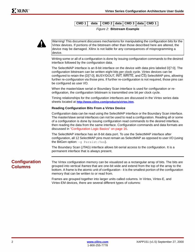
Virtex Series Configuration Architecture User GuideR13
Writing some or all of a configuration is done by issuing configuration commands to the desiredinterface followed by the configuration data
The SelectMAP interface is an 8-bit interface on the device with data pins labeled D[70] Theconfiguration bitstream can be written eight bits per clock cycle Virtex devices can beconfigured to retain the (D[70] BUSYDOUT INIT WRITE and CS) SelectMAP pins allowingfurther re-configuration via those pins If further re-configuration is not required those pins canbe configured as user IO
When the masterslave serial or Boundary Scan interface is used for configuration or re-onfiguration the configuration bitstream is transmitted one bit per clock cycle
Timing relationships for the configuration interfaces are discussed in the Virtex series datasheets located at httpwww xilinxcompr oductsvir texhtm
Reading Configuration Bits From a Virtex Device
Configuration data can be read using the SelectMAP interface or the Boundary Scan interfaceThe masterslave serial interfaces can not be used to read a configuration Reading all or someof a configuration is done by issuing configuration read commands to the desired interfacethen reading the data from the same interface Configuration commands and data formats arediscussed in Configuration Logic Basics on page 16
The SelectMAP interface has an 8-bit data port To use the SelectMAP interface afterconfiguration all 12 SelectMAP pins must remain as SelectMAP as opposed to user IO (usingthe BitGen option -g PersistYes )
The Boundary Scan (JTAG) interface allows bit-serial access to the configuration It is apermanent interface that is always present
ConfigurationColumns
The Virtex configuration memory can be visualized as a rectangular array of bits The bits aregrouped into vertical frames that are one-bit wide and extend from the top of the array to thebottom A frame is the atomic unit of configuration - it is the smallest portion of the configurationmemory that can be written to or read from
Frames are grouped together into larger units called columns In Virtex Virtex-E andVirtex-EM devices there are several different types of columns
CMD 1 data CMD 2 data CMD 3 data CMD 1
Figure 2 Bitstream Example
Warning This document discusses mechanisms for manipulating the configuration bits for theVirtex devices If portions of the bitstream other than those described here are altered thedevice may be damaged Xilinx is not liable for any consequences of misprogramming adevice
2 wwwxilinxcom XAPP151 (v15) September 27 20001-800-255-7778
Virtex Series Configuration Architecture User GuideR13
Each device contains one center column that includes configuration for the four global clockpins Two IOB columns represent configuration for all of the IOBs on the left and right edges ofthe device The majority of columns are CLB columns which each contain one column of CLBsand the two IOBs above and below those CLBs The remaining two column types involve theblock RAM one for content and the other for interconnect For each RAM column one of eachtype is present (for values for all Virtex devices see Table 3 ldquoVirtex Series Devicesrdquo onpage 6)
The columns for an sample Virtex device are shown below
ConfigurationAddressing
Block Type Major Address Minor AddressThe total address space is divided into block types There are two block types RAM and CLBThe RAM type contains only the block SelectRAM content columns (not interconnect) TheCLB type contains all other column types
Both the RAM and CLB address spaces are subdivided into major and minor addresses Eachconfiguration column has a unique major address within the RAM or CLB space Eachconfiguration frame has a unique minor address within its column
The numbering schemes for the block type and minor address are identical between VirtexVirtex-E and Virtex-EM devices The major address numbering scheme differs betweenfamilies and is encapsulated in Table 2 But in both families even major addresses are on theleft half of the device while the odd major addresses are on the right half of the device
Table 1 Configuration Column Type
Column Type of
Frames per Device
Center 8 1
CLB 48 of CLB columns
IOB 54 2
Block SelectRAM Interconnect 27 of Block SelectRAM columns
Block SelectRAM Content 64 of Block SelectRAM columns
2IOB
s
2IOB
s
2GCL
K
2IOB
s
2IOB
s
Left
IOB
Col
umn
(54
fram
es)
Blo
ck S
elec
tRA
MC
onte
nt (
64 fr
ames
)
Blo
ck S
elec
tRA
MIn
terc
onne
ct (
27 fr
ames
)
CLB
Col
umn
(48
fram
es)
hellip
CLB
Col
umn
(48
fram
es)
Cen
ter
Col
umn
(8 fr
ames
)
CLB
Col
umn
(48
fram
es)
hellip
CLB
Col
umn
(48
fram
es)
Blo
ck S
elec
tRA
MIn
terc
onne
ct(2
7 fr
ames
)
Blo
ck S
elec
tRA
MC
onte
nt (
64 fr
ames
)
Rig
ht IO
B C
olum
n(5
4 fr
ames
)
2IOB
s
2IOB
s
2GCL
K
2IOB
s
2IOB
s
Figure 3 Configuration Column Example (XCV50)
XAPP151 (v15) September 27 2000 wwwxilinxcom 31-800-255-7778
Virtex Series Configuration Architecture User GuideR13
Virtex Major Addresses
The CLB address space begins with rsquo0rsquo for the center column and alternates between the rightand left halves of the device for all the CLB columns then IOB columns and finally blockSelectRAM interconnect columns
The RAM address space has lsquo0rsquo for the left block SelectRAM content column and lsquo1rsquo for theright column
A XCV50 is shown in Figure 4 The shaded columns are in the RAM address space
Virtex-EM Major Addresses
The Virtex-EM family has the same numbering as the Virtex family but the block SelectRAMcontent columns begin with 1
Virtex-E Major Addresses
The Virtex-E family has block SelectRAM interspersed between CLB columns Both the CLBand RAM major addressing have been changed to allow for this
The CLB address space again begins with lsquo0rsquo for the center column and alternates between theright and left sides of the device for CLB columns and block SelectRAM interconnect columnsand finally IOB columns The difference is that in Virtex-E devices the block SelectRAM
Table 2 Major Addressing Scheme by Family
Column Type Block Type Virtex Virtex-E Virtex-EM
First MJA CLB 0 0 0
RAM 0 1 1
MJA Order CLB 1 Center2 CLB3 IOB4 BRAM Interconnect
1 Center2 CLB BRAM Interconnect3 IOB
1 Center2 CLB3 IOB4 BRAM Interconnect
RAM BRAM Content BRAM Content BRAM Content
2IOBs
2IOBs
2GCL
K
2IOBs
2IOBs
Left
IOB
Col
umn
(54
fram
es)
Blo
ck S
elec
tRA
MC
onte
nt (
64 fr
ames
)
Blo
ck S
elec
tRA
MIn
terc
onne
ct (
27 fr
ames
)
CLB
Col
umn
(48
fram
es)
hellip
CLB
Col
umn
(48
fram
es)
Cen
ter
Col
umn
(8 fr
ames
)
CLB
Col
umn
(48
fram
es)
hellip
CLB
Col
umn
(48
fram
es)
Blo
ck S
elec
tRA
MIn
terc
onne
ct (
27 fr
ames
)B
lock
Sel
ectR
AM
Con
tent
(64
fram
es
Rig
ht IO
B C
olum
n(5
4 fr
ames
)
2IOBs
2IOBs
2GCL
K
2IOBs
2IOBs
IOLe
ft
RA
M0
BIC
0
C1
C12
Cen
ter
C13
C24
BIC
1
RA
M1
IOR
ight
MA 26 0 28 24 2 0 1 23 27 1 25
Figure 4 Virtex Family Allocation of Frames to Device Resources (XCV50)
4 wwwxilinxcom XAPP151 (v15) September 27 20001-800-255-7778
Virtex Series Configuration Architecture User GuideR13
interconnect appear in the middle of the CLB addresses while in the Virtex and Virtex-EMfamilies they appear at the very end after the IOB columns Also note that the blockSelectRAM content columns begin with lsquo1rsquo (Virtex devices begin with lsquo0rsquo)
A XCV50E is shown in Figure 5 The shaded columns are in the RAM address space
Frames Frames are read and written sequentially with ascending addresses for each operationMultiple consecutive frames can be read or written with a single configuration command Thesmallest amount of data that can be read or written with a single command is a single frameThe entire CLB array plus the IOBs and block SelectRAM interconnect can be read or writtenwith a single command Each block SelectRAM Content must be read or written separately
Frame SizesFrame size depends on the number of rows in the device The number of configuration bits ina frame is 18 times ( CLB_rows+2) and is padded with zeroes on the right (bottom) to fit in 32-bitwords See Frame Organization on page 6 An additional padding word is needed at the endof each frame for pipelining Table 3 shows the frame sizes for all Virtex devices This table alsoshows the size in words of the bitstream for the CLB address space and the number of wordsin each RAM block
2IOB
s
2IOB
s
2IOB
s
2IOB
s
2GCLK
2IOB
s
2IOB
s
Blo
ck S
elec
tRA
MIn
terc
on
ne
ct(2
7 f
ram
es)
2IOB
s
2IOB
s
Blo
ck S
elec
tRA
MC
onte
nt (
64 fr
ames
)
Left
IOB
Col
umn
(54
fram
es)
Blo
ck S
elec
tRA
MC
onte
nt (
64 fr
ames
)B
lock
Sel
ectR
AM
Inte
rco
nn
ect(2
7 f
ram
es)
CLB
Col
umn
(48
fram
es)
hellipC
LB C
olum
n(4
8 fr
ames
)B
lock
Sel
ectR
AM
Con
tent
(64
fram
es)
Blo
ck S
elec
tRA
MIn
terc
on
ne
ct(2
7 f
ram
es)
CLB
Col
umn
(48
fram
es)
hellip
CLB
Col
umn
(48
fram
es)
Cen
ter
Col
umn
(8 fr
ames
)C
LB C
olum
n(4
8 fr
ames
)
hellip
CLB
Col
umn
(48
fram
es)
Blo
ck S
elec
tRA
MC
onte
nt (
64 fr
ames
)C
LB C
olum
n(4
8 fr
ames
)
hellip
CLB
Col
umn
(48
fram
es)
Blo
ck S
elec
tRA
MIn
terc
on
ne
ct(2
7 f
ram
es)
Rig
ht IO
B C
olum
n(5
4 fr
ames
)
2IOB
s
2IOB
s
2IOB
s
2IOB
s
2GCLK
2IOB
s
2IOB
s
2IOB
s
2IOB
s
IOLe
ft
RA
M0
BIC
0
C1
C6
RA
M1
BIC
1
C7
C12
Cen
ter
C13
CLB
18
BIC
2
RA
M2
C19
C24
BIC
3
RA
M3
IOR
ight
MA
30 4 28 26 16 2 14 12 2 0 1 11 13 1 15 25 27 3 29
Figure 5 Virtex-E Family Allocation of Frames to Device Resources (XCV50E)
XAPP151 (v15) September 27 2000 wwwxilinxcom 51-800-255-7778
Virtex Series Configuration Architecture User GuideR13
Frame OrganizationEach frame sits vertically in the device with the ldquofrontrdquo of the frame at the top As shown inFigure 6 it is convenient to consider the frame horizontally when it is viewed as part of abitstream The top IOBs are shown on the left followed by the CLBs in the column and thebottom IOBs on the right Bits in frames are allocated as follows
For CLB columns the first 18 bits control the two IOBs at the top of the column then 18 bits areallocated for each CLB row finally the next 18 bits control the two IOBs at the bottom of the
Table 3 Virtex Series Devices
Device Row times ColBits
FrameWordsFrame
Virtex Virtex-E
RAMCols
of 32-bit Read-backWords (1)
RAMCols
RAMSpace
of 32-bit Read-backWords (1)
CLB(all)
RAM(1 col)
CLB(all)
RAM(1 col)
XCV50 16 times 24 384 12 2 15876 780 - - - -
XCV50E 16 times 24 384 12 - - - 4 6 16524 780
XCV100 20 times 30 448 14 2 22554 910 - - - -
XCV100E 20 times 30 448 14 - - - 4 12 23310 910
XCV150 24 times 36 512 16 2 30384 1040 - - - -
XCV200 28 times 42 576 18 2 39366 1170 - - - -
XCV200E 28 times 42 576 18 - - - 4 12 40338 1170
XCV300 32 times 48 672 21 2 51975 1365 - - - -
XCV300E 32 times 48 672 21 - - - 4 12 53109 1365
XCV400 40 times 60 800 25 2 76275 1625 - - - -
XCV400E 40 times 60 800 25 - - - 4 12 77625 1625
XCV405E 40 times 60 800 25 - - - 14 4 84375 1625
XCV600 48 times 72 960 30 2 108810 1950 - - - -
XCV600E 48 times 72 960 30 - - - 6 12 112050 1950
XCV800 56 times 84 1088 34 2 142902 2210 - - - -
XCV812E 56 times 84 1088 34 - - - 20 4 159426 2210
XCV1000 64 times 96 1248 39 2 186381 2535 - - - -
XCV1000E 64 times 96 1248 39 - - - 6 12 190593 2535
XCV1600E 72 times 108 1376 43 - - - 8 12 237231 2795
XCV2000E 80 times 120 1536 48 - - - 8 12 292464 3120
XCV2600E 92 times 138 1728 54 - - - 8 12 375678 3510
XCV3200E 104 times 156 1952 61 - - - 8 12 477081 3965
Notes1 Includes pad frame in calculation
6 wwwxilinxcom XAPP151 (v15) September 27 20001-800-255-7778
Virtex Series Configuration Architecture User GuideR13
CLB column The frame then contains enough ldquopadrdquo bits to make it an integral multiple of 32bits
For IOB columns the frame allocates 18 bits per three IOB rows Figure 7 When reading andwriting frames bits are grouped into 32-bit words starting on the left (corresponding to the topof the device) If the last word does not completely fill a 32-bit word it is padded on the right withzeroes
For block SelectRAM content columns (Figure 8) the first 18 bits are pad bits then 72 bits areallocated for each RAM row finally there are another 18 pad bits The frame then adds enoughldquopadrdquo bits to make it an integral multiple of 32 bits
Location of LUT SelectRAM BitsWith respect to the beginning of a configuration frame relative locations of LUT SelectRAM bitswithin the bitstream are the same for every CLB slice The bits of a LUT SelectRAM are spreadacross 16 consecutive frame Minor Addresses Each frame Minor Address contains allinstances of a single bit index for that column These 16 frames contain all 16 bits of the LUTSelectRAM for a column of CLB slices You must read or write the 16 frames containing thosebits to read or write the entire LUT SelectRAM
Figure 6 CLB Column Frame Organization
Figure 7 IOB Column Frame Organization
Figure 8 Block SelectRAM Content Column Frame Organization
Note LUT SelectRAM bits are stored inverted Flip-Flop data are stored in their true senseWhen reading or writing LUT SelectRAM data from the bitstream it is negated from the logicsense of the data For example a 4-input AND gate has the truth tableLUT[150] = 1000000000000000
This truth table isstored internally in theLUTSelectRAMasLUT[150] = 0111111111111111Ofcourse user logic reading the data from the LUT SelectRAM would read the correct logicvalue LUT[150] = 1000000000000000
Top 2 IOBs13 Bottom 2 IOBs1313
CLB Rn1313
13 18131813181318131813
CLB R213CLB R113
x151_06_020700
Top 3 IOBs Bottom 3 IOBs1313
181818
3 IOBs
x151_07_020800
Pad PadRAM Rn
1872727218
RAM R1RAM R0
x151_08_021800
XAPP151 (v15) September 27 2000 wwwxilinxcom 71-800-255-7778
Virtex Series Configuration Architecture User GuideR13
ConfigurationData Operations
Reading Configuration DataConfiguration information can be read from the Virtex devices if readback is enabled in thecurrent configuration (See the description of the Control Register field SBITS on page 21)CLB and IOB configuration data can be read while the device is operating
When reading data from a Virtex device a pad frame is read before any of the data framesThis is in addition to the pad word in each data frame The pad frame must be included in theword count to be read from the device
Each frame read from the device consists of the number of words shown in Table 3
For example the XCV150 has 16-word frames When reading frames the first word of a frameis a pad word Including the pad frame the XCV150 has 1899 (3038416) frames (SeeFigure 9)
Writing Configuration DataConfiguration information can be written to a Virtex device while the device is running if writingis enabled in the current configuration (See the Control Register field SBITS in Table 23) Re-writing the same configuration data does not generate any transient signals
Changing configuration data may generate transient signals especially if LUT values or signalrouting is changed For this case all the logic cells and routing can be placed in a non-contentious state by asserting the GHIGH_B signal See the description for the CommandRegister (CMD) on page 18
When writing configuration data to the Virtex device whether from the SelectMAP or JTAGinterfaces the data frames are written to the device with each frame followed by a pad wordAfter all the data frames are written a pad frame must be written (to flush internal pipelines)The pad words and pad frame must be included in the number of words to be written to thedevice (Table 3)
For example the XCV1000 has 39-word frames When writing frames the last word of theframe is a pad word Including the pad frame the XCV1000 has 4779 (18638139) framesSee Figure 10)
Altering Configuration DataVirtex devices support the Read-Modify-Write (RMW) method of changing LUT SelectRAMdata Therefore it is possible to read or alter the contents of one or more LUT SelectRAMsthrough the JTAG or SelectMAP interfaces When writing data to one or more LUTSelectRAMs all the bits in the frame must have valid configuration information This can beassured by altering valid configurations from bitstream files or from frames read from a properlyconfigured Virtex device When using the RMW method it may be expeditious to read the dataignoring the pad frame and the pad word of only the first frame This aligns the remaining
Pad Frame (16 words)Pad Word Data Frame 0 (15 words)
hellip
hellip
Pad Word Data Frame n (15 words)
Figure 9 XCV150 Frame Padding for Device Read
Data Frame 0 (38 words) Pad Word
hellip
Data Frame n (38 words) Pad WordPad Frame (39 words)
Figure 10 XCV1000 Frame Padding for Device Write
8 wwwxilinxcom XAPP151 (v15) September 27 20001-800-255-7778
Virtex Series Configuration Architecture User GuideR13
configuration data in the Device Write format After modifying the configuration the altered datacan be written to the Virtex device followed by a pad word and a pad frame
It is not necessary to retain the contents of the pad frame or pad words However pad wordsand pad frames are included in the CRC calculation
Definitions Two sets of variables are defined to determine where a desired bit is in the configuration dataThe first is a set of ldquoindependentrdquo variables or design attributes namely characteristics of thedesign that are known ie the device size and which CLB and bit(s) within the CLB to locateTable 4 The second set is a set of ldquodependentrdquo variables or design variables namely valuesthat must be calculated to find the bit(s) of interest listed in Table 5
Note Frames span an entire column of CLB slices (or IOBs) Thus when changing LUTSelectRAM bit 0 for a single CLB slice (eg R3C4S1) LUT SelectRAM bit 0 for all slices inthat column (ie RC4S1) is written with the same command One must ensure that either allother data in the slice is constant or changed externally through partial configurations
LUT SelectRAMs not configured externally should not lie in the same slice with LUTs or LUTSelectRAMs that are re-configured externally Such a mixture can cause the unrelated LUTSelectRAM data to be re-configured when the frames are written to the device Figure 11shows what can happen if this restriction is not observed
In this example it is the objective to perform a Read-Modify-Write on the LUT SelectRAM inR2C3S1 in column 3 which is shown in the first column in the figure Row 2 contains a LUTcontaining the value AB Row 3 contains a SelectRAM containing the value C3 Because theRead and Write operations operate on an entire frame the RAM in R3C3S1 is also read andwritten when R2C3S1 is read and written Performing the Readback operation reads all theLUT and SelectRAM values for the column Before the new value for the LUT is written it ispossible for the on-chip circuitry to write a new value such as 14 into the SelectRAM Whenthe new value BD is written via the configuration interface into LUT R2C3S1 the value C3 isalso written into RAM R3C3S1 This may not always be desirable (It is design-dependent)
Figure 11 Potential Write Conflicts
x151_11_020800
LUT R2C3S113AB13
RAM R3C3S113C313
Before13Readback
13
LUT R2C3S113AB13
RAM R3C3S1131413
Before13Configuration 13
Write
13
LUT R2C3S113BD13
RAM R3C3S113C313
After13Configuration13
Write
13
Table 4 Design Attributes (Independent Variables)
Term Definition
Chip_Cols of CLB columns on the Virtex device
Chip_Rows of CLB rows on the Virtex device
Chip_Rams of block SelectRAM columns on the Virtex device
RAM_Space Spacing of block SelectRAM columns (in terms of CLB columns)
FL of 32-bit words in the frame
XAPP151 (v15) September 27 2000 wwwxilinxcom 91-800-255-7778
Virtex Series Configuration Architecture User GuideR13
RW 1 for Read 0 for Write
CLB_Col Column number of the desired CLB
CLB_Row Row number of the desired CLB
Slice 0 or 1
FG 0 for the F-LUT 1 for the G-LUT
lut_bit The desired bit from the given LUT Bits in the LUT are indexed from 0 to 15
XY 0 for the X Flip-Flop 1 for the Y Flip-Flop
RAM_Col Column number of the desired block SelectRAM
RAM_Row Row number of the desired block SelectRAM
ram_bit The desired bit from the given block SelectRAM Bits are indexed from 0 to4095
Table 5 Design Variables (Dependent Variables)
Term Definition
MJA Frame Major Address
MNA Frame Minor Address
fm_st_wd The index of the word within a full configuration segment that correspondsto the starting word of the desired frame A full configuration segment isdefined as the following 1) for CLBIOB all CLB IOB and RAMinterconnect frames beginning at MJA=0 MNA=0 and 2) for blockSelectRAM all RAM content frames for the given RAM column Words arenumbered starting at 0
fm_wd The index of the 32-bit word within a frame that contains the desired bitWords in a frame are numbered starting at 0
fm_wd_bit_idx The bit index of the desired bit within frame word fm_wd Words areindexed in ldquobig-endianrdquo style with bit 31 on the left and bit 0 on the right
fm_bit_idx Bit index within a frame of the desired bit Numbered starting with 0 as theleft-most (first) bit Bit numbering within a frame continues across all thewords in the frame
Table 6 Functions used in Equations
Functions Definition
floor(x) The largest integer not larger than x Eg floor(31) = 3 because the nextlargest integer 4 is larger than 31 floor(3)=3
ceiling(x) The smallest integer greater than or equal to x For example ceiling(32) = 4because 4 is greater than 32 and 3 is not ceiling (4) = 4
The modulus operation 5 2 = 1 5 3 = 2 5 5 = 0
Table 4 Design Attributes (Independent Variables) (Continued)
Term Definition
10 wwwxilinxcom XAPP151 (v15) September 27 20001-800-255-7778
Virtex Series Configuration Architecture User GuideR13
CLB LUTSelectRAMDependentVariables
Table 7 shows equations for the LUT SelectRAM ldquoDependent Variablesrdquo that were defined inTable 5
Virtex-E CLB LUT SelectRAM Dependent VariablesThe additional block SelectRAM columns in Virtex-E devices require an adjustment to the MJAThe following equations calculate the adjustment necessary for each of the affected dependentvariables For each variable calculate the base value based upon the Virtex equations onlyand then add the resulting Virtex adjustment
The left and right sides of the device are treated differently
LUT SelectRAM ExamplesSee ldquoExamplesrdquo on page 27 for several examples of reading and evaluating configuration dataThe examples illustrate how to make use of these equations to find the desired data in abitstream
Table 7 Virtex Equations for LUT SelectRAM Dependent Variables
Term Definition
MJA if (CLB_Col le Chip_Cols2)then Chip_Cols ndash CLB_Col times 2 + 2else 2 times CLB_Col ndash Chip_Cols ndash 1
MNA lut_bit + 32 ndash Slice times (2 times lut_bit + 17)
fm_bit_idx 3 + 18 times CLB_Row ndash FG + RW times 32
fm_st_wd FL times (8 + (MJA ndash1) times 48 + MNA) + RW times FL
fm_wd floor(fm_bit_idx32)
fm_wd_bit_idx 31 + 32 times fm_wd ndash fm_bit_idx
Notes
bull Do NOT input the final results back into the original Virtex equations (eg do not useMJAfinal value to calculate fm_st_wd)
bull MJAfinal = MJA + MJA_adj
bull fm_st_wdfinal = fm_st_wd + fm_st_wd_adj
Table 8 CLB Location
CLB Location CLB Column
Left CLB_Col le Chip_Cols2
Right CLB_Col gt Chip_Cols2
Table 9 Virtex-E Families Adjustments for LUT SelectRAM Dependent Variables
Term Definition
MJA_adj Left RAM_Bound = (Chip_Rams2 - 1) x RAM_SpaceMJA_adj = 2 x ceiling((RAM_Bound - CLB_Col + 1) RAM_Space)
Right
RAM_Bound = Chip_Cols - (Chip_Rams2 - 1) x RAM_Space + 1MJA_adj = 2 x ceiling((CLB_Col - RAM_Bound + 1) RAM_Space)
fm_st_wd_adj FL times (27 x MJA_adj)
XAPP151 (v15) September 27 2000 wwwxilinxcom 111-800-255-7778
Virtex Series Configuration Architecture User GuideR13
CLB Flip-FlopDependentVariables
Equations for the CLB flip-flops can be found in Table 10 Their locations are calculatedsimilarly to the LUT SelectRAM locations Equations for the CLB FF Dependent Variables aredefined in Table 5
Virtex-E CLB Flip-Flop Dependent VariablesApply the adjustments given in Table 8 and Table 9
IOB DependentVariables
Each IOB contains four values that can be captured into special registers These values are
bull I mdash the input flip-flop
bull O mdash the output flip-flop
bull T mdash the flip-flop for the tri-state control
bull P mdash the value of the IO pad
These values are captured by utilizing the CAPTURE_VIRTEX symbol in your design TheLibraries Guide has more details on the use of this symbol The following registers will be readas part of the readback data
Access to the IOB flip-flops is different for the top and bottom IOBs versus the left and rightIOBs
The top and bottom IOBs are part of the CLB column frames There are two IOBs at the top andbottom of each CLB column
The left and right IOBs are in columns by themselves There are three IOBs per CLB row
IOBs are numbered clockwise around the die Pad 1 is located at the left side of the top edgeabove CLB column 1 The equations for where to find IOB flip-flops in the bitstream are basedon the pad number which is the same for a given size device not the package pin name whichvaries from package to package The mapping from package pin names to pad numbers canbe found in EPIC or fpga_editor
Table 11 contains the numeric pad indices for the pads on all four edges of the device in termsof the number of CLB columns and rows on the device
Table 10 Virtex Equations for CLB FF Dependent Variables
Term Definition
MJA if (CLB_Col le Chip_Cols2)then Chip_Cols ndash CLB_Col times 2 + 2else 2 times CLB_Col ndash Chip_Cols ndash 1
MNA Slice times (12 times XY ndash 43) ndash 6 times XY + 45
fm_bit_idx (18 times CLB_Row) + 1 + (32 times RW)
fm_st_wd FL times (8 + (MJA ndash1) times 48 + MNA) + RW times FL
fm_wd floor(fm_bit_idx32)
fm_wd_bit_idx 31 + 32 times fm_wd ndash fm_bit_idx
12 wwwxilinxcom XAPP151 (v15) September 27 20001-800-255-7778
Virtex Series Configuration Architecture User GuideR13
Table 12 shows the equations for the dependent variables for the IOB flip-flops The variable iin this table refers to the index of pad i
Table 11 IOB Pad Indices
PadLocation Pad Index i
Top 1 le i le Chip_Cols times 2
Right Chip_Cols times 2 +1 le i le Chip_Cols times 2 + Chip_Rows times 3
Bottom Chip_Cols times 2 + Chip_Rows times 3 + 1 le i le Chip_Cols times 4 + Chip_Rows times 3
Left Chip_Cols times 4 + Chip_Rows times 3 + 1 le i le Chip_Cols times 4 + Chip_Rows times 6
Table 12 Equations for IOB Dependent Variables
Term Definition
MJA
Topif (i le Chip_Cols)then Chip_Cols ndash ceiling(i2) times 2 + 2else 2 times ceiling (i2) ndash Chip_Cols ndash1
Right Chip_Cols + 1
Bottomif (i gt 3 times (Chip_Cols + Chip_Rows))then 2 times ceiling((i ndash 3 times Chip_Cols ndash 3 times Chip_Rows)2)else Chip_Cols ndash 2 times floor((i ndash 2 times Chip_Cols ndash 3 times Chip_Rows ndash 1)2) ndash 1
Left Chip_Cols + 2
MNA
Top
I ndash 25 times (i2) + 45
O ndash 13 times (i2) + 39
T ndash 5 times (i2) + 35
P ndash 4 times (i2) + 25
Right
I t = (i ndash 2 times Chip_Cols) 3 MNA = 275 times t2 ndash 575 times t + 32
O t = (i ndash 2 times Chip_Cols) 3 MNA = 215 times t2 ndash 515 times t + 38
T t = (i ndash 2 times Chip_Cols) 3 MNA = 175 times t2 ndash 475 times t + 42
P 50
Bottom
I 25 times ((i ndash 2 x Chip_Cols - 3 x Chip_Rows)2) + 20
O 13 times ((i ndash 2 x Chip_Cols - 3 x Chip_Rows)2) + 26
T 5 times ((i ndash 2 x Chip_Cols - 3 x Chip_Rows)2) + 30
P 4 times ((i ndash 2 x Chip_Cols - 3 x Chip_Rows)2) + 21
Left
I t = (i ndash 4 x Chip_Cols - 3 x Chip_Rows)3 MNA = 175 times t2 ndash 475 times t + 45
O t = (i ndash 4 x Chip_Cols - 3 x Chip_Rows)3 MNA = 235 times t2 ndash 535 times t + 39
T t = (i ndash 4 x Chip_Cols - 3 x Chip_Rows)3 MNA = 275 times t2 ndash 575 times t + 35
P 50
XAPP151 (v15) September 27 2000 wwwxilinxcom 131-800-255-7778
Virtex Series Configuration Architecture User GuideR13
Virtex-E IOB Dependent VariablesSimilar to CLB dependent variables only the variables affected by the major address aredifferent in Virtex-E and Virtex-EM devices versus Virtex devices A simple way to account forthe change is to determine the CLB column where the pad resides (only true for top andbottom) Then the adjustment calculated for the CLB column can be applied The conversionto CLB columns is found in Table 13
fm_bit_idx
Top 32 times RW
Right
I O ampT 18 times (1 + floor ((i ndash 2 times Chip_Cols ndash 1)3)) + 32 times RW
Pt = (i ndash 2 times Chip_Cols) 3fm_bit_idx = 18 times (1 + floor ((i ndash 2 times Chip_Cols ndash 1)3)) + 6 times t2 ndash 17 times t + 15 + 32 timesRW
Bottom 18 times (Chip_Rows + 1)+ 32 times RW
Left
I O ampT18 times (Chip_Rows ndash floor((i ndash 4 times Chip_Cols ndash 3 times Chip_Rows ndash 1)3)) + 32 times RW
Pt = (i ndash 4 times Chip_Cols ndash 3 times Chip_Rows)3fm_bit_idx = 18 times (Chip_Rows ndash floor ((i ndash 4 times Chip_Cols ndash 3 times Chip_Rows ndash 1)3))ndash 105 times t2 + 215 times t + 4 + 32 times RW
fm_st_wdif (MJA gt Chip_Cols + 1)then FL times (54 times MJA ndash 46 + MNA ndash 6 times Chip_Cols) + RW times FLelse FL times (8 + (MJA ndash1) times 48 + MNA) + RW times FL
fm_wd floor (fm_bit_idx32)
fm_wd_bit_idx 31 + 32 times fm_wd ndash fm_bit_idx
Table 12 Equations for IOB Dependent Variables (Continued)
Term Definition
Table 13 Pad -gt CLB Column
Term Definition
CLB_ColTop ceiling(i2)
Bottom ceiling((4 x Chip_Cols + 3 x Chip_Rows + 1 - i)2)
Table 14 Virtex-E Families Adjustments for IOB Dependent Variables
Term Definition
MJA_adj
Top use Table 8 and Table 9
Right Chip_Rams
Bottom use Table 8 and Table 9
Left Chip_Rams
fm_st_wd_adj FL times (27 x MJA_adj)
14 wwwxilinxcom XAPP151 (v15) September 27 20001-800-255-7778
Virtex Series Configuration Architecture User GuideR13
BlockSelectRAMDependentVariables
The equations for the block SelectRAM dependent variables are given in Table 15 Therelationship of a particular memory cell index in the context of a given configuration is describedin XAPP130 ldquoUsing the Vir tex Bloc k SelectRAM+ Resour cerdquo
Virtex-E Block SelectRAM Dependent VariablesThe RAM major address numbering scheme changed slightly such that the lowest MJA on theleft side is now 2 instead of 0 As in the case for the CLB equations the adjustments belowshould be applied after the Virtex equations
Table 15 Virtex Equations for Block SelectRAM Dependent Variables
Term Definition
MJAif (RAM_Col lt Chip_Rams2)then 2 x (Chip_Rams2 - 1 - RAM_Col)else 2 x (RAM_Col - Chip_Rams2) + 1
MNA
1 x floor(((ram_bit 64) 64)32) + 2 x floor(((ram_bit 64) 32)16)+ 4 x floor(((ram_bit 64) 16)8) + 8 x floor(((ram_bit 64) 8)4)+ 16 x floor(((ram_bit 64) 4)2) + 32 x floor(((ram_bit 64) 2)1)equivalent to MNA = div64[05] where div64[50] = floor(ram_bit64)
fm_bit_idxobtain value for bitpos from Table 16
fm_bit_idx = 18 + 72 x RAM_Row + bitpos
fm_st_wd FL times MNA + RW times FL
fm_wd floor(fm_bit_idx32)
fm_wd_bit_idx 31 + 32 times fm_wd ndash fm_bit_idx
Table 16 Virtex Block SelectRAM Bit Position Within a Given Block SelectRAM
ram
_bit
6
4
bitp
os
ram
_bit
6
4
bitp
os
ram
_bit
6
4
bitp
os
ram
_bit
6
4
bitp
os
ram
_bit
6
4
bitp
os
ram
_bit
6
4
bitp
os
ram
_bit
6
4
bitp
os
ram
_bit
6
4
bitp
os
0 42 8 45 16 29 24 26 32 43 40 44 48 28 56 27
1 58 9 61 17 13 25 10 33 59 41 60 49 12 57 11
2 41 10 46 18 30 26 25 34 40 42 47 50 31 58 24
3 57 11 62 19 14 27 9 35 56 43 63 51 15 59 8
4 50 12 53 20 21 28 18 36 51 44 52 52 20 60 19
5 49 13 54 21 22 29 17 37 48 45 55 53 23 61 16
6 66 14 69 22 5 30 2 38 67 46 68 54 4 62 3
7 65 15 70 23 6 31 1 39 64 47 71 55 7 63 0
Table 17 Virtex-E and Virtex-EM Adjustments for Block SelectRAM DependentVariables
Term Definition
MJA_adj if (RAM_Col lt Chip_Rams2) MJA_adj = 2
XAPP151 (v15) September 27 2000 wwwxilinxcom 151-800-255-7778
Virtex Series Configuration Architecture User GuideR13
ConfigurationLogic Basics
Configuration DataConfiguration data is organized as 32-bit words There are two major commands that theconfiguration data can contain Read and Write A configuration command is executed whenthe configuration command is read or written to the appropriate command register
The OP field contains 01 for a Read operation and 10 for a Write operation (See Figure 12)
A command is organized as a packet with a header word and optional data words The headerword is the first word written to the appropriate command register for a read or write operationThe header word contains a type field (001) an operand field a register address field and aword count field The format for the command header is shown in Figure 13 on page 17
The Register Address field defines the target of this command as defined in Table 18 on page17
The header word count field contains an integer between 0 and 2047 and indicates thenumber of words that follow the header Larger word counts (between 2048 and 1048575words) are achieved by setting the header word count to 0 The Extension header word has atype field = 010 an OP field that must match the OP field in the preceding Command Headerword and a 20-bit word count this format is shown Figure 14 on page 17
Configuration FlowVirtex devices are configured by presenting configuration data to the SelectMAP or JTAGinterfaces in a specific sequence
For Initial Configuration
1 Issue one or more pad words (SelectMAP only)
2 Issue Sync word (SelectMAP only)
3 Reset CRC
4 Set FLR
5 Set COR
6 Set MASK
7 Set CTL (Set PERSIST if you want to keep SelectMAP active after this configuration)
8 Issue a SWITCH (switch CCLK frequency) command to the CMD register This isnecessary only in Master Serial configuration mode
Reading Configuration
These commands can be issued to read a full configuration or for a partial configuration afterthe device has been completely configured
1 Issue a Sync word (SelectMAP only) if the previous configuration command was aborted
2 Set the FAR to the starting address
3 Issue a RCFG (read configuration) command to the CMD register
4 Write the number of words to be read to the FDRO register
5 Flush the command pipeline with a pad word
6 Read data frames
OP CODERead 01Write 10
Figure 12 OP Field Code
16 wwwxilinxcom XAPP151 (v15) September 27 20001-800-255-7778
Virtex Series Configuration Architecture User GuideR13
Writing Configuration
These commands can be issued either as part of an initial configuration or for a partialconfiguration after the device has been configured
1 Issue a Sync word (SelectMAP only) if the previous configuration command was aborted
2 If the frames being written can cause contention then assert the GHIGH_B signal
3 Set the FAR to the starting address
4 Issue a WCFG (write configuration) command to the CMD register
5 Write the number of words to be written to the FDRI register
6 Write data frames
7 If the GHIGH_B signal was asserted de-assert it by writing the LFRM (Last Frame)command to the CMD register and write one pad frame
ConfigurationRegisters
Configuration logic is accessed and controlled via a collection of 32-bit registers called theconfiguration registers (see Table 18) Registers are described in the following sections
Type OP Register Address RSV Word Count31 30 29 28 27 26 25 24 23 22 21 20 19 18 17 16 15 14 13 12 11 10 9 8 7 6 5 4 3 2 1 00 0 1 x x 0 0 0 0 0 0 0 0 0 0 x x x x 0 0 x x x x x x x x x x x
Notes1 Locations within fields containing a zero or one must have these values An X in a bit field indicates that the value is variable and must
be set2 Heavy vertical lines are used to separate fields Light vertical lines separate nibbles in the word
Figure 13 Command Header Format
Type OP Word Count31 30 29 28 27 26 25 24 23 22 21 20 19 18 17 16 15 14 13 12 11 10 9 8 7 6 5 4 3 2 1 00 1 0 x x 0 0 0 0 0 0 0 x x x x x x x x x x x x x x x x x x x x
Notes1 Locations within fields containing a zero or one must have these values An X in a bit field indicates that the value is variable and must
be set2 Heavy vertical lines are used to separate fields Light vertical lines separate nibbles in the word
Figure 14 Large Block Count Header Extension Format
Table 18 Configuration Register Addresses
Register Name Mnemonic RW Binary Address
CRC CRC RW 0000
Frame Address FAR RW 0001
Frame Data Input FDRI W 0010
Frame Data Output FDRO R 0011
Command CMD RW 0100
Control CTL RW 0101
Control Mask MASK RW 0110
Status STAT R 0111
Legacy Output LOUT W 1000
XAPP151 (v15) September 27 2000 wwwxilinxcom 171-800-255-7778
Virtex Series Configuration Architecture User GuideR13
Command Register (CMD)The content of the Command Register (CMD) is interpreted by the configuration state machineConfiguration commands control the operation of the configuration state machine the FrameData Register (FDR) and some of the global signals The command in the Command Registeris executed each time the FAR is loaded with a new value The effect of each command isdefined in Table 19
Configuration Option COR RW 1001
Reserved mdash mdash 1010
Frame Length FLR RW 1011
Reserved mdash mdash 1100
Reserved mdash mdash 1101
Reserved mdash mdash 1110
Reserved mdash mdash 1111
Table 18 Configuration Register Addresses (Continued)
Register Name Mnemonic RW Binary Address
Table 19 Configuration Commands
Cmd Code Description
Rsvd 0000 Reserved
WCFG 0001Write Configuration Data mdash Used prior to writing configuration data to the FDRI It takes theinternal configuration state machine through a sequence of states that control the shifting of the FDRand the writing of the configuration memory (See Frame Data Input Register (FDRI) on page 24)
Rsvd 0010 Reserved
LFRM 0011Last Frame mdash This command is loaded prior to writing the last (pad) data frame if the GHIGH_Bsignal was asserted This command is not necessary if the GHIGH_B signal was not asserted Thisallows overlap of the last frame write with the release of the GHIGH_B signal
RCFG 0100Read Configuration Data mdash Used prior to reading frame data from the FDRO Similar to the WCFGcommand in its effect on the FDR (see Frame Data Output Register (FDRO) on page 24)
START 0101Begin Startup Sequence mdash Starts the startup sequence This command is also used to start ashutdown sequence prior to partial re-configuration The Startup Sequence begins with the nextsuccessful CRC check (see Cyclic Redundancy Check (CRC) on page 22)
RCAP 0110Reset Capture mdash Used when performing capture in single-shot mode This command must be usedto reset the capture signal if single-shot capture has been selected
RCRC 0111 Reset CRC mdash Used to reset CRC register (see Cyclic Redundancy Check (CRC) on page 22)
AGHIGH 1000Assert GHIGH_B Signal mdash Used prior to re-configuration to prevent contention while writing newconfiguration data All CLB outputs and signals are forced to a one
SWITCH 1001Switch CCLK Frequency mdash Used to change (increase) the frequency of the Master CCLK Thenew frequency is specified in Table 21
Rsvd 1010 Reserved
Rsvd 1011 Reserved
Rsvd 1100 Reserved
18 wwwxilinxcom XAPP151 (v15) September 27 20001-800-255-7778
Virtex Series Configuration Architecture User GuideR13
Configuration Option Register (COR)The Configuration Option Register (COR) is used to select configuration options that areillustrated in Figure 15 and defined in Table 20 Entries in this table are further explained in thefollowing tables
Rsvd 1101 Reserved
Rsvd 1110 Reserved
Rsvd 1111 Reserved
Table 19 Configuration Commands (Continued)
Cmd Code Description
DO
NE
_PIP
E
DR
IVE
_DO
NE
SIN
GLE
OS
CF
SE
L
SS
CLK
SR
C
LOC
K_W
AIT
SH
UT
DO
WN
DO
NE
_CY
CLE
LCK
_CY
CLE
GT
S_C
YC
LE
GW
E_C
YC
LE
GS
R_C
YC
LE
31 30 29 28 27 26 25 24 23 22 21 20 19 18 17 16 15 14 13 12 11 10 9 8 7 6 5 4 3 2 1 00 x x x x x x x x x x x x x x x x x x x x x x x x x x x x x x x
Notes1 Locations within fields containing a zero or one must have these values An X in a bit field indicates that the value is variable and must
be set2 Heavy vertical lines are used to separate fields Light vertical lines separate nibbles in the word
Figure 15 COR (Configuration of Option Register) Fields
XAPP151 (v15) September 27 2000 wwwxilinxcom 191-800-255-7778
Virtex Series Configuration Architecture User GuideR13
Table 21 shows the allowed values for the OSCFSEL field of the COR Setting OSCFSEL toone of these values will set the Master CCLK frequency to the specified value
Table 20 Configuration Option Register Fields
Field Bit Indices DescriptionBitgenDefault
DONE_PIPE 30
0 No pipeline stage for DONEIN
1 Add pipeline stage to DONEINFPGA waits on DONE that is delayed by one (1) cycle of the StartupClkrather than the pin itself Use this option when StartupClk is running at highspeeds
0
DRIVE_DONE 290 DONE pin is open drain
1 DONE pin is actively driven high0
SINGLE 28 Readback capture is one-shot 0
OSCFSEL 2722 Select CCLK frequency in Master Serial configuration mode 2
SSCLKSRC 2120
Startup sequence clock source00 Cclk01 UserClk1x JTAGClk
0
LOCK_WAIT 1916
4-bit mask indicating which DLL lock signals to wait for during LCK cycleThe 4 bits (from MSB to LSB) correspond to DLLs TL=3 TR=2 BL=1BR=0 (top-left top-right etc) In Virtex-E devices where there are 8 DLLseach mask bit applies to the 2 DLLs in that quadrant of the device Thedefault is not to wait for any DLL lock signals
0
SHUTDOWN 15
Indicate whether doing a startup or shutdown sequence
0 Startup
1 Shutdown sequence
0
DONE_CYCLE 1412 Startup phase in which DONE pin is released 3
LCK_CYCLE 119 Stall in this startup phase until DLL locks are asserted 7
GTS_CYCLE 86 Startup phase in which IOs switch from tri-state to user design 4
GWE_CYCLE 53 Startup phase in which the global write-enable is asserted 5
GSR_CYCLE 20 Startup phase in which the global setreset is negated 5
Table 21 OSCFSEL-Specified Master CCLK Frequencies)
CCLK(MHz) OSCFSEL
CCLK(MHz) OSCFSEL
CCLK(MHz) OSCFSEL
43 000010 13 001010 41 100111
54 010001 15 001101 45 110011
69 000100 20 010111 51 101010
81 000101 26 011010 55 110100
20 wwwxilinxcom XAPP151 (v15) September 27 20001-800-255-7778
Virtex Series Configuration Architecture User GuideR13
Table 22 shows the values of the DONE_CYCLE LCK_CYCLE GTS_CYCLE GWE_CYCLEand GSR_CYCLE fields in COR This table shows the step in the start-up sequence when eachof these signals becomes active
Control Register (CTL)The Control Register (CTL) fields are illustrated in Figure 16 on page 21 and defined inTable 23
92 000110 30 011101 60 101101
100 000111 34 110010 mdash mdash
Notes1 These values are accurate to +45 ndash 30
Table 22 COR Startup Cycle Fields
FieldValue
DONE_CYCLE(DONE Active)
GTS_CYCLE(GTS_CFGInactive)
GSR_CYCLE(GSR Inactive)
GWE_CYCLE(GWE Active) LCK_CYCLE
000 1 1 1 1 0
001 2 2 2 2 1
010 3 3 3 3 2
011 4 (default) 4 4 4 3
100 5 5 (default) 5 5 4
101 6 6 6 (default) 6 (default) 5
110 mdash DoneIndagger DoneIndagger DoneIndagger 6
111 Keep State Keep State Keep State Keep State Donrsquot Wait(default)
Notes1 dagger DONE if DonePipe = No else the delayed version of DONE
Table 21 OSCFSEL-Specified Master CCLK Frequencies) (Continued)
CCLK(MHz) OSCFSEL
CCLK(MHz) OSCFSEL
CCLK(MHz) OSCFSEL
SB
ITS
PE
RS
IST
GT
S_U
SR
_B
31 30 29 28 27 26 25 24 23 22 21 20 19 18 17 16 15 14 13 12 11 10 9 8 7 6 5 4 3 2 1 00 0 0 0 0 0 0 0 0 0 0 0 0 0 0 0 0 0 0 0 0 0 0 x x x 0 0 0 0 0 x
Notes1 Locations within fields containing a zero or one must have these values An X in a bit field indicates that the value is variable and must
be set2 Heavy vertical lines are used to separate fields Light vertical lines separate nibbles in the word
Figure 16 Control Register Fields
XAPP151 (v15) September 27 2000 wwwxilinxcom 211-800-255-7778
Virtex Series Configuration Architecture User GuideR13
Cyclic Redundancy Check (CRC)A data input error checking mechanism is provided through the Cyclic Redundancy Check(CRC) register When data is written to any configuration register (except LOUT) a 16-bit CRCvalue is calculated using both the register data and the address This value is saved in the CRCregister At the end of any series of writes a pre-calculated CRC block-check value may bewritten to the CRC register If the resulting value is non-zero an error is indicated TheCRC_ERROR bit is accessible through the status register If a CRC error is detectedconfiguration logic is put in the ERROR mode The following section is an algorithm forcomputing CRC
CRC Algorithm Initialization bcc = 0skip_pad = truemore_words = true Check for write operation do
w = next_wordif (w[3127] == rsquo00101rsquo)
A Read OP Donrsquot use in CRCwc = w[100]if (wc == 0)
w = next_wordwc = w[190]
while (wc-- gt 0)
w = next_word
elsif (w[3127] == rsquo00110rsquo)
A Write OP Use in CRC addr = w[1613]if (addr Π0124569DB)
wc = w[100]if (wc == 0)
wc is in next word w = next_wordwc = w[190]
while (wc-- gt 0)
w = next_wordsw[350] = addr wordfor (i=0 ilt36 i++)
Table 23 Control Register Bits
NameBit
Indices Description
SBITS 87 Security level0 ReadWrite OK (default)1 Readback disabled23 Readback disabled Writing disabled except CRCregister
PERSIST 6 Configuration interface remains after configuration0 No (default)1 Yes
GTS_USR_B 0 Active-low global tristate IOs Turn off pull-ups ifGTS_CFG_B is also asserted
22 wwwxilinxcom XAPP151 (v15) September 27 20001-800-255-7778
Virtex Series Configuration Architecture User GuideR13
x16 = bcc[15] XOR sw[i]x15 = bcc[14] XOR x16x2 = bcc[1] XOR x16bcc[150] =
x15bcc[132]x2bcc[0]x16 Note the bit order crc[150] = bcc[015]
else
Pad word - ignore
while (more_words)
Frame Address Register (FAR)The Frame Address Register (FAR) holds the address of the current frame The address isdivided into three parts the block type the major address and the minor address The blocktype field indicates whether the CLB or block RAM address space is used The command in thecommand register is executed each time the FAR is loaded with a new value
The major address selects the CLB or RAM column the minor address selects the frame withinthe column The minor address is incremented each time a full data frame is read from orwritten to the frame data register If the last frame within the CLB column is selected when theincrement occurs the major address is incremented and the minor address is reset to zerootherwise the minor address is incremented However the block RAM major address is notincremented automatically
See Figure 18 for the definitions of valid values for the block type field The FAR field definitionsare shown in Figure 19
Figure 17 CRC Calculation Register
Note the Block RAM Major Address is not incremented automatically To address a differentBlock RAM Content column the FAR must be loaded with the new Major Address
Type CodesCLB 00RAM 01
Figure 18 Block Type Codes
x151_17_021100
15141312111098765432
1013
01234526272829303101
Address 32-bit Data Word
CRC Calculation Register
CRC Data Input Register
CRC Register [310]
DATA_IN
SHIFT
23
16-bit CRC13150
0000 0000 0000 0000133116
1313
XAPP151 (v15) September 27 2000 wwwxilinxcom 231-800-255-7778
Virtex Series Configuration Architecture User GuideR13
Frame Data Input Register (FDRI)The Frame Data Input Register (FDRI) is used to load configuration frame data into a Virtexdevice
The Frame Data Register (FDR) is a shift register into which data is loaded prior to transfer tothe configuration memory Configuration data is written to the Virtex device by loading thecommand register with the WCFG command and then loading the FDR with at least two framesof 32-bit words
The write operation is pipelined such that the first frame of data is written to the configurationmemory while the second frame is being shifted in The last frame (the pad frame) is alwaysdummy data which is not actually written to the configuration memory Each frame write mustinclude enough 32 bit data words to load the frame fully There is one pad word at the end ofeach frame which is required for the pipelining hardware
Frame Data Output Register (FDRO)The Frame Data Output Register (FDRO) is for reading configuration data or captured datafrom the Virtex device a process called readback Readback is performed by loading thecommand register with the RCFG command and then addressing the FDRO with a readcommand
Frame Length Register (FLR)Near the beginning of the configuration bitstream the Frame Length Register (FLR) is writtenwith the length of a frame as measured in 32-bit words This length count is used to providesequencing information for the configuration read and write operations Note that the FLR mustbe written before any FDR operation works It is not necessary to set the FLR more than onceIf the number of bits in a frame is not evenly divisible by 32 the length count of the frame mustbe rounded up to the next highest integer The values for the FLR for all the current Virtexseries devices are given in Table 24
BlockType
Major Address(Column Address)
Minor Address(Frame Address)
31 30 29 28 27 26 25 24 23 22 21 20 19 18 17 16 15 14 13 12 11 10 9 8 7 6 5 4 3 2 1 00 0 0 0 0 x x x x x x x x x x x x x x x x x x 0 0 0 0 0 0 0 0 0
Notes1 Locations within fields containing a zero or one must have these values An X in a bit field indicates that the value is variable and must
be set2 Heavy vertical lines are used to separate fields Light vertical lines separate nibbles in the word
Figure 19 Frame Address Fields (FAR)
Note The FLR contains a value that is one less than the number of words that are read fromor written to a given frame This is because the extra word needed for pipelining is not counted
Table 24 Frame Length Register Value
Device Row times Col Frame Length Words per Frame FLR Value
XCV50E 16 times 24 384 12 11
XCV100E 20 times 30 448 14 13
XCV150 24 times 36 512 16 15
XCV200E 28 times 42 576 18 17
XCV300E 32 times 48 672 21 20
24 wwwxilinxcom XAPP151 (v15) September 27 20001-800-255-7778
Virtex Series Configuration Architecture User GuideR13
Legacy Output Register (LOUT)The Legacy Output Register (LOUT) is used for daisy chaining the configuration bitstream toother Xilinx devices Data written to the LOUT is serialized and appears on the DOUT pin
Mask Register (MASK)The Mask Register (MASK) is a mask register for writes to the CTL register A 1 in bit N of themask allows that bit position to be written in the CTL register The default value of the mask isall 0s
Status Register (STAT)The Status Register (STAT) is loaded with current values of several control or status signalsThe register can be read via the re-configuration block or via JTAG The fields in the Statusregister are illustrated in Figure 20 The values of the signals given in Table 25 on page 26 canbe read from the status register
XCV400E 40 times 60 800 25 24
XCV405E 40 times 60 800 25 24
XCV600E 48 times 72 960 30 29
XCV800 56 times 84 1088 34 33
XCV812E 56 times 84 1088 34 33
XCV1000E 64 times 96 1248 39 38
XCV1600E 72 times 108 1376 43 42
XCV2000E 80 times 120 1536 48 47
XCV2600E 92 times 138 1728 54 53
XCV3200E 104 times 156 1952 61 60
Table 24 Frame Length Register Value (Continued)
Device Row times Col Frame Length Words per Frame FLR Value
DO
NE
INIT
MO
DE
GH
IGH
_B
GS
R_B
GW
E_B
GT
S_C
FG
IN_E
RR
OR
LOC
K
CR
C_E
RR
OR
31 30 29 28 27 26 25 24 23 22 21 20 19 18 17 16 15 14 13 12 11 10 9 8 7 6 5 4 3 2 1 00 0 0 0 0 0 0 0 0 0 0 0 0 0 0 0 0 x x x x x x x x x x x x x x x
Notes1 An X in a bit field indicates that the value is variable2 Heavy vertical lines are used to separate fields Light vertical lines separate nibbles in the word
Figure 20 Status Register Fields
XAPP151 (v15) September 27 2000 wwwxilinxcom 251-800-255-7778
Virtex Series Configuration Architecture User GuideR13
ConfigurationInterface
There are two configuration interfaces to the Virtex devices mdash the bit-serial Boundary Scaninterface and the 8-bit byte-serial SelectMAP interface Conceptually XCV50 configurationdata appears as in Figure 21
Frames and words within frames are written in the same order in both configuration interfacesstarting with Frame 0 word 0 (the left-most in the picture) followed by word 1 etc Bits withineach word are written from left to right (MSB first) in the bit-serial configuration interfaces
Within the SelectMAP interface data is written a byte at a time A sample word is shown inFigure 22 The top row indicates the device pin names The bottom row indicates the bit indiceswithin a configuration word Byte 0 loads first followed by byte 1 et cetera The MSB of eachbyte (ie bits 31 23 15 and 7) is loaded on pin D0 The LSB of each byte (ie bits 24 16 8and 0) is loaded on pin D7
PartialReconfigurationof CLBs
Partial reconfiguration can be performed with and without shutting down the device Ifcontention occurs it is advised to go through a shutdown sequence prior to loadingconfiguration frames When shutting down the DONE pin will go active and pull low If this is notdesireable the DONE pin can be prevented from going low by selecting the DONE_CYCLE toKeep State (111) Similarly to prevent GSR from becoming active and reseting the currentstate the GSR_CYCLE can be set to Keep State When not shutting down changes occurframe by frame but is completely done by the end of the Last Frame packet (see Example 1)
Table 25 Status Register Bits
Name Bit Indices Description
DONE 14 Input from DONE pin
INIT 13 Value of INIT
MODE 1210 Value of M2 M1 M0 mode pins
GHIGH_B 9 0 = GHIGH_B asserted
GSR_B 8 0 = all flip-flops are ResetSet
GWE_B 7 1 = flip-flops and block RAM are write disabled
GTS_CFG 6 0 = IOs are tri-stated
IN_ERROR 5 Legacy input error
LOCK 41 Output from DLL lock signals 1 = DLL is locked
CRC_ERROR 0 Indicates that a CRC error has occurred
Data Frame 0 (11 words) Pad Word
hellip
Data Frame n (11 words) Pad WordPad Frame (12 words)
Figure 21 XCV50 Frame Padding for Reads
Figure 22 SelectMAP Byte and Bit Ordering
x151_22_021100
D0 D1 D2 D3 D4 D5 D6 D7 D0 D1 D2 D3 D4 D5 D6 D7 D0 D1 D2 D3 D4 D5 D6 D7 D0 D1 D2 D3 D4 D5 D6 D7
Byte 0 Byte 1 Byte 2 Byte 313
26 wwwxilinxcom XAPP151 (v15) September 27 20001-800-255-7778
Virtex Series Configuration Architecture User GuideR13
The DONE pin will not change in this case Figure 23 illustrates a typical shutdownreconfiguration in the CLB address space and restart sequence
Examples Several examples of reading and evaluating configuration data are provided to illustrate thefollowing
Figure 23 Typical Shutdown Reconfiguration in the CLB Address Spaceand Restart Sequence
FFFF FFFF Dummy WordAA99 5566 Sync Word Does not realign an already synchronized SelectMap port3001 2001 COR0080 FF2F Shutdown bit set optionally set bit 29 DRIVE_DONE
Alternately COR may be read bit 15 set and written back3000 8001 CMD0000 0005 Start Shutdown3000 8001 CMD0000 0007 Reset CRC0000 00000000 0000 Clock shutdown sequence0000 00000000 00003000 8001 CMD0000 0008 Assert GHIGH3000 8001 CMD0000 0001 Write Configuration3000 2001 FAR0--- ---- Block Type CLB (00) MajorMinor Address3000 4--- FDRI + Word Count if count is lt1024 Otherwise use TypeII Header
Write FRAME DATAIf CLB Frames are not written to non-consecutive addresses repeat FAR word followedby new MajorMinor Address followed by FDRI + Word Count and then Frame Data
3000 0001 Write CRC---- ---- CRC3000 8001 CMD0000 0003 LFRM3000 4--- FDRI + Word Count
Write PAD FRAME
3001 2001 COR0080 3F2D Default COR Options
Alternately COR may be read bit 15 cleared and written back3000 8001 CMD0000 0005 Begin Startup3000 0001 Write CRC---- ---- CRC
0000 00000000 0000 4 Dummy Words0000 00000000 0000
Example 1 Read and Write Semaphores in an XCV100 at CLB R1 C1 Slice 0 on page 28Example 2 Reading the Complete Configuration from an XCV50 on page 33
XAPP151 (v15) September 27 2000 wwwxilinxcom 271-800-255-7778
Virtex Series Configuration Architecture User GuideR13
Example 1 Read and Write Semaphores in an XCV100 at CLB R1 C1Slice 0Semaphores are a useful communication mechanism documented in XAPP 153 ldquoStatus andControl Semaphore Registers using Partial Reconfigurationrdquo Figure 24 shows an abstractionof a microprocessor writing control information to an FPGA and reading status informationOne convention for implementing semaphores in Virtex devices is to use two bits of a 16-bitdual-port RAM as illustrated in Figure 25 This occupies one CLB slice with the F-LUTimplementing the control semaphore and the status semaphore implemented in the G-LUTAddress 15 of the G-LUT is used for on-chip writes to the semaphore and address 14 of the F-LUT is used for on-chip reads Conversely the off-chip microprocessor is reading the G-LUT[15] and writing F-LUT[14]
Example 3 Read the Slice 0 G-LUT from CLB R1 C1 from the Complete Configuration of anXCV50 on page 34Example 4 Read the Slice 1 F-LUT from CLB R19 C16 from an XCV100 on page 36Example 5 Read All Bits in Slice 0 G-LUTs from CLB C2 and XCV50 on page 39Example 6 Read Block SelectRAM index 387 of RAM R2 C0 from an XCV100E on page 41
Figure 24 Semaphore Abstraction
x151_ 23_021400
Status13
Control13
MicroProcessor FPGA13
Semaphores13
28 wwwxilinxcom XAPP151 (v15) September 27 20001-800-255-7778
Virtex Series Configuration Architecture User GuideR13
Using a Semaphore Abstraction dual-port RAM ensures that the LUT SelectRAMs are placedin the CLB in a predictable manner When writing data to one or more LUT SelectRAMs or flip-flops on the device all bits in the frame must have valid configuration information This isassured by altering valid configurations from bitstream files or from frames read from a properlyconfigured Virtex device The latter approach is used in this example
Figure 25 Semaphore ReadWrite Implementation
Frame 47
15
14
47 46
47 46
x151_ 24_021100
Select Map
Frame 46
DING
F
13
D2D3D4 5D6 7D0D1 D D
1
111
0
111
Chip Interface
G F
13
XAPP151 (v15) September 27 2000 wwwxilinxcom 291-800-255-7778
Virtex Series Configuration Architecture User GuideR13
Attributes for this design are summarized in Table 26
From the equations in Table 7 on page 11 the values shown in Table 27 can be calculated
From off-chip for reading the G-LUT[15] bit read one frame (MNA=47) For writing the F-LUT[14] bit we show how to read then write one frame (MNA=46) as opposed to modifyingdata from a bitstream file (both are valid methods) The frames on the XCV100 contain 13 32-bit words and one pad word Remember that fm_st_wd is calculated assuming the entireconfiguration has been read However only the pad frame and then frames 46 and 47 fromMajor Address 30 are being read The desired bit is in Frame 1 word 1 which is word 15
The commands for reading both frames (and the pad frame) are given in Figure 26
Table 26 Design Attributes for Example 1
Attribute
G-LUT [15] F-LUT [14]
Read Read Write
Chip_Rows 20
Chip_Cols 30
FL 14
CLB_Row 1
CLB_Col 1
Slice 0
FG 1 0
lut_bit 15 14
RW 1 1 0
Table 27 Semaphore Example Variables Equations and Values
Variable Equation
Value(s)
G-LUT[15] F-LUT[14]
Read Read Write
MJA 1 le 302 rArr 30 ndash 1 times 2 + 2 30
MNA lut_bit + 32ndash 0 times () 47 46
fm_bit_idx 3 + 18 times 1 ndash FG + RW times 32 52 53 21
fm_st_wd 14 times (8 + (30 ndash 1) times 48+ 4647) +RW times (14 +1)= 14 times (1400 + 4647) + 14 times RW= 19600 + 14 times 4647 + 14 times RW
20272 20258 20244
fm_wd floor (2032) 1 1 0
fm_wd_bit_idx 31 + 32 times 110 ndash 525321 11 10 10
30 wwwxilinxcom XAPP151 (v15) September 27 20001-800-255-7778
Virtex Series Configuration Architecture User GuideR13
The 42 words read are shown in Figure 27 F-LUT[14] is in the second frame (frame=1word=1) at bit 10 The value read is a 1 but because the LUT bits are inverted the logic valueis zero G-LUT[15] is in word one of the third data frame (frame=2 word=1) at bit 11The valueread is a 1 which is a logic zero
InstructionData
Hex 31 30 29 28 27 26 25 24 23 22 21 20 19 18 17 16 15 14 13 12 11 10 9 8 7 6 5 4 3 2 1 0
Sync Word AA99 5566 1 0 1 0 1 0 1 0 1 0 0 1 1 0 0 1 0 1 0 1 0 1 0 1 0 1 1 0 0 1 1 0
Write next (1) word to FAR 3000 2001 0 0 1 1 0 0 0 0 0 0 0 0 0 0 0 0 0 0 1 0 0 0 0 0 0 0 0 0 0 0 0 1
CLB MJA=30 MNA=46 003C 5800 0 0 0 0 0 0 0 0 0 0 1 1 1 1 0 0 0 1 0 1 1 1 0 0 0 0 0 0 0 0 0 0
Write next word to CMD 3000 8001 0 0 1 1 0 0 0 0 0 0 0 0 0 0 0 0 1 0 0 0 0 0 0 0 0 0 0 0 0 0 0 1
Register value for RCFG 0000 0004 0 0 0 0 0 0 0 0 0 0 0 0 0 0 0 0 0 0 0 0 0 0 0 0 0 0 0 0 0 1 0 0
Read from FDRO 2800 602A 0 0 1 0 1 0 0 0 0 0 0 0 0 0 0 0 0 1 1 0 0 0 0 0 0 0 1 0 1 0 1 0
Flush pipe 0000 0000 0 0 0 0 0 0 0 0 0 0 0 0 0 0 0 0 0 0 0 0 0 0 0 0 0 0 0 0 0 0 0 0
(read 42 words)
Notes1 Binary data is grouped in two ways for ease of interpretation Thin vertical lines separate nibble boundaries Heavy vertical lines
separate field boundaries
Figure 26 Commands to Read Two Data Frames
XAPP151 (v15) September 27 2000 wwwxilinxcom 311-800-255-7778
Virtex Series Configuration Architecture User GuideR13
To write to the F-LUT semaphore start with the second data frame (frame=1) that was justread Words 1 - 13 of that frame will become words 0 - 12 of the frame to be written Word 13of this new frame is a pad word and can have any value (typically 0 is chosen) In this newframe set bit 11 of word 0 (zero) to the desired value of the semaphore A pad frame mustfollow the data frame The commands from Figure 28 write these two frames into the device atthe proper location
Frame Word 31 30 29 28 27 26 25 24 23 22 21 20 19 18 17 16 15 14 13 12 11 10 9 8 7 6 5 4 3 2 1 0
0
0 1 1 1 1 1 1 1 1 1 1 1 1 1 1 1 1 1 1 1 1 1 1 1 1 1 1 1 1 1 1 1 1
1 1 1 1 1 1 1 1 1 1 1 1 1 1 1 1 1 1 1 1 1 1 1 1 1 1 1 1 1 1 1 1 1
2 1 1 1 1 1 1 1 1 1 1 1 1 1 1 1 1 1 1 1 1 1 1 1 1 1 1 1 1 1 1 1 1
3 1 1 1 1 1 1 1 1 1 1 1 1 1 1 1 1 1 1 1 1 1 1 1 1 1 1 1 1 1 1 1 1
4 1 1 1 1 1 1 1 1 1 1 1 1 1 1 1 1 1 1 1 1 1 1 1 1 1 1 1 1 1 1 1 1
5 1 1 1 1 1 1 1 1 1 1 1 1 1 1 1 1 1 1 1 1 1 1 1 1 1 1 1 1 1 1 1 1
6 1 1 1 1 1 1 1 1 1 1 1 1 1 1 1 1 1 1 1 1 1 1 1 1 1 1 1 1 1 1 1 1
7 1 1 1 1 1 1 1 1 1 1 1 1 1 1 1 1 1 1 1 1 1 1 1 1 1 1 1 1 1 1 1 1
8 1 1 1 1 1 1 1 1 1 1 1 1 1 1 1 1 1 1 1 1 1 1 1 1 1 1 1 1 1 1 1 1
9 1 1 1 1 1 1 1 1 1 1 1 1 1 1 1 1 1 1 1 1 1 1 1 1 1 1 1 1 1 1 1 1
10 1 1 1 1 1 1 1 1 1 1 1 1 1 1 1 1 1 1 1 1 1 1 1 1 1 1 1 1 1 1 1 1
11 1 1 1 1 1 1 1 1 1 1 1 1 1 1 1 1 1 1 1 1 1 1 1 1 1 1 1 1 1 1 1 1
12 1 1 1 1 1 1 1 1 1 1 1 1 1 1 1 1 1 1 1 1 1 1 1 1 1 1 1 1 1 1 1 1
13 1 1 1 1 1 1 1 1 1 1 1 1 1 1 1 1 1 1 1 1 1 1 1 1 1 1 1 1 1 1 1 1
1
0 0 0 0 0 0 0 0 0 0 0 0 0 0 0 0 0 0 0 0 0 0 0 0 0 0 0 0 0 0 0 0 0
1 1 0 0 0 0 0 0 0 0 0 0 0 1 0 0 0 0 1 1 0 1 1 0 0 0 0 0 0 0 0 0 0 F[14]
2 1 1 1 1 1 0 1 1 0 0 0 0 1 1 1 1 0 0 1 1 1 1 1 0 1 1 0 0 0 0 0 0
3 0 0 0 0 1 1 1 1 1 0 1 1 0 0 0 0 0 0 0 0 0 0 1 1 1 1 1 0 1 1 0 0
4 0 0 0 0 0 0 0 0 1 1 1 1 0 0 0 0 0 0 0 0 0 0 0 0 0 0 1 1 1 1 1 0
5 1 1 0 0 1 1 0 0 0 0 0 0 1 1 0 0 1 0 1 1 0 0 0 0 0 0 0 0 0 0 1 1
6 1 1 1 0 1 1 0 0 0 0 0 0 1 1 1 0 1 1 1 0 1 0 1 1 0 0 0 0 0 0 0 0
7 0 0 1 1 1 1 1 0 1 1 0 0 0 0 1 1 0 0 0 0 1 1 1 1 1 0 1 1 0 0 0 0
8 0 0 0 0 0 0 1 1 1 1 1 0 0 0 0 0 0 0 0 0 0 0 0 0 1 1 1 1 1 0 1 1
9 0 0 0 0 0 0 0 0 0 0 1 1 0 0 0 0 1 1 0 0 0 0 0 0 0 0 0 0 1 1 1 1
10 1 0 1 1 0 0 0 0 0 0 0 0 1 0 1 1 1 1 1 0 1 1 0 0 0 0 0 0 0 0 0 0
11 1 1 1 1 1 0 1 1 0 0 0 0 1 1 1 1 0 0 1 1 1 1 1 0 1 1 0 0 0 0 0 0
12 0 0 0 0 1 1 0 1 1 0 1 1 0 0 0 0 0 0 0 0 0 0 1 1 1 1 1 0 0 0 0 0
13 0 0 0 0 0 0 1 1 0 1 0 1 0 0 0 0 0 0 0 0 0 0 0 0 0 0 0 0 0 0 0 0
2
0 0 0 0 0 0 0 0 0 0 0 0 0 0 0 0 0 0 0 0 0 0 0 0 0 0 0 0 0 0 0 0 0
1 1 0 1 0 0 0 0 0 0 0 0 1 1 0 1 0 1 1 1 0 1 1 0 0 0 0 0 0 0 0 0 0 G[15]
2 1 1 1 1 1 1 1 1 0 0 0 0 1 1 1 1 0 0 1 1 1 1 1 1 1 1 0 0 0 0 0 0
3 0 0 0 0 1 1 1 1 1 1 1 1 0 0 0 0 0 0 0 0 0 0 1 0 1 1 1 1 1 1 0 0
4 0 0 0 0 0 0 0 0 1 1 1 1 0 0 0 0 0 0 0 0 0 0 0 0 0 0 1 1 1 1 1 1
5 1 1 0 0 0 0 0 0 0 0 0 0 1 1 0 0 1 1 1 1 0 0 1 0 0 0 0 0 0 0 1 1
6 1 1 1 1 1 1 0 0 0 0 0 0 1 1 1 1 1 1 1 1 1 1 1 1 0 0 0 0 0 0 0 0
7 0 0 1 1 1 1 1 1 1 1 0 0 0 0 1 1 0 0 0 0 1 1 1 1 1 1 1 1 0 0 0 0
8 0 0 0 0 0 0 1 1 1 1 1 1 0 0 0 0 0 0 0 0 0 0 0 0 1 1 1 1 1 1 1 1
9 0 0 0 0 0 0 0 0 0 0 1 1 0 0 0 0 1 1 0 0 0 0 0 0 0 0 0 0 1 1 1 1
10 1 1 1 1 0 0 0 0 0 0 0 0 1 1 1 1 1 1 1 1 1 1 0 0 0 0 0 0 0 0 0 0
11 1 1 1 1 1 1 1 1 0 0 0 0 1 1 1 1 0 0 1 1 1 1 1 1 1 1 0 0 0 0 0 0
12 0 0 0 0 1 1 0 1 1 1 1 1 0 0 0 0 0 0 0 0 0 0 1 1 1 1 1 0 1 0 0 0
13 0 0 0 0 0 1 1 0 0 1 1 1 0 0 0 0 0 0 0 0 0 0 0 0 0 0 0 0 0 0 0 0
Figure 27 Three Frames Containing the Semaphores
32 wwwxilinxcom XAPP151 (v15) September 27 20001-800-255-7778
Virtex Series Configuration Architecture User GuideR13
Example 2 Reading the Complete Configuration from an XCV50Steps
1 If flip-flop values are needed clock the on-chip signal CAPTURE to capture flip-flopvalues See the Xilinx Libraries Guide for use of the CAPTURE_VIRTEX cell
2 Write the starting frame address (CLB MJA=0 MNA=0) into the FAR
3 Write the RCFG command to the CMD register
4 Address the FDRO register with a READ operation and word count equal to the number of32-bit words in the CLB frames plus one pad frame
5 Read the data following the timing diagrams in the SelectMAP interface section
6 Write the address for RAM block 0 to the FAR
7 Address the FDRO register with a read operation and word count equal to the number of32-bit words in the RAM block plus one pad frame
8 Read the data
9 Write the address for RAM block 1 to the FAR
10 Address the FDRO register with a read operation and word count equal to the number of32-bit words in the RAM block plus one pad frame
11 Read the data
When using SelectMAP mode to read data words from the Virtex device de-assert CS de-assert WRITE assert CS then clock the data out When using JTAG load the JTAG IR
InstructionData
Hex 31 30 29 28 27 26 25 24 23 22 21 20 19 18 17 16 15 14 13 12 11 10 9 8 7 6 5 4 3 2 1 0
Sync Word AA995566
1 0 1 0 1 0 1 0 1 0 0 1 1 0 0 1 0 1 0 1 0 1 0 1 0 1 1 0 0 1 1 0
Write next (1) word to FAR 30002001
0 0 1 1 0 0 0 0 0 0 0 0 0 0 0 0 0 0 1 0 0 0 0 0 0 0 0 0 0 0 0 1
MJA=30 MNA=46 003C5C00
0 0 0 0 0 0 0 0 0 0 1 1 1 1 0 0 0 1 0 1 1 1 0 0 0 0 0 0 0 0 0 0
Write next word to CMD 30008001
0 0 1 1 0 0 0 0 0 0 0 0 0 0 0 0 1 0 0 0 0 0 0 0 0 0 0 0 0 0 0 1
Register value for WCFG 00000001
0 0 0 0 0 0 0 0 0 0 0 0 0 0 0 0 0 0 0 0 0 0 0 0 0 0 0 0 0 0 0 1
Write 28 words to FDRI 3000401C
0 0 1 1 0 0 0 0 0 0 0 0 0 0 0 0 0 1 0 0 0 0 0 0 0 0 0 1 1 1 0 0
Data Word 0 A01AEC00
1 0 1 0 0 0 0 0 0 0 0 1 1 0 1 0 1 1 1 0 1 1 0 0 0 0 0 0 0 0 0 0
Data Word 1 FF0F3FC0
1 1 1 1 1 1 1 1 0 0 0 0 1 1 1 1 0 0 1 1 1 1 1 1 1 1 0 0 0 0 0 0
Data Word 2 0FF002FC
0 0 0 0 1 1 1 1 1 1 1 1 0 0 0 0 0 0 0 0 0 0 1 0 1 1 1 1 1 1 0 0
hellip hellip hellip
Data Word 27 00000000
0 0 0 0 0 0 0 0 0 0 0 0 0 0 0 0 0 0 0 0 0 0 0 0 0 0 0 0 0 0 0 0
Notes1 Binary data is grouped in two ways for ease of interpretation Thin vertical lines separate nibble boundaries Heavy
vertical lines separate field boundaries
Figure 28 Commands to Write a Semaphore Value
XAPP151 (v15) September 27 2000 wwwxilinxcom 331-800-255-7778
Virtex Series Configuration Architecture User GuideR13
(instruction register) with the CFG_OUT instruction Then go to the SDR (Shift-DR) state andshift the data out (See Figure 29)
Example 3 Read the Slice 0 G-LUT from CLB R1 C1 from the CompleteConfiguration of an XCV50The commands for reading the bitstream from the Virtex device are given in Example 1 Readand Write Semaphores in an XCV100 at CLB R1 C1 Slice 0 on page 28 Using an XCV50device the independent attributes are show in Table 28
InstructionData
Hex 31 30 29 28 27 26 25 24 23 22 21 20 19 18 17 16 15 14 13 12 11 10 9 8 7 6 5 4 3 2 1 0
Sync Word AA99 5566 1 0 1 0 1 0 1 0 1 0 0 1 1 0 0 1 0 1 0 1 0 1 0 1 0 1 1 0 0 1 1 0
Write next word to FAR 3000 2001 0 0 1 1 0 0 0 0 0 0 0 0 0 0 0 0 0 0 1 0 0 0 0 0 0 0 0 0 0 0 0 1
CLB MJA=0 MNA=0 0000 0000 0 0 0 0 0 0 0 0 0 0 0 0 0 0 0 0 0 0 0 0 0 0 0 0 0 0 0 0 0 0 0 0
Write next word to CMDregister
3000 8001 0 0 1 1 0 0 0 0 0 0 0 0 0 0 0 0 1 0 0 0 0 0 0 0 0 0 0 0 0 0 0 1
Register value for RCFG 0000 0004 0 0 0 0 0 0 0 0 0 0 0 0 0 0 0 0 0 0 0 0 0 0 0 0 0 0 0 0 0 1 0 0
Read from FDRO register 2800 6000 0 0 1 0 1 0 0 0 0 0 0 0 0 0 0 0 0 1 1 0 0 0 0 0 0 0 0 0 0 0 0 0
15876 words 4800 3E04 0 1 0 0 1 0 0 0 0 0 0 0 0 0 0 0 0 0 1 1 1 1 1 0 0 0 0 0 0 1 0 0
Flush pipe 0000 0000 0 0 0 0 0 0 0 0 0 0 0 0 0 0 0 0 0 0 0 0 0 0 0 0 0 0 0 0 0 0 0 0
(Read 15876 words)Write to FAR register 3000 2001 0 0 1 1 0 0 0 0 0 0 0 0 0 0 0 0 0 0 1 0 0 0 0 0 0 0 0 0 0 0 0 1
RAM MJA=0 MNA=0 0200 0000 0 0 0 0 0 0 1 0 0 0 0 0 0 0 0 0 0 0 0 0 0 0 0 0 0 0 0 0 0 0 0 0
Read 780 words fromFDRO reg
2800 630C 0 0 1 0 1 0 0 0 0 0 0 0 0 0 0 0 0 1 1 0 0 0 1 1 0 0 0 0 1 1 0 0
Flush pipe 0000 0000 0 0 0 0 0 0 0 0 0 0 0 0 0 0 0 0 0 0 0 0 0 0 0 0 0 0 0 0 0 0 0 0
(Read 780 words)Write to FAR register 3000 2001 0 0 1 1 0 0 0 0 0 0 0 0 0 0 0 0 0 0 1 0 0 0 0 0 0 0 0 0 0 0 0 1
RAM MJA=1 MNA=0 0202 0000 0 0 0 0 0 0 1 0 0 0 0 0 0 0 1 0 0 0 0 0 0 0 0 0 0 0 0 0 0 0 0 0
Read 780 words fromFDRO reg
2800 630C 0 0 1 0 1 0 0 0 0 0 0 0 0 0 0 0 0 1 1 0 0 0 1 1 0 0 0 0 1 1 0 0
Flush pipe 0000 0000 0 0 0 0 0 0 0 0 0 0 0 0 0 0 0 0 0 0 0 0 0 0 0 0 0 0 0 0 0 0 0 0
(Read 780 words)
Figure 29 Example 2 - Read Complete Configuration for XCV50
Table 28 XCV50 Independent Attributes
Independent Attributes Values
Chip_Rows 16
Chip_Cols 24
FL 12
CLB_Row 1
CLB_Col 1
FG 1
Slice 0
RW 1
34 wwwxilinxcom XAPP151 (v15) September 27 20001-800-255-7778
Virtex Series Configuration Architecture User GuideR13
From the equations given earlier in Table 7 calculating the range of values for fm_st_wdindicates that the word 13740 of the configuration is the starting word of the 12-word (FL=12)frame containing bit 0 of the G-LUT in Slice 0 of CLB R1C1 (Table 29)
The configuration bits for the given frame are as follows G-LUT[0] is in fm_wd=0 at bit 11
All 16 LUT SelectRAM bits are in the following words at the same bit index 11
Table 29 Variables Equations and Values for Slice 0 G-LUT
Variables Equations Values
MJA 1 le 242 rArr 24 ndash 1times 2 + 2 24
MNA 0 times (hellip) + lut_bit + 32 0 321 332 343 35
4 365 376 387 39
8 409 41
10 4211 43
12 4413 4514 4615 47
fm_bit_idx 3 + 18 times 1 ndash1 + RW times 32 52
fm_st_wd 12 times (8+ (24 ndash1) times 48 + [3247]) +1 x 12= 12 times (1112 + [3247]) +12= 13356 + 12 times 3247]
1374013920
fm_wd floor(5232) 1
fm_wd_bit_idx 31 + 32 ndash 52 11
BitstreamWord
Frame 32-bit Word FrameWord31 30 29 28 27 26 25 24 23 22 21 20 19 18 17 16 15 14 13 12 11 10 9 8 7 6 5 4 3 2 1 0
13740 0 0 0 0 0 0 0 0 0 0 0 0 0 0 0 0 0 0 0 0 0 0 0 0 0 0 0 0 0 0 0 0 013741 0 0 1 0 1 0 0 0 0 0 0 0 0 1 0 1 0 1 0 0 1 1 1 0 0 0 0 0 0 0 0 0 113742 1 0 1 1 0 0 1 1 0 0 0 0 0 0 0 0 0 0 1 0 1 1 0 0 1 1 0 0 0 0 0 0 213743 0 0 0 0 1 0 1 1 0 0 1 1 0 0 0 0 0 0 0 0 0 0 1 0 1 1 0 0 1 1 0 0 313744 0 0 0 0 0 0 0 0 1 0 1 1 0 0 1 1 0 0 0 0 0 0 0 0 0 0 1 0 1 1 0 0 413745 1 1 0 0 0 0 0 0 0 0 0 0 1 0 1 1 0 0 1 1 0 0 0 0 0 0 0 0 0 0 1 0 513746 1 1 0 0 1 1 0 0 0 0 0 0 0 0 0 0 1 0 1 1 0 0 1 1 0 0 0 0 0 0 0 0 613747 0 0 1 0 1 1 0 0 1 1 0 0 0 0 0 0 0 0 0 0 1 0 1 1 0 0 1 1 0 0 0 0 713748 0 0 0 0 0 0 1 0 1 1 0 0 1 1 0 0 0 0 0 0 0 0 0 0 1 0 1 1 0 0 1 1 813749 0 0 0 0 0 0 0 0 0 0 1 0 1 1 0 0 1 1 0 0 0 0 0 0 0 0 0 0 1 0 1 1 913750 0 0 1 1 0 0 0 0 0 0 0 0 0 0 1 0 1 1 0 0 1 0 1 0 0 0 0 0 0 0 0 0 1013751 0 1 0 1 0 0 0 0 0 0 0 0 0 0 0 0 0 0 0 0 0 0 0 0 0 0 0 0 0 0 0 0 11
Figure 30 Configuration Bits for Slice 0 CLB R1C1 G-LUT [0]
XAPP151 (v15) September 27 2000 wwwxilinxcom 351-800-255-7778
Virtex Series Configuration Architecture User GuideR13
The 16 bits are LUT[150]=0111111111111111 The LUT SelectRAM bits are inverted from theirlogic values The ldquologicalrdquo contents are LUT[150]=1000000000000000 Thus this G-LUTimplements a 4-input AND function
Example 4 Read the Slice 1 F-LUT from CLB R19 C16 from an XCV100Commands for reading the bitstream from the Virtex device are given in Figure 32 Use thefollowing independent attributes to find the given F-LUT
From the equations in Table 7 on page 11 calculating fm_st_wd indicates the starting wordwith respect to a configuration that starts at MJA=0 MNA=0 Because the frames we are
BitstreamWord
Frame 32-bit Word
LUT Bit31 30 29 28 27 26 25 24 23 22 21 20 19 18 17 16 15 14 13 12 11 10 9 8 7 6 5 4 3 2 1 0
13741 0 0 1 0 1 0 0 0 0 0 0 0 0 1 0 1 0 1 0 0 1 1 1 0 0 0 0 0 0 0 0 0 0
13753 1 0 1 0 0 0 0 0 0 0 0 0 0 0 0 1 0 0 0 1 1 1 0 0 0 0 0 0 0 0 0 0 1
13765 1 0 1 0 1 0 0 0 0 0 0 0 1 0 0 0 0 0 0 1 1 1 1 0 0 0 0 0 0 0 0 0 2
13777 0 0 0 0 1 0 0 0 0 0 0 1 1 1 0 1 1 0 1 0 1 1 0 0 0 0 0 0 0 0 0 0 3
13789 0 1 0 0 0 0 0 0 0 0 0 0 0 1 0 1 1 1 1 1 1 1 1 0 0 0 0 0 0 0 0 0 4
13801 1 0 1 0 1 0 0 0 0 0 0 1 0 0 0 1 1 0 0 1 1 1 0 0 0 0 0 0 0 0 0 0 5
13813 0 0 0 1 0 0 0 0 0 0 0 0 0 0 0 0 1 0 0 1 1 1 0 0 0 0 0 0 0 0 0 0 6
13825 0 1 1 0 1 0 0 0 0 0 0 1 0 1 0 0 1 1 0 0 1 1 0 0 0 0 0 0 0 0 0 0 7
13837 1 0 1 1 1 0 0 0 0 0 0 1 0 1 0 1 1 0 0 0 1 1 0 0 0 0 0 0 0 0 0 0 8
13849 1 0 0 0 0 0 0 0 0 0 0 0 0 0 0 0 1 1 1 0 1 1 0 0 0 0 0 0 0 0 0 0 9
13861 1 0 0 0 0 0 0 0 0 0 0 1 0 0 0 0 1 1 1 1 1 1 1 0 0 0 0 0 0 0 0 0 10
13873 1 0 0 0 0 0 0 1 0 0 0 0 0 1 0 0 0 1 1 0 1 1 0 0 0 1 0 0 0 0 0 0 11
13885 1 0 0 0 0 0 0 0 0 0 0 0 0 1 0 1 0 0 1 0 1 1 0 0 0 0 0 0 0 0 0 0 12
13897 0 0 0 0 1 0 0 0 0 0 0 0 0 1 0 0 0 0 0 0 1 1 0 0 0 0 0 0 0 0 0 0 13
13909 1 0 0 0 0 0 0 0 0 0 0 0 1 1 0 1 0 1 1 0 1 1 0 0 0 0 0 0 0 0 0 0 14
13921 1 0 1 0 0 0 0 0 0 0 0 1 1 1 0 1 1 1 1 1 0 1 0 0 0 0 0 0 0 0 0 0 15
Figure 31 Location of all 16 LUT SelectRAM Bits
Table 30 Virtex Bitstream Command Attributes
Independent Attributes Values
Chip_Rows 20
Chip_Cols 30
FL 14
CLB_Row 19
CLB_Col 16
FG 0
Slice 1
RW 1
36 wwwxilinxcom XAPP151 (v15) September 27 20001-800-255-7778
Virtex Series Configuration Architecture User GuideR13
interested in start at MJA=1 MNA=0 which is fm_st_wd = 126 so the first 126 words are notneeded (0ndash125) Therefore to find the given Slice 1 F-LUT see Table 31
Sixteen frames need to be read one for each bit in the LUT SelectRAM The bits in LUTSelectRAMs in Slice 1 occur in the opposite order that they do for Slice 0 LUT SelectRAMs
Frames are read sequentially with ascending addresses If read in LUT bit order LUT[0]LUT[1] hellip LUT[15] These are stored in descending addresses which require 16 separateread operations each reading one data frame and one pad frame However if read inascending address order LUT[15] LUT[14] hellip LUT[0] all 16 data frames are read with asingle read operation This requires only one pad frame for all 16 frames Thus it takes lesstime to read ascending frames starting at MJA=1 MNA=0 and finishing with frame MJA=1MNA=15 The frames in the XCV100 contain 14 32-bit words and a single pad wordCommands for reading only the F-LUT data are given in Figure 32
Table 31 Variables Equations and Values for Slice 1 F-LUT
Variables Equations Values
MJA 16 gt 302 rArr 2times16 ndash 30 ndash1 1
MNA lut_bit + 32 ndash Slice times (2 times lut_bit +17)= [015] + 32 ndash (2 times [015] + 17)= 15 ndash [015]
0 151 142 133 12
4 115 106 97 8
8 79 6
10 511 4
12 313 214 115 0
fm_bit_idx 3 + 18 times 19 ndash 0+ 32 377
fm_st_wd 14 times (8 + (1ndash 1) times 48 + [150]) +1 times 14= 14 times (8 + [150]) +14= 126 + 14 times [150]
= 336126
fm_wd floor(37732) 11
fm_wd_bit_idx 31 + 32 times 11 ndash 377 6
XAPP151 (v15) September 27 2000 wwwxilinxcom 371-800-255-7778
Virtex Series Configuration Architecture User GuideR13
The 377th bit of each frame is the bit in the F-LUT This LUT SelectRAM bit is in the framersquosword index 11 bit index 6
The configuration bits for the given frame in Figure 33 are as follows LUT Bit 15 is in MJA=1MNA=0 fm_wd=11 at bit 6
LUT bit 0 is in MJA=1 MNA=15 fm_wd=11 at bit 6
InstructionData
Hex 31 30 29 28 27 26 25 24 23 22 21 20 19 18 17 16 15 14 13 12 11 10 9 8 7 6 5 4 3 2 1 0
Sync Word AA99 5566 1 0 1 0 1 0 1 0 1 0 0 1 1 0 0 1 0 1 0 1 0 1 0 1 0 1 1 0 0 1 1 0
Write next (1) word to FAR 3000 2001 0 0 1 1 0 0 0 0 0 0 0 0 0 0 0 0 0 0 1 0 0 0 0 0 0 0 0 0 0 0 0 1
CLB MJA = 1 MNA = 0 0002 0000 0 0 0 0 0 0 0 0 0 0 0 0 0 0 1 0 0 0 0 0 0 0 0 0 0 0 0 0 0 0 0 0
Write next word to CMD 3000 8001 0 0 1 1 0 0 0 0 0 0 0 0 0 0 0 0 1 0 0 0 0 0 0 0 0 0 0 0 0 0 0 1
Register value for RCFG 0000 0004 0 0 0 0 0 0 0 0 0 0 0 0 0 0 0 0 0 0 0 0 0 0 0 0 0 0 0 0 0 1 0 0
Read from FDRO 2800 60EE 0 0 1 0 1 0 0 0 0 0 0 0 0 0 0 0 0 1 1 0 0 0 0 0 1 1 1 0 1 1 1 0
Flush pipe 0000 0000 0 0 0 0 0 0 0 0 0 0 0 0 0 0 0 0 0 0 0 0 0 0 0 0 0 0 0 0 0 0 0 0
(Read 238 words)
Figure 32 Commands to read Slice 1 F-LUT
Frame WordFrame 32-bit Word
31 30 29 28 27 26 25 24 23 22 21 20 19 18 17 16 15 14 13 12 11 10 9 8 7 6 5 4 3 2 1 0
0 0 0 0 0 0 0 0 0 0 0 0 0 0 0 0 0 0 0 0 0 0 0 0 0 0 0 0 0 0 0 0 0
1 1 1 0 0 0 0 0 0 0 0 0 0 0 1 0 1 1 1 1 1 1 1 0 0 0 0 0 0 0 0 0 0
2 1 1 1 1 1 1 1 1 0 0 0 0 0 0 0 0 0 0 1 1 1 1 1 1 1 1 0 0 0 0 0 0
3 0 0 0 0 1 1 1 1 1 1 1 1 0 0 0 0 0 0 0 0 0 0 1 1 1 1 1 1 1 1 0 0
4 0 0 0 0 0 0 0 0 1 1 1 1 1 1 1 1 0 0 0 0 0 0 0 0 0 0 1 1 1 1 1 1
5 1 1 0 0 0 0 0 0 0 0 0 0 1 1 1 1 1 1 1 1 0 0 0 0 0 0 0 0 0 0 1 1
6 1 1 1 1 1 1 0 0 0 0 0 0 0 0 0 0 1 1 1 1 1 1 1 1 0 0 0 0 0 0 0 0
7 0 0 1 1 1 1 1 1 1 1 0 0 0 0 0 0 0 0 0 0 1 1 1 1 1 1 1 1 0 0 0 0
8 0 0 0 0 0 0 1 1 1 1 1 1 1 1 0 0 0 0 0 0 0 0 0 0 1 1 1 1 1 1 1 1
9 0 0 0 0 0 0 0 0 0 0 1 1 1 1 1 1 1 1 0 0 0 0 0 0 0 0 0 0 1 1 1 1
10 1 1 1 1 0 0 0 0 0 0 0 0 0 0 1 1 1 1 1 1 1 1 0 0 0 0 0 0 0 0 0 0
11 1 1 1 1 1 1 1 1 0 0 0 0 0 0 0 0 0 0 1 1 1 1 1 1 1 0 0 0 0 0 0 0
12 0 0 0 0 1 1 1 1 1 1 1 1 0 0 0 0 0 0 0 0 0 0 1 1 1 1 1 1 0 0 0 0
13 0 0 0 0 0 0 0 0 0 1 1 1 0 0 0 0 0 0 0 0 0 0 1 1 1 1 1 1 0 0 0 0
Figure 33 Frame Containing F-LUT[15]
Bit streamWord
Frame 32-bit WordFmWd31 30 29 28 27 26 25 24 23 22 21 20 19 18 17 16 15 14 13 12 11 10 9 8 7 6 5 4 3 2 1 0
336 0 0 0 0 0 0 0 0 0 0 0 0 0 0 0 0 0 0 0 0 0 0 0 0 0 0 0 0 0 0 0 0 0337 0 1 0 0 1 0 0 0 0 0 0 1 0 1 0 0 1 1 0 0 1 1 0 0 0 0 0 0 0 0 0 0 1338 1 0 1 1 0 0 1 1 0 0 0 0 0 0 0 0 0 0 1 0 1 1 0 0 1 1 0 0 0 0 0 0 2339 0 0 0 0 1 0 1 1 0 0 1 1 0 0 0 0 0 0 0 0 0 0 1 0 1 1 0 0 1 1 0 0 3340 0 0 0 0 0 0 0 0 1 0 1 1 0 0 1 1 0 0 0 0 0 0 0 0 0 0 1 0 1 1 0 0 4341 1 1 0 0 0 0 0 0 0 0 0 0 1 0 1 1 0 0 1 1 0 0 0 0 0 0 0 0 0 0 1 0 5342 1 1 0 0 1 1 0 0 0 0 0 0 0 0 0 0 1 0 1 1 0 0 1 1 0 0 0 0 0 0 0 0 6343 0 0 1 0 1 1 0 0 1 1 0 0 0 0 0 0 0 0 0 0 1 0 1 1 0 0 1 1 0 0 0 0 7
Figure 34 Frame Containing F-LUT [0]
38 wwwxilinxcom XAPP151 (v15) September 27 20001-800-255-7778
Virtex Series Configuration Architecture User GuideR13
For the sake of brevity here are the sixteen 11th words in the order they appear in thebitstream
The bits are LUT[150]=0111111111111111 The LUT SelectRAM bits are inverted from thelogic sense The logical contents are LUT[150]=1000000000000000 Thus this F-LUTimplements a 4-input AND gate
Example 5 Read All Bits in Slice 0 G-LUTs from CLB C2 and XCV50Given the following attributes the necessary values to find the G-LUT data can be computed
344 0 0 0 0 0 0 1 0 1 1 0 0 1 1 0 0 0 0 0 0 0 0 0 0 1 0 1 1 0 0 1 1 8345 0 0 0 0 0 0 0 0 0 0 1 0 1 1 0 0 1 1 0 0 0 0 0 0 0 0 0 0 1 0 1 1 9346 0 0 1 1 0 0 0 0 0 0 0 0 0 0 1 0 1 1 0 0 1 1 0 0 0 0 0 0 0 0 0 0 10347 1 1 1 1 1 0 1 1 0 0 0 0 0 0 0 0 0 0 1 0 1 1 1 0 1 1 0 1 0 0 0 0 11348 0 0 0 0 1 1 1 0 1 0 1 1 0 0 0 0 0 0 0 0 0 0 1 1 1 1 0 1 0 0 0 0 12349 0 0 0 0 0 1 0 0 0 0 1 0 0 0 0 0 0 0 0 0 0 0 0 0 0 0 0 0 0 0 0 0 13
Bit streamWord
Frame 32-bit WordFmWd31 30 29 28 27 26 25 24 23 22 21 20 19 18 17 16 15 14 13 12 11 10 9 8 7 6 5 4 3 2 1 0
Figure 34 Frame Containing F-LUT [0]
BitstreamWord
Frame 32-bit WordLUT Bit31 30 29 28 27 26 25 24 23 22 21 20 19 18 17 16 15 14 13 12 11 10 9 8 7 6 5 4 3 2 1 0
137 1 1 1 1 1 1 1 1 0 0 0 0 0 0 0 0 0 0 1 1 1 1 1 1 1 0 0 0 0 0 0 0 15151 1 0 1 1 1 0 1 1 0 0 0 0 0 0 0 0 0 0 1 0 1 1 1 0 1 1 0 0 0 0 0 0 14165 1 0 1 1 0 0 1 1 0 0 0 0 0 0 0 0 0 0 1 0 1 1 1 0 1 1 0 0 0 0 0 0 13179 1 0 1 1 1 0 1 1 0 0 0 0 0 0 0 0 0 0 1 0 1 1 1 0 1 1 0 0 0 0 0 0 12193 1 1 1 1 1 0 1 1 0 0 0 0 0 0 0 0 0 0 1 1 1 1 1 0 1 1 0 0 0 0 0 0 11207 1 1 1 1 1 1 1 1 0 0 0 0 0 0 0 0 0 0 1 1 1 1 1 1 1 1 1 0 1 0 0 0 10221 1 1 1 1 1 0 1 1 0 0 0 0 0 0 0 0 0 0 1 1 1 1 1 0 1 1 0 0 0 0 0 0 9235 1 0 1 1 1 0 1 1 0 0 0 0 0 0 0 0 0 0 1 0 1 1 1 0 1 1 0 0 0 0 0 0 8249 1 0 1 1 0 0 1 1 0 0 0 0 0 0 0 0 0 0 1 0 1 1 0 0 1 1 0 0 0 0 0 0 7263 1 0 1 1 0 1 1 1 1 0 0 0 0 0 0 0 0 0 1 0 1 1 0 1 1 1 0 0 0 0 0 0 6277 1 1 1 1 0 0 1 1 0 0 0 0 0 0 0 0 0 0 1 1 1 1 0 0 1 1 0 0 0 0 0 0 5291 1 1 1 1 1 1 1 1 0 0 0 0 0 0 0 0 0 0 1 1 1 1 1 1 1 1 0 0 0 0 0 0 4305 1 1 1 1 1 0 1 1 0 0 0 0 0 0 0 0 0 0 1 1 1 1 1 0 1 1 0 0 0 0 0 0 3319 1 0 1 1 0 1 1 1 0 0 0 0 0 0 0 0 0 0 1 0 1 1 0 1 1 1 0 0 0 0 0 0 2333 1 0 1 1 0 0 1 1 0 0 0 0 0 0 0 0 0 0 1 0 1 1 0 0 1 1 0 0 0 0 0 0 1347 1 1 1 1 1 0 1 1 0 0 0 0 0 0 0 0 0 0 1 0 1 1 1 0 1 1 0 1 0 0 0 0 0
Figure 35 Sixteen Words Containing the F-LUT bit
Table 32 All Bits Slice 0 GndashLUTs from CLB C2 and XCV50
Independent Attributes Values
Chip_Rows 16
Chip_Cols 24
FL 12
CLB_Row 116
CLB_Col 2
XAPP151 (v15) September 27 2000 wwwxilinxcom 391-800-255-7778
Virtex Series Configuration Architecture User GuideR13
From the equations in Table 7 the dependent variables can be calculated
Note that fm_bit_idx fm_wd and fm_wd_bit_idx have 16 values one for each row on theXCV50 Figure 37 shows where the data lies in the first frame which contains G[0] for the entirecolumn The process is the same for the other 15 frames The commands for reading the LUTSelectRAM data are given in Figure 36
From the calculation for fm_st_wd Frame 0 would start at word 12588 reading the wholeconfiguration The instructions in Figure 36 start at that word so word 0 (ignoring the 12 wordsin the pad frame) is the same as word 12588 of the entire CLB configuration The 12 words inthe frame are shown in Figure 37
FG 1
Slice 0
lut_bit 015
RW 1
Table 32 All Bits Slice 0 GndashLUTs from CLB C2 and XCV50 (Continued)
Independent Attributes Values
Table 33 Dependent Variables Equations and Values
Variables Equations Values
MJA 2 le 242 rArr 24 ndash 2times 2 + 2 22
MNAlut_bit + 32 ndash Slice times (2 times lut_bit + 17)= lut_bit + 32 ndash 0 times (2 times lut_bit + 17)= [015] + 32
032 436 840 1244
133 537 941 1345
234 638 1042 1456
335 739 1143 1547
fm_bit_idx3 + 18 times CLB_Row ndash 1+ 32 = 34 + 18 times[116]
152 5124 9196 13268
270 6142 10214 14286
388 7160 11232 15304
4106 8178 12250 16322
fm_st_wd12 times (8 + (22 ndash1) times 48 + MNA) + 1 times 12= 12 times (1016 + MNA) + 12= 12204 + 12 times MNA
0 12588 4 12636 8 12684 12 12732
1 12600 5 12648 9 12696 13 12744
2 12612 6 12660 10 12708 14 12756
3 12624 7 12672 11 12720 15 12768
fm_wd floor (fm_bit_idx32)
11 53 96 138
22 64 106 148
32 75 117 159
43 85 127 1610
fm_wd_bit_idx 31 + 32 times fm_wd ndash fm_bit_idx
111 53 927 1319
225 617 109 141
37 7 31 1123 1515
421 813 125 1629
40 wwwxilinxcom XAPP151 (v15) September 27 20001-800-255-7778
Virtex Series Configuration Architecture User GuideR13
The LUT SelectRAM bits have been shaded for ease of identification It can be seen from thecalculation of fm_bit_idx that the LUT SelectRAM bits are in the order 116 For example fromthe above calculations for fm_wd and fm_wd_bit_idx G-LUT[0] in R1C2 is in fm_wd 1fm_wd_bit_idx 11 This bit is the shaded bit in word 1 at bit index 11 Similarly the G-LUT[0] forthe other 15 CLB rows are also shaded in this table
Example 6 Read Block SelectRAM index 387 of RAM R2 C0 from anXCV100ECommands for reading the bitstream from the Virtex device are given in Figure 38 Use thefollowing independent attributes to find the given F-LUT
InstructionData
Hex 31 30 29 28 27 26 25 24 23 22 21 20 19 18 17 16 15 14 13 12 11 10 9 8 7 6 5 4 3 2 1 0
Sync Word AA99 5566 1 0 1 0 1 0 1 0 1 0 0 1 1 0 0 1 0 1 0 1 0 1 0 1 0 1 1 0 0 1 1 0
Write next (1) word to FAR 3000 2001 0 0 1 1 0 0 0 0 0 0 0 0 0 0 0 0 0 0 1 0 0 0 0 0 0 0 0 0 0 0 0 1
CLB MJA=22 MNA=32 002C 4000 0 0 0 0 0 0 0 0 0 0 1 0 1 1 0 0 0 1 0 0 0 0 0 0 0 0 0 0 0 0 0 0
Write next word to CMD 3000 8001 0 0 1 1 0 0 0 0 0 0 0 0 0 0 0 0 1 0 0 0 0 0 0 0 0 0 0 0 0 0 0 1
Register value for RCFG 0000 0004 0 0 0 0 0 0 0 0 0 0 0 0 0 0 0 0 0 0 0 0 0 0 0 0 0 0 0 0 0 1 0 0
Read from FDRO 2800 60CC 0 0 1 0 1 0 0 0 0 0 0 0 0 0 0 0 0 1 1 0 0 0 0 0 1 1 0 0 1 1 0 0
Flush pipe 0000 0000 0 0 0 0 0 0 0 0 0 0 0 0 0 0 0 0 0 0 0 0 0 0 0 0 0 0 0 0 0 0 0 0
(Read 204 words)
Figure 36 Commands to read RC2S0 G-LUT
WordFrame 32-bit Word
CLB Row31 30 29 28 27 26 25 24 23 22 21 20 19 18 17 16 15 14 13 12 11 10 9 8 7 6 5 4 3 2 1 0
0 0 0 0 0 0 0 0 0 0 0 0 0 0 0 0 0 0 0 0 0 0 0 0 0 0 0 0 0 0 0 0 0
1 0 0 0 0 1 0 0 0 0 0 0 0 0 1 0 1 0 1 0 0 1 1 0 0 0 0 0 0 0 0 0 0 12 1 0 1 1 0 0 1 1 0 0 0 0 0 0 0 0 0 0 1 0 1 1 0 0 1 1 0 0 0 0 0 0 2 33 0 0 0 0 1 0 1 1 0 0 1 1 0 0 0 0 0 0 0 0 0 0 1 0 1 1 0 0 1 1 0 0 4 54 0 0 0 0 0 0 0 0 1 0 1 1 0 0 1 1 0 0 0 0 0 0 0 0 0 0 1 0 1 1 0 0 65 1 1 0 0 0 0 0 0 0 0 0 0 1 0 1 1 0 0 1 1 0 0 0 0 0 0 0 0 0 0 1 0 7 86 1 1 0 0 1 1 0 0 0 0 0 0 0 0 0 0 1 0 1 1 0 0 1 1 0 0 0 0 0 0 0 0 9 107 0 0 1 0 1 1 0 0 1 1 0 0 0 0 0 0 0 0 0 0 1 0 1 1 0 0 1 1 0 0 0 0 11 128 0 0 0 0 0 0 1 0 1 1 0 0 1 1 0 0 0 0 0 0 0 0 0 0 1 0 1 1 0 0 1 1 13 149 0 0 0 0 0 0 0 0 0 0 1 0 1 1 0 0 1 1 0 0 0 0 0 0 0 0 0 0 1 0 1 1 15
10 0 0 1 1 0 0 0 0 0 0 0 0 0 0 1 0 1 1 0 0 1 0 1 0 0 0 0 0 0 0 0 0 1611 0 1 0 1 0 0 0 0 0 0 0 0 0 0 0 0 0 0 0 0 0 0 0 0 0 0 0 0 0 0 0 0
Figure 37 Frame for RC2S0 G-LUTs Bit G[0]
Table 34 Virtex Bitstream Command Attributes
Independent Attributes Values
Chip_Rams 4
FL 14
RAM_Row 2
RAM_Col 0
ram_bit 387
RW 1
XAPP151 (v15) September 27 2000 wwwxilinxcom 411-800-255-7778
Virtex Series Configuration Architecture User GuideR13
Since we are attempting to read only one bit location only one frame is necessary to be readWe use the equations of Table 15 Table 16 and Table 17 to determine the dependentvariables
Commands for reading this memory index are given in Figure 38
RAM bit 387 is at fm_wd=6 bit 4
Table 35 Variables Equations and Values for Slice 1 F-LUT
Variables Equations Values
MJA_virtex 0 lt42 rArr 2times(42 -1 -0) 2
MJA_adj 0 lt42 rArr 2 2
MJA MJA_virtex + MJA_adj 4
MNA floor(((38764)64)32)+ 2 x floor(((38764)32)16)+ 4 x floor(((38764)16)8) + 8 x floor(((38764)8)4)+ 16 x floor(((38764)4)2) + 32 x floor(((38764)2)1)
24
fm_bit_idx 3 + 18 times 19 ndash 0 + 32 219
fm_st_wd 14 x 24 + 1 x 14 350
fm_wd floor(21932) 6
fm_wd_bit_idx 31 + 32 times 6 ndash 219 4
InstructionData
Hex 31 30 29 28 27 26 25 24 23 22 21 20 19 18 17 16 15 14 13 12 11 10 9 8 7 6 5 4 3 2 1 0
Sync Word AA99 5566 1 0 1 0 1 0 1 0 1 0 0 1 1 0 0 1 0 1 0 1 0 1 0 1 0 1 1 0 0 1 1 0
Write next (1) word to FAR 3000 2001 0 0 1 1 0 0 0 0 0 0 0 0 0 0 0 0 0 0 1 0 0 0 0 0 0 0 0 0 0 0 0 1
CLB MJA = 4 MNA = 24 0208 3000 0 0 0 0 0 0 1 0 0 0 0 0 1 0 0 0 0 0 1 1 0 0 0 0 0 0 0 0 0 0 0 0
Write next word to CMD 3000 8001 0 0 1 1 0 0 0 0 0 0 0 0 0 0 0 0 1 0 0 0 0 0 0 0 0 0 0 0 0 0 0 1
Register value for RCFG 0000 0004 0 0 0 0 0 0 0 0 0 0 0 0 0 0 0 0 0 0 0 0 0 0 0 0 0 0 0 0 0 1 0 0
Read from FDRO 2800 601C 0 0 1 0 1 0 0 0 0 0 0 0 0 0 0 0 0 1 1 0 0 0 0 0 0 0 0 1 1 1 0 0
Flush pipe 0000 0000 0 0 0 0 0 0 0 0 0 0 0 0 0 0 0 0 0 0 0 0 0 0 0 0 0 0 0 0 0 0 0 0
(Read 28 words)
Figure 38 Commands to read Block SelectRAM index 387
42 wwwxilinxcom XAPP151 (v15) September 27 20001-800-255-7778
Virtex Series Configuration Architecture User GuideR13
Glossary Block SelectRAM Resource
One of several large fully-synchronous dual-port memories in the Virtex FPGAs Each ofthese memories contain 4096 bits The organization of each memory is configurable Theblock SelectRAM resource complements the smaller distributed LUT SelectRAMs
Boundary Scan Interface
One of the configuration interfaces on the Virtex device This is a bit-serial interface TheBoundary Scan interface is also known as the JTAG port Also see the SelectMAP interface
Capture Data
The flip-flop and pad data saved from the logic cells and IO blocks into the bitstream Use theCAPTURE_VIRTEX primitive in your HDL code to specify the trigger and clock for the captureoperation
Configurable Logic Block (CLB)
The functional elements for constructing logic circuits The Virtex CLB is made up of Sliceswhich contain Logic Cells
Configuration Bitstream
Configuration commands optionally with configuration data
Configuration Commands
Instructions for the Virtex device There are two classes of Configuration Command mdash Majorand Minor The Major Commands read and write data to configuration registers in the Virtexdevice The Minor commands instruct the Virtex configuration logic to perform specificfunctions See Command Register (CMD) on page 18
Configuration Data
Bits that directly define the state of programmable logic These are written to a Virtex device ina configuration bitstream and read as Readback Data from a Virtex device
Frame WordFrame 32-bit Word
31 30 29 28 27 26 25 24 23 22 21 20 19 18 17 16 15 14 13 12 11 10 9 8 7 6 5 4 3 2 1 0
0 0 0 0 0 0 0 0 0 0 0 0 0 0 0 0 0 0 0 0 0 0 0 0 0 0 0 0 0 0 0 0 0
1 1 1 0 0 0 0 0 0 0 0 0 0 0 1 0 1 1 1 1 1 1 1 0 0 0 0 0 0 0 0 0 0
2 1 1 1 1 1 1 1 1 0 0 0 0 0 0 0 0 0 0 1 1 1 1 1 1 1 1 0 0 0 0 0 0
3 0 0 0 0 1 1 1 1 1 1 1 1 0 0 0 0 0 0 0 0 0 0 1 1 1 1 1 1 1 1 0 0
4 0 0 0 0 0 0 0 0 1 1 1 1 1 1 1 1 0 0 0 0 0 0 0 0 0 0 1 1 1 1 1 1
5 1 1 0 0 0 0 0 0 0 0 0 0 1 1 1 1 1 1 1 1 0 0 0 0 0 0 0 0 0 0 1 1
6 1 1 1 1 1 1 0 0 0 0 0 0 0 0 0 0 1 1 1 1 1 1 1 1 0 0 0 0 0 0 0 0
7 0 0 1 1 1 1 1 1 1 1 0 0 0 0 0 0 0 0 0 0 1 1 1 1 1 1 1 1 0 0 0 0
8 0 0 0 0 0 0 1 1 1 1 1 1 1 1 0 0 0 0 0 0 0 0 0 0 1 1 1 1 1 1 1 1
9 0 0 0 0 0 0 0 0 0 0 1 1 1 1 1 1 1 1 0 0 0 0 0 0 0 0 0 0 1 1 1 1
10 1 1 1 1 0 0 0 0 0 0 0 0 0 0 1 1 1 1 1 1 1 1 0 0 0 0 0 0 0 0 0 0
11 1 1 1 1 1 1 1 1 0 0 0 0 0 0 0 0 0 0 1 1 1 1 1 1 1 0 0 0 0 0 0 0
12 0 0 0 0 1 1 1 1 1 1 1 1 0 0 0 0 0 0 0 0 0 0 1 1 1 1 1 1 0 0 0 0
13 0 0 0 0 0 0 0 0 0 1 1 1 0 0 0 0 0 0 0 0 0 0 1 1 1 1 1 1 0 0 0 0
Figure 39 Frame MNA=24
XAPP151 (v15) September 27 2000 wwwxilinxcom 431-800-255-7778
Virtex Series Configuration Architecture User GuideR13
Configuration Frame
The configuration bits in a Virtex device are organized in columns A column of CLBs with theIO blocks above and below the CLBs contain 48 frames of configuration bits The smallestnumber of bits that can be read or written through the configuration interfaces is one frame
Configuration Interface
A logical interface on the Virtex device through which configuration commands and data can beread and written A interface consists of one or more physical Device Pins
Configuration Readback
The operation of reading Configuration Data (also known as Readback Data) from a Virtexdevice
Device Pin
One of the electrical connections on the package containing the Virtex device
Frame
See Configuration Frame
Logic Cell (LC)
The basic building block of the Virtex CLB An LC includes a 4-input function generator carrylogic and a storage element
LUT SelectRAMs
Shallow RAM structures implemented in CLB Lookup Tables (LUTs) See also blockSelectRAM section
Pad
Pad bits are extra bits used to make the total number of bits in a frame an integral multiple of32 the number of bits in a configuration word A Pad Word is an extra word used at the end ofa Configuration Frame for pipelining A Pad Frame is an extra Configuration Frame used at thebeginning of a Configuration Readback and at the end of a Configuration Write for pipelining
Readback Data
Configuration data read from a Virtex device The data is organized as Configuration Frames
SelectMAP Interface
One of the configuration interfaces on the Virtex device This is a byte-serial interface The pinsin the SelectMAP interface may be used as user IO after configuration has been completed orremain configured as a configuration interface
Slice
A subdivision of the Virtex CLB There are two vertical slices in a Virtex CLB Each slicecontains two Logic Cells
Sync Word
A 32-bit word with a value that is used to synchronize the configuration logic
44 wwwxilinxcom XAPP151 (v15) September 27 20001-800-255-7778
Virtex Series Configuration Architecture User GuideR13
RevisionHistory
The following table shows the revision history for this document
Date Version Revision
061799 10 Initial Release
072799 11 Updated the following tables Table 5 equation for MNA Table 7equations for MJA amp fm_bit_idx
092099 12 Changes in page 5 Most formulae in Table 7 have been revisedDocumented pad capture value P Corrected bit locations inExamples
022200 13 Updated to include Virtex-E block SelectRAM Correctedfm_bit_idx (Right IOB) equations in Table 12 and fm_st_wddefinition Corrected CRC algorithm Various corrections inExamples Reformatted and edited document and figures
080300 14 Updated to include Virtex-EM devices in Table 3 and Table 24
092700 15 Added Partial Reconfiguration of CLB section and Figure 26
XAPP151 (v15) September 27 2000 wwwxilinxcom 451-800-255-7778
- Summary
- Introduction
-
- CLBs IOBs and Configurations
-
- Configuring Virtex Devices
- Reading Configuration Bits From a Virtex Device
-
- Configuration Columns
- Configuration Addressing
-
- Block Type Major Address Minor Address
-
- Virtex Major Addresses
- Virtex-EM Major Addresses
- Virtex-E Major Addresses
-
- Frames
-
- Frame Sizes
- Frame Organization
- Location of LUT SelectRAM Bits
-
- Configuration Data Operations
-
- Reading Configuration Data
- Writing Configuration Data
- Altering Configuration Data
-
- Definitions
- CLB LUT SelectRAM Dependent Variables
-
- Virtex-E CLB LUT SelectRAM Dependent Variables
- LUT SelectRAM Examples
-
- CLB Flip-Flop Dependent Variables
-
- Virtex-E CLB Flip-Flop Dependent Variables
-
- IOB Dependent Variables
-
- Virtex-E IOB Dependent Variables
-
- Block SelectRAM Dependent Variables
-
- Virtex-E Block SelectRAM Dependent Variables
-
- Configuration Logic Basics
-
- Configuration Data
- Configuration Flow
-
- For Initial Configuration
- Reading Configuration
- Writing Configuration
-
- Configuration Registers
-
- Command Register (CMD)
- Configuration Option Register (COR)
- Control Register (CTL)
- Cyclic Redundancy Check (CRC)
-
- CRC Algorithm
-
- Frame Address Register (FAR)
- Frame Data Input Register (FDRI)
- Frame Data Output Register (FDRO)
- Frame Length Register (FLR)
- Legacy Output Register (LOUT)
- Mask Register (MASK)
- Status Register (STAT)
-
- Configuration Interface
- Partial Reconfiguration of CLBs
- Examples
-
- Example 1 Read and Write Semaphores in an XCV100 at CLB R1 C1 Slice 0
- Example 2 Reading the Complete Configuration from an XCV50
- Example 3 Read the Slice 0 G-LUT from CLB R1 C1 from the Complete Configuration of an XCV50
- Example 4 Read the Slice 1 F-LUT from CLB R19 C16 from an XCV100
- Example 5 Read All Bits in Slice 0 G-LUTs from CLB C2 and XCV50
- Example 6 Read Block SelectRAM index 387 of RAM R2 C0 from an XCV100E
-
- Glossary
-
- Block SelectRAM Resource
- Boundary Scan Interface
- Capture Data
- Configurable Logic Block (CLB)
- Configuration Bitstream
- Configuration Commands
- Configuration Data
- Configuration Frame
- Configuration Interface
- Configuration Readback
- Device Pin
- Frame
- Logic Cell (LC)
- LUT SelectRAMs
- Pad
- Readback Data
- SelectMAP Interface
- Slice
- Sync Word
-
- Revision History
-
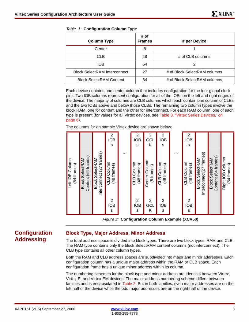
Virtex Series Configuration Architecture User GuideR13
Virtex Major Addresses
The CLB address space begins with rsquo0rsquo for the center column and alternates between the rightand left halves of the device for all the CLB columns then IOB columns and finally blockSelectRAM interconnect columns
The RAM address space has lsquo0rsquo for the left block SelectRAM content column and lsquo1rsquo for theright column
A XCV50 is shown in Figure 4 The shaded columns are in the RAM address space
Virtex-EM Major Addresses
The Virtex-EM family has the same numbering as the Virtex family but the block SelectRAMcontent columns begin with 1
Virtex-E Major Addresses
The Virtex-E family has block SelectRAM interspersed between CLB columns Both the CLBand RAM major addressing have been changed to allow for this
The CLB address space again begins with lsquo0rsquo for the center column and alternates between theright and left sides of the device for CLB columns and block SelectRAM interconnect columnsand finally IOB columns The difference is that in Virtex-E devices the block SelectRAM
Table 2 Major Addressing Scheme by Family
Column Type Block Type Virtex Virtex-E Virtex-EM
First MJA CLB 0 0 0
RAM 0 1 1
MJA Order CLB 1 Center2 CLB3 IOB4 BRAM Interconnect
1 Center2 CLB BRAM Interconnect3 IOB
1 Center2 CLB3 IOB4 BRAM Interconnect
RAM BRAM Content BRAM Content BRAM Content
2IOBs
2IOBs
2GCL
K
2IOBs
2IOBs
Left
IOB
Col
umn
(54
fram
es)
Blo
ck S
elec
tRA
MC
onte
nt (
64 fr
ames
)
Blo
ck S
elec
tRA
MIn
terc
onne
ct (
27 fr
ames
)
CLB
Col
umn
(48
fram
es)
hellip
CLB
Col
umn
(48
fram
es)
Cen
ter
Col
umn
(8 fr
ames
)
CLB
Col
umn
(48
fram
es)
hellip
CLB
Col
umn
(48
fram
es)
Blo
ck S
elec
tRA
MIn
terc
onne
ct (
27 fr
ames
)B
lock
Sel
ectR
AM
Con
tent
(64
fram
es
Rig
ht IO
B C
olum
n(5
4 fr
ames
)
2IOBs
2IOBs
2GCL
K
2IOBs
2IOBs
IOLe
ft
RA
M0
BIC
0
C1
C12
Cen
ter
C13
C24
BIC
1
RA
M1
IOR
ight
MA 26 0 28 24 2 0 1 23 27 1 25
Figure 4 Virtex Family Allocation of Frames to Device Resources (XCV50)
4 wwwxilinxcom XAPP151 (v15) September 27 20001-800-255-7778
Virtex Series Configuration Architecture User GuideR13
interconnect appear in the middle of the CLB addresses while in the Virtex and Virtex-EMfamilies they appear at the very end after the IOB columns Also note that the blockSelectRAM content columns begin with lsquo1rsquo (Virtex devices begin with lsquo0rsquo)
A XCV50E is shown in Figure 5 The shaded columns are in the RAM address space
Frames Frames are read and written sequentially with ascending addresses for each operationMultiple consecutive frames can be read or written with a single configuration command Thesmallest amount of data that can be read or written with a single command is a single frameThe entire CLB array plus the IOBs and block SelectRAM interconnect can be read or writtenwith a single command Each block SelectRAM Content must be read or written separately
Frame SizesFrame size depends on the number of rows in the device The number of configuration bits ina frame is 18 times ( CLB_rows+2) and is padded with zeroes on the right (bottom) to fit in 32-bitwords See Frame Organization on page 6 An additional padding word is needed at the endof each frame for pipelining Table 3 shows the frame sizes for all Virtex devices This table alsoshows the size in words of the bitstream for the CLB address space and the number of wordsin each RAM block
2IOB
s
2IOB
s
2IOB
s
2IOB
s
2GCLK
2IOB
s
2IOB
s
Blo
ck S
elec
tRA
MIn
terc
on
ne
ct(2
7 f
ram
es)
2IOB
s
2IOB
s
Blo
ck S
elec
tRA
MC
onte
nt (
64 fr
ames
)
Left
IOB
Col
umn
(54
fram
es)
Blo
ck S
elec
tRA
MC
onte
nt (
64 fr
ames
)B
lock
Sel
ectR
AM
Inte
rco
nn
ect(2
7 f
ram
es)
CLB
Col
umn
(48
fram
es)
hellipC
LB C
olum
n(4
8 fr
ames
)B
lock
Sel
ectR
AM
Con
tent
(64
fram
es)
Blo
ck S
elec
tRA
MIn
terc
on
ne
ct(2
7 f
ram
es)
CLB
Col
umn
(48
fram
es)
hellip
CLB
Col
umn
(48
fram
es)
Cen
ter
Col
umn
(8 fr
ames
)C
LB C
olum
n(4
8 fr
ames
)
hellip
CLB
Col
umn
(48
fram
es)
Blo
ck S
elec
tRA
MC
onte
nt (
64 fr
ames
)C
LB C
olum
n(4
8 fr
ames
)
hellip
CLB
Col
umn
(48
fram
es)
Blo
ck S
elec
tRA
MIn
terc
on
ne
ct(2
7 f
ram
es)
Rig
ht IO
B C
olum
n(5
4 fr
ames
)
2IOB
s
2IOB
s
2IOB
s
2IOB
s
2GCLK
2IOB
s
2IOB
s
2IOB
s
2IOB
s
IOLe
ft
RA
M0
BIC
0
C1
C6
RA
M1
BIC
1
C7
C12
Cen
ter
C13
CLB
18
BIC
2
RA
M2
C19
C24
BIC
3
RA
M3
IOR
ight
MA
30 4 28 26 16 2 14 12 2 0 1 11 13 1 15 25 27 3 29
Figure 5 Virtex-E Family Allocation of Frames to Device Resources (XCV50E)
XAPP151 (v15) September 27 2000 wwwxilinxcom 51-800-255-7778
Virtex Series Configuration Architecture User GuideR13
Frame OrganizationEach frame sits vertically in the device with the ldquofrontrdquo of the frame at the top As shown inFigure 6 it is convenient to consider the frame horizontally when it is viewed as part of abitstream The top IOBs are shown on the left followed by the CLBs in the column and thebottom IOBs on the right Bits in frames are allocated as follows
For CLB columns the first 18 bits control the two IOBs at the top of the column then 18 bits areallocated for each CLB row finally the next 18 bits control the two IOBs at the bottom of the
Table 3 Virtex Series Devices
Device Row times ColBits
FrameWordsFrame
Virtex Virtex-E
RAMCols
of 32-bit Read-backWords (1)
RAMCols
RAMSpace
of 32-bit Read-backWords (1)
CLB(all)
RAM(1 col)
CLB(all)
RAM(1 col)
XCV50 16 times 24 384 12 2 15876 780 - - - -
XCV50E 16 times 24 384 12 - - - 4 6 16524 780
XCV100 20 times 30 448 14 2 22554 910 - - - -
XCV100E 20 times 30 448 14 - - - 4 12 23310 910
XCV150 24 times 36 512 16 2 30384 1040 - - - -
XCV200 28 times 42 576 18 2 39366 1170 - - - -
XCV200E 28 times 42 576 18 - - - 4 12 40338 1170
XCV300 32 times 48 672 21 2 51975 1365 - - - -
XCV300E 32 times 48 672 21 - - - 4 12 53109 1365
XCV400 40 times 60 800 25 2 76275 1625 - - - -
XCV400E 40 times 60 800 25 - - - 4 12 77625 1625
XCV405E 40 times 60 800 25 - - - 14 4 84375 1625
XCV600 48 times 72 960 30 2 108810 1950 - - - -
XCV600E 48 times 72 960 30 - - - 6 12 112050 1950
XCV800 56 times 84 1088 34 2 142902 2210 - - - -
XCV812E 56 times 84 1088 34 - - - 20 4 159426 2210
XCV1000 64 times 96 1248 39 2 186381 2535 - - - -
XCV1000E 64 times 96 1248 39 - - - 6 12 190593 2535
XCV1600E 72 times 108 1376 43 - - - 8 12 237231 2795
XCV2000E 80 times 120 1536 48 - - - 8 12 292464 3120
XCV2600E 92 times 138 1728 54 - - - 8 12 375678 3510
XCV3200E 104 times 156 1952 61 - - - 8 12 477081 3965
Notes1 Includes pad frame in calculation
6 wwwxilinxcom XAPP151 (v15) September 27 20001-800-255-7778
Virtex Series Configuration Architecture User GuideR13
CLB column The frame then contains enough ldquopadrdquo bits to make it an integral multiple of 32bits
For IOB columns the frame allocates 18 bits per three IOB rows Figure 7 When reading andwriting frames bits are grouped into 32-bit words starting on the left (corresponding to the topof the device) If the last word does not completely fill a 32-bit word it is padded on the right withzeroes
For block SelectRAM content columns (Figure 8) the first 18 bits are pad bits then 72 bits areallocated for each RAM row finally there are another 18 pad bits The frame then adds enoughldquopadrdquo bits to make it an integral multiple of 32 bits
Location of LUT SelectRAM BitsWith respect to the beginning of a configuration frame relative locations of LUT SelectRAM bitswithin the bitstream are the same for every CLB slice The bits of a LUT SelectRAM are spreadacross 16 consecutive frame Minor Addresses Each frame Minor Address contains allinstances of a single bit index for that column These 16 frames contain all 16 bits of the LUTSelectRAM for a column of CLB slices You must read or write the 16 frames containing thosebits to read or write the entire LUT SelectRAM
Figure 6 CLB Column Frame Organization
Figure 7 IOB Column Frame Organization
Figure 8 Block SelectRAM Content Column Frame Organization
Note LUT SelectRAM bits are stored inverted Flip-Flop data are stored in their true senseWhen reading or writing LUT SelectRAM data from the bitstream it is negated from the logicsense of the data For example a 4-input AND gate has the truth tableLUT[150] = 1000000000000000
This truth table isstored internally in theLUTSelectRAMasLUT[150] = 0111111111111111Ofcourse user logic reading the data from the LUT SelectRAM would read the correct logicvalue LUT[150] = 1000000000000000
Top 2 IOBs13 Bottom 2 IOBs1313
CLB Rn1313
13 18131813181318131813
CLB R213CLB R113
x151_06_020700
Top 3 IOBs Bottom 3 IOBs1313
181818
3 IOBs
x151_07_020800
Pad PadRAM Rn
1872727218
RAM R1RAM R0
x151_08_021800
XAPP151 (v15) September 27 2000 wwwxilinxcom 71-800-255-7778
Virtex Series Configuration Architecture User GuideR13
ConfigurationData Operations
Reading Configuration DataConfiguration information can be read from the Virtex devices if readback is enabled in thecurrent configuration (See the description of the Control Register field SBITS on page 21)CLB and IOB configuration data can be read while the device is operating
When reading data from a Virtex device a pad frame is read before any of the data framesThis is in addition to the pad word in each data frame The pad frame must be included in theword count to be read from the device
Each frame read from the device consists of the number of words shown in Table 3
For example the XCV150 has 16-word frames When reading frames the first word of a frameis a pad word Including the pad frame the XCV150 has 1899 (3038416) frames (SeeFigure 9)
Writing Configuration DataConfiguration information can be written to a Virtex device while the device is running if writingis enabled in the current configuration (See the Control Register field SBITS in Table 23) Re-writing the same configuration data does not generate any transient signals
Changing configuration data may generate transient signals especially if LUT values or signalrouting is changed For this case all the logic cells and routing can be placed in a non-contentious state by asserting the GHIGH_B signal See the description for the CommandRegister (CMD) on page 18
When writing configuration data to the Virtex device whether from the SelectMAP or JTAGinterfaces the data frames are written to the device with each frame followed by a pad wordAfter all the data frames are written a pad frame must be written (to flush internal pipelines)The pad words and pad frame must be included in the number of words to be written to thedevice (Table 3)
For example the XCV1000 has 39-word frames When writing frames the last word of theframe is a pad word Including the pad frame the XCV1000 has 4779 (18638139) framesSee Figure 10)
Altering Configuration DataVirtex devices support the Read-Modify-Write (RMW) method of changing LUT SelectRAMdata Therefore it is possible to read or alter the contents of one or more LUT SelectRAMsthrough the JTAG or SelectMAP interfaces When writing data to one or more LUTSelectRAMs all the bits in the frame must have valid configuration information This can beassured by altering valid configurations from bitstream files or from frames read from a properlyconfigured Virtex device When using the RMW method it may be expeditious to read the dataignoring the pad frame and the pad word of only the first frame This aligns the remaining
Pad Frame (16 words)Pad Word Data Frame 0 (15 words)
hellip
hellip
Pad Word Data Frame n (15 words)
Figure 9 XCV150 Frame Padding for Device Read
Data Frame 0 (38 words) Pad Word
hellip
Data Frame n (38 words) Pad WordPad Frame (39 words)
Figure 10 XCV1000 Frame Padding for Device Write
8 wwwxilinxcom XAPP151 (v15) September 27 20001-800-255-7778
Virtex Series Configuration Architecture User GuideR13
configuration data in the Device Write format After modifying the configuration the altered datacan be written to the Virtex device followed by a pad word and a pad frame
It is not necessary to retain the contents of the pad frame or pad words However pad wordsand pad frames are included in the CRC calculation
Definitions Two sets of variables are defined to determine where a desired bit is in the configuration dataThe first is a set of ldquoindependentrdquo variables or design attributes namely characteristics of thedesign that are known ie the device size and which CLB and bit(s) within the CLB to locateTable 4 The second set is a set of ldquodependentrdquo variables or design variables namely valuesthat must be calculated to find the bit(s) of interest listed in Table 5
Note Frames span an entire column of CLB slices (or IOBs) Thus when changing LUTSelectRAM bit 0 for a single CLB slice (eg R3C4S1) LUT SelectRAM bit 0 for all slices inthat column (ie RC4S1) is written with the same command One must ensure that either allother data in the slice is constant or changed externally through partial configurations
LUT SelectRAMs not configured externally should not lie in the same slice with LUTs or LUTSelectRAMs that are re-configured externally Such a mixture can cause the unrelated LUTSelectRAM data to be re-configured when the frames are written to the device Figure 11shows what can happen if this restriction is not observed
In this example it is the objective to perform a Read-Modify-Write on the LUT SelectRAM inR2C3S1 in column 3 which is shown in the first column in the figure Row 2 contains a LUTcontaining the value AB Row 3 contains a SelectRAM containing the value C3 Because theRead and Write operations operate on an entire frame the RAM in R3C3S1 is also read andwritten when R2C3S1 is read and written Performing the Readback operation reads all theLUT and SelectRAM values for the column Before the new value for the LUT is written it ispossible for the on-chip circuitry to write a new value such as 14 into the SelectRAM Whenthe new value BD is written via the configuration interface into LUT R2C3S1 the value C3 isalso written into RAM R3C3S1 This may not always be desirable (It is design-dependent)
Figure 11 Potential Write Conflicts
x151_11_020800
LUT R2C3S113AB13
RAM R3C3S113C313
Before13Readback
13
LUT R2C3S113AB13
RAM R3C3S1131413
Before13Configuration 13
Write
13
LUT R2C3S113BD13
RAM R3C3S113C313
After13Configuration13
Write
13
Table 4 Design Attributes (Independent Variables)
Term Definition
Chip_Cols of CLB columns on the Virtex device
Chip_Rows of CLB rows on the Virtex device
Chip_Rams of block SelectRAM columns on the Virtex device
RAM_Space Spacing of block SelectRAM columns (in terms of CLB columns)
FL of 32-bit words in the frame
XAPP151 (v15) September 27 2000 wwwxilinxcom 91-800-255-7778
Virtex Series Configuration Architecture User GuideR13
RW 1 for Read 0 for Write
CLB_Col Column number of the desired CLB
CLB_Row Row number of the desired CLB
Slice 0 or 1
FG 0 for the F-LUT 1 for the G-LUT
lut_bit The desired bit from the given LUT Bits in the LUT are indexed from 0 to 15
XY 0 for the X Flip-Flop 1 for the Y Flip-Flop
RAM_Col Column number of the desired block SelectRAM
RAM_Row Row number of the desired block SelectRAM
ram_bit The desired bit from the given block SelectRAM Bits are indexed from 0 to4095
Table 5 Design Variables (Dependent Variables)
Term Definition
MJA Frame Major Address
MNA Frame Minor Address
fm_st_wd The index of the word within a full configuration segment that correspondsto the starting word of the desired frame A full configuration segment isdefined as the following 1) for CLBIOB all CLB IOB and RAMinterconnect frames beginning at MJA=0 MNA=0 and 2) for blockSelectRAM all RAM content frames for the given RAM column Words arenumbered starting at 0
fm_wd The index of the 32-bit word within a frame that contains the desired bitWords in a frame are numbered starting at 0
fm_wd_bit_idx The bit index of the desired bit within frame word fm_wd Words areindexed in ldquobig-endianrdquo style with bit 31 on the left and bit 0 on the right
fm_bit_idx Bit index within a frame of the desired bit Numbered starting with 0 as theleft-most (first) bit Bit numbering within a frame continues across all thewords in the frame
Table 6 Functions used in Equations
Functions Definition
floor(x) The largest integer not larger than x Eg floor(31) = 3 because the nextlargest integer 4 is larger than 31 floor(3)=3
ceiling(x) The smallest integer greater than or equal to x For example ceiling(32) = 4because 4 is greater than 32 and 3 is not ceiling (4) = 4
The modulus operation 5 2 = 1 5 3 = 2 5 5 = 0
Table 4 Design Attributes (Independent Variables) (Continued)
Term Definition
10 wwwxilinxcom XAPP151 (v15) September 27 20001-800-255-7778
Virtex Series Configuration Architecture User GuideR13
CLB LUTSelectRAMDependentVariables
Table 7 shows equations for the LUT SelectRAM ldquoDependent Variablesrdquo that were defined inTable 5
Virtex-E CLB LUT SelectRAM Dependent VariablesThe additional block SelectRAM columns in Virtex-E devices require an adjustment to the MJAThe following equations calculate the adjustment necessary for each of the affected dependentvariables For each variable calculate the base value based upon the Virtex equations onlyand then add the resulting Virtex adjustment
The left and right sides of the device are treated differently
LUT SelectRAM ExamplesSee ldquoExamplesrdquo on page 27 for several examples of reading and evaluating configuration dataThe examples illustrate how to make use of these equations to find the desired data in abitstream
Table 7 Virtex Equations for LUT SelectRAM Dependent Variables
Term Definition
MJA if (CLB_Col le Chip_Cols2)then Chip_Cols ndash CLB_Col times 2 + 2else 2 times CLB_Col ndash Chip_Cols ndash 1
MNA lut_bit + 32 ndash Slice times (2 times lut_bit + 17)
fm_bit_idx 3 + 18 times CLB_Row ndash FG + RW times 32
fm_st_wd FL times (8 + (MJA ndash1) times 48 + MNA) + RW times FL
fm_wd floor(fm_bit_idx32)
fm_wd_bit_idx 31 + 32 times fm_wd ndash fm_bit_idx
Notes
bull Do NOT input the final results back into the original Virtex equations (eg do not useMJAfinal value to calculate fm_st_wd)
bull MJAfinal = MJA + MJA_adj
bull fm_st_wdfinal = fm_st_wd + fm_st_wd_adj
Table 8 CLB Location
CLB Location CLB Column
Left CLB_Col le Chip_Cols2
Right CLB_Col gt Chip_Cols2
Table 9 Virtex-E Families Adjustments for LUT SelectRAM Dependent Variables
Term Definition
MJA_adj Left RAM_Bound = (Chip_Rams2 - 1) x RAM_SpaceMJA_adj = 2 x ceiling((RAM_Bound - CLB_Col + 1) RAM_Space)
Right
RAM_Bound = Chip_Cols - (Chip_Rams2 - 1) x RAM_Space + 1MJA_adj = 2 x ceiling((CLB_Col - RAM_Bound + 1) RAM_Space)
fm_st_wd_adj FL times (27 x MJA_adj)
XAPP151 (v15) September 27 2000 wwwxilinxcom 111-800-255-7778
Virtex Series Configuration Architecture User GuideR13
CLB Flip-FlopDependentVariables
Equations for the CLB flip-flops can be found in Table 10 Their locations are calculatedsimilarly to the LUT SelectRAM locations Equations for the CLB FF Dependent Variables aredefined in Table 5
Virtex-E CLB Flip-Flop Dependent VariablesApply the adjustments given in Table 8 and Table 9
IOB DependentVariables
Each IOB contains four values that can be captured into special registers These values are
bull I mdash the input flip-flop
bull O mdash the output flip-flop
bull T mdash the flip-flop for the tri-state control
bull P mdash the value of the IO pad
These values are captured by utilizing the CAPTURE_VIRTEX symbol in your design TheLibraries Guide has more details on the use of this symbol The following registers will be readas part of the readback data
Access to the IOB flip-flops is different for the top and bottom IOBs versus the left and rightIOBs
The top and bottom IOBs are part of the CLB column frames There are two IOBs at the top andbottom of each CLB column
The left and right IOBs are in columns by themselves There are three IOBs per CLB row
IOBs are numbered clockwise around the die Pad 1 is located at the left side of the top edgeabove CLB column 1 The equations for where to find IOB flip-flops in the bitstream are basedon the pad number which is the same for a given size device not the package pin name whichvaries from package to package The mapping from package pin names to pad numbers canbe found in EPIC or fpga_editor
Table 11 contains the numeric pad indices for the pads on all four edges of the device in termsof the number of CLB columns and rows on the device
Table 10 Virtex Equations for CLB FF Dependent Variables
Term Definition
MJA if (CLB_Col le Chip_Cols2)then Chip_Cols ndash CLB_Col times 2 + 2else 2 times CLB_Col ndash Chip_Cols ndash 1
MNA Slice times (12 times XY ndash 43) ndash 6 times XY + 45
fm_bit_idx (18 times CLB_Row) + 1 + (32 times RW)
fm_st_wd FL times (8 + (MJA ndash1) times 48 + MNA) + RW times FL
fm_wd floor(fm_bit_idx32)
fm_wd_bit_idx 31 + 32 times fm_wd ndash fm_bit_idx
12 wwwxilinxcom XAPP151 (v15) September 27 20001-800-255-7778
Virtex Series Configuration Architecture User GuideR13
Table 12 shows the equations for the dependent variables for the IOB flip-flops The variable iin this table refers to the index of pad i
Table 11 IOB Pad Indices
PadLocation Pad Index i
Top 1 le i le Chip_Cols times 2
Right Chip_Cols times 2 +1 le i le Chip_Cols times 2 + Chip_Rows times 3
Bottom Chip_Cols times 2 + Chip_Rows times 3 + 1 le i le Chip_Cols times 4 + Chip_Rows times 3
Left Chip_Cols times 4 + Chip_Rows times 3 + 1 le i le Chip_Cols times 4 + Chip_Rows times 6
Table 12 Equations for IOB Dependent Variables
Term Definition
MJA
Topif (i le Chip_Cols)then Chip_Cols ndash ceiling(i2) times 2 + 2else 2 times ceiling (i2) ndash Chip_Cols ndash1
Right Chip_Cols + 1
Bottomif (i gt 3 times (Chip_Cols + Chip_Rows))then 2 times ceiling((i ndash 3 times Chip_Cols ndash 3 times Chip_Rows)2)else Chip_Cols ndash 2 times floor((i ndash 2 times Chip_Cols ndash 3 times Chip_Rows ndash 1)2) ndash 1
Left Chip_Cols + 2
MNA
Top
I ndash 25 times (i2) + 45
O ndash 13 times (i2) + 39
T ndash 5 times (i2) + 35
P ndash 4 times (i2) + 25
Right
I t = (i ndash 2 times Chip_Cols) 3 MNA = 275 times t2 ndash 575 times t + 32
O t = (i ndash 2 times Chip_Cols) 3 MNA = 215 times t2 ndash 515 times t + 38
T t = (i ndash 2 times Chip_Cols) 3 MNA = 175 times t2 ndash 475 times t + 42
P 50
Bottom
I 25 times ((i ndash 2 x Chip_Cols - 3 x Chip_Rows)2) + 20
O 13 times ((i ndash 2 x Chip_Cols - 3 x Chip_Rows)2) + 26
T 5 times ((i ndash 2 x Chip_Cols - 3 x Chip_Rows)2) + 30
P 4 times ((i ndash 2 x Chip_Cols - 3 x Chip_Rows)2) + 21
Left
I t = (i ndash 4 x Chip_Cols - 3 x Chip_Rows)3 MNA = 175 times t2 ndash 475 times t + 45
O t = (i ndash 4 x Chip_Cols - 3 x Chip_Rows)3 MNA = 235 times t2 ndash 535 times t + 39
T t = (i ndash 4 x Chip_Cols - 3 x Chip_Rows)3 MNA = 275 times t2 ndash 575 times t + 35
P 50
XAPP151 (v15) September 27 2000 wwwxilinxcom 131-800-255-7778
Virtex Series Configuration Architecture User GuideR13
Virtex-E IOB Dependent VariablesSimilar to CLB dependent variables only the variables affected by the major address aredifferent in Virtex-E and Virtex-EM devices versus Virtex devices A simple way to account forthe change is to determine the CLB column where the pad resides (only true for top andbottom) Then the adjustment calculated for the CLB column can be applied The conversionto CLB columns is found in Table 13
fm_bit_idx
Top 32 times RW
Right
I O ampT 18 times (1 + floor ((i ndash 2 times Chip_Cols ndash 1)3)) + 32 times RW
Pt = (i ndash 2 times Chip_Cols) 3fm_bit_idx = 18 times (1 + floor ((i ndash 2 times Chip_Cols ndash 1)3)) + 6 times t2 ndash 17 times t + 15 + 32 timesRW
Bottom 18 times (Chip_Rows + 1)+ 32 times RW
Left
I O ampT18 times (Chip_Rows ndash floor((i ndash 4 times Chip_Cols ndash 3 times Chip_Rows ndash 1)3)) + 32 times RW
Pt = (i ndash 4 times Chip_Cols ndash 3 times Chip_Rows)3fm_bit_idx = 18 times (Chip_Rows ndash floor ((i ndash 4 times Chip_Cols ndash 3 times Chip_Rows ndash 1)3))ndash 105 times t2 + 215 times t + 4 + 32 times RW
fm_st_wdif (MJA gt Chip_Cols + 1)then FL times (54 times MJA ndash 46 + MNA ndash 6 times Chip_Cols) + RW times FLelse FL times (8 + (MJA ndash1) times 48 + MNA) + RW times FL
fm_wd floor (fm_bit_idx32)
fm_wd_bit_idx 31 + 32 times fm_wd ndash fm_bit_idx
Table 12 Equations for IOB Dependent Variables (Continued)
Term Definition
Table 13 Pad -gt CLB Column
Term Definition
CLB_ColTop ceiling(i2)
Bottom ceiling((4 x Chip_Cols + 3 x Chip_Rows + 1 - i)2)
Table 14 Virtex-E Families Adjustments for IOB Dependent Variables
Term Definition
MJA_adj
Top use Table 8 and Table 9
Right Chip_Rams
Bottom use Table 8 and Table 9
Left Chip_Rams
fm_st_wd_adj FL times (27 x MJA_adj)
14 wwwxilinxcom XAPP151 (v15) September 27 20001-800-255-7778
Virtex Series Configuration Architecture User GuideR13
BlockSelectRAMDependentVariables
The equations for the block SelectRAM dependent variables are given in Table 15 Therelationship of a particular memory cell index in the context of a given configuration is describedin XAPP130 ldquoUsing the Vir tex Bloc k SelectRAM+ Resour cerdquo
Virtex-E Block SelectRAM Dependent VariablesThe RAM major address numbering scheme changed slightly such that the lowest MJA on theleft side is now 2 instead of 0 As in the case for the CLB equations the adjustments belowshould be applied after the Virtex equations
Table 15 Virtex Equations for Block SelectRAM Dependent Variables
Term Definition
MJAif (RAM_Col lt Chip_Rams2)then 2 x (Chip_Rams2 - 1 - RAM_Col)else 2 x (RAM_Col - Chip_Rams2) + 1
MNA
1 x floor(((ram_bit 64) 64)32) + 2 x floor(((ram_bit 64) 32)16)+ 4 x floor(((ram_bit 64) 16)8) + 8 x floor(((ram_bit 64) 8)4)+ 16 x floor(((ram_bit 64) 4)2) + 32 x floor(((ram_bit 64) 2)1)equivalent to MNA = div64[05] where div64[50] = floor(ram_bit64)
fm_bit_idxobtain value for bitpos from Table 16
fm_bit_idx = 18 + 72 x RAM_Row + bitpos
fm_st_wd FL times MNA + RW times FL
fm_wd floor(fm_bit_idx32)
fm_wd_bit_idx 31 + 32 times fm_wd ndash fm_bit_idx
Table 16 Virtex Block SelectRAM Bit Position Within a Given Block SelectRAM
ram
_bit
6
4
bitp
os
ram
_bit
6
4
bitp
os
ram
_bit
6
4
bitp
os
ram
_bit
6
4
bitp
os
ram
_bit
6
4
bitp
os
ram
_bit
6
4
bitp
os
ram
_bit
6
4
bitp
os
ram
_bit
6
4
bitp
os
0 42 8 45 16 29 24 26 32 43 40 44 48 28 56 27
1 58 9 61 17 13 25 10 33 59 41 60 49 12 57 11
2 41 10 46 18 30 26 25 34 40 42 47 50 31 58 24
3 57 11 62 19 14 27 9 35 56 43 63 51 15 59 8
4 50 12 53 20 21 28 18 36 51 44 52 52 20 60 19
5 49 13 54 21 22 29 17 37 48 45 55 53 23 61 16
6 66 14 69 22 5 30 2 38 67 46 68 54 4 62 3
7 65 15 70 23 6 31 1 39 64 47 71 55 7 63 0
Table 17 Virtex-E and Virtex-EM Adjustments for Block SelectRAM DependentVariables
Term Definition
MJA_adj if (RAM_Col lt Chip_Rams2) MJA_adj = 2
XAPP151 (v15) September 27 2000 wwwxilinxcom 151-800-255-7778
Virtex Series Configuration Architecture User GuideR13
ConfigurationLogic Basics
Configuration DataConfiguration data is organized as 32-bit words There are two major commands that theconfiguration data can contain Read and Write A configuration command is executed whenthe configuration command is read or written to the appropriate command register
The OP field contains 01 for a Read operation and 10 for a Write operation (See Figure 12)
A command is organized as a packet with a header word and optional data words The headerword is the first word written to the appropriate command register for a read or write operationThe header word contains a type field (001) an operand field a register address field and aword count field The format for the command header is shown in Figure 13 on page 17
The Register Address field defines the target of this command as defined in Table 18 on page17
The header word count field contains an integer between 0 and 2047 and indicates thenumber of words that follow the header Larger word counts (between 2048 and 1048575words) are achieved by setting the header word count to 0 The Extension header word has atype field = 010 an OP field that must match the OP field in the preceding Command Headerword and a 20-bit word count this format is shown Figure 14 on page 17
Configuration FlowVirtex devices are configured by presenting configuration data to the SelectMAP or JTAGinterfaces in a specific sequence
For Initial Configuration
1 Issue one or more pad words (SelectMAP only)
2 Issue Sync word (SelectMAP only)
3 Reset CRC
4 Set FLR
5 Set COR
6 Set MASK
7 Set CTL (Set PERSIST if you want to keep SelectMAP active after this configuration)
8 Issue a SWITCH (switch CCLK frequency) command to the CMD register This isnecessary only in Master Serial configuration mode
Reading Configuration
These commands can be issued to read a full configuration or for a partial configuration afterthe device has been completely configured
1 Issue a Sync word (SelectMAP only) if the previous configuration command was aborted
2 Set the FAR to the starting address
3 Issue a RCFG (read configuration) command to the CMD register
4 Write the number of words to be read to the FDRO register
5 Flush the command pipeline with a pad word
6 Read data frames
OP CODERead 01Write 10
Figure 12 OP Field Code
16 wwwxilinxcom XAPP151 (v15) September 27 20001-800-255-7778
Virtex Series Configuration Architecture User GuideR13
Writing Configuration
These commands can be issued either as part of an initial configuration or for a partialconfiguration after the device has been configured
1 Issue a Sync word (SelectMAP only) if the previous configuration command was aborted
2 If the frames being written can cause contention then assert the GHIGH_B signal
3 Set the FAR to the starting address
4 Issue a WCFG (write configuration) command to the CMD register
5 Write the number of words to be written to the FDRI register
6 Write data frames
7 If the GHIGH_B signal was asserted de-assert it by writing the LFRM (Last Frame)command to the CMD register and write one pad frame
ConfigurationRegisters
Configuration logic is accessed and controlled via a collection of 32-bit registers called theconfiguration registers (see Table 18) Registers are described in the following sections
Type OP Register Address RSV Word Count31 30 29 28 27 26 25 24 23 22 21 20 19 18 17 16 15 14 13 12 11 10 9 8 7 6 5 4 3 2 1 00 0 1 x x 0 0 0 0 0 0 0 0 0 0 x x x x 0 0 x x x x x x x x x x x
Notes1 Locations within fields containing a zero or one must have these values An X in a bit field indicates that the value is variable and must
be set2 Heavy vertical lines are used to separate fields Light vertical lines separate nibbles in the word
Figure 13 Command Header Format
Type OP Word Count31 30 29 28 27 26 25 24 23 22 21 20 19 18 17 16 15 14 13 12 11 10 9 8 7 6 5 4 3 2 1 00 1 0 x x 0 0 0 0 0 0 0 x x x x x x x x x x x x x x x x x x x x
Notes1 Locations within fields containing a zero or one must have these values An X in a bit field indicates that the value is variable and must
be set2 Heavy vertical lines are used to separate fields Light vertical lines separate nibbles in the word
Figure 14 Large Block Count Header Extension Format
Table 18 Configuration Register Addresses
Register Name Mnemonic RW Binary Address
CRC CRC RW 0000
Frame Address FAR RW 0001
Frame Data Input FDRI W 0010
Frame Data Output FDRO R 0011
Command CMD RW 0100
Control CTL RW 0101
Control Mask MASK RW 0110
Status STAT R 0111
Legacy Output LOUT W 1000
XAPP151 (v15) September 27 2000 wwwxilinxcom 171-800-255-7778
Virtex Series Configuration Architecture User GuideR13
Command Register (CMD)The content of the Command Register (CMD) is interpreted by the configuration state machineConfiguration commands control the operation of the configuration state machine the FrameData Register (FDR) and some of the global signals The command in the Command Registeris executed each time the FAR is loaded with a new value The effect of each command isdefined in Table 19
Configuration Option COR RW 1001
Reserved mdash mdash 1010
Frame Length FLR RW 1011
Reserved mdash mdash 1100
Reserved mdash mdash 1101
Reserved mdash mdash 1110
Reserved mdash mdash 1111
Table 18 Configuration Register Addresses (Continued)
Register Name Mnemonic RW Binary Address
Table 19 Configuration Commands
Cmd Code Description
Rsvd 0000 Reserved
WCFG 0001Write Configuration Data mdash Used prior to writing configuration data to the FDRI It takes theinternal configuration state machine through a sequence of states that control the shifting of the FDRand the writing of the configuration memory (See Frame Data Input Register (FDRI) on page 24)
Rsvd 0010 Reserved
LFRM 0011Last Frame mdash This command is loaded prior to writing the last (pad) data frame if the GHIGH_Bsignal was asserted This command is not necessary if the GHIGH_B signal was not asserted Thisallows overlap of the last frame write with the release of the GHIGH_B signal
RCFG 0100Read Configuration Data mdash Used prior to reading frame data from the FDRO Similar to the WCFGcommand in its effect on the FDR (see Frame Data Output Register (FDRO) on page 24)
START 0101Begin Startup Sequence mdash Starts the startup sequence This command is also used to start ashutdown sequence prior to partial re-configuration The Startup Sequence begins with the nextsuccessful CRC check (see Cyclic Redundancy Check (CRC) on page 22)
RCAP 0110Reset Capture mdash Used when performing capture in single-shot mode This command must be usedto reset the capture signal if single-shot capture has been selected
RCRC 0111 Reset CRC mdash Used to reset CRC register (see Cyclic Redundancy Check (CRC) on page 22)
AGHIGH 1000Assert GHIGH_B Signal mdash Used prior to re-configuration to prevent contention while writing newconfiguration data All CLB outputs and signals are forced to a one
SWITCH 1001Switch CCLK Frequency mdash Used to change (increase) the frequency of the Master CCLK Thenew frequency is specified in Table 21
Rsvd 1010 Reserved
Rsvd 1011 Reserved
Rsvd 1100 Reserved
18 wwwxilinxcom XAPP151 (v15) September 27 20001-800-255-7778
Virtex Series Configuration Architecture User GuideR13
Configuration Option Register (COR)The Configuration Option Register (COR) is used to select configuration options that areillustrated in Figure 15 and defined in Table 20 Entries in this table are further explained in thefollowing tables
Rsvd 1101 Reserved
Rsvd 1110 Reserved
Rsvd 1111 Reserved
Table 19 Configuration Commands (Continued)
Cmd Code Description
DO
NE
_PIP
E
DR
IVE
_DO
NE
SIN
GLE
OS
CF
SE
L
SS
CLK
SR
C
LOC
K_W
AIT
SH
UT
DO
WN
DO
NE
_CY
CLE
LCK
_CY
CLE
GT
S_C
YC
LE
GW
E_C
YC
LE
GS
R_C
YC
LE
31 30 29 28 27 26 25 24 23 22 21 20 19 18 17 16 15 14 13 12 11 10 9 8 7 6 5 4 3 2 1 00 x x x x x x x x x x x x x x x x x x x x x x x x x x x x x x x
Notes1 Locations within fields containing a zero or one must have these values An X in a bit field indicates that the value is variable and must
be set2 Heavy vertical lines are used to separate fields Light vertical lines separate nibbles in the word
Figure 15 COR (Configuration of Option Register) Fields
XAPP151 (v15) September 27 2000 wwwxilinxcom 191-800-255-7778
Virtex Series Configuration Architecture User GuideR13
Table 21 shows the allowed values for the OSCFSEL field of the COR Setting OSCFSEL toone of these values will set the Master CCLK frequency to the specified value
Table 20 Configuration Option Register Fields
Field Bit Indices DescriptionBitgenDefault
DONE_PIPE 30
0 No pipeline stage for DONEIN
1 Add pipeline stage to DONEINFPGA waits on DONE that is delayed by one (1) cycle of the StartupClkrather than the pin itself Use this option when StartupClk is running at highspeeds
0
DRIVE_DONE 290 DONE pin is open drain
1 DONE pin is actively driven high0
SINGLE 28 Readback capture is one-shot 0
OSCFSEL 2722 Select CCLK frequency in Master Serial configuration mode 2
SSCLKSRC 2120
Startup sequence clock source00 Cclk01 UserClk1x JTAGClk
0
LOCK_WAIT 1916
4-bit mask indicating which DLL lock signals to wait for during LCK cycleThe 4 bits (from MSB to LSB) correspond to DLLs TL=3 TR=2 BL=1BR=0 (top-left top-right etc) In Virtex-E devices where there are 8 DLLseach mask bit applies to the 2 DLLs in that quadrant of the device Thedefault is not to wait for any DLL lock signals
0
SHUTDOWN 15
Indicate whether doing a startup or shutdown sequence
0 Startup
1 Shutdown sequence
0
DONE_CYCLE 1412 Startup phase in which DONE pin is released 3
LCK_CYCLE 119 Stall in this startup phase until DLL locks are asserted 7
GTS_CYCLE 86 Startup phase in which IOs switch from tri-state to user design 4
GWE_CYCLE 53 Startup phase in which the global write-enable is asserted 5
GSR_CYCLE 20 Startup phase in which the global setreset is negated 5
Table 21 OSCFSEL-Specified Master CCLK Frequencies)
CCLK(MHz) OSCFSEL
CCLK(MHz) OSCFSEL
CCLK(MHz) OSCFSEL
43 000010 13 001010 41 100111
54 010001 15 001101 45 110011
69 000100 20 010111 51 101010
81 000101 26 011010 55 110100
20 wwwxilinxcom XAPP151 (v15) September 27 20001-800-255-7778
Virtex Series Configuration Architecture User GuideR13
Table 22 shows the values of the DONE_CYCLE LCK_CYCLE GTS_CYCLE GWE_CYCLEand GSR_CYCLE fields in COR This table shows the step in the start-up sequence when eachof these signals becomes active
Control Register (CTL)The Control Register (CTL) fields are illustrated in Figure 16 on page 21 and defined inTable 23
92 000110 30 011101 60 101101
100 000111 34 110010 mdash mdash
Notes1 These values are accurate to +45 ndash 30
Table 22 COR Startup Cycle Fields
FieldValue
DONE_CYCLE(DONE Active)
GTS_CYCLE(GTS_CFGInactive)
GSR_CYCLE(GSR Inactive)
GWE_CYCLE(GWE Active) LCK_CYCLE
000 1 1 1 1 0
001 2 2 2 2 1
010 3 3 3 3 2
011 4 (default) 4 4 4 3
100 5 5 (default) 5 5 4
101 6 6 6 (default) 6 (default) 5
110 mdash DoneIndagger DoneIndagger DoneIndagger 6
111 Keep State Keep State Keep State Keep State Donrsquot Wait(default)
Notes1 dagger DONE if DonePipe = No else the delayed version of DONE
Table 21 OSCFSEL-Specified Master CCLK Frequencies) (Continued)
CCLK(MHz) OSCFSEL
CCLK(MHz) OSCFSEL
CCLK(MHz) OSCFSEL
SB
ITS
PE
RS
IST
GT
S_U
SR
_B
31 30 29 28 27 26 25 24 23 22 21 20 19 18 17 16 15 14 13 12 11 10 9 8 7 6 5 4 3 2 1 00 0 0 0 0 0 0 0 0 0 0 0 0 0 0 0 0 0 0 0 0 0 0 x x x 0 0 0 0 0 x
Notes1 Locations within fields containing a zero or one must have these values An X in a bit field indicates that the value is variable and must
be set2 Heavy vertical lines are used to separate fields Light vertical lines separate nibbles in the word
Figure 16 Control Register Fields
XAPP151 (v15) September 27 2000 wwwxilinxcom 211-800-255-7778
Virtex Series Configuration Architecture User GuideR13
Cyclic Redundancy Check (CRC)A data input error checking mechanism is provided through the Cyclic Redundancy Check(CRC) register When data is written to any configuration register (except LOUT) a 16-bit CRCvalue is calculated using both the register data and the address This value is saved in the CRCregister At the end of any series of writes a pre-calculated CRC block-check value may bewritten to the CRC register If the resulting value is non-zero an error is indicated TheCRC_ERROR bit is accessible through the status register If a CRC error is detectedconfiguration logic is put in the ERROR mode The following section is an algorithm forcomputing CRC
CRC Algorithm Initialization bcc = 0skip_pad = truemore_words = true Check for write operation do
w = next_wordif (w[3127] == rsquo00101rsquo)
A Read OP Donrsquot use in CRCwc = w[100]if (wc == 0)
w = next_wordwc = w[190]
while (wc-- gt 0)
w = next_word
elsif (w[3127] == rsquo00110rsquo)
A Write OP Use in CRC addr = w[1613]if (addr Π0124569DB)
wc = w[100]if (wc == 0)
wc is in next word w = next_wordwc = w[190]
while (wc-- gt 0)
w = next_wordsw[350] = addr wordfor (i=0 ilt36 i++)
Table 23 Control Register Bits
NameBit
Indices Description
SBITS 87 Security level0 ReadWrite OK (default)1 Readback disabled23 Readback disabled Writing disabled except CRCregister
PERSIST 6 Configuration interface remains after configuration0 No (default)1 Yes
GTS_USR_B 0 Active-low global tristate IOs Turn off pull-ups ifGTS_CFG_B is also asserted
22 wwwxilinxcom XAPP151 (v15) September 27 20001-800-255-7778
Virtex Series Configuration Architecture User GuideR13
x16 = bcc[15] XOR sw[i]x15 = bcc[14] XOR x16x2 = bcc[1] XOR x16bcc[150] =
x15bcc[132]x2bcc[0]x16 Note the bit order crc[150] = bcc[015]
else
Pad word - ignore
while (more_words)
Frame Address Register (FAR)The Frame Address Register (FAR) holds the address of the current frame The address isdivided into three parts the block type the major address and the minor address The blocktype field indicates whether the CLB or block RAM address space is used The command in thecommand register is executed each time the FAR is loaded with a new value
The major address selects the CLB or RAM column the minor address selects the frame withinthe column The minor address is incremented each time a full data frame is read from orwritten to the frame data register If the last frame within the CLB column is selected when theincrement occurs the major address is incremented and the minor address is reset to zerootherwise the minor address is incremented However the block RAM major address is notincremented automatically
See Figure 18 for the definitions of valid values for the block type field The FAR field definitionsare shown in Figure 19
Figure 17 CRC Calculation Register
Note the Block RAM Major Address is not incremented automatically To address a differentBlock RAM Content column the FAR must be loaded with the new Major Address
Type CodesCLB 00RAM 01
Figure 18 Block Type Codes
x151_17_021100
15141312111098765432
1013
01234526272829303101
Address 32-bit Data Word
CRC Calculation Register
CRC Data Input Register
CRC Register [310]
DATA_IN
SHIFT
23
16-bit CRC13150
0000 0000 0000 0000133116
1313
XAPP151 (v15) September 27 2000 wwwxilinxcom 231-800-255-7778
Virtex Series Configuration Architecture User GuideR13
Frame Data Input Register (FDRI)The Frame Data Input Register (FDRI) is used to load configuration frame data into a Virtexdevice
The Frame Data Register (FDR) is a shift register into which data is loaded prior to transfer tothe configuration memory Configuration data is written to the Virtex device by loading thecommand register with the WCFG command and then loading the FDR with at least two framesof 32-bit words
The write operation is pipelined such that the first frame of data is written to the configurationmemory while the second frame is being shifted in The last frame (the pad frame) is alwaysdummy data which is not actually written to the configuration memory Each frame write mustinclude enough 32 bit data words to load the frame fully There is one pad word at the end ofeach frame which is required for the pipelining hardware
Frame Data Output Register (FDRO)The Frame Data Output Register (FDRO) is for reading configuration data or captured datafrom the Virtex device a process called readback Readback is performed by loading thecommand register with the RCFG command and then addressing the FDRO with a readcommand
Frame Length Register (FLR)Near the beginning of the configuration bitstream the Frame Length Register (FLR) is writtenwith the length of a frame as measured in 32-bit words This length count is used to providesequencing information for the configuration read and write operations Note that the FLR mustbe written before any FDR operation works It is not necessary to set the FLR more than onceIf the number of bits in a frame is not evenly divisible by 32 the length count of the frame mustbe rounded up to the next highest integer The values for the FLR for all the current Virtexseries devices are given in Table 24
BlockType
Major Address(Column Address)
Minor Address(Frame Address)
31 30 29 28 27 26 25 24 23 22 21 20 19 18 17 16 15 14 13 12 11 10 9 8 7 6 5 4 3 2 1 00 0 0 0 0 x x x x x x x x x x x x x x x x x x 0 0 0 0 0 0 0 0 0
Notes1 Locations within fields containing a zero or one must have these values An X in a bit field indicates that the value is variable and must
be set2 Heavy vertical lines are used to separate fields Light vertical lines separate nibbles in the word
Figure 19 Frame Address Fields (FAR)
Note The FLR contains a value that is one less than the number of words that are read fromor written to a given frame This is because the extra word needed for pipelining is not counted
Table 24 Frame Length Register Value
Device Row times Col Frame Length Words per Frame FLR Value
XCV50E 16 times 24 384 12 11
XCV100E 20 times 30 448 14 13
XCV150 24 times 36 512 16 15
XCV200E 28 times 42 576 18 17
XCV300E 32 times 48 672 21 20
24 wwwxilinxcom XAPP151 (v15) September 27 20001-800-255-7778
Virtex Series Configuration Architecture User GuideR13
Legacy Output Register (LOUT)The Legacy Output Register (LOUT) is used for daisy chaining the configuration bitstream toother Xilinx devices Data written to the LOUT is serialized and appears on the DOUT pin
Mask Register (MASK)The Mask Register (MASK) is a mask register for writes to the CTL register A 1 in bit N of themask allows that bit position to be written in the CTL register The default value of the mask isall 0s
Status Register (STAT)The Status Register (STAT) is loaded with current values of several control or status signalsThe register can be read via the re-configuration block or via JTAG The fields in the Statusregister are illustrated in Figure 20 The values of the signals given in Table 25 on page 26 canbe read from the status register
XCV400E 40 times 60 800 25 24
XCV405E 40 times 60 800 25 24
XCV600E 48 times 72 960 30 29
XCV800 56 times 84 1088 34 33
XCV812E 56 times 84 1088 34 33
XCV1000E 64 times 96 1248 39 38
XCV1600E 72 times 108 1376 43 42
XCV2000E 80 times 120 1536 48 47
XCV2600E 92 times 138 1728 54 53
XCV3200E 104 times 156 1952 61 60
Table 24 Frame Length Register Value (Continued)
Device Row times Col Frame Length Words per Frame FLR Value
DO
NE
INIT
MO
DE
GH
IGH
_B
GS
R_B
GW
E_B
GT
S_C
FG
IN_E
RR
OR
LOC
K
CR
C_E
RR
OR
31 30 29 28 27 26 25 24 23 22 21 20 19 18 17 16 15 14 13 12 11 10 9 8 7 6 5 4 3 2 1 00 0 0 0 0 0 0 0 0 0 0 0 0 0 0 0 0 x x x x x x x x x x x x x x x
Notes1 An X in a bit field indicates that the value is variable2 Heavy vertical lines are used to separate fields Light vertical lines separate nibbles in the word
Figure 20 Status Register Fields
XAPP151 (v15) September 27 2000 wwwxilinxcom 251-800-255-7778
Virtex Series Configuration Architecture User GuideR13
ConfigurationInterface
There are two configuration interfaces to the Virtex devices mdash the bit-serial Boundary Scaninterface and the 8-bit byte-serial SelectMAP interface Conceptually XCV50 configurationdata appears as in Figure 21
Frames and words within frames are written in the same order in both configuration interfacesstarting with Frame 0 word 0 (the left-most in the picture) followed by word 1 etc Bits withineach word are written from left to right (MSB first) in the bit-serial configuration interfaces
Within the SelectMAP interface data is written a byte at a time A sample word is shown inFigure 22 The top row indicates the device pin names The bottom row indicates the bit indiceswithin a configuration word Byte 0 loads first followed by byte 1 et cetera The MSB of eachbyte (ie bits 31 23 15 and 7) is loaded on pin D0 The LSB of each byte (ie bits 24 16 8and 0) is loaded on pin D7
PartialReconfigurationof CLBs
Partial reconfiguration can be performed with and without shutting down the device Ifcontention occurs it is advised to go through a shutdown sequence prior to loadingconfiguration frames When shutting down the DONE pin will go active and pull low If this is notdesireable the DONE pin can be prevented from going low by selecting the DONE_CYCLE toKeep State (111) Similarly to prevent GSR from becoming active and reseting the currentstate the GSR_CYCLE can be set to Keep State When not shutting down changes occurframe by frame but is completely done by the end of the Last Frame packet (see Example 1)
Table 25 Status Register Bits
Name Bit Indices Description
DONE 14 Input from DONE pin
INIT 13 Value of INIT
MODE 1210 Value of M2 M1 M0 mode pins
GHIGH_B 9 0 = GHIGH_B asserted
GSR_B 8 0 = all flip-flops are ResetSet
GWE_B 7 1 = flip-flops and block RAM are write disabled
GTS_CFG 6 0 = IOs are tri-stated
IN_ERROR 5 Legacy input error
LOCK 41 Output from DLL lock signals 1 = DLL is locked
CRC_ERROR 0 Indicates that a CRC error has occurred
Data Frame 0 (11 words) Pad Word
hellip
Data Frame n (11 words) Pad WordPad Frame (12 words)
Figure 21 XCV50 Frame Padding for Reads
Figure 22 SelectMAP Byte and Bit Ordering
x151_22_021100
D0 D1 D2 D3 D4 D5 D6 D7 D0 D1 D2 D3 D4 D5 D6 D7 D0 D1 D2 D3 D4 D5 D6 D7 D0 D1 D2 D3 D4 D5 D6 D7
Byte 0 Byte 1 Byte 2 Byte 313
26 wwwxilinxcom XAPP151 (v15) September 27 20001-800-255-7778
Virtex Series Configuration Architecture User GuideR13
The DONE pin will not change in this case Figure 23 illustrates a typical shutdownreconfiguration in the CLB address space and restart sequence
Examples Several examples of reading and evaluating configuration data are provided to illustrate thefollowing
Figure 23 Typical Shutdown Reconfiguration in the CLB Address Spaceand Restart Sequence
FFFF FFFF Dummy WordAA99 5566 Sync Word Does not realign an already synchronized SelectMap port3001 2001 COR0080 FF2F Shutdown bit set optionally set bit 29 DRIVE_DONE
Alternately COR may be read bit 15 set and written back3000 8001 CMD0000 0005 Start Shutdown3000 8001 CMD0000 0007 Reset CRC0000 00000000 0000 Clock shutdown sequence0000 00000000 00003000 8001 CMD0000 0008 Assert GHIGH3000 8001 CMD0000 0001 Write Configuration3000 2001 FAR0--- ---- Block Type CLB (00) MajorMinor Address3000 4--- FDRI + Word Count if count is lt1024 Otherwise use TypeII Header
Write FRAME DATAIf CLB Frames are not written to non-consecutive addresses repeat FAR word followedby new MajorMinor Address followed by FDRI + Word Count and then Frame Data
3000 0001 Write CRC---- ---- CRC3000 8001 CMD0000 0003 LFRM3000 4--- FDRI + Word Count
Write PAD FRAME
3001 2001 COR0080 3F2D Default COR Options
Alternately COR may be read bit 15 cleared and written back3000 8001 CMD0000 0005 Begin Startup3000 0001 Write CRC---- ---- CRC
0000 00000000 0000 4 Dummy Words0000 00000000 0000
Example 1 Read and Write Semaphores in an XCV100 at CLB R1 C1 Slice 0 on page 28Example 2 Reading the Complete Configuration from an XCV50 on page 33
XAPP151 (v15) September 27 2000 wwwxilinxcom 271-800-255-7778
Virtex Series Configuration Architecture User GuideR13
Example 1 Read and Write Semaphores in an XCV100 at CLB R1 C1Slice 0Semaphores are a useful communication mechanism documented in XAPP 153 ldquoStatus andControl Semaphore Registers using Partial Reconfigurationrdquo Figure 24 shows an abstractionof a microprocessor writing control information to an FPGA and reading status informationOne convention for implementing semaphores in Virtex devices is to use two bits of a 16-bitdual-port RAM as illustrated in Figure 25 This occupies one CLB slice with the F-LUTimplementing the control semaphore and the status semaphore implemented in the G-LUTAddress 15 of the G-LUT is used for on-chip writes to the semaphore and address 14 of the F-LUT is used for on-chip reads Conversely the off-chip microprocessor is reading the G-LUT[15] and writing F-LUT[14]
Example 3 Read the Slice 0 G-LUT from CLB R1 C1 from the Complete Configuration of anXCV50 on page 34Example 4 Read the Slice 1 F-LUT from CLB R19 C16 from an XCV100 on page 36Example 5 Read All Bits in Slice 0 G-LUTs from CLB C2 and XCV50 on page 39Example 6 Read Block SelectRAM index 387 of RAM R2 C0 from an XCV100E on page 41
Figure 24 Semaphore Abstraction
x151_ 23_021400
Status13
Control13
MicroProcessor FPGA13
Semaphores13
28 wwwxilinxcom XAPP151 (v15) September 27 20001-800-255-7778
Virtex Series Configuration Architecture User GuideR13
Using a Semaphore Abstraction dual-port RAM ensures that the LUT SelectRAMs are placedin the CLB in a predictable manner When writing data to one or more LUT SelectRAMs or flip-flops on the device all bits in the frame must have valid configuration information This isassured by altering valid configurations from bitstream files or from frames read from a properlyconfigured Virtex device The latter approach is used in this example
Figure 25 Semaphore ReadWrite Implementation
Frame 47
15
14
47 46
47 46
x151_ 24_021100
Select Map
Frame 46
DING
F
13
D2D3D4 5D6 7D0D1 D D
1
111
0
111
Chip Interface
G F
13
XAPP151 (v15) September 27 2000 wwwxilinxcom 291-800-255-7778
Virtex Series Configuration Architecture User GuideR13
Attributes for this design are summarized in Table 26
From the equations in Table 7 on page 11 the values shown in Table 27 can be calculated
From off-chip for reading the G-LUT[15] bit read one frame (MNA=47) For writing the F-LUT[14] bit we show how to read then write one frame (MNA=46) as opposed to modifyingdata from a bitstream file (both are valid methods) The frames on the XCV100 contain 13 32-bit words and one pad word Remember that fm_st_wd is calculated assuming the entireconfiguration has been read However only the pad frame and then frames 46 and 47 fromMajor Address 30 are being read The desired bit is in Frame 1 word 1 which is word 15
The commands for reading both frames (and the pad frame) are given in Figure 26
Table 26 Design Attributes for Example 1
Attribute
G-LUT [15] F-LUT [14]
Read Read Write
Chip_Rows 20
Chip_Cols 30
FL 14
CLB_Row 1
CLB_Col 1
Slice 0
FG 1 0
lut_bit 15 14
RW 1 1 0
Table 27 Semaphore Example Variables Equations and Values
Variable Equation
Value(s)
G-LUT[15] F-LUT[14]
Read Read Write
MJA 1 le 302 rArr 30 ndash 1 times 2 + 2 30
MNA lut_bit + 32ndash 0 times () 47 46
fm_bit_idx 3 + 18 times 1 ndash FG + RW times 32 52 53 21
fm_st_wd 14 times (8 + (30 ndash 1) times 48+ 4647) +RW times (14 +1)= 14 times (1400 + 4647) + 14 times RW= 19600 + 14 times 4647 + 14 times RW
20272 20258 20244
fm_wd floor (2032) 1 1 0
fm_wd_bit_idx 31 + 32 times 110 ndash 525321 11 10 10
30 wwwxilinxcom XAPP151 (v15) September 27 20001-800-255-7778
Virtex Series Configuration Architecture User GuideR13
The 42 words read are shown in Figure 27 F-LUT[14] is in the second frame (frame=1word=1) at bit 10 The value read is a 1 but because the LUT bits are inverted the logic valueis zero G-LUT[15] is in word one of the third data frame (frame=2 word=1) at bit 11The valueread is a 1 which is a logic zero
InstructionData
Hex 31 30 29 28 27 26 25 24 23 22 21 20 19 18 17 16 15 14 13 12 11 10 9 8 7 6 5 4 3 2 1 0
Sync Word AA99 5566 1 0 1 0 1 0 1 0 1 0 0 1 1 0 0 1 0 1 0 1 0 1 0 1 0 1 1 0 0 1 1 0
Write next (1) word to FAR 3000 2001 0 0 1 1 0 0 0 0 0 0 0 0 0 0 0 0 0 0 1 0 0 0 0 0 0 0 0 0 0 0 0 1
CLB MJA=30 MNA=46 003C 5800 0 0 0 0 0 0 0 0 0 0 1 1 1 1 0 0 0 1 0 1 1 1 0 0 0 0 0 0 0 0 0 0
Write next word to CMD 3000 8001 0 0 1 1 0 0 0 0 0 0 0 0 0 0 0 0 1 0 0 0 0 0 0 0 0 0 0 0 0 0 0 1
Register value for RCFG 0000 0004 0 0 0 0 0 0 0 0 0 0 0 0 0 0 0 0 0 0 0 0 0 0 0 0 0 0 0 0 0 1 0 0
Read from FDRO 2800 602A 0 0 1 0 1 0 0 0 0 0 0 0 0 0 0 0 0 1 1 0 0 0 0 0 0 0 1 0 1 0 1 0
Flush pipe 0000 0000 0 0 0 0 0 0 0 0 0 0 0 0 0 0 0 0 0 0 0 0 0 0 0 0 0 0 0 0 0 0 0 0
(read 42 words)
Notes1 Binary data is grouped in two ways for ease of interpretation Thin vertical lines separate nibble boundaries Heavy vertical lines
separate field boundaries
Figure 26 Commands to Read Two Data Frames
XAPP151 (v15) September 27 2000 wwwxilinxcom 311-800-255-7778
Virtex Series Configuration Architecture User GuideR13
To write to the F-LUT semaphore start with the second data frame (frame=1) that was justread Words 1 - 13 of that frame will become words 0 - 12 of the frame to be written Word 13of this new frame is a pad word and can have any value (typically 0 is chosen) In this newframe set bit 11 of word 0 (zero) to the desired value of the semaphore A pad frame mustfollow the data frame The commands from Figure 28 write these two frames into the device atthe proper location
Frame Word 31 30 29 28 27 26 25 24 23 22 21 20 19 18 17 16 15 14 13 12 11 10 9 8 7 6 5 4 3 2 1 0
0
0 1 1 1 1 1 1 1 1 1 1 1 1 1 1 1 1 1 1 1 1 1 1 1 1 1 1 1 1 1 1 1 1
1 1 1 1 1 1 1 1 1 1 1 1 1 1 1 1 1 1 1 1 1 1 1 1 1 1 1 1 1 1 1 1 1
2 1 1 1 1 1 1 1 1 1 1 1 1 1 1 1 1 1 1 1 1 1 1 1 1 1 1 1 1 1 1 1 1
3 1 1 1 1 1 1 1 1 1 1 1 1 1 1 1 1 1 1 1 1 1 1 1 1 1 1 1 1 1 1 1 1
4 1 1 1 1 1 1 1 1 1 1 1 1 1 1 1 1 1 1 1 1 1 1 1 1 1 1 1 1 1 1 1 1
5 1 1 1 1 1 1 1 1 1 1 1 1 1 1 1 1 1 1 1 1 1 1 1 1 1 1 1 1 1 1 1 1
6 1 1 1 1 1 1 1 1 1 1 1 1 1 1 1 1 1 1 1 1 1 1 1 1 1 1 1 1 1 1 1 1
7 1 1 1 1 1 1 1 1 1 1 1 1 1 1 1 1 1 1 1 1 1 1 1 1 1 1 1 1 1 1 1 1
8 1 1 1 1 1 1 1 1 1 1 1 1 1 1 1 1 1 1 1 1 1 1 1 1 1 1 1 1 1 1 1 1
9 1 1 1 1 1 1 1 1 1 1 1 1 1 1 1 1 1 1 1 1 1 1 1 1 1 1 1 1 1 1 1 1
10 1 1 1 1 1 1 1 1 1 1 1 1 1 1 1 1 1 1 1 1 1 1 1 1 1 1 1 1 1 1 1 1
11 1 1 1 1 1 1 1 1 1 1 1 1 1 1 1 1 1 1 1 1 1 1 1 1 1 1 1 1 1 1 1 1
12 1 1 1 1 1 1 1 1 1 1 1 1 1 1 1 1 1 1 1 1 1 1 1 1 1 1 1 1 1 1 1 1
13 1 1 1 1 1 1 1 1 1 1 1 1 1 1 1 1 1 1 1 1 1 1 1 1 1 1 1 1 1 1 1 1
1
0 0 0 0 0 0 0 0 0 0 0 0 0 0 0 0 0 0 0 0 0 0 0 0 0 0 0 0 0 0 0 0 0
1 1 0 0 0 0 0 0 0 0 0 0 0 1 0 0 0 0 1 1 0 1 1 0 0 0 0 0 0 0 0 0 0 F[14]
2 1 1 1 1 1 0 1 1 0 0 0 0 1 1 1 1 0 0 1 1 1 1 1 0 1 1 0 0 0 0 0 0
3 0 0 0 0 1 1 1 1 1 0 1 1 0 0 0 0 0 0 0 0 0 0 1 1 1 1 1 0 1 1 0 0
4 0 0 0 0 0 0 0 0 1 1 1 1 0 0 0 0 0 0 0 0 0 0 0 0 0 0 1 1 1 1 1 0
5 1 1 0 0 1 1 0 0 0 0 0 0 1 1 0 0 1 0 1 1 0 0 0 0 0 0 0 0 0 0 1 1
6 1 1 1 0 1 1 0 0 0 0 0 0 1 1 1 0 1 1 1 0 1 0 1 1 0 0 0 0 0 0 0 0
7 0 0 1 1 1 1 1 0 1 1 0 0 0 0 1 1 0 0 0 0 1 1 1 1 1 0 1 1 0 0 0 0
8 0 0 0 0 0 0 1 1 1 1 1 0 0 0 0 0 0 0 0 0 0 0 0 0 1 1 1 1 1 0 1 1
9 0 0 0 0 0 0 0 0 0 0 1 1 0 0 0 0 1 1 0 0 0 0 0 0 0 0 0 0 1 1 1 1
10 1 0 1 1 0 0 0 0 0 0 0 0 1 0 1 1 1 1 1 0 1 1 0 0 0 0 0 0 0 0 0 0
11 1 1 1 1 1 0 1 1 0 0 0 0 1 1 1 1 0 0 1 1 1 1 1 0 1 1 0 0 0 0 0 0
12 0 0 0 0 1 1 0 1 1 0 1 1 0 0 0 0 0 0 0 0 0 0 1 1 1 1 1 0 0 0 0 0
13 0 0 0 0 0 0 1 1 0 1 0 1 0 0 0 0 0 0 0 0 0 0 0 0 0 0 0 0 0 0 0 0
2
0 0 0 0 0 0 0 0 0 0 0 0 0 0 0 0 0 0 0 0 0 0 0 0 0 0 0 0 0 0 0 0 0
1 1 0 1 0 0 0 0 0 0 0 0 1 1 0 1 0 1 1 1 0 1 1 0 0 0 0 0 0 0 0 0 0 G[15]
2 1 1 1 1 1 1 1 1 0 0 0 0 1 1 1 1 0 0 1 1 1 1 1 1 1 1 0 0 0 0 0 0
3 0 0 0 0 1 1 1 1 1 1 1 1 0 0 0 0 0 0 0 0 0 0 1 0 1 1 1 1 1 1 0 0
4 0 0 0 0 0 0 0 0 1 1 1 1 0 0 0 0 0 0 0 0 0 0 0 0 0 0 1 1 1 1 1 1
5 1 1 0 0 0 0 0 0 0 0 0 0 1 1 0 0 1 1 1 1 0 0 1 0 0 0 0 0 0 0 1 1
6 1 1 1 1 1 1 0 0 0 0 0 0 1 1 1 1 1 1 1 1 1 1 1 1 0 0 0 0 0 0 0 0
7 0 0 1 1 1 1 1 1 1 1 0 0 0 0 1 1 0 0 0 0 1 1 1 1 1 1 1 1 0 0 0 0
8 0 0 0 0 0 0 1 1 1 1 1 1 0 0 0 0 0 0 0 0 0 0 0 0 1 1 1 1 1 1 1 1
9 0 0 0 0 0 0 0 0 0 0 1 1 0 0 0 0 1 1 0 0 0 0 0 0 0 0 0 0 1 1 1 1
10 1 1 1 1 0 0 0 0 0 0 0 0 1 1 1 1 1 1 1 1 1 1 0 0 0 0 0 0 0 0 0 0
11 1 1 1 1 1 1 1 1 0 0 0 0 1 1 1 1 0 0 1 1 1 1 1 1 1 1 0 0 0 0 0 0
12 0 0 0 0 1 1 0 1 1 1 1 1 0 0 0 0 0 0 0 0 0 0 1 1 1 1 1 0 1 0 0 0
13 0 0 0 0 0 1 1 0 0 1 1 1 0 0 0 0 0 0 0 0 0 0 0 0 0 0 0 0 0 0 0 0
Figure 27 Three Frames Containing the Semaphores
32 wwwxilinxcom XAPP151 (v15) September 27 20001-800-255-7778
Virtex Series Configuration Architecture User GuideR13
Example 2 Reading the Complete Configuration from an XCV50Steps
1 If flip-flop values are needed clock the on-chip signal CAPTURE to capture flip-flopvalues See the Xilinx Libraries Guide for use of the CAPTURE_VIRTEX cell
2 Write the starting frame address (CLB MJA=0 MNA=0) into the FAR
3 Write the RCFG command to the CMD register
4 Address the FDRO register with a READ operation and word count equal to the number of32-bit words in the CLB frames plus one pad frame
5 Read the data following the timing diagrams in the SelectMAP interface section
6 Write the address for RAM block 0 to the FAR
7 Address the FDRO register with a read operation and word count equal to the number of32-bit words in the RAM block plus one pad frame
8 Read the data
9 Write the address for RAM block 1 to the FAR
10 Address the FDRO register with a read operation and word count equal to the number of32-bit words in the RAM block plus one pad frame
11 Read the data
When using SelectMAP mode to read data words from the Virtex device de-assert CS de-assert WRITE assert CS then clock the data out When using JTAG load the JTAG IR
InstructionData
Hex 31 30 29 28 27 26 25 24 23 22 21 20 19 18 17 16 15 14 13 12 11 10 9 8 7 6 5 4 3 2 1 0
Sync Word AA995566
1 0 1 0 1 0 1 0 1 0 0 1 1 0 0 1 0 1 0 1 0 1 0 1 0 1 1 0 0 1 1 0
Write next (1) word to FAR 30002001
0 0 1 1 0 0 0 0 0 0 0 0 0 0 0 0 0 0 1 0 0 0 0 0 0 0 0 0 0 0 0 1
MJA=30 MNA=46 003C5C00
0 0 0 0 0 0 0 0 0 0 1 1 1 1 0 0 0 1 0 1 1 1 0 0 0 0 0 0 0 0 0 0
Write next word to CMD 30008001
0 0 1 1 0 0 0 0 0 0 0 0 0 0 0 0 1 0 0 0 0 0 0 0 0 0 0 0 0 0 0 1
Register value for WCFG 00000001
0 0 0 0 0 0 0 0 0 0 0 0 0 0 0 0 0 0 0 0 0 0 0 0 0 0 0 0 0 0 0 1
Write 28 words to FDRI 3000401C
0 0 1 1 0 0 0 0 0 0 0 0 0 0 0 0 0 1 0 0 0 0 0 0 0 0 0 1 1 1 0 0
Data Word 0 A01AEC00
1 0 1 0 0 0 0 0 0 0 0 1 1 0 1 0 1 1 1 0 1 1 0 0 0 0 0 0 0 0 0 0
Data Word 1 FF0F3FC0
1 1 1 1 1 1 1 1 0 0 0 0 1 1 1 1 0 0 1 1 1 1 1 1 1 1 0 0 0 0 0 0
Data Word 2 0FF002FC
0 0 0 0 1 1 1 1 1 1 1 1 0 0 0 0 0 0 0 0 0 0 1 0 1 1 1 1 1 1 0 0
hellip hellip hellip
Data Word 27 00000000
0 0 0 0 0 0 0 0 0 0 0 0 0 0 0 0 0 0 0 0 0 0 0 0 0 0 0 0 0 0 0 0
Notes1 Binary data is grouped in two ways for ease of interpretation Thin vertical lines separate nibble boundaries Heavy
vertical lines separate field boundaries
Figure 28 Commands to Write a Semaphore Value
XAPP151 (v15) September 27 2000 wwwxilinxcom 331-800-255-7778
Virtex Series Configuration Architecture User GuideR13
(instruction register) with the CFG_OUT instruction Then go to the SDR (Shift-DR) state andshift the data out (See Figure 29)
Example 3 Read the Slice 0 G-LUT from CLB R1 C1 from the CompleteConfiguration of an XCV50The commands for reading the bitstream from the Virtex device are given in Example 1 Readand Write Semaphores in an XCV100 at CLB R1 C1 Slice 0 on page 28 Using an XCV50device the independent attributes are show in Table 28
InstructionData
Hex 31 30 29 28 27 26 25 24 23 22 21 20 19 18 17 16 15 14 13 12 11 10 9 8 7 6 5 4 3 2 1 0
Sync Word AA99 5566 1 0 1 0 1 0 1 0 1 0 0 1 1 0 0 1 0 1 0 1 0 1 0 1 0 1 1 0 0 1 1 0
Write next word to FAR 3000 2001 0 0 1 1 0 0 0 0 0 0 0 0 0 0 0 0 0 0 1 0 0 0 0 0 0 0 0 0 0 0 0 1
CLB MJA=0 MNA=0 0000 0000 0 0 0 0 0 0 0 0 0 0 0 0 0 0 0 0 0 0 0 0 0 0 0 0 0 0 0 0 0 0 0 0
Write next word to CMDregister
3000 8001 0 0 1 1 0 0 0 0 0 0 0 0 0 0 0 0 1 0 0 0 0 0 0 0 0 0 0 0 0 0 0 1
Register value for RCFG 0000 0004 0 0 0 0 0 0 0 0 0 0 0 0 0 0 0 0 0 0 0 0 0 0 0 0 0 0 0 0 0 1 0 0
Read from FDRO register 2800 6000 0 0 1 0 1 0 0 0 0 0 0 0 0 0 0 0 0 1 1 0 0 0 0 0 0 0 0 0 0 0 0 0
15876 words 4800 3E04 0 1 0 0 1 0 0 0 0 0 0 0 0 0 0 0 0 0 1 1 1 1 1 0 0 0 0 0 0 1 0 0
Flush pipe 0000 0000 0 0 0 0 0 0 0 0 0 0 0 0 0 0 0 0 0 0 0 0 0 0 0 0 0 0 0 0 0 0 0 0
(Read 15876 words)Write to FAR register 3000 2001 0 0 1 1 0 0 0 0 0 0 0 0 0 0 0 0 0 0 1 0 0 0 0 0 0 0 0 0 0 0 0 1
RAM MJA=0 MNA=0 0200 0000 0 0 0 0 0 0 1 0 0 0 0 0 0 0 0 0 0 0 0 0 0 0 0 0 0 0 0 0 0 0 0 0
Read 780 words fromFDRO reg
2800 630C 0 0 1 0 1 0 0 0 0 0 0 0 0 0 0 0 0 1 1 0 0 0 1 1 0 0 0 0 1 1 0 0
Flush pipe 0000 0000 0 0 0 0 0 0 0 0 0 0 0 0 0 0 0 0 0 0 0 0 0 0 0 0 0 0 0 0 0 0 0 0
(Read 780 words)Write to FAR register 3000 2001 0 0 1 1 0 0 0 0 0 0 0 0 0 0 0 0 0 0 1 0 0 0 0 0 0 0 0 0 0 0 0 1
RAM MJA=1 MNA=0 0202 0000 0 0 0 0 0 0 1 0 0 0 0 0 0 0 1 0 0 0 0 0 0 0 0 0 0 0 0 0 0 0 0 0
Read 780 words fromFDRO reg
2800 630C 0 0 1 0 1 0 0 0 0 0 0 0 0 0 0 0 0 1 1 0 0 0 1 1 0 0 0 0 1 1 0 0
Flush pipe 0000 0000 0 0 0 0 0 0 0 0 0 0 0 0 0 0 0 0 0 0 0 0 0 0 0 0 0 0 0 0 0 0 0 0
(Read 780 words)
Figure 29 Example 2 - Read Complete Configuration for XCV50
Table 28 XCV50 Independent Attributes
Independent Attributes Values
Chip_Rows 16
Chip_Cols 24
FL 12
CLB_Row 1
CLB_Col 1
FG 1
Slice 0
RW 1
34 wwwxilinxcom XAPP151 (v15) September 27 20001-800-255-7778
Virtex Series Configuration Architecture User GuideR13
From the equations given earlier in Table 7 calculating the range of values for fm_st_wdindicates that the word 13740 of the configuration is the starting word of the 12-word (FL=12)frame containing bit 0 of the G-LUT in Slice 0 of CLB R1C1 (Table 29)
The configuration bits for the given frame are as follows G-LUT[0] is in fm_wd=0 at bit 11
All 16 LUT SelectRAM bits are in the following words at the same bit index 11
Table 29 Variables Equations and Values for Slice 0 G-LUT
Variables Equations Values
MJA 1 le 242 rArr 24 ndash 1times 2 + 2 24
MNA 0 times (hellip) + lut_bit + 32 0 321 332 343 35
4 365 376 387 39
8 409 41
10 4211 43
12 4413 4514 4615 47
fm_bit_idx 3 + 18 times 1 ndash1 + RW times 32 52
fm_st_wd 12 times (8+ (24 ndash1) times 48 + [3247]) +1 x 12= 12 times (1112 + [3247]) +12= 13356 + 12 times 3247]
1374013920
fm_wd floor(5232) 1
fm_wd_bit_idx 31 + 32 ndash 52 11
BitstreamWord
Frame 32-bit Word FrameWord31 30 29 28 27 26 25 24 23 22 21 20 19 18 17 16 15 14 13 12 11 10 9 8 7 6 5 4 3 2 1 0
13740 0 0 0 0 0 0 0 0 0 0 0 0 0 0 0 0 0 0 0 0 0 0 0 0 0 0 0 0 0 0 0 0 013741 0 0 1 0 1 0 0 0 0 0 0 0 0 1 0 1 0 1 0 0 1 1 1 0 0 0 0 0 0 0 0 0 113742 1 0 1 1 0 0 1 1 0 0 0 0 0 0 0 0 0 0 1 0 1 1 0 0 1 1 0 0 0 0 0 0 213743 0 0 0 0 1 0 1 1 0 0 1 1 0 0 0 0 0 0 0 0 0 0 1 0 1 1 0 0 1 1 0 0 313744 0 0 0 0 0 0 0 0 1 0 1 1 0 0 1 1 0 0 0 0 0 0 0 0 0 0 1 0 1 1 0 0 413745 1 1 0 0 0 0 0 0 0 0 0 0 1 0 1 1 0 0 1 1 0 0 0 0 0 0 0 0 0 0 1 0 513746 1 1 0 0 1 1 0 0 0 0 0 0 0 0 0 0 1 0 1 1 0 0 1 1 0 0 0 0 0 0 0 0 613747 0 0 1 0 1 1 0 0 1 1 0 0 0 0 0 0 0 0 0 0 1 0 1 1 0 0 1 1 0 0 0 0 713748 0 0 0 0 0 0 1 0 1 1 0 0 1 1 0 0 0 0 0 0 0 0 0 0 1 0 1 1 0 0 1 1 813749 0 0 0 0 0 0 0 0 0 0 1 0 1 1 0 0 1 1 0 0 0 0 0 0 0 0 0 0 1 0 1 1 913750 0 0 1 1 0 0 0 0 0 0 0 0 0 0 1 0 1 1 0 0 1 0 1 0 0 0 0 0 0 0 0 0 1013751 0 1 0 1 0 0 0 0 0 0 0 0 0 0 0 0 0 0 0 0 0 0 0 0 0 0 0 0 0 0 0 0 11
Figure 30 Configuration Bits for Slice 0 CLB R1C1 G-LUT [0]
XAPP151 (v15) September 27 2000 wwwxilinxcom 351-800-255-7778
Virtex Series Configuration Architecture User GuideR13
The 16 bits are LUT[150]=0111111111111111 The LUT SelectRAM bits are inverted from theirlogic values The ldquologicalrdquo contents are LUT[150]=1000000000000000 Thus this G-LUTimplements a 4-input AND function
Example 4 Read the Slice 1 F-LUT from CLB R19 C16 from an XCV100Commands for reading the bitstream from the Virtex device are given in Figure 32 Use thefollowing independent attributes to find the given F-LUT
From the equations in Table 7 on page 11 calculating fm_st_wd indicates the starting wordwith respect to a configuration that starts at MJA=0 MNA=0 Because the frames we are
BitstreamWord
Frame 32-bit Word
LUT Bit31 30 29 28 27 26 25 24 23 22 21 20 19 18 17 16 15 14 13 12 11 10 9 8 7 6 5 4 3 2 1 0
13741 0 0 1 0 1 0 0 0 0 0 0 0 0 1 0 1 0 1 0 0 1 1 1 0 0 0 0 0 0 0 0 0 0
13753 1 0 1 0 0 0 0 0 0 0 0 0 0 0 0 1 0 0 0 1 1 1 0 0 0 0 0 0 0 0 0 0 1
13765 1 0 1 0 1 0 0 0 0 0 0 0 1 0 0 0 0 0 0 1 1 1 1 0 0 0 0 0 0 0 0 0 2
13777 0 0 0 0 1 0 0 0 0 0 0 1 1 1 0 1 1 0 1 0 1 1 0 0 0 0 0 0 0 0 0 0 3
13789 0 1 0 0 0 0 0 0 0 0 0 0 0 1 0 1 1 1 1 1 1 1 1 0 0 0 0 0 0 0 0 0 4
13801 1 0 1 0 1 0 0 0 0 0 0 1 0 0 0 1 1 0 0 1 1 1 0 0 0 0 0 0 0 0 0 0 5
13813 0 0 0 1 0 0 0 0 0 0 0 0 0 0 0 0 1 0 0 1 1 1 0 0 0 0 0 0 0 0 0 0 6
13825 0 1 1 0 1 0 0 0 0 0 0 1 0 1 0 0 1 1 0 0 1 1 0 0 0 0 0 0 0 0 0 0 7
13837 1 0 1 1 1 0 0 0 0 0 0 1 0 1 0 1 1 0 0 0 1 1 0 0 0 0 0 0 0 0 0 0 8
13849 1 0 0 0 0 0 0 0 0 0 0 0 0 0 0 0 1 1 1 0 1 1 0 0 0 0 0 0 0 0 0 0 9
13861 1 0 0 0 0 0 0 0 0 0 0 1 0 0 0 0 1 1 1 1 1 1 1 0 0 0 0 0 0 0 0 0 10
13873 1 0 0 0 0 0 0 1 0 0 0 0 0 1 0 0 0 1 1 0 1 1 0 0 0 1 0 0 0 0 0 0 11
13885 1 0 0 0 0 0 0 0 0 0 0 0 0 1 0 1 0 0 1 0 1 1 0 0 0 0 0 0 0 0 0 0 12
13897 0 0 0 0 1 0 0 0 0 0 0 0 0 1 0 0 0 0 0 0 1 1 0 0 0 0 0 0 0 0 0 0 13
13909 1 0 0 0 0 0 0 0 0 0 0 0 1 1 0 1 0 1 1 0 1 1 0 0 0 0 0 0 0 0 0 0 14
13921 1 0 1 0 0 0 0 0 0 0 0 1 1 1 0 1 1 1 1 1 0 1 0 0 0 0 0 0 0 0 0 0 15
Figure 31 Location of all 16 LUT SelectRAM Bits
Table 30 Virtex Bitstream Command Attributes
Independent Attributes Values
Chip_Rows 20
Chip_Cols 30
FL 14
CLB_Row 19
CLB_Col 16
FG 0
Slice 1
RW 1
36 wwwxilinxcom XAPP151 (v15) September 27 20001-800-255-7778
Virtex Series Configuration Architecture User GuideR13
interested in start at MJA=1 MNA=0 which is fm_st_wd = 126 so the first 126 words are notneeded (0ndash125) Therefore to find the given Slice 1 F-LUT see Table 31
Sixteen frames need to be read one for each bit in the LUT SelectRAM The bits in LUTSelectRAMs in Slice 1 occur in the opposite order that they do for Slice 0 LUT SelectRAMs
Frames are read sequentially with ascending addresses If read in LUT bit order LUT[0]LUT[1] hellip LUT[15] These are stored in descending addresses which require 16 separateread operations each reading one data frame and one pad frame However if read inascending address order LUT[15] LUT[14] hellip LUT[0] all 16 data frames are read with asingle read operation This requires only one pad frame for all 16 frames Thus it takes lesstime to read ascending frames starting at MJA=1 MNA=0 and finishing with frame MJA=1MNA=15 The frames in the XCV100 contain 14 32-bit words and a single pad wordCommands for reading only the F-LUT data are given in Figure 32
Table 31 Variables Equations and Values for Slice 1 F-LUT
Variables Equations Values
MJA 16 gt 302 rArr 2times16 ndash 30 ndash1 1
MNA lut_bit + 32 ndash Slice times (2 times lut_bit +17)= [015] + 32 ndash (2 times [015] + 17)= 15 ndash [015]
0 151 142 133 12
4 115 106 97 8
8 79 6
10 511 4
12 313 214 115 0
fm_bit_idx 3 + 18 times 19 ndash 0+ 32 377
fm_st_wd 14 times (8 + (1ndash 1) times 48 + [150]) +1 times 14= 14 times (8 + [150]) +14= 126 + 14 times [150]
= 336126
fm_wd floor(37732) 11
fm_wd_bit_idx 31 + 32 times 11 ndash 377 6
XAPP151 (v15) September 27 2000 wwwxilinxcom 371-800-255-7778
Virtex Series Configuration Architecture User GuideR13
The 377th bit of each frame is the bit in the F-LUT This LUT SelectRAM bit is in the framersquosword index 11 bit index 6
The configuration bits for the given frame in Figure 33 are as follows LUT Bit 15 is in MJA=1MNA=0 fm_wd=11 at bit 6
LUT bit 0 is in MJA=1 MNA=15 fm_wd=11 at bit 6
InstructionData
Hex 31 30 29 28 27 26 25 24 23 22 21 20 19 18 17 16 15 14 13 12 11 10 9 8 7 6 5 4 3 2 1 0
Sync Word AA99 5566 1 0 1 0 1 0 1 0 1 0 0 1 1 0 0 1 0 1 0 1 0 1 0 1 0 1 1 0 0 1 1 0
Write next (1) word to FAR 3000 2001 0 0 1 1 0 0 0 0 0 0 0 0 0 0 0 0 0 0 1 0 0 0 0 0 0 0 0 0 0 0 0 1
CLB MJA = 1 MNA = 0 0002 0000 0 0 0 0 0 0 0 0 0 0 0 0 0 0 1 0 0 0 0 0 0 0 0 0 0 0 0 0 0 0 0 0
Write next word to CMD 3000 8001 0 0 1 1 0 0 0 0 0 0 0 0 0 0 0 0 1 0 0 0 0 0 0 0 0 0 0 0 0 0 0 1
Register value for RCFG 0000 0004 0 0 0 0 0 0 0 0 0 0 0 0 0 0 0 0 0 0 0 0 0 0 0 0 0 0 0 0 0 1 0 0
Read from FDRO 2800 60EE 0 0 1 0 1 0 0 0 0 0 0 0 0 0 0 0 0 1 1 0 0 0 0 0 1 1 1 0 1 1 1 0
Flush pipe 0000 0000 0 0 0 0 0 0 0 0 0 0 0 0 0 0 0 0 0 0 0 0 0 0 0 0 0 0 0 0 0 0 0 0
(Read 238 words)
Figure 32 Commands to read Slice 1 F-LUT
Frame WordFrame 32-bit Word
31 30 29 28 27 26 25 24 23 22 21 20 19 18 17 16 15 14 13 12 11 10 9 8 7 6 5 4 3 2 1 0
0 0 0 0 0 0 0 0 0 0 0 0 0 0 0 0 0 0 0 0 0 0 0 0 0 0 0 0 0 0 0 0 0
1 1 1 0 0 0 0 0 0 0 0 0 0 0 1 0 1 1 1 1 1 1 1 0 0 0 0 0 0 0 0 0 0
2 1 1 1 1 1 1 1 1 0 0 0 0 0 0 0 0 0 0 1 1 1 1 1 1 1 1 0 0 0 0 0 0
3 0 0 0 0 1 1 1 1 1 1 1 1 0 0 0 0 0 0 0 0 0 0 1 1 1 1 1 1 1 1 0 0
4 0 0 0 0 0 0 0 0 1 1 1 1 1 1 1 1 0 0 0 0 0 0 0 0 0 0 1 1 1 1 1 1
5 1 1 0 0 0 0 0 0 0 0 0 0 1 1 1 1 1 1 1 1 0 0 0 0 0 0 0 0 0 0 1 1
6 1 1 1 1 1 1 0 0 0 0 0 0 0 0 0 0 1 1 1 1 1 1 1 1 0 0 0 0 0 0 0 0
7 0 0 1 1 1 1 1 1 1 1 0 0 0 0 0 0 0 0 0 0 1 1 1 1 1 1 1 1 0 0 0 0
8 0 0 0 0 0 0 1 1 1 1 1 1 1 1 0 0 0 0 0 0 0 0 0 0 1 1 1 1 1 1 1 1
9 0 0 0 0 0 0 0 0 0 0 1 1 1 1 1 1 1 1 0 0 0 0 0 0 0 0 0 0 1 1 1 1
10 1 1 1 1 0 0 0 0 0 0 0 0 0 0 1 1 1 1 1 1 1 1 0 0 0 0 0 0 0 0 0 0
11 1 1 1 1 1 1 1 1 0 0 0 0 0 0 0 0 0 0 1 1 1 1 1 1 1 0 0 0 0 0 0 0
12 0 0 0 0 1 1 1 1 1 1 1 1 0 0 0 0 0 0 0 0 0 0 1 1 1 1 1 1 0 0 0 0
13 0 0 0 0 0 0 0 0 0 1 1 1 0 0 0 0 0 0 0 0 0 0 1 1 1 1 1 1 0 0 0 0
Figure 33 Frame Containing F-LUT[15]
Bit streamWord
Frame 32-bit WordFmWd31 30 29 28 27 26 25 24 23 22 21 20 19 18 17 16 15 14 13 12 11 10 9 8 7 6 5 4 3 2 1 0
336 0 0 0 0 0 0 0 0 0 0 0 0 0 0 0 0 0 0 0 0 0 0 0 0 0 0 0 0 0 0 0 0 0337 0 1 0 0 1 0 0 0 0 0 0 1 0 1 0 0 1 1 0 0 1 1 0 0 0 0 0 0 0 0 0 0 1338 1 0 1 1 0 0 1 1 0 0 0 0 0 0 0 0 0 0 1 0 1 1 0 0 1 1 0 0 0 0 0 0 2339 0 0 0 0 1 0 1 1 0 0 1 1 0 0 0 0 0 0 0 0 0 0 1 0 1 1 0 0 1 1 0 0 3340 0 0 0 0 0 0 0 0 1 0 1 1 0 0 1 1 0 0 0 0 0 0 0 0 0 0 1 0 1 1 0 0 4341 1 1 0 0 0 0 0 0 0 0 0 0 1 0 1 1 0 0 1 1 0 0 0 0 0 0 0 0 0 0 1 0 5342 1 1 0 0 1 1 0 0 0 0 0 0 0 0 0 0 1 0 1 1 0 0 1 1 0 0 0 0 0 0 0 0 6343 0 0 1 0 1 1 0 0 1 1 0 0 0 0 0 0 0 0 0 0 1 0 1 1 0 0 1 1 0 0 0 0 7
Figure 34 Frame Containing F-LUT [0]
38 wwwxilinxcom XAPP151 (v15) September 27 20001-800-255-7778
Virtex Series Configuration Architecture User GuideR13
For the sake of brevity here are the sixteen 11th words in the order they appear in thebitstream
The bits are LUT[150]=0111111111111111 The LUT SelectRAM bits are inverted from thelogic sense The logical contents are LUT[150]=1000000000000000 Thus this F-LUTimplements a 4-input AND gate
Example 5 Read All Bits in Slice 0 G-LUTs from CLB C2 and XCV50Given the following attributes the necessary values to find the G-LUT data can be computed
344 0 0 0 0 0 0 1 0 1 1 0 0 1 1 0 0 0 0 0 0 0 0 0 0 1 0 1 1 0 0 1 1 8345 0 0 0 0 0 0 0 0 0 0 1 0 1 1 0 0 1 1 0 0 0 0 0 0 0 0 0 0 1 0 1 1 9346 0 0 1 1 0 0 0 0 0 0 0 0 0 0 1 0 1 1 0 0 1 1 0 0 0 0 0 0 0 0 0 0 10347 1 1 1 1 1 0 1 1 0 0 0 0 0 0 0 0 0 0 1 0 1 1 1 0 1 1 0 1 0 0 0 0 11348 0 0 0 0 1 1 1 0 1 0 1 1 0 0 0 0 0 0 0 0 0 0 1 1 1 1 0 1 0 0 0 0 12349 0 0 0 0 0 1 0 0 0 0 1 0 0 0 0 0 0 0 0 0 0 0 0 0 0 0 0 0 0 0 0 0 13
Bit streamWord
Frame 32-bit WordFmWd31 30 29 28 27 26 25 24 23 22 21 20 19 18 17 16 15 14 13 12 11 10 9 8 7 6 5 4 3 2 1 0
Figure 34 Frame Containing F-LUT [0]
BitstreamWord
Frame 32-bit WordLUT Bit31 30 29 28 27 26 25 24 23 22 21 20 19 18 17 16 15 14 13 12 11 10 9 8 7 6 5 4 3 2 1 0
137 1 1 1 1 1 1 1 1 0 0 0 0 0 0 0 0 0 0 1 1 1 1 1 1 1 0 0 0 0 0 0 0 15151 1 0 1 1 1 0 1 1 0 0 0 0 0 0 0 0 0 0 1 0 1 1 1 0 1 1 0 0 0 0 0 0 14165 1 0 1 1 0 0 1 1 0 0 0 0 0 0 0 0 0 0 1 0 1 1 1 0 1 1 0 0 0 0 0 0 13179 1 0 1 1 1 0 1 1 0 0 0 0 0 0 0 0 0 0 1 0 1 1 1 0 1 1 0 0 0 0 0 0 12193 1 1 1 1 1 0 1 1 0 0 0 0 0 0 0 0 0 0 1 1 1 1 1 0 1 1 0 0 0 0 0 0 11207 1 1 1 1 1 1 1 1 0 0 0 0 0 0 0 0 0 0 1 1 1 1 1 1 1 1 1 0 1 0 0 0 10221 1 1 1 1 1 0 1 1 0 0 0 0 0 0 0 0 0 0 1 1 1 1 1 0 1 1 0 0 0 0 0 0 9235 1 0 1 1 1 0 1 1 0 0 0 0 0 0 0 0 0 0 1 0 1 1 1 0 1 1 0 0 0 0 0 0 8249 1 0 1 1 0 0 1 1 0 0 0 0 0 0 0 0 0 0 1 0 1 1 0 0 1 1 0 0 0 0 0 0 7263 1 0 1 1 0 1 1 1 1 0 0 0 0 0 0 0 0 0 1 0 1 1 0 1 1 1 0 0 0 0 0 0 6277 1 1 1 1 0 0 1 1 0 0 0 0 0 0 0 0 0 0 1 1 1 1 0 0 1 1 0 0 0 0 0 0 5291 1 1 1 1 1 1 1 1 0 0 0 0 0 0 0 0 0 0 1 1 1 1 1 1 1 1 0 0 0 0 0 0 4305 1 1 1 1 1 0 1 1 0 0 0 0 0 0 0 0 0 0 1 1 1 1 1 0 1 1 0 0 0 0 0 0 3319 1 0 1 1 0 1 1 1 0 0 0 0 0 0 0 0 0 0 1 0 1 1 0 1 1 1 0 0 0 0 0 0 2333 1 0 1 1 0 0 1 1 0 0 0 0 0 0 0 0 0 0 1 0 1 1 0 0 1 1 0 0 0 0 0 0 1347 1 1 1 1 1 0 1 1 0 0 0 0 0 0 0 0 0 0 1 0 1 1 1 0 1 1 0 1 0 0 0 0 0
Figure 35 Sixteen Words Containing the F-LUT bit
Table 32 All Bits Slice 0 GndashLUTs from CLB C2 and XCV50
Independent Attributes Values
Chip_Rows 16
Chip_Cols 24
FL 12
CLB_Row 116
CLB_Col 2
XAPP151 (v15) September 27 2000 wwwxilinxcom 391-800-255-7778
Virtex Series Configuration Architecture User GuideR13
From the equations in Table 7 the dependent variables can be calculated
Note that fm_bit_idx fm_wd and fm_wd_bit_idx have 16 values one for each row on theXCV50 Figure 37 shows where the data lies in the first frame which contains G[0] for the entirecolumn The process is the same for the other 15 frames The commands for reading the LUTSelectRAM data are given in Figure 36
From the calculation for fm_st_wd Frame 0 would start at word 12588 reading the wholeconfiguration The instructions in Figure 36 start at that word so word 0 (ignoring the 12 wordsin the pad frame) is the same as word 12588 of the entire CLB configuration The 12 words inthe frame are shown in Figure 37
FG 1
Slice 0
lut_bit 015
RW 1
Table 32 All Bits Slice 0 GndashLUTs from CLB C2 and XCV50 (Continued)
Independent Attributes Values
Table 33 Dependent Variables Equations and Values
Variables Equations Values
MJA 2 le 242 rArr 24 ndash 2times 2 + 2 22
MNAlut_bit + 32 ndash Slice times (2 times lut_bit + 17)= lut_bit + 32 ndash 0 times (2 times lut_bit + 17)= [015] + 32
032 436 840 1244
133 537 941 1345
234 638 1042 1456
335 739 1143 1547
fm_bit_idx3 + 18 times CLB_Row ndash 1+ 32 = 34 + 18 times[116]
152 5124 9196 13268
270 6142 10214 14286
388 7160 11232 15304
4106 8178 12250 16322
fm_st_wd12 times (8 + (22 ndash1) times 48 + MNA) + 1 times 12= 12 times (1016 + MNA) + 12= 12204 + 12 times MNA
0 12588 4 12636 8 12684 12 12732
1 12600 5 12648 9 12696 13 12744
2 12612 6 12660 10 12708 14 12756
3 12624 7 12672 11 12720 15 12768
fm_wd floor (fm_bit_idx32)
11 53 96 138
22 64 106 148
32 75 117 159
43 85 127 1610
fm_wd_bit_idx 31 + 32 times fm_wd ndash fm_bit_idx
111 53 927 1319
225 617 109 141
37 7 31 1123 1515
421 813 125 1629
40 wwwxilinxcom XAPP151 (v15) September 27 20001-800-255-7778
Virtex Series Configuration Architecture User GuideR13
The LUT SelectRAM bits have been shaded for ease of identification It can be seen from thecalculation of fm_bit_idx that the LUT SelectRAM bits are in the order 116 For example fromthe above calculations for fm_wd and fm_wd_bit_idx G-LUT[0] in R1C2 is in fm_wd 1fm_wd_bit_idx 11 This bit is the shaded bit in word 1 at bit index 11 Similarly the G-LUT[0] forthe other 15 CLB rows are also shaded in this table
Example 6 Read Block SelectRAM index 387 of RAM R2 C0 from anXCV100ECommands for reading the bitstream from the Virtex device are given in Figure 38 Use thefollowing independent attributes to find the given F-LUT
InstructionData
Hex 31 30 29 28 27 26 25 24 23 22 21 20 19 18 17 16 15 14 13 12 11 10 9 8 7 6 5 4 3 2 1 0
Sync Word AA99 5566 1 0 1 0 1 0 1 0 1 0 0 1 1 0 0 1 0 1 0 1 0 1 0 1 0 1 1 0 0 1 1 0
Write next (1) word to FAR 3000 2001 0 0 1 1 0 0 0 0 0 0 0 0 0 0 0 0 0 0 1 0 0 0 0 0 0 0 0 0 0 0 0 1
CLB MJA=22 MNA=32 002C 4000 0 0 0 0 0 0 0 0 0 0 1 0 1 1 0 0 0 1 0 0 0 0 0 0 0 0 0 0 0 0 0 0
Write next word to CMD 3000 8001 0 0 1 1 0 0 0 0 0 0 0 0 0 0 0 0 1 0 0 0 0 0 0 0 0 0 0 0 0 0 0 1
Register value for RCFG 0000 0004 0 0 0 0 0 0 0 0 0 0 0 0 0 0 0 0 0 0 0 0 0 0 0 0 0 0 0 0 0 1 0 0
Read from FDRO 2800 60CC 0 0 1 0 1 0 0 0 0 0 0 0 0 0 0 0 0 1 1 0 0 0 0 0 1 1 0 0 1 1 0 0
Flush pipe 0000 0000 0 0 0 0 0 0 0 0 0 0 0 0 0 0 0 0 0 0 0 0 0 0 0 0 0 0 0 0 0 0 0 0
(Read 204 words)
Figure 36 Commands to read RC2S0 G-LUT
WordFrame 32-bit Word
CLB Row31 30 29 28 27 26 25 24 23 22 21 20 19 18 17 16 15 14 13 12 11 10 9 8 7 6 5 4 3 2 1 0
0 0 0 0 0 0 0 0 0 0 0 0 0 0 0 0 0 0 0 0 0 0 0 0 0 0 0 0 0 0 0 0 0
1 0 0 0 0 1 0 0 0 0 0 0 0 0 1 0 1 0 1 0 0 1 1 0 0 0 0 0 0 0 0 0 0 12 1 0 1 1 0 0 1 1 0 0 0 0 0 0 0 0 0 0 1 0 1 1 0 0 1 1 0 0 0 0 0 0 2 33 0 0 0 0 1 0 1 1 0 0 1 1 0 0 0 0 0 0 0 0 0 0 1 0 1 1 0 0 1 1 0 0 4 54 0 0 0 0 0 0 0 0 1 0 1 1 0 0 1 1 0 0 0 0 0 0 0 0 0 0 1 0 1 1 0 0 65 1 1 0 0 0 0 0 0 0 0 0 0 1 0 1 1 0 0 1 1 0 0 0 0 0 0 0 0 0 0 1 0 7 86 1 1 0 0 1 1 0 0 0 0 0 0 0 0 0 0 1 0 1 1 0 0 1 1 0 0 0 0 0 0 0 0 9 107 0 0 1 0 1 1 0 0 1 1 0 0 0 0 0 0 0 0 0 0 1 0 1 1 0 0 1 1 0 0 0 0 11 128 0 0 0 0 0 0 1 0 1 1 0 0 1 1 0 0 0 0 0 0 0 0 0 0 1 0 1 1 0 0 1 1 13 149 0 0 0 0 0 0 0 0 0 0 1 0 1 1 0 0 1 1 0 0 0 0 0 0 0 0 0 0 1 0 1 1 15
10 0 0 1 1 0 0 0 0 0 0 0 0 0 0 1 0 1 1 0 0 1 0 1 0 0 0 0 0 0 0 0 0 1611 0 1 0 1 0 0 0 0 0 0 0 0 0 0 0 0 0 0 0 0 0 0 0 0 0 0 0 0 0 0 0 0
Figure 37 Frame for RC2S0 G-LUTs Bit G[0]
Table 34 Virtex Bitstream Command Attributes
Independent Attributes Values
Chip_Rams 4
FL 14
RAM_Row 2
RAM_Col 0
ram_bit 387
RW 1
XAPP151 (v15) September 27 2000 wwwxilinxcom 411-800-255-7778
Virtex Series Configuration Architecture User GuideR13
Since we are attempting to read only one bit location only one frame is necessary to be readWe use the equations of Table 15 Table 16 and Table 17 to determine the dependentvariables
Commands for reading this memory index are given in Figure 38
RAM bit 387 is at fm_wd=6 bit 4
Table 35 Variables Equations and Values for Slice 1 F-LUT
Variables Equations Values
MJA_virtex 0 lt42 rArr 2times(42 -1 -0) 2
MJA_adj 0 lt42 rArr 2 2
MJA MJA_virtex + MJA_adj 4
MNA floor(((38764)64)32)+ 2 x floor(((38764)32)16)+ 4 x floor(((38764)16)8) + 8 x floor(((38764)8)4)+ 16 x floor(((38764)4)2) + 32 x floor(((38764)2)1)
24
fm_bit_idx 3 + 18 times 19 ndash 0 + 32 219
fm_st_wd 14 x 24 + 1 x 14 350
fm_wd floor(21932) 6
fm_wd_bit_idx 31 + 32 times 6 ndash 219 4
InstructionData
Hex 31 30 29 28 27 26 25 24 23 22 21 20 19 18 17 16 15 14 13 12 11 10 9 8 7 6 5 4 3 2 1 0
Sync Word AA99 5566 1 0 1 0 1 0 1 0 1 0 0 1 1 0 0 1 0 1 0 1 0 1 0 1 0 1 1 0 0 1 1 0
Write next (1) word to FAR 3000 2001 0 0 1 1 0 0 0 0 0 0 0 0 0 0 0 0 0 0 1 0 0 0 0 0 0 0 0 0 0 0 0 1
CLB MJA = 4 MNA = 24 0208 3000 0 0 0 0 0 0 1 0 0 0 0 0 1 0 0 0 0 0 1 1 0 0 0 0 0 0 0 0 0 0 0 0
Write next word to CMD 3000 8001 0 0 1 1 0 0 0 0 0 0 0 0 0 0 0 0 1 0 0 0 0 0 0 0 0 0 0 0 0 0 0 1
Register value for RCFG 0000 0004 0 0 0 0 0 0 0 0 0 0 0 0 0 0 0 0 0 0 0 0 0 0 0 0 0 0 0 0 0 1 0 0
Read from FDRO 2800 601C 0 0 1 0 1 0 0 0 0 0 0 0 0 0 0 0 0 1 1 0 0 0 0 0 0 0 0 1 1 1 0 0
Flush pipe 0000 0000 0 0 0 0 0 0 0 0 0 0 0 0 0 0 0 0 0 0 0 0 0 0 0 0 0 0 0 0 0 0 0 0
(Read 28 words)
Figure 38 Commands to read Block SelectRAM index 387
42 wwwxilinxcom XAPP151 (v15) September 27 20001-800-255-7778
Virtex Series Configuration Architecture User GuideR13
Glossary Block SelectRAM Resource
One of several large fully-synchronous dual-port memories in the Virtex FPGAs Each ofthese memories contain 4096 bits The organization of each memory is configurable Theblock SelectRAM resource complements the smaller distributed LUT SelectRAMs
Boundary Scan Interface
One of the configuration interfaces on the Virtex device This is a bit-serial interface TheBoundary Scan interface is also known as the JTAG port Also see the SelectMAP interface
Capture Data
The flip-flop and pad data saved from the logic cells and IO blocks into the bitstream Use theCAPTURE_VIRTEX primitive in your HDL code to specify the trigger and clock for the captureoperation
Configurable Logic Block (CLB)
The functional elements for constructing logic circuits The Virtex CLB is made up of Sliceswhich contain Logic Cells
Configuration Bitstream
Configuration commands optionally with configuration data
Configuration Commands
Instructions for the Virtex device There are two classes of Configuration Command mdash Majorand Minor The Major Commands read and write data to configuration registers in the Virtexdevice The Minor commands instruct the Virtex configuration logic to perform specificfunctions See Command Register (CMD) on page 18
Configuration Data
Bits that directly define the state of programmable logic These are written to a Virtex device ina configuration bitstream and read as Readback Data from a Virtex device
Frame WordFrame 32-bit Word
31 30 29 28 27 26 25 24 23 22 21 20 19 18 17 16 15 14 13 12 11 10 9 8 7 6 5 4 3 2 1 0
0 0 0 0 0 0 0 0 0 0 0 0 0 0 0 0 0 0 0 0 0 0 0 0 0 0 0 0 0 0 0 0 0
1 1 1 0 0 0 0 0 0 0 0 0 0 0 1 0 1 1 1 1 1 1 1 0 0 0 0 0 0 0 0 0 0
2 1 1 1 1 1 1 1 1 0 0 0 0 0 0 0 0 0 0 1 1 1 1 1 1 1 1 0 0 0 0 0 0
3 0 0 0 0 1 1 1 1 1 1 1 1 0 0 0 0 0 0 0 0 0 0 1 1 1 1 1 1 1 1 0 0
4 0 0 0 0 0 0 0 0 1 1 1 1 1 1 1 1 0 0 0 0 0 0 0 0 0 0 1 1 1 1 1 1
5 1 1 0 0 0 0 0 0 0 0 0 0 1 1 1 1 1 1 1 1 0 0 0 0 0 0 0 0 0 0 1 1
6 1 1 1 1 1 1 0 0 0 0 0 0 0 0 0 0 1 1 1 1 1 1 1 1 0 0 0 0 0 0 0 0
7 0 0 1 1 1 1 1 1 1 1 0 0 0 0 0 0 0 0 0 0 1 1 1 1 1 1 1 1 0 0 0 0
8 0 0 0 0 0 0 1 1 1 1 1 1 1 1 0 0 0 0 0 0 0 0 0 0 1 1 1 1 1 1 1 1
9 0 0 0 0 0 0 0 0 0 0 1 1 1 1 1 1 1 1 0 0 0 0 0 0 0 0 0 0 1 1 1 1
10 1 1 1 1 0 0 0 0 0 0 0 0 0 0 1 1 1 1 1 1 1 1 0 0 0 0 0 0 0 0 0 0
11 1 1 1 1 1 1 1 1 0 0 0 0 0 0 0 0 0 0 1 1 1 1 1 1 1 0 0 0 0 0 0 0
12 0 0 0 0 1 1 1 1 1 1 1 1 0 0 0 0 0 0 0 0 0 0 1 1 1 1 1 1 0 0 0 0
13 0 0 0 0 0 0 0 0 0 1 1 1 0 0 0 0 0 0 0 0 0 0 1 1 1 1 1 1 0 0 0 0
Figure 39 Frame MNA=24
XAPP151 (v15) September 27 2000 wwwxilinxcom 431-800-255-7778
Virtex Series Configuration Architecture User GuideR13
Configuration Frame
The configuration bits in a Virtex device are organized in columns A column of CLBs with theIO blocks above and below the CLBs contain 48 frames of configuration bits The smallestnumber of bits that can be read or written through the configuration interfaces is one frame
Configuration Interface
A logical interface on the Virtex device through which configuration commands and data can beread and written A interface consists of one or more physical Device Pins
Configuration Readback
The operation of reading Configuration Data (also known as Readback Data) from a Virtexdevice
Device Pin
One of the electrical connections on the package containing the Virtex device
Frame
See Configuration Frame
Logic Cell (LC)
The basic building block of the Virtex CLB An LC includes a 4-input function generator carrylogic and a storage element
LUT SelectRAMs
Shallow RAM structures implemented in CLB Lookup Tables (LUTs) See also blockSelectRAM section
Pad
Pad bits are extra bits used to make the total number of bits in a frame an integral multiple of32 the number of bits in a configuration word A Pad Word is an extra word used at the end ofa Configuration Frame for pipelining A Pad Frame is an extra Configuration Frame used at thebeginning of a Configuration Readback and at the end of a Configuration Write for pipelining
Readback Data
Configuration data read from a Virtex device The data is organized as Configuration Frames
SelectMAP Interface
One of the configuration interfaces on the Virtex device This is a byte-serial interface The pinsin the SelectMAP interface may be used as user IO after configuration has been completed orremain configured as a configuration interface
Slice
A subdivision of the Virtex CLB There are two vertical slices in a Virtex CLB Each slicecontains two Logic Cells
Sync Word
A 32-bit word with a value that is used to synchronize the configuration logic
44 wwwxilinxcom XAPP151 (v15) September 27 20001-800-255-7778
Virtex Series Configuration Architecture User GuideR13
RevisionHistory
The following table shows the revision history for this document
Date Version Revision
061799 10 Initial Release
072799 11 Updated the following tables Table 5 equation for MNA Table 7equations for MJA amp fm_bit_idx
092099 12 Changes in page 5 Most formulae in Table 7 have been revisedDocumented pad capture value P Corrected bit locations inExamples
022200 13 Updated to include Virtex-E block SelectRAM Correctedfm_bit_idx (Right IOB) equations in Table 12 and fm_st_wddefinition Corrected CRC algorithm Various corrections inExamples Reformatted and edited document and figures
080300 14 Updated to include Virtex-EM devices in Table 3 and Table 24
092700 15 Added Partial Reconfiguration of CLB section and Figure 26
XAPP151 (v15) September 27 2000 wwwxilinxcom 451-800-255-7778
- Summary
- Introduction
-
- CLBs IOBs and Configurations
-
- Configuring Virtex Devices
- Reading Configuration Bits From a Virtex Device
-
- Configuration Columns
- Configuration Addressing
-
- Block Type Major Address Minor Address
-
- Virtex Major Addresses
- Virtex-EM Major Addresses
- Virtex-E Major Addresses
-
- Frames
-
- Frame Sizes
- Frame Organization
- Location of LUT SelectRAM Bits
-
- Configuration Data Operations
-
- Reading Configuration Data
- Writing Configuration Data
- Altering Configuration Data
-
- Definitions
- CLB LUT SelectRAM Dependent Variables
-
- Virtex-E CLB LUT SelectRAM Dependent Variables
- LUT SelectRAM Examples
-
- CLB Flip-Flop Dependent Variables
-
- Virtex-E CLB Flip-Flop Dependent Variables
-
- IOB Dependent Variables
-
- Virtex-E IOB Dependent Variables
-
- Block SelectRAM Dependent Variables
-
- Virtex-E Block SelectRAM Dependent Variables
-
- Configuration Logic Basics
-
- Configuration Data
- Configuration Flow
-
- For Initial Configuration
- Reading Configuration
- Writing Configuration
-
- Configuration Registers
-
- Command Register (CMD)
- Configuration Option Register (COR)
- Control Register (CTL)
- Cyclic Redundancy Check (CRC)
-
- CRC Algorithm
-
- Frame Address Register (FAR)
- Frame Data Input Register (FDRI)
- Frame Data Output Register (FDRO)
- Frame Length Register (FLR)
- Legacy Output Register (LOUT)
- Mask Register (MASK)
- Status Register (STAT)
-
- Configuration Interface
- Partial Reconfiguration of CLBs
- Examples
-
- Example 1 Read and Write Semaphores in an XCV100 at CLB R1 C1 Slice 0
- Example 2 Reading the Complete Configuration from an XCV50
- Example 3 Read the Slice 0 G-LUT from CLB R1 C1 from the Complete Configuration of an XCV50
- Example 4 Read the Slice 1 F-LUT from CLB R19 C16 from an XCV100
- Example 5 Read All Bits in Slice 0 G-LUTs from CLB C2 and XCV50
- Example 6 Read Block SelectRAM index 387 of RAM R2 C0 from an XCV100E
-
- Glossary
-
- Block SelectRAM Resource
- Boundary Scan Interface
- Capture Data
- Configurable Logic Block (CLB)
- Configuration Bitstream
- Configuration Commands
- Configuration Data
- Configuration Frame
- Configuration Interface
- Configuration Readback
- Device Pin
- Frame
- Logic Cell (LC)
- LUT SelectRAMs
- Pad
- Readback Data
- SelectMAP Interface
- Slice
- Sync Word
-
- Revision History
-
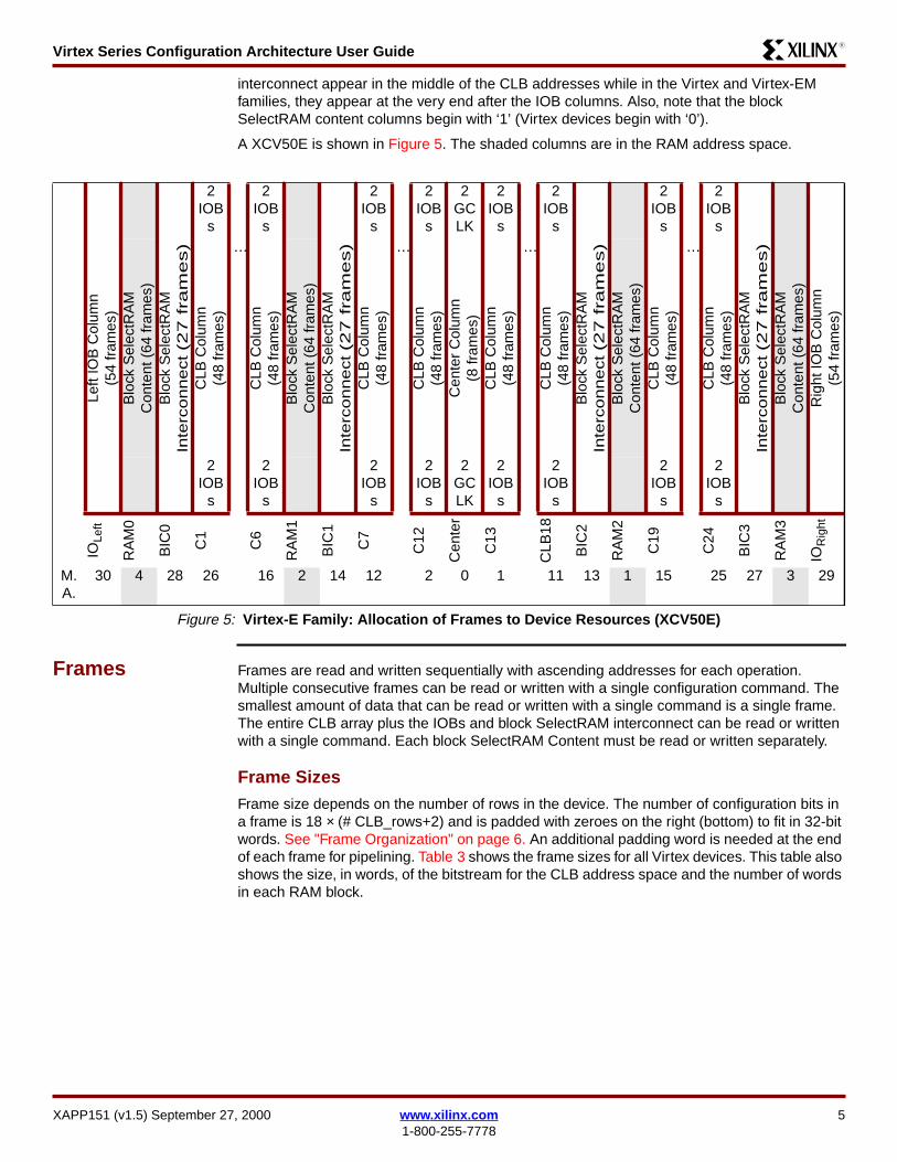
Virtex Series Configuration Architecture User GuideR13
interconnect appear in the middle of the CLB addresses while in the Virtex and Virtex-EMfamilies they appear at the very end after the IOB columns Also note that the blockSelectRAM content columns begin with lsquo1rsquo (Virtex devices begin with lsquo0rsquo)
A XCV50E is shown in Figure 5 The shaded columns are in the RAM address space
Frames Frames are read and written sequentially with ascending addresses for each operationMultiple consecutive frames can be read or written with a single configuration command Thesmallest amount of data that can be read or written with a single command is a single frameThe entire CLB array plus the IOBs and block SelectRAM interconnect can be read or writtenwith a single command Each block SelectRAM Content must be read or written separately
Frame SizesFrame size depends on the number of rows in the device The number of configuration bits ina frame is 18 times ( CLB_rows+2) and is padded with zeroes on the right (bottom) to fit in 32-bitwords See Frame Organization on page 6 An additional padding word is needed at the endof each frame for pipelining Table 3 shows the frame sizes for all Virtex devices This table alsoshows the size in words of the bitstream for the CLB address space and the number of wordsin each RAM block
2IOB
s
2IOB
s
2IOB
s
2IOB
s
2GCLK
2IOB
s
2IOB
s
Blo
ck S
elec
tRA
MIn
terc
on
ne
ct(2
7 f
ram
es)
2IOB
s
2IOB
s
Blo
ck S
elec
tRA
MC
onte
nt (
64 fr
ames
)
Left
IOB
Col
umn
(54
fram
es)
Blo
ck S
elec
tRA
MC
onte
nt (
64 fr
ames
)B
lock
Sel
ectR
AM
Inte
rco
nn
ect(2
7 f
ram
es)
CLB
Col
umn
(48
fram
es)
hellipC
LB C
olum
n(4
8 fr
ames
)B
lock
Sel
ectR
AM
Con
tent
(64
fram
es)
Blo
ck S
elec
tRA
MIn
terc
on
ne
ct(2
7 f
ram
es)
CLB
Col
umn
(48
fram
es)
hellip
CLB
Col
umn
(48
fram
es)
Cen
ter
Col
umn
(8 fr
ames
)C
LB C
olum
n(4
8 fr
ames
)
hellip
CLB
Col
umn
(48
fram
es)
Blo
ck S
elec
tRA
MC
onte
nt (
64 fr
ames
)C
LB C
olum
n(4
8 fr
ames
)
hellip
CLB
Col
umn
(48
fram
es)
Blo
ck S
elec
tRA
MIn
terc
on
ne
ct(2
7 f
ram
es)
Rig
ht IO
B C
olum
n(5
4 fr
ames
)
2IOB
s
2IOB
s
2IOB
s
2IOB
s
2GCLK
2IOB
s
2IOB
s
2IOB
s
2IOB
s
IOLe
ft
RA
M0
BIC
0
C1
C6
RA
M1
BIC
1
C7
C12
Cen
ter
C13
CLB
18
BIC
2
RA
M2
C19
C24
BIC
3
RA
M3
IOR
ight
MA
30 4 28 26 16 2 14 12 2 0 1 11 13 1 15 25 27 3 29
Figure 5 Virtex-E Family Allocation of Frames to Device Resources (XCV50E)
XAPP151 (v15) September 27 2000 wwwxilinxcom 51-800-255-7778
Virtex Series Configuration Architecture User GuideR13
Frame OrganizationEach frame sits vertically in the device with the ldquofrontrdquo of the frame at the top As shown inFigure 6 it is convenient to consider the frame horizontally when it is viewed as part of abitstream The top IOBs are shown on the left followed by the CLBs in the column and thebottom IOBs on the right Bits in frames are allocated as follows
For CLB columns the first 18 bits control the two IOBs at the top of the column then 18 bits areallocated for each CLB row finally the next 18 bits control the two IOBs at the bottom of the
Table 3 Virtex Series Devices
Device Row times ColBits
FrameWordsFrame
Virtex Virtex-E
RAMCols
of 32-bit Read-backWords (1)
RAMCols
RAMSpace
of 32-bit Read-backWords (1)
CLB(all)
RAM(1 col)
CLB(all)
RAM(1 col)
XCV50 16 times 24 384 12 2 15876 780 - - - -
XCV50E 16 times 24 384 12 - - - 4 6 16524 780
XCV100 20 times 30 448 14 2 22554 910 - - - -
XCV100E 20 times 30 448 14 - - - 4 12 23310 910
XCV150 24 times 36 512 16 2 30384 1040 - - - -
XCV200 28 times 42 576 18 2 39366 1170 - - - -
XCV200E 28 times 42 576 18 - - - 4 12 40338 1170
XCV300 32 times 48 672 21 2 51975 1365 - - - -
XCV300E 32 times 48 672 21 - - - 4 12 53109 1365
XCV400 40 times 60 800 25 2 76275 1625 - - - -
XCV400E 40 times 60 800 25 - - - 4 12 77625 1625
XCV405E 40 times 60 800 25 - - - 14 4 84375 1625
XCV600 48 times 72 960 30 2 108810 1950 - - - -
XCV600E 48 times 72 960 30 - - - 6 12 112050 1950
XCV800 56 times 84 1088 34 2 142902 2210 - - - -
XCV812E 56 times 84 1088 34 - - - 20 4 159426 2210
XCV1000 64 times 96 1248 39 2 186381 2535 - - - -
XCV1000E 64 times 96 1248 39 - - - 6 12 190593 2535
XCV1600E 72 times 108 1376 43 - - - 8 12 237231 2795
XCV2000E 80 times 120 1536 48 - - - 8 12 292464 3120
XCV2600E 92 times 138 1728 54 - - - 8 12 375678 3510
XCV3200E 104 times 156 1952 61 - - - 8 12 477081 3965
Notes1 Includes pad frame in calculation
6 wwwxilinxcom XAPP151 (v15) September 27 20001-800-255-7778
Virtex Series Configuration Architecture User GuideR13
CLB column The frame then contains enough ldquopadrdquo bits to make it an integral multiple of 32bits
For IOB columns the frame allocates 18 bits per three IOB rows Figure 7 When reading andwriting frames bits are grouped into 32-bit words starting on the left (corresponding to the topof the device) If the last word does not completely fill a 32-bit word it is padded on the right withzeroes
For block SelectRAM content columns (Figure 8) the first 18 bits are pad bits then 72 bits areallocated for each RAM row finally there are another 18 pad bits The frame then adds enoughldquopadrdquo bits to make it an integral multiple of 32 bits
Location of LUT SelectRAM BitsWith respect to the beginning of a configuration frame relative locations of LUT SelectRAM bitswithin the bitstream are the same for every CLB slice The bits of a LUT SelectRAM are spreadacross 16 consecutive frame Minor Addresses Each frame Minor Address contains allinstances of a single bit index for that column These 16 frames contain all 16 bits of the LUTSelectRAM for a column of CLB slices You must read or write the 16 frames containing thosebits to read or write the entire LUT SelectRAM
Figure 6 CLB Column Frame Organization
Figure 7 IOB Column Frame Organization
Figure 8 Block SelectRAM Content Column Frame Organization
Note LUT SelectRAM bits are stored inverted Flip-Flop data are stored in their true senseWhen reading or writing LUT SelectRAM data from the bitstream it is negated from the logicsense of the data For example a 4-input AND gate has the truth tableLUT[150] = 1000000000000000
This truth table isstored internally in theLUTSelectRAMasLUT[150] = 0111111111111111Ofcourse user logic reading the data from the LUT SelectRAM would read the correct logicvalue LUT[150] = 1000000000000000
Top 2 IOBs13 Bottom 2 IOBs1313
CLB Rn1313
13 18131813181318131813
CLB R213CLB R113
x151_06_020700
Top 3 IOBs Bottom 3 IOBs1313
181818
3 IOBs
x151_07_020800
Pad PadRAM Rn
1872727218
RAM R1RAM R0
x151_08_021800
XAPP151 (v15) September 27 2000 wwwxilinxcom 71-800-255-7778
Virtex Series Configuration Architecture User GuideR13
ConfigurationData Operations
Reading Configuration DataConfiguration information can be read from the Virtex devices if readback is enabled in thecurrent configuration (See the description of the Control Register field SBITS on page 21)CLB and IOB configuration data can be read while the device is operating
When reading data from a Virtex device a pad frame is read before any of the data framesThis is in addition to the pad word in each data frame The pad frame must be included in theword count to be read from the device
Each frame read from the device consists of the number of words shown in Table 3
For example the XCV150 has 16-word frames When reading frames the first word of a frameis a pad word Including the pad frame the XCV150 has 1899 (3038416) frames (SeeFigure 9)
Writing Configuration DataConfiguration information can be written to a Virtex device while the device is running if writingis enabled in the current configuration (See the Control Register field SBITS in Table 23) Re-writing the same configuration data does not generate any transient signals
Changing configuration data may generate transient signals especially if LUT values or signalrouting is changed For this case all the logic cells and routing can be placed in a non-contentious state by asserting the GHIGH_B signal See the description for the CommandRegister (CMD) on page 18
When writing configuration data to the Virtex device whether from the SelectMAP or JTAGinterfaces the data frames are written to the device with each frame followed by a pad wordAfter all the data frames are written a pad frame must be written (to flush internal pipelines)The pad words and pad frame must be included in the number of words to be written to thedevice (Table 3)
For example the XCV1000 has 39-word frames When writing frames the last word of theframe is a pad word Including the pad frame the XCV1000 has 4779 (18638139) framesSee Figure 10)
Altering Configuration DataVirtex devices support the Read-Modify-Write (RMW) method of changing LUT SelectRAMdata Therefore it is possible to read or alter the contents of one or more LUT SelectRAMsthrough the JTAG or SelectMAP interfaces When writing data to one or more LUTSelectRAMs all the bits in the frame must have valid configuration information This can beassured by altering valid configurations from bitstream files or from frames read from a properlyconfigured Virtex device When using the RMW method it may be expeditious to read the dataignoring the pad frame and the pad word of only the first frame This aligns the remaining
Pad Frame (16 words)Pad Word Data Frame 0 (15 words)
hellip
hellip
Pad Word Data Frame n (15 words)
Figure 9 XCV150 Frame Padding for Device Read
Data Frame 0 (38 words) Pad Word
hellip
Data Frame n (38 words) Pad WordPad Frame (39 words)
Figure 10 XCV1000 Frame Padding for Device Write
8 wwwxilinxcom XAPP151 (v15) September 27 20001-800-255-7778
Virtex Series Configuration Architecture User GuideR13
configuration data in the Device Write format After modifying the configuration the altered datacan be written to the Virtex device followed by a pad word and a pad frame
It is not necessary to retain the contents of the pad frame or pad words However pad wordsand pad frames are included in the CRC calculation
Definitions Two sets of variables are defined to determine where a desired bit is in the configuration dataThe first is a set of ldquoindependentrdquo variables or design attributes namely characteristics of thedesign that are known ie the device size and which CLB and bit(s) within the CLB to locateTable 4 The second set is a set of ldquodependentrdquo variables or design variables namely valuesthat must be calculated to find the bit(s) of interest listed in Table 5
Note Frames span an entire column of CLB slices (or IOBs) Thus when changing LUTSelectRAM bit 0 for a single CLB slice (eg R3C4S1) LUT SelectRAM bit 0 for all slices inthat column (ie RC4S1) is written with the same command One must ensure that either allother data in the slice is constant or changed externally through partial configurations
LUT SelectRAMs not configured externally should not lie in the same slice with LUTs or LUTSelectRAMs that are re-configured externally Such a mixture can cause the unrelated LUTSelectRAM data to be re-configured when the frames are written to the device Figure 11shows what can happen if this restriction is not observed
In this example it is the objective to perform a Read-Modify-Write on the LUT SelectRAM inR2C3S1 in column 3 which is shown in the first column in the figure Row 2 contains a LUTcontaining the value AB Row 3 contains a SelectRAM containing the value C3 Because theRead and Write operations operate on an entire frame the RAM in R3C3S1 is also read andwritten when R2C3S1 is read and written Performing the Readback operation reads all theLUT and SelectRAM values for the column Before the new value for the LUT is written it ispossible for the on-chip circuitry to write a new value such as 14 into the SelectRAM Whenthe new value BD is written via the configuration interface into LUT R2C3S1 the value C3 isalso written into RAM R3C3S1 This may not always be desirable (It is design-dependent)
Figure 11 Potential Write Conflicts
x151_11_020800
LUT R2C3S113AB13
RAM R3C3S113C313
Before13Readback
13
LUT R2C3S113AB13
RAM R3C3S1131413
Before13Configuration 13
Write
13
LUT R2C3S113BD13
RAM R3C3S113C313
After13Configuration13
Write
13
Table 4 Design Attributes (Independent Variables)
Term Definition
Chip_Cols of CLB columns on the Virtex device
Chip_Rows of CLB rows on the Virtex device
Chip_Rams of block SelectRAM columns on the Virtex device
RAM_Space Spacing of block SelectRAM columns (in terms of CLB columns)
FL of 32-bit words in the frame
XAPP151 (v15) September 27 2000 wwwxilinxcom 91-800-255-7778
Virtex Series Configuration Architecture User GuideR13
RW 1 for Read 0 for Write
CLB_Col Column number of the desired CLB
CLB_Row Row number of the desired CLB
Slice 0 or 1
FG 0 for the F-LUT 1 for the G-LUT
lut_bit The desired bit from the given LUT Bits in the LUT are indexed from 0 to 15
XY 0 for the X Flip-Flop 1 for the Y Flip-Flop
RAM_Col Column number of the desired block SelectRAM
RAM_Row Row number of the desired block SelectRAM
ram_bit The desired bit from the given block SelectRAM Bits are indexed from 0 to4095
Table 5 Design Variables (Dependent Variables)
Term Definition
MJA Frame Major Address
MNA Frame Minor Address
fm_st_wd The index of the word within a full configuration segment that correspondsto the starting word of the desired frame A full configuration segment isdefined as the following 1) for CLBIOB all CLB IOB and RAMinterconnect frames beginning at MJA=0 MNA=0 and 2) for blockSelectRAM all RAM content frames for the given RAM column Words arenumbered starting at 0
fm_wd The index of the 32-bit word within a frame that contains the desired bitWords in a frame are numbered starting at 0
fm_wd_bit_idx The bit index of the desired bit within frame word fm_wd Words areindexed in ldquobig-endianrdquo style with bit 31 on the left and bit 0 on the right
fm_bit_idx Bit index within a frame of the desired bit Numbered starting with 0 as theleft-most (first) bit Bit numbering within a frame continues across all thewords in the frame
Table 6 Functions used in Equations
Functions Definition
floor(x) The largest integer not larger than x Eg floor(31) = 3 because the nextlargest integer 4 is larger than 31 floor(3)=3
ceiling(x) The smallest integer greater than or equal to x For example ceiling(32) = 4because 4 is greater than 32 and 3 is not ceiling (4) = 4
The modulus operation 5 2 = 1 5 3 = 2 5 5 = 0
Table 4 Design Attributes (Independent Variables) (Continued)
Term Definition
10 wwwxilinxcom XAPP151 (v15) September 27 20001-800-255-7778
Virtex Series Configuration Architecture User GuideR13
CLB LUTSelectRAMDependentVariables
Table 7 shows equations for the LUT SelectRAM ldquoDependent Variablesrdquo that were defined inTable 5
Virtex-E CLB LUT SelectRAM Dependent VariablesThe additional block SelectRAM columns in Virtex-E devices require an adjustment to the MJAThe following equations calculate the adjustment necessary for each of the affected dependentvariables For each variable calculate the base value based upon the Virtex equations onlyand then add the resulting Virtex adjustment
The left and right sides of the device are treated differently
LUT SelectRAM ExamplesSee ldquoExamplesrdquo on page 27 for several examples of reading and evaluating configuration dataThe examples illustrate how to make use of these equations to find the desired data in abitstream
Table 7 Virtex Equations for LUT SelectRAM Dependent Variables
Term Definition
MJA if (CLB_Col le Chip_Cols2)then Chip_Cols ndash CLB_Col times 2 + 2else 2 times CLB_Col ndash Chip_Cols ndash 1
MNA lut_bit + 32 ndash Slice times (2 times lut_bit + 17)
fm_bit_idx 3 + 18 times CLB_Row ndash FG + RW times 32
fm_st_wd FL times (8 + (MJA ndash1) times 48 + MNA) + RW times FL
fm_wd floor(fm_bit_idx32)
fm_wd_bit_idx 31 + 32 times fm_wd ndash fm_bit_idx
Notes
bull Do NOT input the final results back into the original Virtex equations (eg do not useMJAfinal value to calculate fm_st_wd)
bull MJAfinal = MJA + MJA_adj
bull fm_st_wdfinal = fm_st_wd + fm_st_wd_adj
Table 8 CLB Location
CLB Location CLB Column
Left CLB_Col le Chip_Cols2
Right CLB_Col gt Chip_Cols2
Table 9 Virtex-E Families Adjustments for LUT SelectRAM Dependent Variables
Term Definition
MJA_adj Left RAM_Bound = (Chip_Rams2 - 1) x RAM_SpaceMJA_adj = 2 x ceiling((RAM_Bound - CLB_Col + 1) RAM_Space)
Right
RAM_Bound = Chip_Cols - (Chip_Rams2 - 1) x RAM_Space + 1MJA_adj = 2 x ceiling((CLB_Col - RAM_Bound + 1) RAM_Space)
fm_st_wd_adj FL times (27 x MJA_adj)
XAPP151 (v15) September 27 2000 wwwxilinxcom 111-800-255-7778
Virtex Series Configuration Architecture User GuideR13
CLB Flip-FlopDependentVariables
Equations for the CLB flip-flops can be found in Table 10 Their locations are calculatedsimilarly to the LUT SelectRAM locations Equations for the CLB FF Dependent Variables aredefined in Table 5
Virtex-E CLB Flip-Flop Dependent VariablesApply the adjustments given in Table 8 and Table 9
IOB DependentVariables
Each IOB contains four values that can be captured into special registers These values are
bull I mdash the input flip-flop
bull O mdash the output flip-flop
bull T mdash the flip-flop for the tri-state control
bull P mdash the value of the IO pad
These values are captured by utilizing the CAPTURE_VIRTEX symbol in your design TheLibraries Guide has more details on the use of this symbol The following registers will be readas part of the readback data
Access to the IOB flip-flops is different for the top and bottom IOBs versus the left and rightIOBs
The top and bottom IOBs are part of the CLB column frames There are two IOBs at the top andbottom of each CLB column
The left and right IOBs are in columns by themselves There are three IOBs per CLB row
IOBs are numbered clockwise around the die Pad 1 is located at the left side of the top edgeabove CLB column 1 The equations for where to find IOB flip-flops in the bitstream are basedon the pad number which is the same for a given size device not the package pin name whichvaries from package to package The mapping from package pin names to pad numbers canbe found in EPIC or fpga_editor
Table 11 contains the numeric pad indices for the pads on all four edges of the device in termsof the number of CLB columns and rows on the device
Table 10 Virtex Equations for CLB FF Dependent Variables
Term Definition
MJA if (CLB_Col le Chip_Cols2)then Chip_Cols ndash CLB_Col times 2 + 2else 2 times CLB_Col ndash Chip_Cols ndash 1
MNA Slice times (12 times XY ndash 43) ndash 6 times XY + 45
fm_bit_idx (18 times CLB_Row) + 1 + (32 times RW)
fm_st_wd FL times (8 + (MJA ndash1) times 48 + MNA) + RW times FL
fm_wd floor(fm_bit_idx32)
fm_wd_bit_idx 31 + 32 times fm_wd ndash fm_bit_idx
12 wwwxilinxcom XAPP151 (v15) September 27 20001-800-255-7778
Virtex Series Configuration Architecture User GuideR13
Table 12 shows the equations for the dependent variables for the IOB flip-flops The variable iin this table refers to the index of pad i
Table 11 IOB Pad Indices
PadLocation Pad Index i
Top 1 le i le Chip_Cols times 2
Right Chip_Cols times 2 +1 le i le Chip_Cols times 2 + Chip_Rows times 3
Bottom Chip_Cols times 2 + Chip_Rows times 3 + 1 le i le Chip_Cols times 4 + Chip_Rows times 3
Left Chip_Cols times 4 + Chip_Rows times 3 + 1 le i le Chip_Cols times 4 + Chip_Rows times 6
Table 12 Equations for IOB Dependent Variables
Term Definition
MJA
Topif (i le Chip_Cols)then Chip_Cols ndash ceiling(i2) times 2 + 2else 2 times ceiling (i2) ndash Chip_Cols ndash1
Right Chip_Cols + 1
Bottomif (i gt 3 times (Chip_Cols + Chip_Rows))then 2 times ceiling((i ndash 3 times Chip_Cols ndash 3 times Chip_Rows)2)else Chip_Cols ndash 2 times floor((i ndash 2 times Chip_Cols ndash 3 times Chip_Rows ndash 1)2) ndash 1
Left Chip_Cols + 2
MNA
Top
I ndash 25 times (i2) + 45
O ndash 13 times (i2) + 39
T ndash 5 times (i2) + 35
P ndash 4 times (i2) + 25
Right
I t = (i ndash 2 times Chip_Cols) 3 MNA = 275 times t2 ndash 575 times t + 32
O t = (i ndash 2 times Chip_Cols) 3 MNA = 215 times t2 ndash 515 times t + 38
T t = (i ndash 2 times Chip_Cols) 3 MNA = 175 times t2 ndash 475 times t + 42
P 50
Bottom
I 25 times ((i ndash 2 x Chip_Cols - 3 x Chip_Rows)2) + 20
O 13 times ((i ndash 2 x Chip_Cols - 3 x Chip_Rows)2) + 26
T 5 times ((i ndash 2 x Chip_Cols - 3 x Chip_Rows)2) + 30
P 4 times ((i ndash 2 x Chip_Cols - 3 x Chip_Rows)2) + 21
Left
I t = (i ndash 4 x Chip_Cols - 3 x Chip_Rows)3 MNA = 175 times t2 ndash 475 times t + 45
O t = (i ndash 4 x Chip_Cols - 3 x Chip_Rows)3 MNA = 235 times t2 ndash 535 times t + 39
T t = (i ndash 4 x Chip_Cols - 3 x Chip_Rows)3 MNA = 275 times t2 ndash 575 times t + 35
P 50
XAPP151 (v15) September 27 2000 wwwxilinxcom 131-800-255-7778
Virtex Series Configuration Architecture User GuideR13
Virtex-E IOB Dependent VariablesSimilar to CLB dependent variables only the variables affected by the major address aredifferent in Virtex-E and Virtex-EM devices versus Virtex devices A simple way to account forthe change is to determine the CLB column where the pad resides (only true for top andbottom) Then the adjustment calculated for the CLB column can be applied The conversionto CLB columns is found in Table 13
fm_bit_idx
Top 32 times RW
Right
I O ampT 18 times (1 + floor ((i ndash 2 times Chip_Cols ndash 1)3)) + 32 times RW
Pt = (i ndash 2 times Chip_Cols) 3fm_bit_idx = 18 times (1 + floor ((i ndash 2 times Chip_Cols ndash 1)3)) + 6 times t2 ndash 17 times t + 15 + 32 timesRW
Bottom 18 times (Chip_Rows + 1)+ 32 times RW
Left
I O ampT18 times (Chip_Rows ndash floor((i ndash 4 times Chip_Cols ndash 3 times Chip_Rows ndash 1)3)) + 32 times RW
Pt = (i ndash 4 times Chip_Cols ndash 3 times Chip_Rows)3fm_bit_idx = 18 times (Chip_Rows ndash floor ((i ndash 4 times Chip_Cols ndash 3 times Chip_Rows ndash 1)3))ndash 105 times t2 + 215 times t + 4 + 32 times RW
fm_st_wdif (MJA gt Chip_Cols + 1)then FL times (54 times MJA ndash 46 + MNA ndash 6 times Chip_Cols) + RW times FLelse FL times (8 + (MJA ndash1) times 48 + MNA) + RW times FL
fm_wd floor (fm_bit_idx32)
fm_wd_bit_idx 31 + 32 times fm_wd ndash fm_bit_idx
Table 12 Equations for IOB Dependent Variables (Continued)
Term Definition
Table 13 Pad -gt CLB Column
Term Definition
CLB_ColTop ceiling(i2)
Bottom ceiling((4 x Chip_Cols + 3 x Chip_Rows + 1 - i)2)
Table 14 Virtex-E Families Adjustments for IOB Dependent Variables
Term Definition
MJA_adj
Top use Table 8 and Table 9
Right Chip_Rams
Bottom use Table 8 and Table 9
Left Chip_Rams
fm_st_wd_adj FL times (27 x MJA_adj)
14 wwwxilinxcom XAPP151 (v15) September 27 20001-800-255-7778
Virtex Series Configuration Architecture User GuideR13
BlockSelectRAMDependentVariables
The equations for the block SelectRAM dependent variables are given in Table 15 Therelationship of a particular memory cell index in the context of a given configuration is describedin XAPP130 ldquoUsing the Vir tex Bloc k SelectRAM+ Resour cerdquo
Virtex-E Block SelectRAM Dependent VariablesThe RAM major address numbering scheme changed slightly such that the lowest MJA on theleft side is now 2 instead of 0 As in the case for the CLB equations the adjustments belowshould be applied after the Virtex equations
Table 15 Virtex Equations for Block SelectRAM Dependent Variables
Term Definition
MJAif (RAM_Col lt Chip_Rams2)then 2 x (Chip_Rams2 - 1 - RAM_Col)else 2 x (RAM_Col - Chip_Rams2) + 1
MNA
1 x floor(((ram_bit 64) 64)32) + 2 x floor(((ram_bit 64) 32)16)+ 4 x floor(((ram_bit 64) 16)8) + 8 x floor(((ram_bit 64) 8)4)+ 16 x floor(((ram_bit 64) 4)2) + 32 x floor(((ram_bit 64) 2)1)equivalent to MNA = div64[05] where div64[50] = floor(ram_bit64)
fm_bit_idxobtain value for bitpos from Table 16
fm_bit_idx = 18 + 72 x RAM_Row + bitpos
fm_st_wd FL times MNA + RW times FL
fm_wd floor(fm_bit_idx32)
fm_wd_bit_idx 31 + 32 times fm_wd ndash fm_bit_idx
Table 16 Virtex Block SelectRAM Bit Position Within a Given Block SelectRAM
ram
_bit
6
4
bitp
os
ram
_bit
6
4
bitp
os
ram
_bit
6
4
bitp
os
ram
_bit
6
4
bitp
os
ram
_bit
6
4
bitp
os
ram
_bit
6
4
bitp
os
ram
_bit
6
4
bitp
os
ram
_bit
6
4
bitp
os
0 42 8 45 16 29 24 26 32 43 40 44 48 28 56 27
1 58 9 61 17 13 25 10 33 59 41 60 49 12 57 11
2 41 10 46 18 30 26 25 34 40 42 47 50 31 58 24
3 57 11 62 19 14 27 9 35 56 43 63 51 15 59 8
4 50 12 53 20 21 28 18 36 51 44 52 52 20 60 19
5 49 13 54 21 22 29 17 37 48 45 55 53 23 61 16
6 66 14 69 22 5 30 2 38 67 46 68 54 4 62 3
7 65 15 70 23 6 31 1 39 64 47 71 55 7 63 0
Table 17 Virtex-E and Virtex-EM Adjustments for Block SelectRAM DependentVariables
Term Definition
MJA_adj if (RAM_Col lt Chip_Rams2) MJA_adj = 2
XAPP151 (v15) September 27 2000 wwwxilinxcom 151-800-255-7778
Virtex Series Configuration Architecture User GuideR13
ConfigurationLogic Basics
Configuration DataConfiguration data is organized as 32-bit words There are two major commands that theconfiguration data can contain Read and Write A configuration command is executed whenthe configuration command is read or written to the appropriate command register
The OP field contains 01 for a Read operation and 10 for a Write operation (See Figure 12)
A command is organized as a packet with a header word and optional data words The headerword is the first word written to the appropriate command register for a read or write operationThe header word contains a type field (001) an operand field a register address field and aword count field The format for the command header is shown in Figure 13 on page 17
The Register Address field defines the target of this command as defined in Table 18 on page17
The header word count field contains an integer between 0 and 2047 and indicates thenumber of words that follow the header Larger word counts (between 2048 and 1048575words) are achieved by setting the header word count to 0 The Extension header word has atype field = 010 an OP field that must match the OP field in the preceding Command Headerword and a 20-bit word count this format is shown Figure 14 on page 17
Configuration FlowVirtex devices are configured by presenting configuration data to the SelectMAP or JTAGinterfaces in a specific sequence
For Initial Configuration
1 Issue one or more pad words (SelectMAP only)
2 Issue Sync word (SelectMAP only)
3 Reset CRC
4 Set FLR
5 Set COR
6 Set MASK
7 Set CTL (Set PERSIST if you want to keep SelectMAP active after this configuration)
8 Issue a SWITCH (switch CCLK frequency) command to the CMD register This isnecessary only in Master Serial configuration mode
Reading Configuration
These commands can be issued to read a full configuration or for a partial configuration afterthe device has been completely configured
1 Issue a Sync word (SelectMAP only) if the previous configuration command was aborted
2 Set the FAR to the starting address
3 Issue a RCFG (read configuration) command to the CMD register
4 Write the number of words to be read to the FDRO register
5 Flush the command pipeline with a pad word
6 Read data frames
OP CODERead 01Write 10
Figure 12 OP Field Code
16 wwwxilinxcom XAPP151 (v15) September 27 20001-800-255-7778
Virtex Series Configuration Architecture User GuideR13
Writing Configuration
These commands can be issued either as part of an initial configuration or for a partialconfiguration after the device has been configured
1 Issue a Sync word (SelectMAP only) if the previous configuration command was aborted
2 If the frames being written can cause contention then assert the GHIGH_B signal
3 Set the FAR to the starting address
4 Issue a WCFG (write configuration) command to the CMD register
5 Write the number of words to be written to the FDRI register
6 Write data frames
7 If the GHIGH_B signal was asserted de-assert it by writing the LFRM (Last Frame)command to the CMD register and write one pad frame
ConfigurationRegisters
Configuration logic is accessed and controlled via a collection of 32-bit registers called theconfiguration registers (see Table 18) Registers are described in the following sections
Type OP Register Address RSV Word Count31 30 29 28 27 26 25 24 23 22 21 20 19 18 17 16 15 14 13 12 11 10 9 8 7 6 5 4 3 2 1 00 0 1 x x 0 0 0 0 0 0 0 0 0 0 x x x x 0 0 x x x x x x x x x x x
Notes1 Locations within fields containing a zero or one must have these values An X in a bit field indicates that the value is variable and must
be set2 Heavy vertical lines are used to separate fields Light vertical lines separate nibbles in the word
Figure 13 Command Header Format
Type OP Word Count31 30 29 28 27 26 25 24 23 22 21 20 19 18 17 16 15 14 13 12 11 10 9 8 7 6 5 4 3 2 1 00 1 0 x x 0 0 0 0 0 0 0 x x x x x x x x x x x x x x x x x x x x
Notes1 Locations within fields containing a zero or one must have these values An X in a bit field indicates that the value is variable and must
be set2 Heavy vertical lines are used to separate fields Light vertical lines separate nibbles in the word
Figure 14 Large Block Count Header Extension Format
Table 18 Configuration Register Addresses
Register Name Mnemonic RW Binary Address
CRC CRC RW 0000
Frame Address FAR RW 0001
Frame Data Input FDRI W 0010
Frame Data Output FDRO R 0011
Command CMD RW 0100
Control CTL RW 0101
Control Mask MASK RW 0110
Status STAT R 0111
Legacy Output LOUT W 1000
XAPP151 (v15) September 27 2000 wwwxilinxcom 171-800-255-7778
Virtex Series Configuration Architecture User GuideR13
Command Register (CMD)The content of the Command Register (CMD) is interpreted by the configuration state machineConfiguration commands control the operation of the configuration state machine the FrameData Register (FDR) and some of the global signals The command in the Command Registeris executed each time the FAR is loaded with a new value The effect of each command isdefined in Table 19
Configuration Option COR RW 1001
Reserved mdash mdash 1010
Frame Length FLR RW 1011
Reserved mdash mdash 1100
Reserved mdash mdash 1101
Reserved mdash mdash 1110
Reserved mdash mdash 1111
Table 18 Configuration Register Addresses (Continued)
Register Name Mnemonic RW Binary Address
Table 19 Configuration Commands
Cmd Code Description
Rsvd 0000 Reserved
WCFG 0001Write Configuration Data mdash Used prior to writing configuration data to the FDRI It takes theinternal configuration state machine through a sequence of states that control the shifting of the FDRand the writing of the configuration memory (See Frame Data Input Register (FDRI) on page 24)
Rsvd 0010 Reserved
LFRM 0011Last Frame mdash This command is loaded prior to writing the last (pad) data frame if the GHIGH_Bsignal was asserted This command is not necessary if the GHIGH_B signal was not asserted Thisallows overlap of the last frame write with the release of the GHIGH_B signal
RCFG 0100Read Configuration Data mdash Used prior to reading frame data from the FDRO Similar to the WCFGcommand in its effect on the FDR (see Frame Data Output Register (FDRO) on page 24)
START 0101Begin Startup Sequence mdash Starts the startup sequence This command is also used to start ashutdown sequence prior to partial re-configuration The Startup Sequence begins with the nextsuccessful CRC check (see Cyclic Redundancy Check (CRC) on page 22)
RCAP 0110Reset Capture mdash Used when performing capture in single-shot mode This command must be usedto reset the capture signal if single-shot capture has been selected
RCRC 0111 Reset CRC mdash Used to reset CRC register (see Cyclic Redundancy Check (CRC) on page 22)
AGHIGH 1000Assert GHIGH_B Signal mdash Used prior to re-configuration to prevent contention while writing newconfiguration data All CLB outputs and signals are forced to a one
SWITCH 1001Switch CCLK Frequency mdash Used to change (increase) the frequency of the Master CCLK Thenew frequency is specified in Table 21
Rsvd 1010 Reserved
Rsvd 1011 Reserved
Rsvd 1100 Reserved
18 wwwxilinxcom XAPP151 (v15) September 27 20001-800-255-7778
Virtex Series Configuration Architecture User GuideR13
Configuration Option Register (COR)The Configuration Option Register (COR) is used to select configuration options that areillustrated in Figure 15 and defined in Table 20 Entries in this table are further explained in thefollowing tables
Rsvd 1101 Reserved
Rsvd 1110 Reserved
Rsvd 1111 Reserved
Table 19 Configuration Commands (Continued)
Cmd Code Description
DO
NE
_PIP
E
DR
IVE
_DO
NE
SIN
GLE
OS
CF
SE
L
SS
CLK
SR
C
LOC
K_W
AIT
SH
UT
DO
WN
DO
NE
_CY
CLE
LCK
_CY
CLE
GT
S_C
YC
LE
GW
E_C
YC
LE
GS
R_C
YC
LE
31 30 29 28 27 26 25 24 23 22 21 20 19 18 17 16 15 14 13 12 11 10 9 8 7 6 5 4 3 2 1 00 x x x x x x x x x x x x x x x x x x x x x x x x x x x x x x x
Notes1 Locations within fields containing a zero or one must have these values An X in a bit field indicates that the value is variable and must
be set2 Heavy vertical lines are used to separate fields Light vertical lines separate nibbles in the word
Figure 15 COR (Configuration of Option Register) Fields
XAPP151 (v15) September 27 2000 wwwxilinxcom 191-800-255-7778
Virtex Series Configuration Architecture User GuideR13
Table 21 shows the allowed values for the OSCFSEL field of the COR Setting OSCFSEL toone of these values will set the Master CCLK frequency to the specified value
Table 20 Configuration Option Register Fields
Field Bit Indices DescriptionBitgenDefault
DONE_PIPE 30
0 No pipeline stage for DONEIN
1 Add pipeline stage to DONEINFPGA waits on DONE that is delayed by one (1) cycle of the StartupClkrather than the pin itself Use this option when StartupClk is running at highspeeds
0
DRIVE_DONE 290 DONE pin is open drain
1 DONE pin is actively driven high0
SINGLE 28 Readback capture is one-shot 0
OSCFSEL 2722 Select CCLK frequency in Master Serial configuration mode 2
SSCLKSRC 2120
Startup sequence clock source00 Cclk01 UserClk1x JTAGClk
0
LOCK_WAIT 1916
4-bit mask indicating which DLL lock signals to wait for during LCK cycleThe 4 bits (from MSB to LSB) correspond to DLLs TL=3 TR=2 BL=1BR=0 (top-left top-right etc) In Virtex-E devices where there are 8 DLLseach mask bit applies to the 2 DLLs in that quadrant of the device Thedefault is not to wait for any DLL lock signals
0
SHUTDOWN 15
Indicate whether doing a startup or shutdown sequence
0 Startup
1 Shutdown sequence
0
DONE_CYCLE 1412 Startup phase in which DONE pin is released 3
LCK_CYCLE 119 Stall in this startup phase until DLL locks are asserted 7
GTS_CYCLE 86 Startup phase in which IOs switch from tri-state to user design 4
GWE_CYCLE 53 Startup phase in which the global write-enable is asserted 5
GSR_CYCLE 20 Startup phase in which the global setreset is negated 5
Table 21 OSCFSEL-Specified Master CCLK Frequencies)
CCLK(MHz) OSCFSEL
CCLK(MHz) OSCFSEL
CCLK(MHz) OSCFSEL
43 000010 13 001010 41 100111
54 010001 15 001101 45 110011
69 000100 20 010111 51 101010
81 000101 26 011010 55 110100
20 wwwxilinxcom XAPP151 (v15) September 27 20001-800-255-7778
Virtex Series Configuration Architecture User GuideR13
Table 22 shows the values of the DONE_CYCLE LCK_CYCLE GTS_CYCLE GWE_CYCLEand GSR_CYCLE fields in COR This table shows the step in the start-up sequence when eachof these signals becomes active
Control Register (CTL)The Control Register (CTL) fields are illustrated in Figure 16 on page 21 and defined inTable 23
92 000110 30 011101 60 101101
100 000111 34 110010 mdash mdash
Notes1 These values are accurate to +45 ndash 30
Table 22 COR Startup Cycle Fields
FieldValue
DONE_CYCLE(DONE Active)
GTS_CYCLE(GTS_CFGInactive)
GSR_CYCLE(GSR Inactive)
GWE_CYCLE(GWE Active) LCK_CYCLE
000 1 1 1 1 0
001 2 2 2 2 1
010 3 3 3 3 2
011 4 (default) 4 4 4 3
100 5 5 (default) 5 5 4
101 6 6 6 (default) 6 (default) 5
110 mdash DoneIndagger DoneIndagger DoneIndagger 6
111 Keep State Keep State Keep State Keep State Donrsquot Wait(default)
Notes1 dagger DONE if DonePipe = No else the delayed version of DONE
Table 21 OSCFSEL-Specified Master CCLK Frequencies) (Continued)
CCLK(MHz) OSCFSEL
CCLK(MHz) OSCFSEL
CCLK(MHz) OSCFSEL
SB
ITS
PE
RS
IST
GT
S_U
SR
_B
31 30 29 28 27 26 25 24 23 22 21 20 19 18 17 16 15 14 13 12 11 10 9 8 7 6 5 4 3 2 1 00 0 0 0 0 0 0 0 0 0 0 0 0 0 0 0 0 0 0 0 0 0 0 x x x 0 0 0 0 0 x
Notes1 Locations within fields containing a zero or one must have these values An X in a bit field indicates that the value is variable and must
be set2 Heavy vertical lines are used to separate fields Light vertical lines separate nibbles in the word
Figure 16 Control Register Fields
XAPP151 (v15) September 27 2000 wwwxilinxcom 211-800-255-7778
Virtex Series Configuration Architecture User GuideR13
Cyclic Redundancy Check (CRC)A data input error checking mechanism is provided through the Cyclic Redundancy Check(CRC) register When data is written to any configuration register (except LOUT) a 16-bit CRCvalue is calculated using both the register data and the address This value is saved in the CRCregister At the end of any series of writes a pre-calculated CRC block-check value may bewritten to the CRC register If the resulting value is non-zero an error is indicated TheCRC_ERROR bit is accessible through the status register If a CRC error is detectedconfiguration logic is put in the ERROR mode The following section is an algorithm forcomputing CRC
CRC Algorithm Initialization bcc = 0skip_pad = truemore_words = true Check for write operation do
w = next_wordif (w[3127] == rsquo00101rsquo)
A Read OP Donrsquot use in CRCwc = w[100]if (wc == 0)
w = next_wordwc = w[190]
while (wc-- gt 0)
w = next_word
elsif (w[3127] == rsquo00110rsquo)
A Write OP Use in CRC addr = w[1613]if (addr Π0124569DB)
wc = w[100]if (wc == 0)
wc is in next word w = next_wordwc = w[190]
while (wc-- gt 0)
w = next_wordsw[350] = addr wordfor (i=0 ilt36 i++)
Table 23 Control Register Bits
NameBit
Indices Description
SBITS 87 Security level0 ReadWrite OK (default)1 Readback disabled23 Readback disabled Writing disabled except CRCregister
PERSIST 6 Configuration interface remains after configuration0 No (default)1 Yes
GTS_USR_B 0 Active-low global tristate IOs Turn off pull-ups ifGTS_CFG_B is also asserted
22 wwwxilinxcom XAPP151 (v15) September 27 20001-800-255-7778
Virtex Series Configuration Architecture User GuideR13
x16 = bcc[15] XOR sw[i]x15 = bcc[14] XOR x16x2 = bcc[1] XOR x16bcc[150] =
x15bcc[132]x2bcc[0]x16 Note the bit order crc[150] = bcc[015]
else
Pad word - ignore
while (more_words)
Frame Address Register (FAR)The Frame Address Register (FAR) holds the address of the current frame The address isdivided into three parts the block type the major address and the minor address The blocktype field indicates whether the CLB or block RAM address space is used The command in thecommand register is executed each time the FAR is loaded with a new value
The major address selects the CLB or RAM column the minor address selects the frame withinthe column The minor address is incremented each time a full data frame is read from orwritten to the frame data register If the last frame within the CLB column is selected when theincrement occurs the major address is incremented and the minor address is reset to zerootherwise the minor address is incremented However the block RAM major address is notincremented automatically
See Figure 18 for the definitions of valid values for the block type field The FAR field definitionsare shown in Figure 19
Figure 17 CRC Calculation Register
Note the Block RAM Major Address is not incremented automatically To address a differentBlock RAM Content column the FAR must be loaded with the new Major Address
Type CodesCLB 00RAM 01
Figure 18 Block Type Codes
x151_17_021100
15141312111098765432
1013
01234526272829303101
Address 32-bit Data Word
CRC Calculation Register
CRC Data Input Register
CRC Register [310]
DATA_IN
SHIFT
23
16-bit CRC13150
0000 0000 0000 0000133116
1313
XAPP151 (v15) September 27 2000 wwwxilinxcom 231-800-255-7778
Virtex Series Configuration Architecture User GuideR13
Frame Data Input Register (FDRI)The Frame Data Input Register (FDRI) is used to load configuration frame data into a Virtexdevice
The Frame Data Register (FDR) is a shift register into which data is loaded prior to transfer tothe configuration memory Configuration data is written to the Virtex device by loading thecommand register with the WCFG command and then loading the FDR with at least two framesof 32-bit words
The write operation is pipelined such that the first frame of data is written to the configurationmemory while the second frame is being shifted in The last frame (the pad frame) is alwaysdummy data which is not actually written to the configuration memory Each frame write mustinclude enough 32 bit data words to load the frame fully There is one pad word at the end ofeach frame which is required for the pipelining hardware
Frame Data Output Register (FDRO)The Frame Data Output Register (FDRO) is for reading configuration data or captured datafrom the Virtex device a process called readback Readback is performed by loading thecommand register with the RCFG command and then addressing the FDRO with a readcommand
Frame Length Register (FLR)Near the beginning of the configuration bitstream the Frame Length Register (FLR) is writtenwith the length of a frame as measured in 32-bit words This length count is used to providesequencing information for the configuration read and write operations Note that the FLR mustbe written before any FDR operation works It is not necessary to set the FLR more than onceIf the number of bits in a frame is not evenly divisible by 32 the length count of the frame mustbe rounded up to the next highest integer The values for the FLR for all the current Virtexseries devices are given in Table 24
BlockType
Major Address(Column Address)
Minor Address(Frame Address)
31 30 29 28 27 26 25 24 23 22 21 20 19 18 17 16 15 14 13 12 11 10 9 8 7 6 5 4 3 2 1 00 0 0 0 0 x x x x x x x x x x x x x x x x x x 0 0 0 0 0 0 0 0 0
Notes1 Locations within fields containing a zero or one must have these values An X in a bit field indicates that the value is variable and must
be set2 Heavy vertical lines are used to separate fields Light vertical lines separate nibbles in the word
Figure 19 Frame Address Fields (FAR)
Note The FLR contains a value that is one less than the number of words that are read fromor written to a given frame This is because the extra word needed for pipelining is not counted
Table 24 Frame Length Register Value
Device Row times Col Frame Length Words per Frame FLR Value
XCV50E 16 times 24 384 12 11
XCV100E 20 times 30 448 14 13
XCV150 24 times 36 512 16 15
XCV200E 28 times 42 576 18 17
XCV300E 32 times 48 672 21 20
24 wwwxilinxcom XAPP151 (v15) September 27 20001-800-255-7778
Virtex Series Configuration Architecture User GuideR13
Legacy Output Register (LOUT)The Legacy Output Register (LOUT) is used for daisy chaining the configuration bitstream toother Xilinx devices Data written to the LOUT is serialized and appears on the DOUT pin
Mask Register (MASK)The Mask Register (MASK) is a mask register for writes to the CTL register A 1 in bit N of themask allows that bit position to be written in the CTL register The default value of the mask isall 0s
Status Register (STAT)The Status Register (STAT) is loaded with current values of several control or status signalsThe register can be read via the re-configuration block or via JTAG The fields in the Statusregister are illustrated in Figure 20 The values of the signals given in Table 25 on page 26 canbe read from the status register
XCV400E 40 times 60 800 25 24
XCV405E 40 times 60 800 25 24
XCV600E 48 times 72 960 30 29
XCV800 56 times 84 1088 34 33
XCV812E 56 times 84 1088 34 33
XCV1000E 64 times 96 1248 39 38
XCV1600E 72 times 108 1376 43 42
XCV2000E 80 times 120 1536 48 47
XCV2600E 92 times 138 1728 54 53
XCV3200E 104 times 156 1952 61 60
Table 24 Frame Length Register Value (Continued)
Device Row times Col Frame Length Words per Frame FLR Value
DO
NE
INIT
MO
DE
GH
IGH
_B
GS
R_B
GW
E_B
GT
S_C
FG
IN_E
RR
OR
LOC
K
CR
C_E
RR
OR
31 30 29 28 27 26 25 24 23 22 21 20 19 18 17 16 15 14 13 12 11 10 9 8 7 6 5 4 3 2 1 00 0 0 0 0 0 0 0 0 0 0 0 0 0 0 0 0 x x x x x x x x x x x x x x x
Notes1 An X in a bit field indicates that the value is variable2 Heavy vertical lines are used to separate fields Light vertical lines separate nibbles in the word
Figure 20 Status Register Fields
XAPP151 (v15) September 27 2000 wwwxilinxcom 251-800-255-7778
Virtex Series Configuration Architecture User GuideR13
ConfigurationInterface
There are two configuration interfaces to the Virtex devices mdash the bit-serial Boundary Scaninterface and the 8-bit byte-serial SelectMAP interface Conceptually XCV50 configurationdata appears as in Figure 21
Frames and words within frames are written in the same order in both configuration interfacesstarting with Frame 0 word 0 (the left-most in the picture) followed by word 1 etc Bits withineach word are written from left to right (MSB first) in the bit-serial configuration interfaces
Within the SelectMAP interface data is written a byte at a time A sample word is shown inFigure 22 The top row indicates the device pin names The bottom row indicates the bit indiceswithin a configuration word Byte 0 loads first followed by byte 1 et cetera The MSB of eachbyte (ie bits 31 23 15 and 7) is loaded on pin D0 The LSB of each byte (ie bits 24 16 8and 0) is loaded on pin D7
PartialReconfigurationof CLBs
Partial reconfiguration can be performed with and without shutting down the device Ifcontention occurs it is advised to go through a shutdown sequence prior to loadingconfiguration frames When shutting down the DONE pin will go active and pull low If this is notdesireable the DONE pin can be prevented from going low by selecting the DONE_CYCLE toKeep State (111) Similarly to prevent GSR from becoming active and reseting the currentstate the GSR_CYCLE can be set to Keep State When not shutting down changes occurframe by frame but is completely done by the end of the Last Frame packet (see Example 1)
Table 25 Status Register Bits
Name Bit Indices Description
DONE 14 Input from DONE pin
INIT 13 Value of INIT
MODE 1210 Value of M2 M1 M0 mode pins
GHIGH_B 9 0 = GHIGH_B asserted
GSR_B 8 0 = all flip-flops are ResetSet
GWE_B 7 1 = flip-flops and block RAM are write disabled
GTS_CFG 6 0 = IOs are tri-stated
IN_ERROR 5 Legacy input error
LOCK 41 Output from DLL lock signals 1 = DLL is locked
CRC_ERROR 0 Indicates that a CRC error has occurred
Data Frame 0 (11 words) Pad Word
hellip
Data Frame n (11 words) Pad WordPad Frame (12 words)
Figure 21 XCV50 Frame Padding for Reads
Figure 22 SelectMAP Byte and Bit Ordering
x151_22_021100
D0 D1 D2 D3 D4 D5 D6 D7 D0 D1 D2 D3 D4 D5 D6 D7 D0 D1 D2 D3 D4 D5 D6 D7 D0 D1 D2 D3 D4 D5 D6 D7
Byte 0 Byte 1 Byte 2 Byte 313
26 wwwxilinxcom XAPP151 (v15) September 27 20001-800-255-7778
Virtex Series Configuration Architecture User GuideR13
The DONE pin will not change in this case Figure 23 illustrates a typical shutdownreconfiguration in the CLB address space and restart sequence
Examples Several examples of reading and evaluating configuration data are provided to illustrate thefollowing
Figure 23 Typical Shutdown Reconfiguration in the CLB Address Spaceand Restart Sequence
FFFF FFFF Dummy WordAA99 5566 Sync Word Does not realign an already synchronized SelectMap port3001 2001 COR0080 FF2F Shutdown bit set optionally set bit 29 DRIVE_DONE
Alternately COR may be read bit 15 set and written back3000 8001 CMD0000 0005 Start Shutdown3000 8001 CMD0000 0007 Reset CRC0000 00000000 0000 Clock shutdown sequence0000 00000000 00003000 8001 CMD0000 0008 Assert GHIGH3000 8001 CMD0000 0001 Write Configuration3000 2001 FAR0--- ---- Block Type CLB (00) MajorMinor Address3000 4--- FDRI + Word Count if count is lt1024 Otherwise use TypeII Header
Write FRAME DATAIf CLB Frames are not written to non-consecutive addresses repeat FAR word followedby new MajorMinor Address followed by FDRI + Word Count and then Frame Data
3000 0001 Write CRC---- ---- CRC3000 8001 CMD0000 0003 LFRM3000 4--- FDRI + Word Count
Write PAD FRAME
3001 2001 COR0080 3F2D Default COR Options
Alternately COR may be read bit 15 cleared and written back3000 8001 CMD0000 0005 Begin Startup3000 0001 Write CRC---- ---- CRC
0000 00000000 0000 4 Dummy Words0000 00000000 0000
Example 1 Read and Write Semaphores in an XCV100 at CLB R1 C1 Slice 0 on page 28Example 2 Reading the Complete Configuration from an XCV50 on page 33
XAPP151 (v15) September 27 2000 wwwxilinxcom 271-800-255-7778
Virtex Series Configuration Architecture User GuideR13
Example 1 Read and Write Semaphores in an XCV100 at CLB R1 C1Slice 0Semaphores are a useful communication mechanism documented in XAPP 153 ldquoStatus andControl Semaphore Registers using Partial Reconfigurationrdquo Figure 24 shows an abstractionof a microprocessor writing control information to an FPGA and reading status informationOne convention for implementing semaphores in Virtex devices is to use two bits of a 16-bitdual-port RAM as illustrated in Figure 25 This occupies one CLB slice with the F-LUTimplementing the control semaphore and the status semaphore implemented in the G-LUTAddress 15 of the G-LUT is used for on-chip writes to the semaphore and address 14 of the F-LUT is used for on-chip reads Conversely the off-chip microprocessor is reading the G-LUT[15] and writing F-LUT[14]
Example 3 Read the Slice 0 G-LUT from CLB R1 C1 from the Complete Configuration of anXCV50 on page 34Example 4 Read the Slice 1 F-LUT from CLB R19 C16 from an XCV100 on page 36Example 5 Read All Bits in Slice 0 G-LUTs from CLB C2 and XCV50 on page 39Example 6 Read Block SelectRAM index 387 of RAM R2 C0 from an XCV100E on page 41
Figure 24 Semaphore Abstraction
x151_ 23_021400
Status13
Control13
MicroProcessor FPGA13
Semaphores13
28 wwwxilinxcom XAPP151 (v15) September 27 20001-800-255-7778
Virtex Series Configuration Architecture User GuideR13
Using a Semaphore Abstraction dual-port RAM ensures that the LUT SelectRAMs are placedin the CLB in a predictable manner When writing data to one or more LUT SelectRAMs or flip-flops on the device all bits in the frame must have valid configuration information This isassured by altering valid configurations from bitstream files or from frames read from a properlyconfigured Virtex device The latter approach is used in this example
Figure 25 Semaphore ReadWrite Implementation
Frame 47
15
14
47 46
47 46
x151_ 24_021100
Select Map
Frame 46
DING
F
13
D2D3D4 5D6 7D0D1 D D
1
111
0
111
Chip Interface
G F
13
XAPP151 (v15) September 27 2000 wwwxilinxcom 291-800-255-7778
Virtex Series Configuration Architecture User GuideR13
Attributes for this design are summarized in Table 26
From the equations in Table 7 on page 11 the values shown in Table 27 can be calculated
From off-chip for reading the G-LUT[15] bit read one frame (MNA=47) For writing the F-LUT[14] bit we show how to read then write one frame (MNA=46) as opposed to modifyingdata from a bitstream file (both are valid methods) The frames on the XCV100 contain 13 32-bit words and one pad word Remember that fm_st_wd is calculated assuming the entireconfiguration has been read However only the pad frame and then frames 46 and 47 fromMajor Address 30 are being read The desired bit is in Frame 1 word 1 which is word 15
The commands for reading both frames (and the pad frame) are given in Figure 26
Table 26 Design Attributes for Example 1
Attribute
G-LUT [15] F-LUT [14]
Read Read Write
Chip_Rows 20
Chip_Cols 30
FL 14
CLB_Row 1
CLB_Col 1
Slice 0
FG 1 0
lut_bit 15 14
RW 1 1 0
Table 27 Semaphore Example Variables Equations and Values
Variable Equation
Value(s)
G-LUT[15] F-LUT[14]
Read Read Write
MJA 1 le 302 rArr 30 ndash 1 times 2 + 2 30
MNA lut_bit + 32ndash 0 times () 47 46
fm_bit_idx 3 + 18 times 1 ndash FG + RW times 32 52 53 21
fm_st_wd 14 times (8 + (30 ndash 1) times 48+ 4647) +RW times (14 +1)= 14 times (1400 + 4647) + 14 times RW= 19600 + 14 times 4647 + 14 times RW
20272 20258 20244
fm_wd floor (2032) 1 1 0
fm_wd_bit_idx 31 + 32 times 110 ndash 525321 11 10 10
30 wwwxilinxcom XAPP151 (v15) September 27 20001-800-255-7778
Virtex Series Configuration Architecture User GuideR13
The 42 words read are shown in Figure 27 F-LUT[14] is in the second frame (frame=1word=1) at bit 10 The value read is a 1 but because the LUT bits are inverted the logic valueis zero G-LUT[15] is in word one of the third data frame (frame=2 word=1) at bit 11The valueread is a 1 which is a logic zero
InstructionData
Hex 31 30 29 28 27 26 25 24 23 22 21 20 19 18 17 16 15 14 13 12 11 10 9 8 7 6 5 4 3 2 1 0
Sync Word AA99 5566 1 0 1 0 1 0 1 0 1 0 0 1 1 0 0 1 0 1 0 1 0 1 0 1 0 1 1 0 0 1 1 0
Write next (1) word to FAR 3000 2001 0 0 1 1 0 0 0 0 0 0 0 0 0 0 0 0 0 0 1 0 0 0 0 0 0 0 0 0 0 0 0 1
CLB MJA=30 MNA=46 003C 5800 0 0 0 0 0 0 0 0 0 0 1 1 1 1 0 0 0 1 0 1 1 1 0 0 0 0 0 0 0 0 0 0
Write next word to CMD 3000 8001 0 0 1 1 0 0 0 0 0 0 0 0 0 0 0 0 1 0 0 0 0 0 0 0 0 0 0 0 0 0 0 1
Register value for RCFG 0000 0004 0 0 0 0 0 0 0 0 0 0 0 0 0 0 0 0 0 0 0 0 0 0 0 0 0 0 0 0 0 1 0 0
Read from FDRO 2800 602A 0 0 1 0 1 0 0 0 0 0 0 0 0 0 0 0 0 1 1 0 0 0 0 0 0 0 1 0 1 0 1 0
Flush pipe 0000 0000 0 0 0 0 0 0 0 0 0 0 0 0 0 0 0 0 0 0 0 0 0 0 0 0 0 0 0 0 0 0 0 0
(read 42 words)
Notes1 Binary data is grouped in two ways for ease of interpretation Thin vertical lines separate nibble boundaries Heavy vertical lines
separate field boundaries
Figure 26 Commands to Read Two Data Frames
XAPP151 (v15) September 27 2000 wwwxilinxcom 311-800-255-7778
Virtex Series Configuration Architecture User GuideR13
To write to the F-LUT semaphore start with the second data frame (frame=1) that was justread Words 1 - 13 of that frame will become words 0 - 12 of the frame to be written Word 13of this new frame is a pad word and can have any value (typically 0 is chosen) In this newframe set bit 11 of word 0 (zero) to the desired value of the semaphore A pad frame mustfollow the data frame The commands from Figure 28 write these two frames into the device atthe proper location
Frame Word 31 30 29 28 27 26 25 24 23 22 21 20 19 18 17 16 15 14 13 12 11 10 9 8 7 6 5 4 3 2 1 0
0
0 1 1 1 1 1 1 1 1 1 1 1 1 1 1 1 1 1 1 1 1 1 1 1 1 1 1 1 1 1 1 1 1
1 1 1 1 1 1 1 1 1 1 1 1 1 1 1 1 1 1 1 1 1 1 1 1 1 1 1 1 1 1 1 1 1
2 1 1 1 1 1 1 1 1 1 1 1 1 1 1 1 1 1 1 1 1 1 1 1 1 1 1 1 1 1 1 1 1
3 1 1 1 1 1 1 1 1 1 1 1 1 1 1 1 1 1 1 1 1 1 1 1 1 1 1 1 1 1 1 1 1
4 1 1 1 1 1 1 1 1 1 1 1 1 1 1 1 1 1 1 1 1 1 1 1 1 1 1 1 1 1 1 1 1
5 1 1 1 1 1 1 1 1 1 1 1 1 1 1 1 1 1 1 1 1 1 1 1 1 1 1 1 1 1 1 1 1
6 1 1 1 1 1 1 1 1 1 1 1 1 1 1 1 1 1 1 1 1 1 1 1 1 1 1 1 1 1 1 1 1
7 1 1 1 1 1 1 1 1 1 1 1 1 1 1 1 1 1 1 1 1 1 1 1 1 1 1 1 1 1 1 1 1
8 1 1 1 1 1 1 1 1 1 1 1 1 1 1 1 1 1 1 1 1 1 1 1 1 1 1 1 1 1 1 1 1
9 1 1 1 1 1 1 1 1 1 1 1 1 1 1 1 1 1 1 1 1 1 1 1 1 1 1 1 1 1 1 1 1
10 1 1 1 1 1 1 1 1 1 1 1 1 1 1 1 1 1 1 1 1 1 1 1 1 1 1 1 1 1 1 1 1
11 1 1 1 1 1 1 1 1 1 1 1 1 1 1 1 1 1 1 1 1 1 1 1 1 1 1 1 1 1 1 1 1
12 1 1 1 1 1 1 1 1 1 1 1 1 1 1 1 1 1 1 1 1 1 1 1 1 1 1 1 1 1 1 1 1
13 1 1 1 1 1 1 1 1 1 1 1 1 1 1 1 1 1 1 1 1 1 1 1 1 1 1 1 1 1 1 1 1
1
0 0 0 0 0 0 0 0 0 0 0 0 0 0 0 0 0 0 0 0 0 0 0 0 0 0 0 0 0 0 0 0 0
1 1 0 0 0 0 0 0 0 0 0 0 0 1 0 0 0 0 1 1 0 1 1 0 0 0 0 0 0 0 0 0 0 F[14]
2 1 1 1 1 1 0 1 1 0 0 0 0 1 1 1 1 0 0 1 1 1 1 1 0 1 1 0 0 0 0 0 0
3 0 0 0 0 1 1 1 1 1 0 1 1 0 0 0 0 0 0 0 0 0 0 1 1 1 1 1 0 1 1 0 0
4 0 0 0 0 0 0 0 0 1 1 1 1 0 0 0 0 0 0 0 0 0 0 0 0 0 0 1 1 1 1 1 0
5 1 1 0 0 1 1 0 0 0 0 0 0 1 1 0 0 1 0 1 1 0 0 0 0 0 0 0 0 0 0 1 1
6 1 1 1 0 1 1 0 0 0 0 0 0 1 1 1 0 1 1 1 0 1 0 1 1 0 0 0 0 0 0 0 0
7 0 0 1 1 1 1 1 0 1 1 0 0 0 0 1 1 0 0 0 0 1 1 1 1 1 0 1 1 0 0 0 0
8 0 0 0 0 0 0 1 1 1 1 1 0 0 0 0 0 0 0 0 0 0 0 0 0 1 1 1 1 1 0 1 1
9 0 0 0 0 0 0 0 0 0 0 1 1 0 0 0 0 1 1 0 0 0 0 0 0 0 0 0 0 1 1 1 1
10 1 0 1 1 0 0 0 0 0 0 0 0 1 0 1 1 1 1 1 0 1 1 0 0 0 0 0 0 0 0 0 0
11 1 1 1 1 1 0 1 1 0 0 0 0 1 1 1 1 0 0 1 1 1 1 1 0 1 1 0 0 0 0 0 0
12 0 0 0 0 1 1 0 1 1 0 1 1 0 0 0 0 0 0 0 0 0 0 1 1 1 1 1 0 0 0 0 0
13 0 0 0 0 0 0 1 1 0 1 0 1 0 0 0 0 0 0 0 0 0 0 0 0 0 0 0 0 0 0 0 0
2
0 0 0 0 0 0 0 0 0 0 0 0 0 0 0 0 0 0 0 0 0 0 0 0 0 0 0 0 0 0 0 0 0
1 1 0 1 0 0 0 0 0 0 0 0 1 1 0 1 0 1 1 1 0 1 1 0 0 0 0 0 0 0 0 0 0 G[15]
2 1 1 1 1 1 1 1 1 0 0 0 0 1 1 1 1 0 0 1 1 1 1 1 1 1 1 0 0 0 0 0 0
3 0 0 0 0 1 1 1 1 1 1 1 1 0 0 0 0 0 0 0 0 0 0 1 0 1 1 1 1 1 1 0 0
4 0 0 0 0 0 0 0 0 1 1 1 1 0 0 0 0 0 0 0 0 0 0 0 0 0 0 1 1 1 1 1 1
5 1 1 0 0 0 0 0 0 0 0 0 0 1 1 0 0 1 1 1 1 0 0 1 0 0 0 0 0 0 0 1 1
6 1 1 1 1 1 1 0 0 0 0 0 0 1 1 1 1 1 1 1 1 1 1 1 1 0 0 0 0 0 0 0 0
7 0 0 1 1 1 1 1 1 1 1 0 0 0 0 1 1 0 0 0 0 1 1 1 1 1 1 1 1 0 0 0 0
8 0 0 0 0 0 0 1 1 1 1 1 1 0 0 0 0 0 0 0 0 0 0 0 0 1 1 1 1 1 1 1 1
9 0 0 0 0 0 0 0 0 0 0 1 1 0 0 0 0 1 1 0 0 0 0 0 0 0 0 0 0 1 1 1 1
10 1 1 1 1 0 0 0 0 0 0 0 0 1 1 1 1 1 1 1 1 1 1 0 0 0 0 0 0 0 0 0 0
11 1 1 1 1 1 1 1 1 0 0 0 0 1 1 1 1 0 0 1 1 1 1 1 1 1 1 0 0 0 0 0 0
12 0 0 0 0 1 1 0 1 1 1 1 1 0 0 0 0 0 0 0 0 0 0 1 1 1 1 1 0 1 0 0 0
13 0 0 0 0 0 1 1 0 0 1 1 1 0 0 0 0 0 0 0 0 0 0 0 0 0 0 0 0 0 0 0 0
Figure 27 Three Frames Containing the Semaphores
32 wwwxilinxcom XAPP151 (v15) September 27 20001-800-255-7778
Virtex Series Configuration Architecture User GuideR13
Example 2 Reading the Complete Configuration from an XCV50Steps
1 If flip-flop values are needed clock the on-chip signal CAPTURE to capture flip-flopvalues See the Xilinx Libraries Guide for use of the CAPTURE_VIRTEX cell
2 Write the starting frame address (CLB MJA=0 MNA=0) into the FAR
3 Write the RCFG command to the CMD register
4 Address the FDRO register with a READ operation and word count equal to the number of32-bit words in the CLB frames plus one pad frame
5 Read the data following the timing diagrams in the SelectMAP interface section
6 Write the address for RAM block 0 to the FAR
7 Address the FDRO register with a read operation and word count equal to the number of32-bit words in the RAM block plus one pad frame
8 Read the data
9 Write the address for RAM block 1 to the FAR
10 Address the FDRO register with a read operation and word count equal to the number of32-bit words in the RAM block plus one pad frame
11 Read the data
When using SelectMAP mode to read data words from the Virtex device de-assert CS de-assert WRITE assert CS then clock the data out When using JTAG load the JTAG IR
InstructionData
Hex 31 30 29 28 27 26 25 24 23 22 21 20 19 18 17 16 15 14 13 12 11 10 9 8 7 6 5 4 3 2 1 0
Sync Word AA995566
1 0 1 0 1 0 1 0 1 0 0 1 1 0 0 1 0 1 0 1 0 1 0 1 0 1 1 0 0 1 1 0
Write next (1) word to FAR 30002001
0 0 1 1 0 0 0 0 0 0 0 0 0 0 0 0 0 0 1 0 0 0 0 0 0 0 0 0 0 0 0 1
MJA=30 MNA=46 003C5C00
0 0 0 0 0 0 0 0 0 0 1 1 1 1 0 0 0 1 0 1 1 1 0 0 0 0 0 0 0 0 0 0
Write next word to CMD 30008001
0 0 1 1 0 0 0 0 0 0 0 0 0 0 0 0 1 0 0 0 0 0 0 0 0 0 0 0 0 0 0 1
Register value for WCFG 00000001
0 0 0 0 0 0 0 0 0 0 0 0 0 0 0 0 0 0 0 0 0 0 0 0 0 0 0 0 0 0 0 1
Write 28 words to FDRI 3000401C
0 0 1 1 0 0 0 0 0 0 0 0 0 0 0 0 0 1 0 0 0 0 0 0 0 0 0 1 1 1 0 0
Data Word 0 A01AEC00
1 0 1 0 0 0 0 0 0 0 0 1 1 0 1 0 1 1 1 0 1 1 0 0 0 0 0 0 0 0 0 0
Data Word 1 FF0F3FC0
1 1 1 1 1 1 1 1 0 0 0 0 1 1 1 1 0 0 1 1 1 1 1 1 1 1 0 0 0 0 0 0
Data Word 2 0FF002FC
0 0 0 0 1 1 1 1 1 1 1 1 0 0 0 0 0 0 0 0 0 0 1 0 1 1 1 1 1 1 0 0
hellip hellip hellip
Data Word 27 00000000
0 0 0 0 0 0 0 0 0 0 0 0 0 0 0 0 0 0 0 0 0 0 0 0 0 0 0 0 0 0 0 0
Notes1 Binary data is grouped in two ways for ease of interpretation Thin vertical lines separate nibble boundaries Heavy
vertical lines separate field boundaries
Figure 28 Commands to Write a Semaphore Value
XAPP151 (v15) September 27 2000 wwwxilinxcom 331-800-255-7778
Virtex Series Configuration Architecture User GuideR13
(instruction register) with the CFG_OUT instruction Then go to the SDR (Shift-DR) state andshift the data out (See Figure 29)
Example 3 Read the Slice 0 G-LUT from CLB R1 C1 from the CompleteConfiguration of an XCV50The commands for reading the bitstream from the Virtex device are given in Example 1 Readand Write Semaphores in an XCV100 at CLB R1 C1 Slice 0 on page 28 Using an XCV50device the independent attributes are show in Table 28
InstructionData
Hex 31 30 29 28 27 26 25 24 23 22 21 20 19 18 17 16 15 14 13 12 11 10 9 8 7 6 5 4 3 2 1 0
Sync Word AA99 5566 1 0 1 0 1 0 1 0 1 0 0 1 1 0 0 1 0 1 0 1 0 1 0 1 0 1 1 0 0 1 1 0
Write next word to FAR 3000 2001 0 0 1 1 0 0 0 0 0 0 0 0 0 0 0 0 0 0 1 0 0 0 0 0 0 0 0 0 0 0 0 1
CLB MJA=0 MNA=0 0000 0000 0 0 0 0 0 0 0 0 0 0 0 0 0 0 0 0 0 0 0 0 0 0 0 0 0 0 0 0 0 0 0 0
Write next word to CMDregister
3000 8001 0 0 1 1 0 0 0 0 0 0 0 0 0 0 0 0 1 0 0 0 0 0 0 0 0 0 0 0 0 0 0 1
Register value for RCFG 0000 0004 0 0 0 0 0 0 0 0 0 0 0 0 0 0 0 0 0 0 0 0 0 0 0 0 0 0 0 0 0 1 0 0
Read from FDRO register 2800 6000 0 0 1 0 1 0 0 0 0 0 0 0 0 0 0 0 0 1 1 0 0 0 0 0 0 0 0 0 0 0 0 0
15876 words 4800 3E04 0 1 0 0 1 0 0 0 0 0 0 0 0 0 0 0 0 0 1 1 1 1 1 0 0 0 0 0 0 1 0 0
Flush pipe 0000 0000 0 0 0 0 0 0 0 0 0 0 0 0 0 0 0 0 0 0 0 0 0 0 0 0 0 0 0 0 0 0 0 0
(Read 15876 words)Write to FAR register 3000 2001 0 0 1 1 0 0 0 0 0 0 0 0 0 0 0 0 0 0 1 0 0 0 0 0 0 0 0 0 0 0 0 1
RAM MJA=0 MNA=0 0200 0000 0 0 0 0 0 0 1 0 0 0 0 0 0 0 0 0 0 0 0 0 0 0 0 0 0 0 0 0 0 0 0 0
Read 780 words fromFDRO reg
2800 630C 0 0 1 0 1 0 0 0 0 0 0 0 0 0 0 0 0 1 1 0 0 0 1 1 0 0 0 0 1 1 0 0
Flush pipe 0000 0000 0 0 0 0 0 0 0 0 0 0 0 0 0 0 0 0 0 0 0 0 0 0 0 0 0 0 0 0 0 0 0 0
(Read 780 words)Write to FAR register 3000 2001 0 0 1 1 0 0 0 0 0 0 0 0 0 0 0 0 0 0 1 0 0 0 0 0 0 0 0 0 0 0 0 1
RAM MJA=1 MNA=0 0202 0000 0 0 0 0 0 0 1 0 0 0 0 0 0 0 1 0 0 0 0 0 0 0 0 0 0 0 0 0 0 0 0 0
Read 780 words fromFDRO reg
2800 630C 0 0 1 0 1 0 0 0 0 0 0 0 0 0 0 0 0 1 1 0 0 0 1 1 0 0 0 0 1 1 0 0
Flush pipe 0000 0000 0 0 0 0 0 0 0 0 0 0 0 0 0 0 0 0 0 0 0 0 0 0 0 0 0 0 0 0 0 0 0 0
(Read 780 words)
Figure 29 Example 2 - Read Complete Configuration for XCV50
Table 28 XCV50 Independent Attributes
Independent Attributes Values
Chip_Rows 16
Chip_Cols 24
FL 12
CLB_Row 1
CLB_Col 1
FG 1
Slice 0
RW 1
34 wwwxilinxcom XAPP151 (v15) September 27 20001-800-255-7778
Virtex Series Configuration Architecture User GuideR13
From the equations given earlier in Table 7 calculating the range of values for fm_st_wdindicates that the word 13740 of the configuration is the starting word of the 12-word (FL=12)frame containing bit 0 of the G-LUT in Slice 0 of CLB R1C1 (Table 29)
The configuration bits for the given frame are as follows G-LUT[0] is in fm_wd=0 at bit 11
All 16 LUT SelectRAM bits are in the following words at the same bit index 11
Table 29 Variables Equations and Values for Slice 0 G-LUT
Variables Equations Values
MJA 1 le 242 rArr 24 ndash 1times 2 + 2 24
MNA 0 times (hellip) + lut_bit + 32 0 321 332 343 35
4 365 376 387 39
8 409 41
10 4211 43
12 4413 4514 4615 47
fm_bit_idx 3 + 18 times 1 ndash1 + RW times 32 52
fm_st_wd 12 times (8+ (24 ndash1) times 48 + [3247]) +1 x 12= 12 times (1112 + [3247]) +12= 13356 + 12 times 3247]
1374013920
fm_wd floor(5232) 1
fm_wd_bit_idx 31 + 32 ndash 52 11
BitstreamWord
Frame 32-bit Word FrameWord31 30 29 28 27 26 25 24 23 22 21 20 19 18 17 16 15 14 13 12 11 10 9 8 7 6 5 4 3 2 1 0
13740 0 0 0 0 0 0 0 0 0 0 0 0 0 0 0 0 0 0 0 0 0 0 0 0 0 0 0 0 0 0 0 0 013741 0 0 1 0 1 0 0 0 0 0 0 0 0 1 0 1 0 1 0 0 1 1 1 0 0 0 0 0 0 0 0 0 113742 1 0 1 1 0 0 1 1 0 0 0 0 0 0 0 0 0 0 1 0 1 1 0 0 1 1 0 0 0 0 0 0 213743 0 0 0 0 1 0 1 1 0 0 1 1 0 0 0 0 0 0 0 0 0 0 1 0 1 1 0 0 1 1 0 0 313744 0 0 0 0 0 0 0 0 1 0 1 1 0 0 1 1 0 0 0 0 0 0 0 0 0 0 1 0 1 1 0 0 413745 1 1 0 0 0 0 0 0 0 0 0 0 1 0 1 1 0 0 1 1 0 0 0 0 0 0 0 0 0 0 1 0 513746 1 1 0 0 1 1 0 0 0 0 0 0 0 0 0 0 1 0 1 1 0 0 1 1 0 0 0 0 0 0 0 0 613747 0 0 1 0 1 1 0 0 1 1 0 0 0 0 0 0 0 0 0 0 1 0 1 1 0 0 1 1 0 0 0 0 713748 0 0 0 0 0 0 1 0 1 1 0 0 1 1 0 0 0 0 0 0 0 0 0 0 1 0 1 1 0 0 1 1 813749 0 0 0 0 0 0 0 0 0 0 1 0 1 1 0 0 1 1 0 0 0 0 0 0 0 0 0 0 1 0 1 1 913750 0 0 1 1 0 0 0 0 0 0 0 0 0 0 1 0 1 1 0 0 1 0 1 0 0 0 0 0 0 0 0 0 1013751 0 1 0 1 0 0 0 0 0 0 0 0 0 0 0 0 0 0 0 0 0 0 0 0 0 0 0 0 0 0 0 0 11
Figure 30 Configuration Bits for Slice 0 CLB R1C1 G-LUT [0]
XAPP151 (v15) September 27 2000 wwwxilinxcom 351-800-255-7778
Virtex Series Configuration Architecture User GuideR13
The 16 bits are LUT[150]=0111111111111111 The LUT SelectRAM bits are inverted from theirlogic values The ldquologicalrdquo contents are LUT[150]=1000000000000000 Thus this G-LUTimplements a 4-input AND function
Example 4 Read the Slice 1 F-LUT from CLB R19 C16 from an XCV100Commands for reading the bitstream from the Virtex device are given in Figure 32 Use thefollowing independent attributes to find the given F-LUT
From the equations in Table 7 on page 11 calculating fm_st_wd indicates the starting wordwith respect to a configuration that starts at MJA=0 MNA=0 Because the frames we are
BitstreamWord
Frame 32-bit Word
LUT Bit31 30 29 28 27 26 25 24 23 22 21 20 19 18 17 16 15 14 13 12 11 10 9 8 7 6 5 4 3 2 1 0
13741 0 0 1 0 1 0 0 0 0 0 0 0 0 1 0 1 0 1 0 0 1 1 1 0 0 0 0 0 0 0 0 0 0
13753 1 0 1 0 0 0 0 0 0 0 0 0 0 0 0 1 0 0 0 1 1 1 0 0 0 0 0 0 0 0 0 0 1
13765 1 0 1 0 1 0 0 0 0 0 0 0 1 0 0 0 0 0 0 1 1 1 1 0 0 0 0 0 0 0 0 0 2
13777 0 0 0 0 1 0 0 0 0 0 0 1 1 1 0 1 1 0 1 0 1 1 0 0 0 0 0 0 0 0 0 0 3
13789 0 1 0 0 0 0 0 0 0 0 0 0 0 1 0 1 1 1 1 1 1 1 1 0 0 0 0 0 0 0 0 0 4
13801 1 0 1 0 1 0 0 0 0 0 0 1 0 0 0 1 1 0 0 1 1 1 0 0 0 0 0 0 0 0 0 0 5
13813 0 0 0 1 0 0 0 0 0 0 0 0 0 0 0 0 1 0 0 1 1 1 0 0 0 0 0 0 0 0 0 0 6
13825 0 1 1 0 1 0 0 0 0 0 0 1 0 1 0 0 1 1 0 0 1 1 0 0 0 0 0 0 0 0 0 0 7
13837 1 0 1 1 1 0 0 0 0 0 0 1 0 1 0 1 1 0 0 0 1 1 0 0 0 0 0 0 0 0 0 0 8
13849 1 0 0 0 0 0 0 0 0 0 0 0 0 0 0 0 1 1 1 0 1 1 0 0 0 0 0 0 0 0 0 0 9
13861 1 0 0 0 0 0 0 0 0 0 0 1 0 0 0 0 1 1 1 1 1 1 1 0 0 0 0 0 0 0 0 0 10
13873 1 0 0 0 0 0 0 1 0 0 0 0 0 1 0 0 0 1 1 0 1 1 0 0 0 1 0 0 0 0 0 0 11
13885 1 0 0 0 0 0 0 0 0 0 0 0 0 1 0 1 0 0 1 0 1 1 0 0 0 0 0 0 0 0 0 0 12
13897 0 0 0 0 1 0 0 0 0 0 0 0 0 1 0 0 0 0 0 0 1 1 0 0 0 0 0 0 0 0 0 0 13
13909 1 0 0 0 0 0 0 0 0 0 0 0 1 1 0 1 0 1 1 0 1 1 0 0 0 0 0 0 0 0 0 0 14
13921 1 0 1 0 0 0 0 0 0 0 0 1 1 1 0 1 1 1 1 1 0 1 0 0 0 0 0 0 0 0 0 0 15
Figure 31 Location of all 16 LUT SelectRAM Bits
Table 30 Virtex Bitstream Command Attributes
Independent Attributes Values
Chip_Rows 20
Chip_Cols 30
FL 14
CLB_Row 19
CLB_Col 16
FG 0
Slice 1
RW 1
36 wwwxilinxcom XAPP151 (v15) September 27 20001-800-255-7778
Virtex Series Configuration Architecture User GuideR13
interested in start at MJA=1 MNA=0 which is fm_st_wd = 126 so the first 126 words are notneeded (0ndash125) Therefore to find the given Slice 1 F-LUT see Table 31
Sixteen frames need to be read one for each bit in the LUT SelectRAM The bits in LUTSelectRAMs in Slice 1 occur in the opposite order that they do for Slice 0 LUT SelectRAMs
Frames are read sequentially with ascending addresses If read in LUT bit order LUT[0]LUT[1] hellip LUT[15] These are stored in descending addresses which require 16 separateread operations each reading one data frame and one pad frame However if read inascending address order LUT[15] LUT[14] hellip LUT[0] all 16 data frames are read with asingle read operation This requires only one pad frame for all 16 frames Thus it takes lesstime to read ascending frames starting at MJA=1 MNA=0 and finishing with frame MJA=1MNA=15 The frames in the XCV100 contain 14 32-bit words and a single pad wordCommands for reading only the F-LUT data are given in Figure 32
Table 31 Variables Equations and Values for Slice 1 F-LUT
Variables Equations Values
MJA 16 gt 302 rArr 2times16 ndash 30 ndash1 1
MNA lut_bit + 32 ndash Slice times (2 times lut_bit +17)= [015] + 32 ndash (2 times [015] + 17)= 15 ndash [015]
0 151 142 133 12
4 115 106 97 8
8 79 6
10 511 4
12 313 214 115 0
fm_bit_idx 3 + 18 times 19 ndash 0+ 32 377
fm_st_wd 14 times (8 + (1ndash 1) times 48 + [150]) +1 times 14= 14 times (8 + [150]) +14= 126 + 14 times [150]
= 336126
fm_wd floor(37732) 11
fm_wd_bit_idx 31 + 32 times 11 ndash 377 6
XAPP151 (v15) September 27 2000 wwwxilinxcom 371-800-255-7778
Virtex Series Configuration Architecture User GuideR13
The 377th bit of each frame is the bit in the F-LUT This LUT SelectRAM bit is in the framersquosword index 11 bit index 6
The configuration bits for the given frame in Figure 33 are as follows LUT Bit 15 is in MJA=1MNA=0 fm_wd=11 at bit 6
LUT bit 0 is in MJA=1 MNA=15 fm_wd=11 at bit 6
InstructionData
Hex 31 30 29 28 27 26 25 24 23 22 21 20 19 18 17 16 15 14 13 12 11 10 9 8 7 6 5 4 3 2 1 0
Sync Word AA99 5566 1 0 1 0 1 0 1 0 1 0 0 1 1 0 0 1 0 1 0 1 0 1 0 1 0 1 1 0 0 1 1 0
Write next (1) word to FAR 3000 2001 0 0 1 1 0 0 0 0 0 0 0 0 0 0 0 0 0 0 1 0 0 0 0 0 0 0 0 0 0 0 0 1
CLB MJA = 1 MNA = 0 0002 0000 0 0 0 0 0 0 0 0 0 0 0 0 0 0 1 0 0 0 0 0 0 0 0 0 0 0 0 0 0 0 0 0
Write next word to CMD 3000 8001 0 0 1 1 0 0 0 0 0 0 0 0 0 0 0 0 1 0 0 0 0 0 0 0 0 0 0 0 0 0 0 1
Register value for RCFG 0000 0004 0 0 0 0 0 0 0 0 0 0 0 0 0 0 0 0 0 0 0 0 0 0 0 0 0 0 0 0 0 1 0 0
Read from FDRO 2800 60EE 0 0 1 0 1 0 0 0 0 0 0 0 0 0 0 0 0 1 1 0 0 0 0 0 1 1 1 0 1 1 1 0
Flush pipe 0000 0000 0 0 0 0 0 0 0 0 0 0 0 0 0 0 0 0 0 0 0 0 0 0 0 0 0 0 0 0 0 0 0 0
(Read 238 words)
Figure 32 Commands to read Slice 1 F-LUT
Frame WordFrame 32-bit Word
31 30 29 28 27 26 25 24 23 22 21 20 19 18 17 16 15 14 13 12 11 10 9 8 7 6 5 4 3 2 1 0
0 0 0 0 0 0 0 0 0 0 0 0 0 0 0 0 0 0 0 0 0 0 0 0 0 0 0 0 0 0 0 0 0
1 1 1 0 0 0 0 0 0 0 0 0 0 0 1 0 1 1 1 1 1 1 1 0 0 0 0 0 0 0 0 0 0
2 1 1 1 1 1 1 1 1 0 0 0 0 0 0 0 0 0 0 1 1 1 1 1 1 1 1 0 0 0 0 0 0
3 0 0 0 0 1 1 1 1 1 1 1 1 0 0 0 0 0 0 0 0 0 0 1 1 1 1 1 1 1 1 0 0
4 0 0 0 0 0 0 0 0 1 1 1 1 1 1 1 1 0 0 0 0 0 0 0 0 0 0 1 1 1 1 1 1
5 1 1 0 0 0 0 0 0 0 0 0 0 1 1 1 1 1 1 1 1 0 0 0 0 0 0 0 0 0 0 1 1
6 1 1 1 1 1 1 0 0 0 0 0 0 0 0 0 0 1 1 1 1 1 1 1 1 0 0 0 0 0 0 0 0
7 0 0 1 1 1 1 1 1 1 1 0 0 0 0 0 0 0 0 0 0 1 1 1 1 1 1 1 1 0 0 0 0
8 0 0 0 0 0 0 1 1 1 1 1 1 1 1 0 0 0 0 0 0 0 0 0 0 1 1 1 1 1 1 1 1
9 0 0 0 0 0 0 0 0 0 0 1 1 1 1 1 1 1 1 0 0 0 0 0 0 0 0 0 0 1 1 1 1
10 1 1 1 1 0 0 0 0 0 0 0 0 0 0 1 1 1 1 1 1 1 1 0 0 0 0 0 0 0 0 0 0
11 1 1 1 1 1 1 1 1 0 0 0 0 0 0 0 0 0 0 1 1 1 1 1 1 1 0 0 0 0 0 0 0
12 0 0 0 0 1 1 1 1 1 1 1 1 0 0 0 0 0 0 0 0 0 0 1 1 1 1 1 1 0 0 0 0
13 0 0 0 0 0 0 0 0 0 1 1 1 0 0 0 0 0 0 0 0 0 0 1 1 1 1 1 1 0 0 0 0
Figure 33 Frame Containing F-LUT[15]
Bit streamWord
Frame 32-bit WordFmWd31 30 29 28 27 26 25 24 23 22 21 20 19 18 17 16 15 14 13 12 11 10 9 8 7 6 5 4 3 2 1 0
336 0 0 0 0 0 0 0 0 0 0 0 0 0 0 0 0 0 0 0 0 0 0 0 0 0 0 0 0 0 0 0 0 0337 0 1 0 0 1 0 0 0 0 0 0 1 0 1 0 0 1 1 0 0 1 1 0 0 0 0 0 0 0 0 0 0 1338 1 0 1 1 0 0 1 1 0 0 0 0 0 0 0 0 0 0 1 0 1 1 0 0 1 1 0 0 0 0 0 0 2339 0 0 0 0 1 0 1 1 0 0 1 1 0 0 0 0 0 0 0 0 0 0 1 0 1 1 0 0 1 1 0 0 3340 0 0 0 0 0 0 0 0 1 0 1 1 0 0 1 1 0 0 0 0 0 0 0 0 0 0 1 0 1 1 0 0 4341 1 1 0 0 0 0 0 0 0 0 0 0 1 0 1 1 0 0 1 1 0 0 0 0 0 0 0 0 0 0 1 0 5342 1 1 0 0 1 1 0 0 0 0 0 0 0 0 0 0 1 0 1 1 0 0 1 1 0 0 0 0 0 0 0 0 6343 0 0 1 0 1 1 0 0 1 1 0 0 0 0 0 0 0 0 0 0 1 0 1 1 0 0 1 1 0 0 0 0 7
Figure 34 Frame Containing F-LUT [0]
38 wwwxilinxcom XAPP151 (v15) September 27 20001-800-255-7778
Virtex Series Configuration Architecture User GuideR13
For the sake of brevity here are the sixteen 11th words in the order they appear in thebitstream
The bits are LUT[150]=0111111111111111 The LUT SelectRAM bits are inverted from thelogic sense The logical contents are LUT[150]=1000000000000000 Thus this F-LUTimplements a 4-input AND gate
Example 5 Read All Bits in Slice 0 G-LUTs from CLB C2 and XCV50Given the following attributes the necessary values to find the G-LUT data can be computed
344 0 0 0 0 0 0 1 0 1 1 0 0 1 1 0 0 0 0 0 0 0 0 0 0 1 0 1 1 0 0 1 1 8345 0 0 0 0 0 0 0 0 0 0 1 0 1 1 0 0 1 1 0 0 0 0 0 0 0 0 0 0 1 0 1 1 9346 0 0 1 1 0 0 0 0 0 0 0 0 0 0 1 0 1 1 0 0 1 1 0 0 0 0 0 0 0 0 0 0 10347 1 1 1 1 1 0 1 1 0 0 0 0 0 0 0 0 0 0 1 0 1 1 1 0 1 1 0 1 0 0 0 0 11348 0 0 0 0 1 1 1 0 1 0 1 1 0 0 0 0 0 0 0 0 0 0 1 1 1 1 0 1 0 0 0 0 12349 0 0 0 0 0 1 0 0 0 0 1 0 0 0 0 0 0 0 0 0 0 0 0 0 0 0 0 0 0 0 0 0 13
Bit streamWord
Frame 32-bit WordFmWd31 30 29 28 27 26 25 24 23 22 21 20 19 18 17 16 15 14 13 12 11 10 9 8 7 6 5 4 3 2 1 0
Figure 34 Frame Containing F-LUT [0]
BitstreamWord
Frame 32-bit WordLUT Bit31 30 29 28 27 26 25 24 23 22 21 20 19 18 17 16 15 14 13 12 11 10 9 8 7 6 5 4 3 2 1 0
137 1 1 1 1 1 1 1 1 0 0 0 0 0 0 0 0 0 0 1 1 1 1 1 1 1 0 0 0 0 0 0 0 15151 1 0 1 1 1 0 1 1 0 0 0 0 0 0 0 0 0 0 1 0 1 1 1 0 1 1 0 0 0 0 0 0 14165 1 0 1 1 0 0 1 1 0 0 0 0 0 0 0 0 0 0 1 0 1 1 1 0 1 1 0 0 0 0 0 0 13179 1 0 1 1 1 0 1 1 0 0 0 0 0 0 0 0 0 0 1 0 1 1 1 0 1 1 0 0 0 0 0 0 12193 1 1 1 1 1 0 1 1 0 0 0 0 0 0 0 0 0 0 1 1 1 1 1 0 1 1 0 0 0 0 0 0 11207 1 1 1 1 1 1 1 1 0 0 0 0 0 0 0 0 0 0 1 1 1 1 1 1 1 1 1 0 1 0 0 0 10221 1 1 1 1 1 0 1 1 0 0 0 0 0 0 0 0 0 0 1 1 1 1 1 0 1 1 0 0 0 0 0 0 9235 1 0 1 1 1 0 1 1 0 0 0 0 0 0 0 0 0 0 1 0 1 1 1 0 1 1 0 0 0 0 0 0 8249 1 0 1 1 0 0 1 1 0 0 0 0 0 0 0 0 0 0 1 0 1 1 0 0 1 1 0 0 0 0 0 0 7263 1 0 1 1 0 1 1 1 1 0 0 0 0 0 0 0 0 0 1 0 1 1 0 1 1 1 0 0 0 0 0 0 6277 1 1 1 1 0 0 1 1 0 0 0 0 0 0 0 0 0 0 1 1 1 1 0 0 1 1 0 0 0 0 0 0 5291 1 1 1 1 1 1 1 1 0 0 0 0 0 0 0 0 0 0 1 1 1 1 1 1 1 1 0 0 0 0 0 0 4305 1 1 1 1 1 0 1 1 0 0 0 0 0 0 0 0 0 0 1 1 1 1 1 0 1 1 0 0 0 0 0 0 3319 1 0 1 1 0 1 1 1 0 0 0 0 0 0 0 0 0 0 1 0 1 1 0 1 1 1 0 0 0 0 0 0 2333 1 0 1 1 0 0 1 1 0 0 0 0 0 0 0 0 0 0 1 0 1 1 0 0 1 1 0 0 0 0 0 0 1347 1 1 1 1 1 0 1 1 0 0 0 0 0 0 0 0 0 0 1 0 1 1 1 0 1 1 0 1 0 0 0 0 0
Figure 35 Sixteen Words Containing the F-LUT bit
Table 32 All Bits Slice 0 GndashLUTs from CLB C2 and XCV50
Independent Attributes Values
Chip_Rows 16
Chip_Cols 24
FL 12
CLB_Row 116
CLB_Col 2
XAPP151 (v15) September 27 2000 wwwxilinxcom 391-800-255-7778
Virtex Series Configuration Architecture User GuideR13
From the equations in Table 7 the dependent variables can be calculated
Note that fm_bit_idx fm_wd and fm_wd_bit_idx have 16 values one for each row on theXCV50 Figure 37 shows where the data lies in the first frame which contains G[0] for the entirecolumn The process is the same for the other 15 frames The commands for reading the LUTSelectRAM data are given in Figure 36
From the calculation for fm_st_wd Frame 0 would start at word 12588 reading the wholeconfiguration The instructions in Figure 36 start at that word so word 0 (ignoring the 12 wordsin the pad frame) is the same as word 12588 of the entire CLB configuration The 12 words inthe frame are shown in Figure 37
FG 1
Slice 0
lut_bit 015
RW 1
Table 32 All Bits Slice 0 GndashLUTs from CLB C2 and XCV50 (Continued)
Independent Attributes Values
Table 33 Dependent Variables Equations and Values
Variables Equations Values
MJA 2 le 242 rArr 24 ndash 2times 2 + 2 22
MNAlut_bit + 32 ndash Slice times (2 times lut_bit + 17)= lut_bit + 32 ndash 0 times (2 times lut_bit + 17)= [015] + 32
032 436 840 1244
133 537 941 1345
234 638 1042 1456
335 739 1143 1547
fm_bit_idx3 + 18 times CLB_Row ndash 1+ 32 = 34 + 18 times[116]
152 5124 9196 13268
270 6142 10214 14286
388 7160 11232 15304
4106 8178 12250 16322
fm_st_wd12 times (8 + (22 ndash1) times 48 + MNA) + 1 times 12= 12 times (1016 + MNA) + 12= 12204 + 12 times MNA
0 12588 4 12636 8 12684 12 12732
1 12600 5 12648 9 12696 13 12744
2 12612 6 12660 10 12708 14 12756
3 12624 7 12672 11 12720 15 12768
fm_wd floor (fm_bit_idx32)
11 53 96 138
22 64 106 148
32 75 117 159
43 85 127 1610
fm_wd_bit_idx 31 + 32 times fm_wd ndash fm_bit_idx
111 53 927 1319
225 617 109 141
37 7 31 1123 1515
421 813 125 1629
40 wwwxilinxcom XAPP151 (v15) September 27 20001-800-255-7778
Virtex Series Configuration Architecture User GuideR13
The LUT SelectRAM bits have been shaded for ease of identification It can be seen from thecalculation of fm_bit_idx that the LUT SelectRAM bits are in the order 116 For example fromthe above calculations for fm_wd and fm_wd_bit_idx G-LUT[0] in R1C2 is in fm_wd 1fm_wd_bit_idx 11 This bit is the shaded bit in word 1 at bit index 11 Similarly the G-LUT[0] forthe other 15 CLB rows are also shaded in this table
Example 6 Read Block SelectRAM index 387 of RAM R2 C0 from anXCV100ECommands for reading the bitstream from the Virtex device are given in Figure 38 Use thefollowing independent attributes to find the given F-LUT
InstructionData
Hex 31 30 29 28 27 26 25 24 23 22 21 20 19 18 17 16 15 14 13 12 11 10 9 8 7 6 5 4 3 2 1 0
Sync Word AA99 5566 1 0 1 0 1 0 1 0 1 0 0 1 1 0 0 1 0 1 0 1 0 1 0 1 0 1 1 0 0 1 1 0
Write next (1) word to FAR 3000 2001 0 0 1 1 0 0 0 0 0 0 0 0 0 0 0 0 0 0 1 0 0 0 0 0 0 0 0 0 0 0 0 1
CLB MJA=22 MNA=32 002C 4000 0 0 0 0 0 0 0 0 0 0 1 0 1 1 0 0 0 1 0 0 0 0 0 0 0 0 0 0 0 0 0 0
Write next word to CMD 3000 8001 0 0 1 1 0 0 0 0 0 0 0 0 0 0 0 0 1 0 0 0 0 0 0 0 0 0 0 0 0 0 0 1
Register value for RCFG 0000 0004 0 0 0 0 0 0 0 0 0 0 0 0 0 0 0 0 0 0 0 0 0 0 0 0 0 0 0 0 0 1 0 0
Read from FDRO 2800 60CC 0 0 1 0 1 0 0 0 0 0 0 0 0 0 0 0 0 1 1 0 0 0 0 0 1 1 0 0 1 1 0 0
Flush pipe 0000 0000 0 0 0 0 0 0 0 0 0 0 0 0 0 0 0 0 0 0 0 0 0 0 0 0 0 0 0 0 0 0 0 0
(Read 204 words)
Figure 36 Commands to read RC2S0 G-LUT
WordFrame 32-bit Word
CLB Row31 30 29 28 27 26 25 24 23 22 21 20 19 18 17 16 15 14 13 12 11 10 9 8 7 6 5 4 3 2 1 0
0 0 0 0 0 0 0 0 0 0 0 0 0 0 0 0 0 0 0 0 0 0 0 0 0 0 0 0 0 0 0 0 0
1 0 0 0 0 1 0 0 0 0 0 0 0 0 1 0 1 0 1 0 0 1 1 0 0 0 0 0 0 0 0 0 0 12 1 0 1 1 0 0 1 1 0 0 0 0 0 0 0 0 0 0 1 0 1 1 0 0 1 1 0 0 0 0 0 0 2 33 0 0 0 0 1 0 1 1 0 0 1 1 0 0 0 0 0 0 0 0 0 0 1 0 1 1 0 0 1 1 0 0 4 54 0 0 0 0 0 0 0 0 1 0 1 1 0 0 1 1 0 0 0 0 0 0 0 0 0 0 1 0 1 1 0 0 65 1 1 0 0 0 0 0 0 0 0 0 0 1 0 1 1 0 0 1 1 0 0 0 0 0 0 0 0 0 0 1 0 7 86 1 1 0 0 1 1 0 0 0 0 0 0 0 0 0 0 1 0 1 1 0 0 1 1 0 0 0 0 0 0 0 0 9 107 0 0 1 0 1 1 0 0 1 1 0 0 0 0 0 0 0 0 0 0 1 0 1 1 0 0 1 1 0 0 0 0 11 128 0 0 0 0 0 0 1 0 1 1 0 0 1 1 0 0 0 0 0 0 0 0 0 0 1 0 1 1 0 0 1 1 13 149 0 0 0 0 0 0 0 0 0 0 1 0 1 1 0 0 1 1 0 0 0 0 0 0 0 0 0 0 1 0 1 1 15
10 0 0 1 1 0 0 0 0 0 0 0 0 0 0 1 0 1 1 0 0 1 0 1 0 0 0 0 0 0 0 0 0 1611 0 1 0 1 0 0 0 0 0 0 0 0 0 0 0 0 0 0 0 0 0 0 0 0 0 0 0 0 0 0 0 0
Figure 37 Frame for RC2S0 G-LUTs Bit G[0]
Table 34 Virtex Bitstream Command Attributes
Independent Attributes Values
Chip_Rams 4
FL 14
RAM_Row 2
RAM_Col 0
ram_bit 387
RW 1
XAPP151 (v15) September 27 2000 wwwxilinxcom 411-800-255-7778
Virtex Series Configuration Architecture User GuideR13
Since we are attempting to read only one bit location only one frame is necessary to be readWe use the equations of Table 15 Table 16 and Table 17 to determine the dependentvariables
Commands for reading this memory index are given in Figure 38
RAM bit 387 is at fm_wd=6 bit 4
Table 35 Variables Equations and Values for Slice 1 F-LUT
Variables Equations Values
MJA_virtex 0 lt42 rArr 2times(42 -1 -0) 2
MJA_adj 0 lt42 rArr 2 2
MJA MJA_virtex + MJA_adj 4
MNA floor(((38764)64)32)+ 2 x floor(((38764)32)16)+ 4 x floor(((38764)16)8) + 8 x floor(((38764)8)4)+ 16 x floor(((38764)4)2) + 32 x floor(((38764)2)1)
24
fm_bit_idx 3 + 18 times 19 ndash 0 + 32 219
fm_st_wd 14 x 24 + 1 x 14 350
fm_wd floor(21932) 6
fm_wd_bit_idx 31 + 32 times 6 ndash 219 4
InstructionData
Hex 31 30 29 28 27 26 25 24 23 22 21 20 19 18 17 16 15 14 13 12 11 10 9 8 7 6 5 4 3 2 1 0
Sync Word AA99 5566 1 0 1 0 1 0 1 0 1 0 0 1 1 0 0 1 0 1 0 1 0 1 0 1 0 1 1 0 0 1 1 0
Write next (1) word to FAR 3000 2001 0 0 1 1 0 0 0 0 0 0 0 0 0 0 0 0 0 0 1 0 0 0 0 0 0 0 0 0 0 0 0 1
CLB MJA = 4 MNA = 24 0208 3000 0 0 0 0 0 0 1 0 0 0 0 0 1 0 0 0 0 0 1 1 0 0 0 0 0 0 0 0 0 0 0 0
Write next word to CMD 3000 8001 0 0 1 1 0 0 0 0 0 0 0 0 0 0 0 0 1 0 0 0 0 0 0 0 0 0 0 0 0 0 0 1
Register value for RCFG 0000 0004 0 0 0 0 0 0 0 0 0 0 0 0 0 0 0 0 0 0 0 0 0 0 0 0 0 0 0 0 0 1 0 0
Read from FDRO 2800 601C 0 0 1 0 1 0 0 0 0 0 0 0 0 0 0 0 0 1 1 0 0 0 0 0 0 0 0 1 1 1 0 0
Flush pipe 0000 0000 0 0 0 0 0 0 0 0 0 0 0 0 0 0 0 0 0 0 0 0 0 0 0 0 0 0 0 0 0 0 0 0
(Read 28 words)
Figure 38 Commands to read Block SelectRAM index 387
42 wwwxilinxcom XAPP151 (v15) September 27 20001-800-255-7778
Virtex Series Configuration Architecture User GuideR13
Glossary Block SelectRAM Resource
One of several large fully-synchronous dual-port memories in the Virtex FPGAs Each ofthese memories contain 4096 bits The organization of each memory is configurable Theblock SelectRAM resource complements the smaller distributed LUT SelectRAMs
Boundary Scan Interface
One of the configuration interfaces on the Virtex device This is a bit-serial interface TheBoundary Scan interface is also known as the JTAG port Also see the SelectMAP interface
Capture Data
The flip-flop and pad data saved from the logic cells and IO blocks into the bitstream Use theCAPTURE_VIRTEX primitive in your HDL code to specify the trigger and clock for the captureoperation
Configurable Logic Block (CLB)
The functional elements for constructing logic circuits The Virtex CLB is made up of Sliceswhich contain Logic Cells
Configuration Bitstream
Configuration commands optionally with configuration data
Configuration Commands
Instructions for the Virtex device There are two classes of Configuration Command mdash Majorand Minor The Major Commands read and write data to configuration registers in the Virtexdevice The Minor commands instruct the Virtex configuration logic to perform specificfunctions See Command Register (CMD) on page 18
Configuration Data
Bits that directly define the state of programmable logic These are written to a Virtex device ina configuration bitstream and read as Readback Data from a Virtex device
Frame WordFrame 32-bit Word
31 30 29 28 27 26 25 24 23 22 21 20 19 18 17 16 15 14 13 12 11 10 9 8 7 6 5 4 3 2 1 0
0 0 0 0 0 0 0 0 0 0 0 0 0 0 0 0 0 0 0 0 0 0 0 0 0 0 0 0 0 0 0 0 0
1 1 1 0 0 0 0 0 0 0 0 0 0 0 1 0 1 1 1 1 1 1 1 0 0 0 0 0 0 0 0 0 0
2 1 1 1 1 1 1 1 1 0 0 0 0 0 0 0 0 0 0 1 1 1 1 1 1 1 1 0 0 0 0 0 0
3 0 0 0 0 1 1 1 1 1 1 1 1 0 0 0 0 0 0 0 0 0 0 1 1 1 1 1 1 1 1 0 0
4 0 0 0 0 0 0 0 0 1 1 1 1 1 1 1 1 0 0 0 0 0 0 0 0 0 0 1 1 1 1 1 1
5 1 1 0 0 0 0 0 0 0 0 0 0 1 1 1 1 1 1 1 1 0 0 0 0 0 0 0 0 0 0 1 1
6 1 1 1 1 1 1 0 0 0 0 0 0 0 0 0 0 1 1 1 1 1 1 1 1 0 0 0 0 0 0 0 0
7 0 0 1 1 1 1 1 1 1 1 0 0 0 0 0 0 0 0 0 0 1 1 1 1 1 1 1 1 0 0 0 0
8 0 0 0 0 0 0 1 1 1 1 1 1 1 1 0 0 0 0 0 0 0 0 0 0 1 1 1 1 1 1 1 1
9 0 0 0 0 0 0 0 0 0 0 1 1 1 1 1 1 1 1 0 0 0 0 0 0 0 0 0 0 1 1 1 1
10 1 1 1 1 0 0 0 0 0 0 0 0 0 0 1 1 1 1 1 1 1 1 0 0 0 0 0 0 0 0 0 0
11 1 1 1 1 1 1 1 1 0 0 0 0 0 0 0 0 0 0 1 1 1 1 1 1 1 0 0 0 0 0 0 0
12 0 0 0 0 1 1 1 1 1 1 1 1 0 0 0 0 0 0 0 0 0 0 1 1 1 1 1 1 0 0 0 0
13 0 0 0 0 0 0 0 0 0 1 1 1 0 0 0 0 0 0 0 0 0 0 1 1 1 1 1 1 0 0 0 0
Figure 39 Frame MNA=24
XAPP151 (v15) September 27 2000 wwwxilinxcom 431-800-255-7778
Virtex Series Configuration Architecture User GuideR13
Configuration Frame
The configuration bits in a Virtex device are organized in columns A column of CLBs with theIO blocks above and below the CLBs contain 48 frames of configuration bits The smallestnumber of bits that can be read or written through the configuration interfaces is one frame
Configuration Interface
A logical interface on the Virtex device through which configuration commands and data can beread and written A interface consists of one or more physical Device Pins
Configuration Readback
The operation of reading Configuration Data (also known as Readback Data) from a Virtexdevice
Device Pin
One of the electrical connections on the package containing the Virtex device
Frame
See Configuration Frame
Logic Cell (LC)
The basic building block of the Virtex CLB An LC includes a 4-input function generator carrylogic and a storage element
LUT SelectRAMs
Shallow RAM structures implemented in CLB Lookup Tables (LUTs) See also blockSelectRAM section
Pad
Pad bits are extra bits used to make the total number of bits in a frame an integral multiple of32 the number of bits in a configuration word A Pad Word is an extra word used at the end ofa Configuration Frame for pipelining A Pad Frame is an extra Configuration Frame used at thebeginning of a Configuration Readback and at the end of a Configuration Write for pipelining
Readback Data
Configuration data read from a Virtex device The data is organized as Configuration Frames
SelectMAP Interface
One of the configuration interfaces on the Virtex device This is a byte-serial interface The pinsin the SelectMAP interface may be used as user IO after configuration has been completed orremain configured as a configuration interface
Slice
A subdivision of the Virtex CLB There are two vertical slices in a Virtex CLB Each slicecontains two Logic Cells
Sync Word
A 32-bit word with a value that is used to synchronize the configuration logic
44 wwwxilinxcom XAPP151 (v15) September 27 20001-800-255-7778
Virtex Series Configuration Architecture User GuideR13
RevisionHistory
The following table shows the revision history for this document
Date Version Revision
061799 10 Initial Release
072799 11 Updated the following tables Table 5 equation for MNA Table 7equations for MJA amp fm_bit_idx
092099 12 Changes in page 5 Most formulae in Table 7 have been revisedDocumented pad capture value P Corrected bit locations inExamples
022200 13 Updated to include Virtex-E block SelectRAM Correctedfm_bit_idx (Right IOB) equations in Table 12 and fm_st_wddefinition Corrected CRC algorithm Various corrections inExamples Reformatted and edited document and figures
080300 14 Updated to include Virtex-EM devices in Table 3 and Table 24
092700 15 Added Partial Reconfiguration of CLB section and Figure 26
XAPP151 (v15) September 27 2000 wwwxilinxcom 451-800-255-7778
- Summary
- Introduction
-
- CLBs IOBs and Configurations
-
- Configuring Virtex Devices
- Reading Configuration Bits From a Virtex Device
-
- Configuration Columns
- Configuration Addressing
-
- Block Type Major Address Minor Address
-
- Virtex Major Addresses
- Virtex-EM Major Addresses
- Virtex-E Major Addresses
-
- Frames
-
- Frame Sizes
- Frame Organization
- Location of LUT SelectRAM Bits
-
- Configuration Data Operations
-
- Reading Configuration Data
- Writing Configuration Data
- Altering Configuration Data
-
- Definitions
- CLB LUT SelectRAM Dependent Variables
-
- Virtex-E CLB LUT SelectRAM Dependent Variables
- LUT SelectRAM Examples
-
- CLB Flip-Flop Dependent Variables
-
- Virtex-E CLB Flip-Flop Dependent Variables
-
- IOB Dependent Variables
-
- Virtex-E IOB Dependent Variables
-
- Block SelectRAM Dependent Variables
-
- Virtex-E Block SelectRAM Dependent Variables
-
- Configuration Logic Basics
-
- Configuration Data
- Configuration Flow
-
- For Initial Configuration
- Reading Configuration
- Writing Configuration
-
- Configuration Registers
-
- Command Register (CMD)
- Configuration Option Register (COR)
- Control Register (CTL)
- Cyclic Redundancy Check (CRC)
-
- CRC Algorithm
-
- Frame Address Register (FAR)
- Frame Data Input Register (FDRI)
- Frame Data Output Register (FDRO)
- Frame Length Register (FLR)
- Legacy Output Register (LOUT)
- Mask Register (MASK)
- Status Register (STAT)
-
- Configuration Interface
- Partial Reconfiguration of CLBs
- Examples
-
- Example 1 Read and Write Semaphores in an XCV100 at CLB R1 C1 Slice 0
- Example 2 Reading the Complete Configuration from an XCV50
- Example 3 Read the Slice 0 G-LUT from CLB R1 C1 from the Complete Configuration of an XCV50
- Example 4 Read the Slice 1 F-LUT from CLB R19 C16 from an XCV100
- Example 5 Read All Bits in Slice 0 G-LUTs from CLB C2 and XCV50
- Example 6 Read Block SelectRAM index 387 of RAM R2 C0 from an XCV100E
-
- Glossary
-
- Block SelectRAM Resource
- Boundary Scan Interface
- Capture Data
- Configurable Logic Block (CLB)
- Configuration Bitstream
- Configuration Commands
- Configuration Data
- Configuration Frame
- Configuration Interface
- Configuration Readback
- Device Pin
- Frame
- Logic Cell (LC)
- LUT SelectRAMs
- Pad
- Readback Data
- SelectMAP Interface
- Slice
- Sync Word
-
- Revision History
-
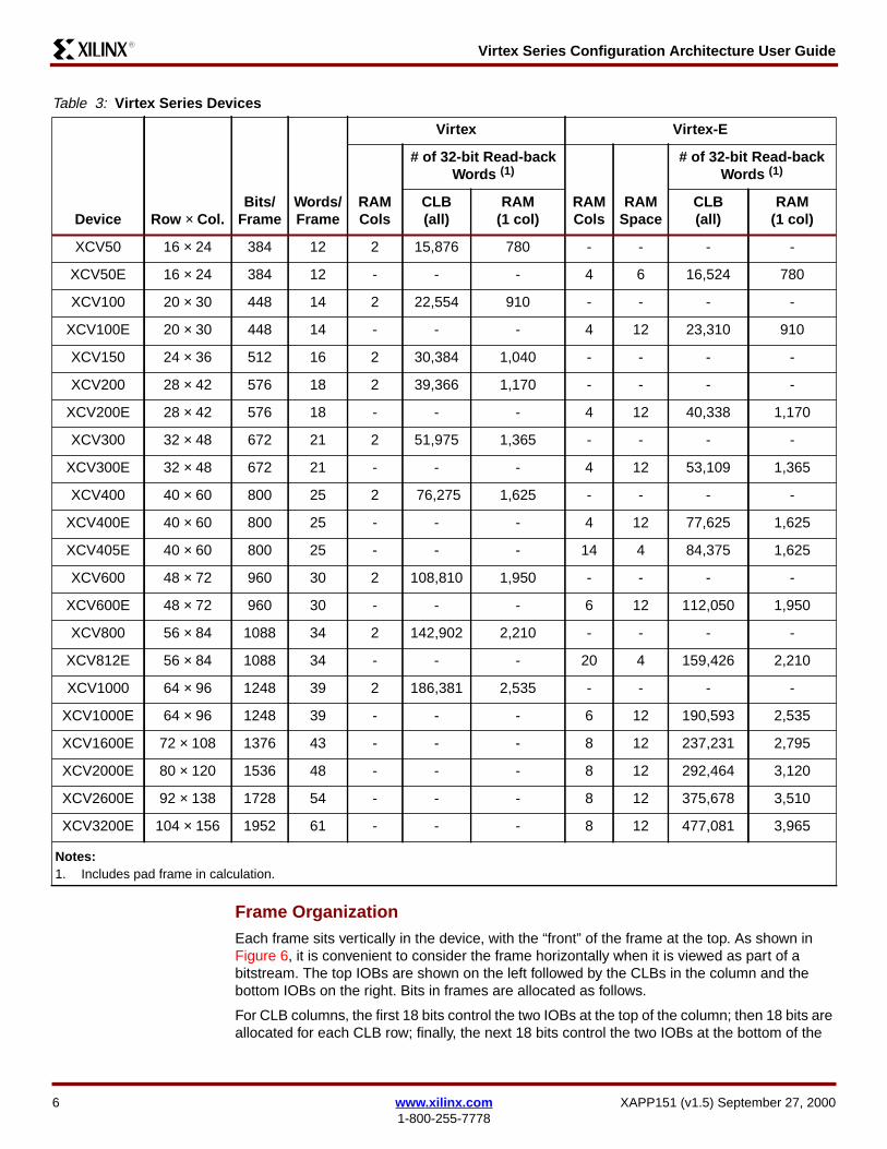
Virtex Series Configuration Architecture User GuideR13
Frame OrganizationEach frame sits vertically in the device with the ldquofrontrdquo of the frame at the top As shown inFigure 6 it is convenient to consider the frame horizontally when it is viewed as part of abitstream The top IOBs are shown on the left followed by the CLBs in the column and thebottom IOBs on the right Bits in frames are allocated as follows
For CLB columns the first 18 bits control the two IOBs at the top of the column then 18 bits areallocated for each CLB row finally the next 18 bits control the two IOBs at the bottom of the
Table 3 Virtex Series Devices
Device Row times ColBits
FrameWordsFrame
Virtex Virtex-E
RAMCols
of 32-bit Read-backWords (1)
RAMCols
RAMSpace
of 32-bit Read-backWords (1)
CLB(all)
RAM(1 col)
CLB(all)
RAM(1 col)
XCV50 16 times 24 384 12 2 15876 780 - - - -
XCV50E 16 times 24 384 12 - - - 4 6 16524 780
XCV100 20 times 30 448 14 2 22554 910 - - - -
XCV100E 20 times 30 448 14 - - - 4 12 23310 910
XCV150 24 times 36 512 16 2 30384 1040 - - - -
XCV200 28 times 42 576 18 2 39366 1170 - - - -
XCV200E 28 times 42 576 18 - - - 4 12 40338 1170
XCV300 32 times 48 672 21 2 51975 1365 - - - -
XCV300E 32 times 48 672 21 - - - 4 12 53109 1365
XCV400 40 times 60 800 25 2 76275 1625 - - - -
XCV400E 40 times 60 800 25 - - - 4 12 77625 1625
XCV405E 40 times 60 800 25 - - - 14 4 84375 1625
XCV600 48 times 72 960 30 2 108810 1950 - - - -
XCV600E 48 times 72 960 30 - - - 6 12 112050 1950
XCV800 56 times 84 1088 34 2 142902 2210 - - - -
XCV812E 56 times 84 1088 34 - - - 20 4 159426 2210
XCV1000 64 times 96 1248 39 2 186381 2535 - - - -
XCV1000E 64 times 96 1248 39 - - - 6 12 190593 2535
XCV1600E 72 times 108 1376 43 - - - 8 12 237231 2795
XCV2000E 80 times 120 1536 48 - - - 8 12 292464 3120
XCV2600E 92 times 138 1728 54 - - - 8 12 375678 3510
XCV3200E 104 times 156 1952 61 - - - 8 12 477081 3965
Notes1 Includes pad frame in calculation
6 wwwxilinxcom XAPP151 (v15) September 27 20001-800-255-7778
Virtex Series Configuration Architecture User GuideR13
CLB column The frame then contains enough ldquopadrdquo bits to make it an integral multiple of 32bits
For IOB columns the frame allocates 18 bits per three IOB rows Figure 7 When reading andwriting frames bits are grouped into 32-bit words starting on the left (corresponding to the topof the device) If the last word does not completely fill a 32-bit word it is padded on the right withzeroes
For block SelectRAM content columns (Figure 8) the first 18 bits are pad bits then 72 bits areallocated for each RAM row finally there are another 18 pad bits The frame then adds enoughldquopadrdquo bits to make it an integral multiple of 32 bits
Location of LUT SelectRAM BitsWith respect to the beginning of a configuration frame relative locations of LUT SelectRAM bitswithin the bitstream are the same for every CLB slice The bits of a LUT SelectRAM are spreadacross 16 consecutive frame Minor Addresses Each frame Minor Address contains allinstances of a single bit index for that column These 16 frames contain all 16 bits of the LUTSelectRAM for a column of CLB slices You must read or write the 16 frames containing thosebits to read or write the entire LUT SelectRAM
Figure 6 CLB Column Frame Organization
Figure 7 IOB Column Frame Organization
Figure 8 Block SelectRAM Content Column Frame Organization
Note LUT SelectRAM bits are stored inverted Flip-Flop data are stored in their true senseWhen reading or writing LUT SelectRAM data from the bitstream it is negated from the logicsense of the data For example a 4-input AND gate has the truth tableLUT[150] = 1000000000000000
This truth table isstored internally in theLUTSelectRAMasLUT[150] = 0111111111111111Ofcourse user logic reading the data from the LUT SelectRAM would read the correct logicvalue LUT[150] = 1000000000000000
Top 2 IOBs13 Bottom 2 IOBs1313
CLB Rn1313
13 18131813181318131813
CLB R213CLB R113
x151_06_020700
Top 3 IOBs Bottom 3 IOBs1313
181818
3 IOBs
x151_07_020800
Pad PadRAM Rn
1872727218
RAM R1RAM R0
x151_08_021800
XAPP151 (v15) September 27 2000 wwwxilinxcom 71-800-255-7778
Virtex Series Configuration Architecture User GuideR13
ConfigurationData Operations
Reading Configuration DataConfiguration information can be read from the Virtex devices if readback is enabled in thecurrent configuration (See the description of the Control Register field SBITS on page 21)CLB and IOB configuration data can be read while the device is operating
When reading data from a Virtex device a pad frame is read before any of the data framesThis is in addition to the pad word in each data frame The pad frame must be included in theword count to be read from the device
Each frame read from the device consists of the number of words shown in Table 3
For example the XCV150 has 16-word frames When reading frames the first word of a frameis a pad word Including the pad frame the XCV150 has 1899 (3038416) frames (SeeFigure 9)
Writing Configuration DataConfiguration information can be written to a Virtex device while the device is running if writingis enabled in the current configuration (See the Control Register field SBITS in Table 23) Re-writing the same configuration data does not generate any transient signals
Changing configuration data may generate transient signals especially if LUT values or signalrouting is changed For this case all the logic cells and routing can be placed in a non-contentious state by asserting the GHIGH_B signal See the description for the CommandRegister (CMD) on page 18
When writing configuration data to the Virtex device whether from the SelectMAP or JTAGinterfaces the data frames are written to the device with each frame followed by a pad wordAfter all the data frames are written a pad frame must be written (to flush internal pipelines)The pad words and pad frame must be included in the number of words to be written to thedevice (Table 3)
For example the XCV1000 has 39-word frames When writing frames the last word of theframe is a pad word Including the pad frame the XCV1000 has 4779 (18638139) framesSee Figure 10)
Altering Configuration DataVirtex devices support the Read-Modify-Write (RMW) method of changing LUT SelectRAMdata Therefore it is possible to read or alter the contents of one or more LUT SelectRAMsthrough the JTAG or SelectMAP interfaces When writing data to one or more LUTSelectRAMs all the bits in the frame must have valid configuration information This can beassured by altering valid configurations from bitstream files or from frames read from a properlyconfigured Virtex device When using the RMW method it may be expeditious to read the dataignoring the pad frame and the pad word of only the first frame This aligns the remaining
Pad Frame (16 words)Pad Word Data Frame 0 (15 words)
hellip
hellip
Pad Word Data Frame n (15 words)
Figure 9 XCV150 Frame Padding for Device Read
Data Frame 0 (38 words) Pad Word
hellip
Data Frame n (38 words) Pad WordPad Frame (39 words)
Figure 10 XCV1000 Frame Padding for Device Write
8 wwwxilinxcom XAPP151 (v15) September 27 20001-800-255-7778
Virtex Series Configuration Architecture User GuideR13
configuration data in the Device Write format After modifying the configuration the altered datacan be written to the Virtex device followed by a pad word and a pad frame
It is not necessary to retain the contents of the pad frame or pad words However pad wordsand pad frames are included in the CRC calculation
Definitions Two sets of variables are defined to determine where a desired bit is in the configuration dataThe first is a set of ldquoindependentrdquo variables or design attributes namely characteristics of thedesign that are known ie the device size and which CLB and bit(s) within the CLB to locateTable 4 The second set is a set of ldquodependentrdquo variables or design variables namely valuesthat must be calculated to find the bit(s) of interest listed in Table 5
Note Frames span an entire column of CLB slices (or IOBs) Thus when changing LUTSelectRAM bit 0 for a single CLB slice (eg R3C4S1) LUT SelectRAM bit 0 for all slices inthat column (ie RC4S1) is written with the same command One must ensure that either allother data in the slice is constant or changed externally through partial configurations
LUT SelectRAMs not configured externally should not lie in the same slice with LUTs or LUTSelectRAMs that are re-configured externally Such a mixture can cause the unrelated LUTSelectRAM data to be re-configured when the frames are written to the device Figure 11shows what can happen if this restriction is not observed
In this example it is the objective to perform a Read-Modify-Write on the LUT SelectRAM inR2C3S1 in column 3 which is shown in the first column in the figure Row 2 contains a LUTcontaining the value AB Row 3 contains a SelectRAM containing the value C3 Because theRead and Write operations operate on an entire frame the RAM in R3C3S1 is also read andwritten when R2C3S1 is read and written Performing the Readback operation reads all theLUT and SelectRAM values for the column Before the new value for the LUT is written it ispossible for the on-chip circuitry to write a new value such as 14 into the SelectRAM Whenthe new value BD is written via the configuration interface into LUT R2C3S1 the value C3 isalso written into RAM R3C3S1 This may not always be desirable (It is design-dependent)
Figure 11 Potential Write Conflicts
x151_11_020800
LUT R2C3S113AB13
RAM R3C3S113C313
Before13Readback
13
LUT R2C3S113AB13
RAM R3C3S1131413
Before13Configuration 13
Write
13
LUT R2C3S113BD13
RAM R3C3S113C313
After13Configuration13
Write
13
Table 4 Design Attributes (Independent Variables)
Term Definition
Chip_Cols of CLB columns on the Virtex device
Chip_Rows of CLB rows on the Virtex device
Chip_Rams of block SelectRAM columns on the Virtex device
RAM_Space Spacing of block SelectRAM columns (in terms of CLB columns)
FL of 32-bit words in the frame
XAPP151 (v15) September 27 2000 wwwxilinxcom 91-800-255-7778
Virtex Series Configuration Architecture User GuideR13
RW 1 for Read 0 for Write
CLB_Col Column number of the desired CLB
CLB_Row Row number of the desired CLB
Slice 0 or 1
FG 0 for the F-LUT 1 for the G-LUT
lut_bit The desired bit from the given LUT Bits in the LUT are indexed from 0 to 15
XY 0 for the X Flip-Flop 1 for the Y Flip-Flop
RAM_Col Column number of the desired block SelectRAM
RAM_Row Row number of the desired block SelectRAM
ram_bit The desired bit from the given block SelectRAM Bits are indexed from 0 to4095
Table 5 Design Variables (Dependent Variables)
Term Definition
MJA Frame Major Address
MNA Frame Minor Address
fm_st_wd The index of the word within a full configuration segment that correspondsto the starting word of the desired frame A full configuration segment isdefined as the following 1) for CLBIOB all CLB IOB and RAMinterconnect frames beginning at MJA=0 MNA=0 and 2) for blockSelectRAM all RAM content frames for the given RAM column Words arenumbered starting at 0
fm_wd The index of the 32-bit word within a frame that contains the desired bitWords in a frame are numbered starting at 0
fm_wd_bit_idx The bit index of the desired bit within frame word fm_wd Words areindexed in ldquobig-endianrdquo style with bit 31 on the left and bit 0 on the right
fm_bit_idx Bit index within a frame of the desired bit Numbered starting with 0 as theleft-most (first) bit Bit numbering within a frame continues across all thewords in the frame
Table 6 Functions used in Equations
Functions Definition
floor(x) The largest integer not larger than x Eg floor(31) = 3 because the nextlargest integer 4 is larger than 31 floor(3)=3
ceiling(x) The smallest integer greater than or equal to x For example ceiling(32) = 4because 4 is greater than 32 and 3 is not ceiling (4) = 4
The modulus operation 5 2 = 1 5 3 = 2 5 5 = 0
Table 4 Design Attributes (Independent Variables) (Continued)
Term Definition
10 wwwxilinxcom XAPP151 (v15) September 27 20001-800-255-7778
Virtex Series Configuration Architecture User GuideR13
CLB LUTSelectRAMDependentVariables
Table 7 shows equations for the LUT SelectRAM ldquoDependent Variablesrdquo that were defined inTable 5
Virtex-E CLB LUT SelectRAM Dependent VariablesThe additional block SelectRAM columns in Virtex-E devices require an adjustment to the MJAThe following equations calculate the adjustment necessary for each of the affected dependentvariables For each variable calculate the base value based upon the Virtex equations onlyand then add the resulting Virtex adjustment
The left and right sides of the device are treated differently
LUT SelectRAM ExamplesSee ldquoExamplesrdquo on page 27 for several examples of reading and evaluating configuration dataThe examples illustrate how to make use of these equations to find the desired data in abitstream
Table 7 Virtex Equations for LUT SelectRAM Dependent Variables
Term Definition
MJA if (CLB_Col le Chip_Cols2)then Chip_Cols ndash CLB_Col times 2 + 2else 2 times CLB_Col ndash Chip_Cols ndash 1
MNA lut_bit + 32 ndash Slice times (2 times lut_bit + 17)
fm_bit_idx 3 + 18 times CLB_Row ndash FG + RW times 32
fm_st_wd FL times (8 + (MJA ndash1) times 48 + MNA) + RW times FL
fm_wd floor(fm_bit_idx32)
fm_wd_bit_idx 31 + 32 times fm_wd ndash fm_bit_idx
Notes
bull Do NOT input the final results back into the original Virtex equations (eg do not useMJAfinal value to calculate fm_st_wd)
bull MJAfinal = MJA + MJA_adj
bull fm_st_wdfinal = fm_st_wd + fm_st_wd_adj
Table 8 CLB Location
CLB Location CLB Column
Left CLB_Col le Chip_Cols2
Right CLB_Col gt Chip_Cols2
Table 9 Virtex-E Families Adjustments for LUT SelectRAM Dependent Variables
Term Definition
MJA_adj Left RAM_Bound = (Chip_Rams2 - 1) x RAM_SpaceMJA_adj = 2 x ceiling((RAM_Bound - CLB_Col + 1) RAM_Space)
Right
RAM_Bound = Chip_Cols - (Chip_Rams2 - 1) x RAM_Space + 1MJA_adj = 2 x ceiling((CLB_Col - RAM_Bound + 1) RAM_Space)
fm_st_wd_adj FL times (27 x MJA_adj)
XAPP151 (v15) September 27 2000 wwwxilinxcom 111-800-255-7778
Virtex Series Configuration Architecture User GuideR13
CLB Flip-FlopDependentVariables
Equations for the CLB flip-flops can be found in Table 10 Their locations are calculatedsimilarly to the LUT SelectRAM locations Equations for the CLB FF Dependent Variables aredefined in Table 5
Virtex-E CLB Flip-Flop Dependent VariablesApply the adjustments given in Table 8 and Table 9
IOB DependentVariables
Each IOB contains four values that can be captured into special registers These values are
bull I mdash the input flip-flop
bull O mdash the output flip-flop
bull T mdash the flip-flop for the tri-state control
bull P mdash the value of the IO pad
These values are captured by utilizing the CAPTURE_VIRTEX symbol in your design TheLibraries Guide has more details on the use of this symbol The following registers will be readas part of the readback data
Access to the IOB flip-flops is different for the top and bottom IOBs versus the left and rightIOBs
The top and bottom IOBs are part of the CLB column frames There are two IOBs at the top andbottom of each CLB column
The left and right IOBs are in columns by themselves There are three IOBs per CLB row
IOBs are numbered clockwise around the die Pad 1 is located at the left side of the top edgeabove CLB column 1 The equations for where to find IOB flip-flops in the bitstream are basedon the pad number which is the same for a given size device not the package pin name whichvaries from package to package The mapping from package pin names to pad numbers canbe found in EPIC or fpga_editor
Table 11 contains the numeric pad indices for the pads on all four edges of the device in termsof the number of CLB columns and rows on the device
Table 10 Virtex Equations for CLB FF Dependent Variables
Term Definition
MJA if (CLB_Col le Chip_Cols2)then Chip_Cols ndash CLB_Col times 2 + 2else 2 times CLB_Col ndash Chip_Cols ndash 1
MNA Slice times (12 times XY ndash 43) ndash 6 times XY + 45
fm_bit_idx (18 times CLB_Row) + 1 + (32 times RW)
fm_st_wd FL times (8 + (MJA ndash1) times 48 + MNA) + RW times FL
fm_wd floor(fm_bit_idx32)
fm_wd_bit_idx 31 + 32 times fm_wd ndash fm_bit_idx
12 wwwxilinxcom XAPP151 (v15) September 27 20001-800-255-7778
Virtex Series Configuration Architecture User GuideR13
Table 12 shows the equations for the dependent variables for the IOB flip-flops The variable iin this table refers to the index of pad i
Table 11 IOB Pad Indices
PadLocation Pad Index i
Top 1 le i le Chip_Cols times 2
Right Chip_Cols times 2 +1 le i le Chip_Cols times 2 + Chip_Rows times 3
Bottom Chip_Cols times 2 + Chip_Rows times 3 + 1 le i le Chip_Cols times 4 + Chip_Rows times 3
Left Chip_Cols times 4 + Chip_Rows times 3 + 1 le i le Chip_Cols times 4 + Chip_Rows times 6
Table 12 Equations for IOB Dependent Variables
Term Definition
MJA
Topif (i le Chip_Cols)then Chip_Cols ndash ceiling(i2) times 2 + 2else 2 times ceiling (i2) ndash Chip_Cols ndash1
Right Chip_Cols + 1
Bottomif (i gt 3 times (Chip_Cols + Chip_Rows))then 2 times ceiling((i ndash 3 times Chip_Cols ndash 3 times Chip_Rows)2)else Chip_Cols ndash 2 times floor((i ndash 2 times Chip_Cols ndash 3 times Chip_Rows ndash 1)2) ndash 1
Left Chip_Cols + 2
MNA
Top
I ndash 25 times (i2) + 45
O ndash 13 times (i2) + 39
T ndash 5 times (i2) + 35
P ndash 4 times (i2) + 25
Right
I t = (i ndash 2 times Chip_Cols) 3 MNA = 275 times t2 ndash 575 times t + 32
O t = (i ndash 2 times Chip_Cols) 3 MNA = 215 times t2 ndash 515 times t + 38
T t = (i ndash 2 times Chip_Cols) 3 MNA = 175 times t2 ndash 475 times t + 42
P 50
Bottom
I 25 times ((i ndash 2 x Chip_Cols - 3 x Chip_Rows)2) + 20
O 13 times ((i ndash 2 x Chip_Cols - 3 x Chip_Rows)2) + 26
T 5 times ((i ndash 2 x Chip_Cols - 3 x Chip_Rows)2) + 30
P 4 times ((i ndash 2 x Chip_Cols - 3 x Chip_Rows)2) + 21
Left
I t = (i ndash 4 x Chip_Cols - 3 x Chip_Rows)3 MNA = 175 times t2 ndash 475 times t + 45
O t = (i ndash 4 x Chip_Cols - 3 x Chip_Rows)3 MNA = 235 times t2 ndash 535 times t + 39
T t = (i ndash 4 x Chip_Cols - 3 x Chip_Rows)3 MNA = 275 times t2 ndash 575 times t + 35
P 50
XAPP151 (v15) September 27 2000 wwwxilinxcom 131-800-255-7778
Virtex Series Configuration Architecture User GuideR13
Virtex-E IOB Dependent VariablesSimilar to CLB dependent variables only the variables affected by the major address aredifferent in Virtex-E and Virtex-EM devices versus Virtex devices A simple way to account forthe change is to determine the CLB column where the pad resides (only true for top andbottom) Then the adjustment calculated for the CLB column can be applied The conversionto CLB columns is found in Table 13
fm_bit_idx
Top 32 times RW
Right
I O ampT 18 times (1 + floor ((i ndash 2 times Chip_Cols ndash 1)3)) + 32 times RW
Pt = (i ndash 2 times Chip_Cols) 3fm_bit_idx = 18 times (1 + floor ((i ndash 2 times Chip_Cols ndash 1)3)) + 6 times t2 ndash 17 times t + 15 + 32 timesRW
Bottom 18 times (Chip_Rows + 1)+ 32 times RW
Left
I O ampT18 times (Chip_Rows ndash floor((i ndash 4 times Chip_Cols ndash 3 times Chip_Rows ndash 1)3)) + 32 times RW
Pt = (i ndash 4 times Chip_Cols ndash 3 times Chip_Rows)3fm_bit_idx = 18 times (Chip_Rows ndash floor ((i ndash 4 times Chip_Cols ndash 3 times Chip_Rows ndash 1)3))ndash 105 times t2 + 215 times t + 4 + 32 times RW
fm_st_wdif (MJA gt Chip_Cols + 1)then FL times (54 times MJA ndash 46 + MNA ndash 6 times Chip_Cols) + RW times FLelse FL times (8 + (MJA ndash1) times 48 + MNA) + RW times FL
fm_wd floor (fm_bit_idx32)
fm_wd_bit_idx 31 + 32 times fm_wd ndash fm_bit_idx
Table 12 Equations for IOB Dependent Variables (Continued)
Term Definition
Table 13 Pad -gt CLB Column
Term Definition
CLB_ColTop ceiling(i2)
Bottom ceiling((4 x Chip_Cols + 3 x Chip_Rows + 1 - i)2)
Table 14 Virtex-E Families Adjustments for IOB Dependent Variables
Term Definition
MJA_adj
Top use Table 8 and Table 9
Right Chip_Rams
Bottom use Table 8 and Table 9
Left Chip_Rams
fm_st_wd_adj FL times (27 x MJA_adj)
14 wwwxilinxcom XAPP151 (v15) September 27 20001-800-255-7778
Virtex Series Configuration Architecture User GuideR13
BlockSelectRAMDependentVariables
The equations for the block SelectRAM dependent variables are given in Table 15 Therelationship of a particular memory cell index in the context of a given configuration is describedin XAPP130 ldquoUsing the Vir tex Bloc k SelectRAM+ Resour cerdquo
Virtex-E Block SelectRAM Dependent VariablesThe RAM major address numbering scheme changed slightly such that the lowest MJA on theleft side is now 2 instead of 0 As in the case for the CLB equations the adjustments belowshould be applied after the Virtex equations
Table 15 Virtex Equations for Block SelectRAM Dependent Variables
Term Definition
MJAif (RAM_Col lt Chip_Rams2)then 2 x (Chip_Rams2 - 1 - RAM_Col)else 2 x (RAM_Col - Chip_Rams2) + 1
MNA
1 x floor(((ram_bit 64) 64)32) + 2 x floor(((ram_bit 64) 32)16)+ 4 x floor(((ram_bit 64) 16)8) + 8 x floor(((ram_bit 64) 8)4)+ 16 x floor(((ram_bit 64) 4)2) + 32 x floor(((ram_bit 64) 2)1)equivalent to MNA = div64[05] where div64[50] = floor(ram_bit64)
fm_bit_idxobtain value for bitpos from Table 16
fm_bit_idx = 18 + 72 x RAM_Row + bitpos
fm_st_wd FL times MNA + RW times FL
fm_wd floor(fm_bit_idx32)
fm_wd_bit_idx 31 + 32 times fm_wd ndash fm_bit_idx
Table 16 Virtex Block SelectRAM Bit Position Within a Given Block SelectRAM
ram
_bit
6
4
bitp
os
ram
_bit
6
4
bitp
os
ram
_bit
6
4
bitp
os
ram
_bit
6
4
bitp
os
ram
_bit
6
4
bitp
os
ram
_bit
6
4
bitp
os
ram
_bit
6
4
bitp
os
ram
_bit
6
4
bitp
os
0 42 8 45 16 29 24 26 32 43 40 44 48 28 56 27
1 58 9 61 17 13 25 10 33 59 41 60 49 12 57 11
2 41 10 46 18 30 26 25 34 40 42 47 50 31 58 24
3 57 11 62 19 14 27 9 35 56 43 63 51 15 59 8
4 50 12 53 20 21 28 18 36 51 44 52 52 20 60 19
5 49 13 54 21 22 29 17 37 48 45 55 53 23 61 16
6 66 14 69 22 5 30 2 38 67 46 68 54 4 62 3
7 65 15 70 23 6 31 1 39 64 47 71 55 7 63 0
Table 17 Virtex-E and Virtex-EM Adjustments for Block SelectRAM DependentVariables
Term Definition
MJA_adj if (RAM_Col lt Chip_Rams2) MJA_adj = 2
XAPP151 (v15) September 27 2000 wwwxilinxcom 151-800-255-7778
Virtex Series Configuration Architecture User GuideR13
ConfigurationLogic Basics
Configuration DataConfiguration data is organized as 32-bit words There are two major commands that theconfiguration data can contain Read and Write A configuration command is executed whenthe configuration command is read or written to the appropriate command register
The OP field contains 01 for a Read operation and 10 for a Write operation (See Figure 12)
A command is organized as a packet with a header word and optional data words The headerword is the first word written to the appropriate command register for a read or write operationThe header word contains a type field (001) an operand field a register address field and aword count field The format for the command header is shown in Figure 13 on page 17
The Register Address field defines the target of this command as defined in Table 18 on page17
The header word count field contains an integer between 0 and 2047 and indicates thenumber of words that follow the header Larger word counts (between 2048 and 1048575words) are achieved by setting the header word count to 0 The Extension header word has atype field = 010 an OP field that must match the OP field in the preceding Command Headerword and a 20-bit word count this format is shown Figure 14 on page 17
Configuration FlowVirtex devices are configured by presenting configuration data to the SelectMAP or JTAGinterfaces in a specific sequence
For Initial Configuration
1 Issue one or more pad words (SelectMAP only)
2 Issue Sync word (SelectMAP only)
3 Reset CRC
4 Set FLR
5 Set COR
6 Set MASK
7 Set CTL (Set PERSIST if you want to keep SelectMAP active after this configuration)
8 Issue a SWITCH (switch CCLK frequency) command to the CMD register This isnecessary only in Master Serial configuration mode
Reading Configuration
These commands can be issued to read a full configuration or for a partial configuration afterthe device has been completely configured
1 Issue a Sync word (SelectMAP only) if the previous configuration command was aborted
2 Set the FAR to the starting address
3 Issue a RCFG (read configuration) command to the CMD register
4 Write the number of words to be read to the FDRO register
5 Flush the command pipeline with a pad word
6 Read data frames
OP CODERead 01Write 10
Figure 12 OP Field Code
16 wwwxilinxcom XAPP151 (v15) September 27 20001-800-255-7778
Virtex Series Configuration Architecture User GuideR13
Writing Configuration
These commands can be issued either as part of an initial configuration or for a partialconfiguration after the device has been configured
1 Issue a Sync word (SelectMAP only) if the previous configuration command was aborted
2 If the frames being written can cause contention then assert the GHIGH_B signal
3 Set the FAR to the starting address
4 Issue a WCFG (write configuration) command to the CMD register
5 Write the number of words to be written to the FDRI register
6 Write data frames
7 If the GHIGH_B signal was asserted de-assert it by writing the LFRM (Last Frame)command to the CMD register and write one pad frame
ConfigurationRegisters
Configuration logic is accessed and controlled via a collection of 32-bit registers called theconfiguration registers (see Table 18) Registers are described in the following sections
Type OP Register Address RSV Word Count31 30 29 28 27 26 25 24 23 22 21 20 19 18 17 16 15 14 13 12 11 10 9 8 7 6 5 4 3 2 1 00 0 1 x x 0 0 0 0 0 0 0 0 0 0 x x x x 0 0 x x x x x x x x x x x
Notes1 Locations within fields containing a zero or one must have these values An X in a bit field indicates that the value is variable and must
be set2 Heavy vertical lines are used to separate fields Light vertical lines separate nibbles in the word
Figure 13 Command Header Format
Type OP Word Count31 30 29 28 27 26 25 24 23 22 21 20 19 18 17 16 15 14 13 12 11 10 9 8 7 6 5 4 3 2 1 00 1 0 x x 0 0 0 0 0 0 0 x x x x x x x x x x x x x x x x x x x x
Notes1 Locations within fields containing a zero or one must have these values An X in a bit field indicates that the value is variable and must
be set2 Heavy vertical lines are used to separate fields Light vertical lines separate nibbles in the word
Figure 14 Large Block Count Header Extension Format
Table 18 Configuration Register Addresses
Register Name Mnemonic RW Binary Address
CRC CRC RW 0000
Frame Address FAR RW 0001
Frame Data Input FDRI W 0010
Frame Data Output FDRO R 0011
Command CMD RW 0100
Control CTL RW 0101
Control Mask MASK RW 0110
Status STAT R 0111
Legacy Output LOUT W 1000
XAPP151 (v15) September 27 2000 wwwxilinxcom 171-800-255-7778
Virtex Series Configuration Architecture User GuideR13
Command Register (CMD)The content of the Command Register (CMD) is interpreted by the configuration state machineConfiguration commands control the operation of the configuration state machine the FrameData Register (FDR) and some of the global signals The command in the Command Registeris executed each time the FAR is loaded with a new value The effect of each command isdefined in Table 19
Configuration Option COR RW 1001
Reserved mdash mdash 1010
Frame Length FLR RW 1011
Reserved mdash mdash 1100
Reserved mdash mdash 1101
Reserved mdash mdash 1110
Reserved mdash mdash 1111
Table 18 Configuration Register Addresses (Continued)
Register Name Mnemonic RW Binary Address
Table 19 Configuration Commands
Cmd Code Description
Rsvd 0000 Reserved
WCFG 0001Write Configuration Data mdash Used prior to writing configuration data to the FDRI It takes theinternal configuration state machine through a sequence of states that control the shifting of the FDRand the writing of the configuration memory (See Frame Data Input Register (FDRI) on page 24)
Rsvd 0010 Reserved
LFRM 0011Last Frame mdash This command is loaded prior to writing the last (pad) data frame if the GHIGH_Bsignal was asserted This command is not necessary if the GHIGH_B signal was not asserted Thisallows overlap of the last frame write with the release of the GHIGH_B signal
RCFG 0100Read Configuration Data mdash Used prior to reading frame data from the FDRO Similar to the WCFGcommand in its effect on the FDR (see Frame Data Output Register (FDRO) on page 24)
START 0101Begin Startup Sequence mdash Starts the startup sequence This command is also used to start ashutdown sequence prior to partial re-configuration The Startup Sequence begins with the nextsuccessful CRC check (see Cyclic Redundancy Check (CRC) on page 22)
RCAP 0110Reset Capture mdash Used when performing capture in single-shot mode This command must be usedto reset the capture signal if single-shot capture has been selected
RCRC 0111 Reset CRC mdash Used to reset CRC register (see Cyclic Redundancy Check (CRC) on page 22)
AGHIGH 1000Assert GHIGH_B Signal mdash Used prior to re-configuration to prevent contention while writing newconfiguration data All CLB outputs and signals are forced to a one
SWITCH 1001Switch CCLK Frequency mdash Used to change (increase) the frequency of the Master CCLK Thenew frequency is specified in Table 21
Rsvd 1010 Reserved
Rsvd 1011 Reserved
Rsvd 1100 Reserved
18 wwwxilinxcom XAPP151 (v15) September 27 20001-800-255-7778
Virtex Series Configuration Architecture User GuideR13
Configuration Option Register (COR)The Configuration Option Register (COR) is used to select configuration options that areillustrated in Figure 15 and defined in Table 20 Entries in this table are further explained in thefollowing tables
Rsvd 1101 Reserved
Rsvd 1110 Reserved
Rsvd 1111 Reserved
Table 19 Configuration Commands (Continued)
Cmd Code Description
DO
NE
_PIP
E
DR
IVE
_DO
NE
SIN
GLE
OS
CF
SE
L
SS
CLK
SR
C
LOC
K_W
AIT
SH
UT
DO
WN
DO
NE
_CY
CLE
LCK
_CY
CLE
GT
S_C
YC
LE
GW
E_C
YC
LE
GS
R_C
YC
LE
31 30 29 28 27 26 25 24 23 22 21 20 19 18 17 16 15 14 13 12 11 10 9 8 7 6 5 4 3 2 1 00 x x x x x x x x x x x x x x x x x x x x x x x x x x x x x x x
Notes1 Locations within fields containing a zero or one must have these values An X in a bit field indicates that the value is variable and must
be set2 Heavy vertical lines are used to separate fields Light vertical lines separate nibbles in the word
Figure 15 COR (Configuration of Option Register) Fields
XAPP151 (v15) September 27 2000 wwwxilinxcom 191-800-255-7778
Virtex Series Configuration Architecture User GuideR13
Table 21 shows the allowed values for the OSCFSEL field of the COR Setting OSCFSEL toone of these values will set the Master CCLK frequency to the specified value
Table 20 Configuration Option Register Fields
Field Bit Indices DescriptionBitgenDefault
DONE_PIPE 30
0 No pipeline stage for DONEIN
1 Add pipeline stage to DONEINFPGA waits on DONE that is delayed by one (1) cycle of the StartupClkrather than the pin itself Use this option when StartupClk is running at highspeeds
0
DRIVE_DONE 290 DONE pin is open drain
1 DONE pin is actively driven high0
SINGLE 28 Readback capture is one-shot 0
OSCFSEL 2722 Select CCLK frequency in Master Serial configuration mode 2
SSCLKSRC 2120
Startup sequence clock source00 Cclk01 UserClk1x JTAGClk
0
LOCK_WAIT 1916
4-bit mask indicating which DLL lock signals to wait for during LCK cycleThe 4 bits (from MSB to LSB) correspond to DLLs TL=3 TR=2 BL=1BR=0 (top-left top-right etc) In Virtex-E devices where there are 8 DLLseach mask bit applies to the 2 DLLs in that quadrant of the device Thedefault is not to wait for any DLL lock signals
0
SHUTDOWN 15
Indicate whether doing a startup or shutdown sequence
0 Startup
1 Shutdown sequence
0
DONE_CYCLE 1412 Startup phase in which DONE pin is released 3
LCK_CYCLE 119 Stall in this startup phase until DLL locks are asserted 7
GTS_CYCLE 86 Startup phase in which IOs switch from tri-state to user design 4
GWE_CYCLE 53 Startup phase in which the global write-enable is asserted 5
GSR_CYCLE 20 Startup phase in which the global setreset is negated 5
Table 21 OSCFSEL-Specified Master CCLK Frequencies)
CCLK(MHz) OSCFSEL
CCLK(MHz) OSCFSEL
CCLK(MHz) OSCFSEL
43 000010 13 001010 41 100111
54 010001 15 001101 45 110011
69 000100 20 010111 51 101010
81 000101 26 011010 55 110100
20 wwwxilinxcom XAPP151 (v15) September 27 20001-800-255-7778
Virtex Series Configuration Architecture User GuideR13
Table 22 shows the values of the DONE_CYCLE LCK_CYCLE GTS_CYCLE GWE_CYCLEand GSR_CYCLE fields in COR This table shows the step in the start-up sequence when eachof these signals becomes active
Control Register (CTL)The Control Register (CTL) fields are illustrated in Figure 16 on page 21 and defined inTable 23
92 000110 30 011101 60 101101
100 000111 34 110010 mdash mdash
Notes1 These values are accurate to +45 ndash 30
Table 22 COR Startup Cycle Fields
FieldValue
DONE_CYCLE(DONE Active)
GTS_CYCLE(GTS_CFGInactive)
GSR_CYCLE(GSR Inactive)
GWE_CYCLE(GWE Active) LCK_CYCLE
000 1 1 1 1 0
001 2 2 2 2 1
010 3 3 3 3 2
011 4 (default) 4 4 4 3
100 5 5 (default) 5 5 4
101 6 6 6 (default) 6 (default) 5
110 mdash DoneIndagger DoneIndagger DoneIndagger 6
111 Keep State Keep State Keep State Keep State Donrsquot Wait(default)
Notes1 dagger DONE if DonePipe = No else the delayed version of DONE
Table 21 OSCFSEL-Specified Master CCLK Frequencies) (Continued)
CCLK(MHz) OSCFSEL
CCLK(MHz) OSCFSEL
CCLK(MHz) OSCFSEL
SB
ITS
PE
RS
IST
GT
S_U
SR
_B
31 30 29 28 27 26 25 24 23 22 21 20 19 18 17 16 15 14 13 12 11 10 9 8 7 6 5 4 3 2 1 00 0 0 0 0 0 0 0 0 0 0 0 0 0 0 0 0 0 0 0 0 0 0 x x x 0 0 0 0 0 x
Notes1 Locations within fields containing a zero or one must have these values An X in a bit field indicates that the value is variable and must
be set2 Heavy vertical lines are used to separate fields Light vertical lines separate nibbles in the word
Figure 16 Control Register Fields
XAPP151 (v15) September 27 2000 wwwxilinxcom 211-800-255-7778
Virtex Series Configuration Architecture User GuideR13
Cyclic Redundancy Check (CRC)A data input error checking mechanism is provided through the Cyclic Redundancy Check(CRC) register When data is written to any configuration register (except LOUT) a 16-bit CRCvalue is calculated using both the register data and the address This value is saved in the CRCregister At the end of any series of writes a pre-calculated CRC block-check value may bewritten to the CRC register If the resulting value is non-zero an error is indicated TheCRC_ERROR bit is accessible through the status register If a CRC error is detectedconfiguration logic is put in the ERROR mode The following section is an algorithm forcomputing CRC
CRC Algorithm Initialization bcc = 0skip_pad = truemore_words = true Check for write operation do
w = next_wordif (w[3127] == rsquo00101rsquo)
A Read OP Donrsquot use in CRCwc = w[100]if (wc == 0)
w = next_wordwc = w[190]
while (wc-- gt 0)
w = next_word
elsif (w[3127] == rsquo00110rsquo)
A Write OP Use in CRC addr = w[1613]if (addr Π0124569DB)
wc = w[100]if (wc == 0)
wc is in next word w = next_wordwc = w[190]
while (wc-- gt 0)
w = next_wordsw[350] = addr wordfor (i=0 ilt36 i++)
Table 23 Control Register Bits
NameBit
Indices Description
SBITS 87 Security level0 ReadWrite OK (default)1 Readback disabled23 Readback disabled Writing disabled except CRCregister
PERSIST 6 Configuration interface remains after configuration0 No (default)1 Yes
GTS_USR_B 0 Active-low global tristate IOs Turn off pull-ups ifGTS_CFG_B is also asserted
22 wwwxilinxcom XAPP151 (v15) September 27 20001-800-255-7778
Virtex Series Configuration Architecture User GuideR13
x16 = bcc[15] XOR sw[i]x15 = bcc[14] XOR x16x2 = bcc[1] XOR x16bcc[150] =
x15bcc[132]x2bcc[0]x16 Note the bit order crc[150] = bcc[015]
else
Pad word - ignore
while (more_words)
Frame Address Register (FAR)The Frame Address Register (FAR) holds the address of the current frame The address isdivided into three parts the block type the major address and the minor address The blocktype field indicates whether the CLB or block RAM address space is used The command in thecommand register is executed each time the FAR is loaded with a new value
The major address selects the CLB or RAM column the minor address selects the frame withinthe column The minor address is incremented each time a full data frame is read from orwritten to the frame data register If the last frame within the CLB column is selected when theincrement occurs the major address is incremented and the minor address is reset to zerootherwise the minor address is incremented However the block RAM major address is notincremented automatically
See Figure 18 for the definitions of valid values for the block type field The FAR field definitionsare shown in Figure 19
Figure 17 CRC Calculation Register
Note the Block RAM Major Address is not incremented automatically To address a differentBlock RAM Content column the FAR must be loaded with the new Major Address
Type CodesCLB 00RAM 01
Figure 18 Block Type Codes
x151_17_021100
15141312111098765432
1013
01234526272829303101
Address 32-bit Data Word
CRC Calculation Register
CRC Data Input Register
CRC Register [310]
DATA_IN
SHIFT
23
16-bit CRC13150
0000 0000 0000 0000133116
1313
XAPP151 (v15) September 27 2000 wwwxilinxcom 231-800-255-7778
Virtex Series Configuration Architecture User GuideR13
Frame Data Input Register (FDRI)The Frame Data Input Register (FDRI) is used to load configuration frame data into a Virtexdevice
The Frame Data Register (FDR) is a shift register into which data is loaded prior to transfer tothe configuration memory Configuration data is written to the Virtex device by loading thecommand register with the WCFG command and then loading the FDR with at least two framesof 32-bit words
The write operation is pipelined such that the first frame of data is written to the configurationmemory while the second frame is being shifted in The last frame (the pad frame) is alwaysdummy data which is not actually written to the configuration memory Each frame write mustinclude enough 32 bit data words to load the frame fully There is one pad word at the end ofeach frame which is required for the pipelining hardware
Frame Data Output Register (FDRO)The Frame Data Output Register (FDRO) is for reading configuration data or captured datafrom the Virtex device a process called readback Readback is performed by loading thecommand register with the RCFG command and then addressing the FDRO with a readcommand
Frame Length Register (FLR)Near the beginning of the configuration bitstream the Frame Length Register (FLR) is writtenwith the length of a frame as measured in 32-bit words This length count is used to providesequencing information for the configuration read and write operations Note that the FLR mustbe written before any FDR operation works It is not necessary to set the FLR more than onceIf the number of bits in a frame is not evenly divisible by 32 the length count of the frame mustbe rounded up to the next highest integer The values for the FLR for all the current Virtexseries devices are given in Table 24
BlockType
Major Address(Column Address)
Minor Address(Frame Address)
31 30 29 28 27 26 25 24 23 22 21 20 19 18 17 16 15 14 13 12 11 10 9 8 7 6 5 4 3 2 1 00 0 0 0 0 x x x x x x x x x x x x x x x x x x 0 0 0 0 0 0 0 0 0
Notes1 Locations within fields containing a zero or one must have these values An X in a bit field indicates that the value is variable and must
be set2 Heavy vertical lines are used to separate fields Light vertical lines separate nibbles in the word
Figure 19 Frame Address Fields (FAR)
Note The FLR contains a value that is one less than the number of words that are read fromor written to a given frame This is because the extra word needed for pipelining is not counted
Table 24 Frame Length Register Value
Device Row times Col Frame Length Words per Frame FLR Value
XCV50E 16 times 24 384 12 11
XCV100E 20 times 30 448 14 13
XCV150 24 times 36 512 16 15
XCV200E 28 times 42 576 18 17
XCV300E 32 times 48 672 21 20
24 wwwxilinxcom XAPP151 (v15) September 27 20001-800-255-7778
Virtex Series Configuration Architecture User GuideR13
Legacy Output Register (LOUT)The Legacy Output Register (LOUT) is used for daisy chaining the configuration bitstream toother Xilinx devices Data written to the LOUT is serialized and appears on the DOUT pin
Mask Register (MASK)The Mask Register (MASK) is a mask register for writes to the CTL register A 1 in bit N of themask allows that bit position to be written in the CTL register The default value of the mask isall 0s
Status Register (STAT)The Status Register (STAT) is loaded with current values of several control or status signalsThe register can be read via the re-configuration block or via JTAG The fields in the Statusregister are illustrated in Figure 20 The values of the signals given in Table 25 on page 26 canbe read from the status register
XCV400E 40 times 60 800 25 24
XCV405E 40 times 60 800 25 24
XCV600E 48 times 72 960 30 29
XCV800 56 times 84 1088 34 33
XCV812E 56 times 84 1088 34 33
XCV1000E 64 times 96 1248 39 38
XCV1600E 72 times 108 1376 43 42
XCV2000E 80 times 120 1536 48 47
XCV2600E 92 times 138 1728 54 53
XCV3200E 104 times 156 1952 61 60
Table 24 Frame Length Register Value (Continued)
Device Row times Col Frame Length Words per Frame FLR Value
DO
NE
INIT
MO
DE
GH
IGH
_B
GS
R_B
GW
E_B
GT
S_C
FG
IN_E
RR
OR
LOC
K
CR
C_E
RR
OR
31 30 29 28 27 26 25 24 23 22 21 20 19 18 17 16 15 14 13 12 11 10 9 8 7 6 5 4 3 2 1 00 0 0 0 0 0 0 0 0 0 0 0 0 0 0 0 0 x x x x x x x x x x x x x x x
Notes1 An X in a bit field indicates that the value is variable2 Heavy vertical lines are used to separate fields Light vertical lines separate nibbles in the word
Figure 20 Status Register Fields
XAPP151 (v15) September 27 2000 wwwxilinxcom 251-800-255-7778
Virtex Series Configuration Architecture User GuideR13
ConfigurationInterface
There are two configuration interfaces to the Virtex devices mdash the bit-serial Boundary Scaninterface and the 8-bit byte-serial SelectMAP interface Conceptually XCV50 configurationdata appears as in Figure 21
Frames and words within frames are written in the same order in both configuration interfacesstarting with Frame 0 word 0 (the left-most in the picture) followed by word 1 etc Bits withineach word are written from left to right (MSB first) in the bit-serial configuration interfaces
Within the SelectMAP interface data is written a byte at a time A sample word is shown inFigure 22 The top row indicates the device pin names The bottom row indicates the bit indiceswithin a configuration word Byte 0 loads first followed by byte 1 et cetera The MSB of eachbyte (ie bits 31 23 15 and 7) is loaded on pin D0 The LSB of each byte (ie bits 24 16 8and 0) is loaded on pin D7
PartialReconfigurationof CLBs
Partial reconfiguration can be performed with and without shutting down the device Ifcontention occurs it is advised to go through a shutdown sequence prior to loadingconfiguration frames When shutting down the DONE pin will go active and pull low If this is notdesireable the DONE pin can be prevented from going low by selecting the DONE_CYCLE toKeep State (111) Similarly to prevent GSR from becoming active and reseting the currentstate the GSR_CYCLE can be set to Keep State When not shutting down changes occurframe by frame but is completely done by the end of the Last Frame packet (see Example 1)
Table 25 Status Register Bits
Name Bit Indices Description
DONE 14 Input from DONE pin
INIT 13 Value of INIT
MODE 1210 Value of M2 M1 M0 mode pins
GHIGH_B 9 0 = GHIGH_B asserted
GSR_B 8 0 = all flip-flops are ResetSet
GWE_B 7 1 = flip-flops and block RAM are write disabled
GTS_CFG 6 0 = IOs are tri-stated
IN_ERROR 5 Legacy input error
LOCK 41 Output from DLL lock signals 1 = DLL is locked
CRC_ERROR 0 Indicates that a CRC error has occurred
Data Frame 0 (11 words) Pad Word
hellip
Data Frame n (11 words) Pad WordPad Frame (12 words)
Figure 21 XCV50 Frame Padding for Reads
Figure 22 SelectMAP Byte and Bit Ordering
x151_22_021100
D0 D1 D2 D3 D4 D5 D6 D7 D0 D1 D2 D3 D4 D5 D6 D7 D0 D1 D2 D3 D4 D5 D6 D7 D0 D1 D2 D3 D4 D5 D6 D7
Byte 0 Byte 1 Byte 2 Byte 313
26 wwwxilinxcom XAPP151 (v15) September 27 20001-800-255-7778
Virtex Series Configuration Architecture User GuideR13
The DONE pin will not change in this case Figure 23 illustrates a typical shutdownreconfiguration in the CLB address space and restart sequence
Examples Several examples of reading and evaluating configuration data are provided to illustrate thefollowing
Figure 23 Typical Shutdown Reconfiguration in the CLB Address Spaceand Restart Sequence
FFFF FFFF Dummy WordAA99 5566 Sync Word Does not realign an already synchronized SelectMap port3001 2001 COR0080 FF2F Shutdown bit set optionally set bit 29 DRIVE_DONE
Alternately COR may be read bit 15 set and written back3000 8001 CMD0000 0005 Start Shutdown3000 8001 CMD0000 0007 Reset CRC0000 00000000 0000 Clock shutdown sequence0000 00000000 00003000 8001 CMD0000 0008 Assert GHIGH3000 8001 CMD0000 0001 Write Configuration3000 2001 FAR0--- ---- Block Type CLB (00) MajorMinor Address3000 4--- FDRI + Word Count if count is lt1024 Otherwise use TypeII Header
Write FRAME DATAIf CLB Frames are not written to non-consecutive addresses repeat FAR word followedby new MajorMinor Address followed by FDRI + Word Count and then Frame Data
3000 0001 Write CRC---- ---- CRC3000 8001 CMD0000 0003 LFRM3000 4--- FDRI + Word Count
Write PAD FRAME
3001 2001 COR0080 3F2D Default COR Options
Alternately COR may be read bit 15 cleared and written back3000 8001 CMD0000 0005 Begin Startup3000 0001 Write CRC---- ---- CRC
0000 00000000 0000 4 Dummy Words0000 00000000 0000
Example 1 Read and Write Semaphores in an XCV100 at CLB R1 C1 Slice 0 on page 28Example 2 Reading the Complete Configuration from an XCV50 on page 33
XAPP151 (v15) September 27 2000 wwwxilinxcom 271-800-255-7778
Virtex Series Configuration Architecture User GuideR13
Example 1 Read and Write Semaphores in an XCV100 at CLB R1 C1Slice 0Semaphores are a useful communication mechanism documented in XAPP 153 ldquoStatus andControl Semaphore Registers using Partial Reconfigurationrdquo Figure 24 shows an abstractionof a microprocessor writing control information to an FPGA and reading status informationOne convention for implementing semaphores in Virtex devices is to use two bits of a 16-bitdual-port RAM as illustrated in Figure 25 This occupies one CLB slice with the F-LUTimplementing the control semaphore and the status semaphore implemented in the G-LUTAddress 15 of the G-LUT is used for on-chip writes to the semaphore and address 14 of the F-LUT is used for on-chip reads Conversely the off-chip microprocessor is reading the G-LUT[15] and writing F-LUT[14]
Example 3 Read the Slice 0 G-LUT from CLB R1 C1 from the Complete Configuration of anXCV50 on page 34Example 4 Read the Slice 1 F-LUT from CLB R19 C16 from an XCV100 on page 36Example 5 Read All Bits in Slice 0 G-LUTs from CLB C2 and XCV50 on page 39Example 6 Read Block SelectRAM index 387 of RAM R2 C0 from an XCV100E on page 41
Figure 24 Semaphore Abstraction
x151_ 23_021400
Status13
Control13
MicroProcessor FPGA13
Semaphores13
28 wwwxilinxcom XAPP151 (v15) September 27 20001-800-255-7778
Virtex Series Configuration Architecture User GuideR13
Using a Semaphore Abstraction dual-port RAM ensures that the LUT SelectRAMs are placedin the CLB in a predictable manner When writing data to one or more LUT SelectRAMs or flip-flops on the device all bits in the frame must have valid configuration information This isassured by altering valid configurations from bitstream files or from frames read from a properlyconfigured Virtex device The latter approach is used in this example
Figure 25 Semaphore ReadWrite Implementation
Frame 47
15
14
47 46
47 46
x151_ 24_021100
Select Map
Frame 46
DING
F
13
D2D3D4 5D6 7D0D1 D D
1
111
0
111
Chip Interface
G F
13
XAPP151 (v15) September 27 2000 wwwxilinxcom 291-800-255-7778
Virtex Series Configuration Architecture User GuideR13
Attributes for this design are summarized in Table 26
From the equations in Table 7 on page 11 the values shown in Table 27 can be calculated
From off-chip for reading the G-LUT[15] bit read one frame (MNA=47) For writing the F-LUT[14] bit we show how to read then write one frame (MNA=46) as opposed to modifyingdata from a bitstream file (both are valid methods) The frames on the XCV100 contain 13 32-bit words and one pad word Remember that fm_st_wd is calculated assuming the entireconfiguration has been read However only the pad frame and then frames 46 and 47 fromMajor Address 30 are being read The desired bit is in Frame 1 word 1 which is word 15
The commands for reading both frames (and the pad frame) are given in Figure 26
Table 26 Design Attributes for Example 1
Attribute
G-LUT [15] F-LUT [14]
Read Read Write
Chip_Rows 20
Chip_Cols 30
FL 14
CLB_Row 1
CLB_Col 1
Slice 0
FG 1 0
lut_bit 15 14
RW 1 1 0
Table 27 Semaphore Example Variables Equations and Values
Variable Equation
Value(s)
G-LUT[15] F-LUT[14]
Read Read Write
MJA 1 le 302 rArr 30 ndash 1 times 2 + 2 30
MNA lut_bit + 32ndash 0 times () 47 46
fm_bit_idx 3 + 18 times 1 ndash FG + RW times 32 52 53 21
fm_st_wd 14 times (8 + (30 ndash 1) times 48+ 4647) +RW times (14 +1)= 14 times (1400 + 4647) + 14 times RW= 19600 + 14 times 4647 + 14 times RW
20272 20258 20244
fm_wd floor (2032) 1 1 0
fm_wd_bit_idx 31 + 32 times 110 ndash 525321 11 10 10
30 wwwxilinxcom XAPP151 (v15) September 27 20001-800-255-7778
Virtex Series Configuration Architecture User GuideR13
The 42 words read are shown in Figure 27 F-LUT[14] is in the second frame (frame=1word=1) at bit 10 The value read is a 1 but because the LUT bits are inverted the logic valueis zero G-LUT[15] is in word one of the third data frame (frame=2 word=1) at bit 11The valueread is a 1 which is a logic zero
InstructionData
Hex 31 30 29 28 27 26 25 24 23 22 21 20 19 18 17 16 15 14 13 12 11 10 9 8 7 6 5 4 3 2 1 0
Sync Word AA99 5566 1 0 1 0 1 0 1 0 1 0 0 1 1 0 0 1 0 1 0 1 0 1 0 1 0 1 1 0 0 1 1 0
Write next (1) word to FAR 3000 2001 0 0 1 1 0 0 0 0 0 0 0 0 0 0 0 0 0 0 1 0 0 0 0 0 0 0 0 0 0 0 0 1
CLB MJA=30 MNA=46 003C 5800 0 0 0 0 0 0 0 0 0 0 1 1 1 1 0 0 0 1 0 1 1 1 0 0 0 0 0 0 0 0 0 0
Write next word to CMD 3000 8001 0 0 1 1 0 0 0 0 0 0 0 0 0 0 0 0 1 0 0 0 0 0 0 0 0 0 0 0 0 0 0 1
Register value for RCFG 0000 0004 0 0 0 0 0 0 0 0 0 0 0 0 0 0 0 0 0 0 0 0 0 0 0 0 0 0 0 0 0 1 0 0
Read from FDRO 2800 602A 0 0 1 0 1 0 0 0 0 0 0 0 0 0 0 0 0 1 1 0 0 0 0 0 0 0 1 0 1 0 1 0
Flush pipe 0000 0000 0 0 0 0 0 0 0 0 0 0 0 0 0 0 0 0 0 0 0 0 0 0 0 0 0 0 0 0 0 0 0 0
(read 42 words)
Notes1 Binary data is grouped in two ways for ease of interpretation Thin vertical lines separate nibble boundaries Heavy vertical lines
separate field boundaries
Figure 26 Commands to Read Two Data Frames
XAPP151 (v15) September 27 2000 wwwxilinxcom 311-800-255-7778
Virtex Series Configuration Architecture User GuideR13
To write to the F-LUT semaphore start with the second data frame (frame=1) that was justread Words 1 - 13 of that frame will become words 0 - 12 of the frame to be written Word 13of this new frame is a pad word and can have any value (typically 0 is chosen) In this newframe set bit 11 of word 0 (zero) to the desired value of the semaphore A pad frame mustfollow the data frame The commands from Figure 28 write these two frames into the device atthe proper location
Frame Word 31 30 29 28 27 26 25 24 23 22 21 20 19 18 17 16 15 14 13 12 11 10 9 8 7 6 5 4 3 2 1 0
0
0 1 1 1 1 1 1 1 1 1 1 1 1 1 1 1 1 1 1 1 1 1 1 1 1 1 1 1 1 1 1 1 1
1 1 1 1 1 1 1 1 1 1 1 1 1 1 1 1 1 1 1 1 1 1 1 1 1 1 1 1 1 1 1 1 1
2 1 1 1 1 1 1 1 1 1 1 1 1 1 1 1 1 1 1 1 1 1 1 1 1 1 1 1 1 1 1 1 1
3 1 1 1 1 1 1 1 1 1 1 1 1 1 1 1 1 1 1 1 1 1 1 1 1 1 1 1 1 1 1 1 1
4 1 1 1 1 1 1 1 1 1 1 1 1 1 1 1 1 1 1 1 1 1 1 1 1 1 1 1 1 1 1 1 1
5 1 1 1 1 1 1 1 1 1 1 1 1 1 1 1 1 1 1 1 1 1 1 1 1 1 1 1 1 1 1 1 1
6 1 1 1 1 1 1 1 1 1 1 1 1 1 1 1 1 1 1 1 1 1 1 1 1 1 1 1 1 1 1 1 1
7 1 1 1 1 1 1 1 1 1 1 1 1 1 1 1 1 1 1 1 1 1 1 1 1 1 1 1 1 1 1 1 1
8 1 1 1 1 1 1 1 1 1 1 1 1 1 1 1 1 1 1 1 1 1 1 1 1 1 1 1 1 1 1 1 1
9 1 1 1 1 1 1 1 1 1 1 1 1 1 1 1 1 1 1 1 1 1 1 1 1 1 1 1 1 1 1 1 1
10 1 1 1 1 1 1 1 1 1 1 1 1 1 1 1 1 1 1 1 1 1 1 1 1 1 1 1 1 1 1 1 1
11 1 1 1 1 1 1 1 1 1 1 1 1 1 1 1 1 1 1 1 1 1 1 1 1 1 1 1 1 1 1 1 1
12 1 1 1 1 1 1 1 1 1 1 1 1 1 1 1 1 1 1 1 1 1 1 1 1 1 1 1 1 1 1 1 1
13 1 1 1 1 1 1 1 1 1 1 1 1 1 1 1 1 1 1 1 1 1 1 1 1 1 1 1 1 1 1 1 1
1
0 0 0 0 0 0 0 0 0 0 0 0 0 0 0 0 0 0 0 0 0 0 0 0 0 0 0 0 0 0 0 0 0
1 1 0 0 0 0 0 0 0 0 0 0 0 1 0 0 0 0 1 1 0 1 1 0 0 0 0 0 0 0 0 0 0 F[14]
2 1 1 1 1 1 0 1 1 0 0 0 0 1 1 1 1 0 0 1 1 1 1 1 0 1 1 0 0 0 0 0 0
3 0 0 0 0 1 1 1 1 1 0 1 1 0 0 0 0 0 0 0 0 0 0 1 1 1 1 1 0 1 1 0 0
4 0 0 0 0 0 0 0 0 1 1 1 1 0 0 0 0 0 0 0 0 0 0 0 0 0 0 1 1 1 1 1 0
5 1 1 0 0 1 1 0 0 0 0 0 0 1 1 0 0 1 0 1 1 0 0 0 0 0 0 0 0 0 0 1 1
6 1 1 1 0 1 1 0 0 0 0 0 0 1 1 1 0 1 1 1 0 1 0 1 1 0 0 0 0 0 0 0 0
7 0 0 1 1 1 1 1 0 1 1 0 0 0 0 1 1 0 0 0 0 1 1 1 1 1 0 1 1 0 0 0 0
8 0 0 0 0 0 0 1 1 1 1 1 0 0 0 0 0 0 0 0 0 0 0 0 0 1 1 1 1 1 0 1 1
9 0 0 0 0 0 0 0 0 0 0 1 1 0 0 0 0 1 1 0 0 0 0 0 0 0 0 0 0 1 1 1 1
10 1 0 1 1 0 0 0 0 0 0 0 0 1 0 1 1 1 1 1 0 1 1 0 0 0 0 0 0 0 0 0 0
11 1 1 1 1 1 0 1 1 0 0 0 0 1 1 1 1 0 0 1 1 1 1 1 0 1 1 0 0 0 0 0 0
12 0 0 0 0 1 1 0 1 1 0 1 1 0 0 0 0 0 0 0 0 0 0 1 1 1 1 1 0 0 0 0 0
13 0 0 0 0 0 0 1 1 0 1 0 1 0 0 0 0 0 0 0 0 0 0 0 0 0 0 0 0 0 0 0 0
2
0 0 0 0 0 0 0 0 0 0 0 0 0 0 0 0 0 0 0 0 0 0 0 0 0 0 0 0 0 0 0 0 0
1 1 0 1 0 0 0 0 0 0 0 0 1 1 0 1 0 1 1 1 0 1 1 0 0 0 0 0 0 0 0 0 0 G[15]
2 1 1 1 1 1 1 1 1 0 0 0 0 1 1 1 1 0 0 1 1 1 1 1 1 1 1 0 0 0 0 0 0
3 0 0 0 0 1 1 1 1 1 1 1 1 0 0 0 0 0 0 0 0 0 0 1 0 1 1 1 1 1 1 0 0
4 0 0 0 0 0 0 0 0 1 1 1 1 0 0 0 0 0 0 0 0 0 0 0 0 0 0 1 1 1 1 1 1
5 1 1 0 0 0 0 0 0 0 0 0 0 1 1 0 0 1 1 1 1 0 0 1 0 0 0 0 0 0 0 1 1
6 1 1 1 1 1 1 0 0 0 0 0 0 1 1 1 1 1 1 1 1 1 1 1 1 0 0 0 0 0 0 0 0
7 0 0 1 1 1 1 1 1 1 1 0 0 0 0 1 1 0 0 0 0 1 1 1 1 1 1 1 1 0 0 0 0
8 0 0 0 0 0 0 1 1 1 1 1 1 0 0 0 0 0 0 0 0 0 0 0 0 1 1 1 1 1 1 1 1
9 0 0 0 0 0 0 0 0 0 0 1 1 0 0 0 0 1 1 0 0 0 0 0 0 0 0 0 0 1 1 1 1
10 1 1 1 1 0 0 0 0 0 0 0 0 1 1 1 1 1 1 1 1 1 1 0 0 0 0 0 0 0 0 0 0
11 1 1 1 1 1 1 1 1 0 0 0 0 1 1 1 1 0 0 1 1 1 1 1 1 1 1 0 0 0 0 0 0
12 0 0 0 0 1 1 0 1 1 1 1 1 0 0 0 0 0 0 0 0 0 0 1 1 1 1 1 0 1 0 0 0
13 0 0 0 0 0 1 1 0 0 1 1 1 0 0 0 0 0 0 0 0 0 0 0 0 0 0 0 0 0 0 0 0
Figure 27 Three Frames Containing the Semaphores
32 wwwxilinxcom XAPP151 (v15) September 27 20001-800-255-7778
Virtex Series Configuration Architecture User GuideR13
Example 2 Reading the Complete Configuration from an XCV50Steps
1 If flip-flop values are needed clock the on-chip signal CAPTURE to capture flip-flopvalues See the Xilinx Libraries Guide for use of the CAPTURE_VIRTEX cell
2 Write the starting frame address (CLB MJA=0 MNA=0) into the FAR
3 Write the RCFG command to the CMD register
4 Address the FDRO register with a READ operation and word count equal to the number of32-bit words in the CLB frames plus one pad frame
5 Read the data following the timing diagrams in the SelectMAP interface section
6 Write the address for RAM block 0 to the FAR
7 Address the FDRO register with a read operation and word count equal to the number of32-bit words in the RAM block plus one pad frame
8 Read the data
9 Write the address for RAM block 1 to the FAR
10 Address the FDRO register with a read operation and word count equal to the number of32-bit words in the RAM block plus one pad frame
11 Read the data
When using SelectMAP mode to read data words from the Virtex device de-assert CS de-assert WRITE assert CS then clock the data out When using JTAG load the JTAG IR
InstructionData
Hex 31 30 29 28 27 26 25 24 23 22 21 20 19 18 17 16 15 14 13 12 11 10 9 8 7 6 5 4 3 2 1 0
Sync Word AA995566
1 0 1 0 1 0 1 0 1 0 0 1 1 0 0 1 0 1 0 1 0 1 0 1 0 1 1 0 0 1 1 0
Write next (1) word to FAR 30002001
0 0 1 1 0 0 0 0 0 0 0 0 0 0 0 0 0 0 1 0 0 0 0 0 0 0 0 0 0 0 0 1
MJA=30 MNA=46 003C5C00
0 0 0 0 0 0 0 0 0 0 1 1 1 1 0 0 0 1 0 1 1 1 0 0 0 0 0 0 0 0 0 0
Write next word to CMD 30008001
0 0 1 1 0 0 0 0 0 0 0 0 0 0 0 0 1 0 0 0 0 0 0 0 0 0 0 0 0 0 0 1
Register value for WCFG 00000001
0 0 0 0 0 0 0 0 0 0 0 0 0 0 0 0 0 0 0 0 0 0 0 0 0 0 0 0 0 0 0 1
Write 28 words to FDRI 3000401C
0 0 1 1 0 0 0 0 0 0 0 0 0 0 0 0 0 1 0 0 0 0 0 0 0 0 0 1 1 1 0 0
Data Word 0 A01AEC00
1 0 1 0 0 0 0 0 0 0 0 1 1 0 1 0 1 1 1 0 1 1 0 0 0 0 0 0 0 0 0 0
Data Word 1 FF0F3FC0
1 1 1 1 1 1 1 1 0 0 0 0 1 1 1 1 0 0 1 1 1 1 1 1 1 1 0 0 0 0 0 0
Data Word 2 0FF002FC
0 0 0 0 1 1 1 1 1 1 1 1 0 0 0 0 0 0 0 0 0 0 1 0 1 1 1 1 1 1 0 0
hellip hellip hellip
Data Word 27 00000000
0 0 0 0 0 0 0 0 0 0 0 0 0 0 0 0 0 0 0 0 0 0 0 0 0 0 0 0 0 0 0 0
Notes1 Binary data is grouped in two ways for ease of interpretation Thin vertical lines separate nibble boundaries Heavy
vertical lines separate field boundaries
Figure 28 Commands to Write a Semaphore Value
XAPP151 (v15) September 27 2000 wwwxilinxcom 331-800-255-7778
Virtex Series Configuration Architecture User GuideR13
(instruction register) with the CFG_OUT instruction Then go to the SDR (Shift-DR) state andshift the data out (See Figure 29)
Example 3 Read the Slice 0 G-LUT from CLB R1 C1 from the CompleteConfiguration of an XCV50The commands for reading the bitstream from the Virtex device are given in Example 1 Readand Write Semaphores in an XCV100 at CLB R1 C1 Slice 0 on page 28 Using an XCV50device the independent attributes are show in Table 28
InstructionData
Hex 31 30 29 28 27 26 25 24 23 22 21 20 19 18 17 16 15 14 13 12 11 10 9 8 7 6 5 4 3 2 1 0
Sync Word AA99 5566 1 0 1 0 1 0 1 0 1 0 0 1 1 0 0 1 0 1 0 1 0 1 0 1 0 1 1 0 0 1 1 0
Write next word to FAR 3000 2001 0 0 1 1 0 0 0 0 0 0 0 0 0 0 0 0 0 0 1 0 0 0 0 0 0 0 0 0 0 0 0 1
CLB MJA=0 MNA=0 0000 0000 0 0 0 0 0 0 0 0 0 0 0 0 0 0 0 0 0 0 0 0 0 0 0 0 0 0 0 0 0 0 0 0
Write next word to CMDregister
3000 8001 0 0 1 1 0 0 0 0 0 0 0 0 0 0 0 0 1 0 0 0 0 0 0 0 0 0 0 0 0 0 0 1
Register value for RCFG 0000 0004 0 0 0 0 0 0 0 0 0 0 0 0 0 0 0 0 0 0 0 0 0 0 0 0 0 0 0 0 0 1 0 0
Read from FDRO register 2800 6000 0 0 1 0 1 0 0 0 0 0 0 0 0 0 0 0 0 1 1 0 0 0 0 0 0 0 0 0 0 0 0 0
15876 words 4800 3E04 0 1 0 0 1 0 0 0 0 0 0 0 0 0 0 0 0 0 1 1 1 1 1 0 0 0 0 0 0 1 0 0
Flush pipe 0000 0000 0 0 0 0 0 0 0 0 0 0 0 0 0 0 0 0 0 0 0 0 0 0 0 0 0 0 0 0 0 0 0 0
(Read 15876 words)Write to FAR register 3000 2001 0 0 1 1 0 0 0 0 0 0 0 0 0 0 0 0 0 0 1 0 0 0 0 0 0 0 0 0 0 0 0 1
RAM MJA=0 MNA=0 0200 0000 0 0 0 0 0 0 1 0 0 0 0 0 0 0 0 0 0 0 0 0 0 0 0 0 0 0 0 0 0 0 0 0
Read 780 words fromFDRO reg
2800 630C 0 0 1 0 1 0 0 0 0 0 0 0 0 0 0 0 0 1 1 0 0 0 1 1 0 0 0 0 1 1 0 0
Flush pipe 0000 0000 0 0 0 0 0 0 0 0 0 0 0 0 0 0 0 0 0 0 0 0 0 0 0 0 0 0 0 0 0 0 0 0
(Read 780 words)Write to FAR register 3000 2001 0 0 1 1 0 0 0 0 0 0 0 0 0 0 0 0 0 0 1 0 0 0 0 0 0 0 0 0 0 0 0 1
RAM MJA=1 MNA=0 0202 0000 0 0 0 0 0 0 1 0 0 0 0 0 0 0 1 0 0 0 0 0 0 0 0 0 0 0 0 0 0 0 0 0
Read 780 words fromFDRO reg
2800 630C 0 0 1 0 1 0 0 0 0 0 0 0 0 0 0 0 0 1 1 0 0 0 1 1 0 0 0 0 1 1 0 0
Flush pipe 0000 0000 0 0 0 0 0 0 0 0 0 0 0 0 0 0 0 0 0 0 0 0 0 0 0 0 0 0 0 0 0 0 0 0
(Read 780 words)
Figure 29 Example 2 - Read Complete Configuration for XCV50
Table 28 XCV50 Independent Attributes
Independent Attributes Values
Chip_Rows 16
Chip_Cols 24
FL 12
CLB_Row 1
CLB_Col 1
FG 1
Slice 0
RW 1
34 wwwxilinxcom XAPP151 (v15) September 27 20001-800-255-7778
Virtex Series Configuration Architecture User GuideR13
From the equations given earlier in Table 7 calculating the range of values for fm_st_wdindicates that the word 13740 of the configuration is the starting word of the 12-word (FL=12)frame containing bit 0 of the G-LUT in Slice 0 of CLB R1C1 (Table 29)
The configuration bits for the given frame are as follows G-LUT[0] is in fm_wd=0 at bit 11
All 16 LUT SelectRAM bits are in the following words at the same bit index 11
Table 29 Variables Equations and Values for Slice 0 G-LUT
Variables Equations Values
MJA 1 le 242 rArr 24 ndash 1times 2 + 2 24
MNA 0 times (hellip) + lut_bit + 32 0 321 332 343 35
4 365 376 387 39
8 409 41
10 4211 43
12 4413 4514 4615 47
fm_bit_idx 3 + 18 times 1 ndash1 + RW times 32 52
fm_st_wd 12 times (8+ (24 ndash1) times 48 + [3247]) +1 x 12= 12 times (1112 + [3247]) +12= 13356 + 12 times 3247]
1374013920
fm_wd floor(5232) 1
fm_wd_bit_idx 31 + 32 ndash 52 11
BitstreamWord
Frame 32-bit Word FrameWord31 30 29 28 27 26 25 24 23 22 21 20 19 18 17 16 15 14 13 12 11 10 9 8 7 6 5 4 3 2 1 0
13740 0 0 0 0 0 0 0 0 0 0 0 0 0 0 0 0 0 0 0 0 0 0 0 0 0 0 0 0 0 0 0 0 013741 0 0 1 0 1 0 0 0 0 0 0 0 0 1 0 1 0 1 0 0 1 1 1 0 0 0 0 0 0 0 0 0 113742 1 0 1 1 0 0 1 1 0 0 0 0 0 0 0 0 0 0 1 0 1 1 0 0 1 1 0 0 0 0 0 0 213743 0 0 0 0 1 0 1 1 0 0 1 1 0 0 0 0 0 0 0 0 0 0 1 0 1 1 0 0 1 1 0 0 313744 0 0 0 0 0 0 0 0 1 0 1 1 0 0 1 1 0 0 0 0 0 0 0 0 0 0 1 0 1 1 0 0 413745 1 1 0 0 0 0 0 0 0 0 0 0 1 0 1 1 0 0 1 1 0 0 0 0 0 0 0 0 0 0 1 0 513746 1 1 0 0 1 1 0 0 0 0 0 0 0 0 0 0 1 0 1 1 0 0 1 1 0 0 0 0 0 0 0 0 613747 0 0 1 0 1 1 0 0 1 1 0 0 0 0 0 0 0 0 0 0 1 0 1 1 0 0 1 1 0 0 0 0 713748 0 0 0 0 0 0 1 0 1 1 0 0 1 1 0 0 0 0 0 0 0 0 0 0 1 0 1 1 0 0 1 1 813749 0 0 0 0 0 0 0 0 0 0 1 0 1 1 0 0 1 1 0 0 0 0 0 0 0 0 0 0 1 0 1 1 913750 0 0 1 1 0 0 0 0 0 0 0 0 0 0 1 0 1 1 0 0 1 0 1 0 0 0 0 0 0 0 0 0 1013751 0 1 0 1 0 0 0 0 0 0 0 0 0 0 0 0 0 0 0 0 0 0 0 0 0 0 0 0 0 0 0 0 11
Figure 30 Configuration Bits for Slice 0 CLB R1C1 G-LUT [0]
XAPP151 (v15) September 27 2000 wwwxilinxcom 351-800-255-7778
Virtex Series Configuration Architecture User GuideR13
The 16 bits are LUT[150]=0111111111111111 The LUT SelectRAM bits are inverted from theirlogic values The ldquologicalrdquo contents are LUT[150]=1000000000000000 Thus this G-LUTimplements a 4-input AND function
Example 4 Read the Slice 1 F-LUT from CLB R19 C16 from an XCV100Commands for reading the bitstream from the Virtex device are given in Figure 32 Use thefollowing independent attributes to find the given F-LUT
From the equations in Table 7 on page 11 calculating fm_st_wd indicates the starting wordwith respect to a configuration that starts at MJA=0 MNA=0 Because the frames we are
BitstreamWord
Frame 32-bit Word
LUT Bit31 30 29 28 27 26 25 24 23 22 21 20 19 18 17 16 15 14 13 12 11 10 9 8 7 6 5 4 3 2 1 0
13741 0 0 1 0 1 0 0 0 0 0 0 0 0 1 0 1 0 1 0 0 1 1 1 0 0 0 0 0 0 0 0 0 0
13753 1 0 1 0 0 0 0 0 0 0 0 0 0 0 0 1 0 0 0 1 1 1 0 0 0 0 0 0 0 0 0 0 1
13765 1 0 1 0 1 0 0 0 0 0 0 0 1 0 0 0 0 0 0 1 1 1 1 0 0 0 0 0 0 0 0 0 2
13777 0 0 0 0 1 0 0 0 0 0 0 1 1 1 0 1 1 0 1 0 1 1 0 0 0 0 0 0 0 0 0 0 3
13789 0 1 0 0 0 0 0 0 0 0 0 0 0 1 0 1 1 1 1 1 1 1 1 0 0 0 0 0 0 0 0 0 4
13801 1 0 1 0 1 0 0 0 0 0 0 1 0 0 0 1 1 0 0 1 1 1 0 0 0 0 0 0 0 0 0 0 5
13813 0 0 0 1 0 0 0 0 0 0 0 0 0 0 0 0 1 0 0 1 1 1 0 0 0 0 0 0 0 0 0 0 6
13825 0 1 1 0 1 0 0 0 0 0 0 1 0 1 0 0 1 1 0 0 1 1 0 0 0 0 0 0 0 0 0 0 7
13837 1 0 1 1 1 0 0 0 0 0 0 1 0 1 0 1 1 0 0 0 1 1 0 0 0 0 0 0 0 0 0 0 8
13849 1 0 0 0 0 0 0 0 0 0 0 0 0 0 0 0 1 1 1 0 1 1 0 0 0 0 0 0 0 0 0 0 9
13861 1 0 0 0 0 0 0 0 0 0 0 1 0 0 0 0 1 1 1 1 1 1 1 0 0 0 0 0 0 0 0 0 10
13873 1 0 0 0 0 0 0 1 0 0 0 0 0 1 0 0 0 1 1 0 1 1 0 0 0 1 0 0 0 0 0 0 11
13885 1 0 0 0 0 0 0 0 0 0 0 0 0 1 0 1 0 0 1 0 1 1 0 0 0 0 0 0 0 0 0 0 12
13897 0 0 0 0 1 0 0 0 0 0 0 0 0 1 0 0 0 0 0 0 1 1 0 0 0 0 0 0 0 0 0 0 13
13909 1 0 0 0 0 0 0 0 0 0 0 0 1 1 0 1 0 1 1 0 1 1 0 0 0 0 0 0 0 0 0 0 14
13921 1 0 1 0 0 0 0 0 0 0 0 1 1 1 0 1 1 1 1 1 0 1 0 0 0 0 0 0 0 0 0 0 15
Figure 31 Location of all 16 LUT SelectRAM Bits
Table 30 Virtex Bitstream Command Attributes
Independent Attributes Values
Chip_Rows 20
Chip_Cols 30
FL 14
CLB_Row 19
CLB_Col 16
FG 0
Slice 1
RW 1
36 wwwxilinxcom XAPP151 (v15) September 27 20001-800-255-7778
Virtex Series Configuration Architecture User GuideR13
interested in start at MJA=1 MNA=0 which is fm_st_wd = 126 so the first 126 words are notneeded (0ndash125) Therefore to find the given Slice 1 F-LUT see Table 31
Sixteen frames need to be read one for each bit in the LUT SelectRAM The bits in LUTSelectRAMs in Slice 1 occur in the opposite order that they do for Slice 0 LUT SelectRAMs
Frames are read sequentially with ascending addresses If read in LUT bit order LUT[0]LUT[1] hellip LUT[15] These are stored in descending addresses which require 16 separateread operations each reading one data frame and one pad frame However if read inascending address order LUT[15] LUT[14] hellip LUT[0] all 16 data frames are read with asingle read operation This requires only one pad frame for all 16 frames Thus it takes lesstime to read ascending frames starting at MJA=1 MNA=0 and finishing with frame MJA=1MNA=15 The frames in the XCV100 contain 14 32-bit words and a single pad wordCommands for reading only the F-LUT data are given in Figure 32
Table 31 Variables Equations and Values for Slice 1 F-LUT
Variables Equations Values
MJA 16 gt 302 rArr 2times16 ndash 30 ndash1 1
MNA lut_bit + 32 ndash Slice times (2 times lut_bit +17)= [015] + 32 ndash (2 times [015] + 17)= 15 ndash [015]
0 151 142 133 12
4 115 106 97 8
8 79 6
10 511 4
12 313 214 115 0
fm_bit_idx 3 + 18 times 19 ndash 0+ 32 377
fm_st_wd 14 times (8 + (1ndash 1) times 48 + [150]) +1 times 14= 14 times (8 + [150]) +14= 126 + 14 times [150]
= 336126
fm_wd floor(37732) 11
fm_wd_bit_idx 31 + 32 times 11 ndash 377 6
XAPP151 (v15) September 27 2000 wwwxilinxcom 371-800-255-7778
Virtex Series Configuration Architecture User GuideR13
The 377th bit of each frame is the bit in the F-LUT This LUT SelectRAM bit is in the framersquosword index 11 bit index 6
The configuration bits for the given frame in Figure 33 are as follows LUT Bit 15 is in MJA=1MNA=0 fm_wd=11 at bit 6
LUT bit 0 is in MJA=1 MNA=15 fm_wd=11 at bit 6
InstructionData
Hex 31 30 29 28 27 26 25 24 23 22 21 20 19 18 17 16 15 14 13 12 11 10 9 8 7 6 5 4 3 2 1 0
Sync Word AA99 5566 1 0 1 0 1 0 1 0 1 0 0 1 1 0 0 1 0 1 0 1 0 1 0 1 0 1 1 0 0 1 1 0
Write next (1) word to FAR 3000 2001 0 0 1 1 0 0 0 0 0 0 0 0 0 0 0 0 0 0 1 0 0 0 0 0 0 0 0 0 0 0 0 1
CLB MJA = 1 MNA = 0 0002 0000 0 0 0 0 0 0 0 0 0 0 0 0 0 0 1 0 0 0 0 0 0 0 0 0 0 0 0 0 0 0 0 0
Write next word to CMD 3000 8001 0 0 1 1 0 0 0 0 0 0 0 0 0 0 0 0 1 0 0 0 0 0 0 0 0 0 0 0 0 0 0 1
Register value for RCFG 0000 0004 0 0 0 0 0 0 0 0 0 0 0 0 0 0 0 0 0 0 0 0 0 0 0 0 0 0 0 0 0 1 0 0
Read from FDRO 2800 60EE 0 0 1 0 1 0 0 0 0 0 0 0 0 0 0 0 0 1 1 0 0 0 0 0 1 1 1 0 1 1 1 0
Flush pipe 0000 0000 0 0 0 0 0 0 0 0 0 0 0 0 0 0 0 0 0 0 0 0 0 0 0 0 0 0 0 0 0 0 0 0
(Read 238 words)
Figure 32 Commands to read Slice 1 F-LUT
Frame WordFrame 32-bit Word
31 30 29 28 27 26 25 24 23 22 21 20 19 18 17 16 15 14 13 12 11 10 9 8 7 6 5 4 3 2 1 0
0 0 0 0 0 0 0 0 0 0 0 0 0 0 0 0 0 0 0 0 0 0 0 0 0 0 0 0 0 0 0 0 0
1 1 1 0 0 0 0 0 0 0 0 0 0 0 1 0 1 1 1 1 1 1 1 0 0 0 0 0 0 0 0 0 0
2 1 1 1 1 1 1 1 1 0 0 0 0 0 0 0 0 0 0 1 1 1 1 1 1 1 1 0 0 0 0 0 0
3 0 0 0 0 1 1 1 1 1 1 1 1 0 0 0 0 0 0 0 0 0 0 1 1 1 1 1 1 1 1 0 0
4 0 0 0 0 0 0 0 0 1 1 1 1 1 1 1 1 0 0 0 0 0 0 0 0 0 0 1 1 1 1 1 1
5 1 1 0 0 0 0 0 0 0 0 0 0 1 1 1 1 1 1 1 1 0 0 0 0 0 0 0 0 0 0 1 1
6 1 1 1 1 1 1 0 0 0 0 0 0 0 0 0 0 1 1 1 1 1 1 1 1 0 0 0 0 0 0 0 0
7 0 0 1 1 1 1 1 1 1 1 0 0 0 0 0 0 0 0 0 0 1 1 1 1 1 1 1 1 0 0 0 0
8 0 0 0 0 0 0 1 1 1 1 1 1 1 1 0 0 0 0 0 0 0 0 0 0 1 1 1 1 1 1 1 1
9 0 0 0 0 0 0 0 0 0 0 1 1 1 1 1 1 1 1 0 0 0 0 0 0 0 0 0 0 1 1 1 1
10 1 1 1 1 0 0 0 0 0 0 0 0 0 0 1 1 1 1 1 1 1 1 0 0 0 0 0 0 0 0 0 0
11 1 1 1 1 1 1 1 1 0 0 0 0 0 0 0 0 0 0 1 1 1 1 1 1 1 0 0 0 0 0 0 0
12 0 0 0 0 1 1 1 1 1 1 1 1 0 0 0 0 0 0 0 0 0 0 1 1 1 1 1 1 0 0 0 0
13 0 0 0 0 0 0 0 0 0 1 1 1 0 0 0 0 0 0 0 0 0 0 1 1 1 1 1 1 0 0 0 0
Figure 33 Frame Containing F-LUT[15]
Bit streamWord
Frame 32-bit WordFmWd31 30 29 28 27 26 25 24 23 22 21 20 19 18 17 16 15 14 13 12 11 10 9 8 7 6 5 4 3 2 1 0
336 0 0 0 0 0 0 0 0 0 0 0 0 0 0 0 0 0 0 0 0 0 0 0 0 0 0 0 0 0 0 0 0 0337 0 1 0 0 1 0 0 0 0 0 0 1 0 1 0 0 1 1 0 0 1 1 0 0 0 0 0 0 0 0 0 0 1338 1 0 1 1 0 0 1 1 0 0 0 0 0 0 0 0 0 0 1 0 1 1 0 0 1 1 0 0 0 0 0 0 2339 0 0 0 0 1 0 1 1 0 0 1 1 0 0 0 0 0 0 0 0 0 0 1 0 1 1 0 0 1 1 0 0 3340 0 0 0 0 0 0 0 0 1 0 1 1 0 0 1 1 0 0 0 0 0 0 0 0 0 0 1 0 1 1 0 0 4341 1 1 0 0 0 0 0 0 0 0 0 0 1 0 1 1 0 0 1 1 0 0 0 0 0 0 0 0 0 0 1 0 5342 1 1 0 0 1 1 0 0 0 0 0 0 0 0 0 0 1 0 1 1 0 0 1 1 0 0 0 0 0 0 0 0 6343 0 0 1 0 1 1 0 0 1 1 0 0 0 0 0 0 0 0 0 0 1 0 1 1 0 0 1 1 0 0 0 0 7
Figure 34 Frame Containing F-LUT [0]
38 wwwxilinxcom XAPP151 (v15) September 27 20001-800-255-7778
Virtex Series Configuration Architecture User GuideR13
For the sake of brevity here are the sixteen 11th words in the order they appear in thebitstream
The bits are LUT[150]=0111111111111111 The LUT SelectRAM bits are inverted from thelogic sense The logical contents are LUT[150]=1000000000000000 Thus this F-LUTimplements a 4-input AND gate
Example 5 Read All Bits in Slice 0 G-LUTs from CLB C2 and XCV50Given the following attributes the necessary values to find the G-LUT data can be computed
344 0 0 0 0 0 0 1 0 1 1 0 0 1 1 0 0 0 0 0 0 0 0 0 0 1 0 1 1 0 0 1 1 8345 0 0 0 0 0 0 0 0 0 0 1 0 1 1 0 0 1 1 0 0 0 0 0 0 0 0 0 0 1 0 1 1 9346 0 0 1 1 0 0 0 0 0 0 0 0 0 0 1 0 1 1 0 0 1 1 0 0 0 0 0 0 0 0 0 0 10347 1 1 1 1 1 0 1 1 0 0 0 0 0 0 0 0 0 0 1 0 1 1 1 0 1 1 0 1 0 0 0 0 11348 0 0 0 0 1 1 1 0 1 0 1 1 0 0 0 0 0 0 0 0 0 0 1 1 1 1 0 1 0 0 0 0 12349 0 0 0 0 0 1 0 0 0 0 1 0 0 0 0 0 0 0 0 0 0 0 0 0 0 0 0 0 0 0 0 0 13
Bit streamWord
Frame 32-bit WordFmWd31 30 29 28 27 26 25 24 23 22 21 20 19 18 17 16 15 14 13 12 11 10 9 8 7 6 5 4 3 2 1 0
Figure 34 Frame Containing F-LUT [0]
BitstreamWord
Frame 32-bit WordLUT Bit31 30 29 28 27 26 25 24 23 22 21 20 19 18 17 16 15 14 13 12 11 10 9 8 7 6 5 4 3 2 1 0
137 1 1 1 1 1 1 1 1 0 0 0 0 0 0 0 0 0 0 1 1 1 1 1 1 1 0 0 0 0 0 0 0 15151 1 0 1 1 1 0 1 1 0 0 0 0 0 0 0 0 0 0 1 0 1 1 1 0 1 1 0 0 0 0 0 0 14165 1 0 1 1 0 0 1 1 0 0 0 0 0 0 0 0 0 0 1 0 1 1 1 0 1 1 0 0 0 0 0 0 13179 1 0 1 1 1 0 1 1 0 0 0 0 0 0 0 0 0 0 1 0 1 1 1 0 1 1 0 0 0 0 0 0 12193 1 1 1 1 1 0 1 1 0 0 0 0 0 0 0 0 0 0 1 1 1 1 1 0 1 1 0 0 0 0 0 0 11207 1 1 1 1 1 1 1 1 0 0 0 0 0 0 0 0 0 0 1 1 1 1 1 1 1 1 1 0 1 0 0 0 10221 1 1 1 1 1 0 1 1 0 0 0 0 0 0 0 0 0 0 1 1 1 1 1 0 1 1 0 0 0 0 0 0 9235 1 0 1 1 1 0 1 1 0 0 0 0 0 0 0 0 0 0 1 0 1 1 1 0 1 1 0 0 0 0 0 0 8249 1 0 1 1 0 0 1 1 0 0 0 0 0 0 0 0 0 0 1 0 1 1 0 0 1 1 0 0 0 0 0 0 7263 1 0 1 1 0 1 1 1 1 0 0 0 0 0 0 0 0 0 1 0 1 1 0 1 1 1 0 0 0 0 0 0 6277 1 1 1 1 0 0 1 1 0 0 0 0 0 0 0 0 0 0 1 1 1 1 0 0 1 1 0 0 0 0 0 0 5291 1 1 1 1 1 1 1 1 0 0 0 0 0 0 0 0 0 0 1 1 1 1 1 1 1 1 0 0 0 0 0 0 4305 1 1 1 1 1 0 1 1 0 0 0 0 0 0 0 0 0 0 1 1 1 1 1 0 1 1 0 0 0 0 0 0 3319 1 0 1 1 0 1 1 1 0 0 0 0 0 0 0 0 0 0 1 0 1 1 0 1 1 1 0 0 0 0 0 0 2333 1 0 1 1 0 0 1 1 0 0 0 0 0 0 0 0 0 0 1 0 1 1 0 0 1 1 0 0 0 0 0 0 1347 1 1 1 1 1 0 1 1 0 0 0 0 0 0 0 0 0 0 1 0 1 1 1 0 1 1 0 1 0 0 0 0 0
Figure 35 Sixteen Words Containing the F-LUT bit
Table 32 All Bits Slice 0 GndashLUTs from CLB C2 and XCV50
Independent Attributes Values
Chip_Rows 16
Chip_Cols 24
FL 12
CLB_Row 116
CLB_Col 2
XAPP151 (v15) September 27 2000 wwwxilinxcom 391-800-255-7778
Virtex Series Configuration Architecture User GuideR13
From the equations in Table 7 the dependent variables can be calculated
Note that fm_bit_idx fm_wd and fm_wd_bit_idx have 16 values one for each row on theXCV50 Figure 37 shows where the data lies in the first frame which contains G[0] for the entirecolumn The process is the same for the other 15 frames The commands for reading the LUTSelectRAM data are given in Figure 36
From the calculation for fm_st_wd Frame 0 would start at word 12588 reading the wholeconfiguration The instructions in Figure 36 start at that word so word 0 (ignoring the 12 wordsin the pad frame) is the same as word 12588 of the entire CLB configuration The 12 words inthe frame are shown in Figure 37
FG 1
Slice 0
lut_bit 015
RW 1
Table 32 All Bits Slice 0 GndashLUTs from CLB C2 and XCV50 (Continued)
Independent Attributes Values
Table 33 Dependent Variables Equations and Values
Variables Equations Values
MJA 2 le 242 rArr 24 ndash 2times 2 + 2 22
MNAlut_bit + 32 ndash Slice times (2 times lut_bit + 17)= lut_bit + 32 ndash 0 times (2 times lut_bit + 17)= [015] + 32
032 436 840 1244
133 537 941 1345
234 638 1042 1456
335 739 1143 1547
fm_bit_idx3 + 18 times CLB_Row ndash 1+ 32 = 34 + 18 times[116]
152 5124 9196 13268
270 6142 10214 14286
388 7160 11232 15304
4106 8178 12250 16322
fm_st_wd12 times (8 + (22 ndash1) times 48 + MNA) + 1 times 12= 12 times (1016 + MNA) + 12= 12204 + 12 times MNA
0 12588 4 12636 8 12684 12 12732
1 12600 5 12648 9 12696 13 12744
2 12612 6 12660 10 12708 14 12756
3 12624 7 12672 11 12720 15 12768
fm_wd floor (fm_bit_idx32)
11 53 96 138
22 64 106 148
32 75 117 159
43 85 127 1610
fm_wd_bit_idx 31 + 32 times fm_wd ndash fm_bit_idx
111 53 927 1319
225 617 109 141
37 7 31 1123 1515
421 813 125 1629
40 wwwxilinxcom XAPP151 (v15) September 27 20001-800-255-7778
Virtex Series Configuration Architecture User GuideR13
The LUT SelectRAM bits have been shaded for ease of identification It can be seen from thecalculation of fm_bit_idx that the LUT SelectRAM bits are in the order 116 For example fromthe above calculations for fm_wd and fm_wd_bit_idx G-LUT[0] in R1C2 is in fm_wd 1fm_wd_bit_idx 11 This bit is the shaded bit in word 1 at bit index 11 Similarly the G-LUT[0] forthe other 15 CLB rows are also shaded in this table
Example 6 Read Block SelectRAM index 387 of RAM R2 C0 from anXCV100ECommands for reading the bitstream from the Virtex device are given in Figure 38 Use thefollowing independent attributes to find the given F-LUT
InstructionData
Hex 31 30 29 28 27 26 25 24 23 22 21 20 19 18 17 16 15 14 13 12 11 10 9 8 7 6 5 4 3 2 1 0
Sync Word AA99 5566 1 0 1 0 1 0 1 0 1 0 0 1 1 0 0 1 0 1 0 1 0 1 0 1 0 1 1 0 0 1 1 0
Write next (1) word to FAR 3000 2001 0 0 1 1 0 0 0 0 0 0 0 0 0 0 0 0 0 0 1 0 0 0 0 0 0 0 0 0 0 0 0 1
CLB MJA=22 MNA=32 002C 4000 0 0 0 0 0 0 0 0 0 0 1 0 1 1 0 0 0 1 0 0 0 0 0 0 0 0 0 0 0 0 0 0
Write next word to CMD 3000 8001 0 0 1 1 0 0 0 0 0 0 0 0 0 0 0 0 1 0 0 0 0 0 0 0 0 0 0 0 0 0 0 1
Register value for RCFG 0000 0004 0 0 0 0 0 0 0 0 0 0 0 0 0 0 0 0 0 0 0 0 0 0 0 0 0 0 0 0 0 1 0 0
Read from FDRO 2800 60CC 0 0 1 0 1 0 0 0 0 0 0 0 0 0 0 0 0 1 1 0 0 0 0 0 1 1 0 0 1 1 0 0
Flush pipe 0000 0000 0 0 0 0 0 0 0 0 0 0 0 0 0 0 0 0 0 0 0 0 0 0 0 0 0 0 0 0 0 0 0 0
(Read 204 words)
Figure 36 Commands to read RC2S0 G-LUT
WordFrame 32-bit Word
CLB Row31 30 29 28 27 26 25 24 23 22 21 20 19 18 17 16 15 14 13 12 11 10 9 8 7 6 5 4 3 2 1 0
0 0 0 0 0 0 0 0 0 0 0 0 0 0 0 0 0 0 0 0 0 0 0 0 0 0 0 0 0 0 0 0 0
1 0 0 0 0 1 0 0 0 0 0 0 0 0 1 0 1 0 1 0 0 1 1 0 0 0 0 0 0 0 0 0 0 12 1 0 1 1 0 0 1 1 0 0 0 0 0 0 0 0 0 0 1 0 1 1 0 0 1 1 0 0 0 0 0 0 2 33 0 0 0 0 1 0 1 1 0 0 1 1 0 0 0 0 0 0 0 0 0 0 1 0 1 1 0 0 1 1 0 0 4 54 0 0 0 0 0 0 0 0 1 0 1 1 0 0 1 1 0 0 0 0 0 0 0 0 0 0 1 0 1 1 0 0 65 1 1 0 0 0 0 0 0 0 0 0 0 1 0 1 1 0 0 1 1 0 0 0 0 0 0 0 0 0 0 1 0 7 86 1 1 0 0 1 1 0 0 0 0 0 0 0 0 0 0 1 0 1 1 0 0 1 1 0 0 0 0 0 0 0 0 9 107 0 0 1 0 1 1 0 0 1 1 0 0 0 0 0 0 0 0 0 0 1 0 1 1 0 0 1 1 0 0 0 0 11 128 0 0 0 0 0 0 1 0 1 1 0 0 1 1 0 0 0 0 0 0 0 0 0 0 1 0 1 1 0 0 1 1 13 149 0 0 0 0 0 0 0 0 0 0 1 0 1 1 0 0 1 1 0 0 0 0 0 0 0 0 0 0 1 0 1 1 15
10 0 0 1 1 0 0 0 0 0 0 0 0 0 0 1 0 1 1 0 0 1 0 1 0 0 0 0 0 0 0 0 0 1611 0 1 0 1 0 0 0 0 0 0 0 0 0 0 0 0 0 0 0 0 0 0 0 0 0 0 0 0 0 0 0 0
Figure 37 Frame for RC2S0 G-LUTs Bit G[0]
Table 34 Virtex Bitstream Command Attributes
Independent Attributes Values
Chip_Rams 4
FL 14
RAM_Row 2
RAM_Col 0
ram_bit 387
RW 1
XAPP151 (v15) September 27 2000 wwwxilinxcom 411-800-255-7778
Virtex Series Configuration Architecture User GuideR13
Since we are attempting to read only one bit location only one frame is necessary to be readWe use the equations of Table 15 Table 16 and Table 17 to determine the dependentvariables
Commands for reading this memory index are given in Figure 38
RAM bit 387 is at fm_wd=6 bit 4
Table 35 Variables Equations and Values for Slice 1 F-LUT
Variables Equations Values
MJA_virtex 0 lt42 rArr 2times(42 -1 -0) 2
MJA_adj 0 lt42 rArr 2 2
MJA MJA_virtex + MJA_adj 4
MNA floor(((38764)64)32)+ 2 x floor(((38764)32)16)+ 4 x floor(((38764)16)8) + 8 x floor(((38764)8)4)+ 16 x floor(((38764)4)2) + 32 x floor(((38764)2)1)
24
fm_bit_idx 3 + 18 times 19 ndash 0 + 32 219
fm_st_wd 14 x 24 + 1 x 14 350
fm_wd floor(21932) 6
fm_wd_bit_idx 31 + 32 times 6 ndash 219 4
InstructionData
Hex 31 30 29 28 27 26 25 24 23 22 21 20 19 18 17 16 15 14 13 12 11 10 9 8 7 6 5 4 3 2 1 0
Sync Word AA99 5566 1 0 1 0 1 0 1 0 1 0 0 1 1 0 0 1 0 1 0 1 0 1 0 1 0 1 1 0 0 1 1 0
Write next (1) word to FAR 3000 2001 0 0 1 1 0 0 0 0 0 0 0 0 0 0 0 0 0 0 1 0 0 0 0 0 0 0 0 0 0 0 0 1
CLB MJA = 4 MNA = 24 0208 3000 0 0 0 0 0 0 1 0 0 0 0 0 1 0 0 0 0 0 1 1 0 0 0 0 0 0 0 0 0 0 0 0
Write next word to CMD 3000 8001 0 0 1 1 0 0 0 0 0 0 0 0 0 0 0 0 1 0 0 0 0 0 0 0 0 0 0 0 0 0 0 1
Register value for RCFG 0000 0004 0 0 0 0 0 0 0 0 0 0 0 0 0 0 0 0 0 0 0 0 0 0 0 0 0 0 0 0 0 1 0 0
Read from FDRO 2800 601C 0 0 1 0 1 0 0 0 0 0 0 0 0 0 0 0 0 1 1 0 0 0 0 0 0 0 0 1 1 1 0 0
Flush pipe 0000 0000 0 0 0 0 0 0 0 0 0 0 0 0 0 0 0 0 0 0 0 0 0 0 0 0 0 0 0 0 0 0 0 0
(Read 28 words)
Figure 38 Commands to read Block SelectRAM index 387
42 wwwxilinxcom XAPP151 (v15) September 27 20001-800-255-7778
Virtex Series Configuration Architecture User GuideR13
Glossary Block SelectRAM Resource
One of several large fully-synchronous dual-port memories in the Virtex FPGAs Each ofthese memories contain 4096 bits The organization of each memory is configurable Theblock SelectRAM resource complements the smaller distributed LUT SelectRAMs
Boundary Scan Interface
One of the configuration interfaces on the Virtex device This is a bit-serial interface TheBoundary Scan interface is also known as the JTAG port Also see the SelectMAP interface
Capture Data
The flip-flop and pad data saved from the logic cells and IO blocks into the bitstream Use theCAPTURE_VIRTEX primitive in your HDL code to specify the trigger and clock for the captureoperation
Configurable Logic Block (CLB)
The functional elements for constructing logic circuits The Virtex CLB is made up of Sliceswhich contain Logic Cells
Configuration Bitstream
Configuration commands optionally with configuration data
Configuration Commands
Instructions for the Virtex device There are two classes of Configuration Command mdash Majorand Minor The Major Commands read and write data to configuration registers in the Virtexdevice The Minor commands instruct the Virtex configuration logic to perform specificfunctions See Command Register (CMD) on page 18
Configuration Data
Bits that directly define the state of programmable logic These are written to a Virtex device ina configuration bitstream and read as Readback Data from a Virtex device
Frame WordFrame 32-bit Word
31 30 29 28 27 26 25 24 23 22 21 20 19 18 17 16 15 14 13 12 11 10 9 8 7 6 5 4 3 2 1 0
0 0 0 0 0 0 0 0 0 0 0 0 0 0 0 0 0 0 0 0 0 0 0 0 0 0 0 0 0 0 0 0 0
1 1 1 0 0 0 0 0 0 0 0 0 0 0 1 0 1 1 1 1 1 1 1 0 0 0 0 0 0 0 0 0 0
2 1 1 1 1 1 1 1 1 0 0 0 0 0 0 0 0 0 0 1 1 1 1 1 1 1 1 0 0 0 0 0 0
3 0 0 0 0 1 1 1 1 1 1 1 1 0 0 0 0 0 0 0 0 0 0 1 1 1 1 1 1 1 1 0 0
4 0 0 0 0 0 0 0 0 1 1 1 1 1 1 1 1 0 0 0 0 0 0 0 0 0 0 1 1 1 1 1 1
5 1 1 0 0 0 0 0 0 0 0 0 0 1 1 1 1 1 1 1 1 0 0 0 0 0 0 0 0 0 0 1 1
6 1 1 1 1 1 1 0 0 0 0 0 0 0 0 0 0 1 1 1 1 1 1 1 1 0 0 0 0 0 0 0 0
7 0 0 1 1 1 1 1 1 1 1 0 0 0 0 0 0 0 0 0 0 1 1 1 1 1 1 1 1 0 0 0 0
8 0 0 0 0 0 0 1 1 1 1 1 1 1 1 0 0 0 0 0 0 0 0 0 0 1 1 1 1 1 1 1 1
9 0 0 0 0 0 0 0 0 0 0 1 1 1 1 1 1 1 1 0 0 0 0 0 0 0 0 0 0 1 1 1 1
10 1 1 1 1 0 0 0 0 0 0 0 0 0 0 1 1 1 1 1 1 1 1 0 0 0 0 0 0 0 0 0 0
11 1 1 1 1 1 1 1 1 0 0 0 0 0 0 0 0 0 0 1 1 1 1 1 1 1 0 0 0 0 0 0 0
12 0 0 0 0 1 1 1 1 1 1 1 1 0 0 0 0 0 0 0 0 0 0 1 1 1 1 1 1 0 0 0 0
13 0 0 0 0 0 0 0 0 0 1 1 1 0 0 0 0 0 0 0 0 0 0 1 1 1 1 1 1 0 0 0 0
Figure 39 Frame MNA=24
XAPP151 (v15) September 27 2000 wwwxilinxcom 431-800-255-7778
Virtex Series Configuration Architecture User GuideR13
Configuration Frame
The configuration bits in a Virtex device are organized in columns A column of CLBs with theIO blocks above and below the CLBs contain 48 frames of configuration bits The smallestnumber of bits that can be read or written through the configuration interfaces is one frame
Configuration Interface
A logical interface on the Virtex device through which configuration commands and data can beread and written A interface consists of one or more physical Device Pins
Configuration Readback
The operation of reading Configuration Data (also known as Readback Data) from a Virtexdevice
Device Pin
One of the electrical connections on the package containing the Virtex device
Frame
See Configuration Frame
Logic Cell (LC)
The basic building block of the Virtex CLB An LC includes a 4-input function generator carrylogic and a storage element
LUT SelectRAMs
Shallow RAM structures implemented in CLB Lookup Tables (LUTs) See also blockSelectRAM section
Pad
Pad bits are extra bits used to make the total number of bits in a frame an integral multiple of32 the number of bits in a configuration word A Pad Word is an extra word used at the end ofa Configuration Frame for pipelining A Pad Frame is an extra Configuration Frame used at thebeginning of a Configuration Readback and at the end of a Configuration Write for pipelining
Readback Data
Configuration data read from a Virtex device The data is organized as Configuration Frames
SelectMAP Interface
One of the configuration interfaces on the Virtex device This is a byte-serial interface The pinsin the SelectMAP interface may be used as user IO after configuration has been completed orremain configured as a configuration interface
Slice
A subdivision of the Virtex CLB There are two vertical slices in a Virtex CLB Each slicecontains two Logic Cells
Sync Word
A 32-bit word with a value that is used to synchronize the configuration logic
44 wwwxilinxcom XAPP151 (v15) September 27 20001-800-255-7778
Virtex Series Configuration Architecture User GuideR13
RevisionHistory
The following table shows the revision history for this document
Date Version Revision
061799 10 Initial Release
072799 11 Updated the following tables Table 5 equation for MNA Table 7equations for MJA amp fm_bit_idx
092099 12 Changes in page 5 Most formulae in Table 7 have been revisedDocumented pad capture value P Corrected bit locations inExamples
022200 13 Updated to include Virtex-E block SelectRAM Correctedfm_bit_idx (Right IOB) equations in Table 12 and fm_st_wddefinition Corrected CRC algorithm Various corrections inExamples Reformatted and edited document and figures
080300 14 Updated to include Virtex-EM devices in Table 3 and Table 24
092700 15 Added Partial Reconfiguration of CLB section and Figure 26
XAPP151 (v15) September 27 2000 wwwxilinxcom 451-800-255-7778
- Summary
- Introduction
-
- CLBs IOBs and Configurations
-
- Configuring Virtex Devices
- Reading Configuration Bits From a Virtex Device
-
- Configuration Columns
- Configuration Addressing
-
- Block Type Major Address Minor Address
-
- Virtex Major Addresses
- Virtex-EM Major Addresses
- Virtex-E Major Addresses
-
- Frames
-
- Frame Sizes
- Frame Organization
- Location of LUT SelectRAM Bits
-
- Configuration Data Operations
-
- Reading Configuration Data
- Writing Configuration Data
- Altering Configuration Data
-
- Definitions
- CLB LUT SelectRAM Dependent Variables
-
- Virtex-E CLB LUT SelectRAM Dependent Variables
- LUT SelectRAM Examples
-
- CLB Flip-Flop Dependent Variables
-
- Virtex-E CLB Flip-Flop Dependent Variables
-
- IOB Dependent Variables
-
- Virtex-E IOB Dependent Variables
-
- Block SelectRAM Dependent Variables
-
- Virtex-E Block SelectRAM Dependent Variables
-
- Configuration Logic Basics
-
- Configuration Data
- Configuration Flow
-
- For Initial Configuration
- Reading Configuration
- Writing Configuration
-
- Configuration Registers
-
- Command Register (CMD)
- Configuration Option Register (COR)
- Control Register (CTL)
- Cyclic Redundancy Check (CRC)
-
- CRC Algorithm
-
- Frame Address Register (FAR)
- Frame Data Input Register (FDRI)
- Frame Data Output Register (FDRO)
- Frame Length Register (FLR)
- Legacy Output Register (LOUT)
- Mask Register (MASK)
- Status Register (STAT)
-
- Configuration Interface
- Partial Reconfiguration of CLBs
- Examples
-
- Example 1 Read and Write Semaphores in an XCV100 at CLB R1 C1 Slice 0
- Example 2 Reading the Complete Configuration from an XCV50
- Example 3 Read the Slice 0 G-LUT from CLB R1 C1 from the Complete Configuration of an XCV50
- Example 4 Read the Slice 1 F-LUT from CLB R19 C16 from an XCV100
- Example 5 Read All Bits in Slice 0 G-LUTs from CLB C2 and XCV50
- Example 6 Read Block SelectRAM index 387 of RAM R2 C0 from an XCV100E
-
- Glossary
-
- Block SelectRAM Resource
- Boundary Scan Interface
- Capture Data
- Configurable Logic Block (CLB)
- Configuration Bitstream
- Configuration Commands
- Configuration Data
- Configuration Frame
- Configuration Interface
- Configuration Readback
- Device Pin
- Frame
- Logic Cell (LC)
- LUT SelectRAMs
- Pad
- Readback Data
- SelectMAP Interface
- Slice
- Sync Word
-
- Revision History
-
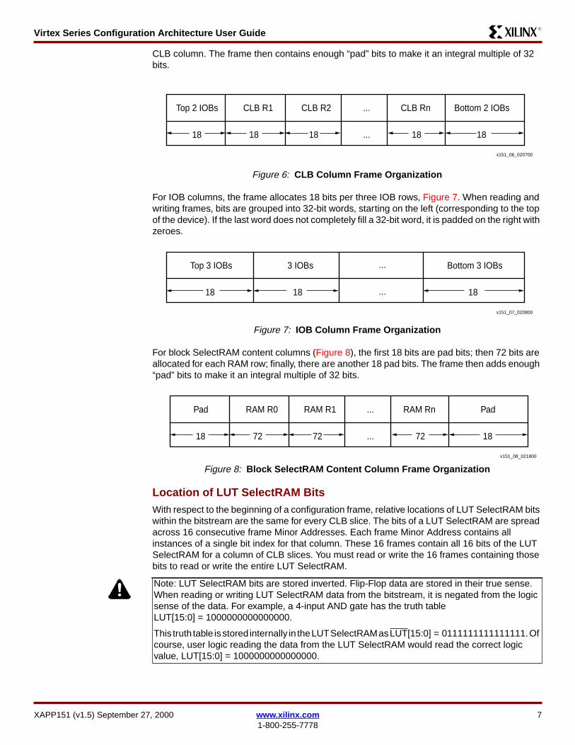
Virtex Series Configuration Architecture User GuideR13
CLB column The frame then contains enough ldquopadrdquo bits to make it an integral multiple of 32bits
For IOB columns the frame allocates 18 bits per three IOB rows Figure 7 When reading andwriting frames bits are grouped into 32-bit words starting on the left (corresponding to the topof the device) If the last word does not completely fill a 32-bit word it is padded on the right withzeroes
For block SelectRAM content columns (Figure 8) the first 18 bits are pad bits then 72 bits areallocated for each RAM row finally there are another 18 pad bits The frame then adds enoughldquopadrdquo bits to make it an integral multiple of 32 bits
Location of LUT SelectRAM BitsWith respect to the beginning of a configuration frame relative locations of LUT SelectRAM bitswithin the bitstream are the same for every CLB slice The bits of a LUT SelectRAM are spreadacross 16 consecutive frame Minor Addresses Each frame Minor Address contains allinstances of a single bit index for that column These 16 frames contain all 16 bits of the LUTSelectRAM for a column of CLB slices You must read or write the 16 frames containing thosebits to read or write the entire LUT SelectRAM
Figure 6 CLB Column Frame Organization
Figure 7 IOB Column Frame Organization
Figure 8 Block SelectRAM Content Column Frame Organization
Note LUT SelectRAM bits are stored inverted Flip-Flop data are stored in their true senseWhen reading or writing LUT SelectRAM data from the bitstream it is negated from the logicsense of the data For example a 4-input AND gate has the truth tableLUT[150] = 1000000000000000
This truth table isstored internally in theLUTSelectRAMasLUT[150] = 0111111111111111Ofcourse user logic reading the data from the LUT SelectRAM would read the correct logicvalue LUT[150] = 1000000000000000
Top 2 IOBs13 Bottom 2 IOBs1313
CLB Rn1313
13 18131813181318131813
CLB R213CLB R113
x151_06_020700
Top 3 IOBs Bottom 3 IOBs1313
181818
3 IOBs
x151_07_020800
Pad PadRAM Rn
1872727218
RAM R1RAM R0
x151_08_021800
XAPP151 (v15) September 27 2000 wwwxilinxcom 71-800-255-7778
Virtex Series Configuration Architecture User GuideR13
ConfigurationData Operations
Reading Configuration DataConfiguration information can be read from the Virtex devices if readback is enabled in thecurrent configuration (See the description of the Control Register field SBITS on page 21)CLB and IOB configuration data can be read while the device is operating
When reading data from a Virtex device a pad frame is read before any of the data framesThis is in addition to the pad word in each data frame The pad frame must be included in theword count to be read from the device
Each frame read from the device consists of the number of words shown in Table 3
For example the XCV150 has 16-word frames When reading frames the first word of a frameis a pad word Including the pad frame the XCV150 has 1899 (3038416) frames (SeeFigure 9)
Writing Configuration DataConfiguration information can be written to a Virtex device while the device is running if writingis enabled in the current configuration (See the Control Register field SBITS in Table 23) Re-writing the same configuration data does not generate any transient signals
Changing configuration data may generate transient signals especially if LUT values or signalrouting is changed For this case all the logic cells and routing can be placed in a non-contentious state by asserting the GHIGH_B signal See the description for the CommandRegister (CMD) on page 18
When writing configuration data to the Virtex device whether from the SelectMAP or JTAGinterfaces the data frames are written to the device with each frame followed by a pad wordAfter all the data frames are written a pad frame must be written (to flush internal pipelines)The pad words and pad frame must be included in the number of words to be written to thedevice (Table 3)
For example the XCV1000 has 39-word frames When writing frames the last word of theframe is a pad word Including the pad frame the XCV1000 has 4779 (18638139) framesSee Figure 10)
Altering Configuration DataVirtex devices support the Read-Modify-Write (RMW) method of changing LUT SelectRAMdata Therefore it is possible to read or alter the contents of one or more LUT SelectRAMsthrough the JTAG or SelectMAP interfaces When writing data to one or more LUTSelectRAMs all the bits in the frame must have valid configuration information This can beassured by altering valid configurations from bitstream files or from frames read from a properlyconfigured Virtex device When using the RMW method it may be expeditious to read the dataignoring the pad frame and the pad word of only the first frame This aligns the remaining
Pad Frame (16 words)Pad Word Data Frame 0 (15 words)
hellip
hellip
Pad Word Data Frame n (15 words)
Figure 9 XCV150 Frame Padding for Device Read
Data Frame 0 (38 words) Pad Word
hellip
Data Frame n (38 words) Pad WordPad Frame (39 words)
Figure 10 XCV1000 Frame Padding for Device Write
8 wwwxilinxcom XAPP151 (v15) September 27 20001-800-255-7778
Virtex Series Configuration Architecture User GuideR13
configuration data in the Device Write format After modifying the configuration the altered datacan be written to the Virtex device followed by a pad word and a pad frame
It is not necessary to retain the contents of the pad frame or pad words However pad wordsand pad frames are included in the CRC calculation
Definitions Two sets of variables are defined to determine where a desired bit is in the configuration dataThe first is a set of ldquoindependentrdquo variables or design attributes namely characteristics of thedesign that are known ie the device size and which CLB and bit(s) within the CLB to locateTable 4 The second set is a set of ldquodependentrdquo variables or design variables namely valuesthat must be calculated to find the bit(s) of interest listed in Table 5
Note Frames span an entire column of CLB slices (or IOBs) Thus when changing LUTSelectRAM bit 0 for a single CLB slice (eg R3C4S1) LUT SelectRAM bit 0 for all slices inthat column (ie RC4S1) is written with the same command One must ensure that either allother data in the slice is constant or changed externally through partial configurations
LUT SelectRAMs not configured externally should not lie in the same slice with LUTs or LUTSelectRAMs that are re-configured externally Such a mixture can cause the unrelated LUTSelectRAM data to be re-configured when the frames are written to the device Figure 11shows what can happen if this restriction is not observed
In this example it is the objective to perform a Read-Modify-Write on the LUT SelectRAM inR2C3S1 in column 3 which is shown in the first column in the figure Row 2 contains a LUTcontaining the value AB Row 3 contains a SelectRAM containing the value C3 Because theRead and Write operations operate on an entire frame the RAM in R3C3S1 is also read andwritten when R2C3S1 is read and written Performing the Readback operation reads all theLUT and SelectRAM values for the column Before the new value for the LUT is written it ispossible for the on-chip circuitry to write a new value such as 14 into the SelectRAM Whenthe new value BD is written via the configuration interface into LUT R2C3S1 the value C3 isalso written into RAM R3C3S1 This may not always be desirable (It is design-dependent)
Figure 11 Potential Write Conflicts
x151_11_020800
LUT R2C3S113AB13
RAM R3C3S113C313
Before13Readback
13
LUT R2C3S113AB13
RAM R3C3S1131413
Before13Configuration 13
Write
13
LUT R2C3S113BD13
RAM R3C3S113C313
After13Configuration13
Write
13
Table 4 Design Attributes (Independent Variables)
Term Definition
Chip_Cols of CLB columns on the Virtex device
Chip_Rows of CLB rows on the Virtex device
Chip_Rams of block SelectRAM columns on the Virtex device
RAM_Space Spacing of block SelectRAM columns (in terms of CLB columns)
FL of 32-bit words in the frame
XAPP151 (v15) September 27 2000 wwwxilinxcom 91-800-255-7778
Virtex Series Configuration Architecture User GuideR13
RW 1 for Read 0 for Write
CLB_Col Column number of the desired CLB
CLB_Row Row number of the desired CLB
Slice 0 or 1
FG 0 for the F-LUT 1 for the G-LUT
lut_bit The desired bit from the given LUT Bits in the LUT are indexed from 0 to 15
XY 0 for the X Flip-Flop 1 for the Y Flip-Flop
RAM_Col Column number of the desired block SelectRAM
RAM_Row Row number of the desired block SelectRAM
ram_bit The desired bit from the given block SelectRAM Bits are indexed from 0 to4095
Table 5 Design Variables (Dependent Variables)
Term Definition
MJA Frame Major Address
MNA Frame Minor Address
fm_st_wd The index of the word within a full configuration segment that correspondsto the starting word of the desired frame A full configuration segment isdefined as the following 1) for CLBIOB all CLB IOB and RAMinterconnect frames beginning at MJA=0 MNA=0 and 2) for blockSelectRAM all RAM content frames for the given RAM column Words arenumbered starting at 0
fm_wd The index of the 32-bit word within a frame that contains the desired bitWords in a frame are numbered starting at 0
fm_wd_bit_idx The bit index of the desired bit within frame word fm_wd Words areindexed in ldquobig-endianrdquo style with bit 31 on the left and bit 0 on the right
fm_bit_idx Bit index within a frame of the desired bit Numbered starting with 0 as theleft-most (first) bit Bit numbering within a frame continues across all thewords in the frame
Table 6 Functions used in Equations
Functions Definition
floor(x) The largest integer not larger than x Eg floor(31) = 3 because the nextlargest integer 4 is larger than 31 floor(3)=3
ceiling(x) The smallest integer greater than or equal to x For example ceiling(32) = 4because 4 is greater than 32 and 3 is not ceiling (4) = 4
The modulus operation 5 2 = 1 5 3 = 2 5 5 = 0
Table 4 Design Attributes (Independent Variables) (Continued)
Term Definition
10 wwwxilinxcom XAPP151 (v15) September 27 20001-800-255-7778
Virtex Series Configuration Architecture User GuideR13
CLB LUTSelectRAMDependentVariables
Table 7 shows equations for the LUT SelectRAM ldquoDependent Variablesrdquo that were defined inTable 5
Virtex-E CLB LUT SelectRAM Dependent VariablesThe additional block SelectRAM columns in Virtex-E devices require an adjustment to the MJAThe following equations calculate the adjustment necessary for each of the affected dependentvariables For each variable calculate the base value based upon the Virtex equations onlyand then add the resulting Virtex adjustment
The left and right sides of the device are treated differently
LUT SelectRAM ExamplesSee ldquoExamplesrdquo on page 27 for several examples of reading and evaluating configuration dataThe examples illustrate how to make use of these equations to find the desired data in abitstream
Table 7 Virtex Equations for LUT SelectRAM Dependent Variables
Term Definition
MJA if (CLB_Col le Chip_Cols2)then Chip_Cols ndash CLB_Col times 2 + 2else 2 times CLB_Col ndash Chip_Cols ndash 1
MNA lut_bit + 32 ndash Slice times (2 times lut_bit + 17)
fm_bit_idx 3 + 18 times CLB_Row ndash FG + RW times 32
fm_st_wd FL times (8 + (MJA ndash1) times 48 + MNA) + RW times FL
fm_wd floor(fm_bit_idx32)
fm_wd_bit_idx 31 + 32 times fm_wd ndash fm_bit_idx
Notes
bull Do NOT input the final results back into the original Virtex equations (eg do not useMJAfinal value to calculate fm_st_wd)
bull MJAfinal = MJA + MJA_adj
bull fm_st_wdfinal = fm_st_wd + fm_st_wd_adj
Table 8 CLB Location
CLB Location CLB Column
Left CLB_Col le Chip_Cols2
Right CLB_Col gt Chip_Cols2
Table 9 Virtex-E Families Adjustments for LUT SelectRAM Dependent Variables
Term Definition
MJA_adj Left RAM_Bound = (Chip_Rams2 - 1) x RAM_SpaceMJA_adj = 2 x ceiling((RAM_Bound - CLB_Col + 1) RAM_Space)
Right
RAM_Bound = Chip_Cols - (Chip_Rams2 - 1) x RAM_Space + 1MJA_adj = 2 x ceiling((CLB_Col - RAM_Bound + 1) RAM_Space)
fm_st_wd_adj FL times (27 x MJA_adj)
XAPP151 (v15) September 27 2000 wwwxilinxcom 111-800-255-7778
Virtex Series Configuration Architecture User GuideR13
CLB Flip-FlopDependentVariables
Equations for the CLB flip-flops can be found in Table 10 Their locations are calculatedsimilarly to the LUT SelectRAM locations Equations for the CLB FF Dependent Variables aredefined in Table 5
Virtex-E CLB Flip-Flop Dependent VariablesApply the adjustments given in Table 8 and Table 9
IOB DependentVariables
Each IOB contains four values that can be captured into special registers These values are
bull I mdash the input flip-flop
bull O mdash the output flip-flop
bull T mdash the flip-flop for the tri-state control
bull P mdash the value of the IO pad
These values are captured by utilizing the CAPTURE_VIRTEX symbol in your design TheLibraries Guide has more details on the use of this symbol The following registers will be readas part of the readback data
Access to the IOB flip-flops is different for the top and bottom IOBs versus the left and rightIOBs
The top and bottom IOBs are part of the CLB column frames There are two IOBs at the top andbottom of each CLB column
The left and right IOBs are in columns by themselves There are three IOBs per CLB row
IOBs are numbered clockwise around the die Pad 1 is located at the left side of the top edgeabove CLB column 1 The equations for where to find IOB flip-flops in the bitstream are basedon the pad number which is the same for a given size device not the package pin name whichvaries from package to package The mapping from package pin names to pad numbers canbe found in EPIC or fpga_editor
Table 11 contains the numeric pad indices for the pads on all four edges of the device in termsof the number of CLB columns and rows on the device
Table 10 Virtex Equations for CLB FF Dependent Variables
Term Definition
MJA if (CLB_Col le Chip_Cols2)then Chip_Cols ndash CLB_Col times 2 + 2else 2 times CLB_Col ndash Chip_Cols ndash 1
MNA Slice times (12 times XY ndash 43) ndash 6 times XY + 45
fm_bit_idx (18 times CLB_Row) + 1 + (32 times RW)
fm_st_wd FL times (8 + (MJA ndash1) times 48 + MNA) + RW times FL
fm_wd floor(fm_bit_idx32)
fm_wd_bit_idx 31 + 32 times fm_wd ndash fm_bit_idx
12 wwwxilinxcom XAPP151 (v15) September 27 20001-800-255-7778
Virtex Series Configuration Architecture User GuideR13
Table 12 shows the equations for the dependent variables for the IOB flip-flops The variable iin this table refers to the index of pad i
Table 11 IOB Pad Indices
PadLocation Pad Index i
Top 1 le i le Chip_Cols times 2
Right Chip_Cols times 2 +1 le i le Chip_Cols times 2 + Chip_Rows times 3
Bottom Chip_Cols times 2 + Chip_Rows times 3 + 1 le i le Chip_Cols times 4 + Chip_Rows times 3
Left Chip_Cols times 4 + Chip_Rows times 3 + 1 le i le Chip_Cols times 4 + Chip_Rows times 6
Table 12 Equations for IOB Dependent Variables
Term Definition
MJA
Topif (i le Chip_Cols)then Chip_Cols ndash ceiling(i2) times 2 + 2else 2 times ceiling (i2) ndash Chip_Cols ndash1
Right Chip_Cols + 1
Bottomif (i gt 3 times (Chip_Cols + Chip_Rows))then 2 times ceiling((i ndash 3 times Chip_Cols ndash 3 times Chip_Rows)2)else Chip_Cols ndash 2 times floor((i ndash 2 times Chip_Cols ndash 3 times Chip_Rows ndash 1)2) ndash 1
Left Chip_Cols + 2
MNA
Top
I ndash 25 times (i2) + 45
O ndash 13 times (i2) + 39
T ndash 5 times (i2) + 35
P ndash 4 times (i2) + 25
Right
I t = (i ndash 2 times Chip_Cols) 3 MNA = 275 times t2 ndash 575 times t + 32
O t = (i ndash 2 times Chip_Cols) 3 MNA = 215 times t2 ndash 515 times t + 38
T t = (i ndash 2 times Chip_Cols) 3 MNA = 175 times t2 ndash 475 times t + 42
P 50
Bottom
I 25 times ((i ndash 2 x Chip_Cols - 3 x Chip_Rows)2) + 20
O 13 times ((i ndash 2 x Chip_Cols - 3 x Chip_Rows)2) + 26
T 5 times ((i ndash 2 x Chip_Cols - 3 x Chip_Rows)2) + 30
P 4 times ((i ndash 2 x Chip_Cols - 3 x Chip_Rows)2) + 21
Left
I t = (i ndash 4 x Chip_Cols - 3 x Chip_Rows)3 MNA = 175 times t2 ndash 475 times t + 45
O t = (i ndash 4 x Chip_Cols - 3 x Chip_Rows)3 MNA = 235 times t2 ndash 535 times t + 39
T t = (i ndash 4 x Chip_Cols - 3 x Chip_Rows)3 MNA = 275 times t2 ndash 575 times t + 35
P 50
XAPP151 (v15) September 27 2000 wwwxilinxcom 131-800-255-7778
Virtex Series Configuration Architecture User GuideR13
Virtex-E IOB Dependent VariablesSimilar to CLB dependent variables only the variables affected by the major address aredifferent in Virtex-E and Virtex-EM devices versus Virtex devices A simple way to account forthe change is to determine the CLB column where the pad resides (only true for top andbottom) Then the adjustment calculated for the CLB column can be applied The conversionto CLB columns is found in Table 13
fm_bit_idx
Top 32 times RW
Right
I O ampT 18 times (1 + floor ((i ndash 2 times Chip_Cols ndash 1)3)) + 32 times RW
Pt = (i ndash 2 times Chip_Cols) 3fm_bit_idx = 18 times (1 + floor ((i ndash 2 times Chip_Cols ndash 1)3)) + 6 times t2 ndash 17 times t + 15 + 32 timesRW
Bottom 18 times (Chip_Rows + 1)+ 32 times RW
Left
I O ampT18 times (Chip_Rows ndash floor((i ndash 4 times Chip_Cols ndash 3 times Chip_Rows ndash 1)3)) + 32 times RW
Pt = (i ndash 4 times Chip_Cols ndash 3 times Chip_Rows)3fm_bit_idx = 18 times (Chip_Rows ndash floor ((i ndash 4 times Chip_Cols ndash 3 times Chip_Rows ndash 1)3))ndash 105 times t2 + 215 times t + 4 + 32 times RW
fm_st_wdif (MJA gt Chip_Cols + 1)then FL times (54 times MJA ndash 46 + MNA ndash 6 times Chip_Cols) + RW times FLelse FL times (8 + (MJA ndash1) times 48 + MNA) + RW times FL
fm_wd floor (fm_bit_idx32)
fm_wd_bit_idx 31 + 32 times fm_wd ndash fm_bit_idx
Table 12 Equations for IOB Dependent Variables (Continued)
Term Definition
Table 13 Pad -gt CLB Column
Term Definition
CLB_ColTop ceiling(i2)
Bottom ceiling((4 x Chip_Cols + 3 x Chip_Rows + 1 - i)2)
Table 14 Virtex-E Families Adjustments for IOB Dependent Variables
Term Definition
MJA_adj
Top use Table 8 and Table 9
Right Chip_Rams
Bottom use Table 8 and Table 9
Left Chip_Rams
fm_st_wd_adj FL times (27 x MJA_adj)
14 wwwxilinxcom XAPP151 (v15) September 27 20001-800-255-7778
Virtex Series Configuration Architecture User GuideR13
BlockSelectRAMDependentVariables
The equations for the block SelectRAM dependent variables are given in Table 15 Therelationship of a particular memory cell index in the context of a given configuration is describedin XAPP130 ldquoUsing the Vir tex Bloc k SelectRAM+ Resour cerdquo
Virtex-E Block SelectRAM Dependent VariablesThe RAM major address numbering scheme changed slightly such that the lowest MJA on theleft side is now 2 instead of 0 As in the case for the CLB equations the adjustments belowshould be applied after the Virtex equations
Table 15 Virtex Equations for Block SelectRAM Dependent Variables
Term Definition
MJAif (RAM_Col lt Chip_Rams2)then 2 x (Chip_Rams2 - 1 - RAM_Col)else 2 x (RAM_Col - Chip_Rams2) + 1
MNA
1 x floor(((ram_bit 64) 64)32) + 2 x floor(((ram_bit 64) 32)16)+ 4 x floor(((ram_bit 64) 16)8) + 8 x floor(((ram_bit 64) 8)4)+ 16 x floor(((ram_bit 64) 4)2) + 32 x floor(((ram_bit 64) 2)1)equivalent to MNA = div64[05] where div64[50] = floor(ram_bit64)
fm_bit_idxobtain value for bitpos from Table 16
fm_bit_idx = 18 + 72 x RAM_Row + bitpos
fm_st_wd FL times MNA + RW times FL
fm_wd floor(fm_bit_idx32)
fm_wd_bit_idx 31 + 32 times fm_wd ndash fm_bit_idx
Table 16 Virtex Block SelectRAM Bit Position Within a Given Block SelectRAM
ram
_bit
6
4
bitp
os
ram
_bit
6
4
bitp
os
ram
_bit
6
4
bitp
os
ram
_bit
6
4
bitp
os
ram
_bit
6
4
bitp
os
ram
_bit
6
4
bitp
os
ram
_bit
6
4
bitp
os
ram
_bit
6
4
bitp
os
0 42 8 45 16 29 24 26 32 43 40 44 48 28 56 27
1 58 9 61 17 13 25 10 33 59 41 60 49 12 57 11
2 41 10 46 18 30 26 25 34 40 42 47 50 31 58 24
3 57 11 62 19 14 27 9 35 56 43 63 51 15 59 8
4 50 12 53 20 21 28 18 36 51 44 52 52 20 60 19
5 49 13 54 21 22 29 17 37 48 45 55 53 23 61 16
6 66 14 69 22 5 30 2 38 67 46 68 54 4 62 3
7 65 15 70 23 6 31 1 39 64 47 71 55 7 63 0
Table 17 Virtex-E and Virtex-EM Adjustments for Block SelectRAM DependentVariables
Term Definition
MJA_adj if (RAM_Col lt Chip_Rams2) MJA_adj = 2
XAPP151 (v15) September 27 2000 wwwxilinxcom 151-800-255-7778
Virtex Series Configuration Architecture User GuideR13
ConfigurationLogic Basics
Configuration DataConfiguration data is organized as 32-bit words There are two major commands that theconfiguration data can contain Read and Write A configuration command is executed whenthe configuration command is read or written to the appropriate command register
The OP field contains 01 for a Read operation and 10 for a Write operation (See Figure 12)
A command is organized as a packet with a header word and optional data words The headerword is the first word written to the appropriate command register for a read or write operationThe header word contains a type field (001) an operand field a register address field and aword count field The format for the command header is shown in Figure 13 on page 17
The Register Address field defines the target of this command as defined in Table 18 on page17
The header word count field contains an integer between 0 and 2047 and indicates thenumber of words that follow the header Larger word counts (between 2048 and 1048575words) are achieved by setting the header word count to 0 The Extension header word has atype field = 010 an OP field that must match the OP field in the preceding Command Headerword and a 20-bit word count this format is shown Figure 14 on page 17
Configuration FlowVirtex devices are configured by presenting configuration data to the SelectMAP or JTAGinterfaces in a specific sequence
For Initial Configuration
1 Issue one or more pad words (SelectMAP only)
2 Issue Sync word (SelectMAP only)
3 Reset CRC
4 Set FLR
5 Set COR
6 Set MASK
7 Set CTL (Set PERSIST if you want to keep SelectMAP active after this configuration)
8 Issue a SWITCH (switch CCLK frequency) command to the CMD register This isnecessary only in Master Serial configuration mode
Reading Configuration
These commands can be issued to read a full configuration or for a partial configuration afterthe device has been completely configured
1 Issue a Sync word (SelectMAP only) if the previous configuration command was aborted
2 Set the FAR to the starting address
3 Issue a RCFG (read configuration) command to the CMD register
4 Write the number of words to be read to the FDRO register
5 Flush the command pipeline with a pad word
6 Read data frames
OP CODERead 01Write 10
Figure 12 OP Field Code
16 wwwxilinxcom XAPP151 (v15) September 27 20001-800-255-7778
Virtex Series Configuration Architecture User GuideR13
Writing Configuration
These commands can be issued either as part of an initial configuration or for a partialconfiguration after the device has been configured
1 Issue a Sync word (SelectMAP only) if the previous configuration command was aborted
2 If the frames being written can cause contention then assert the GHIGH_B signal
3 Set the FAR to the starting address
4 Issue a WCFG (write configuration) command to the CMD register
5 Write the number of words to be written to the FDRI register
6 Write data frames
7 If the GHIGH_B signal was asserted de-assert it by writing the LFRM (Last Frame)command to the CMD register and write one pad frame
ConfigurationRegisters
Configuration logic is accessed and controlled via a collection of 32-bit registers called theconfiguration registers (see Table 18) Registers are described in the following sections
Type OP Register Address RSV Word Count31 30 29 28 27 26 25 24 23 22 21 20 19 18 17 16 15 14 13 12 11 10 9 8 7 6 5 4 3 2 1 00 0 1 x x 0 0 0 0 0 0 0 0 0 0 x x x x 0 0 x x x x x x x x x x x
Notes1 Locations within fields containing a zero or one must have these values An X in a bit field indicates that the value is variable and must
be set2 Heavy vertical lines are used to separate fields Light vertical lines separate nibbles in the word
Figure 13 Command Header Format
Type OP Word Count31 30 29 28 27 26 25 24 23 22 21 20 19 18 17 16 15 14 13 12 11 10 9 8 7 6 5 4 3 2 1 00 1 0 x x 0 0 0 0 0 0 0 x x x x x x x x x x x x x x x x x x x x
Notes1 Locations within fields containing a zero or one must have these values An X in a bit field indicates that the value is variable and must
be set2 Heavy vertical lines are used to separate fields Light vertical lines separate nibbles in the word
Figure 14 Large Block Count Header Extension Format
Table 18 Configuration Register Addresses
Register Name Mnemonic RW Binary Address
CRC CRC RW 0000
Frame Address FAR RW 0001
Frame Data Input FDRI W 0010
Frame Data Output FDRO R 0011
Command CMD RW 0100
Control CTL RW 0101
Control Mask MASK RW 0110
Status STAT R 0111
Legacy Output LOUT W 1000
XAPP151 (v15) September 27 2000 wwwxilinxcom 171-800-255-7778
Virtex Series Configuration Architecture User GuideR13
Command Register (CMD)The content of the Command Register (CMD) is interpreted by the configuration state machineConfiguration commands control the operation of the configuration state machine the FrameData Register (FDR) and some of the global signals The command in the Command Registeris executed each time the FAR is loaded with a new value The effect of each command isdefined in Table 19
Configuration Option COR RW 1001
Reserved mdash mdash 1010
Frame Length FLR RW 1011
Reserved mdash mdash 1100
Reserved mdash mdash 1101
Reserved mdash mdash 1110
Reserved mdash mdash 1111
Table 18 Configuration Register Addresses (Continued)
Register Name Mnemonic RW Binary Address
Table 19 Configuration Commands
Cmd Code Description
Rsvd 0000 Reserved
WCFG 0001Write Configuration Data mdash Used prior to writing configuration data to the FDRI It takes theinternal configuration state machine through a sequence of states that control the shifting of the FDRand the writing of the configuration memory (See Frame Data Input Register (FDRI) on page 24)
Rsvd 0010 Reserved
LFRM 0011Last Frame mdash This command is loaded prior to writing the last (pad) data frame if the GHIGH_Bsignal was asserted This command is not necessary if the GHIGH_B signal was not asserted Thisallows overlap of the last frame write with the release of the GHIGH_B signal
RCFG 0100Read Configuration Data mdash Used prior to reading frame data from the FDRO Similar to the WCFGcommand in its effect on the FDR (see Frame Data Output Register (FDRO) on page 24)
START 0101Begin Startup Sequence mdash Starts the startup sequence This command is also used to start ashutdown sequence prior to partial re-configuration The Startup Sequence begins with the nextsuccessful CRC check (see Cyclic Redundancy Check (CRC) on page 22)
RCAP 0110Reset Capture mdash Used when performing capture in single-shot mode This command must be usedto reset the capture signal if single-shot capture has been selected
RCRC 0111 Reset CRC mdash Used to reset CRC register (see Cyclic Redundancy Check (CRC) on page 22)
AGHIGH 1000Assert GHIGH_B Signal mdash Used prior to re-configuration to prevent contention while writing newconfiguration data All CLB outputs and signals are forced to a one
SWITCH 1001Switch CCLK Frequency mdash Used to change (increase) the frequency of the Master CCLK Thenew frequency is specified in Table 21
Rsvd 1010 Reserved
Rsvd 1011 Reserved
Rsvd 1100 Reserved
18 wwwxilinxcom XAPP151 (v15) September 27 20001-800-255-7778
Virtex Series Configuration Architecture User GuideR13
Configuration Option Register (COR)The Configuration Option Register (COR) is used to select configuration options that areillustrated in Figure 15 and defined in Table 20 Entries in this table are further explained in thefollowing tables
Rsvd 1101 Reserved
Rsvd 1110 Reserved
Rsvd 1111 Reserved
Table 19 Configuration Commands (Continued)
Cmd Code Description
DO
NE
_PIP
E
DR
IVE
_DO
NE
SIN
GLE
OS
CF
SE
L
SS
CLK
SR
C
LOC
K_W
AIT
SH
UT
DO
WN
DO
NE
_CY
CLE
LCK
_CY
CLE
GT
S_C
YC
LE
GW
E_C
YC
LE
GS
R_C
YC
LE
31 30 29 28 27 26 25 24 23 22 21 20 19 18 17 16 15 14 13 12 11 10 9 8 7 6 5 4 3 2 1 00 x x x x x x x x x x x x x x x x x x x x x x x x x x x x x x x
Notes1 Locations within fields containing a zero or one must have these values An X in a bit field indicates that the value is variable and must
be set2 Heavy vertical lines are used to separate fields Light vertical lines separate nibbles in the word
Figure 15 COR (Configuration of Option Register) Fields
XAPP151 (v15) September 27 2000 wwwxilinxcom 191-800-255-7778
Virtex Series Configuration Architecture User GuideR13
Table 21 shows the allowed values for the OSCFSEL field of the COR Setting OSCFSEL toone of these values will set the Master CCLK frequency to the specified value
Table 20 Configuration Option Register Fields
Field Bit Indices DescriptionBitgenDefault
DONE_PIPE 30
0 No pipeline stage for DONEIN
1 Add pipeline stage to DONEINFPGA waits on DONE that is delayed by one (1) cycle of the StartupClkrather than the pin itself Use this option when StartupClk is running at highspeeds
0
DRIVE_DONE 290 DONE pin is open drain
1 DONE pin is actively driven high0
SINGLE 28 Readback capture is one-shot 0
OSCFSEL 2722 Select CCLK frequency in Master Serial configuration mode 2
SSCLKSRC 2120
Startup sequence clock source00 Cclk01 UserClk1x JTAGClk
0
LOCK_WAIT 1916
4-bit mask indicating which DLL lock signals to wait for during LCK cycleThe 4 bits (from MSB to LSB) correspond to DLLs TL=3 TR=2 BL=1BR=0 (top-left top-right etc) In Virtex-E devices where there are 8 DLLseach mask bit applies to the 2 DLLs in that quadrant of the device Thedefault is not to wait for any DLL lock signals
0
SHUTDOWN 15
Indicate whether doing a startup or shutdown sequence
0 Startup
1 Shutdown sequence
0
DONE_CYCLE 1412 Startup phase in which DONE pin is released 3
LCK_CYCLE 119 Stall in this startup phase until DLL locks are asserted 7
GTS_CYCLE 86 Startup phase in which IOs switch from tri-state to user design 4
GWE_CYCLE 53 Startup phase in which the global write-enable is asserted 5
GSR_CYCLE 20 Startup phase in which the global setreset is negated 5
Table 21 OSCFSEL-Specified Master CCLK Frequencies)
CCLK(MHz) OSCFSEL
CCLK(MHz) OSCFSEL
CCLK(MHz) OSCFSEL
43 000010 13 001010 41 100111
54 010001 15 001101 45 110011
69 000100 20 010111 51 101010
81 000101 26 011010 55 110100
20 wwwxilinxcom XAPP151 (v15) September 27 20001-800-255-7778
Virtex Series Configuration Architecture User GuideR13
Table 22 shows the values of the DONE_CYCLE LCK_CYCLE GTS_CYCLE GWE_CYCLEand GSR_CYCLE fields in COR This table shows the step in the start-up sequence when eachof these signals becomes active
Control Register (CTL)The Control Register (CTL) fields are illustrated in Figure 16 on page 21 and defined inTable 23
92 000110 30 011101 60 101101
100 000111 34 110010 mdash mdash
Notes1 These values are accurate to +45 ndash 30
Table 22 COR Startup Cycle Fields
FieldValue
DONE_CYCLE(DONE Active)
GTS_CYCLE(GTS_CFGInactive)
GSR_CYCLE(GSR Inactive)
GWE_CYCLE(GWE Active) LCK_CYCLE
000 1 1 1 1 0
001 2 2 2 2 1
010 3 3 3 3 2
011 4 (default) 4 4 4 3
100 5 5 (default) 5 5 4
101 6 6 6 (default) 6 (default) 5
110 mdash DoneIndagger DoneIndagger DoneIndagger 6
111 Keep State Keep State Keep State Keep State Donrsquot Wait(default)
Notes1 dagger DONE if DonePipe = No else the delayed version of DONE
Table 21 OSCFSEL-Specified Master CCLK Frequencies) (Continued)
CCLK(MHz) OSCFSEL
CCLK(MHz) OSCFSEL
CCLK(MHz) OSCFSEL
SB
ITS
PE
RS
IST
GT
S_U
SR
_B
31 30 29 28 27 26 25 24 23 22 21 20 19 18 17 16 15 14 13 12 11 10 9 8 7 6 5 4 3 2 1 00 0 0 0 0 0 0 0 0 0 0 0 0 0 0 0 0 0 0 0 0 0 0 x x x 0 0 0 0 0 x
Notes1 Locations within fields containing a zero or one must have these values An X in a bit field indicates that the value is variable and must
be set2 Heavy vertical lines are used to separate fields Light vertical lines separate nibbles in the word
Figure 16 Control Register Fields
XAPP151 (v15) September 27 2000 wwwxilinxcom 211-800-255-7778
Virtex Series Configuration Architecture User GuideR13
Cyclic Redundancy Check (CRC)A data input error checking mechanism is provided through the Cyclic Redundancy Check(CRC) register When data is written to any configuration register (except LOUT) a 16-bit CRCvalue is calculated using both the register data and the address This value is saved in the CRCregister At the end of any series of writes a pre-calculated CRC block-check value may bewritten to the CRC register If the resulting value is non-zero an error is indicated TheCRC_ERROR bit is accessible through the status register If a CRC error is detectedconfiguration logic is put in the ERROR mode The following section is an algorithm forcomputing CRC
CRC Algorithm Initialization bcc = 0skip_pad = truemore_words = true Check for write operation do
w = next_wordif (w[3127] == rsquo00101rsquo)
A Read OP Donrsquot use in CRCwc = w[100]if (wc == 0)
w = next_wordwc = w[190]
while (wc-- gt 0)
w = next_word
elsif (w[3127] == rsquo00110rsquo)
A Write OP Use in CRC addr = w[1613]if (addr Π0124569DB)
wc = w[100]if (wc == 0)
wc is in next word w = next_wordwc = w[190]
while (wc-- gt 0)
w = next_wordsw[350] = addr wordfor (i=0 ilt36 i++)
Table 23 Control Register Bits
NameBit
Indices Description
SBITS 87 Security level0 ReadWrite OK (default)1 Readback disabled23 Readback disabled Writing disabled except CRCregister
PERSIST 6 Configuration interface remains after configuration0 No (default)1 Yes
GTS_USR_B 0 Active-low global tristate IOs Turn off pull-ups ifGTS_CFG_B is also asserted
22 wwwxilinxcom XAPP151 (v15) September 27 20001-800-255-7778
Virtex Series Configuration Architecture User GuideR13
x16 = bcc[15] XOR sw[i]x15 = bcc[14] XOR x16x2 = bcc[1] XOR x16bcc[150] =
x15bcc[132]x2bcc[0]x16 Note the bit order crc[150] = bcc[015]
else
Pad word - ignore
while (more_words)
Frame Address Register (FAR)The Frame Address Register (FAR) holds the address of the current frame The address isdivided into three parts the block type the major address and the minor address The blocktype field indicates whether the CLB or block RAM address space is used The command in thecommand register is executed each time the FAR is loaded with a new value
The major address selects the CLB or RAM column the minor address selects the frame withinthe column The minor address is incremented each time a full data frame is read from orwritten to the frame data register If the last frame within the CLB column is selected when theincrement occurs the major address is incremented and the minor address is reset to zerootherwise the minor address is incremented However the block RAM major address is notincremented automatically
See Figure 18 for the definitions of valid values for the block type field The FAR field definitionsare shown in Figure 19
Figure 17 CRC Calculation Register
Note the Block RAM Major Address is not incremented automatically To address a differentBlock RAM Content column the FAR must be loaded with the new Major Address
Type CodesCLB 00RAM 01
Figure 18 Block Type Codes
x151_17_021100
15141312111098765432
1013
01234526272829303101
Address 32-bit Data Word
CRC Calculation Register
CRC Data Input Register
CRC Register [310]
DATA_IN
SHIFT
23
16-bit CRC13150
0000 0000 0000 0000133116
1313
XAPP151 (v15) September 27 2000 wwwxilinxcom 231-800-255-7778
Virtex Series Configuration Architecture User GuideR13
Frame Data Input Register (FDRI)The Frame Data Input Register (FDRI) is used to load configuration frame data into a Virtexdevice
The Frame Data Register (FDR) is a shift register into which data is loaded prior to transfer tothe configuration memory Configuration data is written to the Virtex device by loading thecommand register with the WCFG command and then loading the FDR with at least two framesof 32-bit words
The write operation is pipelined such that the first frame of data is written to the configurationmemory while the second frame is being shifted in The last frame (the pad frame) is alwaysdummy data which is not actually written to the configuration memory Each frame write mustinclude enough 32 bit data words to load the frame fully There is one pad word at the end ofeach frame which is required for the pipelining hardware
Frame Data Output Register (FDRO)The Frame Data Output Register (FDRO) is for reading configuration data or captured datafrom the Virtex device a process called readback Readback is performed by loading thecommand register with the RCFG command and then addressing the FDRO with a readcommand
Frame Length Register (FLR)Near the beginning of the configuration bitstream the Frame Length Register (FLR) is writtenwith the length of a frame as measured in 32-bit words This length count is used to providesequencing information for the configuration read and write operations Note that the FLR mustbe written before any FDR operation works It is not necessary to set the FLR more than onceIf the number of bits in a frame is not evenly divisible by 32 the length count of the frame mustbe rounded up to the next highest integer The values for the FLR for all the current Virtexseries devices are given in Table 24
BlockType
Major Address(Column Address)
Minor Address(Frame Address)
31 30 29 28 27 26 25 24 23 22 21 20 19 18 17 16 15 14 13 12 11 10 9 8 7 6 5 4 3 2 1 00 0 0 0 0 x x x x x x x x x x x x x x x x x x 0 0 0 0 0 0 0 0 0
Notes1 Locations within fields containing a zero or one must have these values An X in a bit field indicates that the value is variable and must
be set2 Heavy vertical lines are used to separate fields Light vertical lines separate nibbles in the word
Figure 19 Frame Address Fields (FAR)
Note The FLR contains a value that is one less than the number of words that are read fromor written to a given frame This is because the extra word needed for pipelining is not counted
Table 24 Frame Length Register Value
Device Row times Col Frame Length Words per Frame FLR Value
XCV50E 16 times 24 384 12 11
XCV100E 20 times 30 448 14 13
XCV150 24 times 36 512 16 15
XCV200E 28 times 42 576 18 17
XCV300E 32 times 48 672 21 20
24 wwwxilinxcom XAPP151 (v15) September 27 20001-800-255-7778
Virtex Series Configuration Architecture User GuideR13
Legacy Output Register (LOUT)The Legacy Output Register (LOUT) is used for daisy chaining the configuration bitstream toother Xilinx devices Data written to the LOUT is serialized and appears on the DOUT pin
Mask Register (MASK)The Mask Register (MASK) is a mask register for writes to the CTL register A 1 in bit N of themask allows that bit position to be written in the CTL register The default value of the mask isall 0s
Status Register (STAT)The Status Register (STAT) is loaded with current values of several control or status signalsThe register can be read via the re-configuration block or via JTAG The fields in the Statusregister are illustrated in Figure 20 The values of the signals given in Table 25 on page 26 canbe read from the status register
XCV400E 40 times 60 800 25 24
XCV405E 40 times 60 800 25 24
XCV600E 48 times 72 960 30 29
XCV800 56 times 84 1088 34 33
XCV812E 56 times 84 1088 34 33
XCV1000E 64 times 96 1248 39 38
XCV1600E 72 times 108 1376 43 42
XCV2000E 80 times 120 1536 48 47
XCV2600E 92 times 138 1728 54 53
XCV3200E 104 times 156 1952 61 60
Table 24 Frame Length Register Value (Continued)
Device Row times Col Frame Length Words per Frame FLR Value
DO
NE
INIT
MO
DE
GH
IGH
_B
GS
R_B
GW
E_B
GT
S_C
FG
IN_E
RR
OR
LOC
K
CR
C_E
RR
OR
31 30 29 28 27 26 25 24 23 22 21 20 19 18 17 16 15 14 13 12 11 10 9 8 7 6 5 4 3 2 1 00 0 0 0 0 0 0 0 0 0 0 0 0 0 0 0 0 x x x x x x x x x x x x x x x
Notes1 An X in a bit field indicates that the value is variable2 Heavy vertical lines are used to separate fields Light vertical lines separate nibbles in the word
Figure 20 Status Register Fields
XAPP151 (v15) September 27 2000 wwwxilinxcom 251-800-255-7778
Virtex Series Configuration Architecture User GuideR13
ConfigurationInterface
There are two configuration interfaces to the Virtex devices mdash the bit-serial Boundary Scaninterface and the 8-bit byte-serial SelectMAP interface Conceptually XCV50 configurationdata appears as in Figure 21
Frames and words within frames are written in the same order in both configuration interfacesstarting with Frame 0 word 0 (the left-most in the picture) followed by word 1 etc Bits withineach word are written from left to right (MSB first) in the bit-serial configuration interfaces
Within the SelectMAP interface data is written a byte at a time A sample word is shown inFigure 22 The top row indicates the device pin names The bottom row indicates the bit indiceswithin a configuration word Byte 0 loads first followed by byte 1 et cetera The MSB of eachbyte (ie bits 31 23 15 and 7) is loaded on pin D0 The LSB of each byte (ie bits 24 16 8and 0) is loaded on pin D7
PartialReconfigurationof CLBs
Partial reconfiguration can be performed with and without shutting down the device Ifcontention occurs it is advised to go through a shutdown sequence prior to loadingconfiguration frames When shutting down the DONE pin will go active and pull low If this is notdesireable the DONE pin can be prevented from going low by selecting the DONE_CYCLE toKeep State (111) Similarly to prevent GSR from becoming active and reseting the currentstate the GSR_CYCLE can be set to Keep State When not shutting down changes occurframe by frame but is completely done by the end of the Last Frame packet (see Example 1)
Table 25 Status Register Bits
Name Bit Indices Description
DONE 14 Input from DONE pin
INIT 13 Value of INIT
MODE 1210 Value of M2 M1 M0 mode pins
GHIGH_B 9 0 = GHIGH_B asserted
GSR_B 8 0 = all flip-flops are ResetSet
GWE_B 7 1 = flip-flops and block RAM are write disabled
GTS_CFG 6 0 = IOs are tri-stated
IN_ERROR 5 Legacy input error
LOCK 41 Output from DLL lock signals 1 = DLL is locked
CRC_ERROR 0 Indicates that a CRC error has occurred
Data Frame 0 (11 words) Pad Word
hellip
Data Frame n (11 words) Pad WordPad Frame (12 words)
Figure 21 XCV50 Frame Padding for Reads
Figure 22 SelectMAP Byte and Bit Ordering
x151_22_021100
D0 D1 D2 D3 D4 D5 D6 D7 D0 D1 D2 D3 D4 D5 D6 D7 D0 D1 D2 D3 D4 D5 D6 D7 D0 D1 D2 D3 D4 D5 D6 D7
Byte 0 Byte 1 Byte 2 Byte 313
26 wwwxilinxcom XAPP151 (v15) September 27 20001-800-255-7778
Virtex Series Configuration Architecture User GuideR13
The DONE pin will not change in this case Figure 23 illustrates a typical shutdownreconfiguration in the CLB address space and restart sequence
Examples Several examples of reading and evaluating configuration data are provided to illustrate thefollowing
Figure 23 Typical Shutdown Reconfiguration in the CLB Address Spaceand Restart Sequence
FFFF FFFF Dummy WordAA99 5566 Sync Word Does not realign an already synchronized SelectMap port3001 2001 COR0080 FF2F Shutdown bit set optionally set bit 29 DRIVE_DONE
Alternately COR may be read bit 15 set and written back3000 8001 CMD0000 0005 Start Shutdown3000 8001 CMD0000 0007 Reset CRC0000 00000000 0000 Clock shutdown sequence0000 00000000 00003000 8001 CMD0000 0008 Assert GHIGH3000 8001 CMD0000 0001 Write Configuration3000 2001 FAR0--- ---- Block Type CLB (00) MajorMinor Address3000 4--- FDRI + Word Count if count is lt1024 Otherwise use TypeII Header
Write FRAME DATAIf CLB Frames are not written to non-consecutive addresses repeat FAR word followedby new MajorMinor Address followed by FDRI + Word Count and then Frame Data
3000 0001 Write CRC---- ---- CRC3000 8001 CMD0000 0003 LFRM3000 4--- FDRI + Word Count
Write PAD FRAME
3001 2001 COR0080 3F2D Default COR Options
Alternately COR may be read bit 15 cleared and written back3000 8001 CMD0000 0005 Begin Startup3000 0001 Write CRC---- ---- CRC
0000 00000000 0000 4 Dummy Words0000 00000000 0000
Example 1 Read and Write Semaphores in an XCV100 at CLB R1 C1 Slice 0 on page 28Example 2 Reading the Complete Configuration from an XCV50 on page 33
XAPP151 (v15) September 27 2000 wwwxilinxcom 271-800-255-7778
Virtex Series Configuration Architecture User GuideR13
Example 1 Read and Write Semaphores in an XCV100 at CLB R1 C1Slice 0Semaphores are a useful communication mechanism documented in XAPP 153 ldquoStatus andControl Semaphore Registers using Partial Reconfigurationrdquo Figure 24 shows an abstractionof a microprocessor writing control information to an FPGA and reading status informationOne convention for implementing semaphores in Virtex devices is to use two bits of a 16-bitdual-port RAM as illustrated in Figure 25 This occupies one CLB slice with the F-LUTimplementing the control semaphore and the status semaphore implemented in the G-LUTAddress 15 of the G-LUT is used for on-chip writes to the semaphore and address 14 of the F-LUT is used for on-chip reads Conversely the off-chip microprocessor is reading the G-LUT[15] and writing F-LUT[14]
Example 3 Read the Slice 0 G-LUT from CLB R1 C1 from the Complete Configuration of anXCV50 on page 34Example 4 Read the Slice 1 F-LUT from CLB R19 C16 from an XCV100 on page 36Example 5 Read All Bits in Slice 0 G-LUTs from CLB C2 and XCV50 on page 39Example 6 Read Block SelectRAM index 387 of RAM R2 C0 from an XCV100E on page 41
Figure 24 Semaphore Abstraction
x151_ 23_021400
Status13
Control13
MicroProcessor FPGA13
Semaphores13
28 wwwxilinxcom XAPP151 (v15) September 27 20001-800-255-7778
Virtex Series Configuration Architecture User GuideR13
Using a Semaphore Abstraction dual-port RAM ensures that the LUT SelectRAMs are placedin the CLB in a predictable manner When writing data to one or more LUT SelectRAMs or flip-flops on the device all bits in the frame must have valid configuration information This isassured by altering valid configurations from bitstream files or from frames read from a properlyconfigured Virtex device The latter approach is used in this example
Figure 25 Semaphore ReadWrite Implementation
Frame 47
15
14
47 46
47 46
x151_ 24_021100
Select Map
Frame 46
DING
F
13
D2D3D4 5D6 7D0D1 D D
1
111
0
111
Chip Interface
G F
13
XAPP151 (v15) September 27 2000 wwwxilinxcom 291-800-255-7778
Virtex Series Configuration Architecture User GuideR13
Attributes for this design are summarized in Table 26
From the equations in Table 7 on page 11 the values shown in Table 27 can be calculated
From off-chip for reading the G-LUT[15] bit read one frame (MNA=47) For writing the F-LUT[14] bit we show how to read then write one frame (MNA=46) as opposed to modifyingdata from a bitstream file (both are valid methods) The frames on the XCV100 contain 13 32-bit words and one pad word Remember that fm_st_wd is calculated assuming the entireconfiguration has been read However only the pad frame and then frames 46 and 47 fromMajor Address 30 are being read The desired bit is in Frame 1 word 1 which is word 15
The commands for reading both frames (and the pad frame) are given in Figure 26
Table 26 Design Attributes for Example 1
Attribute
G-LUT [15] F-LUT [14]
Read Read Write
Chip_Rows 20
Chip_Cols 30
FL 14
CLB_Row 1
CLB_Col 1
Slice 0
FG 1 0
lut_bit 15 14
RW 1 1 0
Table 27 Semaphore Example Variables Equations and Values
Variable Equation
Value(s)
G-LUT[15] F-LUT[14]
Read Read Write
MJA 1 le 302 rArr 30 ndash 1 times 2 + 2 30
MNA lut_bit + 32ndash 0 times () 47 46
fm_bit_idx 3 + 18 times 1 ndash FG + RW times 32 52 53 21
fm_st_wd 14 times (8 + (30 ndash 1) times 48+ 4647) +RW times (14 +1)= 14 times (1400 + 4647) + 14 times RW= 19600 + 14 times 4647 + 14 times RW
20272 20258 20244
fm_wd floor (2032) 1 1 0
fm_wd_bit_idx 31 + 32 times 110 ndash 525321 11 10 10
30 wwwxilinxcom XAPP151 (v15) September 27 20001-800-255-7778
Virtex Series Configuration Architecture User GuideR13
The 42 words read are shown in Figure 27 F-LUT[14] is in the second frame (frame=1word=1) at bit 10 The value read is a 1 but because the LUT bits are inverted the logic valueis zero G-LUT[15] is in word one of the third data frame (frame=2 word=1) at bit 11The valueread is a 1 which is a logic zero
InstructionData
Hex 31 30 29 28 27 26 25 24 23 22 21 20 19 18 17 16 15 14 13 12 11 10 9 8 7 6 5 4 3 2 1 0
Sync Word AA99 5566 1 0 1 0 1 0 1 0 1 0 0 1 1 0 0 1 0 1 0 1 0 1 0 1 0 1 1 0 0 1 1 0
Write next (1) word to FAR 3000 2001 0 0 1 1 0 0 0 0 0 0 0 0 0 0 0 0 0 0 1 0 0 0 0 0 0 0 0 0 0 0 0 1
CLB MJA=30 MNA=46 003C 5800 0 0 0 0 0 0 0 0 0 0 1 1 1 1 0 0 0 1 0 1 1 1 0 0 0 0 0 0 0 0 0 0
Write next word to CMD 3000 8001 0 0 1 1 0 0 0 0 0 0 0 0 0 0 0 0 1 0 0 0 0 0 0 0 0 0 0 0 0 0 0 1
Register value for RCFG 0000 0004 0 0 0 0 0 0 0 0 0 0 0 0 0 0 0 0 0 0 0 0 0 0 0 0 0 0 0 0 0 1 0 0
Read from FDRO 2800 602A 0 0 1 0 1 0 0 0 0 0 0 0 0 0 0 0 0 1 1 0 0 0 0 0 0 0 1 0 1 0 1 0
Flush pipe 0000 0000 0 0 0 0 0 0 0 0 0 0 0 0 0 0 0 0 0 0 0 0 0 0 0 0 0 0 0 0 0 0 0 0
(read 42 words)
Notes1 Binary data is grouped in two ways for ease of interpretation Thin vertical lines separate nibble boundaries Heavy vertical lines
separate field boundaries
Figure 26 Commands to Read Two Data Frames
XAPP151 (v15) September 27 2000 wwwxilinxcom 311-800-255-7778
Virtex Series Configuration Architecture User GuideR13
To write to the F-LUT semaphore start with the second data frame (frame=1) that was justread Words 1 - 13 of that frame will become words 0 - 12 of the frame to be written Word 13of this new frame is a pad word and can have any value (typically 0 is chosen) In this newframe set bit 11 of word 0 (zero) to the desired value of the semaphore A pad frame mustfollow the data frame The commands from Figure 28 write these two frames into the device atthe proper location
Frame Word 31 30 29 28 27 26 25 24 23 22 21 20 19 18 17 16 15 14 13 12 11 10 9 8 7 6 5 4 3 2 1 0
0
0 1 1 1 1 1 1 1 1 1 1 1 1 1 1 1 1 1 1 1 1 1 1 1 1 1 1 1 1 1 1 1 1
1 1 1 1 1 1 1 1 1 1 1 1 1 1 1 1 1 1 1 1 1 1 1 1 1 1 1 1 1 1 1 1 1
2 1 1 1 1 1 1 1 1 1 1 1 1 1 1 1 1 1 1 1 1 1 1 1 1 1 1 1 1 1 1 1 1
3 1 1 1 1 1 1 1 1 1 1 1 1 1 1 1 1 1 1 1 1 1 1 1 1 1 1 1 1 1 1 1 1
4 1 1 1 1 1 1 1 1 1 1 1 1 1 1 1 1 1 1 1 1 1 1 1 1 1 1 1 1 1 1 1 1
5 1 1 1 1 1 1 1 1 1 1 1 1 1 1 1 1 1 1 1 1 1 1 1 1 1 1 1 1 1 1 1 1
6 1 1 1 1 1 1 1 1 1 1 1 1 1 1 1 1 1 1 1 1 1 1 1 1 1 1 1 1 1 1 1 1
7 1 1 1 1 1 1 1 1 1 1 1 1 1 1 1 1 1 1 1 1 1 1 1 1 1 1 1 1 1 1 1 1
8 1 1 1 1 1 1 1 1 1 1 1 1 1 1 1 1 1 1 1 1 1 1 1 1 1 1 1 1 1 1 1 1
9 1 1 1 1 1 1 1 1 1 1 1 1 1 1 1 1 1 1 1 1 1 1 1 1 1 1 1 1 1 1 1 1
10 1 1 1 1 1 1 1 1 1 1 1 1 1 1 1 1 1 1 1 1 1 1 1 1 1 1 1 1 1 1 1 1
11 1 1 1 1 1 1 1 1 1 1 1 1 1 1 1 1 1 1 1 1 1 1 1 1 1 1 1 1 1 1 1 1
12 1 1 1 1 1 1 1 1 1 1 1 1 1 1 1 1 1 1 1 1 1 1 1 1 1 1 1 1 1 1 1 1
13 1 1 1 1 1 1 1 1 1 1 1 1 1 1 1 1 1 1 1 1 1 1 1 1 1 1 1 1 1 1 1 1
1
0 0 0 0 0 0 0 0 0 0 0 0 0 0 0 0 0 0 0 0 0 0 0 0 0 0 0 0 0 0 0 0 0
1 1 0 0 0 0 0 0 0 0 0 0 0 1 0 0 0 0 1 1 0 1 1 0 0 0 0 0 0 0 0 0 0 F[14]
2 1 1 1 1 1 0 1 1 0 0 0 0 1 1 1 1 0 0 1 1 1 1 1 0 1 1 0 0 0 0 0 0
3 0 0 0 0 1 1 1 1 1 0 1 1 0 0 0 0 0 0 0 0 0 0 1 1 1 1 1 0 1 1 0 0
4 0 0 0 0 0 0 0 0 1 1 1 1 0 0 0 0 0 0 0 0 0 0 0 0 0 0 1 1 1 1 1 0
5 1 1 0 0 1 1 0 0 0 0 0 0 1 1 0 0 1 0 1 1 0 0 0 0 0 0 0 0 0 0 1 1
6 1 1 1 0 1 1 0 0 0 0 0 0 1 1 1 0 1 1 1 0 1 0 1 1 0 0 0 0 0 0 0 0
7 0 0 1 1 1 1 1 0 1 1 0 0 0 0 1 1 0 0 0 0 1 1 1 1 1 0 1 1 0 0 0 0
8 0 0 0 0 0 0 1 1 1 1 1 0 0 0 0 0 0 0 0 0 0 0 0 0 1 1 1 1 1 0 1 1
9 0 0 0 0 0 0 0 0 0 0 1 1 0 0 0 0 1 1 0 0 0 0 0 0 0 0 0 0 1 1 1 1
10 1 0 1 1 0 0 0 0 0 0 0 0 1 0 1 1 1 1 1 0 1 1 0 0 0 0 0 0 0 0 0 0
11 1 1 1 1 1 0 1 1 0 0 0 0 1 1 1 1 0 0 1 1 1 1 1 0 1 1 0 0 0 0 0 0
12 0 0 0 0 1 1 0 1 1 0 1 1 0 0 0 0 0 0 0 0 0 0 1 1 1 1 1 0 0 0 0 0
13 0 0 0 0 0 0 1 1 0 1 0 1 0 0 0 0 0 0 0 0 0 0 0 0 0 0 0 0 0 0 0 0
2
0 0 0 0 0 0 0 0 0 0 0 0 0 0 0 0 0 0 0 0 0 0 0 0 0 0 0 0 0 0 0 0 0
1 1 0 1 0 0 0 0 0 0 0 0 1 1 0 1 0 1 1 1 0 1 1 0 0 0 0 0 0 0 0 0 0 G[15]
2 1 1 1 1 1 1 1 1 0 0 0 0 1 1 1 1 0 0 1 1 1 1 1 1 1 1 0 0 0 0 0 0
3 0 0 0 0 1 1 1 1 1 1 1 1 0 0 0 0 0 0 0 0 0 0 1 0 1 1 1 1 1 1 0 0
4 0 0 0 0 0 0 0 0 1 1 1 1 0 0 0 0 0 0 0 0 0 0 0 0 0 0 1 1 1 1 1 1
5 1 1 0 0 0 0 0 0 0 0 0 0 1 1 0 0 1 1 1 1 0 0 1 0 0 0 0 0 0 0 1 1
6 1 1 1 1 1 1 0 0 0 0 0 0 1 1 1 1 1 1 1 1 1 1 1 1 0 0 0 0 0 0 0 0
7 0 0 1 1 1 1 1 1 1 1 0 0 0 0 1 1 0 0 0 0 1 1 1 1 1 1 1 1 0 0 0 0
8 0 0 0 0 0 0 1 1 1 1 1 1 0 0 0 0 0 0 0 0 0 0 0 0 1 1 1 1 1 1 1 1
9 0 0 0 0 0 0 0 0 0 0 1 1 0 0 0 0 1 1 0 0 0 0 0 0 0 0 0 0 1 1 1 1
10 1 1 1 1 0 0 0 0 0 0 0 0 1 1 1 1 1 1 1 1 1 1 0 0 0 0 0 0 0 0 0 0
11 1 1 1 1 1 1 1 1 0 0 0 0 1 1 1 1 0 0 1 1 1 1 1 1 1 1 0 0 0 0 0 0
12 0 0 0 0 1 1 0 1 1 1 1 1 0 0 0 0 0 0 0 0 0 0 1 1 1 1 1 0 1 0 0 0
13 0 0 0 0 0 1 1 0 0 1 1 1 0 0 0 0 0 0 0 0 0 0 0 0 0 0 0 0 0 0 0 0
Figure 27 Three Frames Containing the Semaphores
32 wwwxilinxcom XAPP151 (v15) September 27 20001-800-255-7778
Virtex Series Configuration Architecture User GuideR13
Example 2 Reading the Complete Configuration from an XCV50Steps
1 If flip-flop values are needed clock the on-chip signal CAPTURE to capture flip-flopvalues See the Xilinx Libraries Guide for use of the CAPTURE_VIRTEX cell
2 Write the starting frame address (CLB MJA=0 MNA=0) into the FAR
3 Write the RCFG command to the CMD register
4 Address the FDRO register with a READ operation and word count equal to the number of32-bit words in the CLB frames plus one pad frame
5 Read the data following the timing diagrams in the SelectMAP interface section
6 Write the address for RAM block 0 to the FAR
7 Address the FDRO register with a read operation and word count equal to the number of32-bit words in the RAM block plus one pad frame
8 Read the data
9 Write the address for RAM block 1 to the FAR
10 Address the FDRO register with a read operation and word count equal to the number of32-bit words in the RAM block plus one pad frame
11 Read the data
When using SelectMAP mode to read data words from the Virtex device de-assert CS de-assert WRITE assert CS then clock the data out When using JTAG load the JTAG IR
InstructionData
Hex 31 30 29 28 27 26 25 24 23 22 21 20 19 18 17 16 15 14 13 12 11 10 9 8 7 6 5 4 3 2 1 0
Sync Word AA995566
1 0 1 0 1 0 1 0 1 0 0 1 1 0 0 1 0 1 0 1 0 1 0 1 0 1 1 0 0 1 1 0
Write next (1) word to FAR 30002001
0 0 1 1 0 0 0 0 0 0 0 0 0 0 0 0 0 0 1 0 0 0 0 0 0 0 0 0 0 0 0 1
MJA=30 MNA=46 003C5C00
0 0 0 0 0 0 0 0 0 0 1 1 1 1 0 0 0 1 0 1 1 1 0 0 0 0 0 0 0 0 0 0
Write next word to CMD 30008001
0 0 1 1 0 0 0 0 0 0 0 0 0 0 0 0 1 0 0 0 0 0 0 0 0 0 0 0 0 0 0 1
Register value for WCFG 00000001
0 0 0 0 0 0 0 0 0 0 0 0 0 0 0 0 0 0 0 0 0 0 0 0 0 0 0 0 0 0 0 1
Write 28 words to FDRI 3000401C
0 0 1 1 0 0 0 0 0 0 0 0 0 0 0 0 0 1 0 0 0 0 0 0 0 0 0 1 1 1 0 0
Data Word 0 A01AEC00
1 0 1 0 0 0 0 0 0 0 0 1 1 0 1 0 1 1 1 0 1 1 0 0 0 0 0 0 0 0 0 0
Data Word 1 FF0F3FC0
1 1 1 1 1 1 1 1 0 0 0 0 1 1 1 1 0 0 1 1 1 1 1 1 1 1 0 0 0 0 0 0
Data Word 2 0FF002FC
0 0 0 0 1 1 1 1 1 1 1 1 0 0 0 0 0 0 0 0 0 0 1 0 1 1 1 1 1 1 0 0
hellip hellip hellip
Data Word 27 00000000
0 0 0 0 0 0 0 0 0 0 0 0 0 0 0 0 0 0 0 0 0 0 0 0 0 0 0 0 0 0 0 0
Notes1 Binary data is grouped in two ways for ease of interpretation Thin vertical lines separate nibble boundaries Heavy
vertical lines separate field boundaries
Figure 28 Commands to Write a Semaphore Value
XAPP151 (v15) September 27 2000 wwwxilinxcom 331-800-255-7778
Virtex Series Configuration Architecture User GuideR13
(instruction register) with the CFG_OUT instruction Then go to the SDR (Shift-DR) state andshift the data out (See Figure 29)
Example 3 Read the Slice 0 G-LUT from CLB R1 C1 from the CompleteConfiguration of an XCV50The commands for reading the bitstream from the Virtex device are given in Example 1 Readand Write Semaphores in an XCV100 at CLB R1 C1 Slice 0 on page 28 Using an XCV50device the independent attributes are show in Table 28
InstructionData
Hex 31 30 29 28 27 26 25 24 23 22 21 20 19 18 17 16 15 14 13 12 11 10 9 8 7 6 5 4 3 2 1 0
Sync Word AA99 5566 1 0 1 0 1 0 1 0 1 0 0 1 1 0 0 1 0 1 0 1 0 1 0 1 0 1 1 0 0 1 1 0
Write next word to FAR 3000 2001 0 0 1 1 0 0 0 0 0 0 0 0 0 0 0 0 0 0 1 0 0 0 0 0 0 0 0 0 0 0 0 1
CLB MJA=0 MNA=0 0000 0000 0 0 0 0 0 0 0 0 0 0 0 0 0 0 0 0 0 0 0 0 0 0 0 0 0 0 0 0 0 0 0 0
Write next word to CMDregister
3000 8001 0 0 1 1 0 0 0 0 0 0 0 0 0 0 0 0 1 0 0 0 0 0 0 0 0 0 0 0 0 0 0 1
Register value for RCFG 0000 0004 0 0 0 0 0 0 0 0 0 0 0 0 0 0 0 0 0 0 0 0 0 0 0 0 0 0 0 0 0 1 0 0
Read from FDRO register 2800 6000 0 0 1 0 1 0 0 0 0 0 0 0 0 0 0 0 0 1 1 0 0 0 0 0 0 0 0 0 0 0 0 0
15876 words 4800 3E04 0 1 0 0 1 0 0 0 0 0 0 0 0 0 0 0 0 0 1 1 1 1 1 0 0 0 0 0 0 1 0 0
Flush pipe 0000 0000 0 0 0 0 0 0 0 0 0 0 0 0 0 0 0 0 0 0 0 0 0 0 0 0 0 0 0 0 0 0 0 0
(Read 15876 words)Write to FAR register 3000 2001 0 0 1 1 0 0 0 0 0 0 0 0 0 0 0 0 0 0 1 0 0 0 0 0 0 0 0 0 0 0 0 1
RAM MJA=0 MNA=0 0200 0000 0 0 0 0 0 0 1 0 0 0 0 0 0 0 0 0 0 0 0 0 0 0 0 0 0 0 0 0 0 0 0 0
Read 780 words fromFDRO reg
2800 630C 0 0 1 0 1 0 0 0 0 0 0 0 0 0 0 0 0 1 1 0 0 0 1 1 0 0 0 0 1 1 0 0
Flush pipe 0000 0000 0 0 0 0 0 0 0 0 0 0 0 0 0 0 0 0 0 0 0 0 0 0 0 0 0 0 0 0 0 0 0 0
(Read 780 words)Write to FAR register 3000 2001 0 0 1 1 0 0 0 0 0 0 0 0 0 0 0 0 0 0 1 0 0 0 0 0 0 0 0 0 0 0 0 1
RAM MJA=1 MNA=0 0202 0000 0 0 0 0 0 0 1 0 0 0 0 0 0 0 1 0 0 0 0 0 0 0 0 0 0 0 0 0 0 0 0 0
Read 780 words fromFDRO reg
2800 630C 0 0 1 0 1 0 0 0 0 0 0 0 0 0 0 0 0 1 1 0 0 0 1 1 0 0 0 0 1 1 0 0
Flush pipe 0000 0000 0 0 0 0 0 0 0 0 0 0 0 0 0 0 0 0 0 0 0 0 0 0 0 0 0 0 0 0 0 0 0 0
(Read 780 words)
Figure 29 Example 2 - Read Complete Configuration for XCV50
Table 28 XCV50 Independent Attributes
Independent Attributes Values
Chip_Rows 16
Chip_Cols 24
FL 12
CLB_Row 1
CLB_Col 1
FG 1
Slice 0
RW 1
34 wwwxilinxcom XAPP151 (v15) September 27 20001-800-255-7778
Virtex Series Configuration Architecture User GuideR13
From the equations given earlier in Table 7 calculating the range of values for fm_st_wdindicates that the word 13740 of the configuration is the starting word of the 12-word (FL=12)frame containing bit 0 of the G-LUT in Slice 0 of CLB R1C1 (Table 29)
The configuration bits for the given frame are as follows G-LUT[0] is in fm_wd=0 at bit 11
All 16 LUT SelectRAM bits are in the following words at the same bit index 11
Table 29 Variables Equations and Values for Slice 0 G-LUT
Variables Equations Values
MJA 1 le 242 rArr 24 ndash 1times 2 + 2 24
MNA 0 times (hellip) + lut_bit + 32 0 321 332 343 35
4 365 376 387 39
8 409 41
10 4211 43
12 4413 4514 4615 47
fm_bit_idx 3 + 18 times 1 ndash1 + RW times 32 52
fm_st_wd 12 times (8+ (24 ndash1) times 48 + [3247]) +1 x 12= 12 times (1112 + [3247]) +12= 13356 + 12 times 3247]
1374013920
fm_wd floor(5232) 1
fm_wd_bit_idx 31 + 32 ndash 52 11
BitstreamWord
Frame 32-bit Word FrameWord31 30 29 28 27 26 25 24 23 22 21 20 19 18 17 16 15 14 13 12 11 10 9 8 7 6 5 4 3 2 1 0
13740 0 0 0 0 0 0 0 0 0 0 0 0 0 0 0 0 0 0 0 0 0 0 0 0 0 0 0 0 0 0 0 0 013741 0 0 1 0 1 0 0 0 0 0 0 0 0 1 0 1 0 1 0 0 1 1 1 0 0 0 0 0 0 0 0 0 113742 1 0 1 1 0 0 1 1 0 0 0 0 0 0 0 0 0 0 1 0 1 1 0 0 1 1 0 0 0 0 0 0 213743 0 0 0 0 1 0 1 1 0 0 1 1 0 0 0 0 0 0 0 0 0 0 1 0 1 1 0 0 1 1 0 0 313744 0 0 0 0 0 0 0 0 1 0 1 1 0 0 1 1 0 0 0 0 0 0 0 0 0 0 1 0 1 1 0 0 413745 1 1 0 0 0 0 0 0 0 0 0 0 1 0 1 1 0 0 1 1 0 0 0 0 0 0 0 0 0 0 1 0 513746 1 1 0 0 1 1 0 0 0 0 0 0 0 0 0 0 1 0 1 1 0 0 1 1 0 0 0 0 0 0 0 0 613747 0 0 1 0 1 1 0 0 1 1 0 0 0 0 0 0 0 0 0 0 1 0 1 1 0 0 1 1 0 0 0 0 713748 0 0 0 0 0 0 1 0 1 1 0 0 1 1 0 0 0 0 0 0 0 0 0 0 1 0 1 1 0 0 1 1 813749 0 0 0 0 0 0 0 0 0 0 1 0 1 1 0 0 1 1 0 0 0 0 0 0 0 0 0 0 1 0 1 1 913750 0 0 1 1 0 0 0 0 0 0 0 0 0 0 1 0 1 1 0 0 1 0 1 0 0 0 0 0 0 0 0 0 1013751 0 1 0 1 0 0 0 0 0 0 0 0 0 0 0 0 0 0 0 0 0 0 0 0 0 0 0 0 0 0 0 0 11
Figure 30 Configuration Bits for Slice 0 CLB R1C1 G-LUT [0]
XAPP151 (v15) September 27 2000 wwwxilinxcom 351-800-255-7778
Virtex Series Configuration Architecture User GuideR13
The 16 bits are LUT[150]=0111111111111111 The LUT SelectRAM bits are inverted from theirlogic values The ldquologicalrdquo contents are LUT[150]=1000000000000000 Thus this G-LUTimplements a 4-input AND function
Example 4 Read the Slice 1 F-LUT from CLB R19 C16 from an XCV100Commands for reading the bitstream from the Virtex device are given in Figure 32 Use thefollowing independent attributes to find the given F-LUT
From the equations in Table 7 on page 11 calculating fm_st_wd indicates the starting wordwith respect to a configuration that starts at MJA=0 MNA=0 Because the frames we are
BitstreamWord
Frame 32-bit Word
LUT Bit31 30 29 28 27 26 25 24 23 22 21 20 19 18 17 16 15 14 13 12 11 10 9 8 7 6 5 4 3 2 1 0
13741 0 0 1 0 1 0 0 0 0 0 0 0 0 1 0 1 0 1 0 0 1 1 1 0 0 0 0 0 0 0 0 0 0
13753 1 0 1 0 0 0 0 0 0 0 0 0 0 0 0 1 0 0 0 1 1 1 0 0 0 0 0 0 0 0 0 0 1
13765 1 0 1 0 1 0 0 0 0 0 0 0 1 0 0 0 0 0 0 1 1 1 1 0 0 0 0 0 0 0 0 0 2
13777 0 0 0 0 1 0 0 0 0 0 0 1 1 1 0 1 1 0 1 0 1 1 0 0 0 0 0 0 0 0 0 0 3
13789 0 1 0 0 0 0 0 0 0 0 0 0 0 1 0 1 1 1 1 1 1 1 1 0 0 0 0 0 0 0 0 0 4
13801 1 0 1 0 1 0 0 0 0 0 0 1 0 0 0 1 1 0 0 1 1 1 0 0 0 0 0 0 0 0 0 0 5
13813 0 0 0 1 0 0 0 0 0 0 0 0 0 0 0 0 1 0 0 1 1 1 0 0 0 0 0 0 0 0 0 0 6
13825 0 1 1 0 1 0 0 0 0 0 0 1 0 1 0 0 1 1 0 0 1 1 0 0 0 0 0 0 0 0 0 0 7
13837 1 0 1 1 1 0 0 0 0 0 0 1 0 1 0 1 1 0 0 0 1 1 0 0 0 0 0 0 0 0 0 0 8
13849 1 0 0 0 0 0 0 0 0 0 0 0 0 0 0 0 1 1 1 0 1 1 0 0 0 0 0 0 0 0 0 0 9
13861 1 0 0 0 0 0 0 0 0 0 0 1 0 0 0 0 1 1 1 1 1 1 1 0 0 0 0 0 0 0 0 0 10
13873 1 0 0 0 0 0 0 1 0 0 0 0 0 1 0 0 0 1 1 0 1 1 0 0 0 1 0 0 0 0 0 0 11
13885 1 0 0 0 0 0 0 0 0 0 0 0 0 1 0 1 0 0 1 0 1 1 0 0 0 0 0 0 0 0 0 0 12
13897 0 0 0 0 1 0 0 0 0 0 0 0 0 1 0 0 0 0 0 0 1 1 0 0 0 0 0 0 0 0 0 0 13
13909 1 0 0 0 0 0 0 0 0 0 0 0 1 1 0 1 0 1 1 0 1 1 0 0 0 0 0 0 0 0 0 0 14
13921 1 0 1 0 0 0 0 0 0 0 0 1 1 1 0 1 1 1 1 1 0 1 0 0 0 0 0 0 0 0 0 0 15
Figure 31 Location of all 16 LUT SelectRAM Bits
Table 30 Virtex Bitstream Command Attributes
Independent Attributes Values
Chip_Rows 20
Chip_Cols 30
FL 14
CLB_Row 19
CLB_Col 16
FG 0
Slice 1
RW 1
36 wwwxilinxcom XAPP151 (v15) September 27 20001-800-255-7778
Virtex Series Configuration Architecture User GuideR13
interested in start at MJA=1 MNA=0 which is fm_st_wd = 126 so the first 126 words are notneeded (0ndash125) Therefore to find the given Slice 1 F-LUT see Table 31
Sixteen frames need to be read one for each bit in the LUT SelectRAM The bits in LUTSelectRAMs in Slice 1 occur in the opposite order that they do for Slice 0 LUT SelectRAMs
Frames are read sequentially with ascending addresses If read in LUT bit order LUT[0]LUT[1] hellip LUT[15] These are stored in descending addresses which require 16 separateread operations each reading one data frame and one pad frame However if read inascending address order LUT[15] LUT[14] hellip LUT[0] all 16 data frames are read with asingle read operation This requires only one pad frame for all 16 frames Thus it takes lesstime to read ascending frames starting at MJA=1 MNA=0 and finishing with frame MJA=1MNA=15 The frames in the XCV100 contain 14 32-bit words and a single pad wordCommands for reading only the F-LUT data are given in Figure 32
Table 31 Variables Equations and Values for Slice 1 F-LUT
Variables Equations Values
MJA 16 gt 302 rArr 2times16 ndash 30 ndash1 1
MNA lut_bit + 32 ndash Slice times (2 times lut_bit +17)= [015] + 32 ndash (2 times [015] + 17)= 15 ndash [015]
0 151 142 133 12
4 115 106 97 8
8 79 6
10 511 4
12 313 214 115 0
fm_bit_idx 3 + 18 times 19 ndash 0+ 32 377
fm_st_wd 14 times (8 + (1ndash 1) times 48 + [150]) +1 times 14= 14 times (8 + [150]) +14= 126 + 14 times [150]
= 336126
fm_wd floor(37732) 11
fm_wd_bit_idx 31 + 32 times 11 ndash 377 6
XAPP151 (v15) September 27 2000 wwwxilinxcom 371-800-255-7778
Virtex Series Configuration Architecture User GuideR13
The 377th bit of each frame is the bit in the F-LUT This LUT SelectRAM bit is in the framersquosword index 11 bit index 6
The configuration bits for the given frame in Figure 33 are as follows LUT Bit 15 is in MJA=1MNA=0 fm_wd=11 at bit 6
LUT bit 0 is in MJA=1 MNA=15 fm_wd=11 at bit 6
InstructionData
Hex 31 30 29 28 27 26 25 24 23 22 21 20 19 18 17 16 15 14 13 12 11 10 9 8 7 6 5 4 3 2 1 0
Sync Word AA99 5566 1 0 1 0 1 0 1 0 1 0 0 1 1 0 0 1 0 1 0 1 0 1 0 1 0 1 1 0 0 1 1 0
Write next (1) word to FAR 3000 2001 0 0 1 1 0 0 0 0 0 0 0 0 0 0 0 0 0 0 1 0 0 0 0 0 0 0 0 0 0 0 0 1
CLB MJA = 1 MNA = 0 0002 0000 0 0 0 0 0 0 0 0 0 0 0 0 0 0 1 0 0 0 0 0 0 0 0 0 0 0 0 0 0 0 0 0
Write next word to CMD 3000 8001 0 0 1 1 0 0 0 0 0 0 0 0 0 0 0 0 1 0 0 0 0 0 0 0 0 0 0 0 0 0 0 1
Register value for RCFG 0000 0004 0 0 0 0 0 0 0 0 0 0 0 0 0 0 0 0 0 0 0 0 0 0 0 0 0 0 0 0 0 1 0 0
Read from FDRO 2800 60EE 0 0 1 0 1 0 0 0 0 0 0 0 0 0 0 0 0 1 1 0 0 0 0 0 1 1 1 0 1 1 1 0
Flush pipe 0000 0000 0 0 0 0 0 0 0 0 0 0 0 0 0 0 0 0 0 0 0 0 0 0 0 0 0 0 0 0 0 0 0 0
(Read 238 words)
Figure 32 Commands to read Slice 1 F-LUT
Frame WordFrame 32-bit Word
31 30 29 28 27 26 25 24 23 22 21 20 19 18 17 16 15 14 13 12 11 10 9 8 7 6 5 4 3 2 1 0
0 0 0 0 0 0 0 0 0 0 0 0 0 0 0 0 0 0 0 0 0 0 0 0 0 0 0 0 0 0 0 0 0
1 1 1 0 0 0 0 0 0 0 0 0 0 0 1 0 1 1 1 1 1 1 1 0 0 0 0 0 0 0 0 0 0
2 1 1 1 1 1 1 1 1 0 0 0 0 0 0 0 0 0 0 1 1 1 1 1 1 1 1 0 0 0 0 0 0
3 0 0 0 0 1 1 1 1 1 1 1 1 0 0 0 0 0 0 0 0 0 0 1 1 1 1 1 1 1 1 0 0
4 0 0 0 0 0 0 0 0 1 1 1 1 1 1 1 1 0 0 0 0 0 0 0 0 0 0 1 1 1 1 1 1
5 1 1 0 0 0 0 0 0 0 0 0 0 1 1 1 1 1 1 1 1 0 0 0 0 0 0 0 0 0 0 1 1
6 1 1 1 1 1 1 0 0 0 0 0 0 0 0 0 0 1 1 1 1 1 1 1 1 0 0 0 0 0 0 0 0
7 0 0 1 1 1 1 1 1 1 1 0 0 0 0 0 0 0 0 0 0 1 1 1 1 1 1 1 1 0 0 0 0
8 0 0 0 0 0 0 1 1 1 1 1 1 1 1 0 0 0 0 0 0 0 0 0 0 1 1 1 1 1 1 1 1
9 0 0 0 0 0 0 0 0 0 0 1 1 1 1 1 1 1 1 0 0 0 0 0 0 0 0 0 0 1 1 1 1
10 1 1 1 1 0 0 0 0 0 0 0 0 0 0 1 1 1 1 1 1 1 1 0 0 0 0 0 0 0 0 0 0
11 1 1 1 1 1 1 1 1 0 0 0 0 0 0 0 0 0 0 1 1 1 1 1 1 1 0 0 0 0 0 0 0
12 0 0 0 0 1 1 1 1 1 1 1 1 0 0 0 0 0 0 0 0 0 0 1 1 1 1 1 1 0 0 0 0
13 0 0 0 0 0 0 0 0 0 1 1 1 0 0 0 0 0 0 0 0 0 0 1 1 1 1 1 1 0 0 0 0
Figure 33 Frame Containing F-LUT[15]
Bit streamWord
Frame 32-bit WordFmWd31 30 29 28 27 26 25 24 23 22 21 20 19 18 17 16 15 14 13 12 11 10 9 8 7 6 5 4 3 2 1 0
336 0 0 0 0 0 0 0 0 0 0 0 0 0 0 0 0 0 0 0 0 0 0 0 0 0 0 0 0 0 0 0 0 0337 0 1 0 0 1 0 0 0 0 0 0 1 0 1 0 0 1 1 0 0 1 1 0 0 0 0 0 0 0 0 0 0 1338 1 0 1 1 0 0 1 1 0 0 0 0 0 0 0 0 0 0 1 0 1 1 0 0 1 1 0 0 0 0 0 0 2339 0 0 0 0 1 0 1 1 0 0 1 1 0 0 0 0 0 0 0 0 0 0 1 0 1 1 0 0 1 1 0 0 3340 0 0 0 0 0 0 0 0 1 0 1 1 0 0 1 1 0 0 0 0 0 0 0 0 0 0 1 0 1 1 0 0 4341 1 1 0 0 0 0 0 0 0 0 0 0 1 0 1 1 0 0 1 1 0 0 0 0 0 0 0 0 0 0 1 0 5342 1 1 0 0 1 1 0 0 0 0 0 0 0 0 0 0 1 0 1 1 0 0 1 1 0 0 0 0 0 0 0 0 6343 0 0 1 0 1 1 0 0 1 1 0 0 0 0 0 0 0 0 0 0 1 0 1 1 0 0 1 1 0 0 0 0 7
Figure 34 Frame Containing F-LUT [0]
38 wwwxilinxcom XAPP151 (v15) September 27 20001-800-255-7778
Virtex Series Configuration Architecture User GuideR13
For the sake of brevity here are the sixteen 11th words in the order they appear in thebitstream
The bits are LUT[150]=0111111111111111 The LUT SelectRAM bits are inverted from thelogic sense The logical contents are LUT[150]=1000000000000000 Thus this F-LUTimplements a 4-input AND gate
Example 5 Read All Bits in Slice 0 G-LUTs from CLB C2 and XCV50Given the following attributes the necessary values to find the G-LUT data can be computed
344 0 0 0 0 0 0 1 0 1 1 0 0 1 1 0 0 0 0 0 0 0 0 0 0 1 0 1 1 0 0 1 1 8345 0 0 0 0 0 0 0 0 0 0 1 0 1 1 0 0 1 1 0 0 0 0 0 0 0 0 0 0 1 0 1 1 9346 0 0 1 1 0 0 0 0 0 0 0 0 0 0 1 0 1 1 0 0 1 1 0 0 0 0 0 0 0 0 0 0 10347 1 1 1 1 1 0 1 1 0 0 0 0 0 0 0 0 0 0 1 0 1 1 1 0 1 1 0 1 0 0 0 0 11348 0 0 0 0 1 1 1 0 1 0 1 1 0 0 0 0 0 0 0 0 0 0 1 1 1 1 0 1 0 0 0 0 12349 0 0 0 0 0 1 0 0 0 0 1 0 0 0 0 0 0 0 0 0 0 0 0 0 0 0 0 0 0 0 0 0 13
Bit streamWord
Frame 32-bit WordFmWd31 30 29 28 27 26 25 24 23 22 21 20 19 18 17 16 15 14 13 12 11 10 9 8 7 6 5 4 3 2 1 0
Figure 34 Frame Containing F-LUT [0]
BitstreamWord
Frame 32-bit WordLUT Bit31 30 29 28 27 26 25 24 23 22 21 20 19 18 17 16 15 14 13 12 11 10 9 8 7 6 5 4 3 2 1 0
137 1 1 1 1 1 1 1 1 0 0 0 0 0 0 0 0 0 0 1 1 1 1 1 1 1 0 0 0 0 0 0 0 15151 1 0 1 1 1 0 1 1 0 0 0 0 0 0 0 0 0 0 1 0 1 1 1 0 1 1 0 0 0 0 0 0 14165 1 0 1 1 0 0 1 1 0 0 0 0 0 0 0 0 0 0 1 0 1 1 1 0 1 1 0 0 0 0 0 0 13179 1 0 1 1 1 0 1 1 0 0 0 0 0 0 0 0 0 0 1 0 1 1 1 0 1 1 0 0 0 0 0 0 12193 1 1 1 1 1 0 1 1 0 0 0 0 0 0 0 0 0 0 1 1 1 1 1 0 1 1 0 0 0 0 0 0 11207 1 1 1 1 1 1 1 1 0 0 0 0 0 0 0 0 0 0 1 1 1 1 1 1 1 1 1 0 1 0 0 0 10221 1 1 1 1 1 0 1 1 0 0 0 0 0 0 0 0 0 0 1 1 1 1 1 0 1 1 0 0 0 0 0 0 9235 1 0 1 1 1 0 1 1 0 0 0 0 0 0 0 0 0 0 1 0 1 1 1 0 1 1 0 0 0 0 0 0 8249 1 0 1 1 0 0 1 1 0 0 0 0 0 0 0 0 0 0 1 0 1 1 0 0 1 1 0 0 0 0 0 0 7263 1 0 1 1 0 1 1 1 1 0 0 0 0 0 0 0 0 0 1 0 1 1 0 1 1 1 0 0 0 0 0 0 6277 1 1 1 1 0 0 1 1 0 0 0 0 0 0 0 0 0 0 1 1 1 1 0 0 1 1 0 0 0 0 0 0 5291 1 1 1 1 1 1 1 1 0 0 0 0 0 0 0 0 0 0 1 1 1 1 1 1 1 1 0 0 0 0 0 0 4305 1 1 1 1 1 0 1 1 0 0 0 0 0 0 0 0 0 0 1 1 1 1 1 0 1 1 0 0 0 0 0 0 3319 1 0 1 1 0 1 1 1 0 0 0 0 0 0 0 0 0 0 1 0 1 1 0 1 1 1 0 0 0 0 0 0 2333 1 0 1 1 0 0 1 1 0 0 0 0 0 0 0 0 0 0 1 0 1 1 0 0 1 1 0 0 0 0 0 0 1347 1 1 1 1 1 0 1 1 0 0 0 0 0 0 0 0 0 0 1 0 1 1 1 0 1 1 0 1 0 0 0 0 0
Figure 35 Sixteen Words Containing the F-LUT bit
Table 32 All Bits Slice 0 GndashLUTs from CLB C2 and XCV50
Independent Attributes Values
Chip_Rows 16
Chip_Cols 24
FL 12
CLB_Row 116
CLB_Col 2
XAPP151 (v15) September 27 2000 wwwxilinxcom 391-800-255-7778
Virtex Series Configuration Architecture User GuideR13
From the equations in Table 7 the dependent variables can be calculated
Note that fm_bit_idx fm_wd and fm_wd_bit_idx have 16 values one for each row on theXCV50 Figure 37 shows where the data lies in the first frame which contains G[0] for the entirecolumn The process is the same for the other 15 frames The commands for reading the LUTSelectRAM data are given in Figure 36
From the calculation for fm_st_wd Frame 0 would start at word 12588 reading the wholeconfiguration The instructions in Figure 36 start at that word so word 0 (ignoring the 12 wordsin the pad frame) is the same as word 12588 of the entire CLB configuration The 12 words inthe frame are shown in Figure 37
FG 1
Slice 0
lut_bit 015
RW 1
Table 32 All Bits Slice 0 GndashLUTs from CLB C2 and XCV50 (Continued)
Independent Attributes Values
Table 33 Dependent Variables Equations and Values
Variables Equations Values
MJA 2 le 242 rArr 24 ndash 2times 2 + 2 22
MNAlut_bit + 32 ndash Slice times (2 times lut_bit + 17)= lut_bit + 32 ndash 0 times (2 times lut_bit + 17)= [015] + 32
032 436 840 1244
133 537 941 1345
234 638 1042 1456
335 739 1143 1547
fm_bit_idx3 + 18 times CLB_Row ndash 1+ 32 = 34 + 18 times[116]
152 5124 9196 13268
270 6142 10214 14286
388 7160 11232 15304
4106 8178 12250 16322
fm_st_wd12 times (8 + (22 ndash1) times 48 + MNA) + 1 times 12= 12 times (1016 + MNA) + 12= 12204 + 12 times MNA
0 12588 4 12636 8 12684 12 12732
1 12600 5 12648 9 12696 13 12744
2 12612 6 12660 10 12708 14 12756
3 12624 7 12672 11 12720 15 12768
fm_wd floor (fm_bit_idx32)
11 53 96 138
22 64 106 148
32 75 117 159
43 85 127 1610
fm_wd_bit_idx 31 + 32 times fm_wd ndash fm_bit_idx
111 53 927 1319
225 617 109 141
37 7 31 1123 1515
421 813 125 1629
40 wwwxilinxcom XAPP151 (v15) September 27 20001-800-255-7778
Virtex Series Configuration Architecture User GuideR13
The LUT SelectRAM bits have been shaded for ease of identification It can be seen from thecalculation of fm_bit_idx that the LUT SelectRAM bits are in the order 116 For example fromthe above calculations for fm_wd and fm_wd_bit_idx G-LUT[0] in R1C2 is in fm_wd 1fm_wd_bit_idx 11 This bit is the shaded bit in word 1 at bit index 11 Similarly the G-LUT[0] forthe other 15 CLB rows are also shaded in this table
Example 6 Read Block SelectRAM index 387 of RAM R2 C0 from anXCV100ECommands for reading the bitstream from the Virtex device are given in Figure 38 Use thefollowing independent attributes to find the given F-LUT
InstructionData
Hex 31 30 29 28 27 26 25 24 23 22 21 20 19 18 17 16 15 14 13 12 11 10 9 8 7 6 5 4 3 2 1 0
Sync Word AA99 5566 1 0 1 0 1 0 1 0 1 0 0 1 1 0 0 1 0 1 0 1 0 1 0 1 0 1 1 0 0 1 1 0
Write next (1) word to FAR 3000 2001 0 0 1 1 0 0 0 0 0 0 0 0 0 0 0 0 0 0 1 0 0 0 0 0 0 0 0 0 0 0 0 1
CLB MJA=22 MNA=32 002C 4000 0 0 0 0 0 0 0 0 0 0 1 0 1 1 0 0 0 1 0 0 0 0 0 0 0 0 0 0 0 0 0 0
Write next word to CMD 3000 8001 0 0 1 1 0 0 0 0 0 0 0 0 0 0 0 0 1 0 0 0 0 0 0 0 0 0 0 0 0 0 0 1
Register value for RCFG 0000 0004 0 0 0 0 0 0 0 0 0 0 0 0 0 0 0 0 0 0 0 0 0 0 0 0 0 0 0 0 0 1 0 0
Read from FDRO 2800 60CC 0 0 1 0 1 0 0 0 0 0 0 0 0 0 0 0 0 1 1 0 0 0 0 0 1 1 0 0 1 1 0 0
Flush pipe 0000 0000 0 0 0 0 0 0 0 0 0 0 0 0 0 0 0 0 0 0 0 0 0 0 0 0 0 0 0 0 0 0 0 0
(Read 204 words)
Figure 36 Commands to read RC2S0 G-LUT
WordFrame 32-bit Word
CLB Row31 30 29 28 27 26 25 24 23 22 21 20 19 18 17 16 15 14 13 12 11 10 9 8 7 6 5 4 3 2 1 0
0 0 0 0 0 0 0 0 0 0 0 0 0 0 0 0 0 0 0 0 0 0 0 0 0 0 0 0 0 0 0 0 0
1 0 0 0 0 1 0 0 0 0 0 0 0 0 1 0 1 0 1 0 0 1 1 0 0 0 0 0 0 0 0 0 0 12 1 0 1 1 0 0 1 1 0 0 0 0 0 0 0 0 0 0 1 0 1 1 0 0 1 1 0 0 0 0 0 0 2 33 0 0 0 0 1 0 1 1 0 0 1 1 0 0 0 0 0 0 0 0 0 0 1 0 1 1 0 0 1 1 0 0 4 54 0 0 0 0 0 0 0 0 1 0 1 1 0 0 1 1 0 0 0 0 0 0 0 0 0 0 1 0 1 1 0 0 65 1 1 0 0 0 0 0 0 0 0 0 0 1 0 1 1 0 0 1 1 0 0 0 0 0 0 0 0 0 0 1 0 7 86 1 1 0 0 1 1 0 0 0 0 0 0 0 0 0 0 1 0 1 1 0 0 1 1 0 0 0 0 0 0 0 0 9 107 0 0 1 0 1 1 0 0 1 1 0 0 0 0 0 0 0 0 0 0 1 0 1 1 0 0 1 1 0 0 0 0 11 128 0 0 0 0 0 0 1 0 1 1 0 0 1 1 0 0 0 0 0 0 0 0 0 0 1 0 1 1 0 0 1 1 13 149 0 0 0 0 0 0 0 0 0 0 1 0 1 1 0 0 1 1 0 0 0 0 0 0 0 0 0 0 1 0 1 1 15
10 0 0 1 1 0 0 0 0 0 0 0 0 0 0 1 0 1 1 0 0 1 0 1 0 0 0 0 0 0 0 0 0 1611 0 1 0 1 0 0 0 0 0 0 0 0 0 0 0 0 0 0 0 0 0 0 0 0 0 0 0 0 0 0 0 0
Figure 37 Frame for RC2S0 G-LUTs Bit G[0]
Table 34 Virtex Bitstream Command Attributes
Independent Attributes Values
Chip_Rams 4
FL 14
RAM_Row 2
RAM_Col 0
ram_bit 387
RW 1
XAPP151 (v15) September 27 2000 wwwxilinxcom 411-800-255-7778
Virtex Series Configuration Architecture User GuideR13
Since we are attempting to read only one bit location only one frame is necessary to be readWe use the equations of Table 15 Table 16 and Table 17 to determine the dependentvariables
Commands for reading this memory index are given in Figure 38
RAM bit 387 is at fm_wd=6 bit 4
Table 35 Variables Equations and Values for Slice 1 F-LUT
Variables Equations Values
MJA_virtex 0 lt42 rArr 2times(42 -1 -0) 2
MJA_adj 0 lt42 rArr 2 2
MJA MJA_virtex + MJA_adj 4
MNA floor(((38764)64)32)+ 2 x floor(((38764)32)16)+ 4 x floor(((38764)16)8) + 8 x floor(((38764)8)4)+ 16 x floor(((38764)4)2) + 32 x floor(((38764)2)1)
24
fm_bit_idx 3 + 18 times 19 ndash 0 + 32 219
fm_st_wd 14 x 24 + 1 x 14 350
fm_wd floor(21932) 6
fm_wd_bit_idx 31 + 32 times 6 ndash 219 4
InstructionData
Hex 31 30 29 28 27 26 25 24 23 22 21 20 19 18 17 16 15 14 13 12 11 10 9 8 7 6 5 4 3 2 1 0
Sync Word AA99 5566 1 0 1 0 1 0 1 0 1 0 0 1 1 0 0 1 0 1 0 1 0 1 0 1 0 1 1 0 0 1 1 0
Write next (1) word to FAR 3000 2001 0 0 1 1 0 0 0 0 0 0 0 0 0 0 0 0 0 0 1 0 0 0 0 0 0 0 0 0 0 0 0 1
CLB MJA = 4 MNA = 24 0208 3000 0 0 0 0 0 0 1 0 0 0 0 0 1 0 0 0 0 0 1 1 0 0 0 0 0 0 0 0 0 0 0 0
Write next word to CMD 3000 8001 0 0 1 1 0 0 0 0 0 0 0 0 0 0 0 0 1 0 0 0 0 0 0 0 0 0 0 0 0 0 0 1
Register value for RCFG 0000 0004 0 0 0 0 0 0 0 0 0 0 0 0 0 0 0 0 0 0 0 0 0 0 0 0 0 0 0 0 0 1 0 0
Read from FDRO 2800 601C 0 0 1 0 1 0 0 0 0 0 0 0 0 0 0 0 0 1 1 0 0 0 0 0 0 0 0 1 1 1 0 0
Flush pipe 0000 0000 0 0 0 0 0 0 0 0 0 0 0 0 0 0 0 0 0 0 0 0 0 0 0 0 0 0 0 0 0 0 0 0
(Read 28 words)
Figure 38 Commands to read Block SelectRAM index 387
42 wwwxilinxcom XAPP151 (v15) September 27 20001-800-255-7778
Virtex Series Configuration Architecture User GuideR13
Glossary Block SelectRAM Resource
One of several large fully-synchronous dual-port memories in the Virtex FPGAs Each ofthese memories contain 4096 bits The organization of each memory is configurable Theblock SelectRAM resource complements the smaller distributed LUT SelectRAMs
Boundary Scan Interface
One of the configuration interfaces on the Virtex device This is a bit-serial interface TheBoundary Scan interface is also known as the JTAG port Also see the SelectMAP interface
Capture Data
The flip-flop and pad data saved from the logic cells and IO blocks into the bitstream Use theCAPTURE_VIRTEX primitive in your HDL code to specify the trigger and clock for the captureoperation
Configurable Logic Block (CLB)
The functional elements for constructing logic circuits The Virtex CLB is made up of Sliceswhich contain Logic Cells
Configuration Bitstream
Configuration commands optionally with configuration data
Configuration Commands
Instructions for the Virtex device There are two classes of Configuration Command mdash Majorand Minor The Major Commands read and write data to configuration registers in the Virtexdevice The Minor commands instruct the Virtex configuration logic to perform specificfunctions See Command Register (CMD) on page 18
Configuration Data
Bits that directly define the state of programmable logic These are written to a Virtex device ina configuration bitstream and read as Readback Data from a Virtex device
Frame WordFrame 32-bit Word
31 30 29 28 27 26 25 24 23 22 21 20 19 18 17 16 15 14 13 12 11 10 9 8 7 6 5 4 3 2 1 0
0 0 0 0 0 0 0 0 0 0 0 0 0 0 0 0 0 0 0 0 0 0 0 0 0 0 0 0 0 0 0 0 0
1 1 1 0 0 0 0 0 0 0 0 0 0 0 1 0 1 1 1 1 1 1 1 0 0 0 0 0 0 0 0 0 0
2 1 1 1 1 1 1 1 1 0 0 0 0 0 0 0 0 0 0 1 1 1 1 1 1 1 1 0 0 0 0 0 0
3 0 0 0 0 1 1 1 1 1 1 1 1 0 0 0 0 0 0 0 0 0 0 1 1 1 1 1 1 1 1 0 0
4 0 0 0 0 0 0 0 0 1 1 1 1 1 1 1 1 0 0 0 0 0 0 0 0 0 0 1 1 1 1 1 1
5 1 1 0 0 0 0 0 0 0 0 0 0 1 1 1 1 1 1 1 1 0 0 0 0 0 0 0 0 0 0 1 1
6 1 1 1 1 1 1 0 0 0 0 0 0 0 0 0 0 1 1 1 1 1 1 1 1 0 0 0 0 0 0 0 0
7 0 0 1 1 1 1 1 1 1 1 0 0 0 0 0 0 0 0 0 0 1 1 1 1 1 1 1 1 0 0 0 0
8 0 0 0 0 0 0 1 1 1 1 1 1 1 1 0 0 0 0 0 0 0 0 0 0 1 1 1 1 1 1 1 1
9 0 0 0 0 0 0 0 0 0 0 1 1 1 1 1 1 1 1 0 0 0 0 0 0 0 0 0 0 1 1 1 1
10 1 1 1 1 0 0 0 0 0 0 0 0 0 0 1 1 1 1 1 1 1 1 0 0 0 0 0 0 0 0 0 0
11 1 1 1 1 1 1 1 1 0 0 0 0 0 0 0 0 0 0 1 1 1 1 1 1 1 0 0 0 0 0 0 0
12 0 0 0 0 1 1 1 1 1 1 1 1 0 0 0 0 0 0 0 0 0 0 1 1 1 1 1 1 0 0 0 0
13 0 0 0 0 0 0 0 0 0 1 1 1 0 0 0 0 0 0 0 0 0 0 1 1 1 1 1 1 0 0 0 0
Figure 39 Frame MNA=24
XAPP151 (v15) September 27 2000 wwwxilinxcom 431-800-255-7778
Virtex Series Configuration Architecture User GuideR13
Configuration Frame
The configuration bits in a Virtex device are organized in columns A column of CLBs with theIO blocks above and below the CLBs contain 48 frames of configuration bits The smallestnumber of bits that can be read or written through the configuration interfaces is one frame
Configuration Interface
A logical interface on the Virtex device through which configuration commands and data can beread and written A interface consists of one or more physical Device Pins
Configuration Readback
The operation of reading Configuration Data (also known as Readback Data) from a Virtexdevice
Device Pin
One of the electrical connections on the package containing the Virtex device
Frame
See Configuration Frame
Logic Cell (LC)
The basic building block of the Virtex CLB An LC includes a 4-input function generator carrylogic and a storage element
LUT SelectRAMs
Shallow RAM structures implemented in CLB Lookup Tables (LUTs) See also blockSelectRAM section
Pad
Pad bits are extra bits used to make the total number of bits in a frame an integral multiple of32 the number of bits in a configuration word A Pad Word is an extra word used at the end ofa Configuration Frame for pipelining A Pad Frame is an extra Configuration Frame used at thebeginning of a Configuration Readback and at the end of a Configuration Write for pipelining
Readback Data
Configuration data read from a Virtex device The data is organized as Configuration Frames
SelectMAP Interface
One of the configuration interfaces on the Virtex device This is a byte-serial interface The pinsin the SelectMAP interface may be used as user IO after configuration has been completed orremain configured as a configuration interface
Slice
A subdivision of the Virtex CLB There are two vertical slices in a Virtex CLB Each slicecontains two Logic Cells
Sync Word
A 32-bit word with a value that is used to synchronize the configuration logic
44 wwwxilinxcom XAPP151 (v15) September 27 20001-800-255-7778
Virtex Series Configuration Architecture User GuideR13
RevisionHistory
The following table shows the revision history for this document
Date Version Revision
061799 10 Initial Release
072799 11 Updated the following tables Table 5 equation for MNA Table 7equations for MJA amp fm_bit_idx
092099 12 Changes in page 5 Most formulae in Table 7 have been revisedDocumented pad capture value P Corrected bit locations inExamples
022200 13 Updated to include Virtex-E block SelectRAM Correctedfm_bit_idx (Right IOB) equations in Table 12 and fm_st_wddefinition Corrected CRC algorithm Various corrections inExamples Reformatted and edited document and figures
080300 14 Updated to include Virtex-EM devices in Table 3 and Table 24
092700 15 Added Partial Reconfiguration of CLB section and Figure 26
XAPP151 (v15) September 27 2000 wwwxilinxcom 451-800-255-7778
- Summary
- Introduction
-
- CLBs IOBs and Configurations
-
- Configuring Virtex Devices
- Reading Configuration Bits From a Virtex Device
-
- Configuration Columns
- Configuration Addressing
-
- Block Type Major Address Minor Address
-
- Virtex Major Addresses
- Virtex-EM Major Addresses
- Virtex-E Major Addresses
-
- Frames
-
- Frame Sizes
- Frame Organization
- Location of LUT SelectRAM Bits
-
- Configuration Data Operations
-
- Reading Configuration Data
- Writing Configuration Data
- Altering Configuration Data
-
- Definitions
- CLB LUT SelectRAM Dependent Variables
-
- Virtex-E CLB LUT SelectRAM Dependent Variables
- LUT SelectRAM Examples
-
- CLB Flip-Flop Dependent Variables
-
- Virtex-E CLB Flip-Flop Dependent Variables
-
- IOB Dependent Variables
-
- Virtex-E IOB Dependent Variables
-
- Block SelectRAM Dependent Variables
-
- Virtex-E Block SelectRAM Dependent Variables
-
- Configuration Logic Basics
-
- Configuration Data
- Configuration Flow
-
- For Initial Configuration
- Reading Configuration
- Writing Configuration
-
- Configuration Registers
-
- Command Register (CMD)
- Configuration Option Register (COR)
- Control Register (CTL)
- Cyclic Redundancy Check (CRC)
-
- CRC Algorithm
-
- Frame Address Register (FAR)
- Frame Data Input Register (FDRI)
- Frame Data Output Register (FDRO)
- Frame Length Register (FLR)
- Legacy Output Register (LOUT)
- Mask Register (MASK)
- Status Register (STAT)
-
- Configuration Interface
- Partial Reconfiguration of CLBs
- Examples
-
- Example 1 Read and Write Semaphores in an XCV100 at CLB R1 C1 Slice 0
- Example 2 Reading the Complete Configuration from an XCV50
- Example 3 Read the Slice 0 G-LUT from CLB R1 C1 from the Complete Configuration of an XCV50
- Example 4 Read the Slice 1 F-LUT from CLB R19 C16 from an XCV100
- Example 5 Read All Bits in Slice 0 G-LUTs from CLB C2 and XCV50
- Example 6 Read Block SelectRAM index 387 of RAM R2 C0 from an XCV100E
-
- Glossary
-
- Block SelectRAM Resource
- Boundary Scan Interface
- Capture Data
- Configurable Logic Block (CLB)
- Configuration Bitstream
- Configuration Commands
- Configuration Data
- Configuration Frame
- Configuration Interface
- Configuration Readback
- Device Pin
- Frame
- Logic Cell (LC)
- LUT SelectRAMs
- Pad
- Readback Data
- SelectMAP Interface
- Slice
- Sync Word
-
- Revision History
-
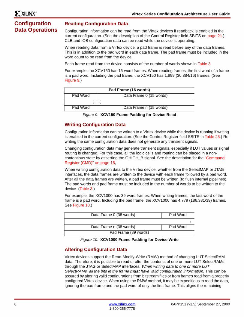
Virtex Series Configuration Architecture User GuideR13
ConfigurationData Operations
Reading Configuration DataConfiguration information can be read from the Virtex devices if readback is enabled in thecurrent configuration (See the description of the Control Register field SBITS on page 21)CLB and IOB configuration data can be read while the device is operating
When reading data from a Virtex device a pad frame is read before any of the data framesThis is in addition to the pad word in each data frame The pad frame must be included in theword count to be read from the device
Each frame read from the device consists of the number of words shown in Table 3
For example the XCV150 has 16-word frames When reading frames the first word of a frameis a pad word Including the pad frame the XCV150 has 1899 (3038416) frames (SeeFigure 9)
Writing Configuration DataConfiguration information can be written to a Virtex device while the device is running if writingis enabled in the current configuration (See the Control Register field SBITS in Table 23) Re-writing the same configuration data does not generate any transient signals
Changing configuration data may generate transient signals especially if LUT values or signalrouting is changed For this case all the logic cells and routing can be placed in a non-contentious state by asserting the GHIGH_B signal See the description for the CommandRegister (CMD) on page 18
When writing configuration data to the Virtex device whether from the SelectMAP or JTAGinterfaces the data frames are written to the device with each frame followed by a pad wordAfter all the data frames are written a pad frame must be written (to flush internal pipelines)The pad words and pad frame must be included in the number of words to be written to thedevice (Table 3)
For example the XCV1000 has 39-word frames When writing frames the last word of theframe is a pad word Including the pad frame the XCV1000 has 4779 (18638139) framesSee Figure 10)
Altering Configuration DataVirtex devices support the Read-Modify-Write (RMW) method of changing LUT SelectRAMdata Therefore it is possible to read or alter the contents of one or more LUT SelectRAMsthrough the JTAG or SelectMAP interfaces When writing data to one or more LUTSelectRAMs all the bits in the frame must have valid configuration information This can beassured by altering valid configurations from bitstream files or from frames read from a properlyconfigured Virtex device When using the RMW method it may be expeditious to read the dataignoring the pad frame and the pad word of only the first frame This aligns the remaining
Pad Frame (16 words)Pad Word Data Frame 0 (15 words)
hellip
hellip
Pad Word Data Frame n (15 words)
Figure 9 XCV150 Frame Padding for Device Read
Data Frame 0 (38 words) Pad Word
hellip
Data Frame n (38 words) Pad WordPad Frame (39 words)
Figure 10 XCV1000 Frame Padding for Device Write
8 wwwxilinxcom XAPP151 (v15) September 27 20001-800-255-7778
Virtex Series Configuration Architecture User GuideR13
configuration data in the Device Write format After modifying the configuration the altered datacan be written to the Virtex device followed by a pad word and a pad frame
It is not necessary to retain the contents of the pad frame or pad words However pad wordsand pad frames are included in the CRC calculation
Definitions Two sets of variables are defined to determine where a desired bit is in the configuration dataThe first is a set of ldquoindependentrdquo variables or design attributes namely characteristics of thedesign that are known ie the device size and which CLB and bit(s) within the CLB to locateTable 4 The second set is a set of ldquodependentrdquo variables or design variables namely valuesthat must be calculated to find the bit(s) of interest listed in Table 5
Note Frames span an entire column of CLB slices (or IOBs) Thus when changing LUTSelectRAM bit 0 for a single CLB slice (eg R3C4S1) LUT SelectRAM bit 0 for all slices inthat column (ie RC4S1) is written with the same command One must ensure that either allother data in the slice is constant or changed externally through partial configurations
LUT SelectRAMs not configured externally should not lie in the same slice with LUTs or LUTSelectRAMs that are re-configured externally Such a mixture can cause the unrelated LUTSelectRAM data to be re-configured when the frames are written to the device Figure 11shows what can happen if this restriction is not observed
In this example it is the objective to perform a Read-Modify-Write on the LUT SelectRAM inR2C3S1 in column 3 which is shown in the first column in the figure Row 2 contains a LUTcontaining the value AB Row 3 contains a SelectRAM containing the value C3 Because theRead and Write operations operate on an entire frame the RAM in R3C3S1 is also read andwritten when R2C3S1 is read and written Performing the Readback operation reads all theLUT and SelectRAM values for the column Before the new value for the LUT is written it ispossible for the on-chip circuitry to write a new value such as 14 into the SelectRAM Whenthe new value BD is written via the configuration interface into LUT R2C3S1 the value C3 isalso written into RAM R3C3S1 This may not always be desirable (It is design-dependent)
Figure 11 Potential Write Conflicts
x151_11_020800
LUT R2C3S113AB13
RAM R3C3S113C313
Before13Readback
13
LUT R2C3S113AB13
RAM R3C3S1131413
Before13Configuration 13
Write
13
LUT R2C3S113BD13
RAM R3C3S113C313
After13Configuration13
Write
13
Table 4 Design Attributes (Independent Variables)
Term Definition
Chip_Cols of CLB columns on the Virtex device
Chip_Rows of CLB rows on the Virtex device
Chip_Rams of block SelectRAM columns on the Virtex device
RAM_Space Spacing of block SelectRAM columns (in terms of CLB columns)
FL of 32-bit words in the frame
XAPP151 (v15) September 27 2000 wwwxilinxcom 91-800-255-7778
Virtex Series Configuration Architecture User GuideR13
RW 1 for Read 0 for Write
CLB_Col Column number of the desired CLB
CLB_Row Row number of the desired CLB
Slice 0 or 1
FG 0 for the F-LUT 1 for the G-LUT
lut_bit The desired bit from the given LUT Bits in the LUT are indexed from 0 to 15
XY 0 for the X Flip-Flop 1 for the Y Flip-Flop
RAM_Col Column number of the desired block SelectRAM
RAM_Row Row number of the desired block SelectRAM
ram_bit The desired bit from the given block SelectRAM Bits are indexed from 0 to4095
Table 5 Design Variables (Dependent Variables)
Term Definition
MJA Frame Major Address
MNA Frame Minor Address
fm_st_wd The index of the word within a full configuration segment that correspondsto the starting word of the desired frame A full configuration segment isdefined as the following 1) for CLBIOB all CLB IOB and RAMinterconnect frames beginning at MJA=0 MNA=0 and 2) for blockSelectRAM all RAM content frames for the given RAM column Words arenumbered starting at 0
fm_wd The index of the 32-bit word within a frame that contains the desired bitWords in a frame are numbered starting at 0
fm_wd_bit_idx The bit index of the desired bit within frame word fm_wd Words areindexed in ldquobig-endianrdquo style with bit 31 on the left and bit 0 on the right
fm_bit_idx Bit index within a frame of the desired bit Numbered starting with 0 as theleft-most (first) bit Bit numbering within a frame continues across all thewords in the frame
Table 6 Functions used in Equations
Functions Definition
floor(x) The largest integer not larger than x Eg floor(31) = 3 because the nextlargest integer 4 is larger than 31 floor(3)=3
ceiling(x) The smallest integer greater than or equal to x For example ceiling(32) = 4because 4 is greater than 32 and 3 is not ceiling (4) = 4
The modulus operation 5 2 = 1 5 3 = 2 5 5 = 0
Table 4 Design Attributes (Independent Variables) (Continued)
Term Definition
10 wwwxilinxcom XAPP151 (v15) September 27 20001-800-255-7778
Virtex Series Configuration Architecture User GuideR13
CLB LUTSelectRAMDependentVariables
Table 7 shows equations for the LUT SelectRAM ldquoDependent Variablesrdquo that were defined inTable 5
Virtex-E CLB LUT SelectRAM Dependent VariablesThe additional block SelectRAM columns in Virtex-E devices require an adjustment to the MJAThe following equations calculate the adjustment necessary for each of the affected dependentvariables For each variable calculate the base value based upon the Virtex equations onlyand then add the resulting Virtex adjustment
The left and right sides of the device are treated differently
LUT SelectRAM ExamplesSee ldquoExamplesrdquo on page 27 for several examples of reading and evaluating configuration dataThe examples illustrate how to make use of these equations to find the desired data in abitstream
Table 7 Virtex Equations for LUT SelectRAM Dependent Variables
Term Definition
MJA if (CLB_Col le Chip_Cols2)then Chip_Cols ndash CLB_Col times 2 + 2else 2 times CLB_Col ndash Chip_Cols ndash 1
MNA lut_bit + 32 ndash Slice times (2 times lut_bit + 17)
fm_bit_idx 3 + 18 times CLB_Row ndash FG + RW times 32
fm_st_wd FL times (8 + (MJA ndash1) times 48 + MNA) + RW times FL
fm_wd floor(fm_bit_idx32)
fm_wd_bit_idx 31 + 32 times fm_wd ndash fm_bit_idx
Notes
bull Do NOT input the final results back into the original Virtex equations (eg do not useMJAfinal value to calculate fm_st_wd)
bull MJAfinal = MJA + MJA_adj
bull fm_st_wdfinal = fm_st_wd + fm_st_wd_adj
Table 8 CLB Location
CLB Location CLB Column
Left CLB_Col le Chip_Cols2
Right CLB_Col gt Chip_Cols2
Table 9 Virtex-E Families Adjustments for LUT SelectRAM Dependent Variables
Term Definition
MJA_adj Left RAM_Bound = (Chip_Rams2 - 1) x RAM_SpaceMJA_adj = 2 x ceiling((RAM_Bound - CLB_Col + 1) RAM_Space)
Right
RAM_Bound = Chip_Cols - (Chip_Rams2 - 1) x RAM_Space + 1MJA_adj = 2 x ceiling((CLB_Col - RAM_Bound + 1) RAM_Space)
fm_st_wd_adj FL times (27 x MJA_adj)
XAPP151 (v15) September 27 2000 wwwxilinxcom 111-800-255-7778
Virtex Series Configuration Architecture User GuideR13
CLB Flip-FlopDependentVariables
Equations for the CLB flip-flops can be found in Table 10 Their locations are calculatedsimilarly to the LUT SelectRAM locations Equations for the CLB FF Dependent Variables aredefined in Table 5
Virtex-E CLB Flip-Flop Dependent VariablesApply the adjustments given in Table 8 and Table 9
IOB DependentVariables
Each IOB contains four values that can be captured into special registers These values are
bull I mdash the input flip-flop
bull O mdash the output flip-flop
bull T mdash the flip-flop for the tri-state control
bull P mdash the value of the IO pad
These values are captured by utilizing the CAPTURE_VIRTEX symbol in your design TheLibraries Guide has more details on the use of this symbol The following registers will be readas part of the readback data
Access to the IOB flip-flops is different for the top and bottom IOBs versus the left and rightIOBs
The top and bottom IOBs are part of the CLB column frames There are two IOBs at the top andbottom of each CLB column
The left and right IOBs are in columns by themselves There are three IOBs per CLB row
IOBs are numbered clockwise around the die Pad 1 is located at the left side of the top edgeabove CLB column 1 The equations for where to find IOB flip-flops in the bitstream are basedon the pad number which is the same for a given size device not the package pin name whichvaries from package to package The mapping from package pin names to pad numbers canbe found in EPIC or fpga_editor
Table 11 contains the numeric pad indices for the pads on all four edges of the device in termsof the number of CLB columns and rows on the device
Table 10 Virtex Equations for CLB FF Dependent Variables
Term Definition
MJA if (CLB_Col le Chip_Cols2)then Chip_Cols ndash CLB_Col times 2 + 2else 2 times CLB_Col ndash Chip_Cols ndash 1
MNA Slice times (12 times XY ndash 43) ndash 6 times XY + 45
fm_bit_idx (18 times CLB_Row) + 1 + (32 times RW)
fm_st_wd FL times (8 + (MJA ndash1) times 48 + MNA) + RW times FL
fm_wd floor(fm_bit_idx32)
fm_wd_bit_idx 31 + 32 times fm_wd ndash fm_bit_idx
12 wwwxilinxcom XAPP151 (v15) September 27 20001-800-255-7778
Virtex Series Configuration Architecture User GuideR13
Table 12 shows the equations for the dependent variables for the IOB flip-flops The variable iin this table refers to the index of pad i
Table 11 IOB Pad Indices
PadLocation Pad Index i
Top 1 le i le Chip_Cols times 2
Right Chip_Cols times 2 +1 le i le Chip_Cols times 2 + Chip_Rows times 3
Bottom Chip_Cols times 2 + Chip_Rows times 3 + 1 le i le Chip_Cols times 4 + Chip_Rows times 3
Left Chip_Cols times 4 + Chip_Rows times 3 + 1 le i le Chip_Cols times 4 + Chip_Rows times 6
Table 12 Equations for IOB Dependent Variables
Term Definition
MJA
Topif (i le Chip_Cols)then Chip_Cols ndash ceiling(i2) times 2 + 2else 2 times ceiling (i2) ndash Chip_Cols ndash1
Right Chip_Cols + 1
Bottomif (i gt 3 times (Chip_Cols + Chip_Rows))then 2 times ceiling((i ndash 3 times Chip_Cols ndash 3 times Chip_Rows)2)else Chip_Cols ndash 2 times floor((i ndash 2 times Chip_Cols ndash 3 times Chip_Rows ndash 1)2) ndash 1
Left Chip_Cols + 2
MNA
Top
I ndash 25 times (i2) + 45
O ndash 13 times (i2) + 39
T ndash 5 times (i2) + 35
P ndash 4 times (i2) + 25
Right
I t = (i ndash 2 times Chip_Cols) 3 MNA = 275 times t2 ndash 575 times t + 32
O t = (i ndash 2 times Chip_Cols) 3 MNA = 215 times t2 ndash 515 times t + 38
T t = (i ndash 2 times Chip_Cols) 3 MNA = 175 times t2 ndash 475 times t + 42
P 50
Bottom
I 25 times ((i ndash 2 x Chip_Cols - 3 x Chip_Rows)2) + 20
O 13 times ((i ndash 2 x Chip_Cols - 3 x Chip_Rows)2) + 26
T 5 times ((i ndash 2 x Chip_Cols - 3 x Chip_Rows)2) + 30
P 4 times ((i ndash 2 x Chip_Cols - 3 x Chip_Rows)2) + 21
Left
I t = (i ndash 4 x Chip_Cols - 3 x Chip_Rows)3 MNA = 175 times t2 ndash 475 times t + 45
O t = (i ndash 4 x Chip_Cols - 3 x Chip_Rows)3 MNA = 235 times t2 ndash 535 times t + 39
T t = (i ndash 4 x Chip_Cols - 3 x Chip_Rows)3 MNA = 275 times t2 ndash 575 times t + 35
P 50
XAPP151 (v15) September 27 2000 wwwxilinxcom 131-800-255-7778
Virtex Series Configuration Architecture User GuideR13
Virtex-E IOB Dependent VariablesSimilar to CLB dependent variables only the variables affected by the major address aredifferent in Virtex-E and Virtex-EM devices versus Virtex devices A simple way to account forthe change is to determine the CLB column where the pad resides (only true for top andbottom) Then the adjustment calculated for the CLB column can be applied The conversionto CLB columns is found in Table 13
fm_bit_idx
Top 32 times RW
Right
I O ampT 18 times (1 + floor ((i ndash 2 times Chip_Cols ndash 1)3)) + 32 times RW
Pt = (i ndash 2 times Chip_Cols) 3fm_bit_idx = 18 times (1 + floor ((i ndash 2 times Chip_Cols ndash 1)3)) + 6 times t2 ndash 17 times t + 15 + 32 timesRW
Bottom 18 times (Chip_Rows + 1)+ 32 times RW
Left
I O ampT18 times (Chip_Rows ndash floor((i ndash 4 times Chip_Cols ndash 3 times Chip_Rows ndash 1)3)) + 32 times RW
Pt = (i ndash 4 times Chip_Cols ndash 3 times Chip_Rows)3fm_bit_idx = 18 times (Chip_Rows ndash floor ((i ndash 4 times Chip_Cols ndash 3 times Chip_Rows ndash 1)3))ndash 105 times t2 + 215 times t + 4 + 32 times RW
fm_st_wdif (MJA gt Chip_Cols + 1)then FL times (54 times MJA ndash 46 + MNA ndash 6 times Chip_Cols) + RW times FLelse FL times (8 + (MJA ndash1) times 48 + MNA) + RW times FL
fm_wd floor (fm_bit_idx32)
fm_wd_bit_idx 31 + 32 times fm_wd ndash fm_bit_idx
Table 12 Equations for IOB Dependent Variables (Continued)
Term Definition
Table 13 Pad -gt CLB Column
Term Definition
CLB_ColTop ceiling(i2)
Bottom ceiling((4 x Chip_Cols + 3 x Chip_Rows + 1 - i)2)
Table 14 Virtex-E Families Adjustments for IOB Dependent Variables
Term Definition
MJA_adj
Top use Table 8 and Table 9
Right Chip_Rams
Bottom use Table 8 and Table 9
Left Chip_Rams
fm_st_wd_adj FL times (27 x MJA_adj)
14 wwwxilinxcom XAPP151 (v15) September 27 20001-800-255-7778
Virtex Series Configuration Architecture User GuideR13
BlockSelectRAMDependentVariables
The equations for the block SelectRAM dependent variables are given in Table 15 Therelationship of a particular memory cell index in the context of a given configuration is describedin XAPP130 ldquoUsing the Vir tex Bloc k SelectRAM+ Resour cerdquo
Virtex-E Block SelectRAM Dependent VariablesThe RAM major address numbering scheme changed slightly such that the lowest MJA on theleft side is now 2 instead of 0 As in the case for the CLB equations the adjustments belowshould be applied after the Virtex equations
Table 15 Virtex Equations for Block SelectRAM Dependent Variables
Term Definition
MJAif (RAM_Col lt Chip_Rams2)then 2 x (Chip_Rams2 - 1 - RAM_Col)else 2 x (RAM_Col - Chip_Rams2) + 1
MNA
1 x floor(((ram_bit 64) 64)32) + 2 x floor(((ram_bit 64) 32)16)+ 4 x floor(((ram_bit 64) 16)8) + 8 x floor(((ram_bit 64) 8)4)+ 16 x floor(((ram_bit 64) 4)2) + 32 x floor(((ram_bit 64) 2)1)equivalent to MNA = div64[05] where div64[50] = floor(ram_bit64)
fm_bit_idxobtain value for bitpos from Table 16
fm_bit_idx = 18 + 72 x RAM_Row + bitpos
fm_st_wd FL times MNA + RW times FL
fm_wd floor(fm_bit_idx32)
fm_wd_bit_idx 31 + 32 times fm_wd ndash fm_bit_idx
Table 16 Virtex Block SelectRAM Bit Position Within a Given Block SelectRAM
ram
_bit
6
4
bitp
os
ram
_bit
6
4
bitp
os
ram
_bit
6
4
bitp
os
ram
_bit
6
4
bitp
os
ram
_bit
6
4
bitp
os
ram
_bit
6
4
bitp
os
ram
_bit
6
4
bitp
os
ram
_bit
6
4
bitp
os
0 42 8 45 16 29 24 26 32 43 40 44 48 28 56 27
1 58 9 61 17 13 25 10 33 59 41 60 49 12 57 11
2 41 10 46 18 30 26 25 34 40 42 47 50 31 58 24
3 57 11 62 19 14 27 9 35 56 43 63 51 15 59 8
4 50 12 53 20 21 28 18 36 51 44 52 52 20 60 19
5 49 13 54 21 22 29 17 37 48 45 55 53 23 61 16
6 66 14 69 22 5 30 2 38 67 46 68 54 4 62 3
7 65 15 70 23 6 31 1 39 64 47 71 55 7 63 0
Table 17 Virtex-E and Virtex-EM Adjustments for Block SelectRAM DependentVariables
Term Definition
MJA_adj if (RAM_Col lt Chip_Rams2) MJA_adj = 2
XAPP151 (v15) September 27 2000 wwwxilinxcom 151-800-255-7778
Virtex Series Configuration Architecture User GuideR13
ConfigurationLogic Basics
Configuration DataConfiguration data is organized as 32-bit words There are two major commands that theconfiguration data can contain Read and Write A configuration command is executed whenthe configuration command is read or written to the appropriate command register
The OP field contains 01 for a Read operation and 10 for a Write operation (See Figure 12)
A command is organized as a packet with a header word and optional data words The headerword is the first word written to the appropriate command register for a read or write operationThe header word contains a type field (001) an operand field a register address field and aword count field The format for the command header is shown in Figure 13 on page 17
The Register Address field defines the target of this command as defined in Table 18 on page17
The header word count field contains an integer between 0 and 2047 and indicates thenumber of words that follow the header Larger word counts (between 2048 and 1048575words) are achieved by setting the header word count to 0 The Extension header word has atype field = 010 an OP field that must match the OP field in the preceding Command Headerword and a 20-bit word count this format is shown Figure 14 on page 17
Configuration FlowVirtex devices are configured by presenting configuration data to the SelectMAP or JTAGinterfaces in a specific sequence
For Initial Configuration
1 Issue one or more pad words (SelectMAP only)
2 Issue Sync word (SelectMAP only)
3 Reset CRC
4 Set FLR
5 Set COR
6 Set MASK
7 Set CTL (Set PERSIST if you want to keep SelectMAP active after this configuration)
8 Issue a SWITCH (switch CCLK frequency) command to the CMD register This isnecessary only in Master Serial configuration mode
Reading Configuration
These commands can be issued to read a full configuration or for a partial configuration afterthe device has been completely configured
1 Issue a Sync word (SelectMAP only) if the previous configuration command was aborted
2 Set the FAR to the starting address
3 Issue a RCFG (read configuration) command to the CMD register
4 Write the number of words to be read to the FDRO register
5 Flush the command pipeline with a pad word
6 Read data frames
OP CODERead 01Write 10
Figure 12 OP Field Code
16 wwwxilinxcom XAPP151 (v15) September 27 20001-800-255-7778
Virtex Series Configuration Architecture User GuideR13
Writing Configuration
These commands can be issued either as part of an initial configuration or for a partialconfiguration after the device has been configured
1 Issue a Sync word (SelectMAP only) if the previous configuration command was aborted
2 If the frames being written can cause contention then assert the GHIGH_B signal
3 Set the FAR to the starting address
4 Issue a WCFG (write configuration) command to the CMD register
5 Write the number of words to be written to the FDRI register
6 Write data frames
7 If the GHIGH_B signal was asserted de-assert it by writing the LFRM (Last Frame)command to the CMD register and write one pad frame
ConfigurationRegisters
Configuration logic is accessed and controlled via a collection of 32-bit registers called theconfiguration registers (see Table 18) Registers are described in the following sections
Type OP Register Address RSV Word Count31 30 29 28 27 26 25 24 23 22 21 20 19 18 17 16 15 14 13 12 11 10 9 8 7 6 5 4 3 2 1 00 0 1 x x 0 0 0 0 0 0 0 0 0 0 x x x x 0 0 x x x x x x x x x x x
Notes1 Locations within fields containing a zero or one must have these values An X in a bit field indicates that the value is variable and must
be set2 Heavy vertical lines are used to separate fields Light vertical lines separate nibbles in the word
Figure 13 Command Header Format
Type OP Word Count31 30 29 28 27 26 25 24 23 22 21 20 19 18 17 16 15 14 13 12 11 10 9 8 7 6 5 4 3 2 1 00 1 0 x x 0 0 0 0 0 0 0 x x x x x x x x x x x x x x x x x x x x
Notes1 Locations within fields containing a zero or one must have these values An X in a bit field indicates that the value is variable and must
be set2 Heavy vertical lines are used to separate fields Light vertical lines separate nibbles in the word
Figure 14 Large Block Count Header Extension Format
Table 18 Configuration Register Addresses
Register Name Mnemonic RW Binary Address
CRC CRC RW 0000
Frame Address FAR RW 0001
Frame Data Input FDRI W 0010
Frame Data Output FDRO R 0011
Command CMD RW 0100
Control CTL RW 0101
Control Mask MASK RW 0110
Status STAT R 0111
Legacy Output LOUT W 1000
XAPP151 (v15) September 27 2000 wwwxilinxcom 171-800-255-7778
Virtex Series Configuration Architecture User GuideR13
Command Register (CMD)The content of the Command Register (CMD) is interpreted by the configuration state machineConfiguration commands control the operation of the configuration state machine the FrameData Register (FDR) and some of the global signals The command in the Command Registeris executed each time the FAR is loaded with a new value The effect of each command isdefined in Table 19
Configuration Option COR RW 1001
Reserved mdash mdash 1010
Frame Length FLR RW 1011
Reserved mdash mdash 1100
Reserved mdash mdash 1101
Reserved mdash mdash 1110
Reserved mdash mdash 1111
Table 18 Configuration Register Addresses (Continued)
Register Name Mnemonic RW Binary Address
Table 19 Configuration Commands
Cmd Code Description
Rsvd 0000 Reserved
WCFG 0001Write Configuration Data mdash Used prior to writing configuration data to the FDRI It takes theinternal configuration state machine through a sequence of states that control the shifting of the FDRand the writing of the configuration memory (See Frame Data Input Register (FDRI) on page 24)
Rsvd 0010 Reserved
LFRM 0011Last Frame mdash This command is loaded prior to writing the last (pad) data frame if the GHIGH_Bsignal was asserted This command is not necessary if the GHIGH_B signal was not asserted Thisallows overlap of the last frame write with the release of the GHIGH_B signal
RCFG 0100Read Configuration Data mdash Used prior to reading frame data from the FDRO Similar to the WCFGcommand in its effect on the FDR (see Frame Data Output Register (FDRO) on page 24)
START 0101Begin Startup Sequence mdash Starts the startup sequence This command is also used to start ashutdown sequence prior to partial re-configuration The Startup Sequence begins with the nextsuccessful CRC check (see Cyclic Redundancy Check (CRC) on page 22)
RCAP 0110Reset Capture mdash Used when performing capture in single-shot mode This command must be usedto reset the capture signal if single-shot capture has been selected
RCRC 0111 Reset CRC mdash Used to reset CRC register (see Cyclic Redundancy Check (CRC) on page 22)
AGHIGH 1000Assert GHIGH_B Signal mdash Used prior to re-configuration to prevent contention while writing newconfiguration data All CLB outputs and signals are forced to a one
SWITCH 1001Switch CCLK Frequency mdash Used to change (increase) the frequency of the Master CCLK Thenew frequency is specified in Table 21
Rsvd 1010 Reserved
Rsvd 1011 Reserved
Rsvd 1100 Reserved
18 wwwxilinxcom XAPP151 (v15) September 27 20001-800-255-7778
Virtex Series Configuration Architecture User GuideR13
Configuration Option Register (COR)The Configuration Option Register (COR) is used to select configuration options that areillustrated in Figure 15 and defined in Table 20 Entries in this table are further explained in thefollowing tables
Rsvd 1101 Reserved
Rsvd 1110 Reserved
Rsvd 1111 Reserved
Table 19 Configuration Commands (Continued)
Cmd Code Description
DO
NE
_PIP
E
DR
IVE
_DO
NE
SIN
GLE
OS
CF
SE
L
SS
CLK
SR
C
LOC
K_W
AIT
SH
UT
DO
WN
DO
NE
_CY
CLE
LCK
_CY
CLE
GT
S_C
YC
LE
GW
E_C
YC
LE
GS
R_C
YC
LE
31 30 29 28 27 26 25 24 23 22 21 20 19 18 17 16 15 14 13 12 11 10 9 8 7 6 5 4 3 2 1 00 x x x x x x x x x x x x x x x x x x x x x x x x x x x x x x x
Notes1 Locations within fields containing a zero or one must have these values An X in a bit field indicates that the value is variable and must
be set2 Heavy vertical lines are used to separate fields Light vertical lines separate nibbles in the word
Figure 15 COR (Configuration of Option Register) Fields
XAPP151 (v15) September 27 2000 wwwxilinxcom 191-800-255-7778
Virtex Series Configuration Architecture User GuideR13
Table 21 shows the allowed values for the OSCFSEL field of the COR Setting OSCFSEL toone of these values will set the Master CCLK frequency to the specified value
Table 20 Configuration Option Register Fields
Field Bit Indices DescriptionBitgenDefault
DONE_PIPE 30
0 No pipeline stage for DONEIN
1 Add pipeline stage to DONEINFPGA waits on DONE that is delayed by one (1) cycle of the StartupClkrather than the pin itself Use this option when StartupClk is running at highspeeds
0
DRIVE_DONE 290 DONE pin is open drain
1 DONE pin is actively driven high0
SINGLE 28 Readback capture is one-shot 0
OSCFSEL 2722 Select CCLK frequency in Master Serial configuration mode 2
SSCLKSRC 2120
Startup sequence clock source00 Cclk01 UserClk1x JTAGClk
0
LOCK_WAIT 1916
4-bit mask indicating which DLL lock signals to wait for during LCK cycleThe 4 bits (from MSB to LSB) correspond to DLLs TL=3 TR=2 BL=1BR=0 (top-left top-right etc) In Virtex-E devices where there are 8 DLLseach mask bit applies to the 2 DLLs in that quadrant of the device Thedefault is not to wait for any DLL lock signals
0
SHUTDOWN 15
Indicate whether doing a startup or shutdown sequence
0 Startup
1 Shutdown sequence
0
DONE_CYCLE 1412 Startup phase in which DONE pin is released 3
LCK_CYCLE 119 Stall in this startup phase until DLL locks are asserted 7
GTS_CYCLE 86 Startup phase in which IOs switch from tri-state to user design 4
GWE_CYCLE 53 Startup phase in which the global write-enable is asserted 5
GSR_CYCLE 20 Startup phase in which the global setreset is negated 5
Table 21 OSCFSEL-Specified Master CCLK Frequencies)
CCLK(MHz) OSCFSEL
CCLK(MHz) OSCFSEL
CCLK(MHz) OSCFSEL
43 000010 13 001010 41 100111
54 010001 15 001101 45 110011
69 000100 20 010111 51 101010
81 000101 26 011010 55 110100
20 wwwxilinxcom XAPP151 (v15) September 27 20001-800-255-7778
Virtex Series Configuration Architecture User GuideR13
Table 22 shows the values of the DONE_CYCLE LCK_CYCLE GTS_CYCLE GWE_CYCLEand GSR_CYCLE fields in COR This table shows the step in the start-up sequence when eachof these signals becomes active
Control Register (CTL)The Control Register (CTL) fields are illustrated in Figure 16 on page 21 and defined inTable 23
92 000110 30 011101 60 101101
100 000111 34 110010 mdash mdash
Notes1 These values are accurate to +45 ndash 30
Table 22 COR Startup Cycle Fields
FieldValue
DONE_CYCLE(DONE Active)
GTS_CYCLE(GTS_CFGInactive)
GSR_CYCLE(GSR Inactive)
GWE_CYCLE(GWE Active) LCK_CYCLE
000 1 1 1 1 0
001 2 2 2 2 1
010 3 3 3 3 2
011 4 (default) 4 4 4 3
100 5 5 (default) 5 5 4
101 6 6 6 (default) 6 (default) 5
110 mdash DoneIndagger DoneIndagger DoneIndagger 6
111 Keep State Keep State Keep State Keep State Donrsquot Wait(default)
Notes1 dagger DONE if DonePipe = No else the delayed version of DONE
Table 21 OSCFSEL-Specified Master CCLK Frequencies) (Continued)
CCLK(MHz) OSCFSEL
CCLK(MHz) OSCFSEL
CCLK(MHz) OSCFSEL
SB
ITS
PE
RS
IST
GT
S_U
SR
_B
31 30 29 28 27 26 25 24 23 22 21 20 19 18 17 16 15 14 13 12 11 10 9 8 7 6 5 4 3 2 1 00 0 0 0 0 0 0 0 0 0 0 0 0 0 0 0 0 0 0 0 0 0 0 x x x 0 0 0 0 0 x
Notes1 Locations within fields containing a zero or one must have these values An X in a bit field indicates that the value is variable and must
be set2 Heavy vertical lines are used to separate fields Light vertical lines separate nibbles in the word
Figure 16 Control Register Fields
XAPP151 (v15) September 27 2000 wwwxilinxcom 211-800-255-7778
Virtex Series Configuration Architecture User GuideR13
Cyclic Redundancy Check (CRC)A data input error checking mechanism is provided through the Cyclic Redundancy Check(CRC) register When data is written to any configuration register (except LOUT) a 16-bit CRCvalue is calculated using both the register data and the address This value is saved in the CRCregister At the end of any series of writes a pre-calculated CRC block-check value may bewritten to the CRC register If the resulting value is non-zero an error is indicated TheCRC_ERROR bit is accessible through the status register If a CRC error is detectedconfiguration logic is put in the ERROR mode The following section is an algorithm forcomputing CRC
CRC Algorithm Initialization bcc = 0skip_pad = truemore_words = true Check for write operation do
w = next_wordif (w[3127] == rsquo00101rsquo)
A Read OP Donrsquot use in CRCwc = w[100]if (wc == 0)
w = next_wordwc = w[190]
while (wc-- gt 0)
w = next_word
elsif (w[3127] == rsquo00110rsquo)
A Write OP Use in CRC addr = w[1613]if (addr Π0124569DB)
wc = w[100]if (wc == 0)
wc is in next word w = next_wordwc = w[190]
while (wc-- gt 0)
w = next_wordsw[350] = addr wordfor (i=0 ilt36 i++)
Table 23 Control Register Bits
NameBit
Indices Description
SBITS 87 Security level0 ReadWrite OK (default)1 Readback disabled23 Readback disabled Writing disabled except CRCregister
PERSIST 6 Configuration interface remains after configuration0 No (default)1 Yes
GTS_USR_B 0 Active-low global tristate IOs Turn off pull-ups ifGTS_CFG_B is also asserted
22 wwwxilinxcom XAPP151 (v15) September 27 20001-800-255-7778
Virtex Series Configuration Architecture User GuideR13
x16 = bcc[15] XOR sw[i]x15 = bcc[14] XOR x16x2 = bcc[1] XOR x16bcc[150] =
x15bcc[132]x2bcc[0]x16 Note the bit order crc[150] = bcc[015]
else
Pad word - ignore
while (more_words)
Frame Address Register (FAR)The Frame Address Register (FAR) holds the address of the current frame The address isdivided into three parts the block type the major address and the minor address The blocktype field indicates whether the CLB or block RAM address space is used The command in thecommand register is executed each time the FAR is loaded with a new value
The major address selects the CLB or RAM column the minor address selects the frame withinthe column The minor address is incremented each time a full data frame is read from orwritten to the frame data register If the last frame within the CLB column is selected when theincrement occurs the major address is incremented and the minor address is reset to zerootherwise the minor address is incremented However the block RAM major address is notincremented automatically
See Figure 18 for the definitions of valid values for the block type field The FAR field definitionsare shown in Figure 19
Figure 17 CRC Calculation Register
Note the Block RAM Major Address is not incremented automatically To address a differentBlock RAM Content column the FAR must be loaded with the new Major Address
Type CodesCLB 00RAM 01
Figure 18 Block Type Codes
x151_17_021100
15141312111098765432
1013
01234526272829303101
Address 32-bit Data Word
CRC Calculation Register
CRC Data Input Register
CRC Register [310]
DATA_IN
SHIFT
23
16-bit CRC13150
0000 0000 0000 0000133116
1313
XAPP151 (v15) September 27 2000 wwwxilinxcom 231-800-255-7778
Virtex Series Configuration Architecture User GuideR13
Frame Data Input Register (FDRI)The Frame Data Input Register (FDRI) is used to load configuration frame data into a Virtexdevice
The Frame Data Register (FDR) is a shift register into which data is loaded prior to transfer tothe configuration memory Configuration data is written to the Virtex device by loading thecommand register with the WCFG command and then loading the FDR with at least two framesof 32-bit words
The write operation is pipelined such that the first frame of data is written to the configurationmemory while the second frame is being shifted in The last frame (the pad frame) is alwaysdummy data which is not actually written to the configuration memory Each frame write mustinclude enough 32 bit data words to load the frame fully There is one pad word at the end ofeach frame which is required for the pipelining hardware
Frame Data Output Register (FDRO)The Frame Data Output Register (FDRO) is for reading configuration data or captured datafrom the Virtex device a process called readback Readback is performed by loading thecommand register with the RCFG command and then addressing the FDRO with a readcommand
Frame Length Register (FLR)Near the beginning of the configuration bitstream the Frame Length Register (FLR) is writtenwith the length of a frame as measured in 32-bit words This length count is used to providesequencing information for the configuration read and write operations Note that the FLR mustbe written before any FDR operation works It is not necessary to set the FLR more than onceIf the number of bits in a frame is not evenly divisible by 32 the length count of the frame mustbe rounded up to the next highest integer The values for the FLR for all the current Virtexseries devices are given in Table 24
BlockType
Major Address(Column Address)
Minor Address(Frame Address)
31 30 29 28 27 26 25 24 23 22 21 20 19 18 17 16 15 14 13 12 11 10 9 8 7 6 5 4 3 2 1 00 0 0 0 0 x x x x x x x x x x x x x x x x x x 0 0 0 0 0 0 0 0 0
Notes1 Locations within fields containing a zero or one must have these values An X in a bit field indicates that the value is variable and must
be set2 Heavy vertical lines are used to separate fields Light vertical lines separate nibbles in the word
Figure 19 Frame Address Fields (FAR)
Note The FLR contains a value that is one less than the number of words that are read fromor written to a given frame This is because the extra word needed for pipelining is not counted
Table 24 Frame Length Register Value
Device Row times Col Frame Length Words per Frame FLR Value
XCV50E 16 times 24 384 12 11
XCV100E 20 times 30 448 14 13
XCV150 24 times 36 512 16 15
XCV200E 28 times 42 576 18 17
XCV300E 32 times 48 672 21 20
24 wwwxilinxcom XAPP151 (v15) September 27 20001-800-255-7778
Virtex Series Configuration Architecture User GuideR13
Legacy Output Register (LOUT)The Legacy Output Register (LOUT) is used for daisy chaining the configuration bitstream toother Xilinx devices Data written to the LOUT is serialized and appears on the DOUT pin
Mask Register (MASK)The Mask Register (MASK) is a mask register for writes to the CTL register A 1 in bit N of themask allows that bit position to be written in the CTL register The default value of the mask isall 0s
Status Register (STAT)The Status Register (STAT) is loaded with current values of several control or status signalsThe register can be read via the re-configuration block or via JTAG The fields in the Statusregister are illustrated in Figure 20 The values of the signals given in Table 25 on page 26 canbe read from the status register
XCV400E 40 times 60 800 25 24
XCV405E 40 times 60 800 25 24
XCV600E 48 times 72 960 30 29
XCV800 56 times 84 1088 34 33
XCV812E 56 times 84 1088 34 33
XCV1000E 64 times 96 1248 39 38
XCV1600E 72 times 108 1376 43 42
XCV2000E 80 times 120 1536 48 47
XCV2600E 92 times 138 1728 54 53
XCV3200E 104 times 156 1952 61 60
Table 24 Frame Length Register Value (Continued)
Device Row times Col Frame Length Words per Frame FLR Value
DO
NE
INIT
MO
DE
GH
IGH
_B
GS
R_B
GW
E_B
GT
S_C
FG
IN_E
RR
OR
LOC
K
CR
C_E
RR
OR
31 30 29 28 27 26 25 24 23 22 21 20 19 18 17 16 15 14 13 12 11 10 9 8 7 6 5 4 3 2 1 00 0 0 0 0 0 0 0 0 0 0 0 0 0 0 0 0 x x x x x x x x x x x x x x x
Notes1 An X in a bit field indicates that the value is variable2 Heavy vertical lines are used to separate fields Light vertical lines separate nibbles in the word
Figure 20 Status Register Fields
XAPP151 (v15) September 27 2000 wwwxilinxcom 251-800-255-7778
Virtex Series Configuration Architecture User GuideR13
ConfigurationInterface
There are two configuration interfaces to the Virtex devices mdash the bit-serial Boundary Scaninterface and the 8-bit byte-serial SelectMAP interface Conceptually XCV50 configurationdata appears as in Figure 21
Frames and words within frames are written in the same order in both configuration interfacesstarting with Frame 0 word 0 (the left-most in the picture) followed by word 1 etc Bits withineach word are written from left to right (MSB first) in the bit-serial configuration interfaces
Within the SelectMAP interface data is written a byte at a time A sample word is shown inFigure 22 The top row indicates the device pin names The bottom row indicates the bit indiceswithin a configuration word Byte 0 loads first followed by byte 1 et cetera The MSB of eachbyte (ie bits 31 23 15 and 7) is loaded on pin D0 The LSB of each byte (ie bits 24 16 8and 0) is loaded on pin D7
PartialReconfigurationof CLBs
Partial reconfiguration can be performed with and without shutting down the device Ifcontention occurs it is advised to go through a shutdown sequence prior to loadingconfiguration frames When shutting down the DONE pin will go active and pull low If this is notdesireable the DONE pin can be prevented from going low by selecting the DONE_CYCLE toKeep State (111) Similarly to prevent GSR from becoming active and reseting the currentstate the GSR_CYCLE can be set to Keep State When not shutting down changes occurframe by frame but is completely done by the end of the Last Frame packet (see Example 1)
Table 25 Status Register Bits
Name Bit Indices Description
DONE 14 Input from DONE pin
INIT 13 Value of INIT
MODE 1210 Value of M2 M1 M0 mode pins
GHIGH_B 9 0 = GHIGH_B asserted
GSR_B 8 0 = all flip-flops are ResetSet
GWE_B 7 1 = flip-flops and block RAM are write disabled
GTS_CFG 6 0 = IOs are tri-stated
IN_ERROR 5 Legacy input error
LOCK 41 Output from DLL lock signals 1 = DLL is locked
CRC_ERROR 0 Indicates that a CRC error has occurred
Data Frame 0 (11 words) Pad Word
hellip
Data Frame n (11 words) Pad WordPad Frame (12 words)
Figure 21 XCV50 Frame Padding for Reads
Figure 22 SelectMAP Byte and Bit Ordering
x151_22_021100
D0 D1 D2 D3 D4 D5 D6 D7 D0 D1 D2 D3 D4 D5 D6 D7 D0 D1 D2 D3 D4 D5 D6 D7 D0 D1 D2 D3 D4 D5 D6 D7
Byte 0 Byte 1 Byte 2 Byte 313
26 wwwxilinxcom XAPP151 (v15) September 27 20001-800-255-7778
Virtex Series Configuration Architecture User GuideR13
The DONE pin will not change in this case Figure 23 illustrates a typical shutdownreconfiguration in the CLB address space and restart sequence
Examples Several examples of reading and evaluating configuration data are provided to illustrate thefollowing
Figure 23 Typical Shutdown Reconfiguration in the CLB Address Spaceand Restart Sequence
FFFF FFFF Dummy WordAA99 5566 Sync Word Does not realign an already synchronized SelectMap port3001 2001 COR0080 FF2F Shutdown bit set optionally set bit 29 DRIVE_DONE
Alternately COR may be read bit 15 set and written back3000 8001 CMD0000 0005 Start Shutdown3000 8001 CMD0000 0007 Reset CRC0000 00000000 0000 Clock shutdown sequence0000 00000000 00003000 8001 CMD0000 0008 Assert GHIGH3000 8001 CMD0000 0001 Write Configuration3000 2001 FAR0--- ---- Block Type CLB (00) MajorMinor Address3000 4--- FDRI + Word Count if count is lt1024 Otherwise use TypeII Header
Write FRAME DATAIf CLB Frames are not written to non-consecutive addresses repeat FAR word followedby new MajorMinor Address followed by FDRI + Word Count and then Frame Data
3000 0001 Write CRC---- ---- CRC3000 8001 CMD0000 0003 LFRM3000 4--- FDRI + Word Count
Write PAD FRAME
3001 2001 COR0080 3F2D Default COR Options
Alternately COR may be read bit 15 cleared and written back3000 8001 CMD0000 0005 Begin Startup3000 0001 Write CRC---- ---- CRC
0000 00000000 0000 4 Dummy Words0000 00000000 0000
Example 1 Read and Write Semaphores in an XCV100 at CLB R1 C1 Slice 0 on page 28Example 2 Reading the Complete Configuration from an XCV50 on page 33
XAPP151 (v15) September 27 2000 wwwxilinxcom 271-800-255-7778
Virtex Series Configuration Architecture User GuideR13
Example 1 Read and Write Semaphores in an XCV100 at CLB R1 C1Slice 0Semaphores are a useful communication mechanism documented in XAPP 153 ldquoStatus andControl Semaphore Registers using Partial Reconfigurationrdquo Figure 24 shows an abstractionof a microprocessor writing control information to an FPGA and reading status informationOne convention for implementing semaphores in Virtex devices is to use two bits of a 16-bitdual-port RAM as illustrated in Figure 25 This occupies one CLB slice with the F-LUTimplementing the control semaphore and the status semaphore implemented in the G-LUTAddress 15 of the G-LUT is used for on-chip writes to the semaphore and address 14 of the F-LUT is used for on-chip reads Conversely the off-chip microprocessor is reading the G-LUT[15] and writing F-LUT[14]
Example 3 Read the Slice 0 G-LUT from CLB R1 C1 from the Complete Configuration of anXCV50 on page 34Example 4 Read the Slice 1 F-LUT from CLB R19 C16 from an XCV100 on page 36Example 5 Read All Bits in Slice 0 G-LUTs from CLB C2 and XCV50 on page 39Example 6 Read Block SelectRAM index 387 of RAM R2 C0 from an XCV100E on page 41
Figure 24 Semaphore Abstraction
x151_ 23_021400
Status13
Control13
MicroProcessor FPGA13
Semaphores13
28 wwwxilinxcom XAPP151 (v15) September 27 20001-800-255-7778
Virtex Series Configuration Architecture User GuideR13
Using a Semaphore Abstraction dual-port RAM ensures that the LUT SelectRAMs are placedin the CLB in a predictable manner When writing data to one or more LUT SelectRAMs or flip-flops on the device all bits in the frame must have valid configuration information This isassured by altering valid configurations from bitstream files or from frames read from a properlyconfigured Virtex device The latter approach is used in this example
Figure 25 Semaphore ReadWrite Implementation
Frame 47
15
14
47 46
47 46
x151_ 24_021100
Select Map
Frame 46
DING
F
13
D2D3D4 5D6 7D0D1 D D
1
111
0
111
Chip Interface
G F
13
XAPP151 (v15) September 27 2000 wwwxilinxcom 291-800-255-7778
Virtex Series Configuration Architecture User GuideR13
Attributes for this design are summarized in Table 26
From the equations in Table 7 on page 11 the values shown in Table 27 can be calculated
From off-chip for reading the G-LUT[15] bit read one frame (MNA=47) For writing the F-LUT[14] bit we show how to read then write one frame (MNA=46) as opposed to modifyingdata from a bitstream file (both are valid methods) The frames on the XCV100 contain 13 32-bit words and one pad word Remember that fm_st_wd is calculated assuming the entireconfiguration has been read However only the pad frame and then frames 46 and 47 fromMajor Address 30 are being read The desired bit is in Frame 1 word 1 which is word 15
The commands for reading both frames (and the pad frame) are given in Figure 26
Table 26 Design Attributes for Example 1
Attribute
G-LUT [15] F-LUT [14]
Read Read Write
Chip_Rows 20
Chip_Cols 30
FL 14
CLB_Row 1
CLB_Col 1
Slice 0
FG 1 0
lut_bit 15 14
RW 1 1 0
Table 27 Semaphore Example Variables Equations and Values
Variable Equation
Value(s)
G-LUT[15] F-LUT[14]
Read Read Write
MJA 1 le 302 rArr 30 ndash 1 times 2 + 2 30
MNA lut_bit + 32ndash 0 times () 47 46
fm_bit_idx 3 + 18 times 1 ndash FG + RW times 32 52 53 21
fm_st_wd 14 times (8 + (30 ndash 1) times 48+ 4647) +RW times (14 +1)= 14 times (1400 + 4647) + 14 times RW= 19600 + 14 times 4647 + 14 times RW
20272 20258 20244
fm_wd floor (2032) 1 1 0
fm_wd_bit_idx 31 + 32 times 110 ndash 525321 11 10 10
30 wwwxilinxcom XAPP151 (v15) September 27 20001-800-255-7778
Virtex Series Configuration Architecture User GuideR13
The 42 words read are shown in Figure 27 F-LUT[14] is in the second frame (frame=1word=1) at bit 10 The value read is a 1 but because the LUT bits are inverted the logic valueis zero G-LUT[15] is in word one of the third data frame (frame=2 word=1) at bit 11The valueread is a 1 which is a logic zero
InstructionData
Hex 31 30 29 28 27 26 25 24 23 22 21 20 19 18 17 16 15 14 13 12 11 10 9 8 7 6 5 4 3 2 1 0
Sync Word AA99 5566 1 0 1 0 1 0 1 0 1 0 0 1 1 0 0 1 0 1 0 1 0 1 0 1 0 1 1 0 0 1 1 0
Write next (1) word to FAR 3000 2001 0 0 1 1 0 0 0 0 0 0 0 0 0 0 0 0 0 0 1 0 0 0 0 0 0 0 0 0 0 0 0 1
CLB MJA=30 MNA=46 003C 5800 0 0 0 0 0 0 0 0 0 0 1 1 1 1 0 0 0 1 0 1 1 1 0 0 0 0 0 0 0 0 0 0
Write next word to CMD 3000 8001 0 0 1 1 0 0 0 0 0 0 0 0 0 0 0 0 1 0 0 0 0 0 0 0 0 0 0 0 0 0 0 1
Register value for RCFG 0000 0004 0 0 0 0 0 0 0 0 0 0 0 0 0 0 0 0 0 0 0 0 0 0 0 0 0 0 0 0 0 1 0 0
Read from FDRO 2800 602A 0 0 1 0 1 0 0 0 0 0 0 0 0 0 0 0 0 1 1 0 0 0 0 0 0 0 1 0 1 0 1 0
Flush pipe 0000 0000 0 0 0 0 0 0 0 0 0 0 0 0 0 0 0 0 0 0 0 0 0 0 0 0 0 0 0 0 0 0 0 0
(read 42 words)
Notes1 Binary data is grouped in two ways for ease of interpretation Thin vertical lines separate nibble boundaries Heavy vertical lines
separate field boundaries
Figure 26 Commands to Read Two Data Frames
XAPP151 (v15) September 27 2000 wwwxilinxcom 311-800-255-7778
Virtex Series Configuration Architecture User GuideR13
To write to the F-LUT semaphore start with the second data frame (frame=1) that was justread Words 1 - 13 of that frame will become words 0 - 12 of the frame to be written Word 13of this new frame is a pad word and can have any value (typically 0 is chosen) In this newframe set bit 11 of word 0 (zero) to the desired value of the semaphore A pad frame mustfollow the data frame The commands from Figure 28 write these two frames into the device atthe proper location
Frame Word 31 30 29 28 27 26 25 24 23 22 21 20 19 18 17 16 15 14 13 12 11 10 9 8 7 6 5 4 3 2 1 0
0
0 1 1 1 1 1 1 1 1 1 1 1 1 1 1 1 1 1 1 1 1 1 1 1 1 1 1 1 1 1 1 1 1
1 1 1 1 1 1 1 1 1 1 1 1 1 1 1 1 1 1 1 1 1 1 1 1 1 1 1 1 1 1 1 1 1
2 1 1 1 1 1 1 1 1 1 1 1 1 1 1 1 1 1 1 1 1 1 1 1 1 1 1 1 1 1 1 1 1
3 1 1 1 1 1 1 1 1 1 1 1 1 1 1 1 1 1 1 1 1 1 1 1 1 1 1 1 1 1 1 1 1
4 1 1 1 1 1 1 1 1 1 1 1 1 1 1 1 1 1 1 1 1 1 1 1 1 1 1 1 1 1 1 1 1
5 1 1 1 1 1 1 1 1 1 1 1 1 1 1 1 1 1 1 1 1 1 1 1 1 1 1 1 1 1 1 1 1
6 1 1 1 1 1 1 1 1 1 1 1 1 1 1 1 1 1 1 1 1 1 1 1 1 1 1 1 1 1 1 1 1
7 1 1 1 1 1 1 1 1 1 1 1 1 1 1 1 1 1 1 1 1 1 1 1 1 1 1 1 1 1 1 1 1
8 1 1 1 1 1 1 1 1 1 1 1 1 1 1 1 1 1 1 1 1 1 1 1 1 1 1 1 1 1 1 1 1
9 1 1 1 1 1 1 1 1 1 1 1 1 1 1 1 1 1 1 1 1 1 1 1 1 1 1 1 1 1 1 1 1
10 1 1 1 1 1 1 1 1 1 1 1 1 1 1 1 1 1 1 1 1 1 1 1 1 1 1 1 1 1 1 1 1
11 1 1 1 1 1 1 1 1 1 1 1 1 1 1 1 1 1 1 1 1 1 1 1 1 1 1 1 1 1 1 1 1
12 1 1 1 1 1 1 1 1 1 1 1 1 1 1 1 1 1 1 1 1 1 1 1 1 1 1 1 1 1 1 1 1
13 1 1 1 1 1 1 1 1 1 1 1 1 1 1 1 1 1 1 1 1 1 1 1 1 1 1 1 1 1 1 1 1
1
0 0 0 0 0 0 0 0 0 0 0 0 0 0 0 0 0 0 0 0 0 0 0 0 0 0 0 0 0 0 0 0 0
1 1 0 0 0 0 0 0 0 0 0 0 0 1 0 0 0 0 1 1 0 1 1 0 0 0 0 0 0 0 0 0 0 F[14]
2 1 1 1 1 1 0 1 1 0 0 0 0 1 1 1 1 0 0 1 1 1 1 1 0 1 1 0 0 0 0 0 0
3 0 0 0 0 1 1 1 1 1 0 1 1 0 0 0 0 0 0 0 0 0 0 1 1 1 1 1 0 1 1 0 0
4 0 0 0 0 0 0 0 0 1 1 1 1 0 0 0 0 0 0 0 0 0 0 0 0 0 0 1 1 1 1 1 0
5 1 1 0 0 1 1 0 0 0 0 0 0 1 1 0 0 1 0 1 1 0 0 0 0 0 0 0 0 0 0 1 1
6 1 1 1 0 1 1 0 0 0 0 0 0 1 1 1 0 1 1 1 0 1 0 1 1 0 0 0 0 0 0 0 0
7 0 0 1 1 1 1 1 0 1 1 0 0 0 0 1 1 0 0 0 0 1 1 1 1 1 0 1 1 0 0 0 0
8 0 0 0 0 0 0 1 1 1 1 1 0 0 0 0 0 0 0 0 0 0 0 0 0 1 1 1 1 1 0 1 1
9 0 0 0 0 0 0 0 0 0 0 1 1 0 0 0 0 1 1 0 0 0 0 0 0 0 0 0 0 1 1 1 1
10 1 0 1 1 0 0 0 0 0 0 0 0 1 0 1 1 1 1 1 0 1 1 0 0 0 0 0 0 0 0 0 0
11 1 1 1 1 1 0 1 1 0 0 0 0 1 1 1 1 0 0 1 1 1 1 1 0 1 1 0 0 0 0 0 0
12 0 0 0 0 1 1 0 1 1 0 1 1 0 0 0 0 0 0 0 0 0 0 1 1 1 1 1 0 0 0 0 0
13 0 0 0 0 0 0 1 1 0 1 0 1 0 0 0 0 0 0 0 0 0 0 0 0 0 0 0 0 0 0 0 0
2
0 0 0 0 0 0 0 0 0 0 0 0 0 0 0 0 0 0 0 0 0 0 0 0 0 0 0 0 0 0 0 0 0
1 1 0 1 0 0 0 0 0 0 0 0 1 1 0 1 0 1 1 1 0 1 1 0 0 0 0 0 0 0 0 0 0 G[15]
2 1 1 1 1 1 1 1 1 0 0 0 0 1 1 1 1 0 0 1 1 1 1 1 1 1 1 0 0 0 0 0 0
3 0 0 0 0 1 1 1 1 1 1 1 1 0 0 0 0 0 0 0 0 0 0 1 0 1 1 1 1 1 1 0 0
4 0 0 0 0 0 0 0 0 1 1 1 1 0 0 0 0 0 0 0 0 0 0 0 0 0 0 1 1 1 1 1 1
5 1 1 0 0 0 0 0 0 0 0 0 0 1 1 0 0 1 1 1 1 0 0 1 0 0 0 0 0 0 0 1 1
6 1 1 1 1 1 1 0 0 0 0 0 0 1 1 1 1 1 1 1 1 1 1 1 1 0 0 0 0 0 0 0 0
7 0 0 1 1 1 1 1 1 1 1 0 0 0 0 1 1 0 0 0 0 1 1 1 1 1 1 1 1 0 0 0 0
8 0 0 0 0 0 0 1 1 1 1 1 1 0 0 0 0 0 0 0 0 0 0 0 0 1 1 1 1 1 1 1 1
9 0 0 0 0 0 0 0 0 0 0 1 1 0 0 0 0 1 1 0 0 0 0 0 0 0 0 0 0 1 1 1 1
10 1 1 1 1 0 0 0 0 0 0 0 0 1 1 1 1 1 1 1 1 1 1 0 0 0 0 0 0 0 0 0 0
11 1 1 1 1 1 1 1 1 0 0 0 0 1 1 1 1 0 0 1 1 1 1 1 1 1 1 0 0 0 0 0 0
12 0 0 0 0 1 1 0 1 1 1 1 1 0 0 0 0 0 0 0 0 0 0 1 1 1 1 1 0 1 0 0 0
13 0 0 0 0 0 1 1 0 0 1 1 1 0 0 0 0 0 0 0 0 0 0 0 0 0 0 0 0 0 0 0 0
Figure 27 Three Frames Containing the Semaphores
32 wwwxilinxcom XAPP151 (v15) September 27 20001-800-255-7778
Virtex Series Configuration Architecture User GuideR13
Example 2 Reading the Complete Configuration from an XCV50Steps
1 If flip-flop values are needed clock the on-chip signal CAPTURE to capture flip-flopvalues See the Xilinx Libraries Guide for use of the CAPTURE_VIRTEX cell
2 Write the starting frame address (CLB MJA=0 MNA=0) into the FAR
3 Write the RCFG command to the CMD register
4 Address the FDRO register with a READ operation and word count equal to the number of32-bit words in the CLB frames plus one pad frame
5 Read the data following the timing diagrams in the SelectMAP interface section
6 Write the address for RAM block 0 to the FAR
7 Address the FDRO register with a read operation and word count equal to the number of32-bit words in the RAM block plus one pad frame
8 Read the data
9 Write the address for RAM block 1 to the FAR
10 Address the FDRO register with a read operation and word count equal to the number of32-bit words in the RAM block plus one pad frame
11 Read the data
When using SelectMAP mode to read data words from the Virtex device de-assert CS de-assert WRITE assert CS then clock the data out When using JTAG load the JTAG IR
InstructionData
Hex 31 30 29 28 27 26 25 24 23 22 21 20 19 18 17 16 15 14 13 12 11 10 9 8 7 6 5 4 3 2 1 0
Sync Word AA995566
1 0 1 0 1 0 1 0 1 0 0 1 1 0 0 1 0 1 0 1 0 1 0 1 0 1 1 0 0 1 1 0
Write next (1) word to FAR 30002001
0 0 1 1 0 0 0 0 0 0 0 0 0 0 0 0 0 0 1 0 0 0 0 0 0 0 0 0 0 0 0 1
MJA=30 MNA=46 003C5C00
0 0 0 0 0 0 0 0 0 0 1 1 1 1 0 0 0 1 0 1 1 1 0 0 0 0 0 0 0 0 0 0
Write next word to CMD 30008001
0 0 1 1 0 0 0 0 0 0 0 0 0 0 0 0 1 0 0 0 0 0 0 0 0 0 0 0 0 0 0 1
Register value for WCFG 00000001
0 0 0 0 0 0 0 0 0 0 0 0 0 0 0 0 0 0 0 0 0 0 0 0 0 0 0 0 0 0 0 1
Write 28 words to FDRI 3000401C
0 0 1 1 0 0 0 0 0 0 0 0 0 0 0 0 0 1 0 0 0 0 0 0 0 0 0 1 1 1 0 0
Data Word 0 A01AEC00
1 0 1 0 0 0 0 0 0 0 0 1 1 0 1 0 1 1 1 0 1 1 0 0 0 0 0 0 0 0 0 0
Data Word 1 FF0F3FC0
1 1 1 1 1 1 1 1 0 0 0 0 1 1 1 1 0 0 1 1 1 1 1 1 1 1 0 0 0 0 0 0
Data Word 2 0FF002FC
0 0 0 0 1 1 1 1 1 1 1 1 0 0 0 0 0 0 0 0 0 0 1 0 1 1 1 1 1 1 0 0
hellip hellip hellip
Data Word 27 00000000
0 0 0 0 0 0 0 0 0 0 0 0 0 0 0 0 0 0 0 0 0 0 0 0 0 0 0 0 0 0 0 0
Notes1 Binary data is grouped in two ways for ease of interpretation Thin vertical lines separate nibble boundaries Heavy
vertical lines separate field boundaries
Figure 28 Commands to Write a Semaphore Value
XAPP151 (v15) September 27 2000 wwwxilinxcom 331-800-255-7778
Virtex Series Configuration Architecture User GuideR13
(instruction register) with the CFG_OUT instruction Then go to the SDR (Shift-DR) state andshift the data out (See Figure 29)
Example 3 Read the Slice 0 G-LUT from CLB R1 C1 from the CompleteConfiguration of an XCV50The commands for reading the bitstream from the Virtex device are given in Example 1 Readand Write Semaphores in an XCV100 at CLB R1 C1 Slice 0 on page 28 Using an XCV50device the independent attributes are show in Table 28
InstructionData
Hex 31 30 29 28 27 26 25 24 23 22 21 20 19 18 17 16 15 14 13 12 11 10 9 8 7 6 5 4 3 2 1 0
Sync Word AA99 5566 1 0 1 0 1 0 1 0 1 0 0 1 1 0 0 1 0 1 0 1 0 1 0 1 0 1 1 0 0 1 1 0
Write next word to FAR 3000 2001 0 0 1 1 0 0 0 0 0 0 0 0 0 0 0 0 0 0 1 0 0 0 0 0 0 0 0 0 0 0 0 1
CLB MJA=0 MNA=0 0000 0000 0 0 0 0 0 0 0 0 0 0 0 0 0 0 0 0 0 0 0 0 0 0 0 0 0 0 0 0 0 0 0 0
Write next word to CMDregister
3000 8001 0 0 1 1 0 0 0 0 0 0 0 0 0 0 0 0 1 0 0 0 0 0 0 0 0 0 0 0 0 0 0 1
Register value for RCFG 0000 0004 0 0 0 0 0 0 0 0 0 0 0 0 0 0 0 0 0 0 0 0 0 0 0 0 0 0 0 0 0 1 0 0
Read from FDRO register 2800 6000 0 0 1 0 1 0 0 0 0 0 0 0 0 0 0 0 0 1 1 0 0 0 0 0 0 0 0 0 0 0 0 0
15876 words 4800 3E04 0 1 0 0 1 0 0 0 0 0 0 0 0 0 0 0 0 0 1 1 1 1 1 0 0 0 0 0 0 1 0 0
Flush pipe 0000 0000 0 0 0 0 0 0 0 0 0 0 0 0 0 0 0 0 0 0 0 0 0 0 0 0 0 0 0 0 0 0 0 0
(Read 15876 words)Write to FAR register 3000 2001 0 0 1 1 0 0 0 0 0 0 0 0 0 0 0 0 0 0 1 0 0 0 0 0 0 0 0 0 0 0 0 1
RAM MJA=0 MNA=0 0200 0000 0 0 0 0 0 0 1 0 0 0 0 0 0 0 0 0 0 0 0 0 0 0 0 0 0 0 0 0 0 0 0 0
Read 780 words fromFDRO reg
2800 630C 0 0 1 0 1 0 0 0 0 0 0 0 0 0 0 0 0 1 1 0 0 0 1 1 0 0 0 0 1 1 0 0
Flush pipe 0000 0000 0 0 0 0 0 0 0 0 0 0 0 0 0 0 0 0 0 0 0 0 0 0 0 0 0 0 0 0 0 0 0 0
(Read 780 words)Write to FAR register 3000 2001 0 0 1 1 0 0 0 0 0 0 0 0 0 0 0 0 0 0 1 0 0 0 0 0 0 0 0 0 0 0 0 1
RAM MJA=1 MNA=0 0202 0000 0 0 0 0 0 0 1 0 0 0 0 0 0 0 1 0 0 0 0 0 0 0 0 0 0 0 0 0 0 0 0 0
Read 780 words fromFDRO reg
2800 630C 0 0 1 0 1 0 0 0 0 0 0 0 0 0 0 0 0 1 1 0 0 0 1 1 0 0 0 0 1 1 0 0
Flush pipe 0000 0000 0 0 0 0 0 0 0 0 0 0 0 0 0 0 0 0 0 0 0 0 0 0 0 0 0 0 0 0 0 0 0 0
(Read 780 words)
Figure 29 Example 2 - Read Complete Configuration for XCV50
Table 28 XCV50 Independent Attributes
Independent Attributes Values
Chip_Rows 16
Chip_Cols 24
FL 12
CLB_Row 1
CLB_Col 1
FG 1
Slice 0
RW 1
34 wwwxilinxcom XAPP151 (v15) September 27 20001-800-255-7778
Virtex Series Configuration Architecture User GuideR13
From the equations given earlier in Table 7 calculating the range of values for fm_st_wdindicates that the word 13740 of the configuration is the starting word of the 12-word (FL=12)frame containing bit 0 of the G-LUT in Slice 0 of CLB R1C1 (Table 29)
The configuration bits for the given frame are as follows G-LUT[0] is in fm_wd=0 at bit 11
All 16 LUT SelectRAM bits are in the following words at the same bit index 11
Table 29 Variables Equations and Values for Slice 0 G-LUT
Variables Equations Values
MJA 1 le 242 rArr 24 ndash 1times 2 + 2 24
MNA 0 times (hellip) + lut_bit + 32 0 321 332 343 35
4 365 376 387 39
8 409 41
10 4211 43
12 4413 4514 4615 47
fm_bit_idx 3 + 18 times 1 ndash1 + RW times 32 52
fm_st_wd 12 times (8+ (24 ndash1) times 48 + [3247]) +1 x 12= 12 times (1112 + [3247]) +12= 13356 + 12 times 3247]
1374013920
fm_wd floor(5232) 1
fm_wd_bit_idx 31 + 32 ndash 52 11
BitstreamWord
Frame 32-bit Word FrameWord31 30 29 28 27 26 25 24 23 22 21 20 19 18 17 16 15 14 13 12 11 10 9 8 7 6 5 4 3 2 1 0
13740 0 0 0 0 0 0 0 0 0 0 0 0 0 0 0 0 0 0 0 0 0 0 0 0 0 0 0 0 0 0 0 0 013741 0 0 1 0 1 0 0 0 0 0 0 0 0 1 0 1 0 1 0 0 1 1 1 0 0 0 0 0 0 0 0 0 113742 1 0 1 1 0 0 1 1 0 0 0 0 0 0 0 0 0 0 1 0 1 1 0 0 1 1 0 0 0 0 0 0 213743 0 0 0 0 1 0 1 1 0 0 1 1 0 0 0 0 0 0 0 0 0 0 1 0 1 1 0 0 1 1 0 0 313744 0 0 0 0 0 0 0 0 1 0 1 1 0 0 1 1 0 0 0 0 0 0 0 0 0 0 1 0 1 1 0 0 413745 1 1 0 0 0 0 0 0 0 0 0 0 1 0 1 1 0 0 1 1 0 0 0 0 0 0 0 0 0 0 1 0 513746 1 1 0 0 1 1 0 0 0 0 0 0 0 0 0 0 1 0 1 1 0 0 1 1 0 0 0 0 0 0 0 0 613747 0 0 1 0 1 1 0 0 1 1 0 0 0 0 0 0 0 0 0 0 1 0 1 1 0 0 1 1 0 0 0 0 713748 0 0 0 0 0 0 1 0 1 1 0 0 1 1 0 0 0 0 0 0 0 0 0 0 1 0 1 1 0 0 1 1 813749 0 0 0 0 0 0 0 0 0 0 1 0 1 1 0 0 1 1 0 0 0 0 0 0 0 0 0 0 1 0 1 1 913750 0 0 1 1 0 0 0 0 0 0 0 0 0 0 1 0 1 1 0 0 1 0 1 0 0 0 0 0 0 0 0 0 1013751 0 1 0 1 0 0 0 0 0 0 0 0 0 0 0 0 0 0 0 0 0 0 0 0 0 0 0 0 0 0 0 0 11
Figure 30 Configuration Bits for Slice 0 CLB R1C1 G-LUT [0]
XAPP151 (v15) September 27 2000 wwwxilinxcom 351-800-255-7778
Virtex Series Configuration Architecture User GuideR13
The 16 bits are LUT[150]=0111111111111111 The LUT SelectRAM bits are inverted from theirlogic values The ldquologicalrdquo contents are LUT[150]=1000000000000000 Thus this G-LUTimplements a 4-input AND function
Example 4 Read the Slice 1 F-LUT from CLB R19 C16 from an XCV100Commands for reading the bitstream from the Virtex device are given in Figure 32 Use thefollowing independent attributes to find the given F-LUT
From the equations in Table 7 on page 11 calculating fm_st_wd indicates the starting wordwith respect to a configuration that starts at MJA=0 MNA=0 Because the frames we are
BitstreamWord
Frame 32-bit Word
LUT Bit31 30 29 28 27 26 25 24 23 22 21 20 19 18 17 16 15 14 13 12 11 10 9 8 7 6 5 4 3 2 1 0
13741 0 0 1 0 1 0 0 0 0 0 0 0 0 1 0 1 0 1 0 0 1 1 1 0 0 0 0 0 0 0 0 0 0
13753 1 0 1 0 0 0 0 0 0 0 0 0 0 0 0 1 0 0 0 1 1 1 0 0 0 0 0 0 0 0 0 0 1
13765 1 0 1 0 1 0 0 0 0 0 0 0 1 0 0 0 0 0 0 1 1 1 1 0 0 0 0 0 0 0 0 0 2
13777 0 0 0 0 1 0 0 0 0 0 0 1 1 1 0 1 1 0 1 0 1 1 0 0 0 0 0 0 0 0 0 0 3
13789 0 1 0 0 0 0 0 0 0 0 0 0 0 1 0 1 1 1 1 1 1 1 1 0 0 0 0 0 0 0 0 0 4
13801 1 0 1 0 1 0 0 0 0 0 0 1 0 0 0 1 1 0 0 1 1 1 0 0 0 0 0 0 0 0 0 0 5
13813 0 0 0 1 0 0 0 0 0 0 0 0 0 0 0 0 1 0 0 1 1 1 0 0 0 0 0 0 0 0 0 0 6
13825 0 1 1 0 1 0 0 0 0 0 0 1 0 1 0 0 1 1 0 0 1 1 0 0 0 0 0 0 0 0 0 0 7
13837 1 0 1 1 1 0 0 0 0 0 0 1 0 1 0 1 1 0 0 0 1 1 0 0 0 0 0 0 0 0 0 0 8
13849 1 0 0 0 0 0 0 0 0 0 0 0 0 0 0 0 1 1 1 0 1 1 0 0 0 0 0 0 0 0 0 0 9
13861 1 0 0 0 0 0 0 0 0 0 0 1 0 0 0 0 1 1 1 1 1 1 1 0 0 0 0 0 0 0 0 0 10
13873 1 0 0 0 0 0 0 1 0 0 0 0 0 1 0 0 0 1 1 0 1 1 0 0 0 1 0 0 0 0 0 0 11
13885 1 0 0 0 0 0 0 0 0 0 0 0 0 1 0 1 0 0 1 0 1 1 0 0 0 0 0 0 0 0 0 0 12
13897 0 0 0 0 1 0 0 0 0 0 0 0 0 1 0 0 0 0 0 0 1 1 0 0 0 0 0 0 0 0 0 0 13
13909 1 0 0 0 0 0 0 0 0 0 0 0 1 1 0 1 0 1 1 0 1 1 0 0 0 0 0 0 0 0 0 0 14
13921 1 0 1 0 0 0 0 0 0 0 0 1 1 1 0 1 1 1 1 1 0 1 0 0 0 0 0 0 0 0 0 0 15
Figure 31 Location of all 16 LUT SelectRAM Bits
Table 30 Virtex Bitstream Command Attributes
Independent Attributes Values
Chip_Rows 20
Chip_Cols 30
FL 14
CLB_Row 19
CLB_Col 16
FG 0
Slice 1
RW 1
36 wwwxilinxcom XAPP151 (v15) September 27 20001-800-255-7778
Virtex Series Configuration Architecture User GuideR13
interested in start at MJA=1 MNA=0 which is fm_st_wd = 126 so the first 126 words are notneeded (0ndash125) Therefore to find the given Slice 1 F-LUT see Table 31
Sixteen frames need to be read one for each bit in the LUT SelectRAM The bits in LUTSelectRAMs in Slice 1 occur in the opposite order that they do for Slice 0 LUT SelectRAMs
Frames are read sequentially with ascending addresses If read in LUT bit order LUT[0]LUT[1] hellip LUT[15] These are stored in descending addresses which require 16 separateread operations each reading one data frame and one pad frame However if read inascending address order LUT[15] LUT[14] hellip LUT[0] all 16 data frames are read with asingle read operation This requires only one pad frame for all 16 frames Thus it takes lesstime to read ascending frames starting at MJA=1 MNA=0 and finishing with frame MJA=1MNA=15 The frames in the XCV100 contain 14 32-bit words and a single pad wordCommands for reading only the F-LUT data are given in Figure 32
Table 31 Variables Equations and Values for Slice 1 F-LUT
Variables Equations Values
MJA 16 gt 302 rArr 2times16 ndash 30 ndash1 1
MNA lut_bit + 32 ndash Slice times (2 times lut_bit +17)= [015] + 32 ndash (2 times [015] + 17)= 15 ndash [015]
0 151 142 133 12
4 115 106 97 8
8 79 6
10 511 4
12 313 214 115 0
fm_bit_idx 3 + 18 times 19 ndash 0+ 32 377
fm_st_wd 14 times (8 + (1ndash 1) times 48 + [150]) +1 times 14= 14 times (8 + [150]) +14= 126 + 14 times [150]
= 336126
fm_wd floor(37732) 11
fm_wd_bit_idx 31 + 32 times 11 ndash 377 6
XAPP151 (v15) September 27 2000 wwwxilinxcom 371-800-255-7778
Virtex Series Configuration Architecture User GuideR13
The 377th bit of each frame is the bit in the F-LUT This LUT SelectRAM bit is in the framersquosword index 11 bit index 6
The configuration bits for the given frame in Figure 33 are as follows LUT Bit 15 is in MJA=1MNA=0 fm_wd=11 at bit 6
LUT bit 0 is in MJA=1 MNA=15 fm_wd=11 at bit 6
InstructionData
Hex 31 30 29 28 27 26 25 24 23 22 21 20 19 18 17 16 15 14 13 12 11 10 9 8 7 6 5 4 3 2 1 0
Sync Word AA99 5566 1 0 1 0 1 0 1 0 1 0 0 1 1 0 0 1 0 1 0 1 0 1 0 1 0 1 1 0 0 1 1 0
Write next (1) word to FAR 3000 2001 0 0 1 1 0 0 0 0 0 0 0 0 0 0 0 0 0 0 1 0 0 0 0 0 0 0 0 0 0 0 0 1
CLB MJA = 1 MNA = 0 0002 0000 0 0 0 0 0 0 0 0 0 0 0 0 0 0 1 0 0 0 0 0 0 0 0 0 0 0 0 0 0 0 0 0
Write next word to CMD 3000 8001 0 0 1 1 0 0 0 0 0 0 0 0 0 0 0 0 1 0 0 0 0 0 0 0 0 0 0 0 0 0 0 1
Register value for RCFG 0000 0004 0 0 0 0 0 0 0 0 0 0 0 0 0 0 0 0 0 0 0 0 0 0 0 0 0 0 0 0 0 1 0 0
Read from FDRO 2800 60EE 0 0 1 0 1 0 0 0 0 0 0 0 0 0 0 0 0 1 1 0 0 0 0 0 1 1 1 0 1 1 1 0
Flush pipe 0000 0000 0 0 0 0 0 0 0 0 0 0 0 0 0 0 0 0 0 0 0 0 0 0 0 0 0 0 0 0 0 0 0 0
(Read 238 words)
Figure 32 Commands to read Slice 1 F-LUT
Frame WordFrame 32-bit Word
31 30 29 28 27 26 25 24 23 22 21 20 19 18 17 16 15 14 13 12 11 10 9 8 7 6 5 4 3 2 1 0
0 0 0 0 0 0 0 0 0 0 0 0 0 0 0 0 0 0 0 0 0 0 0 0 0 0 0 0 0 0 0 0 0
1 1 1 0 0 0 0 0 0 0 0 0 0 0 1 0 1 1 1 1 1 1 1 0 0 0 0 0 0 0 0 0 0
2 1 1 1 1 1 1 1 1 0 0 0 0 0 0 0 0 0 0 1 1 1 1 1 1 1 1 0 0 0 0 0 0
3 0 0 0 0 1 1 1 1 1 1 1 1 0 0 0 0 0 0 0 0 0 0 1 1 1 1 1 1 1 1 0 0
4 0 0 0 0 0 0 0 0 1 1 1 1 1 1 1 1 0 0 0 0 0 0 0 0 0 0 1 1 1 1 1 1
5 1 1 0 0 0 0 0 0 0 0 0 0 1 1 1 1 1 1 1 1 0 0 0 0 0 0 0 0 0 0 1 1
6 1 1 1 1 1 1 0 0 0 0 0 0 0 0 0 0 1 1 1 1 1 1 1 1 0 0 0 0 0 0 0 0
7 0 0 1 1 1 1 1 1 1 1 0 0 0 0 0 0 0 0 0 0 1 1 1 1 1 1 1 1 0 0 0 0
8 0 0 0 0 0 0 1 1 1 1 1 1 1 1 0 0 0 0 0 0 0 0 0 0 1 1 1 1 1 1 1 1
9 0 0 0 0 0 0 0 0 0 0 1 1 1 1 1 1 1 1 0 0 0 0 0 0 0 0 0 0 1 1 1 1
10 1 1 1 1 0 0 0 0 0 0 0 0 0 0 1 1 1 1 1 1 1 1 0 0 0 0 0 0 0 0 0 0
11 1 1 1 1 1 1 1 1 0 0 0 0 0 0 0 0 0 0 1 1 1 1 1 1 1 0 0 0 0 0 0 0
12 0 0 0 0 1 1 1 1 1 1 1 1 0 0 0 0 0 0 0 0 0 0 1 1 1 1 1 1 0 0 0 0
13 0 0 0 0 0 0 0 0 0 1 1 1 0 0 0 0 0 0 0 0 0 0 1 1 1 1 1 1 0 0 0 0
Figure 33 Frame Containing F-LUT[15]
Bit streamWord
Frame 32-bit WordFmWd31 30 29 28 27 26 25 24 23 22 21 20 19 18 17 16 15 14 13 12 11 10 9 8 7 6 5 4 3 2 1 0
336 0 0 0 0 0 0 0 0 0 0 0 0 0 0 0 0 0 0 0 0 0 0 0 0 0 0 0 0 0 0 0 0 0337 0 1 0 0 1 0 0 0 0 0 0 1 0 1 0 0 1 1 0 0 1 1 0 0 0 0 0 0 0 0 0 0 1338 1 0 1 1 0 0 1 1 0 0 0 0 0 0 0 0 0 0 1 0 1 1 0 0 1 1 0 0 0 0 0 0 2339 0 0 0 0 1 0 1 1 0 0 1 1 0 0 0 0 0 0 0 0 0 0 1 0 1 1 0 0 1 1 0 0 3340 0 0 0 0 0 0 0 0 1 0 1 1 0 0 1 1 0 0 0 0 0 0 0 0 0 0 1 0 1 1 0 0 4341 1 1 0 0 0 0 0 0 0 0 0 0 1 0 1 1 0 0 1 1 0 0 0 0 0 0 0 0 0 0 1 0 5342 1 1 0 0 1 1 0 0 0 0 0 0 0 0 0 0 1 0 1 1 0 0 1 1 0 0 0 0 0 0 0 0 6343 0 0 1 0 1 1 0 0 1 1 0 0 0 0 0 0 0 0 0 0 1 0 1 1 0 0 1 1 0 0 0 0 7
Figure 34 Frame Containing F-LUT [0]
38 wwwxilinxcom XAPP151 (v15) September 27 20001-800-255-7778
Virtex Series Configuration Architecture User GuideR13
For the sake of brevity here are the sixteen 11th words in the order they appear in thebitstream
The bits are LUT[150]=0111111111111111 The LUT SelectRAM bits are inverted from thelogic sense The logical contents are LUT[150]=1000000000000000 Thus this F-LUTimplements a 4-input AND gate
Example 5 Read All Bits in Slice 0 G-LUTs from CLB C2 and XCV50Given the following attributes the necessary values to find the G-LUT data can be computed
344 0 0 0 0 0 0 1 0 1 1 0 0 1 1 0 0 0 0 0 0 0 0 0 0 1 0 1 1 0 0 1 1 8345 0 0 0 0 0 0 0 0 0 0 1 0 1 1 0 0 1 1 0 0 0 0 0 0 0 0 0 0 1 0 1 1 9346 0 0 1 1 0 0 0 0 0 0 0 0 0 0 1 0 1 1 0 0 1 1 0 0 0 0 0 0 0 0 0 0 10347 1 1 1 1 1 0 1 1 0 0 0 0 0 0 0 0 0 0 1 0 1 1 1 0 1 1 0 1 0 0 0 0 11348 0 0 0 0 1 1 1 0 1 0 1 1 0 0 0 0 0 0 0 0 0 0 1 1 1 1 0 1 0 0 0 0 12349 0 0 0 0 0 1 0 0 0 0 1 0 0 0 0 0 0 0 0 0 0 0 0 0 0 0 0 0 0 0 0 0 13
Bit streamWord
Frame 32-bit WordFmWd31 30 29 28 27 26 25 24 23 22 21 20 19 18 17 16 15 14 13 12 11 10 9 8 7 6 5 4 3 2 1 0
Figure 34 Frame Containing F-LUT [0]
BitstreamWord
Frame 32-bit WordLUT Bit31 30 29 28 27 26 25 24 23 22 21 20 19 18 17 16 15 14 13 12 11 10 9 8 7 6 5 4 3 2 1 0
137 1 1 1 1 1 1 1 1 0 0 0 0 0 0 0 0 0 0 1 1 1 1 1 1 1 0 0 0 0 0 0 0 15151 1 0 1 1 1 0 1 1 0 0 0 0 0 0 0 0 0 0 1 0 1 1 1 0 1 1 0 0 0 0 0 0 14165 1 0 1 1 0 0 1 1 0 0 0 0 0 0 0 0 0 0 1 0 1 1 1 0 1 1 0 0 0 0 0 0 13179 1 0 1 1 1 0 1 1 0 0 0 0 0 0 0 0 0 0 1 0 1 1 1 0 1 1 0 0 0 0 0 0 12193 1 1 1 1 1 0 1 1 0 0 0 0 0 0 0 0 0 0 1 1 1 1 1 0 1 1 0 0 0 0 0 0 11207 1 1 1 1 1 1 1 1 0 0 0 0 0 0 0 0 0 0 1 1 1 1 1 1 1 1 1 0 1 0 0 0 10221 1 1 1 1 1 0 1 1 0 0 0 0 0 0 0 0 0 0 1 1 1 1 1 0 1 1 0 0 0 0 0 0 9235 1 0 1 1 1 0 1 1 0 0 0 0 0 0 0 0 0 0 1 0 1 1 1 0 1 1 0 0 0 0 0 0 8249 1 0 1 1 0 0 1 1 0 0 0 0 0 0 0 0 0 0 1 0 1 1 0 0 1 1 0 0 0 0 0 0 7263 1 0 1 1 0 1 1 1 1 0 0 0 0 0 0 0 0 0 1 0 1 1 0 1 1 1 0 0 0 0 0 0 6277 1 1 1 1 0 0 1 1 0 0 0 0 0 0 0 0 0 0 1 1 1 1 0 0 1 1 0 0 0 0 0 0 5291 1 1 1 1 1 1 1 1 0 0 0 0 0 0 0 0 0 0 1 1 1 1 1 1 1 1 0 0 0 0 0 0 4305 1 1 1 1 1 0 1 1 0 0 0 0 0 0 0 0 0 0 1 1 1 1 1 0 1 1 0 0 0 0 0 0 3319 1 0 1 1 0 1 1 1 0 0 0 0 0 0 0 0 0 0 1 0 1 1 0 1 1 1 0 0 0 0 0 0 2333 1 0 1 1 0 0 1 1 0 0 0 0 0 0 0 0 0 0 1 0 1 1 0 0 1 1 0 0 0 0 0 0 1347 1 1 1 1 1 0 1 1 0 0 0 0 0 0 0 0 0 0 1 0 1 1 1 0 1 1 0 1 0 0 0 0 0
Figure 35 Sixteen Words Containing the F-LUT bit
Table 32 All Bits Slice 0 GndashLUTs from CLB C2 and XCV50
Independent Attributes Values
Chip_Rows 16
Chip_Cols 24
FL 12
CLB_Row 116
CLB_Col 2
XAPP151 (v15) September 27 2000 wwwxilinxcom 391-800-255-7778
Virtex Series Configuration Architecture User GuideR13
From the equations in Table 7 the dependent variables can be calculated
Note that fm_bit_idx fm_wd and fm_wd_bit_idx have 16 values one for each row on theXCV50 Figure 37 shows where the data lies in the first frame which contains G[0] for the entirecolumn The process is the same for the other 15 frames The commands for reading the LUTSelectRAM data are given in Figure 36
From the calculation for fm_st_wd Frame 0 would start at word 12588 reading the wholeconfiguration The instructions in Figure 36 start at that word so word 0 (ignoring the 12 wordsin the pad frame) is the same as word 12588 of the entire CLB configuration The 12 words inthe frame are shown in Figure 37
FG 1
Slice 0
lut_bit 015
RW 1
Table 32 All Bits Slice 0 GndashLUTs from CLB C2 and XCV50 (Continued)
Independent Attributes Values
Table 33 Dependent Variables Equations and Values
Variables Equations Values
MJA 2 le 242 rArr 24 ndash 2times 2 + 2 22
MNAlut_bit + 32 ndash Slice times (2 times lut_bit + 17)= lut_bit + 32 ndash 0 times (2 times lut_bit + 17)= [015] + 32
032 436 840 1244
133 537 941 1345
234 638 1042 1456
335 739 1143 1547
fm_bit_idx3 + 18 times CLB_Row ndash 1+ 32 = 34 + 18 times[116]
152 5124 9196 13268
270 6142 10214 14286
388 7160 11232 15304
4106 8178 12250 16322
fm_st_wd12 times (8 + (22 ndash1) times 48 + MNA) + 1 times 12= 12 times (1016 + MNA) + 12= 12204 + 12 times MNA
0 12588 4 12636 8 12684 12 12732
1 12600 5 12648 9 12696 13 12744
2 12612 6 12660 10 12708 14 12756
3 12624 7 12672 11 12720 15 12768
fm_wd floor (fm_bit_idx32)
11 53 96 138
22 64 106 148
32 75 117 159
43 85 127 1610
fm_wd_bit_idx 31 + 32 times fm_wd ndash fm_bit_idx
111 53 927 1319
225 617 109 141
37 7 31 1123 1515
421 813 125 1629
40 wwwxilinxcom XAPP151 (v15) September 27 20001-800-255-7778
Virtex Series Configuration Architecture User GuideR13
The LUT SelectRAM bits have been shaded for ease of identification It can be seen from thecalculation of fm_bit_idx that the LUT SelectRAM bits are in the order 116 For example fromthe above calculations for fm_wd and fm_wd_bit_idx G-LUT[0] in R1C2 is in fm_wd 1fm_wd_bit_idx 11 This bit is the shaded bit in word 1 at bit index 11 Similarly the G-LUT[0] forthe other 15 CLB rows are also shaded in this table
Example 6 Read Block SelectRAM index 387 of RAM R2 C0 from anXCV100ECommands for reading the bitstream from the Virtex device are given in Figure 38 Use thefollowing independent attributes to find the given F-LUT
InstructionData
Hex 31 30 29 28 27 26 25 24 23 22 21 20 19 18 17 16 15 14 13 12 11 10 9 8 7 6 5 4 3 2 1 0
Sync Word AA99 5566 1 0 1 0 1 0 1 0 1 0 0 1 1 0 0 1 0 1 0 1 0 1 0 1 0 1 1 0 0 1 1 0
Write next (1) word to FAR 3000 2001 0 0 1 1 0 0 0 0 0 0 0 0 0 0 0 0 0 0 1 0 0 0 0 0 0 0 0 0 0 0 0 1
CLB MJA=22 MNA=32 002C 4000 0 0 0 0 0 0 0 0 0 0 1 0 1 1 0 0 0 1 0 0 0 0 0 0 0 0 0 0 0 0 0 0
Write next word to CMD 3000 8001 0 0 1 1 0 0 0 0 0 0 0 0 0 0 0 0 1 0 0 0 0 0 0 0 0 0 0 0 0 0 0 1
Register value for RCFG 0000 0004 0 0 0 0 0 0 0 0 0 0 0 0 0 0 0 0 0 0 0 0 0 0 0 0 0 0 0 0 0 1 0 0
Read from FDRO 2800 60CC 0 0 1 0 1 0 0 0 0 0 0 0 0 0 0 0 0 1 1 0 0 0 0 0 1 1 0 0 1 1 0 0
Flush pipe 0000 0000 0 0 0 0 0 0 0 0 0 0 0 0 0 0 0 0 0 0 0 0 0 0 0 0 0 0 0 0 0 0 0 0
(Read 204 words)
Figure 36 Commands to read RC2S0 G-LUT
WordFrame 32-bit Word
CLB Row31 30 29 28 27 26 25 24 23 22 21 20 19 18 17 16 15 14 13 12 11 10 9 8 7 6 5 4 3 2 1 0
0 0 0 0 0 0 0 0 0 0 0 0 0 0 0 0 0 0 0 0 0 0 0 0 0 0 0 0 0 0 0 0 0
1 0 0 0 0 1 0 0 0 0 0 0 0 0 1 0 1 0 1 0 0 1 1 0 0 0 0 0 0 0 0 0 0 12 1 0 1 1 0 0 1 1 0 0 0 0 0 0 0 0 0 0 1 0 1 1 0 0 1 1 0 0 0 0 0 0 2 33 0 0 0 0 1 0 1 1 0 0 1 1 0 0 0 0 0 0 0 0 0 0 1 0 1 1 0 0 1 1 0 0 4 54 0 0 0 0 0 0 0 0 1 0 1 1 0 0 1 1 0 0 0 0 0 0 0 0 0 0 1 0 1 1 0 0 65 1 1 0 0 0 0 0 0 0 0 0 0 1 0 1 1 0 0 1 1 0 0 0 0 0 0 0 0 0 0 1 0 7 86 1 1 0 0 1 1 0 0 0 0 0 0 0 0 0 0 1 0 1 1 0 0 1 1 0 0 0 0 0 0 0 0 9 107 0 0 1 0 1 1 0 0 1 1 0 0 0 0 0 0 0 0 0 0 1 0 1 1 0 0 1 1 0 0 0 0 11 128 0 0 0 0 0 0 1 0 1 1 0 0 1 1 0 0 0 0 0 0 0 0 0 0 1 0 1 1 0 0 1 1 13 149 0 0 0 0 0 0 0 0 0 0 1 0 1 1 0 0 1 1 0 0 0 0 0 0 0 0 0 0 1 0 1 1 15
10 0 0 1 1 0 0 0 0 0 0 0 0 0 0 1 0 1 1 0 0 1 0 1 0 0 0 0 0 0 0 0 0 1611 0 1 0 1 0 0 0 0 0 0 0 0 0 0 0 0 0 0 0 0 0 0 0 0 0 0 0 0 0 0 0 0
Figure 37 Frame for RC2S0 G-LUTs Bit G[0]
Table 34 Virtex Bitstream Command Attributes
Independent Attributes Values
Chip_Rams 4
FL 14
RAM_Row 2
RAM_Col 0
ram_bit 387
RW 1
XAPP151 (v15) September 27 2000 wwwxilinxcom 411-800-255-7778
Virtex Series Configuration Architecture User GuideR13
Since we are attempting to read only one bit location only one frame is necessary to be readWe use the equations of Table 15 Table 16 and Table 17 to determine the dependentvariables
Commands for reading this memory index are given in Figure 38
RAM bit 387 is at fm_wd=6 bit 4
Table 35 Variables Equations and Values for Slice 1 F-LUT
Variables Equations Values
MJA_virtex 0 lt42 rArr 2times(42 -1 -0) 2
MJA_adj 0 lt42 rArr 2 2
MJA MJA_virtex + MJA_adj 4
MNA floor(((38764)64)32)+ 2 x floor(((38764)32)16)+ 4 x floor(((38764)16)8) + 8 x floor(((38764)8)4)+ 16 x floor(((38764)4)2) + 32 x floor(((38764)2)1)
24
fm_bit_idx 3 + 18 times 19 ndash 0 + 32 219
fm_st_wd 14 x 24 + 1 x 14 350
fm_wd floor(21932) 6
fm_wd_bit_idx 31 + 32 times 6 ndash 219 4
InstructionData
Hex 31 30 29 28 27 26 25 24 23 22 21 20 19 18 17 16 15 14 13 12 11 10 9 8 7 6 5 4 3 2 1 0
Sync Word AA99 5566 1 0 1 0 1 0 1 0 1 0 0 1 1 0 0 1 0 1 0 1 0 1 0 1 0 1 1 0 0 1 1 0
Write next (1) word to FAR 3000 2001 0 0 1 1 0 0 0 0 0 0 0 0 0 0 0 0 0 0 1 0 0 0 0 0 0 0 0 0 0 0 0 1
CLB MJA = 4 MNA = 24 0208 3000 0 0 0 0 0 0 1 0 0 0 0 0 1 0 0 0 0 0 1 1 0 0 0 0 0 0 0 0 0 0 0 0
Write next word to CMD 3000 8001 0 0 1 1 0 0 0 0 0 0 0 0 0 0 0 0 1 0 0 0 0 0 0 0 0 0 0 0 0 0 0 1
Register value for RCFG 0000 0004 0 0 0 0 0 0 0 0 0 0 0 0 0 0 0 0 0 0 0 0 0 0 0 0 0 0 0 0 0 1 0 0
Read from FDRO 2800 601C 0 0 1 0 1 0 0 0 0 0 0 0 0 0 0 0 0 1 1 0 0 0 0 0 0 0 0 1 1 1 0 0
Flush pipe 0000 0000 0 0 0 0 0 0 0 0 0 0 0 0 0 0 0 0 0 0 0 0 0 0 0 0 0 0 0 0 0 0 0 0
(Read 28 words)
Figure 38 Commands to read Block SelectRAM index 387
42 wwwxilinxcom XAPP151 (v15) September 27 20001-800-255-7778
Virtex Series Configuration Architecture User GuideR13
Glossary Block SelectRAM Resource
One of several large fully-synchronous dual-port memories in the Virtex FPGAs Each ofthese memories contain 4096 bits The organization of each memory is configurable Theblock SelectRAM resource complements the smaller distributed LUT SelectRAMs
Boundary Scan Interface
One of the configuration interfaces on the Virtex device This is a bit-serial interface TheBoundary Scan interface is also known as the JTAG port Also see the SelectMAP interface
Capture Data
The flip-flop and pad data saved from the logic cells and IO blocks into the bitstream Use theCAPTURE_VIRTEX primitive in your HDL code to specify the trigger and clock for the captureoperation
Configurable Logic Block (CLB)
The functional elements for constructing logic circuits The Virtex CLB is made up of Sliceswhich contain Logic Cells
Configuration Bitstream
Configuration commands optionally with configuration data
Configuration Commands
Instructions for the Virtex device There are two classes of Configuration Command mdash Majorand Minor The Major Commands read and write data to configuration registers in the Virtexdevice The Minor commands instruct the Virtex configuration logic to perform specificfunctions See Command Register (CMD) on page 18
Configuration Data
Bits that directly define the state of programmable logic These are written to a Virtex device ina configuration bitstream and read as Readback Data from a Virtex device
Frame WordFrame 32-bit Word
31 30 29 28 27 26 25 24 23 22 21 20 19 18 17 16 15 14 13 12 11 10 9 8 7 6 5 4 3 2 1 0
0 0 0 0 0 0 0 0 0 0 0 0 0 0 0 0 0 0 0 0 0 0 0 0 0 0 0 0 0 0 0 0 0
1 1 1 0 0 0 0 0 0 0 0 0 0 0 1 0 1 1 1 1 1 1 1 0 0 0 0 0 0 0 0 0 0
2 1 1 1 1 1 1 1 1 0 0 0 0 0 0 0 0 0 0 1 1 1 1 1 1 1 1 0 0 0 0 0 0
3 0 0 0 0 1 1 1 1 1 1 1 1 0 0 0 0 0 0 0 0 0 0 1 1 1 1 1 1 1 1 0 0
4 0 0 0 0 0 0 0 0 1 1 1 1 1 1 1 1 0 0 0 0 0 0 0 0 0 0 1 1 1 1 1 1
5 1 1 0 0 0 0 0 0 0 0 0 0 1 1 1 1 1 1 1 1 0 0 0 0 0 0 0 0 0 0 1 1
6 1 1 1 1 1 1 0 0 0 0 0 0 0 0 0 0 1 1 1 1 1 1 1 1 0 0 0 0 0 0 0 0
7 0 0 1 1 1 1 1 1 1 1 0 0 0 0 0 0 0 0 0 0 1 1 1 1 1 1 1 1 0 0 0 0
8 0 0 0 0 0 0 1 1 1 1 1 1 1 1 0 0 0 0 0 0 0 0 0 0 1 1 1 1 1 1 1 1
9 0 0 0 0 0 0 0 0 0 0 1 1 1 1 1 1 1 1 0 0 0 0 0 0 0 0 0 0 1 1 1 1
10 1 1 1 1 0 0 0 0 0 0 0 0 0 0 1 1 1 1 1 1 1 1 0 0 0 0 0 0 0 0 0 0
11 1 1 1 1 1 1 1 1 0 0 0 0 0 0 0 0 0 0 1 1 1 1 1 1 1 0 0 0 0 0 0 0
12 0 0 0 0 1 1 1 1 1 1 1 1 0 0 0 0 0 0 0 0 0 0 1 1 1 1 1 1 0 0 0 0
13 0 0 0 0 0 0 0 0 0 1 1 1 0 0 0 0 0 0 0 0 0 0 1 1 1 1 1 1 0 0 0 0
Figure 39 Frame MNA=24
XAPP151 (v15) September 27 2000 wwwxilinxcom 431-800-255-7778
Virtex Series Configuration Architecture User GuideR13
Configuration Frame
The configuration bits in a Virtex device are organized in columns A column of CLBs with theIO blocks above and below the CLBs contain 48 frames of configuration bits The smallestnumber of bits that can be read or written through the configuration interfaces is one frame
Configuration Interface
A logical interface on the Virtex device through which configuration commands and data can beread and written A interface consists of one or more physical Device Pins
Configuration Readback
The operation of reading Configuration Data (also known as Readback Data) from a Virtexdevice
Device Pin
One of the electrical connections on the package containing the Virtex device
Frame
See Configuration Frame
Logic Cell (LC)
The basic building block of the Virtex CLB An LC includes a 4-input function generator carrylogic and a storage element
LUT SelectRAMs
Shallow RAM structures implemented in CLB Lookup Tables (LUTs) See also blockSelectRAM section
Pad
Pad bits are extra bits used to make the total number of bits in a frame an integral multiple of32 the number of bits in a configuration word A Pad Word is an extra word used at the end ofa Configuration Frame for pipelining A Pad Frame is an extra Configuration Frame used at thebeginning of a Configuration Readback and at the end of a Configuration Write for pipelining
Readback Data
Configuration data read from a Virtex device The data is organized as Configuration Frames
SelectMAP Interface
One of the configuration interfaces on the Virtex device This is a byte-serial interface The pinsin the SelectMAP interface may be used as user IO after configuration has been completed orremain configured as a configuration interface
Slice
A subdivision of the Virtex CLB There are two vertical slices in a Virtex CLB Each slicecontains two Logic Cells
Sync Word
A 32-bit word with a value that is used to synchronize the configuration logic
44 wwwxilinxcom XAPP151 (v15) September 27 20001-800-255-7778
Virtex Series Configuration Architecture User GuideR13
RevisionHistory
The following table shows the revision history for this document
Date Version Revision
061799 10 Initial Release
072799 11 Updated the following tables Table 5 equation for MNA Table 7equations for MJA amp fm_bit_idx
092099 12 Changes in page 5 Most formulae in Table 7 have been revisedDocumented pad capture value P Corrected bit locations inExamples
022200 13 Updated to include Virtex-E block SelectRAM Correctedfm_bit_idx (Right IOB) equations in Table 12 and fm_st_wddefinition Corrected CRC algorithm Various corrections inExamples Reformatted and edited document and figures
080300 14 Updated to include Virtex-EM devices in Table 3 and Table 24
092700 15 Added Partial Reconfiguration of CLB section and Figure 26
XAPP151 (v15) September 27 2000 wwwxilinxcom 451-800-255-7778
- Summary
- Introduction
-
- CLBs IOBs and Configurations
-
- Configuring Virtex Devices
- Reading Configuration Bits From a Virtex Device
-
- Configuration Columns
- Configuration Addressing
-
- Block Type Major Address Minor Address
-
- Virtex Major Addresses
- Virtex-EM Major Addresses
- Virtex-E Major Addresses
-
- Frames
-
- Frame Sizes
- Frame Organization
- Location of LUT SelectRAM Bits
-
- Configuration Data Operations
-
- Reading Configuration Data
- Writing Configuration Data
- Altering Configuration Data
-
- Definitions
- CLB LUT SelectRAM Dependent Variables
-
- Virtex-E CLB LUT SelectRAM Dependent Variables
- LUT SelectRAM Examples
-
- CLB Flip-Flop Dependent Variables
-
- Virtex-E CLB Flip-Flop Dependent Variables
-
- IOB Dependent Variables
-
- Virtex-E IOB Dependent Variables
-
- Block SelectRAM Dependent Variables
-
- Virtex-E Block SelectRAM Dependent Variables
-
- Configuration Logic Basics
-
- Configuration Data
- Configuration Flow
-
- For Initial Configuration
- Reading Configuration
- Writing Configuration
-
- Configuration Registers
-
- Command Register (CMD)
- Configuration Option Register (COR)
- Control Register (CTL)
- Cyclic Redundancy Check (CRC)
-
- CRC Algorithm
-
- Frame Address Register (FAR)
- Frame Data Input Register (FDRI)
- Frame Data Output Register (FDRO)
- Frame Length Register (FLR)
- Legacy Output Register (LOUT)
- Mask Register (MASK)
- Status Register (STAT)
-
- Configuration Interface
- Partial Reconfiguration of CLBs
- Examples
-
- Example 1 Read and Write Semaphores in an XCV100 at CLB R1 C1 Slice 0
- Example 2 Reading the Complete Configuration from an XCV50
- Example 3 Read the Slice 0 G-LUT from CLB R1 C1 from the Complete Configuration of an XCV50
- Example 4 Read the Slice 1 F-LUT from CLB R19 C16 from an XCV100
- Example 5 Read All Bits in Slice 0 G-LUTs from CLB C2 and XCV50
- Example 6 Read Block SelectRAM index 387 of RAM R2 C0 from an XCV100E
-
- Glossary
-
- Block SelectRAM Resource
- Boundary Scan Interface
- Capture Data
- Configurable Logic Block (CLB)
- Configuration Bitstream
- Configuration Commands
- Configuration Data
- Configuration Frame
- Configuration Interface
- Configuration Readback
- Device Pin
- Frame
- Logic Cell (LC)
- LUT SelectRAMs
- Pad
- Readback Data
- SelectMAP Interface
- Slice
- Sync Word
-
- Revision History
-
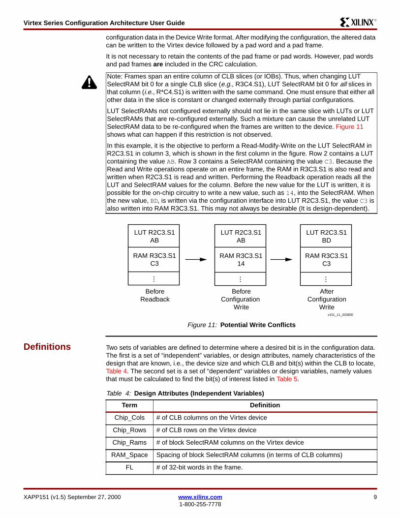
Virtex Series Configuration Architecture User GuideR13
configuration data in the Device Write format After modifying the configuration the altered datacan be written to the Virtex device followed by a pad word and a pad frame
It is not necessary to retain the contents of the pad frame or pad words However pad wordsand pad frames are included in the CRC calculation
Definitions Two sets of variables are defined to determine where a desired bit is in the configuration dataThe first is a set of ldquoindependentrdquo variables or design attributes namely characteristics of thedesign that are known ie the device size and which CLB and bit(s) within the CLB to locateTable 4 The second set is a set of ldquodependentrdquo variables or design variables namely valuesthat must be calculated to find the bit(s) of interest listed in Table 5
Note Frames span an entire column of CLB slices (or IOBs) Thus when changing LUTSelectRAM bit 0 for a single CLB slice (eg R3C4S1) LUT SelectRAM bit 0 for all slices inthat column (ie RC4S1) is written with the same command One must ensure that either allother data in the slice is constant or changed externally through partial configurations
LUT SelectRAMs not configured externally should not lie in the same slice with LUTs or LUTSelectRAMs that are re-configured externally Such a mixture can cause the unrelated LUTSelectRAM data to be re-configured when the frames are written to the device Figure 11shows what can happen if this restriction is not observed
In this example it is the objective to perform a Read-Modify-Write on the LUT SelectRAM inR2C3S1 in column 3 which is shown in the first column in the figure Row 2 contains a LUTcontaining the value AB Row 3 contains a SelectRAM containing the value C3 Because theRead and Write operations operate on an entire frame the RAM in R3C3S1 is also read andwritten when R2C3S1 is read and written Performing the Readback operation reads all theLUT and SelectRAM values for the column Before the new value for the LUT is written it ispossible for the on-chip circuitry to write a new value such as 14 into the SelectRAM Whenthe new value BD is written via the configuration interface into LUT R2C3S1 the value C3 isalso written into RAM R3C3S1 This may not always be desirable (It is design-dependent)
Figure 11 Potential Write Conflicts
x151_11_020800
LUT R2C3S113AB13
RAM R3C3S113C313
Before13Readback
13
LUT R2C3S113AB13
RAM R3C3S1131413
Before13Configuration 13
Write
13
LUT R2C3S113BD13
RAM R3C3S113C313
After13Configuration13
Write
13
Table 4 Design Attributes (Independent Variables)
Term Definition
Chip_Cols of CLB columns on the Virtex device
Chip_Rows of CLB rows on the Virtex device
Chip_Rams of block SelectRAM columns on the Virtex device
RAM_Space Spacing of block SelectRAM columns (in terms of CLB columns)
FL of 32-bit words in the frame
XAPP151 (v15) September 27 2000 wwwxilinxcom 91-800-255-7778
Virtex Series Configuration Architecture User GuideR13
RW 1 for Read 0 for Write
CLB_Col Column number of the desired CLB
CLB_Row Row number of the desired CLB
Slice 0 or 1
FG 0 for the F-LUT 1 for the G-LUT
lut_bit The desired bit from the given LUT Bits in the LUT are indexed from 0 to 15
XY 0 for the X Flip-Flop 1 for the Y Flip-Flop
RAM_Col Column number of the desired block SelectRAM
RAM_Row Row number of the desired block SelectRAM
ram_bit The desired bit from the given block SelectRAM Bits are indexed from 0 to4095
Table 5 Design Variables (Dependent Variables)
Term Definition
MJA Frame Major Address
MNA Frame Minor Address
fm_st_wd The index of the word within a full configuration segment that correspondsto the starting word of the desired frame A full configuration segment isdefined as the following 1) for CLBIOB all CLB IOB and RAMinterconnect frames beginning at MJA=0 MNA=0 and 2) for blockSelectRAM all RAM content frames for the given RAM column Words arenumbered starting at 0
fm_wd The index of the 32-bit word within a frame that contains the desired bitWords in a frame are numbered starting at 0
fm_wd_bit_idx The bit index of the desired bit within frame word fm_wd Words areindexed in ldquobig-endianrdquo style with bit 31 on the left and bit 0 on the right
fm_bit_idx Bit index within a frame of the desired bit Numbered starting with 0 as theleft-most (first) bit Bit numbering within a frame continues across all thewords in the frame
Table 6 Functions used in Equations
Functions Definition
floor(x) The largest integer not larger than x Eg floor(31) = 3 because the nextlargest integer 4 is larger than 31 floor(3)=3
ceiling(x) The smallest integer greater than or equal to x For example ceiling(32) = 4because 4 is greater than 32 and 3 is not ceiling (4) = 4
The modulus operation 5 2 = 1 5 3 = 2 5 5 = 0
Table 4 Design Attributes (Independent Variables) (Continued)
Term Definition
10 wwwxilinxcom XAPP151 (v15) September 27 20001-800-255-7778
Virtex Series Configuration Architecture User GuideR13
CLB LUTSelectRAMDependentVariables
Table 7 shows equations for the LUT SelectRAM ldquoDependent Variablesrdquo that were defined inTable 5
Virtex-E CLB LUT SelectRAM Dependent VariablesThe additional block SelectRAM columns in Virtex-E devices require an adjustment to the MJAThe following equations calculate the adjustment necessary for each of the affected dependentvariables For each variable calculate the base value based upon the Virtex equations onlyand then add the resulting Virtex adjustment
The left and right sides of the device are treated differently
LUT SelectRAM ExamplesSee ldquoExamplesrdquo on page 27 for several examples of reading and evaluating configuration dataThe examples illustrate how to make use of these equations to find the desired data in abitstream
Table 7 Virtex Equations for LUT SelectRAM Dependent Variables
Term Definition
MJA if (CLB_Col le Chip_Cols2)then Chip_Cols ndash CLB_Col times 2 + 2else 2 times CLB_Col ndash Chip_Cols ndash 1
MNA lut_bit + 32 ndash Slice times (2 times lut_bit + 17)
fm_bit_idx 3 + 18 times CLB_Row ndash FG + RW times 32
fm_st_wd FL times (8 + (MJA ndash1) times 48 + MNA) + RW times FL
fm_wd floor(fm_bit_idx32)
fm_wd_bit_idx 31 + 32 times fm_wd ndash fm_bit_idx
Notes
bull Do NOT input the final results back into the original Virtex equations (eg do not useMJAfinal value to calculate fm_st_wd)
bull MJAfinal = MJA + MJA_adj
bull fm_st_wdfinal = fm_st_wd + fm_st_wd_adj
Table 8 CLB Location
CLB Location CLB Column
Left CLB_Col le Chip_Cols2
Right CLB_Col gt Chip_Cols2
Table 9 Virtex-E Families Adjustments for LUT SelectRAM Dependent Variables
Term Definition
MJA_adj Left RAM_Bound = (Chip_Rams2 - 1) x RAM_SpaceMJA_adj = 2 x ceiling((RAM_Bound - CLB_Col + 1) RAM_Space)
Right
RAM_Bound = Chip_Cols - (Chip_Rams2 - 1) x RAM_Space + 1MJA_adj = 2 x ceiling((CLB_Col - RAM_Bound + 1) RAM_Space)
fm_st_wd_adj FL times (27 x MJA_adj)
XAPP151 (v15) September 27 2000 wwwxilinxcom 111-800-255-7778
Virtex Series Configuration Architecture User GuideR13
CLB Flip-FlopDependentVariables
Equations for the CLB flip-flops can be found in Table 10 Their locations are calculatedsimilarly to the LUT SelectRAM locations Equations for the CLB FF Dependent Variables aredefined in Table 5
Virtex-E CLB Flip-Flop Dependent VariablesApply the adjustments given in Table 8 and Table 9
IOB DependentVariables
Each IOB contains four values that can be captured into special registers These values are
bull I mdash the input flip-flop
bull O mdash the output flip-flop
bull T mdash the flip-flop for the tri-state control
bull P mdash the value of the IO pad
These values are captured by utilizing the CAPTURE_VIRTEX symbol in your design TheLibraries Guide has more details on the use of this symbol The following registers will be readas part of the readback data
Access to the IOB flip-flops is different for the top and bottom IOBs versus the left and rightIOBs
The top and bottom IOBs are part of the CLB column frames There are two IOBs at the top andbottom of each CLB column
The left and right IOBs are in columns by themselves There are three IOBs per CLB row
IOBs are numbered clockwise around the die Pad 1 is located at the left side of the top edgeabove CLB column 1 The equations for where to find IOB flip-flops in the bitstream are basedon the pad number which is the same for a given size device not the package pin name whichvaries from package to package The mapping from package pin names to pad numbers canbe found in EPIC or fpga_editor
Table 11 contains the numeric pad indices for the pads on all four edges of the device in termsof the number of CLB columns and rows on the device
Table 10 Virtex Equations for CLB FF Dependent Variables
Term Definition
MJA if (CLB_Col le Chip_Cols2)then Chip_Cols ndash CLB_Col times 2 + 2else 2 times CLB_Col ndash Chip_Cols ndash 1
MNA Slice times (12 times XY ndash 43) ndash 6 times XY + 45
fm_bit_idx (18 times CLB_Row) + 1 + (32 times RW)
fm_st_wd FL times (8 + (MJA ndash1) times 48 + MNA) + RW times FL
fm_wd floor(fm_bit_idx32)
fm_wd_bit_idx 31 + 32 times fm_wd ndash fm_bit_idx
12 wwwxilinxcom XAPP151 (v15) September 27 20001-800-255-7778
Virtex Series Configuration Architecture User GuideR13
Table 12 shows the equations for the dependent variables for the IOB flip-flops The variable iin this table refers to the index of pad i
Table 11 IOB Pad Indices
PadLocation Pad Index i
Top 1 le i le Chip_Cols times 2
Right Chip_Cols times 2 +1 le i le Chip_Cols times 2 + Chip_Rows times 3
Bottom Chip_Cols times 2 + Chip_Rows times 3 + 1 le i le Chip_Cols times 4 + Chip_Rows times 3
Left Chip_Cols times 4 + Chip_Rows times 3 + 1 le i le Chip_Cols times 4 + Chip_Rows times 6
Table 12 Equations for IOB Dependent Variables
Term Definition
MJA
Topif (i le Chip_Cols)then Chip_Cols ndash ceiling(i2) times 2 + 2else 2 times ceiling (i2) ndash Chip_Cols ndash1
Right Chip_Cols + 1
Bottomif (i gt 3 times (Chip_Cols + Chip_Rows))then 2 times ceiling((i ndash 3 times Chip_Cols ndash 3 times Chip_Rows)2)else Chip_Cols ndash 2 times floor((i ndash 2 times Chip_Cols ndash 3 times Chip_Rows ndash 1)2) ndash 1
Left Chip_Cols + 2
MNA
Top
I ndash 25 times (i2) + 45
O ndash 13 times (i2) + 39
T ndash 5 times (i2) + 35
P ndash 4 times (i2) + 25
Right
I t = (i ndash 2 times Chip_Cols) 3 MNA = 275 times t2 ndash 575 times t + 32
O t = (i ndash 2 times Chip_Cols) 3 MNA = 215 times t2 ndash 515 times t + 38
T t = (i ndash 2 times Chip_Cols) 3 MNA = 175 times t2 ndash 475 times t + 42
P 50
Bottom
I 25 times ((i ndash 2 x Chip_Cols - 3 x Chip_Rows)2) + 20
O 13 times ((i ndash 2 x Chip_Cols - 3 x Chip_Rows)2) + 26
T 5 times ((i ndash 2 x Chip_Cols - 3 x Chip_Rows)2) + 30
P 4 times ((i ndash 2 x Chip_Cols - 3 x Chip_Rows)2) + 21
Left
I t = (i ndash 4 x Chip_Cols - 3 x Chip_Rows)3 MNA = 175 times t2 ndash 475 times t + 45
O t = (i ndash 4 x Chip_Cols - 3 x Chip_Rows)3 MNA = 235 times t2 ndash 535 times t + 39
T t = (i ndash 4 x Chip_Cols - 3 x Chip_Rows)3 MNA = 275 times t2 ndash 575 times t + 35
P 50
XAPP151 (v15) September 27 2000 wwwxilinxcom 131-800-255-7778
Virtex Series Configuration Architecture User GuideR13
Virtex-E IOB Dependent VariablesSimilar to CLB dependent variables only the variables affected by the major address aredifferent in Virtex-E and Virtex-EM devices versus Virtex devices A simple way to account forthe change is to determine the CLB column where the pad resides (only true for top andbottom) Then the adjustment calculated for the CLB column can be applied The conversionto CLB columns is found in Table 13
fm_bit_idx
Top 32 times RW
Right
I O ampT 18 times (1 + floor ((i ndash 2 times Chip_Cols ndash 1)3)) + 32 times RW
Pt = (i ndash 2 times Chip_Cols) 3fm_bit_idx = 18 times (1 + floor ((i ndash 2 times Chip_Cols ndash 1)3)) + 6 times t2 ndash 17 times t + 15 + 32 timesRW
Bottom 18 times (Chip_Rows + 1)+ 32 times RW
Left
I O ampT18 times (Chip_Rows ndash floor((i ndash 4 times Chip_Cols ndash 3 times Chip_Rows ndash 1)3)) + 32 times RW
Pt = (i ndash 4 times Chip_Cols ndash 3 times Chip_Rows)3fm_bit_idx = 18 times (Chip_Rows ndash floor ((i ndash 4 times Chip_Cols ndash 3 times Chip_Rows ndash 1)3))ndash 105 times t2 + 215 times t + 4 + 32 times RW
fm_st_wdif (MJA gt Chip_Cols + 1)then FL times (54 times MJA ndash 46 + MNA ndash 6 times Chip_Cols) + RW times FLelse FL times (8 + (MJA ndash1) times 48 + MNA) + RW times FL
fm_wd floor (fm_bit_idx32)
fm_wd_bit_idx 31 + 32 times fm_wd ndash fm_bit_idx
Table 12 Equations for IOB Dependent Variables (Continued)
Term Definition
Table 13 Pad -gt CLB Column
Term Definition
CLB_ColTop ceiling(i2)
Bottom ceiling((4 x Chip_Cols + 3 x Chip_Rows + 1 - i)2)
Table 14 Virtex-E Families Adjustments for IOB Dependent Variables
Term Definition
MJA_adj
Top use Table 8 and Table 9
Right Chip_Rams
Bottom use Table 8 and Table 9
Left Chip_Rams
fm_st_wd_adj FL times (27 x MJA_adj)
14 wwwxilinxcom XAPP151 (v15) September 27 20001-800-255-7778
Virtex Series Configuration Architecture User GuideR13
BlockSelectRAMDependentVariables
The equations for the block SelectRAM dependent variables are given in Table 15 Therelationship of a particular memory cell index in the context of a given configuration is describedin XAPP130 ldquoUsing the Vir tex Bloc k SelectRAM+ Resour cerdquo
Virtex-E Block SelectRAM Dependent VariablesThe RAM major address numbering scheme changed slightly such that the lowest MJA on theleft side is now 2 instead of 0 As in the case for the CLB equations the adjustments belowshould be applied after the Virtex equations
Table 15 Virtex Equations for Block SelectRAM Dependent Variables
Term Definition
MJAif (RAM_Col lt Chip_Rams2)then 2 x (Chip_Rams2 - 1 - RAM_Col)else 2 x (RAM_Col - Chip_Rams2) + 1
MNA
1 x floor(((ram_bit 64) 64)32) + 2 x floor(((ram_bit 64) 32)16)+ 4 x floor(((ram_bit 64) 16)8) + 8 x floor(((ram_bit 64) 8)4)+ 16 x floor(((ram_bit 64) 4)2) + 32 x floor(((ram_bit 64) 2)1)equivalent to MNA = div64[05] where div64[50] = floor(ram_bit64)
fm_bit_idxobtain value for bitpos from Table 16
fm_bit_idx = 18 + 72 x RAM_Row + bitpos
fm_st_wd FL times MNA + RW times FL
fm_wd floor(fm_bit_idx32)
fm_wd_bit_idx 31 + 32 times fm_wd ndash fm_bit_idx
Table 16 Virtex Block SelectRAM Bit Position Within a Given Block SelectRAM
ram
_bit
6
4
bitp
os
ram
_bit
6
4
bitp
os
ram
_bit
6
4
bitp
os
ram
_bit
6
4
bitp
os
ram
_bit
6
4
bitp
os
ram
_bit
6
4
bitp
os
ram
_bit
6
4
bitp
os
ram
_bit
6
4
bitp
os
0 42 8 45 16 29 24 26 32 43 40 44 48 28 56 27
1 58 9 61 17 13 25 10 33 59 41 60 49 12 57 11
2 41 10 46 18 30 26 25 34 40 42 47 50 31 58 24
3 57 11 62 19 14 27 9 35 56 43 63 51 15 59 8
4 50 12 53 20 21 28 18 36 51 44 52 52 20 60 19
5 49 13 54 21 22 29 17 37 48 45 55 53 23 61 16
6 66 14 69 22 5 30 2 38 67 46 68 54 4 62 3
7 65 15 70 23 6 31 1 39 64 47 71 55 7 63 0
Table 17 Virtex-E and Virtex-EM Adjustments for Block SelectRAM DependentVariables
Term Definition
MJA_adj if (RAM_Col lt Chip_Rams2) MJA_adj = 2
XAPP151 (v15) September 27 2000 wwwxilinxcom 151-800-255-7778
Virtex Series Configuration Architecture User GuideR13
ConfigurationLogic Basics
Configuration DataConfiguration data is organized as 32-bit words There are two major commands that theconfiguration data can contain Read and Write A configuration command is executed whenthe configuration command is read or written to the appropriate command register
The OP field contains 01 for a Read operation and 10 for a Write operation (See Figure 12)
A command is organized as a packet with a header word and optional data words The headerword is the first word written to the appropriate command register for a read or write operationThe header word contains a type field (001) an operand field a register address field and aword count field The format for the command header is shown in Figure 13 on page 17
The Register Address field defines the target of this command as defined in Table 18 on page17
The header word count field contains an integer between 0 and 2047 and indicates thenumber of words that follow the header Larger word counts (between 2048 and 1048575words) are achieved by setting the header word count to 0 The Extension header word has atype field = 010 an OP field that must match the OP field in the preceding Command Headerword and a 20-bit word count this format is shown Figure 14 on page 17
Configuration FlowVirtex devices are configured by presenting configuration data to the SelectMAP or JTAGinterfaces in a specific sequence
For Initial Configuration
1 Issue one or more pad words (SelectMAP only)
2 Issue Sync word (SelectMAP only)
3 Reset CRC
4 Set FLR
5 Set COR
6 Set MASK
7 Set CTL (Set PERSIST if you want to keep SelectMAP active after this configuration)
8 Issue a SWITCH (switch CCLK frequency) command to the CMD register This isnecessary only in Master Serial configuration mode
Reading Configuration
These commands can be issued to read a full configuration or for a partial configuration afterthe device has been completely configured
1 Issue a Sync word (SelectMAP only) if the previous configuration command was aborted
2 Set the FAR to the starting address
3 Issue a RCFG (read configuration) command to the CMD register
4 Write the number of words to be read to the FDRO register
5 Flush the command pipeline with a pad word
6 Read data frames
OP CODERead 01Write 10
Figure 12 OP Field Code
16 wwwxilinxcom XAPP151 (v15) September 27 20001-800-255-7778
Virtex Series Configuration Architecture User GuideR13
Writing Configuration
These commands can be issued either as part of an initial configuration or for a partialconfiguration after the device has been configured
1 Issue a Sync word (SelectMAP only) if the previous configuration command was aborted
2 If the frames being written can cause contention then assert the GHIGH_B signal
3 Set the FAR to the starting address
4 Issue a WCFG (write configuration) command to the CMD register
5 Write the number of words to be written to the FDRI register
6 Write data frames
7 If the GHIGH_B signal was asserted de-assert it by writing the LFRM (Last Frame)command to the CMD register and write one pad frame
ConfigurationRegisters
Configuration logic is accessed and controlled via a collection of 32-bit registers called theconfiguration registers (see Table 18) Registers are described in the following sections
Type OP Register Address RSV Word Count31 30 29 28 27 26 25 24 23 22 21 20 19 18 17 16 15 14 13 12 11 10 9 8 7 6 5 4 3 2 1 00 0 1 x x 0 0 0 0 0 0 0 0 0 0 x x x x 0 0 x x x x x x x x x x x
Notes1 Locations within fields containing a zero or one must have these values An X in a bit field indicates that the value is variable and must
be set2 Heavy vertical lines are used to separate fields Light vertical lines separate nibbles in the word
Figure 13 Command Header Format
Type OP Word Count31 30 29 28 27 26 25 24 23 22 21 20 19 18 17 16 15 14 13 12 11 10 9 8 7 6 5 4 3 2 1 00 1 0 x x 0 0 0 0 0 0 0 x x x x x x x x x x x x x x x x x x x x
Notes1 Locations within fields containing a zero or one must have these values An X in a bit field indicates that the value is variable and must
be set2 Heavy vertical lines are used to separate fields Light vertical lines separate nibbles in the word
Figure 14 Large Block Count Header Extension Format
Table 18 Configuration Register Addresses
Register Name Mnemonic RW Binary Address
CRC CRC RW 0000
Frame Address FAR RW 0001
Frame Data Input FDRI W 0010
Frame Data Output FDRO R 0011
Command CMD RW 0100
Control CTL RW 0101
Control Mask MASK RW 0110
Status STAT R 0111
Legacy Output LOUT W 1000
XAPP151 (v15) September 27 2000 wwwxilinxcom 171-800-255-7778
Virtex Series Configuration Architecture User GuideR13
Command Register (CMD)The content of the Command Register (CMD) is interpreted by the configuration state machineConfiguration commands control the operation of the configuration state machine the FrameData Register (FDR) and some of the global signals The command in the Command Registeris executed each time the FAR is loaded with a new value The effect of each command isdefined in Table 19
Configuration Option COR RW 1001
Reserved mdash mdash 1010
Frame Length FLR RW 1011
Reserved mdash mdash 1100
Reserved mdash mdash 1101
Reserved mdash mdash 1110
Reserved mdash mdash 1111
Table 18 Configuration Register Addresses (Continued)
Register Name Mnemonic RW Binary Address
Table 19 Configuration Commands
Cmd Code Description
Rsvd 0000 Reserved
WCFG 0001Write Configuration Data mdash Used prior to writing configuration data to the FDRI It takes theinternal configuration state machine through a sequence of states that control the shifting of the FDRand the writing of the configuration memory (See Frame Data Input Register (FDRI) on page 24)
Rsvd 0010 Reserved
LFRM 0011Last Frame mdash This command is loaded prior to writing the last (pad) data frame if the GHIGH_Bsignal was asserted This command is not necessary if the GHIGH_B signal was not asserted Thisallows overlap of the last frame write with the release of the GHIGH_B signal
RCFG 0100Read Configuration Data mdash Used prior to reading frame data from the FDRO Similar to the WCFGcommand in its effect on the FDR (see Frame Data Output Register (FDRO) on page 24)
START 0101Begin Startup Sequence mdash Starts the startup sequence This command is also used to start ashutdown sequence prior to partial re-configuration The Startup Sequence begins with the nextsuccessful CRC check (see Cyclic Redundancy Check (CRC) on page 22)
RCAP 0110Reset Capture mdash Used when performing capture in single-shot mode This command must be usedto reset the capture signal if single-shot capture has been selected
RCRC 0111 Reset CRC mdash Used to reset CRC register (see Cyclic Redundancy Check (CRC) on page 22)
AGHIGH 1000Assert GHIGH_B Signal mdash Used prior to re-configuration to prevent contention while writing newconfiguration data All CLB outputs and signals are forced to a one
SWITCH 1001Switch CCLK Frequency mdash Used to change (increase) the frequency of the Master CCLK Thenew frequency is specified in Table 21
Rsvd 1010 Reserved
Rsvd 1011 Reserved
Rsvd 1100 Reserved
18 wwwxilinxcom XAPP151 (v15) September 27 20001-800-255-7778
Virtex Series Configuration Architecture User GuideR13
Configuration Option Register (COR)The Configuration Option Register (COR) is used to select configuration options that areillustrated in Figure 15 and defined in Table 20 Entries in this table are further explained in thefollowing tables
Rsvd 1101 Reserved
Rsvd 1110 Reserved
Rsvd 1111 Reserved
Table 19 Configuration Commands (Continued)
Cmd Code Description
DO
NE
_PIP
E
DR
IVE
_DO
NE
SIN
GLE
OS
CF
SE
L
SS
CLK
SR
C
LOC
K_W
AIT
SH
UT
DO
WN
DO
NE
_CY
CLE
LCK
_CY
CLE
GT
S_C
YC
LE
GW
E_C
YC
LE
GS
R_C
YC
LE
31 30 29 28 27 26 25 24 23 22 21 20 19 18 17 16 15 14 13 12 11 10 9 8 7 6 5 4 3 2 1 00 x x x x x x x x x x x x x x x x x x x x x x x x x x x x x x x
Notes1 Locations within fields containing a zero or one must have these values An X in a bit field indicates that the value is variable and must
be set2 Heavy vertical lines are used to separate fields Light vertical lines separate nibbles in the word
Figure 15 COR (Configuration of Option Register) Fields
XAPP151 (v15) September 27 2000 wwwxilinxcom 191-800-255-7778
Virtex Series Configuration Architecture User GuideR13
Table 21 shows the allowed values for the OSCFSEL field of the COR Setting OSCFSEL toone of these values will set the Master CCLK frequency to the specified value
Table 20 Configuration Option Register Fields
Field Bit Indices DescriptionBitgenDefault
DONE_PIPE 30
0 No pipeline stage for DONEIN
1 Add pipeline stage to DONEINFPGA waits on DONE that is delayed by one (1) cycle of the StartupClkrather than the pin itself Use this option when StartupClk is running at highspeeds
0
DRIVE_DONE 290 DONE pin is open drain
1 DONE pin is actively driven high0
SINGLE 28 Readback capture is one-shot 0
OSCFSEL 2722 Select CCLK frequency in Master Serial configuration mode 2
SSCLKSRC 2120
Startup sequence clock source00 Cclk01 UserClk1x JTAGClk
0
LOCK_WAIT 1916
4-bit mask indicating which DLL lock signals to wait for during LCK cycleThe 4 bits (from MSB to LSB) correspond to DLLs TL=3 TR=2 BL=1BR=0 (top-left top-right etc) In Virtex-E devices where there are 8 DLLseach mask bit applies to the 2 DLLs in that quadrant of the device Thedefault is not to wait for any DLL lock signals
0
SHUTDOWN 15
Indicate whether doing a startup or shutdown sequence
0 Startup
1 Shutdown sequence
0
DONE_CYCLE 1412 Startup phase in which DONE pin is released 3
LCK_CYCLE 119 Stall in this startup phase until DLL locks are asserted 7
GTS_CYCLE 86 Startup phase in which IOs switch from tri-state to user design 4
GWE_CYCLE 53 Startup phase in which the global write-enable is asserted 5
GSR_CYCLE 20 Startup phase in which the global setreset is negated 5
Table 21 OSCFSEL-Specified Master CCLK Frequencies)
CCLK(MHz) OSCFSEL
CCLK(MHz) OSCFSEL
CCLK(MHz) OSCFSEL
43 000010 13 001010 41 100111
54 010001 15 001101 45 110011
69 000100 20 010111 51 101010
81 000101 26 011010 55 110100
20 wwwxilinxcom XAPP151 (v15) September 27 20001-800-255-7778
Virtex Series Configuration Architecture User GuideR13
Table 22 shows the values of the DONE_CYCLE LCK_CYCLE GTS_CYCLE GWE_CYCLEand GSR_CYCLE fields in COR This table shows the step in the start-up sequence when eachof these signals becomes active
Control Register (CTL)The Control Register (CTL) fields are illustrated in Figure 16 on page 21 and defined inTable 23
92 000110 30 011101 60 101101
100 000111 34 110010 mdash mdash
Notes1 These values are accurate to +45 ndash 30
Table 22 COR Startup Cycle Fields
FieldValue
DONE_CYCLE(DONE Active)
GTS_CYCLE(GTS_CFGInactive)
GSR_CYCLE(GSR Inactive)
GWE_CYCLE(GWE Active) LCK_CYCLE
000 1 1 1 1 0
001 2 2 2 2 1
010 3 3 3 3 2
011 4 (default) 4 4 4 3
100 5 5 (default) 5 5 4
101 6 6 6 (default) 6 (default) 5
110 mdash DoneIndagger DoneIndagger DoneIndagger 6
111 Keep State Keep State Keep State Keep State Donrsquot Wait(default)
Notes1 dagger DONE if DonePipe = No else the delayed version of DONE
Table 21 OSCFSEL-Specified Master CCLK Frequencies) (Continued)
CCLK(MHz) OSCFSEL
CCLK(MHz) OSCFSEL
CCLK(MHz) OSCFSEL
SB
ITS
PE
RS
IST
GT
S_U
SR
_B
31 30 29 28 27 26 25 24 23 22 21 20 19 18 17 16 15 14 13 12 11 10 9 8 7 6 5 4 3 2 1 00 0 0 0 0 0 0 0 0 0 0 0 0 0 0 0 0 0 0 0 0 0 0 x x x 0 0 0 0 0 x
Notes1 Locations within fields containing a zero or one must have these values An X in a bit field indicates that the value is variable and must
be set2 Heavy vertical lines are used to separate fields Light vertical lines separate nibbles in the word
Figure 16 Control Register Fields
XAPP151 (v15) September 27 2000 wwwxilinxcom 211-800-255-7778
Virtex Series Configuration Architecture User GuideR13
Cyclic Redundancy Check (CRC)A data input error checking mechanism is provided through the Cyclic Redundancy Check(CRC) register When data is written to any configuration register (except LOUT) a 16-bit CRCvalue is calculated using both the register data and the address This value is saved in the CRCregister At the end of any series of writes a pre-calculated CRC block-check value may bewritten to the CRC register If the resulting value is non-zero an error is indicated TheCRC_ERROR bit is accessible through the status register If a CRC error is detectedconfiguration logic is put in the ERROR mode The following section is an algorithm forcomputing CRC
CRC Algorithm Initialization bcc = 0skip_pad = truemore_words = true Check for write operation do
w = next_wordif (w[3127] == rsquo00101rsquo)
A Read OP Donrsquot use in CRCwc = w[100]if (wc == 0)
w = next_wordwc = w[190]
while (wc-- gt 0)
w = next_word
elsif (w[3127] == rsquo00110rsquo)
A Write OP Use in CRC addr = w[1613]if (addr Π0124569DB)
wc = w[100]if (wc == 0)
wc is in next word w = next_wordwc = w[190]
while (wc-- gt 0)
w = next_wordsw[350] = addr wordfor (i=0 ilt36 i++)
Table 23 Control Register Bits
NameBit
Indices Description
SBITS 87 Security level0 ReadWrite OK (default)1 Readback disabled23 Readback disabled Writing disabled except CRCregister
PERSIST 6 Configuration interface remains after configuration0 No (default)1 Yes
GTS_USR_B 0 Active-low global tristate IOs Turn off pull-ups ifGTS_CFG_B is also asserted
22 wwwxilinxcom XAPP151 (v15) September 27 20001-800-255-7778
Virtex Series Configuration Architecture User GuideR13
x16 = bcc[15] XOR sw[i]x15 = bcc[14] XOR x16x2 = bcc[1] XOR x16bcc[150] =
x15bcc[132]x2bcc[0]x16 Note the bit order crc[150] = bcc[015]
else
Pad word - ignore
while (more_words)
Frame Address Register (FAR)The Frame Address Register (FAR) holds the address of the current frame The address isdivided into three parts the block type the major address and the minor address The blocktype field indicates whether the CLB or block RAM address space is used The command in thecommand register is executed each time the FAR is loaded with a new value
The major address selects the CLB or RAM column the minor address selects the frame withinthe column The minor address is incremented each time a full data frame is read from orwritten to the frame data register If the last frame within the CLB column is selected when theincrement occurs the major address is incremented and the minor address is reset to zerootherwise the minor address is incremented However the block RAM major address is notincremented automatically
See Figure 18 for the definitions of valid values for the block type field The FAR field definitionsare shown in Figure 19
Figure 17 CRC Calculation Register
Note the Block RAM Major Address is not incremented automatically To address a differentBlock RAM Content column the FAR must be loaded with the new Major Address
Type CodesCLB 00RAM 01
Figure 18 Block Type Codes
x151_17_021100
15141312111098765432
1013
01234526272829303101
Address 32-bit Data Word
CRC Calculation Register
CRC Data Input Register
CRC Register [310]
DATA_IN
SHIFT
23
16-bit CRC13150
0000 0000 0000 0000133116
1313
XAPP151 (v15) September 27 2000 wwwxilinxcom 231-800-255-7778
Virtex Series Configuration Architecture User GuideR13
Frame Data Input Register (FDRI)The Frame Data Input Register (FDRI) is used to load configuration frame data into a Virtexdevice
The Frame Data Register (FDR) is a shift register into which data is loaded prior to transfer tothe configuration memory Configuration data is written to the Virtex device by loading thecommand register with the WCFG command and then loading the FDR with at least two framesof 32-bit words
The write operation is pipelined such that the first frame of data is written to the configurationmemory while the second frame is being shifted in The last frame (the pad frame) is alwaysdummy data which is not actually written to the configuration memory Each frame write mustinclude enough 32 bit data words to load the frame fully There is one pad word at the end ofeach frame which is required for the pipelining hardware
Frame Data Output Register (FDRO)The Frame Data Output Register (FDRO) is for reading configuration data or captured datafrom the Virtex device a process called readback Readback is performed by loading thecommand register with the RCFG command and then addressing the FDRO with a readcommand
Frame Length Register (FLR)Near the beginning of the configuration bitstream the Frame Length Register (FLR) is writtenwith the length of a frame as measured in 32-bit words This length count is used to providesequencing information for the configuration read and write operations Note that the FLR mustbe written before any FDR operation works It is not necessary to set the FLR more than onceIf the number of bits in a frame is not evenly divisible by 32 the length count of the frame mustbe rounded up to the next highest integer The values for the FLR for all the current Virtexseries devices are given in Table 24
BlockType
Major Address(Column Address)
Minor Address(Frame Address)
31 30 29 28 27 26 25 24 23 22 21 20 19 18 17 16 15 14 13 12 11 10 9 8 7 6 5 4 3 2 1 00 0 0 0 0 x x x x x x x x x x x x x x x x x x 0 0 0 0 0 0 0 0 0
Notes1 Locations within fields containing a zero or one must have these values An X in a bit field indicates that the value is variable and must
be set2 Heavy vertical lines are used to separate fields Light vertical lines separate nibbles in the word
Figure 19 Frame Address Fields (FAR)
Note The FLR contains a value that is one less than the number of words that are read fromor written to a given frame This is because the extra word needed for pipelining is not counted
Table 24 Frame Length Register Value
Device Row times Col Frame Length Words per Frame FLR Value
XCV50E 16 times 24 384 12 11
XCV100E 20 times 30 448 14 13
XCV150 24 times 36 512 16 15
XCV200E 28 times 42 576 18 17
XCV300E 32 times 48 672 21 20
24 wwwxilinxcom XAPP151 (v15) September 27 20001-800-255-7778
Virtex Series Configuration Architecture User GuideR13
Legacy Output Register (LOUT)The Legacy Output Register (LOUT) is used for daisy chaining the configuration bitstream toother Xilinx devices Data written to the LOUT is serialized and appears on the DOUT pin
Mask Register (MASK)The Mask Register (MASK) is a mask register for writes to the CTL register A 1 in bit N of themask allows that bit position to be written in the CTL register The default value of the mask isall 0s
Status Register (STAT)The Status Register (STAT) is loaded with current values of several control or status signalsThe register can be read via the re-configuration block or via JTAG The fields in the Statusregister are illustrated in Figure 20 The values of the signals given in Table 25 on page 26 canbe read from the status register
XCV400E 40 times 60 800 25 24
XCV405E 40 times 60 800 25 24
XCV600E 48 times 72 960 30 29
XCV800 56 times 84 1088 34 33
XCV812E 56 times 84 1088 34 33
XCV1000E 64 times 96 1248 39 38
XCV1600E 72 times 108 1376 43 42
XCV2000E 80 times 120 1536 48 47
XCV2600E 92 times 138 1728 54 53
XCV3200E 104 times 156 1952 61 60
Table 24 Frame Length Register Value (Continued)
Device Row times Col Frame Length Words per Frame FLR Value
DO
NE
INIT
MO
DE
GH
IGH
_B
GS
R_B
GW
E_B
GT
S_C
FG
IN_E
RR
OR
LOC
K
CR
C_E
RR
OR
31 30 29 28 27 26 25 24 23 22 21 20 19 18 17 16 15 14 13 12 11 10 9 8 7 6 5 4 3 2 1 00 0 0 0 0 0 0 0 0 0 0 0 0 0 0 0 0 x x x x x x x x x x x x x x x
Notes1 An X in a bit field indicates that the value is variable2 Heavy vertical lines are used to separate fields Light vertical lines separate nibbles in the word
Figure 20 Status Register Fields
XAPP151 (v15) September 27 2000 wwwxilinxcom 251-800-255-7778
Virtex Series Configuration Architecture User GuideR13
ConfigurationInterface
There are two configuration interfaces to the Virtex devices mdash the bit-serial Boundary Scaninterface and the 8-bit byte-serial SelectMAP interface Conceptually XCV50 configurationdata appears as in Figure 21
Frames and words within frames are written in the same order in both configuration interfacesstarting with Frame 0 word 0 (the left-most in the picture) followed by word 1 etc Bits withineach word are written from left to right (MSB first) in the bit-serial configuration interfaces
Within the SelectMAP interface data is written a byte at a time A sample word is shown inFigure 22 The top row indicates the device pin names The bottom row indicates the bit indiceswithin a configuration word Byte 0 loads first followed by byte 1 et cetera The MSB of eachbyte (ie bits 31 23 15 and 7) is loaded on pin D0 The LSB of each byte (ie bits 24 16 8and 0) is loaded on pin D7
PartialReconfigurationof CLBs
Partial reconfiguration can be performed with and without shutting down the device Ifcontention occurs it is advised to go through a shutdown sequence prior to loadingconfiguration frames When shutting down the DONE pin will go active and pull low If this is notdesireable the DONE pin can be prevented from going low by selecting the DONE_CYCLE toKeep State (111) Similarly to prevent GSR from becoming active and reseting the currentstate the GSR_CYCLE can be set to Keep State When not shutting down changes occurframe by frame but is completely done by the end of the Last Frame packet (see Example 1)
Table 25 Status Register Bits
Name Bit Indices Description
DONE 14 Input from DONE pin
INIT 13 Value of INIT
MODE 1210 Value of M2 M1 M0 mode pins
GHIGH_B 9 0 = GHIGH_B asserted
GSR_B 8 0 = all flip-flops are ResetSet
GWE_B 7 1 = flip-flops and block RAM are write disabled
GTS_CFG 6 0 = IOs are tri-stated
IN_ERROR 5 Legacy input error
LOCK 41 Output from DLL lock signals 1 = DLL is locked
CRC_ERROR 0 Indicates that a CRC error has occurred
Data Frame 0 (11 words) Pad Word
hellip
Data Frame n (11 words) Pad WordPad Frame (12 words)
Figure 21 XCV50 Frame Padding for Reads
Figure 22 SelectMAP Byte and Bit Ordering
x151_22_021100
D0 D1 D2 D3 D4 D5 D6 D7 D0 D1 D2 D3 D4 D5 D6 D7 D0 D1 D2 D3 D4 D5 D6 D7 D0 D1 D2 D3 D4 D5 D6 D7
Byte 0 Byte 1 Byte 2 Byte 313
26 wwwxilinxcom XAPP151 (v15) September 27 20001-800-255-7778
Virtex Series Configuration Architecture User GuideR13
The DONE pin will not change in this case Figure 23 illustrates a typical shutdownreconfiguration in the CLB address space and restart sequence
Examples Several examples of reading and evaluating configuration data are provided to illustrate thefollowing
Figure 23 Typical Shutdown Reconfiguration in the CLB Address Spaceand Restart Sequence
FFFF FFFF Dummy WordAA99 5566 Sync Word Does not realign an already synchronized SelectMap port3001 2001 COR0080 FF2F Shutdown bit set optionally set bit 29 DRIVE_DONE
Alternately COR may be read bit 15 set and written back3000 8001 CMD0000 0005 Start Shutdown3000 8001 CMD0000 0007 Reset CRC0000 00000000 0000 Clock shutdown sequence0000 00000000 00003000 8001 CMD0000 0008 Assert GHIGH3000 8001 CMD0000 0001 Write Configuration3000 2001 FAR0--- ---- Block Type CLB (00) MajorMinor Address3000 4--- FDRI + Word Count if count is lt1024 Otherwise use TypeII Header
Write FRAME DATAIf CLB Frames are not written to non-consecutive addresses repeat FAR word followedby new MajorMinor Address followed by FDRI + Word Count and then Frame Data
3000 0001 Write CRC---- ---- CRC3000 8001 CMD0000 0003 LFRM3000 4--- FDRI + Word Count
Write PAD FRAME
3001 2001 COR0080 3F2D Default COR Options
Alternately COR may be read bit 15 cleared and written back3000 8001 CMD0000 0005 Begin Startup3000 0001 Write CRC---- ---- CRC
0000 00000000 0000 4 Dummy Words0000 00000000 0000
Example 1 Read and Write Semaphores in an XCV100 at CLB R1 C1 Slice 0 on page 28Example 2 Reading the Complete Configuration from an XCV50 on page 33
XAPP151 (v15) September 27 2000 wwwxilinxcom 271-800-255-7778
Virtex Series Configuration Architecture User GuideR13
Example 1 Read and Write Semaphores in an XCV100 at CLB R1 C1Slice 0Semaphores are a useful communication mechanism documented in XAPP 153 ldquoStatus andControl Semaphore Registers using Partial Reconfigurationrdquo Figure 24 shows an abstractionof a microprocessor writing control information to an FPGA and reading status informationOne convention for implementing semaphores in Virtex devices is to use two bits of a 16-bitdual-port RAM as illustrated in Figure 25 This occupies one CLB slice with the F-LUTimplementing the control semaphore and the status semaphore implemented in the G-LUTAddress 15 of the G-LUT is used for on-chip writes to the semaphore and address 14 of the F-LUT is used for on-chip reads Conversely the off-chip microprocessor is reading the G-LUT[15] and writing F-LUT[14]
Example 3 Read the Slice 0 G-LUT from CLB R1 C1 from the Complete Configuration of anXCV50 on page 34Example 4 Read the Slice 1 F-LUT from CLB R19 C16 from an XCV100 on page 36Example 5 Read All Bits in Slice 0 G-LUTs from CLB C2 and XCV50 on page 39Example 6 Read Block SelectRAM index 387 of RAM R2 C0 from an XCV100E on page 41
Figure 24 Semaphore Abstraction
x151_ 23_021400
Status13
Control13
MicroProcessor FPGA13
Semaphores13
28 wwwxilinxcom XAPP151 (v15) September 27 20001-800-255-7778
Virtex Series Configuration Architecture User GuideR13
Using a Semaphore Abstraction dual-port RAM ensures that the LUT SelectRAMs are placedin the CLB in a predictable manner When writing data to one or more LUT SelectRAMs or flip-flops on the device all bits in the frame must have valid configuration information This isassured by altering valid configurations from bitstream files or from frames read from a properlyconfigured Virtex device The latter approach is used in this example
Figure 25 Semaphore ReadWrite Implementation
Frame 47
15
14
47 46
47 46
x151_ 24_021100
Select Map
Frame 46
DING
F
13
D2D3D4 5D6 7D0D1 D D
1
111
0
111
Chip Interface
G F
13
XAPP151 (v15) September 27 2000 wwwxilinxcom 291-800-255-7778
Virtex Series Configuration Architecture User GuideR13
Attributes for this design are summarized in Table 26
From the equations in Table 7 on page 11 the values shown in Table 27 can be calculated
From off-chip for reading the G-LUT[15] bit read one frame (MNA=47) For writing the F-LUT[14] bit we show how to read then write one frame (MNA=46) as opposed to modifyingdata from a bitstream file (both are valid methods) The frames on the XCV100 contain 13 32-bit words and one pad word Remember that fm_st_wd is calculated assuming the entireconfiguration has been read However only the pad frame and then frames 46 and 47 fromMajor Address 30 are being read The desired bit is in Frame 1 word 1 which is word 15
The commands for reading both frames (and the pad frame) are given in Figure 26
Table 26 Design Attributes for Example 1
Attribute
G-LUT [15] F-LUT [14]
Read Read Write
Chip_Rows 20
Chip_Cols 30
FL 14
CLB_Row 1
CLB_Col 1
Slice 0
FG 1 0
lut_bit 15 14
RW 1 1 0
Table 27 Semaphore Example Variables Equations and Values
Variable Equation
Value(s)
G-LUT[15] F-LUT[14]
Read Read Write
MJA 1 le 302 rArr 30 ndash 1 times 2 + 2 30
MNA lut_bit + 32ndash 0 times () 47 46
fm_bit_idx 3 + 18 times 1 ndash FG + RW times 32 52 53 21
fm_st_wd 14 times (8 + (30 ndash 1) times 48+ 4647) +RW times (14 +1)= 14 times (1400 + 4647) + 14 times RW= 19600 + 14 times 4647 + 14 times RW
20272 20258 20244
fm_wd floor (2032) 1 1 0
fm_wd_bit_idx 31 + 32 times 110 ndash 525321 11 10 10
30 wwwxilinxcom XAPP151 (v15) September 27 20001-800-255-7778
Virtex Series Configuration Architecture User GuideR13
The 42 words read are shown in Figure 27 F-LUT[14] is in the second frame (frame=1word=1) at bit 10 The value read is a 1 but because the LUT bits are inverted the logic valueis zero G-LUT[15] is in word one of the third data frame (frame=2 word=1) at bit 11The valueread is a 1 which is a logic zero
InstructionData
Hex 31 30 29 28 27 26 25 24 23 22 21 20 19 18 17 16 15 14 13 12 11 10 9 8 7 6 5 4 3 2 1 0
Sync Word AA99 5566 1 0 1 0 1 0 1 0 1 0 0 1 1 0 0 1 0 1 0 1 0 1 0 1 0 1 1 0 0 1 1 0
Write next (1) word to FAR 3000 2001 0 0 1 1 0 0 0 0 0 0 0 0 0 0 0 0 0 0 1 0 0 0 0 0 0 0 0 0 0 0 0 1
CLB MJA=30 MNA=46 003C 5800 0 0 0 0 0 0 0 0 0 0 1 1 1 1 0 0 0 1 0 1 1 1 0 0 0 0 0 0 0 0 0 0
Write next word to CMD 3000 8001 0 0 1 1 0 0 0 0 0 0 0 0 0 0 0 0 1 0 0 0 0 0 0 0 0 0 0 0 0 0 0 1
Register value for RCFG 0000 0004 0 0 0 0 0 0 0 0 0 0 0 0 0 0 0 0 0 0 0 0 0 0 0 0 0 0 0 0 0 1 0 0
Read from FDRO 2800 602A 0 0 1 0 1 0 0 0 0 0 0 0 0 0 0 0 0 1 1 0 0 0 0 0 0 0 1 0 1 0 1 0
Flush pipe 0000 0000 0 0 0 0 0 0 0 0 0 0 0 0 0 0 0 0 0 0 0 0 0 0 0 0 0 0 0 0 0 0 0 0
(read 42 words)
Notes1 Binary data is grouped in two ways for ease of interpretation Thin vertical lines separate nibble boundaries Heavy vertical lines
separate field boundaries
Figure 26 Commands to Read Two Data Frames
XAPP151 (v15) September 27 2000 wwwxilinxcom 311-800-255-7778
Virtex Series Configuration Architecture User GuideR13
To write to the F-LUT semaphore start with the second data frame (frame=1) that was justread Words 1 - 13 of that frame will become words 0 - 12 of the frame to be written Word 13of this new frame is a pad word and can have any value (typically 0 is chosen) In this newframe set bit 11 of word 0 (zero) to the desired value of the semaphore A pad frame mustfollow the data frame The commands from Figure 28 write these two frames into the device atthe proper location
Frame Word 31 30 29 28 27 26 25 24 23 22 21 20 19 18 17 16 15 14 13 12 11 10 9 8 7 6 5 4 3 2 1 0
0
0 1 1 1 1 1 1 1 1 1 1 1 1 1 1 1 1 1 1 1 1 1 1 1 1 1 1 1 1 1 1 1 1
1 1 1 1 1 1 1 1 1 1 1 1 1 1 1 1 1 1 1 1 1 1 1 1 1 1 1 1 1 1 1 1 1
2 1 1 1 1 1 1 1 1 1 1 1 1 1 1 1 1 1 1 1 1 1 1 1 1 1 1 1 1 1 1 1 1
3 1 1 1 1 1 1 1 1 1 1 1 1 1 1 1 1 1 1 1 1 1 1 1 1 1 1 1 1 1 1 1 1
4 1 1 1 1 1 1 1 1 1 1 1 1 1 1 1 1 1 1 1 1 1 1 1 1 1 1 1 1 1 1 1 1
5 1 1 1 1 1 1 1 1 1 1 1 1 1 1 1 1 1 1 1 1 1 1 1 1 1 1 1 1 1 1 1 1
6 1 1 1 1 1 1 1 1 1 1 1 1 1 1 1 1 1 1 1 1 1 1 1 1 1 1 1 1 1 1 1 1
7 1 1 1 1 1 1 1 1 1 1 1 1 1 1 1 1 1 1 1 1 1 1 1 1 1 1 1 1 1 1 1 1
8 1 1 1 1 1 1 1 1 1 1 1 1 1 1 1 1 1 1 1 1 1 1 1 1 1 1 1 1 1 1 1 1
9 1 1 1 1 1 1 1 1 1 1 1 1 1 1 1 1 1 1 1 1 1 1 1 1 1 1 1 1 1 1 1 1
10 1 1 1 1 1 1 1 1 1 1 1 1 1 1 1 1 1 1 1 1 1 1 1 1 1 1 1 1 1 1 1 1
11 1 1 1 1 1 1 1 1 1 1 1 1 1 1 1 1 1 1 1 1 1 1 1 1 1 1 1 1 1 1 1 1
12 1 1 1 1 1 1 1 1 1 1 1 1 1 1 1 1 1 1 1 1 1 1 1 1 1 1 1 1 1 1 1 1
13 1 1 1 1 1 1 1 1 1 1 1 1 1 1 1 1 1 1 1 1 1 1 1 1 1 1 1 1 1 1 1 1
1
0 0 0 0 0 0 0 0 0 0 0 0 0 0 0 0 0 0 0 0 0 0 0 0 0 0 0 0 0 0 0 0 0
1 1 0 0 0 0 0 0 0 0 0 0 0 1 0 0 0 0 1 1 0 1 1 0 0 0 0 0 0 0 0 0 0 F[14]
2 1 1 1 1 1 0 1 1 0 0 0 0 1 1 1 1 0 0 1 1 1 1 1 0 1 1 0 0 0 0 0 0
3 0 0 0 0 1 1 1 1 1 0 1 1 0 0 0 0 0 0 0 0 0 0 1 1 1 1 1 0 1 1 0 0
4 0 0 0 0 0 0 0 0 1 1 1 1 0 0 0 0 0 0 0 0 0 0 0 0 0 0 1 1 1 1 1 0
5 1 1 0 0 1 1 0 0 0 0 0 0 1 1 0 0 1 0 1 1 0 0 0 0 0 0 0 0 0 0 1 1
6 1 1 1 0 1 1 0 0 0 0 0 0 1 1 1 0 1 1 1 0 1 0 1 1 0 0 0 0 0 0 0 0
7 0 0 1 1 1 1 1 0 1 1 0 0 0 0 1 1 0 0 0 0 1 1 1 1 1 0 1 1 0 0 0 0
8 0 0 0 0 0 0 1 1 1 1 1 0 0 0 0 0 0 0 0 0 0 0 0 0 1 1 1 1 1 0 1 1
9 0 0 0 0 0 0 0 0 0 0 1 1 0 0 0 0 1 1 0 0 0 0 0 0 0 0 0 0 1 1 1 1
10 1 0 1 1 0 0 0 0 0 0 0 0 1 0 1 1 1 1 1 0 1 1 0 0 0 0 0 0 0 0 0 0
11 1 1 1 1 1 0 1 1 0 0 0 0 1 1 1 1 0 0 1 1 1 1 1 0 1 1 0 0 0 0 0 0
12 0 0 0 0 1 1 0 1 1 0 1 1 0 0 0 0 0 0 0 0 0 0 1 1 1 1 1 0 0 0 0 0
13 0 0 0 0 0 0 1 1 0 1 0 1 0 0 0 0 0 0 0 0 0 0 0 0 0 0 0 0 0 0 0 0
2
0 0 0 0 0 0 0 0 0 0 0 0 0 0 0 0 0 0 0 0 0 0 0 0 0 0 0 0 0 0 0 0 0
1 1 0 1 0 0 0 0 0 0 0 0 1 1 0 1 0 1 1 1 0 1 1 0 0 0 0 0 0 0 0 0 0 G[15]
2 1 1 1 1 1 1 1 1 0 0 0 0 1 1 1 1 0 0 1 1 1 1 1 1 1 1 0 0 0 0 0 0
3 0 0 0 0 1 1 1 1 1 1 1 1 0 0 0 0 0 0 0 0 0 0 1 0 1 1 1 1 1 1 0 0
4 0 0 0 0 0 0 0 0 1 1 1 1 0 0 0 0 0 0 0 0 0 0 0 0 0 0 1 1 1 1 1 1
5 1 1 0 0 0 0 0 0 0 0 0 0 1 1 0 0 1 1 1 1 0 0 1 0 0 0 0 0 0 0 1 1
6 1 1 1 1 1 1 0 0 0 0 0 0 1 1 1 1 1 1 1 1 1 1 1 1 0 0 0 0 0 0 0 0
7 0 0 1 1 1 1 1 1 1 1 0 0 0 0 1 1 0 0 0 0 1 1 1 1 1 1 1 1 0 0 0 0
8 0 0 0 0 0 0 1 1 1 1 1 1 0 0 0 0 0 0 0 0 0 0 0 0 1 1 1 1 1 1 1 1
9 0 0 0 0 0 0 0 0 0 0 1 1 0 0 0 0 1 1 0 0 0 0 0 0 0 0 0 0 1 1 1 1
10 1 1 1 1 0 0 0 0 0 0 0 0 1 1 1 1 1 1 1 1 1 1 0 0 0 0 0 0 0 0 0 0
11 1 1 1 1 1 1 1 1 0 0 0 0 1 1 1 1 0 0 1 1 1 1 1 1 1 1 0 0 0 0 0 0
12 0 0 0 0 1 1 0 1 1 1 1 1 0 0 0 0 0 0 0 0 0 0 1 1 1 1 1 0 1 0 0 0
13 0 0 0 0 0 1 1 0 0 1 1 1 0 0 0 0 0 0 0 0 0 0 0 0 0 0 0 0 0 0 0 0
Figure 27 Three Frames Containing the Semaphores
32 wwwxilinxcom XAPP151 (v15) September 27 20001-800-255-7778
Virtex Series Configuration Architecture User GuideR13
Example 2 Reading the Complete Configuration from an XCV50Steps
1 If flip-flop values are needed clock the on-chip signal CAPTURE to capture flip-flopvalues See the Xilinx Libraries Guide for use of the CAPTURE_VIRTEX cell
2 Write the starting frame address (CLB MJA=0 MNA=0) into the FAR
3 Write the RCFG command to the CMD register
4 Address the FDRO register with a READ operation and word count equal to the number of32-bit words in the CLB frames plus one pad frame
5 Read the data following the timing diagrams in the SelectMAP interface section
6 Write the address for RAM block 0 to the FAR
7 Address the FDRO register with a read operation and word count equal to the number of32-bit words in the RAM block plus one pad frame
8 Read the data
9 Write the address for RAM block 1 to the FAR
10 Address the FDRO register with a read operation and word count equal to the number of32-bit words in the RAM block plus one pad frame
11 Read the data
When using SelectMAP mode to read data words from the Virtex device de-assert CS de-assert WRITE assert CS then clock the data out When using JTAG load the JTAG IR
InstructionData
Hex 31 30 29 28 27 26 25 24 23 22 21 20 19 18 17 16 15 14 13 12 11 10 9 8 7 6 5 4 3 2 1 0
Sync Word AA995566
1 0 1 0 1 0 1 0 1 0 0 1 1 0 0 1 0 1 0 1 0 1 0 1 0 1 1 0 0 1 1 0
Write next (1) word to FAR 30002001
0 0 1 1 0 0 0 0 0 0 0 0 0 0 0 0 0 0 1 0 0 0 0 0 0 0 0 0 0 0 0 1
MJA=30 MNA=46 003C5C00
0 0 0 0 0 0 0 0 0 0 1 1 1 1 0 0 0 1 0 1 1 1 0 0 0 0 0 0 0 0 0 0
Write next word to CMD 30008001
0 0 1 1 0 0 0 0 0 0 0 0 0 0 0 0 1 0 0 0 0 0 0 0 0 0 0 0 0 0 0 1
Register value for WCFG 00000001
0 0 0 0 0 0 0 0 0 0 0 0 0 0 0 0 0 0 0 0 0 0 0 0 0 0 0 0 0 0 0 1
Write 28 words to FDRI 3000401C
0 0 1 1 0 0 0 0 0 0 0 0 0 0 0 0 0 1 0 0 0 0 0 0 0 0 0 1 1 1 0 0
Data Word 0 A01AEC00
1 0 1 0 0 0 0 0 0 0 0 1 1 0 1 0 1 1 1 0 1 1 0 0 0 0 0 0 0 0 0 0
Data Word 1 FF0F3FC0
1 1 1 1 1 1 1 1 0 0 0 0 1 1 1 1 0 0 1 1 1 1 1 1 1 1 0 0 0 0 0 0
Data Word 2 0FF002FC
0 0 0 0 1 1 1 1 1 1 1 1 0 0 0 0 0 0 0 0 0 0 1 0 1 1 1 1 1 1 0 0
hellip hellip hellip
Data Word 27 00000000
0 0 0 0 0 0 0 0 0 0 0 0 0 0 0 0 0 0 0 0 0 0 0 0 0 0 0 0 0 0 0 0
Notes1 Binary data is grouped in two ways for ease of interpretation Thin vertical lines separate nibble boundaries Heavy
vertical lines separate field boundaries
Figure 28 Commands to Write a Semaphore Value
XAPP151 (v15) September 27 2000 wwwxilinxcom 331-800-255-7778
Virtex Series Configuration Architecture User GuideR13
(instruction register) with the CFG_OUT instruction Then go to the SDR (Shift-DR) state andshift the data out (See Figure 29)
Example 3 Read the Slice 0 G-LUT from CLB R1 C1 from the CompleteConfiguration of an XCV50The commands for reading the bitstream from the Virtex device are given in Example 1 Readand Write Semaphores in an XCV100 at CLB R1 C1 Slice 0 on page 28 Using an XCV50device the independent attributes are show in Table 28
InstructionData
Hex 31 30 29 28 27 26 25 24 23 22 21 20 19 18 17 16 15 14 13 12 11 10 9 8 7 6 5 4 3 2 1 0
Sync Word AA99 5566 1 0 1 0 1 0 1 0 1 0 0 1 1 0 0 1 0 1 0 1 0 1 0 1 0 1 1 0 0 1 1 0
Write next word to FAR 3000 2001 0 0 1 1 0 0 0 0 0 0 0 0 0 0 0 0 0 0 1 0 0 0 0 0 0 0 0 0 0 0 0 1
CLB MJA=0 MNA=0 0000 0000 0 0 0 0 0 0 0 0 0 0 0 0 0 0 0 0 0 0 0 0 0 0 0 0 0 0 0 0 0 0 0 0
Write next word to CMDregister
3000 8001 0 0 1 1 0 0 0 0 0 0 0 0 0 0 0 0 1 0 0 0 0 0 0 0 0 0 0 0 0 0 0 1
Register value for RCFG 0000 0004 0 0 0 0 0 0 0 0 0 0 0 0 0 0 0 0 0 0 0 0 0 0 0 0 0 0 0 0 0 1 0 0
Read from FDRO register 2800 6000 0 0 1 0 1 0 0 0 0 0 0 0 0 0 0 0 0 1 1 0 0 0 0 0 0 0 0 0 0 0 0 0
15876 words 4800 3E04 0 1 0 0 1 0 0 0 0 0 0 0 0 0 0 0 0 0 1 1 1 1 1 0 0 0 0 0 0 1 0 0
Flush pipe 0000 0000 0 0 0 0 0 0 0 0 0 0 0 0 0 0 0 0 0 0 0 0 0 0 0 0 0 0 0 0 0 0 0 0
(Read 15876 words)Write to FAR register 3000 2001 0 0 1 1 0 0 0 0 0 0 0 0 0 0 0 0 0 0 1 0 0 0 0 0 0 0 0 0 0 0 0 1
RAM MJA=0 MNA=0 0200 0000 0 0 0 0 0 0 1 0 0 0 0 0 0 0 0 0 0 0 0 0 0 0 0 0 0 0 0 0 0 0 0 0
Read 780 words fromFDRO reg
2800 630C 0 0 1 0 1 0 0 0 0 0 0 0 0 0 0 0 0 1 1 0 0 0 1 1 0 0 0 0 1 1 0 0
Flush pipe 0000 0000 0 0 0 0 0 0 0 0 0 0 0 0 0 0 0 0 0 0 0 0 0 0 0 0 0 0 0 0 0 0 0 0
(Read 780 words)Write to FAR register 3000 2001 0 0 1 1 0 0 0 0 0 0 0 0 0 0 0 0 0 0 1 0 0 0 0 0 0 0 0 0 0 0 0 1
RAM MJA=1 MNA=0 0202 0000 0 0 0 0 0 0 1 0 0 0 0 0 0 0 1 0 0 0 0 0 0 0 0 0 0 0 0 0 0 0 0 0
Read 780 words fromFDRO reg
2800 630C 0 0 1 0 1 0 0 0 0 0 0 0 0 0 0 0 0 1 1 0 0 0 1 1 0 0 0 0 1 1 0 0
Flush pipe 0000 0000 0 0 0 0 0 0 0 0 0 0 0 0 0 0 0 0 0 0 0 0 0 0 0 0 0 0 0 0 0 0 0 0
(Read 780 words)
Figure 29 Example 2 - Read Complete Configuration for XCV50
Table 28 XCV50 Independent Attributes
Independent Attributes Values
Chip_Rows 16
Chip_Cols 24
FL 12
CLB_Row 1
CLB_Col 1
FG 1
Slice 0
RW 1
34 wwwxilinxcom XAPP151 (v15) September 27 20001-800-255-7778
Virtex Series Configuration Architecture User GuideR13
From the equations given earlier in Table 7 calculating the range of values for fm_st_wdindicates that the word 13740 of the configuration is the starting word of the 12-word (FL=12)frame containing bit 0 of the G-LUT in Slice 0 of CLB R1C1 (Table 29)
The configuration bits for the given frame are as follows G-LUT[0] is in fm_wd=0 at bit 11
All 16 LUT SelectRAM bits are in the following words at the same bit index 11
Table 29 Variables Equations and Values for Slice 0 G-LUT
Variables Equations Values
MJA 1 le 242 rArr 24 ndash 1times 2 + 2 24
MNA 0 times (hellip) + lut_bit + 32 0 321 332 343 35
4 365 376 387 39
8 409 41
10 4211 43
12 4413 4514 4615 47
fm_bit_idx 3 + 18 times 1 ndash1 + RW times 32 52
fm_st_wd 12 times (8+ (24 ndash1) times 48 + [3247]) +1 x 12= 12 times (1112 + [3247]) +12= 13356 + 12 times 3247]
1374013920
fm_wd floor(5232) 1
fm_wd_bit_idx 31 + 32 ndash 52 11
BitstreamWord
Frame 32-bit Word FrameWord31 30 29 28 27 26 25 24 23 22 21 20 19 18 17 16 15 14 13 12 11 10 9 8 7 6 5 4 3 2 1 0
13740 0 0 0 0 0 0 0 0 0 0 0 0 0 0 0 0 0 0 0 0 0 0 0 0 0 0 0 0 0 0 0 0 013741 0 0 1 0 1 0 0 0 0 0 0 0 0 1 0 1 0 1 0 0 1 1 1 0 0 0 0 0 0 0 0 0 113742 1 0 1 1 0 0 1 1 0 0 0 0 0 0 0 0 0 0 1 0 1 1 0 0 1 1 0 0 0 0 0 0 213743 0 0 0 0 1 0 1 1 0 0 1 1 0 0 0 0 0 0 0 0 0 0 1 0 1 1 0 0 1 1 0 0 313744 0 0 0 0 0 0 0 0 1 0 1 1 0 0 1 1 0 0 0 0 0 0 0 0 0 0 1 0 1 1 0 0 413745 1 1 0 0 0 0 0 0 0 0 0 0 1 0 1 1 0 0 1 1 0 0 0 0 0 0 0 0 0 0 1 0 513746 1 1 0 0 1 1 0 0 0 0 0 0 0 0 0 0 1 0 1 1 0 0 1 1 0 0 0 0 0 0 0 0 613747 0 0 1 0 1 1 0 0 1 1 0 0 0 0 0 0 0 0 0 0 1 0 1 1 0 0 1 1 0 0 0 0 713748 0 0 0 0 0 0 1 0 1 1 0 0 1 1 0 0 0 0 0 0 0 0 0 0 1 0 1 1 0 0 1 1 813749 0 0 0 0 0 0 0 0 0 0 1 0 1 1 0 0 1 1 0 0 0 0 0 0 0 0 0 0 1 0 1 1 913750 0 0 1 1 0 0 0 0 0 0 0 0 0 0 1 0 1 1 0 0 1 0 1 0 0 0 0 0 0 0 0 0 1013751 0 1 0 1 0 0 0 0 0 0 0 0 0 0 0 0 0 0 0 0 0 0 0 0 0 0 0 0 0 0 0 0 11
Figure 30 Configuration Bits for Slice 0 CLB R1C1 G-LUT [0]
XAPP151 (v15) September 27 2000 wwwxilinxcom 351-800-255-7778
Virtex Series Configuration Architecture User GuideR13
The 16 bits are LUT[150]=0111111111111111 The LUT SelectRAM bits are inverted from theirlogic values The ldquologicalrdquo contents are LUT[150]=1000000000000000 Thus this G-LUTimplements a 4-input AND function
Example 4 Read the Slice 1 F-LUT from CLB R19 C16 from an XCV100Commands for reading the bitstream from the Virtex device are given in Figure 32 Use thefollowing independent attributes to find the given F-LUT
From the equations in Table 7 on page 11 calculating fm_st_wd indicates the starting wordwith respect to a configuration that starts at MJA=0 MNA=0 Because the frames we are
BitstreamWord
Frame 32-bit Word
LUT Bit31 30 29 28 27 26 25 24 23 22 21 20 19 18 17 16 15 14 13 12 11 10 9 8 7 6 5 4 3 2 1 0
13741 0 0 1 0 1 0 0 0 0 0 0 0 0 1 0 1 0 1 0 0 1 1 1 0 0 0 0 0 0 0 0 0 0
13753 1 0 1 0 0 0 0 0 0 0 0 0 0 0 0 1 0 0 0 1 1 1 0 0 0 0 0 0 0 0 0 0 1
13765 1 0 1 0 1 0 0 0 0 0 0 0 1 0 0 0 0 0 0 1 1 1 1 0 0 0 0 0 0 0 0 0 2
13777 0 0 0 0 1 0 0 0 0 0 0 1 1 1 0 1 1 0 1 0 1 1 0 0 0 0 0 0 0 0 0 0 3
13789 0 1 0 0 0 0 0 0 0 0 0 0 0 1 0 1 1 1 1 1 1 1 1 0 0 0 0 0 0 0 0 0 4
13801 1 0 1 0 1 0 0 0 0 0 0 1 0 0 0 1 1 0 0 1 1 1 0 0 0 0 0 0 0 0 0 0 5
13813 0 0 0 1 0 0 0 0 0 0 0 0 0 0 0 0 1 0 0 1 1 1 0 0 0 0 0 0 0 0 0 0 6
13825 0 1 1 0 1 0 0 0 0 0 0 1 0 1 0 0 1 1 0 0 1 1 0 0 0 0 0 0 0 0 0 0 7
13837 1 0 1 1 1 0 0 0 0 0 0 1 0 1 0 1 1 0 0 0 1 1 0 0 0 0 0 0 0 0 0 0 8
13849 1 0 0 0 0 0 0 0 0 0 0 0 0 0 0 0 1 1 1 0 1 1 0 0 0 0 0 0 0 0 0 0 9
13861 1 0 0 0 0 0 0 0 0 0 0 1 0 0 0 0 1 1 1 1 1 1 1 0 0 0 0 0 0 0 0 0 10
13873 1 0 0 0 0 0 0 1 0 0 0 0 0 1 0 0 0 1 1 0 1 1 0 0 0 1 0 0 0 0 0 0 11
13885 1 0 0 0 0 0 0 0 0 0 0 0 0 1 0 1 0 0 1 0 1 1 0 0 0 0 0 0 0 0 0 0 12
13897 0 0 0 0 1 0 0 0 0 0 0 0 0 1 0 0 0 0 0 0 1 1 0 0 0 0 0 0 0 0 0 0 13
13909 1 0 0 0 0 0 0 0 0 0 0 0 1 1 0 1 0 1 1 0 1 1 0 0 0 0 0 0 0 0 0 0 14
13921 1 0 1 0 0 0 0 0 0 0 0 1 1 1 0 1 1 1 1 1 0 1 0 0 0 0 0 0 0 0 0 0 15
Figure 31 Location of all 16 LUT SelectRAM Bits
Table 30 Virtex Bitstream Command Attributes
Independent Attributes Values
Chip_Rows 20
Chip_Cols 30
FL 14
CLB_Row 19
CLB_Col 16
FG 0
Slice 1
RW 1
36 wwwxilinxcom XAPP151 (v15) September 27 20001-800-255-7778
Virtex Series Configuration Architecture User GuideR13
interested in start at MJA=1 MNA=0 which is fm_st_wd = 126 so the first 126 words are notneeded (0ndash125) Therefore to find the given Slice 1 F-LUT see Table 31
Sixteen frames need to be read one for each bit in the LUT SelectRAM The bits in LUTSelectRAMs in Slice 1 occur in the opposite order that they do for Slice 0 LUT SelectRAMs
Frames are read sequentially with ascending addresses If read in LUT bit order LUT[0]LUT[1] hellip LUT[15] These are stored in descending addresses which require 16 separateread operations each reading one data frame and one pad frame However if read inascending address order LUT[15] LUT[14] hellip LUT[0] all 16 data frames are read with asingle read operation This requires only one pad frame for all 16 frames Thus it takes lesstime to read ascending frames starting at MJA=1 MNA=0 and finishing with frame MJA=1MNA=15 The frames in the XCV100 contain 14 32-bit words and a single pad wordCommands for reading only the F-LUT data are given in Figure 32
Table 31 Variables Equations and Values for Slice 1 F-LUT
Variables Equations Values
MJA 16 gt 302 rArr 2times16 ndash 30 ndash1 1
MNA lut_bit + 32 ndash Slice times (2 times lut_bit +17)= [015] + 32 ndash (2 times [015] + 17)= 15 ndash [015]
0 151 142 133 12
4 115 106 97 8
8 79 6
10 511 4
12 313 214 115 0
fm_bit_idx 3 + 18 times 19 ndash 0+ 32 377
fm_st_wd 14 times (8 + (1ndash 1) times 48 + [150]) +1 times 14= 14 times (8 + [150]) +14= 126 + 14 times [150]
= 336126
fm_wd floor(37732) 11
fm_wd_bit_idx 31 + 32 times 11 ndash 377 6
XAPP151 (v15) September 27 2000 wwwxilinxcom 371-800-255-7778
Virtex Series Configuration Architecture User GuideR13
The 377th bit of each frame is the bit in the F-LUT This LUT SelectRAM bit is in the framersquosword index 11 bit index 6
The configuration bits for the given frame in Figure 33 are as follows LUT Bit 15 is in MJA=1MNA=0 fm_wd=11 at bit 6
LUT bit 0 is in MJA=1 MNA=15 fm_wd=11 at bit 6
InstructionData
Hex 31 30 29 28 27 26 25 24 23 22 21 20 19 18 17 16 15 14 13 12 11 10 9 8 7 6 5 4 3 2 1 0
Sync Word AA99 5566 1 0 1 0 1 0 1 0 1 0 0 1 1 0 0 1 0 1 0 1 0 1 0 1 0 1 1 0 0 1 1 0
Write next (1) word to FAR 3000 2001 0 0 1 1 0 0 0 0 0 0 0 0 0 0 0 0 0 0 1 0 0 0 0 0 0 0 0 0 0 0 0 1
CLB MJA = 1 MNA = 0 0002 0000 0 0 0 0 0 0 0 0 0 0 0 0 0 0 1 0 0 0 0 0 0 0 0 0 0 0 0 0 0 0 0 0
Write next word to CMD 3000 8001 0 0 1 1 0 0 0 0 0 0 0 0 0 0 0 0 1 0 0 0 0 0 0 0 0 0 0 0 0 0 0 1
Register value for RCFG 0000 0004 0 0 0 0 0 0 0 0 0 0 0 0 0 0 0 0 0 0 0 0 0 0 0 0 0 0 0 0 0 1 0 0
Read from FDRO 2800 60EE 0 0 1 0 1 0 0 0 0 0 0 0 0 0 0 0 0 1 1 0 0 0 0 0 1 1 1 0 1 1 1 0
Flush pipe 0000 0000 0 0 0 0 0 0 0 0 0 0 0 0 0 0 0 0 0 0 0 0 0 0 0 0 0 0 0 0 0 0 0 0
(Read 238 words)
Figure 32 Commands to read Slice 1 F-LUT
Frame WordFrame 32-bit Word
31 30 29 28 27 26 25 24 23 22 21 20 19 18 17 16 15 14 13 12 11 10 9 8 7 6 5 4 3 2 1 0
0 0 0 0 0 0 0 0 0 0 0 0 0 0 0 0 0 0 0 0 0 0 0 0 0 0 0 0 0 0 0 0 0
1 1 1 0 0 0 0 0 0 0 0 0 0 0 1 0 1 1 1 1 1 1 1 0 0 0 0 0 0 0 0 0 0
2 1 1 1 1 1 1 1 1 0 0 0 0 0 0 0 0 0 0 1 1 1 1 1 1 1 1 0 0 0 0 0 0
3 0 0 0 0 1 1 1 1 1 1 1 1 0 0 0 0 0 0 0 0 0 0 1 1 1 1 1 1 1 1 0 0
4 0 0 0 0 0 0 0 0 1 1 1 1 1 1 1 1 0 0 0 0 0 0 0 0 0 0 1 1 1 1 1 1
5 1 1 0 0 0 0 0 0 0 0 0 0 1 1 1 1 1 1 1 1 0 0 0 0 0 0 0 0 0 0 1 1
6 1 1 1 1 1 1 0 0 0 0 0 0 0 0 0 0 1 1 1 1 1 1 1 1 0 0 0 0 0 0 0 0
7 0 0 1 1 1 1 1 1 1 1 0 0 0 0 0 0 0 0 0 0 1 1 1 1 1 1 1 1 0 0 0 0
8 0 0 0 0 0 0 1 1 1 1 1 1 1 1 0 0 0 0 0 0 0 0 0 0 1 1 1 1 1 1 1 1
9 0 0 0 0 0 0 0 0 0 0 1 1 1 1 1 1 1 1 0 0 0 0 0 0 0 0 0 0 1 1 1 1
10 1 1 1 1 0 0 0 0 0 0 0 0 0 0 1 1 1 1 1 1 1 1 0 0 0 0 0 0 0 0 0 0
11 1 1 1 1 1 1 1 1 0 0 0 0 0 0 0 0 0 0 1 1 1 1 1 1 1 0 0 0 0 0 0 0
12 0 0 0 0 1 1 1 1 1 1 1 1 0 0 0 0 0 0 0 0 0 0 1 1 1 1 1 1 0 0 0 0
13 0 0 0 0 0 0 0 0 0 1 1 1 0 0 0 0 0 0 0 0 0 0 1 1 1 1 1 1 0 0 0 0
Figure 33 Frame Containing F-LUT[15]
Bit streamWord
Frame 32-bit WordFmWd31 30 29 28 27 26 25 24 23 22 21 20 19 18 17 16 15 14 13 12 11 10 9 8 7 6 5 4 3 2 1 0
336 0 0 0 0 0 0 0 0 0 0 0 0 0 0 0 0 0 0 0 0 0 0 0 0 0 0 0 0 0 0 0 0 0337 0 1 0 0 1 0 0 0 0 0 0 1 0 1 0 0 1 1 0 0 1 1 0 0 0 0 0 0 0 0 0 0 1338 1 0 1 1 0 0 1 1 0 0 0 0 0 0 0 0 0 0 1 0 1 1 0 0 1 1 0 0 0 0 0 0 2339 0 0 0 0 1 0 1 1 0 0 1 1 0 0 0 0 0 0 0 0 0 0 1 0 1 1 0 0 1 1 0 0 3340 0 0 0 0 0 0 0 0 1 0 1 1 0 0 1 1 0 0 0 0 0 0 0 0 0 0 1 0 1 1 0 0 4341 1 1 0 0 0 0 0 0 0 0 0 0 1 0 1 1 0 0 1 1 0 0 0 0 0 0 0 0 0 0 1 0 5342 1 1 0 0 1 1 0 0 0 0 0 0 0 0 0 0 1 0 1 1 0 0 1 1 0 0 0 0 0 0 0 0 6343 0 0 1 0 1 1 0 0 1 1 0 0 0 0 0 0 0 0 0 0 1 0 1 1 0 0 1 1 0 0 0 0 7
Figure 34 Frame Containing F-LUT [0]
38 wwwxilinxcom XAPP151 (v15) September 27 20001-800-255-7778
Virtex Series Configuration Architecture User GuideR13
For the sake of brevity here are the sixteen 11th words in the order they appear in thebitstream
The bits are LUT[150]=0111111111111111 The LUT SelectRAM bits are inverted from thelogic sense The logical contents are LUT[150]=1000000000000000 Thus this F-LUTimplements a 4-input AND gate
Example 5 Read All Bits in Slice 0 G-LUTs from CLB C2 and XCV50Given the following attributes the necessary values to find the G-LUT data can be computed
344 0 0 0 0 0 0 1 0 1 1 0 0 1 1 0 0 0 0 0 0 0 0 0 0 1 0 1 1 0 0 1 1 8345 0 0 0 0 0 0 0 0 0 0 1 0 1 1 0 0 1 1 0 0 0 0 0 0 0 0 0 0 1 0 1 1 9346 0 0 1 1 0 0 0 0 0 0 0 0 0 0 1 0 1 1 0 0 1 1 0 0 0 0 0 0 0 0 0 0 10347 1 1 1 1 1 0 1 1 0 0 0 0 0 0 0 0 0 0 1 0 1 1 1 0 1 1 0 1 0 0 0 0 11348 0 0 0 0 1 1 1 0 1 0 1 1 0 0 0 0 0 0 0 0 0 0 1 1 1 1 0 1 0 0 0 0 12349 0 0 0 0 0 1 0 0 0 0 1 0 0 0 0 0 0 0 0 0 0 0 0 0 0 0 0 0 0 0 0 0 13
Bit streamWord
Frame 32-bit WordFmWd31 30 29 28 27 26 25 24 23 22 21 20 19 18 17 16 15 14 13 12 11 10 9 8 7 6 5 4 3 2 1 0
Figure 34 Frame Containing F-LUT [0]
BitstreamWord
Frame 32-bit WordLUT Bit31 30 29 28 27 26 25 24 23 22 21 20 19 18 17 16 15 14 13 12 11 10 9 8 7 6 5 4 3 2 1 0
137 1 1 1 1 1 1 1 1 0 0 0 0 0 0 0 0 0 0 1 1 1 1 1 1 1 0 0 0 0 0 0 0 15151 1 0 1 1 1 0 1 1 0 0 0 0 0 0 0 0 0 0 1 0 1 1 1 0 1 1 0 0 0 0 0 0 14165 1 0 1 1 0 0 1 1 0 0 0 0 0 0 0 0 0 0 1 0 1 1 1 0 1 1 0 0 0 0 0 0 13179 1 0 1 1 1 0 1 1 0 0 0 0 0 0 0 0 0 0 1 0 1 1 1 0 1 1 0 0 0 0 0 0 12193 1 1 1 1 1 0 1 1 0 0 0 0 0 0 0 0 0 0 1 1 1 1 1 0 1 1 0 0 0 0 0 0 11207 1 1 1 1 1 1 1 1 0 0 0 0 0 0 0 0 0 0 1 1 1 1 1 1 1 1 1 0 1 0 0 0 10221 1 1 1 1 1 0 1 1 0 0 0 0 0 0 0 0 0 0 1 1 1 1 1 0 1 1 0 0 0 0 0 0 9235 1 0 1 1 1 0 1 1 0 0 0 0 0 0 0 0 0 0 1 0 1 1 1 0 1 1 0 0 0 0 0 0 8249 1 0 1 1 0 0 1 1 0 0 0 0 0 0 0 0 0 0 1 0 1 1 0 0 1 1 0 0 0 0 0 0 7263 1 0 1 1 0 1 1 1 1 0 0 0 0 0 0 0 0 0 1 0 1 1 0 1 1 1 0 0 0 0 0 0 6277 1 1 1 1 0 0 1 1 0 0 0 0 0 0 0 0 0 0 1 1 1 1 0 0 1 1 0 0 0 0 0 0 5291 1 1 1 1 1 1 1 1 0 0 0 0 0 0 0 0 0 0 1 1 1 1 1 1 1 1 0 0 0 0 0 0 4305 1 1 1 1 1 0 1 1 0 0 0 0 0 0 0 0 0 0 1 1 1 1 1 0 1 1 0 0 0 0 0 0 3319 1 0 1 1 0 1 1 1 0 0 0 0 0 0 0 0 0 0 1 0 1 1 0 1 1 1 0 0 0 0 0 0 2333 1 0 1 1 0 0 1 1 0 0 0 0 0 0 0 0 0 0 1 0 1 1 0 0 1 1 0 0 0 0 0 0 1347 1 1 1 1 1 0 1 1 0 0 0 0 0 0 0 0 0 0 1 0 1 1 1 0 1 1 0 1 0 0 0 0 0
Figure 35 Sixteen Words Containing the F-LUT bit
Table 32 All Bits Slice 0 GndashLUTs from CLB C2 and XCV50
Independent Attributes Values
Chip_Rows 16
Chip_Cols 24
FL 12
CLB_Row 116
CLB_Col 2
XAPP151 (v15) September 27 2000 wwwxilinxcom 391-800-255-7778
Virtex Series Configuration Architecture User GuideR13
From the equations in Table 7 the dependent variables can be calculated
Note that fm_bit_idx fm_wd and fm_wd_bit_idx have 16 values one for each row on theXCV50 Figure 37 shows where the data lies in the first frame which contains G[0] for the entirecolumn The process is the same for the other 15 frames The commands for reading the LUTSelectRAM data are given in Figure 36
From the calculation for fm_st_wd Frame 0 would start at word 12588 reading the wholeconfiguration The instructions in Figure 36 start at that word so word 0 (ignoring the 12 wordsin the pad frame) is the same as word 12588 of the entire CLB configuration The 12 words inthe frame are shown in Figure 37
FG 1
Slice 0
lut_bit 015
RW 1
Table 32 All Bits Slice 0 GndashLUTs from CLB C2 and XCV50 (Continued)
Independent Attributes Values
Table 33 Dependent Variables Equations and Values
Variables Equations Values
MJA 2 le 242 rArr 24 ndash 2times 2 + 2 22
MNAlut_bit + 32 ndash Slice times (2 times lut_bit + 17)= lut_bit + 32 ndash 0 times (2 times lut_bit + 17)= [015] + 32
032 436 840 1244
133 537 941 1345
234 638 1042 1456
335 739 1143 1547
fm_bit_idx3 + 18 times CLB_Row ndash 1+ 32 = 34 + 18 times[116]
152 5124 9196 13268
270 6142 10214 14286
388 7160 11232 15304
4106 8178 12250 16322
fm_st_wd12 times (8 + (22 ndash1) times 48 + MNA) + 1 times 12= 12 times (1016 + MNA) + 12= 12204 + 12 times MNA
0 12588 4 12636 8 12684 12 12732
1 12600 5 12648 9 12696 13 12744
2 12612 6 12660 10 12708 14 12756
3 12624 7 12672 11 12720 15 12768
fm_wd floor (fm_bit_idx32)
11 53 96 138
22 64 106 148
32 75 117 159
43 85 127 1610
fm_wd_bit_idx 31 + 32 times fm_wd ndash fm_bit_idx
111 53 927 1319
225 617 109 141
37 7 31 1123 1515
421 813 125 1629
40 wwwxilinxcom XAPP151 (v15) September 27 20001-800-255-7778
Virtex Series Configuration Architecture User GuideR13
The LUT SelectRAM bits have been shaded for ease of identification It can be seen from thecalculation of fm_bit_idx that the LUT SelectRAM bits are in the order 116 For example fromthe above calculations for fm_wd and fm_wd_bit_idx G-LUT[0] in R1C2 is in fm_wd 1fm_wd_bit_idx 11 This bit is the shaded bit in word 1 at bit index 11 Similarly the G-LUT[0] forthe other 15 CLB rows are also shaded in this table
Example 6 Read Block SelectRAM index 387 of RAM R2 C0 from anXCV100ECommands for reading the bitstream from the Virtex device are given in Figure 38 Use thefollowing independent attributes to find the given F-LUT
InstructionData
Hex 31 30 29 28 27 26 25 24 23 22 21 20 19 18 17 16 15 14 13 12 11 10 9 8 7 6 5 4 3 2 1 0
Sync Word AA99 5566 1 0 1 0 1 0 1 0 1 0 0 1 1 0 0 1 0 1 0 1 0 1 0 1 0 1 1 0 0 1 1 0
Write next (1) word to FAR 3000 2001 0 0 1 1 0 0 0 0 0 0 0 0 0 0 0 0 0 0 1 0 0 0 0 0 0 0 0 0 0 0 0 1
CLB MJA=22 MNA=32 002C 4000 0 0 0 0 0 0 0 0 0 0 1 0 1 1 0 0 0 1 0 0 0 0 0 0 0 0 0 0 0 0 0 0
Write next word to CMD 3000 8001 0 0 1 1 0 0 0 0 0 0 0 0 0 0 0 0 1 0 0 0 0 0 0 0 0 0 0 0 0 0 0 1
Register value for RCFG 0000 0004 0 0 0 0 0 0 0 0 0 0 0 0 0 0 0 0 0 0 0 0 0 0 0 0 0 0 0 0 0 1 0 0
Read from FDRO 2800 60CC 0 0 1 0 1 0 0 0 0 0 0 0 0 0 0 0 0 1 1 0 0 0 0 0 1 1 0 0 1 1 0 0
Flush pipe 0000 0000 0 0 0 0 0 0 0 0 0 0 0 0 0 0 0 0 0 0 0 0 0 0 0 0 0 0 0 0 0 0 0 0
(Read 204 words)
Figure 36 Commands to read RC2S0 G-LUT
WordFrame 32-bit Word
CLB Row31 30 29 28 27 26 25 24 23 22 21 20 19 18 17 16 15 14 13 12 11 10 9 8 7 6 5 4 3 2 1 0
0 0 0 0 0 0 0 0 0 0 0 0 0 0 0 0 0 0 0 0 0 0 0 0 0 0 0 0 0 0 0 0 0
1 0 0 0 0 1 0 0 0 0 0 0 0 0 1 0 1 0 1 0 0 1 1 0 0 0 0 0 0 0 0 0 0 12 1 0 1 1 0 0 1 1 0 0 0 0 0 0 0 0 0 0 1 0 1 1 0 0 1 1 0 0 0 0 0 0 2 33 0 0 0 0 1 0 1 1 0 0 1 1 0 0 0 0 0 0 0 0 0 0 1 0 1 1 0 0 1 1 0 0 4 54 0 0 0 0 0 0 0 0 1 0 1 1 0 0 1 1 0 0 0 0 0 0 0 0 0 0 1 0 1 1 0 0 65 1 1 0 0 0 0 0 0 0 0 0 0 1 0 1 1 0 0 1 1 0 0 0 0 0 0 0 0 0 0 1 0 7 86 1 1 0 0 1 1 0 0 0 0 0 0 0 0 0 0 1 0 1 1 0 0 1 1 0 0 0 0 0 0 0 0 9 107 0 0 1 0 1 1 0 0 1 1 0 0 0 0 0 0 0 0 0 0 1 0 1 1 0 0 1 1 0 0 0 0 11 128 0 0 0 0 0 0 1 0 1 1 0 0 1 1 0 0 0 0 0 0 0 0 0 0 1 0 1 1 0 0 1 1 13 149 0 0 0 0 0 0 0 0 0 0 1 0 1 1 0 0 1 1 0 0 0 0 0 0 0 0 0 0 1 0 1 1 15
10 0 0 1 1 0 0 0 0 0 0 0 0 0 0 1 0 1 1 0 0 1 0 1 0 0 0 0 0 0 0 0 0 1611 0 1 0 1 0 0 0 0 0 0 0 0 0 0 0 0 0 0 0 0 0 0 0 0 0 0 0 0 0 0 0 0
Figure 37 Frame for RC2S0 G-LUTs Bit G[0]
Table 34 Virtex Bitstream Command Attributes
Independent Attributes Values
Chip_Rams 4
FL 14
RAM_Row 2
RAM_Col 0
ram_bit 387
RW 1
XAPP151 (v15) September 27 2000 wwwxilinxcom 411-800-255-7778
Virtex Series Configuration Architecture User GuideR13
Since we are attempting to read only one bit location only one frame is necessary to be readWe use the equations of Table 15 Table 16 and Table 17 to determine the dependentvariables
Commands for reading this memory index are given in Figure 38
RAM bit 387 is at fm_wd=6 bit 4
Table 35 Variables Equations and Values for Slice 1 F-LUT
Variables Equations Values
MJA_virtex 0 lt42 rArr 2times(42 -1 -0) 2
MJA_adj 0 lt42 rArr 2 2
MJA MJA_virtex + MJA_adj 4
MNA floor(((38764)64)32)+ 2 x floor(((38764)32)16)+ 4 x floor(((38764)16)8) + 8 x floor(((38764)8)4)+ 16 x floor(((38764)4)2) + 32 x floor(((38764)2)1)
24
fm_bit_idx 3 + 18 times 19 ndash 0 + 32 219
fm_st_wd 14 x 24 + 1 x 14 350
fm_wd floor(21932) 6
fm_wd_bit_idx 31 + 32 times 6 ndash 219 4
InstructionData
Hex 31 30 29 28 27 26 25 24 23 22 21 20 19 18 17 16 15 14 13 12 11 10 9 8 7 6 5 4 3 2 1 0
Sync Word AA99 5566 1 0 1 0 1 0 1 0 1 0 0 1 1 0 0 1 0 1 0 1 0 1 0 1 0 1 1 0 0 1 1 0
Write next (1) word to FAR 3000 2001 0 0 1 1 0 0 0 0 0 0 0 0 0 0 0 0 0 0 1 0 0 0 0 0 0 0 0 0 0 0 0 1
CLB MJA = 4 MNA = 24 0208 3000 0 0 0 0 0 0 1 0 0 0 0 0 1 0 0 0 0 0 1 1 0 0 0 0 0 0 0 0 0 0 0 0
Write next word to CMD 3000 8001 0 0 1 1 0 0 0 0 0 0 0 0 0 0 0 0 1 0 0 0 0 0 0 0 0 0 0 0 0 0 0 1
Register value for RCFG 0000 0004 0 0 0 0 0 0 0 0 0 0 0 0 0 0 0 0 0 0 0 0 0 0 0 0 0 0 0 0 0 1 0 0
Read from FDRO 2800 601C 0 0 1 0 1 0 0 0 0 0 0 0 0 0 0 0 0 1 1 0 0 0 0 0 0 0 0 1 1 1 0 0
Flush pipe 0000 0000 0 0 0 0 0 0 0 0 0 0 0 0 0 0 0 0 0 0 0 0 0 0 0 0 0 0 0 0 0 0 0 0
(Read 28 words)
Figure 38 Commands to read Block SelectRAM index 387
42 wwwxilinxcom XAPP151 (v15) September 27 20001-800-255-7778
Virtex Series Configuration Architecture User GuideR13
Glossary Block SelectRAM Resource
One of several large fully-synchronous dual-port memories in the Virtex FPGAs Each ofthese memories contain 4096 bits The organization of each memory is configurable Theblock SelectRAM resource complements the smaller distributed LUT SelectRAMs
Boundary Scan Interface
One of the configuration interfaces on the Virtex device This is a bit-serial interface TheBoundary Scan interface is also known as the JTAG port Also see the SelectMAP interface
Capture Data
The flip-flop and pad data saved from the logic cells and IO blocks into the bitstream Use theCAPTURE_VIRTEX primitive in your HDL code to specify the trigger and clock for the captureoperation
Configurable Logic Block (CLB)
The functional elements for constructing logic circuits The Virtex CLB is made up of Sliceswhich contain Logic Cells
Configuration Bitstream
Configuration commands optionally with configuration data
Configuration Commands
Instructions for the Virtex device There are two classes of Configuration Command mdash Majorand Minor The Major Commands read and write data to configuration registers in the Virtexdevice The Minor commands instruct the Virtex configuration logic to perform specificfunctions See Command Register (CMD) on page 18
Configuration Data
Bits that directly define the state of programmable logic These are written to a Virtex device ina configuration bitstream and read as Readback Data from a Virtex device
Frame WordFrame 32-bit Word
31 30 29 28 27 26 25 24 23 22 21 20 19 18 17 16 15 14 13 12 11 10 9 8 7 6 5 4 3 2 1 0
0 0 0 0 0 0 0 0 0 0 0 0 0 0 0 0 0 0 0 0 0 0 0 0 0 0 0 0 0 0 0 0 0
1 1 1 0 0 0 0 0 0 0 0 0 0 0 1 0 1 1 1 1 1 1 1 0 0 0 0 0 0 0 0 0 0
2 1 1 1 1 1 1 1 1 0 0 0 0 0 0 0 0 0 0 1 1 1 1 1 1 1 1 0 0 0 0 0 0
3 0 0 0 0 1 1 1 1 1 1 1 1 0 0 0 0 0 0 0 0 0 0 1 1 1 1 1 1 1 1 0 0
4 0 0 0 0 0 0 0 0 1 1 1 1 1 1 1 1 0 0 0 0 0 0 0 0 0 0 1 1 1 1 1 1
5 1 1 0 0 0 0 0 0 0 0 0 0 1 1 1 1 1 1 1 1 0 0 0 0 0 0 0 0 0 0 1 1
6 1 1 1 1 1 1 0 0 0 0 0 0 0 0 0 0 1 1 1 1 1 1 1 1 0 0 0 0 0 0 0 0
7 0 0 1 1 1 1 1 1 1 1 0 0 0 0 0 0 0 0 0 0 1 1 1 1 1 1 1 1 0 0 0 0
8 0 0 0 0 0 0 1 1 1 1 1 1 1 1 0 0 0 0 0 0 0 0 0 0 1 1 1 1 1 1 1 1
9 0 0 0 0 0 0 0 0 0 0 1 1 1 1 1 1 1 1 0 0 0 0 0 0 0 0 0 0 1 1 1 1
10 1 1 1 1 0 0 0 0 0 0 0 0 0 0 1 1 1 1 1 1 1 1 0 0 0 0 0 0 0 0 0 0
11 1 1 1 1 1 1 1 1 0 0 0 0 0 0 0 0 0 0 1 1 1 1 1 1 1 0 0 0 0 0 0 0
12 0 0 0 0 1 1 1 1 1 1 1 1 0 0 0 0 0 0 0 0 0 0 1 1 1 1 1 1 0 0 0 0
13 0 0 0 0 0 0 0 0 0 1 1 1 0 0 0 0 0 0 0 0 0 0 1 1 1 1 1 1 0 0 0 0
Figure 39 Frame MNA=24
XAPP151 (v15) September 27 2000 wwwxilinxcom 431-800-255-7778
Virtex Series Configuration Architecture User GuideR13
Configuration Frame
The configuration bits in a Virtex device are organized in columns A column of CLBs with theIO blocks above and below the CLBs contain 48 frames of configuration bits The smallestnumber of bits that can be read or written through the configuration interfaces is one frame
Configuration Interface
A logical interface on the Virtex device through which configuration commands and data can beread and written A interface consists of one or more physical Device Pins
Configuration Readback
The operation of reading Configuration Data (also known as Readback Data) from a Virtexdevice
Device Pin
One of the electrical connections on the package containing the Virtex device
Frame
See Configuration Frame
Logic Cell (LC)
The basic building block of the Virtex CLB An LC includes a 4-input function generator carrylogic and a storage element
LUT SelectRAMs
Shallow RAM structures implemented in CLB Lookup Tables (LUTs) See also blockSelectRAM section
Pad
Pad bits are extra bits used to make the total number of bits in a frame an integral multiple of32 the number of bits in a configuration word A Pad Word is an extra word used at the end ofa Configuration Frame for pipelining A Pad Frame is an extra Configuration Frame used at thebeginning of a Configuration Readback and at the end of a Configuration Write for pipelining
Readback Data
Configuration data read from a Virtex device The data is organized as Configuration Frames
SelectMAP Interface
One of the configuration interfaces on the Virtex device This is a byte-serial interface The pinsin the SelectMAP interface may be used as user IO after configuration has been completed orremain configured as a configuration interface
Slice
A subdivision of the Virtex CLB There are two vertical slices in a Virtex CLB Each slicecontains two Logic Cells
Sync Word
A 32-bit word with a value that is used to synchronize the configuration logic
44 wwwxilinxcom XAPP151 (v15) September 27 20001-800-255-7778
Virtex Series Configuration Architecture User GuideR13
RevisionHistory
The following table shows the revision history for this document
Date Version Revision
061799 10 Initial Release
072799 11 Updated the following tables Table 5 equation for MNA Table 7equations for MJA amp fm_bit_idx
092099 12 Changes in page 5 Most formulae in Table 7 have been revisedDocumented pad capture value P Corrected bit locations inExamples
022200 13 Updated to include Virtex-E block SelectRAM Correctedfm_bit_idx (Right IOB) equations in Table 12 and fm_st_wddefinition Corrected CRC algorithm Various corrections inExamples Reformatted and edited document and figures
080300 14 Updated to include Virtex-EM devices in Table 3 and Table 24
092700 15 Added Partial Reconfiguration of CLB section and Figure 26
XAPP151 (v15) September 27 2000 wwwxilinxcom 451-800-255-7778
- Summary
- Introduction
-
- CLBs IOBs and Configurations
-
- Configuring Virtex Devices
- Reading Configuration Bits From a Virtex Device
-
- Configuration Columns
- Configuration Addressing
-
- Block Type Major Address Minor Address
-
- Virtex Major Addresses
- Virtex-EM Major Addresses
- Virtex-E Major Addresses
-
- Frames
-
- Frame Sizes
- Frame Organization
- Location of LUT SelectRAM Bits
-
- Configuration Data Operations
-
- Reading Configuration Data
- Writing Configuration Data
- Altering Configuration Data
-
- Definitions
- CLB LUT SelectRAM Dependent Variables
-
- Virtex-E CLB LUT SelectRAM Dependent Variables
- LUT SelectRAM Examples
-
- CLB Flip-Flop Dependent Variables
-
- Virtex-E CLB Flip-Flop Dependent Variables
-
- IOB Dependent Variables
-
- Virtex-E IOB Dependent Variables
-
- Block SelectRAM Dependent Variables
-
- Virtex-E Block SelectRAM Dependent Variables
-
- Configuration Logic Basics
-
- Configuration Data
- Configuration Flow
-
- For Initial Configuration
- Reading Configuration
- Writing Configuration
-
- Configuration Registers
-
- Command Register (CMD)
- Configuration Option Register (COR)
- Control Register (CTL)
- Cyclic Redundancy Check (CRC)
-
- CRC Algorithm
-
- Frame Address Register (FAR)
- Frame Data Input Register (FDRI)
- Frame Data Output Register (FDRO)
- Frame Length Register (FLR)
- Legacy Output Register (LOUT)
- Mask Register (MASK)
- Status Register (STAT)
-
- Configuration Interface
- Partial Reconfiguration of CLBs
- Examples
-
- Example 1 Read and Write Semaphores in an XCV100 at CLB R1 C1 Slice 0
- Example 2 Reading the Complete Configuration from an XCV50
- Example 3 Read the Slice 0 G-LUT from CLB R1 C1 from the Complete Configuration of an XCV50
- Example 4 Read the Slice 1 F-LUT from CLB R19 C16 from an XCV100
- Example 5 Read All Bits in Slice 0 G-LUTs from CLB C2 and XCV50
- Example 6 Read Block SelectRAM index 387 of RAM R2 C0 from an XCV100E
-
- Glossary
-
- Block SelectRAM Resource
- Boundary Scan Interface
- Capture Data
- Configurable Logic Block (CLB)
- Configuration Bitstream
- Configuration Commands
- Configuration Data
- Configuration Frame
- Configuration Interface
- Configuration Readback
- Device Pin
- Frame
- Logic Cell (LC)
- LUT SelectRAMs
- Pad
- Readback Data
- SelectMAP Interface
- Slice
- Sync Word
-
- Revision History
-
Virtex Series Configuration Architecture User GuideR13
CLB Flip-FlopDependentVariables
Equations for the CLB flip-flops can be found in Table 10 Their locations are calculatedsimilarly to the LUT SelectRAM locations Equations for the CLB FF Dependent Variables aredefined in Table 5
Virtex-E CLB Flip-Flop Dependent VariablesApply the adjustments given in Table 8 and Table 9
IOB DependentVariables
Each IOB contains four values that can be captured into special registers These values are
bull I mdash the input flip-flop
bull O mdash the output flip-flop
bull T mdash the flip-flop for the tri-state control
bull P mdash the value of the IO pad
These values are captured by utilizing the CAPTURE_VIRTEX symbol in your design TheLibraries Guide has more details on the use of this symbol The following registers will be readas part of the readback data
Access to the IOB flip-flops is different for the top and bottom IOBs versus the left and rightIOBs
The top and bottom IOBs are part of the CLB column frames There are two IOBs at the top andbottom of each CLB column
The left and right IOBs are in columns by themselves There are three IOBs per CLB row
IOBs are numbered clockwise around the die Pad 1 is located at the left side of the top edgeabove CLB column 1 The equations for where to find IOB flip-flops in the bitstream are basedon the pad number which is the same for a given size device not the package pin name whichvaries from package to package The mapping from package pin names to pad numbers canbe found in EPIC or fpga_editor
Table 11 contains the numeric pad indices for the pads on all four edges of the device in termsof the number of CLB columns and rows on the device
Table 10 Virtex Equations for CLB FF Dependent Variables
Term Definition
MJA if (CLB_Col le Chip_Cols2)then Chip_Cols ndash CLB_Col times 2 + 2else 2 times CLB_Col ndash Chip_Cols ndash 1
MNA Slice times (12 times XY ndash 43) ndash 6 times XY + 45
fm_bit_idx (18 times CLB_Row) + 1 + (32 times RW)
fm_st_wd FL times (8 + (MJA ndash1) times 48 + MNA) + RW times FL
fm_wd floor(fm_bit_idx32)
fm_wd_bit_idx 31 + 32 times fm_wd ndash fm_bit_idx
12 wwwxilinxcom XAPP151 (v15) September 27 20001-800-255-7778
Virtex Series Configuration Architecture User GuideR13
Table 12 shows the equations for the dependent variables for the IOB flip-flops The variable iin this table refers to the index of pad i
Table 11 IOB Pad Indices
PadLocation Pad Index i
Top 1 le i le Chip_Cols times 2
Right Chip_Cols times 2 +1 le i le Chip_Cols times 2 + Chip_Rows times 3
Bottom Chip_Cols times 2 + Chip_Rows times 3 + 1 le i le Chip_Cols times 4 + Chip_Rows times 3
Left Chip_Cols times 4 + Chip_Rows times 3 + 1 le i le Chip_Cols times 4 + Chip_Rows times 6
Table 12 Equations for IOB Dependent Variables
Term Definition
MJA
Topif (i le Chip_Cols)then Chip_Cols ndash ceiling(i2) times 2 + 2else 2 times ceiling (i2) ndash Chip_Cols ndash1
Right Chip_Cols + 1
Bottomif (i gt 3 times (Chip_Cols + Chip_Rows))then 2 times ceiling((i ndash 3 times Chip_Cols ndash 3 times Chip_Rows)2)else Chip_Cols ndash 2 times floor((i ndash 2 times Chip_Cols ndash 3 times Chip_Rows ndash 1)2) ndash 1
Left Chip_Cols + 2
MNA
Top
I ndash 25 times (i2) + 45
O ndash 13 times (i2) + 39
T ndash 5 times (i2) + 35
P ndash 4 times (i2) + 25
Right
I t = (i ndash 2 times Chip_Cols) 3 MNA = 275 times t2 ndash 575 times t + 32
O t = (i ndash 2 times Chip_Cols) 3 MNA = 215 times t2 ndash 515 times t + 38
T t = (i ndash 2 times Chip_Cols) 3 MNA = 175 times t2 ndash 475 times t + 42
P 50
Bottom
I 25 times ((i ndash 2 x Chip_Cols - 3 x Chip_Rows)2) + 20
O 13 times ((i ndash 2 x Chip_Cols - 3 x Chip_Rows)2) + 26
T 5 times ((i ndash 2 x Chip_Cols - 3 x Chip_Rows)2) + 30
P 4 times ((i ndash 2 x Chip_Cols - 3 x Chip_Rows)2) + 21
Left
I t = (i ndash 4 x Chip_Cols - 3 x Chip_Rows)3 MNA = 175 times t2 ndash 475 times t + 45
O t = (i ndash 4 x Chip_Cols - 3 x Chip_Rows)3 MNA = 235 times t2 ndash 535 times t + 39
T t = (i ndash 4 x Chip_Cols - 3 x Chip_Rows)3 MNA = 275 times t2 ndash 575 times t + 35
P 50
XAPP151 (v15) September 27 2000 wwwxilinxcom 131-800-255-7778
Virtex Series Configuration Architecture User GuideR13
Virtex-E IOB Dependent VariablesSimilar to CLB dependent variables only the variables affected by the major address aredifferent in Virtex-E and Virtex-EM devices versus Virtex devices A simple way to account forthe change is to determine the CLB column where the pad resides (only true for top andbottom) Then the adjustment calculated for the CLB column can be applied The conversionto CLB columns is found in Table 13
fm_bit_idx
Top 32 times RW
Right
I O ampT 18 times (1 + floor ((i ndash 2 times Chip_Cols ndash 1)3)) + 32 times RW
Pt = (i ndash 2 times Chip_Cols) 3fm_bit_idx = 18 times (1 + floor ((i ndash 2 times Chip_Cols ndash 1)3)) + 6 times t2 ndash 17 times t + 15 + 32 timesRW
Bottom 18 times (Chip_Rows + 1)+ 32 times RW
Left
I O ampT18 times (Chip_Rows ndash floor((i ndash 4 times Chip_Cols ndash 3 times Chip_Rows ndash 1)3)) + 32 times RW
Pt = (i ndash 4 times Chip_Cols ndash 3 times Chip_Rows)3fm_bit_idx = 18 times (Chip_Rows ndash floor ((i ndash 4 times Chip_Cols ndash 3 times Chip_Rows ndash 1)3))ndash 105 times t2 + 215 times t + 4 + 32 times RW
fm_st_wdif (MJA gt Chip_Cols + 1)then FL times (54 times MJA ndash 46 + MNA ndash 6 times Chip_Cols) + RW times FLelse FL times (8 + (MJA ndash1) times 48 + MNA) + RW times FL
fm_wd floor (fm_bit_idx32)
fm_wd_bit_idx 31 + 32 times fm_wd ndash fm_bit_idx
Table 12 Equations for IOB Dependent Variables (Continued)
Term Definition
Table 13 Pad -gt CLB Column
Term Definition
CLB_ColTop ceiling(i2)
Bottom ceiling((4 x Chip_Cols + 3 x Chip_Rows + 1 - i)2)
Table 14 Virtex-E Families Adjustments for IOB Dependent Variables
Term Definition
MJA_adj
Top use Table 8 and Table 9
Right Chip_Rams
Bottom use Table 8 and Table 9
Left Chip_Rams
fm_st_wd_adj FL times (27 x MJA_adj)
14 wwwxilinxcom XAPP151 (v15) September 27 20001-800-255-7778
Virtex Series Configuration Architecture User GuideR13
BlockSelectRAMDependentVariables
The equations for the block SelectRAM dependent variables are given in Table 15 Therelationship of a particular memory cell index in the context of a given configuration is describedin XAPP130 ldquoUsing the Vir tex Bloc k SelectRAM+ Resour cerdquo
Virtex-E Block SelectRAM Dependent VariablesThe RAM major address numbering scheme changed slightly such that the lowest MJA on theleft side is now 2 instead of 0 As in the case for the CLB equations the adjustments belowshould be applied after the Virtex equations
Table 15 Virtex Equations for Block SelectRAM Dependent Variables
Term Definition
MJAif (RAM_Col lt Chip_Rams2)then 2 x (Chip_Rams2 - 1 - RAM_Col)else 2 x (RAM_Col - Chip_Rams2) + 1
MNA
1 x floor(((ram_bit 64) 64)32) + 2 x floor(((ram_bit 64) 32)16)+ 4 x floor(((ram_bit 64) 16)8) + 8 x floor(((ram_bit 64) 8)4)+ 16 x floor(((ram_bit 64) 4)2) + 32 x floor(((ram_bit 64) 2)1)equivalent to MNA = div64[05] where div64[50] = floor(ram_bit64)
fm_bit_idxobtain value for bitpos from Table 16
fm_bit_idx = 18 + 72 x RAM_Row + bitpos
fm_st_wd FL times MNA + RW times FL
fm_wd floor(fm_bit_idx32)
fm_wd_bit_idx 31 + 32 times fm_wd ndash fm_bit_idx
Table 16 Virtex Block SelectRAM Bit Position Within a Given Block SelectRAM
ram
_bit
6
4
bitp
os
ram
_bit
6
4
bitp
os
ram
_bit
6
4
bitp
os
ram
_bit
6
4
bitp
os
ram
_bit
6
4
bitp
os
ram
_bit
6
4
bitp
os
ram
_bit
6
4
bitp
os
ram
_bit
6
4
bitp
os
0 42 8 45 16 29 24 26 32 43 40 44 48 28 56 27
1 58 9 61 17 13 25 10 33 59 41 60 49 12 57 11
2 41 10 46 18 30 26 25 34 40 42 47 50 31 58 24
3 57 11 62 19 14 27 9 35 56 43 63 51 15 59 8
4 50 12 53 20 21 28 18 36 51 44 52 52 20 60 19
5 49 13 54 21 22 29 17 37 48 45 55 53 23 61 16
6 66 14 69 22 5 30 2 38 67 46 68 54 4 62 3
7 65 15 70 23 6 31 1 39 64 47 71 55 7 63 0
Table 17 Virtex-E and Virtex-EM Adjustments for Block SelectRAM DependentVariables
Term Definition
MJA_adj if (RAM_Col lt Chip_Rams2) MJA_adj = 2
XAPP151 (v15) September 27 2000 wwwxilinxcom 151-800-255-7778
Virtex Series Configuration Architecture User GuideR13
ConfigurationLogic Basics
Configuration DataConfiguration data is organized as 32-bit words There are two major commands that theconfiguration data can contain Read and Write A configuration command is executed whenthe configuration command is read or written to the appropriate command register
The OP field contains 01 for a Read operation and 10 for a Write operation (See Figure 12)
A command is organized as a packet with a header word and optional data words The headerword is the first word written to the appropriate command register for a read or write operationThe header word contains a type field (001) an operand field a register address field and aword count field The format for the command header is shown in Figure 13 on page 17
The Register Address field defines the target of this command as defined in Table 18 on page17
The header word count field contains an integer between 0 and 2047 and indicates thenumber of words that follow the header Larger word counts (between 2048 and 1048575words) are achieved by setting the header word count to 0 The Extension header word has atype field = 010 an OP field that must match the OP field in the preceding Command Headerword and a 20-bit word count this format is shown Figure 14 on page 17
Configuration FlowVirtex devices are configured by presenting configuration data to the SelectMAP or JTAGinterfaces in a specific sequence
For Initial Configuration
1 Issue one or more pad words (SelectMAP only)
2 Issue Sync word (SelectMAP only)
3 Reset CRC
4 Set FLR
5 Set COR
6 Set MASK
7 Set CTL (Set PERSIST if you want to keep SelectMAP active after this configuration)
8 Issue a SWITCH (switch CCLK frequency) command to the CMD register This isnecessary only in Master Serial configuration mode
Reading Configuration
These commands can be issued to read a full configuration or for a partial configuration afterthe device has been completely configured
1 Issue a Sync word (SelectMAP only) if the previous configuration command was aborted
2 Set the FAR to the starting address
3 Issue a RCFG (read configuration) command to the CMD register
4 Write the number of words to be read to the FDRO register
5 Flush the command pipeline with a pad word
6 Read data frames
OP CODERead 01Write 10
Figure 12 OP Field Code
16 wwwxilinxcom XAPP151 (v15) September 27 20001-800-255-7778
Virtex Series Configuration Architecture User GuideR13
Writing Configuration
These commands can be issued either as part of an initial configuration or for a partialconfiguration after the device has been configured
1 Issue a Sync word (SelectMAP only) if the previous configuration command was aborted
2 If the frames being written can cause contention then assert the GHIGH_B signal
3 Set the FAR to the starting address
4 Issue a WCFG (write configuration) command to the CMD register
5 Write the number of words to be written to the FDRI register
6 Write data frames
7 If the GHIGH_B signal was asserted de-assert it by writing the LFRM (Last Frame)command to the CMD register and write one pad frame
ConfigurationRegisters
Configuration logic is accessed and controlled via a collection of 32-bit registers called theconfiguration registers (see Table 18) Registers are described in the following sections
Type OP Register Address RSV Word Count31 30 29 28 27 26 25 24 23 22 21 20 19 18 17 16 15 14 13 12 11 10 9 8 7 6 5 4 3 2 1 00 0 1 x x 0 0 0 0 0 0 0 0 0 0 x x x x 0 0 x x x x x x x x x x x
Notes1 Locations within fields containing a zero or one must have these values An X in a bit field indicates that the value is variable and must
be set2 Heavy vertical lines are used to separate fields Light vertical lines separate nibbles in the word
Figure 13 Command Header Format
Type OP Word Count31 30 29 28 27 26 25 24 23 22 21 20 19 18 17 16 15 14 13 12 11 10 9 8 7 6 5 4 3 2 1 00 1 0 x x 0 0 0 0 0 0 0 x x x x x x x x x x x x x x x x x x x x
Notes1 Locations within fields containing a zero or one must have these values An X in a bit field indicates that the value is variable and must
be set2 Heavy vertical lines are used to separate fields Light vertical lines separate nibbles in the word
Figure 14 Large Block Count Header Extension Format
Table 18 Configuration Register Addresses
Register Name Mnemonic RW Binary Address
CRC CRC RW 0000
Frame Address FAR RW 0001
Frame Data Input FDRI W 0010
Frame Data Output FDRO R 0011
Command CMD RW 0100
Control CTL RW 0101
Control Mask MASK RW 0110
Status STAT R 0111
Legacy Output LOUT W 1000
XAPP151 (v15) September 27 2000 wwwxilinxcom 171-800-255-7778
Virtex Series Configuration Architecture User GuideR13
Command Register (CMD)The content of the Command Register (CMD) is interpreted by the configuration state machineConfiguration commands control the operation of the configuration state machine the FrameData Register (FDR) and some of the global signals The command in the Command Registeris executed each time the FAR is loaded with a new value The effect of each command isdefined in Table 19
Configuration Option COR RW 1001
Reserved mdash mdash 1010
Frame Length FLR RW 1011
Reserved mdash mdash 1100
Reserved mdash mdash 1101
Reserved mdash mdash 1110
Reserved mdash mdash 1111
Table 18 Configuration Register Addresses (Continued)
Register Name Mnemonic RW Binary Address
Table 19 Configuration Commands
Cmd Code Description
Rsvd 0000 Reserved
WCFG 0001Write Configuration Data mdash Used prior to writing configuration data to the FDRI It takes theinternal configuration state machine through a sequence of states that control the shifting of the FDRand the writing of the configuration memory (See Frame Data Input Register (FDRI) on page 24)
Rsvd 0010 Reserved
LFRM 0011Last Frame mdash This command is loaded prior to writing the last (pad) data frame if the GHIGH_Bsignal was asserted This command is not necessary if the GHIGH_B signal was not asserted Thisallows overlap of the last frame write with the release of the GHIGH_B signal
RCFG 0100Read Configuration Data mdash Used prior to reading frame data from the FDRO Similar to the WCFGcommand in its effect on the FDR (see Frame Data Output Register (FDRO) on page 24)
START 0101Begin Startup Sequence mdash Starts the startup sequence This command is also used to start ashutdown sequence prior to partial re-configuration The Startup Sequence begins with the nextsuccessful CRC check (see Cyclic Redundancy Check (CRC) on page 22)
RCAP 0110Reset Capture mdash Used when performing capture in single-shot mode This command must be usedto reset the capture signal if single-shot capture has been selected
RCRC 0111 Reset CRC mdash Used to reset CRC register (see Cyclic Redundancy Check (CRC) on page 22)
AGHIGH 1000Assert GHIGH_B Signal mdash Used prior to re-configuration to prevent contention while writing newconfiguration data All CLB outputs and signals are forced to a one
SWITCH 1001Switch CCLK Frequency mdash Used to change (increase) the frequency of the Master CCLK Thenew frequency is specified in Table 21
Rsvd 1010 Reserved
Rsvd 1011 Reserved
Rsvd 1100 Reserved
18 wwwxilinxcom XAPP151 (v15) September 27 20001-800-255-7778
Virtex Series Configuration Architecture User GuideR13
Configuration Option Register (COR)The Configuration Option Register (COR) is used to select configuration options that areillustrated in Figure 15 and defined in Table 20 Entries in this table are further explained in thefollowing tables
Rsvd 1101 Reserved
Rsvd 1110 Reserved
Rsvd 1111 Reserved
Table 19 Configuration Commands (Continued)
Cmd Code Description
DO
NE
_PIP
E
DR
IVE
_DO
NE
SIN
GLE
OS
CF
SE
L
SS
CLK
SR
C
LOC
K_W
AIT
SH
UT
DO
WN
DO
NE
_CY
CLE
LCK
_CY
CLE
GT
S_C
YC
LE
GW
E_C
YC
LE
GS
R_C
YC
LE
31 30 29 28 27 26 25 24 23 22 21 20 19 18 17 16 15 14 13 12 11 10 9 8 7 6 5 4 3 2 1 00 x x x x x x x x x x x x x x x x x x x x x x x x x x x x x x x
Notes1 Locations within fields containing a zero or one must have these values An X in a bit field indicates that the value is variable and must
be set2 Heavy vertical lines are used to separate fields Light vertical lines separate nibbles in the word
Figure 15 COR (Configuration of Option Register) Fields
XAPP151 (v15) September 27 2000 wwwxilinxcom 191-800-255-7778
Virtex Series Configuration Architecture User GuideR13
Table 21 shows the allowed values for the OSCFSEL field of the COR Setting OSCFSEL toone of these values will set the Master CCLK frequency to the specified value
Table 20 Configuration Option Register Fields
Field Bit Indices DescriptionBitgenDefault
DONE_PIPE 30
0 No pipeline stage for DONEIN
1 Add pipeline stage to DONEINFPGA waits on DONE that is delayed by one (1) cycle of the StartupClkrather than the pin itself Use this option when StartupClk is running at highspeeds
0
DRIVE_DONE 290 DONE pin is open drain
1 DONE pin is actively driven high0
SINGLE 28 Readback capture is one-shot 0
OSCFSEL 2722 Select CCLK frequency in Master Serial configuration mode 2
SSCLKSRC 2120
Startup sequence clock source00 Cclk01 UserClk1x JTAGClk
0
LOCK_WAIT 1916
4-bit mask indicating which DLL lock signals to wait for during LCK cycleThe 4 bits (from MSB to LSB) correspond to DLLs TL=3 TR=2 BL=1BR=0 (top-left top-right etc) In Virtex-E devices where there are 8 DLLseach mask bit applies to the 2 DLLs in that quadrant of the device Thedefault is not to wait for any DLL lock signals
0
SHUTDOWN 15
Indicate whether doing a startup or shutdown sequence
0 Startup
1 Shutdown sequence
0
DONE_CYCLE 1412 Startup phase in which DONE pin is released 3
LCK_CYCLE 119 Stall in this startup phase until DLL locks are asserted 7
GTS_CYCLE 86 Startup phase in which IOs switch from tri-state to user design 4
GWE_CYCLE 53 Startup phase in which the global write-enable is asserted 5
GSR_CYCLE 20 Startup phase in which the global setreset is negated 5
Table 21 OSCFSEL-Specified Master CCLK Frequencies)
CCLK(MHz) OSCFSEL
CCLK(MHz) OSCFSEL
CCLK(MHz) OSCFSEL
43 000010 13 001010 41 100111
54 010001 15 001101 45 110011
69 000100 20 010111 51 101010
81 000101 26 011010 55 110100
20 wwwxilinxcom XAPP151 (v15) September 27 20001-800-255-7778
Virtex Series Configuration Architecture User GuideR13
Table 22 shows the values of the DONE_CYCLE LCK_CYCLE GTS_CYCLE GWE_CYCLEand GSR_CYCLE fields in COR This table shows the step in the start-up sequence when eachof these signals becomes active
Control Register (CTL)The Control Register (CTL) fields are illustrated in Figure 16 on page 21 and defined inTable 23
92 000110 30 011101 60 101101
100 000111 34 110010 mdash mdash
Notes1 These values are accurate to +45 ndash 30
Table 22 COR Startup Cycle Fields
FieldValue
DONE_CYCLE(DONE Active)
GTS_CYCLE(GTS_CFGInactive)
GSR_CYCLE(GSR Inactive)
GWE_CYCLE(GWE Active) LCK_CYCLE
000 1 1 1 1 0
001 2 2 2 2 1
010 3 3 3 3 2
011 4 (default) 4 4 4 3
100 5 5 (default) 5 5 4
101 6 6 6 (default) 6 (default) 5
110 mdash DoneIndagger DoneIndagger DoneIndagger 6
111 Keep State Keep State Keep State Keep State Donrsquot Wait(default)
Notes1 dagger DONE if DonePipe = No else the delayed version of DONE
Table 21 OSCFSEL-Specified Master CCLK Frequencies) (Continued)
CCLK(MHz) OSCFSEL
CCLK(MHz) OSCFSEL
CCLK(MHz) OSCFSEL
SB
ITS
PE
RS
IST
GT
S_U
SR
_B
31 30 29 28 27 26 25 24 23 22 21 20 19 18 17 16 15 14 13 12 11 10 9 8 7 6 5 4 3 2 1 00 0 0 0 0 0 0 0 0 0 0 0 0 0 0 0 0 0 0 0 0 0 0 x x x 0 0 0 0 0 x
Notes1 Locations within fields containing a zero or one must have these values An X in a bit field indicates that the value is variable and must
be set2 Heavy vertical lines are used to separate fields Light vertical lines separate nibbles in the word
Figure 16 Control Register Fields
XAPP151 (v15) September 27 2000 wwwxilinxcom 211-800-255-7778
Virtex Series Configuration Architecture User GuideR13
Cyclic Redundancy Check (CRC)A data input error checking mechanism is provided through the Cyclic Redundancy Check(CRC) register When data is written to any configuration register (except LOUT) a 16-bit CRCvalue is calculated using both the register data and the address This value is saved in the CRCregister At the end of any series of writes a pre-calculated CRC block-check value may bewritten to the CRC register If the resulting value is non-zero an error is indicated TheCRC_ERROR bit is accessible through the status register If a CRC error is detectedconfiguration logic is put in the ERROR mode The following section is an algorithm forcomputing CRC
CRC Algorithm Initialization bcc = 0skip_pad = truemore_words = true Check for write operation do
w = next_wordif (w[3127] == rsquo00101rsquo)
A Read OP Donrsquot use in CRCwc = w[100]if (wc == 0)
w = next_wordwc = w[190]
while (wc-- gt 0)
w = next_word
elsif (w[3127] == rsquo00110rsquo)
A Write OP Use in CRC addr = w[1613]if (addr Π0124569DB)
wc = w[100]if (wc == 0)
wc is in next word w = next_wordwc = w[190]
while (wc-- gt 0)
w = next_wordsw[350] = addr wordfor (i=0 ilt36 i++)
Table 23 Control Register Bits
NameBit
Indices Description
SBITS 87 Security level0 ReadWrite OK (default)1 Readback disabled23 Readback disabled Writing disabled except CRCregister
PERSIST 6 Configuration interface remains after configuration0 No (default)1 Yes
GTS_USR_B 0 Active-low global tristate IOs Turn off pull-ups ifGTS_CFG_B is also asserted
22 wwwxilinxcom XAPP151 (v15) September 27 20001-800-255-7778
Virtex Series Configuration Architecture User GuideR13
x16 = bcc[15] XOR sw[i]x15 = bcc[14] XOR x16x2 = bcc[1] XOR x16bcc[150] =
x15bcc[132]x2bcc[0]x16 Note the bit order crc[150] = bcc[015]
else
Pad word - ignore
while (more_words)
Frame Address Register (FAR)The Frame Address Register (FAR) holds the address of the current frame The address isdivided into three parts the block type the major address and the minor address The blocktype field indicates whether the CLB or block RAM address space is used The command in thecommand register is executed each time the FAR is loaded with a new value
The major address selects the CLB or RAM column the minor address selects the frame withinthe column The minor address is incremented each time a full data frame is read from orwritten to the frame data register If the last frame within the CLB column is selected when theincrement occurs the major address is incremented and the minor address is reset to zerootherwise the minor address is incremented However the block RAM major address is notincremented automatically
See Figure 18 for the definitions of valid values for the block type field The FAR field definitionsare shown in Figure 19
Figure 17 CRC Calculation Register
Note the Block RAM Major Address is not incremented automatically To address a differentBlock RAM Content column the FAR must be loaded with the new Major Address
Type CodesCLB 00RAM 01
Figure 18 Block Type Codes
x151_17_021100
15141312111098765432
1013
01234526272829303101
Address 32-bit Data Word
CRC Calculation Register
CRC Data Input Register
CRC Register [310]
DATA_IN
SHIFT
23
16-bit CRC13150
0000 0000 0000 0000133116
1313
XAPP151 (v15) September 27 2000 wwwxilinxcom 231-800-255-7778
Virtex Series Configuration Architecture User GuideR13
Frame Data Input Register (FDRI)The Frame Data Input Register (FDRI) is used to load configuration frame data into a Virtexdevice
The Frame Data Register (FDR) is a shift register into which data is loaded prior to transfer tothe configuration memory Configuration data is written to the Virtex device by loading thecommand register with the WCFG command and then loading the FDR with at least two framesof 32-bit words
The write operation is pipelined such that the first frame of data is written to the configurationmemory while the second frame is being shifted in The last frame (the pad frame) is alwaysdummy data which is not actually written to the configuration memory Each frame write mustinclude enough 32 bit data words to load the frame fully There is one pad word at the end ofeach frame which is required for the pipelining hardware
Frame Data Output Register (FDRO)The Frame Data Output Register (FDRO) is for reading configuration data or captured datafrom the Virtex device a process called readback Readback is performed by loading thecommand register with the RCFG command and then addressing the FDRO with a readcommand
Frame Length Register (FLR)Near the beginning of the configuration bitstream the Frame Length Register (FLR) is writtenwith the length of a frame as measured in 32-bit words This length count is used to providesequencing information for the configuration read and write operations Note that the FLR mustbe written before any FDR operation works It is not necessary to set the FLR more than onceIf the number of bits in a frame is not evenly divisible by 32 the length count of the frame mustbe rounded up to the next highest integer The values for the FLR for all the current Virtexseries devices are given in Table 24
BlockType
Major Address(Column Address)
Minor Address(Frame Address)
31 30 29 28 27 26 25 24 23 22 21 20 19 18 17 16 15 14 13 12 11 10 9 8 7 6 5 4 3 2 1 00 0 0 0 0 x x x x x x x x x x x x x x x x x x 0 0 0 0 0 0 0 0 0
Notes1 Locations within fields containing a zero or one must have these values An X in a bit field indicates that the value is variable and must
be set2 Heavy vertical lines are used to separate fields Light vertical lines separate nibbles in the word
Figure 19 Frame Address Fields (FAR)
Note The FLR contains a value that is one less than the number of words that are read fromor written to a given frame This is because the extra word needed for pipelining is not counted
Table 24 Frame Length Register Value
Device Row times Col Frame Length Words per Frame FLR Value
XCV50E 16 times 24 384 12 11
XCV100E 20 times 30 448 14 13
XCV150 24 times 36 512 16 15
XCV200E 28 times 42 576 18 17
XCV300E 32 times 48 672 21 20
24 wwwxilinxcom XAPP151 (v15) September 27 20001-800-255-7778
Virtex Series Configuration Architecture User GuideR13
Legacy Output Register (LOUT)The Legacy Output Register (LOUT) is used for daisy chaining the configuration bitstream toother Xilinx devices Data written to the LOUT is serialized and appears on the DOUT pin
Mask Register (MASK)The Mask Register (MASK) is a mask register for writes to the CTL register A 1 in bit N of themask allows that bit position to be written in the CTL register The default value of the mask isall 0s
Status Register (STAT)The Status Register (STAT) is loaded with current values of several control or status signalsThe register can be read via the re-configuration block or via JTAG The fields in the Statusregister are illustrated in Figure 20 The values of the signals given in Table 25 on page 26 canbe read from the status register
XCV400E 40 times 60 800 25 24
XCV405E 40 times 60 800 25 24
XCV600E 48 times 72 960 30 29
XCV800 56 times 84 1088 34 33
XCV812E 56 times 84 1088 34 33
XCV1000E 64 times 96 1248 39 38
XCV1600E 72 times 108 1376 43 42
XCV2000E 80 times 120 1536 48 47
XCV2600E 92 times 138 1728 54 53
XCV3200E 104 times 156 1952 61 60
Table 24 Frame Length Register Value (Continued)
Device Row times Col Frame Length Words per Frame FLR Value
DO
NE
INIT
MO
DE
GH
IGH
_B
GS
R_B
GW
E_B
GT
S_C
FG
IN_E
RR
OR
LOC
K
CR
C_E
RR
OR
31 30 29 28 27 26 25 24 23 22 21 20 19 18 17 16 15 14 13 12 11 10 9 8 7 6 5 4 3 2 1 00 0 0 0 0 0 0 0 0 0 0 0 0 0 0 0 0 x x x x x x x x x x x x x x x
Notes1 An X in a bit field indicates that the value is variable2 Heavy vertical lines are used to separate fields Light vertical lines separate nibbles in the word
Figure 20 Status Register Fields
XAPP151 (v15) September 27 2000 wwwxilinxcom 251-800-255-7778
Virtex Series Configuration Architecture User GuideR13
ConfigurationInterface
There are two configuration interfaces to the Virtex devices mdash the bit-serial Boundary Scaninterface and the 8-bit byte-serial SelectMAP interface Conceptually XCV50 configurationdata appears as in Figure 21
Frames and words within frames are written in the same order in both configuration interfacesstarting with Frame 0 word 0 (the left-most in the picture) followed by word 1 etc Bits withineach word are written from left to right (MSB first) in the bit-serial configuration interfaces
Within the SelectMAP interface data is written a byte at a time A sample word is shown inFigure 22 The top row indicates the device pin names The bottom row indicates the bit indiceswithin a configuration word Byte 0 loads first followed by byte 1 et cetera The MSB of eachbyte (ie bits 31 23 15 and 7) is loaded on pin D0 The LSB of each byte (ie bits 24 16 8and 0) is loaded on pin D7
PartialReconfigurationof CLBs
Partial reconfiguration can be performed with and without shutting down the device Ifcontention occurs it is advised to go through a shutdown sequence prior to loadingconfiguration frames When shutting down the DONE pin will go active and pull low If this is notdesireable the DONE pin can be prevented from going low by selecting the DONE_CYCLE toKeep State (111) Similarly to prevent GSR from becoming active and reseting the currentstate the GSR_CYCLE can be set to Keep State When not shutting down changes occurframe by frame but is completely done by the end of the Last Frame packet (see Example 1)
Table 25 Status Register Bits
Name Bit Indices Description
DONE 14 Input from DONE pin
INIT 13 Value of INIT
MODE 1210 Value of M2 M1 M0 mode pins
GHIGH_B 9 0 = GHIGH_B asserted
GSR_B 8 0 = all flip-flops are ResetSet
GWE_B 7 1 = flip-flops and block RAM are write disabled
GTS_CFG 6 0 = IOs are tri-stated
IN_ERROR 5 Legacy input error
LOCK 41 Output from DLL lock signals 1 = DLL is locked
CRC_ERROR 0 Indicates that a CRC error has occurred
Data Frame 0 (11 words) Pad Word
hellip
Data Frame n (11 words) Pad WordPad Frame (12 words)
Figure 21 XCV50 Frame Padding for Reads
Figure 22 SelectMAP Byte and Bit Ordering
x151_22_021100
D0 D1 D2 D3 D4 D5 D6 D7 D0 D1 D2 D3 D4 D5 D6 D7 D0 D1 D2 D3 D4 D5 D6 D7 D0 D1 D2 D3 D4 D5 D6 D7
Byte 0 Byte 1 Byte 2 Byte 313
26 wwwxilinxcom XAPP151 (v15) September 27 20001-800-255-7778
Virtex Series Configuration Architecture User GuideR13
The DONE pin will not change in this case Figure 23 illustrates a typical shutdownreconfiguration in the CLB address space and restart sequence
Examples Several examples of reading and evaluating configuration data are provided to illustrate thefollowing
Figure 23 Typical Shutdown Reconfiguration in the CLB Address Spaceand Restart Sequence
FFFF FFFF Dummy WordAA99 5566 Sync Word Does not realign an already synchronized SelectMap port3001 2001 COR0080 FF2F Shutdown bit set optionally set bit 29 DRIVE_DONE
Alternately COR may be read bit 15 set and written back3000 8001 CMD0000 0005 Start Shutdown3000 8001 CMD0000 0007 Reset CRC0000 00000000 0000 Clock shutdown sequence0000 00000000 00003000 8001 CMD0000 0008 Assert GHIGH3000 8001 CMD0000 0001 Write Configuration3000 2001 FAR0--- ---- Block Type CLB (00) MajorMinor Address3000 4--- FDRI + Word Count if count is lt1024 Otherwise use TypeII Header
Write FRAME DATAIf CLB Frames are not written to non-consecutive addresses repeat FAR word followedby new MajorMinor Address followed by FDRI + Word Count and then Frame Data
3000 0001 Write CRC---- ---- CRC3000 8001 CMD0000 0003 LFRM3000 4--- FDRI + Word Count
Write PAD FRAME
3001 2001 COR0080 3F2D Default COR Options
Alternately COR may be read bit 15 cleared and written back3000 8001 CMD0000 0005 Begin Startup3000 0001 Write CRC---- ---- CRC
0000 00000000 0000 4 Dummy Words0000 00000000 0000
Example 1 Read and Write Semaphores in an XCV100 at CLB R1 C1 Slice 0 on page 28Example 2 Reading the Complete Configuration from an XCV50 on page 33
XAPP151 (v15) September 27 2000 wwwxilinxcom 271-800-255-7778
Virtex Series Configuration Architecture User GuideR13
Example 1 Read and Write Semaphores in an XCV100 at CLB R1 C1Slice 0Semaphores are a useful communication mechanism documented in XAPP 153 ldquoStatus andControl Semaphore Registers using Partial Reconfigurationrdquo Figure 24 shows an abstractionof a microprocessor writing control information to an FPGA and reading status informationOne convention for implementing semaphores in Virtex devices is to use two bits of a 16-bitdual-port RAM as illustrated in Figure 25 This occupies one CLB slice with the F-LUTimplementing the control semaphore and the status semaphore implemented in the G-LUTAddress 15 of the G-LUT is used for on-chip writes to the semaphore and address 14 of the F-LUT is used for on-chip reads Conversely the off-chip microprocessor is reading the G-LUT[15] and writing F-LUT[14]
Example 3 Read the Slice 0 G-LUT from CLB R1 C1 from the Complete Configuration of anXCV50 on page 34Example 4 Read the Slice 1 F-LUT from CLB R19 C16 from an XCV100 on page 36Example 5 Read All Bits in Slice 0 G-LUTs from CLB C2 and XCV50 on page 39Example 6 Read Block SelectRAM index 387 of RAM R2 C0 from an XCV100E on page 41
Figure 24 Semaphore Abstraction
x151_ 23_021400
Status13
Control13
MicroProcessor FPGA13
Semaphores13
28 wwwxilinxcom XAPP151 (v15) September 27 20001-800-255-7778
Virtex Series Configuration Architecture User GuideR13
Using a Semaphore Abstraction dual-port RAM ensures that the LUT SelectRAMs are placedin the CLB in a predictable manner When writing data to one or more LUT SelectRAMs or flip-flops on the device all bits in the frame must have valid configuration information This isassured by altering valid configurations from bitstream files or from frames read from a properlyconfigured Virtex device The latter approach is used in this example
Figure 25 Semaphore ReadWrite Implementation
Frame 47
15
14
47 46
47 46
x151_ 24_021100
Select Map
Frame 46
DING
F
13
D2D3D4 5D6 7D0D1 D D
1
111
0
111
Chip Interface
G F
13
XAPP151 (v15) September 27 2000 wwwxilinxcom 291-800-255-7778
Virtex Series Configuration Architecture User GuideR13
Attributes for this design are summarized in Table 26
From the equations in Table 7 on page 11 the values shown in Table 27 can be calculated
From off-chip for reading the G-LUT[15] bit read one frame (MNA=47) For writing the F-LUT[14] bit we show how to read then write one frame (MNA=46) as opposed to modifyingdata from a bitstream file (both are valid methods) The frames on the XCV100 contain 13 32-bit words and one pad word Remember that fm_st_wd is calculated assuming the entireconfiguration has been read However only the pad frame and then frames 46 and 47 fromMajor Address 30 are being read The desired bit is in Frame 1 word 1 which is word 15
The commands for reading both frames (and the pad frame) are given in Figure 26
Table 26 Design Attributes for Example 1
Attribute
G-LUT [15] F-LUT [14]
Read Read Write
Chip_Rows 20
Chip_Cols 30
FL 14
CLB_Row 1
CLB_Col 1
Slice 0
FG 1 0
lut_bit 15 14
RW 1 1 0
Table 27 Semaphore Example Variables Equations and Values
Variable Equation
Value(s)
G-LUT[15] F-LUT[14]
Read Read Write
MJA 1 le 302 rArr 30 ndash 1 times 2 + 2 30
MNA lut_bit + 32ndash 0 times () 47 46
fm_bit_idx 3 + 18 times 1 ndash FG + RW times 32 52 53 21
fm_st_wd 14 times (8 + (30 ndash 1) times 48+ 4647) +RW times (14 +1)= 14 times (1400 + 4647) + 14 times RW= 19600 + 14 times 4647 + 14 times RW
20272 20258 20244
fm_wd floor (2032) 1 1 0
fm_wd_bit_idx 31 + 32 times 110 ndash 525321 11 10 10
30 wwwxilinxcom XAPP151 (v15) September 27 20001-800-255-7778
Virtex Series Configuration Architecture User GuideR13
The 42 words read are shown in Figure 27 F-LUT[14] is in the second frame (frame=1word=1) at bit 10 The value read is a 1 but because the LUT bits are inverted the logic valueis zero G-LUT[15] is in word one of the third data frame (frame=2 word=1) at bit 11The valueread is a 1 which is a logic zero
InstructionData
Hex 31 30 29 28 27 26 25 24 23 22 21 20 19 18 17 16 15 14 13 12 11 10 9 8 7 6 5 4 3 2 1 0
Sync Word AA99 5566 1 0 1 0 1 0 1 0 1 0 0 1 1 0 0 1 0 1 0 1 0 1 0 1 0 1 1 0 0 1 1 0
Write next (1) word to FAR 3000 2001 0 0 1 1 0 0 0 0 0 0 0 0 0 0 0 0 0 0 1 0 0 0 0 0 0 0 0 0 0 0 0 1
CLB MJA=30 MNA=46 003C 5800 0 0 0 0 0 0 0 0 0 0 1 1 1 1 0 0 0 1 0 1 1 1 0 0 0 0 0 0 0 0 0 0
Write next word to CMD 3000 8001 0 0 1 1 0 0 0 0 0 0 0 0 0 0 0 0 1 0 0 0 0 0 0 0 0 0 0 0 0 0 0 1
Register value for RCFG 0000 0004 0 0 0 0 0 0 0 0 0 0 0 0 0 0 0 0 0 0 0 0 0 0 0 0 0 0 0 0 0 1 0 0
Read from FDRO 2800 602A 0 0 1 0 1 0 0 0 0 0 0 0 0 0 0 0 0 1 1 0 0 0 0 0 0 0 1 0 1 0 1 0
Flush pipe 0000 0000 0 0 0 0 0 0 0 0 0 0 0 0 0 0 0 0 0 0 0 0 0 0 0 0 0 0 0 0 0 0 0 0
(read 42 words)
Notes1 Binary data is grouped in two ways for ease of interpretation Thin vertical lines separate nibble boundaries Heavy vertical lines
separate field boundaries
Figure 26 Commands to Read Two Data Frames
XAPP151 (v15) September 27 2000 wwwxilinxcom 311-800-255-7778
Virtex Series Configuration Architecture User GuideR13
To write to the F-LUT semaphore start with the second data frame (frame=1) that was justread Words 1 - 13 of that frame will become words 0 - 12 of the frame to be written Word 13of this new frame is a pad word and can have any value (typically 0 is chosen) In this newframe set bit 11 of word 0 (zero) to the desired value of the semaphore A pad frame mustfollow the data frame The commands from Figure 28 write these two frames into the device atthe proper location
Frame Word 31 30 29 28 27 26 25 24 23 22 21 20 19 18 17 16 15 14 13 12 11 10 9 8 7 6 5 4 3 2 1 0
0
0 1 1 1 1 1 1 1 1 1 1 1 1 1 1 1 1 1 1 1 1 1 1 1 1 1 1 1 1 1 1 1 1
1 1 1 1 1 1 1 1 1 1 1 1 1 1 1 1 1 1 1 1 1 1 1 1 1 1 1 1 1 1 1 1 1
2 1 1 1 1 1 1 1 1 1 1 1 1 1 1 1 1 1 1 1 1 1 1 1 1 1 1 1 1 1 1 1 1
3 1 1 1 1 1 1 1 1 1 1 1 1 1 1 1 1 1 1 1 1 1 1 1 1 1 1 1 1 1 1 1 1
4 1 1 1 1 1 1 1 1 1 1 1 1 1 1 1 1 1 1 1 1 1 1 1 1 1 1 1 1 1 1 1 1
5 1 1 1 1 1 1 1 1 1 1 1 1 1 1 1 1 1 1 1 1 1 1 1 1 1 1 1 1 1 1 1 1
6 1 1 1 1 1 1 1 1 1 1 1 1 1 1 1 1 1 1 1 1 1 1 1 1 1 1 1 1 1 1 1 1
7 1 1 1 1 1 1 1 1 1 1 1 1 1 1 1 1 1 1 1 1 1 1 1 1 1 1 1 1 1 1 1 1
8 1 1 1 1 1 1 1 1 1 1 1 1 1 1 1 1 1 1 1 1 1 1 1 1 1 1 1 1 1 1 1 1
9 1 1 1 1 1 1 1 1 1 1 1 1 1 1 1 1 1 1 1 1 1 1 1 1 1 1 1 1 1 1 1 1
10 1 1 1 1 1 1 1 1 1 1 1 1 1 1 1 1 1 1 1 1 1 1 1 1 1 1 1 1 1 1 1 1
11 1 1 1 1 1 1 1 1 1 1 1 1 1 1 1 1 1 1 1 1 1 1 1 1 1 1 1 1 1 1 1 1
12 1 1 1 1 1 1 1 1 1 1 1 1 1 1 1 1 1 1 1 1 1 1 1 1 1 1 1 1 1 1 1 1
13 1 1 1 1 1 1 1 1 1 1 1 1 1 1 1 1 1 1 1 1 1 1 1 1 1 1 1 1 1 1 1 1
1
0 0 0 0 0 0 0 0 0 0 0 0 0 0 0 0 0 0 0 0 0 0 0 0 0 0 0 0 0 0 0 0 0
1 1 0 0 0 0 0 0 0 0 0 0 0 1 0 0 0 0 1 1 0 1 1 0 0 0 0 0 0 0 0 0 0 F[14]
2 1 1 1 1 1 0 1 1 0 0 0 0 1 1 1 1 0 0 1 1 1 1 1 0 1 1 0 0 0 0 0 0
3 0 0 0 0 1 1 1 1 1 0 1 1 0 0 0 0 0 0 0 0 0 0 1 1 1 1 1 0 1 1 0 0
4 0 0 0 0 0 0 0 0 1 1 1 1 0 0 0 0 0 0 0 0 0 0 0 0 0 0 1 1 1 1 1 0
5 1 1 0 0 1 1 0 0 0 0 0 0 1 1 0 0 1 0 1 1 0 0 0 0 0 0 0 0 0 0 1 1
6 1 1 1 0 1 1 0 0 0 0 0 0 1 1 1 0 1 1 1 0 1 0 1 1 0 0 0 0 0 0 0 0
7 0 0 1 1 1 1 1 0 1 1 0 0 0 0 1 1 0 0 0 0 1 1 1 1 1 0 1 1 0 0 0 0
8 0 0 0 0 0 0 1 1 1 1 1 0 0 0 0 0 0 0 0 0 0 0 0 0 1 1 1 1 1 0 1 1
9 0 0 0 0 0 0 0 0 0 0 1 1 0 0 0 0 1 1 0 0 0 0 0 0 0 0 0 0 1 1 1 1
10 1 0 1 1 0 0 0 0 0 0 0 0 1 0 1 1 1 1 1 0 1 1 0 0 0 0 0 0 0 0 0 0
11 1 1 1 1 1 0 1 1 0 0 0 0 1 1 1 1 0 0 1 1 1 1 1 0 1 1 0 0 0 0 0 0
12 0 0 0 0 1 1 0 1 1 0 1 1 0 0 0 0 0 0 0 0 0 0 1 1 1 1 1 0 0 0 0 0
13 0 0 0 0 0 0 1 1 0 1 0 1 0 0 0 0 0 0 0 0 0 0 0 0 0 0 0 0 0 0 0 0
2
0 0 0 0 0 0 0 0 0 0 0 0 0 0 0 0 0 0 0 0 0 0 0 0 0 0 0 0 0 0 0 0 0
1 1 0 1 0 0 0 0 0 0 0 0 1 1 0 1 0 1 1 1 0 1 1 0 0 0 0 0 0 0 0 0 0 G[15]
2 1 1 1 1 1 1 1 1 0 0 0 0 1 1 1 1 0 0 1 1 1 1 1 1 1 1 0 0 0 0 0 0
3 0 0 0 0 1 1 1 1 1 1 1 1 0 0 0 0 0 0 0 0 0 0 1 0 1 1 1 1 1 1 0 0
4 0 0 0 0 0 0 0 0 1 1 1 1 0 0 0 0 0 0 0 0 0 0 0 0 0 0 1 1 1 1 1 1
5 1 1 0 0 0 0 0 0 0 0 0 0 1 1 0 0 1 1 1 1 0 0 1 0 0 0 0 0 0 0 1 1
6 1 1 1 1 1 1 0 0 0 0 0 0 1 1 1 1 1 1 1 1 1 1 1 1 0 0 0 0 0 0 0 0
7 0 0 1 1 1 1 1 1 1 1 0 0 0 0 1 1 0 0 0 0 1 1 1 1 1 1 1 1 0 0 0 0
8 0 0 0 0 0 0 1 1 1 1 1 1 0 0 0 0 0 0 0 0 0 0 0 0 1 1 1 1 1 1 1 1
9 0 0 0 0 0 0 0 0 0 0 1 1 0 0 0 0 1 1 0 0 0 0 0 0 0 0 0 0 1 1 1 1
10 1 1 1 1 0 0 0 0 0 0 0 0 1 1 1 1 1 1 1 1 1 1 0 0 0 0 0 0 0 0 0 0
11 1 1 1 1 1 1 1 1 0 0 0 0 1 1 1 1 0 0 1 1 1 1 1 1 1 1 0 0 0 0 0 0
12 0 0 0 0 1 1 0 1 1 1 1 1 0 0 0 0 0 0 0 0 0 0 1 1 1 1 1 0 1 0 0 0
13 0 0 0 0 0 1 1 0 0 1 1 1 0 0 0 0 0 0 0 0 0 0 0 0 0 0 0 0 0 0 0 0
Figure 27 Three Frames Containing the Semaphores
32 wwwxilinxcom XAPP151 (v15) September 27 20001-800-255-7778
Virtex Series Configuration Architecture User GuideR13
Example 2 Reading the Complete Configuration from an XCV50Steps
1 If flip-flop values are needed clock the on-chip signal CAPTURE to capture flip-flopvalues See the Xilinx Libraries Guide for use of the CAPTURE_VIRTEX cell
2 Write the starting frame address (CLB MJA=0 MNA=0) into the FAR
3 Write the RCFG command to the CMD register
4 Address the FDRO register with a READ operation and word count equal to the number of32-bit words in the CLB frames plus one pad frame
5 Read the data following the timing diagrams in the SelectMAP interface section
6 Write the address for RAM block 0 to the FAR
7 Address the FDRO register with a read operation and word count equal to the number of32-bit words in the RAM block plus one pad frame
8 Read the data
9 Write the address for RAM block 1 to the FAR
10 Address the FDRO register with a read operation and word count equal to the number of32-bit words in the RAM block plus one pad frame
11 Read the data
When using SelectMAP mode to read data words from the Virtex device de-assert CS de-assert WRITE assert CS then clock the data out When using JTAG load the JTAG IR
InstructionData
Hex 31 30 29 28 27 26 25 24 23 22 21 20 19 18 17 16 15 14 13 12 11 10 9 8 7 6 5 4 3 2 1 0
Sync Word AA995566
1 0 1 0 1 0 1 0 1 0 0 1 1 0 0 1 0 1 0 1 0 1 0 1 0 1 1 0 0 1 1 0
Write next (1) word to FAR 30002001
0 0 1 1 0 0 0 0 0 0 0 0 0 0 0 0 0 0 1 0 0 0 0 0 0 0 0 0 0 0 0 1
MJA=30 MNA=46 003C5C00
0 0 0 0 0 0 0 0 0 0 1 1 1 1 0 0 0 1 0 1 1 1 0 0 0 0 0 0 0 0 0 0
Write next word to CMD 30008001
0 0 1 1 0 0 0 0 0 0 0 0 0 0 0 0 1 0 0 0 0 0 0 0 0 0 0 0 0 0 0 1
Register value for WCFG 00000001
0 0 0 0 0 0 0 0 0 0 0 0 0 0 0 0 0 0 0 0 0 0 0 0 0 0 0 0 0 0 0 1
Write 28 words to FDRI 3000401C
0 0 1 1 0 0 0 0 0 0 0 0 0 0 0 0 0 1 0 0 0 0 0 0 0 0 0 1 1 1 0 0
Data Word 0 A01AEC00
1 0 1 0 0 0 0 0 0 0 0 1 1 0 1 0 1 1 1 0 1 1 0 0 0 0 0 0 0 0 0 0
Data Word 1 FF0F3FC0
1 1 1 1 1 1 1 1 0 0 0 0 1 1 1 1 0 0 1 1 1 1 1 1 1 1 0 0 0 0 0 0
Data Word 2 0FF002FC
0 0 0 0 1 1 1 1 1 1 1 1 0 0 0 0 0 0 0 0 0 0 1 0 1 1 1 1 1 1 0 0
hellip hellip hellip
Data Word 27 00000000
0 0 0 0 0 0 0 0 0 0 0 0 0 0 0 0 0 0 0 0 0 0 0 0 0 0 0 0 0 0 0 0
Notes1 Binary data is grouped in two ways for ease of interpretation Thin vertical lines separate nibble boundaries Heavy
vertical lines separate field boundaries
Figure 28 Commands to Write a Semaphore Value
XAPP151 (v15) September 27 2000 wwwxilinxcom 331-800-255-7778
Virtex Series Configuration Architecture User GuideR13
(instruction register) with the CFG_OUT instruction Then go to the SDR (Shift-DR) state andshift the data out (See Figure 29)
Example 3 Read the Slice 0 G-LUT from CLB R1 C1 from the CompleteConfiguration of an XCV50The commands for reading the bitstream from the Virtex device are given in Example 1 Readand Write Semaphores in an XCV100 at CLB R1 C1 Slice 0 on page 28 Using an XCV50device the independent attributes are show in Table 28
InstructionData
Hex 31 30 29 28 27 26 25 24 23 22 21 20 19 18 17 16 15 14 13 12 11 10 9 8 7 6 5 4 3 2 1 0
Sync Word AA99 5566 1 0 1 0 1 0 1 0 1 0 0 1 1 0 0 1 0 1 0 1 0 1 0 1 0 1 1 0 0 1 1 0
Write next word to FAR 3000 2001 0 0 1 1 0 0 0 0 0 0 0 0 0 0 0 0 0 0 1 0 0 0 0 0 0 0 0 0 0 0 0 1
CLB MJA=0 MNA=0 0000 0000 0 0 0 0 0 0 0 0 0 0 0 0 0 0 0 0 0 0 0 0 0 0 0 0 0 0 0 0 0 0 0 0
Write next word to CMDregister
3000 8001 0 0 1 1 0 0 0 0 0 0 0 0 0 0 0 0 1 0 0 0 0 0 0 0 0 0 0 0 0 0 0 1
Register value for RCFG 0000 0004 0 0 0 0 0 0 0 0 0 0 0 0 0 0 0 0 0 0 0 0 0 0 0 0 0 0 0 0 0 1 0 0
Read from FDRO register 2800 6000 0 0 1 0 1 0 0 0 0 0 0 0 0 0 0 0 0 1 1 0 0 0 0 0 0 0 0 0 0 0 0 0
15876 words 4800 3E04 0 1 0 0 1 0 0 0 0 0 0 0 0 0 0 0 0 0 1 1 1 1 1 0 0 0 0 0 0 1 0 0
Flush pipe 0000 0000 0 0 0 0 0 0 0 0 0 0 0 0 0 0 0 0 0 0 0 0 0 0 0 0 0 0 0 0 0 0 0 0
(Read 15876 words)Write to FAR register 3000 2001 0 0 1 1 0 0 0 0 0 0 0 0 0 0 0 0 0 0 1 0 0 0 0 0 0 0 0 0 0 0 0 1
RAM MJA=0 MNA=0 0200 0000 0 0 0 0 0 0 1 0 0 0 0 0 0 0 0 0 0 0 0 0 0 0 0 0 0 0 0 0 0 0 0 0
Read 780 words fromFDRO reg
2800 630C 0 0 1 0 1 0 0 0 0 0 0 0 0 0 0 0 0 1 1 0 0 0 1 1 0 0 0 0 1 1 0 0
Flush pipe 0000 0000 0 0 0 0 0 0 0 0 0 0 0 0 0 0 0 0 0 0 0 0 0 0 0 0 0 0 0 0 0 0 0 0
(Read 780 words)Write to FAR register 3000 2001 0 0 1 1 0 0 0 0 0 0 0 0 0 0 0 0 0 0 1 0 0 0 0 0 0 0 0 0 0 0 0 1
RAM MJA=1 MNA=0 0202 0000 0 0 0 0 0 0 1 0 0 0 0 0 0 0 1 0 0 0 0 0 0 0 0 0 0 0 0 0 0 0 0 0
Read 780 words fromFDRO reg
2800 630C 0 0 1 0 1 0 0 0 0 0 0 0 0 0 0 0 0 1 1 0 0 0 1 1 0 0 0 0 1 1 0 0
Flush pipe 0000 0000 0 0 0 0 0 0 0 0 0 0 0 0 0 0 0 0 0 0 0 0 0 0 0 0 0 0 0 0 0 0 0 0
(Read 780 words)
Figure 29 Example 2 - Read Complete Configuration for XCV50
Table 28 XCV50 Independent Attributes
Independent Attributes Values
Chip_Rows 16
Chip_Cols 24
FL 12
CLB_Row 1
CLB_Col 1
FG 1
Slice 0
RW 1
34 wwwxilinxcom XAPP151 (v15) September 27 20001-800-255-7778
Virtex Series Configuration Architecture User GuideR13
From the equations given earlier in Table 7 calculating the range of values for fm_st_wdindicates that the word 13740 of the configuration is the starting word of the 12-word (FL=12)frame containing bit 0 of the G-LUT in Slice 0 of CLB R1C1 (Table 29)
The configuration bits for the given frame are as follows G-LUT[0] is in fm_wd=0 at bit 11
All 16 LUT SelectRAM bits are in the following words at the same bit index 11
Table 29 Variables Equations and Values for Slice 0 G-LUT
Variables Equations Values
MJA 1 le 242 rArr 24 ndash 1times 2 + 2 24
MNA 0 times (hellip) + lut_bit + 32 0 321 332 343 35
4 365 376 387 39
8 409 41
10 4211 43
12 4413 4514 4615 47
fm_bit_idx 3 + 18 times 1 ndash1 + RW times 32 52
fm_st_wd 12 times (8+ (24 ndash1) times 48 + [3247]) +1 x 12= 12 times (1112 + [3247]) +12= 13356 + 12 times 3247]
1374013920
fm_wd floor(5232) 1
fm_wd_bit_idx 31 + 32 ndash 52 11
BitstreamWord
Frame 32-bit Word FrameWord31 30 29 28 27 26 25 24 23 22 21 20 19 18 17 16 15 14 13 12 11 10 9 8 7 6 5 4 3 2 1 0
13740 0 0 0 0 0 0 0 0 0 0 0 0 0 0 0 0 0 0 0 0 0 0 0 0 0 0 0 0 0 0 0 0 013741 0 0 1 0 1 0 0 0 0 0 0 0 0 1 0 1 0 1 0 0 1 1 1 0 0 0 0 0 0 0 0 0 113742 1 0 1 1 0 0 1 1 0 0 0 0 0 0 0 0 0 0 1 0 1 1 0 0 1 1 0 0 0 0 0 0 213743 0 0 0 0 1 0 1 1 0 0 1 1 0 0 0 0 0 0 0 0 0 0 1 0 1 1 0 0 1 1 0 0 313744 0 0 0 0 0 0 0 0 1 0 1 1 0 0 1 1 0 0 0 0 0 0 0 0 0 0 1 0 1 1 0 0 413745 1 1 0 0 0 0 0 0 0 0 0 0 1 0 1 1 0 0 1 1 0 0 0 0 0 0 0 0 0 0 1 0 513746 1 1 0 0 1 1 0 0 0 0 0 0 0 0 0 0 1 0 1 1 0 0 1 1 0 0 0 0 0 0 0 0 613747 0 0 1 0 1 1 0 0 1 1 0 0 0 0 0 0 0 0 0 0 1 0 1 1 0 0 1 1 0 0 0 0 713748 0 0 0 0 0 0 1 0 1 1 0 0 1 1 0 0 0 0 0 0 0 0 0 0 1 0 1 1 0 0 1 1 813749 0 0 0 0 0 0 0 0 0 0 1 0 1 1 0 0 1 1 0 0 0 0 0 0 0 0 0 0 1 0 1 1 913750 0 0 1 1 0 0 0 0 0 0 0 0 0 0 1 0 1 1 0 0 1 0 1 0 0 0 0 0 0 0 0 0 1013751 0 1 0 1 0 0 0 0 0 0 0 0 0 0 0 0 0 0 0 0 0 0 0 0 0 0 0 0 0 0 0 0 11
Figure 30 Configuration Bits for Slice 0 CLB R1C1 G-LUT [0]
XAPP151 (v15) September 27 2000 wwwxilinxcom 351-800-255-7778
Virtex Series Configuration Architecture User GuideR13
The 16 bits are LUT[150]=0111111111111111 The LUT SelectRAM bits are inverted from theirlogic values The ldquologicalrdquo contents are LUT[150]=1000000000000000 Thus this G-LUTimplements a 4-input AND function
Example 4 Read the Slice 1 F-LUT from CLB R19 C16 from an XCV100Commands for reading the bitstream from the Virtex device are given in Figure 32 Use thefollowing independent attributes to find the given F-LUT
From the equations in Table 7 on page 11 calculating fm_st_wd indicates the starting wordwith respect to a configuration that starts at MJA=0 MNA=0 Because the frames we are
BitstreamWord
Frame 32-bit Word
LUT Bit31 30 29 28 27 26 25 24 23 22 21 20 19 18 17 16 15 14 13 12 11 10 9 8 7 6 5 4 3 2 1 0
13741 0 0 1 0 1 0 0 0 0 0 0 0 0 1 0 1 0 1 0 0 1 1 1 0 0 0 0 0 0 0 0 0 0
13753 1 0 1 0 0 0 0 0 0 0 0 0 0 0 0 1 0 0 0 1 1 1 0 0 0 0 0 0 0 0 0 0 1
13765 1 0 1 0 1 0 0 0 0 0 0 0 1 0 0 0 0 0 0 1 1 1 1 0 0 0 0 0 0 0 0 0 2
13777 0 0 0 0 1 0 0 0 0 0 0 1 1 1 0 1 1 0 1 0 1 1 0 0 0 0 0 0 0 0 0 0 3
13789 0 1 0 0 0 0 0 0 0 0 0 0 0 1 0 1 1 1 1 1 1 1 1 0 0 0 0 0 0 0 0 0 4
13801 1 0 1 0 1 0 0 0 0 0 0 1 0 0 0 1 1 0 0 1 1 1 0 0 0 0 0 0 0 0 0 0 5
13813 0 0 0 1 0 0 0 0 0 0 0 0 0 0 0 0 1 0 0 1 1 1 0 0 0 0 0 0 0 0 0 0 6
13825 0 1 1 0 1 0 0 0 0 0 0 1 0 1 0 0 1 1 0 0 1 1 0 0 0 0 0 0 0 0 0 0 7
13837 1 0 1 1 1 0 0 0 0 0 0 1 0 1 0 1 1 0 0 0 1 1 0 0 0 0 0 0 0 0 0 0 8
13849 1 0 0 0 0 0 0 0 0 0 0 0 0 0 0 0 1 1 1 0 1 1 0 0 0 0 0 0 0 0 0 0 9
13861 1 0 0 0 0 0 0 0 0 0 0 1 0 0 0 0 1 1 1 1 1 1 1 0 0 0 0 0 0 0 0 0 10
13873 1 0 0 0 0 0 0 1 0 0 0 0 0 1 0 0 0 1 1 0 1 1 0 0 0 1 0 0 0 0 0 0 11
13885 1 0 0 0 0 0 0 0 0 0 0 0 0 1 0 1 0 0 1 0 1 1 0 0 0 0 0 0 0 0 0 0 12
13897 0 0 0 0 1 0 0 0 0 0 0 0 0 1 0 0 0 0 0 0 1 1 0 0 0 0 0 0 0 0 0 0 13
13909 1 0 0 0 0 0 0 0 0 0 0 0 1 1 0 1 0 1 1 0 1 1 0 0 0 0 0 0 0 0 0 0 14
13921 1 0 1 0 0 0 0 0 0 0 0 1 1 1 0 1 1 1 1 1 0 1 0 0 0 0 0 0 0 0 0 0 15
Figure 31 Location of all 16 LUT SelectRAM Bits
Table 30 Virtex Bitstream Command Attributes
Independent Attributes Values
Chip_Rows 20
Chip_Cols 30
FL 14
CLB_Row 19
CLB_Col 16
FG 0
Slice 1
RW 1
36 wwwxilinxcom XAPP151 (v15) September 27 20001-800-255-7778
Virtex Series Configuration Architecture User GuideR13
interested in start at MJA=1 MNA=0 which is fm_st_wd = 126 so the first 126 words are notneeded (0ndash125) Therefore to find the given Slice 1 F-LUT see Table 31
Sixteen frames need to be read one for each bit in the LUT SelectRAM The bits in LUTSelectRAMs in Slice 1 occur in the opposite order that they do for Slice 0 LUT SelectRAMs
Frames are read sequentially with ascending addresses If read in LUT bit order LUT[0]LUT[1] hellip LUT[15] These are stored in descending addresses which require 16 separateread operations each reading one data frame and one pad frame However if read inascending address order LUT[15] LUT[14] hellip LUT[0] all 16 data frames are read with asingle read operation This requires only one pad frame for all 16 frames Thus it takes lesstime to read ascending frames starting at MJA=1 MNA=0 and finishing with frame MJA=1MNA=15 The frames in the XCV100 contain 14 32-bit words and a single pad wordCommands for reading only the F-LUT data are given in Figure 32
Table 31 Variables Equations and Values for Slice 1 F-LUT
Variables Equations Values
MJA 16 gt 302 rArr 2times16 ndash 30 ndash1 1
MNA lut_bit + 32 ndash Slice times (2 times lut_bit +17)= [015] + 32 ndash (2 times [015] + 17)= 15 ndash [015]
0 151 142 133 12
4 115 106 97 8
8 79 6
10 511 4
12 313 214 115 0
fm_bit_idx 3 + 18 times 19 ndash 0+ 32 377
fm_st_wd 14 times (8 + (1ndash 1) times 48 + [150]) +1 times 14= 14 times (8 + [150]) +14= 126 + 14 times [150]
= 336126
fm_wd floor(37732) 11
fm_wd_bit_idx 31 + 32 times 11 ndash 377 6
XAPP151 (v15) September 27 2000 wwwxilinxcom 371-800-255-7778
Virtex Series Configuration Architecture User GuideR13
The 377th bit of each frame is the bit in the F-LUT This LUT SelectRAM bit is in the framersquosword index 11 bit index 6
The configuration bits for the given frame in Figure 33 are as follows LUT Bit 15 is in MJA=1MNA=0 fm_wd=11 at bit 6
LUT bit 0 is in MJA=1 MNA=15 fm_wd=11 at bit 6
InstructionData
Hex 31 30 29 28 27 26 25 24 23 22 21 20 19 18 17 16 15 14 13 12 11 10 9 8 7 6 5 4 3 2 1 0
Sync Word AA99 5566 1 0 1 0 1 0 1 0 1 0 0 1 1 0 0 1 0 1 0 1 0 1 0 1 0 1 1 0 0 1 1 0
Write next (1) word to FAR 3000 2001 0 0 1 1 0 0 0 0 0 0 0 0 0 0 0 0 0 0 1 0 0 0 0 0 0 0 0 0 0 0 0 1
CLB MJA = 1 MNA = 0 0002 0000 0 0 0 0 0 0 0 0 0 0 0 0 0 0 1 0 0 0 0 0 0 0 0 0 0 0 0 0 0 0 0 0
Write next word to CMD 3000 8001 0 0 1 1 0 0 0 0 0 0 0 0 0 0 0 0 1 0 0 0 0 0 0 0 0 0 0 0 0 0 0 1
Register value for RCFG 0000 0004 0 0 0 0 0 0 0 0 0 0 0 0 0 0 0 0 0 0 0 0 0 0 0 0 0 0 0 0 0 1 0 0
Read from FDRO 2800 60EE 0 0 1 0 1 0 0 0 0 0 0 0 0 0 0 0 0 1 1 0 0 0 0 0 1 1 1 0 1 1 1 0
Flush pipe 0000 0000 0 0 0 0 0 0 0 0 0 0 0 0 0 0 0 0 0 0 0 0 0 0 0 0 0 0 0 0 0 0 0 0
(Read 238 words)
Figure 32 Commands to read Slice 1 F-LUT
Frame WordFrame 32-bit Word
31 30 29 28 27 26 25 24 23 22 21 20 19 18 17 16 15 14 13 12 11 10 9 8 7 6 5 4 3 2 1 0
0 0 0 0 0 0 0 0 0 0 0 0 0 0 0 0 0 0 0 0 0 0 0 0 0 0 0 0 0 0 0 0 0
1 1 1 0 0 0 0 0 0 0 0 0 0 0 1 0 1 1 1 1 1 1 1 0 0 0 0 0 0 0 0 0 0
2 1 1 1 1 1 1 1 1 0 0 0 0 0 0 0 0 0 0 1 1 1 1 1 1 1 1 0 0 0 0 0 0
3 0 0 0 0 1 1 1 1 1 1 1 1 0 0 0 0 0 0 0 0 0 0 1 1 1 1 1 1 1 1 0 0
4 0 0 0 0 0 0 0 0 1 1 1 1 1 1 1 1 0 0 0 0 0 0 0 0 0 0 1 1 1 1 1 1
5 1 1 0 0 0 0 0 0 0 0 0 0 1 1 1 1 1 1 1 1 0 0 0 0 0 0 0 0 0 0 1 1
6 1 1 1 1 1 1 0 0 0 0 0 0 0 0 0 0 1 1 1 1 1 1 1 1 0 0 0 0 0 0 0 0
7 0 0 1 1 1 1 1 1 1 1 0 0 0 0 0 0 0 0 0 0 1 1 1 1 1 1 1 1 0 0 0 0
8 0 0 0 0 0 0 1 1 1 1 1 1 1 1 0 0 0 0 0 0 0 0 0 0 1 1 1 1 1 1 1 1
9 0 0 0 0 0 0 0 0 0 0 1 1 1 1 1 1 1 1 0 0 0 0 0 0 0 0 0 0 1 1 1 1
10 1 1 1 1 0 0 0 0 0 0 0 0 0 0 1 1 1 1 1 1 1 1 0 0 0 0 0 0 0 0 0 0
11 1 1 1 1 1 1 1 1 0 0 0 0 0 0 0 0 0 0 1 1 1 1 1 1 1 0 0 0 0 0 0 0
12 0 0 0 0 1 1 1 1 1 1 1 1 0 0 0 0 0 0 0 0 0 0 1 1 1 1 1 1 0 0 0 0
13 0 0 0 0 0 0 0 0 0 1 1 1 0 0 0 0 0 0 0 0 0 0 1 1 1 1 1 1 0 0 0 0
Figure 33 Frame Containing F-LUT[15]
Bit streamWord
Frame 32-bit WordFmWd31 30 29 28 27 26 25 24 23 22 21 20 19 18 17 16 15 14 13 12 11 10 9 8 7 6 5 4 3 2 1 0
336 0 0 0 0 0 0 0 0 0 0 0 0 0 0 0 0 0 0 0 0 0 0 0 0 0 0 0 0 0 0 0 0 0337 0 1 0 0 1 0 0 0 0 0 0 1 0 1 0 0 1 1 0 0 1 1 0 0 0 0 0 0 0 0 0 0 1338 1 0 1 1 0 0 1 1 0 0 0 0 0 0 0 0 0 0 1 0 1 1 0 0 1 1 0 0 0 0 0 0 2339 0 0 0 0 1 0 1 1 0 0 1 1 0 0 0 0 0 0 0 0 0 0 1 0 1 1 0 0 1 1 0 0 3340 0 0 0 0 0 0 0 0 1 0 1 1 0 0 1 1 0 0 0 0 0 0 0 0 0 0 1 0 1 1 0 0 4341 1 1 0 0 0 0 0 0 0 0 0 0 1 0 1 1 0 0 1 1 0 0 0 0 0 0 0 0 0 0 1 0 5342 1 1 0 0 1 1 0 0 0 0 0 0 0 0 0 0 1 0 1 1 0 0 1 1 0 0 0 0 0 0 0 0 6343 0 0 1 0 1 1 0 0 1 1 0 0 0 0 0 0 0 0 0 0 1 0 1 1 0 0 1 1 0 0 0 0 7
Figure 34 Frame Containing F-LUT [0]
38 wwwxilinxcom XAPP151 (v15) September 27 20001-800-255-7778
Virtex Series Configuration Architecture User GuideR13
For the sake of brevity here are the sixteen 11th words in the order they appear in thebitstream
The bits are LUT[150]=0111111111111111 The LUT SelectRAM bits are inverted from thelogic sense The logical contents are LUT[150]=1000000000000000 Thus this F-LUTimplements a 4-input AND gate
Example 5 Read All Bits in Slice 0 G-LUTs from CLB C2 and XCV50Given the following attributes the necessary values to find the G-LUT data can be computed
344 0 0 0 0 0 0 1 0 1 1 0 0 1 1 0 0 0 0 0 0 0 0 0 0 1 0 1 1 0 0 1 1 8345 0 0 0 0 0 0 0 0 0 0 1 0 1 1 0 0 1 1 0 0 0 0 0 0 0 0 0 0 1 0 1 1 9346 0 0 1 1 0 0 0 0 0 0 0 0 0 0 1 0 1 1 0 0 1 1 0 0 0 0 0 0 0 0 0 0 10347 1 1 1 1 1 0 1 1 0 0 0 0 0 0 0 0 0 0 1 0 1 1 1 0 1 1 0 1 0 0 0 0 11348 0 0 0 0 1 1 1 0 1 0 1 1 0 0 0 0 0 0 0 0 0 0 1 1 1 1 0 1 0 0 0 0 12349 0 0 0 0 0 1 0 0 0 0 1 0 0 0 0 0 0 0 0 0 0 0 0 0 0 0 0 0 0 0 0 0 13
Bit streamWord
Frame 32-bit WordFmWd31 30 29 28 27 26 25 24 23 22 21 20 19 18 17 16 15 14 13 12 11 10 9 8 7 6 5 4 3 2 1 0
Figure 34 Frame Containing F-LUT [0]
BitstreamWord
Frame 32-bit WordLUT Bit31 30 29 28 27 26 25 24 23 22 21 20 19 18 17 16 15 14 13 12 11 10 9 8 7 6 5 4 3 2 1 0
137 1 1 1 1 1 1 1 1 0 0 0 0 0 0 0 0 0 0 1 1 1 1 1 1 1 0 0 0 0 0 0 0 15151 1 0 1 1 1 0 1 1 0 0 0 0 0 0 0 0 0 0 1 0 1 1 1 0 1 1 0 0 0 0 0 0 14165 1 0 1 1 0 0 1 1 0 0 0 0 0 0 0 0 0 0 1 0 1 1 1 0 1 1 0 0 0 0 0 0 13179 1 0 1 1 1 0 1 1 0 0 0 0 0 0 0 0 0 0 1 0 1 1 1 0 1 1 0 0 0 0 0 0 12193 1 1 1 1 1 0 1 1 0 0 0 0 0 0 0 0 0 0 1 1 1 1 1 0 1 1 0 0 0 0 0 0 11207 1 1 1 1 1 1 1 1 0 0 0 0 0 0 0 0 0 0 1 1 1 1 1 1 1 1 1 0 1 0 0 0 10221 1 1 1 1 1 0 1 1 0 0 0 0 0 0 0 0 0 0 1 1 1 1 1 0 1 1 0 0 0 0 0 0 9235 1 0 1 1 1 0 1 1 0 0 0 0 0 0 0 0 0 0 1 0 1 1 1 0 1 1 0 0 0 0 0 0 8249 1 0 1 1 0 0 1 1 0 0 0 0 0 0 0 0 0 0 1 0 1 1 0 0 1 1 0 0 0 0 0 0 7263 1 0 1 1 0 1 1 1 1 0 0 0 0 0 0 0 0 0 1 0 1 1 0 1 1 1 0 0 0 0 0 0 6277 1 1 1 1 0 0 1 1 0 0 0 0 0 0 0 0 0 0 1 1 1 1 0 0 1 1 0 0 0 0 0 0 5291 1 1 1 1 1 1 1 1 0 0 0 0 0 0 0 0 0 0 1 1 1 1 1 1 1 1 0 0 0 0 0 0 4305 1 1 1 1 1 0 1 1 0 0 0 0 0 0 0 0 0 0 1 1 1 1 1 0 1 1 0 0 0 0 0 0 3319 1 0 1 1 0 1 1 1 0 0 0 0 0 0 0 0 0 0 1 0 1 1 0 1 1 1 0 0 0 0 0 0 2333 1 0 1 1 0 0 1 1 0 0 0 0 0 0 0 0 0 0 1 0 1 1 0 0 1 1 0 0 0 0 0 0 1347 1 1 1 1 1 0 1 1 0 0 0 0 0 0 0 0 0 0 1 0 1 1 1 0 1 1 0 1 0 0 0 0 0
Figure 35 Sixteen Words Containing the F-LUT bit
Table 32 All Bits Slice 0 GndashLUTs from CLB C2 and XCV50
Independent Attributes Values
Chip_Rows 16
Chip_Cols 24
FL 12
CLB_Row 116
CLB_Col 2
XAPP151 (v15) September 27 2000 wwwxilinxcom 391-800-255-7778
Virtex Series Configuration Architecture User GuideR13
From the equations in Table 7 the dependent variables can be calculated
Note that fm_bit_idx fm_wd and fm_wd_bit_idx have 16 values one for each row on theXCV50 Figure 37 shows where the data lies in the first frame which contains G[0] for the entirecolumn The process is the same for the other 15 frames The commands for reading the LUTSelectRAM data are given in Figure 36
From the calculation for fm_st_wd Frame 0 would start at word 12588 reading the wholeconfiguration The instructions in Figure 36 start at that word so word 0 (ignoring the 12 wordsin the pad frame) is the same as word 12588 of the entire CLB configuration The 12 words inthe frame are shown in Figure 37
FG 1
Slice 0
lut_bit 015
RW 1
Table 32 All Bits Slice 0 GndashLUTs from CLB C2 and XCV50 (Continued)
Independent Attributes Values
Table 33 Dependent Variables Equations and Values
Variables Equations Values
MJA 2 le 242 rArr 24 ndash 2times 2 + 2 22
MNAlut_bit + 32 ndash Slice times (2 times lut_bit + 17)= lut_bit + 32 ndash 0 times (2 times lut_bit + 17)= [015] + 32
032 436 840 1244
133 537 941 1345
234 638 1042 1456
335 739 1143 1547
fm_bit_idx3 + 18 times CLB_Row ndash 1+ 32 = 34 + 18 times[116]
152 5124 9196 13268
270 6142 10214 14286
388 7160 11232 15304
4106 8178 12250 16322
fm_st_wd12 times (8 + (22 ndash1) times 48 + MNA) + 1 times 12= 12 times (1016 + MNA) + 12= 12204 + 12 times MNA
0 12588 4 12636 8 12684 12 12732
1 12600 5 12648 9 12696 13 12744
2 12612 6 12660 10 12708 14 12756
3 12624 7 12672 11 12720 15 12768
fm_wd floor (fm_bit_idx32)
11 53 96 138
22 64 106 148
32 75 117 159
43 85 127 1610
fm_wd_bit_idx 31 + 32 times fm_wd ndash fm_bit_idx
111 53 927 1319
225 617 109 141
37 7 31 1123 1515
421 813 125 1629
40 wwwxilinxcom XAPP151 (v15) September 27 20001-800-255-7778
Virtex Series Configuration Architecture User GuideR13
The LUT SelectRAM bits have been shaded for ease of identification It can be seen from thecalculation of fm_bit_idx that the LUT SelectRAM bits are in the order 116 For example fromthe above calculations for fm_wd and fm_wd_bit_idx G-LUT[0] in R1C2 is in fm_wd 1fm_wd_bit_idx 11 This bit is the shaded bit in word 1 at bit index 11 Similarly the G-LUT[0] forthe other 15 CLB rows are also shaded in this table
Example 6 Read Block SelectRAM index 387 of RAM R2 C0 from anXCV100ECommands for reading the bitstream from the Virtex device are given in Figure 38 Use thefollowing independent attributes to find the given F-LUT
InstructionData
Hex 31 30 29 28 27 26 25 24 23 22 21 20 19 18 17 16 15 14 13 12 11 10 9 8 7 6 5 4 3 2 1 0
Sync Word AA99 5566 1 0 1 0 1 0 1 0 1 0 0 1 1 0 0 1 0 1 0 1 0 1 0 1 0 1 1 0 0 1 1 0
Write next (1) word to FAR 3000 2001 0 0 1 1 0 0 0 0 0 0 0 0 0 0 0 0 0 0 1 0 0 0 0 0 0 0 0 0 0 0 0 1
CLB MJA=22 MNA=32 002C 4000 0 0 0 0 0 0 0 0 0 0 1 0 1 1 0 0 0 1 0 0 0 0 0 0 0 0 0 0 0 0 0 0
Write next word to CMD 3000 8001 0 0 1 1 0 0 0 0 0 0 0 0 0 0 0 0 1 0 0 0 0 0 0 0 0 0 0 0 0 0 0 1
Register value for RCFG 0000 0004 0 0 0 0 0 0 0 0 0 0 0 0 0 0 0 0 0 0 0 0 0 0 0 0 0 0 0 0 0 1 0 0
Read from FDRO 2800 60CC 0 0 1 0 1 0 0 0 0 0 0 0 0 0 0 0 0 1 1 0 0 0 0 0 1 1 0 0 1 1 0 0
Flush pipe 0000 0000 0 0 0 0 0 0 0 0 0 0 0 0 0 0 0 0 0 0 0 0 0 0 0 0 0 0 0 0 0 0 0 0
(Read 204 words)
Figure 36 Commands to read RC2S0 G-LUT
WordFrame 32-bit Word
CLB Row31 30 29 28 27 26 25 24 23 22 21 20 19 18 17 16 15 14 13 12 11 10 9 8 7 6 5 4 3 2 1 0
0 0 0 0 0 0 0 0 0 0 0 0 0 0 0 0 0 0 0 0 0 0 0 0 0 0 0 0 0 0 0 0 0
1 0 0 0 0 1 0 0 0 0 0 0 0 0 1 0 1 0 1 0 0 1 1 0 0 0 0 0 0 0 0 0 0 12 1 0 1 1 0 0 1 1 0 0 0 0 0 0 0 0 0 0 1 0 1 1 0 0 1 1 0 0 0 0 0 0 2 33 0 0 0 0 1 0 1 1 0 0 1 1 0 0 0 0 0 0 0 0 0 0 1 0 1 1 0 0 1 1 0 0 4 54 0 0 0 0 0 0 0 0 1 0 1 1 0 0 1 1 0 0 0 0 0 0 0 0 0 0 1 0 1 1 0 0 65 1 1 0 0 0 0 0 0 0 0 0 0 1 0 1 1 0 0 1 1 0 0 0 0 0 0 0 0 0 0 1 0 7 86 1 1 0 0 1 1 0 0 0 0 0 0 0 0 0 0 1 0 1 1 0 0 1 1 0 0 0 0 0 0 0 0 9 107 0 0 1 0 1 1 0 0 1 1 0 0 0 0 0 0 0 0 0 0 1 0 1 1 0 0 1 1 0 0 0 0 11 128 0 0 0 0 0 0 1 0 1 1 0 0 1 1 0 0 0 0 0 0 0 0 0 0 1 0 1 1 0 0 1 1 13 149 0 0 0 0 0 0 0 0 0 0 1 0 1 1 0 0 1 1 0 0 0 0 0 0 0 0 0 0 1 0 1 1 15
10 0 0 1 1 0 0 0 0 0 0 0 0 0 0 1 0 1 1 0 0 1 0 1 0 0 0 0 0 0 0 0 0 1611 0 1 0 1 0 0 0 0 0 0 0 0 0 0 0 0 0 0 0 0 0 0 0 0 0 0 0 0 0 0 0 0
Figure 37 Frame for RC2S0 G-LUTs Bit G[0]
Table 34 Virtex Bitstream Command Attributes
Independent Attributes Values
Chip_Rams 4
FL 14
RAM_Row 2
RAM_Col 0
ram_bit 387
RW 1
XAPP151 (v15) September 27 2000 wwwxilinxcom 411-800-255-7778
Virtex Series Configuration Architecture User GuideR13
Since we are attempting to read only one bit location only one frame is necessary to be readWe use the equations of Table 15 Table 16 and Table 17 to determine the dependentvariables
Commands for reading this memory index are given in Figure 38
RAM bit 387 is at fm_wd=6 bit 4
Table 35 Variables Equations and Values for Slice 1 F-LUT
Variables Equations Values
MJA_virtex 0 lt42 rArr 2times(42 -1 -0) 2
MJA_adj 0 lt42 rArr 2 2
MJA MJA_virtex + MJA_adj 4
MNA floor(((38764)64)32)+ 2 x floor(((38764)32)16)+ 4 x floor(((38764)16)8) + 8 x floor(((38764)8)4)+ 16 x floor(((38764)4)2) + 32 x floor(((38764)2)1)
24
fm_bit_idx 3 + 18 times 19 ndash 0 + 32 219
fm_st_wd 14 x 24 + 1 x 14 350
fm_wd floor(21932) 6
fm_wd_bit_idx 31 + 32 times 6 ndash 219 4
InstructionData
Hex 31 30 29 28 27 26 25 24 23 22 21 20 19 18 17 16 15 14 13 12 11 10 9 8 7 6 5 4 3 2 1 0
Sync Word AA99 5566 1 0 1 0 1 0 1 0 1 0 0 1 1 0 0 1 0 1 0 1 0 1 0 1 0 1 1 0 0 1 1 0
Write next (1) word to FAR 3000 2001 0 0 1 1 0 0 0 0 0 0 0 0 0 0 0 0 0 0 1 0 0 0 0 0 0 0 0 0 0 0 0 1
CLB MJA = 4 MNA = 24 0208 3000 0 0 0 0 0 0 1 0 0 0 0 0 1 0 0 0 0 0 1 1 0 0 0 0 0 0 0 0 0 0 0 0
Write next word to CMD 3000 8001 0 0 1 1 0 0 0 0 0 0 0 0 0 0 0 0 1 0 0 0 0 0 0 0 0 0 0 0 0 0 0 1
Register value for RCFG 0000 0004 0 0 0 0 0 0 0 0 0 0 0 0 0 0 0 0 0 0 0 0 0 0 0 0 0 0 0 0 0 1 0 0
Read from FDRO 2800 601C 0 0 1 0 1 0 0 0 0 0 0 0 0 0 0 0 0 1 1 0 0 0 0 0 0 0 0 1 1 1 0 0
Flush pipe 0000 0000 0 0 0 0 0 0 0 0 0 0 0 0 0 0 0 0 0 0 0 0 0 0 0 0 0 0 0 0 0 0 0 0
(Read 28 words)
Figure 38 Commands to read Block SelectRAM index 387
42 wwwxilinxcom XAPP151 (v15) September 27 20001-800-255-7778
Virtex Series Configuration Architecture User GuideR13
Glossary Block SelectRAM Resource
One of several large fully-synchronous dual-port memories in the Virtex FPGAs Each ofthese memories contain 4096 bits The organization of each memory is configurable Theblock SelectRAM resource complements the smaller distributed LUT SelectRAMs
Boundary Scan Interface
One of the configuration interfaces on the Virtex device This is a bit-serial interface TheBoundary Scan interface is also known as the JTAG port Also see the SelectMAP interface
Capture Data
The flip-flop and pad data saved from the logic cells and IO blocks into the bitstream Use theCAPTURE_VIRTEX primitive in your HDL code to specify the trigger and clock for the captureoperation
Configurable Logic Block (CLB)
The functional elements for constructing logic circuits The Virtex CLB is made up of Sliceswhich contain Logic Cells
Configuration Bitstream
Configuration commands optionally with configuration data
Configuration Commands
Instructions for the Virtex device There are two classes of Configuration Command mdash Majorand Minor The Major Commands read and write data to configuration registers in the Virtexdevice The Minor commands instruct the Virtex configuration logic to perform specificfunctions See Command Register (CMD) on page 18
Configuration Data
Bits that directly define the state of programmable logic These are written to a Virtex device ina configuration bitstream and read as Readback Data from a Virtex device
Frame WordFrame 32-bit Word
31 30 29 28 27 26 25 24 23 22 21 20 19 18 17 16 15 14 13 12 11 10 9 8 7 6 5 4 3 2 1 0
0 0 0 0 0 0 0 0 0 0 0 0 0 0 0 0 0 0 0 0 0 0 0 0 0 0 0 0 0 0 0 0 0
1 1 1 0 0 0 0 0 0 0 0 0 0 0 1 0 1 1 1 1 1 1 1 0 0 0 0 0 0 0 0 0 0
2 1 1 1 1 1 1 1 1 0 0 0 0 0 0 0 0 0 0 1 1 1 1 1 1 1 1 0 0 0 0 0 0
3 0 0 0 0 1 1 1 1 1 1 1 1 0 0 0 0 0 0 0 0 0 0 1 1 1 1 1 1 1 1 0 0
4 0 0 0 0 0 0 0 0 1 1 1 1 1 1 1 1 0 0 0 0 0 0 0 0 0 0 1 1 1 1 1 1
5 1 1 0 0 0 0 0 0 0 0 0 0 1 1 1 1 1 1 1 1 0 0 0 0 0 0 0 0 0 0 1 1
6 1 1 1 1 1 1 0 0 0 0 0 0 0 0 0 0 1 1 1 1 1 1 1 1 0 0 0 0 0 0 0 0
7 0 0 1 1 1 1 1 1 1 1 0 0 0 0 0 0 0 0 0 0 1 1 1 1 1 1 1 1 0 0 0 0
8 0 0 0 0 0 0 1 1 1 1 1 1 1 1 0 0 0 0 0 0 0 0 0 0 1 1 1 1 1 1 1 1
9 0 0 0 0 0 0 0 0 0 0 1 1 1 1 1 1 1 1 0 0 0 0 0 0 0 0 0 0 1 1 1 1
10 1 1 1 1 0 0 0 0 0 0 0 0 0 0 1 1 1 1 1 1 1 1 0 0 0 0 0 0 0 0 0 0
11 1 1 1 1 1 1 1 1 0 0 0 0 0 0 0 0 0 0 1 1 1 1 1 1 1 0 0 0 0 0 0 0
12 0 0 0 0 1 1 1 1 1 1 1 1 0 0 0 0 0 0 0 0 0 0 1 1 1 1 1 1 0 0 0 0
13 0 0 0 0 0 0 0 0 0 1 1 1 0 0 0 0 0 0 0 0 0 0 1 1 1 1 1 1 0 0 0 0
Figure 39 Frame MNA=24
XAPP151 (v15) September 27 2000 wwwxilinxcom 431-800-255-7778
Virtex Series Configuration Architecture User GuideR13
Configuration Frame
The configuration bits in a Virtex device are organized in columns A column of CLBs with theIO blocks above and below the CLBs contain 48 frames of configuration bits The smallestnumber of bits that can be read or written through the configuration interfaces is one frame
Configuration Interface
A logical interface on the Virtex device through which configuration commands and data can beread and written A interface consists of one or more physical Device Pins
Configuration Readback
The operation of reading Configuration Data (also known as Readback Data) from a Virtexdevice
Device Pin
One of the electrical connections on the package containing the Virtex device
Frame
See Configuration Frame
Logic Cell (LC)
The basic building block of the Virtex CLB An LC includes a 4-input function generator carrylogic and a storage element
LUT SelectRAMs
Shallow RAM structures implemented in CLB Lookup Tables (LUTs) See also blockSelectRAM section
Pad
Pad bits are extra bits used to make the total number of bits in a frame an integral multiple of32 the number of bits in a configuration word A Pad Word is an extra word used at the end ofa Configuration Frame for pipelining A Pad Frame is an extra Configuration Frame used at thebeginning of a Configuration Readback and at the end of a Configuration Write for pipelining
Readback Data
Configuration data read from a Virtex device The data is organized as Configuration Frames
SelectMAP Interface
One of the configuration interfaces on the Virtex device This is a byte-serial interface The pinsin the SelectMAP interface may be used as user IO after configuration has been completed orremain configured as a configuration interface
Slice
A subdivision of the Virtex CLB There are two vertical slices in a Virtex CLB Each slicecontains two Logic Cells
Sync Word
A 32-bit word with a value that is used to synchronize the configuration logic
44 wwwxilinxcom XAPP151 (v15) September 27 20001-800-255-7778
Virtex Series Configuration Architecture User GuideR13
RevisionHistory
The following table shows the revision history for this document
Date Version Revision
061799 10 Initial Release
072799 11 Updated the following tables Table 5 equation for MNA Table 7equations for MJA amp fm_bit_idx
092099 12 Changes in page 5 Most formulae in Table 7 have been revisedDocumented pad capture value P Corrected bit locations inExamples
022200 13 Updated to include Virtex-E block SelectRAM Correctedfm_bit_idx (Right IOB) equations in Table 12 and fm_st_wddefinition Corrected CRC algorithm Various corrections inExamples Reformatted and edited document and figures
080300 14 Updated to include Virtex-EM devices in Table 3 and Table 24
092700 15 Added Partial Reconfiguration of CLB section and Figure 26
XAPP151 (v15) September 27 2000 wwwxilinxcom 451-800-255-7778
- Summary
- Introduction
-
- CLBs IOBs and Configurations
-
- Configuring Virtex Devices
- Reading Configuration Bits From a Virtex Device
-
- Configuration Columns
- Configuration Addressing
-
- Block Type Major Address Minor Address
-
- Virtex Major Addresses
- Virtex-EM Major Addresses
- Virtex-E Major Addresses
-
- Frames
-
- Frame Sizes
- Frame Organization
- Location of LUT SelectRAM Bits
-
- Configuration Data Operations
-
- Reading Configuration Data
- Writing Configuration Data
- Altering Configuration Data
-
- Definitions
- CLB LUT SelectRAM Dependent Variables
-
- Virtex-E CLB LUT SelectRAM Dependent Variables
- LUT SelectRAM Examples
-
- CLB Flip-Flop Dependent Variables
-
- Virtex-E CLB Flip-Flop Dependent Variables
-
- IOB Dependent Variables
-
- Virtex-E IOB Dependent Variables
-
- Block SelectRAM Dependent Variables
-
- Virtex-E Block SelectRAM Dependent Variables
-
- Configuration Logic Basics
-
- Configuration Data
- Configuration Flow
-
- For Initial Configuration
- Reading Configuration
- Writing Configuration
-
- Configuration Registers
-
- Command Register (CMD)
- Configuration Option Register (COR)
- Control Register (CTL)
- Cyclic Redundancy Check (CRC)
-
- CRC Algorithm
-
- Frame Address Register (FAR)
- Frame Data Input Register (FDRI)
- Frame Data Output Register (FDRO)
- Frame Length Register (FLR)
- Legacy Output Register (LOUT)
- Mask Register (MASK)
- Status Register (STAT)
-
- Configuration Interface
- Partial Reconfiguration of CLBs
- Examples
-
- Example 1 Read and Write Semaphores in an XCV100 at CLB R1 C1 Slice 0
- Example 2 Reading the Complete Configuration from an XCV50
- Example 3 Read the Slice 0 G-LUT from CLB R1 C1 from the Complete Configuration of an XCV50
- Example 4 Read the Slice 1 F-LUT from CLB R19 C16 from an XCV100
- Example 5 Read All Bits in Slice 0 G-LUTs from CLB C2 and XCV50
- Example 6 Read Block SelectRAM index 387 of RAM R2 C0 from an XCV100E
-
- Glossary
-
- Block SelectRAM Resource
- Boundary Scan Interface
- Capture Data
- Configurable Logic Block (CLB)
- Configuration Bitstream
- Configuration Commands
- Configuration Data
- Configuration Frame
- Configuration Interface
- Configuration Readback
- Device Pin
- Frame
- Logic Cell (LC)
- LUT SelectRAMs
- Pad
- Readback Data
- SelectMAP Interface
- Slice
- Sync Word
-
- Revision History
-

Virtex Series Configuration Architecture User GuideR13
Table 12 shows the equations for the dependent variables for the IOB flip-flops The variable iin this table refers to the index of pad i
Table 11 IOB Pad Indices
PadLocation Pad Index i
Top 1 le i le Chip_Cols times 2
Right Chip_Cols times 2 +1 le i le Chip_Cols times 2 + Chip_Rows times 3
Bottom Chip_Cols times 2 + Chip_Rows times 3 + 1 le i le Chip_Cols times 4 + Chip_Rows times 3
Left Chip_Cols times 4 + Chip_Rows times 3 + 1 le i le Chip_Cols times 4 + Chip_Rows times 6
Table 12 Equations for IOB Dependent Variables
Term Definition
MJA
Topif (i le Chip_Cols)then Chip_Cols ndash ceiling(i2) times 2 + 2else 2 times ceiling (i2) ndash Chip_Cols ndash1
Right Chip_Cols + 1
Bottomif (i gt 3 times (Chip_Cols + Chip_Rows))then 2 times ceiling((i ndash 3 times Chip_Cols ndash 3 times Chip_Rows)2)else Chip_Cols ndash 2 times floor((i ndash 2 times Chip_Cols ndash 3 times Chip_Rows ndash 1)2) ndash 1
Left Chip_Cols + 2
MNA
Top
I ndash 25 times (i2) + 45
O ndash 13 times (i2) + 39
T ndash 5 times (i2) + 35
P ndash 4 times (i2) + 25
Right
I t = (i ndash 2 times Chip_Cols) 3 MNA = 275 times t2 ndash 575 times t + 32
O t = (i ndash 2 times Chip_Cols) 3 MNA = 215 times t2 ndash 515 times t + 38
T t = (i ndash 2 times Chip_Cols) 3 MNA = 175 times t2 ndash 475 times t + 42
P 50
Bottom
I 25 times ((i ndash 2 x Chip_Cols - 3 x Chip_Rows)2) + 20
O 13 times ((i ndash 2 x Chip_Cols - 3 x Chip_Rows)2) + 26
T 5 times ((i ndash 2 x Chip_Cols - 3 x Chip_Rows)2) + 30
P 4 times ((i ndash 2 x Chip_Cols - 3 x Chip_Rows)2) + 21
Left
I t = (i ndash 4 x Chip_Cols - 3 x Chip_Rows)3 MNA = 175 times t2 ndash 475 times t + 45
O t = (i ndash 4 x Chip_Cols - 3 x Chip_Rows)3 MNA = 235 times t2 ndash 535 times t + 39
T t = (i ndash 4 x Chip_Cols - 3 x Chip_Rows)3 MNA = 275 times t2 ndash 575 times t + 35
P 50
XAPP151 (v15) September 27 2000 wwwxilinxcom 131-800-255-7778
Virtex Series Configuration Architecture User GuideR13
Virtex-E IOB Dependent VariablesSimilar to CLB dependent variables only the variables affected by the major address aredifferent in Virtex-E and Virtex-EM devices versus Virtex devices A simple way to account forthe change is to determine the CLB column where the pad resides (only true for top andbottom) Then the adjustment calculated for the CLB column can be applied The conversionto CLB columns is found in Table 13
fm_bit_idx
Top 32 times RW
Right
I O ampT 18 times (1 + floor ((i ndash 2 times Chip_Cols ndash 1)3)) + 32 times RW
Pt = (i ndash 2 times Chip_Cols) 3fm_bit_idx = 18 times (1 + floor ((i ndash 2 times Chip_Cols ndash 1)3)) + 6 times t2 ndash 17 times t + 15 + 32 timesRW
Bottom 18 times (Chip_Rows + 1)+ 32 times RW
Left
I O ampT18 times (Chip_Rows ndash floor((i ndash 4 times Chip_Cols ndash 3 times Chip_Rows ndash 1)3)) + 32 times RW
Pt = (i ndash 4 times Chip_Cols ndash 3 times Chip_Rows)3fm_bit_idx = 18 times (Chip_Rows ndash floor ((i ndash 4 times Chip_Cols ndash 3 times Chip_Rows ndash 1)3))ndash 105 times t2 + 215 times t + 4 + 32 times RW
fm_st_wdif (MJA gt Chip_Cols + 1)then FL times (54 times MJA ndash 46 + MNA ndash 6 times Chip_Cols) + RW times FLelse FL times (8 + (MJA ndash1) times 48 + MNA) + RW times FL
fm_wd floor (fm_bit_idx32)
fm_wd_bit_idx 31 + 32 times fm_wd ndash fm_bit_idx
Table 12 Equations for IOB Dependent Variables (Continued)
Term Definition
Table 13 Pad -gt CLB Column
Term Definition
CLB_ColTop ceiling(i2)
Bottom ceiling((4 x Chip_Cols + 3 x Chip_Rows + 1 - i)2)
Table 14 Virtex-E Families Adjustments for IOB Dependent Variables
Term Definition
MJA_adj
Top use Table 8 and Table 9
Right Chip_Rams
Bottom use Table 8 and Table 9
Left Chip_Rams
fm_st_wd_adj FL times (27 x MJA_adj)
14 wwwxilinxcom XAPP151 (v15) September 27 20001-800-255-7778
Virtex Series Configuration Architecture User GuideR13
BlockSelectRAMDependentVariables
The equations for the block SelectRAM dependent variables are given in Table 15 Therelationship of a particular memory cell index in the context of a given configuration is describedin XAPP130 ldquoUsing the Vir tex Bloc k SelectRAM+ Resour cerdquo
Virtex-E Block SelectRAM Dependent VariablesThe RAM major address numbering scheme changed slightly such that the lowest MJA on theleft side is now 2 instead of 0 As in the case for the CLB equations the adjustments belowshould be applied after the Virtex equations
Table 15 Virtex Equations for Block SelectRAM Dependent Variables
Term Definition
MJAif (RAM_Col lt Chip_Rams2)then 2 x (Chip_Rams2 - 1 - RAM_Col)else 2 x (RAM_Col - Chip_Rams2) + 1
MNA
1 x floor(((ram_bit 64) 64)32) + 2 x floor(((ram_bit 64) 32)16)+ 4 x floor(((ram_bit 64) 16)8) + 8 x floor(((ram_bit 64) 8)4)+ 16 x floor(((ram_bit 64) 4)2) + 32 x floor(((ram_bit 64) 2)1)equivalent to MNA = div64[05] where div64[50] = floor(ram_bit64)
fm_bit_idxobtain value for bitpos from Table 16
fm_bit_idx = 18 + 72 x RAM_Row + bitpos
fm_st_wd FL times MNA + RW times FL
fm_wd floor(fm_bit_idx32)
fm_wd_bit_idx 31 + 32 times fm_wd ndash fm_bit_idx
Table 16 Virtex Block SelectRAM Bit Position Within a Given Block SelectRAM
ram
_bit
6
4
bitp
os
ram
_bit
6
4
bitp
os
ram
_bit
6
4
bitp
os
ram
_bit
6
4
bitp
os
ram
_bit
6
4
bitp
os
ram
_bit
6
4
bitp
os
ram
_bit
6
4
bitp
os
ram
_bit
6
4
bitp
os
0 42 8 45 16 29 24 26 32 43 40 44 48 28 56 27
1 58 9 61 17 13 25 10 33 59 41 60 49 12 57 11
2 41 10 46 18 30 26 25 34 40 42 47 50 31 58 24
3 57 11 62 19 14 27 9 35 56 43 63 51 15 59 8
4 50 12 53 20 21 28 18 36 51 44 52 52 20 60 19
5 49 13 54 21 22 29 17 37 48 45 55 53 23 61 16
6 66 14 69 22 5 30 2 38 67 46 68 54 4 62 3
7 65 15 70 23 6 31 1 39 64 47 71 55 7 63 0
Table 17 Virtex-E and Virtex-EM Adjustments for Block SelectRAM DependentVariables
Term Definition
MJA_adj if (RAM_Col lt Chip_Rams2) MJA_adj = 2
XAPP151 (v15) September 27 2000 wwwxilinxcom 151-800-255-7778
Virtex Series Configuration Architecture User GuideR13
ConfigurationLogic Basics
Configuration DataConfiguration data is organized as 32-bit words There are two major commands that theconfiguration data can contain Read and Write A configuration command is executed whenthe configuration command is read or written to the appropriate command register
The OP field contains 01 for a Read operation and 10 for a Write operation (See Figure 12)
A command is organized as a packet with a header word and optional data words The headerword is the first word written to the appropriate command register for a read or write operationThe header word contains a type field (001) an operand field a register address field and aword count field The format for the command header is shown in Figure 13 on page 17
The Register Address field defines the target of this command as defined in Table 18 on page17
The header word count field contains an integer between 0 and 2047 and indicates thenumber of words that follow the header Larger word counts (between 2048 and 1048575words) are achieved by setting the header word count to 0 The Extension header word has atype field = 010 an OP field that must match the OP field in the preceding Command Headerword and a 20-bit word count this format is shown Figure 14 on page 17
Configuration FlowVirtex devices are configured by presenting configuration data to the SelectMAP or JTAGinterfaces in a specific sequence
For Initial Configuration
1 Issue one or more pad words (SelectMAP only)
2 Issue Sync word (SelectMAP only)
3 Reset CRC
4 Set FLR
5 Set COR
6 Set MASK
7 Set CTL (Set PERSIST if you want to keep SelectMAP active after this configuration)
8 Issue a SWITCH (switch CCLK frequency) command to the CMD register This isnecessary only in Master Serial configuration mode
Reading Configuration
These commands can be issued to read a full configuration or for a partial configuration afterthe device has been completely configured
1 Issue a Sync word (SelectMAP only) if the previous configuration command was aborted
2 Set the FAR to the starting address
3 Issue a RCFG (read configuration) command to the CMD register
4 Write the number of words to be read to the FDRO register
5 Flush the command pipeline with a pad word
6 Read data frames
OP CODERead 01Write 10
Figure 12 OP Field Code
16 wwwxilinxcom XAPP151 (v15) September 27 20001-800-255-7778
Virtex Series Configuration Architecture User GuideR13
Writing Configuration
These commands can be issued either as part of an initial configuration or for a partialconfiguration after the device has been configured
1 Issue a Sync word (SelectMAP only) if the previous configuration command was aborted
2 If the frames being written can cause contention then assert the GHIGH_B signal
3 Set the FAR to the starting address
4 Issue a WCFG (write configuration) command to the CMD register
5 Write the number of words to be written to the FDRI register
6 Write data frames
7 If the GHIGH_B signal was asserted de-assert it by writing the LFRM (Last Frame)command to the CMD register and write one pad frame
ConfigurationRegisters
Configuration logic is accessed and controlled via a collection of 32-bit registers called theconfiguration registers (see Table 18) Registers are described in the following sections
Type OP Register Address RSV Word Count31 30 29 28 27 26 25 24 23 22 21 20 19 18 17 16 15 14 13 12 11 10 9 8 7 6 5 4 3 2 1 00 0 1 x x 0 0 0 0 0 0 0 0 0 0 x x x x 0 0 x x x x x x x x x x x
Notes1 Locations within fields containing a zero or one must have these values An X in a bit field indicates that the value is variable and must
be set2 Heavy vertical lines are used to separate fields Light vertical lines separate nibbles in the word
Figure 13 Command Header Format
Type OP Word Count31 30 29 28 27 26 25 24 23 22 21 20 19 18 17 16 15 14 13 12 11 10 9 8 7 6 5 4 3 2 1 00 1 0 x x 0 0 0 0 0 0 0 x x x x x x x x x x x x x x x x x x x x
Notes1 Locations within fields containing a zero or one must have these values An X in a bit field indicates that the value is variable and must
be set2 Heavy vertical lines are used to separate fields Light vertical lines separate nibbles in the word
Figure 14 Large Block Count Header Extension Format
Table 18 Configuration Register Addresses
Register Name Mnemonic RW Binary Address
CRC CRC RW 0000
Frame Address FAR RW 0001
Frame Data Input FDRI W 0010
Frame Data Output FDRO R 0011
Command CMD RW 0100
Control CTL RW 0101
Control Mask MASK RW 0110
Status STAT R 0111
Legacy Output LOUT W 1000
XAPP151 (v15) September 27 2000 wwwxilinxcom 171-800-255-7778
Virtex Series Configuration Architecture User GuideR13
Command Register (CMD)The content of the Command Register (CMD) is interpreted by the configuration state machineConfiguration commands control the operation of the configuration state machine the FrameData Register (FDR) and some of the global signals The command in the Command Registeris executed each time the FAR is loaded with a new value The effect of each command isdefined in Table 19
Configuration Option COR RW 1001
Reserved mdash mdash 1010
Frame Length FLR RW 1011
Reserved mdash mdash 1100
Reserved mdash mdash 1101
Reserved mdash mdash 1110
Reserved mdash mdash 1111
Table 18 Configuration Register Addresses (Continued)
Register Name Mnemonic RW Binary Address
Table 19 Configuration Commands
Cmd Code Description
Rsvd 0000 Reserved
WCFG 0001Write Configuration Data mdash Used prior to writing configuration data to the FDRI It takes theinternal configuration state machine through a sequence of states that control the shifting of the FDRand the writing of the configuration memory (See Frame Data Input Register (FDRI) on page 24)
Rsvd 0010 Reserved
LFRM 0011Last Frame mdash This command is loaded prior to writing the last (pad) data frame if the GHIGH_Bsignal was asserted This command is not necessary if the GHIGH_B signal was not asserted Thisallows overlap of the last frame write with the release of the GHIGH_B signal
RCFG 0100Read Configuration Data mdash Used prior to reading frame data from the FDRO Similar to the WCFGcommand in its effect on the FDR (see Frame Data Output Register (FDRO) on page 24)
START 0101Begin Startup Sequence mdash Starts the startup sequence This command is also used to start ashutdown sequence prior to partial re-configuration The Startup Sequence begins with the nextsuccessful CRC check (see Cyclic Redundancy Check (CRC) on page 22)
RCAP 0110Reset Capture mdash Used when performing capture in single-shot mode This command must be usedto reset the capture signal if single-shot capture has been selected
RCRC 0111 Reset CRC mdash Used to reset CRC register (see Cyclic Redundancy Check (CRC) on page 22)
AGHIGH 1000Assert GHIGH_B Signal mdash Used prior to re-configuration to prevent contention while writing newconfiguration data All CLB outputs and signals are forced to a one
SWITCH 1001Switch CCLK Frequency mdash Used to change (increase) the frequency of the Master CCLK Thenew frequency is specified in Table 21
Rsvd 1010 Reserved
Rsvd 1011 Reserved
Rsvd 1100 Reserved
18 wwwxilinxcom XAPP151 (v15) September 27 20001-800-255-7778
Virtex Series Configuration Architecture User GuideR13
Configuration Option Register (COR)The Configuration Option Register (COR) is used to select configuration options that areillustrated in Figure 15 and defined in Table 20 Entries in this table are further explained in thefollowing tables
Rsvd 1101 Reserved
Rsvd 1110 Reserved
Rsvd 1111 Reserved
Table 19 Configuration Commands (Continued)
Cmd Code Description
DO
NE
_PIP
E
DR
IVE
_DO
NE
SIN
GLE
OS
CF
SE
L
SS
CLK
SR
C
LOC
K_W
AIT
SH
UT
DO
WN
DO
NE
_CY
CLE
LCK
_CY
CLE
GT
S_C
YC
LE
GW
E_C
YC
LE
GS
R_C
YC
LE
31 30 29 28 27 26 25 24 23 22 21 20 19 18 17 16 15 14 13 12 11 10 9 8 7 6 5 4 3 2 1 00 x x x x x x x x x x x x x x x x x x x x x x x x x x x x x x x
Notes1 Locations within fields containing a zero or one must have these values An X in a bit field indicates that the value is variable and must
be set2 Heavy vertical lines are used to separate fields Light vertical lines separate nibbles in the word
Figure 15 COR (Configuration of Option Register) Fields
XAPP151 (v15) September 27 2000 wwwxilinxcom 191-800-255-7778
Virtex Series Configuration Architecture User GuideR13
Table 21 shows the allowed values for the OSCFSEL field of the COR Setting OSCFSEL toone of these values will set the Master CCLK frequency to the specified value
Table 20 Configuration Option Register Fields
Field Bit Indices DescriptionBitgenDefault
DONE_PIPE 30
0 No pipeline stage for DONEIN
1 Add pipeline stage to DONEINFPGA waits on DONE that is delayed by one (1) cycle of the StartupClkrather than the pin itself Use this option when StartupClk is running at highspeeds
0
DRIVE_DONE 290 DONE pin is open drain
1 DONE pin is actively driven high0
SINGLE 28 Readback capture is one-shot 0
OSCFSEL 2722 Select CCLK frequency in Master Serial configuration mode 2
SSCLKSRC 2120
Startup sequence clock source00 Cclk01 UserClk1x JTAGClk
0
LOCK_WAIT 1916
4-bit mask indicating which DLL lock signals to wait for during LCK cycleThe 4 bits (from MSB to LSB) correspond to DLLs TL=3 TR=2 BL=1BR=0 (top-left top-right etc) In Virtex-E devices where there are 8 DLLseach mask bit applies to the 2 DLLs in that quadrant of the device Thedefault is not to wait for any DLL lock signals
0
SHUTDOWN 15
Indicate whether doing a startup or shutdown sequence
0 Startup
1 Shutdown sequence
0
DONE_CYCLE 1412 Startup phase in which DONE pin is released 3
LCK_CYCLE 119 Stall in this startup phase until DLL locks are asserted 7
GTS_CYCLE 86 Startup phase in which IOs switch from tri-state to user design 4
GWE_CYCLE 53 Startup phase in which the global write-enable is asserted 5
GSR_CYCLE 20 Startup phase in which the global setreset is negated 5
Table 21 OSCFSEL-Specified Master CCLK Frequencies)
CCLK(MHz) OSCFSEL
CCLK(MHz) OSCFSEL
CCLK(MHz) OSCFSEL
43 000010 13 001010 41 100111
54 010001 15 001101 45 110011
69 000100 20 010111 51 101010
81 000101 26 011010 55 110100
20 wwwxilinxcom XAPP151 (v15) September 27 20001-800-255-7778
Virtex Series Configuration Architecture User GuideR13
Table 22 shows the values of the DONE_CYCLE LCK_CYCLE GTS_CYCLE GWE_CYCLEand GSR_CYCLE fields in COR This table shows the step in the start-up sequence when eachof these signals becomes active
Control Register (CTL)The Control Register (CTL) fields are illustrated in Figure 16 on page 21 and defined inTable 23
92 000110 30 011101 60 101101
100 000111 34 110010 mdash mdash
Notes1 These values are accurate to +45 ndash 30
Table 22 COR Startup Cycle Fields
FieldValue
DONE_CYCLE(DONE Active)
GTS_CYCLE(GTS_CFGInactive)
GSR_CYCLE(GSR Inactive)
GWE_CYCLE(GWE Active) LCK_CYCLE
000 1 1 1 1 0
001 2 2 2 2 1
010 3 3 3 3 2
011 4 (default) 4 4 4 3
100 5 5 (default) 5 5 4
101 6 6 6 (default) 6 (default) 5
110 mdash DoneIndagger DoneIndagger DoneIndagger 6
111 Keep State Keep State Keep State Keep State Donrsquot Wait(default)
Notes1 dagger DONE if DonePipe = No else the delayed version of DONE
Table 21 OSCFSEL-Specified Master CCLK Frequencies) (Continued)
CCLK(MHz) OSCFSEL
CCLK(MHz) OSCFSEL
CCLK(MHz) OSCFSEL
SB
ITS
PE
RS
IST
GT
S_U
SR
_B
31 30 29 28 27 26 25 24 23 22 21 20 19 18 17 16 15 14 13 12 11 10 9 8 7 6 5 4 3 2 1 00 0 0 0 0 0 0 0 0 0 0 0 0 0 0 0 0 0 0 0 0 0 0 x x x 0 0 0 0 0 x
Notes1 Locations within fields containing a zero or one must have these values An X in a bit field indicates that the value is variable and must
be set2 Heavy vertical lines are used to separate fields Light vertical lines separate nibbles in the word
Figure 16 Control Register Fields
XAPP151 (v15) September 27 2000 wwwxilinxcom 211-800-255-7778
Virtex Series Configuration Architecture User GuideR13
Cyclic Redundancy Check (CRC)A data input error checking mechanism is provided through the Cyclic Redundancy Check(CRC) register When data is written to any configuration register (except LOUT) a 16-bit CRCvalue is calculated using both the register data and the address This value is saved in the CRCregister At the end of any series of writes a pre-calculated CRC block-check value may bewritten to the CRC register If the resulting value is non-zero an error is indicated TheCRC_ERROR bit is accessible through the status register If a CRC error is detectedconfiguration logic is put in the ERROR mode The following section is an algorithm forcomputing CRC
CRC Algorithm Initialization bcc = 0skip_pad = truemore_words = true Check for write operation do
w = next_wordif (w[3127] == rsquo00101rsquo)
A Read OP Donrsquot use in CRCwc = w[100]if (wc == 0)
w = next_wordwc = w[190]
while (wc-- gt 0)
w = next_word
elsif (w[3127] == rsquo00110rsquo)
A Write OP Use in CRC addr = w[1613]if (addr Π0124569DB)
wc = w[100]if (wc == 0)
wc is in next word w = next_wordwc = w[190]
while (wc-- gt 0)
w = next_wordsw[350] = addr wordfor (i=0 ilt36 i++)
Table 23 Control Register Bits
NameBit
Indices Description
SBITS 87 Security level0 ReadWrite OK (default)1 Readback disabled23 Readback disabled Writing disabled except CRCregister
PERSIST 6 Configuration interface remains after configuration0 No (default)1 Yes
GTS_USR_B 0 Active-low global tristate IOs Turn off pull-ups ifGTS_CFG_B is also asserted
22 wwwxilinxcom XAPP151 (v15) September 27 20001-800-255-7778
Virtex Series Configuration Architecture User GuideR13
x16 = bcc[15] XOR sw[i]x15 = bcc[14] XOR x16x2 = bcc[1] XOR x16bcc[150] =
x15bcc[132]x2bcc[0]x16 Note the bit order crc[150] = bcc[015]
else
Pad word - ignore
while (more_words)
Frame Address Register (FAR)The Frame Address Register (FAR) holds the address of the current frame The address isdivided into three parts the block type the major address and the minor address The blocktype field indicates whether the CLB or block RAM address space is used The command in thecommand register is executed each time the FAR is loaded with a new value
The major address selects the CLB or RAM column the minor address selects the frame withinthe column The minor address is incremented each time a full data frame is read from orwritten to the frame data register If the last frame within the CLB column is selected when theincrement occurs the major address is incremented and the minor address is reset to zerootherwise the minor address is incremented However the block RAM major address is notincremented automatically
See Figure 18 for the definitions of valid values for the block type field The FAR field definitionsare shown in Figure 19
Figure 17 CRC Calculation Register
Note the Block RAM Major Address is not incremented automatically To address a differentBlock RAM Content column the FAR must be loaded with the new Major Address
Type CodesCLB 00RAM 01
Figure 18 Block Type Codes
x151_17_021100
15141312111098765432
1013
01234526272829303101
Address 32-bit Data Word
CRC Calculation Register
CRC Data Input Register
CRC Register [310]
DATA_IN
SHIFT
23
16-bit CRC13150
0000 0000 0000 0000133116
1313
XAPP151 (v15) September 27 2000 wwwxilinxcom 231-800-255-7778
Virtex Series Configuration Architecture User GuideR13
Frame Data Input Register (FDRI)The Frame Data Input Register (FDRI) is used to load configuration frame data into a Virtexdevice
The Frame Data Register (FDR) is a shift register into which data is loaded prior to transfer tothe configuration memory Configuration data is written to the Virtex device by loading thecommand register with the WCFG command and then loading the FDR with at least two framesof 32-bit words
The write operation is pipelined such that the first frame of data is written to the configurationmemory while the second frame is being shifted in The last frame (the pad frame) is alwaysdummy data which is not actually written to the configuration memory Each frame write mustinclude enough 32 bit data words to load the frame fully There is one pad word at the end ofeach frame which is required for the pipelining hardware
Frame Data Output Register (FDRO)The Frame Data Output Register (FDRO) is for reading configuration data or captured datafrom the Virtex device a process called readback Readback is performed by loading thecommand register with the RCFG command and then addressing the FDRO with a readcommand
Frame Length Register (FLR)Near the beginning of the configuration bitstream the Frame Length Register (FLR) is writtenwith the length of a frame as measured in 32-bit words This length count is used to providesequencing information for the configuration read and write operations Note that the FLR mustbe written before any FDR operation works It is not necessary to set the FLR more than onceIf the number of bits in a frame is not evenly divisible by 32 the length count of the frame mustbe rounded up to the next highest integer The values for the FLR for all the current Virtexseries devices are given in Table 24
BlockType
Major Address(Column Address)
Minor Address(Frame Address)
31 30 29 28 27 26 25 24 23 22 21 20 19 18 17 16 15 14 13 12 11 10 9 8 7 6 5 4 3 2 1 00 0 0 0 0 x x x x x x x x x x x x x x x x x x 0 0 0 0 0 0 0 0 0
Notes1 Locations within fields containing a zero or one must have these values An X in a bit field indicates that the value is variable and must
be set2 Heavy vertical lines are used to separate fields Light vertical lines separate nibbles in the word
Figure 19 Frame Address Fields (FAR)
Note The FLR contains a value that is one less than the number of words that are read fromor written to a given frame This is because the extra word needed for pipelining is not counted
Table 24 Frame Length Register Value
Device Row times Col Frame Length Words per Frame FLR Value
XCV50E 16 times 24 384 12 11
XCV100E 20 times 30 448 14 13
XCV150 24 times 36 512 16 15
XCV200E 28 times 42 576 18 17
XCV300E 32 times 48 672 21 20
24 wwwxilinxcom XAPP151 (v15) September 27 20001-800-255-7778
Virtex Series Configuration Architecture User GuideR13
Legacy Output Register (LOUT)The Legacy Output Register (LOUT) is used for daisy chaining the configuration bitstream toother Xilinx devices Data written to the LOUT is serialized and appears on the DOUT pin
Mask Register (MASK)The Mask Register (MASK) is a mask register for writes to the CTL register A 1 in bit N of themask allows that bit position to be written in the CTL register The default value of the mask isall 0s
Status Register (STAT)The Status Register (STAT) is loaded with current values of several control or status signalsThe register can be read via the re-configuration block or via JTAG The fields in the Statusregister are illustrated in Figure 20 The values of the signals given in Table 25 on page 26 canbe read from the status register
XCV400E 40 times 60 800 25 24
XCV405E 40 times 60 800 25 24
XCV600E 48 times 72 960 30 29
XCV800 56 times 84 1088 34 33
XCV812E 56 times 84 1088 34 33
XCV1000E 64 times 96 1248 39 38
XCV1600E 72 times 108 1376 43 42
XCV2000E 80 times 120 1536 48 47
XCV2600E 92 times 138 1728 54 53
XCV3200E 104 times 156 1952 61 60
Table 24 Frame Length Register Value (Continued)
Device Row times Col Frame Length Words per Frame FLR Value
DO
NE
INIT
MO
DE
GH
IGH
_B
GS
R_B
GW
E_B
GT
S_C
FG
IN_E
RR
OR
LOC
K
CR
C_E
RR
OR
31 30 29 28 27 26 25 24 23 22 21 20 19 18 17 16 15 14 13 12 11 10 9 8 7 6 5 4 3 2 1 00 0 0 0 0 0 0 0 0 0 0 0 0 0 0 0 0 x x x x x x x x x x x x x x x
Notes1 An X in a bit field indicates that the value is variable2 Heavy vertical lines are used to separate fields Light vertical lines separate nibbles in the word
Figure 20 Status Register Fields
XAPP151 (v15) September 27 2000 wwwxilinxcom 251-800-255-7778
Virtex Series Configuration Architecture User GuideR13
ConfigurationInterface
There are two configuration interfaces to the Virtex devices mdash the bit-serial Boundary Scaninterface and the 8-bit byte-serial SelectMAP interface Conceptually XCV50 configurationdata appears as in Figure 21
Frames and words within frames are written in the same order in both configuration interfacesstarting with Frame 0 word 0 (the left-most in the picture) followed by word 1 etc Bits withineach word are written from left to right (MSB first) in the bit-serial configuration interfaces
Within the SelectMAP interface data is written a byte at a time A sample word is shown inFigure 22 The top row indicates the device pin names The bottom row indicates the bit indiceswithin a configuration word Byte 0 loads first followed by byte 1 et cetera The MSB of eachbyte (ie bits 31 23 15 and 7) is loaded on pin D0 The LSB of each byte (ie bits 24 16 8and 0) is loaded on pin D7
PartialReconfigurationof CLBs
Partial reconfiguration can be performed with and without shutting down the device Ifcontention occurs it is advised to go through a shutdown sequence prior to loadingconfiguration frames When shutting down the DONE pin will go active and pull low If this is notdesireable the DONE pin can be prevented from going low by selecting the DONE_CYCLE toKeep State (111) Similarly to prevent GSR from becoming active and reseting the currentstate the GSR_CYCLE can be set to Keep State When not shutting down changes occurframe by frame but is completely done by the end of the Last Frame packet (see Example 1)
Table 25 Status Register Bits
Name Bit Indices Description
DONE 14 Input from DONE pin
INIT 13 Value of INIT
MODE 1210 Value of M2 M1 M0 mode pins
GHIGH_B 9 0 = GHIGH_B asserted
GSR_B 8 0 = all flip-flops are ResetSet
GWE_B 7 1 = flip-flops and block RAM are write disabled
GTS_CFG 6 0 = IOs are tri-stated
IN_ERROR 5 Legacy input error
LOCK 41 Output from DLL lock signals 1 = DLL is locked
CRC_ERROR 0 Indicates that a CRC error has occurred
Data Frame 0 (11 words) Pad Word
hellip
Data Frame n (11 words) Pad WordPad Frame (12 words)
Figure 21 XCV50 Frame Padding for Reads
Figure 22 SelectMAP Byte and Bit Ordering
x151_22_021100
D0 D1 D2 D3 D4 D5 D6 D7 D0 D1 D2 D3 D4 D5 D6 D7 D0 D1 D2 D3 D4 D5 D6 D7 D0 D1 D2 D3 D4 D5 D6 D7
Byte 0 Byte 1 Byte 2 Byte 313
26 wwwxilinxcom XAPP151 (v15) September 27 20001-800-255-7778
Virtex Series Configuration Architecture User GuideR13
The DONE pin will not change in this case Figure 23 illustrates a typical shutdownreconfiguration in the CLB address space and restart sequence
Examples Several examples of reading and evaluating configuration data are provided to illustrate thefollowing
Figure 23 Typical Shutdown Reconfiguration in the CLB Address Spaceand Restart Sequence
FFFF FFFF Dummy WordAA99 5566 Sync Word Does not realign an already synchronized SelectMap port3001 2001 COR0080 FF2F Shutdown bit set optionally set bit 29 DRIVE_DONE
Alternately COR may be read bit 15 set and written back3000 8001 CMD0000 0005 Start Shutdown3000 8001 CMD0000 0007 Reset CRC0000 00000000 0000 Clock shutdown sequence0000 00000000 00003000 8001 CMD0000 0008 Assert GHIGH3000 8001 CMD0000 0001 Write Configuration3000 2001 FAR0--- ---- Block Type CLB (00) MajorMinor Address3000 4--- FDRI + Word Count if count is lt1024 Otherwise use TypeII Header
Write FRAME DATAIf CLB Frames are not written to non-consecutive addresses repeat FAR word followedby new MajorMinor Address followed by FDRI + Word Count and then Frame Data
3000 0001 Write CRC---- ---- CRC3000 8001 CMD0000 0003 LFRM3000 4--- FDRI + Word Count
Write PAD FRAME
3001 2001 COR0080 3F2D Default COR Options
Alternately COR may be read bit 15 cleared and written back3000 8001 CMD0000 0005 Begin Startup3000 0001 Write CRC---- ---- CRC
0000 00000000 0000 4 Dummy Words0000 00000000 0000
Example 1 Read and Write Semaphores in an XCV100 at CLB R1 C1 Slice 0 on page 28Example 2 Reading the Complete Configuration from an XCV50 on page 33
XAPP151 (v15) September 27 2000 wwwxilinxcom 271-800-255-7778
Virtex Series Configuration Architecture User GuideR13
Example 1 Read and Write Semaphores in an XCV100 at CLB R1 C1Slice 0Semaphores are a useful communication mechanism documented in XAPP 153 ldquoStatus andControl Semaphore Registers using Partial Reconfigurationrdquo Figure 24 shows an abstractionof a microprocessor writing control information to an FPGA and reading status informationOne convention for implementing semaphores in Virtex devices is to use two bits of a 16-bitdual-port RAM as illustrated in Figure 25 This occupies one CLB slice with the F-LUTimplementing the control semaphore and the status semaphore implemented in the G-LUTAddress 15 of the G-LUT is used for on-chip writes to the semaphore and address 14 of the F-LUT is used for on-chip reads Conversely the off-chip microprocessor is reading the G-LUT[15] and writing F-LUT[14]
Example 3 Read the Slice 0 G-LUT from CLB R1 C1 from the Complete Configuration of anXCV50 on page 34Example 4 Read the Slice 1 F-LUT from CLB R19 C16 from an XCV100 on page 36Example 5 Read All Bits in Slice 0 G-LUTs from CLB C2 and XCV50 on page 39Example 6 Read Block SelectRAM index 387 of RAM R2 C0 from an XCV100E on page 41
Figure 24 Semaphore Abstraction
x151_ 23_021400
Status13
Control13
MicroProcessor FPGA13
Semaphores13
28 wwwxilinxcom XAPP151 (v15) September 27 20001-800-255-7778
Virtex Series Configuration Architecture User GuideR13
Using a Semaphore Abstraction dual-port RAM ensures that the LUT SelectRAMs are placedin the CLB in a predictable manner When writing data to one or more LUT SelectRAMs or flip-flops on the device all bits in the frame must have valid configuration information This isassured by altering valid configurations from bitstream files or from frames read from a properlyconfigured Virtex device The latter approach is used in this example
Figure 25 Semaphore ReadWrite Implementation
Frame 47
15
14
47 46
47 46
x151_ 24_021100
Select Map
Frame 46
DING
F
13
D2D3D4 5D6 7D0D1 D D
1
111
0
111
Chip Interface
G F
13
XAPP151 (v15) September 27 2000 wwwxilinxcom 291-800-255-7778
Virtex Series Configuration Architecture User GuideR13
Attributes for this design are summarized in Table 26
From the equations in Table 7 on page 11 the values shown in Table 27 can be calculated
From off-chip for reading the G-LUT[15] bit read one frame (MNA=47) For writing the F-LUT[14] bit we show how to read then write one frame (MNA=46) as opposed to modifyingdata from a bitstream file (both are valid methods) The frames on the XCV100 contain 13 32-bit words and one pad word Remember that fm_st_wd is calculated assuming the entireconfiguration has been read However only the pad frame and then frames 46 and 47 fromMajor Address 30 are being read The desired bit is in Frame 1 word 1 which is word 15
The commands for reading both frames (and the pad frame) are given in Figure 26
Table 26 Design Attributes for Example 1
Attribute
G-LUT [15] F-LUT [14]
Read Read Write
Chip_Rows 20
Chip_Cols 30
FL 14
CLB_Row 1
CLB_Col 1
Slice 0
FG 1 0
lut_bit 15 14
RW 1 1 0
Table 27 Semaphore Example Variables Equations and Values
Variable Equation
Value(s)
G-LUT[15] F-LUT[14]
Read Read Write
MJA 1 le 302 rArr 30 ndash 1 times 2 + 2 30
MNA lut_bit + 32ndash 0 times () 47 46
fm_bit_idx 3 + 18 times 1 ndash FG + RW times 32 52 53 21
fm_st_wd 14 times (8 + (30 ndash 1) times 48+ 4647) +RW times (14 +1)= 14 times (1400 + 4647) + 14 times RW= 19600 + 14 times 4647 + 14 times RW
20272 20258 20244
fm_wd floor (2032) 1 1 0
fm_wd_bit_idx 31 + 32 times 110 ndash 525321 11 10 10
30 wwwxilinxcom XAPP151 (v15) September 27 20001-800-255-7778
Virtex Series Configuration Architecture User GuideR13
The 42 words read are shown in Figure 27 F-LUT[14] is in the second frame (frame=1word=1) at bit 10 The value read is a 1 but because the LUT bits are inverted the logic valueis zero G-LUT[15] is in word one of the third data frame (frame=2 word=1) at bit 11The valueread is a 1 which is a logic zero
InstructionData
Hex 31 30 29 28 27 26 25 24 23 22 21 20 19 18 17 16 15 14 13 12 11 10 9 8 7 6 5 4 3 2 1 0
Sync Word AA99 5566 1 0 1 0 1 0 1 0 1 0 0 1 1 0 0 1 0 1 0 1 0 1 0 1 0 1 1 0 0 1 1 0
Write next (1) word to FAR 3000 2001 0 0 1 1 0 0 0 0 0 0 0 0 0 0 0 0 0 0 1 0 0 0 0 0 0 0 0 0 0 0 0 1
CLB MJA=30 MNA=46 003C 5800 0 0 0 0 0 0 0 0 0 0 1 1 1 1 0 0 0 1 0 1 1 1 0 0 0 0 0 0 0 0 0 0
Write next word to CMD 3000 8001 0 0 1 1 0 0 0 0 0 0 0 0 0 0 0 0 1 0 0 0 0 0 0 0 0 0 0 0 0 0 0 1
Register value for RCFG 0000 0004 0 0 0 0 0 0 0 0 0 0 0 0 0 0 0 0 0 0 0 0 0 0 0 0 0 0 0 0 0 1 0 0
Read from FDRO 2800 602A 0 0 1 0 1 0 0 0 0 0 0 0 0 0 0 0 0 1 1 0 0 0 0 0 0 0 1 0 1 0 1 0
Flush pipe 0000 0000 0 0 0 0 0 0 0 0 0 0 0 0 0 0 0 0 0 0 0 0 0 0 0 0 0 0 0 0 0 0 0 0
(read 42 words)
Notes1 Binary data is grouped in two ways for ease of interpretation Thin vertical lines separate nibble boundaries Heavy vertical lines
separate field boundaries
Figure 26 Commands to Read Two Data Frames
XAPP151 (v15) September 27 2000 wwwxilinxcom 311-800-255-7778
Virtex Series Configuration Architecture User GuideR13
To write to the F-LUT semaphore start with the second data frame (frame=1) that was justread Words 1 - 13 of that frame will become words 0 - 12 of the frame to be written Word 13of this new frame is a pad word and can have any value (typically 0 is chosen) In this newframe set bit 11 of word 0 (zero) to the desired value of the semaphore A pad frame mustfollow the data frame The commands from Figure 28 write these two frames into the device atthe proper location
Frame Word 31 30 29 28 27 26 25 24 23 22 21 20 19 18 17 16 15 14 13 12 11 10 9 8 7 6 5 4 3 2 1 0
0
0 1 1 1 1 1 1 1 1 1 1 1 1 1 1 1 1 1 1 1 1 1 1 1 1 1 1 1 1 1 1 1 1
1 1 1 1 1 1 1 1 1 1 1 1 1 1 1 1 1 1 1 1 1 1 1 1 1 1 1 1 1 1 1 1 1
2 1 1 1 1 1 1 1 1 1 1 1 1 1 1 1 1 1 1 1 1 1 1 1 1 1 1 1 1 1 1 1 1
3 1 1 1 1 1 1 1 1 1 1 1 1 1 1 1 1 1 1 1 1 1 1 1 1 1 1 1 1 1 1 1 1
4 1 1 1 1 1 1 1 1 1 1 1 1 1 1 1 1 1 1 1 1 1 1 1 1 1 1 1 1 1 1 1 1
5 1 1 1 1 1 1 1 1 1 1 1 1 1 1 1 1 1 1 1 1 1 1 1 1 1 1 1 1 1 1 1 1
6 1 1 1 1 1 1 1 1 1 1 1 1 1 1 1 1 1 1 1 1 1 1 1 1 1 1 1 1 1 1 1 1
7 1 1 1 1 1 1 1 1 1 1 1 1 1 1 1 1 1 1 1 1 1 1 1 1 1 1 1 1 1 1 1 1
8 1 1 1 1 1 1 1 1 1 1 1 1 1 1 1 1 1 1 1 1 1 1 1 1 1 1 1 1 1 1 1 1
9 1 1 1 1 1 1 1 1 1 1 1 1 1 1 1 1 1 1 1 1 1 1 1 1 1 1 1 1 1 1 1 1
10 1 1 1 1 1 1 1 1 1 1 1 1 1 1 1 1 1 1 1 1 1 1 1 1 1 1 1 1 1 1 1 1
11 1 1 1 1 1 1 1 1 1 1 1 1 1 1 1 1 1 1 1 1 1 1 1 1 1 1 1 1 1 1 1 1
12 1 1 1 1 1 1 1 1 1 1 1 1 1 1 1 1 1 1 1 1 1 1 1 1 1 1 1 1 1 1 1 1
13 1 1 1 1 1 1 1 1 1 1 1 1 1 1 1 1 1 1 1 1 1 1 1 1 1 1 1 1 1 1 1 1
1
0 0 0 0 0 0 0 0 0 0 0 0 0 0 0 0 0 0 0 0 0 0 0 0 0 0 0 0 0 0 0 0 0
1 1 0 0 0 0 0 0 0 0 0 0 0 1 0 0 0 0 1 1 0 1 1 0 0 0 0 0 0 0 0 0 0 F[14]
2 1 1 1 1 1 0 1 1 0 0 0 0 1 1 1 1 0 0 1 1 1 1 1 0 1 1 0 0 0 0 0 0
3 0 0 0 0 1 1 1 1 1 0 1 1 0 0 0 0 0 0 0 0 0 0 1 1 1 1 1 0 1 1 0 0
4 0 0 0 0 0 0 0 0 1 1 1 1 0 0 0 0 0 0 0 0 0 0 0 0 0 0 1 1 1 1 1 0
5 1 1 0 0 1 1 0 0 0 0 0 0 1 1 0 0 1 0 1 1 0 0 0 0 0 0 0 0 0 0 1 1
6 1 1 1 0 1 1 0 0 0 0 0 0 1 1 1 0 1 1 1 0 1 0 1 1 0 0 0 0 0 0 0 0
7 0 0 1 1 1 1 1 0 1 1 0 0 0 0 1 1 0 0 0 0 1 1 1 1 1 0 1 1 0 0 0 0
8 0 0 0 0 0 0 1 1 1 1 1 0 0 0 0 0 0 0 0 0 0 0 0 0 1 1 1 1 1 0 1 1
9 0 0 0 0 0 0 0 0 0 0 1 1 0 0 0 0 1 1 0 0 0 0 0 0 0 0 0 0 1 1 1 1
10 1 0 1 1 0 0 0 0 0 0 0 0 1 0 1 1 1 1 1 0 1 1 0 0 0 0 0 0 0 0 0 0
11 1 1 1 1 1 0 1 1 0 0 0 0 1 1 1 1 0 0 1 1 1 1 1 0 1 1 0 0 0 0 0 0
12 0 0 0 0 1 1 0 1 1 0 1 1 0 0 0 0 0 0 0 0 0 0 1 1 1 1 1 0 0 0 0 0
13 0 0 0 0 0 0 1 1 0 1 0 1 0 0 0 0 0 0 0 0 0 0 0 0 0 0 0 0 0 0 0 0
2
0 0 0 0 0 0 0 0 0 0 0 0 0 0 0 0 0 0 0 0 0 0 0 0 0 0 0 0 0 0 0 0 0
1 1 0 1 0 0 0 0 0 0 0 0 1 1 0 1 0 1 1 1 0 1 1 0 0 0 0 0 0 0 0 0 0 G[15]
2 1 1 1 1 1 1 1 1 0 0 0 0 1 1 1 1 0 0 1 1 1 1 1 1 1 1 0 0 0 0 0 0
3 0 0 0 0 1 1 1 1 1 1 1 1 0 0 0 0 0 0 0 0 0 0 1 0 1 1 1 1 1 1 0 0
4 0 0 0 0 0 0 0 0 1 1 1 1 0 0 0 0 0 0 0 0 0 0 0 0 0 0 1 1 1 1 1 1
5 1 1 0 0 0 0 0 0 0 0 0 0 1 1 0 0 1 1 1 1 0 0 1 0 0 0 0 0 0 0 1 1
6 1 1 1 1 1 1 0 0 0 0 0 0 1 1 1 1 1 1 1 1 1 1 1 1 0 0 0 0 0 0 0 0
7 0 0 1 1 1 1 1 1 1 1 0 0 0 0 1 1 0 0 0 0 1 1 1 1 1 1 1 1 0 0 0 0
8 0 0 0 0 0 0 1 1 1 1 1 1 0 0 0 0 0 0 0 0 0 0 0 0 1 1 1 1 1 1 1 1
9 0 0 0 0 0 0 0 0 0 0 1 1 0 0 0 0 1 1 0 0 0 0 0 0 0 0 0 0 1 1 1 1
10 1 1 1 1 0 0 0 0 0 0 0 0 1 1 1 1 1 1 1 1 1 1 0 0 0 0 0 0 0 0 0 0
11 1 1 1 1 1 1 1 1 0 0 0 0 1 1 1 1 0 0 1 1 1 1 1 1 1 1 0 0 0 0 0 0
12 0 0 0 0 1 1 0 1 1 1 1 1 0 0 0 0 0 0 0 0 0 0 1 1 1 1 1 0 1 0 0 0
13 0 0 0 0 0 1 1 0 0 1 1 1 0 0 0 0 0 0 0 0 0 0 0 0 0 0 0 0 0 0 0 0
Figure 27 Three Frames Containing the Semaphores
32 wwwxilinxcom XAPP151 (v15) September 27 20001-800-255-7778
Virtex Series Configuration Architecture User GuideR13
Example 2 Reading the Complete Configuration from an XCV50Steps
1 If flip-flop values are needed clock the on-chip signal CAPTURE to capture flip-flopvalues See the Xilinx Libraries Guide for use of the CAPTURE_VIRTEX cell
2 Write the starting frame address (CLB MJA=0 MNA=0) into the FAR
3 Write the RCFG command to the CMD register
4 Address the FDRO register with a READ operation and word count equal to the number of32-bit words in the CLB frames plus one pad frame
5 Read the data following the timing diagrams in the SelectMAP interface section
6 Write the address for RAM block 0 to the FAR
7 Address the FDRO register with a read operation and word count equal to the number of32-bit words in the RAM block plus one pad frame
8 Read the data
9 Write the address for RAM block 1 to the FAR
10 Address the FDRO register with a read operation and word count equal to the number of32-bit words in the RAM block plus one pad frame
11 Read the data
When using SelectMAP mode to read data words from the Virtex device de-assert CS de-assert WRITE assert CS then clock the data out When using JTAG load the JTAG IR
InstructionData
Hex 31 30 29 28 27 26 25 24 23 22 21 20 19 18 17 16 15 14 13 12 11 10 9 8 7 6 5 4 3 2 1 0
Sync Word AA995566
1 0 1 0 1 0 1 0 1 0 0 1 1 0 0 1 0 1 0 1 0 1 0 1 0 1 1 0 0 1 1 0
Write next (1) word to FAR 30002001
0 0 1 1 0 0 0 0 0 0 0 0 0 0 0 0 0 0 1 0 0 0 0 0 0 0 0 0 0 0 0 1
MJA=30 MNA=46 003C5C00
0 0 0 0 0 0 0 0 0 0 1 1 1 1 0 0 0 1 0 1 1 1 0 0 0 0 0 0 0 0 0 0
Write next word to CMD 30008001
0 0 1 1 0 0 0 0 0 0 0 0 0 0 0 0 1 0 0 0 0 0 0 0 0 0 0 0 0 0 0 1
Register value for WCFG 00000001
0 0 0 0 0 0 0 0 0 0 0 0 0 0 0 0 0 0 0 0 0 0 0 0 0 0 0 0 0 0 0 1
Write 28 words to FDRI 3000401C
0 0 1 1 0 0 0 0 0 0 0 0 0 0 0 0 0 1 0 0 0 0 0 0 0 0 0 1 1 1 0 0
Data Word 0 A01AEC00
1 0 1 0 0 0 0 0 0 0 0 1 1 0 1 0 1 1 1 0 1 1 0 0 0 0 0 0 0 0 0 0
Data Word 1 FF0F3FC0
1 1 1 1 1 1 1 1 0 0 0 0 1 1 1 1 0 0 1 1 1 1 1 1 1 1 0 0 0 0 0 0
Data Word 2 0FF002FC
0 0 0 0 1 1 1 1 1 1 1 1 0 0 0 0 0 0 0 0 0 0 1 0 1 1 1 1 1 1 0 0
hellip hellip hellip
Data Word 27 00000000
0 0 0 0 0 0 0 0 0 0 0 0 0 0 0 0 0 0 0 0 0 0 0 0 0 0 0 0 0 0 0 0
Notes1 Binary data is grouped in two ways for ease of interpretation Thin vertical lines separate nibble boundaries Heavy
vertical lines separate field boundaries
Figure 28 Commands to Write a Semaphore Value
XAPP151 (v15) September 27 2000 wwwxilinxcom 331-800-255-7778
Virtex Series Configuration Architecture User GuideR13
(instruction register) with the CFG_OUT instruction Then go to the SDR (Shift-DR) state andshift the data out (See Figure 29)
Example 3 Read the Slice 0 G-LUT from CLB R1 C1 from the CompleteConfiguration of an XCV50The commands for reading the bitstream from the Virtex device are given in Example 1 Readand Write Semaphores in an XCV100 at CLB R1 C1 Slice 0 on page 28 Using an XCV50device the independent attributes are show in Table 28
InstructionData
Hex 31 30 29 28 27 26 25 24 23 22 21 20 19 18 17 16 15 14 13 12 11 10 9 8 7 6 5 4 3 2 1 0
Sync Word AA99 5566 1 0 1 0 1 0 1 0 1 0 0 1 1 0 0 1 0 1 0 1 0 1 0 1 0 1 1 0 0 1 1 0
Write next word to FAR 3000 2001 0 0 1 1 0 0 0 0 0 0 0 0 0 0 0 0 0 0 1 0 0 0 0 0 0 0 0 0 0 0 0 1
CLB MJA=0 MNA=0 0000 0000 0 0 0 0 0 0 0 0 0 0 0 0 0 0 0 0 0 0 0 0 0 0 0 0 0 0 0 0 0 0 0 0
Write next word to CMDregister
3000 8001 0 0 1 1 0 0 0 0 0 0 0 0 0 0 0 0 1 0 0 0 0 0 0 0 0 0 0 0 0 0 0 1
Register value for RCFG 0000 0004 0 0 0 0 0 0 0 0 0 0 0 0 0 0 0 0 0 0 0 0 0 0 0 0 0 0 0 0 0 1 0 0
Read from FDRO register 2800 6000 0 0 1 0 1 0 0 0 0 0 0 0 0 0 0 0 0 1 1 0 0 0 0 0 0 0 0 0 0 0 0 0
15876 words 4800 3E04 0 1 0 0 1 0 0 0 0 0 0 0 0 0 0 0 0 0 1 1 1 1 1 0 0 0 0 0 0 1 0 0
Flush pipe 0000 0000 0 0 0 0 0 0 0 0 0 0 0 0 0 0 0 0 0 0 0 0 0 0 0 0 0 0 0 0 0 0 0 0
(Read 15876 words)Write to FAR register 3000 2001 0 0 1 1 0 0 0 0 0 0 0 0 0 0 0 0 0 0 1 0 0 0 0 0 0 0 0 0 0 0 0 1
RAM MJA=0 MNA=0 0200 0000 0 0 0 0 0 0 1 0 0 0 0 0 0 0 0 0 0 0 0 0 0 0 0 0 0 0 0 0 0 0 0 0
Read 780 words fromFDRO reg
2800 630C 0 0 1 0 1 0 0 0 0 0 0 0 0 0 0 0 0 1 1 0 0 0 1 1 0 0 0 0 1 1 0 0
Flush pipe 0000 0000 0 0 0 0 0 0 0 0 0 0 0 0 0 0 0 0 0 0 0 0 0 0 0 0 0 0 0 0 0 0 0 0
(Read 780 words)Write to FAR register 3000 2001 0 0 1 1 0 0 0 0 0 0 0 0 0 0 0 0 0 0 1 0 0 0 0 0 0 0 0 0 0 0 0 1
RAM MJA=1 MNA=0 0202 0000 0 0 0 0 0 0 1 0 0 0 0 0 0 0 1 0 0 0 0 0 0 0 0 0 0 0 0 0 0 0 0 0
Read 780 words fromFDRO reg
2800 630C 0 0 1 0 1 0 0 0 0 0 0 0 0 0 0 0 0 1 1 0 0 0 1 1 0 0 0 0 1 1 0 0
Flush pipe 0000 0000 0 0 0 0 0 0 0 0 0 0 0 0 0 0 0 0 0 0 0 0 0 0 0 0 0 0 0 0 0 0 0 0
(Read 780 words)
Figure 29 Example 2 - Read Complete Configuration for XCV50
Table 28 XCV50 Independent Attributes
Independent Attributes Values
Chip_Rows 16
Chip_Cols 24
FL 12
CLB_Row 1
CLB_Col 1
FG 1
Slice 0
RW 1
34 wwwxilinxcom XAPP151 (v15) September 27 20001-800-255-7778
Virtex Series Configuration Architecture User GuideR13
From the equations given earlier in Table 7 calculating the range of values for fm_st_wdindicates that the word 13740 of the configuration is the starting word of the 12-word (FL=12)frame containing bit 0 of the G-LUT in Slice 0 of CLB R1C1 (Table 29)
The configuration bits for the given frame are as follows G-LUT[0] is in fm_wd=0 at bit 11
All 16 LUT SelectRAM bits are in the following words at the same bit index 11
Table 29 Variables Equations and Values for Slice 0 G-LUT
Variables Equations Values
MJA 1 le 242 rArr 24 ndash 1times 2 + 2 24
MNA 0 times (hellip) + lut_bit + 32 0 321 332 343 35
4 365 376 387 39
8 409 41
10 4211 43
12 4413 4514 4615 47
fm_bit_idx 3 + 18 times 1 ndash1 + RW times 32 52
fm_st_wd 12 times (8+ (24 ndash1) times 48 + [3247]) +1 x 12= 12 times (1112 + [3247]) +12= 13356 + 12 times 3247]
1374013920
fm_wd floor(5232) 1
fm_wd_bit_idx 31 + 32 ndash 52 11
BitstreamWord
Frame 32-bit Word FrameWord31 30 29 28 27 26 25 24 23 22 21 20 19 18 17 16 15 14 13 12 11 10 9 8 7 6 5 4 3 2 1 0
13740 0 0 0 0 0 0 0 0 0 0 0 0 0 0 0 0 0 0 0 0 0 0 0 0 0 0 0 0 0 0 0 0 013741 0 0 1 0 1 0 0 0 0 0 0 0 0 1 0 1 0 1 0 0 1 1 1 0 0 0 0 0 0 0 0 0 113742 1 0 1 1 0 0 1 1 0 0 0 0 0 0 0 0 0 0 1 0 1 1 0 0 1 1 0 0 0 0 0 0 213743 0 0 0 0 1 0 1 1 0 0 1 1 0 0 0 0 0 0 0 0 0 0 1 0 1 1 0 0 1 1 0 0 313744 0 0 0 0 0 0 0 0 1 0 1 1 0 0 1 1 0 0 0 0 0 0 0 0 0 0 1 0 1 1 0 0 413745 1 1 0 0 0 0 0 0 0 0 0 0 1 0 1 1 0 0 1 1 0 0 0 0 0 0 0 0 0 0 1 0 513746 1 1 0 0 1 1 0 0 0 0 0 0 0 0 0 0 1 0 1 1 0 0 1 1 0 0 0 0 0 0 0 0 613747 0 0 1 0 1 1 0 0 1 1 0 0 0 0 0 0 0 0 0 0 1 0 1 1 0 0 1 1 0 0 0 0 713748 0 0 0 0 0 0 1 0 1 1 0 0 1 1 0 0 0 0 0 0 0 0 0 0 1 0 1 1 0 0 1 1 813749 0 0 0 0 0 0 0 0 0 0 1 0 1 1 0 0 1 1 0 0 0 0 0 0 0 0 0 0 1 0 1 1 913750 0 0 1 1 0 0 0 0 0 0 0 0 0 0 1 0 1 1 0 0 1 0 1 0 0 0 0 0 0 0 0 0 1013751 0 1 0 1 0 0 0 0 0 0 0 0 0 0 0 0 0 0 0 0 0 0 0 0 0 0 0 0 0 0 0 0 11
Figure 30 Configuration Bits for Slice 0 CLB R1C1 G-LUT [0]
XAPP151 (v15) September 27 2000 wwwxilinxcom 351-800-255-7778
Virtex Series Configuration Architecture User GuideR13
The 16 bits are LUT[150]=0111111111111111 The LUT SelectRAM bits are inverted from theirlogic values The ldquologicalrdquo contents are LUT[150]=1000000000000000 Thus this G-LUTimplements a 4-input AND function
Example 4 Read the Slice 1 F-LUT from CLB R19 C16 from an XCV100Commands for reading the bitstream from the Virtex device are given in Figure 32 Use thefollowing independent attributes to find the given F-LUT
From the equations in Table 7 on page 11 calculating fm_st_wd indicates the starting wordwith respect to a configuration that starts at MJA=0 MNA=0 Because the frames we are
BitstreamWord
Frame 32-bit Word
LUT Bit31 30 29 28 27 26 25 24 23 22 21 20 19 18 17 16 15 14 13 12 11 10 9 8 7 6 5 4 3 2 1 0
13741 0 0 1 0 1 0 0 0 0 0 0 0 0 1 0 1 0 1 0 0 1 1 1 0 0 0 0 0 0 0 0 0 0
13753 1 0 1 0 0 0 0 0 0 0 0 0 0 0 0 1 0 0 0 1 1 1 0 0 0 0 0 0 0 0 0 0 1
13765 1 0 1 0 1 0 0 0 0 0 0 0 1 0 0 0 0 0 0 1 1 1 1 0 0 0 0 0 0 0 0 0 2
13777 0 0 0 0 1 0 0 0 0 0 0 1 1 1 0 1 1 0 1 0 1 1 0 0 0 0 0 0 0 0 0 0 3
13789 0 1 0 0 0 0 0 0 0 0 0 0 0 1 0 1 1 1 1 1 1 1 1 0 0 0 0 0 0 0 0 0 4
13801 1 0 1 0 1 0 0 0 0 0 0 1 0 0 0 1 1 0 0 1 1 1 0 0 0 0 0 0 0 0 0 0 5
13813 0 0 0 1 0 0 0 0 0 0 0 0 0 0 0 0 1 0 0 1 1 1 0 0 0 0 0 0 0 0 0 0 6
13825 0 1 1 0 1 0 0 0 0 0 0 1 0 1 0 0 1 1 0 0 1 1 0 0 0 0 0 0 0 0 0 0 7
13837 1 0 1 1 1 0 0 0 0 0 0 1 0 1 0 1 1 0 0 0 1 1 0 0 0 0 0 0 0 0 0 0 8
13849 1 0 0 0 0 0 0 0 0 0 0 0 0 0 0 0 1 1 1 0 1 1 0 0 0 0 0 0 0 0 0 0 9
13861 1 0 0 0 0 0 0 0 0 0 0 1 0 0 0 0 1 1 1 1 1 1 1 0 0 0 0 0 0 0 0 0 10
13873 1 0 0 0 0 0 0 1 0 0 0 0 0 1 0 0 0 1 1 0 1 1 0 0 0 1 0 0 0 0 0 0 11
13885 1 0 0 0 0 0 0 0 0 0 0 0 0 1 0 1 0 0 1 0 1 1 0 0 0 0 0 0 0 0 0 0 12
13897 0 0 0 0 1 0 0 0 0 0 0 0 0 1 0 0 0 0 0 0 1 1 0 0 0 0 0 0 0 0 0 0 13
13909 1 0 0 0 0 0 0 0 0 0 0 0 1 1 0 1 0 1 1 0 1 1 0 0 0 0 0 0 0 0 0 0 14
13921 1 0 1 0 0 0 0 0 0 0 0 1 1 1 0 1 1 1 1 1 0 1 0 0 0 0 0 0 0 0 0 0 15
Figure 31 Location of all 16 LUT SelectRAM Bits
Table 30 Virtex Bitstream Command Attributes
Independent Attributes Values
Chip_Rows 20
Chip_Cols 30
FL 14
CLB_Row 19
CLB_Col 16
FG 0
Slice 1
RW 1
36 wwwxilinxcom XAPP151 (v15) September 27 20001-800-255-7778
Virtex Series Configuration Architecture User GuideR13
interested in start at MJA=1 MNA=0 which is fm_st_wd = 126 so the first 126 words are notneeded (0ndash125) Therefore to find the given Slice 1 F-LUT see Table 31
Sixteen frames need to be read one for each bit in the LUT SelectRAM The bits in LUTSelectRAMs in Slice 1 occur in the opposite order that they do for Slice 0 LUT SelectRAMs
Frames are read sequentially with ascending addresses If read in LUT bit order LUT[0]LUT[1] hellip LUT[15] These are stored in descending addresses which require 16 separateread operations each reading one data frame and one pad frame However if read inascending address order LUT[15] LUT[14] hellip LUT[0] all 16 data frames are read with asingle read operation This requires only one pad frame for all 16 frames Thus it takes lesstime to read ascending frames starting at MJA=1 MNA=0 and finishing with frame MJA=1MNA=15 The frames in the XCV100 contain 14 32-bit words and a single pad wordCommands for reading only the F-LUT data are given in Figure 32
Table 31 Variables Equations and Values for Slice 1 F-LUT
Variables Equations Values
MJA 16 gt 302 rArr 2times16 ndash 30 ndash1 1
MNA lut_bit + 32 ndash Slice times (2 times lut_bit +17)= [015] + 32 ndash (2 times [015] + 17)= 15 ndash [015]
0 151 142 133 12
4 115 106 97 8
8 79 6
10 511 4
12 313 214 115 0
fm_bit_idx 3 + 18 times 19 ndash 0+ 32 377
fm_st_wd 14 times (8 + (1ndash 1) times 48 + [150]) +1 times 14= 14 times (8 + [150]) +14= 126 + 14 times [150]
= 336126
fm_wd floor(37732) 11
fm_wd_bit_idx 31 + 32 times 11 ndash 377 6
XAPP151 (v15) September 27 2000 wwwxilinxcom 371-800-255-7778
Virtex Series Configuration Architecture User GuideR13
The 377th bit of each frame is the bit in the F-LUT This LUT SelectRAM bit is in the framersquosword index 11 bit index 6
The configuration bits for the given frame in Figure 33 are as follows LUT Bit 15 is in MJA=1MNA=0 fm_wd=11 at bit 6
LUT bit 0 is in MJA=1 MNA=15 fm_wd=11 at bit 6
InstructionData
Hex 31 30 29 28 27 26 25 24 23 22 21 20 19 18 17 16 15 14 13 12 11 10 9 8 7 6 5 4 3 2 1 0
Sync Word AA99 5566 1 0 1 0 1 0 1 0 1 0 0 1 1 0 0 1 0 1 0 1 0 1 0 1 0 1 1 0 0 1 1 0
Write next (1) word to FAR 3000 2001 0 0 1 1 0 0 0 0 0 0 0 0 0 0 0 0 0 0 1 0 0 0 0 0 0 0 0 0 0 0 0 1
CLB MJA = 1 MNA = 0 0002 0000 0 0 0 0 0 0 0 0 0 0 0 0 0 0 1 0 0 0 0 0 0 0 0 0 0 0 0 0 0 0 0 0
Write next word to CMD 3000 8001 0 0 1 1 0 0 0 0 0 0 0 0 0 0 0 0 1 0 0 0 0 0 0 0 0 0 0 0 0 0 0 1
Register value for RCFG 0000 0004 0 0 0 0 0 0 0 0 0 0 0 0 0 0 0 0 0 0 0 0 0 0 0 0 0 0 0 0 0 1 0 0
Read from FDRO 2800 60EE 0 0 1 0 1 0 0 0 0 0 0 0 0 0 0 0 0 1 1 0 0 0 0 0 1 1 1 0 1 1 1 0
Flush pipe 0000 0000 0 0 0 0 0 0 0 0 0 0 0 0 0 0 0 0 0 0 0 0 0 0 0 0 0 0 0 0 0 0 0 0
(Read 238 words)
Figure 32 Commands to read Slice 1 F-LUT
Frame WordFrame 32-bit Word
31 30 29 28 27 26 25 24 23 22 21 20 19 18 17 16 15 14 13 12 11 10 9 8 7 6 5 4 3 2 1 0
0 0 0 0 0 0 0 0 0 0 0 0 0 0 0 0 0 0 0 0 0 0 0 0 0 0 0 0 0 0 0 0 0
1 1 1 0 0 0 0 0 0 0 0 0 0 0 1 0 1 1 1 1 1 1 1 0 0 0 0 0 0 0 0 0 0
2 1 1 1 1 1 1 1 1 0 0 0 0 0 0 0 0 0 0 1 1 1 1 1 1 1 1 0 0 0 0 0 0
3 0 0 0 0 1 1 1 1 1 1 1 1 0 0 0 0 0 0 0 0 0 0 1 1 1 1 1 1 1 1 0 0
4 0 0 0 0 0 0 0 0 1 1 1 1 1 1 1 1 0 0 0 0 0 0 0 0 0 0 1 1 1 1 1 1
5 1 1 0 0 0 0 0 0 0 0 0 0 1 1 1 1 1 1 1 1 0 0 0 0 0 0 0 0 0 0 1 1
6 1 1 1 1 1 1 0 0 0 0 0 0 0 0 0 0 1 1 1 1 1 1 1 1 0 0 0 0 0 0 0 0
7 0 0 1 1 1 1 1 1 1 1 0 0 0 0 0 0 0 0 0 0 1 1 1 1 1 1 1 1 0 0 0 0
8 0 0 0 0 0 0 1 1 1 1 1 1 1 1 0 0 0 0 0 0 0 0 0 0 1 1 1 1 1 1 1 1
9 0 0 0 0 0 0 0 0 0 0 1 1 1 1 1 1 1 1 0 0 0 0 0 0 0 0 0 0 1 1 1 1
10 1 1 1 1 0 0 0 0 0 0 0 0 0 0 1 1 1 1 1 1 1 1 0 0 0 0 0 0 0 0 0 0
11 1 1 1 1 1 1 1 1 0 0 0 0 0 0 0 0 0 0 1 1 1 1 1 1 1 0 0 0 0 0 0 0
12 0 0 0 0 1 1 1 1 1 1 1 1 0 0 0 0 0 0 0 0 0 0 1 1 1 1 1 1 0 0 0 0
13 0 0 0 0 0 0 0 0 0 1 1 1 0 0 0 0 0 0 0 0 0 0 1 1 1 1 1 1 0 0 0 0
Figure 33 Frame Containing F-LUT[15]
Bit streamWord
Frame 32-bit WordFmWd31 30 29 28 27 26 25 24 23 22 21 20 19 18 17 16 15 14 13 12 11 10 9 8 7 6 5 4 3 2 1 0
336 0 0 0 0 0 0 0 0 0 0 0 0 0 0 0 0 0 0 0 0 0 0 0 0 0 0 0 0 0 0 0 0 0337 0 1 0 0 1 0 0 0 0 0 0 1 0 1 0 0 1 1 0 0 1 1 0 0 0 0 0 0 0 0 0 0 1338 1 0 1 1 0 0 1 1 0 0 0 0 0 0 0 0 0 0 1 0 1 1 0 0 1 1 0 0 0 0 0 0 2339 0 0 0 0 1 0 1 1 0 0 1 1 0 0 0 0 0 0 0 0 0 0 1 0 1 1 0 0 1 1 0 0 3340 0 0 0 0 0 0 0 0 1 0 1 1 0 0 1 1 0 0 0 0 0 0 0 0 0 0 1 0 1 1 0 0 4341 1 1 0 0 0 0 0 0 0 0 0 0 1 0 1 1 0 0 1 1 0 0 0 0 0 0 0 0 0 0 1 0 5342 1 1 0 0 1 1 0 0 0 0 0 0 0 0 0 0 1 0 1 1 0 0 1 1 0 0 0 0 0 0 0 0 6343 0 0 1 0 1 1 0 0 1 1 0 0 0 0 0 0 0 0 0 0 1 0 1 1 0 0 1 1 0 0 0 0 7
Figure 34 Frame Containing F-LUT [0]
38 wwwxilinxcom XAPP151 (v15) September 27 20001-800-255-7778
Virtex Series Configuration Architecture User GuideR13
For the sake of brevity here are the sixteen 11th words in the order they appear in thebitstream
The bits are LUT[150]=0111111111111111 The LUT SelectRAM bits are inverted from thelogic sense The logical contents are LUT[150]=1000000000000000 Thus this F-LUTimplements a 4-input AND gate
Example 5 Read All Bits in Slice 0 G-LUTs from CLB C2 and XCV50Given the following attributes the necessary values to find the G-LUT data can be computed
344 0 0 0 0 0 0 1 0 1 1 0 0 1 1 0 0 0 0 0 0 0 0 0 0 1 0 1 1 0 0 1 1 8345 0 0 0 0 0 0 0 0 0 0 1 0 1 1 0 0 1 1 0 0 0 0 0 0 0 0 0 0 1 0 1 1 9346 0 0 1 1 0 0 0 0 0 0 0 0 0 0 1 0 1 1 0 0 1 1 0 0 0 0 0 0 0 0 0 0 10347 1 1 1 1 1 0 1 1 0 0 0 0 0 0 0 0 0 0 1 0 1 1 1 0 1 1 0 1 0 0 0 0 11348 0 0 0 0 1 1 1 0 1 0 1 1 0 0 0 0 0 0 0 0 0 0 1 1 1 1 0 1 0 0 0 0 12349 0 0 0 0 0 1 0 0 0 0 1 0 0 0 0 0 0 0 0 0 0 0 0 0 0 0 0 0 0 0 0 0 13
Bit streamWord
Frame 32-bit WordFmWd31 30 29 28 27 26 25 24 23 22 21 20 19 18 17 16 15 14 13 12 11 10 9 8 7 6 5 4 3 2 1 0
Figure 34 Frame Containing F-LUT [0]
BitstreamWord
Frame 32-bit WordLUT Bit31 30 29 28 27 26 25 24 23 22 21 20 19 18 17 16 15 14 13 12 11 10 9 8 7 6 5 4 3 2 1 0
137 1 1 1 1 1 1 1 1 0 0 0 0 0 0 0 0 0 0 1 1 1 1 1 1 1 0 0 0 0 0 0 0 15151 1 0 1 1 1 0 1 1 0 0 0 0 0 0 0 0 0 0 1 0 1 1 1 0 1 1 0 0 0 0 0 0 14165 1 0 1 1 0 0 1 1 0 0 0 0 0 0 0 0 0 0 1 0 1 1 1 0 1 1 0 0 0 0 0 0 13179 1 0 1 1 1 0 1 1 0 0 0 0 0 0 0 0 0 0 1 0 1 1 1 0 1 1 0 0 0 0 0 0 12193 1 1 1 1 1 0 1 1 0 0 0 0 0 0 0 0 0 0 1 1 1 1 1 0 1 1 0 0 0 0 0 0 11207 1 1 1 1 1 1 1 1 0 0 0 0 0 0 0 0 0 0 1 1 1 1 1 1 1 1 1 0 1 0 0 0 10221 1 1 1 1 1 0 1 1 0 0 0 0 0 0 0 0 0 0 1 1 1 1 1 0 1 1 0 0 0 0 0 0 9235 1 0 1 1 1 0 1 1 0 0 0 0 0 0 0 0 0 0 1 0 1 1 1 0 1 1 0 0 0 0 0 0 8249 1 0 1 1 0 0 1 1 0 0 0 0 0 0 0 0 0 0 1 0 1 1 0 0 1 1 0 0 0 0 0 0 7263 1 0 1 1 0 1 1 1 1 0 0 0 0 0 0 0 0 0 1 0 1 1 0 1 1 1 0 0 0 0 0 0 6277 1 1 1 1 0 0 1 1 0 0 0 0 0 0 0 0 0 0 1 1 1 1 0 0 1 1 0 0 0 0 0 0 5291 1 1 1 1 1 1 1 1 0 0 0 0 0 0 0 0 0 0 1 1 1 1 1 1 1 1 0 0 0 0 0 0 4305 1 1 1 1 1 0 1 1 0 0 0 0 0 0 0 0 0 0 1 1 1 1 1 0 1 1 0 0 0 0 0 0 3319 1 0 1 1 0 1 1 1 0 0 0 0 0 0 0 0 0 0 1 0 1 1 0 1 1 1 0 0 0 0 0 0 2333 1 0 1 1 0 0 1 1 0 0 0 0 0 0 0 0 0 0 1 0 1 1 0 0 1 1 0 0 0 0 0 0 1347 1 1 1 1 1 0 1 1 0 0 0 0 0 0 0 0 0 0 1 0 1 1 1 0 1 1 0 1 0 0 0 0 0
Figure 35 Sixteen Words Containing the F-LUT bit
Table 32 All Bits Slice 0 GndashLUTs from CLB C2 and XCV50
Independent Attributes Values
Chip_Rows 16
Chip_Cols 24
FL 12
CLB_Row 116
CLB_Col 2
XAPP151 (v15) September 27 2000 wwwxilinxcom 391-800-255-7778
Virtex Series Configuration Architecture User GuideR13
From the equations in Table 7 the dependent variables can be calculated
Note that fm_bit_idx fm_wd and fm_wd_bit_idx have 16 values one for each row on theXCV50 Figure 37 shows where the data lies in the first frame which contains G[0] for the entirecolumn The process is the same for the other 15 frames The commands for reading the LUTSelectRAM data are given in Figure 36
From the calculation for fm_st_wd Frame 0 would start at word 12588 reading the wholeconfiguration The instructions in Figure 36 start at that word so word 0 (ignoring the 12 wordsin the pad frame) is the same as word 12588 of the entire CLB configuration The 12 words inthe frame are shown in Figure 37
FG 1
Slice 0
lut_bit 015
RW 1
Table 32 All Bits Slice 0 GndashLUTs from CLB C2 and XCV50 (Continued)
Independent Attributes Values
Table 33 Dependent Variables Equations and Values
Variables Equations Values
MJA 2 le 242 rArr 24 ndash 2times 2 + 2 22
MNAlut_bit + 32 ndash Slice times (2 times lut_bit + 17)= lut_bit + 32 ndash 0 times (2 times lut_bit + 17)= [015] + 32
032 436 840 1244
133 537 941 1345
234 638 1042 1456
335 739 1143 1547
fm_bit_idx3 + 18 times CLB_Row ndash 1+ 32 = 34 + 18 times[116]
152 5124 9196 13268
270 6142 10214 14286
388 7160 11232 15304
4106 8178 12250 16322
fm_st_wd12 times (8 + (22 ndash1) times 48 + MNA) + 1 times 12= 12 times (1016 + MNA) + 12= 12204 + 12 times MNA
0 12588 4 12636 8 12684 12 12732
1 12600 5 12648 9 12696 13 12744
2 12612 6 12660 10 12708 14 12756
3 12624 7 12672 11 12720 15 12768
fm_wd floor (fm_bit_idx32)
11 53 96 138
22 64 106 148
32 75 117 159
43 85 127 1610
fm_wd_bit_idx 31 + 32 times fm_wd ndash fm_bit_idx
111 53 927 1319
225 617 109 141
37 7 31 1123 1515
421 813 125 1629
40 wwwxilinxcom XAPP151 (v15) September 27 20001-800-255-7778
Virtex Series Configuration Architecture User GuideR13
The LUT SelectRAM bits have been shaded for ease of identification It can be seen from thecalculation of fm_bit_idx that the LUT SelectRAM bits are in the order 116 For example fromthe above calculations for fm_wd and fm_wd_bit_idx G-LUT[0] in R1C2 is in fm_wd 1fm_wd_bit_idx 11 This bit is the shaded bit in word 1 at bit index 11 Similarly the G-LUT[0] forthe other 15 CLB rows are also shaded in this table
Example 6 Read Block SelectRAM index 387 of RAM R2 C0 from anXCV100ECommands for reading the bitstream from the Virtex device are given in Figure 38 Use thefollowing independent attributes to find the given F-LUT
InstructionData
Hex 31 30 29 28 27 26 25 24 23 22 21 20 19 18 17 16 15 14 13 12 11 10 9 8 7 6 5 4 3 2 1 0
Sync Word AA99 5566 1 0 1 0 1 0 1 0 1 0 0 1 1 0 0 1 0 1 0 1 0 1 0 1 0 1 1 0 0 1 1 0
Write next (1) word to FAR 3000 2001 0 0 1 1 0 0 0 0 0 0 0 0 0 0 0 0 0 0 1 0 0 0 0 0 0 0 0 0 0 0 0 1
CLB MJA=22 MNA=32 002C 4000 0 0 0 0 0 0 0 0 0 0 1 0 1 1 0 0 0 1 0 0 0 0 0 0 0 0 0 0 0 0 0 0
Write next word to CMD 3000 8001 0 0 1 1 0 0 0 0 0 0 0 0 0 0 0 0 1 0 0 0 0 0 0 0 0 0 0 0 0 0 0 1
Register value for RCFG 0000 0004 0 0 0 0 0 0 0 0 0 0 0 0 0 0 0 0 0 0 0 0 0 0 0 0 0 0 0 0 0 1 0 0
Read from FDRO 2800 60CC 0 0 1 0 1 0 0 0 0 0 0 0 0 0 0 0 0 1 1 0 0 0 0 0 1 1 0 0 1 1 0 0
Flush pipe 0000 0000 0 0 0 0 0 0 0 0 0 0 0 0 0 0 0 0 0 0 0 0 0 0 0 0 0 0 0 0 0 0 0 0
(Read 204 words)
Figure 36 Commands to read RC2S0 G-LUT
WordFrame 32-bit Word
CLB Row31 30 29 28 27 26 25 24 23 22 21 20 19 18 17 16 15 14 13 12 11 10 9 8 7 6 5 4 3 2 1 0
0 0 0 0 0 0 0 0 0 0 0 0 0 0 0 0 0 0 0 0 0 0 0 0 0 0 0 0 0 0 0 0 0
1 0 0 0 0 1 0 0 0 0 0 0 0 0 1 0 1 0 1 0 0 1 1 0 0 0 0 0 0 0 0 0 0 12 1 0 1 1 0 0 1 1 0 0 0 0 0 0 0 0 0 0 1 0 1 1 0 0 1 1 0 0 0 0 0 0 2 33 0 0 0 0 1 0 1 1 0 0 1 1 0 0 0 0 0 0 0 0 0 0 1 0 1 1 0 0 1 1 0 0 4 54 0 0 0 0 0 0 0 0 1 0 1 1 0 0 1 1 0 0 0 0 0 0 0 0 0 0 1 0 1 1 0 0 65 1 1 0 0 0 0 0 0 0 0 0 0 1 0 1 1 0 0 1 1 0 0 0 0 0 0 0 0 0 0 1 0 7 86 1 1 0 0 1 1 0 0 0 0 0 0 0 0 0 0 1 0 1 1 0 0 1 1 0 0 0 0 0 0 0 0 9 107 0 0 1 0 1 1 0 0 1 1 0 0 0 0 0 0 0 0 0 0 1 0 1 1 0 0 1 1 0 0 0 0 11 128 0 0 0 0 0 0 1 0 1 1 0 0 1 1 0 0 0 0 0 0 0 0 0 0 1 0 1 1 0 0 1 1 13 149 0 0 0 0 0 0 0 0 0 0 1 0 1 1 0 0 1 1 0 0 0 0 0 0 0 0 0 0 1 0 1 1 15
10 0 0 1 1 0 0 0 0 0 0 0 0 0 0 1 0 1 1 0 0 1 0 1 0 0 0 0 0 0 0 0 0 1611 0 1 0 1 0 0 0 0 0 0 0 0 0 0 0 0 0 0 0 0 0 0 0 0 0 0 0 0 0 0 0 0
Figure 37 Frame for RC2S0 G-LUTs Bit G[0]
Table 34 Virtex Bitstream Command Attributes
Independent Attributes Values
Chip_Rams 4
FL 14
RAM_Row 2
RAM_Col 0
ram_bit 387
RW 1
XAPP151 (v15) September 27 2000 wwwxilinxcom 411-800-255-7778
Virtex Series Configuration Architecture User GuideR13
Since we are attempting to read only one bit location only one frame is necessary to be readWe use the equations of Table 15 Table 16 and Table 17 to determine the dependentvariables
Commands for reading this memory index are given in Figure 38
RAM bit 387 is at fm_wd=6 bit 4
Table 35 Variables Equations and Values for Slice 1 F-LUT
Variables Equations Values
MJA_virtex 0 lt42 rArr 2times(42 -1 -0) 2
MJA_adj 0 lt42 rArr 2 2
MJA MJA_virtex + MJA_adj 4
MNA floor(((38764)64)32)+ 2 x floor(((38764)32)16)+ 4 x floor(((38764)16)8) + 8 x floor(((38764)8)4)+ 16 x floor(((38764)4)2) + 32 x floor(((38764)2)1)
24
fm_bit_idx 3 + 18 times 19 ndash 0 + 32 219
fm_st_wd 14 x 24 + 1 x 14 350
fm_wd floor(21932) 6
fm_wd_bit_idx 31 + 32 times 6 ndash 219 4
InstructionData
Hex 31 30 29 28 27 26 25 24 23 22 21 20 19 18 17 16 15 14 13 12 11 10 9 8 7 6 5 4 3 2 1 0
Sync Word AA99 5566 1 0 1 0 1 0 1 0 1 0 0 1 1 0 0 1 0 1 0 1 0 1 0 1 0 1 1 0 0 1 1 0
Write next (1) word to FAR 3000 2001 0 0 1 1 0 0 0 0 0 0 0 0 0 0 0 0 0 0 1 0 0 0 0 0 0 0 0 0 0 0 0 1
CLB MJA = 4 MNA = 24 0208 3000 0 0 0 0 0 0 1 0 0 0 0 0 1 0 0 0 0 0 1 1 0 0 0 0 0 0 0 0 0 0 0 0
Write next word to CMD 3000 8001 0 0 1 1 0 0 0 0 0 0 0 0 0 0 0 0 1 0 0 0 0 0 0 0 0 0 0 0 0 0 0 1
Register value for RCFG 0000 0004 0 0 0 0 0 0 0 0 0 0 0 0 0 0 0 0 0 0 0 0 0 0 0 0 0 0 0 0 0 1 0 0
Read from FDRO 2800 601C 0 0 1 0 1 0 0 0 0 0 0 0 0 0 0 0 0 1 1 0 0 0 0 0 0 0 0 1 1 1 0 0
Flush pipe 0000 0000 0 0 0 0 0 0 0 0 0 0 0 0 0 0 0 0 0 0 0 0 0 0 0 0 0 0 0 0 0 0 0 0
(Read 28 words)
Figure 38 Commands to read Block SelectRAM index 387
42 wwwxilinxcom XAPP151 (v15) September 27 20001-800-255-7778
Virtex Series Configuration Architecture User GuideR13
Glossary Block SelectRAM Resource
One of several large fully-synchronous dual-port memories in the Virtex FPGAs Each ofthese memories contain 4096 bits The organization of each memory is configurable Theblock SelectRAM resource complements the smaller distributed LUT SelectRAMs
Boundary Scan Interface
One of the configuration interfaces on the Virtex device This is a bit-serial interface TheBoundary Scan interface is also known as the JTAG port Also see the SelectMAP interface
Capture Data
The flip-flop and pad data saved from the logic cells and IO blocks into the bitstream Use theCAPTURE_VIRTEX primitive in your HDL code to specify the trigger and clock for the captureoperation
Configurable Logic Block (CLB)
The functional elements for constructing logic circuits The Virtex CLB is made up of Sliceswhich contain Logic Cells
Configuration Bitstream
Configuration commands optionally with configuration data
Configuration Commands
Instructions for the Virtex device There are two classes of Configuration Command mdash Majorand Minor The Major Commands read and write data to configuration registers in the Virtexdevice The Minor commands instruct the Virtex configuration logic to perform specificfunctions See Command Register (CMD) on page 18
Configuration Data
Bits that directly define the state of programmable logic These are written to a Virtex device ina configuration bitstream and read as Readback Data from a Virtex device
Frame WordFrame 32-bit Word
31 30 29 28 27 26 25 24 23 22 21 20 19 18 17 16 15 14 13 12 11 10 9 8 7 6 5 4 3 2 1 0
0 0 0 0 0 0 0 0 0 0 0 0 0 0 0 0 0 0 0 0 0 0 0 0 0 0 0 0 0 0 0 0 0
1 1 1 0 0 0 0 0 0 0 0 0 0 0 1 0 1 1 1 1 1 1 1 0 0 0 0 0 0 0 0 0 0
2 1 1 1 1 1 1 1 1 0 0 0 0 0 0 0 0 0 0 1 1 1 1 1 1 1 1 0 0 0 0 0 0
3 0 0 0 0 1 1 1 1 1 1 1 1 0 0 0 0 0 0 0 0 0 0 1 1 1 1 1 1 1 1 0 0
4 0 0 0 0 0 0 0 0 1 1 1 1 1 1 1 1 0 0 0 0 0 0 0 0 0 0 1 1 1 1 1 1
5 1 1 0 0 0 0 0 0 0 0 0 0 1 1 1 1 1 1 1 1 0 0 0 0 0 0 0 0 0 0 1 1
6 1 1 1 1 1 1 0 0 0 0 0 0 0 0 0 0 1 1 1 1 1 1 1 1 0 0 0 0 0 0 0 0
7 0 0 1 1 1 1 1 1 1 1 0 0 0 0 0 0 0 0 0 0 1 1 1 1 1 1 1 1 0 0 0 0
8 0 0 0 0 0 0 1 1 1 1 1 1 1 1 0 0 0 0 0 0 0 0 0 0 1 1 1 1 1 1 1 1
9 0 0 0 0 0 0 0 0 0 0 1 1 1 1 1 1 1 1 0 0 0 0 0 0 0 0 0 0 1 1 1 1
10 1 1 1 1 0 0 0 0 0 0 0 0 0 0 1 1 1 1 1 1 1 1 0 0 0 0 0 0 0 0 0 0
11 1 1 1 1 1 1 1 1 0 0 0 0 0 0 0 0 0 0 1 1 1 1 1 1 1 0 0 0 0 0 0 0
12 0 0 0 0 1 1 1 1 1 1 1 1 0 0 0 0 0 0 0 0 0 0 1 1 1 1 1 1 0 0 0 0
13 0 0 0 0 0 0 0 0 0 1 1 1 0 0 0 0 0 0 0 0 0 0 1 1 1 1 1 1 0 0 0 0
Figure 39 Frame MNA=24
XAPP151 (v15) September 27 2000 wwwxilinxcom 431-800-255-7778
Virtex Series Configuration Architecture User GuideR13
Configuration Frame
The configuration bits in a Virtex device are organized in columns A column of CLBs with theIO blocks above and below the CLBs contain 48 frames of configuration bits The smallestnumber of bits that can be read or written through the configuration interfaces is one frame
Configuration Interface
A logical interface on the Virtex device through which configuration commands and data can beread and written A interface consists of one or more physical Device Pins
Configuration Readback
The operation of reading Configuration Data (also known as Readback Data) from a Virtexdevice
Device Pin
One of the electrical connections on the package containing the Virtex device
Frame
See Configuration Frame
Logic Cell (LC)
The basic building block of the Virtex CLB An LC includes a 4-input function generator carrylogic and a storage element
LUT SelectRAMs
Shallow RAM structures implemented in CLB Lookup Tables (LUTs) See also blockSelectRAM section
Pad
Pad bits are extra bits used to make the total number of bits in a frame an integral multiple of32 the number of bits in a configuration word A Pad Word is an extra word used at the end ofa Configuration Frame for pipelining A Pad Frame is an extra Configuration Frame used at thebeginning of a Configuration Readback and at the end of a Configuration Write for pipelining
Readback Data
Configuration data read from a Virtex device The data is organized as Configuration Frames
SelectMAP Interface
One of the configuration interfaces on the Virtex device This is a byte-serial interface The pinsin the SelectMAP interface may be used as user IO after configuration has been completed orremain configured as a configuration interface
Slice
A subdivision of the Virtex CLB There are two vertical slices in a Virtex CLB Each slicecontains two Logic Cells
Sync Word
A 32-bit word with a value that is used to synchronize the configuration logic
44 wwwxilinxcom XAPP151 (v15) September 27 20001-800-255-7778
Virtex Series Configuration Architecture User GuideR13
RevisionHistory
The following table shows the revision history for this document
Date Version Revision
061799 10 Initial Release
072799 11 Updated the following tables Table 5 equation for MNA Table 7equations for MJA amp fm_bit_idx
092099 12 Changes in page 5 Most formulae in Table 7 have been revisedDocumented pad capture value P Corrected bit locations inExamples
022200 13 Updated to include Virtex-E block SelectRAM Correctedfm_bit_idx (Right IOB) equations in Table 12 and fm_st_wddefinition Corrected CRC algorithm Various corrections inExamples Reformatted and edited document and figures
080300 14 Updated to include Virtex-EM devices in Table 3 and Table 24
092700 15 Added Partial Reconfiguration of CLB section and Figure 26
XAPP151 (v15) September 27 2000 wwwxilinxcom 451-800-255-7778
- Summary
- Introduction
-
- CLBs IOBs and Configurations
-
- Configuring Virtex Devices
- Reading Configuration Bits From a Virtex Device
-
- Configuration Columns
- Configuration Addressing
-
- Block Type Major Address Minor Address
-
- Virtex Major Addresses
- Virtex-EM Major Addresses
- Virtex-E Major Addresses
-
- Frames
-
- Frame Sizes
- Frame Organization
- Location of LUT SelectRAM Bits
-
- Configuration Data Operations
-
- Reading Configuration Data
- Writing Configuration Data
- Altering Configuration Data
-
- Definitions
- CLB LUT SelectRAM Dependent Variables
-
- Virtex-E CLB LUT SelectRAM Dependent Variables
- LUT SelectRAM Examples
-
- CLB Flip-Flop Dependent Variables
-
- Virtex-E CLB Flip-Flop Dependent Variables
-
- IOB Dependent Variables
-
- Virtex-E IOB Dependent Variables
-
- Block SelectRAM Dependent Variables
-
- Virtex-E Block SelectRAM Dependent Variables
-
- Configuration Logic Basics
-
- Configuration Data
- Configuration Flow
-
- For Initial Configuration
- Reading Configuration
- Writing Configuration
-
- Configuration Registers
-
- Command Register (CMD)
- Configuration Option Register (COR)
- Control Register (CTL)
- Cyclic Redundancy Check (CRC)
-
- CRC Algorithm
-
- Frame Address Register (FAR)
- Frame Data Input Register (FDRI)
- Frame Data Output Register (FDRO)
- Frame Length Register (FLR)
- Legacy Output Register (LOUT)
- Mask Register (MASK)
- Status Register (STAT)
-
- Configuration Interface
- Partial Reconfiguration of CLBs
- Examples
-
- Example 1 Read and Write Semaphores in an XCV100 at CLB R1 C1 Slice 0
- Example 2 Reading the Complete Configuration from an XCV50
- Example 3 Read the Slice 0 G-LUT from CLB R1 C1 from the Complete Configuration of an XCV50
- Example 4 Read the Slice 1 F-LUT from CLB R19 C16 from an XCV100
- Example 5 Read All Bits in Slice 0 G-LUTs from CLB C2 and XCV50
- Example 6 Read Block SelectRAM index 387 of RAM R2 C0 from an XCV100E
-
- Glossary
-
- Block SelectRAM Resource
- Boundary Scan Interface
- Capture Data
- Configurable Logic Block (CLB)
- Configuration Bitstream
- Configuration Commands
- Configuration Data
- Configuration Frame
- Configuration Interface
- Configuration Readback
- Device Pin
- Frame
- Logic Cell (LC)
- LUT SelectRAMs
- Pad
- Readback Data
- SelectMAP Interface
- Slice
- Sync Word
-
- Revision History
-
Virtex Series Configuration Architecture User GuideR13
BlockSelectRAMDependentVariables
The equations for the block SelectRAM dependent variables are given in Table 15 Therelationship of a particular memory cell index in the context of a given configuration is describedin XAPP130 ldquoUsing the Vir tex Bloc k SelectRAM+ Resour cerdquo
Virtex-E Block SelectRAM Dependent VariablesThe RAM major address numbering scheme changed slightly such that the lowest MJA on theleft side is now 2 instead of 0 As in the case for the CLB equations the adjustments belowshould be applied after the Virtex equations
Table 15 Virtex Equations for Block SelectRAM Dependent Variables
Term Definition
MJAif (RAM_Col lt Chip_Rams2)then 2 x (Chip_Rams2 - 1 - RAM_Col)else 2 x (RAM_Col - Chip_Rams2) + 1
MNA
1 x floor(((ram_bit 64) 64)32) + 2 x floor(((ram_bit 64) 32)16)+ 4 x floor(((ram_bit 64) 16)8) + 8 x floor(((ram_bit 64) 8)4)+ 16 x floor(((ram_bit 64) 4)2) + 32 x floor(((ram_bit 64) 2)1)equivalent to MNA = div64[05] where div64[50] = floor(ram_bit64)
fm_bit_idxobtain value for bitpos from Table 16
fm_bit_idx = 18 + 72 x RAM_Row + bitpos
fm_st_wd FL times MNA + RW times FL
fm_wd floor(fm_bit_idx32)
fm_wd_bit_idx 31 + 32 times fm_wd ndash fm_bit_idx
Table 16 Virtex Block SelectRAM Bit Position Within a Given Block SelectRAM
ram
_bit
6
4
bitp
os
ram
_bit
6
4
bitp
os
ram
_bit
6
4
bitp
os
ram
_bit
6
4
bitp
os
ram
_bit
6
4
bitp
os
ram
_bit
6
4
bitp
os
ram
_bit
6
4
bitp
os
ram
_bit
6
4
bitp
os
0 42 8 45 16 29 24 26 32 43 40 44 48 28 56 27
1 58 9 61 17 13 25 10 33 59 41 60 49 12 57 11
2 41 10 46 18 30 26 25 34 40 42 47 50 31 58 24
3 57 11 62 19 14 27 9 35 56 43 63 51 15 59 8
4 50 12 53 20 21 28 18 36 51 44 52 52 20 60 19
5 49 13 54 21 22 29 17 37 48 45 55 53 23 61 16
6 66 14 69 22 5 30 2 38 67 46 68 54 4 62 3
7 65 15 70 23 6 31 1 39 64 47 71 55 7 63 0
Table 17 Virtex-E and Virtex-EM Adjustments for Block SelectRAM DependentVariables
Term Definition
MJA_adj if (RAM_Col lt Chip_Rams2) MJA_adj = 2
XAPP151 (v15) September 27 2000 wwwxilinxcom 151-800-255-7778
Virtex Series Configuration Architecture User GuideR13
ConfigurationLogic Basics
Configuration DataConfiguration data is organized as 32-bit words There are two major commands that theconfiguration data can contain Read and Write A configuration command is executed whenthe configuration command is read or written to the appropriate command register
The OP field contains 01 for a Read operation and 10 for a Write operation (See Figure 12)
A command is organized as a packet with a header word and optional data words The headerword is the first word written to the appropriate command register for a read or write operationThe header word contains a type field (001) an operand field a register address field and aword count field The format for the command header is shown in Figure 13 on page 17
The Register Address field defines the target of this command as defined in Table 18 on page17
The header word count field contains an integer between 0 and 2047 and indicates thenumber of words that follow the header Larger word counts (between 2048 and 1048575words) are achieved by setting the header word count to 0 The Extension header word has atype field = 010 an OP field that must match the OP field in the preceding Command Headerword and a 20-bit word count this format is shown Figure 14 on page 17
Configuration FlowVirtex devices are configured by presenting configuration data to the SelectMAP or JTAGinterfaces in a specific sequence
For Initial Configuration
1 Issue one or more pad words (SelectMAP only)
2 Issue Sync word (SelectMAP only)
3 Reset CRC
4 Set FLR
5 Set COR
6 Set MASK
7 Set CTL (Set PERSIST if you want to keep SelectMAP active after this configuration)
8 Issue a SWITCH (switch CCLK frequency) command to the CMD register This isnecessary only in Master Serial configuration mode
Reading Configuration
These commands can be issued to read a full configuration or for a partial configuration afterthe device has been completely configured
1 Issue a Sync word (SelectMAP only) if the previous configuration command was aborted
2 Set the FAR to the starting address
3 Issue a RCFG (read configuration) command to the CMD register
4 Write the number of words to be read to the FDRO register
5 Flush the command pipeline with a pad word
6 Read data frames
OP CODERead 01Write 10
Figure 12 OP Field Code
16 wwwxilinxcom XAPP151 (v15) September 27 20001-800-255-7778
Virtex Series Configuration Architecture User GuideR13
Writing Configuration
These commands can be issued either as part of an initial configuration or for a partialconfiguration after the device has been configured
1 Issue a Sync word (SelectMAP only) if the previous configuration command was aborted
2 If the frames being written can cause contention then assert the GHIGH_B signal
3 Set the FAR to the starting address
4 Issue a WCFG (write configuration) command to the CMD register
5 Write the number of words to be written to the FDRI register
6 Write data frames
7 If the GHIGH_B signal was asserted de-assert it by writing the LFRM (Last Frame)command to the CMD register and write one pad frame
ConfigurationRegisters
Configuration logic is accessed and controlled via a collection of 32-bit registers called theconfiguration registers (see Table 18) Registers are described in the following sections
Type OP Register Address RSV Word Count31 30 29 28 27 26 25 24 23 22 21 20 19 18 17 16 15 14 13 12 11 10 9 8 7 6 5 4 3 2 1 00 0 1 x x 0 0 0 0 0 0 0 0 0 0 x x x x 0 0 x x x x x x x x x x x
Notes1 Locations within fields containing a zero or one must have these values An X in a bit field indicates that the value is variable and must
be set2 Heavy vertical lines are used to separate fields Light vertical lines separate nibbles in the word
Figure 13 Command Header Format
Type OP Word Count31 30 29 28 27 26 25 24 23 22 21 20 19 18 17 16 15 14 13 12 11 10 9 8 7 6 5 4 3 2 1 00 1 0 x x 0 0 0 0 0 0 0 x x x x x x x x x x x x x x x x x x x x
Notes1 Locations within fields containing a zero or one must have these values An X in a bit field indicates that the value is variable and must
be set2 Heavy vertical lines are used to separate fields Light vertical lines separate nibbles in the word
Figure 14 Large Block Count Header Extension Format
Table 18 Configuration Register Addresses
Register Name Mnemonic RW Binary Address
CRC CRC RW 0000
Frame Address FAR RW 0001
Frame Data Input FDRI W 0010
Frame Data Output FDRO R 0011
Command CMD RW 0100
Control CTL RW 0101
Control Mask MASK RW 0110
Status STAT R 0111
Legacy Output LOUT W 1000
XAPP151 (v15) September 27 2000 wwwxilinxcom 171-800-255-7778
Virtex Series Configuration Architecture User GuideR13
Command Register (CMD)The content of the Command Register (CMD) is interpreted by the configuration state machineConfiguration commands control the operation of the configuration state machine the FrameData Register (FDR) and some of the global signals The command in the Command Registeris executed each time the FAR is loaded with a new value The effect of each command isdefined in Table 19
Configuration Option COR RW 1001
Reserved mdash mdash 1010
Frame Length FLR RW 1011
Reserved mdash mdash 1100
Reserved mdash mdash 1101
Reserved mdash mdash 1110
Reserved mdash mdash 1111
Table 18 Configuration Register Addresses (Continued)
Register Name Mnemonic RW Binary Address
Table 19 Configuration Commands
Cmd Code Description
Rsvd 0000 Reserved
WCFG 0001Write Configuration Data mdash Used prior to writing configuration data to the FDRI It takes theinternal configuration state machine through a sequence of states that control the shifting of the FDRand the writing of the configuration memory (See Frame Data Input Register (FDRI) on page 24)
Rsvd 0010 Reserved
LFRM 0011Last Frame mdash This command is loaded prior to writing the last (pad) data frame if the GHIGH_Bsignal was asserted This command is not necessary if the GHIGH_B signal was not asserted Thisallows overlap of the last frame write with the release of the GHIGH_B signal
RCFG 0100Read Configuration Data mdash Used prior to reading frame data from the FDRO Similar to the WCFGcommand in its effect on the FDR (see Frame Data Output Register (FDRO) on page 24)
START 0101Begin Startup Sequence mdash Starts the startup sequence This command is also used to start ashutdown sequence prior to partial re-configuration The Startup Sequence begins with the nextsuccessful CRC check (see Cyclic Redundancy Check (CRC) on page 22)
RCAP 0110Reset Capture mdash Used when performing capture in single-shot mode This command must be usedto reset the capture signal if single-shot capture has been selected
RCRC 0111 Reset CRC mdash Used to reset CRC register (see Cyclic Redundancy Check (CRC) on page 22)
AGHIGH 1000Assert GHIGH_B Signal mdash Used prior to re-configuration to prevent contention while writing newconfiguration data All CLB outputs and signals are forced to a one
SWITCH 1001Switch CCLK Frequency mdash Used to change (increase) the frequency of the Master CCLK Thenew frequency is specified in Table 21
Rsvd 1010 Reserved
Rsvd 1011 Reserved
Rsvd 1100 Reserved
18 wwwxilinxcom XAPP151 (v15) September 27 20001-800-255-7778
Virtex Series Configuration Architecture User GuideR13
Configuration Option Register (COR)The Configuration Option Register (COR) is used to select configuration options that areillustrated in Figure 15 and defined in Table 20 Entries in this table are further explained in thefollowing tables
Rsvd 1101 Reserved
Rsvd 1110 Reserved
Rsvd 1111 Reserved
Table 19 Configuration Commands (Continued)
Cmd Code Description
DO
NE
_PIP
E
DR
IVE
_DO
NE
SIN
GLE
OS
CF
SE
L
SS
CLK
SR
C
LOC
K_W
AIT
SH
UT
DO
WN
DO
NE
_CY
CLE
LCK
_CY
CLE
GT
S_C
YC
LE
GW
E_C
YC
LE
GS
R_C
YC
LE
31 30 29 28 27 26 25 24 23 22 21 20 19 18 17 16 15 14 13 12 11 10 9 8 7 6 5 4 3 2 1 00 x x x x x x x x x x x x x x x x x x x x x x x x x x x x x x x
Notes1 Locations within fields containing a zero or one must have these values An X in a bit field indicates that the value is variable and must
be set2 Heavy vertical lines are used to separate fields Light vertical lines separate nibbles in the word
Figure 15 COR (Configuration of Option Register) Fields
XAPP151 (v15) September 27 2000 wwwxilinxcom 191-800-255-7778
Virtex Series Configuration Architecture User GuideR13
Table 21 shows the allowed values for the OSCFSEL field of the COR Setting OSCFSEL toone of these values will set the Master CCLK frequency to the specified value
Table 20 Configuration Option Register Fields
Field Bit Indices DescriptionBitgenDefault
DONE_PIPE 30
0 No pipeline stage for DONEIN
1 Add pipeline stage to DONEINFPGA waits on DONE that is delayed by one (1) cycle of the StartupClkrather than the pin itself Use this option when StartupClk is running at highspeeds
0
DRIVE_DONE 290 DONE pin is open drain
1 DONE pin is actively driven high0
SINGLE 28 Readback capture is one-shot 0
OSCFSEL 2722 Select CCLK frequency in Master Serial configuration mode 2
SSCLKSRC 2120
Startup sequence clock source00 Cclk01 UserClk1x JTAGClk
0
LOCK_WAIT 1916
4-bit mask indicating which DLL lock signals to wait for during LCK cycleThe 4 bits (from MSB to LSB) correspond to DLLs TL=3 TR=2 BL=1BR=0 (top-left top-right etc) In Virtex-E devices where there are 8 DLLseach mask bit applies to the 2 DLLs in that quadrant of the device Thedefault is not to wait for any DLL lock signals
0
SHUTDOWN 15
Indicate whether doing a startup or shutdown sequence
0 Startup
1 Shutdown sequence
0
DONE_CYCLE 1412 Startup phase in which DONE pin is released 3
LCK_CYCLE 119 Stall in this startup phase until DLL locks are asserted 7
GTS_CYCLE 86 Startup phase in which IOs switch from tri-state to user design 4
GWE_CYCLE 53 Startup phase in which the global write-enable is asserted 5
GSR_CYCLE 20 Startup phase in which the global setreset is negated 5
Table 21 OSCFSEL-Specified Master CCLK Frequencies)
CCLK(MHz) OSCFSEL
CCLK(MHz) OSCFSEL
CCLK(MHz) OSCFSEL
43 000010 13 001010 41 100111
54 010001 15 001101 45 110011
69 000100 20 010111 51 101010
81 000101 26 011010 55 110100
20 wwwxilinxcom XAPP151 (v15) September 27 20001-800-255-7778
Virtex Series Configuration Architecture User GuideR13
Table 22 shows the values of the DONE_CYCLE LCK_CYCLE GTS_CYCLE GWE_CYCLEand GSR_CYCLE fields in COR This table shows the step in the start-up sequence when eachof these signals becomes active
Control Register (CTL)The Control Register (CTL) fields are illustrated in Figure 16 on page 21 and defined inTable 23
92 000110 30 011101 60 101101
100 000111 34 110010 mdash mdash
Notes1 These values are accurate to +45 ndash 30
Table 22 COR Startup Cycle Fields
FieldValue
DONE_CYCLE(DONE Active)
GTS_CYCLE(GTS_CFGInactive)
GSR_CYCLE(GSR Inactive)
GWE_CYCLE(GWE Active) LCK_CYCLE
000 1 1 1 1 0
001 2 2 2 2 1
010 3 3 3 3 2
011 4 (default) 4 4 4 3
100 5 5 (default) 5 5 4
101 6 6 6 (default) 6 (default) 5
110 mdash DoneIndagger DoneIndagger DoneIndagger 6
111 Keep State Keep State Keep State Keep State Donrsquot Wait(default)
Notes1 dagger DONE if DonePipe = No else the delayed version of DONE
Table 21 OSCFSEL-Specified Master CCLK Frequencies) (Continued)
CCLK(MHz) OSCFSEL
CCLK(MHz) OSCFSEL
CCLK(MHz) OSCFSEL
SB
ITS
PE
RS
IST
GT
S_U
SR
_B
31 30 29 28 27 26 25 24 23 22 21 20 19 18 17 16 15 14 13 12 11 10 9 8 7 6 5 4 3 2 1 00 0 0 0 0 0 0 0 0 0 0 0 0 0 0 0 0 0 0 0 0 0 0 x x x 0 0 0 0 0 x
Notes1 Locations within fields containing a zero or one must have these values An X in a bit field indicates that the value is variable and must
be set2 Heavy vertical lines are used to separate fields Light vertical lines separate nibbles in the word
Figure 16 Control Register Fields
XAPP151 (v15) September 27 2000 wwwxilinxcom 211-800-255-7778
Virtex Series Configuration Architecture User GuideR13
Cyclic Redundancy Check (CRC)A data input error checking mechanism is provided through the Cyclic Redundancy Check(CRC) register When data is written to any configuration register (except LOUT) a 16-bit CRCvalue is calculated using both the register data and the address This value is saved in the CRCregister At the end of any series of writes a pre-calculated CRC block-check value may bewritten to the CRC register If the resulting value is non-zero an error is indicated TheCRC_ERROR bit is accessible through the status register If a CRC error is detectedconfiguration logic is put in the ERROR mode The following section is an algorithm forcomputing CRC
CRC Algorithm Initialization bcc = 0skip_pad = truemore_words = true Check for write operation do
w = next_wordif (w[3127] == rsquo00101rsquo)
A Read OP Donrsquot use in CRCwc = w[100]if (wc == 0)
w = next_wordwc = w[190]
while (wc-- gt 0)
w = next_word
elsif (w[3127] == rsquo00110rsquo)
A Write OP Use in CRC addr = w[1613]if (addr Π0124569DB)
wc = w[100]if (wc == 0)
wc is in next word w = next_wordwc = w[190]
while (wc-- gt 0)
w = next_wordsw[350] = addr wordfor (i=0 ilt36 i++)
Table 23 Control Register Bits
NameBit
Indices Description
SBITS 87 Security level0 ReadWrite OK (default)1 Readback disabled23 Readback disabled Writing disabled except CRCregister
PERSIST 6 Configuration interface remains after configuration0 No (default)1 Yes
GTS_USR_B 0 Active-low global tristate IOs Turn off pull-ups ifGTS_CFG_B is also asserted
22 wwwxilinxcom XAPP151 (v15) September 27 20001-800-255-7778
Virtex Series Configuration Architecture User GuideR13
x16 = bcc[15] XOR sw[i]x15 = bcc[14] XOR x16x2 = bcc[1] XOR x16bcc[150] =
x15bcc[132]x2bcc[0]x16 Note the bit order crc[150] = bcc[015]
else
Pad word - ignore
while (more_words)
Frame Address Register (FAR)The Frame Address Register (FAR) holds the address of the current frame The address isdivided into three parts the block type the major address and the minor address The blocktype field indicates whether the CLB or block RAM address space is used The command in thecommand register is executed each time the FAR is loaded with a new value
The major address selects the CLB or RAM column the minor address selects the frame withinthe column The minor address is incremented each time a full data frame is read from orwritten to the frame data register If the last frame within the CLB column is selected when theincrement occurs the major address is incremented and the minor address is reset to zerootherwise the minor address is incremented However the block RAM major address is notincremented automatically
See Figure 18 for the definitions of valid values for the block type field The FAR field definitionsare shown in Figure 19
Figure 17 CRC Calculation Register
Note the Block RAM Major Address is not incremented automatically To address a differentBlock RAM Content column the FAR must be loaded with the new Major Address
Type CodesCLB 00RAM 01
Figure 18 Block Type Codes
x151_17_021100
15141312111098765432
1013
01234526272829303101
Address 32-bit Data Word
CRC Calculation Register
CRC Data Input Register
CRC Register [310]
DATA_IN
SHIFT
23
16-bit CRC13150
0000 0000 0000 0000133116
1313
XAPP151 (v15) September 27 2000 wwwxilinxcom 231-800-255-7778
Virtex Series Configuration Architecture User GuideR13
Frame Data Input Register (FDRI)The Frame Data Input Register (FDRI) is used to load configuration frame data into a Virtexdevice
The Frame Data Register (FDR) is a shift register into which data is loaded prior to transfer tothe configuration memory Configuration data is written to the Virtex device by loading thecommand register with the WCFG command and then loading the FDR with at least two framesof 32-bit words
The write operation is pipelined such that the first frame of data is written to the configurationmemory while the second frame is being shifted in The last frame (the pad frame) is alwaysdummy data which is not actually written to the configuration memory Each frame write mustinclude enough 32 bit data words to load the frame fully There is one pad word at the end ofeach frame which is required for the pipelining hardware
Frame Data Output Register (FDRO)The Frame Data Output Register (FDRO) is for reading configuration data or captured datafrom the Virtex device a process called readback Readback is performed by loading thecommand register with the RCFG command and then addressing the FDRO with a readcommand
Frame Length Register (FLR)Near the beginning of the configuration bitstream the Frame Length Register (FLR) is writtenwith the length of a frame as measured in 32-bit words This length count is used to providesequencing information for the configuration read and write operations Note that the FLR mustbe written before any FDR operation works It is not necessary to set the FLR more than onceIf the number of bits in a frame is not evenly divisible by 32 the length count of the frame mustbe rounded up to the next highest integer The values for the FLR for all the current Virtexseries devices are given in Table 24
BlockType
Major Address(Column Address)
Minor Address(Frame Address)
31 30 29 28 27 26 25 24 23 22 21 20 19 18 17 16 15 14 13 12 11 10 9 8 7 6 5 4 3 2 1 00 0 0 0 0 x x x x x x x x x x x x x x x x x x 0 0 0 0 0 0 0 0 0
Notes1 Locations within fields containing a zero or one must have these values An X in a bit field indicates that the value is variable and must
be set2 Heavy vertical lines are used to separate fields Light vertical lines separate nibbles in the word
Figure 19 Frame Address Fields (FAR)
Note The FLR contains a value that is one less than the number of words that are read fromor written to a given frame This is because the extra word needed for pipelining is not counted
Table 24 Frame Length Register Value
Device Row times Col Frame Length Words per Frame FLR Value
XCV50E 16 times 24 384 12 11
XCV100E 20 times 30 448 14 13
XCV150 24 times 36 512 16 15
XCV200E 28 times 42 576 18 17
XCV300E 32 times 48 672 21 20
24 wwwxilinxcom XAPP151 (v15) September 27 20001-800-255-7778
Virtex Series Configuration Architecture User GuideR13
Legacy Output Register (LOUT)The Legacy Output Register (LOUT) is used for daisy chaining the configuration bitstream toother Xilinx devices Data written to the LOUT is serialized and appears on the DOUT pin
Mask Register (MASK)The Mask Register (MASK) is a mask register for writes to the CTL register A 1 in bit N of themask allows that bit position to be written in the CTL register The default value of the mask isall 0s
Status Register (STAT)The Status Register (STAT) is loaded with current values of several control or status signalsThe register can be read via the re-configuration block or via JTAG The fields in the Statusregister are illustrated in Figure 20 The values of the signals given in Table 25 on page 26 canbe read from the status register
XCV400E 40 times 60 800 25 24
XCV405E 40 times 60 800 25 24
XCV600E 48 times 72 960 30 29
XCV800 56 times 84 1088 34 33
XCV812E 56 times 84 1088 34 33
XCV1000E 64 times 96 1248 39 38
XCV1600E 72 times 108 1376 43 42
XCV2000E 80 times 120 1536 48 47
XCV2600E 92 times 138 1728 54 53
XCV3200E 104 times 156 1952 61 60
Table 24 Frame Length Register Value (Continued)
Device Row times Col Frame Length Words per Frame FLR Value
DO
NE
INIT
MO
DE
GH
IGH
_B
GS
R_B
GW
E_B
GT
S_C
FG
IN_E
RR
OR
LOC
K
CR
C_E
RR
OR
31 30 29 28 27 26 25 24 23 22 21 20 19 18 17 16 15 14 13 12 11 10 9 8 7 6 5 4 3 2 1 00 0 0 0 0 0 0 0 0 0 0 0 0 0 0 0 0 x x x x x x x x x x x x x x x
Notes1 An X in a bit field indicates that the value is variable2 Heavy vertical lines are used to separate fields Light vertical lines separate nibbles in the word
Figure 20 Status Register Fields
XAPP151 (v15) September 27 2000 wwwxilinxcom 251-800-255-7778
Virtex Series Configuration Architecture User GuideR13
ConfigurationInterface
There are two configuration interfaces to the Virtex devices mdash the bit-serial Boundary Scaninterface and the 8-bit byte-serial SelectMAP interface Conceptually XCV50 configurationdata appears as in Figure 21
Frames and words within frames are written in the same order in both configuration interfacesstarting with Frame 0 word 0 (the left-most in the picture) followed by word 1 etc Bits withineach word are written from left to right (MSB first) in the bit-serial configuration interfaces
Within the SelectMAP interface data is written a byte at a time A sample word is shown inFigure 22 The top row indicates the device pin names The bottom row indicates the bit indiceswithin a configuration word Byte 0 loads first followed by byte 1 et cetera The MSB of eachbyte (ie bits 31 23 15 and 7) is loaded on pin D0 The LSB of each byte (ie bits 24 16 8and 0) is loaded on pin D7
PartialReconfigurationof CLBs
Partial reconfiguration can be performed with and without shutting down the device Ifcontention occurs it is advised to go through a shutdown sequence prior to loadingconfiguration frames When shutting down the DONE pin will go active and pull low If this is notdesireable the DONE pin can be prevented from going low by selecting the DONE_CYCLE toKeep State (111) Similarly to prevent GSR from becoming active and reseting the currentstate the GSR_CYCLE can be set to Keep State When not shutting down changes occurframe by frame but is completely done by the end of the Last Frame packet (see Example 1)
Table 25 Status Register Bits
Name Bit Indices Description
DONE 14 Input from DONE pin
INIT 13 Value of INIT
MODE 1210 Value of M2 M1 M0 mode pins
GHIGH_B 9 0 = GHIGH_B asserted
GSR_B 8 0 = all flip-flops are ResetSet
GWE_B 7 1 = flip-flops and block RAM are write disabled
GTS_CFG 6 0 = IOs are tri-stated
IN_ERROR 5 Legacy input error
LOCK 41 Output from DLL lock signals 1 = DLL is locked
CRC_ERROR 0 Indicates that a CRC error has occurred
Data Frame 0 (11 words) Pad Word
hellip
Data Frame n (11 words) Pad WordPad Frame (12 words)
Figure 21 XCV50 Frame Padding for Reads
Figure 22 SelectMAP Byte and Bit Ordering
x151_22_021100
D0 D1 D2 D3 D4 D5 D6 D7 D0 D1 D2 D3 D4 D5 D6 D7 D0 D1 D2 D3 D4 D5 D6 D7 D0 D1 D2 D3 D4 D5 D6 D7
Byte 0 Byte 1 Byte 2 Byte 313
26 wwwxilinxcom XAPP151 (v15) September 27 20001-800-255-7778
Virtex Series Configuration Architecture User GuideR13
The DONE pin will not change in this case Figure 23 illustrates a typical shutdownreconfiguration in the CLB address space and restart sequence
Examples Several examples of reading and evaluating configuration data are provided to illustrate thefollowing
Figure 23 Typical Shutdown Reconfiguration in the CLB Address Spaceand Restart Sequence
FFFF FFFF Dummy WordAA99 5566 Sync Word Does not realign an already synchronized SelectMap port3001 2001 COR0080 FF2F Shutdown bit set optionally set bit 29 DRIVE_DONE
Alternately COR may be read bit 15 set and written back3000 8001 CMD0000 0005 Start Shutdown3000 8001 CMD0000 0007 Reset CRC0000 00000000 0000 Clock shutdown sequence0000 00000000 00003000 8001 CMD0000 0008 Assert GHIGH3000 8001 CMD0000 0001 Write Configuration3000 2001 FAR0--- ---- Block Type CLB (00) MajorMinor Address3000 4--- FDRI + Word Count if count is lt1024 Otherwise use TypeII Header
Write FRAME DATAIf CLB Frames are not written to non-consecutive addresses repeat FAR word followedby new MajorMinor Address followed by FDRI + Word Count and then Frame Data
3000 0001 Write CRC---- ---- CRC3000 8001 CMD0000 0003 LFRM3000 4--- FDRI + Word Count
Write PAD FRAME
3001 2001 COR0080 3F2D Default COR Options
Alternately COR may be read bit 15 cleared and written back3000 8001 CMD0000 0005 Begin Startup3000 0001 Write CRC---- ---- CRC
0000 00000000 0000 4 Dummy Words0000 00000000 0000
Example 1 Read and Write Semaphores in an XCV100 at CLB R1 C1 Slice 0 on page 28Example 2 Reading the Complete Configuration from an XCV50 on page 33
XAPP151 (v15) September 27 2000 wwwxilinxcom 271-800-255-7778
Virtex Series Configuration Architecture User GuideR13
Example 1 Read and Write Semaphores in an XCV100 at CLB R1 C1Slice 0Semaphores are a useful communication mechanism documented in XAPP 153 ldquoStatus andControl Semaphore Registers using Partial Reconfigurationrdquo Figure 24 shows an abstractionof a microprocessor writing control information to an FPGA and reading status informationOne convention for implementing semaphores in Virtex devices is to use two bits of a 16-bitdual-port RAM as illustrated in Figure 25 This occupies one CLB slice with the F-LUTimplementing the control semaphore and the status semaphore implemented in the G-LUTAddress 15 of the G-LUT is used for on-chip writes to the semaphore and address 14 of the F-LUT is used for on-chip reads Conversely the off-chip microprocessor is reading the G-LUT[15] and writing F-LUT[14]
Example 3 Read the Slice 0 G-LUT from CLB R1 C1 from the Complete Configuration of anXCV50 on page 34Example 4 Read the Slice 1 F-LUT from CLB R19 C16 from an XCV100 on page 36Example 5 Read All Bits in Slice 0 G-LUTs from CLB C2 and XCV50 on page 39Example 6 Read Block SelectRAM index 387 of RAM R2 C0 from an XCV100E on page 41
Figure 24 Semaphore Abstraction
x151_ 23_021400
Status13
Control13
MicroProcessor FPGA13
Semaphores13
28 wwwxilinxcom XAPP151 (v15) September 27 20001-800-255-7778
Virtex Series Configuration Architecture User GuideR13
Using a Semaphore Abstraction dual-port RAM ensures that the LUT SelectRAMs are placedin the CLB in a predictable manner When writing data to one or more LUT SelectRAMs or flip-flops on the device all bits in the frame must have valid configuration information This isassured by altering valid configurations from bitstream files or from frames read from a properlyconfigured Virtex device The latter approach is used in this example
Figure 25 Semaphore ReadWrite Implementation
Frame 47
15
14
47 46
47 46
x151_ 24_021100
Select Map
Frame 46
DING
F
13
D2D3D4 5D6 7D0D1 D D
1
111
0
111
Chip Interface
G F
13
XAPP151 (v15) September 27 2000 wwwxilinxcom 291-800-255-7778
Virtex Series Configuration Architecture User GuideR13
Attributes for this design are summarized in Table 26
From the equations in Table 7 on page 11 the values shown in Table 27 can be calculated
From off-chip for reading the G-LUT[15] bit read one frame (MNA=47) For writing the F-LUT[14] bit we show how to read then write one frame (MNA=46) as opposed to modifyingdata from a bitstream file (both are valid methods) The frames on the XCV100 contain 13 32-bit words and one pad word Remember that fm_st_wd is calculated assuming the entireconfiguration has been read However only the pad frame and then frames 46 and 47 fromMajor Address 30 are being read The desired bit is in Frame 1 word 1 which is word 15
The commands for reading both frames (and the pad frame) are given in Figure 26
Table 26 Design Attributes for Example 1
Attribute
G-LUT [15] F-LUT [14]
Read Read Write
Chip_Rows 20
Chip_Cols 30
FL 14
CLB_Row 1
CLB_Col 1
Slice 0
FG 1 0
lut_bit 15 14
RW 1 1 0
Table 27 Semaphore Example Variables Equations and Values
Variable Equation
Value(s)
G-LUT[15] F-LUT[14]
Read Read Write
MJA 1 le 302 rArr 30 ndash 1 times 2 + 2 30
MNA lut_bit + 32ndash 0 times () 47 46
fm_bit_idx 3 + 18 times 1 ndash FG + RW times 32 52 53 21
fm_st_wd 14 times (8 + (30 ndash 1) times 48+ 4647) +RW times (14 +1)= 14 times (1400 + 4647) + 14 times RW= 19600 + 14 times 4647 + 14 times RW
20272 20258 20244
fm_wd floor (2032) 1 1 0
fm_wd_bit_idx 31 + 32 times 110 ndash 525321 11 10 10
30 wwwxilinxcom XAPP151 (v15) September 27 20001-800-255-7778
Virtex Series Configuration Architecture User GuideR13
The 42 words read are shown in Figure 27 F-LUT[14] is in the second frame (frame=1word=1) at bit 10 The value read is a 1 but because the LUT bits are inverted the logic valueis zero G-LUT[15] is in word one of the third data frame (frame=2 word=1) at bit 11The valueread is a 1 which is a logic zero
InstructionData
Hex 31 30 29 28 27 26 25 24 23 22 21 20 19 18 17 16 15 14 13 12 11 10 9 8 7 6 5 4 3 2 1 0
Sync Word AA99 5566 1 0 1 0 1 0 1 0 1 0 0 1 1 0 0 1 0 1 0 1 0 1 0 1 0 1 1 0 0 1 1 0
Write next (1) word to FAR 3000 2001 0 0 1 1 0 0 0 0 0 0 0 0 0 0 0 0 0 0 1 0 0 0 0 0 0 0 0 0 0 0 0 1
CLB MJA=30 MNA=46 003C 5800 0 0 0 0 0 0 0 0 0 0 1 1 1 1 0 0 0 1 0 1 1 1 0 0 0 0 0 0 0 0 0 0
Write next word to CMD 3000 8001 0 0 1 1 0 0 0 0 0 0 0 0 0 0 0 0 1 0 0 0 0 0 0 0 0 0 0 0 0 0 0 1
Register value for RCFG 0000 0004 0 0 0 0 0 0 0 0 0 0 0 0 0 0 0 0 0 0 0 0 0 0 0 0 0 0 0 0 0 1 0 0
Read from FDRO 2800 602A 0 0 1 0 1 0 0 0 0 0 0 0 0 0 0 0 0 1 1 0 0 0 0 0 0 0 1 0 1 0 1 0
Flush pipe 0000 0000 0 0 0 0 0 0 0 0 0 0 0 0 0 0 0 0 0 0 0 0 0 0 0 0 0 0 0 0 0 0 0 0
(read 42 words)
Notes1 Binary data is grouped in two ways for ease of interpretation Thin vertical lines separate nibble boundaries Heavy vertical lines
separate field boundaries
Figure 26 Commands to Read Two Data Frames
XAPP151 (v15) September 27 2000 wwwxilinxcom 311-800-255-7778
Virtex Series Configuration Architecture User GuideR13
To write to the F-LUT semaphore start with the second data frame (frame=1) that was justread Words 1 - 13 of that frame will become words 0 - 12 of the frame to be written Word 13of this new frame is a pad word and can have any value (typically 0 is chosen) In this newframe set bit 11 of word 0 (zero) to the desired value of the semaphore A pad frame mustfollow the data frame The commands from Figure 28 write these two frames into the device atthe proper location
Frame Word 31 30 29 28 27 26 25 24 23 22 21 20 19 18 17 16 15 14 13 12 11 10 9 8 7 6 5 4 3 2 1 0
0
0 1 1 1 1 1 1 1 1 1 1 1 1 1 1 1 1 1 1 1 1 1 1 1 1 1 1 1 1 1 1 1 1
1 1 1 1 1 1 1 1 1 1 1 1 1 1 1 1 1 1 1 1 1 1 1 1 1 1 1 1 1 1 1 1 1
2 1 1 1 1 1 1 1 1 1 1 1 1 1 1 1 1 1 1 1 1 1 1 1 1 1 1 1 1 1 1 1 1
3 1 1 1 1 1 1 1 1 1 1 1 1 1 1 1 1 1 1 1 1 1 1 1 1 1 1 1 1 1 1 1 1
4 1 1 1 1 1 1 1 1 1 1 1 1 1 1 1 1 1 1 1 1 1 1 1 1 1 1 1 1 1 1 1 1
5 1 1 1 1 1 1 1 1 1 1 1 1 1 1 1 1 1 1 1 1 1 1 1 1 1 1 1 1 1 1 1 1
6 1 1 1 1 1 1 1 1 1 1 1 1 1 1 1 1 1 1 1 1 1 1 1 1 1 1 1 1 1 1 1 1
7 1 1 1 1 1 1 1 1 1 1 1 1 1 1 1 1 1 1 1 1 1 1 1 1 1 1 1 1 1 1 1 1
8 1 1 1 1 1 1 1 1 1 1 1 1 1 1 1 1 1 1 1 1 1 1 1 1 1 1 1 1 1 1 1 1
9 1 1 1 1 1 1 1 1 1 1 1 1 1 1 1 1 1 1 1 1 1 1 1 1 1 1 1 1 1 1 1 1
10 1 1 1 1 1 1 1 1 1 1 1 1 1 1 1 1 1 1 1 1 1 1 1 1 1 1 1 1 1 1 1 1
11 1 1 1 1 1 1 1 1 1 1 1 1 1 1 1 1 1 1 1 1 1 1 1 1 1 1 1 1 1 1 1 1
12 1 1 1 1 1 1 1 1 1 1 1 1 1 1 1 1 1 1 1 1 1 1 1 1 1 1 1 1 1 1 1 1
13 1 1 1 1 1 1 1 1 1 1 1 1 1 1 1 1 1 1 1 1 1 1 1 1 1 1 1 1 1 1 1 1
1
0 0 0 0 0 0 0 0 0 0 0 0 0 0 0 0 0 0 0 0 0 0 0 0 0 0 0 0 0 0 0 0 0
1 1 0 0 0 0 0 0 0 0 0 0 0 1 0 0 0 0 1 1 0 1 1 0 0 0 0 0 0 0 0 0 0 F[14]
2 1 1 1 1 1 0 1 1 0 0 0 0 1 1 1 1 0 0 1 1 1 1 1 0 1 1 0 0 0 0 0 0
3 0 0 0 0 1 1 1 1 1 0 1 1 0 0 0 0 0 0 0 0 0 0 1 1 1 1 1 0 1 1 0 0
4 0 0 0 0 0 0 0 0 1 1 1 1 0 0 0 0 0 0 0 0 0 0 0 0 0 0 1 1 1 1 1 0
5 1 1 0 0 1 1 0 0 0 0 0 0 1 1 0 0 1 0 1 1 0 0 0 0 0 0 0 0 0 0 1 1
6 1 1 1 0 1 1 0 0 0 0 0 0 1 1 1 0 1 1 1 0 1 0 1 1 0 0 0 0 0 0 0 0
7 0 0 1 1 1 1 1 0 1 1 0 0 0 0 1 1 0 0 0 0 1 1 1 1 1 0 1 1 0 0 0 0
8 0 0 0 0 0 0 1 1 1 1 1 0 0 0 0 0 0 0 0 0 0 0 0 0 1 1 1 1 1 0 1 1
9 0 0 0 0 0 0 0 0 0 0 1 1 0 0 0 0 1 1 0 0 0 0 0 0 0 0 0 0 1 1 1 1
10 1 0 1 1 0 0 0 0 0 0 0 0 1 0 1 1 1 1 1 0 1 1 0 0 0 0 0 0 0 0 0 0
11 1 1 1 1 1 0 1 1 0 0 0 0 1 1 1 1 0 0 1 1 1 1 1 0 1 1 0 0 0 0 0 0
12 0 0 0 0 1 1 0 1 1 0 1 1 0 0 0 0 0 0 0 0 0 0 1 1 1 1 1 0 0 0 0 0
13 0 0 0 0 0 0 1 1 0 1 0 1 0 0 0 0 0 0 0 0 0 0 0 0 0 0 0 0 0 0 0 0
2
0 0 0 0 0 0 0 0 0 0 0 0 0 0 0 0 0 0 0 0 0 0 0 0 0 0 0 0 0 0 0 0 0
1 1 0 1 0 0 0 0 0 0 0 0 1 1 0 1 0 1 1 1 0 1 1 0 0 0 0 0 0 0 0 0 0 G[15]
2 1 1 1 1 1 1 1 1 0 0 0 0 1 1 1 1 0 0 1 1 1 1 1 1 1 1 0 0 0 0 0 0
3 0 0 0 0 1 1 1 1 1 1 1 1 0 0 0 0 0 0 0 0 0 0 1 0 1 1 1 1 1 1 0 0
4 0 0 0 0 0 0 0 0 1 1 1 1 0 0 0 0 0 0 0 0 0 0 0 0 0 0 1 1 1 1 1 1
5 1 1 0 0 0 0 0 0 0 0 0 0 1 1 0 0 1 1 1 1 0 0 1 0 0 0 0 0 0 0 1 1
6 1 1 1 1 1 1 0 0 0 0 0 0 1 1 1 1 1 1 1 1 1 1 1 1 0 0 0 0 0 0 0 0
7 0 0 1 1 1 1 1 1 1 1 0 0 0 0 1 1 0 0 0 0 1 1 1 1 1 1 1 1 0 0 0 0
8 0 0 0 0 0 0 1 1 1 1 1 1 0 0 0 0 0 0 0 0 0 0 0 0 1 1 1 1 1 1 1 1
9 0 0 0 0 0 0 0 0 0 0 1 1 0 0 0 0 1 1 0 0 0 0 0 0 0 0 0 0 1 1 1 1
10 1 1 1 1 0 0 0 0 0 0 0 0 1 1 1 1 1 1 1 1 1 1 0 0 0 0 0 0 0 0 0 0
11 1 1 1 1 1 1 1 1 0 0 0 0 1 1 1 1 0 0 1 1 1 1 1 1 1 1 0 0 0 0 0 0
12 0 0 0 0 1 1 0 1 1 1 1 1 0 0 0 0 0 0 0 0 0 0 1 1 1 1 1 0 1 0 0 0
13 0 0 0 0 0 1 1 0 0 1 1 1 0 0 0 0 0 0 0 0 0 0 0 0 0 0 0 0 0 0 0 0
Figure 27 Three Frames Containing the Semaphores
32 wwwxilinxcom XAPP151 (v15) September 27 20001-800-255-7778
Virtex Series Configuration Architecture User GuideR13
Example 2 Reading the Complete Configuration from an XCV50Steps
1 If flip-flop values are needed clock the on-chip signal CAPTURE to capture flip-flopvalues See the Xilinx Libraries Guide for use of the CAPTURE_VIRTEX cell
2 Write the starting frame address (CLB MJA=0 MNA=0) into the FAR
3 Write the RCFG command to the CMD register
4 Address the FDRO register with a READ operation and word count equal to the number of32-bit words in the CLB frames plus one pad frame
5 Read the data following the timing diagrams in the SelectMAP interface section
6 Write the address for RAM block 0 to the FAR
7 Address the FDRO register with a read operation and word count equal to the number of32-bit words in the RAM block plus one pad frame
8 Read the data
9 Write the address for RAM block 1 to the FAR
10 Address the FDRO register with a read operation and word count equal to the number of32-bit words in the RAM block plus one pad frame
11 Read the data
When using SelectMAP mode to read data words from the Virtex device de-assert CS de-assert WRITE assert CS then clock the data out When using JTAG load the JTAG IR
InstructionData
Hex 31 30 29 28 27 26 25 24 23 22 21 20 19 18 17 16 15 14 13 12 11 10 9 8 7 6 5 4 3 2 1 0
Sync Word AA995566
1 0 1 0 1 0 1 0 1 0 0 1 1 0 0 1 0 1 0 1 0 1 0 1 0 1 1 0 0 1 1 0
Write next (1) word to FAR 30002001
0 0 1 1 0 0 0 0 0 0 0 0 0 0 0 0 0 0 1 0 0 0 0 0 0 0 0 0 0 0 0 1
MJA=30 MNA=46 003C5C00
0 0 0 0 0 0 0 0 0 0 1 1 1 1 0 0 0 1 0 1 1 1 0 0 0 0 0 0 0 0 0 0
Write next word to CMD 30008001
0 0 1 1 0 0 0 0 0 0 0 0 0 0 0 0 1 0 0 0 0 0 0 0 0 0 0 0 0 0 0 1
Register value for WCFG 00000001
0 0 0 0 0 0 0 0 0 0 0 0 0 0 0 0 0 0 0 0 0 0 0 0 0 0 0 0 0 0 0 1
Write 28 words to FDRI 3000401C
0 0 1 1 0 0 0 0 0 0 0 0 0 0 0 0 0 1 0 0 0 0 0 0 0 0 0 1 1 1 0 0
Data Word 0 A01AEC00
1 0 1 0 0 0 0 0 0 0 0 1 1 0 1 0 1 1 1 0 1 1 0 0 0 0 0 0 0 0 0 0
Data Word 1 FF0F3FC0
1 1 1 1 1 1 1 1 0 0 0 0 1 1 1 1 0 0 1 1 1 1 1 1 1 1 0 0 0 0 0 0
Data Word 2 0FF002FC
0 0 0 0 1 1 1 1 1 1 1 1 0 0 0 0 0 0 0 0 0 0 1 0 1 1 1 1 1 1 0 0
hellip hellip hellip
Data Word 27 00000000
0 0 0 0 0 0 0 0 0 0 0 0 0 0 0 0 0 0 0 0 0 0 0 0 0 0 0 0 0 0 0 0
Notes1 Binary data is grouped in two ways for ease of interpretation Thin vertical lines separate nibble boundaries Heavy
vertical lines separate field boundaries
Figure 28 Commands to Write a Semaphore Value
XAPP151 (v15) September 27 2000 wwwxilinxcom 331-800-255-7778
Virtex Series Configuration Architecture User GuideR13
(instruction register) with the CFG_OUT instruction Then go to the SDR (Shift-DR) state andshift the data out (See Figure 29)
Example 3 Read the Slice 0 G-LUT from CLB R1 C1 from the CompleteConfiguration of an XCV50The commands for reading the bitstream from the Virtex device are given in Example 1 Readand Write Semaphores in an XCV100 at CLB R1 C1 Slice 0 on page 28 Using an XCV50device the independent attributes are show in Table 28
InstructionData
Hex 31 30 29 28 27 26 25 24 23 22 21 20 19 18 17 16 15 14 13 12 11 10 9 8 7 6 5 4 3 2 1 0
Sync Word AA99 5566 1 0 1 0 1 0 1 0 1 0 0 1 1 0 0 1 0 1 0 1 0 1 0 1 0 1 1 0 0 1 1 0
Write next word to FAR 3000 2001 0 0 1 1 0 0 0 0 0 0 0 0 0 0 0 0 0 0 1 0 0 0 0 0 0 0 0 0 0 0 0 1
CLB MJA=0 MNA=0 0000 0000 0 0 0 0 0 0 0 0 0 0 0 0 0 0 0 0 0 0 0 0 0 0 0 0 0 0 0 0 0 0 0 0
Write next word to CMDregister
3000 8001 0 0 1 1 0 0 0 0 0 0 0 0 0 0 0 0 1 0 0 0 0 0 0 0 0 0 0 0 0 0 0 1
Register value for RCFG 0000 0004 0 0 0 0 0 0 0 0 0 0 0 0 0 0 0 0 0 0 0 0 0 0 0 0 0 0 0 0 0 1 0 0
Read from FDRO register 2800 6000 0 0 1 0 1 0 0 0 0 0 0 0 0 0 0 0 0 1 1 0 0 0 0 0 0 0 0 0 0 0 0 0
15876 words 4800 3E04 0 1 0 0 1 0 0 0 0 0 0 0 0 0 0 0 0 0 1 1 1 1 1 0 0 0 0 0 0 1 0 0
Flush pipe 0000 0000 0 0 0 0 0 0 0 0 0 0 0 0 0 0 0 0 0 0 0 0 0 0 0 0 0 0 0 0 0 0 0 0
(Read 15876 words)Write to FAR register 3000 2001 0 0 1 1 0 0 0 0 0 0 0 0 0 0 0 0 0 0 1 0 0 0 0 0 0 0 0 0 0 0 0 1
RAM MJA=0 MNA=0 0200 0000 0 0 0 0 0 0 1 0 0 0 0 0 0 0 0 0 0 0 0 0 0 0 0 0 0 0 0 0 0 0 0 0
Read 780 words fromFDRO reg
2800 630C 0 0 1 0 1 0 0 0 0 0 0 0 0 0 0 0 0 1 1 0 0 0 1 1 0 0 0 0 1 1 0 0
Flush pipe 0000 0000 0 0 0 0 0 0 0 0 0 0 0 0 0 0 0 0 0 0 0 0 0 0 0 0 0 0 0 0 0 0 0 0
(Read 780 words)Write to FAR register 3000 2001 0 0 1 1 0 0 0 0 0 0 0 0 0 0 0 0 0 0 1 0 0 0 0 0 0 0 0 0 0 0 0 1
RAM MJA=1 MNA=0 0202 0000 0 0 0 0 0 0 1 0 0 0 0 0 0 0 1 0 0 0 0 0 0 0 0 0 0 0 0 0 0 0 0 0
Read 780 words fromFDRO reg
2800 630C 0 0 1 0 1 0 0 0 0 0 0 0 0 0 0 0 0 1 1 0 0 0 1 1 0 0 0 0 1 1 0 0
Flush pipe 0000 0000 0 0 0 0 0 0 0 0 0 0 0 0 0 0 0 0 0 0 0 0 0 0 0 0 0 0 0 0 0 0 0 0
(Read 780 words)
Figure 29 Example 2 - Read Complete Configuration for XCV50
Table 28 XCV50 Independent Attributes
Independent Attributes Values
Chip_Rows 16
Chip_Cols 24
FL 12
CLB_Row 1
CLB_Col 1
FG 1
Slice 0
RW 1
34 wwwxilinxcom XAPP151 (v15) September 27 20001-800-255-7778
Virtex Series Configuration Architecture User GuideR13
From the equations given earlier in Table 7 calculating the range of values for fm_st_wdindicates that the word 13740 of the configuration is the starting word of the 12-word (FL=12)frame containing bit 0 of the G-LUT in Slice 0 of CLB R1C1 (Table 29)
The configuration bits for the given frame are as follows G-LUT[0] is in fm_wd=0 at bit 11
All 16 LUT SelectRAM bits are in the following words at the same bit index 11
Table 29 Variables Equations and Values for Slice 0 G-LUT
Variables Equations Values
MJA 1 le 242 rArr 24 ndash 1times 2 + 2 24
MNA 0 times (hellip) + lut_bit + 32 0 321 332 343 35
4 365 376 387 39
8 409 41
10 4211 43
12 4413 4514 4615 47
fm_bit_idx 3 + 18 times 1 ndash1 + RW times 32 52
fm_st_wd 12 times (8+ (24 ndash1) times 48 + [3247]) +1 x 12= 12 times (1112 + [3247]) +12= 13356 + 12 times 3247]
1374013920
fm_wd floor(5232) 1
fm_wd_bit_idx 31 + 32 ndash 52 11
BitstreamWord
Frame 32-bit Word FrameWord31 30 29 28 27 26 25 24 23 22 21 20 19 18 17 16 15 14 13 12 11 10 9 8 7 6 5 4 3 2 1 0
13740 0 0 0 0 0 0 0 0 0 0 0 0 0 0 0 0 0 0 0 0 0 0 0 0 0 0 0 0 0 0 0 0 013741 0 0 1 0 1 0 0 0 0 0 0 0 0 1 0 1 0 1 0 0 1 1 1 0 0 0 0 0 0 0 0 0 113742 1 0 1 1 0 0 1 1 0 0 0 0 0 0 0 0 0 0 1 0 1 1 0 0 1 1 0 0 0 0 0 0 213743 0 0 0 0 1 0 1 1 0 0 1 1 0 0 0 0 0 0 0 0 0 0 1 0 1 1 0 0 1 1 0 0 313744 0 0 0 0 0 0 0 0 1 0 1 1 0 0 1 1 0 0 0 0 0 0 0 0 0 0 1 0 1 1 0 0 413745 1 1 0 0 0 0 0 0 0 0 0 0 1 0 1 1 0 0 1 1 0 0 0 0 0 0 0 0 0 0 1 0 513746 1 1 0 0 1 1 0 0 0 0 0 0 0 0 0 0 1 0 1 1 0 0 1 1 0 0 0 0 0 0 0 0 613747 0 0 1 0 1 1 0 0 1 1 0 0 0 0 0 0 0 0 0 0 1 0 1 1 0 0 1 1 0 0 0 0 713748 0 0 0 0 0 0 1 0 1 1 0 0 1 1 0 0 0 0 0 0 0 0 0 0 1 0 1 1 0 0 1 1 813749 0 0 0 0 0 0 0 0 0 0 1 0 1 1 0 0 1 1 0 0 0 0 0 0 0 0 0 0 1 0 1 1 913750 0 0 1 1 0 0 0 0 0 0 0 0 0 0 1 0 1 1 0 0 1 0 1 0 0 0 0 0 0 0 0 0 1013751 0 1 0 1 0 0 0 0 0 0 0 0 0 0 0 0 0 0 0 0 0 0 0 0 0 0 0 0 0 0 0 0 11
Figure 30 Configuration Bits for Slice 0 CLB R1C1 G-LUT [0]
XAPP151 (v15) September 27 2000 wwwxilinxcom 351-800-255-7778
Virtex Series Configuration Architecture User GuideR13
The 16 bits are LUT[150]=0111111111111111 The LUT SelectRAM bits are inverted from theirlogic values The ldquologicalrdquo contents are LUT[150]=1000000000000000 Thus this G-LUTimplements a 4-input AND function
Example 4 Read the Slice 1 F-LUT from CLB R19 C16 from an XCV100Commands for reading the bitstream from the Virtex device are given in Figure 32 Use thefollowing independent attributes to find the given F-LUT
From the equations in Table 7 on page 11 calculating fm_st_wd indicates the starting wordwith respect to a configuration that starts at MJA=0 MNA=0 Because the frames we are
BitstreamWord
Frame 32-bit Word
LUT Bit31 30 29 28 27 26 25 24 23 22 21 20 19 18 17 16 15 14 13 12 11 10 9 8 7 6 5 4 3 2 1 0
13741 0 0 1 0 1 0 0 0 0 0 0 0 0 1 0 1 0 1 0 0 1 1 1 0 0 0 0 0 0 0 0 0 0
13753 1 0 1 0 0 0 0 0 0 0 0 0 0 0 0 1 0 0 0 1 1 1 0 0 0 0 0 0 0 0 0 0 1
13765 1 0 1 0 1 0 0 0 0 0 0 0 1 0 0 0 0 0 0 1 1 1 1 0 0 0 0 0 0 0 0 0 2
13777 0 0 0 0 1 0 0 0 0 0 0 1 1 1 0 1 1 0 1 0 1 1 0 0 0 0 0 0 0 0 0 0 3
13789 0 1 0 0 0 0 0 0 0 0 0 0 0 1 0 1 1 1 1 1 1 1 1 0 0 0 0 0 0 0 0 0 4
13801 1 0 1 0 1 0 0 0 0 0 0 1 0 0 0 1 1 0 0 1 1 1 0 0 0 0 0 0 0 0 0 0 5
13813 0 0 0 1 0 0 0 0 0 0 0 0 0 0 0 0 1 0 0 1 1 1 0 0 0 0 0 0 0 0 0 0 6
13825 0 1 1 0 1 0 0 0 0 0 0 1 0 1 0 0 1 1 0 0 1 1 0 0 0 0 0 0 0 0 0 0 7
13837 1 0 1 1 1 0 0 0 0 0 0 1 0 1 0 1 1 0 0 0 1 1 0 0 0 0 0 0 0 0 0 0 8
13849 1 0 0 0 0 0 0 0 0 0 0 0 0 0 0 0 1 1 1 0 1 1 0 0 0 0 0 0 0 0 0 0 9
13861 1 0 0 0 0 0 0 0 0 0 0 1 0 0 0 0 1 1 1 1 1 1 1 0 0 0 0 0 0 0 0 0 10
13873 1 0 0 0 0 0 0 1 0 0 0 0 0 1 0 0 0 1 1 0 1 1 0 0 0 1 0 0 0 0 0 0 11
13885 1 0 0 0 0 0 0 0 0 0 0 0 0 1 0 1 0 0 1 0 1 1 0 0 0 0 0 0 0 0 0 0 12
13897 0 0 0 0 1 0 0 0 0 0 0 0 0 1 0 0 0 0 0 0 1 1 0 0 0 0 0 0 0 0 0 0 13
13909 1 0 0 0 0 0 0 0 0 0 0 0 1 1 0 1 0 1 1 0 1 1 0 0 0 0 0 0 0 0 0 0 14
13921 1 0 1 0 0 0 0 0 0 0 0 1 1 1 0 1 1 1 1 1 0 1 0 0 0 0 0 0 0 0 0 0 15
Figure 31 Location of all 16 LUT SelectRAM Bits
Table 30 Virtex Bitstream Command Attributes
Independent Attributes Values
Chip_Rows 20
Chip_Cols 30
FL 14
CLB_Row 19
CLB_Col 16
FG 0
Slice 1
RW 1
36 wwwxilinxcom XAPP151 (v15) September 27 20001-800-255-7778
Virtex Series Configuration Architecture User GuideR13
interested in start at MJA=1 MNA=0 which is fm_st_wd = 126 so the first 126 words are notneeded (0ndash125) Therefore to find the given Slice 1 F-LUT see Table 31
Sixteen frames need to be read one for each bit in the LUT SelectRAM The bits in LUTSelectRAMs in Slice 1 occur in the opposite order that they do for Slice 0 LUT SelectRAMs
Frames are read sequentially with ascending addresses If read in LUT bit order LUT[0]LUT[1] hellip LUT[15] These are stored in descending addresses which require 16 separateread operations each reading one data frame and one pad frame However if read inascending address order LUT[15] LUT[14] hellip LUT[0] all 16 data frames are read with asingle read operation This requires only one pad frame for all 16 frames Thus it takes lesstime to read ascending frames starting at MJA=1 MNA=0 and finishing with frame MJA=1MNA=15 The frames in the XCV100 contain 14 32-bit words and a single pad wordCommands for reading only the F-LUT data are given in Figure 32
Table 31 Variables Equations and Values for Slice 1 F-LUT
Variables Equations Values
MJA 16 gt 302 rArr 2times16 ndash 30 ndash1 1
MNA lut_bit + 32 ndash Slice times (2 times lut_bit +17)= [015] + 32 ndash (2 times [015] + 17)= 15 ndash [015]
0 151 142 133 12
4 115 106 97 8
8 79 6
10 511 4
12 313 214 115 0
fm_bit_idx 3 + 18 times 19 ndash 0+ 32 377
fm_st_wd 14 times (8 + (1ndash 1) times 48 + [150]) +1 times 14= 14 times (8 + [150]) +14= 126 + 14 times [150]
= 336126
fm_wd floor(37732) 11
fm_wd_bit_idx 31 + 32 times 11 ndash 377 6
XAPP151 (v15) September 27 2000 wwwxilinxcom 371-800-255-7778
Virtex Series Configuration Architecture User GuideR13
The 377th bit of each frame is the bit in the F-LUT This LUT SelectRAM bit is in the framersquosword index 11 bit index 6
The configuration bits for the given frame in Figure 33 are as follows LUT Bit 15 is in MJA=1MNA=0 fm_wd=11 at bit 6
LUT bit 0 is in MJA=1 MNA=15 fm_wd=11 at bit 6
InstructionData
Hex 31 30 29 28 27 26 25 24 23 22 21 20 19 18 17 16 15 14 13 12 11 10 9 8 7 6 5 4 3 2 1 0
Sync Word AA99 5566 1 0 1 0 1 0 1 0 1 0 0 1 1 0 0 1 0 1 0 1 0 1 0 1 0 1 1 0 0 1 1 0
Write next (1) word to FAR 3000 2001 0 0 1 1 0 0 0 0 0 0 0 0 0 0 0 0 0 0 1 0 0 0 0 0 0 0 0 0 0 0 0 1
CLB MJA = 1 MNA = 0 0002 0000 0 0 0 0 0 0 0 0 0 0 0 0 0 0 1 0 0 0 0 0 0 0 0 0 0 0 0 0 0 0 0 0
Write next word to CMD 3000 8001 0 0 1 1 0 0 0 0 0 0 0 0 0 0 0 0 1 0 0 0 0 0 0 0 0 0 0 0 0 0 0 1
Register value for RCFG 0000 0004 0 0 0 0 0 0 0 0 0 0 0 0 0 0 0 0 0 0 0 0 0 0 0 0 0 0 0 0 0 1 0 0
Read from FDRO 2800 60EE 0 0 1 0 1 0 0 0 0 0 0 0 0 0 0 0 0 1 1 0 0 0 0 0 1 1 1 0 1 1 1 0
Flush pipe 0000 0000 0 0 0 0 0 0 0 0 0 0 0 0 0 0 0 0 0 0 0 0 0 0 0 0 0 0 0 0 0 0 0 0
(Read 238 words)
Figure 32 Commands to read Slice 1 F-LUT
Frame WordFrame 32-bit Word
31 30 29 28 27 26 25 24 23 22 21 20 19 18 17 16 15 14 13 12 11 10 9 8 7 6 5 4 3 2 1 0
0 0 0 0 0 0 0 0 0 0 0 0 0 0 0 0 0 0 0 0 0 0 0 0 0 0 0 0 0 0 0 0 0
1 1 1 0 0 0 0 0 0 0 0 0 0 0 1 0 1 1 1 1 1 1 1 0 0 0 0 0 0 0 0 0 0
2 1 1 1 1 1 1 1 1 0 0 0 0 0 0 0 0 0 0 1 1 1 1 1 1 1 1 0 0 0 0 0 0
3 0 0 0 0 1 1 1 1 1 1 1 1 0 0 0 0 0 0 0 0 0 0 1 1 1 1 1 1 1 1 0 0
4 0 0 0 0 0 0 0 0 1 1 1 1 1 1 1 1 0 0 0 0 0 0 0 0 0 0 1 1 1 1 1 1
5 1 1 0 0 0 0 0 0 0 0 0 0 1 1 1 1 1 1 1 1 0 0 0 0 0 0 0 0 0 0 1 1
6 1 1 1 1 1 1 0 0 0 0 0 0 0 0 0 0 1 1 1 1 1 1 1 1 0 0 0 0 0 0 0 0
7 0 0 1 1 1 1 1 1 1 1 0 0 0 0 0 0 0 0 0 0 1 1 1 1 1 1 1 1 0 0 0 0
8 0 0 0 0 0 0 1 1 1 1 1 1 1 1 0 0 0 0 0 0 0 0 0 0 1 1 1 1 1 1 1 1
9 0 0 0 0 0 0 0 0 0 0 1 1 1 1 1 1 1 1 0 0 0 0 0 0 0 0 0 0 1 1 1 1
10 1 1 1 1 0 0 0 0 0 0 0 0 0 0 1 1 1 1 1 1 1 1 0 0 0 0 0 0 0 0 0 0
11 1 1 1 1 1 1 1 1 0 0 0 0 0 0 0 0 0 0 1 1 1 1 1 1 1 0 0 0 0 0 0 0
12 0 0 0 0 1 1 1 1 1 1 1 1 0 0 0 0 0 0 0 0 0 0 1 1 1 1 1 1 0 0 0 0
13 0 0 0 0 0 0 0 0 0 1 1 1 0 0 0 0 0 0 0 0 0 0 1 1 1 1 1 1 0 0 0 0
Figure 33 Frame Containing F-LUT[15]
Bit streamWord
Frame 32-bit WordFmWd31 30 29 28 27 26 25 24 23 22 21 20 19 18 17 16 15 14 13 12 11 10 9 8 7 6 5 4 3 2 1 0
336 0 0 0 0 0 0 0 0 0 0 0 0 0 0 0 0 0 0 0 0 0 0 0 0 0 0 0 0 0 0 0 0 0337 0 1 0 0 1 0 0 0 0 0 0 1 0 1 0 0 1 1 0 0 1 1 0 0 0 0 0 0 0 0 0 0 1338 1 0 1 1 0 0 1 1 0 0 0 0 0 0 0 0 0 0 1 0 1 1 0 0 1 1 0 0 0 0 0 0 2339 0 0 0 0 1 0 1 1 0 0 1 1 0 0 0 0 0 0 0 0 0 0 1 0 1 1 0 0 1 1 0 0 3340 0 0 0 0 0 0 0 0 1 0 1 1 0 0 1 1 0 0 0 0 0 0 0 0 0 0 1 0 1 1 0 0 4341 1 1 0 0 0 0 0 0 0 0 0 0 1 0 1 1 0 0 1 1 0 0 0 0 0 0 0 0 0 0 1 0 5342 1 1 0 0 1 1 0 0 0 0 0 0 0 0 0 0 1 0 1 1 0 0 1 1 0 0 0 0 0 0 0 0 6343 0 0 1 0 1 1 0 0 1 1 0 0 0 0 0 0 0 0 0 0 1 0 1 1 0 0 1 1 0 0 0 0 7
Figure 34 Frame Containing F-LUT [0]
38 wwwxilinxcom XAPP151 (v15) September 27 20001-800-255-7778
Virtex Series Configuration Architecture User GuideR13
For the sake of brevity here are the sixteen 11th words in the order they appear in thebitstream
The bits are LUT[150]=0111111111111111 The LUT SelectRAM bits are inverted from thelogic sense The logical contents are LUT[150]=1000000000000000 Thus this F-LUTimplements a 4-input AND gate
Example 5 Read All Bits in Slice 0 G-LUTs from CLB C2 and XCV50Given the following attributes the necessary values to find the G-LUT data can be computed
344 0 0 0 0 0 0 1 0 1 1 0 0 1 1 0 0 0 0 0 0 0 0 0 0 1 0 1 1 0 0 1 1 8345 0 0 0 0 0 0 0 0 0 0 1 0 1 1 0 0 1 1 0 0 0 0 0 0 0 0 0 0 1 0 1 1 9346 0 0 1 1 0 0 0 0 0 0 0 0 0 0 1 0 1 1 0 0 1 1 0 0 0 0 0 0 0 0 0 0 10347 1 1 1 1 1 0 1 1 0 0 0 0 0 0 0 0 0 0 1 0 1 1 1 0 1 1 0 1 0 0 0 0 11348 0 0 0 0 1 1 1 0 1 0 1 1 0 0 0 0 0 0 0 0 0 0 1 1 1 1 0 1 0 0 0 0 12349 0 0 0 0 0 1 0 0 0 0 1 0 0 0 0 0 0 0 0 0 0 0 0 0 0 0 0 0 0 0 0 0 13
Bit streamWord
Frame 32-bit WordFmWd31 30 29 28 27 26 25 24 23 22 21 20 19 18 17 16 15 14 13 12 11 10 9 8 7 6 5 4 3 2 1 0
Figure 34 Frame Containing F-LUT [0]
BitstreamWord
Frame 32-bit WordLUT Bit31 30 29 28 27 26 25 24 23 22 21 20 19 18 17 16 15 14 13 12 11 10 9 8 7 6 5 4 3 2 1 0
137 1 1 1 1 1 1 1 1 0 0 0 0 0 0 0 0 0 0 1 1 1 1 1 1 1 0 0 0 0 0 0 0 15151 1 0 1 1 1 0 1 1 0 0 0 0 0 0 0 0 0 0 1 0 1 1 1 0 1 1 0 0 0 0 0 0 14165 1 0 1 1 0 0 1 1 0 0 0 0 0 0 0 0 0 0 1 0 1 1 1 0 1 1 0 0 0 0 0 0 13179 1 0 1 1 1 0 1 1 0 0 0 0 0 0 0 0 0 0 1 0 1 1 1 0 1 1 0 0 0 0 0 0 12193 1 1 1 1 1 0 1 1 0 0 0 0 0 0 0 0 0 0 1 1 1 1 1 0 1 1 0 0 0 0 0 0 11207 1 1 1 1 1 1 1 1 0 0 0 0 0 0 0 0 0 0 1 1 1 1 1 1 1 1 1 0 1 0 0 0 10221 1 1 1 1 1 0 1 1 0 0 0 0 0 0 0 0 0 0 1 1 1 1 1 0 1 1 0 0 0 0 0 0 9235 1 0 1 1 1 0 1 1 0 0 0 0 0 0 0 0 0 0 1 0 1 1 1 0 1 1 0 0 0 0 0 0 8249 1 0 1 1 0 0 1 1 0 0 0 0 0 0 0 0 0 0 1 0 1 1 0 0 1 1 0 0 0 0 0 0 7263 1 0 1 1 0 1 1 1 1 0 0 0 0 0 0 0 0 0 1 0 1 1 0 1 1 1 0 0 0 0 0 0 6277 1 1 1 1 0 0 1 1 0 0 0 0 0 0 0 0 0 0 1 1 1 1 0 0 1 1 0 0 0 0 0 0 5291 1 1 1 1 1 1 1 1 0 0 0 0 0 0 0 0 0 0 1 1 1 1 1 1 1 1 0 0 0 0 0 0 4305 1 1 1 1 1 0 1 1 0 0 0 0 0 0 0 0 0 0 1 1 1 1 1 0 1 1 0 0 0 0 0 0 3319 1 0 1 1 0 1 1 1 0 0 0 0 0 0 0 0 0 0 1 0 1 1 0 1 1 1 0 0 0 0 0 0 2333 1 0 1 1 0 0 1 1 0 0 0 0 0 0 0 0 0 0 1 0 1 1 0 0 1 1 0 0 0 0 0 0 1347 1 1 1 1 1 0 1 1 0 0 0 0 0 0 0 0 0 0 1 0 1 1 1 0 1 1 0 1 0 0 0 0 0
Figure 35 Sixteen Words Containing the F-LUT bit
Table 32 All Bits Slice 0 GndashLUTs from CLB C2 and XCV50
Independent Attributes Values
Chip_Rows 16
Chip_Cols 24
FL 12
CLB_Row 116
CLB_Col 2
XAPP151 (v15) September 27 2000 wwwxilinxcom 391-800-255-7778
Virtex Series Configuration Architecture User GuideR13
From the equations in Table 7 the dependent variables can be calculated
Note that fm_bit_idx fm_wd and fm_wd_bit_idx have 16 values one for each row on theXCV50 Figure 37 shows where the data lies in the first frame which contains G[0] for the entirecolumn The process is the same for the other 15 frames The commands for reading the LUTSelectRAM data are given in Figure 36
From the calculation for fm_st_wd Frame 0 would start at word 12588 reading the wholeconfiguration The instructions in Figure 36 start at that word so word 0 (ignoring the 12 wordsin the pad frame) is the same as word 12588 of the entire CLB configuration The 12 words inthe frame are shown in Figure 37
FG 1
Slice 0
lut_bit 015
RW 1
Table 32 All Bits Slice 0 GndashLUTs from CLB C2 and XCV50 (Continued)
Independent Attributes Values
Table 33 Dependent Variables Equations and Values
Variables Equations Values
MJA 2 le 242 rArr 24 ndash 2times 2 + 2 22
MNAlut_bit + 32 ndash Slice times (2 times lut_bit + 17)= lut_bit + 32 ndash 0 times (2 times lut_bit + 17)= [015] + 32
032 436 840 1244
133 537 941 1345
234 638 1042 1456
335 739 1143 1547
fm_bit_idx3 + 18 times CLB_Row ndash 1+ 32 = 34 + 18 times[116]
152 5124 9196 13268
270 6142 10214 14286
388 7160 11232 15304
4106 8178 12250 16322
fm_st_wd12 times (8 + (22 ndash1) times 48 + MNA) + 1 times 12= 12 times (1016 + MNA) + 12= 12204 + 12 times MNA
0 12588 4 12636 8 12684 12 12732
1 12600 5 12648 9 12696 13 12744
2 12612 6 12660 10 12708 14 12756
3 12624 7 12672 11 12720 15 12768
fm_wd floor (fm_bit_idx32)
11 53 96 138
22 64 106 148
32 75 117 159
43 85 127 1610
fm_wd_bit_idx 31 + 32 times fm_wd ndash fm_bit_idx
111 53 927 1319
225 617 109 141
37 7 31 1123 1515
421 813 125 1629
40 wwwxilinxcom XAPP151 (v15) September 27 20001-800-255-7778
Virtex Series Configuration Architecture User GuideR13
The LUT SelectRAM bits have been shaded for ease of identification It can be seen from thecalculation of fm_bit_idx that the LUT SelectRAM bits are in the order 116 For example fromthe above calculations for fm_wd and fm_wd_bit_idx G-LUT[0] in R1C2 is in fm_wd 1fm_wd_bit_idx 11 This bit is the shaded bit in word 1 at bit index 11 Similarly the G-LUT[0] forthe other 15 CLB rows are also shaded in this table
Example 6 Read Block SelectRAM index 387 of RAM R2 C0 from anXCV100ECommands for reading the bitstream from the Virtex device are given in Figure 38 Use thefollowing independent attributes to find the given F-LUT
InstructionData
Hex 31 30 29 28 27 26 25 24 23 22 21 20 19 18 17 16 15 14 13 12 11 10 9 8 7 6 5 4 3 2 1 0
Sync Word AA99 5566 1 0 1 0 1 0 1 0 1 0 0 1 1 0 0 1 0 1 0 1 0 1 0 1 0 1 1 0 0 1 1 0
Write next (1) word to FAR 3000 2001 0 0 1 1 0 0 0 0 0 0 0 0 0 0 0 0 0 0 1 0 0 0 0 0 0 0 0 0 0 0 0 1
CLB MJA=22 MNA=32 002C 4000 0 0 0 0 0 0 0 0 0 0 1 0 1 1 0 0 0 1 0 0 0 0 0 0 0 0 0 0 0 0 0 0
Write next word to CMD 3000 8001 0 0 1 1 0 0 0 0 0 0 0 0 0 0 0 0 1 0 0 0 0 0 0 0 0 0 0 0 0 0 0 1
Register value for RCFG 0000 0004 0 0 0 0 0 0 0 0 0 0 0 0 0 0 0 0 0 0 0 0 0 0 0 0 0 0 0 0 0 1 0 0
Read from FDRO 2800 60CC 0 0 1 0 1 0 0 0 0 0 0 0 0 0 0 0 0 1 1 0 0 0 0 0 1 1 0 0 1 1 0 0
Flush pipe 0000 0000 0 0 0 0 0 0 0 0 0 0 0 0 0 0 0 0 0 0 0 0 0 0 0 0 0 0 0 0 0 0 0 0
(Read 204 words)
Figure 36 Commands to read RC2S0 G-LUT
WordFrame 32-bit Word
CLB Row31 30 29 28 27 26 25 24 23 22 21 20 19 18 17 16 15 14 13 12 11 10 9 8 7 6 5 4 3 2 1 0
0 0 0 0 0 0 0 0 0 0 0 0 0 0 0 0 0 0 0 0 0 0 0 0 0 0 0 0 0 0 0 0 0
1 0 0 0 0 1 0 0 0 0 0 0 0 0 1 0 1 0 1 0 0 1 1 0 0 0 0 0 0 0 0 0 0 12 1 0 1 1 0 0 1 1 0 0 0 0 0 0 0 0 0 0 1 0 1 1 0 0 1 1 0 0 0 0 0 0 2 33 0 0 0 0 1 0 1 1 0 0 1 1 0 0 0 0 0 0 0 0 0 0 1 0 1 1 0 0 1 1 0 0 4 54 0 0 0 0 0 0 0 0 1 0 1 1 0 0 1 1 0 0 0 0 0 0 0 0 0 0 1 0 1 1 0 0 65 1 1 0 0 0 0 0 0 0 0 0 0 1 0 1 1 0 0 1 1 0 0 0 0 0 0 0 0 0 0 1 0 7 86 1 1 0 0 1 1 0 0 0 0 0 0 0 0 0 0 1 0 1 1 0 0 1 1 0 0 0 0 0 0 0 0 9 107 0 0 1 0 1 1 0 0 1 1 0 0 0 0 0 0 0 0 0 0 1 0 1 1 0 0 1 1 0 0 0 0 11 128 0 0 0 0 0 0 1 0 1 1 0 0 1 1 0 0 0 0 0 0 0 0 0 0 1 0 1 1 0 0 1 1 13 149 0 0 0 0 0 0 0 0 0 0 1 0 1 1 0 0 1 1 0 0 0 0 0 0 0 0 0 0 1 0 1 1 15
10 0 0 1 1 0 0 0 0 0 0 0 0 0 0 1 0 1 1 0 0 1 0 1 0 0 0 0 0 0 0 0 0 1611 0 1 0 1 0 0 0 0 0 0 0 0 0 0 0 0 0 0 0 0 0 0 0 0 0 0 0 0 0 0 0 0
Figure 37 Frame for RC2S0 G-LUTs Bit G[0]
Table 34 Virtex Bitstream Command Attributes
Independent Attributes Values
Chip_Rams 4
FL 14
RAM_Row 2
RAM_Col 0
ram_bit 387
RW 1
XAPP151 (v15) September 27 2000 wwwxilinxcom 411-800-255-7778
Virtex Series Configuration Architecture User GuideR13
Since we are attempting to read only one bit location only one frame is necessary to be readWe use the equations of Table 15 Table 16 and Table 17 to determine the dependentvariables
Commands for reading this memory index are given in Figure 38
RAM bit 387 is at fm_wd=6 bit 4
Table 35 Variables Equations and Values for Slice 1 F-LUT
Variables Equations Values
MJA_virtex 0 lt42 rArr 2times(42 -1 -0) 2
MJA_adj 0 lt42 rArr 2 2
MJA MJA_virtex + MJA_adj 4
MNA floor(((38764)64)32)+ 2 x floor(((38764)32)16)+ 4 x floor(((38764)16)8) + 8 x floor(((38764)8)4)+ 16 x floor(((38764)4)2) + 32 x floor(((38764)2)1)
24
fm_bit_idx 3 + 18 times 19 ndash 0 + 32 219
fm_st_wd 14 x 24 + 1 x 14 350
fm_wd floor(21932) 6
fm_wd_bit_idx 31 + 32 times 6 ndash 219 4
InstructionData
Hex 31 30 29 28 27 26 25 24 23 22 21 20 19 18 17 16 15 14 13 12 11 10 9 8 7 6 5 4 3 2 1 0
Sync Word AA99 5566 1 0 1 0 1 0 1 0 1 0 0 1 1 0 0 1 0 1 0 1 0 1 0 1 0 1 1 0 0 1 1 0
Write next (1) word to FAR 3000 2001 0 0 1 1 0 0 0 0 0 0 0 0 0 0 0 0 0 0 1 0 0 0 0 0 0 0 0 0 0 0 0 1
CLB MJA = 4 MNA = 24 0208 3000 0 0 0 0 0 0 1 0 0 0 0 0 1 0 0 0 0 0 1 1 0 0 0 0 0 0 0 0 0 0 0 0
Write next word to CMD 3000 8001 0 0 1 1 0 0 0 0 0 0 0 0 0 0 0 0 1 0 0 0 0 0 0 0 0 0 0 0 0 0 0 1
Register value for RCFG 0000 0004 0 0 0 0 0 0 0 0 0 0 0 0 0 0 0 0 0 0 0 0 0 0 0 0 0 0 0 0 0 1 0 0
Read from FDRO 2800 601C 0 0 1 0 1 0 0 0 0 0 0 0 0 0 0 0 0 1 1 0 0 0 0 0 0 0 0 1 1 1 0 0
Flush pipe 0000 0000 0 0 0 0 0 0 0 0 0 0 0 0 0 0 0 0 0 0 0 0 0 0 0 0 0 0 0 0 0 0 0 0
(Read 28 words)
Figure 38 Commands to read Block SelectRAM index 387
42 wwwxilinxcom XAPP151 (v15) September 27 20001-800-255-7778
Virtex Series Configuration Architecture User GuideR13
Glossary Block SelectRAM Resource
One of several large fully-synchronous dual-port memories in the Virtex FPGAs Each ofthese memories contain 4096 bits The organization of each memory is configurable Theblock SelectRAM resource complements the smaller distributed LUT SelectRAMs
Boundary Scan Interface
One of the configuration interfaces on the Virtex device This is a bit-serial interface TheBoundary Scan interface is also known as the JTAG port Also see the SelectMAP interface
Capture Data
The flip-flop and pad data saved from the logic cells and IO blocks into the bitstream Use theCAPTURE_VIRTEX primitive in your HDL code to specify the trigger and clock for the captureoperation
Configurable Logic Block (CLB)
The functional elements for constructing logic circuits The Virtex CLB is made up of Sliceswhich contain Logic Cells
Configuration Bitstream
Configuration commands optionally with configuration data
Configuration Commands
Instructions for the Virtex device There are two classes of Configuration Command mdash Majorand Minor The Major Commands read and write data to configuration registers in the Virtexdevice The Minor commands instruct the Virtex configuration logic to perform specificfunctions See Command Register (CMD) on page 18
Configuration Data
Bits that directly define the state of programmable logic These are written to a Virtex device ina configuration bitstream and read as Readback Data from a Virtex device
Frame WordFrame 32-bit Word
31 30 29 28 27 26 25 24 23 22 21 20 19 18 17 16 15 14 13 12 11 10 9 8 7 6 5 4 3 2 1 0
0 0 0 0 0 0 0 0 0 0 0 0 0 0 0 0 0 0 0 0 0 0 0 0 0 0 0 0 0 0 0 0 0
1 1 1 0 0 0 0 0 0 0 0 0 0 0 1 0 1 1 1 1 1 1 1 0 0 0 0 0 0 0 0 0 0
2 1 1 1 1 1 1 1 1 0 0 0 0 0 0 0 0 0 0 1 1 1 1 1 1 1 1 0 0 0 0 0 0
3 0 0 0 0 1 1 1 1 1 1 1 1 0 0 0 0 0 0 0 0 0 0 1 1 1 1 1 1 1 1 0 0
4 0 0 0 0 0 0 0 0 1 1 1 1 1 1 1 1 0 0 0 0 0 0 0 0 0 0 1 1 1 1 1 1
5 1 1 0 0 0 0 0 0 0 0 0 0 1 1 1 1 1 1 1 1 0 0 0 0 0 0 0 0 0 0 1 1
6 1 1 1 1 1 1 0 0 0 0 0 0 0 0 0 0 1 1 1 1 1 1 1 1 0 0 0 0 0 0 0 0
7 0 0 1 1 1 1 1 1 1 1 0 0 0 0 0 0 0 0 0 0 1 1 1 1 1 1 1 1 0 0 0 0
8 0 0 0 0 0 0 1 1 1 1 1 1 1 1 0 0 0 0 0 0 0 0 0 0 1 1 1 1 1 1 1 1
9 0 0 0 0 0 0 0 0 0 0 1 1 1 1 1 1 1 1 0 0 0 0 0 0 0 0 0 0 1 1 1 1
10 1 1 1 1 0 0 0 0 0 0 0 0 0 0 1 1 1 1 1 1 1 1 0 0 0 0 0 0 0 0 0 0
11 1 1 1 1 1 1 1 1 0 0 0 0 0 0 0 0 0 0 1 1 1 1 1 1 1 0 0 0 0 0 0 0
12 0 0 0 0 1 1 1 1 1 1 1 1 0 0 0 0 0 0 0 0 0 0 1 1 1 1 1 1 0 0 0 0
13 0 0 0 0 0 0 0 0 0 1 1 1 0 0 0 0 0 0 0 0 0 0 1 1 1 1 1 1 0 0 0 0
Figure 39 Frame MNA=24
XAPP151 (v15) September 27 2000 wwwxilinxcom 431-800-255-7778
Virtex Series Configuration Architecture User GuideR13
Configuration Frame
The configuration bits in a Virtex device are organized in columns A column of CLBs with theIO blocks above and below the CLBs contain 48 frames of configuration bits The smallestnumber of bits that can be read or written through the configuration interfaces is one frame
Configuration Interface
A logical interface on the Virtex device through which configuration commands and data can beread and written A interface consists of one or more physical Device Pins
Configuration Readback
The operation of reading Configuration Data (also known as Readback Data) from a Virtexdevice
Device Pin
One of the electrical connections on the package containing the Virtex device
Frame
See Configuration Frame
Logic Cell (LC)
The basic building block of the Virtex CLB An LC includes a 4-input function generator carrylogic and a storage element
LUT SelectRAMs
Shallow RAM structures implemented in CLB Lookup Tables (LUTs) See also blockSelectRAM section
Pad
Pad bits are extra bits used to make the total number of bits in a frame an integral multiple of32 the number of bits in a configuration word A Pad Word is an extra word used at the end ofa Configuration Frame for pipelining A Pad Frame is an extra Configuration Frame used at thebeginning of a Configuration Readback and at the end of a Configuration Write for pipelining
Readback Data
Configuration data read from a Virtex device The data is organized as Configuration Frames
SelectMAP Interface
One of the configuration interfaces on the Virtex device This is a byte-serial interface The pinsin the SelectMAP interface may be used as user IO after configuration has been completed orremain configured as a configuration interface
Slice
A subdivision of the Virtex CLB There are two vertical slices in a Virtex CLB Each slicecontains two Logic Cells
Sync Word
A 32-bit word with a value that is used to synchronize the configuration logic
44 wwwxilinxcom XAPP151 (v15) September 27 20001-800-255-7778
Virtex Series Configuration Architecture User GuideR13
RevisionHistory
The following table shows the revision history for this document
Date Version Revision
061799 10 Initial Release
072799 11 Updated the following tables Table 5 equation for MNA Table 7equations for MJA amp fm_bit_idx
092099 12 Changes in page 5 Most formulae in Table 7 have been revisedDocumented pad capture value P Corrected bit locations inExamples
022200 13 Updated to include Virtex-E block SelectRAM Correctedfm_bit_idx (Right IOB) equations in Table 12 and fm_st_wddefinition Corrected CRC algorithm Various corrections inExamples Reformatted and edited document and figures
080300 14 Updated to include Virtex-EM devices in Table 3 and Table 24
092700 15 Added Partial Reconfiguration of CLB section and Figure 26
XAPP151 (v15) September 27 2000 wwwxilinxcom 451-800-255-7778
- Summary
- Introduction
-
- CLBs IOBs and Configurations
-
- Configuring Virtex Devices
- Reading Configuration Bits From a Virtex Device
-
- Configuration Columns
- Configuration Addressing
-
- Block Type Major Address Minor Address
-
- Virtex Major Addresses
- Virtex-EM Major Addresses
- Virtex-E Major Addresses
-
- Frames
-
- Frame Sizes
- Frame Organization
- Location of LUT SelectRAM Bits
-
- Configuration Data Operations
-
- Reading Configuration Data
- Writing Configuration Data
- Altering Configuration Data
-
- Definitions
- CLB LUT SelectRAM Dependent Variables
-
- Virtex-E CLB LUT SelectRAM Dependent Variables
- LUT SelectRAM Examples
-
- CLB Flip-Flop Dependent Variables
-
- Virtex-E CLB Flip-Flop Dependent Variables
-
- IOB Dependent Variables
-
- Virtex-E IOB Dependent Variables
-
- Block SelectRAM Dependent Variables
-
- Virtex-E Block SelectRAM Dependent Variables
-
- Configuration Logic Basics
-
- Configuration Data
- Configuration Flow
-
- For Initial Configuration
- Reading Configuration
- Writing Configuration
-
- Configuration Registers
-
- Command Register (CMD)
- Configuration Option Register (COR)
- Control Register (CTL)
- Cyclic Redundancy Check (CRC)
-
- CRC Algorithm
-
- Frame Address Register (FAR)
- Frame Data Input Register (FDRI)
- Frame Data Output Register (FDRO)
- Frame Length Register (FLR)
- Legacy Output Register (LOUT)
- Mask Register (MASK)
- Status Register (STAT)
-
- Configuration Interface
- Partial Reconfiguration of CLBs
- Examples
-
- Example 1 Read and Write Semaphores in an XCV100 at CLB R1 C1 Slice 0
- Example 2 Reading the Complete Configuration from an XCV50
- Example 3 Read the Slice 0 G-LUT from CLB R1 C1 from the Complete Configuration of an XCV50
- Example 4 Read the Slice 1 F-LUT from CLB R19 C16 from an XCV100
- Example 5 Read All Bits in Slice 0 G-LUTs from CLB C2 and XCV50
- Example 6 Read Block SelectRAM index 387 of RAM R2 C0 from an XCV100E
-
- Glossary
-
- Block SelectRAM Resource
- Boundary Scan Interface
- Capture Data
- Configurable Logic Block (CLB)
- Configuration Bitstream
- Configuration Commands
- Configuration Data
- Configuration Frame
- Configuration Interface
- Configuration Readback
- Device Pin
- Frame
- Logic Cell (LC)
- LUT SelectRAMs
- Pad
- Readback Data
- SelectMAP Interface
- Slice
- Sync Word
-
- Revision History
-
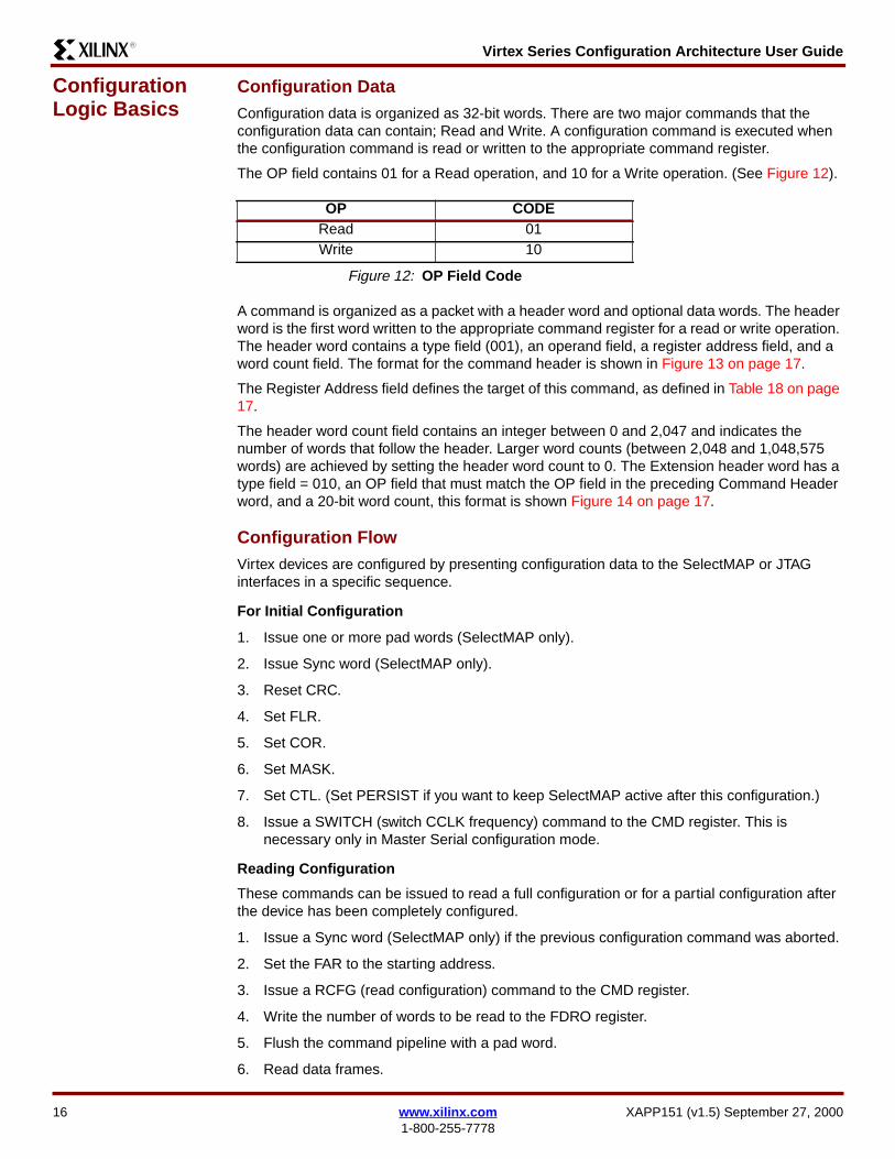
Virtex Series Configuration Architecture User GuideR13
ConfigurationLogic Basics
Configuration DataConfiguration data is organized as 32-bit words There are two major commands that theconfiguration data can contain Read and Write A configuration command is executed whenthe configuration command is read or written to the appropriate command register
The OP field contains 01 for a Read operation and 10 for a Write operation (See Figure 12)
A command is organized as a packet with a header word and optional data words The headerword is the first word written to the appropriate command register for a read or write operationThe header word contains a type field (001) an operand field a register address field and aword count field The format for the command header is shown in Figure 13 on page 17
The Register Address field defines the target of this command as defined in Table 18 on page17
The header word count field contains an integer between 0 and 2047 and indicates thenumber of words that follow the header Larger word counts (between 2048 and 1048575words) are achieved by setting the header word count to 0 The Extension header word has atype field = 010 an OP field that must match the OP field in the preceding Command Headerword and a 20-bit word count this format is shown Figure 14 on page 17
Configuration FlowVirtex devices are configured by presenting configuration data to the SelectMAP or JTAGinterfaces in a specific sequence
For Initial Configuration
1 Issue one or more pad words (SelectMAP only)
2 Issue Sync word (SelectMAP only)
3 Reset CRC
4 Set FLR
5 Set COR
6 Set MASK
7 Set CTL (Set PERSIST if you want to keep SelectMAP active after this configuration)
8 Issue a SWITCH (switch CCLK frequency) command to the CMD register This isnecessary only in Master Serial configuration mode
Reading Configuration
These commands can be issued to read a full configuration or for a partial configuration afterthe device has been completely configured
1 Issue a Sync word (SelectMAP only) if the previous configuration command was aborted
2 Set the FAR to the starting address
3 Issue a RCFG (read configuration) command to the CMD register
4 Write the number of words to be read to the FDRO register
5 Flush the command pipeline with a pad word
6 Read data frames
OP CODERead 01Write 10
Figure 12 OP Field Code
16 wwwxilinxcom XAPP151 (v15) September 27 20001-800-255-7778
Virtex Series Configuration Architecture User GuideR13
Writing Configuration
These commands can be issued either as part of an initial configuration or for a partialconfiguration after the device has been configured
1 Issue a Sync word (SelectMAP only) if the previous configuration command was aborted
2 If the frames being written can cause contention then assert the GHIGH_B signal
3 Set the FAR to the starting address
4 Issue a WCFG (write configuration) command to the CMD register
5 Write the number of words to be written to the FDRI register
6 Write data frames
7 If the GHIGH_B signal was asserted de-assert it by writing the LFRM (Last Frame)command to the CMD register and write one pad frame
ConfigurationRegisters
Configuration logic is accessed and controlled via a collection of 32-bit registers called theconfiguration registers (see Table 18) Registers are described in the following sections
Type OP Register Address RSV Word Count31 30 29 28 27 26 25 24 23 22 21 20 19 18 17 16 15 14 13 12 11 10 9 8 7 6 5 4 3 2 1 00 0 1 x x 0 0 0 0 0 0 0 0 0 0 x x x x 0 0 x x x x x x x x x x x
Notes1 Locations within fields containing a zero or one must have these values An X in a bit field indicates that the value is variable and must
be set2 Heavy vertical lines are used to separate fields Light vertical lines separate nibbles in the word
Figure 13 Command Header Format
Type OP Word Count31 30 29 28 27 26 25 24 23 22 21 20 19 18 17 16 15 14 13 12 11 10 9 8 7 6 5 4 3 2 1 00 1 0 x x 0 0 0 0 0 0 0 x x x x x x x x x x x x x x x x x x x x
Notes1 Locations within fields containing a zero or one must have these values An X in a bit field indicates that the value is variable and must
be set2 Heavy vertical lines are used to separate fields Light vertical lines separate nibbles in the word
Figure 14 Large Block Count Header Extension Format
Table 18 Configuration Register Addresses
Register Name Mnemonic RW Binary Address
CRC CRC RW 0000
Frame Address FAR RW 0001
Frame Data Input FDRI W 0010
Frame Data Output FDRO R 0011
Command CMD RW 0100
Control CTL RW 0101
Control Mask MASK RW 0110
Status STAT R 0111
Legacy Output LOUT W 1000
XAPP151 (v15) September 27 2000 wwwxilinxcom 171-800-255-7778
Virtex Series Configuration Architecture User GuideR13
Command Register (CMD)The content of the Command Register (CMD) is interpreted by the configuration state machineConfiguration commands control the operation of the configuration state machine the FrameData Register (FDR) and some of the global signals The command in the Command Registeris executed each time the FAR is loaded with a new value The effect of each command isdefined in Table 19
Configuration Option COR RW 1001
Reserved mdash mdash 1010
Frame Length FLR RW 1011
Reserved mdash mdash 1100
Reserved mdash mdash 1101
Reserved mdash mdash 1110
Reserved mdash mdash 1111
Table 18 Configuration Register Addresses (Continued)
Register Name Mnemonic RW Binary Address
Table 19 Configuration Commands
Cmd Code Description
Rsvd 0000 Reserved
WCFG 0001Write Configuration Data mdash Used prior to writing configuration data to the FDRI It takes theinternal configuration state machine through a sequence of states that control the shifting of the FDRand the writing of the configuration memory (See Frame Data Input Register (FDRI) on page 24)
Rsvd 0010 Reserved
LFRM 0011Last Frame mdash This command is loaded prior to writing the last (pad) data frame if the GHIGH_Bsignal was asserted This command is not necessary if the GHIGH_B signal was not asserted Thisallows overlap of the last frame write with the release of the GHIGH_B signal
RCFG 0100Read Configuration Data mdash Used prior to reading frame data from the FDRO Similar to the WCFGcommand in its effect on the FDR (see Frame Data Output Register (FDRO) on page 24)
START 0101Begin Startup Sequence mdash Starts the startup sequence This command is also used to start ashutdown sequence prior to partial re-configuration The Startup Sequence begins with the nextsuccessful CRC check (see Cyclic Redundancy Check (CRC) on page 22)
RCAP 0110Reset Capture mdash Used when performing capture in single-shot mode This command must be usedto reset the capture signal if single-shot capture has been selected
RCRC 0111 Reset CRC mdash Used to reset CRC register (see Cyclic Redundancy Check (CRC) on page 22)
AGHIGH 1000Assert GHIGH_B Signal mdash Used prior to re-configuration to prevent contention while writing newconfiguration data All CLB outputs and signals are forced to a one
SWITCH 1001Switch CCLK Frequency mdash Used to change (increase) the frequency of the Master CCLK Thenew frequency is specified in Table 21
Rsvd 1010 Reserved
Rsvd 1011 Reserved
Rsvd 1100 Reserved
18 wwwxilinxcom XAPP151 (v15) September 27 20001-800-255-7778
Virtex Series Configuration Architecture User GuideR13
Configuration Option Register (COR)The Configuration Option Register (COR) is used to select configuration options that areillustrated in Figure 15 and defined in Table 20 Entries in this table are further explained in thefollowing tables
Rsvd 1101 Reserved
Rsvd 1110 Reserved
Rsvd 1111 Reserved
Table 19 Configuration Commands (Continued)
Cmd Code Description
DO
NE
_PIP
E
DR
IVE
_DO
NE
SIN
GLE
OS
CF
SE
L
SS
CLK
SR
C
LOC
K_W
AIT
SH
UT
DO
WN
DO
NE
_CY
CLE
LCK
_CY
CLE
GT
S_C
YC
LE
GW
E_C
YC
LE
GS
R_C
YC
LE
31 30 29 28 27 26 25 24 23 22 21 20 19 18 17 16 15 14 13 12 11 10 9 8 7 6 5 4 3 2 1 00 x x x x x x x x x x x x x x x x x x x x x x x x x x x x x x x
Notes1 Locations within fields containing a zero or one must have these values An X in a bit field indicates that the value is variable and must
be set2 Heavy vertical lines are used to separate fields Light vertical lines separate nibbles in the word
Figure 15 COR (Configuration of Option Register) Fields
XAPP151 (v15) September 27 2000 wwwxilinxcom 191-800-255-7778
Virtex Series Configuration Architecture User GuideR13
Table 21 shows the allowed values for the OSCFSEL field of the COR Setting OSCFSEL toone of these values will set the Master CCLK frequency to the specified value
Table 20 Configuration Option Register Fields
Field Bit Indices DescriptionBitgenDefault
DONE_PIPE 30
0 No pipeline stage for DONEIN
1 Add pipeline stage to DONEINFPGA waits on DONE that is delayed by one (1) cycle of the StartupClkrather than the pin itself Use this option when StartupClk is running at highspeeds
0
DRIVE_DONE 290 DONE pin is open drain
1 DONE pin is actively driven high0
SINGLE 28 Readback capture is one-shot 0
OSCFSEL 2722 Select CCLK frequency in Master Serial configuration mode 2
SSCLKSRC 2120
Startup sequence clock source00 Cclk01 UserClk1x JTAGClk
0
LOCK_WAIT 1916
4-bit mask indicating which DLL lock signals to wait for during LCK cycleThe 4 bits (from MSB to LSB) correspond to DLLs TL=3 TR=2 BL=1BR=0 (top-left top-right etc) In Virtex-E devices where there are 8 DLLseach mask bit applies to the 2 DLLs in that quadrant of the device Thedefault is not to wait for any DLL lock signals
0
SHUTDOWN 15
Indicate whether doing a startup or shutdown sequence
0 Startup
1 Shutdown sequence
0
DONE_CYCLE 1412 Startup phase in which DONE pin is released 3
LCK_CYCLE 119 Stall in this startup phase until DLL locks are asserted 7
GTS_CYCLE 86 Startup phase in which IOs switch from tri-state to user design 4
GWE_CYCLE 53 Startup phase in which the global write-enable is asserted 5
GSR_CYCLE 20 Startup phase in which the global setreset is negated 5
Table 21 OSCFSEL-Specified Master CCLK Frequencies)
CCLK(MHz) OSCFSEL
CCLK(MHz) OSCFSEL
CCLK(MHz) OSCFSEL
43 000010 13 001010 41 100111
54 010001 15 001101 45 110011
69 000100 20 010111 51 101010
81 000101 26 011010 55 110100
20 wwwxilinxcom XAPP151 (v15) September 27 20001-800-255-7778
Virtex Series Configuration Architecture User GuideR13
Table 22 shows the values of the DONE_CYCLE LCK_CYCLE GTS_CYCLE GWE_CYCLEand GSR_CYCLE fields in COR This table shows the step in the start-up sequence when eachof these signals becomes active
Control Register (CTL)The Control Register (CTL) fields are illustrated in Figure 16 on page 21 and defined inTable 23
92 000110 30 011101 60 101101
100 000111 34 110010 mdash mdash
Notes1 These values are accurate to +45 ndash 30
Table 22 COR Startup Cycle Fields
FieldValue
DONE_CYCLE(DONE Active)
GTS_CYCLE(GTS_CFGInactive)
GSR_CYCLE(GSR Inactive)
GWE_CYCLE(GWE Active) LCK_CYCLE
000 1 1 1 1 0
001 2 2 2 2 1
010 3 3 3 3 2
011 4 (default) 4 4 4 3
100 5 5 (default) 5 5 4
101 6 6 6 (default) 6 (default) 5
110 mdash DoneIndagger DoneIndagger DoneIndagger 6
111 Keep State Keep State Keep State Keep State Donrsquot Wait(default)
Notes1 dagger DONE if DonePipe = No else the delayed version of DONE
Table 21 OSCFSEL-Specified Master CCLK Frequencies) (Continued)
CCLK(MHz) OSCFSEL
CCLK(MHz) OSCFSEL
CCLK(MHz) OSCFSEL
SB
ITS
PE
RS
IST
GT
S_U
SR
_B
31 30 29 28 27 26 25 24 23 22 21 20 19 18 17 16 15 14 13 12 11 10 9 8 7 6 5 4 3 2 1 00 0 0 0 0 0 0 0 0 0 0 0 0 0 0 0 0 0 0 0 0 0 0 x x x 0 0 0 0 0 x
Notes1 Locations within fields containing a zero or one must have these values An X in a bit field indicates that the value is variable and must
be set2 Heavy vertical lines are used to separate fields Light vertical lines separate nibbles in the word
Figure 16 Control Register Fields
XAPP151 (v15) September 27 2000 wwwxilinxcom 211-800-255-7778
Virtex Series Configuration Architecture User GuideR13
Cyclic Redundancy Check (CRC)A data input error checking mechanism is provided through the Cyclic Redundancy Check(CRC) register When data is written to any configuration register (except LOUT) a 16-bit CRCvalue is calculated using both the register data and the address This value is saved in the CRCregister At the end of any series of writes a pre-calculated CRC block-check value may bewritten to the CRC register If the resulting value is non-zero an error is indicated TheCRC_ERROR bit is accessible through the status register If a CRC error is detectedconfiguration logic is put in the ERROR mode The following section is an algorithm forcomputing CRC
CRC Algorithm Initialization bcc = 0skip_pad = truemore_words = true Check for write operation do
w = next_wordif (w[3127] == rsquo00101rsquo)
A Read OP Donrsquot use in CRCwc = w[100]if (wc == 0)
w = next_wordwc = w[190]
while (wc-- gt 0)
w = next_word
elsif (w[3127] == rsquo00110rsquo)
A Write OP Use in CRC addr = w[1613]if (addr Π0124569DB)
wc = w[100]if (wc == 0)
wc is in next word w = next_wordwc = w[190]
while (wc-- gt 0)
w = next_wordsw[350] = addr wordfor (i=0 ilt36 i++)
Table 23 Control Register Bits
NameBit
Indices Description
SBITS 87 Security level0 ReadWrite OK (default)1 Readback disabled23 Readback disabled Writing disabled except CRCregister
PERSIST 6 Configuration interface remains after configuration0 No (default)1 Yes
GTS_USR_B 0 Active-low global tristate IOs Turn off pull-ups ifGTS_CFG_B is also asserted
22 wwwxilinxcom XAPP151 (v15) September 27 20001-800-255-7778
Virtex Series Configuration Architecture User GuideR13
x16 = bcc[15] XOR sw[i]x15 = bcc[14] XOR x16x2 = bcc[1] XOR x16bcc[150] =
x15bcc[132]x2bcc[0]x16 Note the bit order crc[150] = bcc[015]
else
Pad word - ignore
while (more_words)
Frame Address Register (FAR)The Frame Address Register (FAR) holds the address of the current frame The address isdivided into three parts the block type the major address and the minor address The blocktype field indicates whether the CLB or block RAM address space is used The command in thecommand register is executed each time the FAR is loaded with a new value
The major address selects the CLB or RAM column the minor address selects the frame withinthe column The minor address is incremented each time a full data frame is read from orwritten to the frame data register If the last frame within the CLB column is selected when theincrement occurs the major address is incremented and the minor address is reset to zerootherwise the minor address is incremented However the block RAM major address is notincremented automatically
See Figure 18 for the definitions of valid values for the block type field The FAR field definitionsare shown in Figure 19
Figure 17 CRC Calculation Register
Note the Block RAM Major Address is not incremented automatically To address a differentBlock RAM Content column the FAR must be loaded with the new Major Address
Type CodesCLB 00RAM 01
Figure 18 Block Type Codes
x151_17_021100
15141312111098765432
1013
01234526272829303101
Address 32-bit Data Word
CRC Calculation Register
CRC Data Input Register
CRC Register [310]
DATA_IN
SHIFT
23
16-bit CRC13150
0000 0000 0000 0000133116
1313
XAPP151 (v15) September 27 2000 wwwxilinxcom 231-800-255-7778
Virtex Series Configuration Architecture User GuideR13
Frame Data Input Register (FDRI)The Frame Data Input Register (FDRI) is used to load configuration frame data into a Virtexdevice
The Frame Data Register (FDR) is a shift register into which data is loaded prior to transfer tothe configuration memory Configuration data is written to the Virtex device by loading thecommand register with the WCFG command and then loading the FDR with at least two framesof 32-bit words
The write operation is pipelined such that the first frame of data is written to the configurationmemory while the second frame is being shifted in The last frame (the pad frame) is alwaysdummy data which is not actually written to the configuration memory Each frame write mustinclude enough 32 bit data words to load the frame fully There is one pad word at the end ofeach frame which is required for the pipelining hardware
Frame Data Output Register (FDRO)The Frame Data Output Register (FDRO) is for reading configuration data or captured datafrom the Virtex device a process called readback Readback is performed by loading thecommand register with the RCFG command and then addressing the FDRO with a readcommand
Frame Length Register (FLR)Near the beginning of the configuration bitstream the Frame Length Register (FLR) is writtenwith the length of a frame as measured in 32-bit words This length count is used to providesequencing information for the configuration read and write operations Note that the FLR mustbe written before any FDR operation works It is not necessary to set the FLR more than onceIf the number of bits in a frame is not evenly divisible by 32 the length count of the frame mustbe rounded up to the next highest integer The values for the FLR for all the current Virtexseries devices are given in Table 24
BlockType
Major Address(Column Address)
Minor Address(Frame Address)
31 30 29 28 27 26 25 24 23 22 21 20 19 18 17 16 15 14 13 12 11 10 9 8 7 6 5 4 3 2 1 00 0 0 0 0 x x x x x x x x x x x x x x x x x x 0 0 0 0 0 0 0 0 0
Notes1 Locations within fields containing a zero or one must have these values An X in a bit field indicates that the value is variable and must
be set2 Heavy vertical lines are used to separate fields Light vertical lines separate nibbles in the word
Figure 19 Frame Address Fields (FAR)
Note The FLR contains a value that is one less than the number of words that are read fromor written to a given frame This is because the extra word needed for pipelining is not counted
Table 24 Frame Length Register Value
Device Row times Col Frame Length Words per Frame FLR Value
XCV50E 16 times 24 384 12 11
XCV100E 20 times 30 448 14 13
XCV150 24 times 36 512 16 15
XCV200E 28 times 42 576 18 17
XCV300E 32 times 48 672 21 20
24 wwwxilinxcom XAPP151 (v15) September 27 20001-800-255-7778
Virtex Series Configuration Architecture User GuideR13
Legacy Output Register (LOUT)The Legacy Output Register (LOUT) is used for daisy chaining the configuration bitstream toother Xilinx devices Data written to the LOUT is serialized and appears on the DOUT pin
Mask Register (MASK)The Mask Register (MASK) is a mask register for writes to the CTL register A 1 in bit N of themask allows that bit position to be written in the CTL register The default value of the mask isall 0s
Status Register (STAT)The Status Register (STAT) is loaded with current values of several control or status signalsThe register can be read via the re-configuration block or via JTAG The fields in the Statusregister are illustrated in Figure 20 The values of the signals given in Table 25 on page 26 canbe read from the status register
XCV400E 40 times 60 800 25 24
XCV405E 40 times 60 800 25 24
XCV600E 48 times 72 960 30 29
XCV800 56 times 84 1088 34 33
XCV812E 56 times 84 1088 34 33
XCV1000E 64 times 96 1248 39 38
XCV1600E 72 times 108 1376 43 42
XCV2000E 80 times 120 1536 48 47
XCV2600E 92 times 138 1728 54 53
XCV3200E 104 times 156 1952 61 60
Table 24 Frame Length Register Value (Continued)
Device Row times Col Frame Length Words per Frame FLR Value
DO
NE
INIT
MO
DE
GH
IGH
_B
GS
R_B
GW
E_B
GT
S_C
FG
IN_E
RR
OR
LOC
K
CR
C_E
RR
OR
31 30 29 28 27 26 25 24 23 22 21 20 19 18 17 16 15 14 13 12 11 10 9 8 7 6 5 4 3 2 1 00 0 0 0 0 0 0 0 0 0 0 0 0 0 0 0 0 x x x x x x x x x x x x x x x
Notes1 An X in a bit field indicates that the value is variable2 Heavy vertical lines are used to separate fields Light vertical lines separate nibbles in the word
Figure 20 Status Register Fields
XAPP151 (v15) September 27 2000 wwwxilinxcom 251-800-255-7778
Virtex Series Configuration Architecture User GuideR13
ConfigurationInterface
There are two configuration interfaces to the Virtex devices mdash the bit-serial Boundary Scaninterface and the 8-bit byte-serial SelectMAP interface Conceptually XCV50 configurationdata appears as in Figure 21
Frames and words within frames are written in the same order in both configuration interfacesstarting with Frame 0 word 0 (the left-most in the picture) followed by word 1 etc Bits withineach word are written from left to right (MSB first) in the bit-serial configuration interfaces
Within the SelectMAP interface data is written a byte at a time A sample word is shown inFigure 22 The top row indicates the device pin names The bottom row indicates the bit indiceswithin a configuration word Byte 0 loads first followed by byte 1 et cetera The MSB of eachbyte (ie bits 31 23 15 and 7) is loaded on pin D0 The LSB of each byte (ie bits 24 16 8and 0) is loaded on pin D7
PartialReconfigurationof CLBs
Partial reconfiguration can be performed with and without shutting down the device Ifcontention occurs it is advised to go through a shutdown sequence prior to loadingconfiguration frames When shutting down the DONE pin will go active and pull low If this is notdesireable the DONE pin can be prevented from going low by selecting the DONE_CYCLE toKeep State (111) Similarly to prevent GSR from becoming active and reseting the currentstate the GSR_CYCLE can be set to Keep State When not shutting down changes occurframe by frame but is completely done by the end of the Last Frame packet (see Example 1)
Table 25 Status Register Bits
Name Bit Indices Description
DONE 14 Input from DONE pin
INIT 13 Value of INIT
MODE 1210 Value of M2 M1 M0 mode pins
GHIGH_B 9 0 = GHIGH_B asserted
GSR_B 8 0 = all flip-flops are ResetSet
GWE_B 7 1 = flip-flops and block RAM are write disabled
GTS_CFG 6 0 = IOs are tri-stated
IN_ERROR 5 Legacy input error
LOCK 41 Output from DLL lock signals 1 = DLL is locked
CRC_ERROR 0 Indicates that a CRC error has occurred
Data Frame 0 (11 words) Pad Word
hellip
Data Frame n (11 words) Pad WordPad Frame (12 words)
Figure 21 XCV50 Frame Padding for Reads
Figure 22 SelectMAP Byte and Bit Ordering
x151_22_021100
D0 D1 D2 D3 D4 D5 D6 D7 D0 D1 D2 D3 D4 D5 D6 D7 D0 D1 D2 D3 D4 D5 D6 D7 D0 D1 D2 D3 D4 D5 D6 D7
Byte 0 Byte 1 Byte 2 Byte 313
26 wwwxilinxcom XAPP151 (v15) September 27 20001-800-255-7778
Virtex Series Configuration Architecture User GuideR13
The DONE pin will not change in this case Figure 23 illustrates a typical shutdownreconfiguration in the CLB address space and restart sequence
Examples Several examples of reading and evaluating configuration data are provided to illustrate thefollowing
Figure 23 Typical Shutdown Reconfiguration in the CLB Address Spaceand Restart Sequence
FFFF FFFF Dummy WordAA99 5566 Sync Word Does not realign an already synchronized SelectMap port3001 2001 COR0080 FF2F Shutdown bit set optionally set bit 29 DRIVE_DONE
Alternately COR may be read bit 15 set and written back3000 8001 CMD0000 0005 Start Shutdown3000 8001 CMD0000 0007 Reset CRC0000 00000000 0000 Clock shutdown sequence0000 00000000 00003000 8001 CMD0000 0008 Assert GHIGH3000 8001 CMD0000 0001 Write Configuration3000 2001 FAR0--- ---- Block Type CLB (00) MajorMinor Address3000 4--- FDRI + Word Count if count is lt1024 Otherwise use TypeII Header
Write FRAME DATAIf CLB Frames are not written to non-consecutive addresses repeat FAR word followedby new MajorMinor Address followed by FDRI + Word Count and then Frame Data
3000 0001 Write CRC---- ---- CRC3000 8001 CMD0000 0003 LFRM3000 4--- FDRI + Word Count
Write PAD FRAME
3001 2001 COR0080 3F2D Default COR Options
Alternately COR may be read bit 15 cleared and written back3000 8001 CMD0000 0005 Begin Startup3000 0001 Write CRC---- ---- CRC
0000 00000000 0000 4 Dummy Words0000 00000000 0000
Example 1 Read and Write Semaphores in an XCV100 at CLB R1 C1 Slice 0 on page 28Example 2 Reading the Complete Configuration from an XCV50 on page 33
XAPP151 (v15) September 27 2000 wwwxilinxcom 271-800-255-7778
Virtex Series Configuration Architecture User GuideR13
Example 1 Read and Write Semaphores in an XCV100 at CLB R1 C1Slice 0Semaphores are a useful communication mechanism documented in XAPP 153 ldquoStatus andControl Semaphore Registers using Partial Reconfigurationrdquo Figure 24 shows an abstractionof a microprocessor writing control information to an FPGA and reading status informationOne convention for implementing semaphores in Virtex devices is to use two bits of a 16-bitdual-port RAM as illustrated in Figure 25 This occupies one CLB slice with the F-LUTimplementing the control semaphore and the status semaphore implemented in the G-LUTAddress 15 of the G-LUT is used for on-chip writes to the semaphore and address 14 of the F-LUT is used for on-chip reads Conversely the off-chip microprocessor is reading the G-LUT[15] and writing F-LUT[14]
Example 3 Read the Slice 0 G-LUT from CLB R1 C1 from the Complete Configuration of anXCV50 on page 34Example 4 Read the Slice 1 F-LUT from CLB R19 C16 from an XCV100 on page 36Example 5 Read All Bits in Slice 0 G-LUTs from CLB C2 and XCV50 on page 39Example 6 Read Block SelectRAM index 387 of RAM R2 C0 from an XCV100E on page 41
Figure 24 Semaphore Abstraction
x151_ 23_021400
Status13
Control13
MicroProcessor FPGA13
Semaphores13
28 wwwxilinxcom XAPP151 (v15) September 27 20001-800-255-7778
Virtex Series Configuration Architecture User GuideR13
Using a Semaphore Abstraction dual-port RAM ensures that the LUT SelectRAMs are placedin the CLB in a predictable manner When writing data to one or more LUT SelectRAMs or flip-flops on the device all bits in the frame must have valid configuration information This isassured by altering valid configurations from bitstream files or from frames read from a properlyconfigured Virtex device The latter approach is used in this example
Figure 25 Semaphore ReadWrite Implementation
Frame 47
15
14
47 46
47 46
x151_ 24_021100
Select Map
Frame 46
DING
F
13
D2D3D4 5D6 7D0D1 D D
1
111
0
111
Chip Interface
G F
13
XAPP151 (v15) September 27 2000 wwwxilinxcom 291-800-255-7778
Virtex Series Configuration Architecture User GuideR13
Attributes for this design are summarized in Table 26
From the equations in Table 7 on page 11 the values shown in Table 27 can be calculated
From off-chip for reading the G-LUT[15] bit read one frame (MNA=47) For writing the F-LUT[14] bit we show how to read then write one frame (MNA=46) as opposed to modifyingdata from a bitstream file (both are valid methods) The frames on the XCV100 contain 13 32-bit words and one pad word Remember that fm_st_wd is calculated assuming the entireconfiguration has been read However only the pad frame and then frames 46 and 47 fromMajor Address 30 are being read The desired bit is in Frame 1 word 1 which is word 15
The commands for reading both frames (and the pad frame) are given in Figure 26
Table 26 Design Attributes for Example 1
Attribute
G-LUT [15] F-LUT [14]
Read Read Write
Chip_Rows 20
Chip_Cols 30
FL 14
CLB_Row 1
CLB_Col 1
Slice 0
FG 1 0
lut_bit 15 14
RW 1 1 0
Table 27 Semaphore Example Variables Equations and Values
Variable Equation
Value(s)
G-LUT[15] F-LUT[14]
Read Read Write
MJA 1 le 302 rArr 30 ndash 1 times 2 + 2 30
MNA lut_bit + 32ndash 0 times () 47 46
fm_bit_idx 3 + 18 times 1 ndash FG + RW times 32 52 53 21
fm_st_wd 14 times (8 + (30 ndash 1) times 48+ 4647) +RW times (14 +1)= 14 times (1400 + 4647) + 14 times RW= 19600 + 14 times 4647 + 14 times RW
20272 20258 20244
fm_wd floor (2032) 1 1 0
fm_wd_bit_idx 31 + 32 times 110 ndash 525321 11 10 10
30 wwwxilinxcom XAPP151 (v15) September 27 20001-800-255-7778
Virtex Series Configuration Architecture User GuideR13
The 42 words read are shown in Figure 27 F-LUT[14] is in the second frame (frame=1word=1) at bit 10 The value read is a 1 but because the LUT bits are inverted the logic valueis zero G-LUT[15] is in word one of the third data frame (frame=2 word=1) at bit 11The valueread is a 1 which is a logic zero
InstructionData
Hex 31 30 29 28 27 26 25 24 23 22 21 20 19 18 17 16 15 14 13 12 11 10 9 8 7 6 5 4 3 2 1 0
Sync Word AA99 5566 1 0 1 0 1 0 1 0 1 0 0 1 1 0 0 1 0 1 0 1 0 1 0 1 0 1 1 0 0 1 1 0
Write next (1) word to FAR 3000 2001 0 0 1 1 0 0 0 0 0 0 0 0 0 0 0 0 0 0 1 0 0 0 0 0 0 0 0 0 0 0 0 1
CLB MJA=30 MNA=46 003C 5800 0 0 0 0 0 0 0 0 0 0 1 1 1 1 0 0 0 1 0 1 1 1 0 0 0 0 0 0 0 0 0 0
Write next word to CMD 3000 8001 0 0 1 1 0 0 0 0 0 0 0 0 0 0 0 0 1 0 0 0 0 0 0 0 0 0 0 0 0 0 0 1
Register value for RCFG 0000 0004 0 0 0 0 0 0 0 0 0 0 0 0 0 0 0 0 0 0 0 0 0 0 0 0 0 0 0 0 0 1 0 0
Read from FDRO 2800 602A 0 0 1 0 1 0 0 0 0 0 0 0 0 0 0 0 0 1 1 0 0 0 0 0 0 0 1 0 1 0 1 0
Flush pipe 0000 0000 0 0 0 0 0 0 0 0 0 0 0 0 0 0 0 0 0 0 0 0 0 0 0 0 0 0 0 0 0 0 0 0
(read 42 words)
Notes1 Binary data is grouped in two ways for ease of interpretation Thin vertical lines separate nibble boundaries Heavy vertical lines
separate field boundaries
Figure 26 Commands to Read Two Data Frames
XAPP151 (v15) September 27 2000 wwwxilinxcom 311-800-255-7778
Virtex Series Configuration Architecture User GuideR13
To write to the F-LUT semaphore start with the second data frame (frame=1) that was justread Words 1 - 13 of that frame will become words 0 - 12 of the frame to be written Word 13of this new frame is a pad word and can have any value (typically 0 is chosen) In this newframe set bit 11 of word 0 (zero) to the desired value of the semaphore A pad frame mustfollow the data frame The commands from Figure 28 write these two frames into the device atthe proper location
Frame Word 31 30 29 28 27 26 25 24 23 22 21 20 19 18 17 16 15 14 13 12 11 10 9 8 7 6 5 4 3 2 1 0
0
0 1 1 1 1 1 1 1 1 1 1 1 1 1 1 1 1 1 1 1 1 1 1 1 1 1 1 1 1 1 1 1 1
1 1 1 1 1 1 1 1 1 1 1 1 1 1 1 1 1 1 1 1 1 1 1 1 1 1 1 1 1 1 1 1 1
2 1 1 1 1 1 1 1 1 1 1 1 1 1 1 1 1 1 1 1 1 1 1 1 1 1 1 1 1 1 1 1 1
3 1 1 1 1 1 1 1 1 1 1 1 1 1 1 1 1 1 1 1 1 1 1 1 1 1 1 1 1 1 1 1 1
4 1 1 1 1 1 1 1 1 1 1 1 1 1 1 1 1 1 1 1 1 1 1 1 1 1 1 1 1 1 1 1 1
5 1 1 1 1 1 1 1 1 1 1 1 1 1 1 1 1 1 1 1 1 1 1 1 1 1 1 1 1 1 1 1 1
6 1 1 1 1 1 1 1 1 1 1 1 1 1 1 1 1 1 1 1 1 1 1 1 1 1 1 1 1 1 1 1 1
7 1 1 1 1 1 1 1 1 1 1 1 1 1 1 1 1 1 1 1 1 1 1 1 1 1 1 1 1 1 1 1 1
8 1 1 1 1 1 1 1 1 1 1 1 1 1 1 1 1 1 1 1 1 1 1 1 1 1 1 1 1 1 1 1 1
9 1 1 1 1 1 1 1 1 1 1 1 1 1 1 1 1 1 1 1 1 1 1 1 1 1 1 1 1 1 1 1 1
10 1 1 1 1 1 1 1 1 1 1 1 1 1 1 1 1 1 1 1 1 1 1 1 1 1 1 1 1 1 1 1 1
11 1 1 1 1 1 1 1 1 1 1 1 1 1 1 1 1 1 1 1 1 1 1 1 1 1 1 1 1 1 1 1 1
12 1 1 1 1 1 1 1 1 1 1 1 1 1 1 1 1 1 1 1 1 1 1 1 1 1 1 1 1 1 1 1 1
13 1 1 1 1 1 1 1 1 1 1 1 1 1 1 1 1 1 1 1 1 1 1 1 1 1 1 1 1 1 1 1 1
1
0 0 0 0 0 0 0 0 0 0 0 0 0 0 0 0 0 0 0 0 0 0 0 0 0 0 0 0 0 0 0 0 0
1 1 0 0 0 0 0 0 0 0 0 0 0 1 0 0 0 0 1 1 0 1 1 0 0 0 0 0 0 0 0 0 0 F[14]
2 1 1 1 1 1 0 1 1 0 0 0 0 1 1 1 1 0 0 1 1 1 1 1 0 1 1 0 0 0 0 0 0
3 0 0 0 0 1 1 1 1 1 0 1 1 0 0 0 0 0 0 0 0 0 0 1 1 1 1 1 0 1 1 0 0
4 0 0 0 0 0 0 0 0 1 1 1 1 0 0 0 0 0 0 0 0 0 0 0 0 0 0 1 1 1 1 1 0
5 1 1 0 0 1 1 0 0 0 0 0 0 1 1 0 0 1 0 1 1 0 0 0 0 0 0 0 0 0 0 1 1
6 1 1 1 0 1 1 0 0 0 0 0 0 1 1 1 0 1 1 1 0 1 0 1 1 0 0 0 0 0 0 0 0
7 0 0 1 1 1 1 1 0 1 1 0 0 0 0 1 1 0 0 0 0 1 1 1 1 1 0 1 1 0 0 0 0
8 0 0 0 0 0 0 1 1 1 1 1 0 0 0 0 0 0 0 0 0 0 0 0 0 1 1 1 1 1 0 1 1
9 0 0 0 0 0 0 0 0 0 0 1 1 0 0 0 0 1 1 0 0 0 0 0 0 0 0 0 0 1 1 1 1
10 1 0 1 1 0 0 0 0 0 0 0 0 1 0 1 1 1 1 1 0 1 1 0 0 0 0 0 0 0 0 0 0
11 1 1 1 1 1 0 1 1 0 0 0 0 1 1 1 1 0 0 1 1 1 1 1 0 1 1 0 0 0 0 0 0
12 0 0 0 0 1 1 0 1 1 0 1 1 0 0 0 0 0 0 0 0 0 0 1 1 1 1 1 0 0 0 0 0
13 0 0 0 0 0 0 1 1 0 1 0 1 0 0 0 0 0 0 0 0 0 0 0 0 0 0 0 0 0 0 0 0
2
0 0 0 0 0 0 0 0 0 0 0 0 0 0 0 0 0 0 0 0 0 0 0 0 0 0 0 0 0 0 0 0 0
1 1 0 1 0 0 0 0 0 0 0 0 1 1 0 1 0 1 1 1 0 1 1 0 0 0 0 0 0 0 0 0 0 G[15]
2 1 1 1 1 1 1 1 1 0 0 0 0 1 1 1 1 0 0 1 1 1 1 1 1 1 1 0 0 0 0 0 0
3 0 0 0 0 1 1 1 1 1 1 1 1 0 0 0 0 0 0 0 0 0 0 1 0 1 1 1 1 1 1 0 0
4 0 0 0 0 0 0 0 0 1 1 1 1 0 0 0 0 0 0 0 0 0 0 0 0 0 0 1 1 1 1 1 1
5 1 1 0 0 0 0 0 0 0 0 0 0 1 1 0 0 1 1 1 1 0 0 1 0 0 0 0 0 0 0 1 1
6 1 1 1 1 1 1 0 0 0 0 0 0 1 1 1 1 1 1 1 1 1 1 1 1 0 0 0 0 0 0 0 0
7 0 0 1 1 1 1 1 1 1 1 0 0 0 0 1 1 0 0 0 0 1 1 1 1 1 1 1 1 0 0 0 0
8 0 0 0 0 0 0 1 1 1 1 1 1 0 0 0 0 0 0 0 0 0 0 0 0 1 1 1 1 1 1 1 1
9 0 0 0 0 0 0 0 0 0 0 1 1 0 0 0 0 1 1 0 0 0 0 0 0 0 0 0 0 1 1 1 1
10 1 1 1 1 0 0 0 0 0 0 0 0 1 1 1 1 1 1 1 1 1 1 0 0 0 0 0 0 0 0 0 0
11 1 1 1 1 1 1 1 1 0 0 0 0 1 1 1 1 0 0 1 1 1 1 1 1 1 1 0 0 0 0 0 0
12 0 0 0 0 1 1 0 1 1 1 1 1 0 0 0 0 0 0 0 0 0 0 1 1 1 1 1 0 1 0 0 0
13 0 0 0 0 0 1 1 0 0 1 1 1 0 0 0 0 0 0 0 0 0 0 0 0 0 0 0 0 0 0 0 0
Figure 27 Three Frames Containing the Semaphores
32 wwwxilinxcom XAPP151 (v15) September 27 20001-800-255-7778
Virtex Series Configuration Architecture User GuideR13
Example 2 Reading the Complete Configuration from an XCV50Steps
1 If flip-flop values are needed clock the on-chip signal CAPTURE to capture flip-flopvalues See the Xilinx Libraries Guide for use of the CAPTURE_VIRTEX cell
2 Write the starting frame address (CLB MJA=0 MNA=0) into the FAR
3 Write the RCFG command to the CMD register
4 Address the FDRO register with a READ operation and word count equal to the number of32-bit words in the CLB frames plus one pad frame
5 Read the data following the timing diagrams in the SelectMAP interface section
6 Write the address for RAM block 0 to the FAR
7 Address the FDRO register with a read operation and word count equal to the number of32-bit words in the RAM block plus one pad frame
8 Read the data
9 Write the address for RAM block 1 to the FAR
10 Address the FDRO register with a read operation and word count equal to the number of32-bit words in the RAM block plus one pad frame
11 Read the data
When using SelectMAP mode to read data words from the Virtex device de-assert CS de-assert WRITE assert CS then clock the data out When using JTAG load the JTAG IR
InstructionData
Hex 31 30 29 28 27 26 25 24 23 22 21 20 19 18 17 16 15 14 13 12 11 10 9 8 7 6 5 4 3 2 1 0
Sync Word AA995566
1 0 1 0 1 0 1 0 1 0 0 1 1 0 0 1 0 1 0 1 0 1 0 1 0 1 1 0 0 1 1 0
Write next (1) word to FAR 30002001
0 0 1 1 0 0 0 0 0 0 0 0 0 0 0 0 0 0 1 0 0 0 0 0 0 0 0 0 0 0 0 1
MJA=30 MNA=46 003C5C00
0 0 0 0 0 0 0 0 0 0 1 1 1 1 0 0 0 1 0 1 1 1 0 0 0 0 0 0 0 0 0 0
Write next word to CMD 30008001
0 0 1 1 0 0 0 0 0 0 0 0 0 0 0 0 1 0 0 0 0 0 0 0 0 0 0 0 0 0 0 1
Register value for WCFG 00000001
0 0 0 0 0 0 0 0 0 0 0 0 0 0 0 0 0 0 0 0 0 0 0 0 0 0 0 0 0 0 0 1
Write 28 words to FDRI 3000401C
0 0 1 1 0 0 0 0 0 0 0 0 0 0 0 0 0 1 0 0 0 0 0 0 0 0 0 1 1 1 0 0
Data Word 0 A01AEC00
1 0 1 0 0 0 0 0 0 0 0 1 1 0 1 0 1 1 1 0 1 1 0 0 0 0 0 0 0 0 0 0
Data Word 1 FF0F3FC0
1 1 1 1 1 1 1 1 0 0 0 0 1 1 1 1 0 0 1 1 1 1 1 1 1 1 0 0 0 0 0 0
Data Word 2 0FF002FC
0 0 0 0 1 1 1 1 1 1 1 1 0 0 0 0 0 0 0 0 0 0 1 0 1 1 1 1 1 1 0 0
hellip hellip hellip
Data Word 27 00000000
0 0 0 0 0 0 0 0 0 0 0 0 0 0 0 0 0 0 0 0 0 0 0 0 0 0 0 0 0 0 0 0
Notes1 Binary data is grouped in two ways for ease of interpretation Thin vertical lines separate nibble boundaries Heavy
vertical lines separate field boundaries
Figure 28 Commands to Write a Semaphore Value
XAPP151 (v15) September 27 2000 wwwxilinxcom 331-800-255-7778
Virtex Series Configuration Architecture User GuideR13
(instruction register) with the CFG_OUT instruction Then go to the SDR (Shift-DR) state andshift the data out (See Figure 29)
Example 3 Read the Slice 0 G-LUT from CLB R1 C1 from the CompleteConfiguration of an XCV50The commands for reading the bitstream from the Virtex device are given in Example 1 Readand Write Semaphores in an XCV100 at CLB R1 C1 Slice 0 on page 28 Using an XCV50device the independent attributes are show in Table 28
InstructionData
Hex 31 30 29 28 27 26 25 24 23 22 21 20 19 18 17 16 15 14 13 12 11 10 9 8 7 6 5 4 3 2 1 0
Sync Word AA99 5566 1 0 1 0 1 0 1 0 1 0 0 1 1 0 0 1 0 1 0 1 0 1 0 1 0 1 1 0 0 1 1 0
Write next word to FAR 3000 2001 0 0 1 1 0 0 0 0 0 0 0 0 0 0 0 0 0 0 1 0 0 0 0 0 0 0 0 0 0 0 0 1
CLB MJA=0 MNA=0 0000 0000 0 0 0 0 0 0 0 0 0 0 0 0 0 0 0 0 0 0 0 0 0 0 0 0 0 0 0 0 0 0 0 0
Write next word to CMDregister
3000 8001 0 0 1 1 0 0 0 0 0 0 0 0 0 0 0 0 1 0 0 0 0 0 0 0 0 0 0 0 0 0 0 1
Register value for RCFG 0000 0004 0 0 0 0 0 0 0 0 0 0 0 0 0 0 0 0 0 0 0 0 0 0 0 0 0 0 0 0 0 1 0 0
Read from FDRO register 2800 6000 0 0 1 0 1 0 0 0 0 0 0 0 0 0 0 0 0 1 1 0 0 0 0 0 0 0 0 0 0 0 0 0
15876 words 4800 3E04 0 1 0 0 1 0 0 0 0 0 0 0 0 0 0 0 0 0 1 1 1 1 1 0 0 0 0 0 0 1 0 0
Flush pipe 0000 0000 0 0 0 0 0 0 0 0 0 0 0 0 0 0 0 0 0 0 0 0 0 0 0 0 0 0 0 0 0 0 0 0
(Read 15876 words)Write to FAR register 3000 2001 0 0 1 1 0 0 0 0 0 0 0 0 0 0 0 0 0 0 1 0 0 0 0 0 0 0 0 0 0 0 0 1
RAM MJA=0 MNA=0 0200 0000 0 0 0 0 0 0 1 0 0 0 0 0 0 0 0 0 0 0 0 0 0 0 0 0 0 0 0 0 0 0 0 0
Read 780 words fromFDRO reg
2800 630C 0 0 1 0 1 0 0 0 0 0 0 0 0 0 0 0 0 1 1 0 0 0 1 1 0 0 0 0 1 1 0 0
Flush pipe 0000 0000 0 0 0 0 0 0 0 0 0 0 0 0 0 0 0 0 0 0 0 0 0 0 0 0 0 0 0 0 0 0 0 0
(Read 780 words)Write to FAR register 3000 2001 0 0 1 1 0 0 0 0 0 0 0 0 0 0 0 0 0 0 1 0 0 0 0 0 0 0 0 0 0 0 0 1
RAM MJA=1 MNA=0 0202 0000 0 0 0 0 0 0 1 0 0 0 0 0 0 0 1 0 0 0 0 0 0 0 0 0 0 0 0 0 0 0 0 0
Read 780 words fromFDRO reg
2800 630C 0 0 1 0 1 0 0 0 0 0 0 0 0 0 0 0 0 1 1 0 0 0 1 1 0 0 0 0 1 1 0 0
Flush pipe 0000 0000 0 0 0 0 0 0 0 0 0 0 0 0 0 0 0 0 0 0 0 0 0 0 0 0 0 0 0 0 0 0 0 0
(Read 780 words)
Figure 29 Example 2 - Read Complete Configuration for XCV50
Table 28 XCV50 Independent Attributes
Independent Attributes Values
Chip_Rows 16
Chip_Cols 24
FL 12
CLB_Row 1
CLB_Col 1
FG 1
Slice 0
RW 1
34 wwwxilinxcom XAPP151 (v15) September 27 20001-800-255-7778
Virtex Series Configuration Architecture User GuideR13
From the equations given earlier in Table 7 calculating the range of values for fm_st_wdindicates that the word 13740 of the configuration is the starting word of the 12-word (FL=12)frame containing bit 0 of the G-LUT in Slice 0 of CLB R1C1 (Table 29)
The configuration bits for the given frame are as follows G-LUT[0] is in fm_wd=0 at bit 11
All 16 LUT SelectRAM bits are in the following words at the same bit index 11
Table 29 Variables Equations and Values for Slice 0 G-LUT
Variables Equations Values
MJA 1 le 242 rArr 24 ndash 1times 2 + 2 24
MNA 0 times (hellip) + lut_bit + 32 0 321 332 343 35
4 365 376 387 39
8 409 41
10 4211 43
12 4413 4514 4615 47
fm_bit_idx 3 + 18 times 1 ndash1 + RW times 32 52
fm_st_wd 12 times (8+ (24 ndash1) times 48 + [3247]) +1 x 12= 12 times (1112 + [3247]) +12= 13356 + 12 times 3247]
1374013920
fm_wd floor(5232) 1
fm_wd_bit_idx 31 + 32 ndash 52 11
BitstreamWord
Frame 32-bit Word FrameWord31 30 29 28 27 26 25 24 23 22 21 20 19 18 17 16 15 14 13 12 11 10 9 8 7 6 5 4 3 2 1 0
13740 0 0 0 0 0 0 0 0 0 0 0 0 0 0 0 0 0 0 0 0 0 0 0 0 0 0 0 0 0 0 0 0 013741 0 0 1 0 1 0 0 0 0 0 0 0 0 1 0 1 0 1 0 0 1 1 1 0 0 0 0 0 0 0 0 0 113742 1 0 1 1 0 0 1 1 0 0 0 0 0 0 0 0 0 0 1 0 1 1 0 0 1 1 0 0 0 0 0 0 213743 0 0 0 0 1 0 1 1 0 0 1 1 0 0 0 0 0 0 0 0 0 0 1 0 1 1 0 0 1 1 0 0 313744 0 0 0 0 0 0 0 0 1 0 1 1 0 0 1 1 0 0 0 0 0 0 0 0 0 0 1 0 1 1 0 0 413745 1 1 0 0 0 0 0 0 0 0 0 0 1 0 1 1 0 0 1 1 0 0 0 0 0 0 0 0 0 0 1 0 513746 1 1 0 0 1 1 0 0 0 0 0 0 0 0 0 0 1 0 1 1 0 0 1 1 0 0 0 0 0 0 0 0 613747 0 0 1 0 1 1 0 0 1 1 0 0 0 0 0 0 0 0 0 0 1 0 1 1 0 0 1 1 0 0 0 0 713748 0 0 0 0 0 0 1 0 1 1 0 0 1 1 0 0 0 0 0 0 0 0 0 0 1 0 1 1 0 0 1 1 813749 0 0 0 0 0 0 0 0 0 0 1 0 1 1 0 0 1 1 0 0 0 0 0 0 0 0 0 0 1 0 1 1 913750 0 0 1 1 0 0 0 0 0 0 0 0 0 0 1 0 1 1 0 0 1 0 1 0 0 0 0 0 0 0 0 0 1013751 0 1 0 1 0 0 0 0 0 0 0 0 0 0 0 0 0 0 0 0 0 0 0 0 0 0 0 0 0 0 0 0 11
Figure 30 Configuration Bits for Slice 0 CLB R1C1 G-LUT [0]
XAPP151 (v15) September 27 2000 wwwxilinxcom 351-800-255-7778
Virtex Series Configuration Architecture User GuideR13
The 16 bits are LUT[150]=0111111111111111 The LUT SelectRAM bits are inverted from theirlogic values The ldquologicalrdquo contents are LUT[150]=1000000000000000 Thus this G-LUTimplements a 4-input AND function
Example 4 Read the Slice 1 F-LUT from CLB R19 C16 from an XCV100Commands for reading the bitstream from the Virtex device are given in Figure 32 Use thefollowing independent attributes to find the given F-LUT
From the equations in Table 7 on page 11 calculating fm_st_wd indicates the starting wordwith respect to a configuration that starts at MJA=0 MNA=0 Because the frames we are
BitstreamWord
Frame 32-bit Word
LUT Bit31 30 29 28 27 26 25 24 23 22 21 20 19 18 17 16 15 14 13 12 11 10 9 8 7 6 5 4 3 2 1 0
13741 0 0 1 0 1 0 0 0 0 0 0 0 0 1 0 1 0 1 0 0 1 1 1 0 0 0 0 0 0 0 0 0 0
13753 1 0 1 0 0 0 0 0 0 0 0 0 0 0 0 1 0 0 0 1 1 1 0 0 0 0 0 0 0 0 0 0 1
13765 1 0 1 0 1 0 0 0 0 0 0 0 1 0 0 0 0 0 0 1 1 1 1 0 0 0 0 0 0 0 0 0 2
13777 0 0 0 0 1 0 0 0 0 0 0 1 1 1 0 1 1 0 1 0 1 1 0 0 0 0 0 0 0 0 0 0 3
13789 0 1 0 0 0 0 0 0 0 0 0 0 0 1 0 1 1 1 1 1 1 1 1 0 0 0 0 0 0 0 0 0 4
13801 1 0 1 0 1 0 0 0 0 0 0 1 0 0 0 1 1 0 0 1 1 1 0 0 0 0 0 0 0 0 0 0 5
13813 0 0 0 1 0 0 0 0 0 0 0 0 0 0 0 0 1 0 0 1 1 1 0 0 0 0 0 0 0 0 0 0 6
13825 0 1 1 0 1 0 0 0 0 0 0 1 0 1 0 0 1 1 0 0 1 1 0 0 0 0 0 0 0 0 0 0 7
13837 1 0 1 1 1 0 0 0 0 0 0 1 0 1 0 1 1 0 0 0 1 1 0 0 0 0 0 0 0 0 0 0 8
13849 1 0 0 0 0 0 0 0 0 0 0 0 0 0 0 0 1 1 1 0 1 1 0 0 0 0 0 0 0 0 0 0 9
13861 1 0 0 0 0 0 0 0 0 0 0 1 0 0 0 0 1 1 1 1 1 1 1 0 0 0 0 0 0 0 0 0 10
13873 1 0 0 0 0 0 0 1 0 0 0 0 0 1 0 0 0 1 1 0 1 1 0 0 0 1 0 0 0 0 0 0 11
13885 1 0 0 0 0 0 0 0 0 0 0 0 0 1 0 1 0 0 1 0 1 1 0 0 0 0 0 0 0 0 0 0 12
13897 0 0 0 0 1 0 0 0 0 0 0 0 0 1 0 0 0 0 0 0 1 1 0 0 0 0 0 0 0 0 0 0 13
13909 1 0 0 0 0 0 0 0 0 0 0 0 1 1 0 1 0 1 1 0 1 1 0 0 0 0 0 0 0 0 0 0 14
13921 1 0 1 0 0 0 0 0 0 0 0 1 1 1 0 1 1 1 1 1 0 1 0 0 0 0 0 0 0 0 0 0 15
Figure 31 Location of all 16 LUT SelectRAM Bits
Table 30 Virtex Bitstream Command Attributes
Independent Attributes Values
Chip_Rows 20
Chip_Cols 30
FL 14
CLB_Row 19
CLB_Col 16
FG 0
Slice 1
RW 1
36 wwwxilinxcom XAPP151 (v15) September 27 20001-800-255-7778
Virtex Series Configuration Architecture User GuideR13
interested in start at MJA=1 MNA=0 which is fm_st_wd = 126 so the first 126 words are notneeded (0ndash125) Therefore to find the given Slice 1 F-LUT see Table 31
Sixteen frames need to be read one for each bit in the LUT SelectRAM The bits in LUTSelectRAMs in Slice 1 occur in the opposite order that they do for Slice 0 LUT SelectRAMs
Frames are read sequentially with ascending addresses If read in LUT bit order LUT[0]LUT[1] hellip LUT[15] These are stored in descending addresses which require 16 separateread operations each reading one data frame and one pad frame However if read inascending address order LUT[15] LUT[14] hellip LUT[0] all 16 data frames are read with asingle read operation This requires only one pad frame for all 16 frames Thus it takes lesstime to read ascending frames starting at MJA=1 MNA=0 and finishing with frame MJA=1MNA=15 The frames in the XCV100 contain 14 32-bit words and a single pad wordCommands for reading only the F-LUT data are given in Figure 32
Table 31 Variables Equations and Values for Slice 1 F-LUT
Variables Equations Values
MJA 16 gt 302 rArr 2times16 ndash 30 ndash1 1
MNA lut_bit + 32 ndash Slice times (2 times lut_bit +17)= [015] + 32 ndash (2 times [015] + 17)= 15 ndash [015]
0 151 142 133 12
4 115 106 97 8
8 79 6
10 511 4
12 313 214 115 0
fm_bit_idx 3 + 18 times 19 ndash 0+ 32 377
fm_st_wd 14 times (8 + (1ndash 1) times 48 + [150]) +1 times 14= 14 times (8 + [150]) +14= 126 + 14 times [150]
= 336126
fm_wd floor(37732) 11
fm_wd_bit_idx 31 + 32 times 11 ndash 377 6
XAPP151 (v15) September 27 2000 wwwxilinxcom 371-800-255-7778
Virtex Series Configuration Architecture User GuideR13
The 377th bit of each frame is the bit in the F-LUT This LUT SelectRAM bit is in the framersquosword index 11 bit index 6
The configuration bits for the given frame in Figure 33 are as follows LUT Bit 15 is in MJA=1MNA=0 fm_wd=11 at bit 6
LUT bit 0 is in MJA=1 MNA=15 fm_wd=11 at bit 6
InstructionData
Hex 31 30 29 28 27 26 25 24 23 22 21 20 19 18 17 16 15 14 13 12 11 10 9 8 7 6 5 4 3 2 1 0
Sync Word AA99 5566 1 0 1 0 1 0 1 0 1 0 0 1 1 0 0 1 0 1 0 1 0 1 0 1 0 1 1 0 0 1 1 0
Write next (1) word to FAR 3000 2001 0 0 1 1 0 0 0 0 0 0 0 0 0 0 0 0 0 0 1 0 0 0 0 0 0 0 0 0 0 0 0 1
CLB MJA = 1 MNA = 0 0002 0000 0 0 0 0 0 0 0 0 0 0 0 0 0 0 1 0 0 0 0 0 0 0 0 0 0 0 0 0 0 0 0 0
Write next word to CMD 3000 8001 0 0 1 1 0 0 0 0 0 0 0 0 0 0 0 0 1 0 0 0 0 0 0 0 0 0 0 0 0 0 0 1
Register value for RCFG 0000 0004 0 0 0 0 0 0 0 0 0 0 0 0 0 0 0 0 0 0 0 0 0 0 0 0 0 0 0 0 0 1 0 0
Read from FDRO 2800 60EE 0 0 1 0 1 0 0 0 0 0 0 0 0 0 0 0 0 1 1 0 0 0 0 0 1 1 1 0 1 1 1 0
Flush pipe 0000 0000 0 0 0 0 0 0 0 0 0 0 0 0 0 0 0 0 0 0 0 0 0 0 0 0 0 0 0 0 0 0 0 0
(Read 238 words)
Figure 32 Commands to read Slice 1 F-LUT
Frame WordFrame 32-bit Word
31 30 29 28 27 26 25 24 23 22 21 20 19 18 17 16 15 14 13 12 11 10 9 8 7 6 5 4 3 2 1 0
0 0 0 0 0 0 0 0 0 0 0 0 0 0 0 0 0 0 0 0 0 0 0 0 0 0 0 0 0 0 0 0 0
1 1 1 0 0 0 0 0 0 0 0 0 0 0 1 0 1 1 1 1 1 1 1 0 0 0 0 0 0 0 0 0 0
2 1 1 1 1 1 1 1 1 0 0 0 0 0 0 0 0 0 0 1 1 1 1 1 1 1 1 0 0 0 0 0 0
3 0 0 0 0 1 1 1 1 1 1 1 1 0 0 0 0 0 0 0 0 0 0 1 1 1 1 1 1 1 1 0 0
4 0 0 0 0 0 0 0 0 1 1 1 1 1 1 1 1 0 0 0 0 0 0 0 0 0 0 1 1 1 1 1 1
5 1 1 0 0 0 0 0 0 0 0 0 0 1 1 1 1 1 1 1 1 0 0 0 0 0 0 0 0 0 0 1 1
6 1 1 1 1 1 1 0 0 0 0 0 0 0 0 0 0 1 1 1 1 1 1 1 1 0 0 0 0 0 0 0 0
7 0 0 1 1 1 1 1 1 1 1 0 0 0 0 0 0 0 0 0 0 1 1 1 1 1 1 1 1 0 0 0 0
8 0 0 0 0 0 0 1 1 1 1 1 1 1 1 0 0 0 0 0 0 0 0 0 0 1 1 1 1 1 1 1 1
9 0 0 0 0 0 0 0 0 0 0 1 1 1 1 1 1 1 1 0 0 0 0 0 0 0 0 0 0 1 1 1 1
10 1 1 1 1 0 0 0 0 0 0 0 0 0 0 1 1 1 1 1 1 1 1 0 0 0 0 0 0 0 0 0 0
11 1 1 1 1 1 1 1 1 0 0 0 0 0 0 0 0 0 0 1 1 1 1 1 1 1 0 0 0 0 0 0 0
12 0 0 0 0 1 1 1 1 1 1 1 1 0 0 0 0 0 0 0 0 0 0 1 1 1 1 1 1 0 0 0 0
13 0 0 0 0 0 0 0 0 0 1 1 1 0 0 0 0 0 0 0 0 0 0 1 1 1 1 1 1 0 0 0 0
Figure 33 Frame Containing F-LUT[15]
Bit streamWord
Frame 32-bit WordFmWd31 30 29 28 27 26 25 24 23 22 21 20 19 18 17 16 15 14 13 12 11 10 9 8 7 6 5 4 3 2 1 0
336 0 0 0 0 0 0 0 0 0 0 0 0 0 0 0 0 0 0 0 0 0 0 0 0 0 0 0 0 0 0 0 0 0337 0 1 0 0 1 0 0 0 0 0 0 1 0 1 0 0 1 1 0 0 1 1 0 0 0 0 0 0 0 0 0 0 1338 1 0 1 1 0 0 1 1 0 0 0 0 0 0 0 0 0 0 1 0 1 1 0 0 1 1 0 0 0 0 0 0 2339 0 0 0 0 1 0 1 1 0 0 1 1 0 0 0 0 0 0 0 0 0 0 1 0 1 1 0 0 1 1 0 0 3340 0 0 0 0 0 0 0 0 1 0 1 1 0 0 1 1 0 0 0 0 0 0 0 0 0 0 1 0 1 1 0 0 4341 1 1 0 0 0 0 0 0 0 0 0 0 1 0 1 1 0 0 1 1 0 0 0 0 0 0 0 0 0 0 1 0 5342 1 1 0 0 1 1 0 0 0 0 0 0 0 0 0 0 1 0 1 1 0 0 1 1 0 0 0 0 0 0 0 0 6343 0 0 1 0 1 1 0 0 1 1 0 0 0 0 0 0 0 0 0 0 1 0 1 1 0 0 1 1 0 0 0 0 7
Figure 34 Frame Containing F-LUT [0]
38 wwwxilinxcom XAPP151 (v15) September 27 20001-800-255-7778
Virtex Series Configuration Architecture User GuideR13
For the sake of brevity here are the sixteen 11th words in the order they appear in thebitstream
The bits are LUT[150]=0111111111111111 The LUT SelectRAM bits are inverted from thelogic sense The logical contents are LUT[150]=1000000000000000 Thus this F-LUTimplements a 4-input AND gate
Example 5 Read All Bits in Slice 0 G-LUTs from CLB C2 and XCV50Given the following attributes the necessary values to find the G-LUT data can be computed
344 0 0 0 0 0 0 1 0 1 1 0 0 1 1 0 0 0 0 0 0 0 0 0 0 1 0 1 1 0 0 1 1 8345 0 0 0 0 0 0 0 0 0 0 1 0 1 1 0 0 1 1 0 0 0 0 0 0 0 0 0 0 1 0 1 1 9346 0 0 1 1 0 0 0 0 0 0 0 0 0 0 1 0 1 1 0 0 1 1 0 0 0 0 0 0 0 0 0 0 10347 1 1 1 1 1 0 1 1 0 0 0 0 0 0 0 0 0 0 1 0 1 1 1 0 1 1 0 1 0 0 0 0 11348 0 0 0 0 1 1 1 0 1 0 1 1 0 0 0 0 0 0 0 0 0 0 1 1 1 1 0 1 0 0 0 0 12349 0 0 0 0 0 1 0 0 0 0 1 0 0 0 0 0 0 0 0 0 0 0 0 0 0 0 0 0 0 0 0 0 13
Bit streamWord
Frame 32-bit WordFmWd31 30 29 28 27 26 25 24 23 22 21 20 19 18 17 16 15 14 13 12 11 10 9 8 7 6 5 4 3 2 1 0
Figure 34 Frame Containing F-LUT [0]
BitstreamWord
Frame 32-bit WordLUT Bit31 30 29 28 27 26 25 24 23 22 21 20 19 18 17 16 15 14 13 12 11 10 9 8 7 6 5 4 3 2 1 0
137 1 1 1 1 1 1 1 1 0 0 0 0 0 0 0 0 0 0 1 1 1 1 1 1 1 0 0 0 0 0 0 0 15151 1 0 1 1 1 0 1 1 0 0 0 0 0 0 0 0 0 0 1 0 1 1 1 0 1 1 0 0 0 0 0 0 14165 1 0 1 1 0 0 1 1 0 0 0 0 0 0 0 0 0 0 1 0 1 1 1 0 1 1 0 0 0 0 0 0 13179 1 0 1 1 1 0 1 1 0 0 0 0 0 0 0 0 0 0 1 0 1 1 1 0 1 1 0 0 0 0 0 0 12193 1 1 1 1 1 0 1 1 0 0 0 0 0 0 0 0 0 0 1 1 1 1 1 0 1 1 0 0 0 0 0 0 11207 1 1 1 1 1 1 1 1 0 0 0 0 0 0 0 0 0 0 1 1 1 1 1 1 1 1 1 0 1 0 0 0 10221 1 1 1 1 1 0 1 1 0 0 0 0 0 0 0 0 0 0 1 1 1 1 1 0 1 1 0 0 0 0 0 0 9235 1 0 1 1 1 0 1 1 0 0 0 0 0 0 0 0 0 0 1 0 1 1 1 0 1 1 0 0 0 0 0 0 8249 1 0 1 1 0 0 1 1 0 0 0 0 0 0 0 0 0 0 1 0 1 1 0 0 1 1 0 0 0 0 0 0 7263 1 0 1 1 0 1 1 1 1 0 0 0 0 0 0 0 0 0 1 0 1 1 0 1 1 1 0 0 0 0 0 0 6277 1 1 1 1 0 0 1 1 0 0 0 0 0 0 0 0 0 0 1 1 1 1 0 0 1 1 0 0 0 0 0 0 5291 1 1 1 1 1 1 1 1 0 0 0 0 0 0 0 0 0 0 1 1 1 1 1 1 1 1 0 0 0 0 0 0 4305 1 1 1 1 1 0 1 1 0 0 0 0 0 0 0 0 0 0 1 1 1 1 1 0 1 1 0 0 0 0 0 0 3319 1 0 1 1 0 1 1 1 0 0 0 0 0 0 0 0 0 0 1 0 1 1 0 1 1 1 0 0 0 0 0 0 2333 1 0 1 1 0 0 1 1 0 0 0 0 0 0 0 0 0 0 1 0 1 1 0 0 1 1 0 0 0 0 0 0 1347 1 1 1 1 1 0 1 1 0 0 0 0 0 0 0 0 0 0 1 0 1 1 1 0 1 1 0 1 0 0 0 0 0
Figure 35 Sixteen Words Containing the F-LUT bit
Table 32 All Bits Slice 0 GndashLUTs from CLB C2 and XCV50
Independent Attributes Values
Chip_Rows 16
Chip_Cols 24
FL 12
CLB_Row 116
CLB_Col 2
XAPP151 (v15) September 27 2000 wwwxilinxcom 391-800-255-7778
Virtex Series Configuration Architecture User GuideR13
From the equations in Table 7 the dependent variables can be calculated
Note that fm_bit_idx fm_wd and fm_wd_bit_idx have 16 values one for each row on theXCV50 Figure 37 shows where the data lies in the first frame which contains G[0] for the entirecolumn The process is the same for the other 15 frames The commands for reading the LUTSelectRAM data are given in Figure 36
From the calculation for fm_st_wd Frame 0 would start at word 12588 reading the wholeconfiguration The instructions in Figure 36 start at that word so word 0 (ignoring the 12 wordsin the pad frame) is the same as word 12588 of the entire CLB configuration The 12 words inthe frame are shown in Figure 37
FG 1
Slice 0
lut_bit 015
RW 1
Table 32 All Bits Slice 0 GndashLUTs from CLB C2 and XCV50 (Continued)
Independent Attributes Values
Table 33 Dependent Variables Equations and Values
Variables Equations Values
MJA 2 le 242 rArr 24 ndash 2times 2 + 2 22
MNAlut_bit + 32 ndash Slice times (2 times lut_bit + 17)= lut_bit + 32 ndash 0 times (2 times lut_bit + 17)= [015] + 32
032 436 840 1244
133 537 941 1345
234 638 1042 1456
335 739 1143 1547
fm_bit_idx3 + 18 times CLB_Row ndash 1+ 32 = 34 + 18 times[116]
152 5124 9196 13268
270 6142 10214 14286
388 7160 11232 15304
4106 8178 12250 16322
fm_st_wd12 times (8 + (22 ndash1) times 48 + MNA) + 1 times 12= 12 times (1016 + MNA) + 12= 12204 + 12 times MNA
0 12588 4 12636 8 12684 12 12732
1 12600 5 12648 9 12696 13 12744
2 12612 6 12660 10 12708 14 12756
3 12624 7 12672 11 12720 15 12768
fm_wd floor (fm_bit_idx32)
11 53 96 138
22 64 106 148
32 75 117 159
43 85 127 1610
fm_wd_bit_idx 31 + 32 times fm_wd ndash fm_bit_idx
111 53 927 1319
225 617 109 141
37 7 31 1123 1515
421 813 125 1629
40 wwwxilinxcom XAPP151 (v15) September 27 20001-800-255-7778
Virtex Series Configuration Architecture User GuideR13
The LUT SelectRAM bits have been shaded for ease of identification It can be seen from thecalculation of fm_bit_idx that the LUT SelectRAM bits are in the order 116 For example fromthe above calculations for fm_wd and fm_wd_bit_idx G-LUT[0] in R1C2 is in fm_wd 1fm_wd_bit_idx 11 This bit is the shaded bit in word 1 at bit index 11 Similarly the G-LUT[0] forthe other 15 CLB rows are also shaded in this table
Example 6 Read Block SelectRAM index 387 of RAM R2 C0 from anXCV100ECommands for reading the bitstream from the Virtex device are given in Figure 38 Use thefollowing independent attributes to find the given F-LUT
InstructionData
Hex 31 30 29 28 27 26 25 24 23 22 21 20 19 18 17 16 15 14 13 12 11 10 9 8 7 6 5 4 3 2 1 0
Sync Word AA99 5566 1 0 1 0 1 0 1 0 1 0 0 1 1 0 0 1 0 1 0 1 0 1 0 1 0 1 1 0 0 1 1 0
Write next (1) word to FAR 3000 2001 0 0 1 1 0 0 0 0 0 0 0 0 0 0 0 0 0 0 1 0 0 0 0 0 0 0 0 0 0 0 0 1
CLB MJA=22 MNA=32 002C 4000 0 0 0 0 0 0 0 0 0 0 1 0 1 1 0 0 0 1 0 0 0 0 0 0 0 0 0 0 0 0 0 0
Write next word to CMD 3000 8001 0 0 1 1 0 0 0 0 0 0 0 0 0 0 0 0 1 0 0 0 0 0 0 0 0 0 0 0 0 0 0 1
Register value for RCFG 0000 0004 0 0 0 0 0 0 0 0 0 0 0 0 0 0 0 0 0 0 0 0 0 0 0 0 0 0 0 0 0 1 0 0
Read from FDRO 2800 60CC 0 0 1 0 1 0 0 0 0 0 0 0 0 0 0 0 0 1 1 0 0 0 0 0 1 1 0 0 1 1 0 0
Flush pipe 0000 0000 0 0 0 0 0 0 0 0 0 0 0 0 0 0 0 0 0 0 0 0 0 0 0 0 0 0 0 0 0 0 0 0
(Read 204 words)
Figure 36 Commands to read RC2S0 G-LUT
WordFrame 32-bit Word
CLB Row31 30 29 28 27 26 25 24 23 22 21 20 19 18 17 16 15 14 13 12 11 10 9 8 7 6 5 4 3 2 1 0
0 0 0 0 0 0 0 0 0 0 0 0 0 0 0 0 0 0 0 0 0 0 0 0 0 0 0 0 0 0 0 0 0
1 0 0 0 0 1 0 0 0 0 0 0 0 0 1 0 1 0 1 0 0 1 1 0 0 0 0 0 0 0 0 0 0 12 1 0 1 1 0 0 1 1 0 0 0 0 0 0 0 0 0 0 1 0 1 1 0 0 1 1 0 0 0 0 0 0 2 33 0 0 0 0 1 0 1 1 0 0 1 1 0 0 0 0 0 0 0 0 0 0 1 0 1 1 0 0 1 1 0 0 4 54 0 0 0 0 0 0 0 0 1 0 1 1 0 0 1 1 0 0 0 0 0 0 0 0 0 0 1 0 1 1 0 0 65 1 1 0 0 0 0 0 0 0 0 0 0 1 0 1 1 0 0 1 1 0 0 0 0 0 0 0 0 0 0 1 0 7 86 1 1 0 0 1 1 0 0 0 0 0 0 0 0 0 0 1 0 1 1 0 0 1 1 0 0 0 0 0 0 0 0 9 107 0 0 1 0 1 1 0 0 1 1 0 0 0 0 0 0 0 0 0 0 1 0 1 1 0 0 1 1 0 0 0 0 11 128 0 0 0 0 0 0 1 0 1 1 0 0 1 1 0 0 0 0 0 0 0 0 0 0 1 0 1 1 0 0 1 1 13 149 0 0 0 0 0 0 0 0 0 0 1 0 1 1 0 0 1 1 0 0 0 0 0 0 0 0 0 0 1 0 1 1 15
10 0 0 1 1 0 0 0 0 0 0 0 0 0 0 1 0 1 1 0 0 1 0 1 0 0 0 0 0 0 0 0 0 1611 0 1 0 1 0 0 0 0 0 0 0 0 0 0 0 0 0 0 0 0 0 0 0 0 0 0 0 0 0 0 0 0
Figure 37 Frame for RC2S0 G-LUTs Bit G[0]
Table 34 Virtex Bitstream Command Attributes
Independent Attributes Values
Chip_Rams 4
FL 14
RAM_Row 2
RAM_Col 0
ram_bit 387
RW 1
XAPP151 (v15) September 27 2000 wwwxilinxcom 411-800-255-7778
Virtex Series Configuration Architecture User GuideR13
Since we are attempting to read only one bit location only one frame is necessary to be readWe use the equations of Table 15 Table 16 and Table 17 to determine the dependentvariables
Commands for reading this memory index are given in Figure 38
RAM bit 387 is at fm_wd=6 bit 4
Table 35 Variables Equations and Values for Slice 1 F-LUT
Variables Equations Values
MJA_virtex 0 lt42 rArr 2times(42 -1 -0) 2
MJA_adj 0 lt42 rArr 2 2
MJA MJA_virtex + MJA_adj 4
MNA floor(((38764)64)32)+ 2 x floor(((38764)32)16)+ 4 x floor(((38764)16)8) + 8 x floor(((38764)8)4)+ 16 x floor(((38764)4)2) + 32 x floor(((38764)2)1)
24
fm_bit_idx 3 + 18 times 19 ndash 0 + 32 219
fm_st_wd 14 x 24 + 1 x 14 350
fm_wd floor(21932) 6
fm_wd_bit_idx 31 + 32 times 6 ndash 219 4
InstructionData
Hex 31 30 29 28 27 26 25 24 23 22 21 20 19 18 17 16 15 14 13 12 11 10 9 8 7 6 5 4 3 2 1 0
Sync Word AA99 5566 1 0 1 0 1 0 1 0 1 0 0 1 1 0 0 1 0 1 0 1 0 1 0 1 0 1 1 0 0 1 1 0
Write next (1) word to FAR 3000 2001 0 0 1 1 0 0 0 0 0 0 0 0 0 0 0 0 0 0 1 0 0 0 0 0 0 0 0 0 0 0 0 1
CLB MJA = 4 MNA = 24 0208 3000 0 0 0 0 0 0 1 0 0 0 0 0 1 0 0 0 0 0 1 1 0 0 0 0 0 0 0 0 0 0 0 0
Write next word to CMD 3000 8001 0 0 1 1 0 0 0 0 0 0 0 0 0 0 0 0 1 0 0 0 0 0 0 0 0 0 0 0 0 0 0 1
Register value for RCFG 0000 0004 0 0 0 0 0 0 0 0 0 0 0 0 0 0 0 0 0 0 0 0 0 0 0 0 0 0 0 0 0 1 0 0
Read from FDRO 2800 601C 0 0 1 0 1 0 0 0 0 0 0 0 0 0 0 0 0 1 1 0 0 0 0 0 0 0 0 1 1 1 0 0
Flush pipe 0000 0000 0 0 0 0 0 0 0 0 0 0 0 0 0 0 0 0 0 0 0 0 0 0 0 0 0 0 0 0 0 0 0 0
(Read 28 words)
Figure 38 Commands to read Block SelectRAM index 387
42 wwwxilinxcom XAPP151 (v15) September 27 20001-800-255-7778
Virtex Series Configuration Architecture User GuideR13
Glossary Block SelectRAM Resource
One of several large fully-synchronous dual-port memories in the Virtex FPGAs Each ofthese memories contain 4096 bits The organization of each memory is configurable Theblock SelectRAM resource complements the smaller distributed LUT SelectRAMs
Boundary Scan Interface
One of the configuration interfaces on the Virtex device This is a bit-serial interface TheBoundary Scan interface is also known as the JTAG port Also see the SelectMAP interface
Capture Data
The flip-flop and pad data saved from the logic cells and IO blocks into the bitstream Use theCAPTURE_VIRTEX primitive in your HDL code to specify the trigger and clock for the captureoperation
Configurable Logic Block (CLB)
The functional elements for constructing logic circuits The Virtex CLB is made up of Sliceswhich contain Logic Cells
Configuration Bitstream
Configuration commands optionally with configuration data
Configuration Commands
Instructions for the Virtex device There are two classes of Configuration Command mdash Majorand Minor The Major Commands read and write data to configuration registers in the Virtexdevice The Minor commands instruct the Virtex configuration logic to perform specificfunctions See Command Register (CMD) on page 18
Configuration Data
Bits that directly define the state of programmable logic These are written to a Virtex device ina configuration bitstream and read as Readback Data from a Virtex device
Frame WordFrame 32-bit Word
31 30 29 28 27 26 25 24 23 22 21 20 19 18 17 16 15 14 13 12 11 10 9 8 7 6 5 4 3 2 1 0
0 0 0 0 0 0 0 0 0 0 0 0 0 0 0 0 0 0 0 0 0 0 0 0 0 0 0 0 0 0 0 0 0
1 1 1 0 0 0 0 0 0 0 0 0 0 0 1 0 1 1 1 1 1 1 1 0 0 0 0 0 0 0 0 0 0
2 1 1 1 1 1 1 1 1 0 0 0 0 0 0 0 0 0 0 1 1 1 1 1 1 1 1 0 0 0 0 0 0
3 0 0 0 0 1 1 1 1 1 1 1 1 0 0 0 0 0 0 0 0 0 0 1 1 1 1 1 1 1 1 0 0
4 0 0 0 0 0 0 0 0 1 1 1 1 1 1 1 1 0 0 0 0 0 0 0 0 0 0 1 1 1 1 1 1
5 1 1 0 0 0 0 0 0 0 0 0 0 1 1 1 1 1 1 1 1 0 0 0 0 0 0 0 0 0 0 1 1
6 1 1 1 1 1 1 0 0 0 0 0 0 0 0 0 0 1 1 1 1 1 1 1 1 0 0 0 0 0 0 0 0
7 0 0 1 1 1 1 1 1 1 1 0 0 0 0 0 0 0 0 0 0 1 1 1 1 1 1 1 1 0 0 0 0
8 0 0 0 0 0 0 1 1 1 1 1 1 1 1 0 0 0 0 0 0 0 0 0 0 1 1 1 1 1 1 1 1
9 0 0 0 0 0 0 0 0 0 0 1 1 1 1 1 1 1 1 0 0 0 0 0 0 0 0 0 0 1 1 1 1
10 1 1 1 1 0 0 0 0 0 0 0 0 0 0 1 1 1 1 1 1 1 1 0 0 0 0 0 0 0 0 0 0
11 1 1 1 1 1 1 1 1 0 0 0 0 0 0 0 0 0 0 1 1 1 1 1 1 1 0 0 0 0 0 0 0
12 0 0 0 0 1 1 1 1 1 1 1 1 0 0 0 0 0 0 0 0 0 0 1 1 1 1 1 1 0 0 0 0
13 0 0 0 0 0 0 0 0 0 1 1 1 0 0 0 0 0 0 0 0 0 0 1 1 1 1 1 1 0 0 0 0
Figure 39 Frame MNA=24
XAPP151 (v15) September 27 2000 wwwxilinxcom 431-800-255-7778
Virtex Series Configuration Architecture User GuideR13
Configuration Frame
The configuration bits in a Virtex device are organized in columns A column of CLBs with theIO blocks above and below the CLBs contain 48 frames of configuration bits The smallestnumber of bits that can be read or written through the configuration interfaces is one frame
Configuration Interface
A logical interface on the Virtex device through which configuration commands and data can beread and written A interface consists of one or more physical Device Pins
Configuration Readback
The operation of reading Configuration Data (also known as Readback Data) from a Virtexdevice
Device Pin
One of the electrical connections on the package containing the Virtex device
Frame
See Configuration Frame
Logic Cell (LC)
The basic building block of the Virtex CLB An LC includes a 4-input function generator carrylogic and a storage element
LUT SelectRAMs
Shallow RAM structures implemented in CLB Lookup Tables (LUTs) See also blockSelectRAM section
Pad
Pad bits are extra bits used to make the total number of bits in a frame an integral multiple of32 the number of bits in a configuration word A Pad Word is an extra word used at the end ofa Configuration Frame for pipelining A Pad Frame is an extra Configuration Frame used at thebeginning of a Configuration Readback and at the end of a Configuration Write for pipelining
Readback Data
Configuration data read from a Virtex device The data is organized as Configuration Frames
SelectMAP Interface
One of the configuration interfaces on the Virtex device This is a byte-serial interface The pinsin the SelectMAP interface may be used as user IO after configuration has been completed orremain configured as a configuration interface
Slice
A subdivision of the Virtex CLB There are two vertical slices in a Virtex CLB Each slicecontains two Logic Cells
Sync Word
A 32-bit word with a value that is used to synchronize the configuration logic
44 wwwxilinxcom XAPP151 (v15) September 27 20001-800-255-7778
Virtex Series Configuration Architecture User GuideR13
RevisionHistory
The following table shows the revision history for this document
Date Version Revision
061799 10 Initial Release
072799 11 Updated the following tables Table 5 equation for MNA Table 7equations for MJA amp fm_bit_idx
092099 12 Changes in page 5 Most formulae in Table 7 have been revisedDocumented pad capture value P Corrected bit locations inExamples
022200 13 Updated to include Virtex-E block SelectRAM Correctedfm_bit_idx (Right IOB) equations in Table 12 and fm_st_wddefinition Corrected CRC algorithm Various corrections inExamples Reformatted and edited document and figures
080300 14 Updated to include Virtex-EM devices in Table 3 and Table 24
092700 15 Added Partial Reconfiguration of CLB section and Figure 26
XAPP151 (v15) September 27 2000 wwwxilinxcom 451-800-255-7778
- Summary
- Introduction
-
- CLBs IOBs and Configurations
-
- Configuring Virtex Devices
- Reading Configuration Bits From a Virtex Device
-
- Configuration Columns
- Configuration Addressing
-
- Block Type Major Address Minor Address
-
- Virtex Major Addresses
- Virtex-EM Major Addresses
- Virtex-E Major Addresses
-
- Frames
-
- Frame Sizes
- Frame Organization
- Location of LUT SelectRAM Bits
-
- Configuration Data Operations
-
- Reading Configuration Data
- Writing Configuration Data
- Altering Configuration Data
-
- Definitions
- CLB LUT SelectRAM Dependent Variables
-
- Virtex-E CLB LUT SelectRAM Dependent Variables
- LUT SelectRAM Examples
-
- CLB Flip-Flop Dependent Variables
-
- Virtex-E CLB Flip-Flop Dependent Variables
-
- IOB Dependent Variables
-
- Virtex-E IOB Dependent Variables
-
- Block SelectRAM Dependent Variables
-
- Virtex-E Block SelectRAM Dependent Variables
-
- Configuration Logic Basics
-
- Configuration Data
- Configuration Flow
-
- For Initial Configuration
- Reading Configuration
- Writing Configuration
-
- Configuration Registers
-
- Command Register (CMD)
- Configuration Option Register (COR)
- Control Register (CTL)
- Cyclic Redundancy Check (CRC)
-
- CRC Algorithm
-
- Frame Address Register (FAR)
- Frame Data Input Register (FDRI)
- Frame Data Output Register (FDRO)
- Frame Length Register (FLR)
- Legacy Output Register (LOUT)
- Mask Register (MASK)
- Status Register (STAT)
-
- Configuration Interface
- Partial Reconfiguration of CLBs
- Examples
-
- Example 1 Read and Write Semaphores in an XCV100 at CLB R1 C1 Slice 0
- Example 2 Reading the Complete Configuration from an XCV50
- Example 3 Read the Slice 0 G-LUT from CLB R1 C1 from the Complete Configuration of an XCV50
- Example 4 Read the Slice 1 F-LUT from CLB R19 C16 from an XCV100
- Example 5 Read All Bits in Slice 0 G-LUTs from CLB C2 and XCV50
- Example 6 Read Block SelectRAM index 387 of RAM R2 C0 from an XCV100E
-
- Glossary
-
- Block SelectRAM Resource
- Boundary Scan Interface
- Capture Data
- Configurable Logic Block (CLB)
- Configuration Bitstream
- Configuration Commands
- Configuration Data
- Configuration Frame
- Configuration Interface
- Configuration Readback
- Device Pin
- Frame
- Logic Cell (LC)
- LUT SelectRAMs
- Pad
- Readback Data
- SelectMAP Interface
- Slice
- Sync Word
-
- Revision History
-
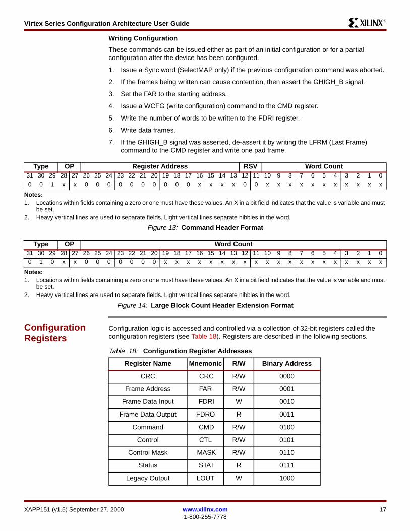
Virtex Series Configuration Architecture User GuideR13
Writing Configuration
These commands can be issued either as part of an initial configuration or for a partialconfiguration after the device has been configured
1 Issue a Sync word (SelectMAP only) if the previous configuration command was aborted
2 If the frames being written can cause contention then assert the GHIGH_B signal
3 Set the FAR to the starting address
4 Issue a WCFG (write configuration) command to the CMD register
5 Write the number of words to be written to the FDRI register
6 Write data frames
7 If the GHIGH_B signal was asserted de-assert it by writing the LFRM (Last Frame)command to the CMD register and write one pad frame
ConfigurationRegisters
Configuration logic is accessed and controlled via a collection of 32-bit registers called theconfiguration registers (see Table 18) Registers are described in the following sections
Type OP Register Address RSV Word Count31 30 29 28 27 26 25 24 23 22 21 20 19 18 17 16 15 14 13 12 11 10 9 8 7 6 5 4 3 2 1 00 0 1 x x 0 0 0 0 0 0 0 0 0 0 x x x x 0 0 x x x x x x x x x x x
Notes1 Locations within fields containing a zero or one must have these values An X in a bit field indicates that the value is variable and must
be set2 Heavy vertical lines are used to separate fields Light vertical lines separate nibbles in the word
Figure 13 Command Header Format
Type OP Word Count31 30 29 28 27 26 25 24 23 22 21 20 19 18 17 16 15 14 13 12 11 10 9 8 7 6 5 4 3 2 1 00 1 0 x x 0 0 0 0 0 0 0 x x x x x x x x x x x x x x x x x x x x
Notes1 Locations within fields containing a zero or one must have these values An X in a bit field indicates that the value is variable and must
be set2 Heavy vertical lines are used to separate fields Light vertical lines separate nibbles in the word
Figure 14 Large Block Count Header Extension Format
Table 18 Configuration Register Addresses
Register Name Mnemonic RW Binary Address
CRC CRC RW 0000
Frame Address FAR RW 0001
Frame Data Input FDRI W 0010
Frame Data Output FDRO R 0011
Command CMD RW 0100
Control CTL RW 0101
Control Mask MASK RW 0110
Status STAT R 0111
Legacy Output LOUT W 1000
XAPP151 (v15) September 27 2000 wwwxilinxcom 171-800-255-7778
Virtex Series Configuration Architecture User GuideR13
Command Register (CMD)The content of the Command Register (CMD) is interpreted by the configuration state machineConfiguration commands control the operation of the configuration state machine the FrameData Register (FDR) and some of the global signals The command in the Command Registeris executed each time the FAR is loaded with a new value The effect of each command isdefined in Table 19
Configuration Option COR RW 1001
Reserved mdash mdash 1010
Frame Length FLR RW 1011
Reserved mdash mdash 1100
Reserved mdash mdash 1101
Reserved mdash mdash 1110
Reserved mdash mdash 1111
Table 18 Configuration Register Addresses (Continued)
Register Name Mnemonic RW Binary Address
Table 19 Configuration Commands
Cmd Code Description
Rsvd 0000 Reserved
WCFG 0001Write Configuration Data mdash Used prior to writing configuration data to the FDRI It takes theinternal configuration state machine through a sequence of states that control the shifting of the FDRand the writing of the configuration memory (See Frame Data Input Register (FDRI) on page 24)
Rsvd 0010 Reserved
LFRM 0011Last Frame mdash This command is loaded prior to writing the last (pad) data frame if the GHIGH_Bsignal was asserted This command is not necessary if the GHIGH_B signal was not asserted Thisallows overlap of the last frame write with the release of the GHIGH_B signal
RCFG 0100Read Configuration Data mdash Used prior to reading frame data from the FDRO Similar to the WCFGcommand in its effect on the FDR (see Frame Data Output Register (FDRO) on page 24)
START 0101Begin Startup Sequence mdash Starts the startup sequence This command is also used to start ashutdown sequence prior to partial re-configuration The Startup Sequence begins with the nextsuccessful CRC check (see Cyclic Redundancy Check (CRC) on page 22)
RCAP 0110Reset Capture mdash Used when performing capture in single-shot mode This command must be usedto reset the capture signal if single-shot capture has been selected
RCRC 0111 Reset CRC mdash Used to reset CRC register (see Cyclic Redundancy Check (CRC) on page 22)
AGHIGH 1000Assert GHIGH_B Signal mdash Used prior to re-configuration to prevent contention while writing newconfiguration data All CLB outputs and signals are forced to a one
SWITCH 1001Switch CCLK Frequency mdash Used to change (increase) the frequency of the Master CCLK Thenew frequency is specified in Table 21
Rsvd 1010 Reserved
Rsvd 1011 Reserved
Rsvd 1100 Reserved
18 wwwxilinxcom XAPP151 (v15) September 27 20001-800-255-7778
Virtex Series Configuration Architecture User GuideR13
Configuration Option Register (COR)The Configuration Option Register (COR) is used to select configuration options that areillustrated in Figure 15 and defined in Table 20 Entries in this table are further explained in thefollowing tables
Rsvd 1101 Reserved
Rsvd 1110 Reserved
Rsvd 1111 Reserved
Table 19 Configuration Commands (Continued)
Cmd Code Description
DO
NE
_PIP
E
DR
IVE
_DO
NE
SIN
GLE
OS
CF
SE
L
SS
CLK
SR
C
LOC
K_W
AIT
SH
UT
DO
WN
DO
NE
_CY
CLE
LCK
_CY
CLE
GT
S_C
YC
LE
GW
E_C
YC
LE
GS
R_C
YC
LE
31 30 29 28 27 26 25 24 23 22 21 20 19 18 17 16 15 14 13 12 11 10 9 8 7 6 5 4 3 2 1 00 x x x x x x x x x x x x x x x x x x x x x x x x x x x x x x x
Notes1 Locations within fields containing a zero or one must have these values An X in a bit field indicates that the value is variable and must
be set2 Heavy vertical lines are used to separate fields Light vertical lines separate nibbles in the word
Figure 15 COR (Configuration of Option Register) Fields
XAPP151 (v15) September 27 2000 wwwxilinxcom 191-800-255-7778
Virtex Series Configuration Architecture User GuideR13
Table 21 shows the allowed values for the OSCFSEL field of the COR Setting OSCFSEL toone of these values will set the Master CCLK frequency to the specified value
Table 20 Configuration Option Register Fields
Field Bit Indices DescriptionBitgenDefault
DONE_PIPE 30
0 No pipeline stage for DONEIN
1 Add pipeline stage to DONEINFPGA waits on DONE that is delayed by one (1) cycle of the StartupClkrather than the pin itself Use this option when StartupClk is running at highspeeds
0
DRIVE_DONE 290 DONE pin is open drain
1 DONE pin is actively driven high0
SINGLE 28 Readback capture is one-shot 0
OSCFSEL 2722 Select CCLK frequency in Master Serial configuration mode 2
SSCLKSRC 2120
Startup sequence clock source00 Cclk01 UserClk1x JTAGClk
0
LOCK_WAIT 1916
4-bit mask indicating which DLL lock signals to wait for during LCK cycleThe 4 bits (from MSB to LSB) correspond to DLLs TL=3 TR=2 BL=1BR=0 (top-left top-right etc) In Virtex-E devices where there are 8 DLLseach mask bit applies to the 2 DLLs in that quadrant of the device Thedefault is not to wait for any DLL lock signals
0
SHUTDOWN 15
Indicate whether doing a startup or shutdown sequence
0 Startup
1 Shutdown sequence
0
DONE_CYCLE 1412 Startup phase in which DONE pin is released 3
LCK_CYCLE 119 Stall in this startup phase until DLL locks are asserted 7
GTS_CYCLE 86 Startup phase in which IOs switch from tri-state to user design 4
GWE_CYCLE 53 Startup phase in which the global write-enable is asserted 5
GSR_CYCLE 20 Startup phase in which the global setreset is negated 5
Table 21 OSCFSEL-Specified Master CCLK Frequencies)
CCLK(MHz) OSCFSEL
CCLK(MHz) OSCFSEL
CCLK(MHz) OSCFSEL
43 000010 13 001010 41 100111
54 010001 15 001101 45 110011
69 000100 20 010111 51 101010
81 000101 26 011010 55 110100
20 wwwxilinxcom XAPP151 (v15) September 27 20001-800-255-7778
Virtex Series Configuration Architecture User GuideR13
Table 22 shows the values of the DONE_CYCLE LCK_CYCLE GTS_CYCLE GWE_CYCLEand GSR_CYCLE fields in COR This table shows the step in the start-up sequence when eachof these signals becomes active
Control Register (CTL)The Control Register (CTL) fields are illustrated in Figure 16 on page 21 and defined inTable 23
92 000110 30 011101 60 101101
100 000111 34 110010 mdash mdash
Notes1 These values are accurate to +45 ndash 30
Table 22 COR Startup Cycle Fields
FieldValue
DONE_CYCLE(DONE Active)
GTS_CYCLE(GTS_CFGInactive)
GSR_CYCLE(GSR Inactive)
GWE_CYCLE(GWE Active) LCK_CYCLE
000 1 1 1 1 0
001 2 2 2 2 1
010 3 3 3 3 2
011 4 (default) 4 4 4 3
100 5 5 (default) 5 5 4
101 6 6 6 (default) 6 (default) 5
110 mdash DoneIndagger DoneIndagger DoneIndagger 6
111 Keep State Keep State Keep State Keep State Donrsquot Wait(default)
Notes1 dagger DONE if DonePipe = No else the delayed version of DONE
Table 21 OSCFSEL-Specified Master CCLK Frequencies) (Continued)
CCLK(MHz) OSCFSEL
CCLK(MHz) OSCFSEL
CCLK(MHz) OSCFSEL
SB
ITS
PE
RS
IST
GT
S_U
SR
_B
31 30 29 28 27 26 25 24 23 22 21 20 19 18 17 16 15 14 13 12 11 10 9 8 7 6 5 4 3 2 1 00 0 0 0 0 0 0 0 0 0 0 0 0 0 0 0 0 0 0 0 0 0 0 x x x 0 0 0 0 0 x
Notes1 Locations within fields containing a zero or one must have these values An X in a bit field indicates that the value is variable and must
be set2 Heavy vertical lines are used to separate fields Light vertical lines separate nibbles in the word
Figure 16 Control Register Fields
XAPP151 (v15) September 27 2000 wwwxilinxcom 211-800-255-7778
Virtex Series Configuration Architecture User GuideR13
Cyclic Redundancy Check (CRC)A data input error checking mechanism is provided through the Cyclic Redundancy Check(CRC) register When data is written to any configuration register (except LOUT) a 16-bit CRCvalue is calculated using both the register data and the address This value is saved in the CRCregister At the end of any series of writes a pre-calculated CRC block-check value may bewritten to the CRC register If the resulting value is non-zero an error is indicated TheCRC_ERROR bit is accessible through the status register If a CRC error is detectedconfiguration logic is put in the ERROR mode The following section is an algorithm forcomputing CRC
CRC Algorithm Initialization bcc = 0skip_pad = truemore_words = true Check for write operation do
w = next_wordif (w[3127] == rsquo00101rsquo)
A Read OP Donrsquot use in CRCwc = w[100]if (wc == 0)
w = next_wordwc = w[190]
while (wc-- gt 0)
w = next_word
elsif (w[3127] == rsquo00110rsquo)
A Write OP Use in CRC addr = w[1613]if (addr Π0124569DB)
wc = w[100]if (wc == 0)
wc is in next word w = next_wordwc = w[190]
while (wc-- gt 0)
w = next_wordsw[350] = addr wordfor (i=0 ilt36 i++)
Table 23 Control Register Bits
NameBit
Indices Description
SBITS 87 Security level0 ReadWrite OK (default)1 Readback disabled23 Readback disabled Writing disabled except CRCregister
PERSIST 6 Configuration interface remains after configuration0 No (default)1 Yes
GTS_USR_B 0 Active-low global tristate IOs Turn off pull-ups ifGTS_CFG_B is also asserted
22 wwwxilinxcom XAPP151 (v15) September 27 20001-800-255-7778
Virtex Series Configuration Architecture User GuideR13
x16 = bcc[15] XOR sw[i]x15 = bcc[14] XOR x16x2 = bcc[1] XOR x16bcc[150] =
x15bcc[132]x2bcc[0]x16 Note the bit order crc[150] = bcc[015]
else
Pad word - ignore
while (more_words)
Frame Address Register (FAR)The Frame Address Register (FAR) holds the address of the current frame The address isdivided into three parts the block type the major address and the minor address The blocktype field indicates whether the CLB or block RAM address space is used The command in thecommand register is executed each time the FAR is loaded with a new value
The major address selects the CLB or RAM column the minor address selects the frame withinthe column The minor address is incremented each time a full data frame is read from orwritten to the frame data register If the last frame within the CLB column is selected when theincrement occurs the major address is incremented and the minor address is reset to zerootherwise the minor address is incremented However the block RAM major address is notincremented automatically
See Figure 18 for the definitions of valid values for the block type field The FAR field definitionsare shown in Figure 19
Figure 17 CRC Calculation Register
Note the Block RAM Major Address is not incremented automatically To address a differentBlock RAM Content column the FAR must be loaded with the new Major Address
Type CodesCLB 00RAM 01
Figure 18 Block Type Codes
x151_17_021100
15141312111098765432
1013
01234526272829303101
Address 32-bit Data Word
CRC Calculation Register
CRC Data Input Register
CRC Register [310]
DATA_IN
SHIFT
23
16-bit CRC13150
0000 0000 0000 0000133116
1313
XAPP151 (v15) September 27 2000 wwwxilinxcom 231-800-255-7778
Virtex Series Configuration Architecture User GuideR13
Frame Data Input Register (FDRI)The Frame Data Input Register (FDRI) is used to load configuration frame data into a Virtexdevice
The Frame Data Register (FDR) is a shift register into which data is loaded prior to transfer tothe configuration memory Configuration data is written to the Virtex device by loading thecommand register with the WCFG command and then loading the FDR with at least two framesof 32-bit words
The write operation is pipelined such that the first frame of data is written to the configurationmemory while the second frame is being shifted in The last frame (the pad frame) is alwaysdummy data which is not actually written to the configuration memory Each frame write mustinclude enough 32 bit data words to load the frame fully There is one pad word at the end ofeach frame which is required for the pipelining hardware
Frame Data Output Register (FDRO)The Frame Data Output Register (FDRO) is for reading configuration data or captured datafrom the Virtex device a process called readback Readback is performed by loading thecommand register with the RCFG command and then addressing the FDRO with a readcommand
Frame Length Register (FLR)Near the beginning of the configuration bitstream the Frame Length Register (FLR) is writtenwith the length of a frame as measured in 32-bit words This length count is used to providesequencing information for the configuration read and write operations Note that the FLR mustbe written before any FDR operation works It is not necessary to set the FLR more than onceIf the number of bits in a frame is not evenly divisible by 32 the length count of the frame mustbe rounded up to the next highest integer The values for the FLR for all the current Virtexseries devices are given in Table 24
BlockType
Major Address(Column Address)
Minor Address(Frame Address)
31 30 29 28 27 26 25 24 23 22 21 20 19 18 17 16 15 14 13 12 11 10 9 8 7 6 5 4 3 2 1 00 0 0 0 0 x x x x x x x x x x x x x x x x x x 0 0 0 0 0 0 0 0 0
Notes1 Locations within fields containing a zero or one must have these values An X in a bit field indicates that the value is variable and must
be set2 Heavy vertical lines are used to separate fields Light vertical lines separate nibbles in the word
Figure 19 Frame Address Fields (FAR)
Note The FLR contains a value that is one less than the number of words that are read fromor written to a given frame This is because the extra word needed for pipelining is not counted
Table 24 Frame Length Register Value
Device Row times Col Frame Length Words per Frame FLR Value
XCV50E 16 times 24 384 12 11
XCV100E 20 times 30 448 14 13
XCV150 24 times 36 512 16 15
XCV200E 28 times 42 576 18 17
XCV300E 32 times 48 672 21 20
24 wwwxilinxcom XAPP151 (v15) September 27 20001-800-255-7778
Virtex Series Configuration Architecture User GuideR13
Legacy Output Register (LOUT)The Legacy Output Register (LOUT) is used for daisy chaining the configuration bitstream toother Xilinx devices Data written to the LOUT is serialized and appears on the DOUT pin
Mask Register (MASK)The Mask Register (MASK) is a mask register for writes to the CTL register A 1 in bit N of themask allows that bit position to be written in the CTL register The default value of the mask isall 0s
Status Register (STAT)The Status Register (STAT) is loaded with current values of several control or status signalsThe register can be read via the re-configuration block or via JTAG The fields in the Statusregister are illustrated in Figure 20 The values of the signals given in Table 25 on page 26 canbe read from the status register
XCV400E 40 times 60 800 25 24
XCV405E 40 times 60 800 25 24
XCV600E 48 times 72 960 30 29
XCV800 56 times 84 1088 34 33
XCV812E 56 times 84 1088 34 33
XCV1000E 64 times 96 1248 39 38
XCV1600E 72 times 108 1376 43 42
XCV2000E 80 times 120 1536 48 47
XCV2600E 92 times 138 1728 54 53
XCV3200E 104 times 156 1952 61 60
Table 24 Frame Length Register Value (Continued)
Device Row times Col Frame Length Words per Frame FLR Value
DO
NE
INIT
MO
DE
GH
IGH
_B
GS
R_B
GW
E_B
GT
S_C
FG
IN_E
RR
OR
LOC
K
CR
C_E
RR
OR
31 30 29 28 27 26 25 24 23 22 21 20 19 18 17 16 15 14 13 12 11 10 9 8 7 6 5 4 3 2 1 00 0 0 0 0 0 0 0 0 0 0 0 0 0 0 0 0 x x x x x x x x x x x x x x x
Notes1 An X in a bit field indicates that the value is variable2 Heavy vertical lines are used to separate fields Light vertical lines separate nibbles in the word
Figure 20 Status Register Fields
XAPP151 (v15) September 27 2000 wwwxilinxcom 251-800-255-7778
Virtex Series Configuration Architecture User GuideR13
ConfigurationInterface
There are two configuration interfaces to the Virtex devices mdash the bit-serial Boundary Scaninterface and the 8-bit byte-serial SelectMAP interface Conceptually XCV50 configurationdata appears as in Figure 21
Frames and words within frames are written in the same order in both configuration interfacesstarting with Frame 0 word 0 (the left-most in the picture) followed by word 1 etc Bits withineach word are written from left to right (MSB first) in the bit-serial configuration interfaces
Within the SelectMAP interface data is written a byte at a time A sample word is shown inFigure 22 The top row indicates the device pin names The bottom row indicates the bit indiceswithin a configuration word Byte 0 loads first followed by byte 1 et cetera The MSB of eachbyte (ie bits 31 23 15 and 7) is loaded on pin D0 The LSB of each byte (ie bits 24 16 8and 0) is loaded on pin D7
PartialReconfigurationof CLBs
Partial reconfiguration can be performed with and without shutting down the device Ifcontention occurs it is advised to go through a shutdown sequence prior to loadingconfiguration frames When shutting down the DONE pin will go active and pull low If this is notdesireable the DONE pin can be prevented from going low by selecting the DONE_CYCLE toKeep State (111) Similarly to prevent GSR from becoming active and reseting the currentstate the GSR_CYCLE can be set to Keep State When not shutting down changes occurframe by frame but is completely done by the end of the Last Frame packet (see Example 1)
Table 25 Status Register Bits
Name Bit Indices Description
DONE 14 Input from DONE pin
INIT 13 Value of INIT
MODE 1210 Value of M2 M1 M0 mode pins
GHIGH_B 9 0 = GHIGH_B asserted
GSR_B 8 0 = all flip-flops are ResetSet
GWE_B 7 1 = flip-flops and block RAM are write disabled
GTS_CFG 6 0 = IOs are tri-stated
IN_ERROR 5 Legacy input error
LOCK 41 Output from DLL lock signals 1 = DLL is locked
CRC_ERROR 0 Indicates that a CRC error has occurred
Data Frame 0 (11 words) Pad Word
hellip
Data Frame n (11 words) Pad WordPad Frame (12 words)
Figure 21 XCV50 Frame Padding for Reads
Figure 22 SelectMAP Byte and Bit Ordering
x151_22_021100
D0 D1 D2 D3 D4 D5 D6 D7 D0 D1 D2 D3 D4 D5 D6 D7 D0 D1 D2 D3 D4 D5 D6 D7 D0 D1 D2 D3 D4 D5 D6 D7
Byte 0 Byte 1 Byte 2 Byte 313
26 wwwxilinxcom XAPP151 (v15) September 27 20001-800-255-7778
Virtex Series Configuration Architecture User GuideR13
The DONE pin will not change in this case Figure 23 illustrates a typical shutdownreconfiguration in the CLB address space and restart sequence
Examples Several examples of reading and evaluating configuration data are provided to illustrate thefollowing
Figure 23 Typical Shutdown Reconfiguration in the CLB Address Spaceand Restart Sequence
FFFF FFFF Dummy WordAA99 5566 Sync Word Does not realign an already synchronized SelectMap port3001 2001 COR0080 FF2F Shutdown bit set optionally set bit 29 DRIVE_DONE
Alternately COR may be read bit 15 set and written back3000 8001 CMD0000 0005 Start Shutdown3000 8001 CMD0000 0007 Reset CRC0000 00000000 0000 Clock shutdown sequence0000 00000000 00003000 8001 CMD0000 0008 Assert GHIGH3000 8001 CMD0000 0001 Write Configuration3000 2001 FAR0--- ---- Block Type CLB (00) MajorMinor Address3000 4--- FDRI + Word Count if count is lt1024 Otherwise use TypeII Header
Write FRAME DATAIf CLB Frames are not written to non-consecutive addresses repeat FAR word followedby new MajorMinor Address followed by FDRI + Word Count and then Frame Data
3000 0001 Write CRC---- ---- CRC3000 8001 CMD0000 0003 LFRM3000 4--- FDRI + Word Count
Write PAD FRAME
3001 2001 COR0080 3F2D Default COR Options
Alternately COR may be read bit 15 cleared and written back3000 8001 CMD0000 0005 Begin Startup3000 0001 Write CRC---- ---- CRC
0000 00000000 0000 4 Dummy Words0000 00000000 0000
Example 1 Read and Write Semaphores in an XCV100 at CLB R1 C1 Slice 0 on page 28Example 2 Reading the Complete Configuration from an XCV50 on page 33
XAPP151 (v15) September 27 2000 wwwxilinxcom 271-800-255-7778
Virtex Series Configuration Architecture User GuideR13
Example 1 Read and Write Semaphores in an XCV100 at CLB R1 C1Slice 0Semaphores are a useful communication mechanism documented in XAPP 153 ldquoStatus andControl Semaphore Registers using Partial Reconfigurationrdquo Figure 24 shows an abstractionof a microprocessor writing control information to an FPGA and reading status informationOne convention for implementing semaphores in Virtex devices is to use two bits of a 16-bitdual-port RAM as illustrated in Figure 25 This occupies one CLB slice with the F-LUTimplementing the control semaphore and the status semaphore implemented in the G-LUTAddress 15 of the G-LUT is used for on-chip writes to the semaphore and address 14 of the F-LUT is used for on-chip reads Conversely the off-chip microprocessor is reading the G-LUT[15] and writing F-LUT[14]
Example 3 Read the Slice 0 G-LUT from CLB R1 C1 from the Complete Configuration of anXCV50 on page 34Example 4 Read the Slice 1 F-LUT from CLB R19 C16 from an XCV100 on page 36Example 5 Read All Bits in Slice 0 G-LUTs from CLB C2 and XCV50 on page 39Example 6 Read Block SelectRAM index 387 of RAM R2 C0 from an XCV100E on page 41
Figure 24 Semaphore Abstraction
x151_ 23_021400
Status13
Control13
MicroProcessor FPGA13
Semaphores13
28 wwwxilinxcom XAPP151 (v15) September 27 20001-800-255-7778
Virtex Series Configuration Architecture User GuideR13
Using a Semaphore Abstraction dual-port RAM ensures that the LUT SelectRAMs are placedin the CLB in a predictable manner When writing data to one or more LUT SelectRAMs or flip-flops on the device all bits in the frame must have valid configuration information This isassured by altering valid configurations from bitstream files or from frames read from a properlyconfigured Virtex device The latter approach is used in this example
Figure 25 Semaphore ReadWrite Implementation
Frame 47
15
14
47 46
47 46
x151_ 24_021100
Select Map
Frame 46
DING
F
13
D2D3D4 5D6 7D0D1 D D
1
111
0
111
Chip Interface
G F
13
XAPP151 (v15) September 27 2000 wwwxilinxcom 291-800-255-7778
Virtex Series Configuration Architecture User GuideR13
Attributes for this design are summarized in Table 26
From the equations in Table 7 on page 11 the values shown in Table 27 can be calculated
From off-chip for reading the G-LUT[15] bit read one frame (MNA=47) For writing the F-LUT[14] bit we show how to read then write one frame (MNA=46) as opposed to modifyingdata from a bitstream file (both are valid methods) The frames on the XCV100 contain 13 32-bit words and one pad word Remember that fm_st_wd is calculated assuming the entireconfiguration has been read However only the pad frame and then frames 46 and 47 fromMajor Address 30 are being read The desired bit is in Frame 1 word 1 which is word 15
The commands for reading both frames (and the pad frame) are given in Figure 26
Table 26 Design Attributes for Example 1
Attribute
G-LUT [15] F-LUT [14]
Read Read Write
Chip_Rows 20
Chip_Cols 30
FL 14
CLB_Row 1
CLB_Col 1
Slice 0
FG 1 0
lut_bit 15 14
RW 1 1 0
Table 27 Semaphore Example Variables Equations and Values
Variable Equation
Value(s)
G-LUT[15] F-LUT[14]
Read Read Write
MJA 1 le 302 rArr 30 ndash 1 times 2 + 2 30
MNA lut_bit + 32ndash 0 times () 47 46
fm_bit_idx 3 + 18 times 1 ndash FG + RW times 32 52 53 21
fm_st_wd 14 times (8 + (30 ndash 1) times 48+ 4647) +RW times (14 +1)= 14 times (1400 + 4647) + 14 times RW= 19600 + 14 times 4647 + 14 times RW
20272 20258 20244
fm_wd floor (2032) 1 1 0
fm_wd_bit_idx 31 + 32 times 110 ndash 525321 11 10 10
30 wwwxilinxcom XAPP151 (v15) September 27 20001-800-255-7778
Virtex Series Configuration Architecture User GuideR13
The 42 words read are shown in Figure 27 F-LUT[14] is in the second frame (frame=1word=1) at bit 10 The value read is a 1 but because the LUT bits are inverted the logic valueis zero G-LUT[15] is in word one of the third data frame (frame=2 word=1) at bit 11The valueread is a 1 which is a logic zero
InstructionData
Hex 31 30 29 28 27 26 25 24 23 22 21 20 19 18 17 16 15 14 13 12 11 10 9 8 7 6 5 4 3 2 1 0
Sync Word AA99 5566 1 0 1 0 1 0 1 0 1 0 0 1 1 0 0 1 0 1 0 1 0 1 0 1 0 1 1 0 0 1 1 0
Write next (1) word to FAR 3000 2001 0 0 1 1 0 0 0 0 0 0 0 0 0 0 0 0 0 0 1 0 0 0 0 0 0 0 0 0 0 0 0 1
CLB MJA=30 MNA=46 003C 5800 0 0 0 0 0 0 0 0 0 0 1 1 1 1 0 0 0 1 0 1 1 1 0 0 0 0 0 0 0 0 0 0
Write next word to CMD 3000 8001 0 0 1 1 0 0 0 0 0 0 0 0 0 0 0 0 1 0 0 0 0 0 0 0 0 0 0 0 0 0 0 1
Register value for RCFG 0000 0004 0 0 0 0 0 0 0 0 0 0 0 0 0 0 0 0 0 0 0 0 0 0 0 0 0 0 0 0 0 1 0 0
Read from FDRO 2800 602A 0 0 1 0 1 0 0 0 0 0 0 0 0 0 0 0 0 1 1 0 0 0 0 0 0 0 1 0 1 0 1 0
Flush pipe 0000 0000 0 0 0 0 0 0 0 0 0 0 0 0 0 0 0 0 0 0 0 0 0 0 0 0 0 0 0 0 0 0 0 0
(read 42 words)
Notes1 Binary data is grouped in two ways for ease of interpretation Thin vertical lines separate nibble boundaries Heavy vertical lines
separate field boundaries
Figure 26 Commands to Read Two Data Frames
XAPP151 (v15) September 27 2000 wwwxilinxcom 311-800-255-7778
Virtex Series Configuration Architecture User GuideR13
To write to the F-LUT semaphore start with the second data frame (frame=1) that was justread Words 1 - 13 of that frame will become words 0 - 12 of the frame to be written Word 13of this new frame is a pad word and can have any value (typically 0 is chosen) In this newframe set bit 11 of word 0 (zero) to the desired value of the semaphore A pad frame mustfollow the data frame The commands from Figure 28 write these two frames into the device atthe proper location
Frame Word 31 30 29 28 27 26 25 24 23 22 21 20 19 18 17 16 15 14 13 12 11 10 9 8 7 6 5 4 3 2 1 0
0
0 1 1 1 1 1 1 1 1 1 1 1 1 1 1 1 1 1 1 1 1 1 1 1 1 1 1 1 1 1 1 1 1
1 1 1 1 1 1 1 1 1 1 1 1 1 1 1 1 1 1 1 1 1 1 1 1 1 1 1 1 1 1 1 1 1
2 1 1 1 1 1 1 1 1 1 1 1 1 1 1 1 1 1 1 1 1 1 1 1 1 1 1 1 1 1 1 1 1
3 1 1 1 1 1 1 1 1 1 1 1 1 1 1 1 1 1 1 1 1 1 1 1 1 1 1 1 1 1 1 1 1
4 1 1 1 1 1 1 1 1 1 1 1 1 1 1 1 1 1 1 1 1 1 1 1 1 1 1 1 1 1 1 1 1
5 1 1 1 1 1 1 1 1 1 1 1 1 1 1 1 1 1 1 1 1 1 1 1 1 1 1 1 1 1 1 1 1
6 1 1 1 1 1 1 1 1 1 1 1 1 1 1 1 1 1 1 1 1 1 1 1 1 1 1 1 1 1 1 1 1
7 1 1 1 1 1 1 1 1 1 1 1 1 1 1 1 1 1 1 1 1 1 1 1 1 1 1 1 1 1 1 1 1
8 1 1 1 1 1 1 1 1 1 1 1 1 1 1 1 1 1 1 1 1 1 1 1 1 1 1 1 1 1 1 1 1
9 1 1 1 1 1 1 1 1 1 1 1 1 1 1 1 1 1 1 1 1 1 1 1 1 1 1 1 1 1 1 1 1
10 1 1 1 1 1 1 1 1 1 1 1 1 1 1 1 1 1 1 1 1 1 1 1 1 1 1 1 1 1 1 1 1
11 1 1 1 1 1 1 1 1 1 1 1 1 1 1 1 1 1 1 1 1 1 1 1 1 1 1 1 1 1 1 1 1
12 1 1 1 1 1 1 1 1 1 1 1 1 1 1 1 1 1 1 1 1 1 1 1 1 1 1 1 1 1 1 1 1
13 1 1 1 1 1 1 1 1 1 1 1 1 1 1 1 1 1 1 1 1 1 1 1 1 1 1 1 1 1 1 1 1
1
0 0 0 0 0 0 0 0 0 0 0 0 0 0 0 0 0 0 0 0 0 0 0 0 0 0 0 0 0 0 0 0 0
1 1 0 0 0 0 0 0 0 0 0 0 0 1 0 0 0 0 1 1 0 1 1 0 0 0 0 0 0 0 0 0 0 F[14]
2 1 1 1 1 1 0 1 1 0 0 0 0 1 1 1 1 0 0 1 1 1 1 1 0 1 1 0 0 0 0 0 0
3 0 0 0 0 1 1 1 1 1 0 1 1 0 0 0 0 0 0 0 0 0 0 1 1 1 1 1 0 1 1 0 0
4 0 0 0 0 0 0 0 0 1 1 1 1 0 0 0 0 0 0 0 0 0 0 0 0 0 0 1 1 1 1 1 0
5 1 1 0 0 1 1 0 0 0 0 0 0 1 1 0 0 1 0 1 1 0 0 0 0 0 0 0 0 0 0 1 1
6 1 1 1 0 1 1 0 0 0 0 0 0 1 1 1 0 1 1 1 0 1 0 1 1 0 0 0 0 0 0 0 0
7 0 0 1 1 1 1 1 0 1 1 0 0 0 0 1 1 0 0 0 0 1 1 1 1 1 0 1 1 0 0 0 0
8 0 0 0 0 0 0 1 1 1 1 1 0 0 0 0 0 0 0 0 0 0 0 0 0 1 1 1 1 1 0 1 1
9 0 0 0 0 0 0 0 0 0 0 1 1 0 0 0 0 1 1 0 0 0 0 0 0 0 0 0 0 1 1 1 1
10 1 0 1 1 0 0 0 0 0 0 0 0 1 0 1 1 1 1 1 0 1 1 0 0 0 0 0 0 0 0 0 0
11 1 1 1 1 1 0 1 1 0 0 0 0 1 1 1 1 0 0 1 1 1 1 1 0 1 1 0 0 0 0 0 0
12 0 0 0 0 1 1 0 1 1 0 1 1 0 0 0 0 0 0 0 0 0 0 1 1 1 1 1 0 0 0 0 0
13 0 0 0 0 0 0 1 1 0 1 0 1 0 0 0 0 0 0 0 0 0 0 0 0 0 0 0 0 0 0 0 0
2
0 0 0 0 0 0 0 0 0 0 0 0 0 0 0 0 0 0 0 0 0 0 0 0 0 0 0 0 0 0 0 0 0
1 1 0 1 0 0 0 0 0 0 0 0 1 1 0 1 0 1 1 1 0 1 1 0 0 0 0 0 0 0 0 0 0 G[15]
2 1 1 1 1 1 1 1 1 0 0 0 0 1 1 1 1 0 0 1 1 1 1 1 1 1 1 0 0 0 0 0 0
3 0 0 0 0 1 1 1 1 1 1 1 1 0 0 0 0 0 0 0 0 0 0 1 0 1 1 1 1 1 1 0 0
4 0 0 0 0 0 0 0 0 1 1 1 1 0 0 0 0 0 0 0 0 0 0 0 0 0 0 1 1 1 1 1 1
5 1 1 0 0 0 0 0 0 0 0 0 0 1 1 0 0 1 1 1 1 0 0 1 0 0 0 0 0 0 0 1 1
6 1 1 1 1 1 1 0 0 0 0 0 0 1 1 1 1 1 1 1 1 1 1 1 1 0 0 0 0 0 0 0 0
7 0 0 1 1 1 1 1 1 1 1 0 0 0 0 1 1 0 0 0 0 1 1 1 1 1 1 1 1 0 0 0 0
8 0 0 0 0 0 0 1 1 1 1 1 1 0 0 0 0 0 0 0 0 0 0 0 0 1 1 1 1 1 1 1 1
9 0 0 0 0 0 0 0 0 0 0 1 1 0 0 0 0 1 1 0 0 0 0 0 0 0 0 0 0 1 1 1 1
10 1 1 1 1 0 0 0 0 0 0 0 0 1 1 1 1 1 1 1 1 1 1 0 0 0 0 0 0 0 0 0 0
11 1 1 1 1 1 1 1 1 0 0 0 0 1 1 1 1 0 0 1 1 1 1 1 1 1 1 0 0 0 0 0 0
12 0 0 0 0 1 1 0 1 1 1 1 1 0 0 0 0 0 0 0 0 0 0 1 1 1 1 1 0 1 0 0 0
13 0 0 0 0 0 1 1 0 0 1 1 1 0 0 0 0 0 0 0 0 0 0 0 0 0 0 0 0 0 0 0 0
Figure 27 Three Frames Containing the Semaphores
32 wwwxilinxcom XAPP151 (v15) September 27 20001-800-255-7778
Virtex Series Configuration Architecture User GuideR13
Example 2 Reading the Complete Configuration from an XCV50Steps
1 If flip-flop values are needed clock the on-chip signal CAPTURE to capture flip-flopvalues See the Xilinx Libraries Guide for use of the CAPTURE_VIRTEX cell
2 Write the starting frame address (CLB MJA=0 MNA=0) into the FAR
3 Write the RCFG command to the CMD register
4 Address the FDRO register with a READ operation and word count equal to the number of32-bit words in the CLB frames plus one pad frame
5 Read the data following the timing diagrams in the SelectMAP interface section
6 Write the address for RAM block 0 to the FAR
7 Address the FDRO register with a read operation and word count equal to the number of32-bit words in the RAM block plus one pad frame
8 Read the data
9 Write the address for RAM block 1 to the FAR
10 Address the FDRO register with a read operation and word count equal to the number of32-bit words in the RAM block plus one pad frame
11 Read the data
When using SelectMAP mode to read data words from the Virtex device de-assert CS de-assert WRITE assert CS then clock the data out When using JTAG load the JTAG IR
InstructionData
Hex 31 30 29 28 27 26 25 24 23 22 21 20 19 18 17 16 15 14 13 12 11 10 9 8 7 6 5 4 3 2 1 0
Sync Word AA995566
1 0 1 0 1 0 1 0 1 0 0 1 1 0 0 1 0 1 0 1 0 1 0 1 0 1 1 0 0 1 1 0
Write next (1) word to FAR 30002001
0 0 1 1 0 0 0 0 0 0 0 0 0 0 0 0 0 0 1 0 0 0 0 0 0 0 0 0 0 0 0 1
MJA=30 MNA=46 003C5C00
0 0 0 0 0 0 0 0 0 0 1 1 1 1 0 0 0 1 0 1 1 1 0 0 0 0 0 0 0 0 0 0
Write next word to CMD 30008001
0 0 1 1 0 0 0 0 0 0 0 0 0 0 0 0 1 0 0 0 0 0 0 0 0 0 0 0 0 0 0 1
Register value for WCFG 00000001
0 0 0 0 0 0 0 0 0 0 0 0 0 0 0 0 0 0 0 0 0 0 0 0 0 0 0 0 0 0 0 1
Write 28 words to FDRI 3000401C
0 0 1 1 0 0 0 0 0 0 0 0 0 0 0 0 0 1 0 0 0 0 0 0 0 0 0 1 1 1 0 0
Data Word 0 A01AEC00
1 0 1 0 0 0 0 0 0 0 0 1 1 0 1 0 1 1 1 0 1 1 0 0 0 0 0 0 0 0 0 0
Data Word 1 FF0F3FC0
1 1 1 1 1 1 1 1 0 0 0 0 1 1 1 1 0 0 1 1 1 1 1 1 1 1 0 0 0 0 0 0
Data Word 2 0FF002FC
0 0 0 0 1 1 1 1 1 1 1 1 0 0 0 0 0 0 0 0 0 0 1 0 1 1 1 1 1 1 0 0
hellip hellip hellip
Data Word 27 00000000
0 0 0 0 0 0 0 0 0 0 0 0 0 0 0 0 0 0 0 0 0 0 0 0 0 0 0 0 0 0 0 0
Notes1 Binary data is grouped in two ways for ease of interpretation Thin vertical lines separate nibble boundaries Heavy
vertical lines separate field boundaries
Figure 28 Commands to Write a Semaphore Value
XAPP151 (v15) September 27 2000 wwwxilinxcom 331-800-255-7778
Virtex Series Configuration Architecture User GuideR13
(instruction register) with the CFG_OUT instruction Then go to the SDR (Shift-DR) state andshift the data out (See Figure 29)
Example 3 Read the Slice 0 G-LUT from CLB R1 C1 from the CompleteConfiguration of an XCV50The commands for reading the bitstream from the Virtex device are given in Example 1 Readand Write Semaphores in an XCV100 at CLB R1 C1 Slice 0 on page 28 Using an XCV50device the independent attributes are show in Table 28
InstructionData
Hex 31 30 29 28 27 26 25 24 23 22 21 20 19 18 17 16 15 14 13 12 11 10 9 8 7 6 5 4 3 2 1 0
Sync Word AA99 5566 1 0 1 0 1 0 1 0 1 0 0 1 1 0 0 1 0 1 0 1 0 1 0 1 0 1 1 0 0 1 1 0
Write next word to FAR 3000 2001 0 0 1 1 0 0 0 0 0 0 0 0 0 0 0 0 0 0 1 0 0 0 0 0 0 0 0 0 0 0 0 1
CLB MJA=0 MNA=0 0000 0000 0 0 0 0 0 0 0 0 0 0 0 0 0 0 0 0 0 0 0 0 0 0 0 0 0 0 0 0 0 0 0 0
Write next word to CMDregister
3000 8001 0 0 1 1 0 0 0 0 0 0 0 0 0 0 0 0 1 0 0 0 0 0 0 0 0 0 0 0 0 0 0 1
Register value for RCFG 0000 0004 0 0 0 0 0 0 0 0 0 0 0 0 0 0 0 0 0 0 0 0 0 0 0 0 0 0 0 0 0 1 0 0
Read from FDRO register 2800 6000 0 0 1 0 1 0 0 0 0 0 0 0 0 0 0 0 0 1 1 0 0 0 0 0 0 0 0 0 0 0 0 0
15876 words 4800 3E04 0 1 0 0 1 0 0 0 0 0 0 0 0 0 0 0 0 0 1 1 1 1 1 0 0 0 0 0 0 1 0 0
Flush pipe 0000 0000 0 0 0 0 0 0 0 0 0 0 0 0 0 0 0 0 0 0 0 0 0 0 0 0 0 0 0 0 0 0 0 0
(Read 15876 words)Write to FAR register 3000 2001 0 0 1 1 0 0 0 0 0 0 0 0 0 0 0 0 0 0 1 0 0 0 0 0 0 0 0 0 0 0 0 1
RAM MJA=0 MNA=0 0200 0000 0 0 0 0 0 0 1 0 0 0 0 0 0 0 0 0 0 0 0 0 0 0 0 0 0 0 0 0 0 0 0 0
Read 780 words fromFDRO reg
2800 630C 0 0 1 0 1 0 0 0 0 0 0 0 0 0 0 0 0 1 1 0 0 0 1 1 0 0 0 0 1 1 0 0
Flush pipe 0000 0000 0 0 0 0 0 0 0 0 0 0 0 0 0 0 0 0 0 0 0 0 0 0 0 0 0 0 0 0 0 0 0 0
(Read 780 words)Write to FAR register 3000 2001 0 0 1 1 0 0 0 0 0 0 0 0 0 0 0 0 0 0 1 0 0 0 0 0 0 0 0 0 0 0 0 1
RAM MJA=1 MNA=0 0202 0000 0 0 0 0 0 0 1 0 0 0 0 0 0 0 1 0 0 0 0 0 0 0 0 0 0 0 0 0 0 0 0 0
Read 780 words fromFDRO reg
2800 630C 0 0 1 0 1 0 0 0 0 0 0 0 0 0 0 0 0 1 1 0 0 0 1 1 0 0 0 0 1 1 0 0
Flush pipe 0000 0000 0 0 0 0 0 0 0 0 0 0 0 0 0 0 0 0 0 0 0 0 0 0 0 0 0 0 0 0 0 0 0 0
(Read 780 words)
Figure 29 Example 2 - Read Complete Configuration for XCV50
Table 28 XCV50 Independent Attributes
Independent Attributes Values
Chip_Rows 16
Chip_Cols 24
FL 12
CLB_Row 1
CLB_Col 1
FG 1
Slice 0
RW 1
34 wwwxilinxcom XAPP151 (v15) September 27 20001-800-255-7778
Virtex Series Configuration Architecture User GuideR13
From the equations given earlier in Table 7 calculating the range of values for fm_st_wdindicates that the word 13740 of the configuration is the starting word of the 12-word (FL=12)frame containing bit 0 of the G-LUT in Slice 0 of CLB R1C1 (Table 29)
The configuration bits for the given frame are as follows G-LUT[0] is in fm_wd=0 at bit 11
All 16 LUT SelectRAM bits are in the following words at the same bit index 11
Table 29 Variables Equations and Values for Slice 0 G-LUT
Variables Equations Values
MJA 1 le 242 rArr 24 ndash 1times 2 + 2 24
MNA 0 times (hellip) + lut_bit + 32 0 321 332 343 35
4 365 376 387 39
8 409 41
10 4211 43
12 4413 4514 4615 47
fm_bit_idx 3 + 18 times 1 ndash1 + RW times 32 52
fm_st_wd 12 times (8+ (24 ndash1) times 48 + [3247]) +1 x 12= 12 times (1112 + [3247]) +12= 13356 + 12 times 3247]
1374013920
fm_wd floor(5232) 1
fm_wd_bit_idx 31 + 32 ndash 52 11
BitstreamWord
Frame 32-bit Word FrameWord31 30 29 28 27 26 25 24 23 22 21 20 19 18 17 16 15 14 13 12 11 10 9 8 7 6 5 4 3 2 1 0
13740 0 0 0 0 0 0 0 0 0 0 0 0 0 0 0 0 0 0 0 0 0 0 0 0 0 0 0 0 0 0 0 0 013741 0 0 1 0 1 0 0 0 0 0 0 0 0 1 0 1 0 1 0 0 1 1 1 0 0 0 0 0 0 0 0 0 113742 1 0 1 1 0 0 1 1 0 0 0 0 0 0 0 0 0 0 1 0 1 1 0 0 1 1 0 0 0 0 0 0 213743 0 0 0 0 1 0 1 1 0 0 1 1 0 0 0 0 0 0 0 0 0 0 1 0 1 1 0 0 1 1 0 0 313744 0 0 0 0 0 0 0 0 1 0 1 1 0 0 1 1 0 0 0 0 0 0 0 0 0 0 1 0 1 1 0 0 413745 1 1 0 0 0 0 0 0 0 0 0 0 1 0 1 1 0 0 1 1 0 0 0 0 0 0 0 0 0 0 1 0 513746 1 1 0 0 1 1 0 0 0 0 0 0 0 0 0 0 1 0 1 1 0 0 1 1 0 0 0 0 0 0 0 0 613747 0 0 1 0 1 1 0 0 1 1 0 0 0 0 0 0 0 0 0 0 1 0 1 1 0 0 1 1 0 0 0 0 713748 0 0 0 0 0 0 1 0 1 1 0 0 1 1 0 0 0 0 0 0 0 0 0 0 1 0 1 1 0 0 1 1 813749 0 0 0 0 0 0 0 0 0 0 1 0 1 1 0 0 1 1 0 0 0 0 0 0 0 0 0 0 1 0 1 1 913750 0 0 1 1 0 0 0 0 0 0 0 0 0 0 1 0 1 1 0 0 1 0 1 0 0 0 0 0 0 0 0 0 1013751 0 1 0 1 0 0 0 0 0 0 0 0 0 0 0 0 0 0 0 0 0 0 0 0 0 0 0 0 0 0 0 0 11
Figure 30 Configuration Bits for Slice 0 CLB R1C1 G-LUT [0]
XAPP151 (v15) September 27 2000 wwwxilinxcom 351-800-255-7778
Virtex Series Configuration Architecture User GuideR13
The 16 bits are LUT[150]=0111111111111111 The LUT SelectRAM bits are inverted from theirlogic values The ldquologicalrdquo contents are LUT[150]=1000000000000000 Thus this G-LUTimplements a 4-input AND function
Example 4 Read the Slice 1 F-LUT from CLB R19 C16 from an XCV100Commands for reading the bitstream from the Virtex device are given in Figure 32 Use thefollowing independent attributes to find the given F-LUT
From the equations in Table 7 on page 11 calculating fm_st_wd indicates the starting wordwith respect to a configuration that starts at MJA=0 MNA=0 Because the frames we are
BitstreamWord
Frame 32-bit Word
LUT Bit31 30 29 28 27 26 25 24 23 22 21 20 19 18 17 16 15 14 13 12 11 10 9 8 7 6 5 4 3 2 1 0
13741 0 0 1 0 1 0 0 0 0 0 0 0 0 1 0 1 0 1 0 0 1 1 1 0 0 0 0 0 0 0 0 0 0
13753 1 0 1 0 0 0 0 0 0 0 0 0 0 0 0 1 0 0 0 1 1 1 0 0 0 0 0 0 0 0 0 0 1
13765 1 0 1 0 1 0 0 0 0 0 0 0 1 0 0 0 0 0 0 1 1 1 1 0 0 0 0 0 0 0 0 0 2
13777 0 0 0 0 1 0 0 0 0 0 0 1 1 1 0 1 1 0 1 0 1 1 0 0 0 0 0 0 0 0 0 0 3
13789 0 1 0 0 0 0 0 0 0 0 0 0 0 1 0 1 1 1 1 1 1 1 1 0 0 0 0 0 0 0 0 0 4
13801 1 0 1 0 1 0 0 0 0 0 0 1 0 0 0 1 1 0 0 1 1 1 0 0 0 0 0 0 0 0 0 0 5
13813 0 0 0 1 0 0 0 0 0 0 0 0 0 0 0 0 1 0 0 1 1 1 0 0 0 0 0 0 0 0 0 0 6
13825 0 1 1 0 1 0 0 0 0 0 0 1 0 1 0 0 1 1 0 0 1 1 0 0 0 0 0 0 0 0 0 0 7
13837 1 0 1 1 1 0 0 0 0 0 0 1 0 1 0 1 1 0 0 0 1 1 0 0 0 0 0 0 0 0 0 0 8
13849 1 0 0 0 0 0 0 0 0 0 0 0 0 0 0 0 1 1 1 0 1 1 0 0 0 0 0 0 0 0 0 0 9
13861 1 0 0 0 0 0 0 0 0 0 0 1 0 0 0 0 1 1 1 1 1 1 1 0 0 0 0 0 0 0 0 0 10
13873 1 0 0 0 0 0 0 1 0 0 0 0 0 1 0 0 0 1 1 0 1 1 0 0 0 1 0 0 0 0 0 0 11
13885 1 0 0 0 0 0 0 0 0 0 0 0 0 1 0 1 0 0 1 0 1 1 0 0 0 0 0 0 0 0 0 0 12
13897 0 0 0 0 1 0 0 0 0 0 0 0 0 1 0 0 0 0 0 0 1 1 0 0 0 0 0 0 0 0 0 0 13
13909 1 0 0 0 0 0 0 0 0 0 0 0 1 1 0 1 0 1 1 0 1 1 0 0 0 0 0 0 0 0 0 0 14
13921 1 0 1 0 0 0 0 0 0 0 0 1 1 1 0 1 1 1 1 1 0 1 0 0 0 0 0 0 0 0 0 0 15
Figure 31 Location of all 16 LUT SelectRAM Bits
Table 30 Virtex Bitstream Command Attributes
Independent Attributes Values
Chip_Rows 20
Chip_Cols 30
FL 14
CLB_Row 19
CLB_Col 16
FG 0
Slice 1
RW 1
36 wwwxilinxcom XAPP151 (v15) September 27 20001-800-255-7778
Virtex Series Configuration Architecture User GuideR13
interested in start at MJA=1 MNA=0 which is fm_st_wd = 126 so the first 126 words are notneeded (0ndash125) Therefore to find the given Slice 1 F-LUT see Table 31
Sixteen frames need to be read one for each bit in the LUT SelectRAM The bits in LUTSelectRAMs in Slice 1 occur in the opposite order that they do for Slice 0 LUT SelectRAMs
Frames are read sequentially with ascending addresses If read in LUT bit order LUT[0]LUT[1] hellip LUT[15] These are stored in descending addresses which require 16 separateread operations each reading one data frame and one pad frame However if read inascending address order LUT[15] LUT[14] hellip LUT[0] all 16 data frames are read with asingle read operation This requires only one pad frame for all 16 frames Thus it takes lesstime to read ascending frames starting at MJA=1 MNA=0 and finishing with frame MJA=1MNA=15 The frames in the XCV100 contain 14 32-bit words and a single pad wordCommands for reading only the F-LUT data are given in Figure 32
Table 31 Variables Equations and Values for Slice 1 F-LUT
Variables Equations Values
MJA 16 gt 302 rArr 2times16 ndash 30 ndash1 1
MNA lut_bit + 32 ndash Slice times (2 times lut_bit +17)= [015] + 32 ndash (2 times [015] + 17)= 15 ndash [015]
0 151 142 133 12
4 115 106 97 8
8 79 6
10 511 4
12 313 214 115 0
fm_bit_idx 3 + 18 times 19 ndash 0+ 32 377
fm_st_wd 14 times (8 + (1ndash 1) times 48 + [150]) +1 times 14= 14 times (8 + [150]) +14= 126 + 14 times [150]
= 336126
fm_wd floor(37732) 11
fm_wd_bit_idx 31 + 32 times 11 ndash 377 6
XAPP151 (v15) September 27 2000 wwwxilinxcom 371-800-255-7778
Virtex Series Configuration Architecture User GuideR13
The 377th bit of each frame is the bit in the F-LUT This LUT SelectRAM bit is in the framersquosword index 11 bit index 6
The configuration bits for the given frame in Figure 33 are as follows LUT Bit 15 is in MJA=1MNA=0 fm_wd=11 at bit 6
LUT bit 0 is in MJA=1 MNA=15 fm_wd=11 at bit 6
InstructionData
Hex 31 30 29 28 27 26 25 24 23 22 21 20 19 18 17 16 15 14 13 12 11 10 9 8 7 6 5 4 3 2 1 0
Sync Word AA99 5566 1 0 1 0 1 0 1 0 1 0 0 1 1 0 0 1 0 1 0 1 0 1 0 1 0 1 1 0 0 1 1 0
Write next (1) word to FAR 3000 2001 0 0 1 1 0 0 0 0 0 0 0 0 0 0 0 0 0 0 1 0 0 0 0 0 0 0 0 0 0 0 0 1
CLB MJA = 1 MNA = 0 0002 0000 0 0 0 0 0 0 0 0 0 0 0 0 0 0 1 0 0 0 0 0 0 0 0 0 0 0 0 0 0 0 0 0
Write next word to CMD 3000 8001 0 0 1 1 0 0 0 0 0 0 0 0 0 0 0 0 1 0 0 0 0 0 0 0 0 0 0 0 0 0 0 1
Register value for RCFG 0000 0004 0 0 0 0 0 0 0 0 0 0 0 0 0 0 0 0 0 0 0 0 0 0 0 0 0 0 0 0 0 1 0 0
Read from FDRO 2800 60EE 0 0 1 0 1 0 0 0 0 0 0 0 0 0 0 0 0 1 1 0 0 0 0 0 1 1 1 0 1 1 1 0
Flush pipe 0000 0000 0 0 0 0 0 0 0 0 0 0 0 0 0 0 0 0 0 0 0 0 0 0 0 0 0 0 0 0 0 0 0 0
(Read 238 words)
Figure 32 Commands to read Slice 1 F-LUT
Frame WordFrame 32-bit Word
31 30 29 28 27 26 25 24 23 22 21 20 19 18 17 16 15 14 13 12 11 10 9 8 7 6 5 4 3 2 1 0
0 0 0 0 0 0 0 0 0 0 0 0 0 0 0 0 0 0 0 0 0 0 0 0 0 0 0 0 0 0 0 0 0
1 1 1 0 0 0 0 0 0 0 0 0 0 0 1 0 1 1 1 1 1 1 1 0 0 0 0 0 0 0 0 0 0
2 1 1 1 1 1 1 1 1 0 0 0 0 0 0 0 0 0 0 1 1 1 1 1 1 1 1 0 0 0 0 0 0
3 0 0 0 0 1 1 1 1 1 1 1 1 0 0 0 0 0 0 0 0 0 0 1 1 1 1 1 1 1 1 0 0
4 0 0 0 0 0 0 0 0 1 1 1 1 1 1 1 1 0 0 0 0 0 0 0 0 0 0 1 1 1 1 1 1
5 1 1 0 0 0 0 0 0 0 0 0 0 1 1 1 1 1 1 1 1 0 0 0 0 0 0 0 0 0 0 1 1
6 1 1 1 1 1 1 0 0 0 0 0 0 0 0 0 0 1 1 1 1 1 1 1 1 0 0 0 0 0 0 0 0
7 0 0 1 1 1 1 1 1 1 1 0 0 0 0 0 0 0 0 0 0 1 1 1 1 1 1 1 1 0 0 0 0
8 0 0 0 0 0 0 1 1 1 1 1 1 1 1 0 0 0 0 0 0 0 0 0 0 1 1 1 1 1 1 1 1
9 0 0 0 0 0 0 0 0 0 0 1 1 1 1 1 1 1 1 0 0 0 0 0 0 0 0 0 0 1 1 1 1
10 1 1 1 1 0 0 0 0 0 0 0 0 0 0 1 1 1 1 1 1 1 1 0 0 0 0 0 0 0 0 0 0
11 1 1 1 1 1 1 1 1 0 0 0 0 0 0 0 0 0 0 1 1 1 1 1 1 1 0 0 0 0 0 0 0
12 0 0 0 0 1 1 1 1 1 1 1 1 0 0 0 0 0 0 0 0 0 0 1 1 1 1 1 1 0 0 0 0
13 0 0 0 0 0 0 0 0 0 1 1 1 0 0 0 0 0 0 0 0 0 0 1 1 1 1 1 1 0 0 0 0
Figure 33 Frame Containing F-LUT[15]
Bit streamWord
Frame 32-bit WordFmWd31 30 29 28 27 26 25 24 23 22 21 20 19 18 17 16 15 14 13 12 11 10 9 8 7 6 5 4 3 2 1 0
336 0 0 0 0 0 0 0 0 0 0 0 0 0 0 0 0 0 0 0 0 0 0 0 0 0 0 0 0 0 0 0 0 0337 0 1 0 0 1 0 0 0 0 0 0 1 0 1 0 0 1 1 0 0 1 1 0 0 0 0 0 0 0 0 0 0 1338 1 0 1 1 0 0 1 1 0 0 0 0 0 0 0 0 0 0 1 0 1 1 0 0 1 1 0 0 0 0 0 0 2339 0 0 0 0 1 0 1 1 0 0 1 1 0 0 0 0 0 0 0 0 0 0 1 0 1 1 0 0 1 1 0 0 3340 0 0 0 0 0 0 0 0 1 0 1 1 0 0 1 1 0 0 0 0 0 0 0 0 0 0 1 0 1 1 0 0 4341 1 1 0 0 0 0 0 0 0 0 0 0 1 0 1 1 0 0 1 1 0 0 0 0 0 0 0 0 0 0 1 0 5342 1 1 0 0 1 1 0 0 0 0 0 0 0 0 0 0 1 0 1 1 0 0 1 1 0 0 0 0 0 0 0 0 6343 0 0 1 0 1 1 0 0 1 1 0 0 0 0 0 0 0 0 0 0 1 0 1 1 0 0 1 1 0 0 0 0 7
Figure 34 Frame Containing F-LUT [0]
38 wwwxilinxcom XAPP151 (v15) September 27 20001-800-255-7778
Virtex Series Configuration Architecture User GuideR13
For the sake of brevity here are the sixteen 11th words in the order they appear in thebitstream
The bits are LUT[150]=0111111111111111 The LUT SelectRAM bits are inverted from thelogic sense The logical contents are LUT[150]=1000000000000000 Thus this F-LUTimplements a 4-input AND gate
Example 5 Read All Bits in Slice 0 G-LUTs from CLB C2 and XCV50Given the following attributes the necessary values to find the G-LUT data can be computed
344 0 0 0 0 0 0 1 0 1 1 0 0 1 1 0 0 0 0 0 0 0 0 0 0 1 0 1 1 0 0 1 1 8345 0 0 0 0 0 0 0 0 0 0 1 0 1 1 0 0 1 1 0 0 0 0 0 0 0 0 0 0 1 0 1 1 9346 0 0 1 1 0 0 0 0 0 0 0 0 0 0 1 0 1 1 0 0 1 1 0 0 0 0 0 0 0 0 0 0 10347 1 1 1 1 1 0 1 1 0 0 0 0 0 0 0 0 0 0 1 0 1 1 1 0 1 1 0 1 0 0 0 0 11348 0 0 0 0 1 1 1 0 1 0 1 1 0 0 0 0 0 0 0 0 0 0 1 1 1 1 0 1 0 0 0 0 12349 0 0 0 0 0 1 0 0 0 0 1 0 0 0 0 0 0 0 0 0 0 0 0 0 0 0 0 0 0 0 0 0 13
Bit streamWord
Frame 32-bit WordFmWd31 30 29 28 27 26 25 24 23 22 21 20 19 18 17 16 15 14 13 12 11 10 9 8 7 6 5 4 3 2 1 0
Figure 34 Frame Containing F-LUT [0]
BitstreamWord
Frame 32-bit WordLUT Bit31 30 29 28 27 26 25 24 23 22 21 20 19 18 17 16 15 14 13 12 11 10 9 8 7 6 5 4 3 2 1 0
137 1 1 1 1 1 1 1 1 0 0 0 0 0 0 0 0 0 0 1 1 1 1 1 1 1 0 0 0 0 0 0 0 15151 1 0 1 1 1 0 1 1 0 0 0 0 0 0 0 0 0 0 1 0 1 1 1 0 1 1 0 0 0 0 0 0 14165 1 0 1 1 0 0 1 1 0 0 0 0 0 0 0 0 0 0 1 0 1 1 1 0 1 1 0 0 0 0 0 0 13179 1 0 1 1 1 0 1 1 0 0 0 0 0 0 0 0 0 0 1 0 1 1 1 0 1 1 0 0 0 0 0 0 12193 1 1 1 1 1 0 1 1 0 0 0 0 0 0 0 0 0 0 1 1 1 1 1 0 1 1 0 0 0 0 0 0 11207 1 1 1 1 1 1 1 1 0 0 0 0 0 0 0 0 0 0 1 1 1 1 1 1 1 1 1 0 1 0 0 0 10221 1 1 1 1 1 0 1 1 0 0 0 0 0 0 0 0 0 0 1 1 1 1 1 0 1 1 0 0 0 0 0 0 9235 1 0 1 1 1 0 1 1 0 0 0 0 0 0 0 0 0 0 1 0 1 1 1 0 1 1 0 0 0 0 0 0 8249 1 0 1 1 0 0 1 1 0 0 0 0 0 0 0 0 0 0 1 0 1 1 0 0 1 1 0 0 0 0 0 0 7263 1 0 1 1 0 1 1 1 1 0 0 0 0 0 0 0 0 0 1 0 1 1 0 1 1 1 0 0 0 0 0 0 6277 1 1 1 1 0 0 1 1 0 0 0 0 0 0 0 0 0 0 1 1 1 1 0 0 1 1 0 0 0 0 0 0 5291 1 1 1 1 1 1 1 1 0 0 0 0 0 0 0 0 0 0 1 1 1 1 1 1 1 1 0 0 0 0 0 0 4305 1 1 1 1 1 0 1 1 0 0 0 0 0 0 0 0 0 0 1 1 1 1 1 0 1 1 0 0 0 0 0 0 3319 1 0 1 1 0 1 1 1 0 0 0 0 0 0 0 0 0 0 1 0 1 1 0 1 1 1 0 0 0 0 0 0 2333 1 0 1 1 0 0 1 1 0 0 0 0 0 0 0 0 0 0 1 0 1 1 0 0 1 1 0 0 0 0 0 0 1347 1 1 1 1 1 0 1 1 0 0 0 0 0 0 0 0 0 0 1 0 1 1 1 0 1 1 0 1 0 0 0 0 0
Figure 35 Sixteen Words Containing the F-LUT bit
Table 32 All Bits Slice 0 GndashLUTs from CLB C2 and XCV50
Independent Attributes Values
Chip_Rows 16
Chip_Cols 24
FL 12
CLB_Row 116
CLB_Col 2
XAPP151 (v15) September 27 2000 wwwxilinxcom 391-800-255-7778
Virtex Series Configuration Architecture User GuideR13
From the equations in Table 7 the dependent variables can be calculated
Note that fm_bit_idx fm_wd and fm_wd_bit_idx have 16 values one for each row on theXCV50 Figure 37 shows where the data lies in the first frame which contains G[0] for the entirecolumn The process is the same for the other 15 frames The commands for reading the LUTSelectRAM data are given in Figure 36
From the calculation for fm_st_wd Frame 0 would start at word 12588 reading the wholeconfiguration The instructions in Figure 36 start at that word so word 0 (ignoring the 12 wordsin the pad frame) is the same as word 12588 of the entire CLB configuration The 12 words inthe frame are shown in Figure 37
FG 1
Slice 0
lut_bit 015
RW 1
Table 32 All Bits Slice 0 GndashLUTs from CLB C2 and XCV50 (Continued)
Independent Attributes Values
Table 33 Dependent Variables Equations and Values
Variables Equations Values
MJA 2 le 242 rArr 24 ndash 2times 2 + 2 22
MNAlut_bit + 32 ndash Slice times (2 times lut_bit + 17)= lut_bit + 32 ndash 0 times (2 times lut_bit + 17)= [015] + 32
032 436 840 1244
133 537 941 1345
234 638 1042 1456
335 739 1143 1547
fm_bit_idx3 + 18 times CLB_Row ndash 1+ 32 = 34 + 18 times[116]
152 5124 9196 13268
270 6142 10214 14286
388 7160 11232 15304
4106 8178 12250 16322
fm_st_wd12 times (8 + (22 ndash1) times 48 + MNA) + 1 times 12= 12 times (1016 + MNA) + 12= 12204 + 12 times MNA
0 12588 4 12636 8 12684 12 12732
1 12600 5 12648 9 12696 13 12744
2 12612 6 12660 10 12708 14 12756
3 12624 7 12672 11 12720 15 12768
fm_wd floor (fm_bit_idx32)
11 53 96 138
22 64 106 148
32 75 117 159
43 85 127 1610
fm_wd_bit_idx 31 + 32 times fm_wd ndash fm_bit_idx
111 53 927 1319
225 617 109 141
37 7 31 1123 1515
421 813 125 1629
40 wwwxilinxcom XAPP151 (v15) September 27 20001-800-255-7778
Virtex Series Configuration Architecture User GuideR13
The LUT SelectRAM bits have been shaded for ease of identification It can be seen from thecalculation of fm_bit_idx that the LUT SelectRAM bits are in the order 116 For example fromthe above calculations for fm_wd and fm_wd_bit_idx G-LUT[0] in R1C2 is in fm_wd 1fm_wd_bit_idx 11 This bit is the shaded bit in word 1 at bit index 11 Similarly the G-LUT[0] forthe other 15 CLB rows are also shaded in this table
Example 6 Read Block SelectRAM index 387 of RAM R2 C0 from anXCV100ECommands for reading the bitstream from the Virtex device are given in Figure 38 Use thefollowing independent attributes to find the given F-LUT
InstructionData
Hex 31 30 29 28 27 26 25 24 23 22 21 20 19 18 17 16 15 14 13 12 11 10 9 8 7 6 5 4 3 2 1 0
Sync Word AA99 5566 1 0 1 0 1 0 1 0 1 0 0 1 1 0 0 1 0 1 0 1 0 1 0 1 0 1 1 0 0 1 1 0
Write next (1) word to FAR 3000 2001 0 0 1 1 0 0 0 0 0 0 0 0 0 0 0 0 0 0 1 0 0 0 0 0 0 0 0 0 0 0 0 1
CLB MJA=22 MNA=32 002C 4000 0 0 0 0 0 0 0 0 0 0 1 0 1 1 0 0 0 1 0 0 0 0 0 0 0 0 0 0 0 0 0 0
Write next word to CMD 3000 8001 0 0 1 1 0 0 0 0 0 0 0 0 0 0 0 0 1 0 0 0 0 0 0 0 0 0 0 0 0 0 0 1
Register value for RCFG 0000 0004 0 0 0 0 0 0 0 0 0 0 0 0 0 0 0 0 0 0 0 0 0 0 0 0 0 0 0 0 0 1 0 0
Read from FDRO 2800 60CC 0 0 1 0 1 0 0 0 0 0 0 0 0 0 0 0 0 1 1 0 0 0 0 0 1 1 0 0 1 1 0 0
Flush pipe 0000 0000 0 0 0 0 0 0 0 0 0 0 0 0 0 0 0 0 0 0 0 0 0 0 0 0 0 0 0 0 0 0 0 0
(Read 204 words)
Figure 36 Commands to read RC2S0 G-LUT
WordFrame 32-bit Word
CLB Row31 30 29 28 27 26 25 24 23 22 21 20 19 18 17 16 15 14 13 12 11 10 9 8 7 6 5 4 3 2 1 0
0 0 0 0 0 0 0 0 0 0 0 0 0 0 0 0 0 0 0 0 0 0 0 0 0 0 0 0 0 0 0 0 0
1 0 0 0 0 1 0 0 0 0 0 0 0 0 1 0 1 0 1 0 0 1 1 0 0 0 0 0 0 0 0 0 0 12 1 0 1 1 0 0 1 1 0 0 0 0 0 0 0 0 0 0 1 0 1 1 0 0 1 1 0 0 0 0 0 0 2 33 0 0 0 0 1 0 1 1 0 0 1 1 0 0 0 0 0 0 0 0 0 0 1 0 1 1 0 0 1 1 0 0 4 54 0 0 0 0 0 0 0 0 1 0 1 1 0 0 1 1 0 0 0 0 0 0 0 0 0 0 1 0 1 1 0 0 65 1 1 0 0 0 0 0 0 0 0 0 0 1 0 1 1 0 0 1 1 0 0 0 0 0 0 0 0 0 0 1 0 7 86 1 1 0 0 1 1 0 0 0 0 0 0 0 0 0 0 1 0 1 1 0 0 1 1 0 0 0 0 0 0 0 0 9 107 0 0 1 0 1 1 0 0 1 1 0 0 0 0 0 0 0 0 0 0 1 0 1 1 0 0 1 1 0 0 0 0 11 128 0 0 0 0 0 0 1 0 1 1 0 0 1 1 0 0 0 0 0 0 0 0 0 0 1 0 1 1 0 0 1 1 13 149 0 0 0 0 0 0 0 0 0 0 1 0 1 1 0 0 1 1 0 0 0 0 0 0 0 0 0 0 1 0 1 1 15
10 0 0 1 1 0 0 0 0 0 0 0 0 0 0 1 0 1 1 0 0 1 0 1 0 0 0 0 0 0 0 0 0 1611 0 1 0 1 0 0 0 0 0 0 0 0 0 0 0 0 0 0 0 0 0 0 0 0 0 0 0 0 0 0 0 0
Figure 37 Frame for RC2S0 G-LUTs Bit G[0]
Table 34 Virtex Bitstream Command Attributes
Independent Attributes Values
Chip_Rams 4
FL 14
RAM_Row 2
RAM_Col 0
ram_bit 387
RW 1
XAPP151 (v15) September 27 2000 wwwxilinxcom 411-800-255-7778
Virtex Series Configuration Architecture User GuideR13
Since we are attempting to read only one bit location only one frame is necessary to be readWe use the equations of Table 15 Table 16 and Table 17 to determine the dependentvariables
Commands for reading this memory index are given in Figure 38
RAM bit 387 is at fm_wd=6 bit 4
Table 35 Variables Equations and Values for Slice 1 F-LUT
Variables Equations Values
MJA_virtex 0 lt42 rArr 2times(42 -1 -0) 2
MJA_adj 0 lt42 rArr 2 2
MJA MJA_virtex + MJA_adj 4
MNA floor(((38764)64)32)+ 2 x floor(((38764)32)16)+ 4 x floor(((38764)16)8) + 8 x floor(((38764)8)4)+ 16 x floor(((38764)4)2) + 32 x floor(((38764)2)1)
24
fm_bit_idx 3 + 18 times 19 ndash 0 + 32 219
fm_st_wd 14 x 24 + 1 x 14 350
fm_wd floor(21932) 6
fm_wd_bit_idx 31 + 32 times 6 ndash 219 4
InstructionData
Hex 31 30 29 28 27 26 25 24 23 22 21 20 19 18 17 16 15 14 13 12 11 10 9 8 7 6 5 4 3 2 1 0
Sync Word AA99 5566 1 0 1 0 1 0 1 0 1 0 0 1 1 0 0 1 0 1 0 1 0 1 0 1 0 1 1 0 0 1 1 0
Write next (1) word to FAR 3000 2001 0 0 1 1 0 0 0 0 0 0 0 0 0 0 0 0 0 0 1 0 0 0 0 0 0 0 0 0 0 0 0 1
CLB MJA = 4 MNA = 24 0208 3000 0 0 0 0 0 0 1 0 0 0 0 0 1 0 0 0 0 0 1 1 0 0 0 0 0 0 0 0 0 0 0 0
Write next word to CMD 3000 8001 0 0 1 1 0 0 0 0 0 0 0 0 0 0 0 0 1 0 0 0 0 0 0 0 0 0 0 0 0 0 0 1
Register value for RCFG 0000 0004 0 0 0 0 0 0 0 0 0 0 0 0 0 0 0 0 0 0 0 0 0 0 0 0 0 0 0 0 0 1 0 0
Read from FDRO 2800 601C 0 0 1 0 1 0 0 0 0 0 0 0 0 0 0 0 0 1 1 0 0 0 0 0 0 0 0 1 1 1 0 0
Flush pipe 0000 0000 0 0 0 0 0 0 0 0 0 0 0 0 0 0 0 0 0 0 0 0 0 0 0 0 0 0 0 0 0 0 0 0
(Read 28 words)
Figure 38 Commands to read Block SelectRAM index 387
42 wwwxilinxcom XAPP151 (v15) September 27 20001-800-255-7778
Virtex Series Configuration Architecture User GuideR13
Glossary Block SelectRAM Resource
One of several large fully-synchronous dual-port memories in the Virtex FPGAs Each ofthese memories contain 4096 bits The organization of each memory is configurable Theblock SelectRAM resource complements the smaller distributed LUT SelectRAMs
Boundary Scan Interface
One of the configuration interfaces on the Virtex device This is a bit-serial interface TheBoundary Scan interface is also known as the JTAG port Also see the SelectMAP interface
Capture Data
The flip-flop and pad data saved from the logic cells and IO blocks into the bitstream Use theCAPTURE_VIRTEX primitive in your HDL code to specify the trigger and clock for the captureoperation
Configurable Logic Block (CLB)
The functional elements for constructing logic circuits The Virtex CLB is made up of Sliceswhich contain Logic Cells
Configuration Bitstream
Configuration commands optionally with configuration data
Configuration Commands
Instructions for the Virtex device There are two classes of Configuration Command mdash Majorand Minor The Major Commands read and write data to configuration registers in the Virtexdevice The Minor commands instruct the Virtex configuration logic to perform specificfunctions See Command Register (CMD) on page 18
Configuration Data
Bits that directly define the state of programmable logic These are written to a Virtex device ina configuration bitstream and read as Readback Data from a Virtex device
Frame WordFrame 32-bit Word
31 30 29 28 27 26 25 24 23 22 21 20 19 18 17 16 15 14 13 12 11 10 9 8 7 6 5 4 3 2 1 0
0 0 0 0 0 0 0 0 0 0 0 0 0 0 0 0 0 0 0 0 0 0 0 0 0 0 0 0 0 0 0 0 0
1 1 1 0 0 0 0 0 0 0 0 0 0 0 1 0 1 1 1 1 1 1 1 0 0 0 0 0 0 0 0 0 0
2 1 1 1 1 1 1 1 1 0 0 0 0 0 0 0 0 0 0 1 1 1 1 1 1 1 1 0 0 0 0 0 0
3 0 0 0 0 1 1 1 1 1 1 1 1 0 0 0 0 0 0 0 0 0 0 1 1 1 1 1 1 1 1 0 0
4 0 0 0 0 0 0 0 0 1 1 1 1 1 1 1 1 0 0 0 0 0 0 0 0 0 0 1 1 1 1 1 1
5 1 1 0 0 0 0 0 0 0 0 0 0 1 1 1 1 1 1 1 1 0 0 0 0 0 0 0 0 0 0 1 1
6 1 1 1 1 1 1 0 0 0 0 0 0 0 0 0 0 1 1 1 1 1 1 1 1 0 0 0 0 0 0 0 0
7 0 0 1 1 1 1 1 1 1 1 0 0 0 0 0 0 0 0 0 0 1 1 1 1 1 1 1 1 0 0 0 0
8 0 0 0 0 0 0 1 1 1 1 1 1 1 1 0 0 0 0 0 0 0 0 0 0 1 1 1 1 1 1 1 1
9 0 0 0 0 0 0 0 0 0 0 1 1 1 1 1 1 1 1 0 0 0 0 0 0 0 0 0 0 1 1 1 1
10 1 1 1 1 0 0 0 0 0 0 0 0 0 0 1 1 1 1 1 1 1 1 0 0 0 0 0 0 0 0 0 0
11 1 1 1 1 1 1 1 1 0 0 0 0 0 0 0 0 0 0 1 1 1 1 1 1 1 0 0 0 0 0 0 0
12 0 0 0 0 1 1 1 1 1 1 1 1 0 0 0 0 0 0 0 0 0 0 1 1 1 1 1 1 0 0 0 0
13 0 0 0 0 0 0 0 0 0 1 1 1 0 0 0 0 0 0 0 0 0 0 1 1 1 1 1 1 0 0 0 0
Figure 39 Frame MNA=24
XAPP151 (v15) September 27 2000 wwwxilinxcom 431-800-255-7778
Virtex Series Configuration Architecture User GuideR13
Configuration Frame
The configuration bits in a Virtex device are organized in columns A column of CLBs with theIO blocks above and below the CLBs contain 48 frames of configuration bits The smallestnumber of bits that can be read or written through the configuration interfaces is one frame
Configuration Interface
A logical interface on the Virtex device through which configuration commands and data can beread and written A interface consists of one or more physical Device Pins
Configuration Readback
The operation of reading Configuration Data (also known as Readback Data) from a Virtexdevice
Device Pin
One of the electrical connections on the package containing the Virtex device
Frame
See Configuration Frame
Logic Cell (LC)
The basic building block of the Virtex CLB An LC includes a 4-input function generator carrylogic and a storage element
LUT SelectRAMs
Shallow RAM structures implemented in CLB Lookup Tables (LUTs) See also blockSelectRAM section
Pad
Pad bits are extra bits used to make the total number of bits in a frame an integral multiple of32 the number of bits in a configuration word A Pad Word is an extra word used at the end ofa Configuration Frame for pipelining A Pad Frame is an extra Configuration Frame used at thebeginning of a Configuration Readback and at the end of a Configuration Write for pipelining
Readback Data
Configuration data read from a Virtex device The data is organized as Configuration Frames
SelectMAP Interface
One of the configuration interfaces on the Virtex device This is a byte-serial interface The pinsin the SelectMAP interface may be used as user IO after configuration has been completed orremain configured as a configuration interface
Slice
A subdivision of the Virtex CLB There are two vertical slices in a Virtex CLB Each slicecontains two Logic Cells
Sync Word
A 32-bit word with a value that is used to synchronize the configuration logic
44 wwwxilinxcom XAPP151 (v15) September 27 20001-800-255-7778
Virtex Series Configuration Architecture User GuideR13
RevisionHistory
The following table shows the revision history for this document
Date Version Revision
061799 10 Initial Release
072799 11 Updated the following tables Table 5 equation for MNA Table 7equations for MJA amp fm_bit_idx
092099 12 Changes in page 5 Most formulae in Table 7 have been revisedDocumented pad capture value P Corrected bit locations inExamples
022200 13 Updated to include Virtex-E block SelectRAM Correctedfm_bit_idx (Right IOB) equations in Table 12 and fm_st_wddefinition Corrected CRC algorithm Various corrections inExamples Reformatted and edited document and figures
080300 14 Updated to include Virtex-EM devices in Table 3 and Table 24
092700 15 Added Partial Reconfiguration of CLB section and Figure 26
XAPP151 (v15) September 27 2000 wwwxilinxcom 451-800-255-7778
- Summary
- Introduction
-
- CLBs IOBs and Configurations
-
- Configuring Virtex Devices
- Reading Configuration Bits From a Virtex Device
-
- Configuration Columns
- Configuration Addressing
-
- Block Type Major Address Minor Address
-
- Virtex Major Addresses
- Virtex-EM Major Addresses
- Virtex-E Major Addresses
-
- Frames
-
- Frame Sizes
- Frame Organization
- Location of LUT SelectRAM Bits
-
- Configuration Data Operations
-
- Reading Configuration Data
- Writing Configuration Data
- Altering Configuration Data
-
- Definitions
- CLB LUT SelectRAM Dependent Variables
-
- Virtex-E CLB LUT SelectRAM Dependent Variables
- LUT SelectRAM Examples
-
- CLB Flip-Flop Dependent Variables
-
- Virtex-E CLB Flip-Flop Dependent Variables
-
- IOB Dependent Variables
-
- Virtex-E IOB Dependent Variables
-
- Block SelectRAM Dependent Variables
-
- Virtex-E Block SelectRAM Dependent Variables
-
- Configuration Logic Basics
-
- Configuration Data
- Configuration Flow
-
- For Initial Configuration
- Reading Configuration
- Writing Configuration
-
- Configuration Registers
-
- Command Register (CMD)
- Configuration Option Register (COR)
- Control Register (CTL)
- Cyclic Redundancy Check (CRC)
-
- CRC Algorithm
-
- Frame Address Register (FAR)
- Frame Data Input Register (FDRI)
- Frame Data Output Register (FDRO)
- Frame Length Register (FLR)
- Legacy Output Register (LOUT)
- Mask Register (MASK)
- Status Register (STAT)
-
- Configuration Interface
- Partial Reconfiguration of CLBs
- Examples
-
- Example 1 Read and Write Semaphores in an XCV100 at CLB R1 C1 Slice 0
- Example 2 Reading the Complete Configuration from an XCV50
- Example 3 Read the Slice 0 G-LUT from CLB R1 C1 from the Complete Configuration of an XCV50
- Example 4 Read the Slice 1 F-LUT from CLB R19 C16 from an XCV100
- Example 5 Read All Bits in Slice 0 G-LUTs from CLB C2 and XCV50
- Example 6 Read Block SelectRAM index 387 of RAM R2 C0 from an XCV100E
-
- Glossary
-
- Block SelectRAM Resource
- Boundary Scan Interface
- Capture Data
- Configurable Logic Block (CLB)
- Configuration Bitstream
- Configuration Commands
- Configuration Data
- Configuration Frame
- Configuration Interface
- Configuration Readback
- Device Pin
- Frame
- Logic Cell (LC)
- LUT SelectRAMs
- Pad
- Readback Data
- SelectMAP Interface
- Slice
- Sync Word
-
- Revision History
-
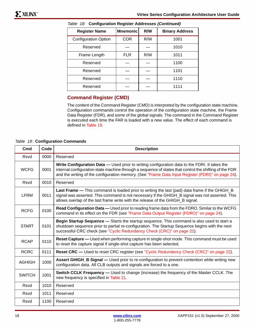
Virtex Series Configuration Architecture User GuideR13
Command Register (CMD)The content of the Command Register (CMD) is interpreted by the configuration state machineConfiguration commands control the operation of the configuration state machine the FrameData Register (FDR) and some of the global signals The command in the Command Registeris executed each time the FAR is loaded with a new value The effect of each command isdefined in Table 19
Configuration Option COR RW 1001
Reserved mdash mdash 1010
Frame Length FLR RW 1011
Reserved mdash mdash 1100
Reserved mdash mdash 1101
Reserved mdash mdash 1110
Reserved mdash mdash 1111
Table 18 Configuration Register Addresses (Continued)
Register Name Mnemonic RW Binary Address
Table 19 Configuration Commands
Cmd Code Description
Rsvd 0000 Reserved
WCFG 0001Write Configuration Data mdash Used prior to writing configuration data to the FDRI It takes theinternal configuration state machine through a sequence of states that control the shifting of the FDRand the writing of the configuration memory (See Frame Data Input Register (FDRI) on page 24)
Rsvd 0010 Reserved
LFRM 0011Last Frame mdash This command is loaded prior to writing the last (pad) data frame if the GHIGH_Bsignal was asserted This command is not necessary if the GHIGH_B signal was not asserted Thisallows overlap of the last frame write with the release of the GHIGH_B signal
RCFG 0100Read Configuration Data mdash Used prior to reading frame data from the FDRO Similar to the WCFGcommand in its effect on the FDR (see Frame Data Output Register (FDRO) on page 24)
START 0101Begin Startup Sequence mdash Starts the startup sequence This command is also used to start ashutdown sequence prior to partial re-configuration The Startup Sequence begins with the nextsuccessful CRC check (see Cyclic Redundancy Check (CRC) on page 22)
RCAP 0110Reset Capture mdash Used when performing capture in single-shot mode This command must be usedto reset the capture signal if single-shot capture has been selected
RCRC 0111 Reset CRC mdash Used to reset CRC register (see Cyclic Redundancy Check (CRC) on page 22)
AGHIGH 1000Assert GHIGH_B Signal mdash Used prior to re-configuration to prevent contention while writing newconfiguration data All CLB outputs and signals are forced to a one
SWITCH 1001Switch CCLK Frequency mdash Used to change (increase) the frequency of the Master CCLK Thenew frequency is specified in Table 21
Rsvd 1010 Reserved
Rsvd 1011 Reserved
Rsvd 1100 Reserved
18 wwwxilinxcom XAPP151 (v15) September 27 20001-800-255-7778
Virtex Series Configuration Architecture User GuideR13
Configuration Option Register (COR)The Configuration Option Register (COR) is used to select configuration options that areillustrated in Figure 15 and defined in Table 20 Entries in this table are further explained in thefollowing tables
Rsvd 1101 Reserved
Rsvd 1110 Reserved
Rsvd 1111 Reserved
Table 19 Configuration Commands (Continued)
Cmd Code Description
DO
NE
_PIP
E
DR
IVE
_DO
NE
SIN
GLE
OS
CF
SE
L
SS
CLK
SR
C
LOC
K_W
AIT
SH
UT
DO
WN
DO
NE
_CY
CLE
LCK
_CY
CLE
GT
S_C
YC
LE
GW
E_C
YC
LE
GS
R_C
YC
LE
31 30 29 28 27 26 25 24 23 22 21 20 19 18 17 16 15 14 13 12 11 10 9 8 7 6 5 4 3 2 1 00 x x x x x x x x x x x x x x x x x x x x x x x x x x x x x x x
Notes1 Locations within fields containing a zero or one must have these values An X in a bit field indicates that the value is variable and must
be set2 Heavy vertical lines are used to separate fields Light vertical lines separate nibbles in the word
Figure 15 COR (Configuration of Option Register) Fields
XAPP151 (v15) September 27 2000 wwwxilinxcom 191-800-255-7778
Virtex Series Configuration Architecture User GuideR13
Table 21 shows the allowed values for the OSCFSEL field of the COR Setting OSCFSEL toone of these values will set the Master CCLK frequency to the specified value
Table 20 Configuration Option Register Fields
Field Bit Indices DescriptionBitgenDefault
DONE_PIPE 30
0 No pipeline stage for DONEIN
1 Add pipeline stage to DONEINFPGA waits on DONE that is delayed by one (1) cycle of the StartupClkrather than the pin itself Use this option when StartupClk is running at highspeeds
0
DRIVE_DONE 290 DONE pin is open drain
1 DONE pin is actively driven high0
SINGLE 28 Readback capture is one-shot 0
OSCFSEL 2722 Select CCLK frequency in Master Serial configuration mode 2
SSCLKSRC 2120
Startup sequence clock source00 Cclk01 UserClk1x JTAGClk
0
LOCK_WAIT 1916
4-bit mask indicating which DLL lock signals to wait for during LCK cycleThe 4 bits (from MSB to LSB) correspond to DLLs TL=3 TR=2 BL=1BR=0 (top-left top-right etc) In Virtex-E devices where there are 8 DLLseach mask bit applies to the 2 DLLs in that quadrant of the device Thedefault is not to wait for any DLL lock signals
0
SHUTDOWN 15
Indicate whether doing a startup or shutdown sequence
0 Startup
1 Shutdown sequence
0
DONE_CYCLE 1412 Startup phase in which DONE pin is released 3
LCK_CYCLE 119 Stall in this startup phase until DLL locks are asserted 7
GTS_CYCLE 86 Startup phase in which IOs switch from tri-state to user design 4
GWE_CYCLE 53 Startup phase in which the global write-enable is asserted 5
GSR_CYCLE 20 Startup phase in which the global setreset is negated 5
Table 21 OSCFSEL-Specified Master CCLK Frequencies)
CCLK(MHz) OSCFSEL
CCLK(MHz) OSCFSEL
CCLK(MHz) OSCFSEL
43 000010 13 001010 41 100111
54 010001 15 001101 45 110011
69 000100 20 010111 51 101010
81 000101 26 011010 55 110100
20 wwwxilinxcom XAPP151 (v15) September 27 20001-800-255-7778
Virtex Series Configuration Architecture User GuideR13
Table 22 shows the values of the DONE_CYCLE LCK_CYCLE GTS_CYCLE GWE_CYCLEand GSR_CYCLE fields in COR This table shows the step in the start-up sequence when eachof these signals becomes active
Control Register (CTL)The Control Register (CTL) fields are illustrated in Figure 16 on page 21 and defined inTable 23
92 000110 30 011101 60 101101
100 000111 34 110010 mdash mdash
Notes1 These values are accurate to +45 ndash 30
Table 22 COR Startup Cycle Fields
FieldValue
DONE_CYCLE(DONE Active)
GTS_CYCLE(GTS_CFGInactive)
GSR_CYCLE(GSR Inactive)
GWE_CYCLE(GWE Active) LCK_CYCLE
000 1 1 1 1 0
001 2 2 2 2 1
010 3 3 3 3 2
011 4 (default) 4 4 4 3
100 5 5 (default) 5 5 4
101 6 6 6 (default) 6 (default) 5
110 mdash DoneIndagger DoneIndagger DoneIndagger 6
111 Keep State Keep State Keep State Keep State Donrsquot Wait(default)
Notes1 dagger DONE if DonePipe = No else the delayed version of DONE
Table 21 OSCFSEL-Specified Master CCLK Frequencies) (Continued)
CCLK(MHz) OSCFSEL
CCLK(MHz) OSCFSEL
CCLK(MHz) OSCFSEL
SB
ITS
PE
RS
IST
GT
S_U
SR
_B
31 30 29 28 27 26 25 24 23 22 21 20 19 18 17 16 15 14 13 12 11 10 9 8 7 6 5 4 3 2 1 00 0 0 0 0 0 0 0 0 0 0 0 0 0 0 0 0 0 0 0 0 0 0 x x x 0 0 0 0 0 x
Notes1 Locations within fields containing a zero or one must have these values An X in a bit field indicates that the value is variable and must
be set2 Heavy vertical lines are used to separate fields Light vertical lines separate nibbles in the word
Figure 16 Control Register Fields
XAPP151 (v15) September 27 2000 wwwxilinxcom 211-800-255-7778
Virtex Series Configuration Architecture User GuideR13
Cyclic Redundancy Check (CRC)A data input error checking mechanism is provided through the Cyclic Redundancy Check(CRC) register When data is written to any configuration register (except LOUT) a 16-bit CRCvalue is calculated using both the register data and the address This value is saved in the CRCregister At the end of any series of writes a pre-calculated CRC block-check value may bewritten to the CRC register If the resulting value is non-zero an error is indicated TheCRC_ERROR bit is accessible through the status register If a CRC error is detectedconfiguration logic is put in the ERROR mode The following section is an algorithm forcomputing CRC
CRC Algorithm Initialization bcc = 0skip_pad = truemore_words = true Check for write operation do
w = next_wordif (w[3127] == rsquo00101rsquo)
A Read OP Donrsquot use in CRCwc = w[100]if (wc == 0)
w = next_wordwc = w[190]
while (wc-- gt 0)
w = next_word
elsif (w[3127] == rsquo00110rsquo)
A Write OP Use in CRC addr = w[1613]if (addr Π0124569DB)
wc = w[100]if (wc == 0)
wc is in next word w = next_wordwc = w[190]
while (wc-- gt 0)
w = next_wordsw[350] = addr wordfor (i=0 ilt36 i++)
Table 23 Control Register Bits
NameBit
Indices Description
SBITS 87 Security level0 ReadWrite OK (default)1 Readback disabled23 Readback disabled Writing disabled except CRCregister
PERSIST 6 Configuration interface remains after configuration0 No (default)1 Yes
GTS_USR_B 0 Active-low global tristate IOs Turn off pull-ups ifGTS_CFG_B is also asserted
22 wwwxilinxcom XAPP151 (v15) September 27 20001-800-255-7778
Virtex Series Configuration Architecture User GuideR13
x16 = bcc[15] XOR sw[i]x15 = bcc[14] XOR x16x2 = bcc[1] XOR x16bcc[150] =
x15bcc[132]x2bcc[0]x16 Note the bit order crc[150] = bcc[015]
else
Pad word - ignore
while (more_words)
Frame Address Register (FAR)The Frame Address Register (FAR) holds the address of the current frame The address isdivided into three parts the block type the major address and the minor address The blocktype field indicates whether the CLB or block RAM address space is used The command in thecommand register is executed each time the FAR is loaded with a new value
The major address selects the CLB or RAM column the minor address selects the frame withinthe column The minor address is incremented each time a full data frame is read from orwritten to the frame data register If the last frame within the CLB column is selected when theincrement occurs the major address is incremented and the minor address is reset to zerootherwise the minor address is incremented However the block RAM major address is notincremented automatically
See Figure 18 for the definitions of valid values for the block type field The FAR field definitionsare shown in Figure 19
Figure 17 CRC Calculation Register
Note the Block RAM Major Address is not incremented automatically To address a differentBlock RAM Content column the FAR must be loaded with the new Major Address
Type CodesCLB 00RAM 01
Figure 18 Block Type Codes
x151_17_021100
15141312111098765432
1013
01234526272829303101
Address 32-bit Data Word
CRC Calculation Register
CRC Data Input Register
CRC Register [310]
DATA_IN
SHIFT
23
16-bit CRC13150
0000 0000 0000 0000133116
1313
XAPP151 (v15) September 27 2000 wwwxilinxcom 231-800-255-7778
Virtex Series Configuration Architecture User GuideR13
Frame Data Input Register (FDRI)The Frame Data Input Register (FDRI) is used to load configuration frame data into a Virtexdevice
The Frame Data Register (FDR) is a shift register into which data is loaded prior to transfer tothe configuration memory Configuration data is written to the Virtex device by loading thecommand register with the WCFG command and then loading the FDR with at least two framesof 32-bit words
The write operation is pipelined such that the first frame of data is written to the configurationmemory while the second frame is being shifted in The last frame (the pad frame) is alwaysdummy data which is not actually written to the configuration memory Each frame write mustinclude enough 32 bit data words to load the frame fully There is one pad word at the end ofeach frame which is required for the pipelining hardware
Frame Data Output Register (FDRO)The Frame Data Output Register (FDRO) is for reading configuration data or captured datafrom the Virtex device a process called readback Readback is performed by loading thecommand register with the RCFG command and then addressing the FDRO with a readcommand
Frame Length Register (FLR)Near the beginning of the configuration bitstream the Frame Length Register (FLR) is writtenwith the length of a frame as measured in 32-bit words This length count is used to providesequencing information for the configuration read and write operations Note that the FLR mustbe written before any FDR operation works It is not necessary to set the FLR more than onceIf the number of bits in a frame is not evenly divisible by 32 the length count of the frame mustbe rounded up to the next highest integer The values for the FLR for all the current Virtexseries devices are given in Table 24
BlockType
Major Address(Column Address)
Minor Address(Frame Address)
31 30 29 28 27 26 25 24 23 22 21 20 19 18 17 16 15 14 13 12 11 10 9 8 7 6 5 4 3 2 1 00 0 0 0 0 x x x x x x x x x x x x x x x x x x 0 0 0 0 0 0 0 0 0
Notes1 Locations within fields containing a zero or one must have these values An X in a bit field indicates that the value is variable and must
be set2 Heavy vertical lines are used to separate fields Light vertical lines separate nibbles in the word
Figure 19 Frame Address Fields (FAR)
Note The FLR contains a value that is one less than the number of words that are read fromor written to a given frame This is because the extra word needed for pipelining is not counted
Table 24 Frame Length Register Value
Device Row times Col Frame Length Words per Frame FLR Value
XCV50E 16 times 24 384 12 11
XCV100E 20 times 30 448 14 13
XCV150 24 times 36 512 16 15
XCV200E 28 times 42 576 18 17
XCV300E 32 times 48 672 21 20
24 wwwxilinxcom XAPP151 (v15) September 27 20001-800-255-7778
Virtex Series Configuration Architecture User GuideR13
Legacy Output Register (LOUT)The Legacy Output Register (LOUT) is used for daisy chaining the configuration bitstream toother Xilinx devices Data written to the LOUT is serialized and appears on the DOUT pin
Mask Register (MASK)The Mask Register (MASK) is a mask register for writes to the CTL register A 1 in bit N of themask allows that bit position to be written in the CTL register The default value of the mask isall 0s
Status Register (STAT)The Status Register (STAT) is loaded with current values of several control or status signalsThe register can be read via the re-configuration block or via JTAG The fields in the Statusregister are illustrated in Figure 20 The values of the signals given in Table 25 on page 26 canbe read from the status register
XCV400E 40 times 60 800 25 24
XCV405E 40 times 60 800 25 24
XCV600E 48 times 72 960 30 29
XCV800 56 times 84 1088 34 33
XCV812E 56 times 84 1088 34 33
XCV1000E 64 times 96 1248 39 38
XCV1600E 72 times 108 1376 43 42
XCV2000E 80 times 120 1536 48 47
XCV2600E 92 times 138 1728 54 53
XCV3200E 104 times 156 1952 61 60
Table 24 Frame Length Register Value (Continued)
Device Row times Col Frame Length Words per Frame FLR Value
DO
NE
INIT
MO
DE
GH
IGH
_B
GS
R_B
GW
E_B
GT
S_C
FG
IN_E
RR
OR
LOC
K
CR
C_E
RR
OR
31 30 29 28 27 26 25 24 23 22 21 20 19 18 17 16 15 14 13 12 11 10 9 8 7 6 5 4 3 2 1 00 0 0 0 0 0 0 0 0 0 0 0 0 0 0 0 0 x x x x x x x x x x x x x x x
Notes1 An X in a bit field indicates that the value is variable2 Heavy vertical lines are used to separate fields Light vertical lines separate nibbles in the word
Figure 20 Status Register Fields
XAPP151 (v15) September 27 2000 wwwxilinxcom 251-800-255-7778
Virtex Series Configuration Architecture User GuideR13
ConfigurationInterface
There are two configuration interfaces to the Virtex devices mdash the bit-serial Boundary Scaninterface and the 8-bit byte-serial SelectMAP interface Conceptually XCV50 configurationdata appears as in Figure 21
Frames and words within frames are written in the same order in both configuration interfacesstarting with Frame 0 word 0 (the left-most in the picture) followed by word 1 etc Bits withineach word are written from left to right (MSB first) in the bit-serial configuration interfaces
Within the SelectMAP interface data is written a byte at a time A sample word is shown inFigure 22 The top row indicates the device pin names The bottom row indicates the bit indiceswithin a configuration word Byte 0 loads first followed by byte 1 et cetera The MSB of eachbyte (ie bits 31 23 15 and 7) is loaded on pin D0 The LSB of each byte (ie bits 24 16 8and 0) is loaded on pin D7
PartialReconfigurationof CLBs
Partial reconfiguration can be performed with and without shutting down the device Ifcontention occurs it is advised to go through a shutdown sequence prior to loadingconfiguration frames When shutting down the DONE pin will go active and pull low If this is notdesireable the DONE pin can be prevented from going low by selecting the DONE_CYCLE toKeep State (111) Similarly to prevent GSR from becoming active and reseting the currentstate the GSR_CYCLE can be set to Keep State When not shutting down changes occurframe by frame but is completely done by the end of the Last Frame packet (see Example 1)
Table 25 Status Register Bits
Name Bit Indices Description
DONE 14 Input from DONE pin
INIT 13 Value of INIT
MODE 1210 Value of M2 M1 M0 mode pins
GHIGH_B 9 0 = GHIGH_B asserted
GSR_B 8 0 = all flip-flops are ResetSet
GWE_B 7 1 = flip-flops and block RAM are write disabled
GTS_CFG 6 0 = IOs are tri-stated
IN_ERROR 5 Legacy input error
LOCK 41 Output from DLL lock signals 1 = DLL is locked
CRC_ERROR 0 Indicates that a CRC error has occurred
Data Frame 0 (11 words) Pad Word
hellip
Data Frame n (11 words) Pad WordPad Frame (12 words)
Figure 21 XCV50 Frame Padding for Reads
Figure 22 SelectMAP Byte and Bit Ordering
x151_22_021100
D0 D1 D2 D3 D4 D5 D6 D7 D0 D1 D2 D3 D4 D5 D6 D7 D0 D1 D2 D3 D4 D5 D6 D7 D0 D1 D2 D3 D4 D5 D6 D7
Byte 0 Byte 1 Byte 2 Byte 313
26 wwwxilinxcom XAPP151 (v15) September 27 20001-800-255-7778
Virtex Series Configuration Architecture User GuideR13
The DONE pin will not change in this case Figure 23 illustrates a typical shutdownreconfiguration in the CLB address space and restart sequence
Examples Several examples of reading and evaluating configuration data are provided to illustrate thefollowing
Figure 23 Typical Shutdown Reconfiguration in the CLB Address Spaceand Restart Sequence
FFFF FFFF Dummy WordAA99 5566 Sync Word Does not realign an already synchronized SelectMap port3001 2001 COR0080 FF2F Shutdown bit set optionally set bit 29 DRIVE_DONE
Alternately COR may be read bit 15 set and written back3000 8001 CMD0000 0005 Start Shutdown3000 8001 CMD0000 0007 Reset CRC0000 00000000 0000 Clock shutdown sequence0000 00000000 00003000 8001 CMD0000 0008 Assert GHIGH3000 8001 CMD0000 0001 Write Configuration3000 2001 FAR0--- ---- Block Type CLB (00) MajorMinor Address3000 4--- FDRI + Word Count if count is lt1024 Otherwise use TypeII Header
Write FRAME DATAIf CLB Frames are not written to non-consecutive addresses repeat FAR word followedby new MajorMinor Address followed by FDRI + Word Count and then Frame Data
3000 0001 Write CRC---- ---- CRC3000 8001 CMD0000 0003 LFRM3000 4--- FDRI + Word Count
Write PAD FRAME
3001 2001 COR0080 3F2D Default COR Options
Alternately COR may be read bit 15 cleared and written back3000 8001 CMD0000 0005 Begin Startup3000 0001 Write CRC---- ---- CRC
0000 00000000 0000 4 Dummy Words0000 00000000 0000
Example 1 Read and Write Semaphores in an XCV100 at CLB R1 C1 Slice 0 on page 28Example 2 Reading the Complete Configuration from an XCV50 on page 33
XAPP151 (v15) September 27 2000 wwwxilinxcom 271-800-255-7778
Virtex Series Configuration Architecture User GuideR13
Example 1 Read and Write Semaphores in an XCV100 at CLB R1 C1Slice 0Semaphores are a useful communication mechanism documented in XAPP 153 ldquoStatus andControl Semaphore Registers using Partial Reconfigurationrdquo Figure 24 shows an abstractionof a microprocessor writing control information to an FPGA and reading status informationOne convention for implementing semaphores in Virtex devices is to use two bits of a 16-bitdual-port RAM as illustrated in Figure 25 This occupies one CLB slice with the F-LUTimplementing the control semaphore and the status semaphore implemented in the G-LUTAddress 15 of the G-LUT is used for on-chip writes to the semaphore and address 14 of the F-LUT is used for on-chip reads Conversely the off-chip microprocessor is reading the G-LUT[15] and writing F-LUT[14]
Example 3 Read the Slice 0 G-LUT from CLB R1 C1 from the Complete Configuration of anXCV50 on page 34Example 4 Read the Slice 1 F-LUT from CLB R19 C16 from an XCV100 on page 36Example 5 Read All Bits in Slice 0 G-LUTs from CLB C2 and XCV50 on page 39Example 6 Read Block SelectRAM index 387 of RAM R2 C0 from an XCV100E on page 41
Figure 24 Semaphore Abstraction
x151_ 23_021400
Status13
Control13
MicroProcessor FPGA13
Semaphores13
28 wwwxilinxcom XAPP151 (v15) September 27 20001-800-255-7778
Virtex Series Configuration Architecture User GuideR13
Using a Semaphore Abstraction dual-port RAM ensures that the LUT SelectRAMs are placedin the CLB in a predictable manner When writing data to one or more LUT SelectRAMs or flip-flops on the device all bits in the frame must have valid configuration information This isassured by altering valid configurations from bitstream files or from frames read from a properlyconfigured Virtex device The latter approach is used in this example
Figure 25 Semaphore ReadWrite Implementation
Frame 47
15
14
47 46
47 46
x151_ 24_021100
Select Map
Frame 46
DING
F
13
D2D3D4 5D6 7D0D1 D D
1
111
0
111
Chip Interface
G F
13
XAPP151 (v15) September 27 2000 wwwxilinxcom 291-800-255-7778
Virtex Series Configuration Architecture User GuideR13
Attributes for this design are summarized in Table 26
From the equations in Table 7 on page 11 the values shown in Table 27 can be calculated
From off-chip for reading the G-LUT[15] bit read one frame (MNA=47) For writing the F-LUT[14] bit we show how to read then write one frame (MNA=46) as opposed to modifyingdata from a bitstream file (both are valid methods) The frames on the XCV100 contain 13 32-bit words and one pad word Remember that fm_st_wd is calculated assuming the entireconfiguration has been read However only the pad frame and then frames 46 and 47 fromMajor Address 30 are being read The desired bit is in Frame 1 word 1 which is word 15
The commands for reading both frames (and the pad frame) are given in Figure 26
Table 26 Design Attributes for Example 1
Attribute
G-LUT [15] F-LUT [14]
Read Read Write
Chip_Rows 20
Chip_Cols 30
FL 14
CLB_Row 1
CLB_Col 1
Slice 0
FG 1 0
lut_bit 15 14
RW 1 1 0
Table 27 Semaphore Example Variables Equations and Values
Variable Equation
Value(s)
G-LUT[15] F-LUT[14]
Read Read Write
MJA 1 le 302 rArr 30 ndash 1 times 2 + 2 30
MNA lut_bit + 32ndash 0 times () 47 46
fm_bit_idx 3 + 18 times 1 ndash FG + RW times 32 52 53 21
fm_st_wd 14 times (8 + (30 ndash 1) times 48+ 4647) +RW times (14 +1)= 14 times (1400 + 4647) + 14 times RW= 19600 + 14 times 4647 + 14 times RW
20272 20258 20244
fm_wd floor (2032) 1 1 0
fm_wd_bit_idx 31 + 32 times 110 ndash 525321 11 10 10
30 wwwxilinxcom XAPP151 (v15) September 27 20001-800-255-7778
Virtex Series Configuration Architecture User GuideR13
The 42 words read are shown in Figure 27 F-LUT[14] is in the second frame (frame=1word=1) at bit 10 The value read is a 1 but because the LUT bits are inverted the logic valueis zero G-LUT[15] is in word one of the third data frame (frame=2 word=1) at bit 11The valueread is a 1 which is a logic zero
InstructionData
Hex 31 30 29 28 27 26 25 24 23 22 21 20 19 18 17 16 15 14 13 12 11 10 9 8 7 6 5 4 3 2 1 0
Sync Word AA99 5566 1 0 1 0 1 0 1 0 1 0 0 1 1 0 0 1 0 1 0 1 0 1 0 1 0 1 1 0 0 1 1 0
Write next (1) word to FAR 3000 2001 0 0 1 1 0 0 0 0 0 0 0 0 0 0 0 0 0 0 1 0 0 0 0 0 0 0 0 0 0 0 0 1
CLB MJA=30 MNA=46 003C 5800 0 0 0 0 0 0 0 0 0 0 1 1 1 1 0 0 0 1 0 1 1 1 0 0 0 0 0 0 0 0 0 0
Write next word to CMD 3000 8001 0 0 1 1 0 0 0 0 0 0 0 0 0 0 0 0 1 0 0 0 0 0 0 0 0 0 0 0 0 0 0 1
Register value for RCFG 0000 0004 0 0 0 0 0 0 0 0 0 0 0 0 0 0 0 0 0 0 0 0 0 0 0 0 0 0 0 0 0 1 0 0
Read from FDRO 2800 602A 0 0 1 0 1 0 0 0 0 0 0 0 0 0 0 0 0 1 1 0 0 0 0 0 0 0 1 0 1 0 1 0
Flush pipe 0000 0000 0 0 0 0 0 0 0 0 0 0 0 0 0 0 0 0 0 0 0 0 0 0 0 0 0 0 0 0 0 0 0 0
(read 42 words)
Notes1 Binary data is grouped in two ways for ease of interpretation Thin vertical lines separate nibble boundaries Heavy vertical lines
separate field boundaries
Figure 26 Commands to Read Two Data Frames
XAPP151 (v15) September 27 2000 wwwxilinxcom 311-800-255-7778
Virtex Series Configuration Architecture User GuideR13
To write to the F-LUT semaphore start with the second data frame (frame=1) that was justread Words 1 - 13 of that frame will become words 0 - 12 of the frame to be written Word 13of this new frame is a pad word and can have any value (typically 0 is chosen) In this newframe set bit 11 of word 0 (zero) to the desired value of the semaphore A pad frame mustfollow the data frame The commands from Figure 28 write these two frames into the device atthe proper location
Frame Word 31 30 29 28 27 26 25 24 23 22 21 20 19 18 17 16 15 14 13 12 11 10 9 8 7 6 5 4 3 2 1 0
0
0 1 1 1 1 1 1 1 1 1 1 1 1 1 1 1 1 1 1 1 1 1 1 1 1 1 1 1 1 1 1 1 1
1 1 1 1 1 1 1 1 1 1 1 1 1 1 1 1 1 1 1 1 1 1 1 1 1 1 1 1 1 1 1 1 1
2 1 1 1 1 1 1 1 1 1 1 1 1 1 1 1 1 1 1 1 1 1 1 1 1 1 1 1 1 1 1 1 1
3 1 1 1 1 1 1 1 1 1 1 1 1 1 1 1 1 1 1 1 1 1 1 1 1 1 1 1 1 1 1 1 1
4 1 1 1 1 1 1 1 1 1 1 1 1 1 1 1 1 1 1 1 1 1 1 1 1 1 1 1 1 1 1 1 1
5 1 1 1 1 1 1 1 1 1 1 1 1 1 1 1 1 1 1 1 1 1 1 1 1 1 1 1 1 1 1 1 1
6 1 1 1 1 1 1 1 1 1 1 1 1 1 1 1 1 1 1 1 1 1 1 1 1 1 1 1 1 1 1 1 1
7 1 1 1 1 1 1 1 1 1 1 1 1 1 1 1 1 1 1 1 1 1 1 1 1 1 1 1 1 1 1 1 1
8 1 1 1 1 1 1 1 1 1 1 1 1 1 1 1 1 1 1 1 1 1 1 1 1 1 1 1 1 1 1 1 1
9 1 1 1 1 1 1 1 1 1 1 1 1 1 1 1 1 1 1 1 1 1 1 1 1 1 1 1 1 1 1 1 1
10 1 1 1 1 1 1 1 1 1 1 1 1 1 1 1 1 1 1 1 1 1 1 1 1 1 1 1 1 1 1 1 1
11 1 1 1 1 1 1 1 1 1 1 1 1 1 1 1 1 1 1 1 1 1 1 1 1 1 1 1 1 1 1 1 1
12 1 1 1 1 1 1 1 1 1 1 1 1 1 1 1 1 1 1 1 1 1 1 1 1 1 1 1 1 1 1 1 1
13 1 1 1 1 1 1 1 1 1 1 1 1 1 1 1 1 1 1 1 1 1 1 1 1 1 1 1 1 1 1 1 1
1
0 0 0 0 0 0 0 0 0 0 0 0 0 0 0 0 0 0 0 0 0 0 0 0 0 0 0 0 0 0 0 0 0
1 1 0 0 0 0 0 0 0 0 0 0 0 1 0 0 0 0 1 1 0 1 1 0 0 0 0 0 0 0 0 0 0 F[14]
2 1 1 1 1 1 0 1 1 0 0 0 0 1 1 1 1 0 0 1 1 1 1 1 0 1 1 0 0 0 0 0 0
3 0 0 0 0 1 1 1 1 1 0 1 1 0 0 0 0 0 0 0 0 0 0 1 1 1 1 1 0 1 1 0 0
4 0 0 0 0 0 0 0 0 1 1 1 1 0 0 0 0 0 0 0 0 0 0 0 0 0 0 1 1 1 1 1 0
5 1 1 0 0 1 1 0 0 0 0 0 0 1 1 0 0 1 0 1 1 0 0 0 0 0 0 0 0 0 0 1 1
6 1 1 1 0 1 1 0 0 0 0 0 0 1 1 1 0 1 1 1 0 1 0 1 1 0 0 0 0 0 0 0 0
7 0 0 1 1 1 1 1 0 1 1 0 0 0 0 1 1 0 0 0 0 1 1 1 1 1 0 1 1 0 0 0 0
8 0 0 0 0 0 0 1 1 1 1 1 0 0 0 0 0 0 0 0 0 0 0 0 0 1 1 1 1 1 0 1 1
9 0 0 0 0 0 0 0 0 0 0 1 1 0 0 0 0 1 1 0 0 0 0 0 0 0 0 0 0 1 1 1 1
10 1 0 1 1 0 0 0 0 0 0 0 0 1 0 1 1 1 1 1 0 1 1 0 0 0 0 0 0 0 0 0 0
11 1 1 1 1 1 0 1 1 0 0 0 0 1 1 1 1 0 0 1 1 1 1 1 0 1 1 0 0 0 0 0 0
12 0 0 0 0 1 1 0 1 1 0 1 1 0 0 0 0 0 0 0 0 0 0 1 1 1 1 1 0 0 0 0 0
13 0 0 0 0 0 0 1 1 0 1 0 1 0 0 0 0 0 0 0 0 0 0 0 0 0 0 0 0 0 0 0 0
2
0 0 0 0 0 0 0 0 0 0 0 0 0 0 0 0 0 0 0 0 0 0 0 0 0 0 0 0 0 0 0 0 0
1 1 0 1 0 0 0 0 0 0 0 0 1 1 0 1 0 1 1 1 0 1 1 0 0 0 0 0 0 0 0 0 0 G[15]
2 1 1 1 1 1 1 1 1 0 0 0 0 1 1 1 1 0 0 1 1 1 1 1 1 1 1 0 0 0 0 0 0
3 0 0 0 0 1 1 1 1 1 1 1 1 0 0 0 0 0 0 0 0 0 0 1 0 1 1 1 1 1 1 0 0
4 0 0 0 0 0 0 0 0 1 1 1 1 0 0 0 0 0 0 0 0 0 0 0 0 0 0 1 1 1 1 1 1
5 1 1 0 0 0 0 0 0 0 0 0 0 1 1 0 0 1 1 1 1 0 0 1 0 0 0 0 0 0 0 1 1
6 1 1 1 1 1 1 0 0 0 0 0 0 1 1 1 1 1 1 1 1 1 1 1 1 0 0 0 0 0 0 0 0
7 0 0 1 1 1 1 1 1 1 1 0 0 0 0 1 1 0 0 0 0 1 1 1 1 1 1 1 1 0 0 0 0
8 0 0 0 0 0 0 1 1 1 1 1 1 0 0 0 0 0 0 0 0 0 0 0 0 1 1 1 1 1 1 1 1
9 0 0 0 0 0 0 0 0 0 0 1 1 0 0 0 0 1 1 0 0 0 0 0 0 0 0 0 0 1 1 1 1
10 1 1 1 1 0 0 0 0 0 0 0 0 1 1 1 1 1 1 1 1 1 1 0 0 0 0 0 0 0 0 0 0
11 1 1 1 1 1 1 1 1 0 0 0 0 1 1 1 1 0 0 1 1 1 1 1 1 1 1 0 0 0 0 0 0
12 0 0 0 0 1 1 0 1 1 1 1 1 0 0 0 0 0 0 0 0 0 0 1 1 1 1 1 0 1 0 0 0
13 0 0 0 0 0 1 1 0 0 1 1 1 0 0 0 0 0 0 0 0 0 0 0 0 0 0 0 0 0 0 0 0
Figure 27 Three Frames Containing the Semaphores
32 wwwxilinxcom XAPP151 (v15) September 27 20001-800-255-7778
Virtex Series Configuration Architecture User GuideR13
Example 2 Reading the Complete Configuration from an XCV50Steps
1 If flip-flop values are needed clock the on-chip signal CAPTURE to capture flip-flopvalues See the Xilinx Libraries Guide for use of the CAPTURE_VIRTEX cell
2 Write the starting frame address (CLB MJA=0 MNA=0) into the FAR
3 Write the RCFG command to the CMD register
4 Address the FDRO register with a READ operation and word count equal to the number of32-bit words in the CLB frames plus one pad frame
5 Read the data following the timing diagrams in the SelectMAP interface section
6 Write the address for RAM block 0 to the FAR
7 Address the FDRO register with a read operation and word count equal to the number of32-bit words in the RAM block plus one pad frame
8 Read the data
9 Write the address for RAM block 1 to the FAR
10 Address the FDRO register with a read operation and word count equal to the number of32-bit words in the RAM block plus one pad frame
11 Read the data
When using SelectMAP mode to read data words from the Virtex device de-assert CS de-assert WRITE assert CS then clock the data out When using JTAG load the JTAG IR
InstructionData
Hex 31 30 29 28 27 26 25 24 23 22 21 20 19 18 17 16 15 14 13 12 11 10 9 8 7 6 5 4 3 2 1 0
Sync Word AA995566
1 0 1 0 1 0 1 0 1 0 0 1 1 0 0 1 0 1 0 1 0 1 0 1 0 1 1 0 0 1 1 0
Write next (1) word to FAR 30002001
0 0 1 1 0 0 0 0 0 0 0 0 0 0 0 0 0 0 1 0 0 0 0 0 0 0 0 0 0 0 0 1
MJA=30 MNA=46 003C5C00
0 0 0 0 0 0 0 0 0 0 1 1 1 1 0 0 0 1 0 1 1 1 0 0 0 0 0 0 0 0 0 0
Write next word to CMD 30008001
0 0 1 1 0 0 0 0 0 0 0 0 0 0 0 0 1 0 0 0 0 0 0 0 0 0 0 0 0 0 0 1
Register value for WCFG 00000001
0 0 0 0 0 0 0 0 0 0 0 0 0 0 0 0 0 0 0 0 0 0 0 0 0 0 0 0 0 0 0 1
Write 28 words to FDRI 3000401C
0 0 1 1 0 0 0 0 0 0 0 0 0 0 0 0 0 1 0 0 0 0 0 0 0 0 0 1 1 1 0 0
Data Word 0 A01AEC00
1 0 1 0 0 0 0 0 0 0 0 1 1 0 1 0 1 1 1 0 1 1 0 0 0 0 0 0 0 0 0 0
Data Word 1 FF0F3FC0
1 1 1 1 1 1 1 1 0 0 0 0 1 1 1 1 0 0 1 1 1 1 1 1 1 1 0 0 0 0 0 0
Data Word 2 0FF002FC
0 0 0 0 1 1 1 1 1 1 1 1 0 0 0 0 0 0 0 0 0 0 1 0 1 1 1 1 1 1 0 0
hellip hellip hellip
Data Word 27 00000000
0 0 0 0 0 0 0 0 0 0 0 0 0 0 0 0 0 0 0 0 0 0 0 0 0 0 0 0 0 0 0 0
Notes1 Binary data is grouped in two ways for ease of interpretation Thin vertical lines separate nibble boundaries Heavy
vertical lines separate field boundaries
Figure 28 Commands to Write a Semaphore Value
XAPP151 (v15) September 27 2000 wwwxilinxcom 331-800-255-7778
Virtex Series Configuration Architecture User GuideR13
(instruction register) with the CFG_OUT instruction Then go to the SDR (Shift-DR) state andshift the data out (See Figure 29)
Example 3 Read the Slice 0 G-LUT from CLB R1 C1 from the CompleteConfiguration of an XCV50The commands for reading the bitstream from the Virtex device are given in Example 1 Readand Write Semaphores in an XCV100 at CLB R1 C1 Slice 0 on page 28 Using an XCV50device the independent attributes are show in Table 28
InstructionData
Hex 31 30 29 28 27 26 25 24 23 22 21 20 19 18 17 16 15 14 13 12 11 10 9 8 7 6 5 4 3 2 1 0
Sync Word AA99 5566 1 0 1 0 1 0 1 0 1 0 0 1 1 0 0 1 0 1 0 1 0 1 0 1 0 1 1 0 0 1 1 0
Write next word to FAR 3000 2001 0 0 1 1 0 0 0 0 0 0 0 0 0 0 0 0 0 0 1 0 0 0 0 0 0 0 0 0 0 0 0 1
CLB MJA=0 MNA=0 0000 0000 0 0 0 0 0 0 0 0 0 0 0 0 0 0 0 0 0 0 0 0 0 0 0 0 0 0 0 0 0 0 0 0
Write next word to CMDregister
3000 8001 0 0 1 1 0 0 0 0 0 0 0 0 0 0 0 0 1 0 0 0 0 0 0 0 0 0 0 0 0 0 0 1
Register value for RCFG 0000 0004 0 0 0 0 0 0 0 0 0 0 0 0 0 0 0 0 0 0 0 0 0 0 0 0 0 0 0 0 0 1 0 0
Read from FDRO register 2800 6000 0 0 1 0 1 0 0 0 0 0 0 0 0 0 0 0 0 1 1 0 0 0 0 0 0 0 0 0 0 0 0 0
15876 words 4800 3E04 0 1 0 0 1 0 0 0 0 0 0 0 0 0 0 0 0 0 1 1 1 1 1 0 0 0 0 0 0 1 0 0
Flush pipe 0000 0000 0 0 0 0 0 0 0 0 0 0 0 0 0 0 0 0 0 0 0 0 0 0 0 0 0 0 0 0 0 0 0 0
(Read 15876 words)Write to FAR register 3000 2001 0 0 1 1 0 0 0 0 0 0 0 0 0 0 0 0 0 0 1 0 0 0 0 0 0 0 0 0 0 0 0 1
RAM MJA=0 MNA=0 0200 0000 0 0 0 0 0 0 1 0 0 0 0 0 0 0 0 0 0 0 0 0 0 0 0 0 0 0 0 0 0 0 0 0
Read 780 words fromFDRO reg
2800 630C 0 0 1 0 1 0 0 0 0 0 0 0 0 0 0 0 0 1 1 0 0 0 1 1 0 0 0 0 1 1 0 0
Flush pipe 0000 0000 0 0 0 0 0 0 0 0 0 0 0 0 0 0 0 0 0 0 0 0 0 0 0 0 0 0 0 0 0 0 0 0
(Read 780 words)Write to FAR register 3000 2001 0 0 1 1 0 0 0 0 0 0 0 0 0 0 0 0 0 0 1 0 0 0 0 0 0 0 0 0 0 0 0 1
RAM MJA=1 MNA=0 0202 0000 0 0 0 0 0 0 1 0 0 0 0 0 0 0 1 0 0 0 0 0 0 0 0 0 0 0 0 0 0 0 0 0
Read 780 words fromFDRO reg
2800 630C 0 0 1 0 1 0 0 0 0 0 0 0 0 0 0 0 0 1 1 0 0 0 1 1 0 0 0 0 1 1 0 0
Flush pipe 0000 0000 0 0 0 0 0 0 0 0 0 0 0 0 0 0 0 0 0 0 0 0 0 0 0 0 0 0 0 0 0 0 0 0
(Read 780 words)
Figure 29 Example 2 - Read Complete Configuration for XCV50
Table 28 XCV50 Independent Attributes
Independent Attributes Values
Chip_Rows 16
Chip_Cols 24
FL 12
CLB_Row 1
CLB_Col 1
FG 1
Slice 0
RW 1
34 wwwxilinxcom XAPP151 (v15) September 27 20001-800-255-7778
Virtex Series Configuration Architecture User GuideR13
From the equations given earlier in Table 7 calculating the range of values for fm_st_wdindicates that the word 13740 of the configuration is the starting word of the 12-word (FL=12)frame containing bit 0 of the G-LUT in Slice 0 of CLB R1C1 (Table 29)
The configuration bits for the given frame are as follows G-LUT[0] is in fm_wd=0 at bit 11
All 16 LUT SelectRAM bits are in the following words at the same bit index 11
Table 29 Variables Equations and Values for Slice 0 G-LUT
Variables Equations Values
MJA 1 le 242 rArr 24 ndash 1times 2 + 2 24
MNA 0 times (hellip) + lut_bit + 32 0 321 332 343 35
4 365 376 387 39
8 409 41
10 4211 43
12 4413 4514 4615 47
fm_bit_idx 3 + 18 times 1 ndash1 + RW times 32 52
fm_st_wd 12 times (8+ (24 ndash1) times 48 + [3247]) +1 x 12= 12 times (1112 + [3247]) +12= 13356 + 12 times 3247]
1374013920
fm_wd floor(5232) 1
fm_wd_bit_idx 31 + 32 ndash 52 11
BitstreamWord
Frame 32-bit Word FrameWord31 30 29 28 27 26 25 24 23 22 21 20 19 18 17 16 15 14 13 12 11 10 9 8 7 6 5 4 3 2 1 0
13740 0 0 0 0 0 0 0 0 0 0 0 0 0 0 0 0 0 0 0 0 0 0 0 0 0 0 0 0 0 0 0 0 013741 0 0 1 0 1 0 0 0 0 0 0 0 0 1 0 1 0 1 0 0 1 1 1 0 0 0 0 0 0 0 0 0 113742 1 0 1 1 0 0 1 1 0 0 0 0 0 0 0 0 0 0 1 0 1 1 0 0 1 1 0 0 0 0 0 0 213743 0 0 0 0 1 0 1 1 0 0 1 1 0 0 0 0 0 0 0 0 0 0 1 0 1 1 0 0 1 1 0 0 313744 0 0 0 0 0 0 0 0 1 0 1 1 0 0 1 1 0 0 0 0 0 0 0 0 0 0 1 0 1 1 0 0 413745 1 1 0 0 0 0 0 0 0 0 0 0 1 0 1 1 0 0 1 1 0 0 0 0 0 0 0 0 0 0 1 0 513746 1 1 0 0 1 1 0 0 0 0 0 0 0 0 0 0 1 0 1 1 0 0 1 1 0 0 0 0 0 0 0 0 613747 0 0 1 0 1 1 0 0 1 1 0 0 0 0 0 0 0 0 0 0 1 0 1 1 0 0 1 1 0 0 0 0 713748 0 0 0 0 0 0 1 0 1 1 0 0 1 1 0 0 0 0 0 0 0 0 0 0 1 0 1 1 0 0 1 1 813749 0 0 0 0 0 0 0 0 0 0 1 0 1 1 0 0 1 1 0 0 0 0 0 0 0 0 0 0 1 0 1 1 913750 0 0 1 1 0 0 0 0 0 0 0 0 0 0 1 0 1 1 0 0 1 0 1 0 0 0 0 0 0 0 0 0 1013751 0 1 0 1 0 0 0 0 0 0 0 0 0 0 0 0 0 0 0 0 0 0 0 0 0 0 0 0 0 0 0 0 11
Figure 30 Configuration Bits for Slice 0 CLB R1C1 G-LUT [0]
XAPP151 (v15) September 27 2000 wwwxilinxcom 351-800-255-7778
Virtex Series Configuration Architecture User GuideR13
The 16 bits are LUT[150]=0111111111111111 The LUT SelectRAM bits are inverted from theirlogic values The ldquologicalrdquo contents are LUT[150]=1000000000000000 Thus this G-LUTimplements a 4-input AND function
Example 4 Read the Slice 1 F-LUT from CLB R19 C16 from an XCV100Commands for reading the bitstream from the Virtex device are given in Figure 32 Use thefollowing independent attributes to find the given F-LUT
From the equations in Table 7 on page 11 calculating fm_st_wd indicates the starting wordwith respect to a configuration that starts at MJA=0 MNA=0 Because the frames we are
BitstreamWord
Frame 32-bit Word
LUT Bit31 30 29 28 27 26 25 24 23 22 21 20 19 18 17 16 15 14 13 12 11 10 9 8 7 6 5 4 3 2 1 0
13741 0 0 1 0 1 0 0 0 0 0 0 0 0 1 0 1 0 1 0 0 1 1 1 0 0 0 0 0 0 0 0 0 0
13753 1 0 1 0 0 0 0 0 0 0 0 0 0 0 0 1 0 0 0 1 1 1 0 0 0 0 0 0 0 0 0 0 1
13765 1 0 1 0 1 0 0 0 0 0 0 0 1 0 0 0 0 0 0 1 1 1 1 0 0 0 0 0 0 0 0 0 2
13777 0 0 0 0 1 0 0 0 0 0 0 1 1 1 0 1 1 0 1 0 1 1 0 0 0 0 0 0 0 0 0 0 3
13789 0 1 0 0 0 0 0 0 0 0 0 0 0 1 0 1 1 1 1 1 1 1 1 0 0 0 0 0 0 0 0 0 4
13801 1 0 1 0 1 0 0 0 0 0 0 1 0 0 0 1 1 0 0 1 1 1 0 0 0 0 0 0 0 0 0 0 5
13813 0 0 0 1 0 0 0 0 0 0 0 0 0 0 0 0 1 0 0 1 1 1 0 0 0 0 0 0 0 0 0 0 6
13825 0 1 1 0 1 0 0 0 0 0 0 1 0 1 0 0 1 1 0 0 1 1 0 0 0 0 0 0 0 0 0 0 7
13837 1 0 1 1 1 0 0 0 0 0 0 1 0 1 0 1 1 0 0 0 1 1 0 0 0 0 0 0 0 0 0 0 8
13849 1 0 0 0 0 0 0 0 0 0 0 0 0 0 0 0 1 1 1 0 1 1 0 0 0 0 0 0 0 0 0 0 9
13861 1 0 0 0 0 0 0 0 0 0 0 1 0 0 0 0 1 1 1 1 1 1 1 0 0 0 0 0 0 0 0 0 10
13873 1 0 0 0 0 0 0 1 0 0 0 0 0 1 0 0 0 1 1 0 1 1 0 0 0 1 0 0 0 0 0 0 11
13885 1 0 0 0 0 0 0 0 0 0 0 0 0 1 0 1 0 0 1 0 1 1 0 0 0 0 0 0 0 0 0 0 12
13897 0 0 0 0 1 0 0 0 0 0 0 0 0 1 0 0 0 0 0 0 1 1 0 0 0 0 0 0 0 0 0 0 13
13909 1 0 0 0 0 0 0 0 0 0 0 0 1 1 0 1 0 1 1 0 1 1 0 0 0 0 0 0 0 0 0 0 14
13921 1 0 1 0 0 0 0 0 0 0 0 1 1 1 0 1 1 1 1 1 0 1 0 0 0 0 0 0 0 0 0 0 15
Figure 31 Location of all 16 LUT SelectRAM Bits
Table 30 Virtex Bitstream Command Attributes
Independent Attributes Values
Chip_Rows 20
Chip_Cols 30
FL 14
CLB_Row 19
CLB_Col 16
FG 0
Slice 1
RW 1
36 wwwxilinxcom XAPP151 (v15) September 27 20001-800-255-7778
Virtex Series Configuration Architecture User GuideR13
interested in start at MJA=1 MNA=0 which is fm_st_wd = 126 so the first 126 words are notneeded (0ndash125) Therefore to find the given Slice 1 F-LUT see Table 31
Sixteen frames need to be read one for each bit in the LUT SelectRAM The bits in LUTSelectRAMs in Slice 1 occur in the opposite order that they do for Slice 0 LUT SelectRAMs
Frames are read sequentially with ascending addresses If read in LUT bit order LUT[0]LUT[1] hellip LUT[15] These are stored in descending addresses which require 16 separateread operations each reading one data frame and one pad frame However if read inascending address order LUT[15] LUT[14] hellip LUT[0] all 16 data frames are read with asingle read operation This requires only one pad frame for all 16 frames Thus it takes lesstime to read ascending frames starting at MJA=1 MNA=0 and finishing with frame MJA=1MNA=15 The frames in the XCV100 contain 14 32-bit words and a single pad wordCommands for reading only the F-LUT data are given in Figure 32
Table 31 Variables Equations and Values for Slice 1 F-LUT
Variables Equations Values
MJA 16 gt 302 rArr 2times16 ndash 30 ndash1 1
MNA lut_bit + 32 ndash Slice times (2 times lut_bit +17)= [015] + 32 ndash (2 times [015] + 17)= 15 ndash [015]
0 151 142 133 12
4 115 106 97 8
8 79 6
10 511 4
12 313 214 115 0
fm_bit_idx 3 + 18 times 19 ndash 0+ 32 377
fm_st_wd 14 times (8 + (1ndash 1) times 48 + [150]) +1 times 14= 14 times (8 + [150]) +14= 126 + 14 times [150]
= 336126
fm_wd floor(37732) 11
fm_wd_bit_idx 31 + 32 times 11 ndash 377 6
XAPP151 (v15) September 27 2000 wwwxilinxcom 371-800-255-7778
Virtex Series Configuration Architecture User GuideR13
The 377th bit of each frame is the bit in the F-LUT This LUT SelectRAM bit is in the framersquosword index 11 bit index 6
The configuration bits for the given frame in Figure 33 are as follows LUT Bit 15 is in MJA=1MNA=0 fm_wd=11 at bit 6
LUT bit 0 is in MJA=1 MNA=15 fm_wd=11 at bit 6
InstructionData
Hex 31 30 29 28 27 26 25 24 23 22 21 20 19 18 17 16 15 14 13 12 11 10 9 8 7 6 5 4 3 2 1 0
Sync Word AA99 5566 1 0 1 0 1 0 1 0 1 0 0 1 1 0 0 1 0 1 0 1 0 1 0 1 0 1 1 0 0 1 1 0
Write next (1) word to FAR 3000 2001 0 0 1 1 0 0 0 0 0 0 0 0 0 0 0 0 0 0 1 0 0 0 0 0 0 0 0 0 0 0 0 1
CLB MJA = 1 MNA = 0 0002 0000 0 0 0 0 0 0 0 0 0 0 0 0 0 0 1 0 0 0 0 0 0 0 0 0 0 0 0 0 0 0 0 0
Write next word to CMD 3000 8001 0 0 1 1 0 0 0 0 0 0 0 0 0 0 0 0 1 0 0 0 0 0 0 0 0 0 0 0 0 0 0 1
Register value for RCFG 0000 0004 0 0 0 0 0 0 0 0 0 0 0 0 0 0 0 0 0 0 0 0 0 0 0 0 0 0 0 0 0 1 0 0
Read from FDRO 2800 60EE 0 0 1 0 1 0 0 0 0 0 0 0 0 0 0 0 0 1 1 0 0 0 0 0 1 1 1 0 1 1 1 0
Flush pipe 0000 0000 0 0 0 0 0 0 0 0 0 0 0 0 0 0 0 0 0 0 0 0 0 0 0 0 0 0 0 0 0 0 0 0
(Read 238 words)
Figure 32 Commands to read Slice 1 F-LUT
Frame WordFrame 32-bit Word
31 30 29 28 27 26 25 24 23 22 21 20 19 18 17 16 15 14 13 12 11 10 9 8 7 6 5 4 3 2 1 0
0 0 0 0 0 0 0 0 0 0 0 0 0 0 0 0 0 0 0 0 0 0 0 0 0 0 0 0 0 0 0 0 0
1 1 1 0 0 0 0 0 0 0 0 0 0 0 1 0 1 1 1 1 1 1 1 0 0 0 0 0 0 0 0 0 0
2 1 1 1 1 1 1 1 1 0 0 0 0 0 0 0 0 0 0 1 1 1 1 1 1 1 1 0 0 0 0 0 0
3 0 0 0 0 1 1 1 1 1 1 1 1 0 0 0 0 0 0 0 0 0 0 1 1 1 1 1 1 1 1 0 0
4 0 0 0 0 0 0 0 0 1 1 1 1 1 1 1 1 0 0 0 0 0 0 0 0 0 0 1 1 1 1 1 1
5 1 1 0 0 0 0 0 0 0 0 0 0 1 1 1 1 1 1 1 1 0 0 0 0 0 0 0 0 0 0 1 1
6 1 1 1 1 1 1 0 0 0 0 0 0 0 0 0 0 1 1 1 1 1 1 1 1 0 0 0 0 0 0 0 0
7 0 0 1 1 1 1 1 1 1 1 0 0 0 0 0 0 0 0 0 0 1 1 1 1 1 1 1 1 0 0 0 0
8 0 0 0 0 0 0 1 1 1 1 1 1 1 1 0 0 0 0 0 0 0 0 0 0 1 1 1 1 1 1 1 1
9 0 0 0 0 0 0 0 0 0 0 1 1 1 1 1 1 1 1 0 0 0 0 0 0 0 0 0 0 1 1 1 1
10 1 1 1 1 0 0 0 0 0 0 0 0 0 0 1 1 1 1 1 1 1 1 0 0 0 0 0 0 0 0 0 0
11 1 1 1 1 1 1 1 1 0 0 0 0 0 0 0 0 0 0 1 1 1 1 1 1 1 0 0 0 0 0 0 0
12 0 0 0 0 1 1 1 1 1 1 1 1 0 0 0 0 0 0 0 0 0 0 1 1 1 1 1 1 0 0 0 0
13 0 0 0 0 0 0 0 0 0 1 1 1 0 0 0 0 0 0 0 0 0 0 1 1 1 1 1 1 0 0 0 0
Figure 33 Frame Containing F-LUT[15]
Bit streamWord
Frame 32-bit WordFmWd31 30 29 28 27 26 25 24 23 22 21 20 19 18 17 16 15 14 13 12 11 10 9 8 7 6 5 4 3 2 1 0
336 0 0 0 0 0 0 0 0 0 0 0 0 0 0 0 0 0 0 0 0 0 0 0 0 0 0 0 0 0 0 0 0 0337 0 1 0 0 1 0 0 0 0 0 0 1 0 1 0 0 1 1 0 0 1 1 0 0 0 0 0 0 0 0 0 0 1338 1 0 1 1 0 0 1 1 0 0 0 0 0 0 0 0 0 0 1 0 1 1 0 0 1 1 0 0 0 0 0 0 2339 0 0 0 0 1 0 1 1 0 0 1 1 0 0 0 0 0 0 0 0 0 0 1 0 1 1 0 0 1 1 0 0 3340 0 0 0 0 0 0 0 0 1 0 1 1 0 0 1 1 0 0 0 0 0 0 0 0 0 0 1 0 1 1 0 0 4341 1 1 0 0 0 0 0 0 0 0 0 0 1 0 1 1 0 0 1 1 0 0 0 0 0 0 0 0 0 0 1 0 5342 1 1 0 0 1 1 0 0 0 0 0 0 0 0 0 0 1 0 1 1 0 0 1 1 0 0 0 0 0 0 0 0 6343 0 0 1 0 1 1 0 0 1 1 0 0 0 0 0 0 0 0 0 0 1 0 1 1 0 0 1 1 0 0 0 0 7
Figure 34 Frame Containing F-LUT [0]
38 wwwxilinxcom XAPP151 (v15) September 27 20001-800-255-7778
Virtex Series Configuration Architecture User GuideR13
For the sake of brevity here are the sixteen 11th words in the order they appear in thebitstream
The bits are LUT[150]=0111111111111111 The LUT SelectRAM bits are inverted from thelogic sense The logical contents are LUT[150]=1000000000000000 Thus this F-LUTimplements a 4-input AND gate
Example 5 Read All Bits in Slice 0 G-LUTs from CLB C2 and XCV50Given the following attributes the necessary values to find the G-LUT data can be computed
344 0 0 0 0 0 0 1 0 1 1 0 0 1 1 0 0 0 0 0 0 0 0 0 0 1 0 1 1 0 0 1 1 8345 0 0 0 0 0 0 0 0 0 0 1 0 1 1 0 0 1 1 0 0 0 0 0 0 0 0 0 0 1 0 1 1 9346 0 0 1 1 0 0 0 0 0 0 0 0 0 0 1 0 1 1 0 0 1 1 0 0 0 0 0 0 0 0 0 0 10347 1 1 1 1 1 0 1 1 0 0 0 0 0 0 0 0 0 0 1 0 1 1 1 0 1 1 0 1 0 0 0 0 11348 0 0 0 0 1 1 1 0 1 0 1 1 0 0 0 0 0 0 0 0 0 0 1 1 1 1 0 1 0 0 0 0 12349 0 0 0 0 0 1 0 0 0 0 1 0 0 0 0 0 0 0 0 0 0 0 0 0 0 0 0 0 0 0 0 0 13
Bit streamWord
Frame 32-bit WordFmWd31 30 29 28 27 26 25 24 23 22 21 20 19 18 17 16 15 14 13 12 11 10 9 8 7 6 5 4 3 2 1 0
Figure 34 Frame Containing F-LUT [0]
BitstreamWord
Frame 32-bit WordLUT Bit31 30 29 28 27 26 25 24 23 22 21 20 19 18 17 16 15 14 13 12 11 10 9 8 7 6 5 4 3 2 1 0
137 1 1 1 1 1 1 1 1 0 0 0 0 0 0 0 0 0 0 1 1 1 1 1 1 1 0 0 0 0 0 0 0 15151 1 0 1 1 1 0 1 1 0 0 0 0 0 0 0 0 0 0 1 0 1 1 1 0 1 1 0 0 0 0 0 0 14165 1 0 1 1 0 0 1 1 0 0 0 0 0 0 0 0 0 0 1 0 1 1 1 0 1 1 0 0 0 0 0 0 13179 1 0 1 1 1 0 1 1 0 0 0 0 0 0 0 0 0 0 1 0 1 1 1 0 1 1 0 0 0 0 0 0 12193 1 1 1 1 1 0 1 1 0 0 0 0 0 0 0 0 0 0 1 1 1 1 1 0 1 1 0 0 0 0 0 0 11207 1 1 1 1 1 1 1 1 0 0 0 0 0 0 0 0 0 0 1 1 1 1 1 1 1 1 1 0 1 0 0 0 10221 1 1 1 1 1 0 1 1 0 0 0 0 0 0 0 0 0 0 1 1 1 1 1 0 1 1 0 0 0 0 0 0 9235 1 0 1 1 1 0 1 1 0 0 0 0 0 0 0 0 0 0 1 0 1 1 1 0 1 1 0 0 0 0 0 0 8249 1 0 1 1 0 0 1 1 0 0 0 0 0 0 0 0 0 0 1 0 1 1 0 0 1 1 0 0 0 0 0 0 7263 1 0 1 1 0 1 1 1 1 0 0 0 0 0 0 0 0 0 1 0 1 1 0 1 1 1 0 0 0 0 0 0 6277 1 1 1 1 0 0 1 1 0 0 0 0 0 0 0 0 0 0 1 1 1 1 0 0 1 1 0 0 0 0 0 0 5291 1 1 1 1 1 1 1 1 0 0 0 0 0 0 0 0 0 0 1 1 1 1 1 1 1 1 0 0 0 0 0 0 4305 1 1 1 1 1 0 1 1 0 0 0 0 0 0 0 0 0 0 1 1 1 1 1 0 1 1 0 0 0 0 0 0 3319 1 0 1 1 0 1 1 1 0 0 0 0 0 0 0 0 0 0 1 0 1 1 0 1 1 1 0 0 0 0 0 0 2333 1 0 1 1 0 0 1 1 0 0 0 0 0 0 0 0 0 0 1 0 1 1 0 0 1 1 0 0 0 0 0 0 1347 1 1 1 1 1 0 1 1 0 0 0 0 0 0 0 0 0 0 1 0 1 1 1 0 1 1 0 1 0 0 0 0 0
Figure 35 Sixteen Words Containing the F-LUT bit
Table 32 All Bits Slice 0 GndashLUTs from CLB C2 and XCV50
Independent Attributes Values
Chip_Rows 16
Chip_Cols 24
FL 12
CLB_Row 116
CLB_Col 2
XAPP151 (v15) September 27 2000 wwwxilinxcom 391-800-255-7778
Virtex Series Configuration Architecture User GuideR13
From the equations in Table 7 the dependent variables can be calculated
Note that fm_bit_idx fm_wd and fm_wd_bit_idx have 16 values one for each row on theXCV50 Figure 37 shows where the data lies in the first frame which contains G[0] for the entirecolumn The process is the same for the other 15 frames The commands for reading the LUTSelectRAM data are given in Figure 36
From the calculation for fm_st_wd Frame 0 would start at word 12588 reading the wholeconfiguration The instructions in Figure 36 start at that word so word 0 (ignoring the 12 wordsin the pad frame) is the same as word 12588 of the entire CLB configuration The 12 words inthe frame are shown in Figure 37
FG 1
Slice 0
lut_bit 015
RW 1
Table 32 All Bits Slice 0 GndashLUTs from CLB C2 and XCV50 (Continued)
Independent Attributes Values
Table 33 Dependent Variables Equations and Values
Variables Equations Values
MJA 2 le 242 rArr 24 ndash 2times 2 + 2 22
MNAlut_bit + 32 ndash Slice times (2 times lut_bit + 17)= lut_bit + 32 ndash 0 times (2 times lut_bit + 17)= [015] + 32
032 436 840 1244
133 537 941 1345
234 638 1042 1456
335 739 1143 1547
fm_bit_idx3 + 18 times CLB_Row ndash 1+ 32 = 34 + 18 times[116]
152 5124 9196 13268
270 6142 10214 14286
388 7160 11232 15304
4106 8178 12250 16322
fm_st_wd12 times (8 + (22 ndash1) times 48 + MNA) + 1 times 12= 12 times (1016 + MNA) + 12= 12204 + 12 times MNA
0 12588 4 12636 8 12684 12 12732
1 12600 5 12648 9 12696 13 12744
2 12612 6 12660 10 12708 14 12756
3 12624 7 12672 11 12720 15 12768
fm_wd floor (fm_bit_idx32)
11 53 96 138
22 64 106 148
32 75 117 159
43 85 127 1610
fm_wd_bit_idx 31 + 32 times fm_wd ndash fm_bit_idx
111 53 927 1319
225 617 109 141
37 7 31 1123 1515
421 813 125 1629
40 wwwxilinxcom XAPP151 (v15) September 27 20001-800-255-7778
Virtex Series Configuration Architecture User GuideR13
The LUT SelectRAM bits have been shaded for ease of identification It can be seen from thecalculation of fm_bit_idx that the LUT SelectRAM bits are in the order 116 For example fromthe above calculations for fm_wd and fm_wd_bit_idx G-LUT[0] in R1C2 is in fm_wd 1fm_wd_bit_idx 11 This bit is the shaded bit in word 1 at bit index 11 Similarly the G-LUT[0] forthe other 15 CLB rows are also shaded in this table
Example 6 Read Block SelectRAM index 387 of RAM R2 C0 from anXCV100ECommands for reading the bitstream from the Virtex device are given in Figure 38 Use thefollowing independent attributes to find the given F-LUT
InstructionData
Hex 31 30 29 28 27 26 25 24 23 22 21 20 19 18 17 16 15 14 13 12 11 10 9 8 7 6 5 4 3 2 1 0
Sync Word AA99 5566 1 0 1 0 1 0 1 0 1 0 0 1 1 0 0 1 0 1 0 1 0 1 0 1 0 1 1 0 0 1 1 0
Write next (1) word to FAR 3000 2001 0 0 1 1 0 0 0 0 0 0 0 0 0 0 0 0 0 0 1 0 0 0 0 0 0 0 0 0 0 0 0 1
CLB MJA=22 MNA=32 002C 4000 0 0 0 0 0 0 0 0 0 0 1 0 1 1 0 0 0 1 0 0 0 0 0 0 0 0 0 0 0 0 0 0
Write next word to CMD 3000 8001 0 0 1 1 0 0 0 0 0 0 0 0 0 0 0 0 1 0 0 0 0 0 0 0 0 0 0 0 0 0 0 1
Register value for RCFG 0000 0004 0 0 0 0 0 0 0 0 0 0 0 0 0 0 0 0 0 0 0 0 0 0 0 0 0 0 0 0 0 1 0 0
Read from FDRO 2800 60CC 0 0 1 0 1 0 0 0 0 0 0 0 0 0 0 0 0 1 1 0 0 0 0 0 1 1 0 0 1 1 0 0
Flush pipe 0000 0000 0 0 0 0 0 0 0 0 0 0 0 0 0 0 0 0 0 0 0 0 0 0 0 0 0 0 0 0 0 0 0 0
(Read 204 words)
Figure 36 Commands to read RC2S0 G-LUT
WordFrame 32-bit Word
CLB Row31 30 29 28 27 26 25 24 23 22 21 20 19 18 17 16 15 14 13 12 11 10 9 8 7 6 5 4 3 2 1 0
0 0 0 0 0 0 0 0 0 0 0 0 0 0 0 0 0 0 0 0 0 0 0 0 0 0 0 0 0 0 0 0 0
1 0 0 0 0 1 0 0 0 0 0 0 0 0 1 0 1 0 1 0 0 1 1 0 0 0 0 0 0 0 0 0 0 12 1 0 1 1 0 0 1 1 0 0 0 0 0 0 0 0 0 0 1 0 1 1 0 0 1 1 0 0 0 0 0 0 2 33 0 0 0 0 1 0 1 1 0 0 1 1 0 0 0 0 0 0 0 0 0 0 1 0 1 1 0 0 1 1 0 0 4 54 0 0 0 0 0 0 0 0 1 0 1 1 0 0 1 1 0 0 0 0 0 0 0 0 0 0 1 0 1 1 0 0 65 1 1 0 0 0 0 0 0 0 0 0 0 1 0 1 1 0 0 1 1 0 0 0 0 0 0 0 0 0 0 1 0 7 86 1 1 0 0 1 1 0 0 0 0 0 0 0 0 0 0 1 0 1 1 0 0 1 1 0 0 0 0 0 0 0 0 9 107 0 0 1 0 1 1 0 0 1 1 0 0 0 0 0 0 0 0 0 0 1 0 1 1 0 0 1 1 0 0 0 0 11 128 0 0 0 0 0 0 1 0 1 1 0 0 1 1 0 0 0 0 0 0 0 0 0 0 1 0 1 1 0 0 1 1 13 149 0 0 0 0 0 0 0 0 0 0 1 0 1 1 0 0 1 1 0 0 0 0 0 0 0 0 0 0 1 0 1 1 15
10 0 0 1 1 0 0 0 0 0 0 0 0 0 0 1 0 1 1 0 0 1 0 1 0 0 0 0 0 0 0 0 0 1611 0 1 0 1 0 0 0 0 0 0 0 0 0 0 0 0 0 0 0 0 0 0 0 0 0 0 0 0 0 0 0 0
Figure 37 Frame for RC2S0 G-LUTs Bit G[0]
Table 34 Virtex Bitstream Command Attributes
Independent Attributes Values
Chip_Rams 4
FL 14
RAM_Row 2
RAM_Col 0
ram_bit 387
RW 1
XAPP151 (v15) September 27 2000 wwwxilinxcom 411-800-255-7778
Virtex Series Configuration Architecture User GuideR13
Since we are attempting to read only one bit location only one frame is necessary to be readWe use the equations of Table 15 Table 16 and Table 17 to determine the dependentvariables
Commands for reading this memory index are given in Figure 38
RAM bit 387 is at fm_wd=6 bit 4
Table 35 Variables Equations and Values for Slice 1 F-LUT
Variables Equations Values
MJA_virtex 0 lt42 rArr 2times(42 -1 -0) 2
MJA_adj 0 lt42 rArr 2 2
MJA MJA_virtex + MJA_adj 4
MNA floor(((38764)64)32)+ 2 x floor(((38764)32)16)+ 4 x floor(((38764)16)8) + 8 x floor(((38764)8)4)+ 16 x floor(((38764)4)2) + 32 x floor(((38764)2)1)
24
fm_bit_idx 3 + 18 times 19 ndash 0 + 32 219
fm_st_wd 14 x 24 + 1 x 14 350
fm_wd floor(21932) 6
fm_wd_bit_idx 31 + 32 times 6 ndash 219 4
InstructionData
Hex 31 30 29 28 27 26 25 24 23 22 21 20 19 18 17 16 15 14 13 12 11 10 9 8 7 6 5 4 3 2 1 0
Sync Word AA99 5566 1 0 1 0 1 0 1 0 1 0 0 1 1 0 0 1 0 1 0 1 0 1 0 1 0 1 1 0 0 1 1 0
Write next (1) word to FAR 3000 2001 0 0 1 1 0 0 0 0 0 0 0 0 0 0 0 0 0 0 1 0 0 0 0 0 0 0 0 0 0 0 0 1
CLB MJA = 4 MNA = 24 0208 3000 0 0 0 0 0 0 1 0 0 0 0 0 1 0 0 0 0 0 1 1 0 0 0 0 0 0 0 0 0 0 0 0
Write next word to CMD 3000 8001 0 0 1 1 0 0 0 0 0 0 0 0 0 0 0 0 1 0 0 0 0 0 0 0 0 0 0 0 0 0 0 1
Register value for RCFG 0000 0004 0 0 0 0 0 0 0 0 0 0 0 0 0 0 0 0 0 0 0 0 0 0 0 0 0 0 0 0 0 1 0 0
Read from FDRO 2800 601C 0 0 1 0 1 0 0 0 0 0 0 0 0 0 0 0 0 1 1 0 0 0 0 0 0 0 0 1 1 1 0 0
Flush pipe 0000 0000 0 0 0 0 0 0 0 0 0 0 0 0 0 0 0 0 0 0 0 0 0 0 0 0 0 0 0 0 0 0 0 0
(Read 28 words)
Figure 38 Commands to read Block SelectRAM index 387
42 wwwxilinxcom XAPP151 (v15) September 27 20001-800-255-7778
Virtex Series Configuration Architecture User GuideR13
Glossary Block SelectRAM Resource
One of several large fully-synchronous dual-port memories in the Virtex FPGAs Each ofthese memories contain 4096 bits The organization of each memory is configurable Theblock SelectRAM resource complements the smaller distributed LUT SelectRAMs
Boundary Scan Interface
One of the configuration interfaces on the Virtex device This is a bit-serial interface TheBoundary Scan interface is also known as the JTAG port Also see the SelectMAP interface
Capture Data
The flip-flop and pad data saved from the logic cells and IO blocks into the bitstream Use theCAPTURE_VIRTEX primitive in your HDL code to specify the trigger and clock for the captureoperation
Configurable Logic Block (CLB)
The functional elements for constructing logic circuits The Virtex CLB is made up of Sliceswhich contain Logic Cells
Configuration Bitstream
Configuration commands optionally with configuration data
Configuration Commands
Instructions for the Virtex device There are two classes of Configuration Command mdash Majorand Minor The Major Commands read and write data to configuration registers in the Virtexdevice The Minor commands instruct the Virtex configuration logic to perform specificfunctions See Command Register (CMD) on page 18
Configuration Data
Bits that directly define the state of programmable logic These are written to a Virtex device ina configuration bitstream and read as Readback Data from a Virtex device
Frame WordFrame 32-bit Word
31 30 29 28 27 26 25 24 23 22 21 20 19 18 17 16 15 14 13 12 11 10 9 8 7 6 5 4 3 2 1 0
0 0 0 0 0 0 0 0 0 0 0 0 0 0 0 0 0 0 0 0 0 0 0 0 0 0 0 0 0 0 0 0 0
1 1 1 0 0 0 0 0 0 0 0 0 0 0 1 0 1 1 1 1 1 1 1 0 0 0 0 0 0 0 0 0 0
2 1 1 1 1 1 1 1 1 0 0 0 0 0 0 0 0 0 0 1 1 1 1 1 1 1 1 0 0 0 0 0 0
3 0 0 0 0 1 1 1 1 1 1 1 1 0 0 0 0 0 0 0 0 0 0 1 1 1 1 1 1 1 1 0 0
4 0 0 0 0 0 0 0 0 1 1 1 1 1 1 1 1 0 0 0 0 0 0 0 0 0 0 1 1 1 1 1 1
5 1 1 0 0 0 0 0 0 0 0 0 0 1 1 1 1 1 1 1 1 0 0 0 0 0 0 0 0 0 0 1 1
6 1 1 1 1 1 1 0 0 0 0 0 0 0 0 0 0 1 1 1 1 1 1 1 1 0 0 0 0 0 0 0 0
7 0 0 1 1 1 1 1 1 1 1 0 0 0 0 0 0 0 0 0 0 1 1 1 1 1 1 1 1 0 0 0 0
8 0 0 0 0 0 0 1 1 1 1 1 1 1 1 0 0 0 0 0 0 0 0 0 0 1 1 1 1 1 1 1 1
9 0 0 0 0 0 0 0 0 0 0 1 1 1 1 1 1 1 1 0 0 0 0 0 0 0 0 0 0 1 1 1 1
10 1 1 1 1 0 0 0 0 0 0 0 0 0 0 1 1 1 1 1 1 1 1 0 0 0 0 0 0 0 0 0 0
11 1 1 1 1 1 1 1 1 0 0 0 0 0 0 0 0 0 0 1 1 1 1 1 1 1 0 0 0 0 0 0 0
12 0 0 0 0 1 1 1 1 1 1 1 1 0 0 0 0 0 0 0 0 0 0 1 1 1 1 1 1 0 0 0 0
13 0 0 0 0 0 0 0 0 0 1 1 1 0 0 0 0 0 0 0 0 0 0 1 1 1 1 1 1 0 0 0 0
Figure 39 Frame MNA=24
XAPP151 (v15) September 27 2000 wwwxilinxcom 431-800-255-7778
Virtex Series Configuration Architecture User GuideR13
Configuration Frame
The configuration bits in a Virtex device are organized in columns A column of CLBs with theIO blocks above and below the CLBs contain 48 frames of configuration bits The smallestnumber of bits that can be read or written through the configuration interfaces is one frame
Configuration Interface
A logical interface on the Virtex device through which configuration commands and data can beread and written A interface consists of one or more physical Device Pins
Configuration Readback
The operation of reading Configuration Data (also known as Readback Data) from a Virtexdevice
Device Pin
One of the electrical connections on the package containing the Virtex device
Frame
See Configuration Frame
Logic Cell (LC)
The basic building block of the Virtex CLB An LC includes a 4-input function generator carrylogic and a storage element
LUT SelectRAMs
Shallow RAM structures implemented in CLB Lookup Tables (LUTs) See also blockSelectRAM section
Pad
Pad bits are extra bits used to make the total number of bits in a frame an integral multiple of32 the number of bits in a configuration word A Pad Word is an extra word used at the end ofa Configuration Frame for pipelining A Pad Frame is an extra Configuration Frame used at thebeginning of a Configuration Readback and at the end of a Configuration Write for pipelining
Readback Data
Configuration data read from a Virtex device The data is organized as Configuration Frames
SelectMAP Interface
One of the configuration interfaces on the Virtex device This is a byte-serial interface The pinsin the SelectMAP interface may be used as user IO after configuration has been completed orremain configured as a configuration interface
Slice
A subdivision of the Virtex CLB There are two vertical slices in a Virtex CLB Each slicecontains two Logic Cells
Sync Word
A 32-bit word with a value that is used to synchronize the configuration logic
44 wwwxilinxcom XAPP151 (v15) September 27 20001-800-255-7778
Virtex Series Configuration Architecture User GuideR13
RevisionHistory
The following table shows the revision history for this document
Date Version Revision
061799 10 Initial Release
072799 11 Updated the following tables Table 5 equation for MNA Table 7equations for MJA amp fm_bit_idx
092099 12 Changes in page 5 Most formulae in Table 7 have been revisedDocumented pad capture value P Corrected bit locations inExamples
022200 13 Updated to include Virtex-E block SelectRAM Correctedfm_bit_idx (Right IOB) equations in Table 12 and fm_st_wddefinition Corrected CRC algorithm Various corrections inExamples Reformatted and edited document and figures
080300 14 Updated to include Virtex-EM devices in Table 3 and Table 24
092700 15 Added Partial Reconfiguration of CLB section and Figure 26
XAPP151 (v15) September 27 2000 wwwxilinxcom 451-800-255-7778
- Summary
- Introduction
-
- CLBs IOBs and Configurations
-
- Configuring Virtex Devices
- Reading Configuration Bits From a Virtex Device
-
- Configuration Columns
- Configuration Addressing
-
- Block Type Major Address Minor Address
-
- Virtex Major Addresses
- Virtex-EM Major Addresses
- Virtex-E Major Addresses
-
- Frames
-
- Frame Sizes
- Frame Organization
- Location of LUT SelectRAM Bits
-
- Configuration Data Operations
-
- Reading Configuration Data
- Writing Configuration Data
- Altering Configuration Data
-
- Definitions
- CLB LUT SelectRAM Dependent Variables
-
- Virtex-E CLB LUT SelectRAM Dependent Variables
- LUT SelectRAM Examples
-
- CLB Flip-Flop Dependent Variables
-
- Virtex-E CLB Flip-Flop Dependent Variables
-
- IOB Dependent Variables
-
- Virtex-E IOB Dependent Variables
-
- Block SelectRAM Dependent Variables
-
- Virtex-E Block SelectRAM Dependent Variables
-
- Configuration Logic Basics
-
- Configuration Data
- Configuration Flow
-
- For Initial Configuration
- Reading Configuration
- Writing Configuration
-
- Configuration Registers
-
- Command Register (CMD)
- Configuration Option Register (COR)
- Control Register (CTL)
- Cyclic Redundancy Check (CRC)
-
- CRC Algorithm
-
- Frame Address Register (FAR)
- Frame Data Input Register (FDRI)
- Frame Data Output Register (FDRO)
- Frame Length Register (FLR)
- Legacy Output Register (LOUT)
- Mask Register (MASK)
- Status Register (STAT)
-
- Configuration Interface
- Partial Reconfiguration of CLBs
- Examples
-
- Example 1 Read and Write Semaphores in an XCV100 at CLB R1 C1 Slice 0
- Example 2 Reading the Complete Configuration from an XCV50
- Example 3 Read the Slice 0 G-LUT from CLB R1 C1 from the Complete Configuration of an XCV50
- Example 4 Read the Slice 1 F-LUT from CLB R19 C16 from an XCV100
- Example 5 Read All Bits in Slice 0 G-LUTs from CLB C2 and XCV50
- Example 6 Read Block SelectRAM index 387 of RAM R2 C0 from an XCV100E
-
- Glossary
-
- Block SelectRAM Resource
- Boundary Scan Interface
- Capture Data
- Configurable Logic Block (CLB)
- Configuration Bitstream
- Configuration Commands
- Configuration Data
- Configuration Frame
- Configuration Interface
- Configuration Readback
- Device Pin
- Frame
- Logic Cell (LC)
- LUT SelectRAMs
- Pad
- Readback Data
- SelectMAP Interface
- Slice
- Sync Word
-
- Revision History
-
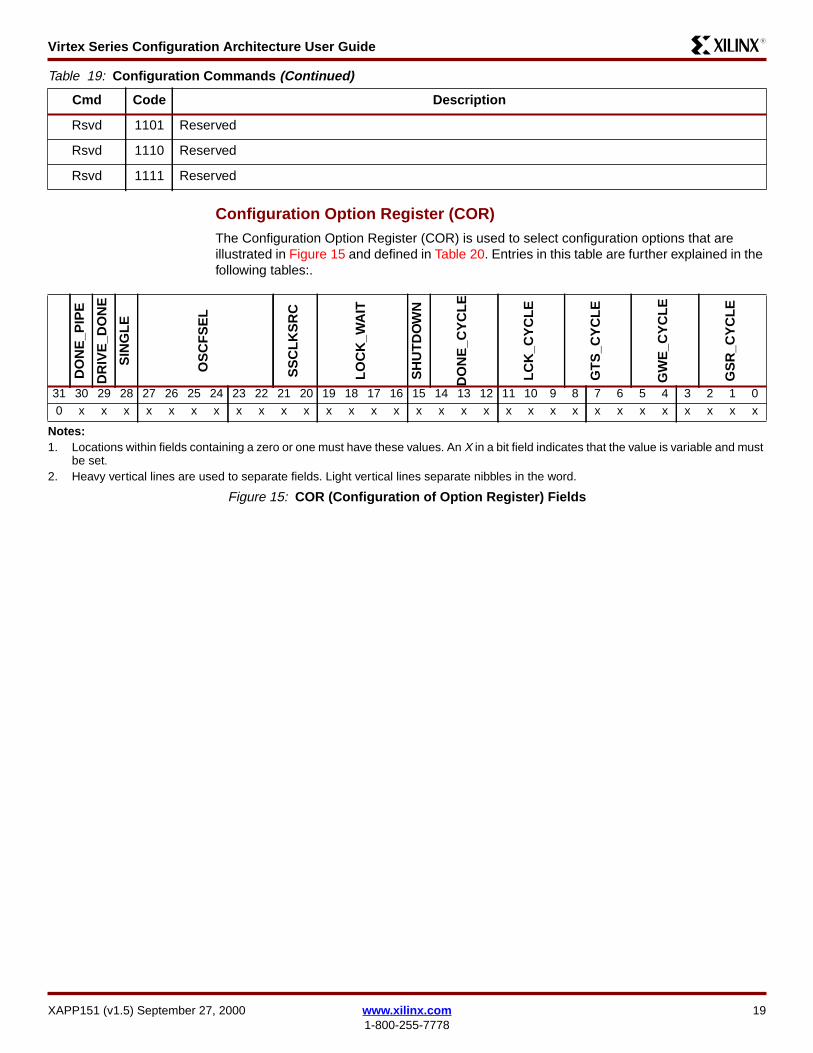
Virtex Series Configuration Architecture User GuideR13
Configuration Option Register (COR)The Configuration Option Register (COR) is used to select configuration options that areillustrated in Figure 15 and defined in Table 20 Entries in this table are further explained in thefollowing tables
Rsvd 1101 Reserved
Rsvd 1110 Reserved
Rsvd 1111 Reserved
Table 19 Configuration Commands (Continued)
Cmd Code Description
DO
NE
_PIP
E
DR
IVE
_DO
NE
SIN
GLE
OS
CF
SE
L
SS
CLK
SR
C
LOC
K_W
AIT
SH
UT
DO
WN
DO
NE
_CY
CLE
LCK
_CY
CLE
GT
S_C
YC
LE
GW
E_C
YC
LE
GS
R_C
YC
LE
31 30 29 28 27 26 25 24 23 22 21 20 19 18 17 16 15 14 13 12 11 10 9 8 7 6 5 4 3 2 1 00 x x x x x x x x x x x x x x x x x x x x x x x x x x x x x x x
Notes1 Locations within fields containing a zero or one must have these values An X in a bit field indicates that the value is variable and must
be set2 Heavy vertical lines are used to separate fields Light vertical lines separate nibbles in the word
Figure 15 COR (Configuration of Option Register) Fields
XAPP151 (v15) September 27 2000 wwwxilinxcom 191-800-255-7778
Virtex Series Configuration Architecture User GuideR13
Table 21 shows the allowed values for the OSCFSEL field of the COR Setting OSCFSEL toone of these values will set the Master CCLK frequency to the specified value
Table 20 Configuration Option Register Fields
Field Bit Indices DescriptionBitgenDefault
DONE_PIPE 30
0 No pipeline stage for DONEIN
1 Add pipeline stage to DONEINFPGA waits on DONE that is delayed by one (1) cycle of the StartupClkrather than the pin itself Use this option when StartupClk is running at highspeeds
0
DRIVE_DONE 290 DONE pin is open drain
1 DONE pin is actively driven high0
SINGLE 28 Readback capture is one-shot 0
OSCFSEL 2722 Select CCLK frequency in Master Serial configuration mode 2
SSCLKSRC 2120
Startup sequence clock source00 Cclk01 UserClk1x JTAGClk
0
LOCK_WAIT 1916
4-bit mask indicating which DLL lock signals to wait for during LCK cycleThe 4 bits (from MSB to LSB) correspond to DLLs TL=3 TR=2 BL=1BR=0 (top-left top-right etc) In Virtex-E devices where there are 8 DLLseach mask bit applies to the 2 DLLs in that quadrant of the device Thedefault is not to wait for any DLL lock signals
0
SHUTDOWN 15
Indicate whether doing a startup or shutdown sequence
0 Startup
1 Shutdown sequence
0
DONE_CYCLE 1412 Startup phase in which DONE pin is released 3
LCK_CYCLE 119 Stall in this startup phase until DLL locks are asserted 7
GTS_CYCLE 86 Startup phase in which IOs switch from tri-state to user design 4
GWE_CYCLE 53 Startup phase in which the global write-enable is asserted 5
GSR_CYCLE 20 Startup phase in which the global setreset is negated 5
Table 21 OSCFSEL-Specified Master CCLK Frequencies)
CCLK(MHz) OSCFSEL
CCLK(MHz) OSCFSEL
CCLK(MHz) OSCFSEL
43 000010 13 001010 41 100111
54 010001 15 001101 45 110011
69 000100 20 010111 51 101010
81 000101 26 011010 55 110100
20 wwwxilinxcom XAPP151 (v15) September 27 20001-800-255-7778
Virtex Series Configuration Architecture User GuideR13
Table 22 shows the values of the DONE_CYCLE LCK_CYCLE GTS_CYCLE GWE_CYCLEand GSR_CYCLE fields in COR This table shows the step in the start-up sequence when eachof these signals becomes active
Control Register (CTL)The Control Register (CTL) fields are illustrated in Figure 16 on page 21 and defined inTable 23
92 000110 30 011101 60 101101
100 000111 34 110010 mdash mdash
Notes1 These values are accurate to +45 ndash 30
Table 22 COR Startup Cycle Fields
FieldValue
DONE_CYCLE(DONE Active)
GTS_CYCLE(GTS_CFGInactive)
GSR_CYCLE(GSR Inactive)
GWE_CYCLE(GWE Active) LCK_CYCLE
000 1 1 1 1 0
001 2 2 2 2 1
010 3 3 3 3 2
011 4 (default) 4 4 4 3
100 5 5 (default) 5 5 4
101 6 6 6 (default) 6 (default) 5
110 mdash DoneIndagger DoneIndagger DoneIndagger 6
111 Keep State Keep State Keep State Keep State Donrsquot Wait(default)
Notes1 dagger DONE if DonePipe = No else the delayed version of DONE
Table 21 OSCFSEL-Specified Master CCLK Frequencies) (Continued)
CCLK(MHz) OSCFSEL
CCLK(MHz) OSCFSEL
CCLK(MHz) OSCFSEL
SB
ITS
PE
RS
IST
GT
S_U
SR
_B
31 30 29 28 27 26 25 24 23 22 21 20 19 18 17 16 15 14 13 12 11 10 9 8 7 6 5 4 3 2 1 00 0 0 0 0 0 0 0 0 0 0 0 0 0 0 0 0 0 0 0 0 0 0 x x x 0 0 0 0 0 x
Notes1 Locations within fields containing a zero or one must have these values An X in a bit field indicates that the value is variable and must
be set2 Heavy vertical lines are used to separate fields Light vertical lines separate nibbles in the word
Figure 16 Control Register Fields
XAPP151 (v15) September 27 2000 wwwxilinxcom 211-800-255-7778
Virtex Series Configuration Architecture User GuideR13
Cyclic Redundancy Check (CRC)A data input error checking mechanism is provided through the Cyclic Redundancy Check(CRC) register When data is written to any configuration register (except LOUT) a 16-bit CRCvalue is calculated using both the register data and the address This value is saved in the CRCregister At the end of any series of writes a pre-calculated CRC block-check value may bewritten to the CRC register If the resulting value is non-zero an error is indicated TheCRC_ERROR bit is accessible through the status register If a CRC error is detectedconfiguration logic is put in the ERROR mode The following section is an algorithm forcomputing CRC
CRC Algorithm Initialization bcc = 0skip_pad = truemore_words = true Check for write operation do
w = next_wordif (w[3127] == rsquo00101rsquo)
A Read OP Donrsquot use in CRCwc = w[100]if (wc == 0)
w = next_wordwc = w[190]
while (wc-- gt 0)
w = next_word
elsif (w[3127] == rsquo00110rsquo)
A Write OP Use in CRC addr = w[1613]if (addr Π0124569DB)
wc = w[100]if (wc == 0)
wc is in next word w = next_wordwc = w[190]
while (wc-- gt 0)
w = next_wordsw[350] = addr wordfor (i=0 ilt36 i++)
Table 23 Control Register Bits
NameBit
Indices Description
SBITS 87 Security level0 ReadWrite OK (default)1 Readback disabled23 Readback disabled Writing disabled except CRCregister
PERSIST 6 Configuration interface remains after configuration0 No (default)1 Yes
GTS_USR_B 0 Active-low global tristate IOs Turn off pull-ups ifGTS_CFG_B is also asserted
22 wwwxilinxcom XAPP151 (v15) September 27 20001-800-255-7778
Virtex Series Configuration Architecture User GuideR13
x16 = bcc[15] XOR sw[i]x15 = bcc[14] XOR x16x2 = bcc[1] XOR x16bcc[150] =
x15bcc[132]x2bcc[0]x16 Note the bit order crc[150] = bcc[015]
else
Pad word - ignore
while (more_words)
Frame Address Register (FAR)The Frame Address Register (FAR) holds the address of the current frame The address isdivided into three parts the block type the major address and the minor address The blocktype field indicates whether the CLB or block RAM address space is used The command in thecommand register is executed each time the FAR is loaded with a new value
The major address selects the CLB or RAM column the minor address selects the frame withinthe column The minor address is incremented each time a full data frame is read from orwritten to the frame data register If the last frame within the CLB column is selected when theincrement occurs the major address is incremented and the minor address is reset to zerootherwise the minor address is incremented However the block RAM major address is notincremented automatically
See Figure 18 for the definitions of valid values for the block type field The FAR field definitionsare shown in Figure 19
Figure 17 CRC Calculation Register
Note the Block RAM Major Address is not incremented automatically To address a differentBlock RAM Content column the FAR must be loaded with the new Major Address
Type CodesCLB 00RAM 01
Figure 18 Block Type Codes
x151_17_021100
15141312111098765432
1013
01234526272829303101
Address 32-bit Data Word
CRC Calculation Register
CRC Data Input Register
CRC Register [310]
DATA_IN
SHIFT
23
16-bit CRC13150
0000 0000 0000 0000133116
1313
XAPP151 (v15) September 27 2000 wwwxilinxcom 231-800-255-7778
Virtex Series Configuration Architecture User GuideR13
Frame Data Input Register (FDRI)The Frame Data Input Register (FDRI) is used to load configuration frame data into a Virtexdevice
The Frame Data Register (FDR) is a shift register into which data is loaded prior to transfer tothe configuration memory Configuration data is written to the Virtex device by loading thecommand register with the WCFG command and then loading the FDR with at least two framesof 32-bit words
The write operation is pipelined such that the first frame of data is written to the configurationmemory while the second frame is being shifted in The last frame (the pad frame) is alwaysdummy data which is not actually written to the configuration memory Each frame write mustinclude enough 32 bit data words to load the frame fully There is one pad word at the end ofeach frame which is required for the pipelining hardware
Frame Data Output Register (FDRO)The Frame Data Output Register (FDRO) is for reading configuration data or captured datafrom the Virtex device a process called readback Readback is performed by loading thecommand register with the RCFG command and then addressing the FDRO with a readcommand
Frame Length Register (FLR)Near the beginning of the configuration bitstream the Frame Length Register (FLR) is writtenwith the length of a frame as measured in 32-bit words This length count is used to providesequencing information for the configuration read and write operations Note that the FLR mustbe written before any FDR operation works It is not necessary to set the FLR more than onceIf the number of bits in a frame is not evenly divisible by 32 the length count of the frame mustbe rounded up to the next highest integer The values for the FLR for all the current Virtexseries devices are given in Table 24
BlockType
Major Address(Column Address)
Minor Address(Frame Address)
31 30 29 28 27 26 25 24 23 22 21 20 19 18 17 16 15 14 13 12 11 10 9 8 7 6 5 4 3 2 1 00 0 0 0 0 x x x x x x x x x x x x x x x x x x 0 0 0 0 0 0 0 0 0
Notes1 Locations within fields containing a zero or one must have these values An X in a bit field indicates that the value is variable and must
be set2 Heavy vertical lines are used to separate fields Light vertical lines separate nibbles in the word
Figure 19 Frame Address Fields (FAR)
Note The FLR contains a value that is one less than the number of words that are read fromor written to a given frame This is because the extra word needed for pipelining is not counted
Table 24 Frame Length Register Value
Device Row times Col Frame Length Words per Frame FLR Value
XCV50E 16 times 24 384 12 11
XCV100E 20 times 30 448 14 13
XCV150 24 times 36 512 16 15
XCV200E 28 times 42 576 18 17
XCV300E 32 times 48 672 21 20
24 wwwxilinxcom XAPP151 (v15) September 27 20001-800-255-7778
Virtex Series Configuration Architecture User GuideR13
Legacy Output Register (LOUT)The Legacy Output Register (LOUT) is used for daisy chaining the configuration bitstream toother Xilinx devices Data written to the LOUT is serialized and appears on the DOUT pin
Mask Register (MASK)The Mask Register (MASK) is a mask register for writes to the CTL register A 1 in bit N of themask allows that bit position to be written in the CTL register The default value of the mask isall 0s
Status Register (STAT)The Status Register (STAT) is loaded with current values of several control or status signalsThe register can be read via the re-configuration block or via JTAG The fields in the Statusregister are illustrated in Figure 20 The values of the signals given in Table 25 on page 26 canbe read from the status register
XCV400E 40 times 60 800 25 24
XCV405E 40 times 60 800 25 24
XCV600E 48 times 72 960 30 29
XCV800 56 times 84 1088 34 33
XCV812E 56 times 84 1088 34 33
XCV1000E 64 times 96 1248 39 38
XCV1600E 72 times 108 1376 43 42
XCV2000E 80 times 120 1536 48 47
XCV2600E 92 times 138 1728 54 53
XCV3200E 104 times 156 1952 61 60
Table 24 Frame Length Register Value (Continued)
Device Row times Col Frame Length Words per Frame FLR Value
DO
NE
INIT
MO
DE
GH
IGH
_B
GS
R_B
GW
E_B
GT
S_C
FG
IN_E
RR
OR
LOC
K
CR
C_E
RR
OR
31 30 29 28 27 26 25 24 23 22 21 20 19 18 17 16 15 14 13 12 11 10 9 8 7 6 5 4 3 2 1 00 0 0 0 0 0 0 0 0 0 0 0 0 0 0 0 0 x x x x x x x x x x x x x x x
Notes1 An X in a bit field indicates that the value is variable2 Heavy vertical lines are used to separate fields Light vertical lines separate nibbles in the word
Figure 20 Status Register Fields
XAPP151 (v15) September 27 2000 wwwxilinxcom 251-800-255-7778
Virtex Series Configuration Architecture User GuideR13
ConfigurationInterface
There are two configuration interfaces to the Virtex devices mdash the bit-serial Boundary Scaninterface and the 8-bit byte-serial SelectMAP interface Conceptually XCV50 configurationdata appears as in Figure 21
Frames and words within frames are written in the same order in both configuration interfacesstarting with Frame 0 word 0 (the left-most in the picture) followed by word 1 etc Bits withineach word are written from left to right (MSB first) in the bit-serial configuration interfaces
Within the SelectMAP interface data is written a byte at a time A sample word is shown inFigure 22 The top row indicates the device pin names The bottom row indicates the bit indiceswithin a configuration word Byte 0 loads first followed by byte 1 et cetera The MSB of eachbyte (ie bits 31 23 15 and 7) is loaded on pin D0 The LSB of each byte (ie bits 24 16 8and 0) is loaded on pin D7
PartialReconfigurationof CLBs
Partial reconfiguration can be performed with and without shutting down the device Ifcontention occurs it is advised to go through a shutdown sequence prior to loadingconfiguration frames When shutting down the DONE pin will go active and pull low If this is notdesireable the DONE pin can be prevented from going low by selecting the DONE_CYCLE toKeep State (111) Similarly to prevent GSR from becoming active and reseting the currentstate the GSR_CYCLE can be set to Keep State When not shutting down changes occurframe by frame but is completely done by the end of the Last Frame packet (see Example 1)
Table 25 Status Register Bits
Name Bit Indices Description
DONE 14 Input from DONE pin
INIT 13 Value of INIT
MODE 1210 Value of M2 M1 M0 mode pins
GHIGH_B 9 0 = GHIGH_B asserted
GSR_B 8 0 = all flip-flops are ResetSet
GWE_B 7 1 = flip-flops and block RAM are write disabled
GTS_CFG 6 0 = IOs are tri-stated
IN_ERROR 5 Legacy input error
LOCK 41 Output from DLL lock signals 1 = DLL is locked
CRC_ERROR 0 Indicates that a CRC error has occurred
Data Frame 0 (11 words) Pad Word
hellip
Data Frame n (11 words) Pad WordPad Frame (12 words)
Figure 21 XCV50 Frame Padding for Reads
Figure 22 SelectMAP Byte and Bit Ordering
x151_22_021100
D0 D1 D2 D3 D4 D5 D6 D7 D0 D1 D2 D3 D4 D5 D6 D7 D0 D1 D2 D3 D4 D5 D6 D7 D0 D1 D2 D3 D4 D5 D6 D7
Byte 0 Byte 1 Byte 2 Byte 313
26 wwwxilinxcom XAPP151 (v15) September 27 20001-800-255-7778
Virtex Series Configuration Architecture User GuideR13
The DONE pin will not change in this case Figure 23 illustrates a typical shutdownreconfiguration in the CLB address space and restart sequence
Examples Several examples of reading and evaluating configuration data are provided to illustrate thefollowing
Figure 23 Typical Shutdown Reconfiguration in the CLB Address Spaceand Restart Sequence
FFFF FFFF Dummy WordAA99 5566 Sync Word Does not realign an already synchronized SelectMap port3001 2001 COR0080 FF2F Shutdown bit set optionally set bit 29 DRIVE_DONE
Alternately COR may be read bit 15 set and written back3000 8001 CMD0000 0005 Start Shutdown3000 8001 CMD0000 0007 Reset CRC0000 00000000 0000 Clock shutdown sequence0000 00000000 00003000 8001 CMD0000 0008 Assert GHIGH3000 8001 CMD0000 0001 Write Configuration3000 2001 FAR0--- ---- Block Type CLB (00) MajorMinor Address3000 4--- FDRI + Word Count if count is lt1024 Otherwise use TypeII Header
Write FRAME DATAIf CLB Frames are not written to non-consecutive addresses repeat FAR word followedby new MajorMinor Address followed by FDRI + Word Count and then Frame Data
3000 0001 Write CRC---- ---- CRC3000 8001 CMD0000 0003 LFRM3000 4--- FDRI + Word Count
Write PAD FRAME
3001 2001 COR0080 3F2D Default COR Options
Alternately COR may be read bit 15 cleared and written back3000 8001 CMD0000 0005 Begin Startup3000 0001 Write CRC---- ---- CRC
0000 00000000 0000 4 Dummy Words0000 00000000 0000
Example 1 Read and Write Semaphores in an XCV100 at CLB R1 C1 Slice 0 on page 28Example 2 Reading the Complete Configuration from an XCV50 on page 33
XAPP151 (v15) September 27 2000 wwwxilinxcom 271-800-255-7778
Virtex Series Configuration Architecture User GuideR13
Example 1 Read and Write Semaphores in an XCV100 at CLB R1 C1Slice 0Semaphores are a useful communication mechanism documented in XAPP 153 ldquoStatus andControl Semaphore Registers using Partial Reconfigurationrdquo Figure 24 shows an abstractionof a microprocessor writing control information to an FPGA and reading status informationOne convention for implementing semaphores in Virtex devices is to use two bits of a 16-bitdual-port RAM as illustrated in Figure 25 This occupies one CLB slice with the F-LUTimplementing the control semaphore and the status semaphore implemented in the G-LUTAddress 15 of the G-LUT is used for on-chip writes to the semaphore and address 14 of the F-LUT is used for on-chip reads Conversely the off-chip microprocessor is reading the G-LUT[15] and writing F-LUT[14]
Example 3 Read the Slice 0 G-LUT from CLB R1 C1 from the Complete Configuration of anXCV50 on page 34Example 4 Read the Slice 1 F-LUT from CLB R19 C16 from an XCV100 on page 36Example 5 Read All Bits in Slice 0 G-LUTs from CLB C2 and XCV50 on page 39Example 6 Read Block SelectRAM index 387 of RAM R2 C0 from an XCV100E on page 41
Figure 24 Semaphore Abstraction
x151_ 23_021400
Status13
Control13
MicroProcessor FPGA13
Semaphores13
28 wwwxilinxcom XAPP151 (v15) September 27 20001-800-255-7778
Virtex Series Configuration Architecture User GuideR13
Using a Semaphore Abstraction dual-port RAM ensures that the LUT SelectRAMs are placedin the CLB in a predictable manner When writing data to one or more LUT SelectRAMs or flip-flops on the device all bits in the frame must have valid configuration information This isassured by altering valid configurations from bitstream files or from frames read from a properlyconfigured Virtex device The latter approach is used in this example
Figure 25 Semaphore ReadWrite Implementation
Frame 47
15
14
47 46
47 46
x151_ 24_021100
Select Map
Frame 46
DING
F
13
D2D3D4 5D6 7D0D1 D D
1
111
0
111
Chip Interface
G F
13
XAPP151 (v15) September 27 2000 wwwxilinxcom 291-800-255-7778
Virtex Series Configuration Architecture User GuideR13
Attributes for this design are summarized in Table 26
From the equations in Table 7 on page 11 the values shown in Table 27 can be calculated
From off-chip for reading the G-LUT[15] bit read one frame (MNA=47) For writing the F-LUT[14] bit we show how to read then write one frame (MNA=46) as opposed to modifyingdata from a bitstream file (both are valid methods) The frames on the XCV100 contain 13 32-bit words and one pad word Remember that fm_st_wd is calculated assuming the entireconfiguration has been read However only the pad frame and then frames 46 and 47 fromMajor Address 30 are being read The desired bit is in Frame 1 word 1 which is word 15
The commands for reading both frames (and the pad frame) are given in Figure 26
Table 26 Design Attributes for Example 1
Attribute
G-LUT [15] F-LUT [14]
Read Read Write
Chip_Rows 20
Chip_Cols 30
FL 14
CLB_Row 1
CLB_Col 1
Slice 0
FG 1 0
lut_bit 15 14
RW 1 1 0
Table 27 Semaphore Example Variables Equations and Values
Variable Equation
Value(s)
G-LUT[15] F-LUT[14]
Read Read Write
MJA 1 le 302 rArr 30 ndash 1 times 2 + 2 30
MNA lut_bit + 32ndash 0 times () 47 46
fm_bit_idx 3 + 18 times 1 ndash FG + RW times 32 52 53 21
fm_st_wd 14 times (8 + (30 ndash 1) times 48+ 4647) +RW times (14 +1)= 14 times (1400 + 4647) + 14 times RW= 19600 + 14 times 4647 + 14 times RW
20272 20258 20244
fm_wd floor (2032) 1 1 0
fm_wd_bit_idx 31 + 32 times 110 ndash 525321 11 10 10
30 wwwxilinxcom XAPP151 (v15) September 27 20001-800-255-7778
Virtex Series Configuration Architecture User GuideR13
The 42 words read are shown in Figure 27 F-LUT[14] is in the second frame (frame=1word=1) at bit 10 The value read is a 1 but because the LUT bits are inverted the logic valueis zero G-LUT[15] is in word one of the third data frame (frame=2 word=1) at bit 11The valueread is a 1 which is a logic zero
InstructionData
Hex 31 30 29 28 27 26 25 24 23 22 21 20 19 18 17 16 15 14 13 12 11 10 9 8 7 6 5 4 3 2 1 0
Sync Word AA99 5566 1 0 1 0 1 0 1 0 1 0 0 1 1 0 0 1 0 1 0 1 0 1 0 1 0 1 1 0 0 1 1 0
Write next (1) word to FAR 3000 2001 0 0 1 1 0 0 0 0 0 0 0 0 0 0 0 0 0 0 1 0 0 0 0 0 0 0 0 0 0 0 0 1
CLB MJA=30 MNA=46 003C 5800 0 0 0 0 0 0 0 0 0 0 1 1 1 1 0 0 0 1 0 1 1 1 0 0 0 0 0 0 0 0 0 0
Write next word to CMD 3000 8001 0 0 1 1 0 0 0 0 0 0 0 0 0 0 0 0 1 0 0 0 0 0 0 0 0 0 0 0 0 0 0 1
Register value for RCFG 0000 0004 0 0 0 0 0 0 0 0 0 0 0 0 0 0 0 0 0 0 0 0 0 0 0 0 0 0 0 0 0 1 0 0
Read from FDRO 2800 602A 0 0 1 0 1 0 0 0 0 0 0 0 0 0 0 0 0 1 1 0 0 0 0 0 0 0 1 0 1 0 1 0
Flush pipe 0000 0000 0 0 0 0 0 0 0 0 0 0 0 0 0 0 0 0 0 0 0 0 0 0 0 0 0 0 0 0 0 0 0 0
(read 42 words)
Notes1 Binary data is grouped in two ways for ease of interpretation Thin vertical lines separate nibble boundaries Heavy vertical lines
separate field boundaries
Figure 26 Commands to Read Two Data Frames
XAPP151 (v15) September 27 2000 wwwxilinxcom 311-800-255-7778
Virtex Series Configuration Architecture User GuideR13
To write to the F-LUT semaphore start with the second data frame (frame=1) that was justread Words 1 - 13 of that frame will become words 0 - 12 of the frame to be written Word 13of this new frame is a pad word and can have any value (typically 0 is chosen) In this newframe set bit 11 of word 0 (zero) to the desired value of the semaphore A pad frame mustfollow the data frame The commands from Figure 28 write these two frames into the device atthe proper location
Frame Word 31 30 29 28 27 26 25 24 23 22 21 20 19 18 17 16 15 14 13 12 11 10 9 8 7 6 5 4 3 2 1 0
0
0 1 1 1 1 1 1 1 1 1 1 1 1 1 1 1 1 1 1 1 1 1 1 1 1 1 1 1 1 1 1 1 1
1 1 1 1 1 1 1 1 1 1 1 1 1 1 1 1 1 1 1 1 1 1 1 1 1 1 1 1 1 1 1 1 1
2 1 1 1 1 1 1 1 1 1 1 1 1 1 1 1 1 1 1 1 1 1 1 1 1 1 1 1 1 1 1 1 1
3 1 1 1 1 1 1 1 1 1 1 1 1 1 1 1 1 1 1 1 1 1 1 1 1 1 1 1 1 1 1 1 1
4 1 1 1 1 1 1 1 1 1 1 1 1 1 1 1 1 1 1 1 1 1 1 1 1 1 1 1 1 1 1 1 1
5 1 1 1 1 1 1 1 1 1 1 1 1 1 1 1 1 1 1 1 1 1 1 1 1 1 1 1 1 1 1 1 1
6 1 1 1 1 1 1 1 1 1 1 1 1 1 1 1 1 1 1 1 1 1 1 1 1 1 1 1 1 1 1 1 1
7 1 1 1 1 1 1 1 1 1 1 1 1 1 1 1 1 1 1 1 1 1 1 1 1 1 1 1 1 1 1 1 1
8 1 1 1 1 1 1 1 1 1 1 1 1 1 1 1 1 1 1 1 1 1 1 1 1 1 1 1 1 1 1 1 1
9 1 1 1 1 1 1 1 1 1 1 1 1 1 1 1 1 1 1 1 1 1 1 1 1 1 1 1 1 1 1 1 1
10 1 1 1 1 1 1 1 1 1 1 1 1 1 1 1 1 1 1 1 1 1 1 1 1 1 1 1 1 1 1 1 1
11 1 1 1 1 1 1 1 1 1 1 1 1 1 1 1 1 1 1 1 1 1 1 1 1 1 1 1 1 1 1 1 1
12 1 1 1 1 1 1 1 1 1 1 1 1 1 1 1 1 1 1 1 1 1 1 1 1 1 1 1 1 1 1 1 1
13 1 1 1 1 1 1 1 1 1 1 1 1 1 1 1 1 1 1 1 1 1 1 1 1 1 1 1 1 1 1 1 1
1
0 0 0 0 0 0 0 0 0 0 0 0 0 0 0 0 0 0 0 0 0 0 0 0 0 0 0 0 0 0 0 0 0
1 1 0 0 0 0 0 0 0 0 0 0 0 1 0 0 0 0 1 1 0 1 1 0 0 0 0 0 0 0 0 0 0 F[14]
2 1 1 1 1 1 0 1 1 0 0 0 0 1 1 1 1 0 0 1 1 1 1 1 0 1 1 0 0 0 0 0 0
3 0 0 0 0 1 1 1 1 1 0 1 1 0 0 0 0 0 0 0 0 0 0 1 1 1 1 1 0 1 1 0 0
4 0 0 0 0 0 0 0 0 1 1 1 1 0 0 0 0 0 0 0 0 0 0 0 0 0 0 1 1 1 1 1 0
5 1 1 0 0 1 1 0 0 0 0 0 0 1 1 0 0 1 0 1 1 0 0 0 0 0 0 0 0 0 0 1 1
6 1 1 1 0 1 1 0 0 0 0 0 0 1 1 1 0 1 1 1 0 1 0 1 1 0 0 0 0 0 0 0 0
7 0 0 1 1 1 1 1 0 1 1 0 0 0 0 1 1 0 0 0 0 1 1 1 1 1 0 1 1 0 0 0 0
8 0 0 0 0 0 0 1 1 1 1 1 0 0 0 0 0 0 0 0 0 0 0 0 0 1 1 1 1 1 0 1 1
9 0 0 0 0 0 0 0 0 0 0 1 1 0 0 0 0 1 1 0 0 0 0 0 0 0 0 0 0 1 1 1 1
10 1 0 1 1 0 0 0 0 0 0 0 0 1 0 1 1 1 1 1 0 1 1 0 0 0 0 0 0 0 0 0 0
11 1 1 1 1 1 0 1 1 0 0 0 0 1 1 1 1 0 0 1 1 1 1 1 0 1 1 0 0 0 0 0 0
12 0 0 0 0 1 1 0 1 1 0 1 1 0 0 0 0 0 0 0 0 0 0 1 1 1 1 1 0 0 0 0 0
13 0 0 0 0 0 0 1 1 0 1 0 1 0 0 0 0 0 0 0 0 0 0 0 0 0 0 0 0 0 0 0 0
2
0 0 0 0 0 0 0 0 0 0 0 0 0 0 0 0 0 0 0 0 0 0 0 0 0 0 0 0 0 0 0 0 0
1 1 0 1 0 0 0 0 0 0 0 0 1 1 0 1 0 1 1 1 0 1 1 0 0 0 0 0 0 0 0 0 0 G[15]
2 1 1 1 1 1 1 1 1 0 0 0 0 1 1 1 1 0 0 1 1 1 1 1 1 1 1 0 0 0 0 0 0
3 0 0 0 0 1 1 1 1 1 1 1 1 0 0 0 0 0 0 0 0 0 0 1 0 1 1 1 1 1 1 0 0
4 0 0 0 0 0 0 0 0 1 1 1 1 0 0 0 0 0 0 0 0 0 0 0 0 0 0 1 1 1 1 1 1
5 1 1 0 0 0 0 0 0 0 0 0 0 1 1 0 0 1 1 1 1 0 0 1 0 0 0 0 0 0 0 1 1
6 1 1 1 1 1 1 0 0 0 0 0 0 1 1 1 1 1 1 1 1 1 1 1 1 0 0 0 0 0 0 0 0
7 0 0 1 1 1 1 1 1 1 1 0 0 0 0 1 1 0 0 0 0 1 1 1 1 1 1 1 1 0 0 0 0
8 0 0 0 0 0 0 1 1 1 1 1 1 0 0 0 0 0 0 0 0 0 0 0 0 1 1 1 1 1 1 1 1
9 0 0 0 0 0 0 0 0 0 0 1 1 0 0 0 0 1 1 0 0 0 0 0 0 0 0 0 0 1 1 1 1
10 1 1 1 1 0 0 0 0 0 0 0 0 1 1 1 1 1 1 1 1 1 1 0 0 0 0 0 0 0 0 0 0
11 1 1 1 1 1 1 1 1 0 0 0 0 1 1 1 1 0 0 1 1 1 1 1 1 1 1 0 0 0 0 0 0
12 0 0 0 0 1 1 0 1 1 1 1 1 0 0 0 0 0 0 0 0 0 0 1 1 1 1 1 0 1 0 0 0
13 0 0 0 0 0 1 1 0 0 1 1 1 0 0 0 0 0 0 0 0 0 0 0 0 0 0 0 0 0 0 0 0
Figure 27 Three Frames Containing the Semaphores
32 wwwxilinxcom XAPP151 (v15) September 27 20001-800-255-7778
Virtex Series Configuration Architecture User GuideR13
Example 2 Reading the Complete Configuration from an XCV50Steps
1 If flip-flop values are needed clock the on-chip signal CAPTURE to capture flip-flopvalues See the Xilinx Libraries Guide for use of the CAPTURE_VIRTEX cell
2 Write the starting frame address (CLB MJA=0 MNA=0) into the FAR
3 Write the RCFG command to the CMD register
4 Address the FDRO register with a READ operation and word count equal to the number of32-bit words in the CLB frames plus one pad frame
5 Read the data following the timing diagrams in the SelectMAP interface section
6 Write the address for RAM block 0 to the FAR
7 Address the FDRO register with a read operation and word count equal to the number of32-bit words in the RAM block plus one pad frame
8 Read the data
9 Write the address for RAM block 1 to the FAR
10 Address the FDRO register with a read operation and word count equal to the number of32-bit words in the RAM block plus one pad frame
11 Read the data
When using SelectMAP mode to read data words from the Virtex device de-assert CS de-assert WRITE assert CS then clock the data out When using JTAG load the JTAG IR
InstructionData
Hex 31 30 29 28 27 26 25 24 23 22 21 20 19 18 17 16 15 14 13 12 11 10 9 8 7 6 5 4 3 2 1 0
Sync Word AA995566
1 0 1 0 1 0 1 0 1 0 0 1 1 0 0 1 0 1 0 1 0 1 0 1 0 1 1 0 0 1 1 0
Write next (1) word to FAR 30002001
0 0 1 1 0 0 0 0 0 0 0 0 0 0 0 0 0 0 1 0 0 0 0 0 0 0 0 0 0 0 0 1
MJA=30 MNA=46 003C5C00
0 0 0 0 0 0 0 0 0 0 1 1 1 1 0 0 0 1 0 1 1 1 0 0 0 0 0 0 0 0 0 0
Write next word to CMD 30008001
0 0 1 1 0 0 0 0 0 0 0 0 0 0 0 0 1 0 0 0 0 0 0 0 0 0 0 0 0 0 0 1
Register value for WCFG 00000001
0 0 0 0 0 0 0 0 0 0 0 0 0 0 0 0 0 0 0 0 0 0 0 0 0 0 0 0 0 0 0 1
Write 28 words to FDRI 3000401C
0 0 1 1 0 0 0 0 0 0 0 0 0 0 0 0 0 1 0 0 0 0 0 0 0 0 0 1 1 1 0 0
Data Word 0 A01AEC00
1 0 1 0 0 0 0 0 0 0 0 1 1 0 1 0 1 1 1 0 1 1 0 0 0 0 0 0 0 0 0 0
Data Word 1 FF0F3FC0
1 1 1 1 1 1 1 1 0 0 0 0 1 1 1 1 0 0 1 1 1 1 1 1 1 1 0 0 0 0 0 0
Data Word 2 0FF002FC
0 0 0 0 1 1 1 1 1 1 1 1 0 0 0 0 0 0 0 0 0 0 1 0 1 1 1 1 1 1 0 0
hellip hellip hellip
Data Word 27 00000000
0 0 0 0 0 0 0 0 0 0 0 0 0 0 0 0 0 0 0 0 0 0 0 0 0 0 0 0 0 0 0 0
Notes1 Binary data is grouped in two ways for ease of interpretation Thin vertical lines separate nibble boundaries Heavy
vertical lines separate field boundaries
Figure 28 Commands to Write a Semaphore Value
XAPP151 (v15) September 27 2000 wwwxilinxcom 331-800-255-7778
Virtex Series Configuration Architecture User GuideR13
(instruction register) with the CFG_OUT instruction Then go to the SDR (Shift-DR) state andshift the data out (See Figure 29)
Example 3 Read the Slice 0 G-LUT from CLB R1 C1 from the CompleteConfiguration of an XCV50The commands for reading the bitstream from the Virtex device are given in Example 1 Readand Write Semaphores in an XCV100 at CLB R1 C1 Slice 0 on page 28 Using an XCV50device the independent attributes are show in Table 28
InstructionData
Hex 31 30 29 28 27 26 25 24 23 22 21 20 19 18 17 16 15 14 13 12 11 10 9 8 7 6 5 4 3 2 1 0
Sync Word AA99 5566 1 0 1 0 1 0 1 0 1 0 0 1 1 0 0 1 0 1 0 1 0 1 0 1 0 1 1 0 0 1 1 0
Write next word to FAR 3000 2001 0 0 1 1 0 0 0 0 0 0 0 0 0 0 0 0 0 0 1 0 0 0 0 0 0 0 0 0 0 0 0 1
CLB MJA=0 MNA=0 0000 0000 0 0 0 0 0 0 0 0 0 0 0 0 0 0 0 0 0 0 0 0 0 0 0 0 0 0 0 0 0 0 0 0
Write next word to CMDregister
3000 8001 0 0 1 1 0 0 0 0 0 0 0 0 0 0 0 0 1 0 0 0 0 0 0 0 0 0 0 0 0 0 0 1
Register value for RCFG 0000 0004 0 0 0 0 0 0 0 0 0 0 0 0 0 0 0 0 0 0 0 0 0 0 0 0 0 0 0 0 0 1 0 0
Read from FDRO register 2800 6000 0 0 1 0 1 0 0 0 0 0 0 0 0 0 0 0 0 1 1 0 0 0 0 0 0 0 0 0 0 0 0 0
15876 words 4800 3E04 0 1 0 0 1 0 0 0 0 0 0 0 0 0 0 0 0 0 1 1 1 1 1 0 0 0 0 0 0 1 0 0
Flush pipe 0000 0000 0 0 0 0 0 0 0 0 0 0 0 0 0 0 0 0 0 0 0 0 0 0 0 0 0 0 0 0 0 0 0 0
(Read 15876 words)Write to FAR register 3000 2001 0 0 1 1 0 0 0 0 0 0 0 0 0 0 0 0 0 0 1 0 0 0 0 0 0 0 0 0 0 0 0 1
RAM MJA=0 MNA=0 0200 0000 0 0 0 0 0 0 1 0 0 0 0 0 0 0 0 0 0 0 0 0 0 0 0 0 0 0 0 0 0 0 0 0
Read 780 words fromFDRO reg
2800 630C 0 0 1 0 1 0 0 0 0 0 0 0 0 0 0 0 0 1 1 0 0 0 1 1 0 0 0 0 1 1 0 0
Flush pipe 0000 0000 0 0 0 0 0 0 0 0 0 0 0 0 0 0 0 0 0 0 0 0 0 0 0 0 0 0 0 0 0 0 0 0
(Read 780 words)Write to FAR register 3000 2001 0 0 1 1 0 0 0 0 0 0 0 0 0 0 0 0 0 0 1 0 0 0 0 0 0 0 0 0 0 0 0 1
RAM MJA=1 MNA=0 0202 0000 0 0 0 0 0 0 1 0 0 0 0 0 0 0 1 0 0 0 0 0 0 0 0 0 0 0 0 0 0 0 0 0
Read 780 words fromFDRO reg
2800 630C 0 0 1 0 1 0 0 0 0 0 0 0 0 0 0 0 0 1 1 0 0 0 1 1 0 0 0 0 1 1 0 0
Flush pipe 0000 0000 0 0 0 0 0 0 0 0 0 0 0 0 0 0 0 0 0 0 0 0 0 0 0 0 0 0 0 0 0 0 0 0
(Read 780 words)
Figure 29 Example 2 - Read Complete Configuration for XCV50
Table 28 XCV50 Independent Attributes
Independent Attributes Values
Chip_Rows 16
Chip_Cols 24
FL 12
CLB_Row 1
CLB_Col 1
FG 1
Slice 0
RW 1
34 wwwxilinxcom XAPP151 (v15) September 27 20001-800-255-7778
Virtex Series Configuration Architecture User GuideR13
From the equations given earlier in Table 7 calculating the range of values for fm_st_wdindicates that the word 13740 of the configuration is the starting word of the 12-word (FL=12)frame containing bit 0 of the G-LUT in Slice 0 of CLB R1C1 (Table 29)
The configuration bits for the given frame are as follows G-LUT[0] is in fm_wd=0 at bit 11
All 16 LUT SelectRAM bits are in the following words at the same bit index 11
Table 29 Variables Equations and Values for Slice 0 G-LUT
Variables Equations Values
MJA 1 le 242 rArr 24 ndash 1times 2 + 2 24
MNA 0 times (hellip) + lut_bit + 32 0 321 332 343 35
4 365 376 387 39
8 409 41
10 4211 43
12 4413 4514 4615 47
fm_bit_idx 3 + 18 times 1 ndash1 + RW times 32 52
fm_st_wd 12 times (8+ (24 ndash1) times 48 + [3247]) +1 x 12= 12 times (1112 + [3247]) +12= 13356 + 12 times 3247]
1374013920
fm_wd floor(5232) 1
fm_wd_bit_idx 31 + 32 ndash 52 11
BitstreamWord
Frame 32-bit Word FrameWord31 30 29 28 27 26 25 24 23 22 21 20 19 18 17 16 15 14 13 12 11 10 9 8 7 6 5 4 3 2 1 0
13740 0 0 0 0 0 0 0 0 0 0 0 0 0 0 0 0 0 0 0 0 0 0 0 0 0 0 0 0 0 0 0 0 013741 0 0 1 0 1 0 0 0 0 0 0 0 0 1 0 1 0 1 0 0 1 1 1 0 0 0 0 0 0 0 0 0 113742 1 0 1 1 0 0 1 1 0 0 0 0 0 0 0 0 0 0 1 0 1 1 0 0 1 1 0 0 0 0 0 0 213743 0 0 0 0 1 0 1 1 0 0 1 1 0 0 0 0 0 0 0 0 0 0 1 0 1 1 0 0 1 1 0 0 313744 0 0 0 0 0 0 0 0 1 0 1 1 0 0 1 1 0 0 0 0 0 0 0 0 0 0 1 0 1 1 0 0 413745 1 1 0 0 0 0 0 0 0 0 0 0 1 0 1 1 0 0 1 1 0 0 0 0 0 0 0 0 0 0 1 0 513746 1 1 0 0 1 1 0 0 0 0 0 0 0 0 0 0 1 0 1 1 0 0 1 1 0 0 0 0 0 0 0 0 613747 0 0 1 0 1 1 0 0 1 1 0 0 0 0 0 0 0 0 0 0 1 0 1 1 0 0 1 1 0 0 0 0 713748 0 0 0 0 0 0 1 0 1 1 0 0 1 1 0 0 0 0 0 0 0 0 0 0 1 0 1 1 0 0 1 1 813749 0 0 0 0 0 0 0 0 0 0 1 0 1 1 0 0 1 1 0 0 0 0 0 0 0 0 0 0 1 0 1 1 913750 0 0 1 1 0 0 0 0 0 0 0 0 0 0 1 0 1 1 0 0 1 0 1 0 0 0 0 0 0 0 0 0 1013751 0 1 0 1 0 0 0 0 0 0 0 0 0 0 0 0 0 0 0 0 0 0 0 0 0 0 0 0 0 0 0 0 11
Figure 30 Configuration Bits for Slice 0 CLB R1C1 G-LUT [0]
XAPP151 (v15) September 27 2000 wwwxilinxcom 351-800-255-7778
Virtex Series Configuration Architecture User GuideR13
The 16 bits are LUT[150]=0111111111111111 The LUT SelectRAM bits are inverted from theirlogic values The ldquologicalrdquo contents are LUT[150]=1000000000000000 Thus this G-LUTimplements a 4-input AND function
Example 4 Read the Slice 1 F-LUT from CLB R19 C16 from an XCV100Commands for reading the bitstream from the Virtex device are given in Figure 32 Use thefollowing independent attributes to find the given F-LUT
From the equations in Table 7 on page 11 calculating fm_st_wd indicates the starting wordwith respect to a configuration that starts at MJA=0 MNA=0 Because the frames we are
BitstreamWord
Frame 32-bit Word
LUT Bit31 30 29 28 27 26 25 24 23 22 21 20 19 18 17 16 15 14 13 12 11 10 9 8 7 6 5 4 3 2 1 0
13741 0 0 1 0 1 0 0 0 0 0 0 0 0 1 0 1 0 1 0 0 1 1 1 0 0 0 0 0 0 0 0 0 0
13753 1 0 1 0 0 0 0 0 0 0 0 0 0 0 0 1 0 0 0 1 1 1 0 0 0 0 0 0 0 0 0 0 1
13765 1 0 1 0 1 0 0 0 0 0 0 0 1 0 0 0 0 0 0 1 1 1 1 0 0 0 0 0 0 0 0 0 2
13777 0 0 0 0 1 0 0 0 0 0 0 1 1 1 0 1 1 0 1 0 1 1 0 0 0 0 0 0 0 0 0 0 3
13789 0 1 0 0 0 0 0 0 0 0 0 0 0 1 0 1 1 1 1 1 1 1 1 0 0 0 0 0 0 0 0 0 4
13801 1 0 1 0 1 0 0 0 0 0 0 1 0 0 0 1 1 0 0 1 1 1 0 0 0 0 0 0 0 0 0 0 5
13813 0 0 0 1 0 0 0 0 0 0 0 0 0 0 0 0 1 0 0 1 1 1 0 0 0 0 0 0 0 0 0 0 6
13825 0 1 1 0 1 0 0 0 0 0 0 1 0 1 0 0 1 1 0 0 1 1 0 0 0 0 0 0 0 0 0 0 7
13837 1 0 1 1 1 0 0 0 0 0 0 1 0 1 0 1 1 0 0 0 1 1 0 0 0 0 0 0 0 0 0 0 8
13849 1 0 0 0 0 0 0 0 0 0 0 0 0 0 0 0 1 1 1 0 1 1 0 0 0 0 0 0 0 0 0 0 9
13861 1 0 0 0 0 0 0 0 0 0 0 1 0 0 0 0 1 1 1 1 1 1 1 0 0 0 0 0 0 0 0 0 10
13873 1 0 0 0 0 0 0 1 0 0 0 0 0 1 0 0 0 1 1 0 1 1 0 0 0 1 0 0 0 0 0 0 11
13885 1 0 0 0 0 0 0 0 0 0 0 0 0 1 0 1 0 0 1 0 1 1 0 0 0 0 0 0 0 0 0 0 12
13897 0 0 0 0 1 0 0 0 0 0 0 0 0 1 0 0 0 0 0 0 1 1 0 0 0 0 0 0 0 0 0 0 13
13909 1 0 0 0 0 0 0 0 0 0 0 0 1 1 0 1 0 1 1 0 1 1 0 0 0 0 0 0 0 0 0 0 14
13921 1 0 1 0 0 0 0 0 0 0 0 1 1 1 0 1 1 1 1 1 0 1 0 0 0 0 0 0 0 0 0 0 15
Figure 31 Location of all 16 LUT SelectRAM Bits
Table 30 Virtex Bitstream Command Attributes
Independent Attributes Values
Chip_Rows 20
Chip_Cols 30
FL 14
CLB_Row 19
CLB_Col 16
FG 0
Slice 1
RW 1
36 wwwxilinxcom XAPP151 (v15) September 27 20001-800-255-7778
Virtex Series Configuration Architecture User GuideR13
interested in start at MJA=1 MNA=0 which is fm_st_wd = 126 so the first 126 words are notneeded (0ndash125) Therefore to find the given Slice 1 F-LUT see Table 31
Sixteen frames need to be read one for each bit in the LUT SelectRAM The bits in LUTSelectRAMs in Slice 1 occur in the opposite order that they do for Slice 0 LUT SelectRAMs
Frames are read sequentially with ascending addresses If read in LUT bit order LUT[0]LUT[1] hellip LUT[15] These are stored in descending addresses which require 16 separateread operations each reading one data frame and one pad frame However if read inascending address order LUT[15] LUT[14] hellip LUT[0] all 16 data frames are read with asingle read operation This requires only one pad frame for all 16 frames Thus it takes lesstime to read ascending frames starting at MJA=1 MNA=0 and finishing with frame MJA=1MNA=15 The frames in the XCV100 contain 14 32-bit words and a single pad wordCommands for reading only the F-LUT data are given in Figure 32
Table 31 Variables Equations and Values for Slice 1 F-LUT
Variables Equations Values
MJA 16 gt 302 rArr 2times16 ndash 30 ndash1 1
MNA lut_bit + 32 ndash Slice times (2 times lut_bit +17)= [015] + 32 ndash (2 times [015] + 17)= 15 ndash [015]
0 151 142 133 12
4 115 106 97 8
8 79 6
10 511 4
12 313 214 115 0
fm_bit_idx 3 + 18 times 19 ndash 0+ 32 377
fm_st_wd 14 times (8 + (1ndash 1) times 48 + [150]) +1 times 14= 14 times (8 + [150]) +14= 126 + 14 times [150]
= 336126
fm_wd floor(37732) 11
fm_wd_bit_idx 31 + 32 times 11 ndash 377 6
XAPP151 (v15) September 27 2000 wwwxilinxcom 371-800-255-7778
Virtex Series Configuration Architecture User GuideR13
The 377th bit of each frame is the bit in the F-LUT This LUT SelectRAM bit is in the framersquosword index 11 bit index 6
The configuration bits for the given frame in Figure 33 are as follows LUT Bit 15 is in MJA=1MNA=0 fm_wd=11 at bit 6
LUT bit 0 is in MJA=1 MNA=15 fm_wd=11 at bit 6
InstructionData
Hex 31 30 29 28 27 26 25 24 23 22 21 20 19 18 17 16 15 14 13 12 11 10 9 8 7 6 5 4 3 2 1 0
Sync Word AA99 5566 1 0 1 0 1 0 1 0 1 0 0 1 1 0 0 1 0 1 0 1 0 1 0 1 0 1 1 0 0 1 1 0
Write next (1) word to FAR 3000 2001 0 0 1 1 0 0 0 0 0 0 0 0 0 0 0 0 0 0 1 0 0 0 0 0 0 0 0 0 0 0 0 1
CLB MJA = 1 MNA = 0 0002 0000 0 0 0 0 0 0 0 0 0 0 0 0 0 0 1 0 0 0 0 0 0 0 0 0 0 0 0 0 0 0 0 0
Write next word to CMD 3000 8001 0 0 1 1 0 0 0 0 0 0 0 0 0 0 0 0 1 0 0 0 0 0 0 0 0 0 0 0 0 0 0 1
Register value for RCFG 0000 0004 0 0 0 0 0 0 0 0 0 0 0 0 0 0 0 0 0 0 0 0 0 0 0 0 0 0 0 0 0 1 0 0
Read from FDRO 2800 60EE 0 0 1 0 1 0 0 0 0 0 0 0 0 0 0 0 0 1 1 0 0 0 0 0 1 1 1 0 1 1 1 0
Flush pipe 0000 0000 0 0 0 0 0 0 0 0 0 0 0 0 0 0 0 0 0 0 0 0 0 0 0 0 0 0 0 0 0 0 0 0
(Read 238 words)
Figure 32 Commands to read Slice 1 F-LUT
Frame WordFrame 32-bit Word
31 30 29 28 27 26 25 24 23 22 21 20 19 18 17 16 15 14 13 12 11 10 9 8 7 6 5 4 3 2 1 0
0 0 0 0 0 0 0 0 0 0 0 0 0 0 0 0 0 0 0 0 0 0 0 0 0 0 0 0 0 0 0 0 0
1 1 1 0 0 0 0 0 0 0 0 0 0 0 1 0 1 1 1 1 1 1 1 0 0 0 0 0 0 0 0 0 0
2 1 1 1 1 1 1 1 1 0 0 0 0 0 0 0 0 0 0 1 1 1 1 1 1 1 1 0 0 0 0 0 0
3 0 0 0 0 1 1 1 1 1 1 1 1 0 0 0 0 0 0 0 0 0 0 1 1 1 1 1 1 1 1 0 0
4 0 0 0 0 0 0 0 0 1 1 1 1 1 1 1 1 0 0 0 0 0 0 0 0 0 0 1 1 1 1 1 1
5 1 1 0 0 0 0 0 0 0 0 0 0 1 1 1 1 1 1 1 1 0 0 0 0 0 0 0 0 0 0 1 1
6 1 1 1 1 1 1 0 0 0 0 0 0 0 0 0 0 1 1 1 1 1 1 1 1 0 0 0 0 0 0 0 0
7 0 0 1 1 1 1 1 1 1 1 0 0 0 0 0 0 0 0 0 0 1 1 1 1 1 1 1 1 0 0 0 0
8 0 0 0 0 0 0 1 1 1 1 1 1 1 1 0 0 0 0 0 0 0 0 0 0 1 1 1 1 1 1 1 1
9 0 0 0 0 0 0 0 0 0 0 1 1 1 1 1 1 1 1 0 0 0 0 0 0 0 0 0 0 1 1 1 1
10 1 1 1 1 0 0 0 0 0 0 0 0 0 0 1 1 1 1 1 1 1 1 0 0 0 0 0 0 0 0 0 0
11 1 1 1 1 1 1 1 1 0 0 0 0 0 0 0 0 0 0 1 1 1 1 1 1 1 0 0 0 0 0 0 0
12 0 0 0 0 1 1 1 1 1 1 1 1 0 0 0 0 0 0 0 0 0 0 1 1 1 1 1 1 0 0 0 0
13 0 0 0 0 0 0 0 0 0 1 1 1 0 0 0 0 0 0 0 0 0 0 1 1 1 1 1 1 0 0 0 0
Figure 33 Frame Containing F-LUT[15]
Bit streamWord
Frame 32-bit WordFmWd31 30 29 28 27 26 25 24 23 22 21 20 19 18 17 16 15 14 13 12 11 10 9 8 7 6 5 4 3 2 1 0
336 0 0 0 0 0 0 0 0 0 0 0 0 0 0 0 0 0 0 0 0 0 0 0 0 0 0 0 0 0 0 0 0 0337 0 1 0 0 1 0 0 0 0 0 0 1 0 1 0 0 1 1 0 0 1 1 0 0 0 0 0 0 0 0 0 0 1338 1 0 1 1 0 0 1 1 0 0 0 0 0 0 0 0 0 0 1 0 1 1 0 0 1 1 0 0 0 0 0 0 2339 0 0 0 0 1 0 1 1 0 0 1 1 0 0 0 0 0 0 0 0 0 0 1 0 1 1 0 0 1 1 0 0 3340 0 0 0 0 0 0 0 0 1 0 1 1 0 0 1 1 0 0 0 0 0 0 0 0 0 0 1 0 1 1 0 0 4341 1 1 0 0 0 0 0 0 0 0 0 0 1 0 1 1 0 0 1 1 0 0 0 0 0 0 0 0 0 0 1 0 5342 1 1 0 0 1 1 0 0 0 0 0 0 0 0 0 0 1 0 1 1 0 0 1 1 0 0 0 0 0 0 0 0 6343 0 0 1 0 1 1 0 0 1 1 0 0 0 0 0 0 0 0 0 0 1 0 1 1 0 0 1 1 0 0 0 0 7
Figure 34 Frame Containing F-LUT [0]
38 wwwxilinxcom XAPP151 (v15) September 27 20001-800-255-7778
Virtex Series Configuration Architecture User GuideR13
For the sake of brevity here are the sixteen 11th words in the order they appear in thebitstream
The bits are LUT[150]=0111111111111111 The LUT SelectRAM bits are inverted from thelogic sense The logical contents are LUT[150]=1000000000000000 Thus this F-LUTimplements a 4-input AND gate
Example 5 Read All Bits in Slice 0 G-LUTs from CLB C2 and XCV50Given the following attributes the necessary values to find the G-LUT data can be computed
344 0 0 0 0 0 0 1 0 1 1 0 0 1 1 0 0 0 0 0 0 0 0 0 0 1 0 1 1 0 0 1 1 8345 0 0 0 0 0 0 0 0 0 0 1 0 1 1 0 0 1 1 0 0 0 0 0 0 0 0 0 0 1 0 1 1 9346 0 0 1 1 0 0 0 0 0 0 0 0 0 0 1 0 1 1 0 0 1 1 0 0 0 0 0 0 0 0 0 0 10347 1 1 1 1 1 0 1 1 0 0 0 0 0 0 0 0 0 0 1 0 1 1 1 0 1 1 0 1 0 0 0 0 11348 0 0 0 0 1 1 1 0 1 0 1 1 0 0 0 0 0 0 0 0 0 0 1 1 1 1 0 1 0 0 0 0 12349 0 0 0 0 0 1 0 0 0 0 1 0 0 0 0 0 0 0 0 0 0 0 0 0 0 0 0 0 0 0 0 0 13
Bit streamWord
Frame 32-bit WordFmWd31 30 29 28 27 26 25 24 23 22 21 20 19 18 17 16 15 14 13 12 11 10 9 8 7 6 5 4 3 2 1 0
Figure 34 Frame Containing F-LUT [0]
BitstreamWord
Frame 32-bit WordLUT Bit31 30 29 28 27 26 25 24 23 22 21 20 19 18 17 16 15 14 13 12 11 10 9 8 7 6 5 4 3 2 1 0
137 1 1 1 1 1 1 1 1 0 0 0 0 0 0 0 0 0 0 1 1 1 1 1 1 1 0 0 0 0 0 0 0 15151 1 0 1 1 1 0 1 1 0 0 0 0 0 0 0 0 0 0 1 0 1 1 1 0 1 1 0 0 0 0 0 0 14165 1 0 1 1 0 0 1 1 0 0 0 0 0 0 0 0 0 0 1 0 1 1 1 0 1 1 0 0 0 0 0 0 13179 1 0 1 1 1 0 1 1 0 0 0 0 0 0 0 0 0 0 1 0 1 1 1 0 1 1 0 0 0 0 0 0 12193 1 1 1 1 1 0 1 1 0 0 0 0 0 0 0 0 0 0 1 1 1 1 1 0 1 1 0 0 0 0 0 0 11207 1 1 1 1 1 1 1 1 0 0 0 0 0 0 0 0 0 0 1 1 1 1 1 1 1 1 1 0 1 0 0 0 10221 1 1 1 1 1 0 1 1 0 0 0 0 0 0 0 0 0 0 1 1 1 1 1 0 1 1 0 0 0 0 0 0 9235 1 0 1 1 1 0 1 1 0 0 0 0 0 0 0 0 0 0 1 0 1 1 1 0 1 1 0 0 0 0 0 0 8249 1 0 1 1 0 0 1 1 0 0 0 0 0 0 0 0 0 0 1 0 1 1 0 0 1 1 0 0 0 0 0 0 7263 1 0 1 1 0 1 1 1 1 0 0 0 0 0 0 0 0 0 1 0 1 1 0 1 1 1 0 0 0 0 0 0 6277 1 1 1 1 0 0 1 1 0 0 0 0 0 0 0 0 0 0 1 1 1 1 0 0 1 1 0 0 0 0 0 0 5291 1 1 1 1 1 1 1 1 0 0 0 0 0 0 0 0 0 0 1 1 1 1 1 1 1 1 0 0 0 0 0 0 4305 1 1 1 1 1 0 1 1 0 0 0 0 0 0 0 0 0 0 1 1 1 1 1 0 1 1 0 0 0 0 0 0 3319 1 0 1 1 0 1 1 1 0 0 0 0 0 0 0 0 0 0 1 0 1 1 0 1 1 1 0 0 0 0 0 0 2333 1 0 1 1 0 0 1 1 0 0 0 0 0 0 0 0 0 0 1 0 1 1 0 0 1 1 0 0 0 0 0 0 1347 1 1 1 1 1 0 1 1 0 0 0 0 0 0 0 0 0 0 1 0 1 1 1 0 1 1 0 1 0 0 0 0 0
Figure 35 Sixteen Words Containing the F-LUT bit
Table 32 All Bits Slice 0 GndashLUTs from CLB C2 and XCV50
Independent Attributes Values
Chip_Rows 16
Chip_Cols 24
FL 12
CLB_Row 116
CLB_Col 2
XAPP151 (v15) September 27 2000 wwwxilinxcom 391-800-255-7778
Virtex Series Configuration Architecture User GuideR13
From the equations in Table 7 the dependent variables can be calculated
Note that fm_bit_idx fm_wd and fm_wd_bit_idx have 16 values one for each row on theXCV50 Figure 37 shows where the data lies in the first frame which contains G[0] for the entirecolumn The process is the same for the other 15 frames The commands for reading the LUTSelectRAM data are given in Figure 36
From the calculation for fm_st_wd Frame 0 would start at word 12588 reading the wholeconfiguration The instructions in Figure 36 start at that word so word 0 (ignoring the 12 wordsin the pad frame) is the same as word 12588 of the entire CLB configuration The 12 words inthe frame are shown in Figure 37
FG 1
Slice 0
lut_bit 015
RW 1
Table 32 All Bits Slice 0 GndashLUTs from CLB C2 and XCV50 (Continued)
Independent Attributes Values
Table 33 Dependent Variables Equations and Values
Variables Equations Values
MJA 2 le 242 rArr 24 ndash 2times 2 + 2 22
MNAlut_bit + 32 ndash Slice times (2 times lut_bit + 17)= lut_bit + 32 ndash 0 times (2 times lut_bit + 17)= [015] + 32
032 436 840 1244
133 537 941 1345
234 638 1042 1456
335 739 1143 1547
fm_bit_idx3 + 18 times CLB_Row ndash 1+ 32 = 34 + 18 times[116]
152 5124 9196 13268
270 6142 10214 14286
388 7160 11232 15304
4106 8178 12250 16322
fm_st_wd12 times (8 + (22 ndash1) times 48 + MNA) + 1 times 12= 12 times (1016 + MNA) + 12= 12204 + 12 times MNA
0 12588 4 12636 8 12684 12 12732
1 12600 5 12648 9 12696 13 12744
2 12612 6 12660 10 12708 14 12756
3 12624 7 12672 11 12720 15 12768
fm_wd floor (fm_bit_idx32)
11 53 96 138
22 64 106 148
32 75 117 159
43 85 127 1610
fm_wd_bit_idx 31 + 32 times fm_wd ndash fm_bit_idx
111 53 927 1319
225 617 109 141
37 7 31 1123 1515
421 813 125 1629
40 wwwxilinxcom XAPP151 (v15) September 27 20001-800-255-7778
Virtex Series Configuration Architecture User GuideR13
The LUT SelectRAM bits have been shaded for ease of identification It can be seen from thecalculation of fm_bit_idx that the LUT SelectRAM bits are in the order 116 For example fromthe above calculations for fm_wd and fm_wd_bit_idx G-LUT[0] in R1C2 is in fm_wd 1fm_wd_bit_idx 11 This bit is the shaded bit in word 1 at bit index 11 Similarly the G-LUT[0] forthe other 15 CLB rows are also shaded in this table
Example 6 Read Block SelectRAM index 387 of RAM R2 C0 from anXCV100ECommands for reading the bitstream from the Virtex device are given in Figure 38 Use thefollowing independent attributes to find the given F-LUT
InstructionData
Hex 31 30 29 28 27 26 25 24 23 22 21 20 19 18 17 16 15 14 13 12 11 10 9 8 7 6 5 4 3 2 1 0
Sync Word AA99 5566 1 0 1 0 1 0 1 0 1 0 0 1 1 0 0 1 0 1 0 1 0 1 0 1 0 1 1 0 0 1 1 0
Write next (1) word to FAR 3000 2001 0 0 1 1 0 0 0 0 0 0 0 0 0 0 0 0 0 0 1 0 0 0 0 0 0 0 0 0 0 0 0 1
CLB MJA=22 MNA=32 002C 4000 0 0 0 0 0 0 0 0 0 0 1 0 1 1 0 0 0 1 0 0 0 0 0 0 0 0 0 0 0 0 0 0
Write next word to CMD 3000 8001 0 0 1 1 0 0 0 0 0 0 0 0 0 0 0 0 1 0 0 0 0 0 0 0 0 0 0 0 0 0 0 1
Register value for RCFG 0000 0004 0 0 0 0 0 0 0 0 0 0 0 0 0 0 0 0 0 0 0 0 0 0 0 0 0 0 0 0 0 1 0 0
Read from FDRO 2800 60CC 0 0 1 0 1 0 0 0 0 0 0 0 0 0 0 0 0 1 1 0 0 0 0 0 1 1 0 0 1 1 0 0
Flush pipe 0000 0000 0 0 0 0 0 0 0 0 0 0 0 0 0 0 0 0 0 0 0 0 0 0 0 0 0 0 0 0 0 0 0 0
(Read 204 words)
Figure 36 Commands to read RC2S0 G-LUT
WordFrame 32-bit Word
CLB Row31 30 29 28 27 26 25 24 23 22 21 20 19 18 17 16 15 14 13 12 11 10 9 8 7 6 5 4 3 2 1 0
0 0 0 0 0 0 0 0 0 0 0 0 0 0 0 0 0 0 0 0 0 0 0 0 0 0 0 0 0 0 0 0 0
1 0 0 0 0 1 0 0 0 0 0 0 0 0 1 0 1 0 1 0 0 1 1 0 0 0 0 0 0 0 0 0 0 12 1 0 1 1 0 0 1 1 0 0 0 0 0 0 0 0 0 0 1 0 1 1 0 0 1 1 0 0 0 0 0 0 2 33 0 0 0 0 1 0 1 1 0 0 1 1 0 0 0 0 0 0 0 0 0 0 1 0 1 1 0 0 1 1 0 0 4 54 0 0 0 0 0 0 0 0 1 0 1 1 0 0 1 1 0 0 0 0 0 0 0 0 0 0 1 0 1 1 0 0 65 1 1 0 0 0 0 0 0 0 0 0 0 1 0 1 1 0 0 1 1 0 0 0 0 0 0 0 0 0 0 1 0 7 86 1 1 0 0 1 1 0 0 0 0 0 0 0 0 0 0 1 0 1 1 0 0 1 1 0 0 0 0 0 0 0 0 9 107 0 0 1 0 1 1 0 0 1 1 0 0 0 0 0 0 0 0 0 0 1 0 1 1 0 0 1 1 0 0 0 0 11 128 0 0 0 0 0 0 1 0 1 1 0 0 1 1 0 0 0 0 0 0 0 0 0 0 1 0 1 1 0 0 1 1 13 149 0 0 0 0 0 0 0 0 0 0 1 0 1 1 0 0 1 1 0 0 0 0 0 0 0 0 0 0 1 0 1 1 15
10 0 0 1 1 0 0 0 0 0 0 0 0 0 0 1 0 1 1 0 0 1 0 1 0 0 0 0 0 0 0 0 0 1611 0 1 0 1 0 0 0 0 0 0 0 0 0 0 0 0 0 0 0 0 0 0 0 0 0 0 0 0 0 0 0 0
Figure 37 Frame for RC2S0 G-LUTs Bit G[0]
Table 34 Virtex Bitstream Command Attributes
Independent Attributes Values
Chip_Rams 4
FL 14
RAM_Row 2
RAM_Col 0
ram_bit 387
RW 1
XAPP151 (v15) September 27 2000 wwwxilinxcom 411-800-255-7778
Virtex Series Configuration Architecture User GuideR13
Since we are attempting to read only one bit location only one frame is necessary to be readWe use the equations of Table 15 Table 16 and Table 17 to determine the dependentvariables
Commands for reading this memory index are given in Figure 38
RAM bit 387 is at fm_wd=6 bit 4
Table 35 Variables Equations and Values for Slice 1 F-LUT
Variables Equations Values
MJA_virtex 0 lt42 rArr 2times(42 -1 -0) 2
MJA_adj 0 lt42 rArr 2 2
MJA MJA_virtex + MJA_adj 4
MNA floor(((38764)64)32)+ 2 x floor(((38764)32)16)+ 4 x floor(((38764)16)8) + 8 x floor(((38764)8)4)+ 16 x floor(((38764)4)2) + 32 x floor(((38764)2)1)
24
fm_bit_idx 3 + 18 times 19 ndash 0 + 32 219
fm_st_wd 14 x 24 + 1 x 14 350
fm_wd floor(21932) 6
fm_wd_bit_idx 31 + 32 times 6 ndash 219 4
InstructionData
Hex 31 30 29 28 27 26 25 24 23 22 21 20 19 18 17 16 15 14 13 12 11 10 9 8 7 6 5 4 3 2 1 0
Sync Word AA99 5566 1 0 1 0 1 0 1 0 1 0 0 1 1 0 0 1 0 1 0 1 0 1 0 1 0 1 1 0 0 1 1 0
Write next (1) word to FAR 3000 2001 0 0 1 1 0 0 0 0 0 0 0 0 0 0 0 0 0 0 1 0 0 0 0 0 0 0 0 0 0 0 0 1
CLB MJA = 4 MNA = 24 0208 3000 0 0 0 0 0 0 1 0 0 0 0 0 1 0 0 0 0 0 1 1 0 0 0 0 0 0 0 0 0 0 0 0
Write next word to CMD 3000 8001 0 0 1 1 0 0 0 0 0 0 0 0 0 0 0 0 1 0 0 0 0 0 0 0 0 0 0 0 0 0 0 1
Register value for RCFG 0000 0004 0 0 0 0 0 0 0 0 0 0 0 0 0 0 0 0 0 0 0 0 0 0 0 0 0 0 0 0 0 1 0 0
Read from FDRO 2800 601C 0 0 1 0 1 0 0 0 0 0 0 0 0 0 0 0 0 1 1 0 0 0 0 0 0 0 0 1 1 1 0 0
Flush pipe 0000 0000 0 0 0 0 0 0 0 0 0 0 0 0 0 0 0 0 0 0 0 0 0 0 0 0 0 0 0 0 0 0 0 0
(Read 28 words)
Figure 38 Commands to read Block SelectRAM index 387
42 wwwxilinxcom XAPP151 (v15) September 27 20001-800-255-7778
Virtex Series Configuration Architecture User GuideR13
Glossary Block SelectRAM Resource
One of several large fully-synchronous dual-port memories in the Virtex FPGAs Each ofthese memories contain 4096 bits The organization of each memory is configurable Theblock SelectRAM resource complements the smaller distributed LUT SelectRAMs
Boundary Scan Interface
One of the configuration interfaces on the Virtex device This is a bit-serial interface TheBoundary Scan interface is also known as the JTAG port Also see the SelectMAP interface
Capture Data
The flip-flop and pad data saved from the logic cells and IO blocks into the bitstream Use theCAPTURE_VIRTEX primitive in your HDL code to specify the trigger and clock for the captureoperation
Configurable Logic Block (CLB)
The functional elements for constructing logic circuits The Virtex CLB is made up of Sliceswhich contain Logic Cells
Configuration Bitstream
Configuration commands optionally with configuration data
Configuration Commands
Instructions for the Virtex device There are two classes of Configuration Command mdash Majorand Minor The Major Commands read and write data to configuration registers in the Virtexdevice The Minor commands instruct the Virtex configuration logic to perform specificfunctions See Command Register (CMD) on page 18
Configuration Data
Bits that directly define the state of programmable logic These are written to a Virtex device ina configuration bitstream and read as Readback Data from a Virtex device
Frame WordFrame 32-bit Word
31 30 29 28 27 26 25 24 23 22 21 20 19 18 17 16 15 14 13 12 11 10 9 8 7 6 5 4 3 2 1 0
0 0 0 0 0 0 0 0 0 0 0 0 0 0 0 0 0 0 0 0 0 0 0 0 0 0 0 0 0 0 0 0 0
1 1 1 0 0 0 0 0 0 0 0 0 0 0 1 0 1 1 1 1 1 1 1 0 0 0 0 0 0 0 0 0 0
2 1 1 1 1 1 1 1 1 0 0 0 0 0 0 0 0 0 0 1 1 1 1 1 1 1 1 0 0 0 0 0 0
3 0 0 0 0 1 1 1 1 1 1 1 1 0 0 0 0 0 0 0 0 0 0 1 1 1 1 1 1 1 1 0 0
4 0 0 0 0 0 0 0 0 1 1 1 1 1 1 1 1 0 0 0 0 0 0 0 0 0 0 1 1 1 1 1 1
5 1 1 0 0 0 0 0 0 0 0 0 0 1 1 1 1 1 1 1 1 0 0 0 0 0 0 0 0 0 0 1 1
6 1 1 1 1 1 1 0 0 0 0 0 0 0 0 0 0 1 1 1 1 1 1 1 1 0 0 0 0 0 0 0 0
7 0 0 1 1 1 1 1 1 1 1 0 0 0 0 0 0 0 0 0 0 1 1 1 1 1 1 1 1 0 0 0 0
8 0 0 0 0 0 0 1 1 1 1 1 1 1 1 0 0 0 0 0 0 0 0 0 0 1 1 1 1 1 1 1 1
9 0 0 0 0 0 0 0 0 0 0 1 1 1 1 1 1 1 1 0 0 0 0 0 0 0 0 0 0 1 1 1 1
10 1 1 1 1 0 0 0 0 0 0 0 0 0 0 1 1 1 1 1 1 1 1 0 0 0 0 0 0 0 0 0 0
11 1 1 1 1 1 1 1 1 0 0 0 0 0 0 0 0 0 0 1 1 1 1 1 1 1 0 0 0 0 0 0 0
12 0 0 0 0 1 1 1 1 1 1 1 1 0 0 0 0 0 0 0 0 0 0 1 1 1 1 1 1 0 0 0 0
13 0 0 0 0 0 0 0 0 0 1 1 1 0 0 0 0 0 0 0 0 0 0 1 1 1 1 1 1 0 0 0 0
Figure 39 Frame MNA=24
XAPP151 (v15) September 27 2000 wwwxilinxcom 431-800-255-7778
Virtex Series Configuration Architecture User GuideR13
Configuration Frame
The configuration bits in a Virtex device are organized in columns A column of CLBs with theIO blocks above and below the CLBs contain 48 frames of configuration bits The smallestnumber of bits that can be read or written through the configuration interfaces is one frame
Configuration Interface
A logical interface on the Virtex device through which configuration commands and data can beread and written A interface consists of one or more physical Device Pins
Configuration Readback
The operation of reading Configuration Data (also known as Readback Data) from a Virtexdevice
Device Pin
One of the electrical connections on the package containing the Virtex device
Frame
See Configuration Frame
Logic Cell (LC)
The basic building block of the Virtex CLB An LC includes a 4-input function generator carrylogic and a storage element
LUT SelectRAMs
Shallow RAM structures implemented in CLB Lookup Tables (LUTs) See also blockSelectRAM section
Pad
Pad bits are extra bits used to make the total number of bits in a frame an integral multiple of32 the number of bits in a configuration word A Pad Word is an extra word used at the end ofa Configuration Frame for pipelining A Pad Frame is an extra Configuration Frame used at thebeginning of a Configuration Readback and at the end of a Configuration Write for pipelining
Readback Data
Configuration data read from a Virtex device The data is organized as Configuration Frames
SelectMAP Interface
One of the configuration interfaces on the Virtex device This is a byte-serial interface The pinsin the SelectMAP interface may be used as user IO after configuration has been completed orremain configured as a configuration interface
Slice
A subdivision of the Virtex CLB There are two vertical slices in a Virtex CLB Each slicecontains two Logic Cells
Sync Word
A 32-bit word with a value that is used to synchronize the configuration logic
44 wwwxilinxcom XAPP151 (v15) September 27 20001-800-255-7778
Virtex Series Configuration Architecture User GuideR13
RevisionHistory
The following table shows the revision history for this document
Date Version Revision
061799 10 Initial Release
072799 11 Updated the following tables Table 5 equation for MNA Table 7equations for MJA amp fm_bit_idx
092099 12 Changes in page 5 Most formulae in Table 7 have been revisedDocumented pad capture value P Corrected bit locations inExamples
022200 13 Updated to include Virtex-E block SelectRAM Correctedfm_bit_idx (Right IOB) equations in Table 12 and fm_st_wddefinition Corrected CRC algorithm Various corrections inExamples Reformatted and edited document and figures
080300 14 Updated to include Virtex-EM devices in Table 3 and Table 24
092700 15 Added Partial Reconfiguration of CLB section and Figure 26
XAPP151 (v15) September 27 2000 wwwxilinxcom 451-800-255-7778
- Summary
- Introduction
-
- CLBs IOBs and Configurations
-
- Configuring Virtex Devices
- Reading Configuration Bits From a Virtex Device
-
- Configuration Columns
- Configuration Addressing
-
- Block Type Major Address Minor Address
-
- Virtex Major Addresses
- Virtex-EM Major Addresses
- Virtex-E Major Addresses
-
- Frames
-
- Frame Sizes
- Frame Organization
- Location of LUT SelectRAM Bits
-
- Configuration Data Operations
-
- Reading Configuration Data
- Writing Configuration Data
- Altering Configuration Data
-
- Definitions
- CLB LUT SelectRAM Dependent Variables
-
- Virtex-E CLB LUT SelectRAM Dependent Variables
- LUT SelectRAM Examples
-
- CLB Flip-Flop Dependent Variables
-
- Virtex-E CLB Flip-Flop Dependent Variables
-
- IOB Dependent Variables
-
- Virtex-E IOB Dependent Variables
-
- Block SelectRAM Dependent Variables
-
- Virtex-E Block SelectRAM Dependent Variables
-
- Configuration Logic Basics
-
- Configuration Data
- Configuration Flow
-
- For Initial Configuration
- Reading Configuration
- Writing Configuration
-
- Configuration Registers
-
- Command Register (CMD)
- Configuration Option Register (COR)
- Control Register (CTL)
- Cyclic Redundancy Check (CRC)
-
- CRC Algorithm
-
- Frame Address Register (FAR)
- Frame Data Input Register (FDRI)
- Frame Data Output Register (FDRO)
- Frame Length Register (FLR)
- Legacy Output Register (LOUT)
- Mask Register (MASK)
- Status Register (STAT)
-
- Configuration Interface
- Partial Reconfiguration of CLBs
- Examples
-
- Example 1 Read and Write Semaphores in an XCV100 at CLB R1 C1 Slice 0
- Example 2 Reading the Complete Configuration from an XCV50
- Example 3 Read the Slice 0 G-LUT from CLB R1 C1 from the Complete Configuration of an XCV50
- Example 4 Read the Slice 1 F-LUT from CLB R19 C16 from an XCV100
- Example 5 Read All Bits in Slice 0 G-LUTs from CLB C2 and XCV50
- Example 6 Read Block SelectRAM index 387 of RAM R2 C0 from an XCV100E
-
- Glossary
-
- Block SelectRAM Resource
- Boundary Scan Interface
- Capture Data
- Configurable Logic Block (CLB)
- Configuration Bitstream
- Configuration Commands
- Configuration Data
- Configuration Frame
- Configuration Interface
- Configuration Readback
- Device Pin
- Frame
- Logic Cell (LC)
- LUT SelectRAMs
- Pad
- Readback Data
- SelectMAP Interface
- Slice
- Sync Word
-
- Revision History
-
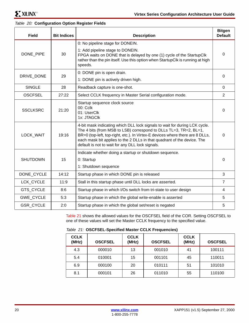
Virtex Series Configuration Architecture User GuideR13
Table 21 shows the allowed values for the OSCFSEL field of the COR Setting OSCFSEL toone of these values will set the Master CCLK frequency to the specified value
Table 20 Configuration Option Register Fields
Field Bit Indices DescriptionBitgenDefault
DONE_PIPE 30
0 No pipeline stage for DONEIN
1 Add pipeline stage to DONEINFPGA waits on DONE that is delayed by one (1) cycle of the StartupClkrather than the pin itself Use this option when StartupClk is running at highspeeds
0
DRIVE_DONE 290 DONE pin is open drain
1 DONE pin is actively driven high0
SINGLE 28 Readback capture is one-shot 0
OSCFSEL 2722 Select CCLK frequency in Master Serial configuration mode 2
SSCLKSRC 2120
Startup sequence clock source00 Cclk01 UserClk1x JTAGClk
0
LOCK_WAIT 1916
4-bit mask indicating which DLL lock signals to wait for during LCK cycleThe 4 bits (from MSB to LSB) correspond to DLLs TL=3 TR=2 BL=1BR=0 (top-left top-right etc) In Virtex-E devices where there are 8 DLLseach mask bit applies to the 2 DLLs in that quadrant of the device Thedefault is not to wait for any DLL lock signals
0
SHUTDOWN 15
Indicate whether doing a startup or shutdown sequence
0 Startup
1 Shutdown sequence
0
DONE_CYCLE 1412 Startup phase in which DONE pin is released 3
LCK_CYCLE 119 Stall in this startup phase until DLL locks are asserted 7
GTS_CYCLE 86 Startup phase in which IOs switch from tri-state to user design 4
GWE_CYCLE 53 Startup phase in which the global write-enable is asserted 5
GSR_CYCLE 20 Startup phase in which the global setreset is negated 5
Table 21 OSCFSEL-Specified Master CCLK Frequencies)
CCLK(MHz) OSCFSEL
CCLK(MHz) OSCFSEL
CCLK(MHz) OSCFSEL
43 000010 13 001010 41 100111
54 010001 15 001101 45 110011
69 000100 20 010111 51 101010
81 000101 26 011010 55 110100
20 wwwxilinxcom XAPP151 (v15) September 27 20001-800-255-7778
Virtex Series Configuration Architecture User GuideR13
Table 22 shows the values of the DONE_CYCLE LCK_CYCLE GTS_CYCLE GWE_CYCLEand GSR_CYCLE fields in COR This table shows the step in the start-up sequence when eachof these signals becomes active
Control Register (CTL)The Control Register (CTL) fields are illustrated in Figure 16 on page 21 and defined inTable 23
92 000110 30 011101 60 101101
100 000111 34 110010 mdash mdash
Notes1 These values are accurate to +45 ndash 30
Table 22 COR Startup Cycle Fields
FieldValue
DONE_CYCLE(DONE Active)
GTS_CYCLE(GTS_CFGInactive)
GSR_CYCLE(GSR Inactive)
GWE_CYCLE(GWE Active) LCK_CYCLE
000 1 1 1 1 0
001 2 2 2 2 1
010 3 3 3 3 2
011 4 (default) 4 4 4 3
100 5 5 (default) 5 5 4
101 6 6 6 (default) 6 (default) 5
110 mdash DoneIndagger DoneIndagger DoneIndagger 6
111 Keep State Keep State Keep State Keep State Donrsquot Wait(default)
Notes1 dagger DONE if DonePipe = No else the delayed version of DONE
Table 21 OSCFSEL-Specified Master CCLK Frequencies) (Continued)
CCLK(MHz) OSCFSEL
CCLK(MHz) OSCFSEL
CCLK(MHz) OSCFSEL
SB
ITS
PE
RS
IST
GT
S_U
SR
_B
31 30 29 28 27 26 25 24 23 22 21 20 19 18 17 16 15 14 13 12 11 10 9 8 7 6 5 4 3 2 1 00 0 0 0 0 0 0 0 0 0 0 0 0 0 0 0 0 0 0 0 0 0 0 x x x 0 0 0 0 0 x
Notes1 Locations within fields containing a zero or one must have these values An X in a bit field indicates that the value is variable and must
be set2 Heavy vertical lines are used to separate fields Light vertical lines separate nibbles in the word
Figure 16 Control Register Fields
XAPP151 (v15) September 27 2000 wwwxilinxcom 211-800-255-7778
Virtex Series Configuration Architecture User GuideR13
Cyclic Redundancy Check (CRC)A data input error checking mechanism is provided through the Cyclic Redundancy Check(CRC) register When data is written to any configuration register (except LOUT) a 16-bit CRCvalue is calculated using both the register data and the address This value is saved in the CRCregister At the end of any series of writes a pre-calculated CRC block-check value may bewritten to the CRC register If the resulting value is non-zero an error is indicated TheCRC_ERROR bit is accessible through the status register If a CRC error is detectedconfiguration logic is put in the ERROR mode The following section is an algorithm forcomputing CRC
CRC Algorithm Initialization bcc = 0skip_pad = truemore_words = true Check for write operation do
w = next_wordif (w[3127] == rsquo00101rsquo)
A Read OP Donrsquot use in CRCwc = w[100]if (wc == 0)
w = next_wordwc = w[190]
while (wc-- gt 0)
w = next_word
elsif (w[3127] == rsquo00110rsquo)
A Write OP Use in CRC addr = w[1613]if (addr Π0124569DB)
wc = w[100]if (wc == 0)
wc is in next word w = next_wordwc = w[190]
while (wc-- gt 0)
w = next_wordsw[350] = addr wordfor (i=0 ilt36 i++)
Table 23 Control Register Bits
NameBit
Indices Description
SBITS 87 Security level0 ReadWrite OK (default)1 Readback disabled23 Readback disabled Writing disabled except CRCregister
PERSIST 6 Configuration interface remains after configuration0 No (default)1 Yes
GTS_USR_B 0 Active-low global tristate IOs Turn off pull-ups ifGTS_CFG_B is also asserted
22 wwwxilinxcom XAPP151 (v15) September 27 20001-800-255-7778
Virtex Series Configuration Architecture User GuideR13
x16 = bcc[15] XOR sw[i]x15 = bcc[14] XOR x16x2 = bcc[1] XOR x16bcc[150] =
x15bcc[132]x2bcc[0]x16 Note the bit order crc[150] = bcc[015]
else
Pad word - ignore
while (more_words)
Frame Address Register (FAR)The Frame Address Register (FAR) holds the address of the current frame The address isdivided into three parts the block type the major address and the minor address The blocktype field indicates whether the CLB or block RAM address space is used The command in thecommand register is executed each time the FAR is loaded with a new value
The major address selects the CLB or RAM column the minor address selects the frame withinthe column The minor address is incremented each time a full data frame is read from orwritten to the frame data register If the last frame within the CLB column is selected when theincrement occurs the major address is incremented and the minor address is reset to zerootherwise the minor address is incremented However the block RAM major address is notincremented automatically
See Figure 18 for the definitions of valid values for the block type field The FAR field definitionsare shown in Figure 19
Figure 17 CRC Calculation Register
Note the Block RAM Major Address is not incremented automatically To address a differentBlock RAM Content column the FAR must be loaded with the new Major Address
Type CodesCLB 00RAM 01
Figure 18 Block Type Codes
x151_17_021100
15141312111098765432
1013
01234526272829303101
Address 32-bit Data Word
CRC Calculation Register
CRC Data Input Register
CRC Register [310]
DATA_IN
SHIFT
23
16-bit CRC13150
0000 0000 0000 0000133116
1313
XAPP151 (v15) September 27 2000 wwwxilinxcom 231-800-255-7778
Virtex Series Configuration Architecture User GuideR13
Frame Data Input Register (FDRI)The Frame Data Input Register (FDRI) is used to load configuration frame data into a Virtexdevice
The Frame Data Register (FDR) is a shift register into which data is loaded prior to transfer tothe configuration memory Configuration data is written to the Virtex device by loading thecommand register with the WCFG command and then loading the FDR with at least two framesof 32-bit words
The write operation is pipelined such that the first frame of data is written to the configurationmemory while the second frame is being shifted in The last frame (the pad frame) is alwaysdummy data which is not actually written to the configuration memory Each frame write mustinclude enough 32 bit data words to load the frame fully There is one pad word at the end ofeach frame which is required for the pipelining hardware
Frame Data Output Register (FDRO)The Frame Data Output Register (FDRO) is for reading configuration data or captured datafrom the Virtex device a process called readback Readback is performed by loading thecommand register with the RCFG command and then addressing the FDRO with a readcommand
Frame Length Register (FLR)Near the beginning of the configuration bitstream the Frame Length Register (FLR) is writtenwith the length of a frame as measured in 32-bit words This length count is used to providesequencing information for the configuration read and write operations Note that the FLR mustbe written before any FDR operation works It is not necessary to set the FLR more than onceIf the number of bits in a frame is not evenly divisible by 32 the length count of the frame mustbe rounded up to the next highest integer The values for the FLR for all the current Virtexseries devices are given in Table 24
BlockType
Major Address(Column Address)
Minor Address(Frame Address)
31 30 29 28 27 26 25 24 23 22 21 20 19 18 17 16 15 14 13 12 11 10 9 8 7 6 5 4 3 2 1 00 0 0 0 0 x x x x x x x x x x x x x x x x x x 0 0 0 0 0 0 0 0 0
Notes1 Locations within fields containing a zero or one must have these values An X in a bit field indicates that the value is variable and must
be set2 Heavy vertical lines are used to separate fields Light vertical lines separate nibbles in the word
Figure 19 Frame Address Fields (FAR)
Note The FLR contains a value that is one less than the number of words that are read fromor written to a given frame This is because the extra word needed for pipelining is not counted
Table 24 Frame Length Register Value
Device Row times Col Frame Length Words per Frame FLR Value
XCV50E 16 times 24 384 12 11
XCV100E 20 times 30 448 14 13
XCV150 24 times 36 512 16 15
XCV200E 28 times 42 576 18 17
XCV300E 32 times 48 672 21 20
24 wwwxilinxcom XAPP151 (v15) September 27 20001-800-255-7778
Virtex Series Configuration Architecture User GuideR13
Legacy Output Register (LOUT)The Legacy Output Register (LOUT) is used for daisy chaining the configuration bitstream toother Xilinx devices Data written to the LOUT is serialized and appears on the DOUT pin
Mask Register (MASK)The Mask Register (MASK) is a mask register for writes to the CTL register A 1 in bit N of themask allows that bit position to be written in the CTL register The default value of the mask isall 0s
Status Register (STAT)The Status Register (STAT) is loaded with current values of several control or status signalsThe register can be read via the re-configuration block or via JTAG The fields in the Statusregister are illustrated in Figure 20 The values of the signals given in Table 25 on page 26 canbe read from the status register
XCV400E 40 times 60 800 25 24
XCV405E 40 times 60 800 25 24
XCV600E 48 times 72 960 30 29
XCV800 56 times 84 1088 34 33
XCV812E 56 times 84 1088 34 33
XCV1000E 64 times 96 1248 39 38
XCV1600E 72 times 108 1376 43 42
XCV2000E 80 times 120 1536 48 47
XCV2600E 92 times 138 1728 54 53
XCV3200E 104 times 156 1952 61 60
Table 24 Frame Length Register Value (Continued)
Device Row times Col Frame Length Words per Frame FLR Value
DO
NE
INIT
MO
DE
GH
IGH
_B
GS
R_B
GW
E_B
GT
S_C
FG
IN_E
RR
OR
LOC
K
CR
C_E
RR
OR
31 30 29 28 27 26 25 24 23 22 21 20 19 18 17 16 15 14 13 12 11 10 9 8 7 6 5 4 3 2 1 00 0 0 0 0 0 0 0 0 0 0 0 0 0 0 0 0 x x x x x x x x x x x x x x x
Notes1 An X in a bit field indicates that the value is variable2 Heavy vertical lines are used to separate fields Light vertical lines separate nibbles in the word
Figure 20 Status Register Fields
XAPP151 (v15) September 27 2000 wwwxilinxcom 251-800-255-7778
Virtex Series Configuration Architecture User GuideR13
ConfigurationInterface
There are two configuration interfaces to the Virtex devices mdash the bit-serial Boundary Scaninterface and the 8-bit byte-serial SelectMAP interface Conceptually XCV50 configurationdata appears as in Figure 21
Frames and words within frames are written in the same order in both configuration interfacesstarting with Frame 0 word 0 (the left-most in the picture) followed by word 1 etc Bits withineach word are written from left to right (MSB first) in the bit-serial configuration interfaces
Within the SelectMAP interface data is written a byte at a time A sample word is shown inFigure 22 The top row indicates the device pin names The bottom row indicates the bit indiceswithin a configuration word Byte 0 loads first followed by byte 1 et cetera The MSB of eachbyte (ie bits 31 23 15 and 7) is loaded on pin D0 The LSB of each byte (ie bits 24 16 8and 0) is loaded on pin D7
PartialReconfigurationof CLBs
Partial reconfiguration can be performed with and without shutting down the device Ifcontention occurs it is advised to go through a shutdown sequence prior to loadingconfiguration frames When shutting down the DONE pin will go active and pull low If this is notdesireable the DONE pin can be prevented from going low by selecting the DONE_CYCLE toKeep State (111) Similarly to prevent GSR from becoming active and reseting the currentstate the GSR_CYCLE can be set to Keep State When not shutting down changes occurframe by frame but is completely done by the end of the Last Frame packet (see Example 1)
Table 25 Status Register Bits
Name Bit Indices Description
DONE 14 Input from DONE pin
INIT 13 Value of INIT
MODE 1210 Value of M2 M1 M0 mode pins
GHIGH_B 9 0 = GHIGH_B asserted
GSR_B 8 0 = all flip-flops are ResetSet
GWE_B 7 1 = flip-flops and block RAM are write disabled
GTS_CFG 6 0 = IOs are tri-stated
IN_ERROR 5 Legacy input error
LOCK 41 Output from DLL lock signals 1 = DLL is locked
CRC_ERROR 0 Indicates that a CRC error has occurred
Data Frame 0 (11 words) Pad Word
hellip
Data Frame n (11 words) Pad WordPad Frame (12 words)
Figure 21 XCV50 Frame Padding for Reads
Figure 22 SelectMAP Byte and Bit Ordering
x151_22_021100
D0 D1 D2 D3 D4 D5 D6 D7 D0 D1 D2 D3 D4 D5 D6 D7 D0 D1 D2 D3 D4 D5 D6 D7 D0 D1 D2 D3 D4 D5 D6 D7
Byte 0 Byte 1 Byte 2 Byte 313
26 wwwxilinxcom XAPP151 (v15) September 27 20001-800-255-7778
Virtex Series Configuration Architecture User GuideR13
The DONE pin will not change in this case Figure 23 illustrates a typical shutdownreconfiguration in the CLB address space and restart sequence
Examples Several examples of reading and evaluating configuration data are provided to illustrate thefollowing
Figure 23 Typical Shutdown Reconfiguration in the CLB Address Spaceand Restart Sequence
FFFF FFFF Dummy WordAA99 5566 Sync Word Does not realign an already synchronized SelectMap port3001 2001 COR0080 FF2F Shutdown bit set optionally set bit 29 DRIVE_DONE
Alternately COR may be read bit 15 set and written back3000 8001 CMD0000 0005 Start Shutdown3000 8001 CMD0000 0007 Reset CRC0000 00000000 0000 Clock shutdown sequence0000 00000000 00003000 8001 CMD0000 0008 Assert GHIGH3000 8001 CMD0000 0001 Write Configuration3000 2001 FAR0--- ---- Block Type CLB (00) MajorMinor Address3000 4--- FDRI + Word Count if count is lt1024 Otherwise use TypeII Header
Write FRAME DATAIf CLB Frames are not written to non-consecutive addresses repeat FAR word followedby new MajorMinor Address followed by FDRI + Word Count and then Frame Data
3000 0001 Write CRC---- ---- CRC3000 8001 CMD0000 0003 LFRM3000 4--- FDRI + Word Count
Write PAD FRAME
3001 2001 COR0080 3F2D Default COR Options
Alternately COR may be read bit 15 cleared and written back3000 8001 CMD0000 0005 Begin Startup3000 0001 Write CRC---- ---- CRC
0000 00000000 0000 4 Dummy Words0000 00000000 0000
Example 1 Read and Write Semaphores in an XCV100 at CLB R1 C1 Slice 0 on page 28Example 2 Reading the Complete Configuration from an XCV50 on page 33
XAPP151 (v15) September 27 2000 wwwxilinxcom 271-800-255-7778
Virtex Series Configuration Architecture User GuideR13
Example 1 Read and Write Semaphores in an XCV100 at CLB R1 C1Slice 0Semaphores are a useful communication mechanism documented in XAPP 153 ldquoStatus andControl Semaphore Registers using Partial Reconfigurationrdquo Figure 24 shows an abstractionof a microprocessor writing control information to an FPGA and reading status informationOne convention for implementing semaphores in Virtex devices is to use two bits of a 16-bitdual-port RAM as illustrated in Figure 25 This occupies one CLB slice with the F-LUTimplementing the control semaphore and the status semaphore implemented in the G-LUTAddress 15 of the G-LUT is used for on-chip writes to the semaphore and address 14 of the F-LUT is used for on-chip reads Conversely the off-chip microprocessor is reading the G-LUT[15] and writing F-LUT[14]
Example 3 Read the Slice 0 G-LUT from CLB R1 C1 from the Complete Configuration of anXCV50 on page 34Example 4 Read the Slice 1 F-LUT from CLB R19 C16 from an XCV100 on page 36Example 5 Read All Bits in Slice 0 G-LUTs from CLB C2 and XCV50 on page 39Example 6 Read Block SelectRAM index 387 of RAM R2 C0 from an XCV100E on page 41
Figure 24 Semaphore Abstraction
x151_ 23_021400
Status13
Control13
MicroProcessor FPGA13
Semaphores13
28 wwwxilinxcom XAPP151 (v15) September 27 20001-800-255-7778
Virtex Series Configuration Architecture User GuideR13
Using a Semaphore Abstraction dual-port RAM ensures that the LUT SelectRAMs are placedin the CLB in a predictable manner When writing data to one or more LUT SelectRAMs or flip-flops on the device all bits in the frame must have valid configuration information This isassured by altering valid configurations from bitstream files or from frames read from a properlyconfigured Virtex device The latter approach is used in this example
Figure 25 Semaphore ReadWrite Implementation
Frame 47
15
14
47 46
47 46
x151_ 24_021100
Select Map
Frame 46
DING
F
13
D2D3D4 5D6 7D0D1 D D
1
111
0
111
Chip Interface
G F
13
XAPP151 (v15) September 27 2000 wwwxilinxcom 291-800-255-7778
Virtex Series Configuration Architecture User GuideR13
Attributes for this design are summarized in Table 26
From the equations in Table 7 on page 11 the values shown in Table 27 can be calculated
From off-chip for reading the G-LUT[15] bit read one frame (MNA=47) For writing the F-LUT[14] bit we show how to read then write one frame (MNA=46) as opposed to modifyingdata from a bitstream file (both are valid methods) The frames on the XCV100 contain 13 32-bit words and one pad word Remember that fm_st_wd is calculated assuming the entireconfiguration has been read However only the pad frame and then frames 46 and 47 fromMajor Address 30 are being read The desired bit is in Frame 1 word 1 which is word 15
The commands for reading both frames (and the pad frame) are given in Figure 26
Table 26 Design Attributes for Example 1
Attribute
G-LUT [15] F-LUT [14]
Read Read Write
Chip_Rows 20
Chip_Cols 30
FL 14
CLB_Row 1
CLB_Col 1
Slice 0
FG 1 0
lut_bit 15 14
RW 1 1 0
Table 27 Semaphore Example Variables Equations and Values
Variable Equation
Value(s)
G-LUT[15] F-LUT[14]
Read Read Write
MJA 1 le 302 rArr 30 ndash 1 times 2 + 2 30
MNA lut_bit + 32ndash 0 times () 47 46
fm_bit_idx 3 + 18 times 1 ndash FG + RW times 32 52 53 21
fm_st_wd 14 times (8 + (30 ndash 1) times 48+ 4647) +RW times (14 +1)= 14 times (1400 + 4647) + 14 times RW= 19600 + 14 times 4647 + 14 times RW
20272 20258 20244
fm_wd floor (2032) 1 1 0
fm_wd_bit_idx 31 + 32 times 110 ndash 525321 11 10 10
30 wwwxilinxcom XAPP151 (v15) September 27 20001-800-255-7778
Virtex Series Configuration Architecture User GuideR13
The 42 words read are shown in Figure 27 F-LUT[14] is in the second frame (frame=1word=1) at bit 10 The value read is a 1 but because the LUT bits are inverted the logic valueis zero G-LUT[15] is in word one of the third data frame (frame=2 word=1) at bit 11The valueread is a 1 which is a logic zero
InstructionData
Hex 31 30 29 28 27 26 25 24 23 22 21 20 19 18 17 16 15 14 13 12 11 10 9 8 7 6 5 4 3 2 1 0
Sync Word AA99 5566 1 0 1 0 1 0 1 0 1 0 0 1 1 0 0 1 0 1 0 1 0 1 0 1 0 1 1 0 0 1 1 0
Write next (1) word to FAR 3000 2001 0 0 1 1 0 0 0 0 0 0 0 0 0 0 0 0 0 0 1 0 0 0 0 0 0 0 0 0 0 0 0 1
CLB MJA=30 MNA=46 003C 5800 0 0 0 0 0 0 0 0 0 0 1 1 1 1 0 0 0 1 0 1 1 1 0 0 0 0 0 0 0 0 0 0
Write next word to CMD 3000 8001 0 0 1 1 0 0 0 0 0 0 0 0 0 0 0 0 1 0 0 0 0 0 0 0 0 0 0 0 0 0 0 1
Register value for RCFG 0000 0004 0 0 0 0 0 0 0 0 0 0 0 0 0 0 0 0 0 0 0 0 0 0 0 0 0 0 0 0 0 1 0 0
Read from FDRO 2800 602A 0 0 1 0 1 0 0 0 0 0 0 0 0 0 0 0 0 1 1 0 0 0 0 0 0 0 1 0 1 0 1 0
Flush pipe 0000 0000 0 0 0 0 0 0 0 0 0 0 0 0 0 0 0 0 0 0 0 0 0 0 0 0 0 0 0 0 0 0 0 0
(read 42 words)
Notes1 Binary data is grouped in two ways for ease of interpretation Thin vertical lines separate nibble boundaries Heavy vertical lines
separate field boundaries
Figure 26 Commands to Read Two Data Frames
XAPP151 (v15) September 27 2000 wwwxilinxcom 311-800-255-7778
Virtex Series Configuration Architecture User GuideR13
To write to the F-LUT semaphore start with the second data frame (frame=1) that was justread Words 1 - 13 of that frame will become words 0 - 12 of the frame to be written Word 13of this new frame is a pad word and can have any value (typically 0 is chosen) In this newframe set bit 11 of word 0 (zero) to the desired value of the semaphore A pad frame mustfollow the data frame The commands from Figure 28 write these two frames into the device atthe proper location
Frame Word 31 30 29 28 27 26 25 24 23 22 21 20 19 18 17 16 15 14 13 12 11 10 9 8 7 6 5 4 3 2 1 0
0
0 1 1 1 1 1 1 1 1 1 1 1 1 1 1 1 1 1 1 1 1 1 1 1 1 1 1 1 1 1 1 1 1
1 1 1 1 1 1 1 1 1 1 1 1 1 1 1 1 1 1 1 1 1 1 1 1 1 1 1 1 1 1 1 1 1
2 1 1 1 1 1 1 1 1 1 1 1 1 1 1 1 1 1 1 1 1 1 1 1 1 1 1 1 1 1 1 1 1
3 1 1 1 1 1 1 1 1 1 1 1 1 1 1 1 1 1 1 1 1 1 1 1 1 1 1 1 1 1 1 1 1
4 1 1 1 1 1 1 1 1 1 1 1 1 1 1 1 1 1 1 1 1 1 1 1 1 1 1 1 1 1 1 1 1
5 1 1 1 1 1 1 1 1 1 1 1 1 1 1 1 1 1 1 1 1 1 1 1 1 1 1 1 1 1 1 1 1
6 1 1 1 1 1 1 1 1 1 1 1 1 1 1 1 1 1 1 1 1 1 1 1 1 1 1 1 1 1 1 1 1
7 1 1 1 1 1 1 1 1 1 1 1 1 1 1 1 1 1 1 1 1 1 1 1 1 1 1 1 1 1 1 1 1
8 1 1 1 1 1 1 1 1 1 1 1 1 1 1 1 1 1 1 1 1 1 1 1 1 1 1 1 1 1 1 1 1
9 1 1 1 1 1 1 1 1 1 1 1 1 1 1 1 1 1 1 1 1 1 1 1 1 1 1 1 1 1 1 1 1
10 1 1 1 1 1 1 1 1 1 1 1 1 1 1 1 1 1 1 1 1 1 1 1 1 1 1 1 1 1 1 1 1
11 1 1 1 1 1 1 1 1 1 1 1 1 1 1 1 1 1 1 1 1 1 1 1 1 1 1 1 1 1 1 1 1
12 1 1 1 1 1 1 1 1 1 1 1 1 1 1 1 1 1 1 1 1 1 1 1 1 1 1 1 1 1 1 1 1
13 1 1 1 1 1 1 1 1 1 1 1 1 1 1 1 1 1 1 1 1 1 1 1 1 1 1 1 1 1 1 1 1
1
0 0 0 0 0 0 0 0 0 0 0 0 0 0 0 0 0 0 0 0 0 0 0 0 0 0 0 0 0 0 0 0 0
1 1 0 0 0 0 0 0 0 0 0 0 0 1 0 0 0 0 1 1 0 1 1 0 0 0 0 0 0 0 0 0 0 F[14]
2 1 1 1 1 1 0 1 1 0 0 0 0 1 1 1 1 0 0 1 1 1 1 1 0 1 1 0 0 0 0 0 0
3 0 0 0 0 1 1 1 1 1 0 1 1 0 0 0 0 0 0 0 0 0 0 1 1 1 1 1 0 1 1 0 0
4 0 0 0 0 0 0 0 0 1 1 1 1 0 0 0 0 0 0 0 0 0 0 0 0 0 0 1 1 1 1 1 0
5 1 1 0 0 1 1 0 0 0 0 0 0 1 1 0 0 1 0 1 1 0 0 0 0 0 0 0 0 0 0 1 1
6 1 1 1 0 1 1 0 0 0 0 0 0 1 1 1 0 1 1 1 0 1 0 1 1 0 0 0 0 0 0 0 0
7 0 0 1 1 1 1 1 0 1 1 0 0 0 0 1 1 0 0 0 0 1 1 1 1 1 0 1 1 0 0 0 0
8 0 0 0 0 0 0 1 1 1 1 1 0 0 0 0 0 0 0 0 0 0 0 0 0 1 1 1 1 1 0 1 1
9 0 0 0 0 0 0 0 0 0 0 1 1 0 0 0 0 1 1 0 0 0 0 0 0 0 0 0 0 1 1 1 1
10 1 0 1 1 0 0 0 0 0 0 0 0 1 0 1 1 1 1 1 0 1 1 0 0 0 0 0 0 0 0 0 0
11 1 1 1 1 1 0 1 1 0 0 0 0 1 1 1 1 0 0 1 1 1 1 1 0 1 1 0 0 0 0 0 0
12 0 0 0 0 1 1 0 1 1 0 1 1 0 0 0 0 0 0 0 0 0 0 1 1 1 1 1 0 0 0 0 0
13 0 0 0 0 0 0 1 1 0 1 0 1 0 0 0 0 0 0 0 0 0 0 0 0 0 0 0 0 0 0 0 0
2
0 0 0 0 0 0 0 0 0 0 0 0 0 0 0 0 0 0 0 0 0 0 0 0 0 0 0 0 0 0 0 0 0
1 1 0 1 0 0 0 0 0 0 0 0 1 1 0 1 0 1 1 1 0 1 1 0 0 0 0 0 0 0 0 0 0 G[15]
2 1 1 1 1 1 1 1 1 0 0 0 0 1 1 1 1 0 0 1 1 1 1 1 1 1 1 0 0 0 0 0 0
3 0 0 0 0 1 1 1 1 1 1 1 1 0 0 0 0 0 0 0 0 0 0 1 0 1 1 1 1 1 1 0 0
4 0 0 0 0 0 0 0 0 1 1 1 1 0 0 0 0 0 0 0 0 0 0 0 0 0 0 1 1 1 1 1 1
5 1 1 0 0 0 0 0 0 0 0 0 0 1 1 0 0 1 1 1 1 0 0 1 0 0 0 0 0 0 0 1 1
6 1 1 1 1 1 1 0 0 0 0 0 0 1 1 1 1 1 1 1 1 1 1 1 1 0 0 0 0 0 0 0 0
7 0 0 1 1 1 1 1 1 1 1 0 0 0 0 1 1 0 0 0 0 1 1 1 1 1 1 1 1 0 0 0 0
8 0 0 0 0 0 0 1 1 1 1 1 1 0 0 0 0 0 0 0 0 0 0 0 0 1 1 1 1 1 1 1 1
9 0 0 0 0 0 0 0 0 0 0 1 1 0 0 0 0 1 1 0 0 0 0 0 0 0 0 0 0 1 1 1 1
10 1 1 1 1 0 0 0 0 0 0 0 0 1 1 1 1 1 1 1 1 1 1 0 0 0 0 0 0 0 0 0 0
11 1 1 1 1 1 1 1 1 0 0 0 0 1 1 1 1 0 0 1 1 1 1 1 1 1 1 0 0 0 0 0 0
12 0 0 0 0 1 1 0 1 1 1 1 1 0 0 0 0 0 0 0 0 0 0 1 1 1 1 1 0 1 0 0 0
13 0 0 0 0 0 1 1 0 0 1 1 1 0 0 0 0 0 0 0 0 0 0 0 0 0 0 0 0 0 0 0 0
Figure 27 Three Frames Containing the Semaphores
32 wwwxilinxcom XAPP151 (v15) September 27 20001-800-255-7778
Virtex Series Configuration Architecture User GuideR13
Example 2 Reading the Complete Configuration from an XCV50Steps
1 If flip-flop values are needed clock the on-chip signal CAPTURE to capture flip-flopvalues See the Xilinx Libraries Guide for use of the CAPTURE_VIRTEX cell
2 Write the starting frame address (CLB MJA=0 MNA=0) into the FAR
3 Write the RCFG command to the CMD register
4 Address the FDRO register with a READ operation and word count equal to the number of32-bit words in the CLB frames plus one pad frame
5 Read the data following the timing diagrams in the SelectMAP interface section
6 Write the address for RAM block 0 to the FAR
7 Address the FDRO register with a read operation and word count equal to the number of32-bit words in the RAM block plus one pad frame
8 Read the data
9 Write the address for RAM block 1 to the FAR
10 Address the FDRO register with a read operation and word count equal to the number of32-bit words in the RAM block plus one pad frame
11 Read the data
When using SelectMAP mode to read data words from the Virtex device de-assert CS de-assert WRITE assert CS then clock the data out When using JTAG load the JTAG IR
InstructionData
Hex 31 30 29 28 27 26 25 24 23 22 21 20 19 18 17 16 15 14 13 12 11 10 9 8 7 6 5 4 3 2 1 0
Sync Word AA995566
1 0 1 0 1 0 1 0 1 0 0 1 1 0 0 1 0 1 0 1 0 1 0 1 0 1 1 0 0 1 1 0
Write next (1) word to FAR 30002001
0 0 1 1 0 0 0 0 0 0 0 0 0 0 0 0 0 0 1 0 0 0 0 0 0 0 0 0 0 0 0 1
MJA=30 MNA=46 003C5C00
0 0 0 0 0 0 0 0 0 0 1 1 1 1 0 0 0 1 0 1 1 1 0 0 0 0 0 0 0 0 0 0
Write next word to CMD 30008001
0 0 1 1 0 0 0 0 0 0 0 0 0 0 0 0 1 0 0 0 0 0 0 0 0 0 0 0 0 0 0 1
Register value for WCFG 00000001
0 0 0 0 0 0 0 0 0 0 0 0 0 0 0 0 0 0 0 0 0 0 0 0 0 0 0 0 0 0 0 1
Write 28 words to FDRI 3000401C
0 0 1 1 0 0 0 0 0 0 0 0 0 0 0 0 0 1 0 0 0 0 0 0 0 0 0 1 1 1 0 0
Data Word 0 A01AEC00
1 0 1 0 0 0 0 0 0 0 0 1 1 0 1 0 1 1 1 0 1 1 0 0 0 0 0 0 0 0 0 0
Data Word 1 FF0F3FC0
1 1 1 1 1 1 1 1 0 0 0 0 1 1 1 1 0 0 1 1 1 1 1 1 1 1 0 0 0 0 0 0
Data Word 2 0FF002FC
0 0 0 0 1 1 1 1 1 1 1 1 0 0 0 0 0 0 0 0 0 0 1 0 1 1 1 1 1 1 0 0
hellip hellip hellip
Data Word 27 00000000
0 0 0 0 0 0 0 0 0 0 0 0 0 0 0 0 0 0 0 0 0 0 0 0 0 0 0 0 0 0 0 0
Notes1 Binary data is grouped in two ways for ease of interpretation Thin vertical lines separate nibble boundaries Heavy
vertical lines separate field boundaries
Figure 28 Commands to Write a Semaphore Value
XAPP151 (v15) September 27 2000 wwwxilinxcom 331-800-255-7778
Virtex Series Configuration Architecture User GuideR13
(instruction register) with the CFG_OUT instruction Then go to the SDR (Shift-DR) state andshift the data out (See Figure 29)
Example 3 Read the Slice 0 G-LUT from CLB R1 C1 from the CompleteConfiguration of an XCV50The commands for reading the bitstream from the Virtex device are given in Example 1 Readand Write Semaphores in an XCV100 at CLB R1 C1 Slice 0 on page 28 Using an XCV50device the independent attributes are show in Table 28
InstructionData
Hex 31 30 29 28 27 26 25 24 23 22 21 20 19 18 17 16 15 14 13 12 11 10 9 8 7 6 5 4 3 2 1 0
Sync Word AA99 5566 1 0 1 0 1 0 1 0 1 0 0 1 1 0 0 1 0 1 0 1 0 1 0 1 0 1 1 0 0 1 1 0
Write next word to FAR 3000 2001 0 0 1 1 0 0 0 0 0 0 0 0 0 0 0 0 0 0 1 0 0 0 0 0 0 0 0 0 0 0 0 1
CLB MJA=0 MNA=0 0000 0000 0 0 0 0 0 0 0 0 0 0 0 0 0 0 0 0 0 0 0 0 0 0 0 0 0 0 0 0 0 0 0 0
Write next word to CMDregister
3000 8001 0 0 1 1 0 0 0 0 0 0 0 0 0 0 0 0 1 0 0 0 0 0 0 0 0 0 0 0 0 0 0 1
Register value for RCFG 0000 0004 0 0 0 0 0 0 0 0 0 0 0 0 0 0 0 0 0 0 0 0 0 0 0 0 0 0 0 0 0 1 0 0
Read from FDRO register 2800 6000 0 0 1 0 1 0 0 0 0 0 0 0 0 0 0 0 0 1 1 0 0 0 0 0 0 0 0 0 0 0 0 0
15876 words 4800 3E04 0 1 0 0 1 0 0 0 0 0 0 0 0 0 0 0 0 0 1 1 1 1 1 0 0 0 0 0 0 1 0 0
Flush pipe 0000 0000 0 0 0 0 0 0 0 0 0 0 0 0 0 0 0 0 0 0 0 0 0 0 0 0 0 0 0 0 0 0 0 0
(Read 15876 words)Write to FAR register 3000 2001 0 0 1 1 0 0 0 0 0 0 0 0 0 0 0 0 0 0 1 0 0 0 0 0 0 0 0 0 0 0 0 1
RAM MJA=0 MNA=0 0200 0000 0 0 0 0 0 0 1 0 0 0 0 0 0 0 0 0 0 0 0 0 0 0 0 0 0 0 0 0 0 0 0 0
Read 780 words fromFDRO reg
2800 630C 0 0 1 0 1 0 0 0 0 0 0 0 0 0 0 0 0 1 1 0 0 0 1 1 0 0 0 0 1 1 0 0
Flush pipe 0000 0000 0 0 0 0 0 0 0 0 0 0 0 0 0 0 0 0 0 0 0 0 0 0 0 0 0 0 0 0 0 0 0 0
(Read 780 words)Write to FAR register 3000 2001 0 0 1 1 0 0 0 0 0 0 0 0 0 0 0 0 0 0 1 0 0 0 0 0 0 0 0 0 0 0 0 1
RAM MJA=1 MNA=0 0202 0000 0 0 0 0 0 0 1 0 0 0 0 0 0 0 1 0 0 0 0 0 0 0 0 0 0 0 0 0 0 0 0 0
Read 780 words fromFDRO reg
2800 630C 0 0 1 0 1 0 0 0 0 0 0 0 0 0 0 0 0 1 1 0 0 0 1 1 0 0 0 0 1 1 0 0
Flush pipe 0000 0000 0 0 0 0 0 0 0 0 0 0 0 0 0 0 0 0 0 0 0 0 0 0 0 0 0 0 0 0 0 0 0 0
(Read 780 words)
Figure 29 Example 2 - Read Complete Configuration for XCV50
Table 28 XCV50 Independent Attributes
Independent Attributes Values
Chip_Rows 16
Chip_Cols 24
FL 12
CLB_Row 1
CLB_Col 1
FG 1
Slice 0
RW 1
34 wwwxilinxcom XAPP151 (v15) September 27 20001-800-255-7778
Virtex Series Configuration Architecture User GuideR13
From the equations given earlier in Table 7 calculating the range of values for fm_st_wdindicates that the word 13740 of the configuration is the starting word of the 12-word (FL=12)frame containing bit 0 of the G-LUT in Slice 0 of CLB R1C1 (Table 29)
The configuration bits for the given frame are as follows G-LUT[0] is in fm_wd=0 at bit 11
All 16 LUT SelectRAM bits are in the following words at the same bit index 11
Table 29 Variables Equations and Values for Slice 0 G-LUT
Variables Equations Values
MJA 1 le 242 rArr 24 ndash 1times 2 + 2 24
MNA 0 times (hellip) + lut_bit + 32 0 321 332 343 35
4 365 376 387 39
8 409 41
10 4211 43
12 4413 4514 4615 47
fm_bit_idx 3 + 18 times 1 ndash1 + RW times 32 52
fm_st_wd 12 times (8+ (24 ndash1) times 48 + [3247]) +1 x 12= 12 times (1112 + [3247]) +12= 13356 + 12 times 3247]
1374013920
fm_wd floor(5232) 1
fm_wd_bit_idx 31 + 32 ndash 52 11
BitstreamWord
Frame 32-bit Word FrameWord31 30 29 28 27 26 25 24 23 22 21 20 19 18 17 16 15 14 13 12 11 10 9 8 7 6 5 4 3 2 1 0
13740 0 0 0 0 0 0 0 0 0 0 0 0 0 0 0 0 0 0 0 0 0 0 0 0 0 0 0 0 0 0 0 0 013741 0 0 1 0 1 0 0 0 0 0 0 0 0 1 0 1 0 1 0 0 1 1 1 0 0 0 0 0 0 0 0 0 113742 1 0 1 1 0 0 1 1 0 0 0 0 0 0 0 0 0 0 1 0 1 1 0 0 1 1 0 0 0 0 0 0 213743 0 0 0 0 1 0 1 1 0 0 1 1 0 0 0 0 0 0 0 0 0 0 1 0 1 1 0 0 1 1 0 0 313744 0 0 0 0 0 0 0 0 1 0 1 1 0 0 1 1 0 0 0 0 0 0 0 0 0 0 1 0 1 1 0 0 413745 1 1 0 0 0 0 0 0 0 0 0 0 1 0 1 1 0 0 1 1 0 0 0 0 0 0 0 0 0 0 1 0 513746 1 1 0 0 1 1 0 0 0 0 0 0 0 0 0 0 1 0 1 1 0 0 1 1 0 0 0 0 0 0 0 0 613747 0 0 1 0 1 1 0 0 1 1 0 0 0 0 0 0 0 0 0 0 1 0 1 1 0 0 1 1 0 0 0 0 713748 0 0 0 0 0 0 1 0 1 1 0 0 1 1 0 0 0 0 0 0 0 0 0 0 1 0 1 1 0 0 1 1 813749 0 0 0 0 0 0 0 0 0 0 1 0 1 1 0 0 1 1 0 0 0 0 0 0 0 0 0 0 1 0 1 1 913750 0 0 1 1 0 0 0 0 0 0 0 0 0 0 1 0 1 1 0 0 1 0 1 0 0 0 0 0 0 0 0 0 1013751 0 1 0 1 0 0 0 0 0 0 0 0 0 0 0 0 0 0 0 0 0 0 0 0 0 0 0 0 0 0 0 0 11
Figure 30 Configuration Bits for Slice 0 CLB R1C1 G-LUT [0]
XAPP151 (v15) September 27 2000 wwwxilinxcom 351-800-255-7778
Virtex Series Configuration Architecture User GuideR13
The 16 bits are LUT[150]=0111111111111111 The LUT SelectRAM bits are inverted from theirlogic values The ldquologicalrdquo contents are LUT[150]=1000000000000000 Thus this G-LUTimplements a 4-input AND function
Example 4 Read the Slice 1 F-LUT from CLB R19 C16 from an XCV100Commands for reading the bitstream from the Virtex device are given in Figure 32 Use thefollowing independent attributes to find the given F-LUT
From the equations in Table 7 on page 11 calculating fm_st_wd indicates the starting wordwith respect to a configuration that starts at MJA=0 MNA=0 Because the frames we are
BitstreamWord
Frame 32-bit Word
LUT Bit31 30 29 28 27 26 25 24 23 22 21 20 19 18 17 16 15 14 13 12 11 10 9 8 7 6 5 4 3 2 1 0
13741 0 0 1 0 1 0 0 0 0 0 0 0 0 1 0 1 0 1 0 0 1 1 1 0 0 0 0 0 0 0 0 0 0
13753 1 0 1 0 0 0 0 0 0 0 0 0 0 0 0 1 0 0 0 1 1 1 0 0 0 0 0 0 0 0 0 0 1
13765 1 0 1 0 1 0 0 0 0 0 0 0 1 0 0 0 0 0 0 1 1 1 1 0 0 0 0 0 0 0 0 0 2
13777 0 0 0 0 1 0 0 0 0 0 0 1 1 1 0 1 1 0 1 0 1 1 0 0 0 0 0 0 0 0 0 0 3
13789 0 1 0 0 0 0 0 0 0 0 0 0 0 1 0 1 1 1 1 1 1 1 1 0 0 0 0 0 0 0 0 0 4
13801 1 0 1 0 1 0 0 0 0 0 0 1 0 0 0 1 1 0 0 1 1 1 0 0 0 0 0 0 0 0 0 0 5
13813 0 0 0 1 0 0 0 0 0 0 0 0 0 0 0 0 1 0 0 1 1 1 0 0 0 0 0 0 0 0 0 0 6
13825 0 1 1 0 1 0 0 0 0 0 0 1 0 1 0 0 1 1 0 0 1 1 0 0 0 0 0 0 0 0 0 0 7
13837 1 0 1 1 1 0 0 0 0 0 0 1 0 1 0 1 1 0 0 0 1 1 0 0 0 0 0 0 0 0 0 0 8
13849 1 0 0 0 0 0 0 0 0 0 0 0 0 0 0 0 1 1 1 0 1 1 0 0 0 0 0 0 0 0 0 0 9
13861 1 0 0 0 0 0 0 0 0 0 0 1 0 0 0 0 1 1 1 1 1 1 1 0 0 0 0 0 0 0 0 0 10
13873 1 0 0 0 0 0 0 1 0 0 0 0 0 1 0 0 0 1 1 0 1 1 0 0 0 1 0 0 0 0 0 0 11
13885 1 0 0 0 0 0 0 0 0 0 0 0 0 1 0 1 0 0 1 0 1 1 0 0 0 0 0 0 0 0 0 0 12
13897 0 0 0 0 1 0 0 0 0 0 0 0 0 1 0 0 0 0 0 0 1 1 0 0 0 0 0 0 0 0 0 0 13
13909 1 0 0 0 0 0 0 0 0 0 0 0 1 1 0 1 0 1 1 0 1 1 0 0 0 0 0 0 0 0 0 0 14
13921 1 0 1 0 0 0 0 0 0 0 0 1 1 1 0 1 1 1 1 1 0 1 0 0 0 0 0 0 0 0 0 0 15
Figure 31 Location of all 16 LUT SelectRAM Bits
Table 30 Virtex Bitstream Command Attributes
Independent Attributes Values
Chip_Rows 20
Chip_Cols 30
FL 14
CLB_Row 19
CLB_Col 16
FG 0
Slice 1
RW 1
36 wwwxilinxcom XAPP151 (v15) September 27 20001-800-255-7778
Virtex Series Configuration Architecture User GuideR13
interested in start at MJA=1 MNA=0 which is fm_st_wd = 126 so the first 126 words are notneeded (0ndash125) Therefore to find the given Slice 1 F-LUT see Table 31
Sixteen frames need to be read one for each bit in the LUT SelectRAM The bits in LUTSelectRAMs in Slice 1 occur in the opposite order that they do for Slice 0 LUT SelectRAMs
Frames are read sequentially with ascending addresses If read in LUT bit order LUT[0]LUT[1] hellip LUT[15] These are stored in descending addresses which require 16 separateread operations each reading one data frame and one pad frame However if read inascending address order LUT[15] LUT[14] hellip LUT[0] all 16 data frames are read with asingle read operation This requires only one pad frame for all 16 frames Thus it takes lesstime to read ascending frames starting at MJA=1 MNA=0 and finishing with frame MJA=1MNA=15 The frames in the XCV100 contain 14 32-bit words and a single pad wordCommands for reading only the F-LUT data are given in Figure 32
Table 31 Variables Equations and Values for Slice 1 F-LUT
Variables Equations Values
MJA 16 gt 302 rArr 2times16 ndash 30 ndash1 1
MNA lut_bit + 32 ndash Slice times (2 times lut_bit +17)= [015] + 32 ndash (2 times [015] + 17)= 15 ndash [015]
0 151 142 133 12
4 115 106 97 8
8 79 6
10 511 4
12 313 214 115 0
fm_bit_idx 3 + 18 times 19 ndash 0+ 32 377
fm_st_wd 14 times (8 + (1ndash 1) times 48 + [150]) +1 times 14= 14 times (8 + [150]) +14= 126 + 14 times [150]
= 336126
fm_wd floor(37732) 11
fm_wd_bit_idx 31 + 32 times 11 ndash 377 6
XAPP151 (v15) September 27 2000 wwwxilinxcom 371-800-255-7778
Virtex Series Configuration Architecture User GuideR13
The 377th bit of each frame is the bit in the F-LUT This LUT SelectRAM bit is in the framersquosword index 11 bit index 6
The configuration bits for the given frame in Figure 33 are as follows LUT Bit 15 is in MJA=1MNA=0 fm_wd=11 at bit 6
LUT bit 0 is in MJA=1 MNA=15 fm_wd=11 at bit 6
InstructionData
Hex 31 30 29 28 27 26 25 24 23 22 21 20 19 18 17 16 15 14 13 12 11 10 9 8 7 6 5 4 3 2 1 0
Sync Word AA99 5566 1 0 1 0 1 0 1 0 1 0 0 1 1 0 0 1 0 1 0 1 0 1 0 1 0 1 1 0 0 1 1 0
Write next (1) word to FAR 3000 2001 0 0 1 1 0 0 0 0 0 0 0 0 0 0 0 0 0 0 1 0 0 0 0 0 0 0 0 0 0 0 0 1
CLB MJA = 1 MNA = 0 0002 0000 0 0 0 0 0 0 0 0 0 0 0 0 0 0 1 0 0 0 0 0 0 0 0 0 0 0 0 0 0 0 0 0
Write next word to CMD 3000 8001 0 0 1 1 0 0 0 0 0 0 0 0 0 0 0 0 1 0 0 0 0 0 0 0 0 0 0 0 0 0 0 1
Register value for RCFG 0000 0004 0 0 0 0 0 0 0 0 0 0 0 0 0 0 0 0 0 0 0 0 0 0 0 0 0 0 0 0 0 1 0 0
Read from FDRO 2800 60EE 0 0 1 0 1 0 0 0 0 0 0 0 0 0 0 0 0 1 1 0 0 0 0 0 1 1 1 0 1 1 1 0
Flush pipe 0000 0000 0 0 0 0 0 0 0 0 0 0 0 0 0 0 0 0 0 0 0 0 0 0 0 0 0 0 0 0 0 0 0 0
(Read 238 words)
Figure 32 Commands to read Slice 1 F-LUT
Frame WordFrame 32-bit Word
31 30 29 28 27 26 25 24 23 22 21 20 19 18 17 16 15 14 13 12 11 10 9 8 7 6 5 4 3 2 1 0
0 0 0 0 0 0 0 0 0 0 0 0 0 0 0 0 0 0 0 0 0 0 0 0 0 0 0 0 0 0 0 0 0
1 1 1 0 0 0 0 0 0 0 0 0 0 0 1 0 1 1 1 1 1 1 1 0 0 0 0 0 0 0 0 0 0
2 1 1 1 1 1 1 1 1 0 0 0 0 0 0 0 0 0 0 1 1 1 1 1 1 1 1 0 0 0 0 0 0
3 0 0 0 0 1 1 1 1 1 1 1 1 0 0 0 0 0 0 0 0 0 0 1 1 1 1 1 1 1 1 0 0
4 0 0 0 0 0 0 0 0 1 1 1 1 1 1 1 1 0 0 0 0 0 0 0 0 0 0 1 1 1 1 1 1
5 1 1 0 0 0 0 0 0 0 0 0 0 1 1 1 1 1 1 1 1 0 0 0 0 0 0 0 0 0 0 1 1
6 1 1 1 1 1 1 0 0 0 0 0 0 0 0 0 0 1 1 1 1 1 1 1 1 0 0 0 0 0 0 0 0
7 0 0 1 1 1 1 1 1 1 1 0 0 0 0 0 0 0 0 0 0 1 1 1 1 1 1 1 1 0 0 0 0
8 0 0 0 0 0 0 1 1 1 1 1 1 1 1 0 0 0 0 0 0 0 0 0 0 1 1 1 1 1 1 1 1
9 0 0 0 0 0 0 0 0 0 0 1 1 1 1 1 1 1 1 0 0 0 0 0 0 0 0 0 0 1 1 1 1
10 1 1 1 1 0 0 0 0 0 0 0 0 0 0 1 1 1 1 1 1 1 1 0 0 0 0 0 0 0 0 0 0
11 1 1 1 1 1 1 1 1 0 0 0 0 0 0 0 0 0 0 1 1 1 1 1 1 1 0 0 0 0 0 0 0
12 0 0 0 0 1 1 1 1 1 1 1 1 0 0 0 0 0 0 0 0 0 0 1 1 1 1 1 1 0 0 0 0
13 0 0 0 0 0 0 0 0 0 1 1 1 0 0 0 0 0 0 0 0 0 0 1 1 1 1 1 1 0 0 0 0
Figure 33 Frame Containing F-LUT[15]
Bit streamWord
Frame 32-bit WordFmWd31 30 29 28 27 26 25 24 23 22 21 20 19 18 17 16 15 14 13 12 11 10 9 8 7 6 5 4 3 2 1 0
336 0 0 0 0 0 0 0 0 0 0 0 0 0 0 0 0 0 0 0 0 0 0 0 0 0 0 0 0 0 0 0 0 0337 0 1 0 0 1 0 0 0 0 0 0 1 0 1 0 0 1 1 0 0 1 1 0 0 0 0 0 0 0 0 0 0 1338 1 0 1 1 0 0 1 1 0 0 0 0 0 0 0 0 0 0 1 0 1 1 0 0 1 1 0 0 0 0 0 0 2339 0 0 0 0 1 0 1 1 0 0 1 1 0 0 0 0 0 0 0 0 0 0 1 0 1 1 0 0 1 1 0 0 3340 0 0 0 0 0 0 0 0 1 0 1 1 0 0 1 1 0 0 0 0 0 0 0 0 0 0 1 0 1 1 0 0 4341 1 1 0 0 0 0 0 0 0 0 0 0 1 0 1 1 0 0 1 1 0 0 0 0 0 0 0 0 0 0 1 0 5342 1 1 0 0 1 1 0 0 0 0 0 0 0 0 0 0 1 0 1 1 0 0 1 1 0 0 0 0 0 0 0 0 6343 0 0 1 0 1 1 0 0 1 1 0 0 0 0 0 0 0 0 0 0 1 0 1 1 0 0 1 1 0 0 0 0 7
Figure 34 Frame Containing F-LUT [0]
38 wwwxilinxcom XAPP151 (v15) September 27 20001-800-255-7778
Virtex Series Configuration Architecture User GuideR13
For the sake of brevity here are the sixteen 11th words in the order they appear in thebitstream
The bits are LUT[150]=0111111111111111 The LUT SelectRAM bits are inverted from thelogic sense The logical contents are LUT[150]=1000000000000000 Thus this F-LUTimplements a 4-input AND gate
Example 5 Read All Bits in Slice 0 G-LUTs from CLB C2 and XCV50Given the following attributes the necessary values to find the G-LUT data can be computed
344 0 0 0 0 0 0 1 0 1 1 0 0 1 1 0 0 0 0 0 0 0 0 0 0 1 0 1 1 0 0 1 1 8345 0 0 0 0 0 0 0 0 0 0 1 0 1 1 0 0 1 1 0 0 0 0 0 0 0 0 0 0 1 0 1 1 9346 0 0 1 1 0 0 0 0 0 0 0 0 0 0 1 0 1 1 0 0 1 1 0 0 0 0 0 0 0 0 0 0 10347 1 1 1 1 1 0 1 1 0 0 0 0 0 0 0 0 0 0 1 0 1 1 1 0 1 1 0 1 0 0 0 0 11348 0 0 0 0 1 1 1 0 1 0 1 1 0 0 0 0 0 0 0 0 0 0 1 1 1 1 0 1 0 0 0 0 12349 0 0 0 0 0 1 0 0 0 0 1 0 0 0 0 0 0 0 0 0 0 0 0 0 0 0 0 0 0 0 0 0 13
Bit streamWord
Frame 32-bit WordFmWd31 30 29 28 27 26 25 24 23 22 21 20 19 18 17 16 15 14 13 12 11 10 9 8 7 6 5 4 3 2 1 0
Figure 34 Frame Containing F-LUT [0]
BitstreamWord
Frame 32-bit WordLUT Bit31 30 29 28 27 26 25 24 23 22 21 20 19 18 17 16 15 14 13 12 11 10 9 8 7 6 5 4 3 2 1 0
137 1 1 1 1 1 1 1 1 0 0 0 0 0 0 0 0 0 0 1 1 1 1 1 1 1 0 0 0 0 0 0 0 15151 1 0 1 1 1 0 1 1 0 0 0 0 0 0 0 0 0 0 1 0 1 1 1 0 1 1 0 0 0 0 0 0 14165 1 0 1 1 0 0 1 1 0 0 0 0 0 0 0 0 0 0 1 0 1 1 1 0 1 1 0 0 0 0 0 0 13179 1 0 1 1 1 0 1 1 0 0 0 0 0 0 0 0 0 0 1 0 1 1 1 0 1 1 0 0 0 0 0 0 12193 1 1 1 1 1 0 1 1 0 0 0 0 0 0 0 0 0 0 1 1 1 1 1 0 1 1 0 0 0 0 0 0 11207 1 1 1 1 1 1 1 1 0 0 0 0 0 0 0 0 0 0 1 1 1 1 1 1 1 1 1 0 1 0 0 0 10221 1 1 1 1 1 0 1 1 0 0 0 0 0 0 0 0 0 0 1 1 1 1 1 0 1 1 0 0 0 0 0 0 9235 1 0 1 1 1 0 1 1 0 0 0 0 0 0 0 0 0 0 1 0 1 1 1 0 1 1 0 0 0 0 0 0 8249 1 0 1 1 0 0 1 1 0 0 0 0 0 0 0 0 0 0 1 0 1 1 0 0 1 1 0 0 0 0 0 0 7263 1 0 1 1 0 1 1 1 1 0 0 0 0 0 0 0 0 0 1 0 1 1 0 1 1 1 0 0 0 0 0 0 6277 1 1 1 1 0 0 1 1 0 0 0 0 0 0 0 0 0 0 1 1 1 1 0 0 1 1 0 0 0 0 0 0 5291 1 1 1 1 1 1 1 1 0 0 0 0 0 0 0 0 0 0 1 1 1 1 1 1 1 1 0 0 0 0 0 0 4305 1 1 1 1 1 0 1 1 0 0 0 0 0 0 0 0 0 0 1 1 1 1 1 0 1 1 0 0 0 0 0 0 3319 1 0 1 1 0 1 1 1 0 0 0 0 0 0 0 0 0 0 1 0 1 1 0 1 1 1 0 0 0 0 0 0 2333 1 0 1 1 0 0 1 1 0 0 0 0 0 0 0 0 0 0 1 0 1 1 0 0 1 1 0 0 0 0 0 0 1347 1 1 1 1 1 0 1 1 0 0 0 0 0 0 0 0 0 0 1 0 1 1 1 0 1 1 0 1 0 0 0 0 0
Figure 35 Sixteen Words Containing the F-LUT bit
Table 32 All Bits Slice 0 GndashLUTs from CLB C2 and XCV50
Independent Attributes Values
Chip_Rows 16
Chip_Cols 24
FL 12
CLB_Row 116
CLB_Col 2
XAPP151 (v15) September 27 2000 wwwxilinxcom 391-800-255-7778
Virtex Series Configuration Architecture User GuideR13
From the equations in Table 7 the dependent variables can be calculated
Note that fm_bit_idx fm_wd and fm_wd_bit_idx have 16 values one for each row on theXCV50 Figure 37 shows where the data lies in the first frame which contains G[0] for the entirecolumn The process is the same for the other 15 frames The commands for reading the LUTSelectRAM data are given in Figure 36
From the calculation for fm_st_wd Frame 0 would start at word 12588 reading the wholeconfiguration The instructions in Figure 36 start at that word so word 0 (ignoring the 12 wordsin the pad frame) is the same as word 12588 of the entire CLB configuration The 12 words inthe frame are shown in Figure 37
FG 1
Slice 0
lut_bit 015
RW 1
Table 32 All Bits Slice 0 GndashLUTs from CLB C2 and XCV50 (Continued)
Independent Attributes Values
Table 33 Dependent Variables Equations and Values
Variables Equations Values
MJA 2 le 242 rArr 24 ndash 2times 2 + 2 22
MNAlut_bit + 32 ndash Slice times (2 times lut_bit + 17)= lut_bit + 32 ndash 0 times (2 times lut_bit + 17)= [015] + 32
032 436 840 1244
133 537 941 1345
234 638 1042 1456
335 739 1143 1547
fm_bit_idx3 + 18 times CLB_Row ndash 1+ 32 = 34 + 18 times[116]
152 5124 9196 13268
270 6142 10214 14286
388 7160 11232 15304
4106 8178 12250 16322
fm_st_wd12 times (8 + (22 ndash1) times 48 + MNA) + 1 times 12= 12 times (1016 + MNA) + 12= 12204 + 12 times MNA
0 12588 4 12636 8 12684 12 12732
1 12600 5 12648 9 12696 13 12744
2 12612 6 12660 10 12708 14 12756
3 12624 7 12672 11 12720 15 12768
fm_wd floor (fm_bit_idx32)
11 53 96 138
22 64 106 148
32 75 117 159
43 85 127 1610
fm_wd_bit_idx 31 + 32 times fm_wd ndash fm_bit_idx
111 53 927 1319
225 617 109 141
37 7 31 1123 1515
421 813 125 1629
40 wwwxilinxcom XAPP151 (v15) September 27 20001-800-255-7778
Virtex Series Configuration Architecture User GuideR13
The LUT SelectRAM bits have been shaded for ease of identification It can be seen from thecalculation of fm_bit_idx that the LUT SelectRAM bits are in the order 116 For example fromthe above calculations for fm_wd and fm_wd_bit_idx G-LUT[0] in R1C2 is in fm_wd 1fm_wd_bit_idx 11 This bit is the shaded bit in word 1 at bit index 11 Similarly the G-LUT[0] forthe other 15 CLB rows are also shaded in this table
Example 6 Read Block SelectRAM index 387 of RAM R2 C0 from anXCV100ECommands for reading the bitstream from the Virtex device are given in Figure 38 Use thefollowing independent attributes to find the given F-LUT
InstructionData
Hex 31 30 29 28 27 26 25 24 23 22 21 20 19 18 17 16 15 14 13 12 11 10 9 8 7 6 5 4 3 2 1 0
Sync Word AA99 5566 1 0 1 0 1 0 1 0 1 0 0 1 1 0 0 1 0 1 0 1 0 1 0 1 0 1 1 0 0 1 1 0
Write next (1) word to FAR 3000 2001 0 0 1 1 0 0 0 0 0 0 0 0 0 0 0 0 0 0 1 0 0 0 0 0 0 0 0 0 0 0 0 1
CLB MJA=22 MNA=32 002C 4000 0 0 0 0 0 0 0 0 0 0 1 0 1 1 0 0 0 1 0 0 0 0 0 0 0 0 0 0 0 0 0 0
Write next word to CMD 3000 8001 0 0 1 1 0 0 0 0 0 0 0 0 0 0 0 0 1 0 0 0 0 0 0 0 0 0 0 0 0 0 0 1
Register value for RCFG 0000 0004 0 0 0 0 0 0 0 0 0 0 0 0 0 0 0 0 0 0 0 0 0 0 0 0 0 0 0 0 0 1 0 0
Read from FDRO 2800 60CC 0 0 1 0 1 0 0 0 0 0 0 0 0 0 0 0 0 1 1 0 0 0 0 0 1 1 0 0 1 1 0 0
Flush pipe 0000 0000 0 0 0 0 0 0 0 0 0 0 0 0 0 0 0 0 0 0 0 0 0 0 0 0 0 0 0 0 0 0 0 0
(Read 204 words)
Figure 36 Commands to read RC2S0 G-LUT
WordFrame 32-bit Word
CLB Row31 30 29 28 27 26 25 24 23 22 21 20 19 18 17 16 15 14 13 12 11 10 9 8 7 6 5 4 3 2 1 0
0 0 0 0 0 0 0 0 0 0 0 0 0 0 0 0 0 0 0 0 0 0 0 0 0 0 0 0 0 0 0 0 0
1 0 0 0 0 1 0 0 0 0 0 0 0 0 1 0 1 0 1 0 0 1 1 0 0 0 0 0 0 0 0 0 0 12 1 0 1 1 0 0 1 1 0 0 0 0 0 0 0 0 0 0 1 0 1 1 0 0 1 1 0 0 0 0 0 0 2 33 0 0 0 0 1 0 1 1 0 0 1 1 0 0 0 0 0 0 0 0 0 0 1 0 1 1 0 0 1 1 0 0 4 54 0 0 0 0 0 0 0 0 1 0 1 1 0 0 1 1 0 0 0 0 0 0 0 0 0 0 1 0 1 1 0 0 65 1 1 0 0 0 0 0 0 0 0 0 0 1 0 1 1 0 0 1 1 0 0 0 0 0 0 0 0 0 0 1 0 7 86 1 1 0 0 1 1 0 0 0 0 0 0 0 0 0 0 1 0 1 1 0 0 1 1 0 0 0 0 0 0 0 0 9 107 0 0 1 0 1 1 0 0 1 1 0 0 0 0 0 0 0 0 0 0 1 0 1 1 0 0 1 1 0 0 0 0 11 128 0 0 0 0 0 0 1 0 1 1 0 0 1 1 0 0 0 0 0 0 0 0 0 0 1 0 1 1 0 0 1 1 13 149 0 0 0 0 0 0 0 0 0 0 1 0 1 1 0 0 1 1 0 0 0 0 0 0 0 0 0 0 1 0 1 1 15
10 0 0 1 1 0 0 0 0 0 0 0 0 0 0 1 0 1 1 0 0 1 0 1 0 0 0 0 0 0 0 0 0 1611 0 1 0 1 0 0 0 0 0 0 0 0 0 0 0 0 0 0 0 0 0 0 0 0 0 0 0 0 0 0 0 0
Figure 37 Frame for RC2S0 G-LUTs Bit G[0]
Table 34 Virtex Bitstream Command Attributes
Independent Attributes Values
Chip_Rams 4
FL 14
RAM_Row 2
RAM_Col 0
ram_bit 387
RW 1
XAPP151 (v15) September 27 2000 wwwxilinxcom 411-800-255-7778
Virtex Series Configuration Architecture User GuideR13
Since we are attempting to read only one bit location only one frame is necessary to be readWe use the equations of Table 15 Table 16 and Table 17 to determine the dependentvariables
Commands for reading this memory index are given in Figure 38
RAM bit 387 is at fm_wd=6 bit 4
Table 35 Variables Equations and Values for Slice 1 F-LUT
Variables Equations Values
MJA_virtex 0 lt42 rArr 2times(42 -1 -0) 2
MJA_adj 0 lt42 rArr 2 2
MJA MJA_virtex + MJA_adj 4
MNA floor(((38764)64)32)+ 2 x floor(((38764)32)16)+ 4 x floor(((38764)16)8) + 8 x floor(((38764)8)4)+ 16 x floor(((38764)4)2) + 32 x floor(((38764)2)1)
24
fm_bit_idx 3 + 18 times 19 ndash 0 + 32 219
fm_st_wd 14 x 24 + 1 x 14 350
fm_wd floor(21932) 6
fm_wd_bit_idx 31 + 32 times 6 ndash 219 4
InstructionData
Hex 31 30 29 28 27 26 25 24 23 22 21 20 19 18 17 16 15 14 13 12 11 10 9 8 7 6 5 4 3 2 1 0
Sync Word AA99 5566 1 0 1 0 1 0 1 0 1 0 0 1 1 0 0 1 0 1 0 1 0 1 0 1 0 1 1 0 0 1 1 0
Write next (1) word to FAR 3000 2001 0 0 1 1 0 0 0 0 0 0 0 0 0 0 0 0 0 0 1 0 0 0 0 0 0 0 0 0 0 0 0 1
CLB MJA = 4 MNA = 24 0208 3000 0 0 0 0 0 0 1 0 0 0 0 0 1 0 0 0 0 0 1 1 0 0 0 0 0 0 0 0 0 0 0 0
Write next word to CMD 3000 8001 0 0 1 1 0 0 0 0 0 0 0 0 0 0 0 0 1 0 0 0 0 0 0 0 0 0 0 0 0 0 0 1
Register value for RCFG 0000 0004 0 0 0 0 0 0 0 0 0 0 0 0 0 0 0 0 0 0 0 0 0 0 0 0 0 0 0 0 0 1 0 0
Read from FDRO 2800 601C 0 0 1 0 1 0 0 0 0 0 0 0 0 0 0 0 0 1 1 0 0 0 0 0 0 0 0 1 1 1 0 0
Flush pipe 0000 0000 0 0 0 0 0 0 0 0 0 0 0 0 0 0 0 0 0 0 0 0 0 0 0 0 0 0 0 0 0 0 0 0
(Read 28 words)
Figure 38 Commands to read Block SelectRAM index 387
42 wwwxilinxcom XAPP151 (v15) September 27 20001-800-255-7778
Virtex Series Configuration Architecture User GuideR13
Glossary Block SelectRAM Resource
One of several large fully-synchronous dual-port memories in the Virtex FPGAs Each ofthese memories contain 4096 bits The organization of each memory is configurable Theblock SelectRAM resource complements the smaller distributed LUT SelectRAMs
Boundary Scan Interface
One of the configuration interfaces on the Virtex device This is a bit-serial interface TheBoundary Scan interface is also known as the JTAG port Also see the SelectMAP interface
Capture Data
The flip-flop and pad data saved from the logic cells and IO blocks into the bitstream Use theCAPTURE_VIRTEX primitive in your HDL code to specify the trigger and clock for the captureoperation
Configurable Logic Block (CLB)
The functional elements for constructing logic circuits The Virtex CLB is made up of Sliceswhich contain Logic Cells
Configuration Bitstream
Configuration commands optionally with configuration data
Configuration Commands
Instructions for the Virtex device There are two classes of Configuration Command mdash Majorand Minor The Major Commands read and write data to configuration registers in the Virtexdevice The Minor commands instruct the Virtex configuration logic to perform specificfunctions See Command Register (CMD) on page 18
Configuration Data
Bits that directly define the state of programmable logic These are written to a Virtex device ina configuration bitstream and read as Readback Data from a Virtex device
Frame WordFrame 32-bit Word
31 30 29 28 27 26 25 24 23 22 21 20 19 18 17 16 15 14 13 12 11 10 9 8 7 6 5 4 3 2 1 0
0 0 0 0 0 0 0 0 0 0 0 0 0 0 0 0 0 0 0 0 0 0 0 0 0 0 0 0 0 0 0 0 0
1 1 1 0 0 0 0 0 0 0 0 0 0 0 1 0 1 1 1 1 1 1 1 0 0 0 0 0 0 0 0 0 0
2 1 1 1 1 1 1 1 1 0 0 0 0 0 0 0 0 0 0 1 1 1 1 1 1 1 1 0 0 0 0 0 0
3 0 0 0 0 1 1 1 1 1 1 1 1 0 0 0 0 0 0 0 0 0 0 1 1 1 1 1 1 1 1 0 0
4 0 0 0 0 0 0 0 0 1 1 1 1 1 1 1 1 0 0 0 0 0 0 0 0 0 0 1 1 1 1 1 1
5 1 1 0 0 0 0 0 0 0 0 0 0 1 1 1 1 1 1 1 1 0 0 0 0 0 0 0 0 0 0 1 1
6 1 1 1 1 1 1 0 0 0 0 0 0 0 0 0 0 1 1 1 1 1 1 1 1 0 0 0 0 0 0 0 0
7 0 0 1 1 1 1 1 1 1 1 0 0 0 0 0 0 0 0 0 0 1 1 1 1 1 1 1 1 0 0 0 0
8 0 0 0 0 0 0 1 1 1 1 1 1 1 1 0 0 0 0 0 0 0 0 0 0 1 1 1 1 1 1 1 1
9 0 0 0 0 0 0 0 0 0 0 1 1 1 1 1 1 1 1 0 0 0 0 0 0 0 0 0 0 1 1 1 1
10 1 1 1 1 0 0 0 0 0 0 0 0 0 0 1 1 1 1 1 1 1 1 0 0 0 0 0 0 0 0 0 0
11 1 1 1 1 1 1 1 1 0 0 0 0 0 0 0 0 0 0 1 1 1 1 1 1 1 0 0 0 0 0 0 0
12 0 0 0 0 1 1 1 1 1 1 1 1 0 0 0 0 0 0 0 0 0 0 1 1 1 1 1 1 0 0 0 0
13 0 0 0 0 0 0 0 0 0 1 1 1 0 0 0 0 0 0 0 0 0 0 1 1 1 1 1 1 0 0 0 0
Figure 39 Frame MNA=24
XAPP151 (v15) September 27 2000 wwwxilinxcom 431-800-255-7778
Virtex Series Configuration Architecture User GuideR13
Configuration Frame
The configuration bits in a Virtex device are organized in columns A column of CLBs with theIO blocks above and below the CLBs contain 48 frames of configuration bits The smallestnumber of bits that can be read or written through the configuration interfaces is one frame
Configuration Interface
A logical interface on the Virtex device through which configuration commands and data can beread and written A interface consists of one or more physical Device Pins
Configuration Readback
The operation of reading Configuration Data (also known as Readback Data) from a Virtexdevice
Device Pin
One of the electrical connections on the package containing the Virtex device
Frame
See Configuration Frame
Logic Cell (LC)
The basic building block of the Virtex CLB An LC includes a 4-input function generator carrylogic and a storage element
LUT SelectRAMs
Shallow RAM structures implemented in CLB Lookup Tables (LUTs) See also blockSelectRAM section
Pad
Pad bits are extra bits used to make the total number of bits in a frame an integral multiple of32 the number of bits in a configuration word A Pad Word is an extra word used at the end ofa Configuration Frame for pipelining A Pad Frame is an extra Configuration Frame used at thebeginning of a Configuration Readback and at the end of a Configuration Write for pipelining
Readback Data
Configuration data read from a Virtex device The data is organized as Configuration Frames
SelectMAP Interface
One of the configuration interfaces on the Virtex device This is a byte-serial interface The pinsin the SelectMAP interface may be used as user IO after configuration has been completed orremain configured as a configuration interface
Slice
A subdivision of the Virtex CLB There are two vertical slices in a Virtex CLB Each slicecontains two Logic Cells
Sync Word
A 32-bit word with a value that is used to synchronize the configuration logic
44 wwwxilinxcom XAPP151 (v15) September 27 20001-800-255-7778
Virtex Series Configuration Architecture User GuideR13
RevisionHistory
The following table shows the revision history for this document
Date Version Revision
061799 10 Initial Release
072799 11 Updated the following tables Table 5 equation for MNA Table 7equations for MJA amp fm_bit_idx
092099 12 Changes in page 5 Most formulae in Table 7 have been revisedDocumented pad capture value P Corrected bit locations inExamples
022200 13 Updated to include Virtex-E block SelectRAM Correctedfm_bit_idx (Right IOB) equations in Table 12 and fm_st_wddefinition Corrected CRC algorithm Various corrections inExamples Reformatted and edited document and figures
080300 14 Updated to include Virtex-EM devices in Table 3 and Table 24
092700 15 Added Partial Reconfiguration of CLB section and Figure 26
XAPP151 (v15) September 27 2000 wwwxilinxcom 451-800-255-7778
- Summary
- Introduction
-
- CLBs IOBs and Configurations
-
- Configuring Virtex Devices
- Reading Configuration Bits From a Virtex Device
-
- Configuration Columns
- Configuration Addressing
-
- Block Type Major Address Minor Address
-
- Virtex Major Addresses
- Virtex-EM Major Addresses
- Virtex-E Major Addresses
-
- Frames
-
- Frame Sizes
- Frame Organization
- Location of LUT SelectRAM Bits
-
- Configuration Data Operations
-
- Reading Configuration Data
- Writing Configuration Data
- Altering Configuration Data
-
- Definitions
- CLB LUT SelectRAM Dependent Variables
-
- Virtex-E CLB LUT SelectRAM Dependent Variables
- LUT SelectRAM Examples
-
- CLB Flip-Flop Dependent Variables
-
- Virtex-E CLB Flip-Flop Dependent Variables
-
- IOB Dependent Variables
-
- Virtex-E IOB Dependent Variables
-
- Block SelectRAM Dependent Variables
-
- Virtex-E Block SelectRAM Dependent Variables
-
- Configuration Logic Basics
-
- Configuration Data
- Configuration Flow
-
- For Initial Configuration
- Reading Configuration
- Writing Configuration
-
- Configuration Registers
-
- Command Register (CMD)
- Configuration Option Register (COR)
- Control Register (CTL)
- Cyclic Redundancy Check (CRC)
-
- CRC Algorithm
-
- Frame Address Register (FAR)
- Frame Data Input Register (FDRI)
- Frame Data Output Register (FDRO)
- Frame Length Register (FLR)
- Legacy Output Register (LOUT)
- Mask Register (MASK)
- Status Register (STAT)
-
- Configuration Interface
- Partial Reconfiguration of CLBs
- Examples
-
- Example 1 Read and Write Semaphores in an XCV100 at CLB R1 C1 Slice 0
- Example 2 Reading the Complete Configuration from an XCV50
- Example 3 Read the Slice 0 G-LUT from CLB R1 C1 from the Complete Configuration of an XCV50
- Example 4 Read the Slice 1 F-LUT from CLB R19 C16 from an XCV100
- Example 5 Read All Bits in Slice 0 G-LUTs from CLB C2 and XCV50
- Example 6 Read Block SelectRAM index 387 of RAM R2 C0 from an XCV100E
-
- Glossary
-
- Block SelectRAM Resource
- Boundary Scan Interface
- Capture Data
- Configurable Logic Block (CLB)
- Configuration Bitstream
- Configuration Commands
- Configuration Data
- Configuration Frame
- Configuration Interface
- Configuration Readback
- Device Pin
- Frame
- Logic Cell (LC)
- LUT SelectRAMs
- Pad
- Readback Data
- SelectMAP Interface
- Slice
- Sync Word
-
- Revision History
-
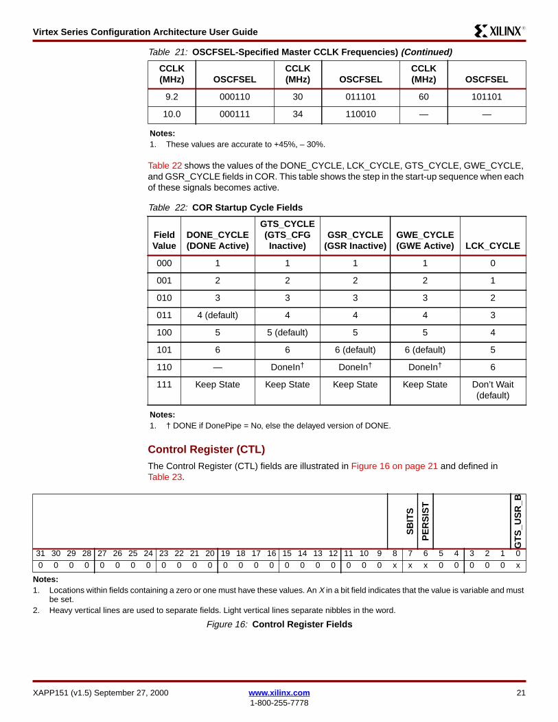
Virtex Series Configuration Architecture User GuideR13
Table 22 shows the values of the DONE_CYCLE LCK_CYCLE GTS_CYCLE GWE_CYCLEand GSR_CYCLE fields in COR This table shows the step in the start-up sequence when eachof these signals becomes active
Control Register (CTL)The Control Register (CTL) fields are illustrated in Figure 16 on page 21 and defined inTable 23
92 000110 30 011101 60 101101
100 000111 34 110010 mdash mdash
Notes1 These values are accurate to +45 ndash 30
Table 22 COR Startup Cycle Fields
FieldValue
DONE_CYCLE(DONE Active)
GTS_CYCLE(GTS_CFGInactive)
GSR_CYCLE(GSR Inactive)
GWE_CYCLE(GWE Active) LCK_CYCLE
000 1 1 1 1 0
001 2 2 2 2 1
010 3 3 3 3 2
011 4 (default) 4 4 4 3
100 5 5 (default) 5 5 4
101 6 6 6 (default) 6 (default) 5
110 mdash DoneIndagger DoneIndagger DoneIndagger 6
111 Keep State Keep State Keep State Keep State Donrsquot Wait(default)
Notes1 dagger DONE if DonePipe = No else the delayed version of DONE
Table 21 OSCFSEL-Specified Master CCLK Frequencies) (Continued)
CCLK(MHz) OSCFSEL
CCLK(MHz) OSCFSEL
CCLK(MHz) OSCFSEL
SB
ITS
PE
RS
IST
GT
S_U
SR
_B
31 30 29 28 27 26 25 24 23 22 21 20 19 18 17 16 15 14 13 12 11 10 9 8 7 6 5 4 3 2 1 00 0 0 0 0 0 0 0 0 0 0 0 0 0 0 0 0 0 0 0 0 0 0 x x x 0 0 0 0 0 x
Notes1 Locations within fields containing a zero or one must have these values An X in a bit field indicates that the value is variable and must
be set2 Heavy vertical lines are used to separate fields Light vertical lines separate nibbles in the word
Figure 16 Control Register Fields
XAPP151 (v15) September 27 2000 wwwxilinxcom 211-800-255-7778
Virtex Series Configuration Architecture User GuideR13
Cyclic Redundancy Check (CRC)A data input error checking mechanism is provided through the Cyclic Redundancy Check(CRC) register When data is written to any configuration register (except LOUT) a 16-bit CRCvalue is calculated using both the register data and the address This value is saved in the CRCregister At the end of any series of writes a pre-calculated CRC block-check value may bewritten to the CRC register If the resulting value is non-zero an error is indicated TheCRC_ERROR bit is accessible through the status register If a CRC error is detectedconfiguration logic is put in the ERROR mode The following section is an algorithm forcomputing CRC
CRC Algorithm Initialization bcc = 0skip_pad = truemore_words = true Check for write operation do
w = next_wordif (w[3127] == rsquo00101rsquo)
A Read OP Donrsquot use in CRCwc = w[100]if (wc == 0)
w = next_wordwc = w[190]
while (wc-- gt 0)
w = next_word
elsif (w[3127] == rsquo00110rsquo)
A Write OP Use in CRC addr = w[1613]if (addr Π0124569DB)
wc = w[100]if (wc == 0)
wc is in next word w = next_wordwc = w[190]
while (wc-- gt 0)
w = next_wordsw[350] = addr wordfor (i=0 ilt36 i++)
Table 23 Control Register Bits
NameBit
Indices Description
SBITS 87 Security level0 ReadWrite OK (default)1 Readback disabled23 Readback disabled Writing disabled except CRCregister
PERSIST 6 Configuration interface remains after configuration0 No (default)1 Yes
GTS_USR_B 0 Active-low global tristate IOs Turn off pull-ups ifGTS_CFG_B is also asserted
22 wwwxilinxcom XAPP151 (v15) September 27 20001-800-255-7778
Virtex Series Configuration Architecture User GuideR13
x16 = bcc[15] XOR sw[i]x15 = bcc[14] XOR x16x2 = bcc[1] XOR x16bcc[150] =
x15bcc[132]x2bcc[0]x16 Note the bit order crc[150] = bcc[015]
else
Pad word - ignore
while (more_words)
Frame Address Register (FAR)The Frame Address Register (FAR) holds the address of the current frame The address isdivided into three parts the block type the major address and the minor address The blocktype field indicates whether the CLB or block RAM address space is used The command in thecommand register is executed each time the FAR is loaded with a new value
The major address selects the CLB or RAM column the minor address selects the frame withinthe column The minor address is incremented each time a full data frame is read from orwritten to the frame data register If the last frame within the CLB column is selected when theincrement occurs the major address is incremented and the minor address is reset to zerootherwise the minor address is incremented However the block RAM major address is notincremented automatically
See Figure 18 for the definitions of valid values for the block type field The FAR field definitionsare shown in Figure 19
Figure 17 CRC Calculation Register
Note the Block RAM Major Address is not incremented automatically To address a differentBlock RAM Content column the FAR must be loaded with the new Major Address
Type CodesCLB 00RAM 01
Figure 18 Block Type Codes
x151_17_021100
15141312111098765432
1013
01234526272829303101
Address 32-bit Data Word
CRC Calculation Register
CRC Data Input Register
CRC Register [310]
DATA_IN
SHIFT
23
16-bit CRC13150
0000 0000 0000 0000133116
1313
XAPP151 (v15) September 27 2000 wwwxilinxcom 231-800-255-7778
Virtex Series Configuration Architecture User GuideR13
Frame Data Input Register (FDRI)The Frame Data Input Register (FDRI) is used to load configuration frame data into a Virtexdevice
The Frame Data Register (FDR) is a shift register into which data is loaded prior to transfer tothe configuration memory Configuration data is written to the Virtex device by loading thecommand register with the WCFG command and then loading the FDR with at least two framesof 32-bit words
The write operation is pipelined such that the first frame of data is written to the configurationmemory while the second frame is being shifted in The last frame (the pad frame) is alwaysdummy data which is not actually written to the configuration memory Each frame write mustinclude enough 32 bit data words to load the frame fully There is one pad word at the end ofeach frame which is required for the pipelining hardware
Frame Data Output Register (FDRO)The Frame Data Output Register (FDRO) is for reading configuration data or captured datafrom the Virtex device a process called readback Readback is performed by loading thecommand register with the RCFG command and then addressing the FDRO with a readcommand
Frame Length Register (FLR)Near the beginning of the configuration bitstream the Frame Length Register (FLR) is writtenwith the length of a frame as measured in 32-bit words This length count is used to providesequencing information for the configuration read and write operations Note that the FLR mustbe written before any FDR operation works It is not necessary to set the FLR more than onceIf the number of bits in a frame is not evenly divisible by 32 the length count of the frame mustbe rounded up to the next highest integer The values for the FLR for all the current Virtexseries devices are given in Table 24
BlockType
Major Address(Column Address)
Minor Address(Frame Address)
31 30 29 28 27 26 25 24 23 22 21 20 19 18 17 16 15 14 13 12 11 10 9 8 7 6 5 4 3 2 1 00 0 0 0 0 x x x x x x x x x x x x x x x x x x 0 0 0 0 0 0 0 0 0
Notes1 Locations within fields containing a zero or one must have these values An X in a bit field indicates that the value is variable and must
be set2 Heavy vertical lines are used to separate fields Light vertical lines separate nibbles in the word
Figure 19 Frame Address Fields (FAR)
Note The FLR contains a value that is one less than the number of words that are read fromor written to a given frame This is because the extra word needed for pipelining is not counted
Table 24 Frame Length Register Value
Device Row times Col Frame Length Words per Frame FLR Value
XCV50E 16 times 24 384 12 11
XCV100E 20 times 30 448 14 13
XCV150 24 times 36 512 16 15
XCV200E 28 times 42 576 18 17
XCV300E 32 times 48 672 21 20
24 wwwxilinxcom XAPP151 (v15) September 27 20001-800-255-7778
Virtex Series Configuration Architecture User GuideR13
Legacy Output Register (LOUT)The Legacy Output Register (LOUT) is used for daisy chaining the configuration bitstream toother Xilinx devices Data written to the LOUT is serialized and appears on the DOUT pin
Mask Register (MASK)The Mask Register (MASK) is a mask register for writes to the CTL register A 1 in bit N of themask allows that bit position to be written in the CTL register The default value of the mask isall 0s
Status Register (STAT)The Status Register (STAT) is loaded with current values of several control or status signalsThe register can be read via the re-configuration block or via JTAG The fields in the Statusregister are illustrated in Figure 20 The values of the signals given in Table 25 on page 26 canbe read from the status register
XCV400E 40 times 60 800 25 24
XCV405E 40 times 60 800 25 24
XCV600E 48 times 72 960 30 29
XCV800 56 times 84 1088 34 33
XCV812E 56 times 84 1088 34 33
XCV1000E 64 times 96 1248 39 38
XCV1600E 72 times 108 1376 43 42
XCV2000E 80 times 120 1536 48 47
XCV2600E 92 times 138 1728 54 53
XCV3200E 104 times 156 1952 61 60
Table 24 Frame Length Register Value (Continued)
Device Row times Col Frame Length Words per Frame FLR Value
DO
NE
INIT
MO
DE
GH
IGH
_B
GS
R_B
GW
E_B
GT
S_C
FG
IN_E
RR
OR
LOC
K
CR
C_E
RR
OR
31 30 29 28 27 26 25 24 23 22 21 20 19 18 17 16 15 14 13 12 11 10 9 8 7 6 5 4 3 2 1 00 0 0 0 0 0 0 0 0 0 0 0 0 0 0 0 0 x x x x x x x x x x x x x x x
Notes1 An X in a bit field indicates that the value is variable2 Heavy vertical lines are used to separate fields Light vertical lines separate nibbles in the word
Figure 20 Status Register Fields
XAPP151 (v15) September 27 2000 wwwxilinxcom 251-800-255-7778
Virtex Series Configuration Architecture User GuideR13
ConfigurationInterface
There are two configuration interfaces to the Virtex devices mdash the bit-serial Boundary Scaninterface and the 8-bit byte-serial SelectMAP interface Conceptually XCV50 configurationdata appears as in Figure 21
Frames and words within frames are written in the same order in both configuration interfacesstarting with Frame 0 word 0 (the left-most in the picture) followed by word 1 etc Bits withineach word are written from left to right (MSB first) in the bit-serial configuration interfaces
Within the SelectMAP interface data is written a byte at a time A sample word is shown inFigure 22 The top row indicates the device pin names The bottom row indicates the bit indiceswithin a configuration word Byte 0 loads first followed by byte 1 et cetera The MSB of eachbyte (ie bits 31 23 15 and 7) is loaded on pin D0 The LSB of each byte (ie bits 24 16 8and 0) is loaded on pin D7
PartialReconfigurationof CLBs
Partial reconfiguration can be performed with and without shutting down the device Ifcontention occurs it is advised to go through a shutdown sequence prior to loadingconfiguration frames When shutting down the DONE pin will go active and pull low If this is notdesireable the DONE pin can be prevented from going low by selecting the DONE_CYCLE toKeep State (111) Similarly to prevent GSR from becoming active and reseting the currentstate the GSR_CYCLE can be set to Keep State When not shutting down changes occurframe by frame but is completely done by the end of the Last Frame packet (see Example 1)
Table 25 Status Register Bits
Name Bit Indices Description
DONE 14 Input from DONE pin
INIT 13 Value of INIT
MODE 1210 Value of M2 M1 M0 mode pins
GHIGH_B 9 0 = GHIGH_B asserted
GSR_B 8 0 = all flip-flops are ResetSet
GWE_B 7 1 = flip-flops and block RAM are write disabled
GTS_CFG 6 0 = IOs are tri-stated
IN_ERROR 5 Legacy input error
LOCK 41 Output from DLL lock signals 1 = DLL is locked
CRC_ERROR 0 Indicates that a CRC error has occurred
Data Frame 0 (11 words) Pad Word
hellip
Data Frame n (11 words) Pad WordPad Frame (12 words)
Figure 21 XCV50 Frame Padding for Reads
Figure 22 SelectMAP Byte and Bit Ordering
x151_22_021100
D0 D1 D2 D3 D4 D5 D6 D7 D0 D1 D2 D3 D4 D5 D6 D7 D0 D1 D2 D3 D4 D5 D6 D7 D0 D1 D2 D3 D4 D5 D6 D7
Byte 0 Byte 1 Byte 2 Byte 313
26 wwwxilinxcom XAPP151 (v15) September 27 20001-800-255-7778
Virtex Series Configuration Architecture User GuideR13
The DONE pin will not change in this case Figure 23 illustrates a typical shutdownreconfiguration in the CLB address space and restart sequence
Examples Several examples of reading and evaluating configuration data are provided to illustrate thefollowing
Figure 23 Typical Shutdown Reconfiguration in the CLB Address Spaceand Restart Sequence
FFFF FFFF Dummy WordAA99 5566 Sync Word Does not realign an already synchronized SelectMap port3001 2001 COR0080 FF2F Shutdown bit set optionally set bit 29 DRIVE_DONE
Alternately COR may be read bit 15 set and written back3000 8001 CMD0000 0005 Start Shutdown3000 8001 CMD0000 0007 Reset CRC0000 00000000 0000 Clock shutdown sequence0000 00000000 00003000 8001 CMD0000 0008 Assert GHIGH3000 8001 CMD0000 0001 Write Configuration3000 2001 FAR0--- ---- Block Type CLB (00) MajorMinor Address3000 4--- FDRI + Word Count if count is lt1024 Otherwise use TypeII Header
Write FRAME DATAIf CLB Frames are not written to non-consecutive addresses repeat FAR word followedby new MajorMinor Address followed by FDRI + Word Count and then Frame Data
3000 0001 Write CRC---- ---- CRC3000 8001 CMD0000 0003 LFRM3000 4--- FDRI + Word Count
Write PAD FRAME
3001 2001 COR0080 3F2D Default COR Options
Alternately COR may be read bit 15 cleared and written back3000 8001 CMD0000 0005 Begin Startup3000 0001 Write CRC---- ---- CRC
0000 00000000 0000 4 Dummy Words0000 00000000 0000
Example 1 Read and Write Semaphores in an XCV100 at CLB R1 C1 Slice 0 on page 28Example 2 Reading the Complete Configuration from an XCV50 on page 33
XAPP151 (v15) September 27 2000 wwwxilinxcom 271-800-255-7778
Virtex Series Configuration Architecture User GuideR13
Example 1 Read and Write Semaphores in an XCV100 at CLB R1 C1Slice 0Semaphores are a useful communication mechanism documented in XAPP 153 ldquoStatus andControl Semaphore Registers using Partial Reconfigurationrdquo Figure 24 shows an abstractionof a microprocessor writing control information to an FPGA and reading status informationOne convention for implementing semaphores in Virtex devices is to use two bits of a 16-bitdual-port RAM as illustrated in Figure 25 This occupies one CLB slice with the F-LUTimplementing the control semaphore and the status semaphore implemented in the G-LUTAddress 15 of the G-LUT is used for on-chip writes to the semaphore and address 14 of the F-LUT is used for on-chip reads Conversely the off-chip microprocessor is reading the G-LUT[15] and writing F-LUT[14]
Example 3 Read the Slice 0 G-LUT from CLB R1 C1 from the Complete Configuration of anXCV50 on page 34Example 4 Read the Slice 1 F-LUT from CLB R19 C16 from an XCV100 on page 36Example 5 Read All Bits in Slice 0 G-LUTs from CLB C2 and XCV50 on page 39Example 6 Read Block SelectRAM index 387 of RAM R2 C0 from an XCV100E on page 41
Figure 24 Semaphore Abstraction
x151_ 23_021400
Status13
Control13
MicroProcessor FPGA13
Semaphores13
28 wwwxilinxcom XAPP151 (v15) September 27 20001-800-255-7778
Virtex Series Configuration Architecture User GuideR13
Using a Semaphore Abstraction dual-port RAM ensures that the LUT SelectRAMs are placedin the CLB in a predictable manner When writing data to one or more LUT SelectRAMs or flip-flops on the device all bits in the frame must have valid configuration information This isassured by altering valid configurations from bitstream files or from frames read from a properlyconfigured Virtex device The latter approach is used in this example
Figure 25 Semaphore ReadWrite Implementation
Frame 47
15
14
47 46
47 46
x151_ 24_021100
Select Map
Frame 46
DING
F
13
D2D3D4 5D6 7D0D1 D D
1
111
0
111
Chip Interface
G F
13
XAPP151 (v15) September 27 2000 wwwxilinxcom 291-800-255-7778
Virtex Series Configuration Architecture User GuideR13
Attributes for this design are summarized in Table 26
From the equations in Table 7 on page 11 the values shown in Table 27 can be calculated
From off-chip for reading the G-LUT[15] bit read one frame (MNA=47) For writing the F-LUT[14] bit we show how to read then write one frame (MNA=46) as opposed to modifyingdata from a bitstream file (both are valid methods) The frames on the XCV100 contain 13 32-bit words and one pad word Remember that fm_st_wd is calculated assuming the entireconfiguration has been read However only the pad frame and then frames 46 and 47 fromMajor Address 30 are being read The desired bit is in Frame 1 word 1 which is word 15
The commands for reading both frames (and the pad frame) are given in Figure 26
Table 26 Design Attributes for Example 1
Attribute
G-LUT [15] F-LUT [14]
Read Read Write
Chip_Rows 20
Chip_Cols 30
FL 14
CLB_Row 1
CLB_Col 1
Slice 0
FG 1 0
lut_bit 15 14
RW 1 1 0
Table 27 Semaphore Example Variables Equations and Values
Variable Equation
Value(s)
G-LUT[15] F-LUT[14]
Read Read Write
MJA 1 le 302 rArr 30 ndash 1 times 2 + 2 30
MNA lut_bit + 32ndash 0 times () 47 46
fm_bit_idx 3 + 18 times 1 ndash FG + RW times 32 52 53 21
fm_st_wd 14 times (8 + (30 ndash 1) times 48+ 4647) +RW times (14 +1)= 14 times (1400 + 4647) + 14 times RW= 19600 + 14 times 4647 + 14 times RW
20272 20258 20244
fm_wd floor (2032) 1 1 0
fm_wd_bit_idx 31 + 32 times 110 ndash 525321 11 10 10
30 wwwxilinxcom XAPP151 (v15) September 27 20001-800-255-7778
Virtex Series Configuration Architecture User GuideR13
The 42 words read are shown in Figure 27 F-LUT[14] is in the second frame (frame=1word=1) at bit 10 The value read is a 1 but because the LUT bits are inverted the logic valueis zero G-LUT[15] is in word one of the third data frame (frame=2 word=1) at bit 11The valueread is a 1 which is a logic zero
InstructionData
Hex 31 30 29 28 27 26 25 24 23 22 21 20 19 18 17 16 15 14 13 12 11 10 9 8 7 6 5 4 3 2 1 0
Sync Word AA99 5566 1 0 1 0 1 0 1 0 1 0 0 1 1 0 0 1 0 1 0 1 0 1 0 1 0 1 1 0 0 1 1 0
Write next (1) word to FAR 3000 2001 0 0 1 1 0 0 0 0 0 0 0 0 0 0 0 0 0 0 1 0 0 0 0 0 0 0 0 0 0 0 0 1
CLB MJA=30 MNA=46 003C 5800 0 0 0 0 0 0 0 0 0 0 1 1 1 1 0 0 0 1 0 1 1 1 0 0 0 0 0 0 0 0 0 0
Write next word to CMD 3000 8001 0 0 1 1 0 0 0 0 0 0 0 0 0 0 0 0 1 0 0 0 0 0 0 0 0 0 0 0 0 0 0 1
Register value for RCFG 0000 0004 0 0 0 0 0 0 0 0 0 0 0 0 0 0 0 0 0 0 0 0 0 0 0 0 0 0 0 0 0 1 0 0
Read from FDRO 2800 602A 0 0 1 0 1 0 0 0 0 0 0 0 0 0 0 0 0 1 1 0 0 0 0 0 0 0 1 0 1 0 1 0
Flush pipe 0000 0000 0 0 0 0 0 0 0 0 0 0 0 0 0 0 0 0 0 0 0 0 0 0 0 0 0 0 0 0 0 0 0 0
(read 42 words)
Notes1 Binary data is grouped in two ways for ease of interpretation Thin vertical lines separate nibble boundaries Heavy vertical lines
separate field boundaries
Figure 26 Commands to Read Two Data Frames
XAPP151 (v15) September 27 2000 wwwxilinxcom 311-800-255-7778
Virtex Series Configuration Architecture User GuideR13
To write to the F-LUT semaphore start with the second data frame (frame=1) that was justread Words 1 - 13 of that frame will become words 0 - 12 of the frame to be written Word 13of this new frame is a pad word and can have any value (typically 0 is chosen) In this newframe set bit 11 of word 0 (zero) to the desired value of the semaphore A pad frame mustfollow the data frame The commands from Figure 28 write these two frames into the device atthe proper location
Frame Word 31 30 29 28 27 26 25 24 23 22 21 20 19 18 17 16 15 14 13 12 11 10 9 8 7 6 5 4 3 2 1 0
0
0 1 1 1 1 1 1 1 1 1 1 1 1 1 1 1 1 1 1 1 1 1 1 1 1 1 1 1 1 1 1 1 1
1 1 1 1 1 1 1 1 1 1 1 1 1 1 1 1 1 1 1 1 1 1 1 1 1 1 1 1 1 1 1 1 1
2 1 1 1 1 1 1 1 1 1 1 1 1 1 1 1 1 1 1 1 1 1 1 1 1 1 1 1 1 1 1 1 1
3 1 1 1 1 1 1 1 1 1 1 1 1 1 1 1 1 1 1 1 1 1 1 1 1 1 1 1 1 1 1 1 1
4 1 1 1 1 1 1 1 1 1 1 1 1 1 1 1 1 1 1 1 1 1 1 1 1 1 1 1 1 1 1 1 1
5 1 1 1 1 1 1 1 1 1 1 1 1 1 1 1 1 1 1 1 1 1 1 1 1 1 1 1 1 1 1 1 1
6 1 1 1 1 1 1 1 1 1 1 1 1 1 1 1 1 1 1 1 1 1 1 1 1 1 1 1 1 1 1 1 1
7 1 1 1 1 1 1 1 1 1 1 1 1 1 1 1 1 1 1 1 1 1 1 1 1 1 1 1 1 1 1 1 1
8 1 1 1 1 1 1 1 1 1 1 1 1 1 1 1 1 1 1 1 1 1 1 1 1 1 1 1 1 1 1 1 1
9 1 1 1 1 1 1 1 1 1 1 1 1 1 1 1 1 1 1 1 1 1 1 1 1 1 1 1 1 1 1 1 1
10 1 1 1 1 1 1 1 1 1 1 1 1 1 1 1 1 1 1 1 1 1 1 1 1 1 1 1 1 1 1 1 1
11 1 1 1 1 1 1 1 1 1 1 1 1 1 1 1 1 1 1 1 1 1 1 1 1 1 1 1 1 1 1 1 1
12 1 1 1 1 1 1 1 1 1 1 1 1 1 1 1 1 1 1 1 1 1 1 1 1 1 1 1 1 1 1 1 1
13 1 1 1 1 1 1 1 1 1 1 1 1 1 1 1 1 1 1 1 1 1 1 1 1 1 1 1 1 1 1 1 1
1
0 0 0 0 0 0 0 0 0 0 0 0 0 0 0 0 0 0 0 0 0 0 0 0 0 0 0 0 0 0 0 0 0
1 1 0 0 0 0 0 0 0 0 0 0 0 1 0 0 0 0 1 1 0 1 1 0 0 0 0 0 0 0 0 0 0 F[14]
2 1 1 1 1 1 0 1 1 0 0 0 0 1 1 1 1 0 0 1 1 1 1 1 0 1 1 0 0 0 0 0 0
3 0 0 0 0 1 1 1 1 1 0 1 1 0 0 0 0 0 0 0 0 0 0 1 1 1 1 1 0 1 1 0 0
4 0 0 0 0 0 0 0 0 1 1 1 1 0 0 0 0 0 0 0 0 0 0 0 0 0 0 1 1 1 1 1 0
5 1 1 0 0 1 1 0 0 0 0 0 0 1 1 0 0 1 0 1 1 0 0 0 0 0 0 0 0 0 0 1 1
6 1 1 1 0 1 1 0 0 0 0 0 0 1 1 1 0 1 1 1 0 1 0 1 1 0 0 0 0 0 0 0 0
7 0 0 1 1 1 1 1 0 1 1 0 0 0 0 1 1 0 0 0 0 1 1 1 1 1 0 1 1 0 0 0 0
8 0 0 0 0 0 0 1 1 1 1 1 0 0 0 0 0 0 0 0 0 0 0 0 0 1 1 1 1 1 0 1 1
9 0 0 0 0 0 0 0 0 0 0 1 1 0 0 0 0 1 1 0 0 0 0 0 0 0 0 0 0 1 1 1 1
10 1 0 1 1 0 0 0 0 0 0 0 0 1 0 1 1 1 1 1 0 1 1 0 0 0 0 0 0 0 0 0 0
11 1 1 1 1 1 0 1 1 0 0 0 0 1 1 1 1 0 0 1 1 1 1 1 0 1 1 0 0 0 0 0 0
12 0 0 0 0 1 1 0 1 1 0 1 1 0 0 0 0 0 0 0 0 0 0 1 1 1 1 1 0 0 0 0 0
13 0 0 0 0 0 0 1 1 0 1 0 1 0 0 0 0 0 0 0 0 0 0 0 0 0 0 0 0 0 0 0 0
2
0 0 0 0 0 0 0 0 0 0 0 0 0 0 0 0 0 0 0 0 0 0 0 0 0 0 0 0 0 0 0 0 0
1 1 0 1 0 0 0 0 0 0 0 0 1 1 0 1 0 1 1 1 0 1 1 0 0 0 0 0 0 0 0 0 0 G[15]
2 1 1 1 1 1 1 1 1 0 0 0 0 1 1 1 1 0 0 1 1 1 1 1 1 1 1 0 0 0 0 0 0
3 0 0 0 0 1 1 1 1 1 1 1 1 0 0 0 0 0 0 0 0 0 0 1 0 1 1 1 1 1 1 0 0
4 0 0 0 0 0 0 0 0 1 1 1 1 0 0 0 0 0 0 0 0 0 0 0 0 0 0 1 1 1 1 1 1
5 1 1 0 0 0 0 0 0 0 0 0 0 1 1 0 0 1 1 1 1 0 0 1 0 0 0 0 0 0 0 1 1
6 1 1 1 1 1 1 0 0 0 0 0 0 1 1 1 1 1 1 1 1 1 1 1 1 0 0 0 0 0 0 0 0
7 0 0 1 1 1 1 1 1 1 1 0 0 0 0 1 1 0 0 0 0 1 1 1 1 1 1 1 1 0 0 0 0
8 0 0 0 0 0 0 1 1 1 1 1 1 0 0 0 0 0 0 0 0 0 0 0 0 1 1 1 1 1 1 1 1
9 0 0 0 0 0 0 0 0 0 0 1 1 0 0 0 0 1 1 0 0 0 0 0 0 0 0 0 0 1 1 1 1
10 1 1 1 1 0 0 0 0 0 0 0 0 1 1 1 1 1 1 1 1 1 1 0 0 0 0 0 0 0 0 0 0
11 1 1 1 1 1 1 1 1 0 0 0 0 1 1 1 1 0 0 1 1 1 1 1 1 1 1 0 0 0 0 0 0
12 0 0 0 0 1 1 0 1 1 1 1 1 0 0 0 0 0 0 0 0 0 0 1 1 1 1 1 0 1 0 0 0
13 0 0 0 0 0 1 1 0 0 1 1 1 0 0 0 0 0 0 0 0 0 0 0 0 0 0 0 0 0 0 0 0
Figure 27 Three Frames Containing the Semaphores
32 wwwxilinxcom XAPP151 (v15) September 27 20001-800-255-7778
Virtex Series Configuration Architecture User GuideR13
Example 2 Reading the Complete Configuration from an XCV50Steps
1 If flip-flop values are needed clock the on-chip signal CAPTURE to capture flip-flopvalues See the Xilinx Libraries Guide for use of the CAPTURE_VIRTEX cell
2 Write the starting frame address (CLB MJA=0 MNA=0) into the FAR
3 Write the RCFG command to the CMD register
4 Address the FDRO register with a READ operation and word count equal to the number of32-bit words in the CLB frames plus one pad frame
5 Read the data following the timing diagrams in the SelectMAP interface section
6 Write the address for RAM block 0 to the FAR
7 Address the FDRO register with a read operation and word count equal to the number of32-bit words in the RAM block plus one pad frame
8 Read the data
9 Write the address for RAM block 1 to the FAR
10 Address the FDRO register with a read operation and word count equal to the number of32-bit words in the RAM block plus one pad frame
11 Read the data
When using SelectMAP mode to read data words from the Virtex device de-assert CS de-assert WRITE assert CS then clock the data out When using JTAG load the JTAG IR
InstructionData
Hex 31 30 29 28 27 26 25 24 23 22 21 20 19 18 17 16 15 14 13 12 11 10 9 8 7 6 5 4 3 2 1 0
Sync Word AA995566
1 0 1 0 1 0 1 0 1 0 0 1 1 0 0 1 0 1 0 1 0 1 0 1 0 1 1 0 0 1 1 0
Write next (1) word to FAR 30002001
0 0 1 1 0 0 0 0 0 0 0 0 0 0 0 0 0 0 1 0 0 0 0 0 0 0 0 0 0 0 0 1
MJA=30 MNA=46 003C5C00
0 0 0 0 0 0 0 0 0 0 1 1 1 1 0 0 0 1 0 1 1 1 0 0 0 0 0 0 0 0 0 0
Write next word to CMD 30008001
0 0 1 1 0 0 0 0 0 0 0 0 0 0 0 0 1 0 0 0 0 0 0 0 0 0 0 0 0 0 0 1
Register value for WCFG 00000001
0 0 0 0 0 0 0 0 0 0 0 0 0 0 0 0 0 0 0 0 0 0 0 0 0 0 0 0 0 0 0 1
Write 28 words to FDRI 3000401C
0 0 1 1 0 0 0 0 0 0 0 0 0 0 0 0 0 1 0 0 0 0 0 0 0 0 0 1 1 1 0 0
Data Word 0 A01AEC00
1 0 1 0 0 0 0 0 0 0 0 1 1 0 1 0 1 1 1 0 1 1 0 0 0 0 0 0 0 0 0 0
Data Word 1 FF0F3FC0
1 1 1 1 1 1 1 1 0 0 0 0 1 1 1 1 0 0 1 1 1 1 1 1 1 1 0 0 0 0 0 0
Data Word 2 0FF002FC
0 0 0 0 1 1 1 1 1 1 1 1 0 0 0 0 0 0 0 0 0 0 1 0 1 1 1 1 1 1 0 0
hellip hellip hellip
Data Word 27 00000000
0 0 0 0 0 0 0 0 0 0 0 0 0 0 0 0 0 0 0 0 0 0 0 0 0 0 0 0 0 0 0 0
Notes1 Binary data is grouped in two ways for ease of interpretation Thin vertical lines separate nibble boundaries Heavy
vertical lines separate field boundaries
Figure 28 Commands to Write a Semaphore Value
XAPP151 (v15) September 27 2000 wwwxilinxcom 331-800-255-7778
Virtex Series Configuration Architecture User GuideR13
(instruction register) with the CFG_OUT instruction Then go to the SDR (Shift-DR) state andshift the data out (See Figure 29)
Example 3 Read the Slice 0 G-LUT from CLB R1 C1 from the CompleteConfiguration of an XCV50The commands for reading the bitstream from the Virtex device are given in Example 1 Readand Write Semaphores in an XCV100 at CLB R1 C1 Slice 0 on page 28 Using an XCV50device the independent attributes are show in Table 28
InstructionData
Hex 31 30 29 28 27 26 25 24 23 22 21 20 19 18 17 16 15 14 13 12 11 10 9 8 7 6 5 4 3 2 1 0
Sync Word AA99 5566 1 0 1 0 1 0 1 0 1 0 0 1 1 0 0 1 0 1 0 1 0 1 0 1 0 1 1 0 0 1 1 0
Write next word to FAR 3000 2001 0 0 1 1 0 0 0 0 0 0 0 0 0 0 0 0 0 0 1 0 0 0 0 0 0 0 0 0 0 0 0 1
CLB MJA=0 MNA=0 0000 0000 0 0 0 0 0 0 0 0 0 0 0 0 0 0 0 0 0 0 0 0 0 0 0 0 0 0 0 0 0 0 0 0
Write next word to CMDregister
3000 8001 0 0 1 1 0 0 0 0 0 0 0 0 0 0 0 0 1 0 0 0 0 0 0 0 0 0 0 0 0 0 0 1
Register value for RCFG 0000 0004 0 0 0 0 0 0 0 0 0 0 0 0 0 0 0 0 0 0 0 0 0 0 0 0 0 0 0 0 0 1 0 0
Read from FDRO register 2800 6000 0 0 1 0 1 0 0 0 0 0 0 0 0 0 0 0 0 1 1 0 0 0 0 0 0 0 0 0 0 0 0 0
15876 words 4800 3E04 0 1 0 0 1 0 0 0 0 0 0 0 0 0 0 0 0 0 1 1 1 1 1 0 0 0 0 0 0 1 0 0
Flush pipe 0000 0000 0 0 0 0 0 0 0 0 0 0 0 0 0 0 0 0 0 0 0 0 0 0 0 0 0 0 0 0 0 0 0 0
(Read 15876 words)Write to FAR register 3000 2001 0 0 1 1 0 0 0 0 0 0 0 0 0 0 0 0 0 0 1 0 0 0 0 0 0 0 0 0 0 0 0 1
RAM MJA=0 MNA=0 0200 0000 0 0 0 0 0 0 1 0 0 0 0 0 0 0 0 0 0 0 0 0 0 0 0 0 0 0 0 0 0 0 0 0
Read 780 words fromFDRO reg
2800 630C 0 0 1 0 1 0 0 0 0 0 0 0 0 0 0 0 0 1 1 0 0 0 1 1 0 0 0 0 1 1 0 0
Flush pipe 0000 0000 0 0 0 0 0 0 0 0 0 0 0 0 0 0 0 0 0 0 0 0 0 0 0 0 0 0 0 0 0 0 0 0
(Read 780 words)Write to FAR register 3000 2001 0 0 1 1 0 0 0 0 0 0 0 0 0 0 0 0 0 0 1 0 0 0 0 0 0 0 0 0 0 0 0 1
RAM MJA=1 MNA=0 0202 0000 0 0 0 0 0 0 1 0 0 0 0 0 0 0 1 0 0 0 0 0 0 0 0 0 0 0 0 0 0 0 0 0
Read 780 words fromFDRO reg
2800 630C 0 0 1 0 1 0 0 0 0 0 0 0 0 0 0 0 0 1 1 0 0 0 1 1 0 0 0 0 1 1 0 0
Flush pipe 0000 0000 0 0 0 0 0 0 0 0 0 0 0 0 0 0 0 0 0 0 0 0 0 0 0 0 0 0 0 0 0 0 0 0
(Read 780 words)
Figure 29 Example 2 - Read Complete Configuration for XCV50
Table 28 XCV50 Independent Attributes
Independent Attributes Values
Chip_Rows 16
Chip_Cols 24
FL 12
CLB_Row 1
CLB_Col 1
FG 1
Slice 0
RW 1
34 wwwxilinxcom XAPP151 (v15) September 27 20001-800-255-7778
Virtex Series Configuration Architecture User GuideR13
From the equations given earlier in Table 7 calculating the range of values for fm_st_wdindicates that the word 13740 of the configuration is the starting word of the 12-word (FL=12)frame containing bit 0 of the G-LUT in Slice 0 of CLB R1C1 (Table 29)
The configuration bits for the given frame are as follows G-LUT[0] is in fm_wd=0 at bit 11
All 16 LUT SelectRAM bits are in the following words at the same bit index 11
Table 29 Variables Equations and Values for Slice 0 G-LUT
Variables Equations Values
MJA 1 le 242 rArr 24 ndash 1times 2 + 2 24
MNA 0 times (hellip) + lut_bit + 32 0 321 332 343 35
4 365 376 387 39
8 409 41
10 4211 43
12 4413 4514 4615 47
fm_bit_idx 3 + 18 times 1 ndash1 + RW times 32 52
fm_st_wd 12 times (8+ (24 ndash1) times 48 + [3247]) +1 x 12= 12 times (1112 + [3247]) +12= 13356 + 12 times 3247]
1374013920
fm_wd floor(5232) 1
fm_wd_bit_idx 31 + 32 ndash 52 11
BitstreamWord
Frame 32-bit Word FrameWord31 30 29 28 27 26 25 24 23 22 21 20 19 18 17 16 15 14 13 12 11 10 9 8 7 6 5 4 3 2 1 0
13740 0 0 0 0 0 0 0 0 0 0 0 0 0 0 0 0 0 0 0 0 0 0 0 0 0 0 0 0 0 0 0 0 013741 0 0 1 0 1 0 0 0 0 0 0 0 0 1 0 1 0 1 0 0 1 1 1 0 0 0 0 0 0 0 0 0 113742 1 0 1 1 0 0 1 1 0 0 0 0 0 0 0 0 0 0 1 0 1 1 0 0 1 1 0 0 0 0 0 0 213743 0 0 0 0 1 0 1 1 0 0 1 1 0 0 0 0 0 0 0 0 0 0 1 0 1 1 0 0 1 1 0 0 313744 0 0 0 0 0 0 0 0 1 0 1 1 0 0 1 1 0 0 0 0 0 0 0 0 0 0 1 0 1 1 0 0 413745 1 1 0 0 0 0 0 0 0 0 0 0 1 0 1 1 0 0 1 1 0 0 0 0 0 0 0 0 0 0 1 0 513746 1 1 0 0 1 1 0 0 0 0 0 0 0 0 0 0 1 0 1 1 0 0 1 1 0 0 0 0 0 0 0 0 613747 0 0 1 0 1 1 0 0 1 1 0 0 0 0 0 0 0 0 0 0 1 0 1 1 0 0 1 1 0 0 0 0 713748 0 0 0 0 0 0 1 0 1 1 0 0 1 1 0 0 0 0 0 0 0 0 0 0 1 0 1 1 0 0 1 1 813749 0 0 0 0 0 0 0 0 0 0 1 0 1 1 0 0 1 1 0 0 0 0 0 0 0 0 0 0 1 0 1 1 913750 0 0 1 1 0 0 0 0 0 0 0 0 0 0 1 0 1 1 0 0 1 0 1 0 0 0 0 0 0 0 0 0 1013751 0 1 0 1 0 0 0 0 0 0 0 0 0 0 0 0 0 0 0 0 0 0 0 0 0 0 0 0 0 0 0 0 11
Figure 30 Configuration Bits for Slice 0 CLB R1C1 G-LUT [0]
XAPP151 (v15) September 27 2000 wwwxilinxcom 351-800-255-7778
Virtex Series Configuration Architecture User GuideR13
The 16 bits are LUT[150]=0111111111111111 The LUT SelectRAM bits are inverted from theirlogic values The ldquologicalrdquo contents are LUT[150]=1000000000000000 Thus this G-LUTimplements a 4-input AND function
Example 4 Read the Slice 1 F-LUT from CLB R19 C16 from an XCV100Commands for reading the bitstream from the Virtex device are given in Figure 32 Use thefollowing independent attributes to find the given F-LUT
From the equations in Table 7 on page 11 calculating fm_st_wd indicates the starting wordwith respect to a configuration that starts at MJA=0 MNA=0 Because the frames we are
BitstreamWord
Frame 32-bit Word
LUT Bit31 30 29 28 27 26 25 24 23 22 21 20 19 18 17 16 15 14 13 12 11 10 9 8 7 6 5 4 3 2 1 0
13741 0 0 1 0 1 0 0 0 0 0 0 0 0 1 0 1 0 1 0 0 1 1 1 0 0 0 0 0 0 0 0 0 0
13753 1 0 1 0 0 0 0 0 0 0 0 0 0 0 0 1 0 0 0 1 1 1 0 0 0 0 0 0 0 0 0 0 1
13765 1 0 1 0 1 0 0 0 0 0 0 0 1 0 0 0 0 0 0 1 1 1 1 0 0 0 0 0 0 0 0 0 2
13777 0 0 0 0 1 0 0 0 0 0 0 1 1 1 0 1 1 0 1 0 1 1 0 0 0 0 0 0 0 0 0 0 3
13789 0 1 0 0 0 0 0 0 0 0 0 0 0 1 0 1 1 1 1 1 1 1 1 0 0 0 0 0 0 0 0 0 4
13801 1 0 1 0 1 0 0 0 0 0 0 1 0 0 0 1 1 0 0 1 1 1 0 0 0 0 0 0 0 0 0 0 5
13813 0 0 0 1 0 0 0 0 0 0 0 0 0 0 0 0 1 0 0 1 1 1 0 0 0 0 0 0 0 0 0 0 6
13825 0 1 1 0 1 0 0 0 0 0 0 1 0 1 0 0 1 1 0 0 1 1 0 0 0 0 0 0 0 0 0 0 7
13837 1 0 1 1 1 0 0 0 0 0 0 1 0 1 0 1 1 0 0 0 1 1 0 0 0 0 0 0 0 0 0 0 8
13849 1 0 0 0 0 0 0 0 0 0 0 0 0 0 0 0 1 1 1 0 1 1 0 0 0 0 0 0 0 0 0 0 9
13861 1 0 0 0 0 0 0 0 0 0 0 1 0 0 0 0 1 1 1 1 1 1 1 0 0 0 0 0 0 0 0 0 10
13873 1 0 0 0 0 0 0 1 0 0 0 0 0 1 0 0 0 1 1 0 1 1 0 0 0 1 0 0 0 0 0 0 11
13885 1 0 0 0 0 0 0 0 0 0 0 0 0 1 0 1 0 0 1 0 1 1 0 0 0 0 0 0 0 0 0 0 12
13897 0 0 0 0 1 0 0 0 0 0 0 0 0 1 0 0 0 0 0 0 1 1 0 0 0 0 0 0 0 0 0 0 13
13909 1 0 0 0 0 0 0 0 0 0 0 0 1 1 0 1 0 1 1 0 1 1 0 0 0 0 0 0 0 0 0 0 14
13921 1 0 1 0 0 0 0 0 0 0 0 1 1 1 0 1 1 1 1 1 0 1 0 0 0 0 0 0 0 0 0 0 15
Figure 31 Location of all 16 LUT SelectRAM Bits
Table 30 Virtex Bitstream Command Attributes
Independent Attributes Values
Chip_Rows 20
Chip_Cols 30
FL 14
CLB_Row 19
CLB_Col 16
FG 0
Slice 1
RW 1
36 wwwxilinxcom XAPP151 (v15) September 27 20001-800-255-7778
Virtex Series Configuration Architecture User GuideR13
interested in start at MJA=1 MNA=0 which is fm_st_wd = 126 so the first 126 words are notneeded (0ndash125) Therefore to find the given Slice 1 F-LUT see Table 31
Sixteen frames need to be read one for each bit in the LUT SelectRAM The bits in LUTSelectRAMs in Slice 1 occur in the opposite order that they do for Slice 0 LUT SelectRAMs
Frames are read sequentially with ascending addresses If read in LUT bit order LUT[0]LUT[1] hellip LUT[15] These are stored in descending addresses which require 16 separateread operations each reading one data frame and one pad frame However if read inascending address order LUT[15] LUT[14] hellip LUT[0] all 16 data frames are read with asingle read operation This requires only one pad frame for all 16 frames Thus it takes lesstime to read ascending frames starting at MJA=1 MNA=0 and finishing with frame MJA=1MNA=15 The frames in the XCV100 contain 14 32-bit words and a single pad wordCommands for reading only the F-LUT data are given in Figure 32
Table 31 Variables Equations and Values for Slice 1 F-LUT
Variables Equations Values
MJA 16 gt 302 rArr 2times16 ndash 30 ndash1 1
MNA lut_bit + 32 ndash Slice times (2 times lut_bit +17)= [015] + 32 ndash (2 times [015] + 17)= 15 ndash [015]
0 151 142 133 12
4 115 106 97 8
8 79 6
10 511 4
12 313 214 115 0
fm_bit_idx 3 + 18 times 19 ndash 0+ 32 377
fm_st_wd 14 times (8 + (1ndash 1) times 48 + [150]) +1 times 14= 14 times (8 + [150]) +14= 126 + 14 times [150]
= 336126
fm_wd floor(37732) 11
fm_wd_bit_idx 31 + 32 times 11 ndash 377 6
XAPP151 (v15) September 27 2000 wwwxilinxcom 371-800-255-7778
Virtex Series Configuration Architecture User GuideR13
The 377th bit of each frame is the bit in the F-LUT This LUT SelectRAM bit is in the framersquosword index 11 bit index 6
The configuration bits for the given frame in Figure 33 are as follows LUT Bit 15 is in MJA=1MNA=0 fm_wd=11 at bit 6
LUT bit 0 is in MJA=1 MNA=15 fm_wd=11 at bit 6
InstructionData
Hex 31 30 29 28 27 26 25 24 23 22 21 20 19 18 17 16 15 14 13 12 11 10 9 8 7 6 5 4 3 2 1 0
Sync Word AA99 5566 1 0 1 0 1 0 1 0 1 0 0 1 1 0 0 1 0 1 0 1 0 1 0 1 0 1 1 0 0 1 1 0
Write next (1) word to FAR 3000 2001 0 0 1 1 0 0 0 0 0 0 0 0 0 0 0 0 0 0 1 0 0 0 0 0 0 0 0 0 0 0 0 1
CLB MJA = 1 MNA = 0 0002 0000 0 0 0 0 0 0 0 0 0 0 0 0 0 0 1 0 0 0 0 0 0 0 0 0 0 0 0 0 0 0 0 0
Write next word to CMD 3000 8001 0 0 1 1 0 0 0 0 0 0 0 0 0 0 0 0 1 0 0 0 0 0 0 0 0 0 0 0 0 0 0 1
Register value for RCFG 0000 0004 0 0 0 0 0 0 0 0 0 0 0 0 0 0 0 0 0 0 0 0 0 0 0 0 0 0 0 0 0 1 0 0
Read from FDRO 2800 60EE 0 0 1 0 1 0 0 0 0 0 0 0 0 0 0 0 0 1 1 0 0 0 0 0 1 1 1 0 1 1 1 0
Flush pipe 0000 0000 0 0 0 0 0 0 0 0 0 0 0 0 0 0 0 0 0 0 0 0 0 0 0 0 0 0 0 0 0 0 0 0
(Read 238 words)
Figure 32 Commands to read Slice 1 F-LUT
Frame WordFrame 32-bit Word
31 30 29 28 27 26 25 24 23 22 21 20 19 18 17 16 15 14 13 12 11 10 9 8 7 6 5 4 3 2 1 0
0 0 0 0 0 0 0 0 0 0 0 0 0 0 0 0 0 0 0 0 0 0 0 0 0 0 0 0 0 0 0 0 0
1 1 1 0 0 0 0 0 0 0 0 0 0 0 1 0 1 1 1 1 1 1 1 0 0 0 0 0 0 0 0 0 0
2 1 1 1 1 1 1 1 1 0 0 0 0 0 0 0 0 0 0 1 1 1 1 1 1 1 1 0 0 0 0 0 0
3 0 0 0 0 1 1 1 1 1 1 1 1 0 0 0 0 0 0 0 0 0 0 1 1 1 1 1 1 1 1 0 0
4 0 0 0 0 0 0 0 0 1 1 1 1 1 1 1 1 0 0 0 0 0 0 0 0 0 0 1 1 1 1 1 1
5 1 1 0 0 0 0 0 0 0 0 0 0 1 1 1 1 1 1 1 1 0 0 0 0 0 0 0 0 0 0 1 1
6 1 1 1 1 1 1 0 0 0 0 0 0 0 0 0 0 1 1 1 1 1 1 1 1 0 0 0 0 0 0 0 0
7 0 0 1 1 1 1 1 1 1 1 0 0 0 0 0 0 0 0 0 0 1 1 1 1 1 1 1 1 0 0 0 0
8 0 0 0 0 0 0 1 1 1 1 1 1 1 1 0 0 0 0 0 0 0 0 0 0 1 1 1 1 1 1 1 1
9 0 0 0 0 0 0 0 0 0 0 1 1 1 1 1 1 1 1 0 0 0 0 0 0 0 0 0 0 1 1 1 1
10 1 1 1 1 0 0 0 0 0 0 0 0 0 0 1 1 1 1 1 1 1 1 0 0 0 0 0 0 0 0 0 0
11 1 1 1 1 1 1 1 1 0 0 0 0 0 0 0 0 0 0 1 1 1 1 1 1 1 0 0 0 0 0 0 0
12 0 0 0 0 1 1 1 1 1 1 1 1 0 0 0 0 0 0 0 0 0 0 1 1 1 1 1 1 0 0 0 0
13 0 0 0 0 0 0 0 0 0 1 1 1 0 0 0 0 0 0 0 0 0 0 1 1 1 1 1 1 0 0 0 0
Figure 33 Frame Containing F-LUT[15]
Bit streamWord
Frame 32-bit WordFmWd31 30 29 28 27 26 25 24 23 22 21 20 19 18 17 16 15 14 13 12 11 10 9 8 7 6 5 4 3 2 1 0
336 0 0 0 0 0 0 0 0 0 0 0 0 0 0 0 0 0 0 0 0 0 0 0 0 0 0 0 0 0 0 0 0 0337 0 1 0 0 1 0 0 0 0 0 0 1 0 1 0 0 1 1 0 0 1 1 0 0 0 0 0 0 0 0 0 0 1338 1 0 1 1 0 0 1 1 0 0 0 0 0 0 0 0 0 0 1 0 1 1 0 0 1 1 0 0 0 0 0 0 2339 0 0 0 0 1 0 1 1 0 0 1 1 0 0 0 0 0 0 0 0 0 0 1 0 1 1 0 0 1 1 0 0 3340 0 0 0 0 0 0 0 0 1 0 1 1 0 0 1 1 0 0 0 0 0 0 0 0 0 0 1 0 1 1 0 0 4341 1 1 0 0 0 0 0 0 0 0 0 0 1 0 1 1 0 0 1 1 0 0 0 0 0 0 0 0 0 0 1 0 5342 1 1 0 0 1 1 0 0 0 0 0 0 0 0 0 0 1 0 1 1 0 0 1 1 0 0 0 0 0 0 0 0 6343 0 0 1 0 1 1 0 0 1 1 0 0 0 0 0 0 0 0 0 0 1 0 1 1 0 0 1 1 0 0 0 0 7
Figure 34 Frame Containing F-LUT [0]
38 wwwxilinxcom XAPP151 (v15) September 27 20001-800-255-7778
Virtex Series Configuration Architecture User GuideR13
For the sake of brevity here are the sixteen 11th words in the order they appear in thebitstream
The bits are LUT[150]=0111111111111111 The LUT SelectRAM bits are inverted from thelogic sense The logical contents are LUT[150]=1000000000000000 Thus this F-LUTimplements a 4-input AND gate
Example 5 Read All Bits in Slice 0 G-LUTs from CLB C2 and XCV50Given the following attributes the necessary values to find the G-LUT data can be computed
344 0 0 0 0 0 0 1 0 1 1 0 0 1 1 0 0 0 0 0 0 0 0 0 0 1 0 1 1 0 0 1 1 8345 0 0 0 0 0 0 0 0 0 0 1 0 1 1 0 0 1 1 0 0 0 0 0 0 0 0 0 0 1 0 1 1 9346 0 0 1 1 0 0 0 0 0 0 0 0 0 0 1 0 1 1 0 0 1 1 0 0 0 0 0 0 0 0 0 0 10347 1 1 1 1 1 0 1 1 0 0 0 0 0 0 0 0 0 0 1 0 1 1 1 0 1 1 0 1 0 0 0 0 11348 0 0 0 0 1 1 1 0 1 0 1 1 0 0 0 0 0 0 0 0 0 0 1 1 1 1 0 1 0 0 0 0 12349 0 0 0 0 0 1 0 0 0 0 1 0 0 0 0 0 0 0 0 0 0 0 0 0 0 0 0 0 0 0 0 0 13
Bit streamWord
Frame 32-bit WordFmWd31 30 29 28 27 26 25 24 23 22 21 20 19 18 17 16 15 14 13 12 11 10 9 8 7 6 5 4 3 2 1 0
Figure 34 Frame Containing F-LUT [0]
BitstreamWord
Frame 32-bit WordLUT Bit31 30 29 28 27 26 25 24 23 22 21 20 19 18 17 16 15 14 13 12 11 10 9 8 7 6 5 4 3 2 1 0
137 1 1 1 1 1 1 1 1 0 0 0 0 0 0 0 0 0 0 1 1 1 1 1 1 1 0 0 0 0 0 0 0 15151 1 0 1 1 1 0 1 1 0 0 0 0 0 0 0 0 0 0 1 0 1 1 1 0 1 1 0 0 0 0 0 0 14165 1 0 1 1 0 0 1 1 0 0 0 0 0 0 0 0 0 0 1 0 1 1 1 0 1 1 0 0 0 0 0 0 13179 1 0 1 1 1 0 1 1 0 0 0 0 0 0 0 0 0 0 1 0 1 1 1 0 1 1 0 0 0 0 0 0 12193 1 1 1 1 1 0 1 1 0 0 0 0 0 0 0 0 0 0 1 1 1 1 1 0 1 1 0 0 0 0 0 0 11207 1 1 1 1 1 1 1 1 0 0 0 0 0 0 0 0 0 0 1 1 1 1 1 1 1 1 1 0 1 0 0 0 10221 1 1 1 1 1 0 1 1 0 0 0 0 0 0 0 0 0 0 1 1 1 1 1 0 1 1 0 0 0 0 0 0 9235 1 0 1 1 1 0 1 1 0 0 0 0 0 0 0 0 0 0 1 0 1 1 1 0 1 1 0 0 0 0 0 0 8249 1 0 1 1 0 0 1 1 0 0 0 0 0 0 0 0 0 0 1 0 1 1 0 0 1 1 0 0 0 0 0 0 7263 1 0 1 1 0 1 1 1 1 0 0 0 0 0 0 0 0 0 1 0 1 1 0 1 1 1 0 0 0 0 0 0 6277 1 1 1 1 0 0 1 1 0 0 0 0 0 0 0 0 0 0 1 1 1 1 0 0 1 1 0 0 0 0 0 0 5291 1 1 1 1 1 1 1 1 0 0 0 0 0 0 0 0 0 0 1 1 1 1 1 1 1 1 0 0 0 0 0 0 4305 1 1 1 1 1 0 1 1 0 0 0 0 0 0 0 0 0 0 1 1 1 1 1 0 1 1 0 0 0 0 0 0 3319 1 0 1 1 0 1 1 1 0 0 0 0 0 0 0 0 0 0 1 0 1 1 0 1 1 1 0 0 0 0 0 0 2333 1 0 1 1 0 0 1 1 0 0 0 0 0 0 0 0 0 0 1 0 1 1 0 0 1 1 0 0 0 0 0 0 1347 1 1 1 1 1 0 1 1 0 0 0 0 0 0 0 0 0 0 1 0 1 1 1 0 1 1 0 1 0 0 0 0 0
Figure 35 Sixteen Words Containing the F-LUT bit
Table 32 All Bits Slice 0 GndashLUTs from CLB C2 and XCV50
Independent Attributes Values
Chip_Rows 16
Chip_Cols 24
FL 12
CLB_Row 116
CLB_Col 2
XAPP151 (v15) September 27 2000 wwwxilinxcom 391-800-255-7778
Virtex Series Configuration Architecture User GuideR13
From the equations in Table 7 the dependent variables can be calculated
Note that fm_bit_idx fm_wd and fm_wd_bit_idx have 16 values one for each row on theXCV50 Figure 37 shows where the data lies in the first frame which contains G[0] for the entirecolumn The process is the same for the other 15 frames The commands for reading the LUTSelectRAM data are given in Figure 36
From the calculation for fm_st_wd Frame 0 would start at word 12588 reading the wholeconfiguration The instructions in Figure 36 start at that word so word 0 (ignoring the 12 wordsin the pad frame) is the same as word 12588 of the entire CLB configuration The 12 words inthe frame are shown in Figure 37
FG 1
Slice 0
lut_bit 015
RW 1
Table 32 All Bits Slice 0 GndashLUTs from CLB C2 and XCV50 (Continued)
Independent Attributes Values
Table 33 Dependent Variables Equations and Values
Variables Equations Values
MJA 2 le 242 rArr 24 ndash 2times 2 + 2 22
MNAlut_bit + 32 ndash Slice times (2 times lut_bit + 17)= lut_bit + 32 ndash 0 times (2 times lut_bit + 17)= [015] + 32
032 436 840 1244
133 537 941 1345
234 638 1042 1456
335 739 1143 1547
fm_bit_idx3 + 18 times CLB_Row ndash 1+ 32 = 34 + 18 times[116]
152 5124 9196 13268
270 6142 10214 14286
388 7160 11232 15304
4106 8178 12250 16322
fm_st_wd12 times (8 + (22 ndash1) times 48 + MNA) + 1 times 12= 12 times (1016 + MNA) + 12= 12204 + 12 times MNA
0 12588 4 12636 8 12684 12 12732
1 12600 5 12648 9 12696 13 12744
2 12612 6 12660 10 12708 14 12756
3 12624 7 12672 11 12720 15 12768
fm_wd floor (fm_bit_idx32)
11 53 96 138
22 64 106 148
32 75 117 159
43 85 127 1610
fm_wd_bit_idx 31 + 32 times fm_wd ndash fm_bit_idx
111 53 927 1319
225 617 109 141
37 7 31 1123 1515
421 813 125 1629
40 wwwxilinxcom XAPP151 (v15) September 27 20001-800-255-7778
Virtex Series Configuration Architecture User GuideR13
The LUT SelectRAM bits have been shaded for ease of identification It can be seen from thecalculation of fm_bit_idx that the LUT SelectRAM bits are in the order 116 For example fromthe above calculations for fm_wd and fm_wd_bit_idx G-LUT[0] in R1C2 is in fm_wd 1fm_wd_bit_idx 11 This bit is the shaded bit in word 1 at bit index 11 Similarly the G-LUT[0] forthe other 15 CLB rows are also shaded in this table
Example 6 Read Block SelectRAM index 387 of RAM R2 C0 from anXCV100ECommands for reading the bitstream from the Virtex device are given in Figure 38 Use thefollowing independent attributes to find the given F-LUT
InstructionData
Hex 31 30 29 28 27 26 25 24 23 22 21 20 19 18 17 16 15 14 13 12 11 10 9 8 7 6 5 4 3 2 1 0
Sync Word AA99 5566 1 0 1 0 1 0 1 0 1 0 0 1 1 0 0 1 0 1 0 1 0 1 0 1 0 1 1 0 0 1 1 0
Write next (1) word to FAR 3000 2001 0 0 1 1 0 0 0 0 0 0 0 0 0 0 0 0 0 0 1 0 0 0 0 0 0 0 0 0 0 0 0 1
CLB MJA=22 MNA=32 002C 4000 0 0 0 0 0 0 0 0 0 0 1 0 1 1 0 0 0 1 0 0 0 0 0 0 0 0 0 0 0 0 0 0
Write next word to CMD 3000 8001 0 0 1 1 0 0 0 0 0 0 0 0 0 0 0 0 1 0 0 0 0 0 0 0 0 0 0 0 0 0 0 1
Register value for RCFG 0000 0004 0 0 0 0 0 0 0 0 0 0 0 0 0 0 0 0 0 0 0 0 0 0 0 0 0 0 0 0 0 1 0 0
Read from FDRO 2800 60CC 0 0 1 0 1 0 0 0 0 0 0 0 0 0 0 0 0 1 1 0 0 0 0 0 1 1 0 0 1 1 0 0
Flush pipe 0000 0000 0 0 0 0 0 0 0 0 0 0 0 0 0 0 0 0 0 0 0 0 0 0 0 0 0 0 0 0 0 0 0 0
(Read 204 words)
Figure 36 Commands to read RC2S0 G-LUT
WordFrame 32-bit Word
CLB Row31 30 29 28 27 26 25 24 23 22 21 20 19 18 17 16 15 14 13 12 11 10 9 8 7 6 5 4 3 2 1 0
0 0 0 0 0 0 0 0 0 0 0 0 0 0 0 0 0 0 0 0 0 0 0 0 0 0 0 0 0 0 0 0 0
1 0 0 0 0 1 0 0 0 0 0 0 0 0 1 0 1 0 1 0 0 1 1 0 0 0 0 0 0 0 0 0 0 12 1 0 1 1 0 0 1 1 0 0 0 0 0 0 0 0 0 0 1 0 1 1 0 0 1 1 0 0 0 0 0 0 2 33 0 0 0 0 1 0 1 1 0 0 1 1 0 0 0 0 0 0 0 0 0 0 1 0 1 1 0 0 1 1 0 0 4 54 0 0 0 0 0 0 0 0 1 0 1 1 0 0 1 1 0 0 0 0 0 0 0 0 0 0 1 0 1 1 0 0 65 1 1 0 0 0 0 0 0 0 0 0 0 1 0 1 1 0 0 1 1 0 0 0 0 0 0 0 0 0 0 1 0 7 86 1 1 0 0 1 1 0 0 0 0 0 0 0 0 0 0 1 0 1 1 0 0 1 1 0 0 0 0 0 0 0 0 9 107 0 0 1 0 1 1 0 0 1 1 0 0 0 0 0 0 0 0 0 0 1 0 1 1 0 0 1 1 0 0 0 0 11 128 0 0 0 0 0 0 1 0 1 1 0 0 1 1 0 0 0 0 0 0 0 0 0 0 1 0 1 1 0 0 1 1 13 149 0 0 0 0 0 0 0 0 0 0 1 0 1 1 0 0 1 1 0 0 0 0 0 0 0 0 0 0 1 0 1 1 15
10 0 0 1 1 0 0 0 0 0 0 0 0 0 0 1 0 1 1 0 0 1 0 1 0 0 0 0 0 0 0 0 0 1611 0 1 0 1 0 0 0 0 0 0 0 0 0 0 0 0 0 0 0 0 0 0 0 0 0 0 0 0 0 0 0 0
Figure 37 Frame for RC2S0 G-LUTs Bit G[0]
Table 34 Virtex Bitstream Command Attributes
Independent Attributes Values
Chip_Rams 4
FL 14
RAM_Row 2
RAM_Col 0
ram_bit 387
RW 1
XAPP151 (v15) September 27 2000 wwwxilinxcom 411-800-255-7778
Virtex Series Configuration Architecture User GuideR13
Since we are attempting to read only one bit location only one frame is necessary to be readWe use the equations of Table 15 Table 16 and Table 17 to determine the dependentvariables
Commands for reading this memory index are given in Figure 38
RAM bit 387 is at fm_wd=6 bit 4
Table 35 Variables Equations and Values for Slice 1 F-LUT
Variables Equations Values
MJA_virtex 0 lt42 rArr 2times(42 -1 -0) 2
MJA_adj 0 lt42 rArr 2 2
MJA MJA_virtex + MJA_adj 4
MNA floor(((38764)64)32)+ 2 x floor(((38764)32)16)+ 4 x floor(((38764)16)8) + 8 x floor(((38764)8)4)+ 16 x floor(((38764)4)2) + 32 x floor(((38764)2)1)
24
fm_bit_idx 3 + 18 times 19 ndash 0 + 32 219
fm_st_wd 14 x 24 + 1 x 14 350
fm_wd floor(21932) 6
fm_wd_bit_idx 31 + 32 times 6 ndash 219 4
InstructionData
Hex 31 30 29 28 27 26 25 24 23 22 21 20 19 18 17 16 15 14 13 12 11 10 9 8 7 6 5 4 3 2 1 0
Sync Word AA99 5566 1 0 1 0 1 0 1 0 1 0 0 1 1 0 0 1 0 1 0 1 0 1 0 1 0 1 1 0 0 1 1 0
Write next (1) word to FAR 3000 2001 0 0 1 1 0 0 0 0 0 0 0 0 0 0 0 0 0 0 1 0 0 0 0 0 0 0 0 0 0 0 0 1
CLB MJA = 4 MNA = 24 0208 3000 0 0 0 0 0 0 1 0 0 0 0 0 1 0 0 0 0 0 1 1 0 0 0 0 0 0 0 0 0 0 0 0
Write next word to CMD 3000 8001 0 0 1 1 0 0 0 0 0 0 0 0 0 0 0 0 1 0 0 0 0 0 0 0 0 0 0 0 0 0 0 1
Register value for RCFG 0000 0004 0 0 0 0 0 0 0 0 0 0 0 0 0 0 0 0 0 0 0 0 0 0 0 0 0 0 0 0 0 1 0 0
Read from FDRO 2800 601C 0 0 1 0 1 0 0 0 0 0 0 0 0 0 0 0 0 1 1 0 0 0 0 0 0 0 0 1 1 1 0 0
Flush pipe 0000 0000 0 0 0 0 0 0 0 0 0 0 0 0 0 0 0 0 0 0 0 0 0 0 0 0 0 0 0 0 0 0 0 0
(Read 28 words)
Figure 38 Commands to read Block SelectRAM index 387
42 wwwxilinxcom XAPP151 (v15) September 27 20001-800-255-7778
Virtex Series Configuration Architecture User GuideR13
Glossary Block SelectRAM Resource
One of several large fully-synchronous dual-port memories in the Virtex FPGAs Each ofthese memories contain 4096 bits The organization of each memory is configurable Theblock SelectRAM resource complements the smaller distributed LUT SelectRAMs
Boundary Scan Interface
One of the configuration interfaces on the Virtex device This is a bit-serial interface TheBoundary Scan interface is also known as the JTAG port Also see the SelectMAP interface
Capture Data
The flip-flop and pad data saved from the logic cells and IO blocks into the bitstream Use theCAPTURE_VIRTEX primitive in your HDL code to specify the trigger and clock for the captureoperation
Configurable Logic Block (CLB)
The functional elements for constructing logic circuits The Virtex CLB is made up of Sliceswhich contain Logic Cells
Configuration Bitstream
Configuration commands optionally with configuration data
Configuration Commands
Instructions for the Virtex device There are two classes of Configuration Command mdash Majorand Minor The Major Commands read and write data to configuration registers in the Virtexdevice The Minor commands instruct the Virtex configuration logic to perform specificfunctions See Command Register (CMD) on page 18
Configuration Data
Bits that directly define the state of programmable logic These are written to a Virtex device ina configuration bitstream and read as Readback Data from a Virtex device
Frame WordFrame 32-bit Word
31 30 29 28 27 26 25 24 23 22 21 20 19 18 17 16 15 14 13 12 11 10 9 8 7 6 5 4 3 2 1 0
0 0 0 0 0 0 0 0 0 0 0 0 0 0 0 0 0 0 0 0 0 0 0 0 0 0 0 0 0 0 0 0 0
1 1 1 0 0 0 0 0 0 0 0 0 0 0 1 0 1 1 1 1 1 1 1 0 0 0 0 0 0 0 0 0 0
2 1 1 1 1 1 1 1 1 0 0 0 0 0 0 0 0 0 0 1 1 1 1 1 1 1 1 0 0 0 0 0 0
3 0 0 0 0 1 1 1 1 1 1 1 1 0 0 0 0 0 0 0 0 0 0 1 1 1 1 1 1 1 1 0 0
4 0 0 0 0 0 0 0 0 1 1 1 1 1 1 1 1 0 0 0 0 0 0 0 0 0 0 1 1 1 1 1 1
5 1 1 0 0 0 0 0 0 0 0 0 0 1 1 1 1 1 1 1 1 0 0 0 0 0 0 0 0 0 0 1 1
6 1 1 1 1 1 1 0 0 0 0 0 0 0 0 0 0 1 1 1 1 1 1 1 1 0 0 0 0 0 0 0 0
7 0 0 1 1 1 1 1 1 1 1 0 0 0 0 0 0 0 0 0 0 1 1 1 1 1 1 1 1 0 0 0 0
8 0 0 0 0 0 0 1 1 1 1 1 1 1 1 0 0 0 0 0 0 0 0 0 0 1 1 1 1 1 1 1 1
9 0 0 0 0 0 0 0 0 0 0 1 1 1 1 1 1 1 1 0 0 0 0 0 0 0 0 0 0 1 1 1 1
10 1 1 1 1 0 0 0 0 0 0 0 0 0 0 1 1 1 1 1 1 1 1 0 0 0 0 0 0 0 0 0 0
11 1 1 1 1 1 1 1 1 0 0 0 0 0 0 0 0 0 0 1 1 1 1 1 1 1 0 0 0 0 0 0 0
12 0 0 0 0 1 1 1 1 1 1 1 1 0 0 0 0 0 0 0 0 0 0 1 1 1 1 1 1 0 0 0 0
13 0 0 0 0 0 0 0 0 0 1 1 1 0 0 0 0 0 0 0 0 0 0 1 1 1 1 1 1 0 0 0 0
Figure 39 Frame MNA=24
XAPP151 (v15) September 27 2000 wwwxilinxcom 431-800-255-7778
Virtex Series Configuration Architecture User GuideR13
Configuration Frame
The configuration bits in a Virtex device are organized in columns A column of CLBs with theIO blocks above and below the CLBs contain 48 frames of configuration bits The smallestnumber of bits that can be read or written through the configuration interfaces is one frame
Configuration Interface
A logical interface on the Virtex device through which configuration commands and data can beread and written A interface consists of one or more physical Device Pins
Configuration Readback
The operation of reading Configuration Data (also known as Readback Data) from a Virtexdevice
Device Pin
One of the electrical connections on the package containing the Virtex device
Frame
See Configuration Frame
Logic Cell (LC)
The basic building block of the Virtex CLB An LC includes a 4-input function generator carrylogic and a storage element
LUT SelectRAMs
Shallow RAM structures implemented in CLB Lookup Tables (LUTs) See also blockSelectRAM section
Pad
Pad bits are extra bits used to make the total number of bits in a frame an integral multiple of32 the number of bits in a configuration word A Pad Word is an extra word used at the end ofa Configuration Frame for pipelining A Pad Frame is an extra Configuration Frame used at thebeginning of a Configuration Readback and at the end of a Configuration Write for pipelining
Readback Data
Configuration data read from a Virtex device The data is organized as Configuration Frames
SelectMAP Interface
One of the configuration interfaces on the Virtex device This is a byte-serial interface The pinsin the SelectMAP interface may be used as user IO after configuration has been completed orremain configured as a configuration interface
Slice
A subdivision of the Virtex CLB There are two vertical slices in a Virtex CLB Each slicecontains two Logic Cells
Sync Word
A 32-bit word with a value that is used to synchronize the configuration logic
44 wwwxilinxcom XAPP151 (v15) September 27 20001-800-255-7778
Virtex Series Configuration Architecture User GuideR13
RevisionHistory
The following table shows the revision history for this document
Date Version Revision
061799 10 Initial Release
072799 11 Updated the following tables Table 5 equation for MNA Table 7equations for MJA amp fm_bit_idx
092099 12 Changes in page 5 Most formulae in Table 7 have been revisedDocumented pad capture value P Corrected bit locations inExamples
022200 13 Updated to include Virtex-E block SelectRAM Correctedfm_bit_idx (Right IOB) equations in Table 12 and fm_st_wddefinition Corrected CRC algorithm Various corrections inExamples Reformatted and edited document and figures
080300 14 Updated to include Virtex-EM devices in Table 3 and Table 24
092700 15 Added Partial Reconfiguration of CLB section and Figure 26
XAPP151 (v15) September 27 2000 wwwxilinxcom 451-800-255-7778
- Summary
- Introduction
-
- CLBs IOBs and Configurations
-
- Configuring Virtex Devices
- Reading Configuration Bits From a Virtex Device
-
- Configuration Columns
- Configuration Addressing
-
- Block Type Major Address Minor Address
-
- Virtex Major Addresses
- Virtex-EM Major Addresses
- Virtex-E Major Addresses
-
- Frames
-
- Frame Sizes
- Frame Organization
- Location of LUT SelectRAM Bits
-
- Configuration Data Operations
-
- Reading Configuration Data
- Writing Configuration Data
- Altering Configuration Data
-
- Definitions
- CLB LUT SelectRAM Dependent Variables
-
- Virtex-E CLB LUT SelectRAM Dependent Variables
- LUT SelectRAM Examples
-
- CLB Flip-Flop Dependent Variables
-
- Virtex-E CLB Flip-Flop Dependent Variables
-
- IOB Dependent Variables
-
- Virtex-E IOB Dependent Variables
-
- Block SelectRAM Dependent Variables
-
- Virtex-E Block SelectRAM Dependent Variables
-
- Configuration Logic Basics
-
- Configuration Data
- Configuration Flow
-
- For Initial Configuration
- Reading Configuration
- Writing Configuration
-
- Configuration Registers
-
- Command Register (CMD)
- Configuration Option Register (COR)
- Control Register (CTL)
- Cyclic Redundancy Check (CRC)
-
- CRC Algorithm
-
- Frame Address Register (FAR)
- Frame Data Input Register (FDRI)
- Frame Data Output Register (FDRO)
- Frame Length Register (FLR)
- Legacy Output Register (LOUT)
- Mask Register (MASK)
- Status Register (STAT)
-
- Configuration Interface
- Partial Reconfiguration of CLBs
- Examples
-
- Example 1 Read and Write Semaphores in an XCV100 at CLB R1 C1 Slice 0
- Example 2 Reading the Complete Configuration from an XCV50
- Example 3 Read the Slice 0 G-LUT from CLB R1 C1 from the Complete Configuration of an XCV50
- Example 4 Read the Slice 1 F-LUT from CLB R19 C16 from an XCV100
- Example 5 Read All Bits in Slice 0 G-LUTs from CLB C2 and XCV50
- Example 6 Read Block SelectRAM index 387 of RAM R2 C0 from an XCV100E
-
- Glossary
-
- Block SelectRAM Resource
- Boundary Scan Interface
- Capture Data
- Configurable Logic Block (CLB)
- Configuration Bitstream
- Configuration Commands
- Configuration Data
- Configuration Frame
- Configuration Interface
- Configuration Readback
- Device Pin
- Frame
- Logic Cell (LC)
- LUT SelectRAMs
- Pad
- Readback Data
- SelectMAP Interface
- Slice
- Sync Word
-
- Revision History
-
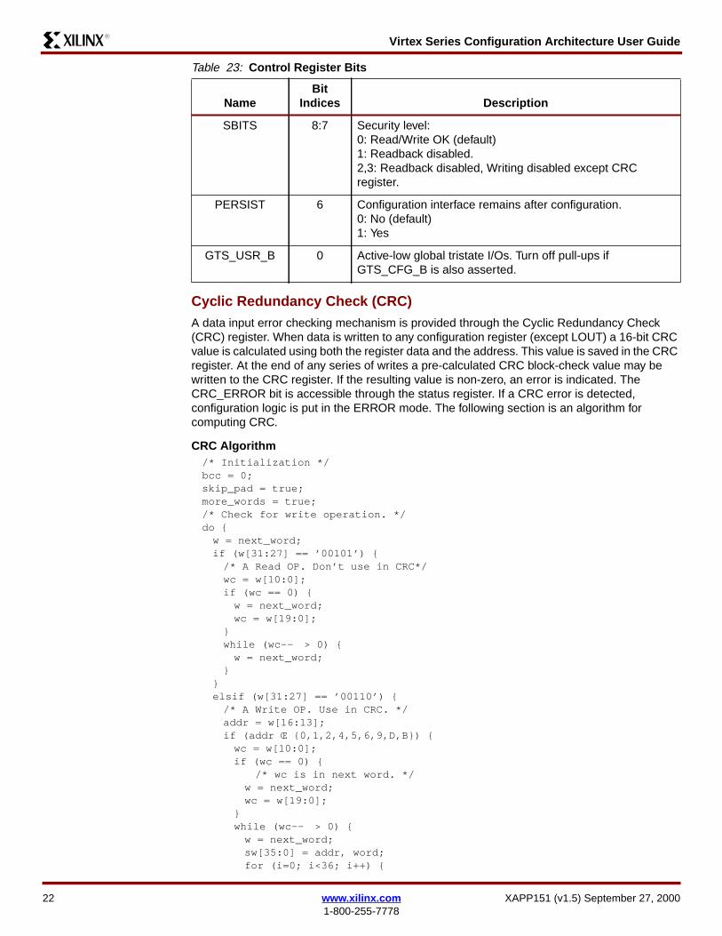
Virtex Series Configuration Architecture User GuideR13
Cyclic Redundancy Check (CRC)A data input error checking mechanism is provided through the Cyclic Redundancy Check(CRC) register When data is written to any configuration register (except LOUT) a 16-bit CRCvalue is calculated using both the register data and the address This value is saved in the CRCregister At the end of any series of writes a pre-calculated CRC block-check value may bewritten to the CRC register If the resulting value is non-zero an error is indicated TheCRC_ERROR bit is accessible through the status register If a CRC error is detectedconfiguration logic is put in the ERROR mode The following section is an algorithm forcomputing CRC
CRC Algorithm Initialization bcc = 0skip_pad = truemore_words = true Check for write operation do
w = next_wordif (w[3127] == rsquo00101rsquo)
A Read OP Donrsquot use in CRCwc = w[100]if (wc == 0)
w = next_wordwc = w[190]
while (wc-- gt 0)
w = next_word
elsif (w[3127] == rsquo00110rsquo)
A Write OP Use in CRC addr = w[1613]if (addr Π0124569DB)
wc = w[100]if (wc == 0)
wc is in next word w = next_wordwc = w[190]
while (wc-- gt 0)
w = next_wordsw[350] = addr wordfor (i=0 ilt36 i++)
Table 23 Control Register Bits
NameBit
Indices Description
SBITS 87 Security level0 ReadWrite OK (default)1 Readback disabled23 Readback disabled Writing disabled except CRCregister
PERSIST 6 Configuration interface remains after configuration0 No (default)1 Yes
GTS_USR_B 0 Active-low global tristate IOs Turn off pull-ups ifGTS_CFG_B is also asserted
22 wwwxilinxcom XAPP151 (v15) September 27 20001-800-255-7778
Virtex Series Configuration Architecture User GuideR13
x16 = bcc[15] XOR sw[i]x15 = bcc[14] XOR x16x2 = bcc[1] XOR x16bcc[150] =
x15bcc[132]x2bcc[0]x16 Note the bit order crc[150] = bcc[015]
else
Pad word - ignore
while (more_words)
Frame Address Register (FAR)The Frame Address Register (FAR) holds the address of the current frame The address isdivided into three parts the block type the major address and the minor address The blocktype field indicates whether the CLB or block RAM address space is used The command in thecommand register is executed each time the FAR is loaded with a new value
The major address selects the CLB or RAM column the minor address selects the frame withinthe column The minor address is incremented each time a full data frame is read from orwritten to the frame data register If the last frame within the CLB column is selected when theincrement occurs the major address is incremented and the minor address is reset to zerootherwise the minor address is incremented However the block RAM major address is notincremented automatically
See Figure 18 for the definitions of valid values for the block type field The FAR field definitionsare shown in Figure 19
Figure 17 CRC Calculation Register
Note the Block RAM Major Address is not incremented automatically To address a differentBlock RAM Content column the FAR must be loaded with the new Major Address
Type CodesCLB 00RAM 01
Figure 18 Block Type Codes
x151_17_021100
15141312111098765432
1013
01234526272829303101
Address 32-bit Data Word
CRC Calculation Register
CRC Data Input Register
CRC Register [310]
DATA_IN
SHIFT
23
16-bit CRC13150
0000 0000 0000 0000133116
1313
XAPP151 (v15) September 27 2000 wwwxilinxcom 231-800-255-7778
Virtex Series Configuration Architecture User GuideR13
Frame Data Input Register (FDRI)The Frame Data Input Register (FDRI) is used to load configuration frame data into a Virtexdevice
The Frame Data Register (FDR) is a shift register into which data is loaded prior to transfer tothe configuration memory Configuration data is written to the Virtex device by loading thecommand register with the WCFG command and then loading the FDR with at least two framesof 32-bit words
The write operation is pipelined such that the first frame of data is written to the configurationmemory while the second frame is being shifted in The last frame (the pad frame) is alwaysdummy data which is not actually written to the configuration memory Each frame write mustinclude enough 32 bit data words to load the frame fully There is one pad word at the end ofeach frame which is required for the pipelining hardware
Frame Data Output Register (FDRO)The Frame Data Output Register (FDRO) is for reading configuration data or captured datafrom the Virtex device a process called readback Readback is performed by loading thecommand register with the RCFG command and then addressing the FDRO with a readcommand
Frame Length Register (FLR)Near the beginning of the configuration bitstream the Frame Length Register (FLR) is writtenwith the length of a frame as measured in 32-bit words This length count is used to providesequencing information for the configuration read and write operations Note that the FLR mustbe written before any FDR operation works It is not necessary to set the FLR more than onceIf the number of bits in a frame is not evenly divisible by 32 the length count of the frame mustbe rounded up to the next highest integer The values for the FLR for all the current Virtexseries devices are given in Table 24
BlockType
Major Address(Column Address)
Minor Address(Frame Address)
31 30 29 28 27 26 25 24 23 22 21 20 19 18 17 16 15 14 13 12 11 10 9 8 7 6 5 4 3 2 1 00 0 0 0 0 x x x x x x x x x x x x x x x x x x 0 0 0 0 0 0 0 0 0
Notes1 Locations within fields containing a zero or one must have these values An X in a bit field indicates that the value is variable and must
be set2 Heavy vertical lines are used to separate fields Light vertical lines separate nibbles in the word
Figure 19 Frame Address Fields (FAR)
Note The FLR contains a value that is one less than the number of words that are read fromor written to a given frame This is because the extra word needed for pipelining is not counted
Table 24 Frame Length Register Value
Device Row times Col Frame Length Words per Frame FLR Value
XCV50E 16 times 24 384 12 11
XCV100E 20 times 30 448 14 13
XCV150 24 times 36 512 16 15
XCV200E 28 times 42 576 18 17
XCV300E 32 times 48 672 21 20
24 wwwxilinxcom XAPP151 (v15) September 27 20001-800-255-7778
Virtex Series Configuration Architecture User GuideR13
Legacy Output Register (LOUT)The Legacy Output Register (LOUT) is used for daisy chaining the configuration bitstream toother Xilinx devices Data written to the LOUT is serialized and appears on the DOUT pin
Mask Register (MASK)The Mask Register (MASK) is a mask register for writes to the CTL register A 1 in bit N of themask allows that bit position to be written in the CTL register The default value of the mask isall 0s
Status Register (STAT)The Status Register (STAT) is loaded with current values of several control or status signalsThe register can be read via the re-configuration block or via JTAG The fields in the Statusregister are illustrated in Figure 20 The values of the signals given in Table 25 on page 26 canbe read from the status register
XCV400E 40 times 60 800 25 24
XCV405E 40 times 60 800 25 24
XCV600E 48 times 72 960 30 29
XCV800 56 times 84 1088 34 33
XCV812E 56 times 84 1088 34 33
XCV1000E 64 times 96 1248 39 38
XCV1600E 72 times 108 1376 43 42
XCV2000E 80 times 120 1536 48 47
XCV2600E 92 times 138 1728 54 53
XCV3200E 104 times 156 1952 61 60
Table 24 Frame Length Register Value (Continued)
Device Row times Col Frame Length Words per Frame FLR Value
DO
NE
INIT
MO
DE
GH
IGH
_B
GS
R_B
GW
E_B
GT
S_C
FG
IN_E
RR
OR
LOC
K
CR
C_E
RR
OR
31 30 29 28 27 26 25 24 23 22 21 20 19 18 17 16 15 14 13 12 11 10 9 8 7 6 5 4 3 2 1 00 0 0 0 0 0 0 0 0 0 0 0 0 0 0 0 0 x x x x x x x x x x x x x x x
Notes1 An X in a bit field indicates that the value is variable2 Heavy vertical lines are used to separate fields Light vertical lines separate nibbles in the word
Figure 20 Status Register Fields
XAPP151 (v15) September 27 2000 wwwxilinxcom 251-800-255-7778
Virtex Series Configuration Architecture User GuideR13
ConfigurationInterface
There are two configuration interfaces to the Virtex devices mdash the bit-serial Boundary Scaninterface and the 8-bit byte-serial SelectMAP interface Conceptually XCV50 configurationdata appears as in Figure 21
Frames and words within frames are written in the same order in both configuration interfacesstarting with Frame 0 word 0 (the left-most in the picture) followed by word 1 etc Bits withineach word are written from left to right (MSB first) in the bit-serial configuration interfaces
Within the SelectMAP interface data is written a byte at a time A sample word is shown inFigure 22 The top row indicates the device pin names The bottom row indicates the bit indiceswithin a configuration word Byte 0 loads first followed by byte 1 et cetera The MSB of eachbyte (ie bits 31 23 15 and 7) is loaded on pin D0 The LSB of each byte (ie bits 24 16 8and 0) is loaded on pin D7
PartialReconfigurationof CLBs
Partial reconfiguration can be performed with and without shutting down the device Ifcontention occurs it is advised to go through a shutdown sequence prior to loadingconfiguration frames When shutting down the DONE pin will go active and pull low If this is notdesireable the DONE pin can be prevented from going low by selecting the DONE_CYCLE toKeep State (111) Similarly to prevent GSR from becoming active and reseting the currentstate the GSR_CYCLE can be set to Keep State When not shutting down changes occurframe by frame but is completely done by the end of the Last Frame packet (see Example 1)
Table 25 Status Register Bits
Name Bit Indices Description
DONE 14 Input from DONE pin
INIT 13 Value of INIT
MODE 1210 Value of M2 M1 M0 mode pins
GHIGH_B 9 0 = GHIGH_B asserted
GSR_B 8 0 = all flip-flops are ResetSet
GWE_B 7 1 = flip-flops and block RAM are write disabled
GTS_CFG 6 0 = IOs are tri-stated
IN_ERROR 5 Legacy input error
LOCK 41 Output from DLL lock signals 1 = DLL is locked
CRC_ERROR 0 Indicates that a CRC error has occurred
Data Frame 0 (11 words) Pad Word
hellip
Data Frame n (11 words) Pad WordPad Frame (12 words)
Figure 21 XCV50 Frame Padding for Reads
Figure 22 SelectMAP Byte and Bit Ordering
x151_22_021100
D0 D1 D2 D3 D4 D5 D6 D7 D0 D1 D2 D3 D4 D5 D6 D7 D0 D1 D2 D3 D4 D5 D6 D7 D0 D1 D2 D3 D4 D5 D6 D7
Byte 0 Byte 1 Byte 2 Byte 313
26 wwwxilinxcom XAPP151 (v15) September 27 20001-800-255-7778
Virtex Series Configuration Architecture User GuideR13
The DONE pin will not change in this case Figure 23 illustrates a typical shutdownreconfiguration in the CLB address space and restart sequence
Examples Several examples of reading and evaluating configuration data are provided to illustrate thefollowing
Figure 23 Typical Shutdown Reconfiguration in the CLB Address Spaceand Restart Sequence
FFFF FFFF Dummy WordAA99 5566 Sync Word Does not realign an already synchronized SelectMap port3001 2001 COR0080 FF2F Shutdown bit set optionally set bit 29 DRIVE_DONE
Alternately COR may be read bit 15 set and written back3000 8001 CMD0000 0005 Start Shutdown3000 8001 CMD0000 0007 Reset CRC0000 00000000 0000 Clock shutdown sequence0000 00000000 00003000 8001 CMD0000 0008 Assert GHIGH3000 8001 CMD0000 0001 Write Configuration3000 2001 FAR0--- ---- Block Type CLB (00) MajorMinor Address3000 4--- FDRI + Word Count if count is lt1024 Otherwise use TypeII Header
Write FRAME DATAIf CLB Frames are not written to non-consecutive addresses repeat FAR word followedby new MajorMinor Address followed by FDRI + Word Count and then Frame Data
3000 0001 Write CRC---- ---- CRC3000 8001 CMD0000 0003 LFRM3000 4--- FDRI + Word Count
Write PAD FRAME
3001 2001 COR0080 3F2D Default COR Options
Alternately COR may be read bit 15 cleared and written back3000 8001 CMD0000 0005 Begin Startup3000 0001 Write CRC---- ---- CRC
0000 00000000 0000 4 Dummy Words0000 00000000 0000
Example 1 Read and Write Semaphores in an XCV100 at CLB R1 C1 Slice 0 on page 28Example 2 Reading the Complete Configuration from an XCV50 on page 33
XAPP151 (v15) September 27 2000 wwwxilinxcom 271-800-255-7778
Virtex Series Configuration Architecture User GuideR13
Example 1 Read and Write Semaphores in an XCV100 at CLB R1 C1Slice 0Semaphores are a useful communication mechanism documented in XAPP 153 ldquoStatus andControl Semaphore Registers using Partial Reconfigurationrdquo Figure 24 shows an abstractionof a microprocessor writing control information to an FPGA and reading status informationOne convention for implementing semaphores in Virtex devices is to use two bits of a 16-bitdual-port RAM as illustrated in Figure 25 This occupies one CLB slice with the F-LUTimplementing the control semaphore and the status semaphore implemented in the G-LUTAddress 15 of the G-LUT is used for on-chip writes to the semaphore and address 14 of the F-LUT is used for on-chip reads Conversely the off-chip microprocessor is reading the G-LUT[15] and writing F-LUT[14]
Example 3 Read the Slice 0 G-LUT from CLB R1 C1 from the Complete Configuration of anXCV50 on page 34Example 4 Read the Slice 1 F-LUT from CLB R19 C16 from an XCV100 on page 36Example 5 Read All Bits in Slice 0 G-LUTs from CLB C2 and XCV50 on page 39Example 6 Read Block SelectRAM index 387 of RAM R2 C0 from an XCV100E on page 41
Figure 24 Semaphore Abstraction
x151_ 23_021400
Status13
Control13
MicroProcessor FPGA13
Semaphores13
28 wwwxilinxcom XAPP151 (v15) September 27 20001-800-255-7778
Virtex Series Configuration Architecture User GuideR13
Using a Semaphore Abstraction dual-port RAM ensures that the LUT SelectRAMs are placedin the CLB in a predictable manner When writing data to one or more LUT SelectRAMs or flip-flops on the device all bits in the frame must have valid configuration information This isassured by altering valid configurations from bitstream files or from frames read from a properlyconfigured Virtex device The latter approach is used in this example
Figure 25 Semaphore ReadWrite Implementation
Frame 47
15
14
47 46
47 46
x151_ 24_021100
Select Map
Frame 46
DING
F
13
D2D3D4 5D6 7D0D1 D D
1
111
0
111
Chip Interface
G F
13
XAPP151 (v15) September 27 2000 wwwxilinxcom 291-800-255-7778
Virtex Series Configuration Architecture User GuideR13
Attributes for this design are summarized in Table 26
From the equations in Table 7 on page 11 the values shown in Table 27 can be calculated
From off-chip for reading the G-LUT[15] bit read one frame (MNA=47) For writing the F-LUT[14] bit we show how to read then write one frame (MNA=46) as opposed to modifyingdata from a bitstream file (both are valid methods) The frames on the XCV100 contain 13 32-bit words and one pad word Remember that fm_st_wd is calculated assuming the entireconfiguration has been read However only the pad frame and then frames 46 and 47 fromMajor Address 30 are being read The desired bit is in Frame 1 word 1 which is word 15
The commands for reading both frames (and the pad frame) are given in Figure 26
Table 26 Design Attributes for Example 1
Attribute
G-LUT [15] F-LUT [14]
Read Read Write
Chip_Rows 20
Chip_Cols 30
FL 14
CLB_Row 1
CLB_Col 1
Slice 0
FG 1 0
lut_bit 15 14
RW 1 1 0
Table 27 Semaphore Example Variables Equations and Values
Variable Equation
Value(s)
G-LUT[15] F-LUT[14]
Read Read Write
MJA 1 le 302 rArr 30 ndash 1 times 2 + 2 30
MNA lut_bit + 32ndash 0 times () 47 46
fm_bit_idx 3 + 18 times 1 ndash FG + RW times 32 52 53 21
fm_st_wd 14 times (8 + (30 ndash 1) times 48+ 4647) +RW times (14 +1)= 14 times (1400 + 4647) + 14 times RW= 19600 + 14 times 4647 + 14 times RW
20272 20258 20244
fm_wd floor (2032) 1 1 0
fm_wd_bit_idx 31 + 32 times 110 ndash 525321 11 10 10
30 wwwxilinxcom XAPP151 (v15) September 27 20001-800-255-7778
Virtex Series Configuration Architecture User GuideR13
The 42 words read are shown in Figure 27 F-LUT[14] is in the second frame (frame=1word=1) at bit 10 The value read is a 1 but because the LUT bits are inverted the logic valueis zero G-LUT[15] is in word one of the third data frame (frame=2 word=1) at bit 11The valueread is a 1 which is a logic zero
InstructionData
Hex 31 30 29 28 27 26 25 24 23 22 21 20 19 18 17 16 15 14 13 12 11 10 9 8 7 6 5 4 3 2 1 0
Sync Word AA99 5566 1 0 1 0 1 0 1 0 1 0 0 1 1 0 0 1 0 1 0 1 0 1 0 1 0 1 1 0 0 1 1 0
Write next (1) word to FAR 3000 2001 0 0 1 1 0 0 0 0 0 0 0 0 0 0 0 0 0 0 1 0 0 0 0 0 0 0 0 0 0 0 0 1
CLB MJA=30 MNA=46 003C 5800 0 0 0 0 0 0 0 0 0 0 1 1 1 1 0 0 0 1 0 1 1 1 0 0 0 0 0 0 0 0 0 0
Write next word to CMD 3000 8001 0 0 1 1 0 0 0 0 0 0 0 0 0 0 0 0 1 0 0 0 0 0 0 0 0 0 0 0 0 0 0 1
Register value for RCFG 0000 0004 0 0 0 0 0 0 0 0 0 0 0 0 0 0 0 0 0 0 0 0 0 0 0 0 0 0 0 0 0 1 0 0
Read from FDRO 2800 602A 0 0 1 0 1 0 0 0 0 0 0 0 0 0 0 0 0 1 1 0 0 0 0 0 0 0 1 0 1 0 1 0
Flush pipe 0000 0000 0 0 0 0 0 0 0 0 0 0 0 0 0 0 0 0 0 0 0 0 0 0 0 0 0 0 0 0 0 0 0 0
(read 42 words)
Notes1 Binary data is grouped in two ways for ease of interpretation Thin vertical lines separate nibble boundaries Heavy vertical lines
separate field boundaries
Figure 26 Commands to Read Two Data Frames
XAPP151 (v15) September 27 2000 wwwxilinxcom 311-800-255-7778
Virtex Series Configuration Architecture User GuideR13
To write to the F-LUT semaphore start with the second data frame (frame=1) that was justread Words 1 - 13 of that frame will become words 0 - 12 of the frame to be written Word 13of this new frame is a pad word and can have any value (typically 0 is chosen) In this newframe set bit 11 of word 0 (zero) to the desired value of the semaphore A pad frame mustfollow the data frame The commands from Figure 28 write these two frames into the device atthe proper location
Frame Word 31 30 29 28 27 26 25 24 23 22 21 20 19 18 17 16 15 14 13 12 11 10 9 8 7 6 5 4 3 2 1 0
0
0 1 1 1 1 1 1 1 1 1 1 1 1 1 1 1 1 1 1 1 1 1 1 1 1 1 1 1 1 1 1 1 1
1 1 1 1 1 1 1 1 1 1 1 1 1 1 1 1 1 1 1 1 1 1 1 1 1 1 1 1 1 1 1 1 1
2 1 1 1 1 1 1 1 1 1 1 1 1 1 1 1 1 1 1 1 1 1 1 1 1 1 1 1 1 1 1 1 1
3 1 1 1 1 1 1 1 1 1 1 1 1 1 1 1 1 1 1 1 1 1 1 1 1 1 1 1 1 1 1 1 1
4 1 1 1 1 1 1 1 1 1 1 1 1 1 1 1 1 1 1 1 1 1 1 1 1 1 1 1 1 1 1 1 1
5 1 1 1 1 1 1 1 1 1 1 1 1 1 1 1 1 1 1 1 1 1 1 1 1 1 1 1 1 1 1 1 1
6 1 1 1 1 1 1 1 1 1 1 1 1 1 1 1 1 1 1 1 1 1 1 1 1 1 1 1 1 1 1 1 1
7 1 1 1 1 1 1 1 1 1 1 1 1 1 1 1 1 1 1 1 1 1 1 1 1 1 1 1 1 1 1 1 1
8 1 1 1 1 1 1 1 1 1 1 1 1 1 1 1 1 1 1 1 1 1 1 1 1 1 1 1 1 1 1 1 1
9 1 1 1 1 1 1 1 1 1 1 1 1 1 1 1 1 1 1 1 1 1 1 1 1 1 1 1 1 1 1 1 1
10 1 1 1 1 1 1 1 1 1 1 1 1 1 1 1 1 1 1 1 1 1 1 1 1 1 1 1 1 1 1 1 1
11 1 1 1 1 1 1 1 1 1 1 1 1 1 1 1 1 1 1 1 1 1 1 1 1 1 1 1 1 1 1 1 1
12 1 1 1 1 1 1 1 1 1 1 1 1 1 1 1 1 1 1 1 1 1 1 1 1 1 1 1 1 1 1 1 1
13 1 1 1 1 1 1 1 1 1 1 1 1 1 1 1 1 1 1 1 1 1 1 1 1 1 1 1 1 1 1 1 1
1
0 0 0 0 0 0 0 0 0 0 0 0 0 0 0 0 0 0 0 0 0 0 0 0 0 0 0 0 0 0 0 0 0
1 1 0 0 0 0 0 0 0 0 0 0 0 1 0 0 0 0 1 1 0 1 1 0 0 0 0 0 0 0 0 0 0 F[14]
2 1 1 1 1 1 0 1 1 0 0 0 0 1 1 1 1 0 0 1 1 1 1 1 0 1 1 0 0 0 0 0 0
3 0 0 0 0 1 1 1 1 1 0 1 1 0 0 0 0 0 0 0 0 0 0 1 1 1 1 1 0 1 1 0 0
4 0 0 0 0 0 0 0 0 1 1 1 1 0 0 0 0 0 0 0 0 0 0 0 0 0 0 1 1 1 1 1 0
5 1 1 0 0 1 1 0 0 0 0 0 0 1 1 0 0 1 0 1 1 0 0 0 0 0 0 0 0 0 0 1 1
6 1 1 1 0 1 1 0 0 0 0 0 0 1 1 1 0 1 1 1 0 1 0 1 1 0 0 0 0 0 0 0 0
7 0 0 1 1 1 1 1 0 1 1 0 0 0 0 1 1 0 0 0 0 1 1 1 1 1 0 1 1 0 0 0 0
8 0 0 0 0 0 0 1 1 1 1 1 0 0 0 0 0 0 0 0 0 0 0 0 0 1 1 1 1 1 0 1 1
9 0 0 0 0 0 0 0 0 0 0 1 1 0 0 0 0 1 1 0 0 0 0 0 0 0 0 0 0 1 1 1 1
10 1 0 1 1 0 0 0 0 0 0 0 0 1 0 1 1 1 1 1 0 1 1 0 0 0 0 0 0 0 0 0 0
11 1 1 1 1 1 0 1 1 0 0 0 0 1 1 1 1 0 0 1 1 1 1 1 0 1 1 0 0 0 0 0 0
12 0 0 0 0 1 1 0 1 1 0 1 1 0 0 0 0 0 0 0 0 0 0 1 1 1 1 1 0 0 0 0 0
13 0 0 0 0 0 0 1 1 0 1 0 1 0 0 0 0 0 0 0 0 0 0 0 0 0 0 0 0 0 0 0 0
2
0 0 0 0 0 0 0 0 0 0 0 0 0 0 0 0 0 0 0 0 0 0 0 0 0 0 0 0 0 0 0 0 0
1 1 0 1 0 0 0 0 0 0 0 0 1 1 0 1 0 1 1 1 0 1 1 0 0 0 0 0 0 0 0 0 0 G[15]
2 1 1 1 1 1 1 1 1 0 0 0 0 1 1 1 1 0 0 1 1 1 1 1 1 1 1 0 0 0 0 0 0
3 0 0 0 0 1 1 1 1 1 1 1 1 0 0 0 0 0 0 0 0 0 0 1 0 1 1 1 1 1 1 0 0
4 0 0 0 0 0 0 0 0 1 1 1 1 0 0 0 0 0 0 0 0 0 0 0 0 0 0 1 1 1 1 1 1
5 1 1 0 0 0 0 0 0 0 0 0 0 1 1 0 0 1 1 1 1 0 0 1 0 0 0 0 0 0 0 1 1
6 1 1 1 1 1 1 0 0 0 0 0 0 1 1 1 1 1 1 1 1 1 1 1 1 0 0 0 0 0 0 0 0
7 0 0 1 1 1 1 1 1 1 1 0 0 0 0 1 1 0 0 0 0 1 1 1 1 1 1 1 1 0 0 0 0
8 0 0 0 0 0 0 1 1 1 1 1 1 0 0 0 0 0 0 0 0 0 0 0 0 1 1 1 1 1 1 1 1
9 0 0 0 0 0 0 0 0 0 0 1 1 0 0 0 0 1 1 0 0 0 0 0 0 0 0 0 0 1 1 1 1
10 1 1 1 1 0 0 0 0 0 0 0 0 1 1 1 1 1 1 1 1 1 1 0 0 0 0 0 0 0 0 0 0
11 1 1 1 1 1 1 1 1 0 0 0 0 1 1 1 1 0 0 1 1 1 1 1 1 1 1 0 0 0 0 0 0
12 0 0 0 0 1 1 0 1 1 1 1 1 0 0 0 0 0 0 0 0 0 0 1 1 1 1 1 0 1 0 0 0
13 0 0 0 0 0 1 1 0 0 1 1 1 0 0 0 0 0 0 0 0 0 0 0 0 0 0 0 0 0 0 0 0
Figure 27 Three Frames Containing the Semaphores
32 wwwxilinxcom XAPP151 (v15) September 27 20001-800-255-7778
Virtex Series Configuration Architecture User GuideR13
Example 2 Reading the Complete Configuration from an XCV50Steps
1 If flip-flop values are needed clock the on-chip signal CAPTURE to capture flip-flopvalues See the Xilinx Libraries Guide for use of the CAPTURE_VIRTEX cell
2 Write the starting frame address (CLB MJA=0 MNA=0) into the FAR
3 Write the RCFG command to the CMD register
4 Address the FDRO register with a READ operation and word count equal to the number of32-bit words in the CLB frames plus one pad frame
5 Read the data following the timing diagrams in the SelectMAP interface section
6 Write the address for RAM block 0 to the FAR
7 Address the FDRO register with a read operation and word count equal to the number of32-bit words in the RAM block plus one pad frame
8 Read the data
9 Write the address for RAM block 1 to the FAR
10 Address the FDRO register with a read operation and word count equal to the number of32-bit words in the RAM block plus one pad frame
11 Read the data
When using SelectMAP mode to read data words from the Virtex device de-assert CS de-assert WRITE assert CS then clock the data out When using JTAG load the JTAG IR
InstructionData
Hex 31 30 29 28 27 26 25 24 23 22 21 20 19 18 17 16 15 14 13 12 11 10 9 8 7 6 5 4 3 2 1 0
Sync Word AA995566
1 0 1 0 1 0 1 0 1 0 0 1 1 0 0 1 0 1 0 1 0 1 0 1 0 1 1 0 0 1 1 0
Write next (1) word to FAR 30002001
0 0 1 1 0 0 0 0 0 0 0 0 0 0 0 0 0 0 1 0 0 0 0 0 0 0 0 0 0 0 0 1
MJA=30 MNA=46 003C5C00
0 0 0 0 0 0 0 0 0 0 1 1 1 1 0 0 0 1 0 1 1 1 0 0 0 0 0 0 0 0 0 0
Write next word to CMD 30008001
0 0 1 1 0 0 0 0 0 0 0 0 0 0 0 0 1 0 0 0 0 0 0 0 0 0 0 0 0 0 0 1
Register value for WCFG 00000001
0 0 0 0 0 0 0 0 0 0 0 0 0 0 0 0 0 0 0 0 0 0 0 0 0 0 0 0 0 0 0 1
Write 28 words to FDRI 3000401C
0 0 1 1 0 0 0 0 0 0 0 0 0 0 0 0 0 1 0 0 0 0 0 0 0 0 0 1 1 1 0 0
Data Word 0 A01AEC00
1 0 1 0 0 0 0 0 0 0 0 1 1 0 1 0 1 1 1 0 1 1 0 0 0 0 0 0 0 0 0 0
Data Word 1 FF0F3FC0
1 1 1 1 1 1 1 1 0 0 0 0 1 1 1 1 0 0 1 1 1 1 1 1 1 1 0 0 0 0 0 0
Data Word 2 0FF002FC
0 0 0 0 1 1 1 1 1 1 1 1 0 0 0 0 0 0 0 0 0 0 1 0 1 1 1 1 1 1 0 0
hellip hellip hellip
Data Word 27 00000000
0 0 0 0 0 0 0 0 0 0 0 0 0 0 0 0 0 0 0 0 0 0 0 0 0 0 0 0 0 0 0 0
Notes1 Binary data is grouped in two ways for ease of interpretation Thin vertical lines separate nibble boundaries Heavy
vertical lines separate field boundaries
Figure 28 Commands to Write a Semaphore Value
XAPP151 (v15) September 27 2000 wwwxilinxcom 331-800-255-7778
Virtex Series Configuration Architecture User GuideR13
(instruction register) with the CFG_OUT instruction Then go to the SDR (Shift-DR) state andshift the data out (See Figure 29)
Example 3 Read the Slice 0 G-LUT from CLB R1 C1 from the CompleteConfiguration of an XCV50The commands for reading the bitstream from the Virtex device are given in Example 1 Readand Write Semaphores in an XCV100 at CLB R1 C1 Slice 0 on page 28 Using an XCV50device the independent attributes are show in Table 28
InstructionData
Hex 31 30 29 28 27 26 25 24 23 22 21 20 19 18 17 16 15 14 13 12 11 10 9 8 7 6 5 4 3 2 1 0
Sync Word AA99 5566 1 0 1 0 1 0 1 0 1 0 0 1 1 0 0 1 0 1 0 1 0 1 0 1 0 1 1 0 0 1 1 0
Write next word to FAR 3000 2001 0 0 1 1 0 0 0 0 0 0 0 0 0 0 0 0 0 0 1 0 0 0 0 0 0 0 0 0 0 0 0 1
CLB MJA=0 MNA=0 0000 0000 0 0 0 0 0 0 0 0 0 0 0 0 0 0 0 0 0 0 0 0 0 0 0 0 0 0 0 0 0 0 0 0
Write next word to CMDregister
3000 8001 0 0 1 1 0 0 0 0 0 0 0 0 0 0 0 0 1 0 0 0 0 0 0 0 0 0 0 0 0 0 0 1
Register value for RCFG 0000 0004 0 0 0 0 0 0 0 0 0 0 0 0 0 0 0 0 0 0 0 0 0 0 0 0 0 0 0 0 0 1 0 0
Read from FDRO register 2800 6000 0 0 1 0 1 0 0 0 0 0 0 0 0 0 0 0 0 1 1 0 0 0 0 0 0 0 0 0 0 0 0 0
15876 words 4800 3E04 0 1 0 0 1 0 0 0 0 0 0 0 0 0 0 0 0 0 1 1 1 1 1 0 0 0 0 0 0 1 0 0
Flush pipe 0000 0000 0 0 0 0 0 0 0 0 0 0 0 0 0 0 0 0 0 0 0 0 0 0 0 0 0 0 0 0 0 0 0 0
(Read 15876 words)Write to FAR register 3000 2001 0 0 1 1 0 0 0 0 0 0 0 0 0 0 0 0 0 0 1 0 0 0 0 0 0 0 0 0 0 0 0 1
RAM MJA=0 MNA=0 0200 0000 0 0 0 0 0 0 1 0 0 0 0 0 0 0 0 0 0 0 0 0 0 0 0 0 0 0 0 0 0 0 0 0
Read 780 words fromFDRO reg
2800 630C 0 0 1 0 1 0 0 0 0 0 0 0 0 0 0 0 0 1 1 0 0 0 1 1 0 0 0 0 1 1 0 0
Flush pipe 0000 0000 0 0 0 0 0 0 0 0 0 0 0 0 0 0 0 0 0 0 0 0 0 0 0 0 0 0 0 0 0 0 0 0
(Read 780 words)Write to FAR register 3000 2001 0 0 1 1 0 0 0 0 0 0 0 0 0 0 0 0 0 0 1 0 0 0 0 0 0 0 0 0 0 0 0 1
RAM MJA=1 MNA=0 0202 0000 0 0 0 0 0 0 1 0 0 0 0 0 0 0 1 0 0 0 0 0 0 0 0 0 0 0 0 0 0 0 0 0
Read 780 words fromFDRO reg
2800 630C 0 0 1 0 1 0 0 0 0 0 0 0 0 0 0 0 0 1 1 0 0 0 1 1 0 0 0 0 1 1 0 0
Flush pipe 0000 0000 0 0 0 0 0 0 0 0 0 0 0 0 0 0 0 0 0 0 0 0 0 0 0 0 0 0 0 0 0 0 0 0
(Read 780 words)
Figure 29 Example 2 - Read Complete Configuration for XCV50
Table 28 XCV50 Independent Attributes
Independent Attributes Values
Chip_Rows 16
Chip_Cols 24
FL 12
CLB_Row 1
CLB_Col 1
FG 1
Slice 0
RW 1
34 wwwxilinxcom XAPP151 (v15) September 27 20001-800-255-7778
Virtex Series Configuration Architecture User GuideR13
From the equations given earlier in Table 7 calculating the range of values for fm_st_wdindicates that the word 13740 of the configuration is the starting word of the 12-word (FL=12)frame containing bit 0 of the G-LUT in Slice 0 of CLB R1C1 (Table 29)
The configuration bits for the given frame are as follows G-LUT[0] is in fm_wd=0 at bit 11
All 16 LUT SelectRAM bits are in the following words at the same bit index 11
Table 29 Variables Equations and Values for Slice 0 G-LUT
Variables Equations Values
MJA 1 le 242 rArr 24 ndash 1times 2 + 2 24
MNA 0 times (hellip) + lut_bit + 32 0 321 332 343 35
4 365 376 387 39
8 409 41
10 4211 43
12 4413 4514 4615 47
fm_bit_idx 3 + 18 times 1 ndash1 + RW times 32 52
fm_st_wd 12 times (8+ (24 ndash1) times 48 + [3247]) +1 x 12= 12 times (1112 + [3247]) +12= 13356 + 12 times 3247]
1374013920
fm_wd floor(5232) 1
fm_wd_bit_idx 31 + 32 ndash 52 11
BitstreamWord
Frame 32-bit Word FrameWord31 30 29 28 27 26 25 24 23 22 21 20 19 18 17 16 15 14 13 12 11 10 9 8 7 6 5 4 3 2 1 0
13740 0 0 0 0 0 0 0 0 0 0 0 0 0 0 0 0 0 0 0 0 0 0 0 0 0 0 0 0 0 0 0 0 013741 0 0 1 0 1 0 0 0 0 0 0 0 0 1 0 1 0 1 0 0 1 1 1 0 0 0 0 0 0 0 0 0 113742 1 0 1 1 0 0 1 1 0 0 0 0 0 0 0 0 0 0 1 0 1 1 0 0 1 1 0 0 0 0 0 0 213743 0 0 0 0 1 0 1 1 0 0 1 1 0 0 0 0 0 0 0 0 0 0 1 0 1 1 0 0 1 1 0 0 313744 0 0 0 0 0 0 0 0 1 0 1 1 0 0 1 1 0 0 0 0 0 0 0 0 0 0 1 0 1 1 0 0 413745 1 1 0 0 0 0 0 0 0 0 0 0 1 0 1 1 0 0 1 1 0 0 0 0 0 0 0 0 0 0 1 0 513746 1 1 0 0 1 1 0 0 0 0 0 0 0 0 0 0 1 0 1 1 0 0 1 1 0 0 0 0 0 0 0 0 613747 0 0 1 0 1 1 0 0 1 1 0 0 0 0 0 0 0 0 0 0 1 0 1 1 0 0 1 1 0 0 0 0 713748 0 0 0 0 0 0 1 0 1 1 0 0 1 1 0 0 0 0 0 0 0 0 0 0 1 0 1 1 0 0 1 1 813749 0 0 0 0 0 0 0 0 0 0 1 0 1 1 0 0 1 1 0 0 0 0 0 0 0 0 0 0 1 0 1 1 913750 0 0 1 1 0 0 0 0 0 0 0 0 0 0 1 0 1 1 0 0 1 0 1 0 0 0 0 0 0 0 0 0 1013751 0 1 0 1 0 0 0 0 0 0 0 0 0 0 0 0 0 0 0 0 0 0 0 0 0 0 0 0 0 0 0 0 11
Figure 30 Configuration Bits for Slice 0 CLB R1C1 G-LUT [0]
XAPP151 (v15) September 27 2000 wwwxilinxcom 351-800-255-7778
Virtex Series Configuration Architecture User GuideR13
The 16 bits are LUT[150]=0111111111111111 The LUT SelectRAM bits are inverted from theirlogic values The ldquologicalrdquo contents are LUT[150]=1000000000000000 Thus this G-LUTimplements a 4-input AND function
Example 4 Read the Slice 1 F-LUT from CLB R19 C16 from an XCV100Commands for reading the bitstream from the Virtex device are given in Figure 32 Use thefollowing independent attributes to find the given F-LUT
From the equations in Table 7 on page 11 calculating fm_st_wd indicates the starting wordwith respect to a configuration that starts at MJA=0 MNA=0 Because the frames we are
BitstreamWord
Frame 32-bit Word
LUT Bit31 30 29 28 27 26 25 24 23 22 21 20 19 18 17 16 15 14 13 12 11 10 9 8 7 6 5 4 3 2 1 0
13741 0 0 1 0 1 0 0 0 0 0 0 0 0 1 0 1 0 1 0 0 1 1 1 0 0 0 0 0 0 0 0 0 0
13753 1 0 1 0 0 0 0 0 0 0 0 0 0 0 0 1 0 0 0 1 1 1 0 0 0 0 0 0 0 0 0 0 1
13765 1 0 1 0 1 0 0 0 0 0 0 0 1 0 0 0 0 0 0 1 1 1 1 0 0 0 0 0 0 0 0 0 2
13777 0 0 0 0 1 0 0 0 0 0 0 1 1 1 0 1 1 0 1 0 1 1 0 0 0 0 0 0 0 0 0 0 3
13789 0 1 0 0 0 0 0 0 0 0 0 0 0 1 0 1 1 1 1 1 1 1 1 0 0 0 0 0 0 0 0 0 4
13801 1 0 1 0 1 0 0 0 0 0 0 1 0 0 0 1 1 0 0 1 1 1 0 0 0 0 0 0 0 0 0 0 5
13813 0 0 0 1 0 0 0 0 0 0 0 0 0 0 0 0 1 0 0 1 1 1 0 0 0 0 0 0 0 0 0 0 6
13825 0 1 1 0 1 0 0 0 0 0 0 1 0 1 0 0 1 1 0 0 1 1 0 0 0 0 0 0 0 0 0 0 7
13837 1 0 1 1 1 0 0 0 0 0 0 1 0 1 0 1 1 0 0 0 1 1 0 0 0 0 0 0 0 0 0 0 8
13849 1 0 0 0 0 0 0 0 0 0 0 0 0 0 0 0 1 1 1 0 1 1 0 0 0 0 0 0 0 0 0 0 9
13861 1 0 0 0 0 0 0 0 0 0 0 1 0 0 0 0 1 1 1 1 1 1 1 0 0 0 0 0 0 0 0 0 10
13873 1 0 0 0 0 0 0 1 0 0 0 0 0 1 0 0 0 1 1 0 1 1 0 0 0 1 0 0 0 0 0 0 11
13885 1 0 0 0 0 0 0 0 0 0 0 0 0 1 0 1 0 0 1 0 1 1 0 0 0 0 0 0 0 0 0 0 12
13897 0 0 0 0 1 0 0 0 0 0 0 0 0 1 0 0 0 0 0 0 1 1 0 0 0 0 0 0 0 0 0 0 13
13909 1 0 0 0 0 0 0 0 0 0 0 0 1 1 0 1 0 1 1 0 1 1 0 0 0 0 0 0 0 0 0 0 14
13921 1 0 1 0 0 0 0 0 0 0 0 1 1 1 0 1 1 1 1 1 0 1 0 0 0 0 0 0 0 0 0 0 15
Figure 31 Location of all 16 LUT SelectRAM Bits
Table 30 Virtex Bitstream Command Attributes
Independent Attributes Values
Chip_Rows 20
Chip_Cols 30
FL 14
CLB_Row 19
CLB_Col 16
FG 0
Slice 1
RW 1
36 wwwxilinxcom XAPP151 (v15) September 27 20001-800-255-7778
Virtex Series Configuration Architecture User GuideR13
interested in start at MJA=1 MNA=0 which is fm_st_wd = 126 so the first 126 words are notneeded (0ndash125) Therefore to find the given Slice 1 F-LUT see Table 31
Sixteen frames need to be read one for each bit in the LUT SelectRAM The bits in LUTSelectRAMs in Slice 1 occur in the opposite order that they do for Slice 0 LUT SelectRAMs
Frames are read sequentially with ascending addresses If read in LUT bit order LUT[0]LUT[1] hellip LUT[15] These are stored in descending addresses which require 16 separateread operations each reading one data frame and one pad frame However if read inascending address order LUT[15] LUT[14] hellip LUT[0] all 16 data frames are read with asingle read operation This requires only one pad frame for all 16 frames Thus it takes lesstime to read ascending frames starting at MJA=1 MNA=0 and finishing with frame MJA=1MNA=15 The frames in the XCV100 contain 14 32-bit words and a single pad wordCommands for reading only the F-LUT data are given in Figure 32
Table 31 Variables Equations and Values for Slice 1 F-LUT
Variables Equations Values
MJA 16 gt 302 rArr 2times16 ndash 30 ndash1 1
MNA lut_bit + 32 ndash Slice times (2 times lut_bit +17)= [015] + 32 ndash (2 times [015] + 17)= 15 ndash [015]
0 151 142 133 12
4 115 106 97 8
8 79 6
10 511 4
12 313 214 115 0
fm_bit_idx 3 + 18 times 19 ndash 0+ 32 377
fm_st_wd 14 times (8 + (1ndash 1) times 48 + [150]) +1 times 14= 14 times (8 + [150]) +14= 126 + 14 times [150]
= 336126
fm_wd floor(37732) 11
fm_wd_bit_idx 31 + 32 times 11 ndash 377 6
XAPP151 (v15) September 27 2000 wwwxilinxcom 371-800-255-7778
Virtex Series Configuration Architecture User GuideR13
The 377th bit of each frame is the bit in the F-LUT This LUT SelectRAM bit is in the framersquosword index 11 bit index 6
The configuration bits for the given frame in Figure 33 are as follows LUT Bit 15 is in MJA=1MNA=0 fm_wd=11 at bit 6
LUT bit 0 is in MJA=1 MNA=15 fm_wd=11 at bit 6
InstructionData
Hex 31 30 29 28 27 26 25 24 23 22 21 20 19 18 17 16 15 14 13 12 11 10 9 8 7 6 5 4 3 2 1 0
Sync Word AA99 5566 1 0 1 0 1 0 1 0 1 0 0 1 1 0 0 1 0 1 0 1 0 1 0 1 0 1 1 0 0 1 1 0
Write next (1) word to FAR 3000 2001 0 0 1 1 0 0 0 0 0 0 0 0 0 0 0 0 0 0 1 0 0 0 0 0 0 0 0 0 0 0 0 1
CLB MJA = 1 MNA = 0 0002 0000 0 0 0 0 0 0 0 0 0 0 0 0 0 0 1 0 0 0 0 0 0 0 0 0 0 0 0 0 0 0 0 0
Write next word to CMD 3000 8001 0 0 1 1 0 0 0 0 0 0 0 0 0 0 0 0 1 0 0 0 0 0 0 0 0 0 0 0 0 0 0 1
Register value for RCFG 0000 0004 0 0 0 0 0 0 0 0 0 0 0 0 0 0 0 0 0 0 0 0 0 0 0 0 0 0 0 0 0 1 0 0
Read from FDRO 2800 60EE 0 0 1 0 1 0 0 0 0 0 0 0 0 0 0 0 0 1 1 0 0 0 0 0 1 1 1 0 1 1 1 0
Flush pipe 0000 0000 0 0 0 0 0 0 0 0 0 0 0 0 0 0 0 0 0 0 0 0 0 0 0 0 0 0 0 0 0 0 0 0
(Read 238 words)
Figure 32 Commands to read Slice 1 F-LUT
Frame WordFrame 32-bit Word
31 30 29 28 27 26 25 24 23 22 21 20 19 18 17 16 15 14 13 12 11 10 9 8 7 6 5 4 3 2 1 0
0 0 0 0 0 0 0 0 0 0 0 0 0 0 0 0 0 0 0 0 0 0 0 0 0 0 0 0 0 0 0 0 0
1 1 1 0 0 0 0 0 0 0 0 0 0 0 1 0 1 1 1 1 1 1 1 0 0 0 0 0 0 0 0 0 0
2 1 1 1 1 1 1 1 1 0 0 0 0 0 0 0 0 0 0 1 1 1 1 1 1 1 1 0 0 0 0 0 0
3 0 0 0 0 1 1 1 1 1 1 1 1 0 0 0 0 0 0 0 0 0 0 1 1 1 1 1 1 1 1 0 0
4 0 0 0 0 0 0 0 0 1 1 1 1 1 1 1 1 0 0 0 0 0 0 0 0 0 0 1 1 1 1 1 1
5 1 1 0 0 0 0 0 0 0 0 0 0 1 1 1 1 1 1 1 1 0 0 0 0 0 0 0 0 0 0 1 1
6 1 1 1 1 1 1 0 0 0 0 0 0 0 0 0 0 1 1 1 1 1 1 1 1 0 0 0 0 0 0 0 0
7 0 0 1 1 1 1 1 1 1 1 0 0 0 0 0 0 0 0 0 0 1 1 1 1 1 1 1 1 0 0 0 0
8 0 0 0 0 0 0 1 1 1 1 1 1 1 1 0 0 0 0 0 0 0 0 0 0 1 1 1 1 1 1 1 1
9 0 0 0 0 0 0 0 0 0 0 1 1 1 1 1 1 1 1 0 0 0 0 0 0 0 0 0 0 1 1 1 1
10 1 1 1 1 0 0 0 0 0 0 0 0 0 0 1 1 1 1 1 1 1 1 0 0 0 0 0 0 0 0 0 0
11 1 1 1 1 1 1 1 1 0 0 0 0 0 0 0 0 0 0 1 1 1 1 1 1 1 0 0 0 0 0 0 0
12 0 0 0 0 1 1 1 1 1 1 1 1 0 0 0 0 0 0 0 0 0 0 1 1 1 1 1 1 0 0 0 0
13 0 0 0 0 0 0 0 0 0 1 1 1 0 0 0 0 0 0 0 0 0 0 1 1 1 1 1 1 0 0 0 0
Figure 33 Frame Containing F-LUT[15]
Bit streamWord
Frame 32-bit WordFmWd31 30 29 28 27 26 25 24 23 22 21 20 19 18 17 16 15 14 13 12 11 10 9 8 7 6 5 4 3 2 1 0
336 0 0 0 0 0 0 0 0 0 0 0 0 0 0 0 0 0 0 0 0 0 0 0 0 0 0 0 0 0 0 0 0 0337 0 1 0 0 1 0 0 0 0 0 0 1 0 1 0 0 1 1 0 0 1 1 0 0 0 0 0 0 0 0 0 0 1338 1 0 1 1 0 0 1 1 0 0 0 0 0 0 0 0 0 0 1 0 1 1 0 0 1 1 0 0 0 0 0 0 2339 0 0 0 0 1 0 1 1 0 0 1 1 0 0 0 0 0 0 0 0 0 0 1 0 1 1 0 0 1 1 0 0 3340 0 0 0 0 0 0 0 0 1 0 1 1 0 0 1 1 0 0 0 0 0 0 0 0 0 0 1 0 1 1 0 0 4341 1 1 0 0 0 0 0 0 0 0 0 0 1 0 1 1 0 0 1 1 0 0 0 0 0 0 0 0 0 0 1 0 5342 1 1 0 0 1 1 0 0 0 0 0 0 0 0 0 0 1 0 1 1 0 0 1 1 0 0 0 0 0 0 0 0 6343 0 0 1 0 1 1 0 0 1 1 0 0 0 0 0 0 0 0 0 0 1 0 1 1 0 0 1 1 0 0 0 0 7
Figure 34 Frame Containing F-LUT [0]
38 wwwxilinxcom XAPP151 (v15) September 27 20001-800-255-7778
Virtex Series Configuration Architecture User GuideR13
For the sake of brevity here are the sixteen 11th words in the order they appear in thebitstream
The bits are LUT[150]=0111111111111111 The LUT SelectRAM bits are inverted from thelogic sense The logical contents are LUT[150]=1000000000000000 Thus this F-LUTimplements a 4-input AND gate
Example 5 Read All Bits in Slice 0 G-LUTs from CLB C2 and XCV50Given the following attributes the necessary values to find the G-LUT data can be computed
344 0 0 0 0 0 0 1 0 1 1 0 0 1 1 0 0 0 0 0 0 0 0 0 0 1 0 1 1 0 0 1 1 8345 0 0 0 0 0 0 0 0 0 0 1 0 1 1 0 0 1 1 0 0 0 0 0 0 0 0 0 0 1 0 1 1 9346 0 0 1 1 0 0 0 0 0 0 0 0 0 0 1 0 1 1 0 0 1 1 0 0 0 0 0 0 0 0 0 0 10347 1 1 1 1 1 0 1 1 0 0 0 0 0 0 0 0 0 0 1 0 1 1 1 0 1 1 0 1 0 0 0 0 11348 0 0 0 0 1 1 1 0 1 0 1 1 0 0 0 0 0 0 0 0 0 0 1 1 1 1 0 1 0 0 0 0 12349 0 0 0 0 0 1 0 0 0 0 1 0 0 0 0 0 0 0 0 0 0 0 0 0 0 0 0 0 0 0 0 0 13
Bit streamWord
Frame 32-bit WordFmWd31 30 29 28 27 26 25 24 23 22 21 20 19 18 17 16 15 14 13 12 11 10 9 8 7 6 5 4 3 2 1 0
Figure 34 Frame Containing F-LUT [0]
BitstreamWord
Frame 32-bit WordLUT Bit31 30 29 28 27 26 25 24 23 22 21 20 19 18 17 16 15 14 13 12 11 10 9 8 7 6 5 4 3 2 1 0
137 1 1 1 1 1 1 1 1 0 0 0 0 0 0 0 0 0 0 1 1 1 1 1 1 1 0 0 0 0 0 0 0 15151 1 0 1 1 1 0 1 1 0 0 0 0 0 0 0 0 0 0 1 0 1 1 1 0 1 1 0 0 0 0 0 0 14165 1 0 1 1 0 0 1 1 0 0 0 0 0 0 0 0 0 0 1 0 1 1 1 0 1 1 0 0 0 0 0 0 13179 1 0 1 1 1 0 1 1 0 0 0 0 0 0 0 0 0 0 1 0 1 1 1 0 1 1 0 0 0 0 0 0 12193 1 1 1 1 1 0 1 1 0 0 0 0 0 0 0 0 0 0 1 1 1 1 1 0 1 1 0 0 0 0 0 0 11207 1 1 1 1 1 1 1 1 0 0 0 0 0 0 0 0 0 0 1 1 1 1 1 1 1 1 1 0 1 0 0 0 10221 1 1 1 1 1 0 1 1 0 0 0 0 0 0 0 0 0 0 1 1 1 1 1 0 1 1 0 0 0 0 0 0 9235 1 0 1 1 1 0 1 1 0 0 0 0 0 0 0 0 0 0 1 0 1 1 1 0 1 1 0 0 0 0 0 0 8249 1 0 1 1 0 0 1 1 0 0 0 0 0 0 0 0 0 0 1 0 1 1 0 0 1 1 0 0 0 0 0 0 7263 1 0 1 1 0 1 1 1 1 0 0 0 0 0 0 0 0 0 1 0 1 1 0 1 1 1 0 0 0 0 0 0 6277 1 1 1 1 0 0 1 1 0 0 0 0 0 0 0 0 0 0 1 1 1 1 0 0 1 1 0 0 0 0 0 0 5291 1 1 1 1 1 1 1 1 0 0 0 0 0 0 0 0 0 0 1 1 1 1 1 1 1 1 0 0 0 0 0 0 4305 1 1 1 1 1 0 1 1 0 0 0 0 0 0 0 0 0 0 1 1 1 1 1 0 1 1 0 0 0 0 0 0 3319 1 0 1 1 0 1 1 1 0 0 0 0 0 0 0 0 0 0 1 0 1 1 0 1 1 1 0 0 0 0 0 0 2333 1 0 1 1 0 0 1 1 0 0 0 0 0 0 0 0 0 0 1 0 1 1 0 0 1 1 0 0 0 0 0 0 1347 1 1 1 1 1 0 1 1 0 0 0 0 0 0 0 0 0 0 1 0 1 1 1 0 1 1 0 1 0 0 0 0 0
Figure 35 Sixteen Words Containing the F-LUT bit
Table 32 All Bits Slice 0 GndashLUTs from CLB C2 and XCV50
Independent Attributes Values
Chip_Rows 16
Chip_Cols 24
FL 12
CLB_Row 116
CLB_Col 2
XAPP151 (v15) September 27 2000 wwwxilinxcom 391-800-255-7778
Virtex Series Configuration Architecture User GuideR13
From the equations in Table 7 the dependent variables can be calculated
Note that fm_bit_idx fm_wd and fm_wd_bit_idx have 16 values one for each row on theXCV50 Figure 37 shows where the data lies in the first frame which contains G[0] for the entirecolumn The process is the same for the other 15 frames The commands for reading the LUTSelectRAM data are given in Figure 36
From the calculation for fm_st_wd Frame 0 would start at word 12588 reading the wholeconfiguration The instructions in Figure 36 start at that word so word 0 (ignoring the 12 wordsin the pad frame) is the same as word 12588 of the entire CLB configuration The 12 words inthe frame are shown in Figure 37
FG 1
Slice 0
lut_bit 015
RW 1
Table 32 All Bits Slice 0 GndashLUTs from CLB C2 and XCV50 (Continued)
Independent Attributes Values
Table 33 Dependent Variables Equations and Values
Variables Equations Values
MJA 2 le 242 rArr 24 ndash 2times 2 + 2 22
MNAlut_bit + 32 ndash Slice times (2 times lut_bit + 17)= lut_bit + 32 ndash 0 times (2 times lut_bit + 17)= [015] + 32
032 436 840 1244
133 537 941 1345
234 638 1042 1456
335 739 1143 1547
fm_bit_idx3 + 18 times CLB_Row ndash 1+ 32 = 34 + 18 times[116]
152 5124 9196 13268
270 6142 10214 14286
388 7160 11232 15304
4106 8178 12250 16322
fm_st_wd12 times (8 + (22 ndash1) times 48 + MNA) + 1 times 12= 12 times (1016 + MNA) + 12= 12204 + 12 times MNA
0 12588 4 12636 8 12684 12 12732
1 12600 5 12648 9 12696 13 12744
2 12612 6 12660 10 12708 14 12756
3 12624 7 12672 11 12720 15 12768
fm_wd floor (fm_bit_idx32)
11 53 96 138
22 64 106 148
32 75 117 159
43 85 127 1610
fm_wd_bit_idx 31 + 32 times fm_wd ndash fm_bit_idx
111 53 927 1319
225 617 109 141
37 7 31 1123 1515
421 813 125 1629
40 wwwxilinxcom XAPP151 (v15) September 27 20001-800-255-7778
Virtex Series Configuration Architecture User GuideR13
The LUT SelectRAM bits have been shaded for ease of identification It can be seen from thecalculation of fm_bit_idx that the LUT SelectRAM bits are in the order 116 For example fromthe above calculations for fm_wd and fm_wd_bit_idx G-LUT[0] in R1C2 is in fm_wd 1fm_wd_bit_idx 11 This bit is the shaded bit in word 1 at bit index 11 Similarly the G-LUT[0] forthe other 15 CLB rows are also shaded in this table
Example 6 Read Block SelectRAM index 387 of RAM R2 C0 from anXCV100ECommands for reading the bitstream from the Virtex device are given in Figure 38 Use thefollowing independent attributes to find the given F-LUT
InstructionData
Hex 31 30 29 28 27 26 25 24 23 22 21 20 19 18 17 16 15 14 13 12 11 10 9 8 7 6 5 4 3 2 1 0
Sync Word AA99 5566 1 0 1 0 1 0 1 0 1 0 0 1 1 0 0 1 0 1 0 1 0 1 0 1 0 1 1 0 0 1 1 0
Write next (1) word to FAR 3000 2001 0 0 1 1 0 0 0 0 0 0 0 0 0 0 0 0 0 0 1 0 0 0 0 0 0 0 0 0 0 0 0 1
CLB MJA=22 MNA=32 002C 4000 0 0 0 0 0 0 0 0 0 0 1 0 1 1 0 0 0 1 0 0 0 0 0 0 0 0 0 0 0 0 0 0
Write next word to CMD 3000 8001 0 0 1 1 0 0 0 0 0 0 0 0 0 0 0 0 1 0 0 0 0 0 0 0 0 0 0 0 0 0 0 1
Register value for RCFG 0000 0004 0 0 0 0 0 0 0 0 0 0 0 0 0 0 0 0 0 0 0 0 0 0 0 0 0 0 0 0 0 1 0 0
Read from FDRO 2800 60CC 0 0 1 0 1 0 0 0 0 0 0 0 0 0 0 0 0 1 1 0 0 0 0 0 1 1 0 0 1 1 0 0
Flush pipe 0000 0000 0 0 0 0 0 0 0 0 0 0 0 0 0 0 0 0 0 0 0 0 0 0 0 0 0 0 0 0 0 0 0 0
(Read 204 words)
Figure 36 Commands to read RC2S0 G-LUT
WordFrame 32-bit Word
CLB Row31 30 29 28 27 26 25 24 23 22 21 20 19 18 17 16 15 14 13 12 11 10 9 8 7 6 5 4 3 2 1 0
0 0 0 0 0 0 0 0 0 0 0 0 0 0 0 0 0 0 0 0 0 0 0 0 0 0 0 0 0 0 0 0 0
1 0 0 0 0 1 0 0 0 0 0 0 0 0 1 0 1 0 1 0 0 1 1 0 0 0 0 0 0 0 0 0 0 12 1 0 1 1 0 0 1 1 0 0 0 0 0 0 0 0 0 0 1 0 1 1 0 0 1 1 0 0 0 0 0 0 2 33 0 0 0 0 1 0 1 1 0 0 1 1 0 0 0 0 0 0 0 0 0 0 1 0 1 1 0 0 1 1 0 0 4 54 0 0 0 0 0 0 0 0 1 0 1 1 0 0 1 1 0 0 0 0 0 0 0 0 0 0 1 0 1 1 0 0 65 1 1 0 0 0 0 0 0 0 0 0 0 1 0 1 1 0 0 1 1 0 0 0 0 0 0 0 0 0 0 1 0 7 86 1 1 0 0 1 1 0 0 0 0 0 0 0 0 0 0 1 0 1 1 0 0 1 1 0 0 0 0 0 0 0 0 9 107 0 0 1 0 1 1 0 0 1 1 0 0 0 0 0 0 0 0 0 0 1 0 1 1 0 0 1 1 0 0 0 0 11 128 0 0 0 0 0 0 1 0 1 1 0 0 1 1 0 0 0 0 0 0 0 0 0 0 1 0 1 1 0 0 1 1 13 149 0 0 0 0 0 0 0 0 0 0 1 0 1 1 0 0 1 1 0 0 0 0 0 0 0 0 0 0 1 0 1 1 15
10 0 0 1 1 0 0 0 0 0 0 0 0 0 0 1 0 1 1 0 0 1 0 1 0 0 0 0 0 0 0 0 0 1611 0 1 0 1 0 0 0 0 0 0 0 0 0 0 0 0 0 0 0 0 0 0 0 0 0 0 0 0 0 0 0 0
Figure 37 Frame for RC2S0 G-LUTs Bit G[0]
Table 34 Virtex Bitstream Command Attributes
Independent Attributes Values
Chip_Rams 4
FL 14
RAM_Row 2
RAM_Col 0
ram_bit 387
RW 1
XAPP151 (v15) September 27 2000 wwwxilinxcom 411-800-255-7778
Virtex Series Configuration Architecture User GuideR13
Since we are attempting to read only one bit location only one frame is necessary to be readWe use the equations of Table 15 Table 16 and Table 17 to determine the dependentvariables
Commands for reading this memory index are given in Figure 38
RAM bit 387 is at fm_wd=6 bit 4
Table 35 Variables Equations and Values for Slice 1 F-LUT
Variables Equations Values
MJA_virtex 0 lt42 rArr 2times(42 -1 -0) 2
MJA_adj 0 lt42 rArr 2 2
MJA MJA_virtex + MJA_adj 4
MNA floor(((38764)64)32)+ 2 x floor(((38764)32)16)+ 4 x floor(((38764)16)8) + 8 x floor(((38764)8)4)+ 16 x floor(((38764)4)2) + 32 x floor(((38764)2)1)
24
fm_bit_idx 3 + 18 times 19 ndash 0 + 32 219
fm_st_wd 14 x 24 + 1 x 14 350
fm_wd floor(21932) 6
fm_wd_bit_idx 31 + 32 times 6 ndash 219 4
InstructionData
Hex 31 30 29 28 27 26 25 24 23 22 21 20 19 18 17 16 15 14 13 12 11 10 9 8 7 6 5 4 3 2 1 0
Sync Word AA99 5566 1 0 1 0 1 0 1 0 1 0 0 1 1 0 0 1 0 1 0 1 0 1 0 1 0 1 1 0 0 1 1 0
Write next (1) word to FAR 3000 2001 0 0 1 1 0 0 0 0 0 0 0 0 0 0 0 0 0 0 1 0 0 0 0 0 0 0 0 0 0 0 0 1
CLB MJA = 4 MNA = 24 0208 3000 0 0 0 0 0 0 1 0 0 0 0 0 1 0 0 0 0 0 1 1 0 0 0 0 0 0 0 0 0 0 0 0
Write next word to CMD 3000 8001 0 0 1 1 0 0 0 0 0 0 0 0 0 0 0 0 1 0 0 0 0 0 0 0 0 0 0 0 0 0 0 1
Register value for RCFG 0000 0004 0 0 0 0 0 0 0 0 0 0 0 0 0 0 0 0 0 0 0 0 0 0 0 0 0 0 0 0 0 1 0 0
Read from FDRO 2800 601C 0 0 1 0 1 0 0 0 0 0 0 0 0 0 0 0 0 1 1 0 0 0 0 0 0 0 0 1 1 1 0 0
Flush pipe 0000 0000 0 0 0 0 0 0 0 0 0 0 0 0 0 0 0 0 0 0 0 0 0 0 0 0 0 0 0 0 0 0 0 0
(Read 28 words)
Figure 38 Commands to read Block SelectRAM index 387
42 wwwxilinxcom XAPP151 (v15) September 27 20001-800-255-7778
Virtex Series Configuration Architecture User GuideR13
Glossary Block SelectRAM Resource
One of several large fully-synchronous dual-port memories in the Virtex FPGAs Each ofthese memories contain 4096 bits The organization of each memory is configurable Theblock SelectRAM resource complements the smaller distributed LUT SelectRAMs
Boundary Scan Interface
One of the configuration interfaces on the Virtex device This is a bit-serial interface TheBoundary Scan interface is also known as the JTAG port Also see the SelectMAP interface
Capture Data
The flip-flop and pad data saved from the logic cells and IO blocks into the bitstream Use theCAPTURE_VIRTEX primitive in your HDL code to specify the trigger and clock for the captureoperation
Configurable Logic Block (CLB)
The functional elements for constructing logic circuits The Virtex CLB is made up of Sliceswhich contain Logic Cells
Configuration Bitstream
Configuration commands optionally with configuration data
Configuration Commands
Instructions for the Virtex device There are two classes of Configuration Command mdash Majorand Minor The Major Commands read and write data to configuration registers in the Virtexdevice The Minor commands instruct the Virtex configuration logic to perform specificfunctions See Command Register (CMD) on page 18
Configuration Data
Bits that directly define the state of programmable logic These are written to a Virtex device ina configuration bitstream and read as Readback Data from a Virtex device
Frame WordFrame 32-bit Word
31 30 29 28 27 26 25 24 23 22 21 20 19 18 17 16 15 14 13 12 11 10 9 8 7 6 5 4 3 2 1 0
0 0 0 0 0 0 0 0 0 0 0 0 0 0 0 0 0 0 0 0 0 0 0 0 0 0 0 0 0 0 0 0 0
1 1 1 0 0 0 0 0 0 0 0 0 0 0 1 0 1 1 1 1 1 1 1 0 0 0 0 0 0 0 0 0 0
2 1 1 1 1 1 1 1 1 0 0 0 0 0 0 0 0 0 0 1 1 1 1 1 1 1 1 0 0 0 0 0 0
3 0 0 0 0 1 1 1 1 1 1 1 1 0 0 0 0 0 0 0 0 0 0 1 1 1 1 1 1 1 1 0 0
4 0 0 0 0 0 0 0 0 1 1 1 1 1 1 1 1 0 0 0 0 0 0 0 0 0 0 1 1 1 1 1 1
5 1 1 0 0 0 0 0 0 0 0 0 0 1 1 1 1 1 1 1 1 0 0 0 0 0 0 0 0 0 0 1 1
6 1 1 1 1 1 1 0 0 0 0 0 0 0 0 0 0 1 1 1 1 1 1 1 1 0 0 0 0 0 0 0 0
7 0 0 1 1 1 1 1 1 1 1 0 0 0 0 0 0 0 0 0 0 1 1 1 1 1 1 1 1 0 0 0 0
8 0 0 0 0 0 0 1 1 1 1 1 1 1 1 0 0 0 0 0 0 0 0 0 0 1 1 1 1 1 1 1 1
9 0 0 0 0 0 0 0 0 0 0 1 1 1 1 1 1 1 1 0 0 0 0 0 0 0 0 0 0 1 1 1 1
10 1 1 1 1 0 0 0 0 0 0 0 0 0 0 1 1 1 1 1 1 1 1 0 0 0 0 0 0 0 0 0 0
11 1 1 1 1 1 1 1 1 0 0 0 0 0 0 0 0 0 0 1 1 1 1 1 1 1 0 0 0 0 0 0 0
12 0 0 0 0 1 1 1 1 1 1 1 1 0 0 0 0 0 0 0 0 0 0 1 1 1 1 1 1 0 0 0 0
13 0 0 0 0 0 0 0 0 0 1 1 1 0 0 0 0 0 0 0 0 0 0 1 1 1 1 1 1 0 0 0 0
Figure 39 Frame MNA=24
XAPP151 (v15) September 27 2000 wwwxilinxcom 431-800-255-7778
Virtex Series Configuration Architecture User GuideR13
Configuration Frame
The configuration bits in a Virtex device are organized in columns A column of CLBs with theIO blocks above and below the CLBs contain 48 frames of configuration bits The smallestnumber of bits that can be read or written through the configuration interfaces is one frame
Configuration Interface
A logical interface on the Virtex device through which configuration commands and data can beread and written A interface consists of one or more physical Device Pins
Configuration Readback
The operation of reading Configuration Data (also known as Readback Data) from a Virtexdevice
Device Pin
One of the electrical connections on the package containing the Virtex device
Frame
See Configuration Frame
Logic Cell (LC)
The basic building block of the Virtex CLB An LC includes a 4-input function generator carrylogic and a storage element
LUT SelectRAMs
Shallow RAM structures implemented in CLB Lookup Tables (LUTs) See also blockSelectRAM section
Pad
Pad bits are extra bits used to make the total number of bits in a frame an integral multiple of32 the number of bits in a configuration word A Pad Word is an extra word used at the end ofa Configuration Frame for pipelining A Pad Frame is an extra Configuration Frame used at thebeginning of a Configuration Readback and at the end of a Configuration Write for pipelining
Readback Data
Configuration data read from a Virtex device The data is organized as Configuration Frames
SelectMAP Interface
One of the configuration interfaces on the Virtex device This is a byte-serial interface The pinsin the SelectMAP interface may be used as user IO after configuration has been completed orremain configured as a configuration interface
Slice
A subdivision of the Virtex CLB There are two vertical slices in a Virtex CLB Each slicecontains two Logic Cells
Sync Word
A 32-bit word with a value that is used to synchronize the configuration logic
44 wwwxilinxcom XAPP151 (v15) September 27 20001-800-255-7778
Virtex Series Configuration Architecture User GuideR13
RevisionHistory
The following table shows the revision history for this document
Date Version Revision
061799 10 Initial Release
072799 11 Updated the following tables Table 5 equation for MNA Table 7equations for MJA amp fm_bit_idx
092099 12 Changes in page 5 Most formulae in Table 7 have been revisedDocumented pad capture value P Corrected bit locations inExamples
022200 13 Updated to include Virtex-E block SelectRAM Correctedfm_bit_idx (Right IOB) equations in Table 12 and fm_st_wddefinition Corrected CRC algorithm Various corrections inExamples Reformatted and edited document and figures
080300 14 Updated to include Virtex-EM devices in Table 3 and Table 24
092700 15 Added Partial Reconfiguration of CLB section and Figure 26
XAPP151 (v15) September 27 2000 wwwxilinxcom 451-800-255-7778
- Summary
- Introduction
-
- CLBs IOBs and Configurations
-
- Configuring Virtex Devices
- Reading Configuration Bits From a Virtex Device
-
- Configuration Columns
- Configuration Addressing
-
- Block Type Major Address Minor Address
-
- Virtex Major Addresses
- Virtex-EM Major Addresses
- Virtex-E Major Addresses
-
- Frames
-
- Frame Sizes
- Frame Organization
- Location of LUT SelectRAM Bits
-
- Configuration Data Operations
-
- Reading Configuration Data
- Writing Configuration Data
- Altering Configuration Data
-
- Definitions
- CLB LUT SelectRAM Dependent Variables
-
- Virtex-E CLB LUT SelectRAM Dependent Variables
- LUT SelectRAM Examples
-
- CLB Flip-Flop Dependent Variables
-
- Virtex-E CLB Flip-Flop Dependent Variables
-
- IOB Dependent Variables
-
- Virtex-E IOB Dependent Variables
-
- Block SelectRAM Dependent Variables
-
- Virtex-E Block SelectRAM Dependent Variables
-
- Configuration Logic Basics
-
- Configuration Data
- Configuration Flow
-
- For Initial Configuration
- Reading Configuration
- Writing Configuration
-
- Configuration Registers
-
- Command Register (CMD)
- Configuration Option Register (COR)
- Control Register (CTL)
- Cyclic Redundancy Check (CRC)
-
- CRC Algorithm
-
- Frame Address Register (FAR)
- Frame Data Input Register (FDRI)
- Frame Data Output Register (FDRO)
- Frame Length Register (FLR)
- Legacy Output Register (LOUT)
- Mask Register (MASK)
- Status Register (STAT)
-
- Configuration Interface
- Partial Reconfiguration of CLBs
- Examples
-
- Example 1 Read and Write Semaphores in an XCV100 at CLB R1 C1 Slice 0
- Example 2 Reading the Complete Configuration from an XCV50
- Example 3 Read the Slice 0 G-LUT from CLB R1 C1 from the Complete Configuration of an XCV50
- Example 4 Read the Slice 1 F-LUT from CLB R19 C16 from an XCV100
- Example 5 Read All Bits in Slice 0 G-LUTs from CLB C2 and XCV50
- Example 6 Read Block SelectRAM index 387 of RAM R2 C0 from an XCV100E
-
- Glossary
-
- Block SelectRAM Resource
- Boundary Scan Interface
- Capture Data
- Configurable Logic Block (CLB)
- Configuration Bitstream
- Configuration Commands
- Configuration Data
- Configuration Frame
- Configuration Interface
- Configuration Readback
- Device Pin
- Frame
- Logic Cell (LC)
- LUT SelectRAMs
- Pad
- Readback Data
- SelectMAP Interface
- Slice
- Sync Word
-
- Revision History
-
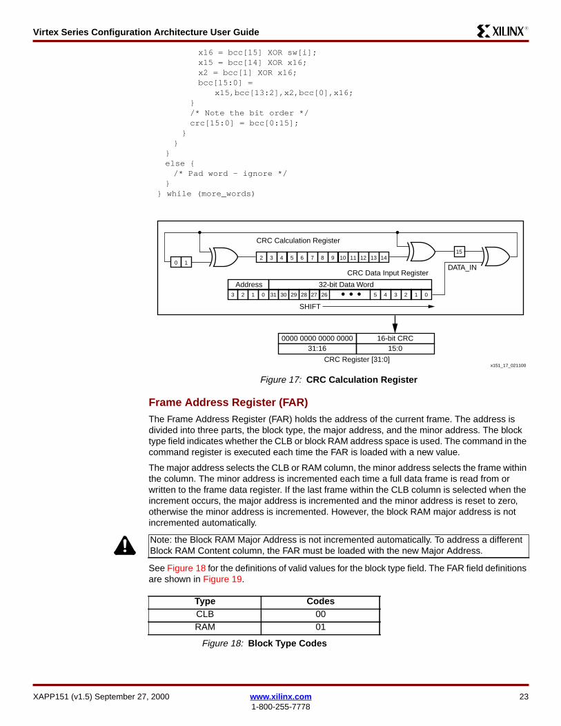
Virtex Series Configuration Architecture User GuideR13
x16 = bcc[15] XOR sw[i]x15 = bcc[14] XOR x16x2 = bcc[1] XOR x16bcc[150] =
x15bcc[132]x2bcc[0]x16 Note the bit order crc[150] = bcc[015]
else
Pad word - ignore
while (more_words)
Frame Address Register (FAR)The Frame Address Register (FAR) holds the address of the current frame The address isdivided into three parts the block type the major address and the minor address The blocktype field indicates whether the CLB or block RAM address space is used The command in thecommand register is executed each time the FAR is loaded with a new value
The major address selects the CLB or RAM column the minor address selects the frame withinthe column The minor address is incremented each time a full data frame is read from orwritten to the frame data register If the last frame within the CLB column is selected when theincrement occurs the major address is incremented and the minor address is reset to zerootherwise the minor address is incremented However the block RAM major address is notincremented automatically
See Figure 18 for the definitions of valid values for the block type field The FAR field definitionsare shown in Figure 19
Figure 17 CRC Calculation Register
Note the Block RAM Major Address is not incremented automatically To address a differentBlock RAM Content column the FAR must be loaded with the new Major Address
Type CodesCLB 00RAM 01
Figure 18 Block Type Codes
x151_17_021100
15141312111098765432
1013
01234526272829303101
Address 32-bit Data Word
CRC Calculation Register
CRC Data Input Register
CRC Register [310]
DATA_IN
SHIFT
23
16-bit CRC13150
0000 0000 0000 0000133116
1313
XAPP151 (v15) September 27 2000 wwwxilinxcom 231-800-255-7778
Virtex Series Configuration Architecture User GuideR13
Frame Data Input Register (FDRI)The Frame Data Input Register (FDRI) is used to load configuration frame data into a Virtexdevice
The Frame Data Register (FDR) is a shift register into which data is loaded prior to transfer tothe configuration memory Configuration data is written to the Virtex device by loading thecommand register with the WCFG command and then loading the FDR with at least two framesof 32-bit words
The write operation is pipelined such that the first frame of data is written to the configurationmemory while the second frame is being shifted in The last frame (the pad frame) is alwaysdummy data which is not actually written to the configuration memory Each frame write mustinclude enough 32 bit data words to load the frame fully There is one pad word at the end ofeach frame which is required for the pipelining hardware
Frame Data Output Register (FDRO)The Frame Data Output Register (FDRO) is for reading configuration data or captured datafrom the Virtex device a process called readback Readback is performed by loading thecommand register with the RCFG command and then addressing the FDRO with a readcommand
Frame Length Register (FLR)Near the beginning of the configuration bitstream the Frame Length Register (FLR) is writtenwith the length of a frame as measured in 32-bit words This length count is used to providesequencing information for the configuration read and write operations Note that the FLR mustbe written before any FDR operation works It is not necessary to set the FLR more than onceIf the number of bits in a frame is not evenly divisible by 32 the length count of the frame mustbe rounded up to the next highest integer The values for the FLR for all the current Virtexseries devices are given in Table 24
BlockType
Major Address(Column Address)
Minor Address(Frame Address)
31 30 29 28 27 26 25 24 23 22 21 20 19 18 17 16 15 14 13 12 11 10 9 8 7 6 5 4 3 2 1 00 0 0 0 0 x x x x x x x x x x x x x x x x x x 0 0 0 0 0 0 0 0 0
Notes1 Locations within fields containing a zero or one must have these values An X in a bit field indicates that the value is variable and must
be set2 Heavy vertical lines are used to separate fields Light vertical lines separate nibbles in the word
Figure 19 Frame Address Fields (FAR)
Note The FLR contains a value that is one less than the number of words that are read fromor written to a given frame This is because the extra word needed for pipelining is not counted
Table 24 Frame Length Register Value
Device Row times Col Frame Length Words per Frame FLR Value
XCV50E 16 times 24 384 12 11
XCV100E 20 times 30 448 14 13
XCV150 24 times 36 512 16 15
XCV200E 28 times 42 576 18 17
XCV300E 32 times 48 672 21 20
24 wwwxilinxcom XAPP151 (v15) September 27 20001-800-255-7778
Virtex Series Configuration Architecture User GuideR13
Legacy Output Register (LOUT)The Legacy Output Register (LOUT) is used for daisy chaining the configuration bitstream toother Xilinx devices Data written to the LOUT is serialized and appears on the DOUT pin
Mask Register (MASK)The Mask Register (MASK) is a mask register for writes to the CTL register A 1 in bit N of themask allows that bit position to be written in the CTL register The default value of the mask isall 0s
Status Register (STAT)The Status Register (STAT) is loaded with current values of several control or status signalsThe register can be read via the re-configuration block or via JTAG The fields in the Statusregister are illustrated in Figure 20 The values of the signals given in Table 25 on page 26 canbe read from the status register
XCV400E 40 times 60 800 25 24
XCV405E 40 times 60 800 25 24
XCV600E 48 times 72 960 30 29
XCV800 56 times 84 1088 34 33
XCV812E 56 times 84 1088 34 33
XCV1000E 64 times 96 1248 39 38
XCV1600E 72 times 108 1376 43 42
XCV2000E 80 times 120 1536 48 47
XCV2600E 92 times 138 1728 54 53
XCV3200E 104 times 156 1952 61 60
Table 24 Frame Length Register Value (Continued)
Device Row times Col Frame Length Words per Frame FLR Value
DO
NE
INIT
MO
DE
GH
IGH
_B
GS
R_B
GW
E_B
GT
S_C
FG
IN_E
RR
OR
LOC
K
CR
C_E
RR
OR
31 30 29 28 27 26 25 24 23 22 21 20 19 18 17 16 15 14 13 12 11 10 9 8 7 6 5 4 3 2 1 00 0 0 0 0 0 0 0 0 0 0 0 0 0 0 0 0 x x x x x x x x x x x x x x x
Notes1 An X in a bit field indicates that the value is variable2 Heavy vertical lines are used to separate fields Light vertical lines separate nibbles in the word
Figure 20 Status Register Fields
XAPP151 (v15) September 27 2000 wwwxilinxcom 251-800-255-7778
Virtex Series Configuration Architecture User GuideR13
ConfigurationInterface
There are two configuration interfaces to the Virtex devices mdash the bit-serial Boundary Scaninterface and the 8-bit byte-serial SelectMAP interface Conceptually XCV50 configurationdata appears as in Figure 21
Frames and words within frames are written in the same order in both configuration interfacesstarting with Frame 0 word 0 (the left-most in the picture) followed by word 1 etc Bits withineach word are written from left to right (MSB first) in the bit-serial configuration interfaces
Within the SelectMAP interface data is written a byte at a time A sample word is shown inFigure 22 The top row indicates the device pin names The bottom row indicates the bit indiceswithin a configuration word Byte 0 loads first followed by byte 1 et cetera The MSB of eachbyte (ie bits 31 23 15 and 7) is loaded on pin D0 The LSB of each byte (ie bits 24 16 8and 0) is loaded on pin D7
PartialReconfigurationof CLBs
Partial reconfiguration can be performed with and without shutting down the device Ifcontention occurs it is advised to go through a shutdown sequence prior to loadingconfiguration frames When shutting down the DONE pin will go active and pull low If this is notdesireable the DONE pin can be prevented from going low by selecting the DONE_CYCLE toKeep State (111) Similarly to prevent GSR from becoming active and reseting the currentstate the GSR_CYCLE can be set to Keep State When not shutting down changes occurframe by frame but is completely done by the end of the Last Frame packet (see Example 1)
Table 25 Status Register Bits
Name Bit Indices Description
DONE 14 Input from DONE pin
INIT 13 Value of INIT
MODE 1210 Value of M2 M1 M0 mode pins
GHIGH_B 9 0 = GHIGH_B asserted
GSR_B 8 0 = all flip-flops are ResetSet
GWE_B 7 1 = flip-flops and block RAM are write disabled
GTS_CFG 6 0 = IOs are tri-stated
IN_ERROR 5 Legacy input error
LOCK 41 Output from DLL lock signals 1 = DLL is locked
CRC_ERROR 0 Indicates that a CRC error has occurred
Data Frame 0 (11 words) Pad Word
hellip
Data Frame n (11 words) Pad WordPad Frame (12 words)
Figure 21 XCV50 Frame Padding for Reads
Figure 22 SelectMAP Byte and Bit Ordering
x151_22_021100
D0 D1 D2 D3 D4 D5 D6 D7 D0 D1 D2 D3 D4 D5 D6 D7 D0 D1 D2 D3 D4 D5 D6 D7 D0 D1 D2 D3 D4 D5 D6 D7
Byte 0 Byte 1 Byte 2 Byte 313
26 wwwxilinxcom XAPP151 (v15) September 27 20001-800-255-7778
Virtex Series Configuration Architecture User GuideR13
The DONE pin will not change in this case Figure 23 illustrates a typical shutdownreconfiguration in the CLB address space and restart sequence
Examples Several examples of reading and evaluating configuration data are provided to illustrate thefollowing
Figure 23 Typical Shutdown Reconfiguration in the CLB Address Spaceand Restart Sequence
FFFF FFFF Dummy WordAA99 5566 Sync Word Does not realign an already synchronized SelectMap port3001 2001 COR0080 FF2F Shutdown bit set optionally set bit 29 DRIVE_DONE
Alternately COR may be read bit 15 set and written back3000 8001 CMD0000 0005 Start Shutdown3000 8001 CMD0000 0007 Reset CRC0000 00000000 0000 Clock shutdown sequence0000 00000000 00003000 8001 CMD0000 0008 Assert GHIGH3000 8001 CMD0000 0001 Write Configuration3000 2001 FAR0--- ---- Block Type CLB (00) MajorMinor Address3000 4--- FDRI + Word Count if count is lt1024 Otherwise use TypeII Header
Write FRAME DATAIf CLB Frames are not written to non-consecutive addresses repeat FAR word followedby new MajorMinor Address followed by FDRI + Word Count and then Frame Data
3000 0001 Write CRC---- ---- CRC3000 8001 CMD0000 0003 LFRM3000 4--- FDRI + Word Count
Write PAD FRAME
3001 2001 COR0080 3F2D Default COR Options
Alternately COR may be read bit 15 cleared and written back3000 8001 CMD0000 0005 Begin Startup3000 0001 Write CRC---- ---- CRC
0000 00000000 0000 4 Dummy Words0000 00000000 0000
Example 1 Read and Write Semaphores in an XCV100 at CLB R1 C1 Slice 0 on page 28Example 2 Reading the Complete Configuration from an XCV50 on page 33
XAPP151 (v15) September 27 2000 wwwxilinxcom 271-800-255-7778
Virtex Series Configuration Architecture User GuideR13
Example 1 Read and Write Semaphores in an XCV100 at CLB R1 C1Slice 0Semaphores are a useful communication mechanism documented in XAPP 153 ldquoStatus andControl Semaphore Registers using Partial Reconfigurationrdquo Figure 24 shows an abstractionof a microprocessor writing control information to an FPGA and reading status informationOne convention for implementing semaphores in Virtex devices is to use two bits of a 16-bitdual-port RAM as illustrated in Figure 25 This occupies one CLB slice with the F-LUTimplementing the control semaphore and the status semaphore implemented in the G-LUTAddress 15 of the G-LUT is used for on-chip writes to the semaphore and address 14 of the F-LUT is used for on-chip reads Conversely the off-chip microprocessor is reading the G-LUT[15] and writing F-LUT[14]
Example 3 Read the Slice 0 G-LUT from CLB R1 C1 from the Complete Configuration of anXCV50 on page 34Example 4 Read the Slice 1 F-LUT from CLB R19 C16 from an XCV100 on page 36Example 5 Read All Bits in Slice 0 G-LUTs from CLB C2 and XCV50 on page 39Example 6 Read Block SelectRAM index 387 of RAM R2 C0 from an XCV100E on page 41
Figure 24 Semaphore Abstraction
x151_ 23_021400
Status13
Control13
MicroProcessor FPGA13
Semaphores13
28 wwwxilinxcom XAPP151 (v15) September 27 20001-800-255-7778
Virtex Series Configuration Architecture User GuideR13
Using a Semaphore Abstraction dual-port RAM ensures that the LUT SelectRAMs are placedin the CLB in a predictable manner When writing data to one or more LUT SelectRAMs or flip-flops on the device all bits in the frame must have valid configuration information This isassured by altering valid configurations from bitstream files or from frames read from a properlyconfigured Virtex device The latter approach is used in this example
Figure 25 Semaphore ReadWrite Implementation
Frame 47
15
14
47 46
47 46
x151_ 24_021100
Select Map
Frame 46
DING
F
13
D2D3D4 5D6 7D0D1 D D
1
111
0
111
Chip Interface
G F
13
XAPP151 (v15) September 27 2000 wwwxilinxcom 291-800-255-7778
Virtex Series Configuration Architecture User GuideR13
Attributes for this design are summarized in Table 26
From the equations in Table 7 on page 11 the values shown in Table 27 can be calculated
From off-chip for reading the G-LUT[15] bit read one frame (MNA=47) For writing the F-LUT[14] bit we show how to read then write one frame (MNA=46) as opposed to modifyingdata from a bitstream file (both are valid methods) The frames on the XCV100 contain 13 32-bit words and one pad word Remember that fm_st_wd is calculated assuming the entireconfiguration has been read However only the pad frame and then frames 46 and 47 fromMajor Address 30 are being read The desired bit is in Frame 1 word 1 which is word 15
The commands for reading both frames (and the pad frame) are given in Figure 26
Table 26 Design Attributes for Example 1
Attribute
G-LUT [15] F-LUT [14]
Read Read Write
Chip_Rows 20
Chip_Cols 30
FL 14
CLB_Row 1
CLB_Col 1
Slice 0
FG 1 0
lut_bit 15 14
RW 1 1 0
Table 27 Semaphore Example Variables Equations and Values
Variable Equation
Value(s)
G-LUT[15] F-LUT[14]
Read Read Write
MJA 1 le 302 rArr 30 ndash 1 times 2 + 2 30
MNA lut_bit + 32ndash 0 times () 47 46
fm_bit_idx 3 + 18 times 1 ndash FG + RW times 32 52 53 21
fm_st_wd 14 times (8 + (30 ndash 1) times 48+ 4647) +RW times (14 +1)= 14 times (1400 + 4647) + 14 times RW= 19600 + 14 times 4647 + 14 times RW
20272 20258 20244
fm_wd floor (2032) 1 1 0
fm_wd_bit_idx 31 + 32 times 110 ndash 525321 11 10 10
30 wwwxilinxcom XAPP151 (v15) September 27 20001-800-255-7778
Virtex Series Configuration Architecture User GuideR13
The 42 words read are shown in Figure 27 F-LUT[14] is in the second frame (frame=1word=1) at bit 10 The value read is a 1 but because the LUT bits are inverted the logic valueis zero G-LUT[15] is in word one of the third data frame (frame=2 word=1) at bit 11The valueread is a 1 which is a logic zero
InstructionData
Hex 31 30 29 28 27 26 25 24 23 22 21 20 19 18 17 16 15 14 13 12 11 10 9 8 7 6 5 4 3 2 1 0
Sync Word AA99 5566 1 0 1 0 1 0 1 0 1 0 0 1 1 0 0 1 0 1 0 1 0 1 0 1 0 1 1 0 0 1 1 0
Write next (1) word to FAR 3000 2001 0 0 1 1 0 0 0 0 0 0 0 0 0 0 0 0 0 0 1 0 0 0 0 0 0 0 0 0 0 0 0 1
CLB MJA=30 MNA=46 003C 5800 0 0 0 0 0 0 0 0 0 0 1 1 1 1 0 0 0 1 0 1 1 1 0 0 0 0 0 0 0 0 0 0
Write next word to CMD 3000 8001 0 0 1 1 0 0 0 0 0 0 0 0 0 0 0 0 1 0 0 0 0 0 0 0 0 0 0 0 0 0 0 1
Register value for RCFG 0000 0004 0 0 0 0 0 0 0 0 0 0 0 0 0 0 0 0 0 0 0 0 0 0 0 0 0 0 0 0 0 1 0 0
Read from FDRO 2800 602A 0 0 1 0 1 0 0 0 0 0 0 0 0 0 0 0 0 1 1 0 0 0 0 0 0 0 1 0 1 0 1 0
Flush pipe 0000 0000 0 0 0 0 0 0 0 0 0 0 0 0 0 0 0 0 0 0 0 0 0 0 0 0 0 0 0 0 0 0 0 0
(read 42 words)
Notes1 Binary data is grouped in two ways for ease of interpretation Thin vertical lines separate nibble boundaries Heavy vertical lines
separate field boundaries
Figure 26 Commands to Read Two Data Frames
XAPP151 (v15) September 27 2000 wwwxilinxcom 311-800-255-7778
Virtex Series Configuration Architecture User GuideR13
To write to the F-LUT semaphore start with the second data frame (frame=1) that was justread Words 1 - 13 of that frame will become words 0 - 12 of the frame to be written Word 13of this new frame is a pad word and can have any value (typically 0 is chosen) In this newframe set bit 11 of word 0 (zero) to the desired value of the semaphore A pad frame mustfollow the data frame The commands from Figure 28 write these two frames into the device atthe proper location
Frame Word 31 30 29 28 27 26 25 24 23 22 21 20 19 18 17 16 15 14 13 12 11 10 9 8 7 6 5 4 3 2 1 0
0
0 1 1 1 1 1 1 1 1 1 1 1 1 1 1 1 1 1 1 1 1 1 1 1 1 1 1 1 1 1 1 1 1
1 1 1 1 1 1 1 1 1 1 1 1 1 1 1 1 1 1 1 1 1 1 1 1 1 1 1 1 1 1 1 1 1
2 1 1 1 1 1 1 1 1 1 1 1 1 1 1 1 1 1 1 1 1 1 1 1 1 1 1 1 1 1 1 1 1
3 1 1 1 1 1 1 1 1 1 1 1 1 1 1 1 1 1 1 1 1 1 1 1 1 1 1 1 1 1 1 1 1
4 1 1 1 1 1 1 1 1 1 1 1 1 1 1 1 1 1 1 1 1 1 1 1 1 1 1 1 1 1 1 1 1
5 1 1 1 1 1 1 1 1 1 1 1 1 1 1 1 1 1 1 1 1 1 1 1 1 1 1 1 1 1 1 1 1
6 1 1 1 1 1 1 1 1 1 1 1 1 1 1 1 1 1 1 1 1 1 1 1 1 1 1 1 1 1 1 1 1
7 1 1 1 1 1 1 1 1 1 1 1 1 1 1 1 1 1 1 1 1 1 1 1 1 1 1 1 1 1 1 1 1
8 1 1 1 1 1 1 1 1 1 1 1 1 1 1 1 1 1 1 1 1 1 1 1 1 1 1 1 1 1 1 1 1
9 1 1 1 1 1 1 1 1 1 1 1 1 1 1 1 1 1 1 1 1 1 1 1 1 1 1 1 1 1 1 1 1
10 1 1 1 1 1 1 1 1 1 1 1 1 1 1 1 1 1 1 1 1 1 1 1 1 1 1 1 1 1 1 1 1
11 1 1 1 1 1 1 1 1 1 1 1 1 1 1 1 1 1 1 1 1 1 1 1 1 1 1 1 1 1 1 1 1
12 1 1 1 1 1 1 1 1 1 1 1 1 1 1 1 1 1 1 1 1 1 1 1 1 1 1 1 1 1 1 1 1
13 1 1 1 1 1 1 1 1 1 1 1 1 1 1 1 1 1 1 1 1 1 1 1 1 1 1 1 1 1 1 1 1
1
0 0 0 0 0 0 0 0 0 0 0 0 0 0 0 0 0 0 0 0 0 0 0 0 0 0 0 0 0 0 0 0 0
1 1 0 0 0 0 0 0 0 0 0 0 0 1 0 0 0 0 1 1 0 1 1 0 0 0 0 0 0 0 0 0 0 F[14]
2 1 1 1 1 1 0 1 1 0 0 0 0 1 1 1 1 0 0 1 1 1 1 1 0 1 1 0 0 0 0 0 0
3 0 0 0 0 1 1 1 1 1 0 1 1 0 0 0 0 0 0 0 0 0 0 1 1 1 1 1 0 1 1 0 0
4 0 0 0 0 0 0 0 0 1 1 1 1 0 0 0 0 0 0 0 0 0 0 0 0 0 0 1 1 1 1 1 0
5 1 1 0 0 1 1 0 0 0 0 0 0 1 1 0 0 1 0 1 1 0 0 0 0 0 0 0 0 0 0 1 1
6 1 1 1 0 1 1 0 0 0 0 0 0 1 1 1 0 1 1 1 0 1 0 1 1 0 0 0 0 0 0 0 0
7 0 0 1 1 1 1 1 0 1 1 0 0 0 0 1 1 0 0 0 0 1 1 1 1 1 0 1 1 0 0 0 0
8 0 0 0 0 0 0 1 1 1 1 1 0 0 0 0 0 0 0 0 0 0 0 0 0 1 1 1 1 1 0 1 1
9 0 0 0 0 0 0 0 0 0 0 1 1 0 0 0 0 1 1 0 0 0 0 0 0 0 0 0 0 1 1 1 1
10 1 0 1 1 0 0 0 0 0 0 0 0 1 0 1 1 1 1 1 0 1 1 0 0 0 0 0 0 0 0 0 0
11 1 1 1 1 1 0 1 1 0 0 0 0 1 1 1 1 0 0 1 1 1 1 1 0 1 1 0 0 0 0 0 0
12 0 0 0 0 1 1 0 1 1 0 1 1 0 0 0 0 0 0 0 0 0 0 1 1 1 1 1 0 0 0 0 0
13 0 0 0 0 0 0 1 1 0 1 0 1 0 0 0 0 0 0 0 0 0 0 0 0 0 0 0 0 0 0 0 0
2
0 0 0 0 0 0 0 0 0 0 0 0 0 0 0 0 0 0 0 0 0 0 0 0 0 0 0 0 0 0 0 0 0
1 1 0 1 0 0 0 0 0 0 0 0 1 1 0 1 0 1 1 1 0 1 1 0 0 0 0 0 0 0 0 0 0 G[15]
2 1 1 1 1 1 1 1 1 0 0 0 0 1 1 1 1 0 0 1 1 1 1 1 1 1 1 0 0 0 0 0 0
3 0 0 0 0 1 1 1 1 1 1 1 1 0 0 0 0 0 0 0 0 0 0 1 0 1 1 1 1 1 1 0 0
4 0 0 0 0 0 0 0 0 1 1 1 1 0 0 0 0 0 0 0 0 0 0 0 0 0 0 1 1 1 1 1 1
5 1 1 0 0 0 0 0 0 0 0 0 0 1 1 0 0 1 1 1 1 0 0 1 0 0 0 0 0 0 0 1 1
6 1 1 1 1 1 1 0 0 0 0 0 0 1 1 1 1 1 1 1 1 1 1 1 1 0 0 0 0 0 0 0 0
7 0 0 1 1 1 1 1 1 1 1 0 0 0 0 1 1 0 0 0 0 1 1 1 1 1 1 1 1 0 0 0 0
8 0 0 0 0 0 0 1 1 1 1 1 1 0 0 0 0 0 0 0 0 0 0 0 0 1 1 1 1 1 1 1 1
9 0 0 0 0 0 0 0 0 0 0 1 1 0 0 0 0 1 1 0 0 0 0 0 0 0 0 0 0 1 1 1 1
10 1 1 1 1 0 0 0 0 0 0 0 0 1 1 1 1 1 1 1 1 1 1 0 0 0 0 0 0 0 0 0 0
11 1 1 1 1 1 1 1 1 0 0 0 0 1 1 1 1 0 0 1 1 1 1 1 1 1 1 0 0 0 0 0 0
12 0 0 0 0 1 1 0 1 1 1 1 1 0 0 0 0 0 0 0 0 0 0 1 1 1 1 1 0 1 0 0 0
13 0 0 0 0 0 1 1 0 0 1 1 1 0 0 0 0 0 0 0 0 0 0 0 0 0 0 0 0 0 0 0 0
Figure 27 Three Frames Containing the Semaphores
32 wwwxilinxcom XAPP151 (v15) September 27 20001-800-255-7778
Virtex Series Configuration Architecture User GuideR13
Example 2 Reading the Complete Configuration from an XCV50Steps
1 If flip-flop values are needed clock the on-chip signal CAPTURE to capture flip-flopvalues See the Xilinx Libraries Guide for use of the CAPTURE_VIRTEX cell
2 Write the starting frame address (CLB MJA=0 MNA=0) into the FAR
3 Write the RCFG command to the CMD register
4 Address the FDRO register with a READ operation and word count equal to the number of32-bit words in the CLB frames plus one pad frame
5 Read the data following the timing diagrams in the SelectMAP interface section
6 Write the address for RAM block 0 to the FAR
7 Address the FDRO register with a read operation and word count equal to the number of32-bit words in the RAM block plus one pad frame
8 Read the data
9 Write the address for RAM block 1 to the FAR
10 Address the FDRO register with a read operation and word count equal to the number of32-bit words in the RAM block plus one pad frame
11 Read the data
When using SelectMAP mode to read data words from the Virtex device de-assert CS de-assert WRITE assert CS then clock the data out When using JTAG load the JTAG IR
InstructionData
Hex 31 30 29 28 27 26 25 24 23 22 21 20 19 18 17 16 15 14 13 12 11 10 9 8 7 6 5 4 3 2 1 0
Sync Word AA995566
1 0 1 0 1 0 1 0 1 0 0 1 1 0 0 1 0 1 0 1 0 1 0 1 0 1 1 0 0 1 1 0
Write next (1) word to FAR 30002001
0 0 1 1 0 0 0 0 0 0 0 0 0 0 0 0 0 0 1 0 0 0 0 0 0 0 0 0 0 0 0 1
MJA=30 MNA=46 003C5C00
0 0 0 0 0 0 0 0 0 0 1 1 1 1 0 0 0 1 0 1 1 1 0 0 0 0 0 0 0 0 0 0
Write next word to CMD 30008001
0 0 1 1 0 0 0 0 0 0 0 0 0 0 0 0 1 0 0 0 0 0 0 0 0 0 0 0 0 0 0 1
Register value for WCFG 00000001
0 0 0 0 0 0 0 0 0 0 0 0 0 0 0 0 0 0 0 0 0 0 0 0 0 0 0 0 0 0 0 1
Write 28 words to FDRI 3000401C
0 0 1 1 0 0 0 0 0 0 0 0 0 0 0 0 0 1 0 0 0 0 0 0 0 0 0 1 1 1 0 0
Data Word 0 A01AEC00
1 0 1 0 0 0 0 0 0 0 0 1 1 0 1 0 1 1 1 0 1 1 0 0 0 0 0 0 0 0 0 0
Data Word 1 FF0F3FC0
1 1 1 1 1 1 1 1 0 0 0 0 1 1 1 1 0 0 1 1 1 1 1 1 1 1 0 0 0 0 0 0
Data Word 2 0FF002FC
0 0 0 0 1 1 1 1 1 1 1 1 0 0 0 0 0 0 0 0 0 0 1 0 1 1 1 1 1 1 0 0
hellip hellip hellip
Data Word 27 00000000
0 0 0 0 0 0 0 0 0 0 0 0 0 0 0 0 0 0 0 0 0 0 0 0 0 0 0 0 0 0 0 0
Notes1 Binary data is grouped in two ways for ease of interpretation Thin vertical lines separate nibble boundaries Heavy
vertical lines separate field boundaries
Figure 28 Commands to Write a Semaphore Value
XAPP151 (v15) September 27 2000 wwwxilinxcom 331-800-255-7778
Virtex Series Configuration Architecture User GuideR13
(instruction register) with the CFG_OUT instruction Then go to the SDR (Shift-DR) state andshift the data out (See Figure 29)
Example 3 Read the Slice 0 G-LUT from CLB R1 C1 from the CompleteConfiguration of an XCV50The commands for reading the bitstream from the Virtex device are given in Example 1 Readand Write Semaphores in an XCV100 at CLB R1 C1 Slice 0 on page 28 Using an XCV50device the independent attributes are show in Table 28
InstructionData
Hex 31 30 29 28 27 26 25 24 23 22 21 20 19 18 17 16 15 14 13 12 11 10 9 8 7 6 5 4 3 2 1 0
Sync Word AA99 5566 1 0 1 0 1 0 1 0 1 0 0 1 1 0 0 1 0 1 0 1 0 1 0 1 0 1 1 0 0 1 1 0
Write next word to FAR 3000 2001 0 0 1 1 0 0 0 0 0 0 0 0 0 0 0 0 0 0 1 0 0 0 0 0 0 0 0 0 0 0 0 1
CLB MJA=0 MNA=0 0000 0000 0 0 0 0 0 0 0 0 0 0 0 0 0 0 0 0 0 0 0 0 0 0 0 0 0 0 0 0 0 0 0 0
Write next word to CMDregister
3000 8001 0 0 1 1 0 0 0 0 0 0 0 0 0 0 0 0 1 0 0 0 0 0 0 0 0 0 0 0 0 0 0 1
Register value for RCFG 0000 0004 0 0 0 0 0 0 0 0 0 0 0 0 0 0 0 0 0 0 0 0 0 0 0 0 0 0 0 0 0 1 0 0
Read from FDRO register 2800 6000 0 0 1 0 1 0 0 0 0 0 0 0 0 0 0 0 0 1 1 0 0 0 0 0 0 0 0 0 0 0 0 0
15876 words 4800 3E04 0 1 0 0 1 0 0 0 0 0 0 0 0 0 0 0 0 0 1 1 1 1 1 0 0 0 0 0 0 1 0 0
Flush pipe 0000 0000 0 0 0 0 0 0 0 0 0 0 0 0 0 0 0 0 0 0 0 0 0 0 0 0 0 0 0 0 0 0 0 0
(Read 15876 words)Write to FAR register 3000 2001 0 0 1 1 0 0 0 0 0 0 0 0 0 0 0 0 0 0 1 0 0 0 0 0 0 0 0 0 0 0 0 1
RAM MJA=0 MNA=0 0200 0000 0 0 0 0 0 0 1 0 0 0 0 0 0 0 0 0 0 0 0 0 0 0 0 0 0 0 0 0 0 0 0 0
Read 780 words fromFDRO reg
2800 630C 0 0 1 0 1 0 0 0 0 0 0 0 0 0 0 0 0 1 1 0 0 0 1 1 0 0 0 0 1 1 0 0
Flush pipe 0000 0000 0 0 0 0 0 0 0 0 0 0 0 0 0 0 0 0 0 0 0 0 0 0 0 0 0 0 0 0 0 0 0 0
(Read 780 words)Write to FAR register 3000 2001 0 0 1 1 0 0 0 0 0 0 0 0 0 0 0 0 0 0 1 0 0 0 0 0 0 0 0 0 0 0 0 1
RAM MJA=1 MNA=0 0202 0000 0 0 0 0 0 0 1 0 0 0 0 0 0 0 1 0 0 0 0 0 0 0 0 0 0 0 0 0 0 0 0 0
Read 780 words fromFDRO reg
2800 630C 0 0 1 0 1 0 0 0 0 0 0 0 0 0 0 0 0 1 1 0 0 0 1 1 0 0 0 0 1 1 0 0
Flush pipe 0000 0000 0 0 0 0 0 0 0 0 0 0 0 0 0 0 0 0 0 0 0 0 0 0 0 0 0 0 0 0 0 0 0 0
(Read 780 words)
Figure 29 Example 2 - Read Complete Configuration for XCV50
Table 28 XCV50 Independent Attributes
Independent Attributes Values
Chip_Rows 16
Chip_Cols 24
FL 12
CLB_Row 1
CLB_Col 1
FG 1
Slice 0
RW 1
34 wwwxilinxcom XAPP151 (v15) September 27 20001-800-255-7778
Virtex Series Configuration Architecture User GuideR13
From the equations given earlier in Table 7 calculating the range of values for fm_st_wdindicates that the word 13740 of the configuration is the starting word of the 12-word (FL=12)frame containing bit 0 of the G-LUT in Slice 0 of CLB R1C1 (Table 29)
The configuration bits for the given frame are as follows G-LUT[0] is in fm_wd=0 at bit 11
All 16 LUT SelectRAM bits are in the following words at the same bit index 11
Table 29 Variables Equations and Values for Slice 0 G-LUT
Variables Equations Values
MJA 1 le 242 rArr 24 ndash 1times 2 + 2 24
MNA 0 times (hellip) + lut_bit + 32 0 321 332 343 35
4 365 376 387 39
8 409 41
10 4211 43
12 4413 4514 4615 47
fm_bit_idx 3 + 18 times 1 ndash1 + RW times 32 52
fm_st_wd 12 times (8+ (24 ndash1) times 48 + [3247]) +1 x 12= 12 times (1112 + [3247]) +12= 13356 + 12 times 3247]
1374013920
fm_wd floor(5232) 1
fm_wd_bit_idx 31 + 32 ndash 52 11
BitstreamWord
Frame 32-bit Word FrameWord31 30 29 28 27 26 25 24 23 22 21 20 19 18 17 16 15 14 13 12 11 10 9 8 7 6 5 4 3 2 1 0
13740 0 0 0 0 0 0 0 0 0 0 0 0 0 0 0 0 0 0 0 0 0 0 0 0 0 0 0 0 0 0 0 0 013741 0 0 1 0 1 0 0 0 0 0 0 0 0 1 0 1 0 1 0 0 1 1 1 0 0 0 0 0 0 0 0 0 113742 1 0 1 1 0 0 1 1 0 0 0 0 0 0 0 0 0 0 1 0 1 1 0 0 1 1 0 0 0 0 0 0 213743 0 0 0 0 1 0 1 1 0 0 1 1 0 0 0 0 0 0 0 0 0 0 1 0 1 1 0 0 1 1 0 0 313744 0 0 0 0 0 0 0 0 1 0 1 1 0 0 1 1 0 0 0 0 0 0 0 0 0 0 1 0 1 1 0 0 413745 1 1 0 0 0 0 0 0 0 0 0 0 1 0 1 1 0 0 1 1 0 0 0 0 0 0 0 0 0 0 1 0 513746 1 1 0 0 1 1 0 0 0 0 0 0 0 0 0 0 1 0 1 1 0 0 1 1 0 0 0 0 0 0 0 0 613747 0 0 1 0 1 1 0 0 1 1 0 0 0 0 0 0 0 0 0 0 1 0 1 1 0 0 1 1 0 0 0 0 713748 0 0 0 0 0 0 1 0 1 1 0 0 1 1 0 0 0 0 0 0 0 0 0 0 1 0 1 1 0 0 1 1 813749 0 0 0 0 0 0 0 0 0 0 1 0 1 1 0 0 1 1 0 0 0 0 0 0 0 0 0 0 1 0 1 1 913750 0 0 1 1 0 0 0 0 0 0 0 0 0 0 1 0 1 1 0 0 1 0 1 0 0 0 0 0 0 0 0 0 1013751 0 1 0 1 0 0 0 0 0 0 0 0 0 0 0 0 0 0 0 0 0 0 0 0 0 0 0 0 0 0 0 0 11
Figure 30 Configuration Bits for Slice 0 CLB R1C1 G-LUT [0]
XAPP151 (v15) September 27 2000 wwwxilinxcom 351-800-255-7778
Virtex Series Configuration Architecture User GuideR13
The 16 bits are LUT[150]=0111111111111111 The LUT SelectRAM bits are inverted from theirlogic values The ldquologicalrdquo contents are LUT[150]=1000000000000000 Thus this G-LUTimplements a 4-input AND function
Example 4 Read the Slice 1 F-LUT from CLB R19 C16 from an XCV100Commands for reading the bitstream from the Virtex device are given in Figure 32 Use thefollowing independent attributes to find the given F-LUT
From the equations in Table 7 on page 11 calculating fm_st_wd indicates the starting wordwith respect to a configuration that starts at MJA=0 MNA=0 Because the frames we are
BitstreamWord
Frame 32-bit Word
LUT Bit31 30 29 28 27 26 25 24 23 22 21 20 19 18 17 16 15 14 13 12 11 10 9 8 7 6 5 4 3 2 1 0
13741 0 0 1 0 1 0 0 0 0 0 0 0 0 1 0 1 0 1 0 0 1 1 1 0 0 0 0 0 0 0 0 0 0
13753 1 0 1 0 0 0 0 0 0 0 0 0 0 0 0 1 0 0 0 1 1 1 0 0 0 0 0 0 0 0 0 0 1
13765 1 0 1 0 1 0 0 0 0 0 0 0 1 0 0 0 0 0 0 1 1 1 1 0 0 0 0 0 0 0 0 0 2
13777 0 0 0 0 1 0 0 0 0 0 0 1 1 1 0 1 1 0 1 0 1 1 0 0 0 0 0 0 0 0 0 0 3
13789 0 1 0 0 0 0 0 0 0 0 0 0 0 1 0 1 1 1 1 1 1 1 1 0 0 0 0 0 0 0 0 0 4
13801 1 0 1 0 1 0 0 0 0 0 0 1 0 0 0 1 1 0 0 1 1 1 0 0 0 0 0 0 0 0 0 0 5
13813 0 0 0 1 0 0 0 0 0 0 0 0 0 0 0 0 1 0 0 1 1 1 0 0 0 0 0 0 0 0 0 0 6
13825 0 1 1 0 1 0 0 0 0 0 0 1 0 1 0 0 1 1 0 0 1 1 0 0 0 0 0 0 0 0 0 0 7
13837 1 0 1 1 1 0 0 0 0 0 0 1 0 1 0 1 1 0 0 0 1 1 0 0 0 0 0 0 0 0 0 0 8
13849 1 0 0 0 0 0 0 0 0 0 0 0 0 0 0 0 1 1 1 0 1 1 0 0 0 0 0 0 0 0 0 0 9
13861 1 0 0 0 0 0 0 0 0 0 0 1 0 0 0 0 1 1 1 1 1 1 1 0 0 0 0 0 0 0 0 0 10
13873 1 0 0 0 0 0 0 1 0 0 0 0 0 1 0 0 0 1 1 0 1 1 0 0 0 1 0 0 0 0 0 0 11
13885 1 0 0 0 0 0 0 0 0 0 0 0 0 1 0 1 0 0 1 0 1 1 0 0 0 0 0 0 0 0 0 0 12
13897 0 0 0 0 1 0 0 0 0 0 0 0 0 1 0 0 0 0 0 0 1 1 0 0 0 0 0 0 0 0 0 0 13
13909 1 0 0 0 0 0 0 0 0 0 0 0 1 1 0 1 0 1 1 0 1 1 0 0 0 0 0 0 0 0 0 0 14
13921 1 0 1 0 0 0 0 0 0 0 0 1 1 1 0 1 1 1 1 1 0 1 0 0 0 0 0 0 0 0 0 0 15
Figure 31 Location of all 16 LUT SelectRAM Bits
Table 30 Virtex Bitstream Command Attributes
Independent Attributes Values
Chip_Rows 20
Chip_Cols 30
FL 14
CLB_Row 19
CLB_Col 16
FG 0
Slice 1
RW 1
36 wwwxilinxcom XAPP151 (v15) September 27 20001-800-255-7778
Virtex Series Configuration Architecture User GuideR13
interested in start at MJA=1 MNA=0 which is fm_st_wd = 126 so the first 126 words are notneeded (0ndash125) Therefore to find the given Slice 1 F-LUT see Table 31
Sixteen frames need to be read one for each bit in the LUT SelectRAM The bits in LUTSelectRAMs in Slice 1 occur in the opposite order that they do for Slice 0 LUT SelectRAMs
Frames are read sequentially with ascending addresses If read in LUT bit order LUT[0]LUT[1] hellip LUT[15] These are stored in descending addresses which require 16 separateread operations each reading one data frame and one pad frame However if read inascending address order LUT[15] LUT[14] hellip LUT[0] all 16 data frames are read with asingle read operation This requires only one pad frame for all 16 frames Thus it takes lesstime to read ascending frames starting at MJA=1 MNA=0 and finishing with frame MJA=1MNA=15 The frames in the XCV100 contain 14 32-bit words and a single pad wordCommands for reading only the F-LUT data are given in Figure 32
Table 31 Variables Equations and Values for Slice 1 F-LUT
Variables Equations Values
MJA 16 gt 302 rArr 2times16 ndash 30 ndash1 1
MNA lut_bit + 32 ndash Slice times (2 times lut_bit +17)= [015] + 32 ndash (2 times [015] + 17)= 15 ndash [015]
0 151 142 133 12
4 115 106 97 8
8 79 6
10 511 4
12 313 214 115 0
fm_bit_idx 3 + 18 times 19 ndash 0+ 32 377
fm_st_wd 14 times (8 + (1ndash 1) times 48 + [150]) +1 times 14= 14 times (8 + [150]) +14= 126 + 14 times [150]
= 336126
fm_wd floor(37732) 11
fm_wd_bit_idx 31 + 32 times 11 ndash 377 6
XAPP151 (v15) September 27 2000 wwwxilinxcom 371-800-255-7778
Virtex Series Configuration Architecture User GuideR13
The 377th bit of each frame is the bit in the F-LUT This LUT SelectRAM bit is in the framersquosword index 11 bit index 6
The configuration bits for the given frame in Figure 33 are as follows LUT Bit 15 is in MJA=1MNA=0 fm_wd=11 at bit 6
LUT bit 0 is in MJA=1 MNA=15 fm_wd=11 at bit 6
InstructionData
Hex 31 30 29 28 27 26 25 24 23 22 21 20 19 18 17 16 15 14 13 12 11 10 9 8 7 6 5 4 3 2 1 0
Sync Word AA99 5566 1 0 1 0 1 0 1 0 1 0 0 1 1 0 0 1 0 1 0 1 0 1 0 1 0 1 1 0 0 1 1 0
Write next (1) word to FAR 3000 2001 0 0 1 1 0 0 0 0 0 0 0 0 0 0 0 0 0 0 1 0 0 0 0 0 0 0 0 0 0 0 0 1
CLB MJA = 1 MNA = 0 0002 0000 0 0 0 0 0 0 0 0 0 0 0 0 0 0 1 0 0 0 0 0 0 0 0 0 0 0 0 0 0 0 0 0
Write next word to CMD 3000 8001 0 0 1 1 0 0 0 0 0 0 0 0 0 0 0 0 1 0 0 0 0 0 0 0 0 0 0 0 0 0 0 1
Register value for RCFG 0000 0004 0 0 0 0 0 0 0 0 0 0 0 0 0 0 0 0 0 0 0 0 0 0 0 0 0 0 0 0 0 1 0 0
Read from FDRO 2800 60EE 0 0 1 0 1 0 0 0 0 0 0 0 0 0 0 0 0 1 1 0 0 0 0 0 1 1 1 0 1 1 1 0
Flush pipe 0000 0000 0 0 0 0 0 0 0 0 0 0 0 0 0 0 0 0 0 0 0 0 0 0 0 0 0 0 0 0 0 0 0 0
(Read 238 words)
Figure 32 Commands to read Slice 1 F-LUT
Frame WordFrame 32-bit Word
31 30 29 28 27 26 25 24 23 22 21 20 19 18 17 16 15 14 13 12 11 10 9 8 7 6 5 4 3 2 1 0
0 0 0 0 0 0 0 0 0 0 0 0 0 0 0 0 0 0 0 0 0 0 0 0 0 0 0 0 0 0 0 0 0
1 1 1 0 0 0 0 0 0 0 0 0 0 0 1 0 1 1 1 1 1 1 1 0 0 0 0 0 0 0 0 0 0
2 1 1 1 1 1 1 1 1 0 0 0 0 0 0 0 0 0 0 1 1 1 1 1 1 1 1 0 0 0 0 0 0
3 0 0 0 0 1 1 1 1 1 1 1 1 0 0 0 0 0 0 0 0 0 0 1 1 1 1 1 1 1 1 0 0
4 0 0 0 0 0 0 0 0 1 1 1 1 1 1 1 1 0 0 0 0 0 0 0 0 0 0 1 1 1 1 1 1
5 1 1 0 0 0 0 0 0 0 0 0 0 1 1 1 1 1 1 1 1 0 0 0 0 0 0 0 0 0 0 1 1
6 1 1 1 1 1 1 0 0 0 0 0 0 0 0 0 0 1 1 1 1 1 1 1 1 0 0 0 0 0 0 0 0
7 0 0 1 1 1 1 1 1 1 1 0 0 0 0 0 0 0 0 0 0 1 1 1 1 1 1 1 1 0 0 0 0
8 0 0 0 0 0 0 1 1 1 1 1 1 1 1 0 0 0 0 0 0 0 0 0 0 1 1 1 1 1 1 1 1
9 0 0 0 0 0 0 0 0 0 0 1 1 1 1 1 1 1 1 0 0 0 0 0 0 0 0 0 0 1 1 1 1
10 1 1 1 1 0 0 0 0 0 0 0 0 0 0 1 1 1 1 1 1 1 1 0 0 0 0 0 0 0 0 0 0
11 1 1 1 1 1 1 1 1 0 0 0 0 0 0 0 0 0 0 1 1 1 1 1 1 1 0 0 0 0 0 0 0
12 0 0 0 0 1 1 1 1 1 1 1 1 0 0 0 0 0 0 0 0 0 0 1 1 1 1 1 1 0 0 0 0
13 0 0 0 0 0 0 0 0 0 1 1 1 0 0 0 0 0 0 0 0 0 0 1 1 1 1 1 1 0 0 0 0
Figure 33 Frame Containing F-LUT[15]
Bit streamWord
Frame 32-bit WordFmWd31 30 29 28 27 26 25 24 23 22 21 20 19 18 17 16 15 14 13 12 11 10 9 8 7 6 5 4 3 2 1 0
336 0 0 0 0 0 0 0 0 0 0 0 0 0 0 0 0 0 0 0 0 0 0 0 0 0 0 0 0 0 0 0 0 0337 0 1 0 0 1 0 0 0 0 0 0 1 0 1 0 0 1 1 0 0 1 1 0 0 0 0 0 0 0 0 0 0 1338 1 0 1 1 0 0 1 1 0 0 0 0 0 0 0 0 0 0 1 0 1 1 0 0 1 1 0 0 0 0 0 0 2339 0 0 0 0 1 0 1 1 0 0 1 1 0 0 0 0 0 0 0 0 0 0 1 0 1 1 0 0 1 1 0 0 3340 0 0 0 0 0 0 0 0 1 0 1 1 0 0 1 1 0 0 0 0 0 0 0 0 0 0 1 0 1 1 0 0 4341 1 1 0 0 0 0 0 0 0 0 0 0 1 0 1 1 0 0 1 1 0 0 0 0 0 0 0 0 0 0 1 0 5342 1 1 0 0 1 1 0 0 0 0 0 0 0 0 0 0 1 0 1 1 0 0 1 1 0 0 0 0 0 0 0 0 6343 0 0 1 0 1 1 0 0 1 1 0 0 0 0 0 0 0 0 0 0 1 0 1 1 0 0 1 1 0 0 0 0 7
Figure 34 Frame Containing F-LUT [0]
38 wwwxilinxcom XAPP151 (v15) September 27 20001-800-255-7778
Virtex Series Configuration Architecture User GuideR13
For the sake of brevity here are the sixteen 11th words in the order they appear in thebitstream
The bits are LUT[150]=0111111111111111 The LUT SelectRAM bits are inverted from thelogic sense The logical contents are LUT[150]=1000000000000000 Thus this F-LUTimplements a 4-input AND gate
Example 5 Read All Bits in Slice 0 G-LUTs from CLB C2 and XCV50Given the following attributes the necessary values to find the G-LUT data can be computed
344 0 0 0 0 0 0 1 0 1 1 0 0 1 1 0 0 0 0 0 0 0 0 0 0 1 0 1 1 0 0 1 1 8345 0 0 0 0 0 0 0 0 0 0 1 0 1 1 0 0 1 1 0 0 0 0 0 0 0 0 0 0 1 0 1 1 9346 0 0 1 1 0 0 0 0 0 0 0 0 0 0 1 0 1 1 0 0 1 1 0 0 0 0 0 0 0 0 0 0 10347 1 1 1 1 1 0 1 1 0 0 0 0 0 0 0 0 0 0 1 0 1 1 1 0 1 1 0 1 0 0 0 0 11348 0 0 0 0 1 1 1 0 1 0 1 1 0 0 0 0 0 0 0 0 0 0 1 1 1 1 0 1 0 0 0 0 12349 0 0 0 0 0 1 0 0 0 0 1 0 0 0 0 0 0 0 0 0 0 0 0 0 0 0 0 0 0 0 0 0 13
Bit streamWord
Frame 32-bit WordFmWd31 30 29 28 27 26 25 24 23 22 21 20 19 18 17 16 15 14 13 12 11 10 9 8 7 6 5 4 3 2 1 0
Figure 34 Frame Containing F-LUT [0]
BitstreamWord
Frame 32-bit WordLUT Bit31 30 29 28 27 26 25 24 23 22 21 20 19 18 17 16 15 14 13 12 11 10 9 8 7 6 5 4 3 2 1 0
137 1 1 1 1 1 1 1 1 0 0 0 0 0 0 0 0 0 0 1 1 1 1 1 1 1 0 0 0 0 0 0 0 15151 1 0 1 1 1 0 1 1 0 0 0 0 0 0 0 0 0 0 1 0 1 1 1 0 1 1 0 0 0 0 0 0 14165 1 0 1 1 0 0 1 1 0 0 0 0 0 0 0 0 0 0 1 0 1 1 1 0 1 1 0 0 0 0 0 0 13179 1 0 1 1 1 0 1 1 0 0 0 0 0 0 0 0 0 0 1 0 1 1 1 0 1 1 0 0 0 0 0 0 12193 1 1 1 1 1 0 1 1 0 0 0 0 0 0 0 0 0 0 1 1 1 1 1 0 1 1 0 0 0 0 0 0 11207 1 1 1 1 1 1 1 1 0 0 0 0 0 0 0 0 0 0 1 1 1 1 1 1 1 1 1 0 1 0 0 0 10221 1 1 1 1 1 0 1 1 0 0 0 0 0 0 0 0 0 0 1 1 1 1 1 0 1 1 0 0 0 0 0 0 9235 1 0 1 1 1 0 1 1 0 0 0 0 0 0 0 0 0 0 1 0 1 1 1 0 1 1 0 0 0 0 0 0 8249 1 0 1 1 0 0 1 1 0 0 0 0 0 0 0 0 0 0 1 0 1 1 0 0 1 1 0 0 0 0 0 0 7263 1 0 1 1 0 1 1 1 1 0 0 0 0 0 0 0 0 0 1 0 1 1 0 1 1 1 0 0 0 0 0 0 6277 1 1 1 1 0 0 1 1 0 0 0 0 0 0 0 0 0 0 1 1 1 1 0 0 1 1 0 0 0 0 0 0 5291 1 1 1 1 1 1 1 1 0 0 0 0 0 0 0 0 0 0 1 1 1 1 1 1 1 1 0 0 0 0 0 0 4305 1 1 1 1 1 0 1 1 0 0 0 0 0 0 0 0 0 0 1 1 1 1 1 0 1 1 0 0 0 0 0 0 3319 1 0 1 1 0 1 1 1 0 0 0 0 0 0 0 0 0 0 1 0 1 1 0 1 1 1 0 0 0 0 0 0 2333 1 0 1 1 0 0 1 1 0 0 0 0 0 0 0 0 0 0 1 0 1 1 0 0 1 1 0 0 0 0 0 0 1347 1 1 1 1 1 0 1 1 0 0 0 0 0 0 0 0 0 0 1 0 1 1 1 0 1 1 0 1 0 0 0 0 0
Figure 35 Sixteen Words Containing the F-LUT bit
Table 32 All Bits Slice 0 GndashLUTs from CLB C2 and XCV50
Independent Attributes Values
Chip_Rows 16
Chip_Cols 24
FL 12
CLB_Row 116
CLB_Col 2
XAPP151 (v15) September 27 2000 wwwxilinxcom 391-800-255-7778
Virtex Series Configuration Architecture User GuideR13
From the equations in Table 7 the dependent variables can be calculated
Note that fm_bit_idx fm_wd and fm_wd_bit_idx have 16 values one for each row on theXCV50 Figure 37 shows where the data lies in the first frame which contains G[0] for the entirecolumn The process is the same for the other 15 frames The commands for reading the LUTSelectRAM data are given in Figure 36
From the calculation for fm_st_wd Frame 0 would start at word 12588 reading the wholeconfiguration The instructions in Figure 36 start at that word so word 0 (ignoring the 12 wordsin the pad frame) is the same as word 12588 of the entire CLB configuration The 12 words inthe frame are shown in Figure 37
FG 1
Slice 0
lut_bit 015
RW 1
Table 32 All Bits Slice 0 GndashLUTs from CLB C2 and XCV50 (Continued)
Independent Attributes Values
Table 33 Dependent Variables Equations and Values
Variables Equations Values
MJA 2 le 242 rArr 24 ndash 2times 2 + 2 22
MNAlut_bit + 32 ndash Slice times (2 times lut_bit + 17)= lut_bit + 32 ndash 0 times (2 times lut_bit + 17)= [015] + 32
032 436 840 1244
133 537 941 1345
234 638 1042 1456
335 739 1143 1547
fm_bit_idx3 + 18 times CLB_Row ndash 1+ 32 = 34 + 18 times[116]
152 5124 9196 13268
270 6142 10214 14286
388 7160 11232 15304
4106 8178 12250 16322
fm_st_wd12 times (8 + (22 ndash1) times 48 + MNA) + 1 times 12= 12 times (1016 + MNA) + 12= 12204 + 12 times MNA
0 12588 4 12636 8 12684 12 12732
1 12600 5 12648 9 12696 13 12744
2 12612 6 12660 10 12708 14 12756
3 12624 7 12672 11 12720 15 12768
fm_wd floor (fm_bit_idx32)
11 53 96 138
22 64 106 148
32 75 117 159
43 85 127 1610
fm_wd_bit_idx 31 + 32 times fm_wd ndash fm_bit_idx
111 53 927 1319
225 617 109 141
37 7 31 1123 1515
421 813 125 1629
40 wwwxilinxcom XAPP151 (v15) September 27 20001-800-255-7778
Virtex Series Configuration Architecture User GuideR13
The LUT SelectRAM bits have been shaded for ease of identification It can be seen from thecalculation of fm_bit_idx that the LUT SelectRAM bits are in the order 116 For example fromthe above calculations for fm_wd and fm_wd_bit_idx G-LUT[0] in R1C2 is in fm_wd 1fm_wd_bit_idx 11 This bit is the shaded bit in word 1 at bit index 11 Similarly the G-LUT[0] forthe other 15 CLB rows are also shaded in this table
Example 6 Read Block SelectRAM index 387 of RAM R2 C0 from anXCV100ECommands for reading the bitstream from the Virtex device are given in Figure 38 Use thefollowing independent attributes to find the given F-LUT
InstructionData
Hex 31 30 29 28 27 26 25 24 23 22 21 20 19 18 17 16 15 14 13 12 11 10 9 8 7 6 5 4 3 2 1 0
Sync Word AA99 5566 1 0 1 0 1 0 1 0 1 0 0 1 1 0 0 1 0 1 0 1 0 1 0 1 0 1 1 0 0 1 1 0
Write next (1) word to FAR 3000 2001 0 0 1 1 0 0 0 0 0 0 0 0 0 0 0 0 0 0 1 0 0 0 0 0 0 0 0 0 0 0 0 1
CLB MJA=22 MNA=32 002C 4000 0 0 0 0 0 0 0 0 0 0 1 0 1 1 0 0 0 1 0 0 0 0 0 0 0 0 0 0 0 0 0 0
Write next word to CMD 3000 8001 0 0 1 1 0 0 0 0 0 0 0 0 0 0 0 0 1 0 0 0 0 0 0 0 0 0 0 0 0 0 0 1
Register value for RCFG 0000 0004 0 0 0 0 0 0 0 0 0 0 0 0 0 0 0 0 0 0 0 0 0 0 0 0 0 0 0 0 0 1 0 0
Read from FDRO 2800 60CC 0 0 1 0 1 0 0 0 0 0 0 0 0 0 0 0 0 1 1 0 0 0 0 0 1 1 0 0 1 1 0 0
Flush pipe 0000 0000 0 0 0 0 0 0 0 0 0 0 0 0 0 0 0 0 0 0 0 0 0 0 0 0 0 0 0 0 0 0 0 0
(Read 204 words)
Figure 36 Commands to read RC2S0 G-LUT
WordFrame 32-bit Word
CLB Row31 30 29 28 27 26 25 24 23 22 21 20 19 18 17 16 15 14 13 12 11 10 9 8 7 6 5 4 3 2 1 0
0 0 0 0 0 0 0 0 0 0 0 0 0 0 0 0 0 0 0 0 0 0 0 0 0 0 0 0 0 0 0 0 0
1 0 0 0 0 1 0 0 0 0 0 0 0 0 1 0 1 0 1 0 0 1 1 0 0 0 0 0 0 0 0 0 0 12 1 0 1 1 0 0 1 1 0 0 0 0 0 0 0 0 0 0 1 0 1 1 0 0 1 1 0 0 0 0 0 0 2 33 0 0 0 0 1 0 1 1 0 0 1 1 0 0 0 0 0 0 0 0 0 0 1 0 1 1 0 0 1 1 0 0 4 54 0 0 0 0 0 0 0 0 1 0 1 1 0 0 1 1 0 0 0 0 0 0 0 0 0 0 1 0 1 1 0 0 65 1 1 0 0 0 0 0 0 0 0 0 0 1 0 1 1 0 0 1 1 0 0 0 0 0 0 0 0 0 0 1 0 7 86 1 1 0 0 1 1 0 0 0 0 0 0 0 0 0 0 1 0 1 1 0 0 1 1 0 0 0 0 0 0 0 0 9 107 0 0 1 0 1 1 0 0 1 1 0 0 0 0 0 0 0 0 0 0 1 0 1 1 0 0 1 1 0 0 0 0 11 128 0 0 0 0 0 0 1 0 1 1 0 0 1 1 0 0 0 0 0 0 0 0 0 0 1 0 1 1 0 0 1 1 13 149 0 0 0 0 0 0 0 0 0 0 1 0 1 1 0 0 1 1 0 0 0 0 0 0 0 0 0 0 1 0 1 1 15
10 0 0 1 1 0 0 0 0 0 0 0 0 0 0 1 0 1 1 0 0 1 0 1 0 0 0 0 0 0 0 0 0 1611 0 1 0 1 0 0 0 0 0 0 0 0 0 0 0 0 0 0 0 0 0 0 0 0 0 0 0 0 0 0 0 0
Figure 37 Frame for RC2S0 G-LUTs Bit G[0]
Table 34 Virtex Bitstream Command Attributes
Independent Attributes Values
Chip_Rams 4
FL 14
RAM_Row 2
RAM_Col 0
ram_bit 387
RW 1
XAPP151 (v15) September 27 2000 wwwxilinxcom 411-800-255-7778
Virtex Series Configuration Architecture User GuideR13
Since we are attempting to read only one bit location only one frame is necessary to be readWe use the equations of Table 15 Table 16 and Table 17 to determine the dependentvariables
Commands for reading this memory index are given in Figure 38
RAM bit 387 is at fm_wd=6 bit 4
Table 35 Variables Equations and Values for Slice 1 F-LUT
Variables Equations Values
MJA_virtex 0 lt42 rArr 2times(42 -1 -0) 2
MJA_adj 0 lt42 rArr 2 2
MJA MJA_virtex + MJA_adj 4
MNA floor(((38764)64)32)+ 2 x floor(((38764)32)16)+ 4 x floor(((38764)16)8) + 8 x floor(((38764)8)4)+ 16 x floor(((38764)4)2) + 32 x floor(((38764)2)1)
24
fm_bit_idx 3 + 18 times 19 ndash 0 + 32 219
fm_st_wd 14 x 24 + 1 x 14 350
fm_wd floor(21932) 6
fm_wd_bit_idx 31 + 32 times 6 ndash 219 4
InstructionData
Hex 31 30 29 28 27 26 25 24 23 22 21 20 19 18 17 16 15 14 13 12 11 10 9 8 7 6 5 4 3 2 1 0
Sync Word AA99 5566 1 0 1 0 1 0 1 0 1 0 0 1 1 0 0 1 0 1 0 1 0 1 0 1 0 1 1 0 0 1 1 0
Write next (1) word to FAR 3000 2001 0 0 1 1 0 0 0 0 0 0 0 0 0 0 0 0 0 0 1 0 0 0 0 0 0 0 0 0 0 0 0 1
CLB MJA = 4 MNA = 24 0208 3000 0 0 0 0 0 0 1 0 0 0 0 0 1 0 0 0 0 0 1 1 0 0 0 0 0 0 0 0 0 0 0 0
Write next word to CMD 3000 8001 0 0 1 1 0 0 0 0 0 0 0 0 0 0 0 0 1 0 0 0 0 0 0 0 0 0 0 0 0 0 0 1
Register value for RCFG 0000 0004 0 0 0 0 0 0 0 0 0 0 0 0 0 0 0 0 0 0 0 0 0 0 0 0 0 0 0 0 0 1 0 0
Read from FDRO 2800 601C 0 0 1 0 1 0 0 0 0 0 0 0 0 0 0 0 0 1 1 0 0 0 0 0 0 0 0 1 1 1 0 0
Flush pipe 0000 0000 0 0 0 0 0 0 0 0 0 0 0 0 0 0 0 0 0 0 0 0 0 0 0 0 0 0 0 0 0 0 0 0
(Read 28 words)
Figure 38 Commands to read Block SelectRAM index 387
42 wwwxilinxcom XAPP151 (v15) September 27 20001-800-255-7778
Virtex Series Configuration Architecture User GuideR13
Glossary Block SelectRAM Resource
One of several large fully-synchronous dual-port memories in the Virtex FPGAs Each ofthese memories contain 4096 bits The organization of each memory is configurable Theblock SelectRAM resource complements the smaller distributed LUT SelectRAMs
Boundary Scan Interface
One of the configuration interfaces on the Virtex device This is a bit-serial interface TheBoundary Scan interface is also known as the JTAG port Also see the SelectMAP interface
Capture Data
The flip-flop and pad data saved from the logic cells and IO blocks into the bitstream Use theCAPTURE_VIRTEX primitive in your HDL code to specify the trigger and clock for the captureoperation
Configurable Logic Block (CLB)
The functional elements for constructing logic circuits The Virtex CLB is made up of Sliceswhich contain Logic Cells
Configuration Bitstream
Configuration commands optionally with configuration data
Configuration Commands
Instructions for the Virtex device There are two classes of Configuration Command mdash Majorand Minor The Major Commands read and write data to configuration registers in the Virtexdevice The Minor commands instruct the Virtex configuration logic to perform specificfunctions See Command Register (CMD) on page 18
Configuration Data
Bits that directly define the state of programmable logic These are written to a Virtex device ina configuration bitstream and read as Readback Data from a Virtex device
Frame WordFrame 32-bit Word
31 30 29 28 27 26 25 24 23 22 21 20 19 18 17 16 15 14 13 12 11 10 9 8 7 6 5 4 3 2 1 0
0 0 0 0 0 0 0 0 0 0 0 0 0 0 0 0 0 0 0 0 0 0 0 0 0 0 0 0 0 0 0 0 0
1 1 1 0 0 0 0 0 0 0 0 0 0 0 1 0 1 1 1 1 1 1 1 0 0 0 0 0 0 0 0 0 0
2 1 1 1 1 1 1 1 1 0 0 0 0 0 0 0 0 0 0 1 1 1 1 1 1 1 1 0 0 0 0 0 0
3 0 0 0 0 1 1 1 1 1 1 1 1 0 0 0 0 0 0 0 0 0 0 1 1 1 1 1 1 1 1 0 0
4 0 0 0 0 0 0 0 0 1 1 1 1 1 1 1 1 0 0 0 0 0 0 0 0 0 0 1 1 1 1 1 1
5 1 1 0 0 0 0 0 0 0 0 0 0 1 1 1 1 1 1 1 1 0 0 0 0 0 0 0 0 0 0 1 1
6 1 1 1 1 1 1 0 0 0 0 0 0 0 0 0 0 1 1 1 1 1 1 1 1 0 0 0 0 0 0 0 0
7 0 0 1 1 1 1 1 1 1 1 0 0 0 0 0 0 0 0 0 0 1 1 1 1 1 1 1 1 0 0 0 0
8 0 0 0 0 0 0 1 1 1 1 1 1 1 1 0 0 0 0 0 0 0 0 0 0 1 1 1 1 1 1 1 1
9 0 0 0 0 0 0 0 0 0 0 1 1 1 1 1 1 1 1 0 0 0 0 0 0 0 0 0 0 1 1 1 1
10 1 1 1 1 0 0 0 0 0 0 0 0 0 0 1 1 1 1 1 1 1 1 0 0 0 0 0 0 0 0 0 0
11 1 1 1 1 1 1 1 1 0 0 0 0 0 0 0 0 0 0 1 1 1 1 1 1 1 0 0 0 0 0 0 0
12 0 0 0 0 1 1 1 1 1 1 1 1 0 0 0 0 0 0 0 0 0 0 1 1 1 1 1 1 0 0 0 0
13 0 0 0 0 0 0 0 0 0 1 1 1 0 0 0 0 0 0 0 0 0 0 1 1 1 1 1 1 0 0 0 0
Figure 39 Frame MNA=24
XAPP151 (v15) September 27 2000 wwwxilinxcom 431-800-255-7778
Virtex Series Configuration Architecture User GuideR13
Configuration Frame
The configuration bits in a Virtex device are organized in columns A column of CLBs with theIO blocks above and below the CLBs contain 48 frames of configuration bits The smallestnumber of bits that can be read or written through the configuration interfaces is one frame
Configuration Interface
A logical interface on the Virtex device through which configuration commands and data can beread and written A interface consists of one or more physical Device Pins
Configuration Readback
The operation of reading Configuration Data (also known as Readback Data) from a Virtexdevice
Device Pin
One of the electrical connections on the package containing the Virtex device
Frame
See Configuration Frame
Logic Cell (LC)
The basic building block of the Virtex CLB An LC includes a 4-input function generator carrylogic and a storage element
LUT SelectRAMs
Shallow RAM structures implemented in CLB Lookup Tables (LUTs) See also blockSelectRAM section
Pad
Pad bits are extra bits used to make the total number of bits in a frame an integral multiple of32 the number of bits in a configuration word A Pad Word is an extra word used at the end ofa Configuration Frame for pipelining A Pad Frame is an extra Configuration Frame used at thebeginning of a Configuration Readback and at the end of a Configuration Write for pipelining
Readback Data
Configuration data read from a Virtex device The data is organized as Configuration Frames
SelectMAP Interface
One of the configuration interfaces on the Virtex device This is a byte-serial interface The pinsin the SelectMAP interface may be used as user IO after configuration has been completed orremain configured as a configuration interface
Slice
A subdivision of the Virtex CLB There are two vertical slices in a Virtex CLB Each slicecontains two Logic Cells
Sync Word
A 32-bit word with a value that is used to synchronize the configuration logic
44 wwwxilinxcom XAPP151 (v15) September 27 20001-800-255-7778
Virtex Series Configuration Architecture User GuideR13
RevisionHistory
The following table shows the revision history for this document
Date Version Revision
061799 10 Initial Release
072799 11 Updated the following tables Table 5 equation for MNA Table 7equations for MJA amp fm_bit_idx
092099 12 Changes in page 5 Most formulae in Table 7 have been revisedDocumented pad capture value P Corrected bit locations inExamples
022200 13 Updated to include Virtex-E block SelectRAM Correctedfm_bit_idx (Right IOB) equations in Table 12 and fm_st_wddefinition Corrected CRC algorithm Various corrections inExamples Reformatted and edited document and figures
080300 14 Updated to include Virtex-EM devices in Table 3 and Table 24
092700 15 Added Partial Reconfiguration of CLB section and Figure 26
XAPP151 (v15) September 27 2000 wwwxilinxcom 451-800-255-7778
- Summary
- Introduction
-
- CLBs IOBs and Configurations
-
- Configuring Virtex Devices
- Reading Configuration Bits From a Virtex Device
-
- Configuration Columns
- Configuration Addressing
-
- Block Type Major Address Minor Address
-
- Virtex Major Addresses
- Virtex-EM Major Addresses
- Virtex-E Major Addresses
-
- Frames
-
- Frame Sizes
- Frame Organization
- Location of LUT SelectRAM Bits
-
- Configuration Data Operations
-
- Reading Configuration Data
- Writing Configuration Data
- Altering Configuration Data
-
- Definitions
- CLB LUT SelectRAM Dependent Variables
-
- Virtex-E CLB LUT SelectRAM Dependent Variables
- LUT SelectRAM Examples
-
- CLB Flip-Flop Dependent Variables
-
- Virtex-E CLB Flip-Flop Dependent Variables
-
- IOB Dependent Variables
-
- Virtex-E IOB Dependent Variables
-
- Block SelectRAM Dependent Variables
-
- Virtex-E Block SelectRAM Dependent Variables
-
- Configuration Logic Basics
-
- Configuration Data
- Configuration Flow
-
- For Initial Configuration
- Reading Configuration
- Writing Configuration
-
- Configuration Registers
-
- Command Register (CMD)
- Configuration Option Register (COR)
- Control Register (CTL)
- Cyclic Redundancy Check (CRC)
-
- CRC Algorithm
-
- Frame Address Register (FAR)
- Frame Data Input Register (FDRI)
- Frame Data Output Register (FDRO)
- Frame Length Register (FLR)
- Legacy Output Register (LOUT)
- Mask Register (MASK)
- Status Register (STAT)
-
- Configuration Interface
- Partial Reconfiguration of CLBs
- Examples
-
- Example 1 Read and Write Semaphores in an XCV100 at CLB R1 C1 Slice 0
- Example 2 Reading the Complete Configuration from an XCV50
- Example 3 Read the Slice 0 G-LUT from CLB R1 C1 from the Complete Configuration of an XCV50
- Example 4 Read the Slice 1 F-LUT from CLB R19 C16 from an XCV100
- Example 5 Read All Bits in Slice 0 G-LUTs from CLB C2 and XCV50
- Example 6 Read Block SelectRAM index 387 of RAM R2 C0 from an XCV100E
-
- Glossary
-
- Block SelectRAM Resource
- Boundary Scan Interface
- Capture Data
- Configurable Logic Block (CLB)
- Configuration Bitstream
- Configuration Commands
- Configuration Data
- Configuration Frame
- Configuration Interface
- Configuration Readback
- Device Pin
- Frame
- Logic Cell (LC)
- LUT SelectRAMs
- Pad
- Readback Data
- SelectMAP Interface
- Slice
- Sync Word
-
- Revision History
-
Virtex Series Configuration Architecture User GuideR13
ConfigurationInterface
There are two configuration interfaces to the Virtex devices mdash the bit-serial Boundary Scaninterface and the 8-bit byte-serial SelectMAP interface Conceptually XCV50 configurationdata appears as in Figure 21
Frames and words within frames are written in the same order in both configuration interfacesstarting with Frame 0 word 0 (the left-most in the picture) followed by word 1 etc Bits withineach word are written from left to right (MSB first) in the bit-serial configuration interfaces
Within the SelectMAP interface data is written a byte at a time A sample word is shown inFigure 22 The top row indicates the device pin names The bottom row indicates the bit indiceswithin a configuration word Byte 0 loads first followed by byte 1 et cetera The MSB of eachbyte (ie bits 31 23 15 and 7) is loaded on pin D0 The LSB of each byte (ie bits 24 16 8and 0) is loaded on pin D7
PartialReconfigurationof CLBs
Partial reconfiguration can be performed with and without shutting down the device Ifcontention occurs it is advised to go through a shutdown sequence prior to loadingconfiguration frames When shutting down the DONE pin will go active and pull low If this is notdesireable the DONE pin can be prevented from going low by selecting the DONE_CYCLE toKeep State (111) Similarly to prevent GSR from becoming active and reseting the currentstate the GSR_CYCLE can be set to Keep State When not shutting down changes occurframe by frame but is completely done by the end of the Last Frame packet (see Example 1)
Table 25 Status Register Bits
Name Bit Indices Description
DONE 14 Input from DONE pin
INIT 13 Value of INIT
MODE 1210 Value of M2 M1 M0 mode pins
GHIGH_B 9 0 = GHIGH_B asserted
GSR_B 8 0 = all flip-flops are ResetSet
GWE_B 7 1 = flip-flops and block RAM are write disabled
GTS_CFG 6 0 = IOs are tri-stated
IN_ERROR 5 Legacy input error
LOCK 41 Output from DLL lock signals 1 = DLL is locked
CRC_ERROR 0 Indicates that a CRC error has occurred
Data Frame 0 (11 words) Pad Word
hellip
Data Frame n (11 words) Pad WordPad Frame (12 words)
Figure 21 XCV50 Frame Padding for Reads
Figure 22 SelectMAP Byte and Bit Ordering
x151_22_021100
D0 D1 D2 D3 D4 D5 D6 D7 D0 D1 D2 D3 D4 D5 D6 D7 D0 D1 D2 D3 D4 D5 D6 D7 D0 D1 D2 D3 D4 D5 D6 D7
Byte 0 Byte 1 Byte 2 Byte 313
26 wwwxilinxcom XAPP151 (v15) September 27 20001-800-255-7778
Virtex Series Configuration Architecture User GuideR13
The DONE pin will not change in this case Figure 23 illustrates a typical shutdownreconfiguration in the CLB address space and restart sequence
Examples Several examples of reading and evaluating configuration data are provided to illustrate thefollowing
Figure 23 Typical Shutdown Reconfiguration in the CLB Address Spaceand Restart Sequence
FFFF FFFF Dummy WordAA99 5566 Sync Word Does not realign an already synchronized SelectMap port3001 2001 COR0080 FF2F Shutdown bit set optionally set bit 29 DRIVE_DONE
Alternately COR may be read bit 15 set and written back3000 8001 CMD0000 0005 Start Shutdown3000 8001 CMD0000 0007 Reset CRC0000 00000000 0000 Clock shutdown sequence0000 00000000 00003000 8001 CMD0000 0008 Assert GHIGH3000 8001 CMD0000 0001 Write Configuration3000 2001 FAR0--- ---- Block Type CLB (00) MajorMinor Address3000 4--- FDRI + Word Count if count is lt1024 Otherwise use TypeII Header
Write FRAME DATAIf CLB Frames are not written to non-consecutive addresses repeat FAR word followedby new MajorMinor Address followed by FDRI + Word Count and then Frame Data
3000 0001 Write CRC---- ---- CRC3000 8001 CMD0000 0003 LFRM3000 4--- FDRI + Word Count
Write PAD FRAME
3001 2001 COR0080 3F2D Default COR Options
Alternately COR may be read bit 15 cleared and written back3000 8001 CMD0000 0005 Begin Startup3000 0001 Write CRC---- ---- CRC
0000 00000000 0000 4 Dummy Words0000 00000000 0000
Example 1 Read and Write Semaphores in an XCV100 at CLB R1 C1 Slice 0 on page 28Example 2 Reading the Complete Configuration from an XCV50 on page 33
XAPP151 (v15) September 27 2000 wwwxilinxcom 271-800-255-7778
Virtex Series Configuration Architecture User GuideR13
Example 1 Read and Write Semaphores in an XCV100 at CLB R1 C1Slice 0Semaphores are a useful communication mechanism documented in XAPP 153 ldquoStatus andControl Semaphore Registers using Partial Reconfigurationrdquo Figure 24 shows an abstractionof a microprocessor writing control information to an FPGA and reading status informationOne convention for implementing semaphores in Virtex devices is to use two bits of a 16-bitdual-port RAM as illustrated in Figure 25 This occupies one CLB slice with the F-LUTimplementing the control semaphore and the status semaphore implemented in the G-LUTAddress 15 of the G-LUT is used for on-chip writes to the semaphore and address 14 of the F-LUT is used for on-chip reads Conversely the off-chip microprocessor is reading the G-LUT[15] and writing F-LUT[14]
Example 3 Read the Slice 0 G-LUT from CLB R1 C1 from the Complete Configuration of anXCV50 on page 34Example 4 Read the Slice 1 F-LUT from CLB R19 C16 from an XCV100 on page 36Example 5 Read All Bits in Slice 0 G-LUTs from CLB C2 and XCV50 on page 39Example 6 Read Block SelectRAM index 387 of RAM R2 C0 from an XCV100E on page 41
Figure 24 Semaphore Abstraction
x151_ 23_021400
Status13
Control13
MicroProcessor FPGA13
Semaphores13
28 wwwxilinxcom XAPP151 (v15) September 27 20001-800-255-7778
Virtex Series Configuration Architecture User GuideR13
Using a Semaphore Abstraction dual-port RAM ensures that the LUT SelectRAMs are placedin the CLB in a predictable manner When writing data to one or more LUT SelectRAMs or flip-flops on the device all bits in the frame must have valid configuration information This isassured by altering valid configurations from bitstream files or from frames read from a properlyconfigured Virtex device The latter approach is used in this example
Figure 25 Semaphore ReadWrite Implementation
Frame 47
15
14
47 46
47 46
x151_ 24_021100
Select Map
Frame 46
DING
F
13
D2D3D4 5D6 7D0D1 D D
1
111
0
111
Chip Interface
G F
13
XAPP151 (v15) September 27 2000 wwwxilinxcom 291-800-255-7778
Virtex Series Configuration Architecture User GuideR13
Attributes for this design are summarized in Table 26
From the equations in Table 7 on page 11 the values shown in Table 27 can be calculated
From off-chip for reading the G-LUT[15] bit read one frame (MNA=47) For writing the F-LUT[14] bit we show how to read then write one frame (MNA=46) as opposed to modifyingdata from a bitstream file (both are valid methods) The frames on the XCV100 contain 13 32-bit words and one pad word Remember that fm_st_wd is calculated assuming the entireconfiguration has been read However only the pad frame and then frames 46 and 47 fromMajor Address 30 are being read The desired bit is in Frame 1 word 1 which is word 15
The commands for reading both frames (and the pad frame) are given in Figure 26
Table 26 Design Attributes for Example 1
Attribute
G-LUT [15] F-LUT [14]
Read Read Write
Chip_Rows 20
Chip_Cols 30
FL 14
CLB_Row 1
CLB_Col 1
Slice 0
FG 1 0
lut_bit 15 14
RW 1 1 0
Table 27 Semaphore Example Variables Equations and Values
Variable Equation
Value(s)
G-LUT[15] F-LUT[14]
Read Read Write
MJA 1 le 302 rArr 30 ndash 1 times 2 + 2 30
MNA lut_bit + 32ndash 0 times () 47 46
fm_bit_idx 3 + 18 times 1 ndash FG + RW times 32 52 53 21
fm_st_wd 14 times (8 + (30 ndash 1) times 48+ 4647) +RW times (14 +1)= 14 times (1400 + 4647) + 14 times RW= 19600 + 14 times 4647 + 14 times RW
20272 20258 20244
fm_wd floor (2032) 1 1 0
fm_wd_bit_idx 31 + 32 times 110 ndash 525321 11 10 10
30 wwwxilinxcom XAPP151 (v15) September 27 20001-800-255-7778
Virtex Series Configuration Architecture User GuideR13
The 42 words read are shown in Figure 27 F-LUT[14] is in the second frame (frame=1word=1) at bit 10 The value read is a 1 but because the LUT bits are inverted the logic valueis zero G-LUT[15] is in word one of the third data frame (frame=2 word=1) at bit 11The valueread is a 1 which is a logic zero
InstructionData
Hex 31 30 29 28 27 26 25 24 23 22 21 20 19 18 17 16 15 14 13 12 11 10 9 8 7 6 5 4 3 2 1 0
Sync Word AA99 5566 1 0 1 0 1 0 1 0 1 0 0 1 1 0 0 1 0 1 0 1 0 1 0 1 0 1 1 0 0 1 1 0
Write next (1) word to FAR 3000 2001 0 0 1 1 0 0 0 0 0 0 0 0 0 0 0 0 0 0 1 0 0 0 0 0 0 0 0 0 0 0 0 1
CLB MJA=30 MNA=46 003C 5800 0 0 0 0 0 0 0 0 0 0 1 1 1 1 0 0 0 1 0 1 1 1 0 0 0 0 0 0 0 0 0 0
Write next word to CMD 3000 8001 0 0 1 1 0 0 0 0 0 0 0 0 0 0 0 0 1 0 0 0 0 0 0 0 0 0 0 0 0 0 0 1
Register value for RCFG 0000 0004 0 0 0 0 0 0 0 0 0 0 0 0 0 0 0 0 0 0 0 0 0 0 0 0 0 0 0 0 0 1 0 0
Read from FDRO 2800 602A 0 0 1 0 1 0 0 0 0 0 0 0 0 0 0 0 0 1 1 0 0 0 0 0 0 0 1 0 1 0 1 0
Flush pipe 0000 0000 0 0 0 0 0 0 0 0 0 0 0 0 0 0 0 0 0 0 0 0 0 0 0 0 0 0 0 0 0 0 0 0
(read 42 words)
Notes1 Binary data is grouped in two ways for ease of interpretation Thin vertical lines separate nibble boundaries Heavy vertical lines
separate field boundaries
Figure 26 Commands to Read Two Data Frames
XAPP151 (v15) September 27 2000 wwwxilinxcom 311-800-255-7778
Virtex Series Configuration Architecture User GuideR13
To write to the F-LUT semaphore start with the second data frame (frame=1) that was justread Words 1 - 13 of that frame will become words 0 - 12 of the frame to be written Word 13of this new frame is a pad word and can have any value (typically 0 is chosen) In this newframe set bit 11 of word 0 (zero) to the desired value of the semaphore A pad frame mustfollow the data frame The commands from Figure 28 write these two frames into the device atthe proper location
Frame Word 31 30 29 28 27 26 25 24 23 22 21 20 19 18 17 16 15 14 13 12 11 10 9 8 7 6 5 4 3 2 1 0
0
0 1 1 1 1 1 1 1 1 1 1 1 1 1 1 1 1 1 1 1 1 1 1 1 1 1 1 1 1 1 1 1 1
1 1 1 1 1 1 1 1 1 1 1 1 1 1 1 1 1 1 1 1 1 1 1 1 1 1 1 1 1 1 1 1 1
2 1 1 1 1 1 1 1 1 1 1 1 1 1 1 1 1 1 1 1 1 1 1 1 1 1 1 1 1 1 1 1 1
3 1 1 1 1 1 1 1 1 1 1 1 1 1 1 1 1 1 1 1 1 1 1 1 1 1 1 1 1 1 1 1 1
4 1 1 1 1 1 1 1 1 1 1 1 1 1 1 1 1 1 1 1 1 1 1 1 1 1 1 1 1 1 1 1 1
5 1 1 1 1 1 1 1 1 1 1 1 1 1 1 1 1 1 1 1 1 1 1 1 1 1 1 1 1 1 1 1 1
6 1 1 1 1 1 1 1 1 1 1 1 1 1 1 1 1 1 1 1 1 1 1 1 1 1 1 1 1 1 1 1 1
7 1 1 1 1 1 1 1 1 1 1 1 1 1 1 1 1 1 1 1 1 1 1 1 1 1 1 1 1 1 1 1 1
8 1 1 1 1 1 1 1 1 1 1 1 1 1 1 1 1 1 1 1 1 1 1 1 1 1 1 1 1 1 1 1 1
9 1 1 1 1 1 1 1 1 1 1 1 1 1 1 1 1 1 1 1 1 1 1 1 1 1 1 1 1 1 1 1 1
10 1 1 1 1 1 1 1 1 1 1 1 1 1 1 1 1 1 1 1 1 1 1 1 1 1 1 1 1 1 1 1 1
11 1 1 1 1 1 1 1 1 1 1 1 1 1 1 1 1 1 1 1 1 1 1 1 1 1 1 1 1 1 1 1 1
12 1 1 1 1 1 1 1 1 1 1 1 1 1 1 1 1 1 1 1 1 1 1 1 1 1 1 1 1 1 1 1 1
13 1 1 1 1 1 1 1 1 1 1 1 1 1 1 1 1 1 1 1 1 1 1 1 1 1 1 1 1 1 1 1 1
1
0 0 0 0 0 0 0 0 0 0 0 0 0 0 0 0 0 0 0 0 0 0 0 0 0 0 0 0 0 0 0 0 0
1 1 0 0 0 0 0 0 0 0 0 0 0 1 0 0 0 0 1 1 0 1 1 0 0 0 0 0 0 0 0 0 0 F[14]
2 1 1 1 1 1 0 1 1 0 0 0 0 1 1 1 1 0 0 1 1 1 1 1 0 1 1 0 0 0 0 0 0
3 0 0 0 0 1 1 1 1 1 0 1 1 0 0 0 0 0 0 0 0 0 0 1 1 1 1 1 0 1 1 0 0
4 0 0 0 0 0 0 0 0 1 1 1 1 0 0 0 0 0 0 0 0 0 0 0 0 0 0 1 1 1 1 1 0
5 1 1 0 0 1 1 0 0 0 0 0 0 1 1 0 0 1 0 1 1 0 0 0 0 0 0 0 0 0 0 1 1
6 1 1 1 0 1 1 0 0 0 0 0 0 1 1 1 0 1 1 1 0 1 0 1 1 0 0 0 0 0 0 0 0
7 0 0 1 1 1 1 1 0 1 1 0 0 0 0 1 1 0 0 0 0 1 1 1 1 1 0 1 1 0 0 0 0
8 0 0 0 0 0 0 1 1 1 1 1 0 0 0 0 0 0 0 0 0 0 0 0 0 1 1 1 1 1 0 1 1
9 0 0 0 0 0 0 0 0 0 0 1 1 0 0 0 0 1 1 0 0 0 0 0 0 0 0 0 0 1 1 1 1
10 1 0 1 1 0 0 0 0 0 0 0 0 1 0 1 1 1 1 1 0 1 1 0 0 0 0 0 0 0 0 0 0
11 1 1 1 1 1 0 1 1 0 0 0 0 1 1 1 1 0 0 1 1 1 1 1 0 1 1 0 0 0 0 0 0
12 0 0 0 0 1 1 0 1 1 0 1 1 0 0 0 0 0 0 0 0 0 0 1 1 1 1 1 0 0 0 0 0
13 0 0 0 0 0 0 1 1 0 1 0 1 0 0 0 0 0 0 0 0 0 0 0 0 0 0 0 0 0 0 0 0
2
0 0 0 0 0 0 0 0 0 0 0 0 0 0 0 0 0 0 0 0 0 0 0 0 0 0 0 0 0 0 0 0 0
1 1 0 1 0 0 0 0 0 0 0 0 1 1 0 1 0 1 1 1 0 1 1 0 0 0 0 0 0 0 0 0 0 G[15]
2 1 1 1 1 1 1 1 1 0 0 0 0 1 1 1 1 0 0 1 1 1 1 1 1 1 1 0 0 0 0 0 0
3 0 0 0 0 1 1 1 1 1 1 1 1 0 0 0 0 0 0 0 0 0 0 1 0 1 1 1 1 1 1 0 0
4 0 0 0 0 0 0 0 0 1 1 1 1 0 0 0 0 0 0 0 0 0 0 0 0 0 0 1 1 1 1 1 1
5 1 1 0 0 0 0 0 0 0 0 0 0 1 1 0 0 1 1 1 1 0 0 1 0 0 0 0 0 0 0 1 1
6 1 1 1 1 1 1 0 0 0 0 0 0 1 1 1 1 1 1 1 1 1 1 1 1 0 0 0 0 0 0 0 0
7 0 0 1 1 1 1 1 1 1 1 0 0 0 0 1 1 0 0 0 0 1 1 1 1 1 1 1 1 0 0 0 0
8 0 0 0 0 0 0 1 1 1 1 1 1 0 0 0 0 0 0 0 0 0 0 0 0 1 1 1 1 1 1 1 1
9 0 0 0 0 0 0 0 0 0 0 1 1 0 0 0 0 1 1 0 0 0 0 0 0 0 0 0 0 1 1 1 1
10 1 1 1 1 0 0 0 0 0 0 0 0 1 1 1 1 1 1 1 1 1 1 0 0 0 0 0 0 0 0 0 0
11 1 1 1 1 1 1 1 1 0 0 0 0 1 1 1 1 0 0 1 1 1 1 1 1 1 1 0 0 0 0 0 0
12 0 0 0 0 1 1 0 1 1 1 1 1 0 0 0 0 0 0 0 0 0 0 1 1 1 1 1 0 1 0 0 0
13 0 0 0 0 0 1 1 0 0 1 1 1 0 0 0 0 0 0 0 0 0 0 0 0 0 0 0 0 0 0 0 0
Figure 27 Three Frames Containing the Semaphores
32 wwwxilinxcom XAPP151 (v15) September 27 20001-800-255-7778
Virtex Series Configuration Architecture User GuideR13
Example 2 Reading the Complete Configuration from an XCV50Steps
1 If flip-flop values are needed clock the on-chip signal CAPTURE to capture flip-flopvalues See the Xilinx Libraries Guide for use of the CAPTURE_VIRTEX cell
2 Write the starting frame address (CLB MJA=0 MNA=0) into the FAR
3 Write the RCFG command to the CMD register
4 Address the FDRO register with a READ operation and word count equal to the number of32-bit words in the CLB frames plus one pad frame
5 Read the data following the timing diagrams in the SelectMAP interface section
6 Write the address for RAM block 0 to the FAR
7 Address the FDRO register with a read operation and word count equal to the number of32-bit words in the RAM block plus one pad frame
8 Read the data
9 Write the address for RAM block 1 to the FAR
10 Address the FDRO register with a read operation and word count equal to the number of32-bit words in the RAM block plus one pad frame
11 Read the data
When using SelectMAP mode to read data words from the Virtex device de-assert CS de-assert WRITE assert CS then clock the data out When using JTAG load the JTAG IR
InstructionData
Hex 31 30 29 28 27 26 25 24 23 22 21 20 19 18 17 16 15 14 13 12 11 10 9 8 7 6 5 4 3 2 1 0
Sync Word AA995566
1 0 1 0 1 0 1 0 1 0 0 1 1 0 0 1 0 1 0 1 0 1 0 1 0 1 1 0 0 1 1 0
Write next (1) word to FAR 30002001
0 0 1 1 0 0 0 0 0 0 0 0 0 0 0 0 0 0 1 0 0 0 0 0 0 0 0 0 0 0 0 1
MJA=30 MNA=46 003C5C00
0 0 0 0 0 0 0 0 0 0 1 1 1 1 0 0 0 1 0 1 1 1 0 0 0 0 0 0 0 0 0 0
Write next word to CMD 30008001
0 0 1 1 0 0 0 0 0 0 0 0 0 0 0 0 1 0 0 0 0 0 0 0 0 0 0 0 0 0 0 1
Register value for WCFG 00000001
0 0 0 0 0 0 0 0 0 0 0 0 0 0 0 0 0 0 0 0 0 0 0 0 0 0 0 0 0 0 0 1
Write 28 words to FDRI 3000401C
0 0 1 1 0 0 0 0 0 0 0 0 0 0 0 0 0 1 0 0 0 0 0 0 0 0 0 1 1 1 0 0
Data Word 0 A01AEC00
1 0 1 0 0 0 0 0 0 0 0 1 1 0 1 0 1 1 1 0 1 1 0 0 0 0 0 0 0 0 0 0
Data Word 1 FF0F3FC0
1 1 1 1 1 1 1 1 0 0 0 0 1 1 1 1 0 0 1 1 1 1 1 1 1 1 0 0 0 0 0 0
Data Word 2 0FF002FC
0 0 0 0 1 1 1 1 1 1 1 1 0 0 0 0 0 0 0 0 0 0 1 0 1 1 1 1 1 1 0 0
hellip hellip hellip
Data Word 27 00000000
0 0 0 0 0 0 0 0 0 0 0 0 0 0 0 0 0 0 0 0 0 0 0 0 0 0 0 0 0 0 0 0
Notes1 Binary data is grouped in two ways for ease of interpretation Thin vertical lines separate nibble boundaries Heavy
vertical lines separate field boundaries
Figure 28 Commands to Write a Semaphore Value
XAPP151 (v15) September 27 2000 wwwxilinxcom 331-800-255-7778
Virtex Series Configuration Architecture User GuideR13
(instruction register) with the CFG_OUT instruction Then go to the SDR (Shift-DR) state andshift the data out (See Figure 29)
Example 3 Read the Slice 0 G-LUT from CLB R1 C1 from the CompleteConfiguration of an XCV50The commands for reading the bitstream from the Virtex device are given in Example 1 Readand Write Semaphores in an XCV100 at CLB R1 C1 Slice 0 on page 28 Using an XCV50device the independent attributes are show in Table 28
InstructionData
Hex 31 30 29 28 27 26 25 24 23 22 21 20 19 18 17 16 15 14 13 12 11 10 9 8 7 6 5 4 3 2 1 0
Sync Word AA99 5566 1 0 1 0 1 0 1 0 1 0 0 1 1 0 0 1 0 1 0 1 0 1 0 1 0 1 1 0 0 1 1 0
Write next word to FAR 3000 2001 0 0 1 1 0 0 0 0 0 0 0 0 0 0 0 0 0 0 1 0 0 0 0 0 0 0 0 0 0 0 0 1
CLB MJA=0 MNA=0 0000 0000 0 0 0 0 0 0 0 0 0 0 0 0 0 0 0 0 0 0 0 0 0 0 0 0 0 0 0 0 0 0 0 0
Write next word to CMDregister
3000 8001 0 0 1 1 0 0 0 0 0 0 0 0 0 0 0 0 1 0 0 0 0 0 0 0 0 0 0 0 0 0 0 1
Register value for RCFG 0000 0004 0 0 0 0 0 0 0 0 0 0 0 0 0 0 0 0 0 0 0 0 0 0 0 0 0 0 0 0 0 1 0 0
Read from FDRO register 2800 6000 0 0 1 0 1 0 0 0 0 0 0 0 0 0 0 0 0 1 1 0 0 0 0 0 0 0 0 0 0 0 0 0
15876 words 4800 3E04 0 1 0 0 1 0 0 0 0 0 0 0 0 0 0 0 0 0 1 1 1 1 1 0 0 0 0 0 0 1 0 0
Flush pipe 0000 0000 0 0 0 0 0 0 0 0 0 0 0 0 0 0 0 0 0 0 0 0 0 0 0 0 0 0 0 0 0 0 0 0
(Read 15876 words)Write to FAR register 3000 2001 0 0 1 1 0 0 0 0 0 0 0 0 0 0 0 0 0 0 1 0 0 0 0 0 0 0 0 0 0 0 0 1
RAM MJA=0 MNA=0 0200 0000 0 0 0 0 0 0 1 0 0 0 0 0 0 0 0 0 0 0 0 0 0 0 0 0 0 0 0 0 0 0 0 0
Read 780 words fromFDRO reg
2800 630C 0 0 1 0 1 0 0 0 0 0 0 0 0 0 0 0 0 1 1 0 0 0 1 1 0 0 0 0 1 1 0 0
Flush pipe 0000 0000 0 0 0 0 0 0 0 0 0 0 0 0 0 0 0 0 0 0 0 0 0 0 0 0 0 0 0 0 0 0 0 0
(Read 780 words)Write to FAR register 3000 2001 0 0 1 1 0 0 0 0 0 0 0 0 0 0 0 0 0 0 1 0 0 0 0 0 0 0 0 0 0 0 0 1
RAM MJA=1 MNA=0 0202 0000 0 0 0 0 0 0 1 0 0 0 0 0 0 0 1 0 0 0 0 0 0 0 0 0 0 0 0 0 0 0 0 0
Read 780 words fromFDRO reg
2800 630C 0 0 1 0 1 0 0 0 0 0 0 0 0 0 0 0 0 1 1 0 0 0 1 1 0 0 0 0 1 1 0 0
Flush pipe 0000 0000 0 0 0 0 0 0 0 0 0 0 0 0 0 0 0 0 0 0 0 0 0 0 0 0 0 0 0 0 0 0 0 0
(Read 780 words)
Figure 29 Example 2 - Read Complete Configuration for XCV50
Table 28 XCV50 Independent Attributes
Independent Attributes Values
Chip_Rows 16
Chip_Cols 24
FL 12
CLB_Row 1
CLB_Col 1
FG 1
Slice 0
RW 1
34 wwwxilinxcom XAPP151 (v15) September 27 20001-800-255-7778
Virtex Series Configuration Architecture User GuideR13
From the equations given earlier in Table 7 calculating the range of values for fm_st_wdindicates that the word 13740 of the configuration is the starting word of the 12-word (FL=12)frame containing bit 0 of the G-LUT in Slice 0 of CLB R1C1 (Table 29)
The configuration bits for the given frame are as follows G-LUT[0] is in fm_wd=0 at bit 11
All 16 LUT SelectRAM bits are in the following words at the same bit index 11
Table 29 Variables Equations and Values for Slice 0 G-LUT
Variables Equations Values
MJA 1 le 242 rArr 24 ndash 1times 2 + 2 24
MNA 0 times (hellip) + lut_bit + 32 0 321 332 343 35
4 365 376 387 39
8 409 41
10 4211 43
12 4413 4514 4615 47
fm_bit_idx 3 + 18 times 1 ndash1 + RW times 32 52
fm_st_wd 12 times (8+ (24 ndash1) times 48 + [3247]) +1 x 12= 12 times (1112 + [3247]) +12= 13356 + 12 times 3247]
1374013920
fm_wd floor(5232) 1
fm_wd_bit_idx 31 + 32 ndash 52 11
BitstreamWord
Frame 32-bit Word FrameWord31 30 29 28 27 26 25 24 23 22 21 20 19 18 17 16 15 14 13 12 11 10 9 8 7 6 5 4 3 2 1 0
13740 0 0 0 0 0 0 0 0 0 0 0 0 0 0 0 0 0 0 0 0 0 0 0 0 0 0 0 0 0 0 0 0 013741 0 0 1 0 1 0 0 0 0 0 0 0 0 1 0 1 0 1 0 0 1 1 1 0 0 0 0 0 0 0 0 0 113742 1 0 1 1 0 0 1 1 0 0 0 0 0 0 0 0 0 0 1 0 1 1 0 0 1 1 0 0 0 0 0 0 213743 0 0 0 0 1 0 1 1 0 0 1 1 0 0 0 0 0 0 0 0 0 0 1 0 1 1 0 0 1 1 0 0 313744 0 0 0 0 0 0 0 0 1 0 1 1 0 0 1 1 0 0 0 0 0 0 0 0 0 0 1 0 1 1 0 0 413745 1 1 0 0 0 0 0 0 0 0 0 0 1 0 1 1 0 0 1 1 0 0 0 0 0 0 0 0 0 0 1 0 513746 1 1 0 0 1 1 0 0 0 0 0 0 0 0 0 0 1 0 1 1 0 0 1 1 0 0 0 0 0 0 0 0 613747 0 0 1 0 1 1 0 0 1 1 0 0 0 0 0 0 0 0 0 0 1 0 1 1 0 0 1 1 0 0 0 0 713748 0 0 0 0 0 0 1 0 1 1 0 0 1 1 0 0 0 0 0 0 0 0 0 0 1 0 1 1 0 0 1 1 813749 0 0 0 0 0 0 0 0 0 0 1 0 1 1 0 0 1 1 0 0 0 0 0 0 0 0 0 0 1 0 1 1 913750 0 0 1 1 0 0 0 0 0 0 0 0 0 0 1 0 1 1 0 0 1 0 1 0 0 0 0 0 0 0 0 0 1013751 0 1 0 1 0 0 0 0 0 0 0 0 0 0 0 0 0 0 0 0 0 0 0 0 0 0 0 0 0 0 0 0 11
Figure 30 Configuration Bits for Slice 0 CLB R1C1 G-LUT [0]
XAPP151 (v15) September 27 2000 wwwxilinxcom 351-800-255-7778
Virtex Series Configuration Architecture User GuideR13
The 16 bits are LUT[150]=0111111111111111 The LUT SelectRAM bits are inverted from theirlogic values The ldquologicalrdquo contents are LUT[150]=1000000000000000 Thus this G-LUTimplements a 4-input AND function
Example 4 Read the Slice 1 F-LUT from CLB R19 C16 from an XCV100Commands for reading the bitstream from the Virtex device are given in Figure 32 Use thefollowing independent attributes to find the given F-LUT
From the equations in Table 7 on page 11 calculating fm_st_wd indicates the starting wordwith respect to a configuration that starts at MJA=0 MNA=0 Because the frames we are
BitstreamWord
Frame 32-bit Word
LUT Bit31 30 29 28 27 26 25 24 23 22 21 20 19 18 17 16 15 14 13 12 11 10 9 8 7 6 5 4 3 2 1 0
13741 0 0 1 0 1 0 0 0 0 0 0 0 0 1 0 1 0 1 0 0 1 1 1 0 0 0 0 0 0 0 0 0 0
13753 1 0 1 0 0 0 0 0 0 0 0 0 0 0 0 1 0 0 0 1 1 1 0 0 0 0 0 0 0 0 0 0 1
13765 1 0 1 0 1 0 0 0 0 0 0 0 1 0 0 0 0 0 0 1 1 1 1 0 0 0 0 0 0 0 0 0 2
13777 0 0 0 0 1 0 0 0 0 0 0 1 1 1 0 1 1 0 1 0 1 1 0 0 0 0 0 0 0 0 0 0 3
13789 0 1 0 0 0 0 0 0 0 0 0 0 0 1 0 1 1 1 1 1 1 1 1 0 0 0 0 0 0 0 0 0 4
13801 1 0 1 0 1 0 0 0 0 0 0 1 0 0 0 1 1 0 0 1 1 1 0 0 0 0 0 0 0 0 0 0 5
13813 0 0 0 1 0 0 0 0 0 0 0 0 0 0 0 0 1 0 0 1 1 1 0 0 0 0 0 0 0 0 0 0 6
13825 0 1 1 0 1 0 0 0 0 0 0 1 0 1 0 0 1 1 0 0 1 1 0 0 0 0 0 0 0 0 0 0 7
13837 1 0 1 1 1 0 0 0 0 0 0 1 0 1 0 1 1 0 0 0 1 1 0 0 0 0 0 0 0 0 0 0 8
13849 1 0 0 0 0 0 0 0 0 0 0 0 0 0 0 0 1 1 1 0 1 1 0 0 0 0 0 0 0 0 0 0 9
13861 1 0 0 0 0 0 0 0 0 0 0 1 0 0 0 0 1 1 1 1 1 1 1 0 0 0 0 0 0 0 0 0 10
13873 1 0 0 0 0 0 0 1 0 0 0 0 0 1 0 0 0 1 1 0 1 1 0 0 0 1 0 0 0 0 0 0 11
13885 1 0 0 0 0 0 0 0 0 0 0 0 0 1 0 1 0 0 1 0 1 1 0 0 0 0 0 0 0 0 0 0 12
13897 0 0 0 0 1 0 0 0 0 0 0 0 0 1 0 0 0 0 0 0 1 1 0 0 0 0 0 0 0 0 0 0 13
13909 1 0 0 0 0 0 0 0 0 0 0 0 1 1 0 1 0 1 1 0 1 1 0 0 0 0 0 0 0 0 0 0 14
13921 1 0 1 0 0 0 0 0 0 0 0 1 1 1 0 1 1 1 1 1 0 1 0 0 0 0 0 0 0 0 0 0 15
Figure 31 Location of all 16 LUT SelectRAM Bits
Table 30 Virtex Bitstream Command Attributes
Independent Attributes Values
Chip_Rows 20
Chip_Cols 30
FL 14
CLB_Row 19
CLB_Col 16
FG 0
Slice 1
RW 1
36 wwwxilinxcom XAPP151 (v15) September 27 20001-800-255-7778
Virtex Series Configuration Architecture User GuideR13
interested in start at MJA=1 MNA=0 which is fm_st_wd = 126 so the first 126 words are notneeded (0ndash125) Therefore to find the given Slice 1 F-LUT see Table 31
Sixteen frames need to be read one for each bit in the LUT SelectRAM The bits in LUTSelectRAMs in Slice 1 occur in the opposite order that they do for Slice 0 LUT SelectRAMs
Frames are read sequentially with ascending addresses If read in LUT bit order LUT[0]LUT[1] hellip LUT[15] These are stored in descending addresses which require 16 separateread operations each reading one data frame and one pad frame However if read inascending address order LUT[15] LUT[14] hellip LUT[0] all 16 data frames are read with asingle read operation This requires only one pad frame for all 16 frames Thus it takes lesstime to read ascending frames starting at MJA=1 MNA=0 and finishing with frame MJA=1MNA=15 The frames in the XCV100 contain 14 32-bit words and a single pad wordCommands for reading only the F-LUT data are given in Figure 32
Table 31 Variables Equations and Values for Slice 1 F-LUT
Variables Equations Values
MJA 16 gt 302 rArr 2times16 ndash 30 ndash1 1
MNA lut_bit + 32 ndash Slice times (2 times lut_bit +17)= [015] + 32 ndash (2 times [015] + 17)= 15 ndash [015]
0 151 142 133 12
4 115 106 97 8
8 79 6
10 511 4
12 313 214 115 0
fm_bit_idx 3 + 18 times 19 ndash 0+ 32 377
fm_st_wd 14 times (8 + (1ndash 1) times 48 + [150]) +1 times 14= 14 times (8 + [150]) +14= 126 + 14 times [150]
= 336126
fm_wd floor(37732) 11
fm_wd_bit_idx 31 + 32 times 11 ndash 377 6
XAPP151 (v15) September 27 2000 wwwxilinxcom 371-800-255-7778
Virtex Series Configuration Architecture User GuideR13
The 377th bit of each frame is the bit in the F-LUT This LUT SelectRAM bit is in the framersquosword index 11 bit index 6
The configuration bits for the given frame in Figure 33 are as follows LUT Bit 15 is in MJA=1MNA=0 fm_wd=11 at bit 6
LUT bit 0 is in MJA=1 MNA=15 fm_wd=11 at bit 6
InstructionData
Hex 31 30 29 28 27 26 25 24 23 22 21 20 19 18 17 16 15 14 13 12 11 10 9 8 7 6 5 4 3 2 1 0
Sync Word AA99 5566 1 0 1 0 1 0 1 0 1 0 0 1 1 0 0 1 0 1 0 1 0 1 0 1 0 1 1 0 0 1 1 0
Write next (1) word to FAR 3000 2001 0 0 1 1 0 0 0 0 0 0 0 0 0 0 0 0 0 0 1 0 0 0 0 0 0 0 0 0 0 0 0 1
CLB MJA = 1 MNA = 0 0002 0000 0 0 0 0 0 0 0 0 0 0 0 0 0 0 1 0 0 0 0 0 0 0 0 0 0 0 0 0 0 0 0 0
Write next word to CMD 3000 8001 0 0 1 1 0 0 0 0 0 0 0 0 0 0 0 0 1 0 0 0 0 0 0 0 0 0 0 0 0 0 0 1
Register value for RCFG 0000 0004 0 0 0 0 0 0 0 0 0 0 0 0 0 0 0 0 0 0 0 0 0 0 0 0 0 0 0 0 0 1 0 0
Read from FDRO 2800 60EE 0 0 1 0 1 0 0 0 0 0 0 0 0 0 0 0 0 1 1 0 0 0 0 0 1 1 1 0 1 1 1 0
Flush pipe 0000 0000 0 0 0 0 0 0 0 0 0 0 0 0 0 0 0 0 0 0 0 0 0 0 0 0 0 0 0 0 0 0 0 0
(Read 238 words)
Figure 32 Commands to read Slice 1 F-LUT
Frame WordFrame 32-bit Word
31 30 29 28 27 26 25 24 23 22 21 20 19 18 17 16 15 14 13 12 11 10 9 8 7 6 5 4 3 2 1 0
0 0 0 0 0 0 0 0 0 0 0 0 0 0 0 0 0 0 0 0 0 0 0 0 0 0 0 0 0 0 0 0 0
1 1 1 0 0 0 0 0 0 0 0 0 0 0 1 0 1 1 1 1 1 1 1 0 0 0 0 0 0 0 0 0 0
2 1 1 1 1 1 1 1 1 0 0 0 0 0 0 0 0 0 0 1 1 1 1 1 1 1 1 0 0 0 0 0 0
3 0 0 0 0 1 1 1 1 1 1 1 1 0 0 0 0 0 0 0 0 0 0 1 1 1 1 1 1 1 1 0 0
4 0 0 0 0 0 0 0 0 1 1 1 1 1 1 1 1 0 0 0 0 0 0 0 0 0 0 1 1 1 1 1 1
5 1 1 0 0 0 0 0 0 0 0 0 0 1 1 1 1 1 1 1 1 0 0 0 0 0 0 0 0 0 0 1 1
6 1 1 1 1 1 1 0 0 0 0 0 0 0 0 0 0 1 1 1 1 1 1 1 1 0 0 0 0 0 0 0 0
7 0 0 1 1 1 1 1 1 1 1 0 0 0 0 0 0 0 0 0 0 1 1 1 1 1 1 1 1 0 0 0 0
8 0 0 0 0 0 0 1 1 1 1 1 1 1 1 0 0 0 0 0 0 0 0 0 0 1 1 1 1 1 1 1 1
9 0 0 0 0 0 0 0 0 0 0 1 1 1 1 1 1 1 1 0 0 0 0 0 0 0 0 0 0 1 1 1 1
10 1 1 1 1 0 0 0 0 0 0 0 0 0 0 1 1 1 1 1 1 1 1 0 0 0 0 0 0 0 0 0 0
11 1 1 1 1 1 1 1 1 0 0 0 0 0 0 0 0 0 0 1 1 1 1 1 1 1 0 0 0 0 0 0 0
12 0 0 0 0 1 1 1 1 1 1 1 1 0 0 0 0 0 0 0 0 0 0 1 1 1 1 1 1 0 0 0 0
13 0 0 0 0 0 0 0 0 0 1 1 1 0 0 0 0 0 0 0 0 0 0 1 1 1 1 1 1 0 0 0 0
Figure 33 Frame Containing F-LUT[15]
Bit streamWord
Frame 32-bit WordFmWd31 30 29 28 27 26 25 24 23 22 21 20 19 18 17 16 15 14 13 12 11 10 9 8 7 6 5 4 3 2 1 0
336 0 0 0 0 0 0 0 0 0 0 0 0 0 0 0 0 0 0 0 0 0 0 0 0 0 0 0 0 0 0 0 0 0337 0 1 0 0 1 0 0 0 0 0 0 1 0 1 0 0 1 1 0 0 1 1 0 0 0 0 0 0 0 0 0 0 1338 1 0 1 1 0 0 1 1 0 0 0 0 0 0 0 0 0 0 1 0 1 1 0 0 1 1 0 0 0 0 0 0 2339 0 0 0 0 1 0 1 1 0 0 1 1 0 0 0 0 0 0 0 0 0 0 1 0 1 1 0 0 1 1 0 0 3340 0 0 0 0 0 0 0 0 1 0 1 1 0 0 1 1 0 0 0 0 0 0 0 0 0 0 1 0 1 1 0 0 4341 1 1 0 0 0 0 0 0 0 0 0 0 1 0 1 1 0 0 1 1 0 0 0 0 0 0 0 0 0 0 1 0 5342 1 1 0 0 1 1 0 0 0 0 0 0 0 0 0 0 1 0 1 1 0 0 1 1 0 0 0 0 0 0 0 0 6343 0 0 1 0 1 1 0 0 1 1 0 0 0 0 0 0 0 0 0 0 1 0 1 1 0 0 1 1 0 0 0 0 7
Figure 34 Frame Containing F-LUT [0]
38 wwwxilinxcom XAPP151 (v15) September 27 20001-800-255-7778
Virtex Series Configuration Architecture User GuideR13
For the sake of brevity here are the sixteen 11th words in the order they appear in thebitstream
The bits are LUT[150]=0111111111111111 The LUT SelectRAM bits are inverted from thelogic sense The logical contents are LUT[150]=1000000000000000 Thus this F-LUTimplements a 4-input AND gate
Example 5 Read All Bits in Slice 0 G-LUTs from CLB C2 and XCV50Given the following attributes the necessary values to find the G-LUT data can be computed
344 0 0 0 0 0 0 1 0 1 1 0 0 1 1 0 0 0 0 0 0 0 0 0 0 1 0 1 1 0 0 1 1 8345 0 0 0 0 0 0 0 0 0 0 1 0 1 1 0 0 1 1 0 0 0 0 0 0 0 0 0 0 1 0 1 1 9346 0 0 1 1 0 0 0 0 0 0 0 0 0 0 1 0 1 1 0 0 1 1 0 0 0 0 0 0 0 0 0 0 10347 1 1 1 1 1 0 1 1 0 0 0 0 0 0 0 0 0 0 1 0 1 1 1 0 1 1 0 1 0 0 0 0 11348 0 0 0 0 1 1 1 0 1 0 1 1 0 0 0 0 0 0 0 0 0 0 1 1 1 1 0 1 0 0 0 0 12349 0 0 0 0 0 1 0 0 0 0 1 0 0 0 0 0 0 0 0 0 0 0 0 0 0 0 0 0 0 0 0 0 13
Bit streamWord
Frame 32-bit WordFmWd31 30 29 28 27 26 25 24 23 22 21 20 19 18 17 16 15 14 13 12 11 10 9 8 7 6 5 4 3 2 1 0
Figure 34 Frame Containing F-LUT [0]
BitstreamWord
Frame 32-bit WordLUT Bit31 30 29 28 27 26 25 24 23 22 21 20 19 18 17 16 15 14 13 12 11 10 9 8 7 6 5 4 3 2 1 0
137 1 1 1 1 1 1 1 1 0 0 0 0 0 0 0 0 0 0 1 1 1 1 1 1 1 0 0 0 0 0 0 0 15151 1 0 1 1 1 0 1 1 0 0 0 0 0 0 0 0 0 0 1 0 1 1 1 0 1 1 0 0 0 0 0 0 14165 1 0 1 1 0 0 1 1 0 0 0 0 0 0 0 0 0 0 1 0 1 1 1 0 1 1 0 0 0 0 0 0 13179 1 0 1 1 1 0 1 1 0 0 0 0 0 0 0 0 0 0 1 0 1 1 1 0 1 1 0 0 0 0 0 0 12193 1 1 1 1 1 0 1 1 0 0 0 0 0 0 0 0 0 0 1 1 1 1 1 0 1 1 0 0 0 0 0 0 11207 1 1 1 1 1 1 1 1 0 0 0 0 0 0 0 0 0 0 1 1 1 1 1 1 1 1 1 0 1 0 0 0 10221 1 1 1 1 1 0 1 1 0 0 0 0 0 0 0 0 0 0 1 1 1 1 1 0 1 1 0 0 0 0 0 0 9235 1 0 1 1 1 0 1 1 0 0 0 0 0 0 0 0 0 0 1 0 1 1 1 0 1 1 0 0 0 0 0 0 8249 1 0 1 1 0 0 1 1 0 0 0 0 0 0 0 0 0 0 1 0 1 1 0 0 1 1 0 0 0 0 0 0 7263 1 0 1 1 0 1 1 1 1 0 0 0 0 0 0 0 0 0 1 0 1 1 0 1 1 1 0 0 0 0 0 0 6277 1 1 1 1 0 0 1 1 0 0 0 0 0 0 0 0 0 0 1 1 1 1 0 0 1 1 0 0 0 0 0 0 5291 1 1 1 1 1 1 1 1 0 0 0 0 0 0 0 0 0 0 1 1 1 1 1 1 1 1 0 0 0 0 0 0 4305 1 1 1 1 1 0 1 1 0 0 0 0 0 0 0 0 0 0 1 1 1 1 1 0 1 1 0 0 0 0 0 0 3319 1 0 1 1 0 1 1 1 0 0 0 0 0 0 0 0 0 0 1 0 1 1 0 1 1 1 0 0 0 0 0 0 2333 1 0 1 1 0 0 1 1 0 0 0 0 0 0 0 0 0 0 1 0 1 1 0 0 1 1 0 0 0 0 0 0 1347 1 1 1 1 1 0 1 1 0 0 0 0 0 0 0 0 0 0 1 0 1 1 1 0 1 1 0 1 0 0 0 0 0
Figure 35 Sixteen Words Containing the F-LUT bit
Table 32 All Bits Slice 0 GndashLUTs from CLB C2 and XCV50
Independent Attributes Values
Chip_Rows 16
Chip_Cols 24
FL 12
CLB_Row 116
CLB_Col 2
XAPP151 (v15) September 27 2000 wwwxilinxcom 391-800-255-7778
Virtex Series Configuration Architecture User GuideR13
From the equations in Table 7 the dependent variables can be calculated
Note that fm_bit_idx fm_wd and fm_wd_bit_idx have 16 values one for each row on theXCV50 Figure 37 shows where the data lies in the first frame which contains G[0] for the entirecolumn The process is the same for the other 15 frames The commands for reading the LUTSelectRAM data are given in Figure 36
From the calculation for fm_st_wd Frame 0 would start at word 12588 reading the wholeconfiguration The instructions in Figure 36 start at that word so word 0 (ignoring the 12 wordsin the pad frame) is the same as word 12588 of the entire CLB configuration The 12 words inthe frame are shown in Figure 37
FG 1
Slice 0
lut_bit 015
RW 1
Table 32 All Bits Slice 0 GndashLUTs from CLB C2 and XCV50 (Continued)
Independent Attributes Values
Table 33 Dependent Variables Equations and Values
Variables Equations Values
MJA 2 le 242 rArr 24 ndash 2times 2 + 2 22
MNAlut_bit + 32 ndash Slice times (2 times lut_bit + 17)= lut_bit + 32 ndash 0 times (2 times lut_bit + 17)= [015] + 32
032 436 840 1244
133 537 941 1345
234 638 1042 1456
335 739 1143 1547
fm_bit_idx3 + 18 times CLB_Row ndash 1+ 32 = 34 + 18 times[116]
152 5124 9196 13268
270 6142 10214 14286
388 7160 11232 15304
4106 8178 12250 16322
fm_st_wd12 times (8 + (22 ndash1) times 48 + MNA) + 1 times 12= 12 times (1016 + MNA) + 12= 12204 + 12 times MNA
0 12588 4 12636 8 12684 12 12732
1 12600 5 12648 9 12696 13 12744
2 12612 6 12660 10 12708 14 12756
3 12624 7 12672 11 12720 15 12768
fm_wd floor (fm_bit_idx32)
11 53 96 138
22 64 106 148
32 75 117 159
43 85 127 1610
fm_wd_bit_idx 31 + 32 times fm_wd ndash fm_bit_idx
111 53 927 1319
225 617 109 141
37 7 31 1123 1515
421 813 125 1629
40 wwwxilinxcom XAPP151 (v15) September 27 20001-800-255-7778
Virtex Series Configuration Architecture User GuideR13
The LUT SelectRAM bits have been shaded for ease of identification It can be seen from thecalculation of fm_bit_idx that the LUT SelectRAM bits are in the order 116 For example fromthe above calculations for fm_wd and fm_wd_bit_idx G-LUT[0] in R1C2 is in fm_wd 1fm_wd_bit_idx 11 This bit is the shaded bit in word 1 at bit index 11 Similarly the G-LUT[0] forthe other 15 CLB rows are also shaded in this table
Example 6 Read Block SelectRAM index 387 of RAM R2 C0 from anXCV100ECommands for reading the bitstream from the Virtex device are given in Figure 38 Use thefollowing independent attributes to find the given F-LUT
InstructionData
Hex 31 30 29 28 27 26 25 24 23 22 21 20 19 18 17 16 15 14 13 12 11 10 9 8 7 6 5 4 3 2 1 0
Sync Word AA99 5566 1 0 1 0 1 0 1 0 1 0 0 1 1 0 0 1 0 1 0 1 0 1 0 1 0 1 1 0 0 1 1 0
Write next (1) word to FAR 3000 2001 0 0 1 1 0 0 0 0 0 0 0 0 0 0 0 0 0 0 1 0 0 0 0 0 0 0 0 0 0 0 0 1
CLB MJA=22 MNA=32 002C 4000 0 0 0 0 0 0 0 0 0 0 1 0 1 1 0 0 0 1 0 0 0 0 0 0 0 0 0 0 0 0 0 0
Write next word to CMD 3000 8001 0 0 1 1 0 0 0 0 0 0 0 0 0 0 0 0 1 0 0 0 0 0 0 0 0 0 0 0 0 0 0 1
Register value for RCFG 0000 0004 0 0 0 0 0 0 0 0 0 0 0 0 0 0 0 0 0 0 0 0 0 0 0 0 0 0 0 0 0 1 0 0
Read from FDRO 2800 60CC 0 0 1 0 1 0 0 0 0 0 0 0 0 0 0 0 0 1 1 0 0 0 0 0 1 1 0 0 1 1 0 0
Flush pipe 0000 0000 0 0 0 0 0 0 0 0 0 0 0 0 0 0 0 0 0 0 0 0 0 0 0 0 0 0 0 0 0 0 0 0
(Read 204 words)
Figure 36 Commands to read RC2S0 G-LUT
WordFrame 32-bit Word
CLB Row31 30 29 28 27 26 25 24 23 22 21 20 19 18 17 16 15 14 13 12 11 10 9 8 7 6 5 4 3 2 1 0
0 0 0 0 0 0 0 0 0 0 0 0 0 0 0 0 0 0 0 0 0 0 0 0 0 0 0 0 0 0 0 0 0
1 0 0 0 0 1 0 0 0 0 0 0 0 0 1 0 1 0 1 0 0 1 1 0 0 0 0 0 0 0 0 0 0 12 1 0 1 1 0 0 1 1 0 0 0 0 0 0 0 0 0 0 1 0 1 1 0 0 1 1 0 0 0 0 0 0 2 33 0 0 0 0 1 0 1 1 0 0 1 1 0 0 0 0 0 0 0 0 0 0 1 0 1 1 0 0 1 1 0 0 4 54 0 0 0 0 0 0 0 0 1 0 1 1 0 0 1 1 0 0 0 0 0 0 0 0 0 0 1 0 1 1 0 0 65 1 1 0 0 0 0 0 0 0 0 0 0 1 0 1 1 0 0 1 1 0 0 0 0 0 0 0 0 0 0 1 0 7 86 1 1 0 0 1 1 0 0 0 0 0 0 0 0 0 0 1 0 1 1 0 0 1 1 0 0 0 0 0 0 0 0 9 107 0 0 1 0 1 1 0 0 1 1 0 0 0 0 0 0 0 0 0 0 1 0 1 1 0 0 1 1 0 0 0 0 11 128 0 0 0 0 0 0 1 0 1 1 0 0 1 1 0 0 0 0 0 0 0 0 0 0 1 0 1 1 0 0 1 1 13 149 0 0 0 0 0 0 0 0 0 0 1 0 1 1 0 0 1 1 0 0 0 0 0 0 0 0 0 0 1 0 1 1 15
10 0 0 1 1 0 0 0 0 0 0 0 0 0 0 1 0 1 1 0 0 1 0 1 0 0 0 0 0 0 0 0 0 1611 0 1 0 1 0 0 0 0 0 0 0 0 0 0 0 0 0 0 0 0 0 0 0 0 0 0 0 0 0 0 0 0
Figure 37 Frame for RC2S0 G-LUTs Bit G[0]
Table 34 Virtex Bitstream Command Attributes
Independent Attributes Values
Chip_Rams 4
FL 14
RAM_Row 2
RAM_Col 0
ram_bit 387
RW 1
XAPP151 (v15) September 27 2000 wwwxilinxcom 411-800-255-7778
Virtex Series Configuration Architecture User GuideR13
Since we are attempting to read only one bit location only one frame is necessary to be readWe use the equations of Table 15 Table 16 and Table 17 to determine the dependentvariables
Commands for reading this memory index are given in Figure 38
RAM bit 387 is at fm_wd=6 bit 4
Table 35 Variables Equations and Values for Slice 1 F-LUT
Variables Equations Values
MJA_virtex 0 lt42 rArr 2times(42 -1 -0) 2
MJA_adj 0 lt42 rArr 2 2
MJA MJA_virtex + MJA_adj 4
MNA floor(((38764)64)32)+ 2 x floor(((38764)32)16)+ 4 x floor(((38764)16)8) + 8 x floor(((38764)8)4)+ 16 x floor(((38764)4)2) + 32 x floor(((38764)2)1)
24
fm_bit_idx 3 + 18 times 19 ndash 0 + 32 219
fm_st_wd 14 x 24 + 1 x 14 350
fm_wd floor(21932) 6
fm_wd_bit_idx 31 + 32 times 6 ndash 219 4
InstructionData
Hex 31 30 29 28 27 26 25 24 23 22 21 20 19 18 17 16 15 14 13 12 11 10 9 8 7 6 5 4 3 2 1 0
Sync Word AA99 5566 1 0 1 0 1 0 1 0 1 0 0 1 1 0 0 1 0 1 0 1 0 1 0 1 0 1 1 0 0 1 1 0
Write next (1) word to FAR 3000 2001 0 0 1 1 0 0 0 0 0 0 0 0 0 0 0 0 0 0 1 0 0 0 0 0 0 0 0 0 0 0 0 1
CLB MJA = 4 MNA = 24 0208 3000 0 0 0 0 0 0 1 0 0 0 0 0 1 0 0 0 0 0 1 1 0 0 0 0 0 0 0 0 0 0 0 0
Write next word to CMD 3000 8001 0 0 1 1 0 0 0 0 0 0 0 0 0 0 0 0 1 0 0 0 0 0 0 0 0 0 0 0 0 0 0 1
Register value for RCFG 0000 0004 0 0 0 0 0 0 0 0 0 0 0 0 0 0 0 0 0 0 0 0 0 0 0 0 0 0 0 0 0 1 0 0
Read from FDRO 2800 601C 0 0 1 0 1 0 0 0 0 0 0 0 0 0 0 0 0 1 1 0 0 0 0 0 0 0 0 1 1 1 0 0
Flush pipe 0000 0000 0 0 0 0 0 0 0 0 0 0 0 0 0 0 0 0 0 0 0 0 0 0 0 0 0 0 0 0 0 0 0 0
(Read 28 words)
Figure 38 Commands to read Block SelectRAM index 387
42 wwwxilinxcom XAPP151 (v15) September 27 20001-800-255-7778
Virtex Series Configuration Architecture User GuideR13
Glossary Block SelectRAM Resource
One of several large fully-synchronous dual-port memories in the Virtex FPGAs Each ofthese memories contain 4096 bits The organization of each memory is configurable Theblock SelectRAM resource complements the smaller distributed LUT SelectRAMs
Boundary Scan Interface
One of the configuration interfaces on the Virtex device This is a bit-serial interface TheBoundary Scan interface is also known as the JTAG port Also see the SelectMAP interface
Capture Data
The flip-flop and pad data saved from the logic cells and IO blocks into the bitstream Use theCAPTURE_VIRTEX primitive in your HDL code to specify the trigger and clock for the captureoperation
Configurable Logic Block (CLB)
The functional elements for constructing logic circuits The Virtex CLB is made up of Sliceswhich contain Logic Cells
Configuration Bitstream
Configuration commands optionally with configuration data
Configuration Commands
Instructions for the Virtex device There are two classes of Configuration Command mdash Majorand Minor The Major Commands read and write data to configuration registers in the Virtexdevice The Minor commands instruct the Virtex configuration logic to perform specificfunctions See Command Register (CMD) on page 18
Configuration Data
Bits that directly define the state of programmable logic These are written to a Virtex device ina configuration bitstream and read as Readback Data from a Virtex device
Frame WordFrame 32-bit Word
31 30 29 28 27 26 25 24 23 22 21 20 19 18 17 16 15 14 13 12 11 10 9 8 7 6 5 4 3 2 1 0
0 0 0 0 0 0 0 0 0 0 0 0 0 0 0 0 0 0 0 0 0 0 0 0 0 0 0 0 0 0 0 0 0
1 1 1 0 0 0 0 0 0 0 0 0 0 0 1 0 1 1 1 1 1 1 1 0 0 0 0 0 0 0 0 0 0
2 1 1 1 1 1 1 1 1 0 0 0 0 0 0 0 0 0 0 1 1 1 1 1 1 1 1 0 0 0 0 0 0
3 0 0 0 0 1 1 1 1 1 1 1 1 0 0 0 0 0 0 0 0 0 0 1 1 1 1 1 1 1 1 0 0
4 0 0 0 0 0 0 0 0 1 1 1 1 1 1 1 1 0 0 0 0 0 0 0 0 0 0 1 1 1 1 1 1
5 1 1 0 0 0 0 0 0 0 0 0 0 1 1 1 1 1 1 1 1 0 0 0 0 0 0 0 0 0 0 1 1
6 1 1 1 1 1 1 0 0 0 0 0 0 0 0 0 0 1 1 1 1 1 1 1 1 0 0 0 0 0 0 0 0
7 0 0 1 1 1 1 1 1 1 1 0 0 0 0 0 0 0 0 0 0 1 1 1 1 1 1 1 1 0 0 0 0
8 0 0 0 0 0 0 1 1 1 1 1 1 1 1 0 0 0 0 0 0 0 0 0 0 1 1 1 1 1 1 1 1
9 0 0 0 0 0 0 0 0 0 0 1 1 1 1 1 1 1 1 0 0 0 0 0 0 0 0 0 0 1 1 1 1
10 1 1 1 1 0 0 0 0 0 0 0 0 0 0 1 1 1 1 1 1 1 1 0 0 0 0 0 0 0 0 0 0
11 1 1 1 1 1 1 1 1 0 0 0 0 0 0 0 0 0 0 1 1 1 1 1 1 1 0 0 0 0 0 0 0
12 0 0 0 0 1 1 1 1 1 1 1 1 0 0 0 0 0 0 0 0 0 0 1 1 1 1 1 1 0 0 0 0
13 0 0 0 0 0 0 0 0 0 1 1 1 0 0 0 0 0 0 0 0 0 0 1 1 1 1 1 1 0 0 0 0
Figure 39 Frame MNA=24
XAPP151 (v15) September 27 2000 wwwxilinxcom 431-800-255-7778
Virtex Series Configuration Architecture User GuideR13
Configuration Frame
The configuration bits in a Virtex device are organized in columns A column of CLBs with theIO blocks above and below the CLBs contain 48 frames of configuration bits The smallestnumber of bits that can be read or written through the configuration interfaces is one frame
Configuration Interface
A logical interface on the Virtex device through which configuration commands and data can beread and written A interface consists of one or more physical Device Pins
Configuration Readback
The operation of reading Configuration Data (also known as Readback Data) from a Virtexdevice
Device Pin
One of the electrical connections on the package containing the Virtex device
Frame
See Configuration Frame
Logic Cell (LC)
The basic building block of the Virtex CLB An LC includes a 4-input function generator carrylogic and a storage element
LUT SelectRAMs
Shallow RAM structures implemented in CLB Lookup Tables (LUTs) See also blockSelectRAM section
Pad
Pad bits are extra bits used to make the total number of bits in a frame an integral multiple of32 the number of bits in a configuration word A Pad Word is an extra word used at the end ofa Configuration Frame for pipelining A Pad Frame is an extra Configuration Frame used at thebeginning of a Configuration Readback and at the end of a Configuration Write for pipelining
Readback Data
Configuration data read from a Virtex device The data is organized as Configuration Frames
SelectMAP Interface
One of the configuration interfaces on the Virtex device This is a byte-serial interface The pinsin the SelectMAP interface may be used as user IO after configuration has been completed orremain configured as a configuration interface
Slice
A subdivision of the Virtex CLB There are two vertical slices in a Virtex CLB Each slicecontains two Logic Cells
Sync Word
A 32-bit word with a value that is used to synchronize the configuration logic
44 wwwxilinxcom XAPP151 (v15) September 27 20001-800-255-7778
Virtex Series Configuration Architecture User GuideR13
RevisionHistory
The following table shows the revision history for this document
Date Version Revision
061799 10 Initial Release
072799 11 Updated the following tables Table 5 equation for MNA Table 7equations for MJA amp fm_bit_idx
092099 12 Changes in page 5 Most formulae in Table 7 have been revisedDocumented pad capture value P Corrected bit locations inExamples
022200 13 Updated to include Virtex-E block SelectRAM Correctedfm_bit_idx (Right IOB) equations in Table 12 and fm_st_wddefinition Corrected CRC algorithm Various corrections inExamples Reformatted and edited document and figures
080300 14 Updated to include Virtex-EM devices in Table 3 and Table 24
092700 15 Added Partial Reconfiguration of CLB section and Figure 26
XAPP151 (v15) September 27 2000 wwwxilinxcom 451-800-255-7778
- Summary
- Introduction
-
- CLBs IOBs and Configurations
-
- Configuring Virtex Devices
- Reading Configuration Bits From a Virtex Device
-
- Configuration Columns
- Configuration Addressing
-
- Block Type Major Address Minor Address
-
- Virtex Major Addresses
- Virtex-EM Major Addresses
- Virtex-E Major Addresses
-
- Frames
-
- Frame Sizes
- Frame Organization
- Location of LUT SelectRAM Bits
-
- Configuration Data Operations
-
- Reading Configuration Data
- Writing Configuration Data
- Altering Configuration Data
-
- Definitions
- CLB LUT SelectRAM Dependent Variables
-
- Virtex-E CLB LUT SelectRAM Dependent Variables
- LUT SelectRAM Examples
-
- CLB Flip-Flop Dependent Variables
-
- Virtex-E CLB Flip-Flop Dependent Variables
-
- IOB Dependent Variables
-
- Virtex-E IOB Dependent Variables
-
- Block SelectRAM Dependent Variables
-
- Virtex-E Block SelectRAM Dependent Variables
-
- Configuration Logic Basics
-
- Configuration Data
- Configuration Flow
-
- For Initial Configuration
- Reading Configuration
- Writing Configuration
-
- Configuration Registers
-
- Command Register (CMD)
- Configuration Option Register (COR)
- Control Register (CTL)
- Cyclic Redundancy Check (CRC)
-
- CRC Algorithm
-
- Frame Address Register (FAR)
- Frame Data Input Register (FDRI)
- Frame Data Output Register (FDRO)
- Frame Length Register (FLR)
- Legacy Output Register (LOUT)
- Mask Register (MASK)
- Status Register (STAT)
-
- Configuration Interface
- Partial Reconfiguration of CLBs
- Examples
-
- Example 1 Read and Write Semaphores in an XCV100 at CLB R1 C1 Slice 0
- Example 2 Reading the Complete Configuration from an XCV50
- Example 3 Read the Slice 0 G-LUT from CLB R1 C1 from the Complete Configuration of an XCV50
- Example 4 Read the Slice 1 F-LUT from CLB R19 C16 from an XCV100
- Example 5 Read All Bits in Slice 0 G-LUTs from CLB C2 and XCV50
- Example 6 Read Block SelectRAM index 387 of RAM R2 C0 from an XCV100E
-
- Glossary
-
- Block SelectRAM Resource
- Boundary Scan Interface
- Capture Data
- Configurable Logic Block (CLB)
- Configuration Bitstream
- Configuration Commands
- Configuration Data
- Configuration Frame
- Configuration Interface
- Configuration Readback
- Device Pin
- Frame
- Logic Cell (LC)
- LUT SelectRAMs
- Pad
- Readback Data
- SelectMAP Interface
- Slice
- Sync Word
-
- Revision History
-

Virtex Series Configuration Architecture User GuideR13
The DONE pin will not change in this case Figure 23 illustrates a typical shutdownreconfiguration in the CLB address space and restart sequence
Examples Several examples of reading and evaluating configuration data are provided to illustrate thefollowing
Figure 23 Typical Shutdown Reconfiguration in the CLB Address Spaceand Restart Sequence
FFFF FFFF Dummy WordAA99 5566 Sync Word Does not realign an already synchronized SelectMap port3001 2001 COR0080 FF2F Shutdown bit set optionally set bit 29 DRIVE_DONE
Alternately COR may be read bit 15 set and written back3000 8001 CMD0000 0005 Start Shutdown3000 8001 CMD0000 0007 Reset CRC0000 00000000 0000 Clock shutdown sequence0000 00000000 00003000 8001 CMD0000 0008 Assert GHIGH3000 8001 CMD0000 0001 Write Configuration3000 2001 FAR0--- ---- Block Type CLB (00) MajorMinor Address3000 4--- FDRI + Word Count if count is lt1024 Otherwise use TypeII Header
Write FRAME DATAIf CLB Frames are not written to non-consecutive addresses repeat FAR word followedby new MajorMinor Address followed by FDRI + Word Count and then Frame Data
3000 0001 Write CRC---- ---- CRC3000 8001 CMD0000 0003 LFRM3000 4--- FDRI + Word Count
Write PAD FRAME
3001 2001 COR0080 3F2D Default COR Options
Alternately COR may be read bit 15 cleared and written back3000 8001 CMD0000 0005 Begin Startup3000 0001 Write CRC---- ---- CRC
0000 00000000 0000 4 Dummy Words0000 00000000 0000
Example 1 Read and Write Semaphores in an XCV100 at CLB R1 C1 Slice 0 on page 28Example 2 Reading the Complete Configuration from an XCV50 on page 33
XAPP151 (v15) September 27 2000 wwwxilinxcom 271-800-255-7778
Virtex Series Configuration Architecture User GuideR13
Example 1 Read and Write Semaphores in an XCV100 at CLB R1 C1Slice 0Semaphores are a useful communication mechanism documented in XAPP 153 ldquoStatus andControl Semaphore Registers using Partial Reconfigurationrdquo Figure 24 shows an abstractionof a microprocessor writing control information to an FPGA and reading status informationOne convention for implementing semaphores in Virtex devices is to use two bits of a 16-bitdual-port RAM as illustrated in Figure 25 This occupies one CLB slice with the F-LUTimplementing the control semaphore and the status semaphore implemented in the G-LUTAddress 15 of the G-LUT is used for on-chip writes to the semaphore and address 14 of the F-LUT is used for on-chip reads Conversely the off-chip microprocessor is reading the G-LUT[15] and writing F-LUT[14]
Example 3 Read the Slice 0 G-LUT from CLB R1 C1 from the Complete Configuration of anXCV50 on page 34Example 4 Read the Slice 1 F-LUT from CLB R19 C16 from an XCV100 on page 36Example 5 Read All Bits in Slice 0 G-LUTs from CLB C2 and XCV50 on page 39Example 6 Read Block SelectRAM index 387 of RAM R2 C0 from an XCV100E on page 41
Figure 24 Semaphore Abstraction
x151_ 23_021400
Status13
Control13
MicroProcessor FPGA13
Semaphores13
28 wwwxilinxcom XAPP151 (v15) September 27 20001-800-255-7778
Virtex Series Configuration Architecture User GuideR13
Using a Semaphore Abstraction dual-port RAM ensures that the LUT SelectRAMs are placedin the CLB in a predictable manner When writing data to one or more LUT SelectRAMs or flip-flops on the device all bits in the frame must have valid configuration information This isassured by altering valid configurations from bitstream files or from frames read from a properlyconfigured Virtex device The latter approach is used in this example
Figure 25 Semaphore ReadWrite Implementation
Frame 47
15
14
47 46
47 46
x151_ 24_021100
Select Map
Frame 46
DING
F
13
D2D3D4 5D6 7D0D1 D D
1
111
0
111
Chip Interface
G F
13
XAPP151 (v15) September 27 2000 wwwxilinxcom 291-800-255-7778
Virtex Series Configuration Architecture User GuideR13
Attributes for this design are summarized in Table 26
From the equations in Table 7 on page 11 the values shown in Table 27 can be calculated
From off-chip for reading the G-LUT[15] bit read one frame (MNA=47) For writing the F-LUT[14] bit we show how to read then write one frame (MNA=46) as opposed to modifyingdata from a bitstream file (both are valid methods) The frames on the XCV100 contain 13 32-bit words and one pad word Remember that fm_st_wd is calculated assuming the entireconfiguration has been read However only the pad frame and then frames 46 and 47 fromMajor Address 30 are being read The desired bit is in Frame 1 word 1 which is word 15
The commands for reading both frames (and the pad frame) are given in Figure 26
Table 26 Design Attributes for Example 1
Attribute
G-LUT [15] F-LUT [14]
Read Read Write
Chip_Rows 20
Chip_Cols 30
FL 14
CLB_Row 1
CLB_Col 1
Slice 0
FG 1 0
lut_bit 15 14
RW 1 1 0
Table 27 Semaphore Example Variables Equations and Values
Variable Equation
Value(s)
G-LUT[15] F-LUT[14]
Read Read Write
MJA 1 le 302 rArr 30 ndash 1 times 2 + 2 30
MNA lut_bit + 32ndash 0 times () 47 46
fm_bit_idx 3 + 18 times 1 ndash FG + RW times 32 52 53 21
fm_st_wd 14 times (8 + (30 ndash 1) times 48+ 4647) +RW times (14 +1)= 14 times (1400 + 4647) + 14 times RW= 19600 + 14 times 4647 + 14 times RW
20272 20258 20244
fm_wd floor (2032) 1 1 0
fm_wd_bit_idx 31 + 32 times 110 ndash 525321 11 10 10
30 wwwxilinxcom XAPP151 (v15) September 27 20001-800-255-7778
Virtex Series Configuration Architecture User GuideR13
The 42 words read are shown in Figure 27 F-LUT[14] is in the second frame (frame=1word=1) at bit 10 The value read is a 1 but because the LUT bits are inverted the logic valueis zero G-LUT[15] is in word one of the third data frame (frame=2 word=1) at bit 11The valueread is a 1 which is a logic zero
InstructionData
Hex 31 30 29 28 27 26 25 24 23 22 21 20 19 18 17 16 15 14 13 12 11 10 9 8 7 6 5 4 3 2 1 0
Sync Word AA99 5566 1 0 1 0 1 0 1 0 1 0 0 1 1 0 0 1 0 1 0 1 0 1 0 1 0 1 1 0 0 1 1 0
Write next (1) word to FAR 3000 2001 0 0 1 1 0 0 0 0 0 0 0 0 0 0 0 0 0 0 1 0 0 0 0 0 0 0 0 0 0 0 0 1
CLB MJA=30 MNA=46 003C 5800 0 0 0 0 0 0 0 0 0 0 1 1 1 1 0 0 0 1 0 1 1 1 0 0 0 0 0 0 0 0 0 0
Write next word to CMD 3000 8001 0 0 1 1 0 0 0 0 0 0 0 0 0 0 0 0 1 0 0 0 0 0 0 0 0 0 0 0 0 0 0 1
Register value for RCFG 0000 0004 0 0 0 0 0 0 0 0 0 0 0 0 0 0 0 0 0 0 0 0 0 0 0 0 0 0 0 0 0 1 0 0
Read from FDRO 2800 602A 0 0 1 0 1 0 0 0 0 0 0 0 0 0 0 0 0 1 1 0 0 0 0 0 0 0 1 0 1 0 1 0
Flush pipe 0000 0000 0 0 0 0 0 0 0 0 0 0 0 0 0 0 0 0 0 0 0 0 0 0 0 0 0 0 0 0 0 0 0 0
(read 42 words)
Notes1 Binary data is grouped in two ways for ease of interpretation Thin vertical lines separate nibble boundaries Heavy vertical lines
separate field boundaries
Figure 26 Commands to Read Two Data Frames
XAPP151 (v15) September 27 2000 wwwxilinxcom 311-800-255-7778
Virtex Series Configuration Architecture User GuideR13
To write to the F-LUT semaphore start with the second data frame (frame=1) that was justread Words 1 - 13 of that frame will become words 0 - 12 of the frame to be written Word 13of this new frame is a pad word and can have any value (typically 0 is chosen) In this newframe set bit 11 of word 0 (zero) to the desired value of the semaphore A pad frame mustfollow the data frame The commands from Figure 28 write these two frames into the device atthe proper location
Frame Word 31 30 29 28 27 26 25 24 23 22 21 20 19 18 17 16 15 14 13 12 11 10 9 8 7 6 5 4 3 2 1 0
0
0 1 1 1 1 1 1 1 1 1 1 1 1 1 1 1 1 1 1 1 1 1 1 1 1 1 1 1 1 1 1 1 1
1 1 1 1 1 1 1 1 1 1 1 1 1 1 1 1 1 1 1 1 1 1 1 1 1 1 1 1 1 1 1 1 1
2 1 1 1 1 1 1 1 1 1 1 1 1 1 1 1 1 1 1 1 1 1 1 1 1 1 1 1 1 1 1 1 1
3 1 1 1 1 1 1 1 1 1 1 1 1 1 1 1 1 1 1 1 1 1 1 1 1 1 1 1 1 1 1 1 1
4 1 1 1 1 1 1 1 1 1 1 1 1 1 1 1 1 1 1 1 1 1 1 1 1 1 1 1 1 1 1 1 1
5 1 1 1 1 1 1 1 1 1 1 1 1 1 1 1 1 1 1 1 1 1 1 1 1 1 1 1 1 1 1 1 1
6 1 1 1 1 1 1 1 1 1 1 1 1 1 1 1 1 1 1 1 1 1 1 1 1 1 1 1 1 1 1 1 1
7 1 1 1 1 1 1 1 1 1 1 1 1 1 1 1 1 1 1 1 1 1 1 1 1 1 1 1 1 1 1 1 1
8 1 1 1 1 1 1 1 1 1 1 1 1 1 1 1 1 1 1 1 1 1 1 1 1 1 1 1 1 1 1 1 1
9 1 1 1 1 1 1 1 1 1 1 1 1 1 1 1 1 1 1 1 1 1 1 1 1 1 1 1 1 1 1 1 1
10 1 1 1 1 1 1 1 1 1 1 1 1 1 1 1 1 1 1 1 1 1 1 1 1 1 1 1 1 1 1 1 1
11 1 1 1 1 1 1 1 1 1 1 1 1 1 1 1 1 1 1 1 1 1 1 1 1 1 1 1 1 1 1 1 1
12 1 1 1 1 1 1 1 1 1 1 1 1 1 1 1 1 1 1 1 1 1 1 1 1 1 1 1 1 1 1 1 1
13 1 1 1 1 1 1 1 1 1 1 1 1 1 1 1 1 1 1 1 1 1 1 1 1 1 1 1 1 1 1 1 1
1
0 0 0 0 0 0 0 0 0 0 0 0 0 0 0 0 0 0 0 0 0 0 0 0 0 0 0 0 0 0 0 0 0
1 1 0 0 0 0 0 0 0 0 0 0 0 1 0 0 0 0 1 1 0 1 1 0 0 0 0 0 0 0 0 0 0 F[14]
2 1 1 1 1 1 0 1 1 0 0 0 0 1 1 1 1 0 0 1 1 1 1 1 0 1 1 0 0 0 0 0 0
3 0 0 0 0 1 1 1 1 1 0 1 1 0 0 0 0 0 0 0 0 0 0 1 1 1 1 1 0 1 1 0 0
4 0 0 0 0 0 0 0 0 1 1 1 1 0 0 0 0 0 0 0 0 0 0 0 0 0 0 1 1 1 1 1 0
5 1 1 0 0 1 1 0 0 0 0 0 0 1 1 0 0 1 0 1 1 0 0 0 0 0 0 0 0 0 0 1 1
6 1 1 1 0 1 1 0 0 0 0 0 0 1 1 1 0 1 1 1 0 1 0 1 1 0 0 0 0 0 0 0 0
7 0 0 1 1 1 1 1 0 1 1 0 0 0 0 1 1 0 0 0 0 1 1 1 1 1 0 1 1 0 0 0 0
8 0 0 0 0 0 0 1 1 1 1 1 0 0 0 0 0 0 0 0 0 0 0 0 0 1 1 1 1 1 0 1 1
9 0 0 0 0 0 0 0 0 0 0 1 1 0 0 0 0 1 1 0 0 0 0 0 0 0 0 0 0 1 1 1 1
10 1 0 1 1 0 0 0 0 0 0 0 0 1 0 1 1 1 1 1 0 1 1 0 0 0 0 0 0 0 0 0 0
11 1 1 1 1 1 0 1 1 0 0 0 0 1 1 1 1 0 0 1 1 1 1 1 0 1 1 0 0 0 0 0 0
12 0 0 0 0 1 1 0 1 1 0 1 1 0 0 0 0 0 0 0 0 0 0 1 1 1 1 1 0 0 0 0 0
13 0 0 0 0 0 0 1 1 0 1 0 1 0 0 0 0 0 0 0 0 0 0 0 0 0 0 0 0 0 0 0 0
2
0 0 0 0 0 0 0 0 0 0 0 0 0 0 0 0 0 0 0 0 0 0 0 0 0 0 0 0 0 0 0 0 0
1 1 0 1 0 0 0 0 0 0 0 0 1 1 0 1 0 1 1 1 0 1 1 0 0 0 0 0 0 0 0 0 0 G[15]
2 1 1 1 1 1 1 1 1 0 0 0 0 1 1 1 1 0 0 1 1 1 1 1 1 1 1 0 0 0 0 0 0
3 0 0 0 0 1 1 1 1 1 1 1 1 0 0 0 0 0 0 0 0 0 0 1 0 1 1 1 1 1 1 0 0
4 0 0 0 0 0 0 0 0 1 1 1 1 0 0 0 0 0 0 0 0 0 0 0 0 0 0 1 1 1 1 1 1
5 1 1 0 0 0 0 0 0 0 0 0 0 1 1 0 0 1 1 1 1 0 0 1 0 0 0 0 0 0 0 1 1
6 1 1 1 1 1 1 0 0 0 0 0 0 1 1 1 1 1 1 1 1 1 1 1 1 0 0 0 0 0 0 0 0
7 0 0 1 1 1 1 1 1 1 1 0 0 0 0 1 1 0 0 0 0 1 1 1 1 1 1 1 1 0 0 0 0
8 0 0 0 0 0 0 1 1 1 1 1 1 0 0 0 0 0 0 0 0 0 0 0 0 1 1 1 1 1 1 1 1
9 0 0 0 0 0 0 0 0 0 0 1 1 0 0 0 0 1 1 0 0 0 0 0 0 0 0 0 0 1 1 1 1
10 1 1 1 1 0 0 0 0 0 0 0 0 1 1 1 1 1 1 1 1 1 1 0 0 0 0 0 0 0 0 0 0
11 1 1 1 1 1 1 1 1 0 0 0 0 1 1 1 1 0 0 1 1 1 1 1 1 1 1 0 0 0 0 0 0
12 0 0 0 0 1 1 0 1 1 1 1 1 0 0 0 0 0 0 0 0 0 0 1 1 1 1 1 0 1 0 0 0
13 0 0 0 0 0 1 1 0 0 1 1 1 0 0 0 0 0 0 0 0 0 0 0 0 0 0 0 0 0 0 0 0
Figure 27 Three Frames Containing the Semaphores
32 wwwxilinxcom XAPP151 (v15) September 27 20001-800-255-7778
Virtex Series Configuration Architecture User GuideR13
Example 2 Reading the Complete Configuration from an XCV50Steps
1 If flip-flop values are needed clock the on-chip signal CAPTURE to capture flip-flopvalues See the Xilinx Libraries Guide for use of the CAPTURE_VIRTEX cell
2 Write the starting frame address (CLB MJA=0 MNA=0) into the FAR
3 Write the RCFG command to the CMD register
4 Address the FDRO register with a READ operation and word count equal to the number of32-bit words in the CLB frames plus one pad frame
5 Read the data following the timing diagrams in the SelectMAP interface section
6 Write the address for RAM block 0 to the FAR
7 Address the FDRO register with a read operation and word count equal to the number of32-bit words in the RAM block plus one pad frame
8 Read the data
9 Write the address for RAM block 1 to the FAR
10 Address the FDRO register with a read operation and word count equal to the number of32-bit words in the RAM block plus one pad frame
11 Read the data
When using SelectMAP mode to read data words from the Virtex device de-assert CS de-assert WRITE assert CS then clock the data out When using JTAG load the JTAG IR
InstructionData
Hex 31 30 29 28 27 26 25 24 23 22 21 20 19 18 17 16 15 14 13 12 11 10 9 8 7 6 5 4 3 2 1 0
Sync Word AA995566
1 0 1 0 1 0 1 0 1 0 0 1 1 0 0 1 0 1 0 1 0 1 0 1 0 1 1 0 0 1 1 0
Write next (1) word to FAR 30002001
0 0 1 1 0 0 0 0 0 0 0 0 0 0 0 0 0 0 1 0 0 0 0 0 0 0 0 0 0 0 0 1
MJA=30 MNA=46 003C5C00
0 0 0 0 0 0 0 0 0 0 1 1 1 1 0 0 0 1 0 1 1 1 0 0 0 0 0 0 0 0 0 0
Write next word to CMD 30008001
0 0 1 1 0 0 0 0 0 0 0 0 0 0 0 0 1 0 0 0 0 0 0 0 0 0 0 0 0 0 0 1
Register value for WCFG 00000001
0 0 0 0 0 0 0 0 0 0 0 0 0 0 0 0 0 0 0 0 0 0 0 0 0 0 0 0 0 0 0 1
Write 28 words to FDRI 3000401C
0 0 1 1 0 0 0 0 0 0 0 0 0 0 0 0 0 1 0 0 0 0 0 0 0 0 0 1 1 1 0 0
Data Word 0 A01AEC00
1 0 1 0 0 0 0 0 0 0 0 1 1 0 1 0 1 1 1 0 1 1 0 0 0 0 0 0 0 0 0 0
Data Word 1 FF0F3FC0
1 1 1 1 1 1 1 1 0 0 0 0 1 1 1 1 0 0 1 1 1 1 1 1 1 1 0 0 0 0 0 0
Data Word 2 0FF002FC
0 0 0 0 1 1 1 1 1 1 1 1 0 0 0 0 0 0 0 0 0 0 1 0 1 1 1 1 1 1 0 0
hellip hellip hellip
Data Word 27 00000000
0 0 0 0 0 0 0 0 0 0 0 0 0 0 0 0 0 0 0 0 0 0 0 0 0 0 0 0 0 0 0 0
Notes1 Binary data is grouped in two ways for ease of interpretation Thin vertical lines separate nibble boundaries Heavy
vertical lines separate field boundaries
Figure 28 Commands to Write a Semaphore Value
XAPP151 (v15) September 27 2000 wwwxilinxcom 331-800-255-7778
Virtex Series Configuration Architecture User GuideR13
(instruction register) with the CFG_OUT instruction Then go to the SDR (Shift-DR) state andshift the data out (See Figure 29)
Example 3 Read the Slice 0 G-LUT from CLB R1 C1 from the CompleteConfiguration of an XCV50The commands for reading the bitstream from the Virtex device are given in Example 1 Readand Write Semaphores in an XCV100 at CLB R1 C1 Slice 0 on page 28 Using an XCV50device the independent attributes are show in Table 28
InstructionData
Hex 31 30 29 28 27 26 25 24 23 22 21 20 19 18 17 16 15 14 13 12 11 10 9 8 7 6 5 4 3 2 1 0
Sync Word AA99 5566 1 0 1 0 1 0 1 0 1 0 0 1 1 0 0 1 0 1 0 1 0 1 0 1 0 1 1 0 0 1 1 0
Write next word to FAR 3000 2001 0 0 1 1 0 0 0 0 0 0 0 0 0 0 0 0 0 0 1 0 0 0 0 0 0 0 0 0 0 0 0 1
CLB MJA=0 MNA=0 0000 0000 0 0 0 0 0 0 0 0 0 0 0 0 0 0 0 0 0 0 0 0 0 0 0 0 0 0 0 0 0 0 0 0
Write next word to CMDregister
3000 8001 0 0 1 1 0 0 0 0 0 0 0 0 0 0 0 0 1 0 0 0 0 0 0 0 0 0 0 0 0 0 0 1
Register value for RCFG 0000 0004 0 0 0 0 0 0 0 0 0 0 0 0 0 0 0 0 0 0 0 0 0 0 0 0 0 0 0 0 0 1 0 0
Read from FDRO register 2800 6000 0 0 1 0 1 0 0 0 0 0 0 0 0 0 0 0 0 1 1 0 0 0 0 0 0 0 0 0 0 0 0 0
15876 words 4800 3E04 0 1 0 0 1 0 0 0 0 0 0 0 0 0 0 0 0 0 1 1 1 1 1 0 0 0 0 0 0 1 0 0
Flush pipe 0000 0000 0 0 0 0 0 0 0 0 0 0 0 0 0 0 0 0 0 0 0 0 0 0 0 0 0 0 0 0 0 0 0 0
(Read 15876 words)Write to FAR register 3000 2001 0 0 1 1 0 0 0 0 0 0 0 0 0 0 0 0 0 0 1 0 0 0 0 0 0 0 0 0 0 0 0 1
RAM MJA=0 MNA=0 0200 0000 0 0 0 0 0 0 1 0 0 0 0 0 0 0 0 0 0 0 0 0 0 0 0 0 0 0 0 0 0 0 0 0
Read 780 words fromFDRO reg
2800 630C 0 0 1 0 1 0 0 0 0 0 0 0 0 0 0 0 0 1 1 0 0 0 1 1 0 0 0 0 1 1 0 0
Flush pipe 0000 0000 0 0 0 0 0 0 0 0 0 0 0 0 0 0 0 0 0 0 0 0 0 0 0 0 0 0 0 0 0 0 0 0
(Read 780 words)Write to FAR register 3000 2001 0 0 1 1 0 0 0 0 0 0 0 0 0 0 0 0 0 0 1 0 0 0 0 0 0 0 0 0 0 0 0 1
RAM MJA=1 MNA=0 0202 0000 0 0 0 0 0 0 1 0 0 0 0 0 0 0 1 0 0 0 0 0 0 0 0 0 0 0 0 0 0 0 0 0
Read 780 words fromFDRO reg
2800 630C 0 0 1 0 1 0 0 0 0 0 0 0 0 0 0 0 0 1 1 0 0 0 1 1 0 0 0 0 1 1 0 0
Flush pipe 0000 0000 0 0 0 0 0 0 0 0 0 0 0 0 0 0 0 0 0 0 0 0 0 0 0 0 0 0 0 0 0 0 0 0
(Read 780 words)
Figure 29 Example 2 - Read Complete Configuration for XCV50
Table 28 XCV50 Independent Attributes
Independent Attributes Values
Chip_Rows 16
Chip_Cols 24
FL 12
CLB_Row 1
CLB_Col 1
FG 1
Slice 0
RW 1
34 wwwxilinxcom XAPP151 (v15) September 27 20001-800-255-7778
Virtex Series Configuration Architecture User GuideR13
From the equations given earlier in Table 7 calculating the range of values for fm_st_wdindicates that the word 13740 of the configuration is the starting word of the 12-word (FL=12)frame containing bit 0 of the G-LUT in Slice 0 of CLB R1C1 (Table 29)
The configuration bits for the given frame are as follows G-LUT[0] is in fm_wd=0 at bit 11
All 16 LUT SelectRAM bits are in the following words at the same bit index 11
Table 29 Variables Equations and Values for Slice 0 G-LUT
Variables Equations Values
MJA 1 le 242 rArr 24 ndash 1times 2 + 2 24
MNA 0 times (hellip) + lut_bit + 32 0 321 332 343 35
4 365 376 387 39
8 409 41
10 4211 43
12 4413 4514 4615 47
fm_bit_idx 3 + 18 times 1 ndash1 + RW times 32 52
fm_st_wd 12 times (8+ (24 ndash1) times 48 + [3247]) +1 x 12= 12 times (1112 + [3247]) +12= 13356 + 12 times 3247]
1374013920
fm_wd floor(5232) 1
fm_wd_bit_idx 31 + 32 ndash 52 11
BitstreamWord
Frame 32-bit Word FrameWord31 30 29 28 27 26 25 24 23 22 21 20 19 18 17 16 15 14 13 12 11 10 9 8 7 6 5 4 3 2 1 0
13740 0 0 0 0 0 0 0 0 0 0 0 0 0 0 0 0 0 0 0 0 0 0 0 0 0 0 0 0 0 0 0 0 013741 0 0 1 0 1 0 0 0 0 0 0 0 0 1 0 1 0 1 0 0 1 1 1 0 0 0 0 0 0 0 0 0 113742 1 0 1 1 0 0 1 1 0 0 0 0 0 0 0 0 0 0 1 0 1 1 0 0 1 1 0 0 0 0 0 0 213743 0 0 0 0 1 0 1 1 0 0 1 1 0 0 0 0 0 0 0 0 0 0 1 0 1 1 0 0 1 1 0 0 313744 0 0 0 0 0 0 0 0 1 0 1 1 0 0 1 1 0 0 0 0 0 0 0 0 0 0 1 0 1 1 0 0 413745 1 1 0 0 0 0 0 0 0 0 0 0 1 0 1 1 0 0 1 1 0 0 0 0 0 0 0 0 0 0 1 0 513746 1 1 0 0 1 1 0 0 0 0 0 0 0 0 0 0 1 0 1 1 0 0 1 1 0 0 0 0 0 0 0 0 613747 0 0 1 0 1 1 0 0 1 1 0 0 0 0 0 0 0 0 0 0 1 0 1 1 0 0 1 1 0 0 0 0 713748 0 0 0 0 0 0 1 0 1 1 0 0 1 1 0 0 0 0 0 0 0 0 0 0 1 0 1 1 0 0 1 1 813749 0 0 0 0 0 0 0 0 0 0 1 0 1 1 0 0 1 1 0 0 0 0 0 0 0 0 0 0 1 0 1 1 913750 0 0 1 1 0 0 0 0 0 0 0 0 0 0 1 0 1 1 0 0 1 0 1 0 0 0 0 0 0 0 0 0 1013751 0 1 0 1 0 0 0 0 0 0 0 0 0 0 0 0 0 0 0 0 0 0 0 0 0 0 0 0 0 0 0 0 11
Figure 30 Configuration Bits for Slice 0 CLB R1C1 G-LUT [0]
XAPP151 (v15) September 27 2000 wwwxilinxcom 351-800-255-7778
Virtex Series Configuration Architecture User GuideR13
The 16 bits are LUT[150]=0111111111111111 The LUT SelectRAM bits are inverted from theirlogic values The ldquologicalrdquo contents are LUT[150]=1000000000000000 Thus this G-LUTimplements a 4-input AND function
Example 4 Read the Slice 1 F-LUT from CLB R19 C16 from an XCV100Commands for reading the bitstream from the Virtex device are given in Figure 32 Use thefollowing independent attributes to find the given F-LUT
From the equations in Table 7 on page 11 calculating fm_st_wd indicates the starting wordwith respect to a configuration that starts at MJA=0 MNA=0 Because the frames we are
BitstreamWord
Frame 32-bit Word
LUT Bit31 30 29 28 27 26 25 24 23 22 21 20 19 18 17 16 15 14 13 12 11 10 9 8 7 6 5 4 3 2 1 0
13741 0 0 1 0 1 0 0 0 0 0 0 0 0 1 0 1 0 1 0 0 1 1 1 0 0 0 0 0 0 0 0 0 0
13753 1 0 1 0 0 0 0 0 0 0 0 0 0 0 0 1 0 0 0 1 1 1 0 0 0 0 0 0 0 0 0 0 1
13765 1 0 1 0 1 0 0 0 0 0 0 0 1 0 0 0 0 0 0 1 1 1 1 0 0 0 0 0 0 0 0 0 2
13777 0 0 0 0 1 0 0 0 0 0 0 1 1 1 0 1 1 0 1 0 1 1 0 0 0 0 0 0 0 0 0 0 3
13789 0 1 0 0 0 0 0 0 0 0 0 0 0 1 0 1 1 1 1 1 1 1 1 0 0 0 0 0 0 0 0 0 4
13801 1 0 1 0 1 0 0 0 0 0 0 1 0 0 0 1 1 0 0 1 1 1 0 0 0 0 0 0 0 0 0 0 5
13813 0 0 0 1 0 0 0 0 0 0 0 0 0 0 0 0 1 0 0 1 1 1 0 0 0 0 0 0 0 0 0 0 6
13825 0 1 1 0 1 0 0 0 0 0 0 1 0 1 0 0 1 1 0 0 1 1 0 0 0 0 0 0 0 0 0 0 7
13837 1 0 1 1 1 0 0 0 0 0 0 1 0 1 0 1 1 0 0 0 1 1 0 0 0 0 0 0 0 0 0 0 8
13849 1 0 0 0 0 0 0 0 0 0 0 0 0 0 0 0 1 1 1 0 1 1 0 0 0 0 0 0 0 0 0 0 9
13861 1 0 0 0 0 0 0 0 0 0 0 1 0 0 0 0 1 1 1 1 1 1 1 0 0 0 0 0 0 0 0 0 10
13873 1 0 0 0 0 0 0 1 0 0 0 0 0 1 0 0 0 1 1 0 1 1 0 0 0 1 0 0 0 0 0 0 11
13885 1 0 0 0 0 0 0 0 0 0 0 0 0 1 0 1 0 0 1 0 1 1 0 0 0 0 0 0 0 0 0 0 12
13897 0 0 0 0 1 0 0 0 0 0 0 0 0 1 0 0 0 0 0 0 1 1 0 0 0 0 0 0 0 0 0 0 13
13909 1 0 0 0 0 0 0 0 0 0 0 0 1 1 0 1 0 1 1 0 1 1 0 0 0 0 0 0 0 0 0 0 14
13921 1 0 1 0 0 0 0 0 0 0 0 1 1 1 0 1 1 1 1 1 0 1 0 0 0 0 0 0 0 0 0 0 15
Figure 31 Location of all 16 LUT SelectRAM Bits
Table 30 Virtex Bitstream Command Attributes
Independent Attributes Values
Chip_Rows 20
Chip_Cols 30
FL 14
CLB_Row 19
CLB_Col 16
FG 0
Slice 1
RW 1
36 wwwxilinxcom XAPP151 (v15) September 27 20001-800-255-7778
Virtex Series Configuration Architecture User GuideR13
interested in start at MJA=1 MNA=0 which is fm_st_wd = 126 so the first 126 words are notneeded (0ndash125) Therefore to find the given Slice 1 F-LUT see Table 31
Sixteen frames need to be read one for each bit in the LUT SelectRAM The bits in LUTSelectRAMs in Slice 1 occur in the opposite order that they do for Slice 0 LUT SelectRAMs
Frames are read sequentially with ascending addresses If read in LUT bit order LUT[0]LUT[1] hellip LUT[15] These are stored in descending addresses which require 16 separateread operations each reading one data frame and one pad frame However if read inascending address order LUT[15] LUT[14] hellip LUT[0] all 16 data frames are read with asingle read operation This requires only one pad frame for all 16 frames Thus it takes lesstime to read ascending frames starting at MJA=1 MNA=0 and finishing with frame MJA=1MNA=15 The frames in the XCV100 contain 14 32-bit words and a single pad wordCommands for reading only the F-LUT data are given in Figure 32
Table 31 Variables Equations and Values for Slice 1 F-LUT
Variables Equations Values
MJA 16 gt 302 rArr 2times16 ndash 30 ndash1 1
MNA lut_bit + 32 ndash Slice times (2 times lut_bit +17)= [015] + 32 ndash (2 times [015] + 17)= 15 ndash [015]
0 151 142 133 12
4 115 106 97 8
8 79 6
10 511 4
12 313 214 115 0
fm_bit_idx 3 + 18 times 19 ndash 0+ 32 377
fm_st_wd 14 times (8 + (1ndash 1) times 48 + [150]) +1 times 14= 14 times (8 + [150]) +14= 126 + 14 times [150]
= 336126
fm_wd floor(37732) 11
fm_wd_bit_idx 31 + 32 times 11 ndash 377 6
XAPP151 (v15) September 27 2000 wwwxilinxcom 371-800-255-7778
Virtex Series Configuration Architecture User GuideR13
The 377th bit of each frame is the bit in the F-LUT This LUT SelectRAM bit is in the framersquosword index 11 bit index 6
The configuration bits for the given frame in Figure 33 are as follows LUT Bit 15 is in MJA=1MNA=0 fm_wd=11 at bit 6
LUT bit 0 is in MJA=1 MNA=15 fm_wd=11 at bit 6
InstructionData
Hex 31 30 29 28 27 26 25 24 23 22 21 20 19 18 17 16 15 14 13 12 11 10 9 8 7 6 5 4 3 2 1 0
Sync Word AA99 5566 1 0 1 0 1 0 1 0 1 0 0 1 1 0 0 1 0 1 0 1 0 1 0 1 0 1 1 0 0 1 1 0
Write next (1) word to FAR 3000 2001 0 0 1 1 0 0 0 0 0 0 0 0 0 0 0 0 0 0 1 0 0 0 0 0 0 0 0 0 0 0 0 1
CLB MJA = 1 MNA = 0 0002 0000 0 0 0 0 0 0 0 0 0 0 0 0 0 0 1 0 0 0 0 0 0 0 0 0 0 0 0 0 0 0 0 0
Write next word to CMD 3000 8001 0 0 1 1 0 0 0 0 0 0 0 0 0 0 0 0 1 0 0 0 0 0 0 0 0 0 0 0 0 0 0 1
Register value for RCFG 0000 0004 0 0 0 0 0 0 0 0 0 0 0 0 0 0 0 0 0 0 0 0 0 0 0 0 0 0 0 0 0 1 0 0
Read from FDRO 2800 60EE 0 0 1 0 1 0 0 0 0 0 0 0 0 0 0 0 0 1 1 0 0 0 0 0 1 1 1 0 1 1 1 0
Flush pipe 0000 0000 0 0 0 0 0 0 0 0 0 0 0 0 0 0 0 0 0 0 0 0 0 0 0 0 0 0 0 0 0 0 0 0
(Read 238 words)
Figure 32 Commands to read Slice 1 F-LUT
Frame WordFrame 32-bit Word
31 30 29 28 27 26 25 24 23 22 21 20 19 18 17 16 15 14 13 12 11 10 9 8 7 6 5 4 3 2 1 0
0 0 0 0 0 0 0 0 0 0 0 0 0 0 0 0 0 0 0 0 0 0 0 0 0 0 0 0 0 0 0 0 0
1 1 1 0 0 0 0 0 0 0 0 0 0 0 1 0 1 1 1 1 1 1 1 0 0 0 0 0 0 0 0 0 0
2 1 1 1 1 1 1 1 1 0 0 0 0 0 0 0 0 0 0 1 1 1 1 1 1 1 1 0 0 0 0 0 0
3 0 0 0 0 1 1 1 1 1 1 1 1 0 0 0 0 0 0 0 0 0 0 1 1 1 1 1 1 1 1 0 0
4 0 0 0 0 0 0 0 0 1 1 1 1 1 1 1 1 0 0 0 0 0 0 0 0 0 0 1 1 1 1 1 1
5 1 1 0 0 0 0 0 0 0 0 0 0 1 1 1 1 1 1 1 1 0 0 0 0 0 0 0 0 0 0 1 1
6 1 1 1 1 1 1 0 0 0 0 0 0 0 0 0 0 1 1 1 1 1 1 1 1 0 0 0 0 0 0 0 0
7 0 0 1 1 1 1 1 1 1 1 0 0 0 0 0 0 0 0 0 0 1 1 1 1 1 1 1 1 0 0 0 0
8 0 0 0 0 0 0 1 1 1 1 1 1 1 1 0 0 0 0 0 0 0 0 0 0 1 1 1 1 1 1 1 1
9 0 0 0 0 0 0 0 0 0 0 1 1 1 1 1 1 1 1 0 0 0 0 0 0 0 0 0 0 1 1 1 1
10 1 1 1 1 0 0 0 0 0 0 0 0 0 0 1 1 1 1 1 1 1 1 0 0 0 0 0 0 0 0 0 0
11 1 1 1 1 1 1 1 1 0 0 0 0 0 0 0 0 0 0 1 1 1 1 1 1 1 0 0 0 0 0 0 0
12 0 0 0 0 1 1 1 1 1 1 1 1 0 0 0 0 0 0 0 0 0 0 1 1 1 1 1 1 0 0 0 0
13 0 0 0 0 0 0 0 0 0 1 1 1 0 0 0 0 0 0 0 0 0 0 1 1 1 1 1 1 0 0 0 0
Figure 33 Frame Containing F-LUT[15]
Bit streamWord
Frame 32-bit WordFmWd31 30 29 28 27 26 25 24 23 22 21 20 19 18 17 16 15 14 13 12 11 10 9 8 7 6 5 4 3 2 1 0
336 0 0 0 0 0 0 0 0 0 0 0 0 0 0 0 0 0 0 0 0 0 0 0 0 0 0 0 0 0 0 0 0 0337 0 1 0 0 1 0 0 0 0 0 0 1 0 1 0 0 1 1 0 0 1 1 0 0 0 0 0 0 0 0 0 0 1338 1 0 1 1 0 0 1 1 0 0 0 0 0 0 0 0 0 0 1 0 1 1 0 0 1 1 0 0 0 0 0 0 2339 0 0 0 0 1 0 1 1 0 0 1 1 0 0 0 0 0 0 0 0 0 0 1 0 1 1 0 0 1 1 0 0 3340 0 0 0 0 0 0 0 0 1 0 1 1 0 0 1 1 0 0 0 0 0 0 0 0 0 0 1 0 1 1 0 0 4341 1 1 0 0 0 0 0 0 0 0 0 0 1 0 1 1 0 0 1 1 0 0 0 0 0 0 0 0 0 0 1 0 5342 1 1 0 0 1 1 0 0 0 0 0 0 0 0 0 0 1 0 1 1 0 0 1 1 0 0 0 0 0 0 0 0 6343 0 0 1 0 1 1 0 0 1 1 0 0 0 0 0 0 0 0 0 0 1 0 1 1 0 0 1 1 0 0 0 0 7
Figure 34 Frame Containing F-LUT [0]
38 wwwxilinxcom XAPP151 (v15) September 27 20001-800-255-7778
Virtex Series Configuration Architecture User GuideR13
For the sake of brevity here are the sixteen 11th words in the order they appear in thebitstream
The bits are LUT[150]=0111111111111111 The LUT SelectRAM bits are inverted from thelogic sense The logical contents are LUT[150]=1000000000000000 Thus this F-LUTimplements a 4-input AND gate
Example 5 Read All Bits in Slice 0 G-LUTs from CLB C2 and XCV50Given the following attributes the necessary values to find the G-LUT data can be computed
344 0 0 0 0 0 0 1 0 1 1 0 0 1 1 0 0 0 0 0 0 0 0 0 0 1 0 1 1 0 0 1 1 8345 0 0 0 0 0 0 0 0 0 0 1 0 1 1 0 0 1 1 0 0 0 0 0 0 0 0 0 0 1 0 1 1 9346 0 0 1 1 0 0 0 0 0 0 0 0 0 0 1 0 1 1 0 0 1 1 0 0 0 0 0 0 0 0 0 0 10347 1 1 1 1 1 0 1 1 0 0 0 0 0 0 0 0 0 0 1 0 1 1 1 0 1 1 0 1 0 0 0 0 11348 0 0 0 0 1 1 1 0 1 0 1 1 0 0 0 0 0 0 0 0 0 0 1 1 1 1 0 1 0 0 0 0 12349 0 0 0 0 0 1 0 0 0 0 1 0 0 0 0 0 0 0 0 0 0 0 0 0 0 0 0 0 0 0 0 0 13
Bit streamWord
Frame 32-bit WordFmWd31 30 29 28 27 26 25 24 23 22 21 20 19 18 17 16 15 14 13 12 11 10 9 8 7 6 5 4 3 2 1 0
Figure 34 Frame Containing F-LUT [0]
BitstreamWord
Frame 32-bit WordLUT Bit31 30 29 28 27 26 25 24 23 22 21 20 19 18 17 16 15 14 13 12 11 10 9 8 7 6 5 4 3 2 1 0
137 1 1 1 1 1 1 1 1 0 0 0 0 0 0 0 0 0 0 1 1 1 1 1 1 1 0 0 0 0 0 0 0 15151 1 0 1 1 1 0 1 1 0 0 0 0 0 0 0 0 0 0 1 0 1 1 1 0 1 1 0 0 0 0 0 0 14165 1 0 1 1 0 0 1 1 0 0 0 0 0 0 0 0 0 0 1 0 1 1 1 0 1 1 0 0 0 0 0 0 13179 1 0 1 1 1 0 1 1 0 0 0 0 0 0 0 0 0 0 1 0 1 1 1 0 1 1 0 0 0 0 0 0 12193 1 1 1 1 1 0 1 1 0 0 0 0 0 0 0 0 0 0 1 1 1 1 1 0 1 1 0 0 0 0 0 0 11207 1 1 1 1 1 1 1 1 0 0 0 0 0 0 0 0 0 0 1 1 1 1 1 1 1 1 1 0 1 0 0 0 10221 1 1 1 1 1 0 1 1 0 0 0 0 0 0 0 0 0 0 1 1 1 1 1 0 1 1 0 0 0 0 0 0 9235 1 0 1 1 1 0 1 1 0 0 0 0 0 0 0 0 0 0 1 0 1 1 1 0 1 1 0 0 0 0 0 0 8249 1 0 1 1 0 0 1 1 0 0 0 0 0 0 0 0 0 0 1 0 1 1 0 0 1 1 0 0 0 0 0 0 7263 1 0 1 1 0 1 1 1 1 0 0 0 0 0 0 0 0 0 1 0 1 1 0 1 1 1 0 0 0 0 0 0 6277 1 1 1 1 0 0 1 1 0 0 0 0 0 0 0 0 0 0 1 1 1 1 0 0 1 1 0 0 0 0 0 0 5291 1 1 1 1 1 1 1 1 0 0 0 0 0 0 0 0 0 0 1 1 1 1 1 1 1 1 0 0 0 0 0 0 4305 1 1 1 1 1 0 1 1 0 0 0 0 0 0 0 0 0 0 1 1 1 1 1 0 1 1 0 0 0 0 0 0 3319 1 0 1 1 0 1 1 1 0 0 0 0 0 0 0 0 0 0 1 0 1 1 0 1 1 1 0 0 0 0 0 0 2333 1 0 1 1 0 0 1 1 0 0 0 0 0 0 0 0 0 0 1 0 1 1 0 0 1 1 0 0 0 0 0 0 1347 1 1 1 1 1 0 1 1 0 0 0 0 0 0 0 0 0 0 1 0 1 1 1 0 1 1 0 1 0 0 0 0 0
Figure 35 Sixteen Words Containing the F-LUT bit
Table 32 All Bits Slice 0 GndashLUTs from CLB C2 and XCV50
Independent Attributes Values
Chip_Rows 16
Chip_Cols 24
FL 12
CLB_Row 116
CLB_Col 2
XAPP151 (v15) September 27 2000 wwwxilinxcom 391-800-255-7778
Virtex Series Configuration Architecture User GuideR13
From the equations in Table 7 the dependent variables can be calculated
Note that fm_bit_idx fm_wd and fm_wd_bit_idx have 16 values one for each row on theXCV50 Figure 37 shows where the data lies in the first frame which contains G[0] for the entirecolumn The process is the same for the other 15 frames The commands for reading the LUTSelectRAM data are given in Figure 36
From the calculation for fm_st_wd Frame 0 would start at word 12588 reading the wholeconfiguration The instructions in Figure 36 start at that word so word 0 (ignoring the 12 wordsin the pad frame) is the same as word 12588 of the entire CLB configuration The 12 words inthe frame are shown in Figure 37
FG 1
Slice 0
lut_bit 015
RW 1
Table 32 All Bits Slice 0 GndashLUTs from CLB C2 and XCV50 (Continued)
Independent Attributes Values
Table 33 Dependent Variables Equations and Values
Variables Equations Values
MJA 2 le 242 rArr 24 ndash 2times 2 + 2 22
MNAlut_bit + 32 ndash Slice times (2 times lut_bit + 17)= lut_bit + 32 ndash 0 times (2 times lut_bit + 17)= [015] + 32
032 436 840 1244
133 537 941 1345
234 638 1042 1456
335 739 1143 1547
fm_bit_idx3 + 18 times CLB_Row ndash 1+ 32 = 34 + 18 times[116]
152 5124 9196 13268
270 6142 10214 14286
388 7160 11232 15304
4106 8178 12250 16322
fm_st_wd12 times (8 + (22 ndash1) times 48 + MNA) + 1 times 12= 12 times (1016 + MNA) + 12= 12204 + 12 times MNA
0 12588 4 12636 8 12684 12 12732
1 12600 5 12648 9 12696 13 12744
2 12612 6 12660 10 12708 14 12756
3 12624 7 12672 11 12720 15 12768
fm_wd floor (fm_bit_idx32)
11 53 96 138
22 64 106 148
32 75 117 159
43 85 127 1610
fm_wd_bit_idx 31 + 32 times fm_wd ndash fm_bit_idx
111 53 927 1319
225 617 109 141
37 7 31 1123 1515
421 813 125 1629
40 wwwxilinxcom XAPP151 (v15) September 27 20001-800-255-7778
Virtex Series Configuration Architecture User GuideR13
The LUT SelectRAM bits have been shaded for ease of identification It can be seen from thecalculation of fm_bit_idx that the LUT SelectRAM bits are in the order 116 For example fromthe above calculations for fm_wd and fm_wd_bit_idx G-LUT[0] in R1C2 is in fm_wd 1fm_wd_bit_idx 11 This bit is the shaded bit in word 1 at bit index 11 Similarly the G-LUT[0] forthe other 15 CLB rows are also shaded in this table
Example 6 Read Block SelectRAM index 387 of RAM R2 C0 from anXCV100ECommands for reading the bitstream from the Virtex device are given in Figure 38 Use thefollowing independent attributes to find the given F-LUT
InstructionData
Hex 31 30 29 28 27 26 25 24 23 22 21 20 19 18 17 16 15 14 13 12 11 10 9 8 7 6 5 4 3 2 1 0
Sync Word AA99 5566 1 0 1 0 1 0 1 0 1 0 0 1 1 0 0 1 0 1 0 1 0 1 0 1 0 1 1 0 0 1 1 0
Write next (1) word to FAR 3000 2001 0 0 1 1 0 0 0 0 0 0 0 0 0 0 0 0 0 0 1 0 0 0 0 0 0 0 0 0 0 0 0 1
CLB MJA=22 MNA=32 002C 4000 0 0 0 0 0 0 0 0 0 0 1 0 1 1 0 0 0 1 0 0 0 0 0 0 0 0 0 0 0 0 0 0
Write next word to CMD 3000 8001 0 0 1 1 0 0 0 0 0 0 0 0 0 0 0 0 1 0 0 0 0 0 0 0 0 0 0 0 0 0 0 1
Register value for RCFG 0000 0004 0 0 0 0 0 0 0 0 0 0 0 0 0 0 0 0 0 0 0 0 0 0 0 0 0 0 0 0 0 1 0 0
Read from FDRO 2800 60CC 0 0 1 0 1 0 0 0 0 0 0 0 0 0 0 0 0 1 1 0 0 0 0 0 1 1 0 0 1 1 0 0
Flush pipe 0000 0000 0 0 0 0 0 0 0 0 0 0 0 0 0 0 0 0 0 0 0 0 0 0 0 0 0 0 0 0 0 0 0 0
(Read 204 words)
Figure 36 Commands to read RC2S0 G-LUT
WordFrame 32-bit Word
CLB Row31 30 29 28 27 26 25 24 23 22 21 20 19 18 17 16 15 14 13 12 11 10 9 8 7 6 5 4 3 2 1 0
0 0 0 0 0 0 0 0 0 0 0 0 0 0 0 0 0 0 0 0 0 0 0 0 0 0 0 0 0 0 0 0 0
1 0 0 0 0 1 0 0 0 0 0 0 0 0 1 0 1 0 1 0 0 1 1 0 0 0 0 0 0 0 0 0 0 12 1 0 1 1 0 0 1 1 0 0 0 0 0 0 0 0 0 0 1 0 1 1 0 0 1 1 0 0 0 0 0 0 2 33 0 0 0 0 1 0 1 1 0 0 1 1 0 0 0 0 0 0 0 0 0 0 1 0 1 1 0 0 1 1 0 0 4 54 0 0 0 0 0 0 0 0 1 0 1 1 0 0 1 1 0 0 0 0 0 0 0 0 0 0 1 0 1 1 0 0 65 1 1 0 0 0 0 0 0 0 0 0 0 1 0 1 1 0 0 1 1 0 0 0 0 0 0 0 0 0 0 1 0 7 86 1 1 0 0 1 1 0 0 0 0 0 0 0 0 0 0 1 0 1 1 0 0 1 1 0 0 0 0 0 0 0 0 9 107 0 0 1 0 1 1 0 0 1 1 0 0 0 0 0 0 0 0 0 0 1 0 1 1 0 0 1 1 0 0 0 0 11 128 0 0 0 0 0 0 1 0 1 1 0 0 1 1 0 0 0 0 0 0 0 0 0 0 1 0 1 1 0 0 1 1 13 149 0 0 0 0 0 0 0 0 0 0 1 0 1 1 0 0 1 1 0 0 0 0 0 0 0 0 0 0 1 0 1 1 15
10 0 0 1 1 0 0 0 0 0 0 0 0 0 0 1 0 1 1 0 0 1 0 1 0 0 0 0 0 0 0 0 0 1611 0 1 0 1 0 0 0 0 0 0 0 0 0 0 0 0 0 0 0 0 0 0 0 0 0 0 0 0 0 0 0 0
Figure 37 Frame for RC2S0 G-LUTs Bit G[0]
Table 34 Virtex Bitstream Command Attributes
Independent Attributes Values
Chip_Rams 4
FL 14
RAM_Row 2
RAM_Col 0
ram_bit 387
RW 1
XAPP151 (v15) September 27 2000 wwwxilinxcom 411-800-255-7778
Virtex Series Configuration Architecture User GuideR13
Since we are attempting to read only one bit location only one frame is necessary to be readWe use the equations of Table 15 Table 16 and Table 17 to determine the dependentvariables
Commands for reading this memory index are given in Figure 38
RAM bit 387 is at fm_wd=6 bit 4
Table 35 Variables Equations and Values for Slice 1 F-LUT
Variables Equations Values
MJA_virtex 0 lt42 rArr 2times(42 -1 -0) 2
MJA_adj 0 lt42 rArr 2 2
MJA MJA_virtex + MJA_adj 4
MNA floor(((38764)64)32)+ 2 x floor(((38764)32)16)+ 4 x floor(((38764)16)8) + 8 x floor(((38764)8)4)+ 16 x floor(((38764)4)2) + 32 x floor(((38764)2)1)
24
fm_bit_idx 3 + 18 times 19 ndash 0 + 32 219
fm_st_wd 14 x 24 + 1 x 14 350
fm_wd floor(21932) 6
fm_wd_bit_idx 31 + 32 times 6 ndash 219 4
InstructionData
Hex 31 30 29 28 27 26 25 24 23 22 21 20 19 18 17 16 15 14 13 12 11 10 9 8 7 6 5 4 3 2 1 0
Sync Word AA99 5566 1 0 1 0 1 0 1 0 1 0 0 1 1 0 0 1 0 1 0 1 0 1 0 1 0 1 1 0 0 1 1 0
Write next (1) word to FAR 3000 2001 0 0 1 1 0 0 0 0 0 0 0 0 0 0 0 0 0 0 1 0 0 0 0 0 0 0 0 0 0 0 0 1
CLB MJA = 4 MNA = 24 0208 3000 0 0 0 0 0 0 1 0 0 0 0 0 1 0 0 0 0 0 1 1 0 0 0 0 0 0 0 0 0 0 0 0
Write next word to CMD 3000 8001 0 0 1 1 0 0 0 0 0 0 0 0 0 0 0 0 1 0 0 0 0 0 0 0 0 0 0 0 0 0 0 1
Register value for RCFG 0000 0004 0 0 0 0 0 0 0 0 0 0 0 0 0 0 0 0 0 0 0 0 0 0 0 0 0 0 0 0 0 1 0 0
Read from FDRO 2800 601C 0 0 1 0 1 0 0 0 0 0 0 0 0 0 0 0 0 1 1 0 0 0 0 0 0 0 0 1 1 1 0 0
Flush pipe 0000 0000 0 0 0 0 0 0 0 0 0 0 0 0 0 0 0 0 0 0 0 0 0 0 0 0 0 0 0 0 0 0 0 0
(Read 28 words)
Figure 38 Commands to read Block SelectRAM index 387
42 wwwxilinxcom XAPP151 (v15) September 27 20001-800-255-7778
Virtex Series Configuration Architecture User GuideR13
Glossary Block SelectRAM Resource
One of several large fully-synchronous dual-port memories in the Virtex FPGAs Each ofthese memories contain 4096 bits The organization of each memory is configurable Theblock SelectRAM resource complements the smaller distributed LUT SelectRAMs
Boundary Scan Interface
One of the configuration interfaces on the Virtex device This is a bit-serial interface TheBoundary Scan interface is also known as the JTAG port Also see the SelectMAP interface
Capture Data
The flip-flop and pad data saved from the logic cells and IO blocks into the bitstream Use theCAPTURE_VIRTEX primitive in your HDL code to specify the trigger and clock for the captureoperation
Configurable Logic Block (CLB)
The functional elements for constructing logic circuits The Virtex CLB is made up of Sliceswhich contain Logic Cells
Configuration Bitstream
Configuration commands optionally with configuration data
Configuration Commands
Instructions for the Virtex device There are two classes of Configuration Command mdash Majorand Minor The Major Commands read and write data to configuration registers in the Virtexdevice The Minor commands instruct the Virtex configuration logic to perform specificfunctions See Command Register (CMD) on page 18
Configuration Data
Bits that directly define the state of programmable logic These are written to a Virtex device ina configuration bitstream and read as Readback Data from a Virtex device
Frame WordFrame 32-bit Word
31 30 29 28 27 26 25 24 23 22 21 20 19 18 17 16 15 14 13 12 11 10 9 8 7 6 5 4 3 2 1 0
0 0 0 0 0 0 0 0 0 0 0 0 0 0 0 0 0 0 0 0 0 0 0 0 0 0 0 0 0 0 0 0 0
1 1 1 0 0 0 0 0 0 0 0 0 0 0 1 0 1 1 1 1 1 1 1 0 0 0 0 0 0 0 0 0 0
2 1 1 1 1 1 1 1 1 0 0 0 0 0 0 0 0 0 0 1 1 1 1 1 1 1 1 0 0 0 0 0 0
3 0 0 0 0 1 1 1 1 1 1 1 1 0 0 0 0 0 0 0 0 0 0 1 1 1 1 1 1 1 1 0 0
4 0 0 0 0 0 0 0 0 1 1 1 1 1 1 1 1 0 0 0 0 0 0 0 0 0 0 1 1 1 1 1 1
5 1 1 0 0 0 0 0 0 0 0 0 0 1 1 1 1 1 1 1 1 0 0 0 0 0 0 0 0 0 0 1 1
6 1 1 1 1 1 1 0 0 0 0 0 0 0 0 0 0 1 1 1 1 1 1 1 1 0 0 0 0 0 0 0 0
7 0 0 1 1 1 1 1 1 1 1 0 0 0 0 0 0 0 0 0 0 1 1 1 1 1 1 1 1 0 0 0 0
8 0 0 0 0 0 0 1 1 1 1 1 1 1 1 0 0 0 0 0 0 0 0 0 0 1 1 1 1 1 1 1 1
9 0 0 0 0 0 0 0 0 0 0 1 1 1 1 1 1 1 1 0 0 0 0 0 0 0 0 0 0 1 1 1 1
10 1 1 1 1 0 0 0 0 0 0 0 0 0 0 1 1 1 1 1 1 1 1 0 0 0 0 0 0 0 0 0 0
11 1 1 1 1 1 1 1 1 0 0 0 0 0 0 0 0 0 0 1 1 1 1 1 1 1 0 0 0 0 0 0 0
12 0 0 0 0 1 1 1 1 1 1 1 1 0 0 0 0 0 0 0 0 0 0 1 1 1 1 1 1 0 0 0 0
13 0 0 0 0 0 0 0 0 0 1 1 1 0 0 0 0 0 0 0 0 0 0 1 1 1 1 1 1 0 0 0 0
Figure 39 Frame MNA=24
XAPP151 (v15) September 27 2000 wwwxilinxcom 431-800-255-7778
Virtex Series Configuration Architecture User GuideR13
Configuration Frame
The configuration bits in a Virtex device are organized in columns A column of CLBs with theIO blocks above and below the CLBs contain 48 frames of configuration bits The smallestnumber of bits that can be read or written through the configuration interfaces is one frame
Configuration Interface
A logical interface on the Virtex device through which configuration commands and data can beread and written A interface consists of one or more physical Device Pins
Configuration Readback
The operation of reading Configuration Data (also known as Readback Data) from a Virtexdevice
Device Pin
One of the electrical connections on the package containing the Virtex device
Frame
See Configuration Frame
Logic Cell (LC)
The basic building block of the Virtex CLB An LC includes a 4-input function generator carrylogic and a storage element
LUT SelectRAMs
Shallow RAM structures implemented in CLB Lookup Tables (LUTs) See also blockSelectRAM section
Pad
Pad bits are extra bits used to make the total number of bits in a frame an integral multiple of32 the number of bits in a configuration word A Pad Word is an extra word used at the end ofa Configuration Frame for pipelining A Pad Frame is an extra Configuration Frame used at thebeginning of a Configuration Readback and at the end of a Configuration Write for pipelining
Readback Data
Configuration data read from a Virtex device The data is organized as Configuration Frames
SelectMAP Interface
One of the configuration interfaces on the Virtex device This is a byte-serial interface The pinsin the SelectMAP interface may be used as user IO after configuration has been completed orremain configured as a configuration interface
Slice
A subdivision of the Virtex CLB There are two vertical slices in a Virtex CLB Each slicecontains two Logic Cells
Sync Word
A 32-bit word with a value that is used to synchronize the configuration logic
44 wwwxilinxcom XAPP151 (v15) September 27 20001-800-255-7778
Virtex Series Configuration Architecture User GuideR13
RevisionHistory
The following table shows the revision history for this document
Date Version Revision
061799 10 Initial Release
072799 11 Updated the following tables Table 5 equation for MNA Table 7equations for MJA amp fm_bit_idx
092099 12 Changes in page 5 Most formulae in Table 7 have been revisedDocumented pad capture value P Corrected bit locations inExamples
022200 13 Updated to include Virtex-E block SelectRAM Correctedfm_bit_idx (Right IOB) equations in Table 12 and fm_st_wddefinition Corrected CRC algorithm Various corrections inExamples Reformatted and edited document and figures
080300 14 Updated to include Virtex-EM devices in Table 3 and Table 24
092700 15 Added Partial Reconfiguration of CLB section and Figure 26
XAPP151 (v15) September 27 2000 wwwxilinxcom 451-800-255-7778
- Summary
- Introduction
-
- CLBs IOBs and Configurations
-
- Configuring Virtex Devices
- Reading Configuration Bits From a Virtex Device
-
- Configuration Columns
- Configuration Addressing
-
- Block Type Major Address Minor Address
-
- Virtex Major Addresses
- Virtex-EM Major Addresses
- Virtex-E Major Addresses
-
- Frames
-
- Frame Sizes
- Frame Organization
- Location of LUT SelectRAM Bits
-
- Configuration Data Operations
-
- Reading Configuration Data
- Writing Configuration Data
- Altering Configuration Data
-
- Definitions
- CLB LUT SelectRAM Dependent Variables
-
- Virtex-E CLB LUT SelectRAM Dependent Variables
- LUT SelectRAM Examples
-
- CLB Flip-Flop Dependent Variables
-
- Virtex-E CLB Flip-Flop Dependent Variables
-
- IOB Dependent Variables
-
- Virtex-E IOB Dependent Variables
-
- Block SelectRAM Dependent Variables
-
- Virtex-E Block SelectRAM Dependent Variables
-
- Configuration Logic Basics
-
- Configuration Data
- Configuration Flow
-
- For Initial Configuration
- Reading Configuration
- Writing Configuration
-
- Configuration Registers
-
- Command Register (CMD)
- Configuration Option Register (COR)
- Control Register (CTL)
- Cyclic Redundancy Check (CRC)
-
- CRC Algorithm
-
- Frame Address Register (FAR)
- Frame Data Input Register (FDRI)
- Frame Data Output Register (FDRO)
- Frame Length Register (FLR)
- Legacy Output Register (LOUT)
- Mask Register (MASK)
- Status Register (STAT)
-
- Configuration Interface
- Partial Reconfiguration of CLBs
- Examples
-
- Example 1 Read and Write Semaphores in an XCV100 at CLB R1 C1 Slice 0
- Example 2 Reading the Complete Configuration from an XCV50
- Example 3 Read the Slice 0 G-LUT from CLB R1 C1 from the Complete Configuration of an XCV50
- Example 4 Read the Slice 1 F-LUT from CLB R19 C16 from an XCV100
- Example 5 Read All Bits in Slice 0 G-LUTs from CLB C2 and XCV50
- Example 6 Read Block SelectRAM index 387 of RAM R2 C0 from an XCV100E
-
- Glossary
-
- Block SelectRAM Resource
- Boundary Scan Interface
- Capture Data
- Configurable Logic Block (CLB)
- Configuration Bitstream
- Configuration Commands
- Configuration Data
- Configuration Frame
- Configuration Interface
- Configuration Readback
- Device Pin
- Frame
- Logic Cell (LC)
- LUT SelectRAMs
- Pad
- Readback Data
- SelectMAP Interface
- Slice
- Sync Word
-
- Revision History
-
Virtex Series Configuration Architecture User GuideR13
Example 1 Read and Write Semaphores in an XCV100 at CLB R1 C1Slice 0Semaphores are a useful communication mechanism documented in XAPP 153 ldquoStatus andControl Semaphore Registers using Partial Reconfigurationrdquo Figure 24 shows an abstractionof a microprocessor writing control information to an FPGA and reading status informationOne convention for implementing semaphores in Virtex devices is to use two bits of a 16-bitdual-port RAM as illustrated in Figure 25 This occupies one CLB slice with the F-LUTimplementing the control semaphore and the status semaphore implemented in the G-LUTAddress 15 of the G-LUT is used for on-chip writes to the semaphore and address 14 of the F-LUT is used for on-chip reads Conversely the off-chip microprocessor is reading the G-LUT[15] and writing F-LUT[14]
Example 3 Read the Slice 0 G-LUT from CLB R1 C1 from the Complete Configuration of anXCV50 on page 34Example 4 Read the Slice 1 F-LUT from CLB R19 C16 from an XCV100 on page 36Example 5 Read All Bits in Slice 0 G-LUTs from CLB C2 and XCV50 on page 39Example 6 Read Block SelectRAM index 387 of RAM R2 C0 from an XCV100E on page 41
Figure 24 Semaphore Abstraction
x151_ 23_021400
Status13
Control13
MicroProcessor FPGA13
Semaphores13
28 wwwxilinxcom XAPP151 (v15) September 27 20001-800-255-7778
Virtex Series Configuration Architecture User GuideR13
Using a Semaphore Abstraction dual-port RAM ensures that the LUT SelectRAMs are placedin the CLB in a predictable manner When writing data to one or more LUT SelectRAMs or flip-flops on the device all bits in the frame must have valid configuration information This isassured by altering valid configurations from bitstream files or from frames read from a properlyconfigured Virtex device The latter approach is used in this example
Figure 25 Semaphore ReadWrite Implementation
Frame 47
15
14
47 46
47 46
x151_ 24_021100
Select Map
Frame 46
DING
F
13
D2D3D4 5D6 7D0D1 D D
1
111
0
111
Chip Interface
G F
13
XAPP151 (v15) September 27 2000 wwwxilinxcom 291-800-255-7778
Virtex Series Configuration Architecture User GuideR13
Attributes for this design are summarized in Table 26
From the equations in Table 7 on page 11 the values shown in Table 27 can be calculated
From off-chip for reading the G-LUT[15] bit read one frame (MNA=47) For writing the F-LUT[14] bit we show how to read then write one frame (MNA=46) as opposed to modifyingdata from a bitstream file (both are valid methods) The frames on the XCV100 contain 13 32-bit words and one pad word Remember that fm_st_wd is calculated assuming the entireconfiguration has been read However only the pad frame and then frames 46 and 47 fromMajor Address 30 are being read The desired bit is in Frame 1 word 1 which is word 15
The commands for reading both frames (and the pad frame) are given in Figure 26
Table 26 Design Attributes for Example 1
Attribute
G-LUT [15] F-LUT [14]
Read Read Write
Chip_Rows 20
Chip_Cols 30
FL 14
CLB_Row 1
CLB_Col 1
Slice 0
FG 1 0
lut_bit 15 14
RW 1 1 0
Table 27 Semaphore Example Variables Equations and Values
Variable Equation
Value(s)
G-LUT[15] F-LUT[14]
Read Read Write
MJA 1 le 302 rArr 30 ndash 1 times 2 + 2 30
MNA lut_bit + 32ndash 0 times () 47 46
fm_bit_idx 3 + 18 times 1 ndash FG + RW times 32 52 53 21
fm_st_wd 14 times (8 + (30 ndash 1) times 48+ 4647) +RW times (14 +1)= 14 times (1400 + 4647) + 14 times RW= 19600 + 14 times 4647 + 14 times RW
20272 20258 20244
fm_wd floor (2032) 1 1 0
fm_wd_bit_idx 31 + 32 times 110 ndash 525321 11 10 10
30 wwwxilinxcom XAPP151 (v15) September 27 20001-800-255-7778
Virtex Series Configuration Architecture User GuideR13
The 42 words read are shown in Figure 27 F-LUT[14] is in the second frame (frame=1word=1) at bit 10 The value read is a 1 but because the LUT bits are inverted the logic valueis zero G-LUT[15] is in word one of the third data frame (frame=2 word=1) at bit 11The valueread is a 1 which is a logic zero
InstructionData
Hex 31 30 29 28 27 26 25 24 23 22 21 20 19 18 17 16 15 14 13 12 11 10 9 8 7 6 5 4 3 2 1 0
Sync Word AA99 5566 1 0 1 0 1 0 1 0 1 0 0 1 1 0 0 1 0 1 0 1 0 1 0 1 0 1 1 0 0 1 1 0
Write next (1) word to FAR 3000 2001 0 0 1 1 0 0 0 0 0 0 0 0 0 0 0 0 0 0 1 0 0 0 0 0 0 0 0 0 0 0 0 1
CLB MJA=30 MNA=46 003C 5800 0 0 0 0 0 0 0 0 0 0 1 1 1 1 0 0 0 1 0 1 1 1 0 0 0 0 0 0 0 0 0 0
Write next word to CMD 3000 8001 0 0 1 1 0 0 0 0 0 0 0 0 0 0 0 0 1 0 0 0 0 0 0 0 0 0 0 0 0 0 0 1
Register value for RCFG 0000 0004 0 0 0 0 0 0 0 0 0 0 0 0 0 0 0 0 0 0 0 0 0 0 0 0 0 0 0 0 0 1 0 0
Read from FDRO 2800 602A 0 0 1 0 1 0 0 0 0 0 0 0 0 0 0 0 0 1 1 0 0 0 0 0 0 0 1 0 1 0 1 0
Flush pipe 0000 0000 0 0 0 0 0 0 0 0 0 0 0 0 0 0 0 0 0 0 0 0 0 0 0 0 0 0 0 0 0 0 0 0
(read 42 words)
Notes1 Binary data is grouped in two ways for ease of interpretation Thin vertical lines separate nibble boundaries Heavy vertical lines
separate field boundaries
Figure 26 Commands to Read Two Data Frames
XAPP151 (v15) September 27 2000 wwwxilinxcom 311-800-255-7778
Virtex Series Configuration Architecture User GuideR13
To write to the F-LUT semaphore start with the second data frame (frame=1) that was justread Words 1 - 13 of that frame will become words 0 - 12 of the frame to be written Word 13of this new frame is a pad word and can have any value (typically 0 is chosen) In this newframe set bit 11 of word 0 (zero) to the desired value of the semaphore A pad frame mustfollow the data frame The commands from Figure 28 write these two frames into the device atthe proper location
Frame Word 31 30 29 28 27 26 25 24 23 22 21 20 19 18 17 16 15 14 13 12 11 10 9 8 7 6 5 4 3 2 1 0
0
0 1 1 1 1 1 1 1 1 1 1 1 1 1 1 1 1 1 1 1 1 1 1 1 1 1 1 1 1 1 1 1 1
1 1 1 1 1 1 1 1 1 1 1 1 1 1 1 1 1 1 1 1 1 1 1 1 1 1 1 1 1 1 1 1 1
2 1 1 1 1 1 1 1 1 1 1 1 1 1 1 1 1 1 1 1 1 1 1 1 1 1 1 1 1 1 1 1 1
3 1 1 1 1 1 1 1 1 1 1 1 1 1 1 1 1 1 1 1 1 1 1 1 1 1 1 1 1 1 1 1 1
4 1 1 1 1 1 1 1 1 1 1 1 1 1 1 1 1 1 1 1 1 1 1 1 1 1 1 1 1 1 1 1 1
5 1 1 1 1 1 1 1 1 1 1 1 1 1 1 1 1 1 1 1 1 1 1 1 1 1 1 1 1 1 1 1 1
6 1 1 1 1 1 1 1 1 1 1 1 1 1 1 1 1 1 1 1 1 1 1 1 1 1 1 1 1 1 1 1 1
7 1 1 1 1 1 1 1 1 1 1 1 1 1 1 1 1 1 1 1 1 1 1 1 1 1 1 1 1 1 1 1 1
8 1 1 1 1 1 1 1 1 1 1 1 1 1 1 1 1 1 1 1 1 1 1 1 1 1 1 1 1 1 1 1 1
9 1 1 1 1 1 1 1 1 1 1 1 1 1 1 1 1 1 1 1 1 1 1 1 1 1 1 1 1 1 1 1 1
10 1 1 1 1 1 1 1 1 1 1 1 1 1 1 1 1 1 1 1 1 1 1 1 1 1 1 1 1 1 1 1 1
11 1 1 1 1 1 1 1 1 1 1 1 1 1 1 1 1 1 1 1 1 1 1 1 1 1 1 1 1 1 1 1 1
12 1 1 1 1 1 1 1 1 1 1 1 1 1 1 1 1 1 1 1 1 1 1 1 1 1 1 1 1 1 1 1 1
13 1 1 1 1 1 1 1 1 1 1 1 1 1 1 1 1 1 1 1 1 1 1 1 1 1 1 1 1 1 1 1 1
1
0 0 0 0 0 0 0 0 0 0 0 0 0 0 0 0 0 0 0 0 0 0 0 0 0 0 0 0 0 0 0 0 0
1 1 0 0 0 0 0 0 0 0 0 0 0 1 0 0 0 0 1 1 0 1 1 0 0 0 0 0 0 0 0 0 0 F[14]
2 1 1 1 1 1 0 1 1 0 0 0 0 1 1 1 1 0 0 1 1 1 1 1 0 1 1 0 0 0 0 0 0
3 0 0 0 0 1 1 1 1 1 0 1 1 0 0 0 0 0 0 0 0 0 0 1 1 1 1 1 0 1 1 0 0
4 0 0 0 0 0 0 0 0 1 1 1 1 0 0 0 0 0 0 0 0 0 0 0 0 0 0 1 1 1 1 1 0
5 1 1 0 0 1 1 0 0 0 0 0 0 1 1 0 0 1 0 1 1 0 0 0 0 0 0 0 0 0 0 1 1
6 1 1 1 0 1 1 0 0 0 0 0 0 1 1 1 0 1 1 1 0 1 0 1 1 0 0 0 0 0 0 0 0
7 0 0 1 1 1 1 1 0 1 1 0 0 0 0 1 1 0 0 0 0 1 1 1 1 1 0 1 1 0 0 0 0
8 0 0 0 0 0 0 1 1 1 1 1 0 0 0 0 0 0 0 0 0 0 0 0 0 1 1 1 1 1 0 1 1
9 0 0 0 0 0 0 0 0 0 0 1 1 0 0 0 0 1 1 0 0 0 0 0 0 0 0 0 0 1 1 1 1
10 1 0 1 1 0 0 0 0 0 0 0 0 1 0 1 1 1 1 1 0 1 1 0 0 0 0 0 0 0 0 0 0
11 1 1 1 1 1 0 1 1 0 0 0 0 1 1 1 1 0 0 1 1 1 1 1 0 1 1 0 0 0 0 0 0
12 0 0 0 0 1 1 0 1 1 0 1 1 0 0 0 0 0 0 0 0 0 0 1 1 1 1 1 0 0 0 0 0
13 0 0 0 0 0 0 1 1 0 1 0 1 0 0 0 0 0 0 0 0 0 0 0 0 0 0 0 0 0 0 0 0
2
0 0 0 0 0 0 0 0 0 0 0 0 0 0 0 0 0 0 0 0 0 0 0 0 0 0 0 0 0 0 0 0 0
1 1 0 1 0 0 0 0 0 0 0 0 1 1 0 1 0 1 1 1 0 1 1 0 0 0 0 0 0 0 0 0 0 G[15]
2 1 1 1 1 1 1 1 1 0 0 0 0 1 1 1 1 0 0 1 1 1 1 1 1 1 1 0 0 0 0 0 0
3 0 0 0 0 1 1 1 1 1 1 1 1 0 0 0 0 0 0 0 0 0 0 1 0 1 1 1 1 1 1 0 0
4 0 0 0 0 0 0 0 0 1 1 1 1 0 0 0 0 0 0 0 0 0 0 0 0 0 0 1 1 1 1 1 1
5 1 1 0 0 0 0 0 0 0 0 0 0 1 1 0 0 1 1 1 1 0 0 1 0 0 0 0 0 0 0 1 1
6 1 1 1 1 1 1 0 0 0 0 0 0 1 1 1 1 1 1 1 1 1 1 1 1 0 0 0 0 0 0 0 0
7 0 0 1 1 1 1 1 1 1 1 0 0 0 0 1 1 0 0 0 0 1 1 1 1 1 1 1 1 0 0 0 0
8 0 0 0 0 0 0 1 1 1 1 1 1 0 0 0 0 0 0 0 0 0 0 0 0 1 1 1 1 1 1 1 1
9 0 0 0 0 0 0 0 0 0 0 1 1 0 0 0 0 1 1 0 0 0 0 0 0 0 0 0 0 1 1 1 1
10 1 1 1 1 0 0 0 0 0 0 0 0 1 1 1 1 1 1 1 1 1 1 0 0 0 0 0 0 0 0 0 0
11 1 1 1 1 1 1 1 1 0 0 0 0 1 1 1 1 0 0 1 1 1 1 1 1 1 1 0 0 0 0 0 0
12 0 0 0 0 1 1 0 1 1 1 1 1 0 0 0 0 0 0 0 0 0 0 1 1 1 1 1 0 1 0 0 0
13 0 0 0 0 0 1 1 0 0 1 1 1 0 0 0 0 0 0 0 0 0 0 0 0 0 0 0 0 0 0 0 0
Figure 27 Three Frames Containing the Semaphores
32 wwwxilinxcom XAPP151 (v15) September 27 20001-800-255-7778
Virtex Series Configuration Architecture User GuideR13
Example 2 Reading the Complete Configuration from an XCV50Steps
1 If flip-flop values are needed clock the on-chip signal CAPTURE to capture flip-flopvalues See the Xilinx Libraries Guide for use of the CAPTURE_VIRTEX cell
2 Write the starting frame address (CLB MJA=0 MNA=0) into the FAR
3 Write the RCFG command to the CMD register
4 Address the FDRO register with a READ operation and word count equal to the number of32-bit words in the CLB frames plus one pad frame
5 Read the data following the timing diagrams in the SelectMAP interface section
6 Write the address for RAM block 0 to the FAR
7 Address the FDRO register with a read operation and word count equal to the number of32-bit words in the RAM block plus one pad frame
8 Read the data
9 Write the address for RAM block 1 to the FAR
10 Address the FDRO register with a read operation and word count equal to the number of32-bit words in the RAM block plus one pad frame
11 Read the data
When using SelectMAP mode to read data words from the Virtex device de-assert CS de-assert WRITE assert CS then clock the data out When using JTAG load the JTAG IR
InstructionData
Hex 31 30 29 28 27 26 25 24 23 22 21 20 19 18 17 16 15 14 13 12 11 10 9 8 7 6 5 4 3 2 1 0
Sync Word AA995566
1 0 1 0 1 0 1 0 1 0 0 1 1 0 0 1 0 1 0 1 0 1 0 1 0 1 1 0 0 1 1 0
Write next (1) word to FAR 30002001
0 0 1 1 0 0 0 0 0 0 0 0 0 0 0 0 0 0 1 0 0 0 0 0 0 0 0 0 0 0 0 1
MJA=30 MNA=46 003C5C00
0 0 0 0 0 0 0 0 0 0 1 1 1 1 0 0 0 1 0 1 1 1 0 0 0 0 0 0 0 0 0 0
Write next word to CMD 30008001
0 0 1 1 0 0 0 0 0 0 0 0 0 0 0 0 1 0 0 0 0 0 0 0 0 0 0 0 0 0 0 1
Register value for WCFG 00000001
0 0 0 0 0 0 0 0 0 0 0 0 0 0 0 0 0 0 0 0 0 0 0 0 0 0 0 0 0 0 0 1
Write 28 words to FDRI 3000401C
0 0 1 1 0 0 0 0 0 0 0 0 0 0 0 0 0 1 0 0 0 0 0 0 0 0 0 1 1 1 0 0
Data Word 0 A01AEC00
1 0 1 0 0 0 0 0 0 0 0 1 1 0 1 0 1 1 1 0 1 1 0 0 0 0 0 0 0 0 0 0
Data Word 1 FF0F3FC0
1 1 1 1 1 1 1 1 0 0 0 0 1 1 1 1 0 0 1 1 1 1 1 1 1 1 0 0 0 0 0 0
Data Word 2 0FF002FC
0 0 0 0 1 1 1 1 1 1 1 1 0 0 0 0 0 0 0 0 0 0 1 0 1 1 1 1 1 1 0 0
hellip hellip hellip
Data Word 27 00000000
0 0 0 0 0 0 0 0 0 0 0 0 0 0 0 0 0 0 0 0 0 0 0 0 0 0 0 0 0 0 0 0
Notes1 Binary data is grouped in two ways for ease of interpretation Thin vertical lines separate nibble boundaries Heavy
vertical lines separate field boundaries
Figure 28 Commands to Write a Semaphore Value
XAPP151 (v15) September 27 2000 wwwxilinxcom 331-800-255-7778
Virtex Series Configuration Architecture User GuideR13
(instruction register) with the CFG_OUT instruction Then go to the SDR (Shift-DR) state andshift the data out (See Figure 29)
Example 3 Read the Slice 0 G-LUT from CLB R1 C1 from the CompleteConfiguration of an XCV50The commands for reading the bitstream from the Virtex device are given in Example 1 Readand Write Semaphores in an XCV100 at CLB R1 C1 Slice 0 on page 28 Using an XCV50device the independent attributes are show in Table 28
InstructionData
Hex 31 30 29 28 27 26 25 24 23 22 21 20 19 18 17 16 15 14 13 12 11 10 9 8 7 6 5 4 3 2 1 0
Sync Word AA99 5566 1 0 1 0 1 0 1 0 1 0 0 1 1 0 0 1 0 1 0 1 0 1 0 1 0 1 1 0 0 1 1 0
Write next word to FAR 3000 2001 0 0 1 1 0 0 0 0 0 0 0 0 0 0 0 0 0 0 1 0 0 0 0 0 0 0 0 0 0 0 0 1
CLB MJA=0 MNA=0 0000 0000 0 0 0 0 0 0 0 0 0 0 0 0 0 0 0 0 0 0 0 0 0 0 0 0 0 0 0 0 0 0 0 0
Write next word to CMDregister
3000 8001 0 0 1 1 0 0 0 0 0 0 0 0 0 0 0 0 1 0 0 0 0 0 0 0 0 0 0 0 0 0 0 1
Register value for RCFG 0000 0004 0 0 0 0 0 0 0 0 0 0 0 0 0 0 0 0 0 0 0 0 0 0 0 0 0 0 0 0 0 1 0 0
Read from FDRO register 2800 6000 0 0 1 0 1 0 0 0 0 0 0 0 0 0 0 0 0 1 1 0 0 0 0 0 0 0 0 0 0 0 0 0
15876 words 4800 3E04 0 1 0 0 1 0 0 0 0 0 0 0 0 0 0 0 0 0 1 1 1 1 1 0 0 0 0 0 0 1 0 0
Flush pipe 0000 0000 0 0 0 0 0 0 0 0 0 0 0 0 0 0 0 0 0 0 0 0 0 0 0 0 0 0 0 0 0 0 0 0
(Read 15876 words)Write to FAR register 3000 2001 0 0 1 1 0 0 0 0 0 0 0 0 0 0 0 0 0 0 1 0 0 0 0 0 0 0 0 0 0 0 0 1
RAM MJA=0 MNA=0 0200 0000 0 0 0 0 0 0 1 0 0 0 0 0 0 0 0 0 0 0 0 0 0 0 0 0 0 0 0 0 0 0 0 0
Read 780 words fromFDRO reg
2800 630C 0 0 1 0 1 0 0 0 0 0 0 0 0 0 0 0 0 1 1 0 0 0 1 1 0 0 0 0 1 1 0 0
Flush pipe 0000 0000 0 0 0 0 0 0 0 0 0 0 0 0 0 0 0 0 0 0 0 0 0 0 0 0 0 0 0 0 0 0 0 0
(Read 780 words)Write to FAR register 3000 2001 0 0 1 1 0 0 0 0 0 0 0 0 0 0 0 0 0 0 1 0 0 0 0 0 0 0 0 0 0 0 0 1
RAM MJA=1 MNA=0 0202 0000 0 0 0 0 0 0 1 0 0 0 0 0 0 0 1 0 0 0 0 0 0 0 0 0 0 0 0 0 0 0 0 0
Read 780 words fromFDRO reg
2800 630C 0 0 1 0 1 0 0 0 0 0 0 0 0 0 0 0 0 1 1 0 0 0 1 1 0 0 0 0 1 1 0 0
Flush pipe 0000 0000 0 0 0 0 0 0 0 0 0 0 0 0 0 0 0 0 0 0 0 0 0 0 0 0 0 0 0 0 0 0 0 0
(Read 780 words)
Figure 29 Example 2 - Read Complete Configuration for XCV50
Table 28 XCV50 Independent Attributes
Independent Attributes Values
Chip_Rows 16
Chip_Cols 24
FL 12
CLB_Row 1
CLB_Col 1
FG 1
Slice 0
RW 1
34 wwwxilinxcom XAPP151 (v15) September 27 20001-800-255-7778
Virtex Series Configuration Architecture User GuideR13
From the equations given earlier in Table 7 calculating the range of values for fm_st_wdindicates that the word 13740 of the configuration is the starting word of the 12-word (FL=12)frame containing bit 0 of the G-LUT in Slice 0 of CLB R1C1 (Table 29)
The configuration bits for the given frame are as follows G-LUT[0] is in fm_wd=0 at bit 11
All 16 LUT SelectRAM bits are in the following words at the same bit index 11
Table 29 Variables Equations and Values for Slice 0 G-LUT
Variables Equations Values
MJA 1 le 242 rArr 24 ndash 1times 2 + 2 24
MNA 0 times (hellip) + lut_bit + 32 0 321 332 343 35
4 365 376 387 39
8 409 41
10 4211 43
12 4413 4514 4615 47
fm_bit_idx 3 + 18 times 1 ndash1 + RW times 32 52
fm_st_wd 12 times (8+ (24 ndash1) times 48 + [3247]) +1 x 12= 12 times (1112 + [3247]) +12= 13356 + 12 times 3247]
1374013920
fm_wd floor(5232) 1
fm_wd_bit_idx 31 + 32 ndash 52 11
BitstreamWord
Frame 32-bit Word FrameWord31 30 29 28 27 26 25 24 23 22 21 20 19 18 17 16 15 14 13 12 11 10 9 8 7 6 5 4 3 2 1 0
13740 0 0 0 0 0 0 0 0 0 0 0 0 0 0 0 0 0 0 0 0 0 0 0 0 0 0 0 0 0 0 0 0 013741 0 0 1 0 1 0 0 0 0 0 0 0 0 1 0 1 0 1 0 0 1 1 1 0 0 0 0 0 0 0 0 0 113742 1 0 1 1 0 0 1 1 0 0 0 0 0 0 0 0 0 0 1 0 1 1 0 0 1 1 0 0 0 0 0 0 213743 0 0 0 0 1 0 1 1 0 0 1 1 0 0 0 0 0 0 0 0 0 0 1 0 1 1 0 0 1 1 0 0 313744 0 0 0 0 0 0 0 0 1 0 1 1 0 0 1 1 0 0 0 0 0 0 0 0 0 0 1 0 1 1 0 0 413745 1 1 0 0 0 0 0 0 0 0 0 0 1 0 1 1 0 0 1 1 0 0 0 0 0 0 0 0 0 0 1 0 513746 1 1 0 0 1 1 0 0 0 0 0 0 0 0 0 0 1 0 1 1 0 0 1 1 0 0 0 0 0 0 0 0 613747 0 0 1 0 1 1 0 0 1 1 0 0 0 0 0 0 0 0 0 0 1 0 1 1 0 0 1 1 0 0 0 0 713748 0 0 0 0 0 0 1 0 1 1 0 0 1 1 0 0 0 0 0 0 0 0 0 0 1 0 1 1 0 0 1 1 813749 0 0 0 0 0 0 0 0 0 0 1 0 1 1 0 0 1 1 0 0 0 0 0 0 0 0 0 0 1 0 1 1 913750 0 0 1 1 0 0 0 0 0 0 0 0 0 0 1 0 1 1 0 0 1 0 1 0 0 0 0 0 0 0 0 0 1013751 0 1 0 1 0 0 0 0 0 0 0 0 0 0 0 0 0 0 0 0 0 0 0 0 0 0 0 0 0 0 0 0 11
Figure 30 Configuration Bits for Slice 0 CLB R1C1 G-LUT [0]
XAPP151 (v15) September 27 2000 wwwxilinxcom 351-800-255-7778
Virtex Series Configuration Architecture User GuideR13
The 16 bits are LUT[150]=0111111111111111 The LUT SelectRAM bits are inverted from theirlogic values The ldquologicalrdquo contents are LUT[150]=1000000000000000 Thus this G-LUTimplements a 4-input AND function
Example 4 Read the Slice 1 F-LUT from CLB R19 C16 from an XCV100Commands for reading the bitstream from the Virtex device are given in Figure 32 Use thefollowing independent attributes to find the given F-LUT
From the equations in Table 7 on page 11 calculating fm_st_wd indicates the starting wordwith respect to a configuration that starts at MJA=0 MNA=0 Because the frames we are
BitstreamWord
Frame 32-bit Word
LUT Bit31 30 29 28 27 26 25 24 23 22 21 20 19 18 17 16 15 14 13 12 11 10 9 8 7 6 5 4 3 2 1 0
13741 0 0 1 0 1 0 0 0 0 0 0 0 0 1 0 1 0 1 0 0 1 1 1 0 0 0 0 0 0 0 0 0 0
13753 1 0 1 0 0 0 0 0 0 0 0 0 0 0 0 1 0 0 0 1 1 1 0 0 0 0 0 0 0 0 0 0 1
13765 1 0 1 0 1 0 0 0 0 0 0 0 1 0 0 0 0 0 0 1 1 1 1 0 0 0 0 0 0 0 0 0 2
13777 0 0 0 0 1 0 0 0 0 0 0 1 1 1 0 1 1 0 1 0 1 1 0 0 0 0 0 0 0 0 0 0 3
13789 0 1 0 0 0 0 0 0 0 0 0 0 0 1 0 1 1 1 1 1 1 1 1 0 0 0 0 0 0 0 0 0 4
13801 1 0 1 0 1 0 0 0 0 0 0 1 0 0 0 1 1 0 0 1 1 1 0 0 0 0 0 0 0 0 0 0 5
13813 0 0 0 1 0 0 0 0 0 0 0 0 0 0 0 0 1 0 0 1 1 1 0 0 0 0 0 0 0 0 0 0 6
13825 0 1 1 0 1 0 0 0 0 0 0 1 0 1 0 0 1 1 0 0 1 1 0 0 0 0 0 0 0 0 0 0 7
13837 1 0 1 1 1 0 0 0 0 0 0 1 0 1 0 1 1 0 0 0 1 1 0 0 0 0 0 0 0 0 0 0 8
13849 1 0 0 0 0 0 0 0 0 0 0 0 0 0 0 0 1 1 1 0 1 1 0 0 0 0 0 0 0 0 0 0 9
13861 1 0 0 0 0 0 0 0 0 0 0 1 0 0 0 0 1 1 1 1 1 1 1 0 0 0 0 0 0 0 0 0 10
13873 1 0 0 0 0 0 0 1 0 0 0 0 0 1 0 0 0 1 1 0 1 1 0 0 0 1 0 0 0 0 0 0 11
13885 1 0 0 0 0 0 0 0 0 0 0 0 0 1 0 1 0 0 1 0 1 1 0 0 0 0 0 0 0 0 0 0 12
13897 0 0 0 0 1 0 0 0 0 0 0 0 0 1 0 0 0 0 0 0 1 1 0 0 0 0 0 0 0 0 0 0 13
13909 1 0 0 0 0 0 0 0 0 0 0 0 1 1 0 1 0 1 1 0 1 1 0 0 0 0 0 0 0 0 0 0 14
13921 1 0 1 0 0 0 0 0 0 0 0 1 1 1 0 1 1 1 1 1 0 1 0 0 0 0 0 0 0 0 0 0 15
Figure 31 Location of all 16 LUT SelectRAM Bits
Table 30 Virtex Bitstream Command Attributes
Independent Attributes Values
Chip_Rows 20
Chip_Cols 30
FL 14
CLB_Row 19
CLB_Col 16
FG 0
Slice 1
RW 1
36 wwwxilinxcom XAPP151 (v15) September 27 20001-800-255-7778
Virtex Series Configuration Architecture User GuideR13
interested in start at MJA=1 MNA=0 which is fm_st_wd = 126 so the first 126 words are notneeded (0ndash125) Therefore to find the given Slice 1 F-LUT see Table 31
Sixteen frames need to be read one for each bit in the LUT SelectRAM The bits in LUTSelectRAMs in Slice 1 occur in the opposite order that they do for Slice 0 LUT SelectRAMs
Frames are read sequentially with ascending addresses If read in LUT bit order LUT[0]LUT[1] hellip LUT[15] These are stored in descending addresses which require 16 separateread operations each reading one data frame and one pad frame However if read inascending address order LUT[15] LUT[14] hellip LUT[0] all 16 data frames are read with asingle read operation This requires only one pad frame for all 16 frames Thus it takes lesstime to read ascending frames starting at MJA=1 MNA=0 and finishing with frame MJA=1MNA=15 The frames in the XCV100 contain 14 32-bit words and a single pad wordCommands for reading only the F-LUT data are given in Figure 32
Table 31 Variables Equations and Values for Slice 1 F-LUT
Variables Equations Values
MJA 16 gt 302 rArr 2times16 ndash 30 ndash1 1
MNA lut_bit + 32 ndash Slice times (2 times lut_bit +17)= [015] + 32 ndash (2 times [015] + 17)= 15 ndash [015]
0 151 142 133 12
4 115 106 97 8
8 79 6
10 511 4
12 313 214 115 0
fm_bit_idx 3 + 18 times 19 ndash 0+ 32 377
fm_st_wd 14 times (8 + (1ndash 1) times 48 + [150]) +1 times 14= 14 times (8 + [150]) +14= 126 + 14 times [150]
= 336126
fm_wd floor(37732) 11
fm_wd_bit_idx 31 + 32 times 11 ndash 377 6
XAPP151 (v15) September 27 2000 wwwxilinxcom 371-800-255-7778
Virtex Series Configuration Architecture User GuideR13
The 377th bit of each frame is the bit in the F-LUT This LUT SelectRAM bit is in the framersquosword index 11 bit index 6
The configuration bits for the given frame in Figure 33 are as follows LUT Bit 15 is in MJA=1MNA=0 fm_wd=11 at bit 6
LUT bit 0 is in MJA=1 MNA=15 fm_wd=11 at bit 6
InstructionData
Hex 31 30 29 28 27 26 25 24 23 22 21 20 19 18 17 16 15 14 13 12 11 10 9 8 7 6 5 4 3 2 1 0
Sync Word AA99 5566 1 0 1 0 1 0 1 0 1 0 0 1 1 0 0 1 0 1 0 1 0 1 0 1 0 1 1 0 0 1 1 0
Write next (1) word to FAR 3000 2001 0 0 1 1 0 0 0 0 0 0 0 0 0 0 0 0 0 0 1 0 0 0 0 0 0 0 0 0 0 0 0 1
CLB MJA = 1 MNA = 0 0002 0000 0 0 0 0 0 0 0 0 0 0 0 0 0 0 1 0 0 0 0 0 0 0 0 0 0 0 0 0 0 0 0 0
Write next word to CMD 3000 8001 0 0 1 1 0 0 0 0 0 0 0 0 0 0 0 0 1 0 0 0 0 0 0 0 0 0 0 0 0 0 0 1
Register value for RCFG 0000 0004 0 0 0 0 0 0 0 0 0 0 0 0 0 0 0 0 0 0 0 0 0 0 0 0 0 0 0 0 0 1 0 0
Read from FDRO 2800 60EE 0 0 1 0 1 0 0 0 0 0 0 0 0 0 0 0 0 1 1 0 0 0 0 0 1 1 1 0 1 1 1 0
Flush pipe 0000 0000 0 0 0 0 0 0 0 0 0 0 0 0 0 0 0 0 0 0 0 0 0 0 0 0 0 0 0 0 0 0 0 0
(Read 238 words)
Figure 32 Commands to read Slice 1 F-LUT
Frame WordFrame 32-bit Word
31 30 29 28 27 26 25 24 23 22 21 20 19 18 17 16 15 14 13 12 11 10 9 8 7 6 5 4 3 2 1 0
0 0 0 0 0 0 0 0 0 0 0 0 0 0 0 0 0 0 0 0 0 0 0 0 0 0 0 0 0 0 0 0 0
1 1 1 0 0 0 0 0 0 0 0 0 0 0 1 0 1 1 1 1 1 1 1 0 0 0 0 0 0 0 0 0 0
2 1 1 1 1 1 1 1 1 0 0 0 0 0 0 0 0 0 0 1 1 1 1 1 1 1 1 0 0 0 0 0 0
3 0 0 0 0 1 1 1 1 1 1 1 1 0 0 0 0 0 0 0 0 0 0 1 1 1 1 1 1 1 1 0 0
4 0 0 0 0 0 0 0 0 1 1 1 1 1 1 1 1 0 0 0 0 0 0 0 0 0 0 1 1 1 1 1 1
5 1 1 0 0 0 0 0 0 0 0 0 0 1 1 1 1 1 1 1 1 0 0 0 0 0 0 0 0 0 0 1 1
6 1 1 1 1 1 1 0 0 0 0 0 0 0 0 0 0 1 1 1 1 1 1 1 1 0 0 0 0 0 0 0 0
7 0 0 1 1 1 1 1 1 1 1 0 0 0 0 0 0 0 0 0 0 1 1 1 1 1 1 1 1 0 0 0 0
8 0 0 0 0 0 0 1 1 1 1 1 1 1 1 0 0 0 0 0 0 0 0 0 0 1 1 1 1 1 1 1 1
9 0 0 0 0 0 0 0 0 0 0 1 1 1 1 1 1 1 1 0 0 0 0 0 0 0 0 0 0 1 1 1 1
10 1 1 1 1 0 0 0 0 0 0 0 0 0 0 1 1 1 1 1 1 1 1 0 0 0 0 0 0 0 0 0 0
11 1 1 1 1 1 1 1 1 0 0 0 0 0 0 0 0 0 0 1 1 1 1 1 1 1 0 0 0 0 0 0 0
12 0 0 0 0 1 1 1 1 1 1 1 1 0 0 0 0 0 0 0 0 0 0 1 1 1 1 1 1 0 0 0 0
13 0 0 0 0 0 0 0 0 0 1 1 1 0 0 0 0 0 0 0 0 0 0 1 1 1 1 1 1 0 0 0 0
Figure 33 Frame Containing F-LUT[15]
Bit streamWord
Frame 32-bit WordFmWd31 30 29 28 27 26 25 24 23 22 21 20 19 18 17 16 15 14 13 12 11 10 9 8 7 6 5 4 3 2 1 0
336 0 0 0 0 0 0 0 0 0 0 0 0 0 0 0 0 0 0 0 0 0 0 0 0 0 0 0 0 0 0 0 0 0337 0 1 0 0 1 0 0 0 0 0 0 1 0 1 0 0 1 1 0 0 1 1 0 0 0 0 0 0 0 0 0 0 1338 1 0 1 1 0 0 1 1 0 0 0 0 0 0 0 0 0 0 1 0 1 1 0 0 1 1 0 0 0 0 0 0 2339 0 0 0 0 1 0 1 1 0 0 1 1 0 0 0 0 0 0 0 0 0 0 1 0 1 1 0 0 1 1 0 0 3340 0 0 0 0 0 0 0 0 1 0 1 1 0 0 1 1 0 0 0 0 0 0 0 0 0 0 1 0 1 1 0 0 4341 1 1 0 0 0 0 0 0 0 0 0 0 1 0 1 1 0 0 1 1 0 0 0 0 0 0 0 0 0 0 1 0 5342 1 1 0 0 1 1 0 0 0 0 0 0 0 0 0 0 1 0 1 1 0 0 1 1 0 0 0 0 0 0 0 0 6343 0 0 1 0 1 1 0 0 1 1 0 0 0 0 0 0 0 0 0 0 1 0 1 1 0 0 1 1 0 0 0 0 7
Figure 34 Frame Containing F-LUT [0]
38 wwwxilinxcom XAPP151 (v15) September 27 20001-800-255-7778
Virtex Series Configuration Architecture User GuideR13
For the sake of brevity here are the sixteen 11th words in the order they appear in thebitstream
The bits are LUT[150]=0111111111111111 The LUT SelectRAM bits are inverted from thelogic sense The logical contents are LUT[150]=1000000000000000 Thus this F-LUTimplements a 4-input AND gate
Example 5 Read All Bits in Slice 0 G-LUTs from CLB C2 and XCV50Given the following attributes the necessary values to find the G-LUT data can be computed
344 0 0 0 0 0 0 1 0 1 1 0 0 1 1 0 0 0 0 0 0 0 0 0 0 1 0 1 1 0 0 1 1 8345 0 0 0 0 0 0 0 0 0 0 1 0 1 1 0 0 1 1 0 0 0 0 0 0 0 0 0 0 1 0 1 1 9346 0 0 1 1 0 0 0 0 0 0 0 0 0 0 1 0 1 1 0 0 1 1 0 0 0 0 0 0 0 0 0 0 10347 1 1 1 1 1 0 1 1 0 0 0 0 0 0 0 0 0 0 1 0 1 1 1 0 1 1 0 1 0 0 0 0 11348 0 0 0 0 1 1 1 0 1 0 1 1 0 0 0 0 0 0 0 0 0 0 1 1 1 1 0 1 0 0 0 0 12349 0 0 0 0 0 1 0 0 0 0 1 0 0 0 0 0 0 0 0 0 0 0 0 0 0 0 0 0 0 0 0 0 13
Bit streamWord
Frame 32-bit WordFmWd31 30 29 28 27 26 25 24 23 22 21 20 19 18 17 16 15 14 13 12 11 10 9 8 7 6 5 4 3 2 1 0
Figure 34 Frame Containing F-LUT [0]
BitstreamWord
Frame 32-bit WordLUT Bit31 30 29 28 27 26 25 24 23 22 21 20 19 18 17 16 15 14 13 12 11 10 9 8 7 6 5 4 3 2 1 0
137 1 1 1 1 1 1 1 1 0 0 0 0 0 0 0 0 0 0 1 1 1 1 1 1 1 0 0 0 0 0 0 0 15151 1 0 1 1 1 0 1 1 0 0 0 0 0 0 0 0 0 0 1 0 1 1 1 0 1 1 0 0 0 0 0 0 14165 1 0 1 1 0 0 1 1 0 0 0 0 0 0 0 0 0 0 1 0 1 1 1 0 1 1 0 0 0 0 0 0 13179 1 0 1 1 1 0 1 1 0 0 0 0 0 0 0 0 0 0 1 0 1 1 1 0 1 1 0 0 0 0 0 0 12193 1 1 1 1 1 0 1 1 0 0 0 0 0 0 0 0 0 0 1 1 1 1 1 0 1 1 0 0 0 0 0 0 11207 1 1 1 1 1 1 1 1 0 0 0 0 0 0 0 0 0 0 1 1 1 1 1 1 1 1 1 0 1 0 0 0 10221 1 1 1 1 1 0 1 1 0 0 0 0 0 0 0 0 0 0 1 1 1 1 1 0 1 1 0 0 0 0 0 0 9235 1 0 1 1 1 0 1 1 0 0 0 0 0 0 0 0 0 0 1 0 1 1 1 0 1 1 0 0 0 0 0 0 8249 1 0 1 1 0 0 1 1 0 0 0 0 0 0 0 0 0 0 1 0 1 1 0 0 1 1 0 0 0 0 0 0 7263 1 0 1 1 0 1 1 1 1 0 0 0 0 0 0 0 0 0 1 0 1 1 0 1 1 1 0 0 0 0 0 0 6277 1 1 1 1 0 0 1 1 0 0 0 0 0 0 0 0 0 0 1 1 1 1 0 0 1 1 0 0 0 0 0 0 5291 1 1 1 1 1 1 1 1 0 0 0 0 0 0 0 0 0 0 1 1 1 1 1 1 1 1 0 0 0 0 0 0 4305 1 1 1 1 1 0 1 1 0 0 0 0 0 0 0 0 0 0 1 1 1 1 1 0 1 1 0 0 0 0 0 0 3319 1 0 1 1 0 1 1 1 0 0 0 0 0 0 0 0 0 0 1 0 1 1 0 1 1 1 0 0 0 0 0 0 2333 1 0 1 1 0 0 1 1 0 0 0 0 0 0 0 0 0 0 1 0 1 1 0 0 1 1 0 0 0 0 0 0 1347 1 1 1 1 1 0 1 1 0 0 0 0 0 0 0 0 0 0 1 0 1 1 1 0 1 1 0 1 0 0 0 0 0
Figure 35 Sixteen Words Containing the F-LUT bit
Table 32 All Bits Slice 0 GndashLUTs from CLB C2 and XCV50
Independent Attributes Values
Chip_Rows 16
Chip_Cols 24
FL 12
CLB_Row 116
CLB_Col 2
XAPP151 (v15) September 27 2000 wwwxilinxcom 391-800-255-7778
Virtex Series Configuration Architecture User GuideR13
From the equations in Table 7 the dependent variables can be calculated
Note that fm_bit_idx fm_wd and fm_wd_bit_idx have 16 values one for each row on theXCV50 Figure 37 shows where the data lies in the first frame which contains G[0] for the entirecolumn The process is the same for the other 15 frames The commands for reading the LUTSelectRAM data are given in Figure 36
From the calculation for fm_st_wd Frame 0 would start at word 12588 reading the wholeconfiguration The instructions in Figure 36 start at that word so word 0 (ignoring the 12 wordsin the pad frame) is the same as word 12588 of the entire CLB configuration The 12 words inthe frame are shown in Figure 37
FG 1
Slice 0
lut_bit 015
RW 1
Table 32 All Bits Slice 0 GndashLUTs from CLB C2 and XCV50 (Continued)
Independent Attributes Values
Table 33 Dependent Variables Equations and Values
Variables Equations Values
MJA 2 le 242 rArr 24 ndash 2times 2 + 2 22
MNAlut_bit + 32 ndash Slice times (2 times lut_bit + 17)= lut_bit + 32 ndash 0 times (2 times lut_bit + 17)= [015] + 32
032 436 840 1244
133 537 941 1345
234 638 1042 1456
335 739 1143 1547
fm_bit_idx3 + 18 times CLB_Row ndash 1+ 32 = 34 + 18 times[116]
152 5124 9196 13268
270 6142 10214 14286
388 7160 11232 15304
4106 8178 12250 16322
fm_st_wd12 times (8 + (22 ndash1) times 48 + MNA) + 1 times 12= 12 times (1016 + MNA) + 12= 12204 + 12 times MNA
0 12588 4 12636 8 12684 12 12732
1 12600 5 12648 9 12696 13 12744
2 12612 6 12660 10 12708 14 12756
3 12624 7 12672 11 12720 15 12768
fm_wd floor (fm_bit_idx32)
11 53 96 138
22 64 106 148
32 75 117 159
43 85 127 1610
fm_wd_bit_idx 31 + 32 times fm_wd ndash fm_bit_idx
111 53 927 1319
225 617 109 141
37 7 31 1123 1515
421 813 125 1629
40 wwwxilinxcom XAPP151 (v15) September 27 20001-800-255-7778
Virtex Series Configuration Architecture User GuideR13
The LUT SelectRAM bits have been shaded for ease of identification It can be seen from thecalculation of fm_bit_idx that the LUT SelectRAM bits are in the order 116 For example fromthe above calculations for fm_wd and fm_wd_bit_idx G-LUT[0] in R1C2 is in fm_wd 1fm_wd_bit_idx 11 This bit is the shaded bit in word 1 at bit index 11 Similarly the G-LUT[0] forthe other 15 CLB rows are also shaded in this table
Example 6 Read Block SelectRAM index 387 of RAM R2 C0 from anXCV100ECommands for reading the bitstream from the Virtex device are given in Figure 38 Use thefollowing independent attributes to find the given F-LUT
InstructionData
Hex 31 30 29 28 27 26 25 24 23 22 21 20 19 18 17 16 15 14 13 12 11 10 9 8 7 6 5 4 3 2 1 0
Sync Word AA99 5566 1 0 1 0 1 0 1 0 1 0 0 1 1 0 0 1 0 1 0 1 0 1 0 1 0 1 1 0 0 1 1 0
Write next (1) word to FAR 3000 2001 0 0 1 1 0 0 0 0 0 0 0 0 0 0 0 0 0 0 1 0 0 0 0 0 0 0 0 0 0 0 0 1
CLB MJA=22 MNA=32 002C 4000 0 0 0 0 0 0 0 0 0 0 1 0 1 1 0 0 0 1 0 0 0 0 0 0 0 0 0 0 0 0 0 0
Write next word to CMD 3000 8001 0 0 1 1 0 0 0 0 0 0 0 0 0 0 0 0 1 0 0 0 0 0 0 0 0 0 0 0 0 0 0 1
Register value for RCFG 0000 0004 0 0 0 0 0 0 0 0 0 0 0 0 0 0 0 0 0 0 0 0 0 0 0 0 0 0 0 0 0 1 0 0
Read from FDRO 2800 60CC 0 0 1 0 1 0 0 0 0 0 0 0 0 0 0 0 0 1 1 0 0 0 0 0 1 1 0 0 1 1 0 0
Flush pipe 0000 0000 0 0 0 0 0 0 0 0 0 0 0 0 0 0 0 0 0 0 0 0 0 0 0 0 0 0 0 0 0 0 0 0
(Read 204 words)
Figure 36 Commands to read RC2S0 G-LUT
WordFrame 32-bit Word
CLB Row31 30 29 28 27 26 25 24 23 22 21 20 19 18 17 16 15 14 13 12 11 10 9 8 7 6 5 4 3 2 1 0
0 0 0 0 0 0 0 0 0 0 0 0 0 0 0 0 0 0 0 0 0 0 0 0 0 0 0 0 0 0 0 0 0
1 0 0 0 0 1 0 0 0 0 0 0 0 0 1 0 1 0 1 0 0 1 1 0 0 0 0 0 0 0 0 0 0 12 1 0 1 1 0 0 1 1 0 0 0 0 0 0 0 0 0 0 1 0 1 1 0 0 1 1 0 0 0 0 0 0 2 33 0 0 0 0 1 0 1 1 0 0 1 1 0 0 0 0 0 0 0 0 0 0 1 0 1 1 0 0 1 1 0 0 4 54 0 0 0 0 0 0 0 0 1 0 1 1 0 0 1 1 0 0 0 0 0 0 0 0 0 0 1 0 1 1 0 0 65 1 1 0 0 0 0 0 0 0 0 0 0 1 0 1 1 0 0 1 1 0 0 0 0 0 0 0 0 0 0 1 0 7 86 1 1 0 0 1 1 0 0 0 0 0 0 0 0 0 0 1 0 1 1 0 0 1 1 0 0 0 0 0 0 0 0 9 107 0 0 1 0 1 1 0 0 1 1 0 0 0 0 0 0 0 0 0 0 1 0 1 1 0 0 1 1 0 0 0 0 11 128 0 0 0 0 0 0 1 0 1 1 0 0 1 1 0 0 0 0 0 0 0 0 0 0 1 0 1 1 0 0 1 1 13 149 0 0 0 0 0 0 0 0 0 0 1 0 1 1 0 0 1 1 0 0 0 0 0 0 0 0 0 0 1 0 1 1 15
10 0 0 1 1 0 0 0 0 0 0 0 0 0 0 1 0 1 1 0 0 1 0 1 0 0 0 0 0 0 0 0 0 1611 0 1 0 1 0 0 0 0 0 0 0 0 0 0 0 0 0 0 0 0 0 0 0 0 0 0 0 0 0 0 0 0
Figure 37 Frame for RC2S0 G-LUTs Bit G[0]
Table 34 Virtex Bitstream Command Attributes
Independent Attributes Values
Chip_Rams 4
FL 14
RAM_Row 2
RAM_Col 0
ram_bit 387
RW 1
XAPP151 (v15) September 27 2000 wwwxilinxcom 411-800-255-7778
Virtex Series Configuration Architecture User GuideR13
Since we are attempting to read only one bit location only one frame is necessary to be readWe use the equations of Table 15 Table 16 and Table 17 to determine the dependentvariables
Commands for reading this memory index are given in Figure 38
RAM bit 387 is at fm_wd=6 bit 4
Table 35 Variables Equations and Values for Slice 1 F-LUT
Variables Equations Values
MJA_virtex 0 lt42 rArr 2times(42 -1 -0) 2
MJA_adj 0 lt42 rArr 2 2
MJA MJA_virtex + MJA_adj 4
MNA floor(((38764)64)32)+ 2 x floor(((38764)32)16)+ 4 x floor(((38764)16)8) + 8 x floor(((38764)8)4)+ 16 x floor(((38764)4)2) + 32 x floor(((38764)2)1)
24
fm_bit_idx 3 + 18 times 19 ndash 0 + 32 219
fm_st_wd 14 x 24 + 1 x 14 350
fm_wd floor(21932) 6
fm_wd_bit_idx 31 + 32 times 6 ndash 219 4
InstructionData
Hex 31 30 29 28 27 26 25 24 23 22 21 20 19 18 17 16 15 14 13 12 11 10 9 8 7 6 5 4 3 2 1 0
Sync Word AA99 5566 1 0 1 0 1 0 1 0 1 0 0 1 1 0 0 1 0 1 0 1 0 1 0 1 0 1 1 0 0 1 1 0
Write next (1) word to FAR 3000 2001 0 0 1 1 0 0 0 0 0 0 0 0 0 0 0 0 0 0 1 0 0 0 0 0 0 0 0 0 0 0 0 1
CLB MJA = 4 MNA = 24 0208 3000 0 0 0 0 0 0 1 0 0 0 0 0 1 0 0 0 0 0 1 1 0 0 0 0 0 0 0 0 0 0 0 0
Write next word to CMD 3000 8001 0 0 1 1 0 0 0 0 0 0 0 0 0 0 0 0 1 0 0 0 0 0 0 0 0 0 0 0 0 0 0 1
Register value for RCFG 0000 0004 0 0 0 0 0 0 0 0 0 0 0 0 0 0 0 0 0 0 0 0 0 0 0 0 0 0 0 0 0 1 0 0
Read from FDRO 2800 601C 0 0 1 0 1 0 0 0 0 0 0 0 0 0 0 0 0 1 1 0 0 0 0 0 0 0 0 1 1 1 0 0
Flush pipe 0000 0000 0 0 0 0 0 0 0 0 0 0 0 0 0 0 0 0 0 0 0 0 0 0 0 0 0 0 0 0 0 0 0 0
(Read 28 words)
Figure 38 Commands to read Block SelectRAM index 387
42 wwwxilinxcom XAPP151 (v15) September 27 20001-800-255-7778
Virtex Series Configuration Architecture User GuideR13
Glossary Block SelectRAM Resource
One of several large fully-synchronous dual-port memories in the Virtex FPGAs Each ofthese memories contain 4096 bits The organization of each memory is configurable Theblock SelectRAM resource complements the smaller distributed LUT SelectRAMs
Boundary Scan Interface
One of the configuration interfaces on the Virtex device This is a bit-serial interface TheBoundary Scan interface is also known as the JTAG port Also see the SelectMAP interface
Capture Data
The flip-flop and pad data saved from the logic cells and IO blocks into the bitstream Use theCAPTURE_VIRTEX primitive in your HDL code to specify the trigger and clock for the captureoperation
Configurable Logic Block (CLB)
The functional elements for constructing logic circuits The Virtex CLB is made up of Sliceswhich contain Logic Cells
Configuration Bitstream
Configuration commands optionally with configuration data
Configuration Commands
Instructions for the Virtex device There are two classes of Configuration Command mdash Majorand Minor The Major Commands read and write data to configuration registers in the Virtexdevice The Minor commands instruct the Virtex configuration logic to perform specificfunctions See Command Register (CMD) on page 18
Configuration Data
Bits that directly define the state of programmable logic These are written to a Virtex device ina configuration bitstream and read as Readback Data from a Virtex device
Frame WordFrame 32-bit Word
31 30 29 28 27 26 25 24 23 22 21 20 19 18 17 16 15 14 13 12 11 10 9 8 7 6 5 4 3 2 1 0
0 0 0 0 0 0 0 0 0 0 0 0 0 0 0 0 0 0 0 0 0 0 0 0 0 0 0 0 0 0 0 0 0
1 1 1 0 0 0 0 0 0 0 0 0 0 0 1 0 1 1 1 1 1 1 1 0 0 0 0 0 0 0 0 0 0
2 1 1 1 1 1 1 1 1 0 0 0 0 0 0 0 0 0 0 1 1 1 1 1 1 1 1 0 0 0 0 0 0
3 0 0 0 0 1 1 1 1 1 1 1 1 0 0 0 0 0 0 0 0 0 0 1 1 1 1 1 1 1 1 0 0
4 0 0 0 0 0 0 0 0 1 1 1 1 1 1 1 1 0 0 0 0 0 0 0 0 0 0 1 1 1 1 1 1
5 1 1 0 0 0 0 0 0 0 0 0 0 1 1 1 1 1 1 1 1 0 0 0 0 0 0 0 0 0 0 1 1
6 1 1 1 1 1 1 0 0 0 0 0 0 0 0 0 0 1 1 1 1 1 1 1 1 0 0 0 0 0 0 0 0
7 0 0 1 1 1 1 1 1 1 1 0 0 0 0 0 0 0 0 0 0 1 1 1 1 1 1 1 1 0 0 0 0
8 0 0 0 0 0 0 1 1 1 1 1 1 1 1 0 0 0 0 0 0 0 0 0 0 1 1 1 1 1 1 1 1
9 0 0 0 0 0 0 0 0 0 0 1 1 1 1 1 1 1 1 0 0 0 0 0 0 0 0 0 0 1 1 1 1
10 1 1 1 1 0 0 0 0 0 0 0 0 0 0 1 1 1 1 1 1 1 1 0 0 0 0 0 0 0 0 0 0
11 1 1 1 1 1 1 1 1 0 0 0 0 0 0 0 0 0 0 1 1 1 1 1 1 1 0 0 0 0 0 0 0
12 0 0 0 0 1 1 1 1 1 1 1 1 0 0 0 0 0 0 0 0 0 0 1 1 1 1 1 1 0 0 0 0
13 0 0 0 0 0 0 0 0 0 1 1 1 0 0 0 0 0 0 0 0 0 0 1 1 1 1 1 1 0 0 0 0
Figure 39 Frame MNA=24
XAPP151 (v15) September 27 2000 wwwxilinxcom 431-800-255-7778
Virtex Series Configuration Architecture User GuideR13
Configuration Frame
The configuration bits in a Virtex device are organized in columns A column of CLBs with theIO blocks above and below the CLBs contain 48 frames of configuration bits The smallestnumber of bits that can be read or written through the configuration interfaces is one frame
Configuration Interface
A logical interface on the Virtex device through which configuration commands and data can beread and written A interface consists of one or more physical Device Pins
Configuration Readback
The operation of reading Configuration Data (also known as Readback Data) from a Virtexdevice
Device Pin
One of the electrical connections on the package containing the Virtex device
Frame
See Configuration Frame
Logic Cell (LC)
The basic building block of the Virtex CLB An LC includes a 4-input function generator carrylogic and a storage element
LUT SelectRAMs
Shallow RAM structures implemented in CLB Lookup Tables (LUTs) See also blockSelectRAM section
Pad
Pad bits are extra bits used to make the total number of bits in a frame an integral multiple of32 the number of bits in a configuration word A Pad Word is an extra word used at the end ofa Configuration Frame for pipelining A Pad Frame is an extra Configuration Frame used at thebeginning of a Configuration Readback and at the end of a Configuration Write for pipelining
Readback Data
Configuration data read from a Virtex device The data is organized as Configuration Frames
SelectMAP Interface
One of the configuration interfaces on the Virtex device This is a byte-serial interface The pinsin the SelectMAP interface may be used as user IO after configuration has been completed orremain configured as a configuration interface
Slice
A subdivision of the Virtex CLB There are two vertical slices in a Virtex CLB Each slicecontains two Logic Cells
Sync Word
A 32-bit word with a value that is used to synchronize the configuration logic
44 wwwxilinxcom XAPP151 (v15) September 27 20001-800-255-7778
Virtex Series Configuration Architecture User GuideR13
RevisionHistory
The following table shows the revision history for this document
Date Version Revision
061799 10 Initial Release
072799 11 Updated the following tables Table 5 equation for MNA Table 7equations for MJA amp fm_bit_idx
092099 12 Changes in page 5 Most formulae in Table 7 have been revisedDocumented pad capture value P Corrected bit locations inExamples
022200 13 Updated to include Virtex-E block SelectRAM Correctedfm_bit_idx (Right IOB) equations in Table 12 and fm_st_wddefinition Corrected CRC algorithm Various corrections inExamples Reformatted and edited document and figures
080300 14 Updated to include Virtex-EM devices in Table 3 and Table 24
092700 15 Added Partial Reconfiguration of CLB section and Figure 26
XAPP151 (v15) September 27 2000 wwwxilinxcom 451-800-255-7778
- Summary
- Introduction
-
- CLBs IOBs and Configurations
-
- Configuring Virtex Devices
- Reading Configuration Bits From a Virtex Device
-
- Configuration Columns
- Configuration Addressing
-
- Block Type Major Address Minor Address
-
- Virtex Major Addresses
- Virtex-EM Major Addresses
- Virtex-E Major Addresses
-
- Frames
-
- Frame Sizes
- Frame Organization
- Location of LUT SelectRAM Bits
-
- Configuration Data Operations
-
- Reading Configuration Data
- Writing Configuration Data
- Altering Configuration Data
-
- Definitions
- CLB LUT SelectRAM Dependent Variables
-
- Virtex-E CLB LUT SelectRAM Dependent Variables
- LUT SelectRAM Examples
-
- CLB Flip-Flop Dependent Variables
-
- Virtex-E CLB Flip-Flop Dependent Variables
-
- IOB Dependent Variables
-
- Virtex-E IOB Dependent Variables
-
- Block SelectRAM Dependent Variables
-
- Virtex-E Block SelectRAM Dependent Variables
-
- Configuration Logic Basics
-
- Configuration Data
- Configuration Flow
-
- For Initial Configuration
- Reading Configuration
- Writing Configuration
-
- Configuration Registers
-
- Command Register (CMD)
- Configuration Option Register (COR)
- Control Register (CTL)
- Cyclic Redundancy Check (CRC)
-
- CRC Algorithm
-
- Frame Address Register (FAR)
- Frame Data Input Register (FDRI)
- Frame Data Output Register (FDRO)
- Frame Length Register (FLR)
- Legacy Output Register (LOUT)
- Mask Register (MASK)
- Status Register (STAT)
-
- Configuration Interface
- Partial Reconfiguration of CLBs
- Examples
-
- Example 1 Read and Write Semaphores in an XCV100 at CLB R1 C1 Slice 0
- Example 2 Reading the Complete Configuration from an XCV50
- Example 3 Read the Slice 0 G-LUT from CLB R1 C1 from the Complete Configuration of an XCV50
- Example 4 Read the Slice 1 F-LUT from CLB R19 C16 from an XCV100
- Example 5 Read All Bits in Slice 0 G-LUTs from CLB C2 and XCV50
- Example 6 Read Block SelectRAM index 387 of RAM R2 C0 from an XCV100E
-
- Glossary
-
- Block SelectRAM Resource
- Boundary Scan Interface
- Capture Data
- Configurable Logic Block (CLB)
- Configuration Bitstream
- Configuration Commands
- Configuration Data
- Configuration Frame
- Configuration Interface
- Configuration Readback
- Device Pin
- Frame
- Logic Cell (LC)
- LUT SelectRAMs
- Pad
- Readback Data
- SelectMAP Interface
- Slice
- Sync Word
-
- Revision History
-

Virtex Series Configuration Architecture User GuideR13
Attributes for this design are summarized in Table 26
From the equations in Table 7 on page 11 the values shown in Table 27 can be calculated
From off-chip for reading the G-LUT[15] bit read one frame (MNA=47) For writing the F-LUT[14] bit we show how to read then write one frame (MNA=46) as opposed to modifyingdata from a bitstream file (both are valid methods) The frames on the XCV100 contain 13 32-bit words and one pad word Remember that fm_st_wd is calculated assuming the entireconfiguration has been read However only the pad frame and then frames 46 and 47 fromMajor Address 30 are being read The desired bit is in Frame 1 word 1 which is word 15
The commands for reading both frames (and the pad frame) are given in Figure 26
Table 26 Design Attributes for Example 1
Attribute
G-LUT [15] F-LUT [14]
Read Read Write
Chip_Rows 20
Chip_Cols 30
FL 14
CLB_Row 1
CLB_Col 1
Slice 0
FG 1 0
lut_bit 15 14
RW 1 1 0
Table 27 Semaphore Example Variables Equations and Values
Variable Equation
Value(s)
G-LUT[15] F-LUT[14]
Read Read Write
MJA 1 le 302 rArr 30 ndash 1 times 2 + 2 30
MNA lut_bit + 32ndash 0 times () 47 46
fm_bit_idx 3 + 18 times 1 ndash FG + RW times 32 52 53 21
fm_st_wd 14 times (8 + (30 ndash 1) times 48+ 4647) +RW times (14 +1)= 14 times (1400 + 4647) + 14 times RW= 19600 + 14 times 4647 + 14 times RW
20272 20258 20244
fm_wd floor (2032) 1 1 0
fm_wd_bit_idx 31 + 32 times 110 ndash 525321 11 10 10
30 wwwxilinxcom XAPP151 (v15) September 27 20001-800-255-7778
Virtex Series Configuration Architecture User GuideR13
The 42 words read are shown in Figure 27 F-LUT[14] is in the second frame (frame=1word=1) at bit 10 The value read is a 1 but because the LUT bits are inverted the logic valueis zero G-LUT[15] is in word one of the third data frame (frame=2 word=1) at bit 11The valueread is a 1 which is a logic zero
InstructionData
Hex 31 30 29 28 27 26 25 24 23 22 21 20 19 18 17 16 15 14 13 12 11 10 9 8 7 6 5 4 3 2 1 0
Sync Word AA99 5566 1 0 1 0 1 0 1 0 1 0 0 1 1 0 0 1 0 1 0 1 0 1 0 1 0 1 1 0 0 1 1 0
Write next (1) word to FAR 3000 2001 0 0 1 1 0 0 0 0 0 0 0 0 0 0 0 0 0 0 1 0 0 0 0 0 0 0 0 0 0 0 0 1
CLB MJA=30 MNA=46 003C 5800 0 0 0 0 0 0 0 0 0 0 1 1 1 1 0 0 0 1 0 1 1 1 0 0 0 0 0 0 0 0 0 0
Write next word to CMD 3000 8001 0 0 1 1 0 0 0 0 0 0 0 0 0 0 0 0 1 0 0 0 0 0 0 0 0 0 0 0 0 0 0 1
Register value for RCFG 0000 0004 0 0 0 0 0 0 0 0 0 0 0 0 0 0 0 0 0 0 0 0 0 0 0 0 0 0 0 0 0 1 0 0
Read from FDRO 2800 602A 0 0 1 0 1 0 0 0 0 0 0 0 0 0 0 0 0 1 1 0 0 0 0 0 0 0 1 0 1 0 1 0
Flush pipe 0000 0000 0 0 0 0 0 0 0 0 0 0 0 0 0 0 0 0 0 0 0 0 0 0 0 0 0 0 0 0 0 0 0 0
(read 42 words)
Notes1 Binary data is grouped in two ways for ease of interpretation Thin vertical lines separate nibble boundaries Heavy vertical lines
separate field boundaries
Figure 26 Commands to Read Two Data Frames
XAPP151 (v15) September 27 2000 wwwxilinxcom 311-800-255-7778
Virtex Series Configuration Architecture User GuideR13
To write to the F-LUT semaphore start with the second data frame (frame=1) that was justread Words 1 - 13 of that frame will become words 0 - 12 of the frame to be written Word 13of this new frame is a pad word and can have any value (typically 0 is chosen) In this newframe set bit 11 of word 0 (zero) to the desired value of the semaphore A pad frame mustfollow the data frame The commands from Figure 28 write these two frames into the device atthe proper location
Frame Word 31 30 29 28 27 26 25 24 23 22 21 20 19 18 17 16 15 14 13 12 11 10 9 8 7 6 5 4 3 2 1 0
0
0 1 1 1 1 1 1 1 1 1 1 1 1 1 1 1 1 1 1 1 1 1 1 1 1 1 1 1 1 1 1 1 1
1 1 1 1 1 1 1 1 1 1 1 1 1 1 1 1 1 1 1 1 1 1 1 1 1 1 1 1 1 1 1 1 1
2 1 1 1 1 1 1 1 1 1 1 1 1 1 1 1 1 1 1 1 1 1 1 1 1 1 1 1 1 1 1 1 1
3 1 1 1 1 1 1 1 1 1 1 1 1 1 1 1 1 1 1 1 1 1 1 1 1 1 1 1 1 1 1 1 1
4 1 1 1 1 1 1 1 1 1 1 1 1 1 1 1 1 1 1 1 1 1 1 1 1 1 1 1 1 1 1 1 1
5 1 1 1 1 1 1 1 1 1 1 1 1 1 1 1 1 1 1 1 1 1 1 1 1 1 1 1 1 1 1 1 1
6 1 1 1 1 1 1 1 1 1 1 1 1 1 1 1 1 1 1 1 1 1 1 1 1 1 1 1 1 1 1 1 1
7 1 1 1 1 1 1 1 1 1 1 1 1 1 1 1 1 1 1 1 1 1 1 1 1 1 1 1 1 1 1 1 1
8 1 1 1 1 1 1 1 1 1 1 1 1 1 1 1 1 1 1 1 1 1 1 1 1 1 1 1 1 1 1 1 1
9 1 1 1 1 1 1 1 1 1 1 1 1 1 1 1 1 1 1 1 1 1 1 1 1 1 1 1 1 1 1 1 1
10 1 1 1 1 1 1 1 1 1 1 1 1 1 1 1 1 1 1 1 1 1 1 1 1 1 1 1 1 1 1 1 1
11 1 1 1 1 1 1 1 1 1 1 1 1 1 1 1 1 1 1 1 1 1 1 1 1 1 1 1 1 1 1 1 1
12 1 1 1 1 1 1 1 1 1 1 1 1 1 1 1 1 1 1 1 1 1 1 1 1 1 1 1 1 1 1 1 1
13 1 1 1 1 1 1 1 1 1 1 1 1 1 1 1 1 1 1 1 1 1 1 1 1 1 1 1 1 1 1 1 1
1
0 0 0 0 0 0 0 0 0 0 0 0 0 0 0 0 0 0 0 0 0 0 0 0 0 0 0 0 0 0 0 0 0
1 1 0 0 0 0 0 0 0 0 0 0 0 1 0 0 0 0 1 1 0 1 1 0 0 0 0 0 0 0 0 0 0 F[14]
2 1 1 1 1 1 0 1 1 0 0 0 0 1 1 1 1 0 0 1 1 1 1 1 0 1 1 0 0 0 0 0 0
3 0 0 0 0 1 1 1 1 1 0 1 1 0 0 0 0 0 0 0 0 0 0 1 1 1 1 1 0 1 1 0 0
4 0 0 0 0 0 0 0 0 1 1 1 1 0 0 0 0 0 0 0 0 0 0 0 0 0 0 1 1 1 1 1 0
5 1 1 0 0 1 1 0 0 0 0 0 0 1 1 0 0 1 0 1 1 0 0 0 0 0 0 0 0 0 0 1 1
6 1 1 1 0 1 1 0 0 0 0 0 0 1 1 1 0 1 1 1 0 1 0 1 1 0 0 0 0 0 0 0 0
7 0 0 1 1 1 1 1 0 1 1 0 0 0 0 1 1 0 0 0 0 1 1 1 1 1 0 1 1 0 0 0 0
8 0 0 0 0 0 0 1 1 1 1 1 0 0 0 0 0 0 0 0 0 0 0 0 0 1 1 1 1 1 0 1 1
9 0 0 0 0 0 0 0 0 0 0 1 1 0 0 0 0 1 1 0 0 0 0 0 0 0 0 0 0 1 1 1 1
10 1 0 1 1 0 0 0 0 0 0 0 0 1 0 1 1 1 1 1 0 1 1 0 0 0 0 0 0 0 0 0 0
11 1 1 1 1 1 0 1 1 0 0 0 0 1 1 1 1 0 0 1 1 1 1 1 0 1 1 0 0 0 0 0 0
12 0 0 0 0 1 1 0 1 1 0 1 1 0 0 0 0 0 0 0 0 0 0 1 1 1 1 1 0 0 0 0 0
13 0 0 0 0 0 0 1 1 0 1 0 1 0 0 0 0 0 0 0 0 0 0 0 0 0 0 0 0 0 0 0 0
2
0 0 0 0 0 0 0 0 0 0 0 0 0 0 0 0 0 0 0 0 0 0 0 0 0 0 0 0 0 0 0 0 0
1 1 0 1 0 0 0 0 0 0 0 0 1 1 0 1 0 1 1 1 0 1 1 0 0 0 0 0 0 0 0 0 0 G[15]
2 1 1 1 1 1 1 1 1 0 0 0 0 1 1 1 1 0 0 1 1 1 1 1 1 1 1 0 0 0 0 0 0
3 0 0 0 0 1 1 1 1 1 1 1 1 0 0 0 0 0 0 0 0 0 0 1 0 1 1 1 1 1 1 0 0
4 0 0 0 0 0 0 0 0 1 1 1 1 0 0 0 0 0 0 0 0 0 0 0 0 0 0 1 1 1 1 1 1
5 1 1 0 0 0 0 0 0 0 0 0 0 1 1 0 0 1 1 1 1 0 0 1 0 0 0 0 0 0 0 1 1
6 1 1 1 1 1 1 0 0 0 0 0 0 1 1 1 1 1 1 1 1 1 1 1 1 0 0 0 0 0 0 0 0
7 0 0 1 1 1 1 1 1 1 1 0 0 0 0 1 1 0 0 0 0 1 1 1 1 1 1 1 1 0 0 0 0
8 0 0 0 0 0 0 1 1 1 1 1 1 0 0 0 0 0 0 0 0 0 0 0 0 1 1 1 1 1 1 1 1
9 0 0 0 0 0 0 0 0 0 0 1 1 0 0 0 0 1 1 0 0 0 0 0 0 0 0 0 0 1 1 1 1
10 1 1 1 1 0 0 0 0 0 0 0 0 1 1 1 1 1 1 1 1 1 1 0 0 0 0 0 0 0 0 0 0
11 1 1 1 1 1 1 1 1 0 0 0 0 1 1 1 1 0 0 1 1 1 1 1 1 1 1 0 0 0 0 0 0
12 0 0 0 0 1 1 0 1 1 1 1 1 0 0 0 0 0 0 0 0 0 0 1 1 1 1 1 0 1 0 0 0
13 0 0 0 0 0 1 1 0 0 1 1 1 0 0 0 0 0 0 0 0 0 0 0 0 0 0 0 0 0 0 0 0
Figure 27 Three Frames Containing the Semaphores
32 wwwxilinxcom XAPP151 (v15) September 27 20001-800-255-7778
Virtex Series Configuration Architecture User GuideR13
Example 2 Reading the Complete Configuration from an XCV50Steps
1 If flip-flop values are needed clock the on-chip signal CAPTURE to capture flip-flopvalues See the Xilinx Libraries Guide for use of the CAPTURE_VIRTEX cell
2 Write the starting frame address (CLB MJA=0 MNA=0) into the FAR
3 Write the RCFG command to the CMD register
4 Address the FDRO register with a READ operation and word count equal to the number of32-bit words in the CLB frames plus one pad frame
5 Read the data following the timing diagrams in the SelectMAP interface section
6 Write the address for RAM block 0 to the FAR
7 Address the FDRO register with a read operation and word count equal to the number of32-bit words in the RAM block plus one pad frame
8 Read the data
9 Write the address for RAM block 1 to the FAR
10 Address the FDRO register with a read operation and word count equal to the number of32-bit words in the RAM block plus one pad frame
11 Read the data
When using SelectMAP mode to read data words from the Virtex device de-assert CS de-assert WRITE assert CS then clock the data out When using JTAG load the JTAG IR
InstructionData
Hex 31 30 29 28 27 26 25 24 23 22 21 20 19 18 17 16 15 14 13 12 11 10 9 8 7 6 5 4 3 2 1 0
Sync Word AA995566
1 0 1 0 1 0 1 0 1 0 0 1 1 0 0 1 0 1 0 1 0 1 0 1 0 1 1 0 0 1 1 0
Write next (1) word to FAR 30002001
0 0 1 1 0 0 0 0 0 0 0 0 0 0 0 0 0 0 1 0 0 0 0 0 0 0 0 0 0 0 0 1
MJA=30 MNA=46 003C5C00
0 0 0 0 0 0 0 0 0 0 1 1 1 1 0 0 0 1 0 1 1 1 0 0 0 0 0 0 0 0 0 0
Write next word to CMD 30008001
0 0 1 1 0 0 0 0 0 0 0 0 0 0 0 0 1 0 0 0 0 0 0 0 0 0 0 0 0 0 0 1
Register value for WCFG 00000001
0 0 0 0 0 0 0 0 0 0 0 0 0 0 0 0 0 0 0 0 0 0 0 0 0 0 0 0 0 0 0 1
Write 28 words to FDRI 3000401C
0 0 1 1 0 0 0 0 0 0 0 0 0 0 0 0 0 1 0 0 0 0 0 0 0 0 0 1 1 1 0 0
Data Word 0 A01AEC00
1 0 1 0 0 0 0 0 0 0 0 1 1 0 1 0 1 1 1 0 1 1 0 0 0 0 0 0 0 0 0 0
Data Word 1 FF0F3FC0
1 1 1 1 1 1 1 1 0 0 0 0 1 1 1 1 0 0 1 1 1 1 1 1 1 1 0 0 0 0 0 0
Data Word 2 0FF002FC
0 0 0 0 1 1 1 1 1 1 1 1 0 0 0 0 0 0 0 0 0 0 1 0 1 1 1 1 1 1 0 0
hellip hellip hellip
Data Word 27 00000000
0 0 0 0 0 0 0 0 0 0 0 0 0 0 0 0 0 0 0 0 0 0 0 0 0 0 0 0 0 0 0 0
Notes1 Binary data is grouped in two ways for ease of interpretation Thin vertical lines separate nibble boundaries Heavy
vertical lines separate field boundaries
Figure 28 Commands to Write a Semaphore Value
XAPP151 (v15) September 27 2000 wwwxilinxcom 331-800-255-7778
Virtex Series Configuration Architecture User GuideR13
(instruction register) with the CFG_OUT instruction Then go to the SDR (Shift-DR) state andshift the data out (See Figure 29)
Example 3 Read the Slice 0 G-LUT from CLB R1 C1 from the CompleteConfiguration of an XCV50The commands for reading the bitstream from the Virtex device are given in Example 1 Readand Write Semaphores in an XCV100 at CLB R1 C1 Slice 0 on page 28 Using an XCV50device the independent attributes are show in Table 28
InstructionData
Hex 31 30 29 28 27 26 25 24 23 22 21 20 19 18 17 16 15 14 13 12 11 10 9 8 7 6 5 4 3 2 1 0
Sync Word AA99 5566 1 0 1 0 1 0 1 0 1 0 0 1 1 0 0 1 0 1 0 1 0 1 0 1 0 1 1 0 0 1 1 0
Write next word to FAR 3000 2001 0 0 1 1 0 0 0 0 0 0 0 0 0 0 0 0 0 0 1 0 0 0 0 0 0 0 0 0 0 0 0 1
CLB MJA=0 MNA=0 0000 0000 0 0 0 0 0 0 0 0 0 0 0 0 0 0 0 0 0 0 0 0 0 0 0 0 0 0 0 0 0 0 0 0
Write next word to CMDregister
3000 8001 0 0 1 1 0 0 0 0 0 0 0 0 0 0 0 0 1 0 0 0 0 0 0 0 0 0 0 0 0 0 0 1
Register value for RCFG 0000 0004 0 0 0 0 0 0 0 0 0 0 0 0 0 0 0 0 0 0 0 0 0 0 0 0 0 0 0 0 0 1 0 0
Read from FDRO register 2800 6000 0 0 1 0 1 0 0 0 0 0 0 0 0 0 0 0 0 1 1 0 0 0 0 0 0 0 0 0 0 0 0 0
15876 words 4800 3E04 0 1 0 0 1 0 0 0 0 0 0 0 0 0 0 0 0 0 1 1 1 1 1 0 0 0 0 0 0 1 0 0
Flush pipe 0000 0000 0 0 0 0 0 0 0 0 0 0 0 0 0 0 0 0 0 0 0 0 0 0 0 0 0 0 0 0 0 0 0 0
(Read 15876 words)Write to FAR register 3000 2001 0 0 1 1 0 0 0 0 0 0 0 0 0 0 0 0 0 0 1 0 0 0 0 0 0 0 0 0 0 0 0 1
RAM MJA=0 MNA=0 0200 0000 0 0 0 0 0 0 1 0 0 0 0 0 0 0 0 0 0 0 0 0 0 0 0 0 0 0 0 0 0 0 0 0
Read 780 words fromFDRO reg
2800 630C 0 0 1 0 1 0 0 0 0 0 0 0 0 0 0 0 0 1 1 0 0 0 1 1 0 0 0 0 1 1 0 0
Flush pipe 0000 0000 0 0 0 0 0 0 0 0 0 0 0 0 0 0 0 0 0 0 0 0 0 0 0 0 0 0 0 0 0 0 0 0
(Read 780 words)Write to FAR register 3000 2001 0 0 1 1 0 0 0 0 0 0 0 0 0 0 0 0 0 0 1 0 0 0 0 0 0 0 0 0 0 0 0 1
RAM MJA=1 MNA=0 0202 0000 0 0 0 0 0 0 1 0 0 0 0 0 0 0 1 0 0 0 0 0 0 0 0 0 0 0 0 0 0 0 0 0
Read 780 words fromFDRO reg
2800 630C 0 0 1 0 1 0 0 0 0 0 0 0 0 0 0 0 0 1 1 0 0 0 1 1 0 0 0 0 1 1 0 0
Flush pipe 0000 0000 0 0 0 0 0 0 0 0 0 0 0 0 0 0 0 0 0 0 0 0 0 0 0 0 0 0 0 0 0 0 0 0
(Read 780 words)
Figure 29 Example 2 - Read Complete Configuration for XCV50
Table 28 XCV50 Independent Attributes
Independent Attributes Values
Chip_Rows 16
Chip_Cols 24
FL 12
CLB_Row 1
CLB_Col 1
FG 1
Slice 0
RW 1
34 wwwxilinxcom XAPP151 (v15) September 27 20001-800-255-7778
Virtex Series Configuration Architecture User GuideR13
From the equations given earlier in Table 7 calculating the range of values for fm_st_wdindicates that the word 13740 of the configuration is the starting word of the 12-word (FL=12)frame containing bit 0 of the G-LUT in Slice 0 of CLB R1C1 (Table 29)
The configuration bits for the given frame are as follows G-LUT[0] is in fm_wd=0 at bit 11
All 16 LUT SelectRAM bits are in the following words at the same bit index 11
Table 29 Variables Equations and Values for Slice 0 G-LUT
Variables Equations Values
MJA 1 le 242 rArr 24 ndash 1times 2 + 2 24
MNA 0 times (hellip) + lut_bit + 32 0 321 332 343 35
4 365 376 387 39
8 409 41
10 4211 43
12 4413 4514 4615 47
fm_bit_idx 3 + 18 times 1 ndash1 + RW times 32 52
fm_st_wd 12 times (8+ (24 ndash1) times 48 + [3247]) +1 x 12= 12 times (1112 + [3247]) +12= 13356 + 12 times 3247]
1374013920
fm_wd floor(5232) 1
fm_wd_bit_idx 31 + 32 ndash 52 11
BitstreamWord
Frame 32-bit Word FrameWord31 30 29 28 27 26 25 24 23 22 21 20 19 18 17 16 15 14 13 12 11 10 9 8 7 6 5 4 3 2 1 0
13740 0 0 0 0 0 0 0 0 0 0 0 0 0 0 0 0 0 0 0 0 0 0 0 0 0 0 0 0 0 0 0 0 013741 0 0 1 0 1 0 0 0 0 0 0 0 0 1 0 1 0 1 0 0 1 1 1 0 0 0 0 0 0 0 0 0 113742 1 0 1 1 0 0 1 1 0 0 0 0 0 0 0 0 0 0 1 0 1 1 0 0 1 1 0 0 0 0 0 0 213743 0 0 0 0 1 0 1 1 0 0 1 1 0 0 0 0 0 0 0 0 0 0 1 0 1 1 0 0 1 1 0 0 313744 0 0 0 0 0 0 0 0 1 0 1 1 0 0 1 1 0 0 0 0 0 0 0 0 0 0 1 0 1 1 0 0 413745 1 1 0 0 0 0 0 0 0 0 0 0 1 0 1 1 0 0 1 1 0 0 0 0 0 0 0 0 0 0 1 0 513746 1 1 0 0 1 1 0 0 0 0 0 0 0 0 0 0 1 0 1 1 0 0 1 1 0 0 0 0 0 0 0 0 613747 0 0 1 0 1 1 0 0 1 1 0 0 0 0 0 0 0 0 0 0 1 0 1 1 0 0 1 1 0 0 0 0 713748 0 0 0 0 0 0 1 0 1 1 0 0 1 1 0 0 0 0 0 0 0 0 0 0 1 0 1 1 0 0 1 1 813749 0 0 0 0 0 0 0 0 0 0 1 0 1 1 0 0 1 1 0 0 0 0 0 0 0 0 0 0 1 0 1 1 913750 0 0 1 1 0 0 0 0 0 0 0 0 0 0 1 0 1 1 0 0 1 0 1 0 0 0 0 0 0 0 0 0 1013751 0 1 0 1 0 0 0 0 0 0 0 0 0 0 0 0 0 0 0 0 0 0 0 0 0 0 0 0 0 0 0 0 11
Figure 30 Configuration Bits for Slice 0 CLB R1C1 G-LUT [0]
XAPP151 (v15) September 27 2000 wwwxilinxcom 351-800-255-7778
Virtex Series Configuration Architecture User GuideR13
The 16 bits are LUT[150]=0111111111111111 The LUT SelectRAM bits are inverted from theirlogic values The ldquologicalrdquo contents are LUT[150]=1000000000000000 Thus this G-LUTimplements a 4-input AND function
Example 4 Read the Slice 1 F-LUT from CLB R19 C16 from an XCV100Commands for reading the bitstream from the Virtex device are given in Figure 32 Use thefollowing independent attributes to find the given F-LUT
From the equations in Table 7 on page 11 calculating fm_st_wd indicates the starting wordwith respect to a configuration that starts at MJA=0 MNA=0 Because the frames we are
BitstreamWord
Frame 32-bit Word
LUT Bit31 30 29 28 27 26 25 24 23 22 21 20 19 18 17 16 15 14 13 12 11 10 9 8 7 6 5 4 3 2 1 0
13741 0 0 1 0 1 0 0 0 0 0 0 0 0 1 0 1 0 1 0 0 1 1 1 0 0 0 0 0 0 0 0 0 0
13753 1 0 1 0 0 0 0 0 0 0 0 0 0 0 0 1 0 0 0 1 1 1 0 0 0 0 0 0 0 0 0 0 1
13765 1 0 1 0 1 0 0 0 0 0 0 0 1 0 0 0 0 0 0 1 1 1 1 0 0 0 0 0 0 0 0 0 2
13777 0 0 0 0 1 0 0 0 0 0 0 1 1 1 0 1 1 0 1 0 1 1 0 0 0 0 0 0 0 0 0 0 3
13789 0 1 0 0 0 0 0 0 0 0 0 0 0 1 0 1 1 1 1 1 1 1 1 0 0 0 0 0 0 0 0 0 4
13801 1 0 1 0 1 0 0 0 0 0 0 1 0 0 0 1 1 0 0 1 1 1 0 0 0 0 0 0 0 0 0 0 5
13813 0 0 0 1 0 0 0 0 0 0 0 0 0 0 0 0 1 0 0 1 1 1 0 0 0 0 0 0 0 0 0 0 6
13825 0 1 1 0 1 0 0 0 0 0 0 1 0 1 0 0 1 1 0 0 1 1 0 0 0 0 0 0 0 0 0 0 7
13837 1 0 1 1 1 0 0 0 0 0 0 1 0 1 0 1 1 0 0 0 1 1 0 0 0 0 0 0 0 0 0 0 8
13849 1 0 0 0 0 0 0 0 0 0 0 0 0 0 0 0 1 1 1 0 1 1 0 0 0 0 0 0 0 0 0 0 9
13861 1 0 0 0 0 0 0 0 0 0 0 1 0 0 0 0 1 1 1 1 1 1 1 0 0 0 0 0 0 0 0 0 10
13873 1 0 0 0 0 0 0 1 0 0 0 0 0 1 0 0 0 1 1 0 1 1 0 0 0 1 0 0 0 0 0 0 11
13885 1 0 0 0 0 0 0 0 0 0 0 0 0 1 0 1 0 0 1 0 1 1 0 0 0 0 0 0 0 0 0 0 12
13897 0 0 0 0 1 0 0 0 0 0 0 0 0 1 0 0 0 0 0 0 1 1 0 0 0 0 0 0 0 0 0 0 13
13909 1 0 0 0 0 0 0 0 0 0 0 0 1 1 0 1 0 1 1 0 1 1 0 0 0 0 0 0 0 0 0 0 14
13921 1 0 1 0 0 0 0 0 0 0 0 1 1 1 0 1 1 1 1 1 0 1 0 0 0 0 0 0 0 0 0 0 15
Figure 31 Location of all 16 LUT SelectRAM Bits
Table 30 Virtex Bitstream Command Attributes
Independent Attributes Values
Chip_Rows 20
Chip_Cols 30
FL 14
CLB_Row 19
CLB_Col 16
FG 0
Slice 1
RW 1
36 wwwxilinxcom XAPP151 (v15) September 27 20001-800-255-7778
Virtex Series Configuration Architecture User GuideR13
interested in start at MJA=1 MNA=0 which is fm_st_wd = 126 so the first 126 words are notneeded (0ndash125) Therefore to find the given Slice 1 F-LUT see Table 31
Sixteen frames need to be read one for each bit in the LUT SelectRAM The bits in LUTSelectRAMs in Slice 1 occur in the opposite order that they do for Slice 0 LUT SelectRAMs
Frames are read sequentially with ascending addresses If read in LUT bit order LUT[0]LUT[1] hellip LUT[15] These are stored in descending addresses which require 16 separateread operations each reading one data frame and one pad frame However if read inascending address order LUT[15] LUT[14] hellip LUT[0] all 16 data frames are read with asingle read operation This requires only one pad frame for all 16 frames Thus it takes lesstime to read ascending frames starting at MJA=1 MNA=0 and finishing with frame MJA=1MNA=15 The frames in the XCV100 contain 14 32-bit words and a single pad wordCommands for reading only the F-LUT data are given in Figure 32
Table 31 Variables Equations and Values for Slice 1 F-LUT
Variables Equations Values
MJA 16 gt 302 rArr 2times16 ndash 30 ndash1 1
MNA lut_bit + 32 ndash Slice times (2 times lut_bit +17)= [015] + 32 ndash (2 times [015] + 17)= 15 ndash [015]
0 151 142 133 12
4 115 106 97 8
8 79 6
10 511 4
12 313 214 115 0
fm_bit_idx 3 + 18 times 19 ndash 0+ 32 377
fm_st_wd 14 times (8 + (1ndash 1) times 48 + [150]) +1 times 14= 14 times (8 + [150]) +14= 126 + 14 times [150]
= 336126
fm_wd floor(37732) 11
fm_wd_bit_idx 31 + 32 times 11 ndash 377 6
XAPP151 (v15) September 27 2000 wwwxilinxcom 371-800-255-7778
Virtex Series Configuration Architecture User GuideR13
The 377th bit of each frame is the bit in the F-LUT This LUT SelectRAM bit is in the framersquosword index 11 bit index 6
The configuration bits for the given frame in Figure 33 are as follows LUT Bit 15 is in MJA=1MNA=0 fm_wd=11 at bit 6
LUT bit 0 is in MJA=1 MNA=15 fm_wd=11 at bit 6
InstructionData
Hex 31 30 29 28 27 26 25 24 23 22 21 20 19 18 17 16 15 14 13 12 11 10 9 8 7 6 5 4 3 2 1 0
Sync Word AA99 5566 1 0 1 0 1 0 1 0 1 0 0 1 1 0 0 1 0 1 0 1 0 1 0 1 0 1 1 0 0 1 1 0
Write next (1) word to FAR 3000 2001 0 0 1 1 0 0 0 0 0 0 0 0 0 0 0 0 0 0 1 0 0 0 0 0 0 0 0 0 0 0 0 1
CLB MJA = 1 MNA = 0 0002 0000 0 0 0 0 0 0 0 0 0 0 0 0 0 0 1 0 0 0 0 0 0 0 0 0 0 0 0 0 0 0 0 0
Write next word to CMD 3000 8001 0 0 1 1 0 0 0 0 0 0 0 0 0 0 0 0 1 0 0 0 0 0 0 0 0 0 0 0 0 0 0 1
Register value for RCFG 0000 0004 0 0 0 0 0 0 0 0 0 0 0 0 0 0 0 0 0 0 0 0 0 0 0 0 0 0 0 0 0 1 0 0
Read from FDRO 2800 60EE 0 0 1 0 1 0 0 0 0 0 0 0 0 0 0 0 0 1 1 0 0 0 0 0 1 1 1 0 1 1 1 0
Flush pipe 0000 0000 0 0 0 0 0 0 0 0 0 0 0 0 0 0 0 0 0 0 0 0 0 0 0 0 0 0 0 0 0 0 0 0
(Read 238 words)
Figure 32 Commands to read Slice 1 F-LUT
Frame WordFrame 32-bit Word
31 30 29 28 27 26 25 24 23 22 21 20 19 18 17 16 15 14 13 12 11 10 9 8 7 6 5 4 3 2 1 0
0 0 0 0 0 0 0 0 0 0 0 0 0 0 0 0 0 0 0 0 0 0 0 0 0 0 0 0 0 0 0 0 0
1 1 1 0 0 0 0 0 0 0 0 0 0 0 1 0 1 1 1 1 1 1 1 0 0 0 0 0 0 0 0 0 0
2 1 1 1 1 1 1 1 1 0 0 0 0 0 0 0 0 0 0 1 1 1 1 1 1 1 1 0 0 0 0 0 0
3 0 0 0 0 1 1 1 1 1 1 1 1 0 0 0 0 0 0 0 0 0 0 1 1 1 1 1 1 1 1 0 0
4 0 0 0 0 0 0 0 0 1 1 1 1 1 1 1 1 0 0 0 0 0 0 0 0 0 0 1 1 1 1 1 1
5 1 1 0 0 0 0 0 0 0 0 0 0 1 1 1 1 1 1 1 1 0 0 0 0 0 0 0 0 0 0 1 1
6 1 1 1 1 1 1 0 0 0 0 0 0 0 0 0 0 1 1 1 1 1 1 1 1 0 0 0 0 0 0 0 0
7 0 0 1 1 1 1 1 1 1 1 0 0 0 0 0 0 0 0 0 0 1 1 1 1 1 1 1 1 0 0 0 0
8 0 0 0 0 0 0 1 1 1 1 1 1 1 1 0 0 0 0 0 0 0 0 0 0 1 1 1 1 1 1 1 1
9 0 0 0 0 0 0 0 0 0 0 1 1 1 1 1 1 1 1 0 0 0 0 0 0 0 0 0 0 1 1 1 1
10 1 1 1 1 0 0 0 0 0 0 0 0 0 0 1 1 1 1 1 1 1 1 0 0 0 0 0 0 0 0 0 0
11 1 1 1 1 1 1 1 1 0 0 0 0 0 0 0 0 0 0 1 1 1 1 1 1 1 0 0 0 0 0 0 0
12 0 0 0 0 1 1 1 1 1 1 1 1 0 0 0 0 0 0 0 0 0 0 1 1 1 1 1 1 0 0 0 0
13 0 0 0 0 0 0 0 0 0 1 1 1 0 0 0 0 0 0 0 0 0 0 1 1 1 1 1 1 0 0 0 0
Figure 33 Frame Containing F-LUT[15]
Bit streamWord
Frame 32-bit WordFmWd31 30 29 28 27 26 25 24 23 22 21 20 19 18 17 16 15 14 13 12 11 10 9 8 7 6 5 4 3 2 1 0
336 0 0 0 0 0 0 0 0 0 0 0 0 0 0 0 0 0 0 0 0 0 0 0 0 0 0 0 0 0 0 0 0 0337 0 1 0 0 1 0 0 0 0 0 0 1 0 1 0 0 1 1 0 0 1 1 0 0 0 0 0 0 0 0 0 0 1338 1 0 1 1 0 0 1 1 0 0 0 0 0 0 0 0 0 0 1 0 1 1 0 0 1 1 0 0 0 0 0 0 2339 0 0 0 0 1 0 1 1 0 0 1 1 0 0 0 0 0 0 0 0 0 0 1 0 1 1 0 0 1 1 0 0 3340 0 0 0 0 0 0 0 0 1 0 1 1 0 0 1 1 0 0 0 0 0 0 0 0 0 0 1 0 1 1 0 0 4341 1 1 0 0 0 0 0 0 0 0 0 0 1 0 1 1 0 0 1 1 0 0 0 0 0 0 0 0 0 0 1 0 5342 1 1 0 0 1 1 0 0 0 0 0 0 0 0 0 0 1 0 1 1 0 0 1 1 0 0 0 0 0 0 0 0 6343 0 0 1 0 1 1 0 0 1 1 0 0 0 0 0 0 0 0 0 0 1 0 1 1 0 0 1 1 0 0 0 0 7
Figure 34 Frame Containing F-LUT [0]
38 wwwxilinxcom XAPP151 (v15) September 27 20001-800-255-7778
Virtex Series Configuration Architecture User GuideR13
For the sake of brevity here are the sixteen 11th words in the order they appear in thebitstream
The bits are LUT[150]=0111111111111111 The LUT SelectRAM bits are inverted from thelogic sense The logical contents are LUT[150]=1000000000000000 Thus this F-LUTimplements a 4-input AND gate
Example 5 Read All Bits in Slice 0 G-LUTs from CLB C2 and XCV50Given the following attributes the necessary values to find the G-LUT data can be computed
344 0 0 0 0 0 0 1 0 1 1 0 0 1 1 0 0 0 0 0 0 0 0 0 0 1 0 1 1 0 0 1 1 8345 0 0 0 0 0 0 0 0 0 0 1 0 1 1 0 0 1 1 0 0 0 0 0 0 0 0 0 0 1 0 1 1 9346 0 0 1 1 0 0 0 0 0 0 0 0 0 0 1 0 1 1 0 0 1 1 0 0 0 0 0 0 0 0 0 0 10347 1 1 1 1 1 0 1 1 0 0 0 0 0 0 0 0 0 0 1 0 1 1 1 0 1 1 0 1 0 0 0 0 11348 0 0 0 0 1 1 1 0 1 0 1 1 0 0 0 0 0 0 0 0 0 0 1 1 1 1 0 1 0 0 0 0 12349 0 0 0 0 0 1 0 0 0 0 1 0 0 0 0 0 0 0 0 0 0 0 0 0 0 0 0 0 0 0 0 0 13
Bit streamWord
Frame 32-bit WordFmWd31 30 29 28 27 26 25 24 23 22 21 20 19 18 17 16 15 14 13 12 11 10 9 8 7 6 5 4 3 2 1 0
Figure 34 Frame Containing F-LUT [0]
BitstreamWord
Frame 32-bit WordLUT Bit31 30 29 28 27 26 25 24 23 22 21 20 19 18 17 16 15 14 13 12 11 10 9 8 7 6 5 4 3 2 1 0
137 1 1 1 1 1 1 1 1 0 0 0 0 0 0 0 0 0 0 1 1 1 1 1 1 1 0 0 0 0 0 0 0 15151 1 0 1 1 1 0 1 1 0 0 0 0 0 0 0 0 0 0 1 0 1 1 1 0 1 1 0 0 0 0 0 0 14165 1 0 1 1 0 0 1 1 0 0 0 0 0 0 0 0 0 0 1 0 1 1 1 0 1 1 0 0 0 0 0 0 13179 1 0 1 1 1 0 1 1 0 0 0 0 0 0 0 0 0 0 1 0 1 1 1 0 1 1 0 0 0 0 0 0 12193 1 1 1 1 1 0 1 1 0 0 0 0 0 0 0 0 0 0 1 1 1 1 1 0 1 1 0 0 0 0 0 0 11207 1 1 1 1 1 1 1 1 0 0 0 0 0 0 0 0 0 0 1 1 1 1 1 1 1 1 1 0 1 0 0 0 10221 1 1 1 1 1 0 1 1 0 0 0 0 0 0 0 0 0 0 1 1 1 1 1 0 1 1 0 0 0 0 0 0 9235 1 0 1 1 1 0 1 1 0 0 0 0 0 0 0 0 0 0 1 0 1 1 1 0 1 1 0 0 0 0 0 0 8249 1 0 1 1 0 0 1 1 0 0 0 0 0 0 0 0 0 0 1 0 1 1 0 0 1 1 0 0 0 0 0 0 7263 1 0 1 1 0 1 1 1 1 0 0 0 0 0 0 0 0 0 1 0 1 1 0 1 1 1 0 0 0 0 0 0 6277 1 1 1 1 0 0 1 1 0 0 0 0 0 0 0 0 0 0 1 1 1 1 0 0 1 1 0 0 0 0 0 0 5291 1 1 1 1 1 1 1 1 0 0 0 0 0 0 0 0 0 0 1 1 1 1 1 1 1 1 0 0 0 0 0 0 4305 1 1 1 1 1 0 1 1 0 0 0 0 0 0 0 0 0 0 1 1 1 1 1 0 1 1 0 0 0 0 0 0 3319 1 0 1 1 0 1 1 1 0 0 0 0 0 0 0 0 0 0 1 0 1 1 0 1 1 1 0 0 0 0 0 0 2333 1 0 1 1 0 0 1 1 0 0 0 0 0 0 0 0 0 0 1 0 1 1 0 0 1 1 0 0 0 0 0 0 1347 1 1 1 1 1 0 1 1 0 0 0 0 0 0 0 0 0 0 1 0 1 1 1 0 1 1 0 1 0 0 0 0 0
Figure 35 Sixteen Words Containing the F-LUT bit
Table 32 All Bits Slice 0 GndashLUTs from CLB C2 and XCV50
Independent Attributes Values
Chip_Rows 16
Chip_Cols 24
FL 12
CLB_Row 116
CLB_Col 2
XAPP151 (v15) September 27 2000 wwwxilinxcom 391-800-255-7778
Virtex Series Configuration Architecture User GuideR13
From the equations in Table 7 the dependent variables can be calculated
Note that fm_bit_idx fm_wd and fm_wd_bit_idx have 16 values one for each row on theXCV50 Figure 37 shows where the data lies in the first frame which contains G[0] for the entirecolumn The process is the same for the other 15 frames The commands for reading the LUTSelectRAM data are given in Figure 36
From the calculation for fm_st_wd Frame 0 would start at word 12588 reading the wholeconfiguration The instructions in Figure 36 start at that word so word 0 (ignoring the 12 wordsin the pad frame) is the same as word 12588 of the entire CLB configuration The 12 words inthe frame are shown in Figure 37
FG 1
Slice 0
lut_bit 015
RW 1
Table 32 All Bits Slice 0 GndashLUTs from CLB C2 and XCV50 (Continued)
Independent Attributes Values
Table 33 Dependent Variables Equations and Values
Variables Equations Values
MJA 2 le 242 rArr 24 ndash 2times 2 + 2 22
MNAlut_bit + 32 ndash Slice times (2 times lut_bit + 17)= lut_bit + 32 ndash 0 times (2 times lut_bit + 17)= [015] + 32
032 436 840 1244
133 537 941 1345
234 638 1042 1456
335 739 1143 1547
fm_bit_idx3 + 18 times CLB_Row ndash 1+ 32 = 34 + 18 times[116]
152 5124 9196 13268
270 6142 10214 14286
388 7160 11232 15304
4106 8178 12250 16322
fm_st_wd12 times (8 + (22 ndash1) times 48 + MNA) + 1 times 12= 12 times (1016 + MNA) + 12= 12204 + 12 times MNA
0 12588 4 12636 8 12684 12 12732
1 12600 5 12648 9 12696 13 12744
2 12612 6 12660 10 12708 14 12756
3 12624 7 12672 11 12720 15 12768
fm_wd floor (fm_bit_idx32)
11 53 96 138
22 64 106 148
32 75 117 159
43 85 127 1610
fm_wd_bit_idx 31 + 32 times fm_wd ndash fm_bit_idx
111 53 927 1319
225 617 109 141
37 7 31 1123 1515
421 813 125 1629
40 wwwxilinxcom XAPP151 (v15) September 27 20001-800-255-7778
Virtex Series Configuration Architecture User GuideR13
The LUT SelectRAM bits have been shaded for ease of identification It can be seen from thecalculation of fm_bit_idx that the LUT SelectRAM bits are in the order 116 For example fromthe above calculations for fm_wd and fm_wd_bit_idx G-LUT[0] in R1C2 is in fm_wd 1fm_wd_bit_idx 11 This bit is the shaded bit in word 1 at bit index 11 Similarly the G-LUT[0] forthe other 15 CLB rows are also shaded in this table
Example 6 Read Block SelectRAM index 387 of RAM R2 C0 from anXCV100ECommands for reading the bitstream from the Virtex device are given in Figure 38 Use thefollowing independent attributes to find the given F-LUT
InstructionData
Hex 31 30 29 28 27 26 25 24 23 22 21 20 19 18 17 16 15 14 13 12 11 10 9 8 7 6 5 4 3 2 1 0
Sync Word AA99 5566 1 0 1 0 1 0 1 0 1 0 0 1 1 0 0 1 0 1 0 1 0 1 0 1 0 1 1 0 0 1 1 0
Write next (1) word to FAR 3000 2001 0 0 1 1 0 0 0 0 0 0 0 0 0 0 0 0 0 0 1 0 0 0 0 0 0 0 0 0 0 0 0 1
CLB MJA=22 MNA=32 002C 4000 0 0 0 0 0 0 0 0 0 0 1 0 1 1 0 0 0 1 0 0 0 0 0 0 0 0 0 0 0 0 0 0
Write next word to CMD 3000 8001 0 0 1 1 0 0 0 0 0 0 0 0 0 0 0 0 1 0 0 0 0 0 0 0 0 0 0 0 0 0 0 1
Register value for RCFG 0000 0004 0 0 0 0 0 0 0 0 0 0 0 0 0 0 0 0 0 0 0 0 0 0 0 0 0 0 0 0 0 1 0 0
Read from FDRO 2800 60CC 0 0 1 0 1 0 0 0 0 0 0 0 0 0 0 0 0 1 1 0 0 0 0 0 1 1 0 0 1 1 0 0
Flush pipe 0000 0000 0 0 0 0 0 0 0 0 0 0 0 0 0 0 0 0 0 0 0 0 0 0 0 0 0 0 0 0 0 0 0 0
(Read 204 words)
Figure 36 Commands to read RC2S0 G-LUT
WordFrame 32-bit Word
CLB Row31 30 29 28 27 26 25 24 23 22 21 20 19 18 17 16 15 14 13 12 11 10 9 8 7 6 5 4 3 2 1 0
0 0 0 0 0 0 0 0 0 0 0 0 0 0 0 0 0 0 0 0 0 0 0 0 0 0 0 0 0 0 0 0 0
1 0 0 0 0 1 0 0 0 0 0 0 0 0 1 0 1 0 1 0 0 1 1 0 0 0 0 0 0 0 0 0 0 12 1 0 1 1 0 0 1 1 0 0 0 0 0 0 0 0 0 0 1 0 1 1 0 0 1 1 0 0 0 0 0 0 2 33 0 0 0 0 1 0 1 1 0 0 1 1 0 0 0 0 0 0 0 0 0 0 1 0 1 1 0 0 1 1 0 0 4 54 0 0 0 0 0 0 0 0 1 0 1 1 0 0 1 1 0 0 0 0 0 0 0 0 0 0 1 0 1 1 0 0 65 1 1 0 0 0 0 0 0 0 0 0 0 1 0 1 1 0 0 1 1 0 0 0 0 0 0 0 0 0 0 1 0 7 86 1 1 0 0 1 1 0 0 0 0 0 0 0 0 0 0 1 0 1 1 0 0 1 1 0 0 0 0 0 0 0 0 9 107 0 0 1 0 1 1 0 0 1 1 0 0 0 0 0 0 0 0 0 0 1 0 1 1 0 0 1 1 0 0 0 0 11 128 0 0 0 0 0 0 1 0 1 1 0 0 1 1 0 0 0 0 0 0 0 0 0 0 1 0 1 1 0 0 1 1 13 149 0 0 0 0 0 0 0 0 0 0 1 0 1 1 0 0 1 1 0 0 0 0 0 0 0 0 0 0 1 0 1 1 15
10 0 0 1 1 0 0 0 0 0 0 0 0 0 0 1 0 1 1 0 0 1 0 1 0 0 0 0 0 0 0 0 0 1611 0 1 0 1 0 0 0 0 0 0 0 0 0 0 0 0 0 0 0 0 0 0 0 0 0 0 0 0 0 0 0 0
Figure 37 Frame for RC2S0 G-LUTs Bit G[0]
Table 34 Virtex Bitstream Command Attributes
Independent Attributes Values
Chip_Rams 4
FL 14
RAM_Row 2
RAM_Col 0
ram_bit 387
RW 1
XAPP151 (v15) September 27 2000 wwwxilinxcom 411-800-255-7778
Virtex Series Configuration Architecture User GuideR13
Since we are attempting to read only one bit location only one frame is necessary to be readWe use the equations of Table 15 Table 16 and Table 17 to determine the dependentvariables
Commands for reading this memory index are given in Figure 38
RAM bit 387 is at fm_wd=6 bit 4
Table 35 Variables Equations and Values for Slice 1 F-LUT
Variables Equations Values
MJA_virtex 0 lt42 rArr 2times(42 -1 -0) 2
MJA_adj 0 lt42 rArr 2 2
MJA MJA_virtex + MJA_adj 4
MNA floor(((38764)64)32)+ 2 x floor(((38764)32)16)+ 4 x floor(((38764)16)8) + 8 x floor(((38764)8)4)+ 16 x floor(((38764)4)2) + 32 x floor(((38764)2)1)
24
fm_bit_idx 3 + 18 times 19 ndash 0 + 32 219
fm_st_wd 14 x 24 + 1 x 14 350
fm_wd floor(21932) 6
fm_wd_bit_idx 31 + 32 times 6 ndash 219 4
InstructionData
Hex 31 30 29 28 27 26 25 24 23 22 21 20 19 18 17 16 15 14 13 12 11 10 9 8 7 6 5 4 3 2 1 0
Sync Word AA99 5566 1 0 1 0 1 0 1 0 1 0 0 1 1 0 0 1 0 1 0 1 0 1 0 1 0 1 1 0 0 1 1 0
Write next (1) word to FAR 3000 2001 0 0 1 1 0 0 0 0 0 0 0 0 0 0 0 0 0 0 1 0 0 0 0 0 0 0 0 0 0 0 0 1
CLB MJA = 4 MNA = 24 0208 3000 0 0 0 0 0 0 1 0 0 0 0 0 1 0 0 0 0 0 1 1 0 0 0 0 0 0 0 0 0 0 0 0
Write next word to CMD 3000 8001 0 0 1 1 0 0 0 0 0 0 0 0 0 0 0 0 1 0 0 0 0 0 0 0 0 0 0 0 0 0 0 1
Register value for RCFG 0000 0004 0 0 0 0 0 0 0 0 0 0 0 0 0 0 0 0 0 0 0 0 0 0 0 0 0 0 0 0 0 1 0 0
Read from FDRO 2800 601C 0 0 1 0 1 0 0 0 0 0 0 0 0 0 0 0 0 1 1 0 0 0 0 0 0 0 0 1 1 1 0 0
Flush pipe 0000 0000 0 0 0 0 0 0 0 0 0 0 0 0 0 0 0 0 0 0 0 0 0 0 0 0 0 0 0 0 0 0 0 0
(Read 28 words)
Figure 38 Commands to read Block SelectRAM index 387
42 wwwxilinxcom XAPP151 (v15) September 27 20001-800-255-7778
Virtex Series Configuration Architecture User GuideR13
Glossary Block SelectRAM Resource
One of several large fully-synchronous dual-port memories in the Virtex FPGAs Each ofthese memories contain 4096 bits The organization of each memory is configurable Theblock SelectRAM resource complements the smaller distributed LUT SelectRAMs
Boundary Scan Interface
One of the configuration interfaces on the Virtex device This is a bit-serial interface TheBoundary Scan interface is also known as the JTAG port Also see the SelectMAP interface
Capture Data
The flip-flop and pad data saved from the logic cells and IO blocks into the bitstream Use theCAPTURE_VIRTEX primitive in your HDL code to specify the trigger and clock for the captureoperation
Configurable Logic Block (CLB)
The functional elements for constructing logic circuits The Virtex CLB is made up of Sliceswhich contain Logic Cells
Configuration Bitstream
Configuration commands optionally with configuration data
Configuration Commands
Instructions for the Virtex device There are two classes of Configuration Command mdash Majorand Minor The Major Commands read and write data to configuration registers in the Virtexdevice The Minor commands instruct the Virtex configuration logic to perform specificfunctions See Command Register (CMD) on page 18
Configuration Data
Bits that directly define the state of programmable logic These are written to a Virtex device ina configuration bitstream and read as Readback Data from a Virtex device
Frame WordFrame 32-bit Word
31 30 29 28 27 26 25 24 23 22 21 20 19 18 17 16 15 14 13 12 11 10 9 8 7 6 5 4 3 2 1 0
0 0 0 0 0 0 0 0 0 0 0 0 0 0 0 0 0 0 0 0 0 0 0 0 0 0 0 0 0 0 0 0 0
1 1 1 0 0 0 0 0 0 0 0 0 0 0 1 0 1 1 1 1 1 1 1 0 0 0 0 0 0 0 0 0 0
2 1 1 1 1 1 1 1 1 0 0 0 0 0 0 0 0 0 0 1 1 1 1 1 1 1 1 0 0 0 0 0 0
3 0 0 0 0 1 1 1 1 1 1 1 1 0 0 0 0 0 0 0 0 0 0 1 1 1 1 1 1 1 1 0 0
4 0 0 0 0 0 0 0 0 1 1 1 1 1 1 1 1 0 0 0 0 0 0 0 0 0 0 1 1 1 1 1 1
5 1 1 0 0 0 0 0 0 0 0 0 0 1 1 1 1 1 1 1 1 0 0 0 0 0 0 0 0 0 0 1 1
6 1 1 1 1 1 1 0 0 0 0 0 0 0 0 0 0 1 1 1 1 1 1 1 1 0 0 0 0 0 0 0 0
7 0 0 1 1 1 1 1 1 1 1 0 0 0 0 0 0 0 0 0 0 1 1 1 1 1 1 1 1 0 0 0 0
8 0 0 0 0 0 0 1 1 1 1 1 1 1 1 0 0 0 0 0 0 0 0 0 0 1 1 1 1 1 1 1 1
9 0 0 0 0 0 0 0 0 0 0 1 1 1 1 1 1 1 1 0 0 0 0 0 0 0 0 0 0 1 1 1 1
10 1 1 1 1 0 0 0 0 0 0 0 0 0 0 1 1 1 1 1 1 1 1 0 0 0 0 0 0 0 0 0 0
11 1 1 1 1 1 1 1 1 0 0 0 0 0 0 0 0 0 0 1 1 1 1 1 1 1 0 0 0 0 0 0 0
12 0 0 0 0 1 1 1 1 1 1 1 1 0 0 0 0 0 0 0 0 0 0 1 1 1 1 1 1 0 0 0 0
13 0 0 0 0 0 0 0 0 0 1 1 1 0 0 0 0 0 0 0 0 0 0 1 1 1 1 1 1 0 0 0 0
Figure 39 Frame MNA=24
XAPP151 (v15) September 27 2000 wwwxilinxcom 431-800-255-7778
Virtex Series Configuration Architecture User GuideR13
Configuration Frame
The configuration bits in a Virtex device are organized in columns A column of CLBs with theIO blocks above and below the CLBs contain 48 frames of configuration bits The smallestnumber of bits that can be read or written through the configuration interfaces is one frame
Configuration Interface
A logical interface on the Virtex device through which configuration commands and data can beread and written A interface consists of one or more physical Device Pins
Configuration Readback
The operation of reading Configuration Data (also known as Readback Data) from a Virtexdevice
Device Pin
One of the electrical connections on the package containing the Virtex device
Frame
See Configuration Frame
Logic Cell (LC)
The basic building block of the Virtex CLB An LC includes a 4-input function generator carrylogic and a storage element
LUT SelectRAMs
Shallow RAM structures implemented in CLB Lookup Tables (LUTs) See also blockSelectRAM section
Pad
Pad bits are extra bits used to make the total number of bits in a frame an integral multiple of32 the number of bits in a configuration word A Pad Word is an extra word used at the end ofa Configuration Frame for pipelining A Pad Frame is an extra Configuration Frame used at thebeginning of a Configuration Readback and at the end of a Configuration Write for pipelining
Readback Data
Configuration data read from a Virtex device The data is organized as Configuration Frames
SelectMAP Interface
One of the configuration interfaces on the Virtex device This is a byte-serial interface The pinsin the SelectMAP interface may be used as user IO after configuration has been completed orremain configured as a configuration interface
Slice
A subdivision of the Virtex CLB There are two vertical slices in a Virtex CLB Each slicecontains two Logic Cells
Sync Word
A 32-bit word with a value that is used to synchronize the configuration logic
44 wwwxilinxcom XAPP151 (v15) September 27 20001-800-255-7778
Virtex Series Configuration Architecture User GuideR13
RevisionHistory
The following table shows the revision history for this document
Date Version Revision
061799 10 Initial Release
072799 11 Updated the following tables Table 5 equation for MNA Table 7equations for MJA amp fm_bit_idx
092099 12 Changes in page 5 Most formulae in Table 7 have been revisedDocumented pad capture value P Corrected bit locations inExamples
022200 13 Updated to include Virtex-E block SelectRAM Correctedfm_bit_idx (Right IOB) equations in Table 12 and fm_st_wddefinition Corrected CRC algorithm Various corrections inExamples Reformatted and edited document and figures
080300 14 Updated to include Virtex-EM devices in Table 3 and Table 24
092700 15 Added Partial Reconfiguration of CLB section and Figure 26
XAPP151 (v15) September 27 2000 wwwxilinxcom 451-800-255-7778
- Summary
- Introduction
-
- CLBs IOBs and Configurations
-
- Configuring Virtex Devices
- Reading Configuration Bits From a Virtex Device
-
- Configuration Columns
- Configuration Addressing
-
- Block Type Major Address Minor Address
-
- Virtex Major Addresses
- Virtex-EM Major Addresses
- Virtex-E Major Addresses
-
- Frames
-
- Frame Sizes
- Frame Organization
- Location of LUT SelectRAM Bits
-
- Configuration Data Operations
-
- Reading Configuration Data
- Writing Configuration Data
- Altering Configuration Data
-
- Definitions
- CLB LUT SelectRAM Dependent Variables
-
- Virtex-E CLB LUT SelectRAM Dependent Variables
- LUT SelectRAM Examples
-
- CLB Flip-Flop Dependent Variables
-
- Virtex-E CLB Flip-Flop Dependent Variables
-
- IOB Dependent Variables
-
- Virtex-E IOB Dependent Variables
-
- Block SelectRAM Dependent Variables
-
- Virtex-E Block SelectRAM Dependent Variables
-
- Configuration Logic Basics
-
- Configuration Data
- Configuration Flow
-
- For Initial Configuration
- Reading Configuration
- Writing Configuration
-
- Configuration Registers
-
- Command Register (CMD)
- Configuration Option Register (COR)
- Control Register (CTL)
- Cyclic Redundancy Check (CRC)
-
- CRC Algorithm
-
- Frame Address Register (FAR)
- Frame Data Input Register (FDRI)
- Frame Data Output Register (FDRO)
- Frame Length Register (FLR)
- Legacy Output Register (LOUT)
- Mask Register (MASK)
- Status Register (STAT)
-
- Configuration Interface
- Partial Reconfiguration of CLBs
- Examples
-
- Example 1 Read and Write Semaphores in an XCV100 at CLB R1 C1 Slice 0
- Example 2 Reading the Complete Configuration from an XCV50
- Example 3 Read the Slice 0 G-LUT from CLB R1 C1 from the Complete Configuration of an XCV50
- Example 4 Read the Slice 1 F-LUT from CLB R19 C16 from an XCV100
- Example 5 Read All Bits in Slice 0 G-LUTs from CLB C2 and XCV50
- Example 6 Read Block SelectRAM index 387 of RAM R2 C0 from an XCV100E
-
- Glossary
-
- Block SelectRAM Resource
- Boundary Scan Interface
- Capture Data
- Configurable Logic Block (CLB)
- Configuration Bitstream
- Configuration Commands
- Configuration Data
- Configuration Frame
- Configuration Interface
- Configuration Readback
- Device Pin
- Frame
- Logic Cell (LC)
- LUT SelectRAMs
- Pad
- Readback Data
- SelectMAP Interface
- Slice
- Sync Word
-
- Revision History
-
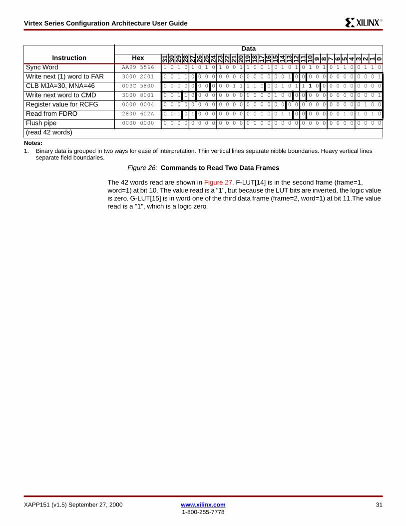
Virtex Series Configuration Architecture User GuideR13
The 42 words read are shown in Figure 27 F-LUT[14] is in the second frame (frame=1word=1) at bit 10 The value read is a 1 but because the LUT bits are inverted the logic valueis zero G-LUT[15] is in word one of the third data frame (frame=2 word=1) at bit 11The valueread is a 1 which is a logic zero
InstructionData
Hex 31 30 29 28 27 26 25 24 23 22 21 20 19 18 17 16 15 14 13 12 11 10 9 8 7 6 5 4 3 2 1 0
Sync Word AA99 5566 1 0 1 0 1 0 1 0 1 0 0 1 1 0 0 1 0 1 0 1 0 1 0 1 0 1 1 0 0 1 1 0
Write next (1) word to FAR 3000 2001 0 0 1 1 0 0 0 0 0 0 0 0 0 0 0 0 0 0 1 0 0 0 0 0 0 0 0 0 0 0 0 1
CLB MJA=30 MNA=46 003C 5800 0 0 0 0 0 0 0 0 0 0 1 1 1 1 0 0 0 1 0 1 1 1 0 0 0 0 0 0 0 0 0 0
Write next word to CMD 3000 8001 0 0 1 1 0 0 0 0 0 0 0 0 0 0 0 0 1 0 0 0 0 0 0 0 0 0 0 0 0 0 0 1
Register value for RCFG 0000 0004 0 0 0 0 0 0 0 0 0 0 0 0 0 0 0 0 0 0 0 0 0 0 0 0 0 0 0 0 0 1 0 0
Read from FDRO 2800 602A 0 0 1 0 1 0 0 0 0 0 0 0 0 0 0 0 0 1 1 0 0 0 0 0 0 0 1 0 1 0 1 0
Flush pipe 0000 0000 0 0 0 0 0 0 0 0 0 0 0 0 0 0 0 0 0 0 0 0 0 0 0 0 0 0 0 0 0 0 0 0
(read 42 words)
Notes1 Binary data is grouped in two ways for ease of interpretation Thin vertical lines separate nibble boundaries Heavy vertical lines
separate field boundaries
Figure 26 Commands to Read Two Data Frames
XAPP151 (v15) September 27 2000 wwwxilinxcom 311-800-255-7778
Virtex Series Configuration Architecture User GuideR13
To write to the F-LUT semaphore start with the second data frame (frame=1) that was justread Words 1 - 13 of that frame will become words 0 - 12 of the frame to be written Word 13of this new frame is a pad word and can have any value (typically 0 is chosen) In this newframe set bit 11 of word 0 (zero) to the desired value of the semaphore A pad frame mustfollow the data frame The commands from Figure 28 write these two frames into the device atthe proper location
Frame Word 31 30 29 28 27 26 25 24 23 22 21 20 19 18 17 16 15 14 13 12 11 10 9 8 7 6 5 4 3 2 1 0
0
0 1 1 1 1 1 1 1 1 1 1 1 1 1 1 1 1 1 1 1 1 1 1 1 1 1 1 1 1 1 1 1 1
1 1 1 1 1 1 1 1 1 1 1 1 1 1 1 1 1 1 1 1 1 1 1 1 1 1 1 1 1 1 1 1 1
2 1 1 1 1 1 1 1 1 1 1 1 1 1 1 1 1 1 1 1 1 1 1 1 1 1 1 1 1 1 1 1 1
3 1 1 1 1 1 1 1 1 1 1 1 1 1 1 1 1 1 1 1 1 1 1 1 1 1 1 1 1 1 1 1 1
4 1 1 1 1 1 1 1 1 1 1 1 1 1 1 1 1 1 1 1 1 1 1 1 1 1 1 1 1 1 1 1 1
5 1 1 1 1 1 1 1 1 1 1 1 1 1 1 1 1 1 1 1 1 1 1 1 1 1 1 1 1 1 1 1 1
6 1 1 1 1 1 1 1 1 1 1 1 1 1 1 1 1 1 1 1 1 1 1 1 1 1 1 1 1 1 1 1 1
7 1 1 1 1 1 1 1 1 1 1 1 1 1 1 1 1 1 1 1 1 1 1 1 1 1 1 1 1 1 1 1 1
8 1 1 1 1 1 1 1 1 1 1 1 1 1 1 1 1 1 1 1 1 1 1 1 1 1 1 1 1 1 1 1 1
9 1 1 1 1 1 1 1 1 1 1 1 1 1 1 1 1 1 1 1 1 1 1 1 1 1 1 1 1 1 1 1 1
10 1 1 1 1 1 1 1 1 1 1 1 1 1 1 1 1 1 1 1 1 1 1 1 1 1 1 1 1 1 1 1 1
11 1 1 1 1 1 1 1 1 1 1 1 1 1 1 1 1 1 1 1 1 1 1 1 1 1 1 1 1 1 1 1 1
12 1 1 1 1 1 1 1 1 1 1 1 1 1 1 1 1 1 1 1 1 1 1 1 1 1 1 1 1 1 1 1 1
13 1 1 1 1 1 1 1 1 1 1 1 1 1 1 1 1 1 1 1 1 1 1 1 1 1 1 1 1 1 1 1 1
1
0 0 0 0 0 0 0 0 0 0 0 0 0 0 0 0 0 0 0 0 0 0 0 0 0 0 0 0 0 0 0 0 0
1 1 0 0 0 0 0 0 0 0 0 0 0 1 0 0 0 0 1 1 0 1 1 0 0 0 0 0 0 0 0 0 0 F[14]
2 1 1 1 1 1 0 1 1 0 0 0 0 1 1 1 1 0 0 1 1 1 1 1 0 1 1 0 0 0 0 0 0
3 0 0 0 0 1 1 1 1 1 0 1 1 0 0 0 0 0 0 0 0 0 0 1 1 1 1 1 0 1 1 0 0
4 0 0 0 0 0 0 0 0 1 1 1 1 0 0 0 0 0 0 0 0 0 0 0 0 0 0 1 1 1 1 1 0
5 1 1 0 0 1 1 0 0 0 0 0 0 1 1 0 0 1 0 1 1 0 0 0 0 0 0 0 0 0 0 1 1
6 1 1 1 0 1 1 0 0 0 0 0 0 1 1 1 0 1 1 1 0 1 0 1 1 0 0 0 0 0 0 0 0
7 0 0 1 1 1 1 1 0 1 1 0 0 0 0 1 1 0 0 0 0 1 1 1 1 1 0 1 1 0 0 0 0
8 0 0 0 0 0 0 1 1 1 1 1 0 0 0 0 0 0 0 0 0 0 0 0 0 1 1 1 1 1 0 1 1
9 0 0 0 0 0 0 0 0 0 0 1 1 0 0 0 0 1 1 0 0 0 0 0 0 0 0 0 0 1 1 1 1
10 1 0 1 1 0 0 0 0 0 0 0 0 1 0 1 1 1 1 1 0 1 1 0 0 0 0 0 0 0 0 0 0
11 1 1 1 1 1 0 1 1 0 0 0 0 1 1 1 1 0 0 1 1 1 1 1 0 1 1 0 0 0 0 0 0
12 0 0 0 0 1 1 0 1 1 0 1 1 0 0 0 0 0 0 0 0 0 0 1 1 1 1 1 0 0 0 0 0
13 0 0 0 0 0 0 1 1 0 1 0 1 0 0 0 0 0 0 0 0 0 0 0 0 0 0 0 0 0 0 0 0
2
0 0 0 0 0 0 0 0 0 0 0 0 0 0 0 0 0 0 0 0 0 0 0 0 0 0 0 0 0 0 0 0 0
1 1 0 1 0 0 0 0 0 0 0 0 1 1 0 1 0 1 1 1 0 1 1 0 0 0 0 0 0 0 0 0 0 G[15]
2 1 1 1 1 1 1 1 1 0 0 0 0 1 1 1 1 0 0 1 1 1 1 1 1 1 1 0 0 0 0 0 0
3 0 0 0 0 1 1 1 1 1 1 1 1 0 0 0 0 0 0 0 0 0 0 1 0 1 1 1 1 1 1 0 0
4 0 0 0 0 0 0 0 0 1 1 1 1 0 0 0 0 0 0 0 0 0 0 0 0 0 0 1 1 1 1 1 1
5 1 1 0 0 0 0 0 0 0 0 0 0 1 1 0 0 1 1 1 1 0 0 1 0 0 0 0 0 0 0 1 1
6 1 1 1 1 1 1 0 0 0 0 0 0 1 1 1 1 1 1 1 1 1 1 1 1 0 0 0 0 0 0 0 0
7 0 0 1 1 1 1 1 1 1 1 0 0 0 0 1 1 0 0 0 0 1 1 1 1 1 1 1 1 0 0 0 0
8 0 0 0 0 0 0 1 1 1 1 1 1 0 0 0 0 0 0 0 0 0 0 0 0 1 1 1 1 1 1 1 1
9 0 0 0 0 0 0 0 0 0 0 1 1 0 0 0 0 1 1 0 0 0 0 0 0 0 0 0 0 1 1 1 1
10 1 1 1 1 0 0 0 0 0 0 0 0 1 1 1 1 1 1 1 1 1 1 0 0 0 0 0 0 0 0 0 0
11 1 1 1 1 1 1 1 1 0 0 0 0 1 1 1 1 0 0 1 1 1 1 1 1 1 1 0 0 0 0 0 0
12 0 0 0 0 1 1 0 1 1 1 1 1 0 0 0 0 0 0 0 0 0 0 1 1 1 1 1 0 1 0 0 0
13 0 0 0 0 0 1 1 0 0 1 1 1 0 0 0 0 0 0 0 0 0 0 0 0 0 0 0 0 0 0 0 0
Figure 27 Three Frames Containing the Semaphores
32 wwwxilinxcom XAPP151 (v15) September 27 20001-800-255-7778
Virtex Series Configuration Architecture User GuideR13
Example 2 Reading the Complete Configuration from an XCV50Steps
1 If flip-flop values are needed clock the on-chip signal CAPTURE to capture flip-flopvalues See the Xilinx Libraries Guide for use of the CAPTURE_VIRTEX cell
2 Write the starting frame address (CLB MJA=0 MNA=0) into the FAR
3 Write the RCFG command to the CMD register
4 Address the FDRO register with a READ operation and word count equal to the number of32-bit words in the CLB frames plus one pad frame
5 Read the data following the timing diagrams in the SelectMAP interface section
6 Write the address for RAM block 0 to the FAR
7 Address the FDRO register with a read operation and word count equal to the number of32-bit words in the RAM block plus one pad frame
8 Read the data
9 Write the address for RAM block 1 to the FAR
10 Address the FDRO register with a read operation and word count equal to the number of32-bit words in the RAM block plus one pad frame
11 Read the data
When using SelectMAP mode to read data words from the Virtex device de-assert CS de-assert WRITE assert CS then clock the data out When using JTAG load the JTAG IR
InstructionData
Hex 31 30 29 28 27 26 25 24 23 22 21 20 19 18 17 16 15 14 13 12 11 10 9 8 7 6 5 4 3 2 1 0
Sync Word AA995566
1 0 1 0 1 0 1 0 1 0 0 1 1 0 0 1 0 1 0 1 0 1 0 1 0 1 1 0 0 1 1 0
Write next (1) word to FAR 30002001
0 0 1 1 0 0 0 0 0 0 0 0 0 0 0 0 0 0 1 0 0 0 0 0 0 0 0 0 0 0 0 1
MJA=30 MNA=46 003C5C00
0 0 0 0 0 0 0 0 0 0 1 1 1 1 0 0 0 1 0 1 1 1 0 0 0 0 0 0 0 0 0 0
Write next word to CMD 30008001
0 0 1 1 0 0 0 0 0 0 0 0 0 0 0 0 1 0 0 0 0 0 0 0 0 0 0 0 0 0 0 1
Register value for WCFG 00000001
0 0 0 0 0 0 0 0 0 0 0 0 0 0 0 0 0 0 0 0 0 0 0 0 0 0 0 0 0 0 0 1
Write 28 words to FDRI 3000401C
0 0 1 1 0 0 0 0 0 0 0 0 0 0 0 0 0 1 0 0 0 0 0 0 0 0 0 1 1 1 0 0
Data Word 0 A01AEC00
1 0 1 0 0 0 0 0 0 0 0 1 1 0 1 0 1 1 1 0 1 1 0 0 0 0 0 0 0 0 0 0
Data Word 1 FF0F3FC0
1 1 1 1 1 1 1 1 0 0 0 0 1 1 1 1 0 0 1 1 1 1 1 1 1 1 0 0 0 0 0 0
Data Word 2 0FF002FC
0 0 0 0 1 1 1 1 1 1 1 1 0 0 0 0 0 0 0 0 0 0 1 0 1 1 1 1 1 1 0 0
hellip hellip hellip
Data Word 27 00000000
0 0 0 0 0 0 0 0 0 0 0 0 0 0 0 0 0 0 0 0 0 0 0 0 0 0 0 0 0 0 0 0
Notes1 Binary data is grouped in two ways for ease of interpretation Thin vertical lines separate nibble boundaries Heavy
vertical lines separate field boundaries
Figure 28 Commands to Write a Semaphore Value
XAPP151 (v15) September 27 2000 wwwxilinxcom 331-800-255-7778
Virtex Series Configuration Architecture User GuideR13
(instruction register) with the CFG_OUT instruction Then go to the SDR (Shift-DR) state andshift the data out (See Figure 29)
Example 3 Read the Slice 0 G-LUT from CLB R1 C1 from the CompleteConfiguration of an XCV50The commands for reading the bitstream from the Virtex device are given in Example 1 Readand Write Semaphores in an XCV100 at CLB R1 C1 Slice 0 on page 28 Using an XCV50device the independent attributes are show in Table 28
InstructionData
Hex 31 30 29 28 27 26 25 24 23 22 21 20 19 18 17 16 15 14 13 12 11 10 9 8 7 6 5 4 3 2 1 0
Sync Word AA99 5566 1 0 1 0 1 0 1 0 1 0 0 1 1 0 0 1 0 1 0 1 0 1 0 1 0 1 1 0 0 1 1 0
Write next word to FAR 3000 2001 0 0 1 1 0 0 0 0 0 0 0 0 0 0 0 0 0 0 1 0 0 0 0 0 0 0 0 0 0 0 0 1
CLB MJA=0 MNA=0 0000 0000 0 0 0 0 0 0 0 0 0 0 0 0 0 0 0 0 0 0 0 0 0 0 0 0 0 0 0 0 0 0 0 0
Write next word to CMDregister
3000 8001 0 0 1 1 0 0 0 0 0 0 0 0 0 0 0 0 1 0 0 0 0 0 0 0 0 0 0 0 0 0 0 1
Register value for RCFG 0000 0004 0 0 0 0 0 0 0 0 0 0 0 0 0 0 0 0 0 0 0 0 0 0 0 0 0 0 0 0 0 1 0 0
Read from FDRO register 2800 6000 0 0 1 0 1 0 0 0 0 0 0 0 0 0 0 0 0 1 1 0 0 0 0 0 0 0 0 0 0 0 0 0
15876 words 4800 3E04 0 1 0 0 1 0 0 0 0 0 0 0 0 0 0 0 0 0 1 1 1 1 1 0 0 0 0 0 0 1 0 0
Flush pipe 0000 0000 0 0 0 0 0 0 0 0 0 0 0 0 0 0 0 0 0 0 0 0 0 0 0 0 0 0 0 0 0 0 0 0
(Read 15876 words)Write to FAR register 3000 2001 0 0 1 1 0 0 0 0 0 0 0 0 0 0 0 0 0 0 1 0 0 0 0 0 0 0 0 0 0 0 0 1
RAM MJA=0 MNA=0 0200 0000 0 0 0 0 0 0 1 0 0 0 0 0 0 0 0 0 0 0 0 0 0 0 0 0 0 0 0 0 0 0 0 0
Read 780 words fromFDRO reg
2800 630C 0 0 1 0 1 0 0 0 0 0 0 0 0 0 0 0 0 1 1 0 0 0 1 1 0 0 0 0 1 1 0 0
Flush pipe 0000 0000 0 0 0 0 0 0 0 0 0 0 0 0 0 0 0 0 0 0 0 0 0 0 0 0 0 0 0 0 0 0 0 0
(Read 780 words)Write to FAR register 3000 2001 0 0 1 1 0 0 0 0 0 0 0 0 0 0 0 0 0 0 1 0 0 0 0 0 0 0 0 0 0 0 0 1
RAM MJA=1 MNA=0 0202 0000 0 0 0 0 0 0 1 0 0 0 0 0 0 0 1 0 0 0 0 0 0 0 0 0 0 0 0 0 0 0 0 0
Read 780 words fromFDRO reg
2800 630C 0 0 1 0 1 0 0 0 0 0 0 0 0 0 0 0 0 1 1 0 0 0 1 1 0 0 0 0 1 1 0 0
Flush pipe 0000 0000 0 0 0 0 0 0 0 0 0 0 0 0 0 0 0 0 0 0 0 0 0 0 0 0 0 0 0 0 0 0 0 0
(Read 780 words)
Figure 29 Example 2 - Read Complete Configuration for XCV50
Table 28 XCV50 Independent Attributes
Independent Attributes Values
Chip_Rows 16
Chip_Cols 24
FL 12
CLB_Row 1
CLB_Col 1
FG 1
Slice 0
RW 1
34 wwwxilinxcom XAPP151 (v15) September 27 20001-800-255-7778
Virtex Series Configuration Architecture User GuideR13
From the equations given earlier in Table 7 calculating the range of values for fm_st_wdindicates that the word 13740 of the configuration is the starting word of the 12-word (FL=12)frame containing bit 0 of the G-LUT in Slice 0 of CLB R1C1 (Table 29)
The configuration bits for the given frame are as follows G-LUT[0] is in fm_wd=0 at bit 11
All 16 LUT SelectRAM bits are in the following words at the same bit index 11
Table 29 Variables Equations and Values for Slice 0 G-LUT
Variables Equations Values
MJA 1 le 242 rArr 24 ndash 1times 2 + 2 24
MNA 0 times (hellip) + lut_bit + 32 0 321 332 343 35
4 365 376 387 39
8 409 41
10 4211 43
12 4413 4514 4615 47
fm_bit_idx 3 + 18 times 1 ndash1 + RW times 32 52
fm_st_wd 12 times (8+ (24 ndash1) times 48 + [3247]) +1 x 12= 12 times (1112 + [3247]) +12= 13356 + 12 times 3247]
1374013920
fm_wd floor(5232) 1
fm_wd_bit_idx 31 + 32 ndash 52 11
BitstreamWord
Frame 32-bit Word FrameWord31 30 29 28 27 26 25 24 23 22 21 20 19 18 17 16 15 14 13 12 11 10 9 8 7 6 5 4 3 2 1 0
13740 0 0 0 0 0 0 0 0 0 0 0 0 0 0 0 0 0 0 0 0 0 0 0 0 0 0 0 0 0 0 0 0 013741 0 0 1 0 1 0 0 0 0 0 0 0 0 1 0 1 0 1 0 0 1 1 1 0 0 0 0 0 0 0 0 0 113742 1 0 1 1 0 0 1 1 0 0 0 0 0 0 0 0 0 0 1 0 1 1 0 0 1 1 0 0 0 0 0 0 213743 0 0 0 0 1 0 1 1 0 0 1 1 0 0 0 0 0 0 0 0 0 0 1 0 1 1 0 0 1 1 0 0 313744 0 0 0 0 0 0 0 0 1 0 1 1 0 0 1 1 0 0 0 0 0 0 0 0 0 0 1 0 1 1 0 0 413745 1 1 0 0 0 0 0 0 0 0 0 0 1 0 1 1 0 0 1 1 0 0 0 0 0 0 0 0 0 0 1 0 513746 1 1 0 0 1 1 0 0 0 0 0 0 0 0 0 0 1 0 1 1 0 0 1 1 0 0 0 0 0 0 0 0 613747 0 0 1 0 1 1 0 0 1 1 0 0 0 0 0 0 0 0 0 0 1 0 1 1 0 0 1 1 0 0 0 0 713748 0 0 0 0 0 0 1 0 1 1 0 0 1 1 0 0 0 0 0 0 0 0 0 0 1 0 1 1 0 0 1 1 813749 0 0 0 0 0 0 0 0 0 0 1 0 1 1 0 0 1 1 0 0 0 0 0 0 0 0 0 0 1 0 1 1 913750 0 0 1 1 0 0 0 0 0 0 0 0 0 0 1 0 1 1 0 0 1 0 1 0 0 0 0 0 0 0 0 0 1013751 0 1 0 1 0 0 0 0 0 0 0 0 0 0 0 0 0 0 0 0 0 0 0 0 0 0 0 0 0 0 0 0 11
Figure 30 Configuration Bits for Slice 0 CLB R1C1 G-LUT [0]
XAPP151 (v15) September 27 2000 wwwxilinxcom 351-800-255-7778
Virtex Series Configuration Architecture User GuideR13
The 16 bits are LUT[150]=0111111111111111 The LUT SelectRAM bits are inverted from theirlogic values The ldquologicalrdquo contents are LUT[150]=1000000000000000 Thus this G-LUTimplements a 4-input AND function
Example 4 Read the Slice 1 F-LUT from CLB R19 C16 from an XCV100Commands for reading the bitstream from the Virtex device are given in Figure 32 Use thefollowing independent attributes to find the given F-LUT
From the equations in Table 7 on page 11 calculating fm_st_wd indicates the starting wordwith respect to a configuration that starts at MJA=0 MNA=0 Because the frames we are
BitstreamWord
Frame 32-bit Word
LUT Bit31 30 29 28 27 26 25 24 23 22 21 20 19 18 17 16 15 14 13 12 11 10 9 8 7 6 5 4 3 2 1 0
13741 0 0 1 0 1 0 0 0 0 0 0 0 0 1 0 1 0 1 0 0 1 1 1 0 0 0 0 0 0 0 0 0 0
13753 1 0 1 0 0 0 0 0 0 0 0 0 0 0 0 1 0 0 0 1 1 1 0 0 0 0 0 0 0 0 0 0 1
13765 1 0 1 0 1 0 0 0 0 0 0 0 1 0 0 0 0 0 0 1 1 1 1 0 0 0 0 0 0 0 0 0 2
13777 0 0 0 0 1 0 0 0 0 0 0 1 1 1 0 1 1 0 1 0 1 1 0 0 0 0 0 0 0 0 0 0 3
13789 0 1 0 0 0 0 0 0 0 0 0 0 0 1 0 1 1 1 1 1 1 1 1 0 0 0 0 0 0 0 0 0 4
13801 1 0 1 0 1 0 0 0 0 0 0 1 0 0 0 1 1 0 0 1 1 1 0 0 0 0 0 0 0 0 0 0 5
13813 0 0 0 1 0 0 0 0 0 0 0 0 0 0 0 0 1 0 0 1 1 1 0 0 0 0 0 0 0 0 0 0 6
13825 0 1 1 0 1 0 0 0 0 0 0 1 0 1 0 0 1 1 0 0 1 1 0 0 0 0 0 0 0 0 0 0 7
13837 1 0 1 1 1 0 0 0 0 0 0 1 0 1 0 1 1 0 0 0 1 1 0 0 0 0 0 0 0 0 0 0 8
13849 1 0 0 0 0 0 0 0 0 0 0 0 0 0 0 0 1 1 1 0 1 1 0 0 0 0 0 0 0 0 0 0 9
13861 1 0 0 0 0 0 0 0 0 0 0 1 0 0 0 0 1 1 1 1 1 1 1 0 0 0 0 0 0 0 0 0 10
13873 1 0 0 0 0 0 0 1 0 0 0 0 0 1 0 0 0 1 1 0 1 1 0 0 0 1 0 0 0 0 0 0 11
13885 1 0 0 0 0 0 0 0 0 0 0 0 0 1 0 1 0 0 1 0 1 1 0 0 0 0 0 0 0 0 0 0 12
13897 0 0 0 0 1 0 0 0 0 0 0 0 0 1 0 0 0 0 0 0 1 1 0 0 0 0 0 0 0 0 0 0 13
13909 1 0 0 0 0 0 0 0 0 0 0 0 1 1 0 1 0 1 1 0 1 1 0 0 0 0 0 0 0 0 0 0 14
13921 1 0 1 0 0 0 0 0 0 0 0 1 1 1 0 1 1 1 1 1 0 1 0 0 0 0 0 0 0 0 0 0 15
Figure 31 Location of all 16 LUT SelectRAM Bits
Table 30 Virtex Bitstream Command Attributes
Independent Attributes Values
Chip_Rows 20
Chip_Cols 30
FL 14
CLB_Row 19
CLB_Col 16
FG 0
Slice 1
RW 1
36 wwwxilinxcom XAPP151 (v15) September 27 20001-800-255-7778
Virtex Series Configuration Architecture User GuideR13
interested in start at MJA=1 MNA=0 which is fm_st_wd = 126 so the first 126 words are notneeded (0ndash125) Therefore to find the given Slice 1 F-LUT see Table 31
Sixteen frames need to be read one for each bit in the LUT SelectRAM The bits in LUTSelectRAMs in Slice 1 occur in the opposite order that they do for Slice 0 LUT SelectRAMs
Frames are read sequentially with ascending addresses If read in LUT bit order LUT[0]LUT[1] hellip LUT[15] These are stored in descending addresses which require 16 separateread operations each reading one data frame and one pad frame However if read inascending address order LUT[15] LUT[14] hellip LUT[0] all 16 data frames are read with asingle read operation This requires only one pad frame for all 16 frames Thus it takes lesstime to read ascending frames starting at MJA=1 MNA=0 and finishing with frame MJA=1MNA=15 The frames in the XCV100 contain 14 32-bit words and a single pad wordCommands for reading only the F-LUT data are given in Figure 32
Table 31 Variables Equations and Values for Slice 1 F-LUT
Variables Equations Values
MJA 16 gt 302 rArr 2times16 ndash 30 ndash1 1
MNA lut_bit + 32 ndash Slice times (2 times lut_bit +17)= [015] + 32 ndash (2 times [015] + 17)= 15 ndash [015]
0 151 142 133 12
4 115 106 97 8
8 79 6
10 511 4
12 313 214 115 0
fm_bit_idx 3 + 18 times 19 ndash 0+ 32 377
fm_st_wd 14 times (8 + (1ndash 1) times 48 + [150]) +1 times 14= 14 times (8 + [150]) +14= 126 + 14 times [150]
= 336126
fm_wd floor(37732) 11
fm_wd_bit_idx 31 + 32 times 11 ndash 377 6
XAPP151 (v15) September 27 2000 wwwxilinxcom 371-800-255-7778
Virtex Series Configuration Architecture User GuideR13
The 377th bit of each frame is the bit in the F-LUT This LUT SelectRAM bit is in the framersquosword index 11 bit index 6
The configuration bits for the given frame in Figure 33 are as follows LUT Bit 15 is in MJA=1MNA=0 fm_wd=11 at bit 6
LUT bit 0 is in MJA=1 MNA=15 fm_wd=11 at bit 6
InstructionData
Hex 31 30 29 28 27 26 25 24 23 22 21 20 19 18 17 16 15 14 13 12 11 10 9 8 7 6 5 4 3 2 1 0
Sync Word AA99 5566 1 0 1 0 1 0 1 0 1 0 0 1 1 0 0 1 0 1 0 1 0 1 0 1 0 1 1 0 0 1 1 0
Write next (1) word to FAR 3000 2001 0 0 1 1 0 0 0 0 0 0 0 0 0 0 0 0 0 0 1 0 0 0 0 0 0 0 0 0 0 0 0 1
CLB MJA = 1 MNA = 0 0002 0000 0 0 0 0 0 0 0 0 0 0 0 0 0 0 1 0 0 0 0 0 0 0 0 0 0 0 0 0 0 0 0 0
Write next word to CMD 3000 8001 0 0 1 1 0 0 0 0 0 0 0 0 0 0 0 0 1 0 0 0 0 0 0 0 0 0 0 0 0 0 0 1
Register value for RCFG 0000 0004 0 0 0 0 0 0 0 0 0 0 0 0 0 0 0 0 0 0 0 0 0 0 0 0 0 0 0 0 0 1 0 0
Read from FDRO 2800 60EE 0 0 1 0 1 0 0 0 0 0 0 0 0 0 0 0 0 1 1 0 0 0 0 0 1 1 1 0 1 1 1 0
Flush pipe 0000 0000 0 0 0 0 0 0 0 0 0 0 0 0 0 0 0 0 0 0 0 0 0 0 0 0 0 0 0 0 0 0 0 0
(Read 238 words)
Figure 32 Commands to read Slice 1 F-LUT
Frame WordFrame 32-bit Word
31 30 29 28 27 26 25 24 23 22 21 20 19 18 17 16 15 14 13 12 11 10 9 8 7 6 5 4 3 2 1 0
0 0 0 0 0 0 0 0 0 0 0 0 0 0 0 0 0 0 0 0 0 0 0 0 0 0 0 0 0 0 0 0 0
1 1 1 0 0 0 0 0 0 0 0 0 0 0 1 0 1 1 1 1 1 1 1 0 0 0 0 0 0 0 0 0 0
2 1 1 1 1 1 1 1 1 0 0 0 0 0 0 0 0 0 0 1 1 1 1 1 1 1 1 0 0 0 0 0 0
3 0 0 0 0 1 1 1 1 1 1 1 1 0 0 0 0 0 0 0 0 0 0 1 1 1 1 1 1 1 1 0 0
4 0 0 0 0 0 0 0 0 1 1 1 1 1 1 1 1 0 0 0 0 0 0 0 0 0 0 1 1 1 1 1 1
5 1 1 0 0 0 0 0 0 0 0 0 0 1 1 1 1 1 1 1 1 0 0 0 0 0 0 0 0 0 0 1 1
6 1 1 1 1 1 1 0 0 0 0 0 0 0 0 0 0 1 1 1 1 1 1 1 1 0 0 0 0 0 0 0 0
7 0 0 1 1 1 1 1 1 1 1 0 0 0 0 0 0 0 0 0 0 1 1 1 1 1 1 1 1 0 0 0 0
8 0 0 0 0 0 0 1 1 1 1 1 1 1 1 0 0 0 0 0 0 0 0 0 0 1 1 1 1 1 1 1 1
9 0 0 0 0 0 0 0 0 0 0 1 1 1 1 1 1 1 1 0 0 0 0 0 0 0 0 0 0 1 1 1 1
10 1 1 1 1 0 0 0 0 0 0 0 0 0 0 1 1 1 1 1 1 1 1 0 0 0 0 0 0 0 0 0 0
11 1 1 1 1 1 1 1 1 0 0 0 0 0 0 0 0 0 0 1 1 1 1 1 1 1 0 0 0 0 0 0 0
12 0 0 0 0 1 1 1 1 1 1 1 1 0 0 0 0 0 0 0 0 0 0 1 1 1 1 1 1 0 0 0 0
13 0 0 0 0 0 0 0 0 0 1 1 1 0 0 0 0 0 0 0 0 0 0 1 1 1 1 1 1 0 0 0 0
Figure 33 Frame Containing F-LUT[15]
Bit streamWord
Frame 32-bit WordFmWd31 30 29 28 27 26 25 24 23 22 21 20 19 18 17 16 15 14 13 12 11 10 9 8 7 6 5 4 3 2 1 0
336 0 0 0 0 0 0 0 0 0 0 0 0 0 0 0 0 0 0 0 0 0 0 0 0 0 0 0 0 0 0 0 0 0337 0 1 0 0 1 0 0 0 0 0 0 1 0 1 0 0 1 1 0 0 1 1 0 0 0 0 0 0 0 0 0 0 1338 1 0 1 1 0 0 1 1 0 0 0 0 0 0 0 0 0 0 1 0 1 1 0 0 1 1 0 0 0 0 0 0 2339 0 0 0 0 1 0 1 1 0 0 1 1 0 0 0 0 0 0 0 0 0 0 1 0 1 1 0 0 1 1 0 0 3340 0 0 0 0 0 0 0 0 1 0 1 1 0 0 1 1 0 0 0 0 0 0 0 0 0 0 1 0 1 1 0 0 4341 1 1 0 0 0 0 0 0 0 0 0 0 1 0 1 1 0 0 1 1 0 0 0 0 0 0 0 0 0 0 1 0 5342 1 1 0 0 1 1 0 0 0 0 0 0 0 0 0 0 1 0 1 1 0 0 1 1 0 0 0 0 0 0 0 0 6343 0 0 1 0 1 1 0 0 1 1 0 0 0 0 0 0 0 0 0 0 1 0 1 1 0 0 1 1 0 0 0 0 7
Figure 34 Frame Containing F-LUT [0]
38 wwwxilinxcom XAPP151 (v15) September 27 20001-800-255-7778
Virtex Series Configuration Architecture User GuideR13
For the sake of brevity here are the sixteen 11th words in the order they appear in thebitstream
The bits are LUT[150]=0111111111111111 The LUT SelectRAM bits are inverted from thelogic sense The logical contents are LUT[150]=1000000000000000 Thus this F-LUTimplements a 4-input AND gate
Example 5 Read All Bits in Slice 0 G-LUTs from CLB C2 and XCV50Given the following attributes the necessary values to find the G-LUT data can be computed
344 0 0 0 0 0 0 1 0 1 1 0 0 1 1 0 0 0 0 0 0 0 0 0 0 1 0 1 1 0 0 1 1 8345 0 0 0 0 0 0 0 0 0 0 1 0 1 1 0 0 1 1 0 0 0 0 0 0 0 0 0 0 1 0 1 1 9346 0 0 1 1 0 0 0 0 0 0 0 0 0 0 1 0 1 1 0 0 1 1 0 0 0 0 0 0 0 0 0 0 10347 1 1 1 1 1 0 1 1 0 0 0 0 0 0 0 0 0 0 1 0 1 1 1 0 1 1 0 1 0 0 0 0 11348 0 0 0 0 1 1 1 0 1 0 1 1 0 0 0 0 0 0 0 0 0 0 1 1 1 1 0 1 0 0 0 0 12349 0 0 0 0 0 1 0 0 0 0 1 0 0 0 0 0 0 0 0 0 0 0 0 0 0 0 0 0 0 0 0 0 13
Bit streamWord
Frame 32-bit WordFmWd31 30 29 28 27 26 25 24 23 22 21 20 19 18 17 16 15 14 13 12 11 10 9 8 7 6 5 4 3 2 1 0
Figure 34 Frame Containing F-LUT [0]
BitstreamWord
Frame 32-bit WordLUT Bit31 30 29 28 27 26 25 24 23 22 21 20 19 18 17 16 15 14 13 12 11 10 9 8 7 6 5 4 3 2 1 0
137 1 1 1 1 1 1 1 1 0 0 0 0 0 0 0 0 0 0 1 1 1 1 1 1 1 0 0 0 0 0 0 0 15151 1 0 1 1 1 0 1 1 0 0 0 0 0 0 0 0 0 0 1 0 1 1 1 0 1 1 0 0 0 0 0 0 14165 1 0 1 1 0 0 1 1 0 0 0 0 0 0 0 0 0 0 1 0 1 1 1 0 1 1 0 0 0 0 0 0 13179 1 0 1 1 1 0 1 1 0 0 0 0 0 0 0 0 0 0 1 0 1 1 1 0 1 1 0 0 0 0 0 0 12193 1 1 1 1 1 0 1 1 0 0 0 0 0 0 0 0 0 0 1 1 1 1 1 0 1 1 0 0 0 0 0 0 11207 1 1 1 1 1 1 1 1 0 0 0 0 0 0 0 0 0 0 1 1 1 1 1 1 1 1 1 0 1 0 0 0 10221 1 1 1 1 1 0 1 1 0 0 0 0 0 0 0 0 0 0 1 1 1 1 1 0 1 1 0 0 0 0 0 0 9235 1 0 1 1 1 0 1 1 0 0 0 0 0 0 0 0 0 0 1 0 1 1 1 0 1 1 0 0 0 0 0 0 8249 1 0 1 1 0 0 1 1 0 0 0 0 0 0 0 0 0 0 1 0 1 1 0 0 1 1 0 0 0 0 0 0 7263 1 0 1 1 0 1 1 1 1 0 0 0 0 0 0 0 0 0 1 0 1 1 0 1 1 1 0 0 0 0 0 0 6277 1 1 1 1 0 0 1 1 0 0 0 0 0 0 0 0 0 0 1 1 1 1 0 0 1 1 0 0 0 0 0 0 5291 1 1 1 1 1 1 1 1 0 0 0 0 0 0 0 0 0 0 1 1 1 1 1 1 1 1 0 0 0 0 0 0 4305 1 1 1 1 1 0 1 1 0 0 0 0 0 0 0 0 0 0 1 1 1 1 1 0 1 1 0 0 0 0 0 0 3319 1 0 1 1 0 1 1 1 0 0 0 0 0 0 0 0 0 0 1 0 1 1 0 1 1 1 0 0 0 0 0 0 2333 1 0 1 1 0 0 1 1 0 0 0 0 0 0 0 0 0 0 1 0 1 1 0 0 1 1 0 0 0 0 0 0 1347 1 1 1 1 1 0 1 1 0 0 0 0 0 0 0 0 0 0 1 0 1 1 1 0 1 1 0 1 0 0 0 0 0
Figure 35 Sixteen Words Containing the F-LUT bit
Table 32 All Bits Slice 0 GndashLUTs from CLB C2 and XCV50
Independent Attributes Values
Chip_Rows 16
Chip_Cols 24
FL 12
CLB_Row 116
CLB_Col 2
XAPP151 (v15) September 27 2000 wwwxilinxcom 391-800-255-7778
Virtex Series Configuration Architecture User GuideR13
From the equations in Table 7 the dependent variables can be calculated
Note that fm_bit_idx fm_wd and fm_wd_bit_idx have 16 values one for each row on theXCV50 Figure 37 shows where the data lies in the first frame which contains G[0] for the entirecolumn The process is the same for the other 15 frames The commands for reading the LUTSelectRAM data are given in Figure 36
From the calculation for fm_st_wd Frame 0 would start at word 12588 reading the wholeconfiguration The instructions in Figure 36 start at that word so word 0 (ignoring the 12 wordsin the pad frame) is the same as word 12588 of the entire CLB configuration The 12 words inthe frame are shown in Figure 37
FG 1
Slice 0
lut_bit 015
RW 1
Table 32 All Bits Slice 0 GndashLUTs from CLB C2 and XCV50 (Continued)
Independent Attributes Values
Table 33 Dependent Variables Equations and Values
Variables Equations Values
MJA 2 le 242 rArr 24 ndash 2times 2 + 2 22
MNAlut_bit + 32 ndash Slice times (2 times lut_bit + 17)= lut_bit + 32 ndash 0 times (2 times lut_bit + 17)= [015] + 32
032 436 840 1244
133 537 941 1345
234 638 1042 1456
335 739 1143 1547
fm_bit_idx3 + 18 times CLB_Row ndash 1+ 32 = 34 + 18 times[116]
152 5124 9196 13268
270 6142 10214 14286
388 7160 11232 15304
4106 8178 12250 16322
fm_st_wd12 times (8 + (22 ndash1) times 48 + MNA) + 1 times 12= 12 times (1016 + MNA) + 12= 12204 + 12 times MNA
0 12588 4 12636 8 12684 12 12732
1 12600 5 12648 9 12696 13 12744
2 12612 6 12660 10 12708 14 12756
3 12624 7 12672 11 12720 15 12768
fm_wd floor (fm_bit_idx32)
11 53 96 138
22 64 106 148
32 75 117 159
43 85 127 1610
fm_wd_bit_idx 31 + 32 times fm_wd ndash fm_bit_idx
111 53 927 1319
225 617 109 141
37 7 31 1123 1515
421 813 125 1629
40 wwwxilinxcom XAPP151 (v15) September 27 20001-800-255-7778
Virtex Series Configuration Architecture User GuideR13
The LUT SelectRAM bits have been shaded for ease of identification It can be seen from thecalculation of fm_bit_idx that the LUT SelectRAM bits are in the order 116 For example fromthe above calculations for fm_wd and fm_wd_bit_idx G-LUT[0] in R1C2 is in fm_wd 1fm_wd_bit_idx 11 This bit is the shaded bit in word 1 at bit index 11 Similarly the G-LUT[0] forthe other 15 CLB rows are also shaded in this table
Example 6 Read Block SelectRAM index 387 of RAM R2 C0 from anXCV100ECommands for reading the bitstream from the Virtex device are given in Figure 38 Use thefollowing independent attributes to find the given F-LUT
InstructionData
Hex 31 30 29 28 27 26 25 24 23 22 21 20 19 18 17 16 15 14 13 12 11 10 9 8 7 6 5 4 3 2 1 0
Sync Word AA99 5566 1 0 1 0 1 0 1 0 1 0 0 1 1 0 0 1 0 1 0 1 0 1 0 1 0 1 1 0 0 1 1 0
Write next (1) word to FAR 3000 2001 0 0 1 1 0 0 0 0 0 0 0 0 0 0 0 0 0 0 1 0 0 0 0 0 0 0 0 0 0 0 0 1
CLB MJA=22 MNA=32 002C 4000 0 0 0 0 0 0 0 0 0 0 1 0 1 1 0 0 0 1 0 0 0 0 0 0 0 0 0 0 0 0 0 0
Write next word to CMD 3000 8001 0 0 1 1 0 0 0 0 0 0 0 0 0 0 0 0 1 0 0 0 0 0 0 0 0 0 0 0 0 0 0 1
Register value for RCFG 0000 0004 0 0 0 0 0 0 0 0 0 0 0 0 0 0 0 0 0 0 0 0 0 0 0 0 0 0 0 0 0 1 0 0
Read from FDRO 2800 60CC 0 0 1 0 1 0 0 0 0 0 0 0 0 0 0 0 0 1 1 0 0 0 0 0 1 1 0 0 1 1 0 0
Flush pipe 0000 0000 0 0 0 0 0 0 0 0 0 0 0 0 0 0 0 0 0 0 0 0 0 0 0 0 0 0 0 0 0 0 0 0
(Read 204 words)
Figure 36 Commands to read RC2S0 G-LUT
WordFrame 32-bit Word
CLB Row31 30 29 28 27 26 25 24 23 22 21 20 19 18 17 16 15 14 13 12 11 10 9 8 7 6 5 4 3 2 1 0
0 0 0 0 0 0 0 0 0 0 0 0 0 0 0 0 0 0 0 0 0 0 0 0 0 0 0 0 0 0 0 0 0
1 0 0 0 0 1 0 0 0 0 0 0 0 0 1 0 1 0 1 0 0 1 1 0 0 0 0 0 0 0 0 0 0 12 1 0 1 1 0 0 1 1 0 0 0 0 0 0 0 0 0 0 1 0 1 1 0 0 1 1 0 0 0 0 0 0 2 33 0 0 0 0 1 0 1 1 0 0 1 1 0 0 0 0 0 0 0 0 0 0 1 0 1 1 0 0 1 1 0 0 4 54 0 0 0 0 0 0 0 0 1 0 1 1 0 0 1 1 0 0 0 0 0 0 0 0 0 0 1 0 1 1 0 0 65 1 1 0 0 0 0 0 0 0 0 0 0 1 0 1 1 0 0 1 1 0 0 0 0 0 0 0 0 0 0 1 0 7 86 1 1 0 0 1 1 0 0 0 0 0 0 0 0 0 0 1 0 1 1 0 0 1 1 0 0 0 0 0 0 0 0 9 107 0 0 1 0 1 1 0 0 1 1 0 0 0 0 0 0 0 0 0 0 1 0 1 1 0 0 1 1 0 0 0 0 11 128 0 0 0 0 0 0 1 0 1 1 0 0 1 1 0 0 0 0 0 0 0 0 0 0 1 0 1 1 0 0 1 1 13 149 0 0 0 0 0 0 0 0 0 0 1 0 1 1 0 0 1 1 0 0 0 0 0 0 0 0 0 0 1 0 1 1 15
10 0 0 1 1 0 0 0 0 0 0 0 0 0 0 1 0 1 1 0 0 1 0 1 0 0 0 0 0 0 0 0 0 1611 0 1 0 1 0 0 0 0 0 0 0 0 0 0 0 0 0 0 0 0 0 0 0 0 0 0 0 0 0 0 0 0
Figure 37 Frame for RC2S0 G-LUTs Bit G[0]
Table 34 Virtex Bitstream Command Attributes
Independent Attributes Values
Chip_Rams 4
FL 14
RAM_Row 2
RAM_Col 0
ram_bit 387
RW 1
XAPP151 (v15) September 27 2000 wwwxilinxcom 411-800-255-7778
Virtex Series Configuration Architecture User GuideR13
Since we are attempting to read only one bit location only one frame is necessary to be readWe use the equations of Table 15 Table 16 and Table 17 to determine the dependentvariables
Commands for reading this memory index are given in Figure 38
RAM bit 387 is at fm_wd=6 bit 4
Table 35 Variables Equations and Values for Slice 1 F-LUT
Variables Equations Values
MJA_virtex 0 lt42 rArr 2times(42 -1 -0) 2
MJA_adj 0 lt42 rArr 2 2
MJA MJA_virtex + MJA_adj 4
MNA floor(((38764)64)32)+ 2 x floor(((38764)32)16)+ 4 x floor(((38764)16)8) + 8 x floor(((38764)8)4)+ 16 x floor(((38764)4)2) + 32 x floor(((38764)2)1)
24
fm_bit_idx 3 + 18 times 19 ndash 0 + 32 219
fm_st_wd 14 x 24 + 1 x 14 350
fm_wd floor(21932) 6
fm_wd_bit_idx 31 + 32 times 6 ndash 219 4
InstructionData
Hex 31 30 29 28 27 26 25 24 23 22 21 20 19 18 17 16 15 14 13 12 11 10 9 8 7 6 5 4 3 2 1 0
Sync Word AA99 5566 1 0 1 0 1 0 1 0 1 0 0 1 1 0 0 1 0 1 0 1 0 1 0 1 0 1 1 0 0 1 1 0
Write next (1) word to FAR 3000 2001 0 0 1 1 0 0 0 0 0 0 0 0 0 0 0 0 0 0 1 0 0 0 0 0 0 0 0 0 0 0 0 1
CLB MJA = 4 MNA = 24 0208 3000 0 0 0 0 0 0 1 0 0 0 0 0 1 0 0 0 0 0 1 1 0 0 0 0 0 0 0 0 0 0 0 0
Write next word to CMD 3000 8001 0 0 1 1 0 0 0 0 0 0 0 0 0 0 0 0 1 0 0 0 0 0 0 0 0 0 0 0 0 0 0 1
Register value for RCFG 0000 0004 0 0 0 0 0 0 0 0 0 0 0 0 0 0 0 0 0 0 0 0 0 0 0 0 0 0 0 0 0 1 0 0
Read from FDRO 2800 601C 0 0 1 0 1 0 0 0 0 0 0 0 0 0 0 0 0 1 1 0 0 0 0 0 0 0 0 1 1 1 0 0
Flush pipe 0000 0000 0 0 0 0 0 0 0 0 0 0 0 0 0 0 0 0 0 0 0 0 0 0 0 0 0 0 0 0 0 0 0 0
(Read 28 words)
Figure 38 Commands to read Block SelectRAM index 387
42 wwwxilinxcom XAPP151 (v15) September 27 20001-800-255-7778
Virtex Series Configuration Architecture User GuideR13
Glossary Block SelectRAM Resource
One of several large fully-synchronous dual-port memories in the Virtex FPGAs Each ofthese memories contain 4096 bits The organization of each memory is configurable Theblock SelectRAM resource complements the smaller distributed LUT SelectRAMs
Boundary Scan Interface
One of the configuration interfaces on the Virtex device This is a bit-serial interface TheBoundary Scan interface is also known as the JTAG port Also see the SelectMAP interface
Capture Data
The flip-flop and pad data saved from the logic cells and IO blocks into the bitstream Use theCAPTURE_VIRTEX primitive in your HDL code to specify the trigger and clock for the captureoperation
Configurable Logic Block (CLB)
The functional elements for constructing logic circuits The Virtex CLB is made up of Sliceswhich contain Logic Cells
Configuration Bitstream
Configuration commands optionally with configuration data
Configuration Commands
Instructions for the Virtex device There are two classes of Configuration Command mdash Majorand Minor The Major Commands read and write data to configuration registers in the Virtexdevice The Minor commands instruct the Virtex configuration logic to perform specificfunctions See Command Register (CMD) on page 18
Configuration Data
Bits that directly define the state of programmable logic These are written to a Virtex device ina configuration bitstream and read as Readback Data from a Virtex device
Frame WordFrame 32-bit Word
31 30 29 28 27 26 25 24 23 22 21 20 19 18 17 16 15 14 13 12 11 10 9 8 7 6 5 4 3 2 1 0
0 0 0 0 0 0 0 0 0 0 0 0 0 0 0 0 0 0 0 0 0 0 0 0 0 0 0 0 0 0 0 0 0
1 1 1 0 0 0 0 0 0 0 0 0 0 0 1 0 1 1 1 1 1 1 1 0 0 0 0 0 0 0 0 0 0
2 1 1 1 1 1 1 1 1 0 0 0 0 0 0 0 0 0 0 1 1 1 1 1 1 1 1 0 0 0 0 0 0
3 0 0 0 0 1 1 1 1 1 1 1 1 0 0 0 0 0 0 0 0 0 0 1 1 1 1 1 1 1 1 0 0
4 0 0 0 0 0 0 0 0 1 1 1 1 1 1 1 1 0 0 0 0 0 0 0 0 0 0 1 1 1 1 1 1
5 1 1 0 0 0 0 0 0 0 0 0 0 1 1 1 1 1 1 1 1 0 0 0 0 0 0 0 0 0 0 1 1
6 1 1 1 1 1 1 0 0 0 0 0 0 0 0 0 0 1 1 1 1 1 1 1 1 0 0 0 0 0 0 0 0
7 0 0 1 1 1 1 1 1 1 1 0 0 0 0 0 0 0 0 0 0 1 1 1 1 1 1 1 1 0 0 0 0
8 0 0 0 0 0 0 1 1 1 1 1 1 1 1 0 0 0 0 0 0 0 0 0 0 1 1 1 1 1 1 1 1
9 0 0 0 0 0 0 0 0 0 0 1 1 1 1 1 1 1 1 0 0 0 0 0 0 0 0 0 0 1 1 1 1
10 1 1 1 1 0 0 0 0 0 0 0 0 0 0 1 1 1 1 1 1 1 1 0 0 0 0 0 0 0 0 0 0
11 1 1 1 1 1 1 1 1 0 0 0 0 0 0 0 0 0 0 1 1 1 1 1 1 1 0 0 0 0 0 0 0
12 0 0 0 0 1 1 1 1 1 1 1 1 0 0 0 0 0 0 0 0 0 0 1 1 1 1 1 1 0 0 0 0
13 0 0 0 0 0 0 0 0 0 1 1 1 0 0 0 0 0 0 0 0 0 0 1 1 1 1 1 1 0 0 0 0
Figure 39 Frame MNA=24
XAPP151 (v15) September 27 2000 wwwxilinxcom 431-800-255-7778
Virtex Series Configuration Architecture User GuideR13
Configuration Frame
The configuration bits in a Virtex device are organized in columns A column of CLBs with theIO blocks above and below the CLBs contain 48 frames of configuration bits The smallestnumber of bits that can be read or written through the configuration interfaces is one frame
Configuration Interface
A logical interface on the Virtex device through which configuration commands and data can beread and written A interface consists of one or more physical Device Pins
Configuration Readback
The operation of reading Configuration Data (also known as Readback Data) from a Virtexdevice
Device Pin
One of the electrical connections on the package containing the Virtex device
Frame
See Configuration Frame
Logic Cell (LC)
The basic building block of the Virtex CLB An LC includes a 4-input function generator carrylogic and a storage element
LUT SelectRAMs
Shallow RAM structures implemented in CLB Lookup Tables (LUTs) See also blockSelectRAM section
Pad
Pad bits are extra bits used to make the total number of bits in a frame an integral multiple of32 the number of bits in a configuration word A Pad Word is an extra word used at the end ofa Configuration Frame for pipelining A Pad Frame is an extra Configuration Frame used at thebeginning of a Configuration Readback and at the end of a Configuration Write for pipelining
Readback Data
Configuration data read from a Virtex device The data is organized as Configuration Frames
SelectMAP Interface
One of the configuration interfaces on the Virtex device This is a byte-serial interface The pinsin the SelectMAP interface may be used as user IO after configuration has been completed orremain configured as a configuration interface
Slice
A subdivision of the Virtex CLB There are two vertical slices in a Virtex CLB Each slicecontains two Logic Cells
Sync Word
A 32-bit word with a value that is used to synchronize the configuration logic
44 wwwxilinxcom XAPP151 (v15) September 27 20001-800-255-7778
Virtex Series Configuration Architecture User GuideR13
RevisionHistory
The following table shows the revision history for this document
Date Version Revision
061799 10 Initial Release
072799 11 Updated the following tables Table 5 equation for MNA Table 7equations for MJA amp fm_bit_idx
092099 12 Changes in page 5 Most formulae in Table 7 have been revisedDocumented pad capture value P Corrected bit locations inExamples
022200 13 Updated to include Virtex-E block SelectRAM Correctedfm_bit_idx (Right IOB) equations in Table 12 and fm_st_wddefinition Corrected CRC algorithm Various corrections inExamples Reformatted and edited document and figures
080300 14 Updated to include Virtex-EM devices in Table 3 and Table 24
092700 15 Added Partial Reconfiguration of CLB section and Figure 26
XAPP151 (v15) September 27 2000 wwwxilinxcom 451-800-255-7778
- Summary
- Introduction
-
- CLBs IOBs and Configurations
-
- Configuring Virtex Devices
- Reading Configuration Bits From a Virtex Device
-
- Configuration Columns
- Configuration Addressing
-
- Block Type Major Address Minor Address
-
- Virtex Major Addresses
- Virtex-EM Major Addresses
- Virtex-E Major Addresses
-
- Frames
-
- Frame Sizes
- Frame Organization
- Location of LUT SelectRAM Bits
-
- Configuration Data Operations
-
- Reading Configuration Data
- Writing Configuration Data
- Altering Configuration Data
-
- Definitions
- CLB LUT SelectRAM Dependent Variables
-
- Virtex-E CLB LUT SelectRAM Dependent Variables
- LUT SelectRAM Examples
-
- CLB Flip-Flop Dependent Variables
-
- Virtex-E CLB Flip-Flop Dependent Variables
-
- IOB Dependent Variables
-
- Virtex-E IOB Dependent Variables
-
- Block SelectRAM Dependent Variables
-
- Virtex-E Block SelectRAM Dependent Variables
-
- Configuration Logic Basics
-
- Configuration Data
- Configuration Flow
-
- For Initial Configuration
- Reading Configuration
- Writing Configuration
-
- Configuration Registers
-
- Command Register (CMD)
- Configuration Option Register (COR)
- Control Register (CTL)
- Cyclic Redundancy Check (CRC)
-
- CRC Algorithm
-
- Frame Address Register (FAR)
- Frame Data Input Register (FDRI)
- Frame Data Output Register (FDRO)
- Frame Length Register (FLR)
- Legacy Output Register (LOUT)
- Mask Register (MASK)
- Status Register (STAT)
-
- Configuration Interface
- Partial Reconfiguration of CLBs
- Examples
-
- Example 1 Read and Write Semaphores in an XCV100 at CLB R1 C1 Slice 0
- Example 2 Reading the Complete Configuration from an XCV50
- Example 3 Read the Slice 0 G-LUT from CLB R1 C1 from the Complete Configuration of an XCV50
- Example 4 Read the Slice 1 F-LUT from CLB R19 C16 from an XCV100
- Example 5 Read All Bits in Slice 0 G-LUTs from CLB C2 and XCV50
- Example 6 Read Block SelectRAM index 387 of RAM R2 C0 from an XCV100E
-
- Glossary
-
- Block SelectRAM Resource
- Boundary Scan Interface
- Capture Data
- Configurable Logic Block (CLB)
- Configuration Bitstream
- Configuration Commands
- Configuration Data
- Configuration Frame
- Configuration Interface
- Configuration Readback
- Device Pin
- Frame
- Logic Cell (LC)
- LUT SelectRAMs
- Pad
- Readback Data
- SelectMAP Interface
- Slice
- Sync Word
-
- Revision History
-
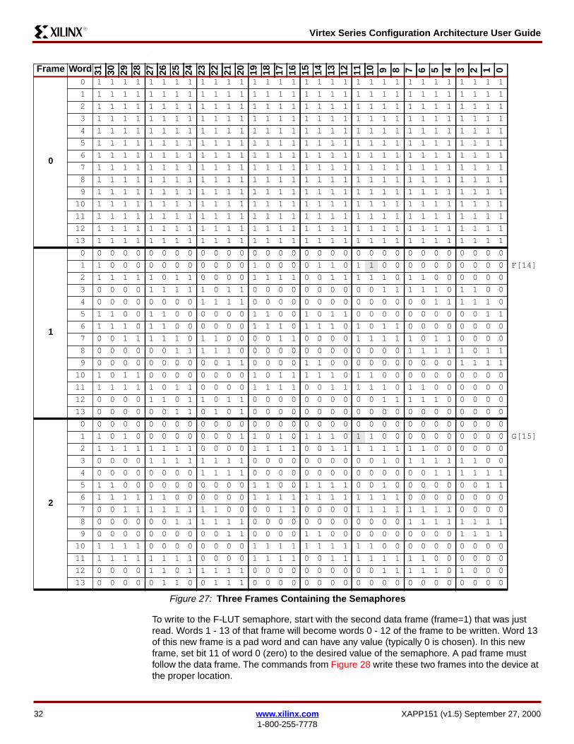
Virtex Series Configuration Architecture User GuideR13
Example 2 Reading the Complete Configuration from an XCV50Steps
1 If flip-flop values are needed clock the on-chip signal CAPTURE to capture flip-flopvalues See the Xilinx Libraries Guide for use of the CAPTURE_VIRTEX cell
2 Write the starting frame address (CLB MJA=0 MNA=0) into the FAR
3 Write the RCFG command to the CMD register
4 Address the FDRO register with a READ operation and word count equal to the number of32-bit words in the CLB frames plus one pad frame
5 Read the data following the timing diagrams in the SelectMAP interface section
6 Write the address for RAM block 0 to the FAR
7 Address the FDRO register with a read operation and word count equal to the number of32-bit words in the RAM block plus one pad frame
8 Read the data
9 Write the address for RAM block 1 to the FAR
10 Address the FDRO register with a read operation and word count equal to the number of32-bit words in the RAM block plus one pad frame
11 Read the data
When using SelectMAP mode to read data words from the Virtex device de-assert CS de-assert WRITE assert CS then clock the data out When using JTAG load the JTAG IR
InstructionData
Hex 31 30 29 28 27 26 25 24 23 22 21 20 19 18 17 16 15 14 13 12 11 10 9 8 7 6 5 4 3 2 1 0
Sync Word AA995566
1 0 1 0 1 0 1 0 1 0 0 1 1 0 0 1 0 1 0 1 0 1 0 1 0 1 1 0 0 1 1 0
Write next (1) word to FAR 30002001
0 0 1 1 0 0 0 0 0 0 0 0 0 0 0 0 0 0 1 0 0 0 0 0 0 0 0 0 0 0 0 1
MJA=30 MNA=46 003C5C00
0 0 0 0 0 0 0 0 0 0 1 1 1 1 0 0 0 1 0 1 1 1 0 0 0 0 0 0 0 0 0 0
Write next word to CMD 30008001
0 0 1 1 0 0 0 0 0 0 0 0 0 0 0 0 1 0 0 0 0 0 0 0 0 0 0 0 0 0 0 1
Register value for WCFG 00000001
0 0 0 0 0 0 0 0 0 0 0 0 0 0 0 0 0 0 0 0 0 0 0 0 0 0 0 0 0 0 0 1
Write 28 words to FDRI 3000401C
0 0 1 1 0 0 0 0 0 0 0 0 0 0 0 0 0 1 0 0 0 0 0 0 0 0 0 1 1 1 0 0
Data Word 0 A01AEC00
1 0 1 0 0 0 0 0 0 0 0 1 1 0 1 0 1 1 1 0 1 1 0 0 0 0 0 0 0 0 0 0
Data Word 1 FF0F3FC0
1 1 1 1 1 1 1 1 0 0 0 0 1 1 1 1 0 0 1 1 1 1 1 1 1 1 0 0 0 0 0 0
Data Word 2 0FF002FC
0 0 0 0 1 1 1 1 1 1 1 1 0 0 0 0 0 0 0 0 0 0 1 0 1 1 1 1 1 1 0 0
hellip hellip hellip
Data Word 27 00000000
0 0 0 0 0 0 0 0 0 0 0 0 0 0 0 0 0 0 0 0 0 0 0 0 0 0 0 0 0 0 0 0
Notes1 Binary data is grouped in two ways for ease of interpretation Thin vertical lines separate nibble boundaries Heavy
vertical lines separate field boundaries
Figure 28 Commands to Write a Semaphore Value
XAPP151 (v15) September 27 2000 wwwxilinxcom 331-800-255-7778
Virtex Series Configuration Architecture User GuideR13
(instruction register) with the CFG_OUT instruction Then go to the SDR (Shift-DR) state andshift the data out (See Figure 29)
Example 3 Read the Slice 0 G-LUT from CLB R1 C1 from the CompleteConfiguration of an XCV50The commands for reading the bitstream from the Virtex device are given in Example 1 Readand Write Semaphores in an XCV100 at CLB R1 C1 Slice 0 on page 28 Using an XCV50device the independent attributes are show in Table 28
InstructionData
Hex 31 30 29 28 27 26 25 24 23 22 21 20 19 18 17 16 15 14 13 12 11 10 9 8 7 6 5 4 3 2 1 0
Sync Word AA99 5566 1 0 1 0 1 0 1 0 1 0 0 1 1 0 0 1 0 1 0 1 0 1 0 1 0 1 1 0 0 1 1 0
Write next word to FAR 3000 2001 0 0 1 1 0 0 0 0 0 0 0 0 0 0 0 0 0 0 1 0 0 0 0 0 0 0 0 0 0 0 0 1
CLB MJA=0 MNA=0 0000 0000 0 0 0 0 0 0 0 0 0 0 0 0 0 0 0 0 0 0 0 0 0 0 0 0 0 0 0 0 0 0 0 0
Write next word to CMDregister
3000 8001 0 0 1 1 0 0 0 0 0 0 0 0 0 0 0 0 1 0 0 0 0 0 0 0 0 0 0 0 0 0 0 1
Register value for RCFG 0000 0004 0 0 0 0 0 0 0 0 0 0 0 0 0 0 0 0 0 0 0 0 0 0 0 0 0 0 0 0 0 1 0 0
Read from FDRO register 2800 6000 0 0 1 0 1 0 0 0 0 0 0 0 0 0 0 0 0 1 1 0 0 0 0 0 0 0 0 0 0 0 0 0
15876 words 4800 3E04 0 1 0 0 1 0 0 0 0 0 0 0 0 0 0 0 0 0 1 1 1 1 1 0 0 0 0 0 0 1 0 0
Flush pipe 0000 0000 0 0 0 0 0 0 0 0 0 0 0 0 0 0 0 0 0 0 0 0 0 0 0 0 0 0 0 0 0 0 0 0
(Read 15876 words)Write to FAR register 3000 2001 0 0 1 1 0 0 0 0 0 0 0 0 0 0 0 0 0 0 1 0 0 0 0 0 0 0 0 0 0 0 0 1
RAM MJA=0 MNA=0 0200 0000 0 0 0 0 0 0 1 0 0 0 0 0 0 0 0 0 0 0 0 0 0 0 0 0 0 0 0 0 0 0 0 0
Read 780 words fromFDRO reg
2800 630C 0 0 1 0 1 0 0 0 0 0 0 0 0 0 0 0 0 1 1 0 0 0 1 1 0 0 0 0 1 1 0 0
Flush pipe 0000 0000 0 0 0 0 0 0 0 0 0 0 0 0 0 0 0 0 0 0 0 0 0 0 0 0 0 0 0 0 0 0 0 0
(Read 780 words)Write to FAR register 3000 2001 0 0 1 1 0 0 0 0 0 0 0 0 0 0 0 0 0 0 1 0 0 0 0 0 0 0 0 0 0 0 0 1
RAM MJA=1 MNA=0 0202 0000 0 0 0 0 0 0 1 0 0 0 0 0 0 0 1 0 0 0 0 0 0 0 0 0 0 0 0 0 0 0 0 0
Read 780 words fromFDRO reg
2800 630C 0 0 1 0 1 0 0 0 0 0 0 0 0 0 0 0 0 1 1 0 0 0 1 1 0 0 0 0 1 1 0 0
Flush pipe 0000 0000 0 0 0 0 0 0 0 0 0 0 0 0 0 0 0 0 0 0 0 0 0 0 0 0 0 0 0 0 0 0 0 0
(Read 780 words)
Figure 29 Example 2 - Read Complete Configuration for XCV50
Table 28 XCV50 Independent Attributes
Independent Attributes Values
Chip_Rows 16
Chip_Cols 24
FL 12
CLB_Row 1
CLB_Col 1
FG 1
Slice 0
RW 1
34 wwwxilinxcom XAPP151 (v15) September 27 20001-800-255-7778
Virtex Series Configuration Architecture User GuideR13
From the equations given earlier in Table 7 calculating the range of values for fm_st_wdindicates that the word 13740 of the configuration is the starting word of the 12-word (FL=12)frame containing bit 0 of the G-LUT in Slice 0 of CLB R1C1 (Table 29)
The configuration bits for the given frame are as follows G-LUT[0] is in fm_wd=0 at bit 11
All 16 LUT SelectRAM bits are in the following words at the same bit index 11
Table 29 Variables Equations and Values for Slice 0 G-LUT
Variables Equations Values
MJA 1 le 242 rArr 24 ndash 1times 2 + 2 24
MNA 0 times (hellip) + lut_bit + 32 0 321 332 343 35
4 365 376 387 39
8 409 41
10 4211 43
12 4413 4514 4615 47
fm_bit_idx 3 + 18 times 1 ndash1 + RW times 32 52
fm_st_wd 12 times (8+ (24 ndash1) times 48 + [3247]) +1 x 12= 12 times (1112 + [3247]) +12= 13356 + 12 times 3247]
1374013920
fm_wd floor(5232) 1
fm_wd_bit_idx 31 + 32 ndash 52 11
BitstreamWord
Frame 32-bit Word FrameWord31 30 29 28 27 26 25 24 23 22 21 20 19 18 17 16 15 14 13 12 11 10 9 8 7 6 5 4 3 2 1 0
13740 0 0 0 0 0 0 0 0 0 0 0 0 0 0 0 0 0 0 0 0 0 0 0 0 0 0 0 0 0 0 0 0 013741 0 0 1 0 1 0 0 0 0 0 0 0 0 1 0 1 0 1 0 0 1 1 1 0 0 0 0 0 0 0 0 0 113742 1 0 1 1 0 0 1 1 0 0 0 0 0 0 0 0 0 0 1 0 1 1 0 0 1 1 0 0 0 0 0 0 213743 0 0 0 0 1 0 1 1 0 0 1 1 0 0 0 0 0 0 0 0 0 0 1 0 1 1 0 0 1 1 0 0 313744 0 0 0 0 0 0 0 0 1 0 1 1 0 0 1 1 0 0 0 0 0 0 0 0 0 0 1 0 1 1 0 0 413745 1 1 0 0 0 0 0 0 0 0 0 0 1 0 1 1 0 0 1 1 0 0 0 0 0 0 0 0 0 0 1 0 513746 1 1 0 0 1 1 0 0 0 0 0 0 0 0 0 0 1 0 1 1 0 0 1 1 0 0 0 0 0 0 0 0 613747 0 0 1 0 1 1 0 0 1 1 0 0 0 0 0 0 0 0 0 0 1 0 1 1 0 0 1 1 0 0 0 0 713748 0 0 0 0 0 0 1 0 1 1 0 0 1 1 0 0 0 0 0 0 0 0 0 0 1 0 1 1 0 0 1 1 813749 0 0 0 0 0 0 0 0 0 0 1 0 1 1 0 0 1 1 0 0 0 0 0 0 0 0 0 0 1 0 1 1 913750 0 0 1 1 0 0 0 0 0 0 0 0 0 0 1 0 1 1 0 0 1 0 1 0 0 0 0 0 0 0 0 0 1013751 0 1 0 1 0 0 0 0 0 0 0 0 0 0 0 0 0 0 0 0 0 0 0 0 0 0 0 0 0 0 0 0 11
Figure 30 Configuration Bits for Slice 0 CLB R1C1 G-LUT [0]
XAPP151 (v15) September 27 2000 wwwxilinxcom 351-800-255-7778
Virtex Series Configuration Architecture User GuideR13
The 16 bits are LUT[150]=0111111111111111 The LUT SelectRAM bits are inverted from theirlogic values The ldquologicalrdquo contents are LUT[150]=1000000000000000 Thus this G-LUTimplements a 4-input AND function
Example 4 Read the Slice 1 F-LUT from CLB R19 C16 from an XCV100Commands for reading the bitstream from the Virtex device are given in Figure 32 Use thefollowing independent attributes to find the given F-LUT
From the equations in Table 7 on page 11 calculating fm_st_wd indicates the starting wordwith respect to a configuration that starts at MJA=0 MNA=0 Because the frames we are
BitstreamWord
Frame 32-bit Word
LUT Bit31 30 29 28 27 26 25 24 23 22 21 20 19 18 17 16 15 14 13 12 11 10 9 8 7 6 5 4 3 2 1 0
13741 0 0 1 0 1 0 0 0 0 0 0 0 0 1 0 1 0 1 0 0 1 1 1 0 0 0 0 0 0 0 0 0 0
13753 1 0 1 0 0 0 0 0 0 0 0 0 0 0 0 1 0 0 0 1 1 1 0 0 0 0 0 0 0 0 0 0 1
13765 1 0 1 0 1 0 0 0 0 0 0 0 1 0 0 0 0 0 0 1 1 1 1 0 0 0 0 0 0 0 0 0 2
13777 0 0 0 0 1 0 0 0 0 0 0 1 1 1 0 1 1 0 1 0 1 1 0 0 0 0 0 0 0 0 0 0 3
13789 0 1 0 0 0 0 0 0 0 0 0 0 0 1 0 1 1 1 1 1 1 1 1 0 0 0 0 0 0 0 0 0 4
13801 1 0 1 0 1 0 0 0 0 0 0 1 0 0 0 1 1 0 0 1 1 1 0 0 0 0 0 0 0 0 0 0 5
13813 0 0 0 1 0 0 0 0 0 0 0 0 0 0 0 0 1 0 0 1 1 1 0 0 0 0 0 0 0 0 0 0 6
13825 0 1 1 0 1 0 0 0 0 0 0 1 0 1 0 0 1 1 0 0 1 1 0 0 0 0 0 0 0 0 0 0 7
13837 1 0 1 1 1 0 0 0 0 0 0 1 0 1 0 1 1 0 0 0 1 1 0 0 0 0 0 0 0 0 0 0 8
13849 1 0 0 0 0 0 0 0 0 0 0 0 0 0 0 0 1 1 1 0 1 1 0 0 0 0 0 0 0 0 0 0 9
13861 1 0 0 0 0 0 0 0 0 0 0 1 0 0 0 0 1 1 1 1 1 1 1 0 0 0 0 0 0 0 0 0 10
13873 1 0 0 0 0 0 0 1 0 0 0 0 0 1 0 0 0 1 1 0 1 1 0 0 0 1 0 0 0 0 0 0 11
13885 1 0 0 0 0 0 0 0 0 0 0 0 0 1 0 1 0 0 1 0 1 1 0 0 0 0 0 0 0 0 0 0 12
13897 0 0 0 0 1 0 0 0 0 0 0 0 0 1 0 0 0 0 0 0 1 1 0 0 0 0 0 0 0 0 0 0 13
13909 1 0 0 0 0 0 0 0 0 0 0 0 1 1 0 1 0 1 1 0 1 1 0 0 0 0 0 0 0 0 0 0 14
13921 1 0 1 0 0 0 0 0 0 0 0 1 1 1 0 1 1 1 1 1 0 1 0 0 0 0 0 0 0 0 0 0 15
Figure 31 Location of all 16 LUT SelectRAM Bits
Table 30 Virtex Bitstream Command Attributes
Independent Attributes Values
Chip_Rows 20
Chip_Cols 30
FL 14
CLB_Row 19
CLB_Col 16
FG 0
Slice 1
RW 1
36 wwwxilinxcom XAPP151 (v15) September 27 20001-800-255-7778
Virtex Series Configuration Architecture User GuideR13
interested in start at MJA=1 MNA=0 which is fm_st_wd = 126 so the first 126 words are notneeded (0ndash125) Therefore to find the given Slice 1 F-LUT see Table 31
Sixteen frames need to be read one for each bit in the LUT SelectRAM The bits in LUTSelectRAMs in Slice 1 occur in the opposite order that they do for Slice 0 LUT SelectRAMs
Frames are read sequentially with ascending addresses If read in LUT bit order LUT[0]LUT[1] hellip LUT[15] These are stored in descending addresses which require 16 separateread operations each reading one data frame and one pad frame However if read inascending address order LUT[15] LUT[14] hellip LUT[0] all 16 data frames are read with asingle read operation This requires only one pad frame for all 16 frames Thus it takes lesstime to read ascending frames starting at MJA=1 MNA=0 and finishing with frame MJA=1MNA=15 The frames in the XCV100 contain 14 32-bit words and a single pad wordCommands for reading only the F-LUT data are given in Figure 32
Table 31 Variables Equations and Values for Slice 1 F-LUT
Variables Equations Values
MJA 16 gt 302 rArr 2times16 ndash 30 ndash1 1
MNA lut_bit + 32 ndash Slice times (2 times lut_bit +17)= [015] + 32 ndash (2 times [015] + 17)= 15 ndash [015]
0 151 142 133 12
4 115 106 97 8
8 79 6
10 511 4
12 313 214 115 0
fm_bit_idx 3 + 18 times 19 ndash 0+ 32 377
fm_st_wd 14 times (8 + (1ndash 1) times 48 + [150]) +1 times 14= 14 times (8 + [150]) +14= 126 + 14 times [150]
= 336126
fm_wd floor(37732) 11
fm_wd_bit_idx 31 + 32 times 11 ndash 377 6
XAPP151 (v15) September 27 2000 wwwxilinxcom 371-800-255-7778
Virtex Series Configuration Architecture User GuideR13
The 377th bit of each frame is the bit in the F-LUT This LUT SelectRAM bit is in the framersquosword index 11 bit index 6
The configuration bits for the given frame in Figure 33 are as follows LUT Bit 15 is in MJA=1MNA=0 fm_wd=11 at bit 6
LUT bit 0 is in MJA=1 MNA=15 fm_wd=11 at bit 6
InstructionData
Hex 31 30 29 28 27 26 25 24 23 22 21 20 19 18 17 16 15 14 13 12 11 10 9 8 7 6 5 4 3 2 1 0
Sync Word AA99 5566 1 0 1 0 1 0 1 0 1 0 0 1 1 0 0 1 0 1 0 1 0 1 0 1 0 1 1 0 0 1 1 0
Write next (1) word to FAR 3000 2001 0 0 1 1 0 0 0 0 0 0 0 0 0 0 0 0 0 0 1 0 0 0 0 0 0 0 0 0 0 0 0 1
CLB MJA = 1 MNA = 0 0002 0000 0 0 0 0 0 0 0 0 0 0 0 0 0 0 1 0 0 0 0 0 0 0 0 0 0 0 0 0 0 0 0 0
Write next word to CMD 3000 8001 0 0 1 1 0 0 0 0 0 0 0 0 0 0 0 0 1 0 0 0 0 0 0 0 0 0 0 0 0 0 0 1
Register value for RCFG 0000 0004 0 0 0 0 0 0 0 0 0 0 0 0 0 0 0 0 0 0 0 0 0 0 0 0 0 0 0 0 0 1 0 0
Read from FDRO 2800 60EE 0 0 1 0 1 0 0 0 0 0 0 0 0 0 0 0 0 1 1 0 0 0 0 0 1 1 1 0 1 1 1 0
Flush pipe 0000 0000 0 0 0 0 0 0 0 0 0 0 0 0 0 0 0 0 0 0 0 0 0 0 0 0 0 0 0 0 0 0 0 0
(Read 238 words)
Figure 32 Commands to read Slice 1 F-LUT
Frame WordFrame 32-bit Word
31 30 29 28 27 26 25 24 23 22 21 20 19 18 17 16 15 14 13 12 11 10 9 8 7 6 5 4 3 2 1 0
0 0 0 0 0 0 0 0 0 0 0 0 0 0 0 0 0 0 0 0 0 0 0 0 0 0 0 0 0 0 0 0 0
1 1 1 0 0 0 0 0 0 0 0 0 0 0 1 0 1 1 1 1 1 1 1 0 0 0 0 0 0 0 0 0 0
2 1 1 1 1 1 1 1 1 0 0 0 0 0 0 0 0 0 0 1 1 1 1 1 1 1 1 0 0 0 0 0 0
3 0 0 0 0 1 1 1 1 1 1 1 1 0 0 0 0 0 0 0 0 0 0 1 1 1 1 1 1 1 1 0 0
4 0 0 0 0 0 0 0 0 1 1 1 1 1 1 1 1 0 0 0 0 0 0 0 0 0 0 1 1 1 1 1 1
5 1 1 0 0 0 0 0 0 0 0 0 0 1 1 1 1 1 1 1 1 0 0 0 0 0 0 0 0 0 0 1 1
6 1 1 1 1 1 1 0 0 0 0 0 0 0 0 0 0 1 1 1 1 1 1 1 1 0 0 0 0 0 0 0 0
7 0 0 1 1 1 1 1 1 1 1 0 0 0 0 0 0 0 0 0 0 1 1 1 1 1 1 1 1 0 0 0 0
8 0 0 0 0 0 0 1 1 1 1 1 1 1 1 0 0 0 0 0 0 0 0 0 0 1 1 1 1 1 1 1 1
9 0 0 0 0 0 0 0 0 0 0 1 1 1 1 1 1 1 1 0 0 0 0 0 0 0 0 0 0 1 1 1 1
10 1 1 1 1 0 0 0 0 0 0 0 0 0 0 1 1 1 1 1 1 1 1 0 0 0 0 0 0 0 0 0 0
11 1 1 1 1 1 1 1 1 0 0 0 0 0 0 0 0 0 0 1 1 1 1 1 1 1 0 0 0 0 0 0 0
12 0 0 0 0 1 1 1 1 1 1 1 1 0 0 0 0 0 0 0 0 0 0 1 1 1 1 1 1 0 0 0 0
13 0 0 0 0 0 0 0 0 0 1 1 1 0 0 0 0 0 0 0 0 0 0 1 1 1 1 1 1 0 0 0 0
Figure 33 Frame Containing F-LUT[15]
Bit streamWord
Frame 32-bit WordFmWd31 30 29 28 27 26 25 24 23 22 21 20 19 18 17 16 15 14 13 12 11 10 9 8 7 6 5 4 3 2 1 0
336 0 0 0 0 0 0 0 0 0 0 0 0 0 0 0 0 0 0 0 0 0 0 0 0 0 0 0 0 0 0 0 0 0337 0 1 0 0 1 0 0 0 0 0 0 1 0 1 0 0 1 1 0 0 1 1 0 0 0 0 0 0 0 0 0 0 1338 1 0 1 1 0 0 1 1 0 0 0 0 0 0 0 0 0 0 1 0 1 1 0 0 1 1 0 0 0 0 0 0 2339 0 0 0 0 1 0 1 1 0 0 1 1 0 0 0 0 0 0 0 0 0 0 1 0 1 1 0 0 1 1 0 0 3340 0 0 0 0 0 0 0 0 1 0 1 1 0 0 1 1 0 0 0 0 0 0 0 0 0 0 1 0 1 1 0 0 4341 1 1 0 0 0 0 0 0 0 0 0 0 1 0 1 1 0 0 1 1 0 0 0 0 0 0 0 0 0 0 1 0 5342 1 1 0 0 1 1 0 0 0 0 0 0 0 0 0 0 1 0 1 1 0 0 1 1 0 0 0 0 0 0 0 0 6343 0 0 1 0 1 1 0 0 1 1 0 0 0 0 0 0 0 0 0 0 1 0 1 1 0 0 1 1 0 0 0 0 7
Figure 34 Frame Containing F-LUT [0]
38 wwwxilinxcom XAPP151 (v15) September 27 20001-800-255-7778
Virtex Series Configuration Architecture User GuideR13
For the sake of brevity here are the sixteen 11th words in the order they appear in thebitstream
The bits are LUT[150]=0111111111111111 The LUT SelectRAM bits are inverted from thelogic sense The logical contents are LUT[150]=1000000000000000 Thus this F-LUTimplements a 4-input AND gate
Example 5 Read All Bits in Slice 0 G-LUTs from CLB C2 and XCV50Given the following attributes the necessary values to find the G-LUT data can be computed
344 0 0 0 0 0 0 1 0 1 1 0 0 1 1 0 0 0 0 0 0 0 0 0 0 1 0 1 1 0 0 1 1 8345 0 0 0 0 0 0 0 0 0 0 1 0 1 1 0 0 1 1 0 0 0 0 0 0 0 0 0 0 1 0 1 1 9346 0 0 1 1 0 0 0 0 0 0 0 0 0 0 1 0 1 1 0 0 1 1 0 0 0 0 0 0 0 0 0 0 10347 1 1 1 1 1 0 1 1 0 0 0 0 0 0 0 0 0 0 1 0 1 1 1 0 1 1 0 1 0 0 0 0 11348 0 0 0 0 1 1 1 0 1 0 1 1 0 0 0 0 0 0 0 0 0 0 1 1 1 1 0 1 0 0 0 0 12349 0 0 0 0 0 1 0 0 0 0 1 0 0 0 0 0 0 0 0 0 0 0 0 0 0 0 0 0 0 0 0 0 13
Bit streamWord
Frame 32-bit WordFmWd31 30 29 28 27 26 25 24 23 22 21 20 19 18 17 16 15 14 13 12 11 10 9 8 7 6 5 4 3 2 1 0
Figure 34 Frame Containing F-LUT [0]
BitstreamWord
Frame 32-bit WordLUT Bit31 30 29 28 27 26 25 24 23 22 21 20 19 18 17 16 15 14 13 12 11 10 9 8 7 6 5 4 3 2 1 0
137 1 1 1 1 1 1 1 1 0 0 0 0 0 0 0 0 0 0 1 1 1 1 1 1 1 0 0 0 0 0 0 0 15151 1 0 1 1 1 0 1 1 0 0 0 0 0 0 0 0 0 0 1 0 1 1 1 0 1 1 0 0 0 0 0 0 14165 1 0 1 1 0 0 1 1 0 0 0 0 0 0 0 0 0 0 1 0 1 1 1 0 1 1 0 0 0 0 0 0 13179 1 0 1 1 1 0 1 1 0 0 0 0 0 0 0 0 0 0 1 0 1 1 1 0 1 1 0 0 0 0 0 0 12193 1 1 1 1 1 0 1 1 0 0 0 0 0 0 0 0 0 0 1 1 1 1 1 0 1 1 0 0 0 0 0 0 11207 1 1 1 1 1 1 1 1 0 0 0 0 0 0 0 0 0 0 1 1 1 1 1 1 1 1 1 0 1 0 0 0 10221 1 1 1 1 1 0 1 1 0 0 0 0 0 0 0 0 0 0 1 1 1 1 1 0 1 1 0 0 0 0 0 0 9235 1 0 1 1 1 0 1 1 0 0 0 0 0 0 0 0 0 0 1 0 1 1 1 0 1 1 0 0 0 0 0 0 8249 1 0 1 1 0 0 1 1 0 0 0 0 0 0 0 0 0 0 1 0 1 1 0 0 1 1 0 0 0 0 0 0 7263 1 0 1 1 0 1 1 1 1 0 0 0 0 0 0 0 0 0 1 0 1 1 0 1 1 1 0 0 0 0 0 0 6277 1 1 1 1 0 0 1 1 0 0 0 0 0 0 0 0 0 0 1 1 1 1 0 0 1 1 0 0 0 0 0 0 5291 1 1 1 1 1 1 1 1 0 0 0 0 0 0 0 0 0 0 1 1 1 1 1 1 1 1 0 0 0 0 0 0 4305 1 1 1 1 1 0 1 1 0 0 0 0 0 0 0 0 0 0 1 1 1 1 1 0 1 1 0 0 0 0 0 0 3319 1 0 1 1 0 1 1 1 0 0 0 0 0 0 0 0 0 0 1 0 1 1 0 1 1 1 0 0 0 0 0 0 2333 1 0 1 1 0 0 1 1 0 0 0 0 0 0 0 0 0 0 1 0 1 1 0 0 1 1 0 0 0 0 0 0 1347 1 1 1 1 1 0 1 1 0 0 0 0 0 0 0 0 0 0 1 0 1 1 1 0 1 1 0 1 0 0 0 0 0
Figure 35 Sixteen Words Containing the F-LUT bit
Table 32 All Bits Slice 0 GndashLUTs from CLB C2 and XCV50
Independent Attributes Values
Chip_Rows 16
Chip_Cols 24
FL 12
CLB_Row 116
CLB_Col 2
XAPP151 (v15) September 27 2000 wwwxilinxcom 391-800-255-7778
Virtex Series Configuration Architecture User GuideR13
From the equations in Table 7 the dependent variables can be calculated
Note that fm_bit_idx fm_wd and fm_wd_bit_idx have 16 values one for each row on theXCV50 Figure 37 shows where the data lies in the first frame which contains G[0] for the entirecolumn The process is the same for the other 15 frames The commands for reading the LUTSelectRAM data are given in Figure 36
From the calculation for fm_st_wd Frame 0 would start at word 12588 reading the wholeconfiguration The instructions in Figure 36 start at that word so word 0 (ignoring the 12 wordsin the pad frame) is the same as word 12588 of the entire CLB configuration The 12 words inthe frame are shown in Figure 37
FG 1
Slice 0
lut_bit 015
RW 1
Table 32 All Bits Slice 0 GndashLUTs from CLB C2 and XCV50 (Continued)
Independent Attributes Values
Table 33 Dependent Variables Equations and Values
Variables Equations Values
MJA 2 le 242 rArr 24 ndash 2times 2 + 2 22
MNAlut_bit + 32 ndash Slice times (2 times lut_bit + 17)= lut_bit + 32 ndash 0 times (2 times lut_bit + 17)= [015] + 32
032 436 840 1244
133 537 941 1345
234 638 1042 1456
335 739 1143 1547
fm_bit_idx3 + 18 times CLB_Row ndash 1+ 32 = 34 + 18 times[116]
152 5124 9196 13268
270 6142 10214 14286
388 7160 11232 15304
4106 8178 12250 16322
fm_st_wd12 times (8 + (22 ndash1) times 48 + MNA) + 1 times 12= 12 times (1016 + MNA) + 12= 12204 + 12 times MNA
0 12588 4 12636 8 12684 12 12732
1 12600 5 12648 9 12696 13 12744
2 12612 6 12660 10 12708 14 12756
3 12624 7 12672 11 12720 15 12768
fm_wd floor (fm_bit_idx32)
11 53 96 138
22 64 106 148
32 75 117 159
43 85 127 1610
fm_wd_bit_idx 31 + 32 times fm_wd ndash fm_bit_idx
111 53 927 1319
225 617 109 141
37 7 31 1123 1515
421 813 125 1629
40 wwwxilinxcom XAPP151 (v15) September 27 20001-800-255-7778
Virtex Series Configuration Architecture User GuideR13
The LUT SelectRAM bits have been shaded for ease of identification It can be seen from thecalculation of fm_bit_idx that the LUT SelectRAM bits are in the order 116 For example fromthe above calculations for fm_wd and fm_wd_bit_idx G-LUT[0] in R1C2 is in fm_wd 1fm_wd_bit_idx 11 This bit is the shaded bit in word 1 at bit index 11 Similarly the G-LUT[0] forthe other 15 CLB rows are also shaded in this table
Example 6 Read Block SelectRAM index 387 of RAM R2 C0 from anXCV100ECommands for reading the bitstream from the Virtex device are given in Figure 38 Use thefollowing independent attributes to find the given F-LUT
InstructionData
Hex 31 30 29 28 27 26 25 24 23 22 21 20 19 18 17 16 15 14 13 12 11 10 9 8 7 6 5 4 3 2 1 0
Sync Word AA99 5566 1 0 1 0 1 0 1 0 1 0 0 1 1 0 0 1 0 1 0 1 0 1 0 1 0 1 1 0 0 1 1 0
Write next (1) word to FAR 3000 2001 0 0 1 1 0 0 0 0 0 0 0 0 0 0 0 0 0 0 1 0 0 0 0 0 0 0 0 0 0 0 0 1
CLB MJA=22 MNA=32 002C 4000 0 0 0 0 0 0 0 0 0 0 1 0 1 1 0 0 0 1 0 0 0 0 0 0 0 0 0 0 0 0 0 0
Write next word to CMD 3000 8001 0 0 1 1 0 0 0 0 0 0 0 0 0 0 0 0 1 0 0 0 0 0 0 0 0 0 0 0 0 0 0 1
Register value for RCFG 0000 0004 0 0 0 0 0 0 0 0 0 0 0 0 0 0 0 0 0 0 0 0 0 0 0 0 0 0 0 0 0 1 0 0
Read from FDRO 2800 60CC 0 0 1 0 1 0 0 0 0 0 0 0 0 0 0 0 0 1 1 0 0 0 0 0 1 1 0 0 1 1 0 0
Flush pipe 0000 0000 0 0 0 0 0 0 0 0 0 0 0 0 0 0 0 0 0 0 0 0 0 0 0 0 0 0 0 0 0 0 0 0
(Read 204 words)
Figure 36 Commands to read RC2S0 G-LUT
WordFrame 32-bit Word
CLB Row31 30 29 28 27 26 25 24 23 22 21 20 19 18 17 16 15 14 13 12 11 10 9 8 7 6 5 4 3 2 1 0
0 0 0 0 0 0 0 0 0 0 0 0 0 0 0 0 0 0 0 0 0 0 0 0 0 0 0 0 0 0 0 0 0
1 0 0 0 0 1 0 0 0 0 0 0 0 0 1 0 1 0 1 0 0 1 1 0 0 0 0 0 0 0 0 0 0 12 1 0 1 1 0 0 1 1 0 0 0 0 0 0 0 0 0 0 1 0 1 1 0 0 1 1 0 0 0 0 0 0 2 33 0 0 0 0 1 0 1 1 0 0 1 1 0 0 0 0 0 0 0 0 0 0 1 0 1 1 0 0 1 1 0 0 4 54 0 0 0 0 0 0 0 0 1 0 1 1 0 0 1 1 0 0 0 0 0 0 0 0 0 0 1 0 1 1 0 0 65 1 1 0 0 0 0 0 0 0 0 0 0 1 0 1 1 0 0 1 1 0 0 0 0 0 0 0 0 0 0 1 0 7 86 1 1 0 0 1 1 0 0 0 0 0 0 0 0 0 0 1 0 1 1 0 0 1 1 0 0 0 0 0 0 0 0 9 107 0 0 1 0 1 1 0 0 1 1 0 0 0 0 0 0 0 0 0 0 1 0 1 1 0 0 1 1 0 0 0 0 11 128 0 0 0 0 0 0 1 0 1 1 0 0 1 1 0 0 0 0 0 0 0 0 0 0 1 0 1 1 0 0 1 1 13 149 0 0 0 0 0 0 0 0 0 0 1 0 1 1 0 0 1 1 0 0 0 0 0 0 0 0 0 0 1 0 1 1 15
10 0 0 1 1 0 0 0 0 0 0 0 0 0 0 1 0 1 1 0 0 1 0 1 0 0 0 0 0 0 0 0 0 1611 0 1 0 1 0 0 0 0 0 0 0 0 0 0 0 0 0 0 0 0 0 0 0 0 0 0 0 0 0 0 0 0
Figure 37 Frame for RC2S0 G-LUTs Bit G[0]
Table 34 Virtex Bitstream Command Attributes
Independent Attributes Values
Chip_Rams 4
FL 14
RAM_Row 2
RAM_Col 0
ram_bit 387
RW 1
XAPP151 (v15) September 27 2000 wwwxilinxcom 411-800-255-7778
Virtex Series Configuration Architecture User GuideR13
Since we are attempting to read only one bit location only one frame is necessary to be readWe use the equations of Table 15 Table 16 and Table 17 to determine the dependentvariables
Commands for reading this memory index are given in Figure 38
RAM bit 387 is at fm_wd=6 bit 4
Table 35 Variables Equations and Values for Slice 1 F-LUT
Variables Equations Values
MJA_virtex 0 lt42 rArr 2times(42 -1 -0) 2
MJA_adj 0 lt42 rArr 2 2
MJA MJA_virtex + MJA_adj 4
MNA floor(((38764)64)32)+ 2 x floor(((38764)32)16)+ 4 x floor(((38764)16)8) + 8 x floor(((38764)8)4)+ 16 x floor(((38764)4)2) + 32 x floor(((38764)2)1)
24
fm_bit_idx 3 + 18 times 19 ndash 0 + 32 219
fm_st_wd 14 x 24 + 1 x 14 350
fm_wd floor(21932) 6
fm_wd_bit_idx 31 + 32 times 6 ndash 219 4
InstructionData
Hex 31 30 29 28 27 26 25 24 23 22 21 20 19 18 17 16 15 14 13 12 11 10 9 8 7 6 5 4 3 2 1 0
Sync Word AA99 5566 1 0 1 0 1 0 1 0 1 0 0 1 1 0 0 1 0 1 0 1 0 1 0 1 0 1 1 0 0 1 1 0
Write next (1) word to FAR 3000 2001 0 0 1 1 0 0 0 0 0 0 0 0 0 0 0 0 0 0 1 0 0 0 0 0 0 0 0 0 0 0 0 1
CLB MJA = 4 MNA = 24 0208 3000 0 0 0 0 0 0 1 0 0 0 0 0 1 0 0 0 0 0 1 1 0 0 0 0 0 0 0 0 0 0 0 0
Write next word to CMD 3000 8001 0 0 1 1 0 0 0 0 0 0 0 0 0 0 0 0 1 0 0 0 0 0 0 0 0 0 0 0 0 0 0 1
Register value for RCFG 0000 0004 0 0 0 0 0 0 0 0 0 0 0 0 0 0 0 0 0 0 0 0 0 0 0 0 0 0 0 0 0 1 0 0
Read from FDRO 2800 601C 0 0 1 0 1 0 0 0 0 0 0 0 0 0 0 0 0 1 1 0 0 0 0 0 0 0 0 1 1 1 0 0
Flush pipe 0000 0000 0 0 0 0 0 0 0 0 0 0 0 0 0 0 0 0 0 0 0 0 0 0 0 0 0 0 0 0 0 0 0 0
(Read 28 words)
Figure 38 Commands to read Block SelectRAM index 387
42 wwwxilinxcom XAPP151 (v15) September 27 20001-800-255-7778
Virtex Series Configuration Architecture User GuideR13
Glossary Block SelectRAM Resource
One of several large fully-synchronous dual-port memories in the Virtex FPGAs Each ofthese memories contain 4096 bits The organization of each memory is configurable Theblock SelectRAM resource complements the smaller distributed LUT SelectRAMs
Boundary Scan Interface
One of the configuration interfaces on the Virtex device This is a bit-serial interface TheBoundary Scan interface is also known as the JTAG port Also see the SelectMAP interface
Capture Data
The flip-flop and pad data saved from the logic cells and IO blocks into the bitstream Use theCAPTURE_VIRTEX primitive in your HDL code to specify the trigger and clock for the captureoperation
Configurable Logic Block (CLB)
The functional elements for constructing logic circuits The Virtex CLB is made up of Sliceswhich contain Logic Cells
Configuration Bitstream
Configuration commands optionally with configuration data
Configuration Commands
Instructions for the Virtex device There are two classes of Configuration Command mdash Majorand Minor The Major Commands read and write data to configuration registers in the Virtexdevice The Minor commands instruct the Virtex configuration logic to perform specificfunctions See Command Register (CMD) on page 18
Configuration Data
Bits that directly define the state of programmable logic These are written to a Virtex device ina configuration bitstream and read as Readback Data from a Virtex device
Frame WordFrame 32-bit Word
31 30 29 28 27 26 25 24 23 22 21 20 19 18 17 16 15 14 13 12 11 10 9 8 7 6 5 4 3 2 1 0
0 0 0 0 0 0 0 0 0 0 0 0 0 0 0 0 0 0 0 0 0 0 0 0 0 0 0 0 0 0 0 0 0
1 1 1 0 0 0 0 0 0 0 0 0 0 0 1 0 1 1 1 1 1 1 1 0 0 0 0 0 0 0 0 0 0
2 1 1 1 1 1 1 1 1 0 0 0 0 0 0 0 0 0 0 1 1 1 1 1 1 1 1 0 0 0 0 0 0
3 0 0 0 0 1 1 1 1 1 1 1 1 0 0 0 0 0 0 0 0 0 0 1 1 1 1 1 1 1 1 0 0
4 0 0 0 0 0 0 0 0 1 1 1 1 1 1 1 1 0 0 0 0 0 0 0 0 0 0 1 1 1 1 1 1
5 1 1 0 0 0 0 0 0 0 0 0 0 1 1 1 1 1 1 1 1 0 0 0 0 0 0 0 0 0 0 1 1
6 1 1 1 1 1 1 0 0 0 0 0 0 0 0 0 0 1 1 1 1 1 1 1 1 0 0 0 0 0 0 0 0
7 0 0 1 1 1 1 1 1 1 1 0 0 0 0 0 0 0 0 0 0 1 1 1 1 1 1 1 1 0 0 0 0
8 0 0 0 0 0 0 1 1 1 1 1 1 1 1 0 0 0 0 0 0 0 0 0 0 1 1 1 1 1 1 1 1
9 0 0 0 0 0 0 0 0 0 0 1 1 1 1 1 1 1 1 0 0 0 0 0 0 0 0 0 0 1 1 1 1
10 1 1 1 1 0 0 0 0 0 0 0 0 0 0 1 1 1 1 1 1 1 1 0 0 0 0 0 0 0 0 0 0
11 1 1 1 1 1 1 1 1 0 0 0 0 0 0 0 0 0 0 1 1 1 1 1 1 1 0 0 0 0 0 0 0
12 0 0 0 0 1 1 1 1 1 1 1 1 0 0 0 0 0 0 0 0 0 0 1 1 1 1 1 1 0 0 0 0
13 0 0 0 0 0 0 0 0 0 1 1 1 0 0 0 0 0 0 0 0 0 0 1 1 1 1 1 1 0 0 0 0
Figure 39 Frame MNA=24
XAPP151 (v15) September 27 2000 wwwxilinxcom 431-800-255-7778
Virtex Series Configuration Architecture User GuideR13
Configuration Frame
The configuration bits in a Virtex device are organized in columns A column of CLBs with theIO blocks above and below the CLBs contain 48 frames of configuration bits The smallestnumber of bits that can be read or written through the configuration interfaces is one frame
Configuration Interface
A logical interface on the Virtex device through which configuration commands and data can beread and written A interface consists of one or more physical Device Pins
Configuration Readback
The operation of reading Configuration Data (also known as Readback Data) from a Virtexdevice
Device Pin
One of the electrical connections on the package containing the Virtex device
Frame
See Configuration Frame
Logic Cell (LC)
The basic building block of the Virtex CLB An LC includes a 4-input function generator carrylogic and a storage element
LUT SelectRAMs
Shallow RAM structures implemented in CLB Lookup Tables (LUTs) See also blockSelectRAM section
Pad
Pad bits are extra bits used to make the total number of bits in a frame an integral multiple of32 the number of bits in a configuration word A Pad Word is an extra word used at the end ofa Configuration Frame for pipelining A Pad Frame is an extra Configuration Frame used at thebeginning of a Configuration Readback and at the end of a Configuration Write for pipelining
Readback Data
Configuration data read from a Virtex device The data is organized as Configuration Frames
SelectMAP Interface
One of the configuration interfaces on the Virtex device This is a byte-serial interface The pinsin the SelectMAP interface may be used as user IO after configuration has been completed orremain configured as a configuration interface
Slice
A subdivision of the Virtex CLB There are two vertical slices in a Virtex CLB Each slicecontains two Logic Cells
Sync Word
A 32-bit word with a value that is used to synchronize the configuration logic
44 wwwxilinxcom XAPP151 (v15) September 27 20001-800-255-7778
Virtex Series Configuration Architecture User GuideR13
RevisionHistory
The following table shows the revision history for this document
Date Version Revision
061799 10 Initial Release
072799 11 Updated the following tables Table 5 equation for MNA Table 7equations for MJA amp fm_bit_idx
092099 12 Changes in page 5 Most formulae in Table 7 have been revisedDocumented pad capture value P Corrected bit locations inExamples
022200 13 Updated to include Virtex-E block SelectRAM Correctedfm_bit_idx (Right IOB) equations in Table 12 and fm_st_wddefinition Corrected CRC algorithm Various corrections inExamples Reformatted and edited document and figures
080300 14 Updated to include Virtex-EM devices in Table 3 and Table 24
092700 15 Added Partial Reconfiguration of CLB section and Figure 26
XAPP151 (v15) September 27 2000 wwwxilinxcom 451-800-255-7778
- Summary
- Introduction
-
- CLBs IOBs and Configurations
-
- Configuring Virtex Devices
- Reading Configuration Bits From a Virtex Device
-
- Configuration Columns
- Configuration Addressing
-
- Block Type Major Address Minor Address
-
- Virtex Major Addresses
- Virtex-EM Major Addresses
- Virtex-E Major Addresses
-
- Frames
-
- Frame Sizes
- Frame Organization
- Location of LUT SelectRAM Bits
-
- Configuration Data Operations
-
- Reading Configuration Data
- Writing Configuration Data
- Altering Configuration Data
-
- Definitions
- CLB LUT SelectRAM Dependent Variables
-
- Virtex-E CLB LUT SelectRAM Dependent Variables
- LUT SelectRAM Examples
-
- CLB Flip-Flop Dependent Variables
-
- Virtex-E CLB Flip-Flop Dependent Variables
-
- IOB Dependent Variables
-
- Virtex-E IOB Dependent Variables
-
- Block SelectRAM Dependent Variables
-
- Virtex-E Block SelectRAM Dependent Variables
-
- Configuration Logic Basics
-
- Configuration Data
- Configuration Flow
-
- For Initial Configuration
- Reading Configuration
- Writing Configuration
-
- Configuration Registers
-
- Command Register (CMD)
- Configuration Option Register (COR)
- Control Register (CTL)
- Cyclic Redundancy Check (CRC)
-
- CRC Algorithm
-
- Frame Address Register (FAR)
- Frame Data Input Register (FDRI)
- Frame Data Output Register (FDRO)
- Frame Length Register (FLR)
- Legacy Output Register (LOUT)
- Mask Register (MASK)
- Status Register (STAT)
-
- Configuration Interface
- Partial Reconfiguration of CLBs
- Examples
-
- Example 1 Read and Write Semaphores in an XCV100 at CLB R1 C1 Slice 0
- Example 2 Reading the Complete Configuration from an XCV50
- Example 3 Read the Slice 0 G-LUT from CLB R1 C1 from the Complete Configuration of an XCV50
- Example 4 Read the Slice 1 F-LUT from CLB R19 C16 from an XCV100
- Example 5 Read All Bits in Slice 0 G-LUTs from CLB C2 and XCV50
- Example 6 Read Block SelectRAM index 387 of RAM R2 C0 from an XCV100E
-
- Glossary
-
- Block SelectRAM Resource
- Boundary Scan Interface
- Capture Data
- Configurable Logic Block (CLB)
- Configuration Bitstream
- Configuration Commands
- Configuration Data
- Configuration Frame
- Configuration Interface
- Configuration Readback
- Device Pin
- Frame
- Logic Cell (LC)
- LUT SelectRAMs
- Pad
- Readback Data
- SelectMAP Interface
- Slice
- Sync Word
-
- Revision History
-
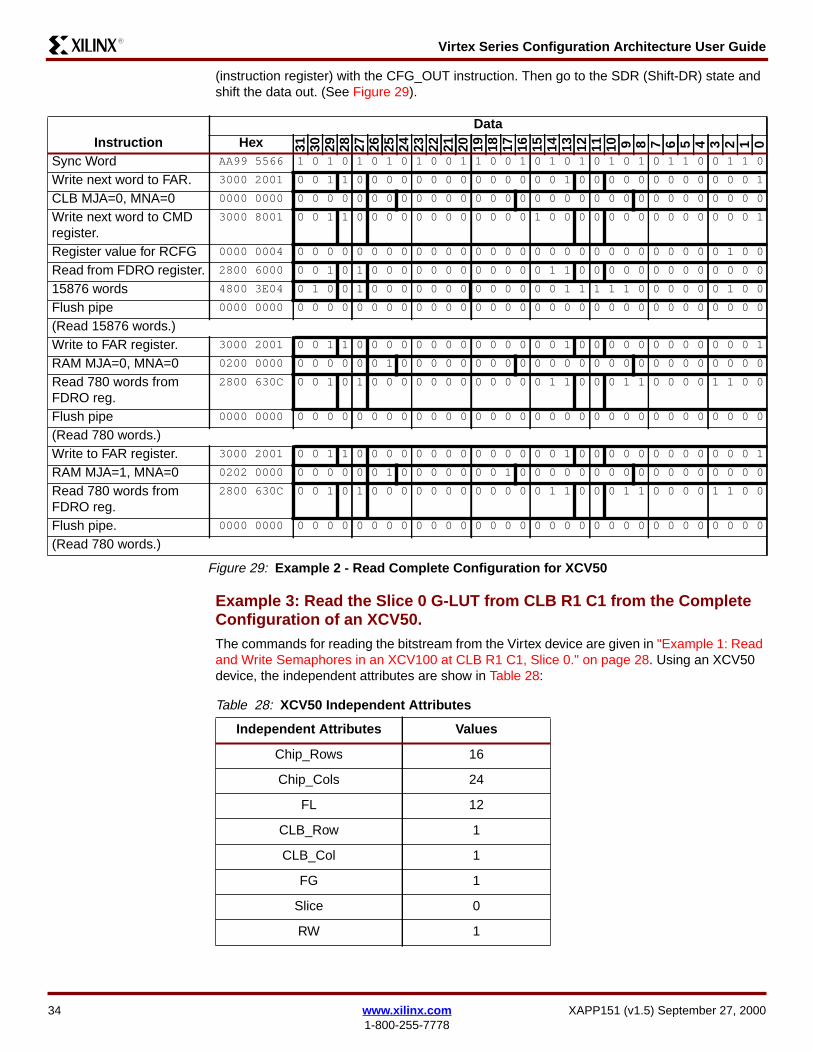
Virtex Series Configuration Architecture User GuideR13
(instruction register) with the CFG_OUT instruction Then go to the SDR (Shift-DR) state andshift the data out (See Figure 29)
Example 3 Read the Slice 0 G-LUT from CLB R1 C1 from the CompleteConfiguration of an XCV50The commands for reading the bitstream from the Virtex device are given in Example 1 Readand Write Semaphores in an XCV100 at CLB R1 C1 Slice 0 on page 28 Using an XCV50device the independent attributes are show in Table 28
InstructionData
Hex 31 30 29 28 27 26 25 24 23 22 21 20 19 18 17 16 15 14 13 12 11 10 9 8 7 6 5 4 3 2 1 0
Sync Word AA99 5566 1 0 1 0 1 0 1 0 1 0 0 1 1 0 0 1 0 1 0 1 0 1 0 1 0 1 1 0 0 1 1 0
Write next word to FAR 3000 2001 0 0 1 1 0 0 0 0 0 0 0 0 0 0 0 0 0 0 1 0 0 0 0 0 0 0 0 0 0 0 0 1
CLB MJA=0 MNA=0 0000 0000 0 0 0 0 0 0 0 0 0 0 0 0 0 0 0 0 0 0 0 0 0 0 0 0 0 0 0 0 0 0 0 0
Write next word to CMDregister
3000 8001 0 0 1 1 0 0 0 0 0 0 0 0 0 0 0 0 1 0 0 0 0 0 0 0 0 0 0 0 0 0 0 1
Register value for RCFG 0000 0004 0 0 0 0 0 0 0 0 0 0 0 0 0 0 0 0 0 0 0 0 0 0 0 0 0 0 0 0 0 1 0 0
Read from FDRO register 2800 6000 0 0 1 0 1 0 0 0 0 0 0 0 0 0 0 0 0 1 1 0 0 0 0 0 0 0 0 0 0 0 0 0
15876 words 4800 3E04 0 1 0 0 1 0 0 0 0 0 0 0 0 0 0 0 0 0 1 1 1 1 1 0 0 0 0 0 0 1 0 0
Flush pipe 0000 0000 0 0 0 0 0 0 0 0 0 0 0 0 0 0 0 0 0 0 0 0 0 0 0 0 0 0 0 0 0 0 0 0
(Read 15876 words)Write to FAR register 3000 2001 0 0 1 1 0 0 0 0 0 0 0 0 0 0 0 0 0 0 1 0 0 0 0 0 0 0 0 0 0 0 0 1
RAM MJA=0 MNA=0 0200 0000 0 0 0 0 0 0 1 0 0 0 0 0 0 0 0 0 0 0 0 0 0 0 0 0 0 0 0 0 0 0 0 0
Read 780 words fromFDRO reg
2800 630C 0 0 1 0 1 0 0 0 0 0 0 0 0 0 0 0 0 1 1 0 0 0 1 1 0 0 0 0 1 1 0 0
Flush pipe 0000 0000 0 0 0 0 0 0 0 0 0 0 0 0 0 0 0 0 0 0 0 0 0 0 0 0 0 0 0 0 0 0 0 0
(Read 780 words)Write to FAR register 3000 2001 0 0 1 1 0 0 0 0 0 0 0 0 0 0 0 0 0 0 1 0 0 0 0 0 0 0 0 0 0 0 0 1
RAM MJA=1 MNA=0 0202 0000 0 0 0 0 0 0 1 0 0 0 0 0 0 0 1 0 0 0 0 0 0 0 0 0 0 0 0 0 0 0 0 0
Read 780 words fromFDRO reg
2800 630C 0 0 1 0 1 0 0 0 0 0 0 0 0 0 0 0 0 1 1 0 0 0 1 1 0 0 0 0 1 1 0 0
Flush pipe 0000 0000 0 0 0 0 0 0 0 0 0 0 0 0 0 0 0 0 0 0 0 0 0 0 0 0 0 0 0 0 0 0 0 0
(Read 780 words)
Figure 29 Example 2 - Read Complete Configuration for XCV50
Table 28 XCV50 Independent Attributes
Independent Attributes Values
Chip_Rows 16
Chip_Cols 24
FL 12
CLB_Row 1
CLB_Col 1
FG 1
Slice 0
RW 1
34 wwwxilinxcom XAPP151 (v15) September 27 20001-800-255-7778
Virtex Series Configuration Architecture User GuideR13
From the equations given earlier in Table 7 calculating the range of values for fm_st_wdindicates that the word 13740 of the configuration is the starting word of the 12-word (FL=12)frame containing bit 0 of the G-LUT in Slice 0 of CLB R1C1 (Table 29)
The configuration bits for the given frame are as follows G-LUT[0] is in fm_wd=0 at bit 11
All 16 LUT SelectRAM bits are in the following words at the same bit index 11
Table 29 Variables Equations and Values for Slice 0 G-LUT
Variables Equations Values
MJA 1 le 242 rArr 24 ndash 1times 2 + 2 24
MNA 0 times (hellip) + lut_bit + 32 0 321 332 343 35
4 365 376 387 39
8 409 41
10 4211 43
12 4413 4514 4615 47
fm_bit_idx 3 + 18 times 1 ndash1 + RW times 32 52
fm_st_wd 12 times (8+ (24 ndash1) times 48 + [3247]) +1 x 12= 12 times (1112 + [3247]) +12= 13356 + 12 times 3247]
1374013920
fm_wd floor(5232) 1
fm_wd_bit_idx 31 + 32 ndash 52 11
BitstreamWord
Frame 32-bit Word FrameWord31 30 29 28 27 26 25 24 23 22 21 20 19 18 17 16 15 14 13 12 11 10 9 8 7 6 5 4 3 2 1 0
13740 0 0 0 0 0 0 0 0 0 0 0 0 0 0 0 0 0 0 0 0 0 0 0 0 0 0 0 0 0 0 0 0 013741 0 0 1 0 1 0 0 0 0 0 0 0 0 1 0 1 0 1 0 0 1 1 1 0 0 0 0 0 0 0 0 0 113742 1 0 1 1 0 0 1 1 0 0 0 0 0 0 0 0 0 0 1 0 1 1 0 0 1 1 0 0 0 0 0 0 213743 0 0 0 0 1 0 1 1 0 0 1 1 0 0 0 0 0 0 0 0 0 0 1 0 1 1 0 0 1 1 0 0 313744 0 0 0 0 0 0 0 0 1 0 1 1 0 0 1 1 0 0 0 0 0 0 0 0 0 0 1 0 1 1 0 0 413745 1 1 0 0 0 0 0 0 0 0 0 0 1 0 1 1 0 0 1 1 0 0 0 0 0 0 0 0 0 0 1 0 513746 1 1 0 0 1 1 0 0 0 0 0 0 0 0 0 0 1 0 1 1 0 0 1 1 0 0 0 0 0 0 0 0 613747 0 0 1 0 1 1 0 0 1 1 0 0 0 0 0 0 0 0 0 0 1 0 1 1 0 0 1 1 0 0 0 0 713748 0 0 0 0 0 0 1 0 1 1 0 0 1 1 0 0 0 0 0 0 0 0 0 0 1 0 1 1 0 0 1 1 813749 0 0 0 0 0 0 0 0 0 0 1 0 1 1 0 0 1 1 0 0 0 0 0 0 0 0 0 0 1 0 1 1 913750 0 0 1 1 0 0 0 0 0 0 0 0 0 0 1 0 1 1 0 0 1 0 1 0 0 0 0 0 0 0 0 0 1013751 0 1 0 1 0 0 0 0 0 0 0 0 0 0 0 0 0 0 0 0 0 0 0 0 0 0 0 0 0 0 0 0 11
Figure 30 Configuration Bits for Slice 0 CLB R1C1 G-LUT [0]
XAPP151 (v15) September 27 2000 wwwxilinxcom 351-800-255-7778
Virtex Series Configuration Architecture User GuideR13
The 16 bits are LUT[150]=0111111111111111 The LUT SelectRAM bits are inverted from theirlogic values The ldquologicalrdquo contents are LUT[150]=1000000000000000 Thus this G-LUTimplements a 4-input AND function
Example 4 Read the Slice 1 F-LUT from CLB R19 C16 from an XCV100Commands for reading the bitstream from the Virtex device are given in Figure 32 Use thefollowing independent attributes to find the given F-LUT
From the equations in Table 7 on page 11 calculating fm_st_wd indicates the starting wordwith respect to a configuration that starts at MJA=0 MNA=0 Because the frames we are
BitstreamWord
Frame 32-bit Word
LUT Bit31 30 29 28 27 26 25 24 23 22 21 20 19 18 17 16 15 14 13 12 11 10 9 8 7 6 5 4 3 2 1 0
13741 0 0 1 0 1 0 0 0 0 0 0 0 0 1 0 1 0 1 0 0 1 1 1 0 0 0 0 0 0 0 0 0 0
13753 1 0 1 0 0 0 0 0 0 0 0 0 0 0 0 1 0 0 0 1 1 1 0 0 0 0 0 0 0 0 0 0 1
13765 1 0 1 0 1 0 0 0 0 0 0 0 1 0 0 0 0 0 0 1 1 1 1 0 0 0 0 0 0 0 0 0 2
13777 0 0 0 0 1 0 0 0 0 0 0 1 1 1 0 1 1 0 1 0 1 1 0 0 0 0 0 0 0 0 0 0 3
13789 0 1 0 0 0 0 0 0 0 0 0 0 0 1 0 1 1 1 1 1 1 1 1 0 0 0 0 0 0 0 0 0 4
13801 1 0 1 0 1 0 0 0 0 0 0 1 0 0 0 1 1 0 0 1 1 1 0 0 0 0 0 0 0 0 0 0 5
13813 0 0 0 1 0 0 0 0 0 0 0 0 0 0 0 0 1 0 0 1 1 1 0 0 0 0 0 0 0 0 0 0 6
13825 0 1 1 0 1 0 0 0 0 0 0 1 0 1 0 0 1 1 0 0 1 1 0 0 0 0 0 0 0 0 0 0 7
13837 1 0 1 1 1 0 0 0 0 0 0 1 0 1 0 1 1 0 0 0 1 1 0 0 0 0 0 0 0 0 0 0 8
13849 1 0 0 0 0 0 0 0 0 0 0 0 0 0 0 0 1 1 1 0 1 1 0 0 0 0 0 0 0 0 0 0 9
13861 1 0 0 0 0 0 0 0 0 0 0 1 0 0 0 0 1 1 1 1 1 1 1 0 0 0 0 0 0 0 0 0 10
13873 1 0 0 0 0 0 0 1 0 0 0 0 0 1 0 0 0 1 1 0 1 1 0 0 0 1 0 0 0 0 0 0 11
13885 1 0 0 0 0 0 0 0 0 0 0 0 0 1 0 1 0 0 1 0 1 1 0 0 0 0 0 0 0 0 0 0 12
13897 0 0 0 0 1 0 0 0 0 0 0 0 0 1 0 0 0 0 0 0 1 1 0 0 0 0 0 0 0 0 0 0 13
13909 1 0 0 0 0 0 0 0 0 0 0 0 1 1 0 1 0 1 1 0 1 1 0 0 0 0 0 0 0 0 0 0 14
13921 1 0 1 0 0 0 0 0 0 0 0 1 1 1 0 1 1 1 1 1 0 1 0 0 0 0 0 0 0 0 0 0 15
Figure 31 Location of all 16 LUT SelectRAM Bits
Table 30 Virtex Bitstream Command Attributes
Independent Attributes Values
Chip_Rows 20
Chip_Cols 30
FL 14
CLB_Row 19
CLB_Col 16
FG 0
Slice 1
RW 1
36 wwwxilinxcom XAPP151 (v15) September 27 20001-800-255-7778
Virtex Series Configuration Architecture User GuideR13
interested in start at MJA=1 MNA=0 which is fm_st_wd = 126 so the first 126 words are notneeded (0ndash125) Therefore to find the given Slice 1 F-LUT see Table 31
Sixteen frames need to be read one for each bit in the LUT SelectRAM The bits in LUTSelectRAMs in Slice 1 occur in the opposite order that they do for Slice 0 LUT SelectRAMs
Frames are read sequentially with ascending addresses If read in LUT bit order LUT[0]LUT[1] hellip LUT[15] These are stored in descending addresses which require 16 separateread operations each reading one data frame and one pad frame However if read inascending address order LUT[15] LUT[14] hellip LUT[0] all 16 data frames are read with asingle read operation This requires only one pad frame for all 16 frames Thus it takes lesstime to read ascending frames starting at MJA=1 MNA=0 and finishing with frame MJA=1MNA=15 The frames in the XCV100 contain 14 32-bit words and a single pad wordCommands for reading only the F-LUT data are given in Figure 32
Table 31 Variables Equations and Values for Slice 1 F-LUT
Variables Equations Values
MJA 16 gt 302 rArr 2times16 ndash 30 ndash1 1
MNA lut_bit + 32 ndash Slice times (2 times lut_bit +17)= [015] + 32 ndash (2 times [015] + 17)= 15 ndash [015]
0 151 142 133 12
4 115 106 97 8
8 79 6
10 511 4
12 313 214 115 0
fm_bit_idx 3 + 18 times 19 ndash 0+ 32 377
fm_st_wd 14 times (8 + (1ndash 1) times 48 + [150]) +1 times 14= 14 times (8 + [150]) +14= 126 + 14 times [150]
= 336126
fm_wd floor(37732) 11
fm_wd_bit_idx 31 + 32 times 11 ndash 377 6
XAPP151 (v15) September 27 2000 wwwxilinxcom 371-800-255-7778
Virtex Series Configuration Architecture User GuideR13
The 377th bit of each frame is the bit in the F-LUT This LUT SelectRAM bit is in the framersquosword index 11 bit index 6
The configuration bits for the given frame in Figure 33 are as follows LUT Bit 15 is in MJA=1MNA=0 fm_wd=11 at bit 6
LUT bit 0 is in MJA=1 MNA=15 fm_wd=11 at bit 6
InstructionData
Hex 31 30 29 28 27 26 25 24 23 22 21 20 19 18 17 16 15 14 13 12 11 10 9 8 7 6 5 4 3 2 1 0
Sync Word AA99 5566 1 0 1 0 1 0 1 0 1 0 0 1 1 0 0 1 0 1 0 1 0 1 0 1 0 1 1 0 0 1 1 0
Write next (1) word to FAR 3000 2001 0 0 1 1 0 0 0 0 0 0 0 0 0 0 0 0 0 0 1 0 0 0 0 0 0 0 0 0 0 0 0 1
CLB MJA = 1 MNA = 0 0002 0000 0 0 0 0 0 0 0 0 0 0 0 0 0 0 1 0 0 0 0 0 0 0 0 0 0 0 0 0 0 0 0 0
Write next word to CMD 3000 8001 0 0 1 1 0 0 0 0 0 0 0 0 0 0 0 0 1 0 0 0 0 0 0 0 0 0 0 0 0 0 0 1
Register value for RCFG 0000 0004 0 0 0 0 0 0 0 0 0 0 0 0 0 0 0 0 0 0 0 0 0 0 0 0 0 0 0 0 0 1 0 0
Read from FDRO 2800 60EE 0 0 1 0 1 0 0 0 0 0 0 0 0 0 0 0 0 1 1 0 0 0 0 0 1 1 1 0 1 1 1 0
Flush pipe 0000 0000 0 0 0 0 0 0 0 0 0 0 0 0 0 0 0 0 0 0 0 0 0 0 0 0 0 0 0 0 0 0 0 0
(Read 238 words)
Figure 32 Commands to read Slice 1 F-LUT
Frame WordFrame 32-bit Word
31 30 29 28 27 26 25 24 23 22 21 20 19 18 17 16 15 14 13 12 11 10 9 8 7 6 5 4 3 2 1 0
0 0 0 0 0 0 0 0 0 0 0 0 0 0 0 0 0 0 0 0 0 0 0 0 0 0 0 0 0 0 0 0 0
1 1 1 0 0 0 0 0 0 0 0 0 0 0 1 0 1 1 1 1 1 1 1 0 0 0 0 0 0 0 0 0 0
2 1 1 1 1 1 1 1 1 0 0 0 0 0 0 0 0 0 0 1 1 1 1 1 1 1 1 0 0 0 0 0 0
3 0 0 0 0 1 1 1 1 1 1 1 1 0 0 0 0 0 0 0 0 0 0 1 1 1 1 1 1 1 1 0 0
4 0 0 0 0 0 0 0 0 1 1 1 1 1 1 1 1 0 0 0 0 0 0 0 0 0 0 1 1 1 1 1 1
5 1 1 0 0 0 0 0 0 0 0 0 0 1 1 1 1 1 1 1 1 0 0 0 0 0 0 0 0 0 0 1 1
6 1 1 1 1 1 1 0 0 0 0 0 0 0 0 0 0 1 1 1 1 1 1 1 1 0 0 0 0 0 0 0 0
7 0 0 1 1 1 1 1 1 1 1 0 0 0 0 0 0 0 0 0 0 1 1 1 1 1 1 1 1 0 0 0 0
8 0 0 0 0 0 0 1 1 1 1 1 1 1 1 0 0 0 0 0 0 0 0 0 0 1 1 1 1 1 1 1 1
9 0 0 0 0 0 0 0 0 0 0 1 1 1 1 1 1 1 1 0 0 0 0 0 0 0 0 0 0 1 1 1 1
10 1 1 1 1 0 0 0 0 0 0 0 0 0 0 1 1 1 1 1 1 1 1 0 0 0 0 0 0 0 0 0 0
11 1 1 1 1 1 1 1 1 0 0 0 0 0 0 0 0 0 0 1 1 1 1 1 1 1 0 0 0 0 0 0 0
12 0 0 0 0 1 1 1 1 1 1 1 1 0 0 0 0 0 0 0 0 0 0 1 1 1 1 1 1 0 0 0 0
13 0 0 0 0 0 0 0 0 0 1 1 1 0 0 0 0 0 0 0 0 0 0 1 1 1 1 1 1 0 0 0 0
Figure 33 Frame Containing F-LUT[15]
Bit streamWord
Frame 32-bit WordFmWd31 30 29 28 27 26 25 24 23 22 21 20 19 18 17 16 15 14 13 12 11 10 9 8 7 6 5 4 3 2 1 0
336 0 0 0 0 0 0 0 0 0 0 0 0 0 0 0 0 0 0 0 0 0 0 0 0 0 0 0 0 0 0 0 0 0337 0 1 0 0 1 0 0 0 0 0 0 1 0 1 0 0 1 1 0 0 1 1 0 0 0 0 0 0 0 0 0 0 1338 1 0 1 1 0 0 1 1 0 0 0 0 0 0 0 0 0 0 1 0 1 1 0 0 1 1 0 0 0 0 0 0 2339 0 0 0 0 1 0 1 1 0 0 1 1 0 0 0 0 0 0 0 0 0 0 1 0 1 1 0 0 1 1 0 0 3340 0 0 0 0 0 0 0 0 1 0 1 1 0 0 1 1 0 0 0 0 0 0 0 0 0 0 1 0 1 1 0 0 4341 1 1 0 0 0 0 0 0 0 0 0 0 1 0 1 1 0 0 1 1 0 0 0 0 0 0 0 0 0 0 1 0 5342 1 1 0 0 1 1 0 0 0 0 0 0 0 0 0 0 1 0 1 1 0 0 1 1 0 0 0 0 0 0 0 0 6343 0 0 1 0 1 1 0 0 1 1 0 0 0 0 0 0 0 0 0 0 1 0 1 1 0 0 1 1 0 0 0 0 7
Figure 34 Frame Containing F-LUT [0]
38 wwwxilinxcom XAPP151 (v15) September 27 20001-800-255-7778
Virtex Series Configuration Architecture User GuideR13
For the sake of brevity here are the sixteen 11th words in the order they appear in thebitstream
The bits are LUT[150]=0111111111111111 The LUT SelectRAM bits are inverted from thelogic sense The logical contents are LUT[150]=1000000000000000 Thus this F-LUTimplements a 4-input AND gate
Example 5 Read All Bits in Slice 0 G-LUTs from CLB C2 and XCV50Given the following attributes the necessary values to find the G-LUT data can be computed
344 0 0 0 0 0 0 1 0 1 1 0 0 1 1 0 0 0 0 0 0 0 0 0 0 1 0 1 1 0 0 1 1 8345 0 0 0 0 0 0 0 0 0 0 1 0 1 1 0 0 1 1 0 0 0 0 0 0 0 0 0 0 1 0 1 1 9346 0 0 1 1 0 0 0 0 0 0 0 0 0 0 1 0 1 1 0 0 1 1 0 0 0 0 0 0 0 0 0 0 10347 1 1 1 1 1 0 1 1 0 0 0 0 0 0 0 0 0 0 1 0 1 1 1 0 1 1 0 1 0 0 0 0 11348 0 0 0 0 1 1 1 0 1 0 1 1 0 0 0 0 0 0 0 0 0 0 1 1 1 1 0 1 0 0 0 0 12349 0 0 0 0 0 1 0 0 0 0 1 0 0 0 0 0 0 0 0 0 0 0 0 0 0 0 0 0 0 0 0 0 13
Bit streamWord
Frame 32-bit WordFmWd31 30 29 28 27 26 25 24 23 22 21 20 19 18 17 16 15 14 13 12 11 10 9 8 7 6 5 4 3 2 1 0
Figure 34 Frame Containing F-LUT [0]
BitstreamWord
Frame 32-bit WordLUT Bit31 30 29 28 27 26 25 24 23 22 21 20 19 18 17 16 15 14 13 12 11 10 9 8 7 6 5 4 3 2 1 0
137 1 1 1 1 1 1 1 1 0 0 0 0 0 0 0 0 0 0 1 1 1 1 1 1 1 0 0 0 0 0 0 0 15151 1 0 1 1 1 0 1 1 0 0 0 0 0 0 0 0 0 0 1 0 1 1 1 0 1 1 0 0 0 0 0 0 14165 1 0 1 1 0 0 1 1 0 0 0 0 0 0 0 0 0 0 1 0 1 1 1 0 1 1 0 0 0 0 0 0 13179 1 0 1 1 1 0 1 1 0 0 0 0 0 0 0 0 0 0 1 0 1 1 1 0 1 1 0 0 0 0 0 0 12193 1 1 1 1 1 0 1 1 0 0 0 0 0 0 0 0 0 0 1 1 1 1 1 0 1 1 0 0 0 0 0 0 11207 1 1 1 1 1 1 1 1 0 0 0 0 0 0 0 0 0 0 1 1 1 1 1 1 1 1 1 0 1 0 0 0 10221 1 1 1 1 1 0 1 1 0 0 0 0 0 0 0 0 0 0 1 1 1 1 1 0 1 1 0 0 0 0 0 0 9235 1 0 1 1 1 0 1 1 0 0 0 0 0 0 0 0 0 0 1 0 1 1 1 0 1 1 0 0 0 0 0 0 8249 1 0 1 1 0 0 1 1 0 0 0 0 0 0 0 0 0 0 1 0 1 1 0 0 1 1 0 0 0 0 0 0 7263 1 0 1 1 0 1 1 1 1 0 0 0 0 0 0 0 0 0 1 0 1 1 0 1 1 1 0 0 0 0 0 0 6277 1 1 1 1 0 0 1 1 0 0 0 0 0 0 0 0 0 0 1 1 1 1 0 0 1 1 0 0 0 0 0 0 5291 1 1 1 1 1 1 1 1 0 0 0 0 0 0 0 0 0 0 1 1 1 1 1 1 1 1 0 0 0 0 0 0 4305 1 1 1 1 1 0 1 1 0 0 0 0 0 0 0 0 0 0 1 1 1 1 1 0 1 1 0 0 0 0 0 0 3319 1 0 1 1 0 1 1 1 0 0 0 0 0 0 0 0 0 0 1 0 1 1 0 1 1 1 0 0 0 0 0 0 2333 1 0 1 1 0 0 1 1 0 0 0 0 0 0 0 0 0 0 1 0 1 1 0 0 1 1 0 0 0 0 0 0 1347 1 1 1 1 1 0 1 1 0 0 0 0 0 0 0 0 0 0 1 0 1 1 1 0 1 1 0 1 0 0 0 0 0
Figure 35 Sixteen Words Containing the F-LUT bit
Table 32 All Bits Slice 0 GndashLUTs from CLB C2 and XCV50
Independent Attributes Values
Chip_Rows 16
Chip_Cols 24
FL 12
CLB_Row 116
CLB_Col 2
XAPP151 (v15) September 27 2000 wwwxilinxcom 391-800-255-7778
Virtex Series Configuration Architecture User GuideR13
From the equations in Table 7 the dependent variables can be calculated
Note that fm_bit_idx fm_wd and fm_wd_bit_idx have 16 values one for each row on theXCV50 Figure 37 shows where the data lies in the first frame which contains G[0] for the entirecolumn The process is the same for the other 15 frames The commands for reading the LUTSelectRAM data are given in Figure 36
From the calculation for fm_st_wd Frame 0 would start at word 12588 reading the wholeconfiguration The instructions in Figure 36 start at that word so word 0 (ignoring the 12 wordsin the pad frame) is the same as word 12588 of the entire CLB configuration The 12 words inthe frame are shown in Figure 37
FG 1
Slice 0
lut_bit 015
RW 1
Table 32 All Bits Slice 0 GndashLUTs from CLB C2 and XCV50 (Continued)
Independent Attributes Values
Table 33 Dependent Variables Equations and Values
Variables Equations Values
MJA 2 le 242 rArr 24 ndash 2times 2 + 2 22
MNAlut_bit + 32 ndash Slice times (2 times lut_bit + 17)= lut_bit + 32 ndash 0 times (2 times lut_bit + 17)= [015] + 32
032 436 840 1244
133 537 941 1345
234 638 1042 1456
335 739 1143 1547
fm_bit_idx3 + 18 times CLB_Row ndash 1+ 32 = 34 + 18 times[116]
152 5124 9196 13268
270 6142 10214 14286
388 7160 11232 15304
4106 8178 12250 16322
fm_st_wd12 times (8 + (22 ndash1) times 48 + MNA) + 1 times 12= 12 times (1016 + MNA) + 12= 12204 + 12 times MNA
0 12588 4 12636 8 12684 12 12732
1 12600 5 12648 9 12696 13 12744
2 12612 6 12660 10 12708 14 12756
3 12624 7 12672 11 12720 15 12768
fm_wd floor (fm_bit_idx32)
11 53 96 138
22 64 106 148
32 75 117 159
43 85 127 1610
fm_wd_bit_idx 31 + 32 times fm_wd ndash fm_bit_idx
111 53 927 1319
225 617 109 141
37 7 31 1123 1515
421 813 125 1629
40 wwwxilinxcom XAPP151 (v15) September 27 20001-800-255-7778
Virtex Series Configuration Architecture User GuideR13
The LUT SelectRAM bits have been shaded for ease of identification It can be seen from thecalculation of fm_bit_idx that the LUT SelectRAM bits are in the order 116 For example fromthe above calculations for fm_wd and fm_wd_bit_idx G-LUT[0] in R1C2 is in fm_wd 1fm_wd_bit_idx 11 This bit is the shaded bit in word 1 at bit index 11 Similarly the G-LUT[0] forthe other 15 CLB rows are also shaded in this table
Example 6 Read Block SelectRAM index 387 of RAM R2 C0 from anXCV100ECommands for reading the bitstream from the Virtex device are given in Figure 38 Use thefollowing independent attributes to find the given F-LUT
InstructionData
Hex 31 30 29 28 27 26 25 24 23 22 21 20 19 18 17 16 15 14 13 12 11 10 9 8 7 6 5 4 3 2 1 0
Sync Word AA99 5566 1 0 1 0 1 0 1 0 1 0 0 1 1 0 0 1 0 1 0 1 0 1 0 1 0 1 1 0 0 1 1 0
Write next (1) word to FAR 3000 2001 0 0 1 1 0 0 0 0 0 0 0 0 0 0 0 0 0 0 1 0 0 0 0 0 0 0 0 0 0 0 0 1
CLB MJA=22 MNA=32 002C 4000 0 0 0 0 0 0 0 0 0 0 1 0 1 1 0 0 0 1 0 0 0 0 0 0 0 0 0 0 0 0 0 0
Write next word to CMD 3000 8001 0 0 1 1 0 0 0 0 0 0 0 0 0 0 0 0 1 0 0 0 0 0 0 0 0 0 0 0 0 0 0 1
Register value for RCFG 0000 0004 0 0 0 0 0 0 0 0 0 0 0 0 0 0 0 0 0 0 0 0 0 0 0 0 0 0 0 0 0 1 0 0
Read from FDRO 2800 60CC 0 0 1 0 1 0 0 0 0 0 0 0 0 0 0 0 0 1 1 0 0 0 0 0 1 1 0 0 1 1 0 0
Flush pipe 0000 0000 0 0 0 0 0 0 0 0 0 0 0 0 0 0 0 0 0 0 0 0 0 0 0 0 0 0 0 0 0 0 0 0
(Read 204 words)
Figure 36 Commands to read RC2S0 G-LUT
WordFrame 32-bit Word
CLB Row31 30 29 28 27 26 25 24 23 22 21 20 19 18 17 16 15 14 13 12 11 10 9 8 7 6 5 4 3 2 1 0
0 0 0 0 0 0 0 0 0 0 0 0 0 0 0 0 0 0 0 0 0 0 0 0 0 0 0 0 0 0 0 0 0
1 0 0 0 0 1 0 0 0 0 0 0 0 0 1 0 1 0 1 0 0 1 1 0 0 0 0 0 0 0 0 0 0 12 1 0 1 1 0 0 1 1 0 0 0 0 0 0 0 0 0 0 1 0 1 1 0 0 1 1 0 0 0 0 0 0 2 33 0 0 0 0 1 0 1 1 0 0 1 1 0 0 0 0 0 0 0 0 0 0 1 0 1 1 0 0 1 1 0 0 4 54 0 0 0 0 0 0 0 0 1 0 1 1 0 0 1 1 0 0 0 0 0 0 0 0 0 0 1 0 1 1 0 0 65 1 1 0 0 0 0 0 0 0 0 0 0 1 0 1 1 0 0 1 1 0 0 0 0 0 0 0 0 0 0 1 0 7 86 1 1 0 0 1 1 0 0 0 0 0 0 0 0 0 0 1 0 1 1 0 0 1 1 0 0 0 0 0 0 0 0 9 107 0 0 1 0 1 1 0 0 1 1 0 0 0 0 0 0 0 0 0 0 1 0 1 1 0 0 1 1 0 0 0 0 11 128 0 0 0 0 0 0 1 0 1 1 0 0 1 1 0 0 0 0 0 0 0 0 0 0 1 0 1 1 0 0 1 1 13 149 0 0 0 0 0 0 0 0 0 0 1 0 1 1 0 0 1 1 0 0 0 0 0 0 0 0 0 0 1 0 1 1 15
10 0 0 1 1 0 0 0 0 0 0 0 0 0 0 1 0 1 1 0 0 1 0 1 0 0 0 0 0 0 0 0 0 1611 0 1 0 1 0 0 0 0 0 0 0 0 0 0 0 0 0 0 0 0 0 0 0 0 0 0 0 0 0 0 0 0
Figure 37 Frame for RC2S0 G-LUTs Bit G[0]
Table 34 Virtex Bitstream Command Attributes
Independent Attributes Values
Chip_Rams 4
FL 14
RAM_Row 2
RAM_Col 0
ram_bit 387
RW 1
XAPP151 (v15) September 27 2000 wwwxilinxcom 411-800-255-7778
Virtex Series Configuration Architecture User GuideR13
Since we are attempting to read only one bit location only one frame is necessary to be readWe use the equations of Table 15 Table 16 and Table 17 to determine the dependentvariables
Commands for reading this memory index are given in Figure 38
RAM bit 387 is at fm_wd=6 bit 4
Table 35 Variables Equations and Values for Slice 1 F-LUT
Variables Equations Values
MJA_virtex 0 lt42 rArr 2times(42 -1 -0) 2
MJA_adj 0 lt42 rArr 2 2
MJA MJA_virtex + MJA_adj 4
MNA floor(((38764)64)32)+ 2 x floor(((38764)32)16)+ 4 x floor(((38764)16)8) + 8 x floor(((38764)8)4)+ 16 x floor(((38764)4)2) + 32 x floor(((38764)2)1)
24
fm_bit_idx 3 + 18 times 19 ndash 0 + 32 219
fm_st_wd 14 x 24 + 1 x 14 350
fm_wd floor(21932) 6
fm_wd_bit_idx 31 + 32 times 6 ndash 219 4
InstructionData
Hex 31 30 29 28 27 26 25 24 23 22 21 20 19 18 17 16 15 14 13 12 11 10 9 8 7 6 5 4 3 2 1 0
Sync Word AA99 5566 1 0 1 0 1 0 1 0 1 0 0 1 1 0 0 1 0 1 0 1 0 1 0 1 0 1 1 0 0 1 1 0
Write next (1) word to FAR 3000 2001 0 0 1 1 0 0 0 0 0 0 0 0 0 0 0 0 0 0 1 0 0 0 0 0 0 0 0 0 0 0 0 1
CLB MJA = 4 MNA = 24 0208 3000 0 0 0 0 0 0 1 0 0 0 0 0 1 0 0 0 0 0 1 1 0 0 0 0 0 0 0 0 0 0 0 0
Write next word to CMD 3000 8001 0 0 1 1 0 0 0 0 0 0 0 0 0 0 0 0 1 0 0 0 0 0 0 0 0 0 0 0 0 0 0 1
Register value for RCFG 0000 0004 0 0 0 0 0 0 0 0 0 0 0 0 0 0 0 0 0 0 0 0 0 0 0 0 0 0 0 0 0 1 0 0
Read from FDRO 2800 601C 0 0 1 0 1 0 0 0 0 0 0 0 0 0 0 0 0 1 1 0 0 0 0 0 0 0 0 1 1 1 0 0
Flush pipe 0000 0000 0 0 0 0 0 0 0 0 0 0 0 0 0 0 0 0 0 0 0 0 0 0 0 0 0 0 0 0 0 0 0 0
(Read 28 words)
Figure 38 Commands to read Block SelectRAM index 387
42 wwwxilinxcom XAPP151 (v15) September 27 20001-800-255-7778
Virtex Series Configuration Architecture User GuideR13
Glossary Block SelectRAM Resource
One of several large fully-synchronous dual-port memories in the Virtex FPGAs Each ofthese memories contain 4096 bits The organization of each memory is configurable Theblock SelectRAM resource complements the smaller distributed LUT SelectRAMs
Boundary Scan Interface
One of the configuration interfaces on the Virtex device This is a bit-serial interface TheBoundary Scan interface is also known as the JTAG port Also see the SelectMAP interface
Capture Data
The flip-flop and pad data saved from the logic cells and IO blocks into the bitstream Use theCAPTURE_VIRTEX primitive in your HDL code to specify the trigger and clock for the captureoperation
Configurable Logic Block (CLB)
The functional elements for constructing logic circuits The Virtex CLB is made up of Sliceswhich contain Logic Cells
Configuration Bitstream
Configuration commands optionally with configuration data
Configuration Commands
Instructions for the Virtex device There are two classes of Configuration Command mdash Majorand Minor The Major Commands read and write data to configuration registers in the Virtexdevice The Minor commands instruct the Virtex configuration logic to perform specificfunctions See Command Register (CMD) on page 18
Configuration Data
Bits that directly define the state of programmable logic These are written to a Virtex device ina configuration bitstream and read as Readback Data from a Virtex device
Frame WordFrame 32-bit Word
31 30 29 28 27 26 25 24 23 22 21 20 19 18 17 16 15 14 13 12 11 10 9 8 7 6 5 4 3 2 1 0
0 0 0 0 0 0 0 0 0 0 0 0 0 0 0 0 0 0 0 0 0 0 0 0 0 0 0 0 0 0 0 0 0
1 1 1 0 0 0 0 0 0 0 0 0 0 0 1 0 1 1 1 1 1 1 1 0 0 0 0 0 0 0 0 0 0
2 1 1 1 1 1 1 1 1 0 0 0 0 0 0 0 0 0 0 1 1 1 1 1 1 1 1 0 0 0 0 0 0
3 0 0 0 0 1 1 1 1 1 1 1 1 0 0 0 0 0 0 0 0 0 0 1 1 1 1 1 1 1 1 0 0
4 0 0 0 0 0 0 0 0 1 1 1 1 1 1 1 1 0 0 0 0 0 0 0 0 0 0 1 1 1 1 1 1
5 1 1 0 0 0 0 0 0 0 0 0 0 1 1 1 1 1 1 1 1 0 0 0 0 0 0 0 0 0 0 1 1
6 1 1 1 1 1 1 0 0 0 0 0 0 0 0 0 0 1 1 1 1 1 1 1 1 0 0 0 0 0 0 0 0
7 0 0 1 1 1 1 1 1 1 1 0 0 0 0 0 0 0 0 0 0 1 1 1 1 1 1 1 1 0 0 0 0
8 0 0 0 0 0 0 1 1 1 1 1 1 1 1 0 0 0 0 0 0 0 0 0 0 1 1 1 1 1 1 1 1
9 0 0 0 0 0 0 0 0 0 0 1 1 1 1 1 1 1 1 0 0 0 0 0 0 0 0 0 0 1 1 1 1
10 1 1 1 1 0 0 0 0 0 0 0 0 0 0 1 1 1 1 1 1 1 1 0 0 0 0 0 0 0 0 0 0
11 1 1 1 1 1 1 1 1 0 0 0 0 0 0 0 0 0 0 1 1 1 1 1 1 1 0 0 0 0 0 0 0
12 0 0 0 0 1 1 1 1 1 1 1 1 0 0 0 0 0 0 0 0 0 0 1 1 1 1 1 1 0 0 0 0
13 0 0 0 0 0 0 0 0 0 1 1 1 0 0 0 0 0 0 0 0 0 0 1 1 1 1 1 1 0 0 0 0
Figure 39 Frame MNA=24
XAPP151 (v15) September 27 2000 wwwxilinxcom 431-800-255-7778
Virtex Series Configuration Architecture User GuideR13
Configuration Frame
The configuration bits in a Virtex device are organized in columns A column of CLBs with theIO blocks above and below the CLBs contain 48 frames of configuration bits The smallestnumber of bits that can be read or written through the configuration interfaces is one frame
Configuration Interface
A logical interface on the Virtex device through which configuration commands and data can beread and written A interface consists of one or more physical Device Pins
Configuration Readback
The operation of reading Configuration Data (also known as Readback Data) from a Virtexdevice
Device Pin
One of the electrical connections on the package containing the Virtex device
Frame
See Configuration Frame
Logic Cell (LC)
The basic building block of the Virtex CLB An LC includes a 4-input function generator carrylogic and a storage element
LUT SelectRAMs
Shallow RAM structures implemented in CLB Lookup Tables (LUTs) See also blockSelectRAM section
Pad
Pad bits are extra bits used to make the total number of bits in a frame an integral multiple of32 the number of bits in a configuration word A Pad Word is an extra word used at the end ofa Configuration Frame for pipelining A Pad Frame is an extra Configuration Frame used at thebeginning of a Configuration Readback and at the end of a Configuration Write for pipelining
Readback Data
Configuration data read from a Virtex device The data is organized as Configuration Frames
SelectMAP Interface
One of the configuration interfaces on the Virtex device This is a byte-serial interface The pinsin the SelectMAP interface may be used as user IO after configuration has been completed orremain configured as a configuration interface
Slice
A subdivision of the Virtex CLB There are two vertical slices in a Virtex CLB Each slicecontains two Logic Cells
Sync Word
A 32-bit word with a value that is used to synchronize the configuration logic
44 wwwxilinxcom XAPP151 (v15) September 27 20001-800-255-7778
Virtex Series Configuration Architecture User GuideR13
RevisionHistory
The following table shows the revision history for this document
Date Version Revision
061799 10 Initial Release
072799 11 Updated the following tables Table 5 equation for MNA Table 7equations for MJA amp fm_bit_idx
092099 12 Changes in page 5 Most formulae in Table 7 have been revisedDocumented pad capture value P Corrected bit locations inExamples
022200 13 Updated to include Virtex-E block SelectRAM Correctedfm_bit_idx (Right IOB) equations in Table 12 and fm_st_wddefinition Corrected CRC algorithm Various corrections inExamples Reformatted and edited document and figures
080300 14 Updated to include Virtex-EM devices in Table 3 and Table 24
092700 15 Added Partial Reconfiguration of CLB section and Figure 26
XAPP151 (v15) September 27 2000 wwwxilinxcom 451-800-255-7778
- Summary
- Introduction
-
- CLBs IOBs and Configurations
-
- Configuring Virtex Devices
- Reading Configuration Bits From a Virtex Device
-
- Configuration Columns
- Configuration Addressing
-
- Block Type Major Address Minor Address
-
- Virtex Major Addresses
- Virtex-EM Major Addresses
- Virtex-E Major Addresses
-
- Frames
-
- Frame Sizes
- Frame Organization
- Location of LUT SelectRAM Bits
-
- Configuration Data Operations
-
- Reading Configuration Data
- Writing Configuration Data
- Altering Configuration Data
-
- Definitions
- CLB LUT SelectRAM Dependent Variables
-
- Virtex-E CLB LUT SelectRAM Dependent Variables
- LUT SelectRAM Examples
-
- CLB Flip-Flop Dependent Variables
-
- Virtex-E CLB Flip-Flop Dependent Variables
-
- IOB Dependent Variables
-
- Virtex-E IOB Dependent Variables
-
- Block SelectRAM Dependent Variables
-
- Virtex-E Block SelectRAM Dependent Variables
-
- Configuration Logic Basics
-
- Configuration Data
- Configuration Flow
-
- For Initial Configuration
- Reading Configuration
- Writing Configuration
-
- Configuration Registers
-
- Command Register (CMD)
- Configuration Option Register (COR)
- Control Register (CTL)
- Cyclic Redundancy Check (CRC)
-
- CRC Algorithm
-
- Frame Address Register (FAR)
- Frame Data Input Register (FDRI)
- Frame Data Output Register (FDRO)
- Frame Length Register (FLR)
- Legacy Output Register (LOUT)
- Mask Register (MASK)
- Status Register (STAT)
-
- Configuration Interface
- Partial Reconfiguration of CLBs
- Examples
-
- Example 1 Read and Write Semaphores in an XCV100 at CLB R1 C1 Slice 0
- Example 2 Reading the Complete Configuration from an XCV50
- Example 3 Read the Slice 0 G-LUT from CLB R1 C1 from the Complete Configuration of an XCV50
- Example 4 Read the Slice 1 F-LUT from CLB R19 C16 from an XCV100
- Example 5 Read All Bits in Slice 0 G-LUTs from CLB C2 and XCV50
- Example 6 Read Block SelectRAM index 387 of RAM R2 C0 from an XCV100E
-
- Glossary
-
- Block SelectRAM Resource
- Boundary Scan Interface
- Capture Data
- Configurable Logic Block (CLB)
- Configuration Bitstream
- Configuration Commands
- Configuration Data
- Configuration Frame
- Configuration Interface
- Configuration Readback
- Device Pin
- Frame
- Logic Cell (LC)
- LUT SelectRAMs
- Pad
- Readback Data
- SelectMAP Interface
- Slice
- Sync Word
-
- Revision History
-
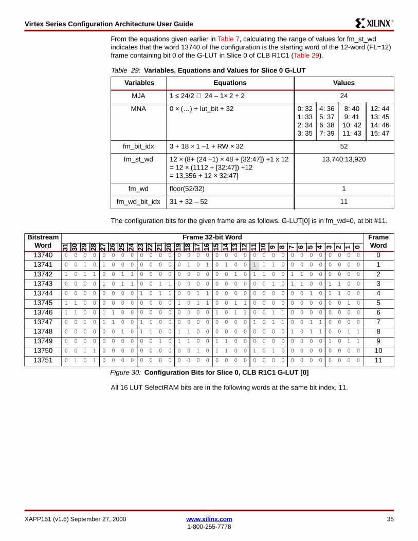
Virtex Series Configuration Architecture User GuideR13
From the equations given earlier in Table 7 calculating the range of values for fm_st_wdindicates that the word 13740 of the configuration is the starting word of the 12-word (FL=12)frame containing bit 0 of the G-LUT in Slice 0 of CLB R1C1 (Table 29)
The configuration bits for the given frame are as follows G-LUT[0] is in fm_wd=0 at bit 11
All 16 LUT SelectRAM bits are in the following words at the same bit index 11
Table 29 Variables Equations and Values for Slice 0 G-LUT
Variables Equations Values
MJA 1 le 242 rArr 24 ndash 1times 2 + 2 24
MNA 0 times (hellip) + lut_bit + 32 0 321 332 343 35
4 365 376 387 39
8 409 41
10 4211 43
12 4413 4514 4615 47
fm_bit_idx 3 + 18 times 1 ndash1 + RW times 32 52
fm_st_wd 12 times (8+ (24 ndash1) times 48 + [3247]) +1 x 12= 12 times (1112 + [3247]) +12= 13356 + 12 times 3247]
1374013920
fm_wd floor(5232) 1
fm_wd_bit_idx 31 + 32 ndash 52 11
BitstreamWord
Frame 32-bit Word FrameWord31 30 29 28 27 26 25 24 23 22 21 20 19 18 17 16 15 14 13 12 11 10 9 8 7 6 5 4 3 2 1 0
13740 0 0 0 0 0 0 0 0 0 0 0 0 0 0 0 0 0 0 0 0 0 0 0 0 0 0 0 0 0 0 0 0 013741 0 0 1 0 1 0 0 0 0 0 0 0 0 1 0 1 0 1 0 0 1 1 1 0 0 0 0 0 0 0 0 0 113742 1 0 1 1 0 0 1 1 0 0 0 0 0 0 0 0 0 0 1 0 1 1 0 0 1 1 0 0 0 0 0 0 213743 0 0 0 0 1 0 1 1 0 0 1 1 0 0 0 0 0 0 0 0 0 0 1 0 1 1 0 0 1 1 0 0 313744 0 0 0 0 0 0 0 0 1 0 1 1 0 0 1 1 0 0 0 0 0 0 0 0 0 0 1 0 1 1 0 0 413745 1 1 0 0 0 0 0 0 0 0 0 0 1 0 1 1 0 0 1 1 0 0 0 0 0 0 0 0 0 0 1 0 513746 1 1 0 0 1 1 0 0 0 0 0 0 0 0 0 0 1 0 1 1 0 0 1 1 0 0 0 0 0 0 0 0 613747 0 0 1 0 1 1 0 0 1 1 0 0 0 0 0 0 0 0 0 0 1 0 1 1 0 0 1 1 0 0 0 0 713748 0 0 0 0 0 0 1 0 1 1 0 0 1 1 0 0 0 0 0 0 0 0 0 0 1 0 1 1 0 0 1 1 813749 0 0 0 0 0 0 0 0 0 0 1 0 1 1 0 0 1 1 0 0 0 0 0 0 0 0 0 0 1 0 1 1 913750 0 0 1 1 0 0 0 0 0 0 0 0 0 0 1 0 1 1 0 0 1 0 1 0 0 0 0 0 0 0 0 0 1013751 0 1 0 1 0 0 0 0 0 0 0 0 0 0 0 0 0 0 0 0 0 0 0 0 0 0 0 0 0 0 0 0 11
Figure 30 Configuration Bits for Slice 0 CLB R1C1 G-LUT [0]
XAPP151 (v15) September 27 2000 wwwxilinxcom 351-800-255-7778
Virtex Series Configuration Architecture User GuideR13
The 16 bits are LUT[150]=0111111111111111 The LUT SelectRAM bits are inverted from theirlogic values The ldquologicalrdquo contents are LUT[150]=1000000000000000 Thus this G-LUTimplements a 4-input AND function
Example 4 Read the Slice 1 F-LUT from CLB R19 C16 from an XCV100Commands for reading the bitstream from the Virtex device are given in Figure 32 Use thefollowing independent attributes to find the given F-LUT
From the equations in Table 7 on page 11 calculating fm_st_wd indicates the starting wordwith respect to a configuration that starts at MJA=0 MNA=0 Because the frames we are
BitstreamWord
Frame 32-bit Word
LUT Bit31 30 29 28 27 26 25 24 23 22 21 20 19 18 17 16 15 14 13 12 11 10 9 8 7 6 5 4 3 2 1 0
13741 0 0 1 0 1 0 0 0 0 0 0 0 0 1 0 1 0 1 0 0 1 1 1 0 0 0 0 0 0 0 0 0 0
13753 1 0 1 0 0 0 0 0 0 0 0 0 0 0 0 1 0 0 0 1 1 1 0 0 0 0 0 0 0 0 0 0 1
13765 1 0 1 0 1 0 0 0 0 0 0 0 1 0 0 0 0 0 0 1 1 1 1 0 0 0 0 0 0 0 0 0 2
13777 0 0 0 0 1 0 0 0 0 0 0 1 1 1 0 1 1 0 1 0 1 1 0 0 0 0 0 0 0 0 0 0 3
13789 0 1 0 0 0 0 0 0 0 0 0 0 0 1 0 1 1 1 1 1 1 1 1 0 0 0 0 0 0 0 0 0 4
13801 1 0 1 0 1 0 0 0 0 0 0 1 0 0 0 1 1 0 0 1 1 1 0 0 0 0 0 0 0 0 0 0 5
13813 0 0 0 1 0 0 0 0 0 0 0 0 0 0 0 0 1 0 0 1 1 1 0 0 0 0 0 0 0 0 0 0 6
13825 0 1 1 0 1 0 0 0 0 0 0 1 0 1 0 0 1 1 0 0 1 1 0 0 0 0 0 0 0 0 0 0 7
13837 1 0 1 1 1 0 0 0 0 0 0 1 0 1 0 1 1 0 0 0 1 1 0 0 0 0 0 0 0 0 0 0 8
13849 1 0 0 0 0 0 0 0 0 0 0 0 0 0 0 0 1 1 1 0 1 1 0 0 0 0 0 0 0 0 0 0 9
13861 1 0 0 0 0 0 0 0 0 0 0 1 0 0 0 0 1 1 1 1 1 1 1 0 0 0 0 0 0 0 0 0 10
13873 1 0 0 0 0 0 0 1 0 0 0 0 0 1 0 0 0 1 1 0 1 1 0 0 0 1 0 0 0 0 0 0 11
13885 1 0 0 0 0 0 0 0 0 0 0 0 0 1 0 1 0 0 1 0 1 1 0 0 0 0 0 0 0 0 0 0 12
13897 0 0 0 0 1 0 0 0 0 0 0 0 0 1 0 0 0 0 0 0 1 1 0 0 0 0 0 0 0 0 0 0 13
13909 1 0 0 0 0 0 0 0 0 0 0 0 1 1 0 1 0 1 1 0 1 1 0 0 0 0 0 0 0 0 0 0 14
13921 1 0 1 0 0 0 0 0 0 0 0 1 1 1 0 1 1 1 1 1 0 1 0 0 0 0 0 0 0 0 0 0 15
Figure 31 Location of all 16 LUT SelectRAM Bits
Table 30 Virtex Bitstream Command Attributes
Independent Attributes Values
Chip_Rows 20
Chip_Cols 30
FL 14
CLB_Row 19
CLB_Col 16
FG 0
Slice 1
RW 1
36 wwwxilinxcom XAPP151 (v15) September 27 20001-800-255-7778
Virtex Series Configuration Architecture User GuideR13
interested in start at MJA=1 MNA=0 which is fm_st_wd = 126 so the first 126 words are notneeded (0ndash125) Therefore to find the given Slice 1 F-LUT see Table 31
Sixteen frames need to be read one for each bit in the LUT SelectRAM The bits in LUTSelectRAMs in Slice 1 occur in the opposite order that they do for Slice 0 LUT SelectRAMs
Frames are read sequentially with ascending addresses If read in LUT bit order LUT[0]LUT[1] hellip LUT[15] These are stored in descending addresses which require 16 separateread operations each reading one data frame and one pad frame However if read inascending address order LUT[15] LUT[14] hellip LUT[0] all 16 data frames are read with asingle read operation This requires only one pad frame for all 16 frames Thus it takes lesstime to read ascending frames starting at MJA=1 MNA=0 and finishing with frame MJA=1MNA=15 The frames in the XCV100 contain 14 32-bit words and a single pad wordCommands for reading only the F-LUT data are given in Figure 32
Table 31 Variables Equations and Values for Slice 1 F-LUT
Variables Equations Values
MJA 16 gt 302 rArr 2times16 ndash 30 ndash1 1
MNA lut_bit + 32 ndash Slice times (2 times lut_bit +17)= [015] + 32 ndash (2 times [015] + 17)= 15 ndash [015]
0 151 142 133 12
4 115 106 97 8
8 79 6
10 511 4
12 313 214 115 0
fm_bit_idx 3 + 18 times 19 ndash 0+ 32 377
fm_st_wd 14 times (8 + (1ndash 1) times 48 + [150]) +1 times 14= 14 times (8 + [150]) +14= 126 + 14 times [150]
= 336126
fm_wd floor(37732) 11
fm_wd_bit_idx 31 + 32 times 11 ndash 377 6
XAPP151 (v15) September 27 2000 wwwxilinxcom 371-800-255-7778
Virtex Series Configuration Architecture User GuideR13
The 377th bit of each frame is the bit in the F-LUT This LUT SelectRAM bit is in the framersquosword index 11 bit index 6
The configuration bits for the given frame in Figure 33 are as follows LUT Bit 15 is in MJA=1MNA=0 fm_wd=11 at bit 6
LUT bit 0 is in MJA=1 MNA=15 fm_wd=11 at bit 6
InstructionData
Hex 31 30 29 28 27 26 25 24 23 22 21 20 19 18 17 16 15 14 13 12 11 10 9 8 7 6 5 4 3 2 1 0
Sync Word AA99 5566 1 0 1 0 1 0 1 0 1 0 0 1 1 0 0 1 0 1 0 1 0 1 0 1 0 1 1 0 0 1 1 0
Write next (1) word to FAR 3000 2001 0 0 1 1 0 0 0 0 0 0 0 0 0 0 0 0 0 0 1 0 0 0 0 0 0 0 0 0 0 0 0 1
CLB MJA = 1 MNA = 0 0002 0000 0 0 0 0 0 0 0 0 0 0 0 0 0 0 1 0 0 0 0 0 0 0 0 0 0 0 0 0 0 0 0 0
Write next word to CMD 3000 8001 0 0 1 1 0 0 0 0 0 0 0 0 0 0 0 0 1 0 0 0 0 0 0 0 0 0 0 0 0 0 0 1
Register value for RCFG 0000 0004 0 0 0 0 0 0 0 0 0 0 0 0 0 0 0 0 0 0 0 0 0 0 0 0 0 0 0 0 0 1 0 0
Read from FDRO 2800 60EE 0 0 1 0 1 0 0 0 0 0 0 0 0 0 0 0 0 1 1 0 0 0 0 0 1 1 1 0 1 1 1 0
Flush pipe 0000 0000 0 0 0 0 0 0 0 0 0 0 0 0 0 0 0 0 0 0 0 0 0 0 0 0 0 0 0 0 0 0 0 0
(Read 238 words)
Figure 32 Commands to read Slice 1 F-LUT
Frame WordFrame 32-bit Word
31 30 29 28 27 26 25 24 23 22 21 20 19 18 17 16 15 14 13 12 11 10 9 8 7 6 5 4 3 2 1 0
0 0 0 0 0 0 0 0 0 0 0 0 0 0 0 0 0 0 0 0 0 0 0 0 0 0 0 0 0 0 0 0 0
1 1 1 0 0 0 0 0 0 0 0 0 0 0 1 0 1 1 1 1 1 1 1 0 0 0 0 0 0 0 0 0 0
2 1 1 1 1 1 1 1 1 0 0 0 0 0 0 0 0 0 0 1 1 1 1 1 1 1 1 0 0 0 0 0 0
3 0 0 0 0 1 1 1 1 1 1 1 1 0 0 0 0 0 0 0 0 0 0 1 1 1 1 1 1 1 1 0 0
4 0 0 0 0 0 0 0 0 1 1 1 1 1 1 1 1 0 0 0 0 0 0 0 0 0 0 1 1 1 1 1 1
5 1 1 0 0 0 0 0 0 0 0 0 0 1 1 1 1 1 1 1 1 0 0 0 0 0 0 0 0 0 0 1 1
6 1 1 1 1 1 1 0 0 0 0 0 0 0 0 0 0 1 1 1 1 1 1 1 1 0 0 0 0 0 0 0 0
7 0 0 1 1 1 1 1 1 1 1 0 0 0 0 0 0 0 0 0 0 1 1 1 1 1 1 1 1 0 0 0 0
8 0 0 0 0 0 0 1 1 1 1 1 1 1 1 0 0 0 0 0 0 0 0 0 0 1 1 1 1 1 1 1 1
9 0 0 0 0 0 0 0 0 0 0 1 1 1 1 1 1 1 1 0 0 0 0 0 0 0 0 0 0 1 1 1 1
10 1 1 1 1 0 0 0 0 0 0 0 0 0 0 1 1 1 1 1 1 1 1 0 0 0 0 0 0 0 0 0 0
11 1 1 1 1 1 1 1 1 0 0 0 0 0 0 0 0 0 0 1 1 1 1 1 1 1 0 0 0 0 0 0 0
12 0 0 0 0 1 1 1 1 1 1 1 1 0 0 0 0 0 0 0 0 0 0 1 1 1 1 1 1 0 0 0 0
13 0 0 0 0 0 0 0 0 0 1 1 1 0 0 0 0 0 0 0 0 0 0 1 1 1 1 1 1 0 0 0 0
Figure 33 Frame Containing F-LUT[15]
Bit streamWord
Frame 32-bit WordFmWd31 30 29 28 27 26 25 24 23 22 21 20 19 18 17 16 15 14 13 12 11 10 9 8 7 6 5 4 3 2 1 0
336 0 0 0 0 0 0 0 0 0 0 0 0 0 0 0 0 0 0 0 0 0 0 0 0 0 0 0 0 0 0 0 0 0337 0 1 0 0 1 0 0 0 0 0 0 1 0 1 0 0 1 1 0 0 1 1 0 0 0 0 0 0 0 0 0 0 1338 1 0 1 1 0 0 1 1 0 0 0 0 0 0 0 0 0 0 1 0 1 1 0 0 1 1 0 0 0 0 0 0 2339 0 0 0 0 1 0 1 1 0 0 1 1 0 0 0 0 0 0 0 0 0 0 1 0 1 1 0 0 1 1 0 0 3340 0 0 0 0 0 0 0 0 1 0 1 1 0 0 1 1 0 0 0 0 0 0 0 0 0 0 1 0 1 1 0 0 4341 1 1 0 0 0 0 0 0 0 0 0 0 1 0 1 1 0 0 1 1 0 0 0 0 0 0 0 0 0 0 1 0 5342 1 1 0 0 1 1 0 0 0 0 0 0 0 0 0 0 1 0 1 1 0 0 1 1 0 0 0 0 0 0 0 0 6343 0 0 1 0 1 1 0 0 1 1 0 0 0 0 0 0 0 0 0 0 1 0 1 1 0 0 1 1 0 0 0 0 7
Figure 34 Frame Containing F-LUT [0]
38 wwwxilinxcom XAPP151 (v15) September 27 20001-800-255-7778
Virtex Series Configuration Architecture User GuideR13
For the sake of brevity here are the sixteen 11th words in the order they appear in thebitstream
The bits are LUT[150]=0111111111111111 The LUT SelectRAM bits are inverted from thelogic sense The logical contents are LUT[150]=1000000000000000 Thus this F-LUTimplements a 4-input AND gate
Example 5 Read All Bits in Slice 0 G-LUTs from CLB C2 and XCV50Given the following attributes the necessary values to find the G-LUT data can be computed
344 0 0 0 0 0 0 1 0 1 1 0 0 1 1 0 0 0 0 0 0 0 0 0 0 1 0 1 1 0 0 1 1 8345 0 0 0 0 0 0 0 0 0 0 1 0 1 1 0 0 1 1 0 0 0 0 0 0 0 0 0 0 1 0 1 1 9346 0 0 1 1 0 0 0 0 0 0 0 0 0 0 1 0 1 1 0 0 1 1 0 0 0 0 0 0 0 0 0 0 10347 1 1 1 1 1 0 1 1 0 0 0 0 0 0 0 0 0 0 1 0 1 1 1 0 1 1 0 1 0 0 0 0 11348 0 0 0 0 1 1 1 0 1 0 1 1 0 0 0 0 0 0 0 0 0 0 1 1 1 1 0 1 0 0 0 0 12349 0 0 0 0 0 1 0 0 0 0 1 0 0 0 0 0 0 0 0 0 0 0 0 0 0 0 0 0 0 0 0 0 13
Bit streamWord
Frame 32-bit WordFmWd31 30 29 28 27 26 25 24 23 22 21 20 19 18 17 16 15 14 13 12 11 10 9 8 7 6 5 4 3 2 1 0
Figure 34 Frame Containing F-LUT [0]
BitstreamWord
Frame 32-bit WordLUT Bit31 30 29 28 27 26 25 24 23 22 21 20 19 18 17 16 15 14 13 12 11 10 9 8 7 6 5 4 3 2 1 0
137 1 1 1 1 1 1 1 1 0 0 0 0 0 0 0 0 0 0 1 1 1 1 1 1 1 0 0 0 0 0 0 0 15151 1 0 1 1 1 0 1 1 0 0 0 0 0 0 0 0 0 0 1 0 1 1 1 0 1 1 0 0 0 0 0 0 14165 1 0 1 1 0 0 1 1 0 0 0 0 0 0 0 0 0 0 1 0 1 1 1 0 1 1 0 0 0 0 0 0 13179 1 0 1 1 1 0 1 1 0 0 0 0 0 0 0 0 0 0 1 0 1 1 1 0 1 1 0 0 0 0 0 0 12193 1 1 1 1 1 0 1 1 0 0 0 0 0 0 0 0 0 0 1 1 1 1 1 0 1 1 0 0 0 0 0 0 11207 1 1 1 1 1 1 1 1 0 0 0 0 0 0 0 0 0 0 1 1 1 1 1 1 1 1 1 0 1 0 0 0 10221 1 1 1 1 1 0 1 1 0 0 0 0 0 0 0 0 0 0 1 1 1 1 1 0 1 1 0 0 0 0 0 0 9235 1 0 1 1 1 0 1 1 0 0 0 0 0 0 0 0 0 0 1 0 1 1 1 0 1 1 0 0 0 0 0 0 8249 1 0 1 1 0 0 1 1 0 0 0 0 0 0 0 0 0 0 1 0 1 1 0 0 1 1 0 0 0 0 0 0 7263 1 0 1 1 0 1 1 1 1 0 0 0 0 0 0 0 0 0 1 0 1 1 0 1 1 1 0 0 0 0 0 0 6277 1 1 1 1 0 0 1 1 0 0 0 0 0 0 0 0 0 0 1 1 1 1 0 0 1 1 0 0 0 0 0 0 5291 1 1 1 1 1 1 1 1 0 0 0 0 0 0 0 0 0 0 1 1 1 1 1 1 1 1 0 0 0 0 0 0 4305 1 1 1 1 1 0 1 1 0 0 0 0 0 0 0 0 0 0 1 1 1 1 1 0 1 1 0 0 0 0 0 0 3319 1 0 1 1 0 1 1 1 0 0 0 0 0 0 0 0 0 0 1 0 1 1 0 1 1 1 0 0 0 0 0 0 2333 1 0 1 1 0 0 1 1 0 0 0 0 0 0 0 0 0 0 1 0 1 1 0 0 1 1 0 0 0 0 0 0 1347 1 1 1 1 1 0 1 1 0 0 0 0 0 0 0 0 0 0 1 0 1 1 1 0 1 1 0 1 0 0 0 0 0
Figure 35 Sixteen Words Containing the F-LUT bit
Table 32 All Bits Slice 0 GndashLUTs from CLB C2 and XCV50
Independent Attributes Values
Chip_Rows 16
Chip_Cols 24
FL 12
CLB_Row 116
CLB_Col 2
XAPP151 (v15) September 27 2000 wwwxilinxcom 391-800-255-7778
Virtex Series Configuration Architecture User GuideR13
From the equations in Table 7 the dependent variables can be calculated
Note that fm_bit_idx fm_wd and fm_wd_bit_idx have 16 values one for each row on theXCV50 Figure 37 shows where the data lies in the first frame which contains G[0] for the entirecolumn The process is the same for the other 15 frames The commands for reading the LUTSelectRAM data are given in Figure 36
From the calculation for fm_st_wd Frame 0 would start at word 12588 reading the wholeconfiguration The instructions in Figure 36 start at that word so word 0 (ignoring the 12 wordsin the pad frame) is the same as word 12588 of the entire CLB configuration The 12 words inthe frame are shown in Figure 37
FG 1
Slice 0
lut_bit 015
RW 1
Table 32 All Bits Slice 0 GndashLUTs from CLB C2 and XCV50 (Continued)
Independent Attributes Values
Table 33 Dependent Variables Equations and Values
Variables Equations Values
MJA 2 le 242 rArr 24 ndash 2times 2 + 2 22
MNAlut_bit + 32 ndash Slice times (2 times lut_bit + 17)= lut_bit + 32 ndash 0 times (2 times lut_bit + 17)= [015] + 32
032 436 840 1244
133 537 941 1345
234 638 1042 1456
335 739 1143 1547
fm_bit_idx3 + 18 times CLB_Row ndash 1+ 32 = 34 + 18 times[116]
152 5124 9196 13268
270 6142 10214 14286
388 7160 11232 15304
4106 8178 12250 16322
fm_st_wd12 times (8 + (22 ndash1) times 48 + MNA) + 1 times 12= 12 times (1016 + MNA) + 12= 12204 + 12 times MNA
0 12588 4 12636 8 12684 12 12732
1 12600 5 12648 9 12696 13 12744
2 12612 6 12660 10 12708 14 12756
3 12624 7 12672 11 12720 15 12768
fm_wd floor (fm_bit_idx32)
11 53 96 138
22 64 106 148
32 75 117 159
43 85 127 1610
fm_wd_bit_idx 31 + 32 times fm_wd ndash fm_bit_idx
111 53 927 1319
225 617 109 141
37 7 31 1123 1515
421 813 125 1629
40 wwwxilinxcom XAPP151 (v15) September 27 20001-800-255-7778
Virtex Series Configuration Architecture User GuideR13
The LUT SelectRAM bits have been shaded for ease of identification It can be seen from thecalculation of fm_bit_idx that the LUT SelectRAM bits are in the order 116 For example fromthe above calculations for fm_wd and fm_wd_bit_idx G-LUT[0] in R1C2 is in fm_wd 1fm_wd_bit_idx 11 This bit is the shaded bit in word 1 at bit index 11 Similarly the G-LUT[0] forthe other 15 CLB rows are also shaded in this table
Example 6 Read Block SelectRAM index 387 of RAM R2 C0 from anXCV100ECommands for reading the bitstream from the Virtex device are given in Figure 38 Use thefollowing independent attributes to find the given F-LUT
InstructionData
Hex 31 30 29 28 27 26 25 24 23 22 21 20 19 18 17 16 15 14 13 12 11 10 9 8 7 6 5 4 3 2 1 0
Sync Word AA99 5566 1 0 1 0 1 0 1 0 1 0 0 1 1 0 0 1 0 1 0 1 0 1 0 1 0 1 1 0 0 1 1 0
Write next (1) word to FAR 3000 2001 0 0 1 1 0 0 0 0 0 0 0 0 0 0 0 0 0 0 1 0 0 0 0 0 0 0 0 0 0 0 0 1
CLB MJA=22 MNA=32 002C 4000 0 0 0 0 0 0 0 0 0 0 1 0 1 1 0 0 0 1 0 0 0 0 0 0 0 0 0 0 0 0 0 0
Write next word to CMD 3000 8001 0 0 1 1 0 0 0 0 0 0 0 0 0 0 0 0 1 0 0 0 0 0 0 0 0 0 0 0 0 0 0 1
Register value for RCFG 0000 0004 0 0 0 0 0 0 0 0 0 0 0 0 0 0 0 0 0 0 0 0 0 0 0 0 0 0 0 0 0 1 0 0
Read from FDRO 2800 60CC 0 0 1 0 1 0 0 0 0 0 0 0 0 0 0 0 0 1 1 0 0 0 0 0 1 1 0 0 1 1 0 0
Flush pipe 0000 0000 0 0 0 0 0 0 0 0 0 0 0 0 0 0 0 0 0 0 0 0 0 0 0 0 0 0 0 0 0 0 0 0
(Read 204 words)
Figure 36 Commands to read RC2S0 G-LUT
WordFrame 32-bit Word
CLB Row31 30 29 28 27 26 25 24 23 22 21 20 19 18 17 16 15 14 13 12 11 10 9 8 7 6 5 4 3 2 1 0
0 0 0 0 0 0 0 0 0 0 0 0 0 0 0 0 0 0 0 0 0 0 0 0 0 0 0 0 0 0 0 0 0
1 0 0 0 0 1 0 0 0 0 0 0 0 0 1 0 1 0 1 0 0 1 1 0 0 0 0 0 0 0 0 0 0 12 1 0 1 1 0 0 1 1 0 0 0 0 0 0 0 0 0 0 1 0 1 1 0 0 1 1 0 0 0 0 0 0 2 33 0 0 0 0 1 0 1 1 0 0 1 1 0 0 0 0 0 0 0 0 0 0 1 0 1 1 0 0 1 1 0 0 4 54 0 0 0 0 0 0 0 0 1 0 1 1 0 0 1 1 0 0 0 0 0 0 0 0 0 0 1 0 1 1 0 0 65 1 1 0 0 0 0 0 0 0 0 0 0 1 0 1 1 0 0 1 1 0 0 0 0 0 0 0 0 0 0 1 0 7 86 1 1 0 0 1 1 0 0 0 0 0 0 0 0 0 0 1 0 1 1 0 0 1 1 0 0 0 0 0 0 0 0 9 107 0 0 1 0 1 1 0 0 1 1 0 0 0 0 0 0 0 0 0 0 1 0 1 1 0 0 1 1 0 0 0 0 11 128 0 0 0 0 0 0 1 0 1 1 0 0 1 1 0 0 0 0 0 0 0 0 0 0 1 0 1 1 0 0 1 1 13 149 0 0 0 0 0 0 0 0 0 0 1 0 1 1 0 0 1 1 0 0 0 0 0 0 0 0 0 0 1 0 1 1 15
10 0 0 1 1 0 0 0 0 0 0 0 0 0 0 1 0 1 1 0 0 1 0 1 0 0 0 0 0 0 0 0 0 1611 0 1 0 1 0 0 0 0 0 0 0 0 0 0 0 0 0 0 0 0 0 0 0 0 0 0 0 0 0 0 0 0
Figure 37 Frame for RC2S0 G-LUTs Bit G[0]
Table 34 Virtex Bitstream Command Attributes
Independent Attributes Values
Chip_Rams 4
FL 14
RAM_Row 2
RAM_Col 0
ram_bit 387
RW 1
XAPP151 (v15) September 27 2000 wwwxilinxcom 411-800-255-7778
Virtex Series Configuration Architecture User GuideR13
Since we are attempting to read only one bit location only one frame is necessary to be readWe use the equations of Table 15 Table 16 and Table 17 to determine the dependentvariables
Commands for reading this memory index are given in Figure 38
RAM bit 387 is at fm_wd=6 bit 4
Table 35 Variables Equations and Values for Slice 1 F-LUT
Variables Equations Values
MJA_virtex 0 lt42 rArr 2times(42 -1 -0) 2
MJA_adj 0 lt42 rArr 2 2
MJA MJA_virtex + MJA_adj 4
MNA floor(((38764)64)32)+ 2 x floor(((38764)32)16)+ 4 x floor(((38764)16)8) + 8 x floor(((38764)8)4)+ 16 x floor(((38764)4)2) + 32 x floor(((38764)2)1)
24
fm_bit_idx 3 + 18 times 19 ndash 0 + 32 219
fm_st_wd 14 x 24 + 1 x 14 350
fm_wd floor(21932) 6
fm_wd_bit_idx 31 + 32 times 6 ndash 219 4
InstructionData
Hex 31 30 29 28 27 26 25 24 23 22 21 20 19 18 17 16 15 14 13 12 11 10 9 8 7 6 5 4 3 2 1 0
Sync Word AA99 5566 1 0 1 0 1 0 1 0 1 0 0 1 1 0 0 1 0 1 0 1 0 1 0 1 0 1 1 0 0 1 1 0
Write next (1) word to FAR 3000 2001 0 0 1 1 0 0 0 0 0 0 0 0 0 0 0 0 0 0 1 0 0 0 0 0 0 0 0 0 0 0 0 1
CLB MJA = 4 MNA = 24 0208 3000 0 0 0 0 0 0 1 0 0 0 0 0 1 0 0 0 0 0 1 1 0 0 0 0 0 0 0 0 0 0 0 0
Write next word to CMD 3000 8001 0 0 1 1 0 0 0 0 0 0 0 0 0 0 0 0 1 0 0 0 0 0 0 0 0 0 0 0 0 0 0 1
Register value for RCFG 0000 0004 0 0 0 0 0 0 0 0 0 0 0 0 0 0 0 0 0 0 0 0 0 0 0 0 0 0 0 0 0 1 0 0
Read from FDRO 2800 601C 0 0 1 0 1 0 0 0 0 0 0 0 0 0 0 0 0 1 1 0 0 0 0 0 0 0 0 1 1 1 0 0
Flush pipe 0000 0000 0 0 0 0 0 0 0 0 0 0 0 0 0 0 0 0 0 0 0 0 0 0 0 0 0 0 0 0 0 0 0 0
(Read 28 words)
Figure 38 Commands to read Block SelectRAM index 387
42 wwwxilinxcom XAPP151 (v15) September 27 20001-800-255-7778
Virtex Series Configuration Architecture User GuideR13
Glossary Block SelectRAM Resource
One of several large fully-synchronous dual-port memories in the Virtex FPGAs Each ofthese memories contain 4096 bits The organization of each memory is configurable Theblock SelectRAM resource complements the smaller distributed LUT SelectRAMs
Boundary Scan Interface
One of the configuration interfaces on the Virtex device This is a bit-serial interface TheBoundary Scan interface is also known as the JTAG port Also see the SelectMAP interface
Capture Data
The flip-flop and pad data saved from the logic cells and IO blocks into the bitstream Use theCAPTURE_VIRTEX primitive in your HDL code to specify the trigger and clock for the captureoperation
Configurable Logic Block (CLB)
The functional elements for constructing logic circuits The Virtex CLB is made up of Sliceswhich contain Logic Cells
Configuration Bitstream
Configuration commands optionally with configuration data
Configuration Commands
Instructions for the Virtex device There are two classes of Configuration Command mdash Majorand Minor The Major Commands read and write data to configuration registers in the Virtexdevice The Minor commands instruct the Virtex configuration logic to perform specificfunctions See Command Register (CMD) on page 18
Configuration Data
Bits that directly define the state of programmable logic These are written to a Virtex device ina configuration bitstream and read as Readback Data from a Virtex device
Frame WordFrame 32-bit Word
31 30 29 28 27 26 25 24 23 22 21 20 19 18 17 16 15 14 13 12 11 10 9 8 7 6 5 4 3 2 1 0
0 0 0 0 0 0 0 0 0 0 0 0 0 0 0 0 0 0 0 0 0 0 0 0 0 0 0 0 0 0 0 0 0
1 1 1 0 0 0 0 0 0 0 0 0 0 0 1 0 1 1 1 1 1 1 1 0 0 0 0 0 0 0 0 0 0
2 1 1 1 1 1 1 1 1 0 0 0 0 0 0 0 0 0 0 1 1 1 1 1 1 1 1 0 0 0 0 0 0
3 0 0 0 0 1 1 1 1 1 1 1 1 0 0 0 0 0 0 0 0 0 0 1 1 1 1 1 1 1 1 0 0
4 0 0 0 0 0 0 0 0 1 1 1 1 1 1 1 1 0 0 0 0 0 0 0 0 0 0 1 1 1 1 1 1
5 1 1 0 0 0 0 0 0 0 0 0 0 1 1 1 1 1 1 1 1 0 0 0 0 0 0 0 0 0 0 1 1
6 1 1 1 1 1 1 0 0 0 0 0 0 0 0 0 0 1 1 1 1 1 1 1 1 0 0 0 0 0 0 0 0
7 0 0 1 1 1 1 1 1 1 1 0 0 0 0 0 0 0 0 0 0 1 1 1 1 1 1 1 1 0 0 0 0
8 0 0 0 0 0 0 1 1 1 1 1 1 1 1 0 0 0 0 0 0 0 0 0 0 1 1 1 1 1 1 1 1
9 0 0 0 0 0 0 0 0 0 0 1 1 1 1 1 1 1 1 0 0 0 0 0 0 0 0 0 0 1 1 1 1
10 1 1 1 1 0 0 0 0 0 0 0 0 0 0 1 1 1 1 1 1 1 1 0 0 0 0 0 0 0 0 0 0
11 1 1 1 1 1 1 1 1 0 0 0 0 0 0 0 0 0 0 1 1 1 1 1 1 1 0 0 0 0 0 0 0
12 0 0 0 0 1 1 1 1 1 1 1 1 0 0 0 0 0 0 0 0 0 0 1 1 1 1 1 1 0 0 0 0
13 0 0 0 0 0 0 0 0 0 1 1 1 0 0 0 0 0 0 0 0 0 0 1 1 1 1 1 1 0 0 0 0
Figure 39 Frame MNA=24
XAPP151 (v15) September 27 2000 wwwxilinxcom 431-800-255-7778
Virtex Series Configuration Architecture User GuideR13
Configuration Frame
The configuration bits in a Virtex device are organized in columns A column of CLBs with theIO blocks above and below the CLBs contain 48 frames of configuration bits The smallestnumber of bits that can be read or written through the configuration interfaces is one frame
Configuration Interface
A logical interface on the Virtex device through which configuration commands and data can beread and written A interface consists of one or more physical Device Pins
Configuration Readback
The operation of reading Configuration Data (also known as Readback Data) from a Virtexdevice
Device Pin
One of the electrical connections on the package containing the Virtex device
Frame
See Configuration Frame
Logic Cell (LC)
The basic building block of the Virtex CLB An LC includes a 4-input function generator carrylogic and a storage element
LUT SelectRAMs
Shallow RAM structures implemented in CLB Lookup Tables (LUTs) See also blockSelectRAM section
Pad
Pad bits are extra bits used to make the total number of bits in a frame an integral multiple of32 the number of bits in a configuration word A Pad Word is an extra word used at the end ofa Configuration Frame for pipelining A Pad Frame is an extra Configuration Frame used at thebeginning of a Configuration Readback and at the end of a Configuration Write for pipelining
Readback Data
Configuration data read from a Virtex device The data is organized as Configuration Frames
SelectMAP Interface
One of the configuration interfaces on the Virtex device This is a byte-serial interface The pinsin the SelectMAP interface may be used as user IO after configuration has been completed orremain configured as a configuration interface
Slice
A subdivision of the Virtex CLB There are two vertical slices in a Virtex CLB Each slicecontains two Logic Cells
Sync Word
A 32-bit word with a value that is used to synchronize the configuration logic
44 wwwxilinxcom XAPP151 (v15) September 27 20001-800-255-7778
Virtex Series Configuration Architecture User GuideR13
RevisionHistory
The following table shows the revision history for this document
Date Version Revision
061799 10 Initial Release
072799 11 Updated the following tables Table 5 equation for MNA Table 7equations for MJA amp fm_bit_idx
092099 12 Changes in page 5 Most formulae in Table 7 have been revisedDocumented pad capture value P Corrected bit locations inExamples
022200 13 Updated to include Virtex-E block SelectRAM Correctedfm_bit_idx (Right IOB) equations in Table 12 and fm_st_wddefinition Corrected CRC algorithm Various corrections inExamples Reformatted and edited document and figures
080300 14 Updated to include Virtex-EM devices in Table 3 and Table 24
092700 15 Added Partial Reconfiguration of CLB section and Figure 26
XAPP151 (v15) September 27 2000 wwwxilinxcom 451-800-255-7778
- Summary
- Introduction
-
- CLBs IOBs and Configurations
-
- Configuring Virtex Devices
- Reading Configuration Bits From a Virtex Device
-
- Configuration Columns
- Configuration Addressing
-
- Block Type Major Address Minor Address
-
- Virtex Major Addresses
- Virtex-EM Major Addresses
- Virtex-E Major Addresses
-
- Frames
-
- Frame Sizes
- Frame Organization
- Location of LUT SelectRAM Bits
-
- Configuration Data Operations
-
- Reading Configuration Data
- Writing Configuration Data
- Altering Configuration Data
-
- Definitions
- CLB LUT SelectRAM Dependent Variables
-
- Virtex-E CLB LUT SelectRAM Dependent Variables
- LUT SelectRAM Examples
-
- CLB Flip-Flop Dependent Variables
-
- Virtex-E CLB Flip-Flop Dependent Variables
-
- IOB Dependent Variables
-
- Virtex-E IOB Dependent Variables
-
- Block SelectRAM Dependent Variables
-
- Virtex-E Block SelectRAM Dependent Variables
-
- Configuration Logic Basics
-
- Configuration Data
- Configuration Flow
-
- For Initial Configuration
- Reading Configuration
- Writing Configuration
-
- Configuration Registers
-
- Command Register (CMD)
- Configuration Option Register (COR)
- Control Register (CTL)
- Cyclic Redundancy Check (CRC)
-
- CRC Algorithm
-
- Frame Address Register (FAR)
- Frame Data Input Register (FDRI)
- Frame Data Output Register (FDRO)
- Frame Length Register (FLR)
- Legacy Output Register (LOUT)
- Mask Register (MASK)
- Status Register (STAT)
-
- Configuration Interface
- Partial Reconfiguration of CLBs
- Examples
-
- Example 1 Read and Write Semaphores in an XCV100 at CLB R1 C1 Slice 0
- Example 2 Reading the Complete Configuration from an XCV50
- Example 3 Read the Slice 0 G-LUT from CLB R1 C1 from the Complete Configuration of an XCV50
- Example 4 Read the Slice 1 F-LUT from CLB R19 C16 from an XCV100
- Example 5 Read All Bits in Slice 0 G-LUTs from CLB C2 and XCV50
- Example 6 Read Block SelectRAM index 387 of RAM R2 C0 from an XCV100E
-
- Glossary
-
- Block SelectRAM Resource
- Boundary Scan Interface
- Capture Data
- Configurable Logic Block (CLB)
- Configuration Bitstream
- Configuration Commands
- Configuration Data
- Configuration Frame
- Configuration Interface
- Configuration Readback
- Device Pin
- Frame
- Logic Cell (LC)
- LUT SelectRAMs
- Pad
- Readback Data
- SelectMAP Interface
- Slice
- Sync Word
-
- Revision History
-
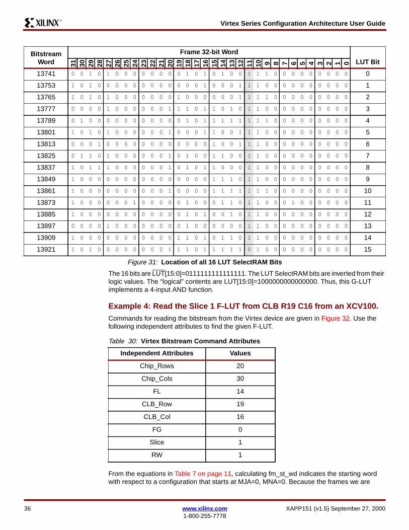
Virtex Series Configuration Architecture User GuideR13
The 16 bits are LUT[150]=0111111111111111 The LUT SelectRAM bits are inverted from theirlogic values The ldquologicalrdquo contents are LUT[150]=1000000000000000 Thus this G-LUTimplements a 4-input AND function
Example 4 Read the Slice 1 F-LUT from CLB R19 C16 from an XCV100Commands for reading the bitstream from the Virtex device are given in Figure 32 Use thefollowing independent attributes to find the given F-LUT
From the equations in Table 7 on page 11 calculating fm_st_wd indicates the starting wordwith respect to a configuration that starts at MJA=0 MNA=0 Because the frames we are
BitstreamWord
Frame 32-bit Word
LUT Bit31 30 29 28 27 26 25 24 23 22 21 20 19 18 17 16 15 14 13 12 11 10 9 8 7 6 5 4 3 2 1 0
13741 0 0 1 0 1 0 0 0 0 0 0 0 0 1 0 1 0 1 0 0 1 1 1 0 0 0 0 0 0 0 0 0 0
13753 1 0 1 0 0 0 0 0 0 0 0 0 0 0 0 1 0 0 0 1 1 1 0 0 0 0 0 0 0 0 0 0 1
13765 1 0 1 0 1 0 0 0 0 0 0 0 1 0 0 0 0 0 0 1 1 1 1 0 0 0 0 0 0 0 0 0 2
13777 0 0 0 0 1 0 0 0 0 0 0 1 1 1 0 1 1 0 1 0 1 1 0 0 0 0 0 0 0 0 0 0 3
13789 0 1 0 0 0 0 0 0 0 0 0 0 0 1 0 1 1 1 1 1 1 1 1 0 0 0 0 0 0 0 0 0 4
13801 1 0 1 0 1 0 0 0 0 0 0 1 0 0 0 1 1 0 0 1 1 1 0 0 0 0 0 0 0 0 0 0 5
13813 0 0 0 1 0 0 0 0 0 0 0 0 0 0 0 0 1 0 0 1 1 1 0 0 0 0 0 0 0 0 0 0 6
13825 0 1 1 0 1 0 0 0 0 0 0 1 0 1 0 0 1 1 0 0 1 1 0 0 0 0 0 0 0 0 0 0 7
13837 1 0 1 1 1 0 0 0 0 0 0 1 0 1 0 1 1 0 0 0 1 1 0 0 0 0 0 0 0 0 0 0 8
13849 1 0 0 0 0 0 0 0 0 0 0 0 0 0 0 0 1 1 1 0 1 1 0 0 0 0 0 0 0 0 0 0 9
13861 1 0 0 0 0 0 0 0 0 0 0 1 0 0 0 0 1 1 1 1 1 1 1 0 0 0 0 0 0 0 0 0 10
13873 1 0 0 0 0 0 0 1 0 0 0 0 0 1 0 0 0 1 1 0 1 1 0 0 0 1 0 0 0 0 0 0 11
13885 1 0 0 0 0 0 0 0 0 0 0 0 0 1 0 1 0 0 1 0 1 1 0 0 0 0 0 0 0 0 0 0 12
13897 0 0 0 0 1 0 0 0 0 0 0 0 0 1 0 0 0 0 0 0 1 1 0 0 0 0 0 0 0 0 0 0 13
13909 1 0 0 0 0 0 0 0 0 0 0 0 1 1 0 1 0 1 1 0 1 1 0 0 0 0 0 0 0 0 0 0 14
13921 1 0 1 0 0 0 0 0 0 0 0 1 1 1 0 1 1 1 1 1 0 1 0 0 0 0 0 0 0 0 0 0 15
Figure 31 Location of all 16 LUT SelectRAM Bits
Table 30 Virtex Bitstream Command Attributes
Independent Attributes Values
Chip_Rows 20
Chip_Cols 30
FL 14
CLB_Row 19
CLB_Col 16
FG 0
Slice 1
RW 1
36 wwwxilinxcom XAPP151 (v15) September 27 20001-800-255-7778
Virtex Series Configuration Architecture User GuideR13
interested in start at MJA=1 MNA=0 which is fm_st_wd = 126 so the first 126 words are notneeded (0ndash125) Therefore to find the given Slice 1 F-LUT see Table 31
Sixteen frames need to be read one for each bit in the LUT SelectRAM The bits in LUTSelectRAMs in Slice 1 occur in the opposite order that they do for Slice 0 LUT SelectRAMs
Frames are read sequentially with ascending addresses If read in LUT bit order LUT[0]LUT[1] hellip LUT[15] These are stored in descending addresses which require 16 separateread operations each reading one data frame and one pad frame However if read inascending address order LUT[15] LUT[14] hellip LUT[0] all 16 data frames are read with asingle read operation This requires only one pad frame for all 16 frames Thus it takes lesstime to read ascending frames starting at MJA=1 MNA=0 and finishing with frame MJA=1MNA=15 The frames in the XCV100 contain 14 32-bit words and a single pad wordCommands for reading only the F-LUT data are given in Figure 32
Table 31 Variables Equations and Values for Slice 1 F-LUT
Variables Equations Values
MJA 16 gt 302 rArr 2times16 ndash 30 ndash1 1
MNA lut_bit + 32 ndash Slice times (2 times lut_bit +17)= [015] + 32 ndash (2 times [015] + 17)= 15 ndash [015]
0 151 142 133 12
4 115 106 97 8
8 79 6
10 511 4
12 313 214 115 0
fm_bit_idx 3 + 18 times 19 ndash 0+ 32 377
fm_st_wd 14 times (8 + (1ndash 1) times 48 + [150]) +1 times 14= 14 times (8 + [150]) +14= 126 + 14 times [150]
= 336126
fm_wd floor(37732) 11
fm_wd_bit_idx 31 + 32 times 11 ndash 377 6
XAPP151 (v15) September 27 2000 wwwxilinxcom 371-800-255-7778
Virtex Series Configuration Architecture User GuideR13
The 377th bit of each frame is the bit in the F-LUT This LUT SelectRAM bit is in the framersquosword index 11 bit index 6
The configuration bits for the given frame in Figure 33 are as follows LUT Bit 15 is in MJA=1MNA=0 fm_wd=11 at bit 6
LUT bit 0 is in MJA=1 MNA=15 fm_wd=11 at bit 6
InstructionData
Hex 31 30 29 28 27 26 25 24 23 22 21 20 19 18 17 16 15 14 13 12 11 10 9 8 7 6 5 4 3 2 1 0
Sync Word AA99 5566 1 0 1 0 1 0 1 0 1 0 0 1 1 0 0 1 0 1 0 1 0 1 0 1 0 1 1 0 0 1 1 0
Write next (1) word to FAR 3000 2001 0 0 1 1 0 0 0 0 0 0 0 0 0 0 0 0 0 0 1 0 0 0 0 0 0 0 0 0 0 0 0 1
CLB MJA = 1 MNA = 0 0002 0000 0 0 0 0 0 0 0 0 0 0 0 0 0 0 1 0 0 0 0 0 0 0 0 0 0 0 0 0 0 0 0 0
Write next word to CMD 3000 8001 0 0 1 1 0 0 0 0 0 0 0 0 0 0 0 0 1 0 0 0 0 0 0 0 0 0 0 0 0 0 0 1
Register value for RCFG 0000 0004 0 0 0 0 0 0 0 0 0 0 0 0 0 0 0 0 0 0 0 0 0 0 0 0 0 0 0 0 0 1 0 0
Read from FDRO 2800 60EE 0 0 1 0 1 0 0 0 0 0 0 0 0 0 0 0 0 1 1 0 0 0 0 0 1 1 1 0 1 1 1 0
Flush pipe 0000 0000 0 0 0 0 0 0 0 0 0 0 0 0 0 0 0 0 0 0 0 0 0 0 0 0 0 0 0 0 0 0 0 0
(Read 238 words)
Figure 32 Commands to read Slice 1 F-LUT
Frame WordFrame 32-bit Word
31 30 29 28 27 26 25 24 23 22 21 20 19 18 17 16 15 14 13 12 11 10 9 8 7 6 5 4 3 2 1 0
0 0 0 0 0 0 0 0 0 0 0 0 0 0 0 0 0 0 0 0 0 0 0 0 0 0 0 0 0 0 0 0 0
1 1 1 0 0 0 0 0 0 0 0 0 0 0 1 0 1 1 1 1 1 1 1 0 0 0 0 0 0 0 0 0 0
2 1 1 1 1 1 1 1 1 0 0 0 0 0 0 0 0 0 0 1 1 1 1 1 1 1 1 0 0 0 0 0 0
3 0 0 0 0 1 1 1 1 1 1 1 1 0 0 0 0 0 0 0 0 0 0 1 1 1 1 1 1 1 1 0 0
4 0 0 0 0 0 0 0 0 1 1 1 1 1 1 1 1 0 0 0 0 0 0 0 0 0 0 1 1 1 1 1 1
5 1 1 0 0 0 0 0 0 0 0 0 0 1 1 1 1 1 1 1 1 0 0 0 0 0 0 0 0 0 0 1 1
6 1 1 1 1 1 1 0 0 0 0 0 0 0 0 0 0 1 1 1 1 1 1 1 1 0 0 0 0 0 0 0 0
7 0 0 1 1 1 1 1 1 1 1 0 0 0 0 0 0 0 0 0 0 1 1 1 1 1 1 1 1 0 0 0 0
8 0 0 0 0 0 0 1 1 1 1 1 1 1 1 0 0 0 0 0 0 0 0 0 0 1 1 1 1 1 1 1 1
9 0 0 0 0 0 0 0 0 0 0 1 1 1 1 1 1 1 1 0 0 0 0 0 0 0 0 0 0 1 1 1 1
10 1 1 1 1 0 0 0 0 0 0 0 0 0 0 1 1 1 1 1 1 1 1 0 0 0 0 0 0 0 0 0 0
11 1 1 1 1 1 1 1 1 0 0 0 0 0 0 0 0 0 0 1 1 1 1 1 1 1 0 0 0 0 0 0 0
12 0 0 0 0 1 1 1 1 1 1 1 1 0 0 0 0 0 0 0 0 0 0 1 1 1 1 1 1 0 0 0 0
13 0 0 0 0 0 0 0 0 0 1 1 1 0 0 0 0 0 0 0 0 0 0 1 1 1 1 1 1 0 0 0 0
Figure 33 Frame Containing F-LUT[15]
Bit streamWord
Frame 32-bit WordFmWd31 30 29 28 27 26 25 24 23 22 21 20 19 18 17 16 15 14 13 12 11 10 9 8 7 6 5 4 3 2 1 0
336 0 0 0 0 0 0 0 0 0 0 0 0 0 0 0 0 0 0 0 0 0 0 0 0 0 0 0 0 0 0 0 0 0337 0 1 0 0 1 0 0 0 0 0 0 1 0 1 0 0 1 1 0 0 1 1 0 0 0 0 0 0 0 0 0 0 1338 1 0 1 1 0 0 1 1 0 0 0 0 0 0 0 0 0 0 1 0 1 1 0 0 1 1 0 0 0 0 0 0 2339 0 0 0 0 1 0 1 1 0 0 1 1 0 0 0 0 0 0 0 0 0 0 1 0 1 1 0 0 1 1 0 0 3340 0 0 0 0 0 0 0 0 1 0 1 1 0 0 1 1 0 0 0 0 0 0 0 0 0 0 1 0 1 1 0 0 4341 1 1 0 0 0 0 0 0 0 0 0 0 1 0 1 1 0 0 1 1 0 0 0 0 0 0 0 0 0 0 1 0 5342 1 1 0 0 1 1 0 0 0 0 0 0 0 0 0 0 1 0 1 1 0 0 1 1 0 0 0 0 0 0 0 0 6343 0 0 1 0 1 1 0 0 1 1 0 0 0 0 0 0 0 0 0 0 1 0 1 1 0 0 1 1 0 0 0 0 7
Figure 34 Frame Containing F-LUT [0]
38 wwwxilinxcom XAPP151 (v15) September 27 20001-800-255-7778
Virtex Series Configuration Architecture User GuideR13
For the sake of brevity here are the sixteen 11th words in the order they appear in thebitstream
The bits are LUT[150]=0111111111111111 The LUT SelectRAM bits are inverted from thelogic sense The logical contents are LUT[150]=1000000000000000 Thus this F-LUTimplements a 4-input AND gate
Example 5 Read All Bits in Slice 0 G-LUTs from CLB C2 and XCV50Given the following attributes the necessary values to find the G-LUT data can be computed
344 0 0 0 0 0 0 1 0 1 1 0 0 1 1 0 0 0 0 0 0 0 0 0 0 1 0 1 1 0 0 1 1 8345 0 0 0 0 0 0 0 0 0 0 1 0 1 1 0 0 1 1 0 0 0 0 0 0 0 0 0 0 1 0 1 1 9346 0 0 1 1 0 0 0 0 0 0 0 0 0 0 1 0 1 1 0 0 1 1 0 0 0 0 0 0 0 0 0 0 10347 1 1 1 1 1 0 1 1 0 0 0 0 0 0 0 0 0 0 1 0 1 1 1 0 1 1 0 1 0 0 0 0 11348 0 0 0 0 1 1 1 0 1 0 1 1 0 0 0 0 0 0 0 0 0 0 1 1 1 1 0 1 0 0 0 0 12349 0 0 0 0 0 1 0 0 0 0 1 0 0 0 0 0 0 0 0 0 0 0 0 0 0 0 0 0 0 0 0 0 13
Bit streamWord
Frame 32-bit WordFmWd31 30 29 28 27 26 25 24 23 22 21 20 19 18 17 16 15 14 13 12 11 10 9 8 7 6 5 4 3 2 1 0
Figure 34 Frame Containing F-LUT [0]
BitstreamWord
Frame 32-bit WordLUT Bit31 30 29 28 27 26 25 24 23 22 21 20 19 18 17 16 15 14 13 12 11 10 9 8 7 6 5 4 3 2 1 0
137 1 1 1 1 1 1 1 1 0 0 0 0 0 0 0 0 0 0 1 1 1 1 1 1 1 0 0 0 0 0 0 0 15151 1 0 1 1 1 0 1 1 0 0 0 0 0 0 0 0 0 0 1 0 1 1 1 0 1 1 0 0 0 0 0 0 14165 1 0 1 1 0 0 1 1 0 0 0 0 0 0 0 0 0 0 1 0 1 1 1 0 1 1 0 0 0 0 0 0 13179 1 0 1 1 1 0 1 1 0 0 0 0 0 0 0 0 0 0 1 0 1 1 1 0 1 1 0 0 0 0 0 0 12193 1 1 1 1 1 0 1 1 0 0 0 0 0 0 0 0 0 0 1 1 1 1 1 0 1 1 0 0 0 0 0 0 11207 1 1 1 1 1 1 1 1 0 0 0 0 0 0 0 0 0 0 1 1 1 1 1 1 1 1 1 0 1 0 0 0 10221 1 1 1 1 1 0 1 1 0 0 0 0 0 0 0 0 0 0 1 1 1 1 1 0 1 1 0 0 0 0 0 0 9235 1 0 1 1 1 0 1 1 0 0 0 0 0 0 0 0 0 0 1 0 1 1 1 0 1 1 0 0 0 0 0 0 8249 1 0 1 1 0 0 1 1 0 0 0 0 0 0 0 0 0 0 1 0 1 1 0 0 1 1 0 0 0 0 0 0 7263 1 0 1 1 0 1 1 1 1 0 0 0 0 0 0 0 0 0 1 0 1 1 0 1 1 1 0 0 0 0 0 0 6277 1 1 1 1 0 0 1 1 0 0 0 0 0 0 0 0 0 0 1 1 1 1 0 0 1 1 0 0 0 0 0 0 5291 1 1 1 1 1 1 1 1 0 0 0 0 0 0 0 0 0 0 1 1 1 1 1 1 1 1 0 0 0 0 0 0 4305 1 1 1 1 1 0 1 1 0 0 0 0 0 0 0 0 0 0 1 1 1 1 1 0 1 1 0 0 0 0 0 0 3319 1 0 1 1 0 1 1 1 0 0 0 0 0 0 0 0 0 0 1 0 1 1 0 1 1 1 0 0 0 0 0 0 2333 1 0 1 1 0 0 1 1 0 0 0 0 0 0 0 0 0 0 1 0 1 1 0 0 1 1 0 0 0 0 0 0 1347 1 1 1 1 1 0 1 1 0 0 0 0 0 0 0 0 0 0 1 0 1 1 1 0 1 1 0 1 0 0 0 0 0
Figure 35 Sixteen Words Containing the F-LUT bit
Table 32 All Bits Slice 0 GndashLUTs from CLB C2 and XCV50
Independent Attributes Values
Chip_Rows 16
Chip_Cols 24
FL 12
CLB_Row 116
CLB_Col 2
XAPP151 (v15) September 27 2000 wwwxilinxcom 391-800-255-7778
Virtex Series Configuration Architecture User GuideR13
From the equations in Table 7 the dependent variables can be calculated
Note that fm_bit_idx fm_wd and fm_wd_bit_idx have 16 values one for each row on theXCV50 Figure 37 shows where the data lies in the first frame which contains G[0] for the entirecolumn The process is the same for the other 15 frames The commands for reading the LUTSelectRAM data are given in Figure 36
From the calculation for fm_st_wd Frame 0 would start at word 12588 reading the wholeconfiguration The instructions in Figure 36 start at that word so word 0 (ignoring the 12 wordsin the pad frame) is the same as word 12588 of the entire CLB configuration The 12 words inthe frame are shown in Figure 37
FG 1
Slice 0
lut_bit 015
RW 1
Table 32 All Bits Slice 0 GndashLUTs from CLB C2 and XCV50 (Continued)
Independent Attributes Values
Table 33 Dependent Variables Equations and Values
Variables Equations Values
MJA 2 le 242 rArr 24 ndash 2times 2 + 2 22
MNAlut_bit + 32 ndash Slice times (2 times lut_bit + 17)= lut_bit + 32 ndash 0 times (2 times lut_bit + 17)= [015] + 32
032 436 840 1244
133 537 941 1345
234 638 1042 1456
335 739 1143 1547
fm_bit_idx3 + 18 times CLB_Row ndash 1+ 32 = 34 + 18 times[116]
152 5124 9196 13268
270 6142 10214 14286
388 7160 11232 15304
4106 8178 12250 16322
fm_st_wd12 times (8 + (22 ndash1) times 48 + MNA) + 1 times 12= 12 times (1016 + MNA) + 12= 12204 + 12 times MNA
0 12588 4 12636 8 12684 12 12732
1 12600 5 12648 9 12696 13 12744
2 12612 6 12660 10 12708 14 12756
3 12624 7 12672 11 12720 15 12768
fm_wd floor (fm_bit_idx32)
11 53 96 138
22 64 106 148
32 75 117 159
43 85 127 1610
fm_wd_bit_idx 31 + 32 times fm_wd ndash fm_bit_idx
111 53 927 1319
225 617 109 141
37 7 31 1123 1515
421 813 125 1629
40 wwwxilinxcom XAPP151 (v15) September 27 20001-800-255-7778
Virtex Series Configuration Architecture User GuideR13
The LUT SelectRAM bits have been shaded for ease of identification It can be seen from thecalculation of fm_bit_idx that the LUT SelectRAM bits are in the order 116 For example fromthe above calculations for fm_wd and fm_wd_bit_idx G-LUT[0] in R1C2 is in fm_wd 1fm_wd_bit_idx 11 This bit is the shaded bit in word 1 at bit index 11 Similarly the G-LUT[0] forthe other 15 CLB rows are also shaded in this table
Example 6 Read Block SelectRAM index 387 of RAM R2 C0 from anXCV100ECommands for reading the bitstream from the Virtex device are given in Figure 38 Use thefollowing independent attributes to find the given F-LUT
InstructionData
Hex 31 30 29 28 27 26 25 24 23 22 21 20 19 18 17 16 15 14 13 12 11 10 9 8 7 6 5 4 3 2 1 0
Sync Word AA99 5566 1 0 1 0 1 0 1 0 1 0 0 1 1 0 0 1 0 1 0 1 0 1 0 1 0 1 1 0 0 1 1 0
Write next (1) word to FAR 3000 2001 0 0 1 1 0 0 0 0 0 0 0 0 0 0 0 0 0 0 1 0 0 0 0 0 0 0 0 0 0 0 0 1
CLB MJA=22 MNA=32 002C 4000 0 0 0 0 0 0 0 0 0 0 1 0 1 1 0 0 0 1 0 0 0 0 0 0 0 0 0 0 0 0 0 0
Write next word to CMD 3000 8001 0 0 1 1 0 0 0 0 0 0 0 0 0 0 0 0 1 0 0 0 0 0 0 0 0 0 0 0 0 0 0 1
Register value for RCFG 0000 0004 0 0 0 0 0 0 0 0 0 0 0 0 0 0 0 0 0 0 0 0 0 0 0 0 0 0 0 0 0 1 0 0
Read from FDRO 2800 60CC 0 0 1 0 1 0 0 0 0 0 0 0 0 0 0 0 0 1 1 0 0 0 0 0 1 1 0 0 1 1 0 0
Flush pipe 0000 0000 0 0 0 0 0 0 0 0 0 0 0 0 0 0 0 0 0 0 0 0 0 0 0 0 0 0 0 0 0 0 0 0
(Read 204 words)
Figure 36 Commands to read RC2S0 G-LUT
WordFrame 32-bit Word
CLB Row31 30 29 28 27 26 25 24 23 22 21 20 19 18 17 16 15 14 13 12 11 10 9 8 7 6 5 4 3 2 1 0
0 0 0 0 0 0 0 0 0 0 0 0 0 0 0 0 0 0 0 0 0 0 0 0 0 0 0 0 0 0 0 0 0
1 0 0 0 0 1 0 0 0 0 0 0 0 0 1 0 1 0 1 0 0 1 1 0 0 0 0 0 0 0 0 0 0 12 1 0 1 1 0 0 1 1 0 0 0 0 0 0 0 0 0 0 1 0 1 1 0 0 1 1 0 0 0 0 0 0 2 33 0 0 0 0 1 0 1 1 0 0 1 1 0 0 0 0 0 0 0 0 0 0 1 0 1 1 0 0 1 1 0 0 4 54 0 0 0 0 0 0 0 0 1 0 1 1 0 0 1 1 0 0 0 0 0 0 0 0 0 0 1 0 1 1 0 0 65 1 1 0 0 0 0 0 0 0 0 0 0 1 0 1 1 0 0 1 1 0 0 0 0 0 0 0 0 0 0 1 0 7 86 1 1 0 0 1 1 0 0 0 0 0 0 0 0 0 0 1 0 1 1 0 0 1 1 0 0 0 0 0 0 0 0 9 107 0 0 1 0 1 1 0 0 1 1 0 0 0 0 0 0 0 0 0 0 1 0 1 1 0 0 1 1 0 0 0 0 11 128 0 0 0 0 0 0 1 0 1 1 0 0 1 1 0 0 0 0 0 0 0 0 0 0 1 0 1 1 0 0 1 1 13 149 0 0 0 0 0 0 0 0 0 0 1 0 1 1 0 0 1 1 0 0 0 0 0 0 0 0 0 0 1 0 1 1 15
10 0 0 1 1 0 0 0 0 0 0 0 0 0 0 1 0 1 1 0 0 1 0 1 0 0 0 0 0 0 0 0 0 1611 0 1 0 1 0 0 0 0 0 0 0 0 0 0 0 0 0 0 0 0 0 0 0 0 0 0 0 0 0 0 0 0
Figure 37 Frame for RC2S0 G-LUTs Bit G[0]
Table 34 Virtex Bitstream Command Attributes
Independent Attributes Values
Chip_Rams 4
FL 14
RAM_Row 2
RAM_Col 0
ram_bit 387
RW 1
XAPP151 (v15) September 27 2000 wwwxilinxcom 411-800-255-7778
Virtex Series Configuration Architecture User GuideR13
Since we are attempting to read only one bit location only one frame is necessary to be readWe use the equations of Table 15 Table 16 and Table 17 to determine the dependentvariables
Commands for reading this memory index are given in Figure 38
RAM bit 387 is at fm_wd=6 bit 4
Table 35 Variables Equations and Values for Slice 1 F-LUT
Variables Equations Values
MJA_virtex 0 lt42 rArr 2times(42 -1 -0) 2
MJA_adj 0 lt42 rArr 2 2
MJA MJA_virtex + MJA_adj 4
MNA floor(((38764)64)32)+ 2 x floor(((38764)32)16)+ 4 x floor(((38764)16)8) + 8 x floor(((38764)8)4)+ 16 x floor(((38764)4)2) + 32 x floor(((38764)2)1)
24
fm_bit_idx 3 + 18 times 19 ndash 0 + 32 219
fm_st_wd 14 x 24 + 1 x 14 350
fm_wd floor(21932) 6
fm_wd_bit_idx 31 + 32 times 6 ndash 219 4
InstructionData
Hex 31 30 29 28 27 26 25 24 23 22 21 20 19 18 17 16 15 14 13 12 11 10 9 8 7 6 5 4 3 2 1 0
Sync Word AA99 5566 1 0 1 0 1 0 1 0 1 0 0 1 1 0 0 1 0 1 0 1 0 1 0 1 0 1 1 0 0 1 1 0
Write next (1) word to FAR 3000 2001 0 0 1 1 0 0 0 0 0 0 0 0 0 0 0 0 0 0 1 0 0 0 0 0 0 0 0 0 0 0 0 1
CLB MJA = 4 MNA = 24 0208 3000 0 0 0 0 0 0 1 0 0 0 0 0 1 0 0 0 0 0 1 1 0 0 0 0 0 0 0 0 0 0 0 0
Write next word to CMD 3000 8001 0 0 1 1 0 0 0 0 0 0 0 0 0 0 0 0 1 0 0 0 0 0 0 0 0 0 0 0 0 0 0 1
Register value for RCFG 0000 0004 0 0 0 0 0 0 0 0 0 0 0 0 0 0 0 0 0 0 0 0 0 0 0 0 0 0 0 0 0 1 0 0
Read from FDRO 2800 601C 0 0 1 0 1 0 0 0 0 0 0 0 0 0 0 0 0 1 1 0 0 0 0 0 0 0 0 1 1 1 0 0
Flush pipe 0000 0000 0 0 0 0 0 0 0 0 0 0 0 0 0 0 0 0 0 0 0 0 0 0 0 0 0 0 0 0 0 0 0 0
(Read 28 words)
Figure 38 Commands to read Block SelectRAM index 387
42 wwwxilinxcom XAPP151 (v15) September 27 20001-800-255-7778
Virtex Series Configuration Architecture User GuideR13
Glossary Block SelectRAM Resource
One of several large fully-synchronous dual-port memories in the Virtex FPGAs Each ofthese memories contain 4096 bits The organization of each memory is configurable Theblock SelectRAM resource complements the smaller distributed LUT SelectRAMs
Boundary Scan Interface
One of the configuration interfaces on the Virtex device This is a bit-serial interface TheBoundary Scan interface is also known as the JTAG port Also see the SelectMAP interface
Capture Data
The flip-flop and pad data saved from the logic cells and IO blocks into the bitstream Use theCAPTURE_VIRTEX primitive in your HDL code to specify the trigger and clock for the captureoperation
Configurable Logic Block (CLB)
The functional elements for constructing logic circuits The Virtex CLB is made up of Sliceswhich contain Logic Cells
Configuration Bitstream
Configuration commands optionally with configuration data
Configuration Commands
Instructions for the Virtex device There are two classes of Configuration Command mdash Majorand Minor The Major Commands read and write data to configuration registers in the Virtexdevice The Minor commands instruct the Virtex configuration logic to perform specificfunctions See Command Register (CMD) on page 18
Configuration Data
Bits that directly define the state of programmable logic These are written to a Virtex device ina configuration bitstream and read as Readback Data from a Virtex device
Frame WordFrame 32-bit Word
31 30 29 28 27 26 25 24 23 22 21 20 19 18 17 16 15 14 13 12 11 10 9 8 7 6 5 4 3 2 1 0
0 0 0 0 0 0 0 0 0 0 0 0 0 0 0 0 0 0 0 0 0 0 0 0 0 0 0 0 0 0 0 0 0
1 1 1 0 0 0 0 0 0 0 0 0 0 0 1 0 1 1 1 1 1 1 1 0 0 0 0 0 0 0 0 0 0
2 1 1 1 1 1 1 1 1 0 0 0 0 0 0 0 0 0 0 1 1 1 1 1 1 1 1 0 0 0 0 0 0
3 0 0 0 0 1 1 1 1 1 1 1 1 0 0 0 0 0 0 0 0 0 0 1 1 1 1 1 1 1 1 0 0
4 0 0 0 0 0 0 0 0 1 1 1 1 1 1 1 1 0 0 0 0 0 0 0 0 0 0 1 1 1 1 1 1
5 1 1 0 0 0 0 0 0 0 0 0 0 1 1 1 1 1 1 1 1 0 0 0 0 0 0 0 0 0 0 1 1
6 1 1 1 1 1 1 0 0 0 0 0 0 0 0 0 0 1 1 1 1 1 1 1 1 0 0 0 0 0 0 0 0
7 0 0 1 1 1 1 1 1 1 1 0 0 0 0 0 0 0 0 0 0 1 1 1 1 1 1 1 1 0 0 0 0
8 0 0 0 0 0 0 1 1 1 1 1 1 1 1 0 0 0 0 0 0 0 0 0 0 1 1 1 1 1 1 1 1
9 0 0 0 0 0 0 0 0 0 0 1 1 1 1 1 1 1 1 0 0 0 0 0 0 0 0 0 0 1 1 1 1
10 1 1 1 1 0 0 0 0 0 0 0 0 0 0 1 1 1 1 1 1 1 1 0 0 0 0 0 0 0 0 0 0
11 1 1 1 1 1 1 1 1 0 0 0 0 0 0 0 0 0 0 1 1 1 1 1 1 1 0 0 0 0 0 0 0
12 0 0 0 0 1 1 1 1 1 1 1 1 0 0 0 0 0 0 0 0 0 0 1 1 1 1 1 1 0 0 0 0
13 0 0 0 0 0 0 0 0 0 1 1 1 0 0 0 0 0 0 0 0 0 0 1 1 1 1 1 1 0 0 0 0
Figure 39 Frame MNA=24
XAPP151 (v15) September 27 2000 wwwxilinxcom 431-800-255-7778
Virtex Series Configuration Architecture User GuideR13
Configuration Frame
The configuration bits in a Virtex device are organized in columns A column of CLBs with theIO blocks above and below the CLBs contain 48 frames of configuration bits The smallestnumber of bits that can be read or written through the configuration interfaces is one frame
Configuration Interface
A logical interface on the Virtex device through which configuration commands and data can beread and written A interface consists of one or more physical Device Pins
Configuration Readback
The operation of reading Configuration Data (also known as Readback Data) from a Virtexdevice
Device Pin
One of the electrical connections on the package containing the Virtex device
Frame
See Configuration Frame
Logic Cell (LC)
The basic building block of the Virtex CLB An LC includes a 4-input function generator carrylogic and a storage element
LUT SelectRAMs
Shallow RAM structures implemented in CLB Lookup Tables (LUTs) See also blockSelectRAM section
Pad
Pad bits are extra bits used to make the total number of bits in a frame an integral multiple of32 the number of bits in a configuration word A Pad Word is an extra word used at the end ofa Configuration Frame for pipelining A Pad Frame is an extra Configuration Frame used at thebeginning of a Configuration Readback and at the end of a Configuration Write for pipelining
Readback Data
Configuration data read from a Virtex device The data is organized as Configuration Frames
SelectMAP Interface
One of the configuration interfaces on the Virtex device This is a byte-serial interface The pinsin the SelectMAP interface may be used as user IO after configuration has been completed orremain configured as a configuration interface
Slice
A subdivision of the Virtex CLB There are two vertical slices in a Virtex CLB Each slicecontains two Logic Cells
Sync Word
A 32-bit word with a value that is used to synchronize the configuration logic
44 wwwxilinxcom XAPP151 (v15) September 27 20001-800-255-7778
Virtex Series Configuration Architecture User GuideR13
RevisionHistory
The following table shows the revision history for this document
Date Version Revision
061799 10 Initial Release
072799 11 Updated the following tables Table 5 equation for MNA Table 7equations for MJA amp fm_bit_idx
092099 12 Changes in page 5 Most formulae in Table 7 have been revisedDocumented pad capture value P Corrected bit locations inExamples
022200 13 Updated to include Virtex-E block SelectRAM Correctedfm_bit_idx (Right IOB) equations in Table 12 and fm_st_wddefinition Corrected CRC algorithm Various corrections inExamples Reformatted and edited document and figures
080300 14 Updated to include Virtex-EM devices in Table 3 and Table 24
092700 15 Added Partial Reconfiguration of CLB section and Figure 26
XAPP151 (v15) September 27 2000 wwwxilinxcom 451-800-255-7778
- Summary
- Introduction
-
- CLBs IOBs and Configurations
-
- Configuring Virtex Devices
- Reading Configuration Bits From a Virtex Device
-
- Configuration Columns
- Configuration Addressing
-
- Block Type Major Address Minor Address
-
- Virtex Major Addresses
- Virtex-EM Major Addresses
- Virtex-E Major Addresses
-
- Frames
-
- Frame Sizes
- Frame Organization
- Location of LUT SelectRAM Bits
-
- Configuration Data Operations
-
- Reading Configuration Data
- Writing Configuration Data
- Altering Configuration Data
-
- Definitions
- CLB LUT SelectRAM Dependent Variables
-
- Virtex-E CLB LUT SelectRAM Dependent Variables
- LUT SelectRAM Examples
-
- CLB Flip-Flop Dependent Variables
-
- Virtex-E CLB Flip-Flop Dependent Variables
-
- IOB Dependent Variables
-
- Virtex-E IOB Dependent Variables
-
- Block SelectRAM Dependent Variables
-
- Virtex-E Block SelectRAM Dependent Variables
-
- Configuration Logic Basics
-
- Configuration Data
- Configuration Flow
-
- For Initial Configuration
- Reading Configuration
- Writing Configuration
-
- Configuration Registers
-
- Command Register (CMD)
- Configuration Option Register (COR)
- Control Register (CTL)
- Cyclic Redundancy Check (CRC)
-
- CRC Algorithm
-
- Frame Address Register (FAR)
- Frame Data Input Register (FDRI)
- Frame Data Output Register (FDRO)
- Frame Length Register (FLR)
- Legacy Output Register (LOUT)
- Mask Register (MASK)
- Status Register (STAT)
-
- Configuration Interface
- Partial Reconfiguration of CLBs
- Examples
-
- Example 1 Read and Write Semaphores in an XCV100 at CLB R1 C1 Slice 0
- Example 2 Reading the Complete Configuration from an XCV50
- Example 3 Read the Slice 0 G-LUT from CLB R1 C1 from the Complete Configuration of an XCV50
- Example 4 Read the Slice 1 F-LUT from CLB R19 C16 from an XCV100
- Example 5 Read All Bits in Slice 0 G-LUTs from CLB C2 and XCV50
- Example 6 Read Block SelectRAM index 387 of RAM R2 C0 from an XCV100E
-
- Glossary
-
- Block SelectRAM Resource
- Boundary Scan Interface
- Capture Data
- Configurable Logic Block (CLB)
- Configuration Bitstream
- Configuration Commands
- Configuration Data
- Configuration Frame
- Configuration Interface
- Configuration Readback
- Device Pin
- Frame
- Logic Cell (LC)
- LUT SelectRAMs
- Pad
- Readback Data
- SelectMAP Interface
- Slice
- Sync Word
-
- Revision History
-
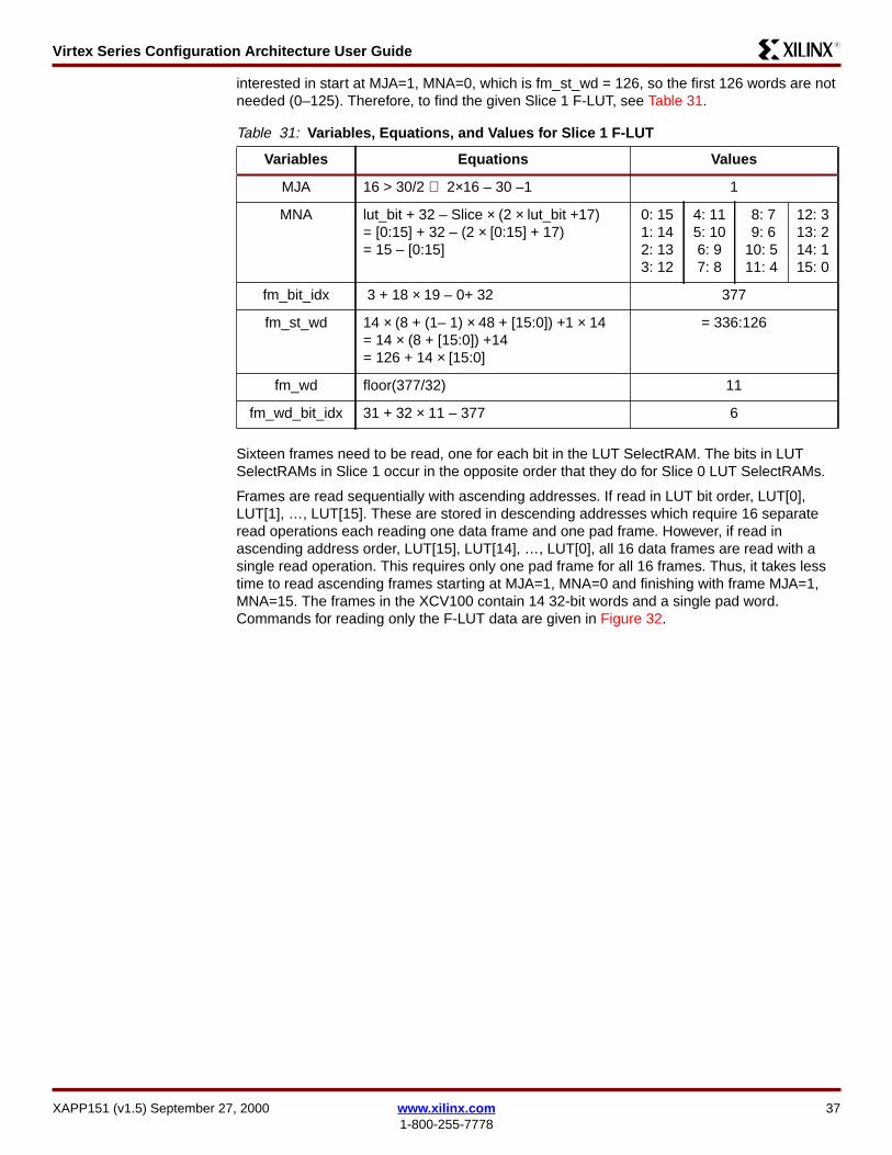
Virtex Series Configuration Architecture User GuideR13
The 377th bit of each frame is the bit in the F-LUT This LUT SelectRAM bit is in the framersquosword index 11 bit index 6
The configuration bits for the given frame in Figure 33 are as follows LUT Bit 15 is in MJA=1MNA=0 fm_wd=11 at bit 6
LUT bit 0 is in MJA=1 MNA=15 fm_wd=11 at bit 6
InstructionData
Hex 31 30 29 28 27 26 25 24 23 22 21 20 19 18 17 16 15 14 13 12 11 10 9 8 7 6 5 4 3 2 1 0
Sync Word AA99 5566 1 0 1 0 1 0 1 0 1 0 0 1 1 0 0 1 0 1 0 1 0 1 0 1 0 1 1 0 0 1 1 0
Write next (1) word to FAR 3000 2001 0 0 1 1 0 0 0 0 0 0 0 0 0 0 0 0 0 0 1 0 0 0 0 0 0 0 0 0 0 0 0 1
CLB MJA = 1 MNA = 0 0002 0000 0 0 0 0 0 0 0 0 0 0 0 0 0 0 1 0 0 0 0 0 0 0 0 0 0 0 0 0 0 0 0 0
Write next word to CMD 3000 8001 0 0 1 1 0 0 0 0 0 0 0 0 0 0 0 0 1 0 0 0 0 0 0 0 0 0 0 0 0 0 0 1
Register value for RCFG 0000 0004 0 0 0 0 0 0 0 0 0 0 0 0 0 0 0 0 0 0 0 0 0 0 0 0 0 0 0 0 0 1 0 0
Read from FDRO 2800 60EE 0 0 1 0 1 0 0 0 0 0 0 0 0 0 0 0 0 1 1 0 0 0 0 0 1 1 1 0 1 1 1 0
Flush pipe 0000 0000 0 0 0 0 0 0 0 0 0 0 0 0 0 0 0 0 0 0 0 0 0 0 0 0 0 0 0 0 0 0 0 0
(Read 238 words)
Figure 32 Commands to read Slice 1 F-LUT
Frame WordFrame 32-bit Word
31 30 29 28 27 26 25 24 23 22 21 20 19 18 17 16 15 14 13 12 11 10 9 8 7 6 5 4 3 2 1 0
0 0 0 0 0 0 0 0 0 0 0 0 0 0 0 0 0 0 0 0 0 0 0 0 0 0 0 0 0 0 0 0 0
1 1 1 0 0 0 0 0 0 0 0 0 0 0 1 0 1 1 1 1 1 1 1 0 0 0 0 0 0 0 0 0 0
2 1 1 1 1 1 1 1 1 0 0 0 0 0 0 0 0 0 0 1 1 1 1 1 1 1 1 0 0 0 0 0 0
3 0 0 0 0 1 1 1 1 1 1 1 1 0 0 0 0 0 0 0 0 0 0 1 1 1 1 1 1 1 1 0 0
4 0 0 0 0 0 0 0 0 1 1 1 1 1 1 1 1 0 0 0 0 0 0 0 0 0 0 1 1 1 1 1 1
5 1 1 0 0 0 0 0 0 0 0 0 0 1 1 1 1 1 1 1 1 0 0 0 0 0 0 0 0 0 0 1 1
6 1 1 1 1 1 1 0 0 0 0 0 0 0 0 0 0 1 1 1 1 1 1 1 1 0 0 0 0 0 0 0 0
7 0 0 1 1 1 1 1 1 1 1 0 0 0 0 0 0 0 0 0 0 1 1 1 1 1 1 1 1 0 0 0 0
8 0 0 0 0 0 0 1 1 1 1 1 1 1 1 0 0 0 0 0 0 0 0 0 0 1 1 1 1 1 1 1 1
9 0 0 0 0 0 0 0 0 0 0 1 1 1 1 1 1 1 1 0 0 0 0 0 0 0 0 0 0 1 1 1 1
10 1 1 1 1 0 0 0 0 0 0 0 0 0 0 1 1 1 1 1 1 1 1 0 0 0 0 0 0 0 0 0 0
11 1 1 1 1 1 1 1 1 0 0 0 0 0 0 0 0 0 0 1 1 1 1 1 1 1 0 0 0 0 0 0 0
12 0 0 0 0 1 1 1 1 1 1 1 1 0 0 0 0 0 0 0 0 0 0 1 1 1 1 1 1 0 0 0 0
13 0 0 0 0 0 0 0 0 0 1 1 1 0 0 0 0 0 0 0 0 0 0 1 1 1 1 1 1 0 0 0 0
Figure 33 Frame Containing F-LUT[15]
Bit streamWord
Frame 32-bit WordFmWd31 30 29 28 27 26 25 24 23 22 21 20 19 18 17 16 15 14 13 12 11 10 9 8 7 6 5 4 3 2 1 0
336 0 0 0 0 0 0 0 0 0 0 0 0 0 0 0 0 0 0 0 0 0 0 0 0 0 0 0 0 0 0 0 0 0337 0 1 0 0 1 0 0 0 0 0 0 1 0 1 0 0 1 1 0 0 1 1 0 0 0 0 0 0 0 0 0 0 1338 1 0 1 1 0 0 1 1 0 0 0 0 0 0 0 0 0 0 1 0 1 1 0 0 1 1 0 0 0 0 0 0 2339 0 0 0 0 1 0 1 1 0 0 1 1 0 0 0 0 0 0 0 0 0 0 1 0 1 1 0 0 1 1 0 0 3340 0 0 0 0 0 0 0 0 1 0 1 1 0 0 1 1 0 0 0 0 0 0 0 0 0 0 1 0 1 1 0 0 4341 1 1 0 0 0 0 0 0 0 0 0 0 1 0 1 1 0 0 1 1 0 0 0 0 0 0 0 0 0 0 1 0 5342 1 1 0 0 1 1 0 0 0 0 0 0 0 0 0 0 1 0 1 1 0 0 1 1 0 0 0 0 0 0 0 0 6343 0 0 1 0 1 1 0 0 1 1 0 0 0 0 0 0 0 0 0 0 1 0 1 1 0 0 1 1 0 0 0 0 7
Figure 34 Frame Containing F-LUT [0]
38 wwwxilinxcom XAPP151 (v15) September 27 20001-800-255-7778
Virtex Series Configuration Architecture User GuideR13
For the sake of brevity here are the sixteen 11th words in the order they appear in thebitstream
The bits are LUT[150]=0111111111111111 The LUT SelectRAM bits are inverted from thelogic sense The logical contents are LUT[150]=1000000000000000 Thus this F-LUTimplements a 4-input AND gate
Example 5 Read All Bits in Slice 0 G-LUTs from CLB C2 and XCV50Given the following attributes the necessary values to find the G-LUT data can be computed
344 0 0 0 0 0 0 1 0 1 1 0 0 1 1 0 0 0 0 0 0 0 0 0 0 1 0 1 1 0 0 1 1 8345 0 0 0 0 0 0 0 0 0 0 1 0 1 1 0 0 1 1 0 0 0 0 0 0 0 0 0 0 1 0 1 1 9346 0 0 1 1 0 0 0 0 0 0 0 0 0 0 1 0 1 1 0 0 1 1 0 0 0 0 0 0 0 0 0 0 10347 1 1 1 1 1 0 1 1 0 0 0 0 0 0 0 0 0 0 1 0 1 1 1 0 1 1 0 1 0 0 0 0 11348 0 0 0 0 1 1 1 0 1 0 1 1 0 0 0 0 0 0 0 0 0 0 1 1 1 1 0 1 0 0 0 0 12349 0 0 0 0 0 1 0 0 0 0 1 0 0 0 0 0 0 0 0 0 0 0 0 0 0 0 0 0 0 0 0 0 13
Bit streamWord
Frame 32-bit WordFmWd31 30 29 28 27 26 25 24 23 22 21 20 19 18 17 16 15 14 13 12 11 10 9 8 7 6 5 4 3 2 1 0
Figure 34 Frame Containing F-LUT [0]
BitstreamWord
Frame 32-bit WordLUT Bit31 30 29 28 27 26 25 24 23 22 21 20 19 18 17 16 15 14 13 12 11 10 9 8 7 6 5 4 3 2 1 0
137 1 1 1 1 1 1 1 1 0 0 0 0 0 0 0 0 0 0 1 1 1 1 1 1 1 0 0 0 0 0 0 0 15151 1 0 1 1 1 0 1 1 0 0 0 0 0 0 0 0 0 0 1 0 1 1 1 0 1 1 0 0 0 0 0 0 14165 1 0 1 1 0 0 1 1 0 0 0 0 0 0 0 0 0 0 1 0 1 1 1 0 1 1 0 0 0 0 0 0 13179 1 0 1 1 1 0 1 1 0 0 0 0 0 0 0 0 0 0 1 0 1 1 1 0 1 1 0 0 0 0 0 0 12193 1 1 1 1 1 0 1 1 0 0 0 0 0 0 0 0 0 0 1 1 1 1 1 0 1 1 0 0 0 0 0 0 11207 1 1 1 1 1 1 1 1 0 0 0 0 0 0 0 0 0 0 1 1 1 1 1 1 1 1 1 0 1 0 0 0 10221 1 1 1 1 1 0 1 1 0 0 0 0 0 0 0 0 0 0 1 1 1 1 1 0 1 1 0 0 0 0 0 0 9235 1 0 1 1 1 0 1 1 0 0 0 0 0 0 0 0 0 0 1 0 1 1 1 0 1 1 0 0 0 0 0 0 8249 1 0 1 1 0 0 1 1 0 0 0 0 0 0 0 0 0 0 1 0 1 1 0 0 1 1 0 0 0 0 0 0 7263 1 0 1 1 0 1 1 1 1 0 0 0 0 0 0 0 0 0 1 0 1 1 0 1 1 1 0 0 0 0 0 0 6277 1 1 1 1 0 0 1 1 0 0 0 0 0 0 0 0 0 0 1 1 1 1 0 0 1 1 0 0 0 0 0 0 5291 1 1 1 1 1 1 1 1 0 0 0 0 0 0 0 0 0 0 1 1 1 1 1 1 1 1 0 0 0 0 0 0 4305 1 1 1 1 1 0 1 1 0 0 0 0 0 0 0 0 0 0 1 1 1 1 1 0 1 1 0 0 0 0 0 0 3319 1 0 1 1 0 1 1 1 0 0 0 0 0 0 0 0 0 0 1 0 1 1 0 1 1 1 0 0 0 0 0 0 2333 1 0 1 1 0 0 1 1 0 0 0 0 0 0 0 0 0 0 1 0 1 1 0 0 1 1 0 0 0 0 0 0 1347 1 1 1 1 1 0 1 1 0 0 0 0 0 0 0 0 0 0 1 0 1 1 1 0 1 1 0 1 0 0 0 0 0
Figure 35 Sixteen Words Containing the F-LUT bit
Table 32 All Bits Slice 0 GndashLUTs from CLB C2 and XCV50
Independent Attributes Values
Chip_Rows 16
Chip_Cols 24
FL 12
CLB_Row 116
CLB_Col 2
XAPP151 (v15) September 27 2000 wwwxilinxcom 391-800-255-7778
Virtex Series Configuration Architecture User GuideR13
From the equations in Table 7 the dependent variables can be calculated
Note that fm_bit_idx fm_wd and fm_wd_bit_idx have 16 values one for each row on theXCV50 Figure 37 shows where the data lies in the first frame which contains G[0] for the entirecolumn The process is the same for the other 15 frames The commands for reading the LUTSelectRAM data are given in Figure 36
From the calculation for fm_st_wd Frame 0 would start at word 12588 reading the wholeconfiguration The instructions in Figure 36 start at that word so word 0 (ignoring the 12 wordsin the pad frame) is the same as word 12588 of the entire CLB configuration The 12 words inthe frame are shown in Figure 37
FG 1
Slice 0
lut_bit 015
RW 1
Table 32 All Bits Slice 0 GndashLUTs from CLB C2 and XCV50 (Continued)
Independent Attributes Values
Table 33 Dependent Variables Equations and Values
Variables Equations Values
MJA 2 le 242 rArr 24 ndash 2times 2 + 2 22
MNAlut_bit + 32 ndash Slice times (2 times lut_bit + 17)= lut_bit + 32 ndash 0 times (2 times lut_bit + 17)= [015] + 32
032 436 840 1244
133 537 941 1345
234 638 1042 1456
335 739 1143 1547
fm_bit_idx3 + 18 times CLB_Row ndash 1+ 32 = 34 + 18 times[116]
152 5124 9196 13268
270 6142 10214 14286
388 7160 11232 15304
4106 8178 12250 16322
fm_st_wd12 times (8 + (22 ndash1) times 48 + MNA) + 1 times 12= 12 times (1016 + MNA) + 12= 12204 + 12 times MNA
0 12588 4 12636 8 12684 12 12732
1 12600 5 12648 9 12696 13 12744
2 12612 6 12660 10 12708 14 12756
3 12624 7 12672 11 12720 15 12768
fm_wd floor (fm_bit_idx32)
11 53 96 138
22 64 106 148
32 75 117 159
43 85 127 1610
fm_wd_bit_idx 31 + 32 times fm_wd ndash fm_bit_idx
111 53 927 1319
225 617 109 141
37 7 31 1123 1515
421 813 125 1629
40 wwwxilinxcom XAPP151 (v15) September 27 20001-800-255-7778
Virtex Series Configuration Architecture User GuideR13
The LUT SelectRAM bits have been shaded for ease of identification It can be seen from thecalculation of fm_bit_idx that the LUT SelectRAM bits are in the order 116 For example fromthe above calculations for fm_wd and fm_wd_bit_idx G-LUT[0] in R1C2 is in fm_wd 1fm_wd_bit_idx 11 This bit is the shaded bit in word 1 at bit index 11 Similarly the G-LUT[0] forthe other 15 CLB rows are also shaded in this table
Example 6 Read Block SelectRAM index 387 of RAM R2 C0 from anXCV100ECommands for reading the bitstream from the Virtex device are given in Figure 38 Use thefollowing independent attributes to find the given F-LUT
InstructionData
Hex 31 30 29 28 27 26 25 24 23 22 21 20 19 18 17 16 15 14 13 12 11 10 9 8 7 6 5 4 3 2 1 0
Sync Word AA99 5566 1 0 1 0 1 0 1 0 1 0 0 1 1 0 0 1 0 1 0 1 0 1 0 1 0 1 1 0 0 1 1 0
Write next (1) word to FAR 3000 2001 0 0 1 1 0 0 0 0 0 0 0 0 0 0 0 0 0 0 1 0 0 0 0 0 0 0 0 0 0 0 0 1
CLB MJA=22 MNA=32 002C 4000 0 0 0 0 0 0 0 0 0 0 1 0 1 1 0 0 0 1 0 0 0 0 0 0 0 0 0 0 0 0 0 0
Write next word to CMD 3000 8001 0 0 1 1 0 0 0 0 0 0 0 0 0 0 0 0 1 0 0 0 0 0 0 0 0 0 0 0 0 0 0 1
Register value for RCFG 0000 0004 0 0 0 0 0 0 0 0 0 0 0 0 0 0 0 0 0 0 0 0 0 0 0 0 0 0 0 0 0 1 0 0
Read from FDRO 2800 60CC 0 0 1 0 1 0 0 0 0 0 0 0 0 0 0 0 0 1 1 0 0 0 0 0 1 1 0 0 1 1 0 0
Flush pipe 0000 0000 0 0 0 0 0 0 0 0 0 0 0 0 0 0 0 0 0 0 0 0 0 0 0 0 0 0 0 0 0 0 0 0
(Read 204 words)
Figure 36 Commands to read RC2S0 G-LUT
WordFrame 32-bit Word
CLB Row31 30 29 28 27 26 25 24 23 22 21 20 19 18 17 16 15 14 13 12 11 10 9 8 7 6 5 4 3 2 1 0
0 0 0 0 0 0 0 0 0 0 0 0 0 0 0 0 0 0 0 0 0 0 0 0 0 0 0 0 0 0 0 0 0
1 0 0 0 0 1 0 0 0 0 0 0 0 0 1 0 1 0 1 0 0 1 1 0 0 0 0 0 0 0 0 0 0 12 1 0 1 1 0 0 1 1 0 0 0 0 0 0 0 0 0 0 1 0 1 1 0 0 1 1 0 0 0 0 0 0 2 33 0 0 0 0 1 0 1 1 0 0 1 1 0 0 0 0 0 0 0 0 0 0 1 0 1 1 0 0 1 1 0 0 4 54 0 0 0 0 0 0 0 0 1 0 1 1 0 0 1 1 0 0 0 0 0 0 0 0 0 0 1 0 1 1 0 0 65 1 1 0 0 0 0 0 0 0 0 0 0 1 0 1 1 0 0 1 1 0 0 0 0 0 0 0 0 0 0 1 0 7 86 1 1 0 0 1 1 0 0 0 0 0 0 0 0 0 0 1 0 1 1 0 0 1 1 0 0 0 0 0 0 0 0 9 107 0 0 1 0 1 1 0 0 1 1 0 0 0 0 0 0 0 0 0 0 1 0 1 1 0 0 1 1 0 0 0 0 11 128 0 0 0 0 0 0 1 0 1 1 0 0 1 1 0 0 0 0 0 0 0 0 0 0 1 0 1 1 0 0 1 1 13 149 0 0 0 0 0 0 0 0 0 0 1 0 1 1 0 0 1 1 0 0 0 0 0 0 0 0 0 0 1 0 1 1 15
10 0 0 1 1 0 0 0 0 0 0 0 0 0 0 1 0 1 1 0 0 1 0 1 0 0 0 0 0 0 0 0 0 1611 0 1 0 1 0 0 0 0 0 0 0 0 0 0 0 0 0 0 0 0 0 0 0 0 0 0 0 0 0 0 0 0
Figure 37 Frame for RC2S0 G-LUTs Bit G[0]
Table 34 Virtex Bitstream Command Attributes
Independent Attributes Values
Chip_Rams 4
FL 14
RAM_Row 2
RAM_Col 0
ram_bit 387
RW 1
XAPP151 (v15) September 27 2000 wwwxilinxcom 411-800-255-7778
Virtex Series Configuration Architecture User GuideR13
Since we are attempting to read only one bit location only one frame is necessary to be readWe use the equations of Table 15 Table 16 and Table 17 to determine the dependentvariables
Commands for reading this memory index are given in Figure 38
RAM bit 387 is at fm_wd=6 bit 4
Table 35 Variables Equations and Values for Slice 1 F-LUT
Variables Equations Values
MJA_virtex 0 lt42 rArr 2times(42 -1 -0) 2
MJA_adj 0 lt42 rArr 2 2
MJA MJA_virtex + MJA_adj 4
MNA floor(((38764)64)32)+ 2 x floor(((38764)32)16)+ 4 x floor(((38764)16)8) + 8 x floor(((38764)8)4)+ 16 x floor(((38764)4)2) + 32 x floor(((38764)2)1)
24
fm_bit_idx 3 + 18 times 19 ndash 0 + 32 219
fm_st_wd 14 x 24 + 1 x 14 350
fm_wd floor(21932) 6
fm_wd_bit_idx 31 + 32 times 6 ndash 219 4
InstructionData
Hex 31 30 29 28 27 26 25 24 23 22 21 20 19 18 17 16 15 14 13 12 11 10 9 8 7 6 5 4 3 2 1 0
Sync Word AA99 5566 1 0 1 0 1 0 1 0 1 0 0 1 1 0 0 1 0 1 0 1 0 1 0 1 0 1 1 0 0 1 1 0
Write next (1) word to FAR 3000 2001 0 0 1 1 0 0 0 0 0 0 0 0 0 0 0 0 0 0 1 0 0 0 0 0 0 0 0 0 0 0 0 1
CLB MJA = 4 MNA = 24 0208 3000 0 0 0 0 0 0 1 0 0 0 0 0 1 0 0 0 0 0 1 1 0 0 0 0 0 0 0 0 0 0 0 0
Write next word to CMD 3000 8001 0 0 1 1 0 0 0 0 0 0 0 0 0 0 0 0 1 0 0 0 0 0 0 0 0 0 0 0 0 0 0 1
Register value for RCFG 0000 0004 0 0 0 0 0 0 0 0 0 0 0 0 0 0 0 0 0 0 0 0 0 0 0 0 0 0 0 0 0 1 0 0
Read from FDRO 2800 601C 0 0 1 0 1 0 0 0 0 0 0 0 0 0 0 0 0 1 1 0 0 0 0 0 0 0 0 1 1 1 0 0
Flush pipe 0000 0000 0 0 0 0 0 0 0 0 0 0 0 0 0 0 0 0 0 0 0 0 0 0 0 0 0 0 0 0 0 0 0 0
(Read 28 words)
Figure 38 Commands to read Block SelectRAM index 387
42 wwwxilinxcom XAPP151 (v15) September 27 20001-800-255-7778
Virtex Series Configuration Architecture User GuideR13
Glossary Block SelectRAM Resource
One of several large fully-synchronous dual-port memories in the Virtex FPGAs Each ofthese memories contain 4096 bits The organization of each memory is configurable Theblock SelectRAM resource complements the smaller distributed LUT SelectRAMs
Boundary Scan Interface
One of the configuration interfaces on the Virtex device This is a bit-serial interface TheBoundary Scan interface is also known as the JTAG port Also see the SelectMAP interface
Capture Data
The flip-flop and pad data saved from the logic cells and IO blocks into the bitstream Use theCAPTURE_VIRTEX primitive in your HDL code to specify the trigger and clock for the captureoperation
Configurable Logic Block (CLB)
The functional elements for constructing logic circuits The Virtex CLB is made up of Sliceswhich contain Logic Cells
Configuration Bitstream
Configuration commands optionally with configuration data
Configuration Commands
Instructions for the Virtex device There are two classes of Configuration Command mdash Majorand Minor The Major Commands read and write data to configuration registers in the Virtexdevice The Minor commands instruct the Virtex configuration logic to perform specificfunctions See Command Register (CMD) on page 18
Configuration Data
Bits that directly define the state of programmable logic These are written to a Virtex device ina configuration bitstream and read as Readback Data from a Virtex device
Frame WordFrame 32-bit Word
31 30 29 28 27 26 25 24 23 22 21 20 19 18 17 16 15 14 13 12 11 10 9 8 7 6 5 4 3 2 1 0
0 0 0 0 0 0 0 0 0 0 0 0 0 0 0 0 0 0 0 0 0 0 0 0 0 0 0 0 0 0 0 0 0
1 1 1 0 0 0 0 0 0 0 0 0 0 0 1 0 1 1 1 1 1 1 1 0 0 0 0 0 0 0 0 0 0
2 1 1 1 1 1 1 1 1 0 0 0 0 0 0 0 0 0 0 1 1 1 1 1 1 1 1 0 0 0 0 0 0
3 0 0 0 0 1 1 1 1 1 1 1 1 0 0 0 0 0 0 0 0 0 0 1 1 1 1 1 1 1 1 0 0
4 0 0 0 0 0 0 0 0 1 1 1 1 1 1 1 1 0 0 0 0 0 0 0 0 0 0 1 1 1 1 1 1
5 1 1 0 0 0 0 0 0 0 0 0 0 1 1 1 1 1 1 1 1 0 0 0 0 0 0 0 0 0 0 1 1
6 1 1 1 1 1 1 0 0 0 0 0 0 0 0 0 0 1 1 1 1 1 1 1 1 0 0 0 0 0 0 0 0
7 0 0 1 1 1 1 1 1 1 1 0 0 0 0 0 0 0 0 0 0 1 1 1 1 1 1 1 1 0 0 0 0
8 0 0 0 0 0 0 1 1 1 1 1 1 1 1 0 0 0 0 0 0 0 0 0 0 1 1 1 1 1 1 1 1
9 0 0 0 0 0 0 0 0 0 0 1 1 1 1 1 1 1 1 0 0 0 0 0 0 0 0 0 0 1 1 1 1
10 1 1 1 1 0 0 0 0 0 0 0 0 0 0 1 1 1 1 1 1 1 1 0 0 0 0 0 0 0 0 0 0
11 1 1 1 1 1 1 1 1 0 0 0 0 0 0 0 0 0 0 1 1 1 1 1 1 1 0 0 0 0 0 0 0
12 0 0 0 0 1 1 1 1 1 1 1 1 0 0 0 0 0 0 0 0 0 0 1 1 1 1 1 1 0 0 0 0
13 0 0 0 0 0 0 0 0 0 1 1 1 0 0 0 0 0 0 0 0 0 0 1 1 1 1 1 1 0 0 0 0
Figure 39 Frame MNA=24
XAPP151 (v15) September 27 2000 wwwxilinxcom 431-800-255-7778
Virtex Series Configuration Architecture User GuideR13
Configuration Frame
The configuration bits in a Virtex device are organized in columns A column of CLBs with theIO blocks above and below the CLBs contain 48 frames of configuration bits The smallestnumber of bits that can be read or written through the configuration interfaces is one frame
Configuration Interface
A logical interface on the Virtex device through which configuration commands and data can beread and written A interface consists of one or more physical Device Pins
Configuration Readback
The operation of reading Configuration Data (also known as Readback Data) from a Virtexdevice
Device Pin
One of the electrical connections on the package containing the Virtex device
Frame
See Configuration Frame
Logic Cell (LC)
The basic building block of the Virtex CLB An LC includes a 4-input function generator carrylogic and a storage element
LUT SelectRAMs
Shallow RAM structures implemented in CLB Lookup Tables (LUTs) See also blockSelectRAM section
Pad
Pad bits are extra bits used to make the total number of bits in a frame an integral multiple of32 the number of bits in a configuration word A Pad Word is an extra word used at the end ofa Configuration Frame for pipelining A Pad Frame is an extra Configuration Frame used at thebeginning of a Configuration Readback and at the end of a Configuration Write for pipelining
Readback Data
Configuration data read from a Virtex device The data is organized as Configuration Frames
SelectMAP Interface
One of the configuration interfaces on the Virtex device This is a byte-serial interface The pinsin the SelectMAP interface may be used as user IO after configuration has been completed orremain configured as a configuration interface
Slice
A subdivision of the Virtex CLB There are two vertical slices in a Virtex CLB Each slicecontains two Logic Cells
Sync Word
A 32-bit word with a value that is used to synchronize the configuration logic
44 wwwxilinxcom XAPP151 (v15) September 27 20001-800-255-7778
Virtex Series Configuration Architecture User GuideR13
RevisionHistory
The following table shows the revision history for this document
Date Version Revision
061799 10 Initial Release
072799 11 Updated the following tables Table 5 equation for MNA Table 7equations for MJA amp fm_bit_idx
092099 12 Changes in page 5 Most formulae in Table 7 have been revisedDocumented pad capture value P Corrected bit locations inExamples
022200 13 Updated to include Virtex-E block SelectRAM Correctedfm_bit_idx (Right IOB) equations in Table 12 and fm_st_wddefinition Corrected CRC algorithm Various corrections inExamples Reformatted and edited document and figures
080300 14 Updated to include Virtex-EM devices in Table 3 and Table 24
092700 15 Added Partial Reconfiguration of CLB section and Figure 26
XAPP151 (v15) September 27 2000 wwwxilinxcom 451-800-255-7778
- Summary
- Introduction
-
- CLBs IOBs and Configurations
-
- Configuring Virtex Devices
- Reading Configuration Bits From a Virtex Device
-
- Configuration Columns
- Configuration Addressing
-
- Block Type Major Address Minor Address
-
- Virtex Major Addresses
- Virtex-EM Major Addresses
- Virtex-E Major Addresses
-
- Frames
-
- Frame Sizes
- Frame Organization
- Location of LUT SelectRAM Bits
-
- Configuration Data Operations
-
- Reading Configuration Data
- Writing Configuration Data
- Altering Configuration Data
-
- Definitions
- CLB LUT SelectRAM Dependent Variables
-
- Virtex-E CLB LUT SelectRAM Dependent Variables
- LUT SelectRAM Examples
-
- CLB Flip-Flop Dependent Variables
-
- Virtex-E CLB Flip-Flop Dependent Variables
-
- IOB Dependent Variables
-
- Virtex-E IOB Dependent Variables
-
- Block SelectRAM Dependent Variables
-
- Virtex-E Block SelectRAM Dependent Variables
-
- Configuration Logic Basics
-
- Configuration Data
- Configuration Flow
-
- For Initial Configuration
- Reading Configuration
- Writing Configuration
-
- Configuration Registers
-
- Command Register (CMD)
- Configuration Option Register (COR)
- Control Register (CTL)
- Cyclic Redundancy Check (CRC)
-
- CRC Algorithm
-
- Frame Address Register (FAR)
- Frame Data Input Register (FDRI)
- Frame Data Output Register (FDRO)
- Frame Length Register (FLR)
- Legacy Output Register (LOUT)
- Mask Register (MASK)
- Status Register (STAT)
-
- Configuration Interface
- Partial Reconfiguration of CLBs
- Examples
-
- Example 1 Read and Write Semaphores in an XCV100 at CLB R1 C1 Slice 0
- Example 2 Reading the Complete Configuration from an XCV50
- Example 3 Read the Slice 0 G-LUT from CLB R1 C1 from the Complete Configuration of an XCV50
- Example 4 Read the Slice 1 F-LUT from CLB R19 C16 from an XCV100
- Example 5 Read All Bits in Slice 0 G-LUTs from CLB C2 and XCV50
- Example 6 Read Block SelectRAM index 387 of RAM R2 C0 from an XCV100E
-
- Glossary
-
- Block SelectRAM Resource
- Boundary Scan Interface
- Capture Data
- Configurable Logic Block (CLB)
- Configuration Bitstream
- Configuration Commands
- Configuration Data
- Configuration Frame
- Configuration Interface
- Configuration Readback
- Device Pin
- Frame
- Logic Cell (LC)
- LUT SelectRAMs
- Pad
- Readback Data
- SelectMAP Interface
- Slice
- Sync Word
-
- Revision History
-
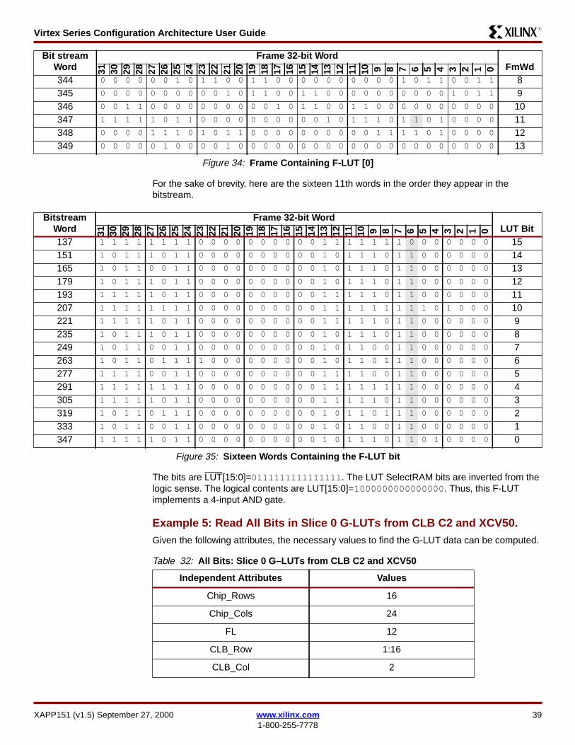
Virtex Series Configuration Architecture User GuideR13
The LUT SelectRAM bits have been shaded for ease of identification It can be seen from thecalculation of fm_bit_idx that the LUT SelectRAM bits are in the order 116 For example fromthe above calculations for fm_wd and fm_wd_bit_idx G-LUT[0] in R1C2 is in fm_wd 1fm_wd_bit_idx 11 This bit is the shaded bit in word 1 at bit index 11 Similarly the G-LUT[0] forthe other 15 CLB rows are also shaded in this table
Example 6 Read Block SelectRAM index 387 of RAM R2 C0 from anXCV100ECommands for reading the bitstream from the Virtex device are given in Figure 38 Use thefollowing independent attributes to find the given F-LUT
InstructionData
Hex 31 30 29 28 27 26 25 24 23 22 21 20 19 18 17 16 15 14 13 12 11 10 9 8 7 6 5 4 3 2 1 0
Sync Word AA99 5566 1 0 1 0 1 0 1 0 1 0 0 1 1 0 0 1 0 1 0 1 0 1 0 1 0 1 1 0 0 1 1 0
Write next (1) word to FAR 3000 2001 0 0 1 1 0 0 0 0 0 0 0 0 0 0 0 0 0 0 1 0 0 0 0 0 0 0 0 0 0 0 0 1
CLB MJA=22 MNA=32 002C 4000 0 0 0 0 0 0 0 0 0 0 1 0 1 1 0 0 0 1 0 0 0 0 0 0 0 0 0 0 0 0 0 0
Write next word to CMD 3000 8001 0 0 1 1 0 0 0 0 0 0 0 0 0 0 0 0 1 0 0 0 0 0 0 0 0 0 0 0 0 0 0 1
Register value for RCFG 0000 0004 0 0 0 0 0 0 0 0 0 0 0 0 0 0 0 0 0 0 0 0 0 0 0 0 0 0 0 0 0 1 0 0
Read from FDRO 2800 60CC 0 0 1 0 1 0 0 0 0 0 0 0 0 0 0 0 0 1 1 0 0 0 0 0 1 1 0 0 1 1 0 0
Flush pipe 0000 0000 0 0 0 0 0 0 0 0 0 0 0 0 0 0 0 0 0 0 0 0 0 0 0 0 0 0 0 0 0 0 0 0
(Read 204 words)
Figure 36 Commands to read RC2S0 G-LUT
WordFrame 32-bit Word
CLB Row31 30 29 28 27 26 25 24 23 22 21 20 19 18 17 16 15 14 13 12 11 10 9 8 7 6 5 4 3 2 1 0
0 0 0 0 0 0 0 0 0 0 0 0 0 0 0 0 0 0 0 0 0 0 0 0 0 0 0 0 0 0 0 0 0
1 0 0 0 0 1 0 0 0 0 0 0 0 0 1 0 1 0 1 0 0 1 1 0 0 0 0 0 0 0 0 0 0 12 1 0 1 1 0 0 1 1 0 0 0 0 0 0 0 0 0 0 1 0 1 1 0 0 1 1 0 0 0 0 0 0 2 33 0 0 0 0 1 0 1 1 0 0 1 1 0 0 0 0 0 0 0 0 0 0 1 0 1 1 0 0 1 1 0 0 4 54 0 0 0 0 0 0 0 0 1 0 1 1 0 0 1 1 0 0 0 0 0 0 0 0 0 0 1 0 1 1 0 0 65 1 1 0 0 0 0 0 0 0 0 0 0 1 0 1 1 0 0 1 1 0 0 0 0 0 0 0 0 0 0 1 0 7 86 1 1 0 0 1 1 0 0 0 0 0 0 0 0 0 0 1 0 1 1 0 0 1 1 0 0 0 0 0 0 0 0 9 107 0 0 1 0 1 1 0 0 1 1 0 0 0 0 0 0 0 0 0 0 1 0 1 1 0 0 1 1 0 0 0 0 11 128 0 0 0 0 0 0 1 0 1 1 0 0 1 1 0 0 0 0 0 0 0 0 0 0 1 0 1 1 0 0 1 1 13 149 0 0 0 0 0 0 0 0 0 0 1 0 1 1 0 0 1 1 0 0 0 0 0 0 0 0 0 0 1 0 1 1 15
10 0 0 1 1 0 0 0 0 0 0 0 0 0 0 1 0 1 1 0 0 1 0 1 0 0 0 0 0 0 0 0 0 1611 0 1 0 1 0 0 0 0 0 0 0 0 0 0 0 0 0 0 0 0 0 0 0 0 0 0 0 0 0 0 0 0
Figure 37 Frame for RC2S0 G-LUTs Bit G[0]
Table 34 Virtex Bitstream Command Attributes
Independent Attributes Values
Chip_Rams 4
FL 14
RAM_Row 2
RAM_Col 0
ram_bit 387
RW 1
XAPP151 (v15) September 27 2000 wwwxilinxcom 411-800-255-7778
Virtex Series Configuration Architecture User GuideR13
Since we are attempting to read only one bit location only one frame is necessary to be readWe use the equations of Table 15 Table 16 and Table 17 to determine the dependentvariables
Commands for reading this memory index are given in Figure 38
RAM bit 387 is at fm_wd=6 bit 4
Table 35 Variables Equations and Values for Slice 1 F-LUT
Variables Equations Values
MJA_virtex 0 lt42 rArr 2times(42 -1 -0) 2
MJA_adj 0 lt42 rArr 2 2
MJA MJA_virtex + MJA_adj 4
MNA floor(((38764)64)32)+ 2 x floor(((38764)32)16)+ 4 x floor(((38764)16)8) + 8 x floor(((38764)8)4)+ 16 x floor(((38764)4)2) + 32 x floor(((38764)2)1)
24
fm_bit_idx 3 + 18 times 19 ndash 0 + 32 219
fm_st_wd 14 x 24 + 1 x 14 350
fm_wd floor(21932) 6
fm_wd_bit_idx 31 + 32 times 6 ndash 219 4
InstructionData
Hex 31 30 29 28 27 26 25 24 23 22 21 20 19 18 17 16 15 14 13 12 11 10 9 8 7 6 5 4 3 2 1 0
Sync Word AA99 5566 1 0 1 0 1 0 1 0 1 0 0 1 1 0 0 1 0 1 0 1 0 1 0 1 0 1 1 0 0 1 1 0
Write next (1) word to FAR 3000 2001 0 0 1 1 0 0 0 0 0 0 0 0 0 0 0 0 0 0 1 0 0 0 0 0 0 0 0 0 0 0 0 1
CLB MJA = 4 MNA = 24 0208 3000 0 0 0 0 0 0 1 0 0 0 0 0 1 0 0 0 0 0 1 1 0 0 0 0 0 0 0 0 0 0 0 0
Write next word to CMD 3000 8001 0 0 1 1 0 0 0 0 0 0 0 0 0 0 0 0 1 0 0 0 0 0 0 0 0 0 0 0 0 0 0 1
Register value for RCFG 0000 0004 0 0 0 0 0 0 0 0 0 0 0 0 0 0 0 0 0 0 0 0 0 0 0 0 0 0 0 0 0 1 0 0
Read from FDRO 2800 601C 0 0 1 0 1 0 0 0 0 0 0 0 0 0 0 0 0 1 1 0 0 0 0 0 0 0 0 1 1 1 0 0
Flush pipe 0000 0000 0 0 0 0 0 0 0 0 0 0 0 0 0 0 0 0 0 0 0 0 0 0 0 0 0 0 0 0 0 0 0 0
(Read 28 words)
Figure 38 Commands to read Block SelectRAM index 387
42 wwwxilinxcom XAPP151 (v15) September 27 20001-800-255-7778
Virtex Series Configuration Architecture User GuideR13
Glossary Block SelectRAM Resource
One of several large fully-synchronous dual-port memories in the Virtex FPGAs Each ofthese memories contain 4096 bits The organization of each memory is configurable Theblock SelectRAM resource complements the smaller distributed LUT SelectRAMs
Boundary Scan Interface
One of the configuration interfaces on the Virtex device This is a bit-serial interface TheBoundary Scan interface is also known as the JTAG port Also see the SelectMAP interface
Capture Data
The flip-flop and pad data saved from the logic cells and IO blocks into the bitstream Use theCAPTURE_VIRTEX primitive in your HDL code to specify the trigger and clock for the captureoperation
Configurable Logic Block (CLB)
The functional elements for constructing logic circuits The Virtex CLB is made up of Sliceswhich contain Logic Cells
Configuration Bitstream
Configuration commands optionally with configuration data
Configuration Commands
Instructions for the Virtex device There are two classes of Configuration Command mdash Majorand Minor The Major Commands read and write data to configuration registers in the Virtexdevice The Minor commands instruct the Virtex configuration logic to perform specificfunctions See Command Register (CMD) on page 18
Configuration Data
Bits that directly define the state of programmable logic These are written to a Virtex device ina configuration bitstream and read as Readback Data from a Virtex device
Frame WordFrame 32-bit Word
31 30 29 28 27 26 25 24 23 22 21 20 19 18 17 16 15 14 13 12 11 10 9 8 7 6 5 4 3 2 1 0
0 0 0 0 0 0 0 0 0 0 0 0 0 0 0 0 0 0 0 0 0 0 0 0 0 0 0 0 0 0 0 0 0
1 1 1 0 0 0 0 0 0 0 0 0 0 0 1 0 1 1 1 1 1 1 1 0 0 0 0 0 0 0 0 0 0
2 1 1 1 1 1 1 1 1 0 0 0 0 0 0 0 0 0 0 1 1 1 1 1 1 1 1 0 0 0 0 0 0
3 0 0 0 0 1 1 1 1 1 1 1 1 0 0 0 0 0 0 0 0 0 0 1 1 1 1 1 1 1 1 0 0
4 0 0 0 0 0 0 0 0 1 1 1 1 1 1 1 1 0 0 0 0 0 0 0 0 0 0 1 1 1 1 1 1
5 1 1 0 0 0 0 0 0 0 0 0 0 1 1 1 1 1 1 1 1 0 0 0 0 0 0 0 0 0 0 1 1
6 1 1 1 1 1 1 0 0 0 0 0 0 0 0 0 0 1 1 1 1 1 1 1 1 0 0 0 0 0 0 0 0
7 0 0 1 1 1 1 1 1 1 1 0 0 0 0 0 0 0 0 0 0 1 1 1 1 1 1 1 1 0 0 0 0
8 0 0 0 0 0 0 1 1 1 1 1 1 1 1 0 0 0 0 0 0 0 0 0 0 1 1 1 1 1 1 1 1
9 0 0 0 0 0 0 0 0 0 0 1 1 1 1 1 1 1 1 0 0 0 0 0 0 0 0 0 0 1 1 1 1
10 1 1 1 1 0 0 0 0 0 0 0 0 0 0 1 1 1 1 1 1 1 1 0 0 0 0 0 0 0 0 0 0
11 1 1 1 1 1 1 1 1 0 0 0 0 0 0 0 0 0 0 1 1 1 1 1 1 1 0 0 0 0 0 0 0
12 0 0 0 0 1 1 1 1 1 1 1 1 0 0 0 0 0 0 0 0 0 0 1 1 1 1 1 1 0 0 0 0
13 0 0 0 0 0 0 0 0 0 1 1 1 0 0 0 0 0 0 0 0 0 0 1 1 1 1 1 1 0 0 0 0
Figure 39 Frame MNA=24
XAPP151 (v15) September 27 2000 wwwxilinxcom 431-800-255-7778
Virtex Series Configuration Architecture User GuideR13
Configuration Frame
The configuration bits in a Virtex device are organized in columns A column of CLBs with theIO blocks above and below the CLBs contain 48 frames of configuration bits The smallestnumber of bits that can be read or written through the configuration interfaces is one frame
Configuration Interface
A logical interface on the Virtex device through which configuration commands and data can beread and written A interface consists of one or more physical Device Pins
Configuration Readback
The operation of reading Configuration Data (also known as Readback Data) from a Virtexdevice
Device Pin
One of the electrical connections on the package containing the Virtex device
Frame
See Configuration Frame
Logic Cell (LC)
The basic building block of the Virtex CLB An LC includes a 4-input function generator carrylogic and a storage element
LUT SelectRAMs
Shallow RAM structures implemented in CLB Lookup Tables (LUTs) See also blockSelectRAM section
Pad
Pad bits are extra bits used to make the total number of bits in a frame an integral multiple of32 the number of bits in a configuration word A Pad Word is an extra word used at the end ofa Configuration Frame for pipelining A Pad Frame is an extra Configuration Frame used at thebeginning of a Configuration Readback and at the end of a Configuration Write for pipelining
Readback Data
Configuration data read from a Virtex device The data is organized as Configuration Frames
SelectMAP Interface
One of the configuration interfaces on the Virtex device This is a byte-serial interface The pinsin the SelectMAP interface may be used as user IO after configuration has been completed orremain configured as a configuration interface
Slice
A subdivision of the Virtex CLB There are two vertical slices in a Virtex CLB Each slicecontains two Logic Cells
Sync Word
A 32-bit word with a value that is used to synchronize the configuration logic
44 wwwxilinxcom XAPP151 (v15) September 27 20001-800-255-7778
Virtex Series Configuration Architecture User GuideR13
RevisionHistory
The following table shows the revision history for this document
Date Version Revision
061799 10 Initial Release
072799 11 Updated the following tables Table 5 equation for MNA Table 7equations for MJA amp fm_bit_idx
092099 12 Changes in page 5 Most formulae in Table 7 have been revisedDocumented pad capture value P Corrected bit locations inExamples
022200 13 Updated to include Virtex-E block SelectRAM Correctedfm_bit_idx (Right IOB) equations in Table 12 and fm_st_wddefinition Corrected CRC algorithm Various corrections inExamples Reformatted and edited document and figures
080300 14 Updated to include Virtex-EM devices in Table 3 and Table 24
092700 15 Added Partial Reconfiguration of CLB section and Figure 26
XAPP151 (v15) September 27 2000 wwwxilinxcom 451-800-255-7778
- Summary
- Introduction
-
- CLBs IOBs and Configurations
-
- Configuring Virtex Devices
- Reading Configuration Bits From a Virtex Device
-
- Configuration Columns
- Configuration Addressing
-
- Block Type Major Address Minor Address
-
- Virtex Major Addresses
- Virtex-EM Major Addresses
- Virtex-E Major Addresses
-
- Frames
-
- Frame Sizes
- Frame Organization
- Location of LUT SelectRAM Bits
-
- Configuration Data Operations
-
- Reading Configuration Data
- Writing Configuration Data
- Altering Configuration Data
-
- Definitions
- CLB LUT SelectRAM Dependent Variables
-
- Virtex-E CLB LUT SelectRAM Dependent Variables
- LUT SelectRAM Examples
-
- CLB Flip-Flop Dependent Variables
-
- Virtex-E CLB Flip-Flop Dependent Variables
-
- IOB Dependent Variables
-
- Virtex-E IOB Dependent Variables
-
- Block SelectRAM Dependent Variables
-
- Virtex-E Block SelectRAM Dependent Variables
-
- Configuration Logic Basics
-
- Configuration Data
- Configuration Flow
-
- For Initial Configuration
- Reading Configuration
- Writing Configuration
-
- Configuration Registers
-
- Command Register (CMD)
- Configuration Option Register (COR)
- Control Register (CTL)
- Cyclic Redundancy Check (CRC)
-
- CRC Algorithm
-
- Frame Address Register (FAR)
- Frame Data Input Register (FDRI)
- Frame Data Output Register (FDRO)
- Frame Length Register (FLR)
- Legacy Output Register (LOUT)
- Mask Register (MASK)
- Status Register (STAT)
-
- Configuration Interface
- Partial Reconfiguration of CLBs
- Examples
-
- Example 1 Read and Write Semaphores in an XCV100 at CLB R1 C1 Slice 0
- Example 2 Reading the Complete Configuration from an XCV50
- Example 3 Read the Slice 0 G-LUT from CLB R1 C1 from the Complete Configuration of an XCV50
- Example 4 Read the Slice 1 F-LUT from CLB R19 C16 from an XCV100
- Example 5 Read All Bits in Slice 0 G-LUTs from CLB C2 and XCV50
- Example 6 Read Block SelectRAM index 387 of RAM R2 C0 from an XCV100E
-
- Glossary
-
- Block SelectRAM Resource
- Boundary Scan Interface
- Capture Data
- Configurable Logic Block (CLB)
- Configuration Bitstream
- Configuration Commands
- Configuration Data
- Configuration Frame
- Configuration Interface
- Configuration Readback
- Device Pin
- Frame
- Logic Cell (LC)
- LUT SelectRAMs
- Pad
- Readback Data
- SelectMAP Interface
- Slice
- Sync Word
-
- Revision History
-
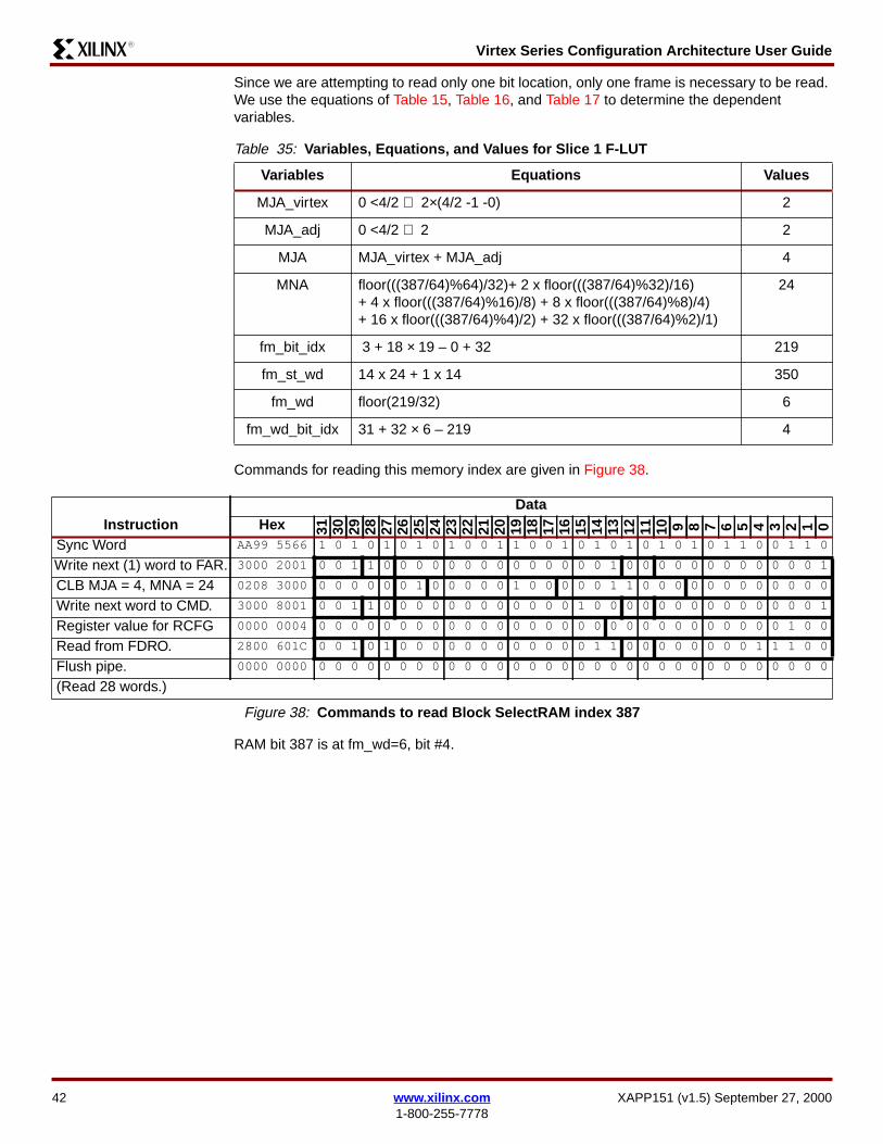
Virtex Series Configuration Architecture User GuideR13
Since we are attempting to read only one bit location only one frame is necessary to be readWe use the equations of Table 15 Table 16 and Table 17 to determine the dependentvariables
Commands for reading this memory index are given in Figure 38
RAM bit 387 is at fm_wd=6 bit 4
Table 35 Variables Equations and Values for Slice 1 F-LUT
Variables Equations Values
MJA_virtex 0 lt42 rArr 2times(42 -1 -0) 2
MJA_adj 0 lt42 rArr 2 2
MJA MJA_virtex + MJA_adj 4
MNA floor(((38764)64)32)+ 2 x floor(((38764)32)16)+ 4 x floor(((38764)16)8) + 8 x floor(((38764)8)4)+ 16 x floor(((38764)4)2) + 32 x floor(((38764)2)1)
24
fm_bit_idx 3 + 18 times 19 ndash 0 + 32 219
fm_st_wd 14 x 24 + 1 x 14 350
fm_wd floor(21932) 6
fm_wd_bit_idx 31 + 32 times 6 ndash 219 4
InstructionData
Hex 31 30 29 28 27 26 25 24 23 22 21 20 19 18 17 16 15 14 13 12 11 10 9 8 7 6 5 4 3 2 1 0
Sync Word AA99 5566 1 0 1 0 1 0 1 0 1 0 0 1 1 0 0 1 0 1 0 1 0 1 0 1 0 1 1 0 0 1 1 0
Write next (1) word to FAR 3000 2001 0 0 1 1 0 0 0 0 0 0 0 0 0 0 0 0 0 0 1 0 0 0 0 0 0 0 0 0 0 0 0 1
CLB MJA = 4 MNA = 24 0208 3000 0 0 0 0 0 0 1 0 0 0 0 0 1 0 0 0 0 0 1 1 0 0 0 0 0 0 0 0 0 0 0 0
Write next word to CMD 3000 8001 0 0 1 1 0 0 0 0 0 0 0 0 0 0 0 0 1 0 0 0 0 0 0 0 0 0 0 0 0 0 0 1
Register value for RCFG 0000 0004 0 0 0 0 0 0 0 0 0 0 0 0 0 0 0 0 0 0 0 0 0 0 0 0 0 0 0 0 0 1 0 0
Read from FDRO 2800 601C 0 0 1 0 1 0 0 0 0 0 0 0 0 0 0 0 0 1 1 0 0 0 0 0 0 0 0 1 1 1 0 0
Flush pipe 0000 0000 0 0 0 0 0 0 0 0 0 0 0 0 0 0 0 0 0 0 0 0 0 0 0 0 0 0 0 0 0 0 0 0
(Read 28 words)
Figure 38 Commands to read Block SelectRAM index 387
42 wwwxilinxcom XAPP151 (v15) September 27 20001-800-255-7778
Virtex Series Configuration Architecture User GuideR13
Glossary Block SelectRAM Resource
One of several large fully-synchronous dual-port memories in the Virtex FPGAs Each ofthese memories contain 4096 bits The organization of each memory is configurable Theblock SelectRAM resource complements the smaller distributed LUT SelectRAMs
Boundary Scan Interface
One of the configuration interfaces on the Virtex device This is a bit-serial interface TheBoundary Scan interface is also known as the JTAG port Also see the SelectMAP interface
Capture Data
The flip-flop and pad data saved from the logic cells and IO blocks into the bitstream Use theCAPTURE_VIRTEX primitive in your HDL code to specify the trigger and clock for the captureoperation
Configurable Logic Block (CLB)
The functional elements for constructing logic circuits The Virtex CLB is made up of Sliceswhich contain Logic Cells
Configuration Bitstream
Configuration commands optionally with configuration data
Configuration Commands
Instructions for the Virtex device There are two classes of Configuration Command mdash Majorand Minor The Major Commands read and write data to configuration registers in the Virtexdevice The Minor commands instruct the Virtex configuration logic to perform specificfunctions See Command Register (CMD) on page 18
Configuration Data
Bits that directly define the state of programmable logic These are written to a Virtex device ina configuration bitstream and read as Readback Data from a Virtex device
Frame WordFrame 32-bit Word
31 30 29 28 27 26 25 24 23 22 21 20 19 18 17 16 15 14 13 12 11 10 9 8 7 6 5 4 3 2 1 0
0 0 0 0 0 0 0 0 0 0 0 0 0 0 0 0 0 0 0 0 0 0 0 0 0 0 0 0 0 0 0 0 0
1 1 1 0 0 0 0 0 0 0 0 0 0 0 1 0 1 1 1 1 1 1 1 0 0 0 0 0 0 0 0 0 0
2 1 1 1 1 1 1 1 1 0 0 0 0 0 0 0 0 0 0 1 1 1 1 1 1 1 1 0 0 0 0 0 0
3 0 0 0 0 1 1 1 1 1 1 1 1 0 0 0 0 0 0 0 0 0 0 1 1 1 1 1 1 1 1 0 0
4 0 0 0 0 0 0 0 0 1 1 1 1 1 1 1 1 0 0 0 0 0 0 0 0 0 0 1 1 1 1 1 1
5 1 1 0 0 0 0 0 0 0 0 0 0 1 1 1 1 1 1 1 1 0 0 0 0 0 0 0 0 0 0 1 1
6 1 1 1 1 1 1 0 0 0 0 0 0 0 0 0 0 1 1 1 1 1 1 1 1 0 0 0 0 0 0 0 0
7 0 0 1 1 1 1 1 1 1 1 0 0 0 0 0 0 0 0 0 0 1 1 1 1 1 1 1 1 0 0 0 0
8 0 0 0 0 0 0 1 1 1 1 1 1 1 1 0 0 0 0 0 0 0 0 0 0 1 1 1 1 1 1 1 1
9 0 0 0 0 0 0 0 0 0 0 1 1 1 1 1 1 1 1 0 0 0 0 0 0 0 0 0 0 1 1 1 1
10 1 1 1 1 0 0 0 0 0 0 0 0 0 0 1 1 1 1 1 1 1 1 0 0 0 0 0 0 0 0 0 0
11 1 1 1 1 1 1 1 1 0 0 0 0 0 0 0 0 0 0 1 1 1 1 1 1 1 0 0 0 0 0 0 0
12 0 0 0 0 1 1 1 1 1 1 1 1 0 0 0 0 0 0 0 0 0 0 1 1 1 1 1 1 0 0 0 0
13 0 0 0 0 0 0 0 0 0 1 1 1 0 0 0 0 0 0 0 0 0 0 1 1 1 1 1 1 0 0 0 0
Figure 39 Frame MNA=24
XAPP151 (v15) September 27 2000 wwwxilinxcom 431-800-255-7778
Virtex Series Configuration Architecture User GuideR13
Configuration Frame
The configuration bits in a Virtex device are organized in columns A column of CLBs with theIO blocks above and below the CLBs contain 48 frames of configuration bits The smallestnumber of bits that can be read or written through the configuration interfaces is one frame
Configuration Interface
A logical interface on the Virtex device through which configuration commands and data can beread and written A interface consists of one or more physical Device Pins
Configuration Readback
The operation of reading Configuration Data (also known as Readback Data) from a Virtexdevice
Device Pin
One of the electrical connections on the package containing the Virtex device
Frame
See Configuration Frame
Logic Cell (LC)
The basic building block of the Virtex CLB An LC includes a 4-input function generator carrylogic and a storage element
LUT SelectRAMs
Shallow RAM structures implemented in CLB Lookup Tables (LUTs) See also blockSelectRAM section
Pad
Pad bits are extra bits used to make the total number of bits in a frame an integral multiple of32 the number of bits in a configuration word A Pad Word is an extra word used at the end ofa Configuration Frame for pipelining A Pad Frame is an extra Configuration Frame used at thebeginning of a Configuration Readback and at the end of a Configuration Write for pipelining
Readback Data
Configuration data read from a Virtex device The data is organized as Configuration Frames
SelectMAP Interface
One of the configuration interfaces on the Virtex device This is a byte-serial interface The pinsin the SelectMAP interface may be used as user IO after configuration has been completed orremain configured as a configuration interface
Slice
A subdivision of the Virtex CLB There are two vertical slices in a Virtex CLB Each slicecontains two Logic Cells
Sync Word
A 32-bit word with a value that is used to synchronize the configuration logic
44 wwwxilinxcom XAPP151 (v15) September 27 20001-800-255-7778
Virtex Series Configuration Architecture User GuideR13
RevisionHistory
The following table shows the revision history for this document
Date Version Revision
061799 10 Initial Release
072799 11 Updated the following tables Table 5 equation for MNA Table 7equations for MJA amp fm_bit_idx
092099 12 Changes in page 5 Most formulae in Table 7 have been revisedDocumented pad capture value P Corrected bit locations inExamples
022200 13 Updated to include Virtex-E block SelectRAM Correctedfm_bit_idx (Right IOB) equations in Table 12 and fm_st_wddefinition Corrected CRC algorithm Various corrections inExamples Reformatted and edited document and figures
080300 14 Updated to include Virtex-EM devices in Table 3 and Table 24
092700 15 Added Partial Reconfiguration of CLB section and Figure 26
XAPP151 (v15) September 27 2000 wwwxilinxcom 451-800-255-7778
- Summary
- Introduction
-
- CLBs IOBs and Configurations
-
- Configuring Virtex Devices
- Reading Configuration Bits From a Virtex Device
-
- Configuration Columns
- Configuration Addressing
-
- Block Type Major Address Minor Address
-
- Virtex Major Addresses
- Virtex-EM Major Addresses
- Virtex-E Major Addresses
-
- Frames
-
- Frame Sizes
- Frame Organization
- Location of LUT SelectRAM Bits
-
- Configuration Data Operations
-
- Reading Configuration Data
- Writing Configuration Data
- Altering Configuration Data
-
- Definitions
- CLB LUT SelectRAM Dependent Variables
-
- Virtex-E CLB LUT SelectRAM Dependent Variables
- LUT SelectRAM Examples
-
- CLB Flip-Flop Dependent Variables
-
- Virtex-E CLB Flip-Flop Dependent Variables
-
- IOB Dependent Variables
-
- Virtex-E IOB Dependent Variables
-
- Block SelectRAM Dependent Variables
-
- Virtex-E Block SelectRAM Dependent Variables
-
- Configuration Logic Basics
-
- Configuration Data
- Configuration Flow
-
- For Initial Configuration
- Reading Configuration
- Writing Configuration
-
- Configuration Registers
-
- Command Register (CMD)
- Configuration Option Register (COR)
- Control Register (CTL)
- Cyclic Redundancy Check (CRC)
-
- CRC Algorithm
-
- Frame Address Register (FAR)
- Frame Data Input Register (FDRI)
- Frame Data Output Register (FDRO)
- Frame Length Register (FLR)
- Legacy Output Register (LOUT)
- Mask Register (MASK)
- Status Register (STAT)
-
- Configuration Interface
- Partial Reconfiguration of CLBs
- Examples
-
- Example 1 Read and Write Semaphores in an XCV100 at CLB R1 C1 Slice 0
- Example 2 Reading the Complete Configuration from an XCV50
- Example 3 Read the Slice 0 G-LUT from CLB R1 C1 from the Complete Configuration of an XCV50
- Example 4 Read the Slice 1 F-LUT from CLB R19 C16 from an XCV100
- Example 5 Read All Bits in Slice 0 G-LUTs from CLB C2 and XCV50
- Example 6 Read Block SelectRAM index 387 of RAM R2 C0 from an XCV100E
-
- Glossary
-
- Block SelectRAM Resource
- Boundary Scan Interface
- Capture Data
- Configurable Logic Block (CLB)
- Configuration Bitstream
- Configuration Commands
- Configuration Data
- Configuration Frame
- Configuration Interface
- Configuration Readback
- Device Pin
- Frame
- Logic Cell (LC)
- LUT SelectRAMs
- Pad
- Readback Data
- SelectMAP Interface
- Slice
- Sync Word
-
- Revision History
-
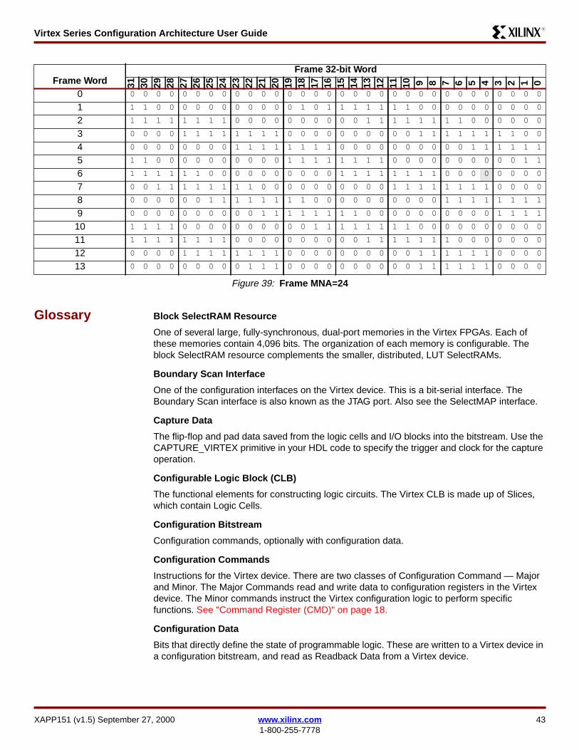
Virtex Series Configuration Architecture User GuideR13
Glossary Block SelectRAM Resource
One of several large fully-synchronous dual-port memories in the Virtex FPGAs Each ofthese memories contain 4096 bits The organization of each memory is configurable Theblock SelectRAM resource complements the smaller distributed LUT SelectRAMs
Boundary Scan Interface
One of the configuration interfaces on the Virtex device This is a bit-serial interface TheBoundary Scan interface is also known as the JTAG port Also see the SelectMAP interface
Capture Data
The flip-flop and pad data saved from the logic cells and IO blocks into the bitstream Use theCAPTURE_VIRTEX primitive in your HDL code to specify the trigger and clock for the captureoperation
Configurable Logic Block (CLB)
The functional elements for constructing logic circuits The Virtex CLB is made up of Sliceswhich contain Logic Cells
Configuration Bitstream
Configuration commands optionally with configuration data
Configuration Commands
Instructions for the Virtex device There are two classes of Configuration Command mdash Majorand Minor The Major Commands read and write data to configuration registers in the Virtexdevice The Minor commands instruct the Virtex configuration logic to perform specificfunctions See Command Register (CMD) on page 18
Configuration Data
Bits that directly define the state of programmable logic These are written to a Virtex device ina configuration bitstream and read as Readback Data from a Virtex device
Frame WordFrame 32-bit Word
31 30 29 28 27 26 25 24 23 22 21 20 19 18 17 16 15 14 13 12 11 10 9 8 7 6 5 4 3 2 1 0
0 0 0 0 0 0 0 0 0 0 0 0 0 0 0 0 0 0 0 0 0 0 0 0 0 0 0 0 0 0 0 0 0
1 1 1 0 0 0 0 0 0 0 0 0 0 0 1 0 1 1 1 1 1 1 1 0 0 0 0 0 0 0 0 0 0
2 1 1 1 1 1 1 1 1 0 0 0 0 0 0 0 0 0 0 1 1 1 1 1 1 1 1 0 0 0 0 0 0
3 0 0 0 0 1 1 1 1 1 1 1 1 0 0 0 0 0 0 0 0 0 0 1 1 1 1 1 1 1 1 0 0
4 0 0 0 0 0 0 0 0 1 1 1 1 1 1 1 1 0 0 0 0 0 0 0 0 0 0 1 1 1 1 1 1
5 1 1 0 0 0 0 0 0 0 0 0 0 1 1 1 1 1 1 1 1 0 0 0 0 0 0 0 0 0 0 1 1
6 1 1 1 1 1 1 0 0 0 0 0 0 0 0 0 0 1 1 1 1 1 1 1 1 0 0 0 0 0 0 0 0
7 0 0 1 1 1 1 1 1 1 1 0 0 0 0 0 0 0 0 0 0 1 1 1 1 1 1 1 1 0 0 0 0
8 0 0 0 0 0 0 1 1 1 1 1 1 1 1 0 0 0 0 0 0 0 0 0 0 1 1 1 1 1 1 1 1
9 0 0 0 0 0 0 0 0 0 0 1 1 1 1 1 1 1 1 0 0 0 0 0 0 0 0 0 0 1 1 1 1
10 1 1 1 1 0 0 0 0 0 0 0 0 0 0 1 1 1 1 1 1 1 1 0 0 0 0 0 0 0 0 0 0
11 1 1 1 1 1 1 1 1 0 0 0 0 0 0 0 0 0 0 1 1 1 1 1 1 1 0 0 0 0 0 0 0
12 0 0 0 0 1 1 1 1 1 1 1 1 0 0 0 0 0 0 0 0 0 0 1 1 1 1 1 1 0 0 0 0
13 0 0 0 0 0 0 0 0 0 1 1 1 0 0 0 0 0 0 0 0 0 0 1 1 1 1 1 1 0 0 0 0
Figure 39 Frame MNA=24
XAPP151 (v15) September 27 2000 wwwxilinxcom 431-800-255-7778
Virtex Series Configuration Architecture User GuideR13
Configuration Frame
The configuration bits in a Virtex device are organized in columns A column of CLBs with theIO blocks above and below the CLBs contain 48 frames of configuration bits The smallestnumber of bits that can be read or written through the configuration interfaces is one frame
Configuration Interface
A logical interface on the Virtex device through which configuration commands and data can beread and written A interface consists of one or more physical Device Pins
Configuration Readback
The operation of reading Configuration Data (also known as Readback Data) from a Virtexdevice
Device Pin
One of the electrical connections on the package containing the Virtex device
Frame
See Configuration Frame
Logic Cell (LC)
The basic building block of the Virtex CLB An LC includes a 4-input function generator carrylogic and a storage element
LUT SelectRAMs
Shallow RAM structures implemented in CLB Lookup Tables (LUTs) See also blockSelectRAM section
Pad
Pad bits are extra bits used to make the total number of bits in a frame an integral multiple of32 the number of bits in a configuration word A Pad Word is an extra word used at the end ofa Configuration Frame for pipelining A Pad Frame is an extra Configuration Frame used at thebeginning of a Configuration Readback and at the end of a Configuration Write for pipelining
Readback Data
Configuration data read from a Virtex device The data is organized as Configuration Frames
SelectMAP Interface
One of the configuration interfaces on the Virtex device This is a byte-serial interface The pinsin the SelectMAP interface may be used as user IO after configuration has been completed orremain configured as a configuration interface
Slice
A subdivision of the Virtex CLB There are two vertical slices in a Virtex CLB Each slicecontains two Logic Cells
Sync Word
A 32-bit word with a value that is used to synchronize the configuration logic
44 wwwxilinxcom XAPP151 (v15) September 27 20001-800-255-7778
Virtex Series Configuration Architecture User GuideR13
RevisionHistory
The following table shows the revision history for this document
Date Version Revision
061799 10 Initial Release
072799 11 Updated the following tables Table 5 equation for MNA Table 7equations for MJA amp fm_bit_idx
092099 12 Changes in page 5 Most formulae in Table 7 have been revisedDocumented pad capture value P Corrected bit locations inExamples
022200 13 Updated to include Virtex-E block SelectRAM Correctedfm_bit_idx (Right IOB) equations in Table 12 and fm_st_wddefinition Corrected CRC algorithm Various corrections inExamples Reformatted and edited document and figures
080300 14 Updated to include Virtex-EM devices in Table 3 and Table 24
092700 15 Added Partial Reconfiguration of CLB section and Figure 26
XAPP151 (v15) September 27 2000 wwwxilinxcom 451-800-255-7778
- Summary
- Introduction
-
- CLBs IOBs and Configurations
-
- Configuring Virtex Devices
- Reading Configuration Bits From a Virtex Device
-
- Configuration Columns
- Configuration Addressing
-
- Block Type Major Address Minor Address
-
- Virtex Major Addresses
- Virtex-EM Major Addresses
- Virtex-E Major Addresses
-
- Frames
-
- Frame Sizes
- Frame Organization
- Location of LUT SelectRAM Bits
-
- Configuration Data Operations
-
- Reading Configuration Data
- Writing Configuration Data
- Altering Configuration Data
-
- Definitions
- CLB LUT SelectRAM Dependent Variables
-
- Virtex-E CLB LUT SelectRAM Dependent Variables
- LUT SelectRAM Examples
-
- CLB Flip-Flop Dependent Variables
-
- Virtex-E CLB Flip-Flop Dependent Variables
-
- IOB Dependent Variables
-
- Virtex-E IOB Dependent Variables
-
- Block SelectRAM Dependent Variables
-
- Virtex-E Block SelectRAM Dependent Variables
-
- Configuration Logic Basics
-
- Configuration Data
- Configuration Flow
-
- For Initial Configuration
- Reading Configuration
- Writing Configuration
-
- Configuration Registers
-
- Command Register (CMD)
- Configuration Option Register (COR)
- Control Register (CTL)
- Cyclic Redundancy Check (CRC)
-
- CRC Algorithm
-
- Frame Address Register (FAR)
- Frame Data Input Register (FDRI)
- Frame Data Output Register (FDRO)
- Frame Length Register (FLR)
- Legacy Output Register (LOUT)
- Mask Register (MASK)
- Status Register (STAT)
-
- Configuration Interface
- Partial Reconfiguration of CLBs
- Examples
-
- Example 1 Read and Write Semaphores in an XCV100 at CLB R1 C1 Slice 0
- Example 2 Reading the Complete Configuration from an XCV50
- Example 3 Read the Slice 0 G-LUT from CLB R1 C1 from the Complete Configuration of an XCV50
- Example 4 Read the Slice 1 F-LUT from CLB R19 C16 from an XCV100
- Example 5 Read All Bits in Slice 0 G-LUTs from CLB C2 and XCV50
- Example 6 Read Block SelectRAM index 387 of RAM R2 C0 from an XCV100E
-
- Glossary
-
- Block SelectRAM Resource
- Boundary Scan Interface
- Capture Data
- Configurable Logic Block (CLB)
- Configuration Bitstream
- Configuration Commands
- Configuration Data
- Configuration Frame
- Configuration Interface
- Configuration Readback
- Device Pin
- Frame
- Logic Cell (LC)
- LUT SelectRAMs
- Pad
- Readback Data
- SelectMAP Interface
- Slice
- Sync Word
-
- Revision History
-
Virtex Series Configuration Architecture User GuideR13
Configuration Frame
The configuration bits in a Virtex device are organized in columns A column of CLBs with theIO blocks above and below the CLBs contain 48 frames of configuration bits The smallestnumber of bits that can be read or written through the configuration interfaces is one frame
Configuration Interface
A logical interface on the Virtex device through which configuration commands and data can beread and written A interface consists of one or more physical Device Pins
Configuration Readback
The operation of reading Configuration Data (also known as Readback Data) from a Virtexdevice
Device Pin
One of the electrical connections on the package containing the Virtex device
Frame
See Configuration Frame
Logic Cell (LC)
The basic building block of the Virtex CLB An LC includes a 4-input function generator carrylogic and a storage element
LUT SelectRAMs
Shallow RAM structures implemented in CLB Lookup Tables (LUTs) See also blockSelectRAM section
Pad
Pad bits are extra bits used to make the total number of bits in a frame an integral multiple of32 the number of bits in a configuration word A Pad Word is an extra word used at the end ofa Configuration Frame for pipelining A Pad Frame is an extra Configuration Frame used at thebeginning of a Configuration Readback and at the end of a Configuration Write for pipelining
Readback Data
Configuration data read from a Virtex device The data is organized as Configuration Frames
SelectMAP Interface
One of the configuration interfaces on the Virtex device This is a byte-serial interface The pinsin the SelectMAP interface may be used as user IO after configuration has been completed orremain configured as a configuration interface
Slice
A subdivision of the Virtex CLB There are two vertical slices in a Virtex CLB Each slicecontains two Logic Cells
Sync Word
A 32-bit word with a value that is used to synchronize the configuration logic
44 wwwxilinxcom XAPP151 (v15) September 27 20001-800-255-7778
Virtex Series Configuration Architecture User GuideR13
RevisionHistory
The following table shows the revision history for this document
Date Version Revision
061799 10 Initial Release
072799 11 Updated the following tables Table 5 equation for MNA Table 7equations for MJA amp fm_bit_idx
092099 12 Changes in page 5 Most formulae in Table 7 have been revisedDocumented pad capture value P Corrected bit locations inExamples
022200 13 Updated to include Virtex-E block SelectRAM Correctedfm_bit_idx (Right IOB) equations in Table 12 and fm_st_wddefinition Corrected CRC algorithm Various corrections inExamples Reformatted and edited document and figures
080300 14 Updated to include Virtex-EM devices in Table 3 and Table 24
092700 15 Added Partial Reconfiguration of CLB section and Figure 26
XAPP151 (v15) September 27 2000 wwwxilinxcom 451-800-255-7778
- Summary
- Introduction
-
- CLBs IOBs and Configurations
-
- Configuring Virtex Devices
- Reading Configuration Bits From a Virtex Device
-
- Configuration Columns
- Configuration Addressing
-
- Block Type Major Address Minor Address
-
- Virtex Major Addresses
- Virtex-EM Major Addresses
- Virtex-E Major Addresses
-
- Frames
-
- Frame Sizes
- Frame Organization
- Location of LUT SelectRAM Bits
-
- Configuration Data Operations
-
- Reading Configuration Data
- Writing Configuration Data
- Altering Configuration Data
-
- Definitions
- CLB LUT SelectRAM Dependent Variables
-
- Virtex-E CLB LUT SelectRAM Dependent Variables
- LUT SelectRAM Examples
-
- CLB Flip-Flop Dependent Variables
-
- Virtex-E CLB Flip-Flop Dependent Variables
-
- IOB Dependent Variables
-
- Virtex-E IOB Dependent Variables
-
- Block SelectRAM Dependent Variables
-
- Virtex-E Block SelectRAM Dependent Variables
-
- Configuration Logic Basics
-
- Configuration Data
- Configuration Flow
-
- For Initial Configuration
- Reading Configuration
- Writing Configuration
-
- Configuration Registers
-
- Command Register (CMD)
- Configuration Option Register (COR)
- Control Register (CTL)
- Cyclic Redundancy Check (CRC)
-
- CRC Algorithm
-
- Frame Address Register (FAR)
- Frame Data Input Register (FDRI)
- Frame Data Output Register (FDRO)
- Frame Length Register (FLR)
- Legacy Output Register (LOUT)
- Mask Register (MASK)
- Status Register (STAT)
-
- Configuration Interface
- Partial Reconfiguration of CLBs
- Examples
-
- Example 1 Read and Write Semaphores in an XCV100 at CLB R1 C1 Slice 0
- Example 2 Reading the Complete Configuration from an XCV50
- Example 3 Read the Slice 0 G-LUT from CLB R1 C1 from the Complete Configuration of an XCV50
- Example 4 Read the Slice 1 F-LUT from CLB R19 C16 from an XCV100
- Example 5 Read All Bits in Slice 0 G-LUTs from CLB C2 and XCV50
- Example 6 Read Block SelectRAM index 387 of RAM R2 C0 from an XCV100E
-
- Glossary
-
- Block SelectRAM Resource
- Boundary Scan Interface
- Capture Data
- Configurable Logic Block (CLB)
- Configuration Bitstream
- Configuration Commands
- Configuration Data
- Configuration Frame
- Configuration Interface
- Configuration Readback
- Device Pin
- Frame
- Logic Cell (LC)
- LUT SelectRAMs
- Pad
- Readback Data
- SelectMAP Interface
- Slice
- Sync Word
-
- Revision History
-