Viasystems Surface Finishes - Surface-mount technology
17
Solutions without Boundaries PCB Surface Finishes 1 PCB Surface Finishes Todd Henninger, C.I.D. Sr. Field Applications Engineer Midwest Region
Transcript of Viasystems Surface Finishes - Surface-mount technology
Solutions without Boundaries
PCB Surface Finishes
1
PCB Surface Finishes
Todd Henninger, C.I.D.
Sr. Field Applications Engineer
Midwest Region
� Notification of Proprietary Information: This document contains
proprietary information of Viasystems and its receipt or possession
Notice
2
does not convey any rights to reproduce or disclose its contents, or to
manufacture, use, or sell anything it may describe. Reproduction,
dissemination, disclosure, or use, in whole or in part, without specific
written authorization of Viasystems is strictly forbidden. All data
contained within this document are subject to this restriction.
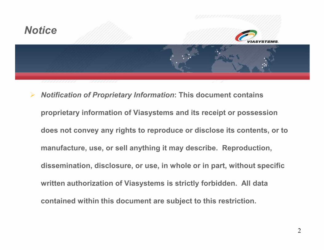
• All about the connectivity between the PCB and component devices.
• Primary function is to either temporarily protect the copper area from
oxidation prior to assembly or to form the foundation of the connection
to the electronic device.
Surface Finish Selection
3
to the electronic device.
• Should enhance the assembly process and promote a reliable solder joint
for long-term performance.
Sn/Pb Hot Air Solder Level (HASL)
Lead-Free HASL
Organic Solderability Preservative (OSP)
Available Finishes
4
Organic Solderability Preservative (OSP)
Immersion Silver
Immersion (White) Tin
Electrolytic Nickel/Gold (Hard & Soft Au Wire Bondable)
Electroless Nickel Immersion Gold (ENIG)
Electroless Nickel Electroless Palladium Immersion Gold (ENEPIG)
• Micro-inch (1 µ”) = .000001” (one millionth of a inch)
Micro Units of Measurement
5
• Micro-meter (Micron) (1µm) = one millionth of a meter
• One Micron (1µm) = .00003937” (39 µin)
• 25.4 microns = .001” (1 mil)
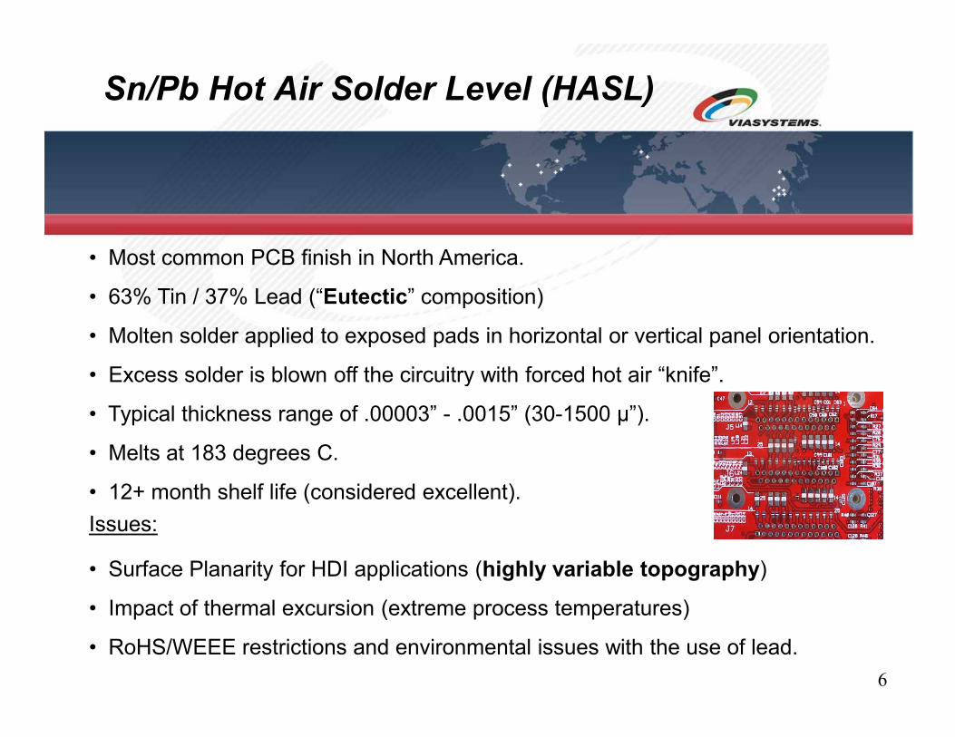
• Most common PCB finish in North America.
• 63% Tin / 37% Lead (“Eutectic” composition)
• Molten solder applied to exposed pads in horizontal or vertical panel orientation.
• Excess solder is blown off the circuitry with forced hot air “knife”.
Sn/Pb Hot Air Solder Level (HASL)
6
• Excess solder is blown off the circuitry with forced hot air “knife”.
• Typical thickness range of .00003” - .0015” (30-1500 µ”).
• Melts at 183 degrees C.
• 12+ month shelf life (considered excellent).
Issues:
• Surface Planarity for HDI applications (highly variable topography)
• Impact of thermal excursion (extreme process temperatures)
• RoHS/WEEE restrictions and environmental issues with the use of lead.
• Same application process (HASL) as Sn/Pb Solder.
• Common alloys: Sn/Ag/Cu (SAC), Sn/Cu/Co, Sn/Cu/Ni/Ge.
• Slightly more planar (uniform) coating than can be achieved with tin/lead solders.
• Typical thickness range of .0003”-.001” (300-1000 µ”).
Lead-Free Solder
7
• Typical thickness range of .0003”-.001” (300-1000 µ”).
• Melts at 228 degrees C.
• Environmentally Friendly (RoHS & WEEE compliant).
• 12 month shelf life.
Issues:
• Low demand as PCB finish (outsourced when required).
• Aggressive on copper, depending on the alloy.
• Relatively new compared to Sn/Pb solder (less history).
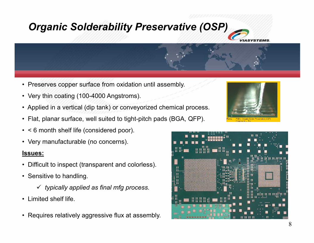
• Preserves copper surface from oxidation until assembly.
• Very thin coating (100-4000 Angstroms).
• Applied in a vertical (dip tank) or conveyorized chemical process.
• Flat, planar surface, well suited to tight-pitch pads (BGA, QFP).
Organic Solderability Preservative (OSP)
8
• Flat, planar surface, well suited to tight-pitch pads (BGA, QFP).
• < 6 month shelf life (considered poor).
• Very manufacturable (no concerns).
Issues:
• Difficult to inspect (transparent and colorless).
• Sensitive to handling.
� typically applied as final mfg process.
• Limited shelf life.
• Requires relatively aggressive flux at assembly.
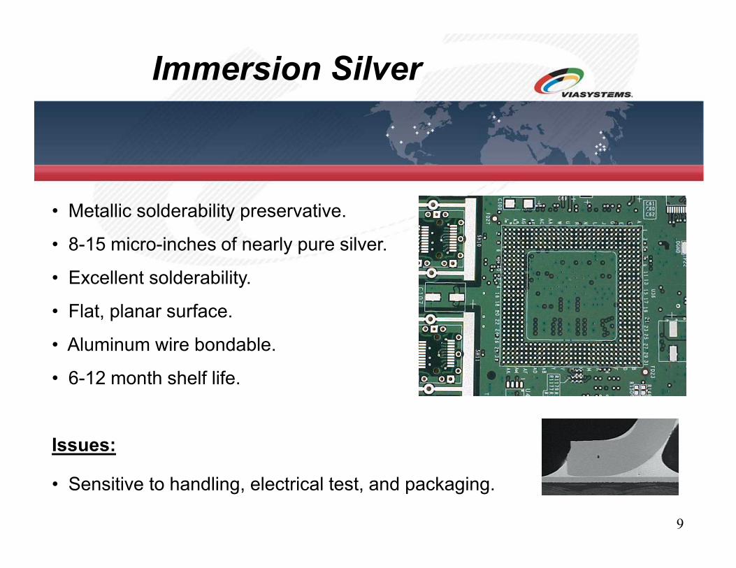
• Metallic solderability preservative.
• 8-15 micro-inches of nearly pure silver.
• Excellent solderability.
Immersion Silver
9
• Excellent solderability.
• Flat, planar surface.
• Aluminum wire bondable.
• 6-12 month shelf life.
Issues:
• Sensitive to handling, electrical test, and packaging.
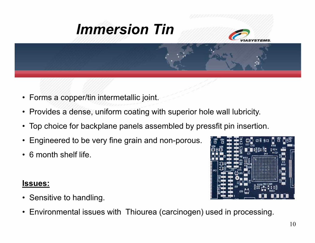
• Forms a copper/tin intermetallic joint.
• Provides a dense, uniform coating with superior hole wall lubricity.
• Top choice for backplane panels assembled by pressfit pin insertion.
Immersion Tin
10
• Top choice for backplane panels assembled by pressfit pin insertion.
• Engineered to be very fine grain and non-porous.
• 6 month shelf life.
Issues:
• Sensitive to handling.
• Environmental issues with Thiourea (carcinogen) used in processing.
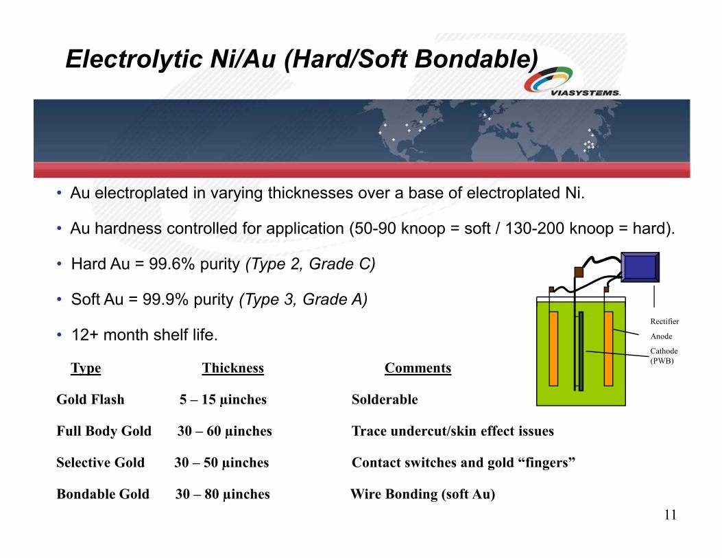
• Au electroplated in varying thicknesses over a base of electroplated Ni.
• Au hardness controlled for application (50-90 knoop = soft / 130-200 knoop = hard).
• Hard Au = 99.6% purity (Type 2, Grade C)
Electrolytic Ni/Au (Hard/Soft Bondable)
11
• Soft Au = 99.9% purity (Type 3, Grade A)
• 12+ month shelf life.
Type Thickness Comments
Gold Flash 5 – 15 µinches Solderable
Full Body Gold 30 – 60 µinches Trace undercut/skin effect issues
Selective Gold 30 – 50 µinches Contact switches and gold “fingers”
Bondable Gold 30 – 80 µinches Wire Bonding (soft Au)
Rectifier
Anode
Cathode
(PWB)

Gold
Electrolytic Ni/Au Issues/Concerns
12
Gold
Nickel
Copper
PCB Substrate
Full-Body Gold “Undercut”
(when bussing isn’t possible)
aka “Gold as Etch Resist”
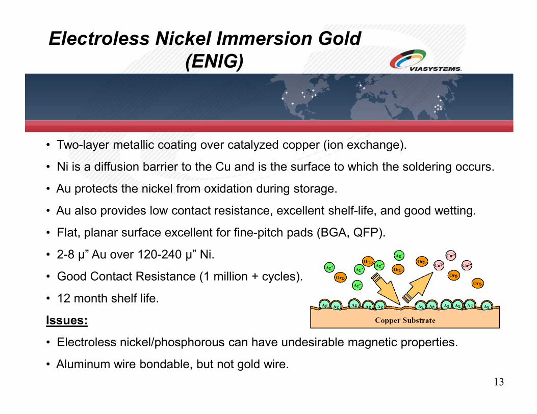
• Two-layer metallic coating over catalyzed copper (ion exchange).
• Ni is a diffusion barrier to the Cu and is the surface to which the soldering occurs.
• Au protects the nickel from oxidation during storage.
• Au also provides low contact resistance, excellent shelf-life, and good wetting.
Electroless Nickel Immersion Gold
(ENIG)
13
• Au also provides low contact resistance, excellent shelf-life, and good wetting.
• Flat, planar surface excellent for fine-pitch pads (BGA, QFP).
• 2-8 µ” Au over 120-240 µ” Ni.
• Good Contact Resistance (1 million + cycles).
• 12 month shelf life.
Issues:
• Electroless nickel/phosphorous can have undesirable magnetic properties.
• Aluminum wire bondable, but not gold wire.
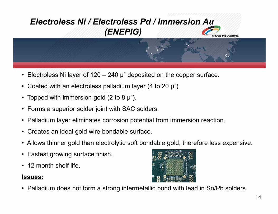
• Electroless Ni layer of 120 – 240 µ” deposited on the copper surface.
• Coated with an electroless palladium layer (4 to 20 µ”)
• Topped with immersion gold (2 to 8 µ”).
• Forms a superior solder joint with SAC solders.
Electroless Ni / Electroless Pd / Immersion Au
(ENEPIG)
14
• Forms a superior solder joint with SAC solders.
• Palladium layer eliminates corrosion potential from immersion reaction.
• Creates an ideal gold wire bondable surface.
• Allows thinner gold than electrolytic soft bondable gold, therefore less expensive.
• Fastest growing surface finish.
• 12 month shelf life.
Issues:
• Palladium does not form a strong intermetallic bond with lead in Sn/Pb solders.
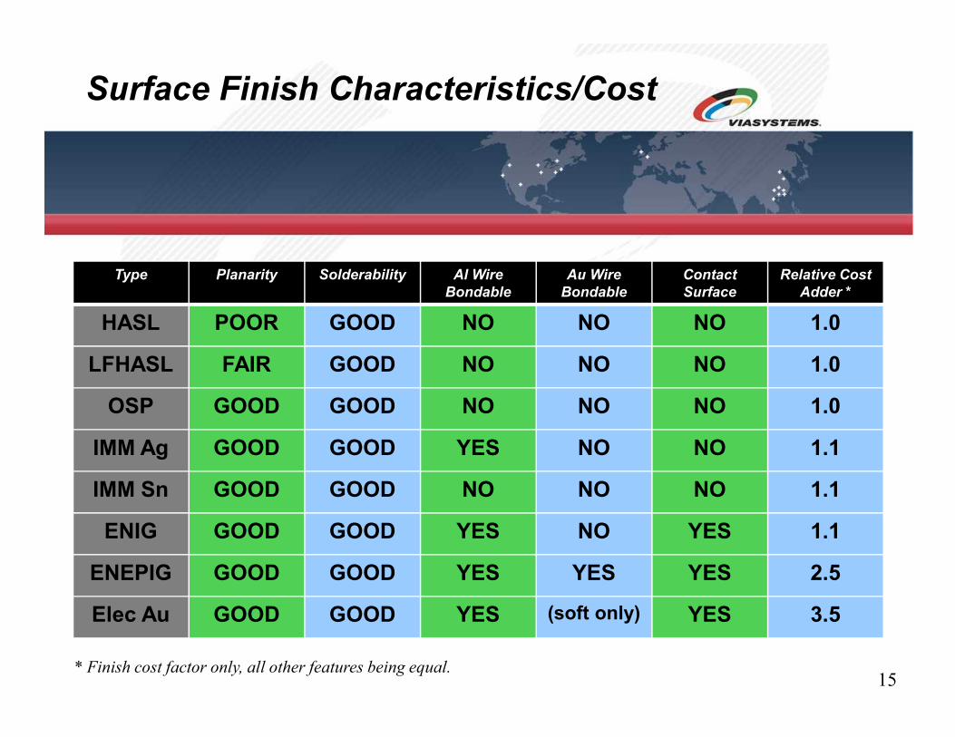
Type Planarity Solderability Al Wire
Bondable
Au Wire
Bondable
Contact
Surface
Relative Cost
Adder *
HASL POOR GOOD NO NO NO 1.0
LFHASL FAIR GOOD NO NO NO 1.0
Surface Finish Characteristics/Cost
15
LFHASL FAIR GOOD NO NO NO 1.0
OSP GOOD GOOD NO NO NO 1.0
IMM Ag GOOD GOOD YES NO NO 1.1
IMM Sn GOOD GOOD NO NO NO 1.1
ENIG GOOD GOOD YES NO YES 1.1
ENEPIG GOOD GOOD YES YES YES 2.5
Elec Au GOOD GOOD YES (soft only) YES 3.5
* Finish cost factor only, all other features being equal.
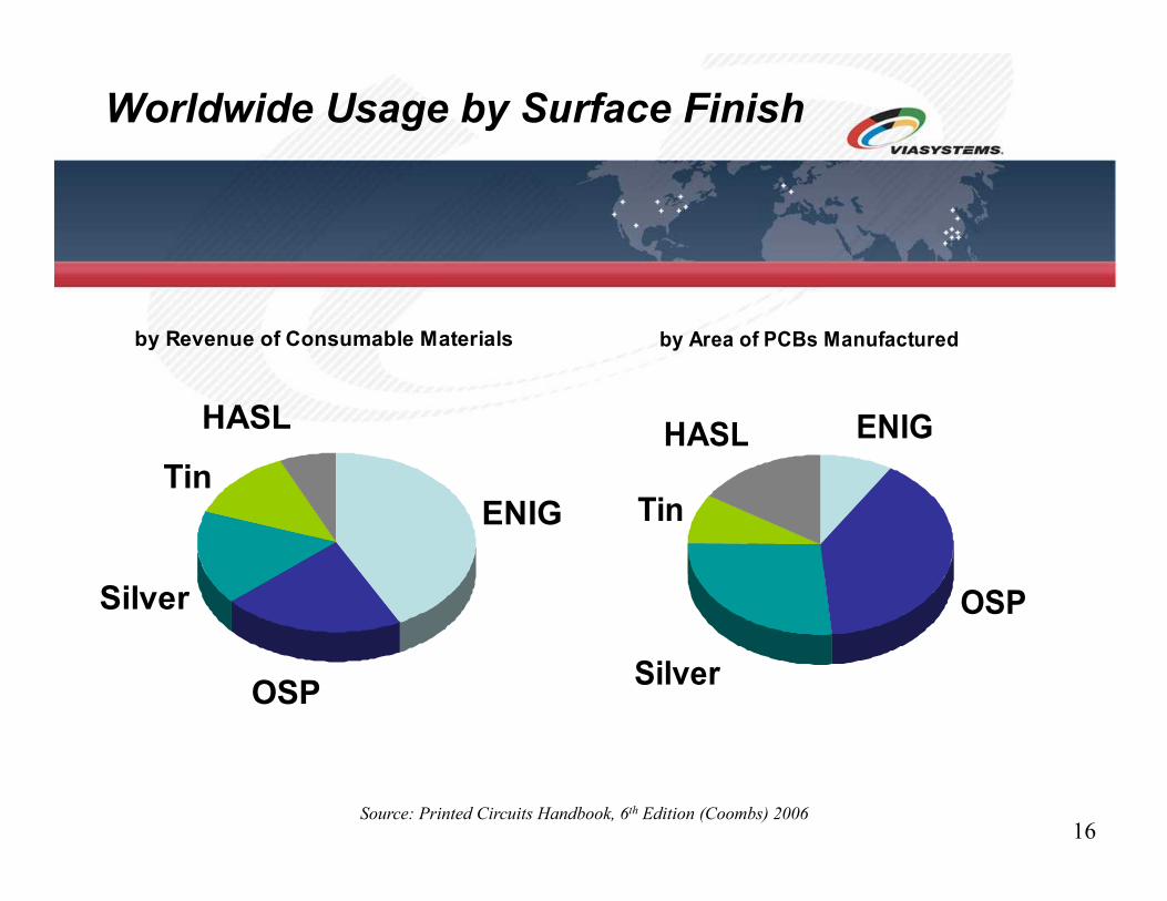
by Area of PCBs Manufactured
ENIGHASL
by Revenue of Consumable Materials
HASL
Worldwide Usage by Surface Finish
16
OSP
Silver
Tin
HASL
ENIG
OSP
Silver
Tin
Source: Printed Circuits Handbook, 6th Edition (Coombs) 2006
www.viasystems.com
17
Thank You!