The evolution of surface finishes in mobile phone … · 2004-09-16 · The evolution of surface...
10
The evolution of surface finishes in mobile phone applications. Claus Würtz Nielsen Nokia Mobile Phones R&D Frederikskaj, DK-1790 Copenhagen V, Denmark +45 20860091 Email: [email protected] Abstract During the last 5 years mobile phones and other portable consumer electronics have been extremely popular and spread all over the world in different climate zones in very high volumes. At the same time the mobile phone terminal for many people has become a necessity that is brought with them in any activity they practice. These changes in user behavior have heavily changed the impact on handheld terminals from moisture, sweat, corrosive atmospheres and mechanical drop. As a result of this the requirement to solder joint reliability, corrosion stability and wear resistance are heavily increasing to keep a high reliability of the terminal. Immersion Ni/Au has been the overall dominant surface finish on Printed Wiring Boards (PWB’s) for the last 10 years, but a paradigm shift to avoid use of this thin and porous surface finish is ongoing nowadays because it can’t address these challenges in a satisfactory way. In today’s handheld terminals, Organic Solder Preservative (OSP) has replaced Immersion Ni/Au on solder pads. Carbon surface finish for Key- and spring contact-pads, combined with the right concept design can make use of Immersion Ni/Au unnecessary in the near future. The result will be higher reliability with less expensive and simpler processes. This paper will discuss the various considerations for choice of surface finish and results from the feasibility studies performed. Keywords: Surface finish. HASL. Ni/Au. ENIG. OSP. Carbon. Reliability. Black-Pad. Inter Metallic Compound. Gold Embrittlement. Corrosion. Environmental Test. User profile. Portable consumer electronics. 1. INTRODUCTION Electroless Nickel Immersion Gold (ENIG) has been the dominant surface finish on PWB’s for the last 10 years and the ENIG process is currently standard at most PWB manufacturers in the world. It was introduced for historical reasons as an oxidation prevention layer to give good solderability wetting and enable long time storage of the PWB’s. ENIG works well from this perspective but from a reliability point of view the use of this surface should be limited as much as possible in mobile electronic equipment. Recently it has been demonstrated that specific features and phenomena as cold solder joints caused by gold-embrittlement, solder joint interface cracking, corrosion and wear out of contact pads can be directly linked to choice of ENIG as surface finish on the PWB. Therefore alternative surface finishes for both soldering and electromechanical contacts became necessary to evaluate and implement to assure high reliability of portable consumer electronics. This paper addresses the issues of surface finishes for rigid PWB’s. 2. SURFACE FINISH OPTIONS The most important drivers for selection of surface finishes are: • Reliability • Availability • Cost Before a surface finish can be selected for a specific rigid PWB it is important to consider the properties of the finish for a given application. Is it just for soldering or is it also for electromechanical contacts as e.g. keypads switches or spring connectors? There does not so far exist a single universal surface finish that can address both high reliability of solderjoints and the electromechanical contact pads for spring- loaded connectors that commonly are used in mobile phones. Surface finishes on PWB’s can be divided into 2 main groups with different basic requirements: 2.1. Surface finishes for soldering: A surface finish for soldering has to meet several requirements, namely: .
-
Upload
trinhkhanh -
Category
Documents
-
view
214 -
download
0
Transcript of The evolution of surface finishes in mobile phone … · 2004-09-16 · The evolution of surface...

The evolution of surface finishes in mobile phone applications.
Claus Würtz Nielsen Nokia Mobile Phones R&D
Frederikskaj, DK-1790 Copenhagen V, Denmark +45 20860091 Email: [email protected]
Abstract
During the last 5 years mobile phones and other portable consumer electronics have been extremely popular and spread all over the world in different climate zones in very high volumes. At the same time the mobile phone terminal for many people has become a necessity that is brought with them in any activity they practice. These changes in user behavior have heavily changed the impact on handheld terminals from moisture, sweat, corrosive atmospheres and mechanical drop. As a result of this the requirement to solder joint reliability, corrosion stability and wear resistance are heavily increasing to keep a high reliability of the terminal. Immersion Ni/Au has been the overall dominant surface finish on Printed Wiring Boards (PWB’s) for the last 10 years, but a paradigm shift to avoid use of this thin and porous surface finish is ongoing nowadays because it can’t address these challenges in a satisfactory way. In today’s handheld terminals, Organic Solder Preservative (OSP) has replaced Immersion Ni/Au on solder pads. Carbon surface finish for Key- and spring contact-pads, combined with the right concept design can make use of Immersion Ni/Au unnecessary in the near future. The result will be higher reliability with less expensive and simpler processes. This paper will discuss the various considerations for choice of surface finish and results from the feasibility studies performed.
Keywords: Surface finish. HASL. Ni/Au. ENIG. OSP. Carbon. Reliability. Black-Pad. Inter Metallic Compound. Gold Embrittlement. Corrosion. Environmental Test. User profile. Portable consumer electronics.
1. INTRODUCTION
Electroless Nickel Immersion Gold (ENIG) has been the dominant surface finish on PWB’s for the last 10 years and the ENIG process is currently standard at most PWB manufacturers in the world. It was introduced for historical reasons as an oxidation prevention layer to give good solderability wetting and enable long time storage of the PWB’s. ENIG works well from this perspective but from a reliability point of view the use of this surface should be limited as much as possible in mobile electronic equipment. Recently it has been demonstrated that specific features and phenomena as cold solder joints caused by gold-embrittlement, solder joint interface cracking, corrosion and wear out of contact pads can be directly linked to choice of ENIG as surface finish on the PWB. Therefore alternative surface finishes for both soldering and electromechanical contacts became necessary to evaluate and implement to assure high reliability of portable consumer electronics. This paper addresses the issues of surface finishes for rigid PWB’s.
2. SURFACE FINISH OPTIONS
The most important drivers for selection of surface finishes are:
• Reliability • Availability • Cost
Before a surface finish can be selected for a specific rigid PWB it is important to consider the properties of the finish for a given application. Is it just for soldering or is it also for electromechanical contacts as e.g. keypads switches or spring connectors? There does not so far exist a single universal surface finish that can address both high reliability of solderjoints and the electromechanical contact pads for spring-loaded connectors that commonly are used in mobile phones. Surface finishes on PWB’s can be divided into 2 main groups with different basic requirements: 2.1. Surface finishes for soldering:
A surface finish for soldering has to meet several requirements, namely:
.
• Superior wettability • Solder joint strength • Surface planarity for fine pitch and CSP
assembly Several options are available in the industry, some of these are:
• HASL (Hot Air Solder Leveling) • Immersion Tin • Ni/Au (ENIG) • Immersion Silver • OSP (Organic Surface Preservative) Not all options are identical in performance.
2.2. Surface finishes for electromechanical contact pads:
A surface finish for contact pads has to meet other requirements, namely:
• Mechanical durability (Wear resistance) • Corrosion stability • Contact resistance
and some of the options are:
• Ni/Au (Electroplated) • Ni/Au (ENIG) • Immersion Silver • Carbon • Solder paste (Sn/Sn contact)
2.3. Summary of options
When one examines the surface finishes that actually have been used in various kinds of portable electronic equipment during the last 20 years, it does not seem logical why ENIG became as popular, and other finishes were almost disregarded for many years:
• One part of the explanation is, of course, that the knowledge about failure mechanisms we have today was not available until recently. They have been revealed as our experience increased.
• The other part is a reluctance to change of traditions in the electronic industry, even after analytical labs and reliability specialists have addressed the problems.
• The last part is that lack of surface finish physical availability at PWB manufacturers always will delay a change to other finishes. Investments in ENIG processes have been made and setting up new equipment for other finishes require more investments. This fact also creates certain delay.
An overview of the events that have had influence on change of surface finishes is given in the following paragraph. 3. HISTORICAL EVOLUTION OF PWB SURFACE FINISHES IN MOBILE PHONES:
3.1. HASL + Carbon
In 1st generation products from late 80-ties the normal surface finish for pads on PWB’s was HASL. HASL was in many cases combined with use of Carbon as finish for Key- and LCD-pads. Surface Mount Component technology was in its early stage and gull-wing type components had leads with relatively large pitch (1,27 mm). In beginning of the 90-ties the need for more I/O’s demanded new packages and QFP’s were introduced. The pitch decreased to 0.6 mm and a lot of solder bridging occurred because of the uneven thickLow manufacturing yield dto be replaced. 3.2. Electroless Nickel (ENIG)
The only way out of the panother solderable surface coplanar surface. Bare acceptable because of osolderability (wetting). OSP was not for discussiothough the technology existENIG was selected to beHASL. The perception at tuniversal surface finish forkeypads was found. Carbon was therefore nonecessary and removed technical problems existedwas acceptable. For a period the ENIG worked very well but then mless space was needed sobsolete and was replaced(BGA) and Chip Scale packages. The BGA packages (Fig. 3) also gave some new challenges. Smaller solder pads were introduced contemporary w
.
Fig. 1: SO Package
Fig. 2: QFP Package
ness of the HASL. emanded the HASL
Immersion Gold
roblem was to find finish with a flat and Copper was not
xidation impact on
n at that time even ed! the successor for hat time was that a both soldering and
more regarded as even though no
and the reliability
process in general ore functionality at
o the QFP became by Ball Grid Array
Fig. 3: BGA Package
ith an increase of

volume production as big as never before in electronic industry. Running PWB manufacturing in extreme high volumes means that any weakness of the process becomes a lot clearer, and serious. 3.2.1. Black Pad
A problem called Black pads occurred randomly at different PWB suppliers even though they used different brands of the Ni/Au process. The impact of missing gold on randomly single pads is poor or non-wetting, resulting in missing interconnections. Mostly they were found and rejected at the phone assembly line but worst-case scenario was if a unit passed 100% electrical test and later failed in field. A random error could be the result and the phone had a malfunction if the PWB was bent just as much as the poor solderjoint lost connection.
Fig. 4: Black Pad
There have been many theories why black pads appear but no real agreement about what is the trigger. However the bath manufacturers have made some progress in this area during the years, the ENIG process still can’t get rid of this failure type, which in some cases may be PWB design related. 3.2.2. Solder ball interfacial cracking
In connection with the Black Pad problem a new failure type called interfacial degradation was revealed. Micro sections of failing BGA or CSP components showed cracks in the interface between the Cu pad and the solder ball even though the solder wetting had been fine (Fig. 5). What could be the reason for that? After a lot of investigation it was found to be a combination of three things:
• An overlooked problem with brittle Inter Metallic Compound (IMC) between Nickel and Tin.
• The fact that users started to drop the products on the ground a lot more than earlier.
• Lack of solder joint stress relief in the rigid BGA package type compared to that of the older package types.
BGA solder ball
Crack at the PWB land/solder interface
Cu
Fig. 5: Solder ball interface cracking
IMC problem: During the soldering process a brittle nickel-tin IMC is formed. When the product is exposed to mechanical shock it then can lead to fractures of the IMC’s in the solderjoints on especially BGA-type components (Fig. 6). The phenomenon is known as the “gold-embrittlement” and had obviously existed since ENIG was introduced.
Fig. 6: Brittle fracture of IMC in a solderjoint
Package stress: The QFP’s do have gull-wing type leads that give adequate stress relief to the solderjoint to withstand some level of mechanical stress. The stiff BGA packages with balls (Fig. 7) do not give much stress relief of importance when the PWB is bended during drop of the phone. Therefore the threshold limit for initiating a crack in the IMC is easily exceeded.
Fig. 7: PWB bending during drop of phone
.
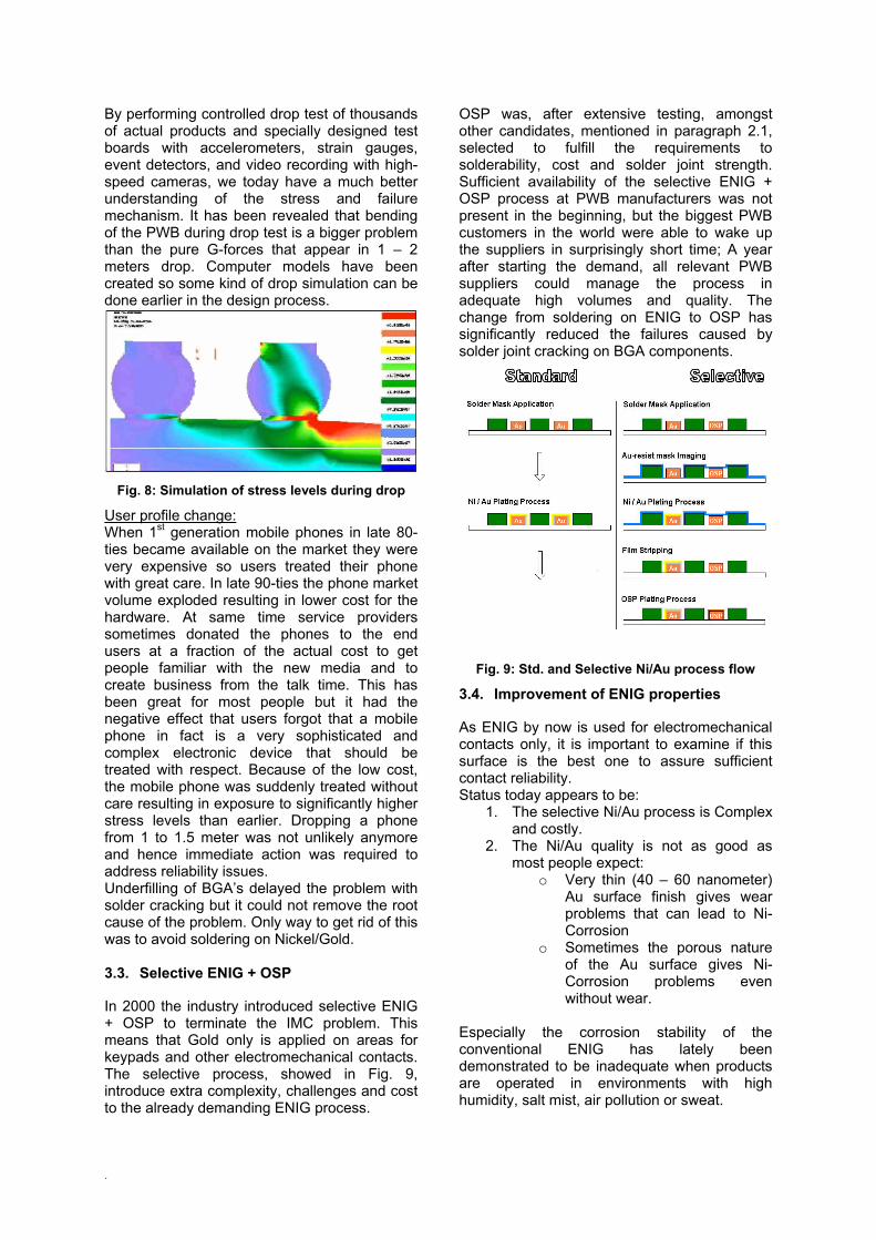
By performing controlled drop test of thousands of actual products and specially designed test boards with accelerometers, strain gauges, event detectors, and video recording with high-speed cameras, we today have a much better understanding of the stress and failure mechanism. It has been revealed that bending of the PWB during drop test is a bigger problem than the pure G-forces that appear in 1 – 2 meters drop. Computer models have been created so some kind of drop simulation can be done earlier in the design process.
Fig. 8: Simulation of stress levels during drop
User profile change: When 1st generation mobile phones in late 80-ties became available on the market they were very expensive so users treated their phone with great care. In late 90-ties the phone market volume exploded resulting in lower cost for the hardware. At same time service providers sometimes donated the phones to the end users at a fraction of the actual cost to get people familiar with the new media and to create business from the talk time. This has been great for most people but it had the negative effect that users forgot that a mobile phone in fact is a very sophisticated and complex electronic device that should be treated with respect. Because of the low cost, the mobile phone was suddenly treated without care resulting in exposure to significantly higher stress levels than earlier. Dropping a phone from 1 to 1.5 meter was not unlikely anymore and hence immediate action was required to address reliability issues. Underfilling of BGA’s delayed the problem with solder cracking but it could not remove the root cause of the problem. Only way to get rid of this was to avoid soldering on Nickel/Gold. 3.3. Selective ENIG + OSP
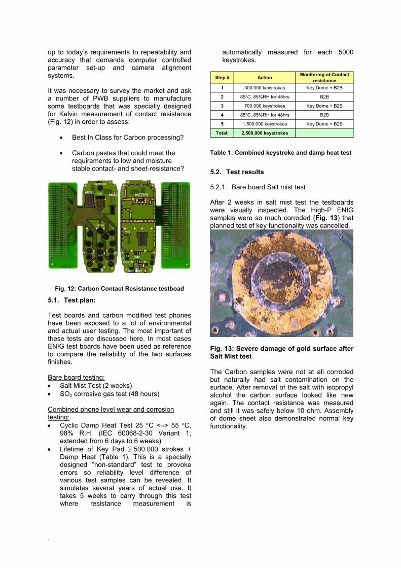
In 2000 the industry introduced selective ENIG + OSP to terminate the IMC problem. This means that Gold only is applied on areas for keypads and other electromechanical contacts. The selective process, showed in Fig. 9, introduce extra complexity, challenges and cost to the already demanding ENIG process.
OSP was, after extensive testing, amongst other candidates, mentioned in paragraph 2.1, selected to fulfill the requirements to solderability, cost and solder joint strength. Sufficient availability of the selective ENIG + OSP process at PWB manufacturers was not present in the beginning, but the biggest PWB customers in the world were able to wake up the suppliers in surprisingly short time; A year after starting the demand, all relevant PWB suppliers could manage the process in adequate high volumes and quality. The change from soldering on ENIG to OSP has significantly reduced the failures caused by solder joint cracking on BGA components.
Fig. 9: Std. and Selective Ni/Au process flow
3.4. Improvement of ENIG properties
As ENIG by now is used for electromechanical contacts only, it is important to examine if this surface is the best one to assure sufficient contact reliability. Status today appears to be:
1. The selective Ni/Au process is Complex and costly.
2. The Ni/Au quality is not as good as most people expect:
o Very thin (40 – 60 nanometer) Au surface finish gives wear problems that can lead to Ni-Corrosion
o Sometimes the porous nature of the Au surface gives Ni-Corrosion problems even without wear.
Especially the corrosion stability of the conventional ENIG has lately been demonstrated to be inadequate when products are operated in environments with high humidity, salt mist, air pollution or sweat.
.

As a result of this the formulation of the Ni process recently has been adjusted (mainly P content) with the effect that the Ni surface becomes slightly superior and that the Immersion Au on top becomes less porous. The end result is that corrosion stability with the modified High P ENIG has been improved to a higher level if the thin Au surface is not damaged by scratches or wear. In spite of the improvement the immersion gold processes can never give a totally pore free surface as is the case for electroplated gold. It becomes more and more clear that the thin ENIG in the future not will be able to address the need for higher wear resistance in the extreme part of the product segments as gaming devices and phones used by workmen or during sport activities. Therefore it’s important to consider replacing the ENIG with something more reliable. 4. RECONSIDERATION OF FINISHES FOR CONTACTS
The following candidates have been studied: • Ni/Au (Electroplated) • Ni/Au (Electroplated on P3 for
assembly) • Carbon (Screen-printed)
4.1. Electroplated gold on rigid PWB’s
Electroplating of the PWB with Nickel/Gold (hard-gold, thicker than 0.8 um) is the technically most attractive contact surface because of low contact resistance, fine durability and corrosion properties, but the very high cost for this process disqualifies it in most cases. Another practical hindering for use is that short-circuiting of all pads is needed during the plating process with bus bars. After plating, the busbars must be opened resulting in long “dead traces” that is a nightmare for Electro Magnetic Compatibility and Electro Static Discharge properties. Only in rare cases where all relevant pads are placed in the perimeter of the PWB it makes sense, and the busbar then can be removed effectively and easy during the routing process.
4.2. Electroplated gold on P3
Pick and Place Pads (P3) are small pieces of metal foil made of Cu or Nickel-silver. The P3 are electroplated with solid layers of Ni and Au. P3 components can easily be designed in any needed shape, size and thickness and handled as a resistor or capacitor for easy assembly. By use of P3 it is possible to place and Reflow-solder high quality gold contact points
anywhere needed on the PWB. The PWB then just needs one solderable surface finish as e.g. OSP or Immersion Silver. Cost wise a solution with P3 on OSP is attractive compared to selective ENIG + OSP if number of P3 is limited to < 10 pcs. Only for keypads the P3 is not a feasible solution. Therefore, another surface finish is still needed. Carbon is considered the most obvious choice for keypads. 4.3. Carbon on rigid PWB’s
Carbon has widely been used in PWB industry for more than 30 years, but for the last 10+ years it has been in obscurity. From a highly appreciated use on rigid boards in the 70-ties and 80-ties carbon was almost out-competed by the ENIG in the 90-ties. Only applications as keyboards on remote controls, calculators, walkie-talkies and different kind of electronic toys have continuously used this surface on rigid boards until today. In addition to this, membrane touch switch keyboards based on polyester flex with polymer Silver and Carbon are still widely used. Only the high-end and mobile device market has in general disregarded carbon as an option on Rigid PWB’s. This is anomalous when one considers the advantages the Carbon surface offers:
• Simple and cheap process. (Fig. 10) • High corrosion resistance to O2, SO2,
NOx, Cl- and other gases. • Almost no impact from liquids as e.g.:
most solvents, coffee, beer, coke etc. • Good wear resistance (Thick and ”self
lubricating” surface). • More environmental friendly process
than the ENIG process. The disadvantages are a few but important to be aware of:
• High contact resistance compared to pure metallic surfaces. Typically from 4 – 10 ohm.
• Placement tolerance of carbon layer is typically +/- 150 um.
• As Carbon paste by nature is more or less hygroscopic it’s important only to use best in class materials cured in a proper way. If inadequate materials or heat curing profiles are used the resistance will be moisture sensitive.
4.3.1. Manufacturing process
Carbon is applied as an additive process (Fig. 10) by screen-printing. It is a relatively simple
.

process involving significantly fewer steps and process chemicals compared to the ENIG process.
Solder Mask Application Process |
1) Cu-surface Deoxidation |
2) Carbon paste Screen Printing |
3) Carbon Paste Curing
(If C on both sides: repeat step 1 - 3) |
OSP Process
Fig. 10: Carbon process flow
Infrared curing of the Carbon has in earlier studies [1] and [2] been demonstrated to give a noticeable improvement of resistance stability and welcomed decrease of Sheet resistance. If Infrared curing is performed with optimum profile and automatic in-line equipment, the total process time for all three steps can be as low as 15 minutes and hence very suitable for mass volume production. 4.3.2. Contact resistance
Contact resistance is defined as the resistance between an electromechanical contact and the Copper in the PWB. This resistance is a total of:
1. Spring-contact to carbon interface resistance
2. Carbon thickness bulk resistance 3. Carbon to Copper interface resistance
A controlled and stable level of contact resistance is a simple requirement for the success of Carbon technology. A contact resistance level of 5 ohm is easily obtainable when using right materials and process. Contact resistance >10 should not be accepted because it indicates problems in the manufacturing process. Typically a high contact resistance will indicate an inadequate deoxidation of the copper surface prior to the carbon screen-printing process. A very simple way to judge if the Carbon manufacturing process has been performed in the right way is to expose the samples to Damp heat test. If contact resistance after 2 days in 85 °C, 85 % R.H. gives a significant and permanent increase of the contact resistance exceeding 10 ohm, then the process has been out of control. (See example of this in Fig. 15, Supplier E).
4.3.3. Carbon sheet resistivity
To complete the picture about Carbon it is necessary to mention that some of the emergent embedded resistor technologies are based on polymer Carbon resistors. In principle these resistor materials are similar to the Carbon for surface finishes. Difference is mostly that the sheet resistance is adjusted to fit each decade as e.g. 100 ohm/square, 1Kohm/sq, 10Kohm/sq. etc. Sheet resistivity for “Contact-Carbon” should be as low as possible: Typ. 15 ohm/sq and max 25 ohm/sq. 4.4. The ideal combination
Potentially the following combination could be the cost/reliability wise most attractive and flexible solution for the future:
• OSP for solder pads. • Potentially Imm. Ag for solder pads. • Soldered connectors or P3 for the
contact resistance critical electromechanical connections.
• Carbon for keypads and the other less resistance critical electromechanical contact pads.
One of the challenges for this combination was qualification testing of the Carbon technology on the premises that exist in today’s portable terminals. Following section describes some of the results from the testing carried out.
P3
Carbon
Fig. 11: P3 and C-pads on PWB for spring connectors
5. RELIABILITY TESTING OF CARBON
As Carbon had been widely disregarded by the electronic industry for the last 10+ years it was a fact that most PWB manufacturers had to revisit the process skills they possessed in the past. Screen-printing machines were not always
.
up to today’s requirements to repeatability and accuracy that demands computer controlled parameter set-up and camera alignment systems.
It was necessary to survey the market and ask a number of PWB suppliers to manufacture some testboards that was specially designed for Kelvin measurement of contact resistance (Fig. 12) in order to assess:
• Best In Class for Carbon processing?
• Carbon pastes that could meet the requirements to low and moisture stable contact- and sheet-resistance?
Fig. 12: Carbon Contact Resistance testboad
5.1. Test plan:
Test boards and carbon modified test phones have been exposed to a lot of environmental and actual user testing. The most important of these tests are discussed here. In most cases ENIG test boards have been used as reference to compare the reliability of the two surfaces finishes. Bare board testing: • Salt Mist Test (2 weeks) • SO2 corrosive gas test (48 hours) Combined phone level wear and corrosion testing: • Cyclic Damp Heat Test 25 °C <–> 55 °C,
98% R.H. (IEC 60068-2-30 Variant 1, extended from 6 days to 6 weeks)
• Lifetime of Key Pad 2.500.000 strokes + Damp Heat (Table 1). This is a specially designed “non-standard” test to provoke errors so reliability level difference of various test samples can be revealed. It simulates several years of actual use. It takes 5 weeks to carry through this test where resistance measurement is
automatically measured for each 5000 keystrokes.
Step # Action Monitoring of Contact
resistance1 300.000 keystrokes Key Dome + B2B
2 85°C, 85%RH for 48hrs B2B
3 700.000 keystrokes Key Dome + B2B
4 85°C, 85%RH for 48hrs B2B
5 1.500.000 keystrokes Key Dome + B2B
Total: 2.500.000 keystrokes
Table 1: Combined keystroke and damp heat test
5.2. Test results
5.2.1. Bare board Salt mist test
After 2 weeks in salt mist test the testboards were visually inspected. The High-P ENIG samples were so much corroded (Fig. 13) that planned test of key functionality was cancelled.
Fig. 13: Severe damage of gold surface after Salt Mist test The Carbon samples were not at all corroded but naturally had salt contamination on the surface. After removal of the salt with isopropyl alcohol the carbon surface looked like new again. The contact resistance was measured and still it was safely below 10 ohm. Assembly of dome sheet also demonstrated normal key functionality.
.
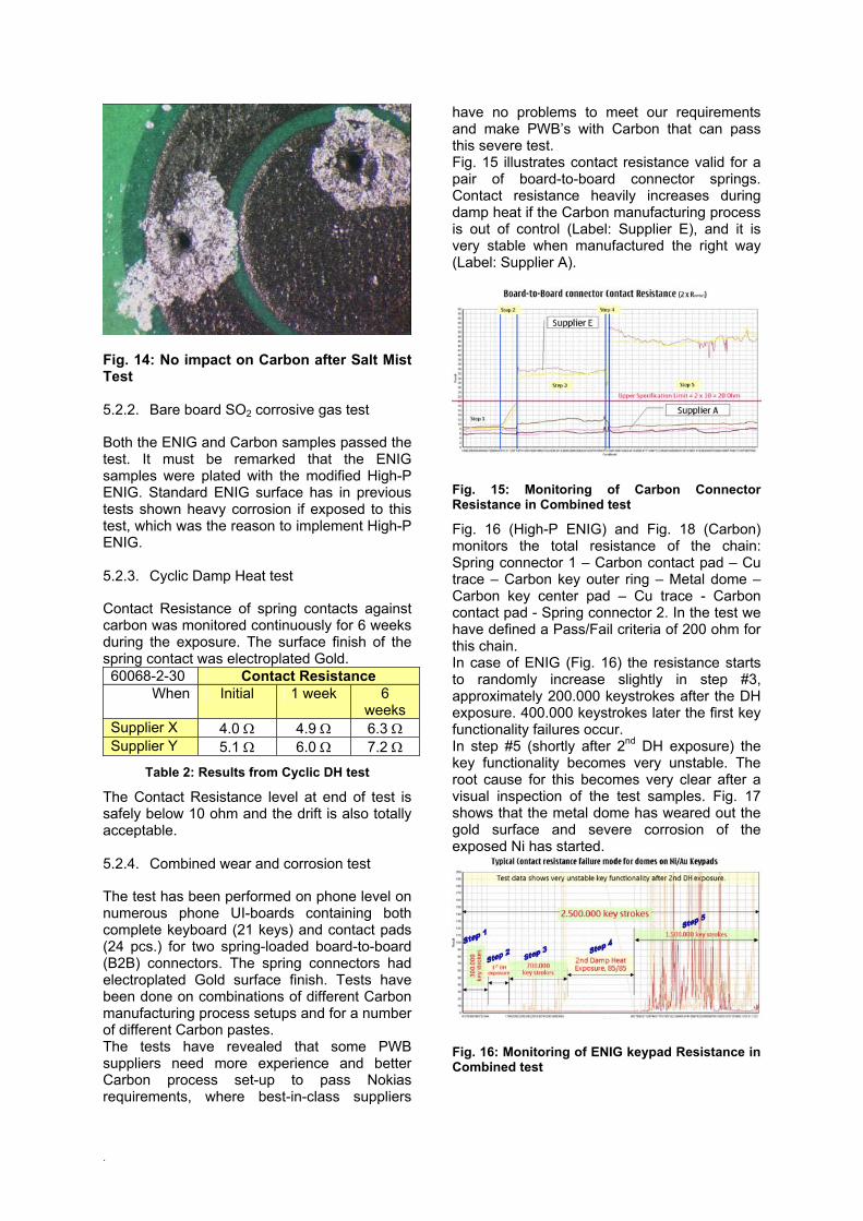
Fig. 14: No impact on Carbon after Salt Mist Test 5.2.2. Bare board SO2 corrosive gas test
Both the ENIG and Carbon samples passed the test. It must be remarked that the ENIG samples were plated with the modified High-P ENIG. Standard ENIG surface has in previous tests shown heavy corrosion if exposed to this test, which was the reason to implement High-P ENIG. 5.2.3. Cyclic Damp Heat test
Contact Resistance of spring contacts against carbon was monitored continuously for 6 weeks during the exposure. The surface finish of the spring contact was electroplated Gold. 60068-2-30 Contact Resistance
When Initial 1 week 6 weeks
Supplier X 4.0 Ω 4.9 Ω 6.3 Ω Supplier Y 5.1 Ω 6.0 Ω 7.2 Ω
Table 2: Results from Cyclic DH test
The Contact Resistance level at end of test is safely below 10 ohm and the drift is also totally acceptable. 5.2.4. Combined wear and corrosion test
The test has been performed on phone level on numerous phone UI-boards containing both complete keyboard (21 keys) and contact pads (24 pcs.) for two spring-loaded board-to-board (B2B) connectors. The spring connectors had electroplated Gold surface finish. Tests have been done on combinations of different Carbon manufacturing process setups and for a number of different Carbon pastes. The tests have revealed that some PWB suppliers need more experience and better Carbon process set-up to pass Nokias requirements, where best-in-class suppliers
have no problems to meet our requirements and make PWB’s with Carbon that can pass this severe test. Fig. 15 illustrates contact resistance valid for a pair of board-to-board connector springs. Contact resistance heavily increases during damp heat if the Carbon manufacturing process is out of control (Label: Supplier E), and it is very stable when manufactured the right way (Label: Supplier A).
Fig. 15: Monitoring of Carbon Connector Resistance in Combined test
Fig. 16 (High-P ENIG) and Fig. 18 (Carbon) monitors the total resistance of the chain: Spring connector 1 – Carbon contact pad – Cu trace – Carbon key outer ring – Metal dome – Carbon key center pad – Cu trace - Carbon contact pad - Spring connector 2. In the test we have defined a Pass/Fail criteria of 200 ohm for this chain. In case of ENIG (Fig. 16) the resistance starts to randomly increase slightly in step #3, approximately 200.000 keystrokes after the DH exposure. 400.000 keystrokes later the first key functionality failures occur. In step #5 (shortly after 2nd DH exposure) the key functionality becomes very unstable. The root cause for this becomes very clear after a visual inspection of the test samples. Fig. 17 shows that the metal dome has weared out the gold surface and severe corrosion of the exposed Ni has started.
Fig. 16: Monitoring of ENIG keypad Resistance in Combined test
.

Fig. 17: Severe wear and corrosion of ENIG after combined test
In case of Carbon (Fig. 18) the resistance increases from 13 ohm to a level around 80 ohm (Fig. 18). This change is totally acceptable and safely below the max 200 ohm requirement. No single key-failure was detected during the entire 2.500.000 keystrokes.
Fig. 18: Monitoring of Carbon keypad Resistance in Combined test
Visual inspection of the test samples gives an amazing experience: The Carbon surface is totally intact and without any signs of corrosion (Fig. 19). Only with special lighting setup it’s possible to detect where the domes has been in contact with the Carbon.
Fig. 19: Carbon keypad not affected by combined test
5.2.5. Extreme testing of lifetime
Encouraged by the good result the combined wear and corrosion test was repeated on 36 of the samples so the total impact was 5.000.000 keystrokes and 4 DH cycles. Resistance was still below 100 ohm and the Carbon surface was still totally intact and without any signs of corrosion. 5.2.6. Extreme testing of corrosion and lifetime
Following combination test has been carried out on 18 samples of UI-boards described in 5.2.4 with Carbon + OSP:
1. 1 week Salt Mist exposure of PWB. 2. Removal of salt contamination with
isopropyl alcohol. 3. Lead-free Reflow soldering profile
exposure. 4. Assembly of dome-sheet and phone
mechanics. 5. Exposure to the Combined wear and
corrosion test with 2.500.000 keystrokes.
All samples worked perfect after assembly and passed step #1, #2 and #3 (1.000.000 keystrokes and one DH cycle) without failures. After step #4, 3 out of the 18 samples had few random key failures immediately after 2nd DH exposure. After a while in step #5, 2 of the failing samples worked fine again. Result at end of the test:
o 17 out of the 18 samples had normal key functionality.
6. CONCLUSION
Specially in mobile electronic equipment the selection of right surface finish on the PWB should be offered a lot more attention than normally done today as there do not exist a single universal surface finish that can address high reliability of both solderjoints and electromechanical contact points. 6.1. Finish for soldering:
Soldering on ENIG is not recommended in general and should be banned for BGA component types. Replacement of ENIG with OSP on PWB solderpads has with evidence from manufacturing and field feedback from tenth of millions of phones demonstrated a significant reduction of failures caused by solder joint interface cracking on BGA components.
.

OSP was originally introduced when using Sn/Pb solder but is has been able to fulfill requirements for good solderjoints also with leadfree solders. Immersion Ag could still be considered as supplement to OSP in the future. 6.2. Finish for contact pads:
Electroplated gold (thicker than 0.8 um) is a reliable choice but not always design and process compatible and available in rigid PWB industry. Unfortunately it is an expensive process and out of range for high volume low cost products. In flex PWB industry Electroplated gold is more or less a std. process but these flexes are normally expensive anyway and mostly for high end products. Pick and Place Pads electroplated with gold are a cheaper and attractive alternative to gold plated on the PWB in case of few contact points that need very low and reliable contact resistance. In this case the PWB just need OSP. Carbon provides superior reliability to ENIG on KeyPads and most Spring Contact pads where up to 10 ohm contact resistance can be accepted. Carbon is the cheapest available contact surface finish today that possesses very high corrosion resistance and good wear resistance. 6.3. Finish for ESD and cosmetic areas:
The only aspect where ENIG don’t have too much impact on reliability is on ESD and cosmetic areas. ENIG looks good when it’s new and treated with care. It gives an Impression of luxury and prestige but this dream picture quickly fade away if you have seen equipment disassembled after use in harsh environments. This kind of environment is today quite common for every day use of mobile terminals. 6.4. Summary
In the early design stage of portable electronics it’s important to carefully consider and select the PWB surface finishes used. The main factors that influence this choice are: Type, material and shape of the contacting devices, available technologies and available processes. Only by taking all these factors into consideration is it possible to fulfill the requirements to reliability expected by the end-users in a dynamic and ever changing market. A choice of surface finish that was right some time back in history may not be the right choice today. The preconditions valid at that time may have changed:
• Hardware related: o New package types. o New solder alloys. o New electromechanical connector
contact materials. o New mechanical design o Robustness of supporting
mechanics.
• End-user profile related: o Exposure to humid and corrosive
atmospheres, rain, liquids. o Exposure to vibration, drop,
number of keystrokes. o Time of direct use by user per day:
5 minutes. 1 hour. 8 hours. 24 hours.
• Technology evolution and expert
knowledge level: o Existence of new surface finishes. o Improvement of material properties
of old surface finishes. o Improvement of manufacturing
processes and equipment. o Increased knowledge about failure
mechanisms. All of these conditions, alone or in combination makes it obvious that it’s necessary to reconsider if next new product should have same PWB surface finish as usual. You cannot rely on traditional design methods in a constant changing market! 7. ACKNOWLEDGMENTS
Comments, suggestions and background information given by Viswam Puligandla and Arni Kujala are gratefully acknowledged. 8. REFERENCES
[1] Claus W. Nielsen. Title: “PTF, An attractive supplement to traditional thickfilm and PCB Technology”, 28th ISHM-Nordic Conference 1990, Finland
[2] Claus W. Nielsen. Title: “Results from the PTF research project PC2B at a-s Elbau”. 24th ISHM-Nordic Conference 1986, Finland.
[3] Leif Halbo: “Polymer Thick Film Technology, Design Guidelines and applications” ISBN 82-992193 (1990)
.