VC0338BSMA English Datasheet V1 - Canaan · PDF file9 SCK I, PD Serial clock ... 21 VDD P 0.9V...
15
A3222Q56-141012-V03-EN A3222-Q56 SHA256 Processor Datasheet Version 0.3 October 12 th , 2014 Notes1: The information is subject to change without notice. Before using this document, please confirm that this is the latest version. Notes2: Not all products and/or types are available in every country. Please check with sales representative for availability and additional information. Copyright 2012-2014 Avalon Project 2014-10-12 Page 1 of 14
Transcript of VC0338BSMA English Datasheet V1 - Canaan · PDF file9 SCK I, PD Serial clock ... 21 VDD P 0.9V...

A3222Q56-141012-V03-EN
A3222-Q56
SHA256 Processor
Datasheet
Version 0.3
October 12th, 2014
Notes1: The information is subject to change without notice. Before using this document, please confirm that this is the latest version. Notes2: Not all products and/or types are available in every country. Please check with sales representative for availability and additional information.
Copyright 2012-2014 Avalon Project 2014-10-12 Page 1 of 14

A3222Q56-141012-V03-EN
Copyright 2012-2014 Avalon Project 2014-10-12 Page 2 of 14
Table of Content
1. GENERAL DESCRIPTION ......................................................... 3
2. SYSTEM ARCHITECTURE ......................................................... 3
3. DATA INTERFACE .............................................................. 4
3.1 COMMUNICATION PROTOCOL ....................................................... 4
3.2 COMMUNICATION PORT .......................................................... 4
4. DATA FORMAT ................................................................. 6
4.1 CLOCK CONFIGURATION SEGMENT ................................................... 6
4.2 HASH DATA SEGMENT........................................................... 7
4.3 RECEIVE NONCE .............................................................. 8
5. PIN ASSIGNMENTS ............................................................. 8
5.1 SYSTEM CONTROL ............................................................. 8
5.2 FUNCTION .................................................................. 9
5.3 POWER SUPPLY .............................................................. 9
5.4 A3222Q56 PIN-PAD MAP ...................................................... 10
6. ELECTRICAL CHARACTERISTICS ................................................. 11
6.1 RECOMMENDED OPERATING CONDITIONS ............................................. 11
6.2 OSCILLATION ............................................................. 11
7. PACKAGE INFORMATION ........................................................ 12
7.1 A3222Q56 PACKAGE SPECIFICATIONS .............................................. 12
8. REVISION HISTORY ........................................................... 15

A3222Q56-141012-V03-EN
Copyright 2012-2014 Avalon Project 2014-10-12 Page 3 of 14
1. GENERAL DESCRIPTION
A3222Q56 is the fourth generation SHA256 Processor designed by AVALON team,
comes with higher hash speed and performance per watt. The major applications
for this chip is provide a chip level solution for SHA256 related work.
Features
Communication protocol compatible with the serial peripheral interface (SPI).
Support chain-mode, drastically reduced controller I/O port requirement.
More efficient clock strategy.
Efficient data transfer with two levels of frame buffer.
2. SYSTEM ARCHITECTURE
Figure 2-1 Chip Architecture
CPM SHA256-Array
SCK
CFG UNIT
MOSI
MISO
LOAD
SCKOUT
MOSIOUT
MISOIN
LOADOUT
VDD
VSS

A3222Q56-141012-V03-EN
Copyright 2012-2014 Avalon Project 2014-10-12 Page 4 of 14
3. DATA INTERFACE
3.1 Communication Protocol A3222Q56 interface supports SPI mode0: CPOL = 0, CPHA = 0. Input data is
latched in on the rising edge of SCK, and output data is available from the
falling edge of SCK.
When the bus master is in standby mode: SCK remains at 0 for (CPOL = 0, CPHA =
0 Mode 0). All timing diagrams shown in this data sheet are mode 0.
3.2 Communication Port A3222Q56 uses 2 pairs of communication ports to receive configurations and
transmit the configurations to the chip at next stage and send out the calculation
result, details are listed in Table 3-1.
Figure 3-1 A3222Q56 Communication Topology
A3222Q56
SCK
MOSI
MISO
LOAD
SCKOUT
MOSIOUT
MISOIN
LOADOUT
Former stage
Next stage
Table 3-1 A3222Q56 Communication Port, former stage/next stage
PIN NAME FUNCTION LOAD/LOADOUT End of frame. When LOAD goes LOW, the device is placed in active
mode. When LOAD is HIGH, the device is placed in inactive mode. Note: While LOAD is HIGH, Still need to send at least 8 SCK (unlike the mode 0). PINS: LOAD: from former state. LOADOUT: to next stage.
MISO/MISOIN Send out the golden nonce when A3222Q56 get the share. Data is placed on MISO at the falling edge of SCK. PINS: MISO: to former stage. MISOIN: from next stage.
MOSI/MOSIOUT Receive configurations from controller or another A3222Q56 chip. Data is placed on MISO at the falling edge of SCK.

A3222Q56-141012-V03-EN
Copyright 2012-2014 Avalon Project 2014-10-12 Page 5 of 14
PINS: MOSI: from former stage. MOSIOUT: to next stage.
SCK/SCKOUT Serial clock provides interface timing for the chip. PINS: SCK: from former stage. SCKOUT: to next stage.
Figure 3-2 A3222Q56 Communication Example
>= 8 SCK
MSB LSBX X
SCK
LOAD
MOSI
MSB LSBMISO
>= 8 SCK
MSB LSBX X
SCK
LOAD
MOSI
MSB LSBMISO
MOSI: work nMISO: work n-2 nonce
MOSI: work n+1MISO: work n-1 nonce
>= 8 SCK
MSB LSBX X
SCK
LOAD
MOSI
MSB LSBMISO
MOSI: work n+2MISO: work n nonce
Sent Work n
Sent Work n+1
Sent Work n+2
Sent Work n-1

A3222Q56-141012-V03-EN
Copyright 2012-2014 Avalon Project 2014-10-12 Page 6 of 14
NOTE: (1) While LODE is HIGH, Still need to send at least 8 SCK (unlike the mode 0). (2) A A3222Q56-work frame is 736bits. (3) The current report is twice the previous work.
ie: MISO(n) = SHA256(MOSI(n-2)).
4. DATA FORMAT
Three segments should be configured before A3222Q56 hash calculation by MISO.
Clock configuration segment is for adjusting clock frequency, gating core clock or
switching clock source. Hash data segment is the initial input data of SHA256
HASH. Hash work of chips in the same chain is split by the initial nonce segment.
Configure data should send as the order shown in Figure 4-1
Figure 4-1 A3222Q56 Configure Sequence
InitialNonce[31:0]
Hash Data[543:0] Work ID[63:0]Clock
Configuration 1[31:0]
First word Last word
ClockConfiguration 2
[31:0]
ClockConfiguration 0
[31:0]MOSI
When A3222Q56 get nonce, it will return nonce and work ID by a SPI read process.
Figure 4-2 A3222Q56 Receive golden nonce and Work ID Sequence
MISO(N-2)th Work ID
[63:0]...
Golden nonceN th[31:0]
Golden nonce1 st[31:0]
0xbeafbeaf...0xbeafbeaf
First word Last word
NOTE:
(1) 0xbeafbeaf in nonce report zone should be ignored.
(2) All input/output data is 32bit aligned, and send out in MSB (that means the
highest bit send first).
4.1 Clock Configuration Segment Clock configuration segment has two words (1word=32bit), detail information of
each bit listed below.
Bit[0]:Reserved, should be 1.
Bit[1]:clock configuration effect bit, if this bit is 0, all clock
configuration at current transaction is ineffective.
Bit[2]:clock frequency effect bit, set to 1 if there are clock divider changes.
Bit[3]:clock gate, hash unit working clock will be gated it set to 1.
Bit[4]: Reserved, should be 0.
bit[5]:clock switch, hash unit working clock will switch to XCLKIN if set to 1.
Bit[6]:enable/disable core clock output to PAD, when set to 1, core clock
output to PAD CORE_CLOCKOUT is disabled.
Bit[9:7]:PLL output divider; 0: PLL/1, 1: PLL/2, 2: PLL/4, 3: PLL/8, 4:

A3222Q56-141012-V03-EN
Copyright 2012-2014 Avalon Project 2014-10-12 Page 7 of 14
PLL/16, 5: PLL/32, 6: PLL/64, 7: PLL/128;
Bit[10]: Select internal feedback path.
Bit[14:11] :NR = CLKR[3:0] + 1, CLKR[0] is LSB.
Bit[20:15] :NF = CLKF[5:0] + 1, CLKF[0] is LSB.
Bit[24:21] :OD = CLKOD[3:0] + 1, CLKOD[0] is LSB.
Bit[30:25] :Loop BW adj.: NB = BWADJ[5:0] + 1, BWADJ[0] is LSB.
Bit[31]: Reference-to-output bypass when high.
The output frequency Fout at CLKOUT is related to the reference frequency
(25M).
Fref by: Fout = Fref * NF / NR * Next
4.2 HASH Data Segment To reduce cost and get higher speed, A3222Q56 put some pre-calculation out of the
chip. Controller need to do this calculation and send the result to A3222Q56. Part
of code is list below in pseudo code:
void
functionpre_calc
for(i=0;i<64;i++)
{
t1=h+E1(e)+CH(e,f,g)+K[i]+w[i];
t2=E0(a)+MAJ(a,b,c);
h=g;
g=f;
f=e;
e=d+t1;
d=c;
c=b;
b=a;
a=t1+t2;
if(i=0) a0 = a;
if(i=1) a1 = a;
if(i=2) a2 = a;
if(i=0) e0 = e;
if(i=1) e1 = e;
if(i=2) e2 = e;
}
a0, a1, a2, e0, e1, e2 is the pre-calculation result should send to A3222Q56 (for
further information, please refer to http://en.wikipedia.org/wiki/SHA256).
The complete sequence of Hash Data Segment is shown in Figure 4-3

A3222Q56-141012-V03-EN
Copyright 2012-2014 Avalon Project 2014-10-12 Page 8 of 14
Figure 4-2 Hash Data Segment Transfer Sequence
a2
First word Last word
midstate e0 e1 e2 a0 a1 data
All data is sent in MSB, means high bit, high byte and high word is sent first.
4.3 Receive Nonce The REAL golden nonce and the received nonce satisfy the following equals:
Golden nonce = Received nonce – 0x4000
672 bits nonce and 64 bits work ID will be read out, and the data format see
Figure 4-2.
Controller should save the whole hash data and match the result to work
received. (AN example of receive nonce: Figure 3-2 A3222Q56 Communication
Example)
5. PIN ASSIGNMENTS
Signal Type Description
P Power/Ground I Input O Output PU Internal pull-up
resistor PD Internal pull-down
resistor / Multi-function
separator NC Not Connect
5.1 System Control
PIN NO.
PAD NAME
TYPE
FUNCTION
6 RSTN I,PU Hardware Reset signal, low voltage active. 10 XCLKIN I Crystal Clock input to chip 30 TEST O Debug Clock output from chip
A3222Q56-141012-V03-EN
Copyright 2012-2014 Avalon Project 2014-10-12 Page 9 of 14
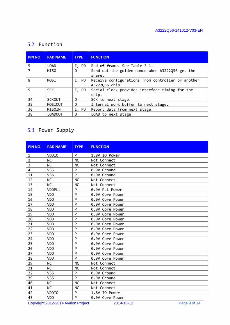
5.2 Function
PIN NO.
PAD NAME
TYPE
FUNCTION
5 LOAD I, PD End of frame. See Table 3-1. 7 MISO O Send out the golden nonce when A3222Q56 get the
share. 8 MOSI I, PD Receive configurations from controller or another
A3222Q56 chip. 9 SCK I, PD Serial clock provides interface timing for the
chip. 34 SCKOUT O SCK to next stage. 35 MOSIOUT O Internal work buffer to next stage. 36 MISOIN I, PD Report data from next stage. 38 LOADOUT O LOAD to next stage.
5.3 Power Supply
PIN NO.
PAD NAME
TYPE
FUNCTION
1 VDDIO P 1.8V IO Power 2 NC NC Not Connect 3 NC NC Not Connect 4 VSS P 0.9V Ground 11 VSS P 0.9V Ground 12 NC NC Not Connect 13 NC NC Not Connect 14 VDDPLL P 0.9V PLL Power 15 VDD P 0.9V Core Power 16 VDD P 0.9V Core Power 17 VDD P 0.9V Core Power 18 VDD P 0.9V Core Power 19 VDD P 0.9V Core Power 20 VDD P 0.9V Core Power 21 VDD P 0.9V Core Power 22 VDD P 0.9V Core Power 23 VDD P 0.9V Core Power 24 VDD P 0.9V Core Power 25 VDD P 0.9V Core Power 26 VDD P 0.9V Core Power 27 VDD P 0.9V Core Power 28 VDD P 0.9V Core Power 29 NC NC Not Connect 31 NC NC Not Connect 32 VSS P 0.9V Ground 39 VSS P 0.9V Ground 40 NC NC Not Connect 41 NC NC Not Connect 42 VDDIO P 1.8V IO Power 43 VDD P 0.9V Core Power

A3222Q56-141012-V03-EN
Copyright 2012-2014 Avalon Project 2014-10-12 Page 10 of 14
44 VDD P 0.9V Core Power 45 VDD P 0.9V Core Power 46 VDD P 0.9V Core Power 47 VDD P 0.9V Core Power 48 VDD P 0.9V Core Power 49 VDD P 0.9V Core Power 50 VDD P 0.9V Core Power 51 VDD P 0.9V Core Power 52 VDD P 0.9V Core Power 53 VDD P 0.9V Core Power 54 VDD P 0.9V Core Power 55 VDD P 0.9V Core Power 56 VDD P 0.9V Core Power
5.4 A3222Q56 Pin-Pad Map
A3222Q56
1 VDDIO
2 NC
3 NC
4 VSS
5 LOAD
6 RSTN
7 MISO
8 MOSI
9 SCK
10 XCLKIN
11 VSS
12 NC
13 NC
14 VDDPLL
42VDDIO
41NC
40NC
39VSS
38LOADOUT
37RSTNOUT
36MISOIN
35MOSIOUT
34SCKOUT
33XCLKOUT
32VSS
31NC
30TEST
29NC
28
VDD
27
VDD
26
VDD
25
VDD
24
VDD
23
VDD
22
VDD
21
VDD
20
VDD
19
VDD
18
VDD
17
VDD
16
VDD
15
VDD
43
VDD
44
VDD
45
VDD
46
VDD
47
VDD
48
VDD
49
VDD
50
VDD
51
VDD
52
VDD
53
VDD
54
VDD
55
VDD
56
VDD

A3222Q56-141012-V03-EN
Copyright 2012-2014 Avalon Project 2014-10-12 Page 11 of 14
6. ELECTRICAL CHARACTERISTICS
6.1 Recommended Operating Conditions The recommended operating conditions are the recommended values to assure normal
logic operation. As long as the device is used within the recommended operating
conditions, the electrical characteristics (DC and AC characteristics) described
below are assured.
PARAMETER.
SYMBOL
MIN
TYP
MAX
UNIT
Supply Core voltage
DVDD 0.75 0.75 0.9 V
Supply 1.0V analog voltage
VDDA_PLL 0.9 0.9 1.0 V
Supply I/O voltage
OVDD 1.8 1.8 1.8 V
Maximum input voltage
V i max
--
--
0.9
V
Operating Temperature
T OPR
-20
--
+85 ℃
Storage Temperature
T STOR
-40
--
+125 ℃
Operating Current
I OP
--
--
TBD
mA
Static Current I SUSP -- -- 20 mA
6.2 Oscillation
PARAMETER. CONDI TIONS
SYMBOL
MIN
TYP MAX
UNIT
Input clock frequency
--
Fclixin
--
25
--
MHz
Input clock period -- Tclkxin -- 40 -- Ns Clock duty cycle -- -- 45 50 55 % Input pad capacitance
--
--
--
3.398
--
Pf
Jitter -- -- -- -- 10 Ps Input HIGH leakage current
--
--
--
±10
uA
Input LOW leakage current
--
--
--
--
±10
uA

A3222Q56-141012-V03-EN
Copyright 2012-2014 Avalon Project 2014-10-12 Page 12 of 14
7. PACKAGE INFORMATION
7.1 A3222Q56 Package Specifications

A3222Q56-141012-V03-EN
Copyright 2012-2014 Avalon Project 2014-10-12 Page 13 of 14

A3222Q56-141012-V03-EN
Copyright 2012-2014 Avalon Project 2014-10-12 Page 14 of 14

A3222Q56-141012-V03-EN
Copyright 2012-2014 Avalon Project 2014-10-12 Page 15 of 14
8. REVISION HISTORY
Version No. Remarks Release Date 0.1 Initial version released for engineering review. 2014-06-27