Intracardiac acoustic radiation force impulse imaging: A ...
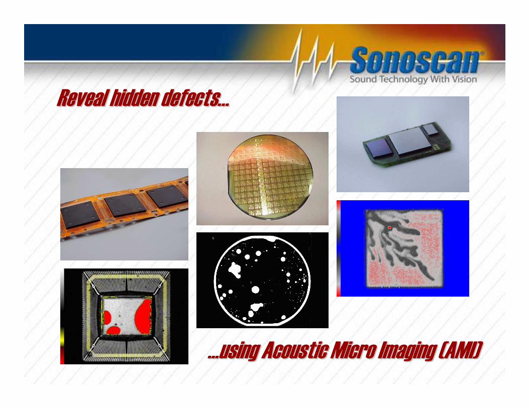
...using Acoustic Micro Imaging (AMI)...using Acoustic Micro Imaging (AMI)
Reveal hidden defectsReveal hidden defects……

What is Acoustic Micro Imaging?
Acoustic Micro Imaging (AMI) is a nondestructive
internal inspection technique that utilizes high frequency
ultrasound* in the range of 5 to 500 MHz.
*Ultrasound is defined as frequencies above 20 KHz
Why use Acoustic Micro Imaging?
1) determine interface bonding/adhesion
2) detect defects
3) characterize material properties
4) measure material properties
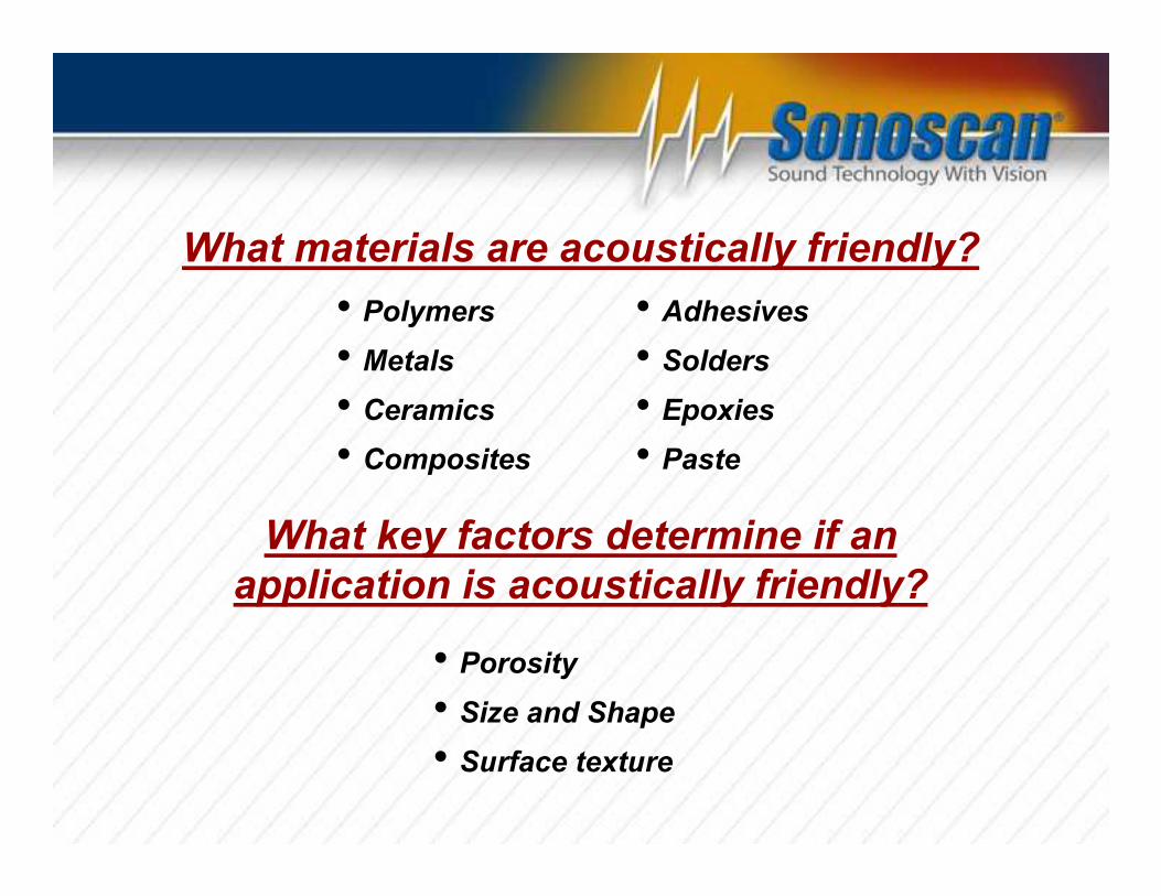
What materials are acoustically friendly?
• Polymers
• Metals
• Ceramics
• Composites
• Adhesives
• Solders
• Epoxies
• Paste
What key factors determine if an
application is acoustically friendly?
• Porosity
• Size and Shape
• Surface texture
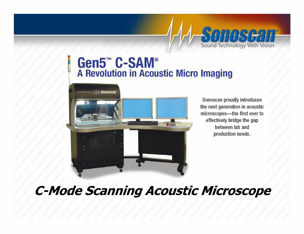
C-Mode Scanning Acoustic Microscope
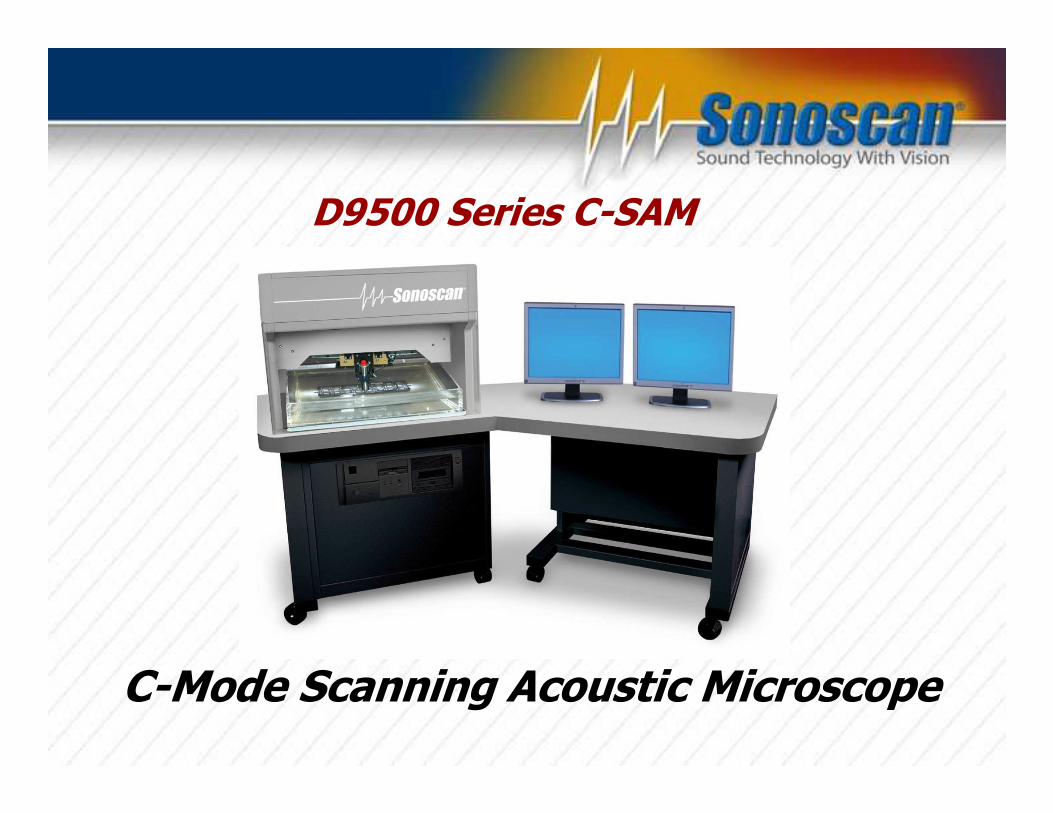
D9500 Series C-SAM
C-Mode Scanning Acoustic Microscope

C-Mode Scanning Acoustic Microscope
D24 Series C-SAM
Fast Automated C-Mode Tray Scanning System
FACTS2TM Series
Automated Bonded Wafer Inspection System
AW200 ™ Series C-SAM

Waterfall Transducer
Rotational Stage Fixture

Principles of Ultrasound
Within a given material ultrasound can be Reflected, Refracted, Transmitted, Scattered, Absorbed and/or
Blocked by changes relative to the surrounding material.

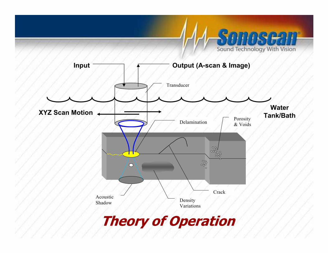
Porosity
& Voids
CrackAcoustic
Shadow
Delamination
Density
Variations
Transducer
Theory of Operation
Input Output (A-scan & Image)
XYZ Scan MotionWater
Tank/Bath
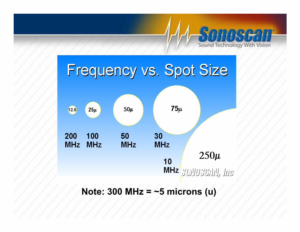
Note: 300 MHz = ~5 microns (u)
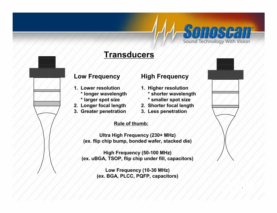
High FrequencyLow Frequency
Rule of thumb:
Ultra High Frequency (230+ MHz)
(ex. flip chip bump, bonded wafer, stacked die)
High Frequency (50-100 MHz)
(ex. uBGA, TSOP, flip chip under fill, capacitors)
Low Frequency (10-30 MHz)
(ex. BGA, PLCC, PQFP, capacitors)
1. Higher resolution
* shorter wavelength
* smaller spot size
2. Shorter focal length
3. Less penetration
1. Lower resolution
* longer wavelength
* larger spot size
2. Longer focal length
3. Greater penetration
Transducers

1
Si MetallizationSi MetallizationSi MetallizationSi Metallization
10 MHz10 MHz10 MHz10 MHz 100 MHz100 MHz100 MHz100 MHz 1 GHz1 GHz1 GHz1 GHz
Flip ChipsFlip ChipsFlip ChipsFlip Chips
Wafer BondingWafer BondingWafer BondingWafer Bonding
BGAsBGAsBGAsBGAs
Thick Film AdhesionThick Film AdhesionThick Film AdhesionThick Film Adhesion
Thin FilmsThin FilmsThin FilmsThin Films
Plastic ICsPlastic ICsPlastic ICsPlastic ICs
CSPCSPCSPCSP
Porosity & cracks in MetalsPorosity & cracks in MetalsPorosity & cracks in MetalsPorosity & cracks in Metals
CeramicsCeramicsCeramicsCeramics
Medical UltrasoundMedical UltrasoundMedical UltrasoundMedical Ultrasound
Hermetic Seal IntegrityHermetic Seal IntegrityHermetic Seal IntegrityHermetic Seal Integrity
Frequency vs. Applications


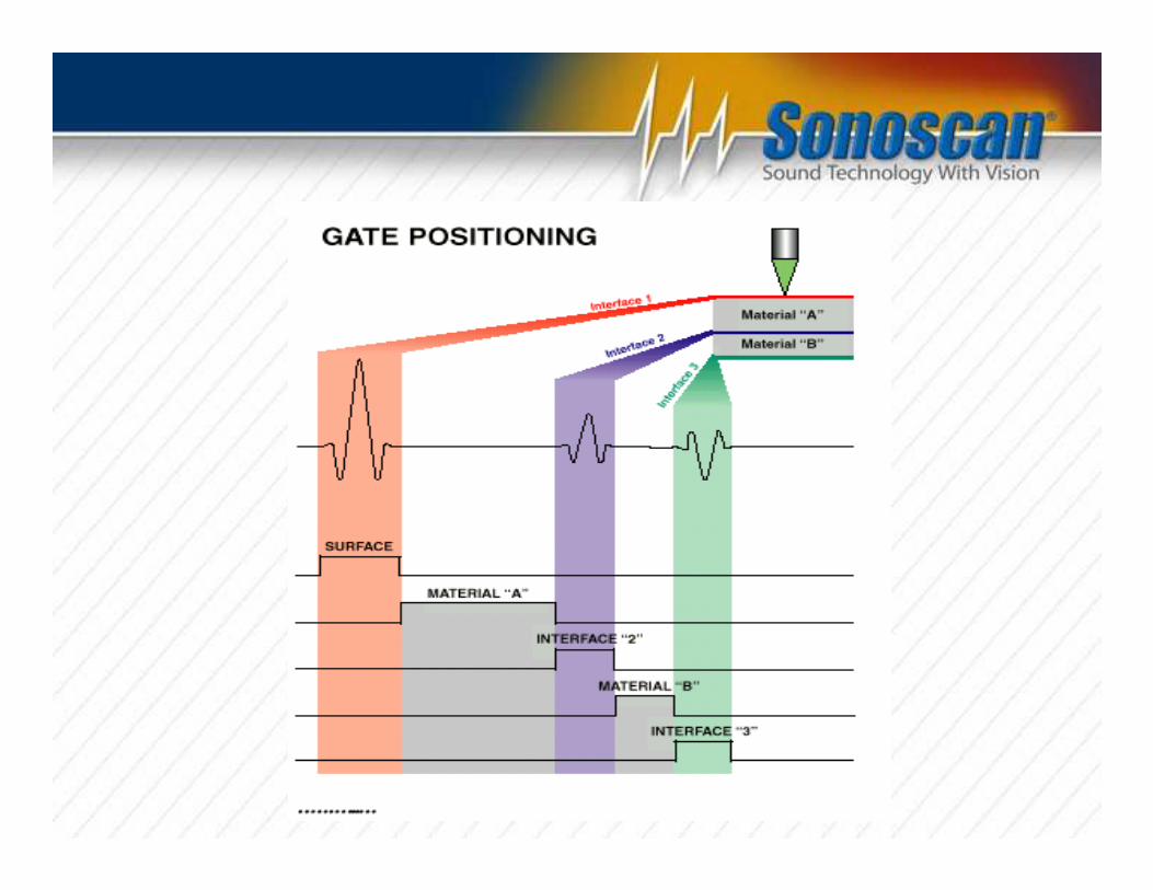
•The A-scan displays the mechanical signature (waveform) that corresponds to the position of the transducer over the sample.
•The A-scan is based on the acoustic impedance, thickness and velocity of the respective material(s).
•The A-scan includes time, amplitude and polarity (phase) information
A-scan Waveform Display

•Acoustic Impedance (Z) - is the product of a materials density times its ultrasonic velocity
Z = r V
•In practical terms - Acoustic Impedance is a materials characteristic property that
determines the amount of reflected and transmitted energy that occurs when an
ultrasonic wave encounters a boundary or interface between two materials.

Acoustic Impedance
Determines Echo
Polarity & Amplitude
R / I = (Z2 - Z1) / (Z2 + Z1)
Incident (I) Reflected (R)
Z1
Z2
CASE 1 Z2 > Z1
CASE 2 Z2 < Z1
CASE 3 Z2 = Z1
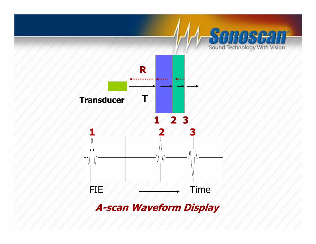
A-scan Waveform Display
Transducer T
R
21 3
21 3
TimeFIE

A-scan Amplitude, Polarity & Color Maps
Large Positive
Positive
No Signal
Negative
Large Negative
SymmetricAsymmetric


A-SCAN SURFACE SCAN C-SCAN
MULTI-SCAN
Q-BAM™ ZIP-SLICE & 3V™
BULK-SCAN THRU-SCAN
VRM ™ (Virtual Rescan Mode) with FDI & ASF
Modules
Imaging Modes

1 - Die Surface/Mold Compound (Interface Scan)
2 - Die Attach (Interface Scan)
3 & 7 - Lead Frame/Mold Compound (Interface Scan)
4 - Plastic Encapsulate
Void & Filler Distribution (Bulk Scan)
Material Characterization (Interface Scan)
5 -Die Pad/Molding Compound (Interface Scan)
6 - Surface Image (Surface Scan)
Plastic
Integrated
Circuit (PIC)
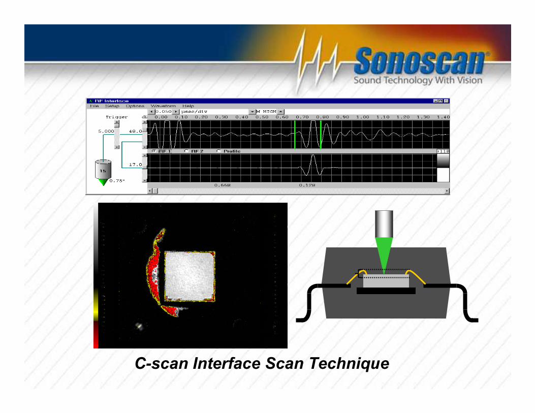
C-scan Interface Scan Technique
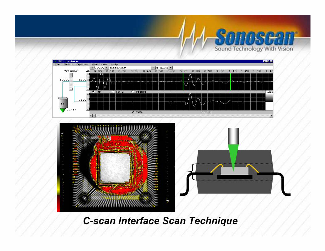
C-scan Interface Scan Technique

C-scan Bulk Scan Technique

Plastic Integrated Circuit (PIC) “Popcorn Crack”
ZIP-SLICE
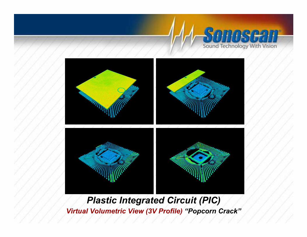
Plastic Integrated Circuit (PIC)Virtual Volumetric View (3V Profile) “Popcorn Crack”

1 - Surface Image (Surface Scan)
2 - Die Crack (Bulk Scan)
3 - Solder Bridging (Interface Scan)
4 - Chip to Underfill (Interface Scan)
5 - Underfill Voids (Interface Scan, Bulk Scan)
6 - Bump to Substrate (Interface Scan)
7 - Bump Integrity (Interface Scan, Bulk Scan)
Flip Chip/C4(Controlled Collapsed
Chip Connection)
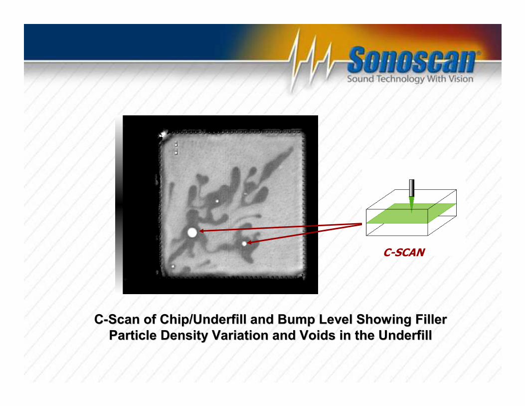
CC--Scan of Chip/Underfill and Bump Level Showing Filler Scan of Chip/Underfill and Bump Level Showing Filler
Particle Density Variation and Voids in the UnderfillParticle Density Variation and Voids in the Underfill
C-SCAN

CSP Flip Chip - Underfill
CC--scan Imagescan Image
Void/disbond Void/disbond ––
focused and gated at focused and gated at
the chip to underfill the chip to underfill
(upper) level (upper) level
CC--scan Imagescan Image
Void/disbond Void/disbond –– focused focused
and gated at the and gated at the
underfill to substrate underfill to substrate
(lower) level (lower) level
MULTI-SCAN

C4 Flip-chip Solder Bump Inspection
230 MHz C230 MHz C--scan Image scan Image
Voids/disbonds Voids/disbonds –– focused focused
and gated within the and gated within the
solder ballssolder balls
180 MHz C180 MHz C--scan Imagescan Image
Voids/disbonds Voids/disbonds –– focused focused
and gated within the and gated within the
solder ballssolder balls
C-SCAN
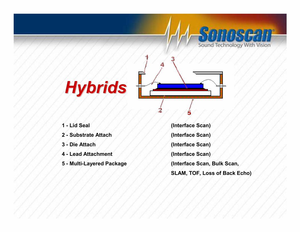
1 - Lid Seal (Interface Scan)
2 - Substrate Attach (Interface Scan)
3 - Die Attach (Interface Scan)
4 - Lead Attachment (Interface Scan)
5 - Multi-Layered Package (Interface Scan, Bulk Scan,
SLAM, TOF, Loss of Back Echo)
HybridsHybrids
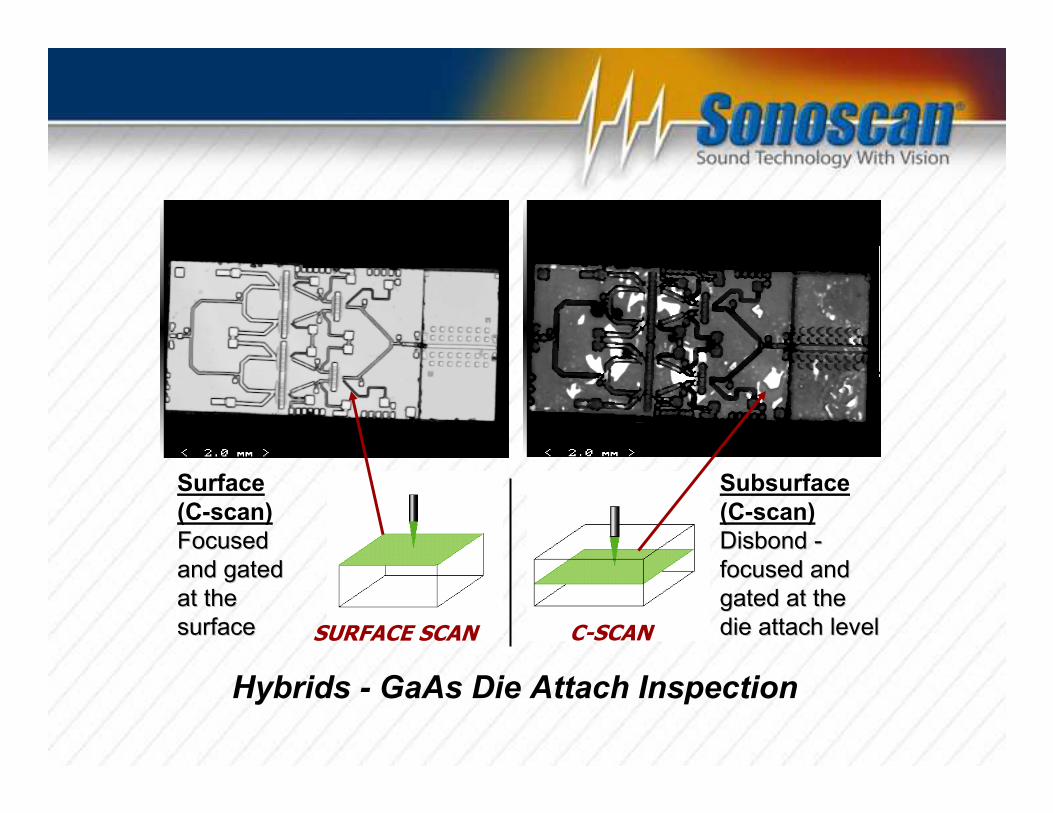
Hybrids - GaAs Die Attach Inspection
SURFACE SCAN C-SCAN
Surface
(C-scan)
Focused Focused
and gated and gated
at the at the
surfacesurface
Subsurface
(C-scan)
Disbond Disbond --
focused and focused and
gated at the gated at the
die attach leveldie attach level
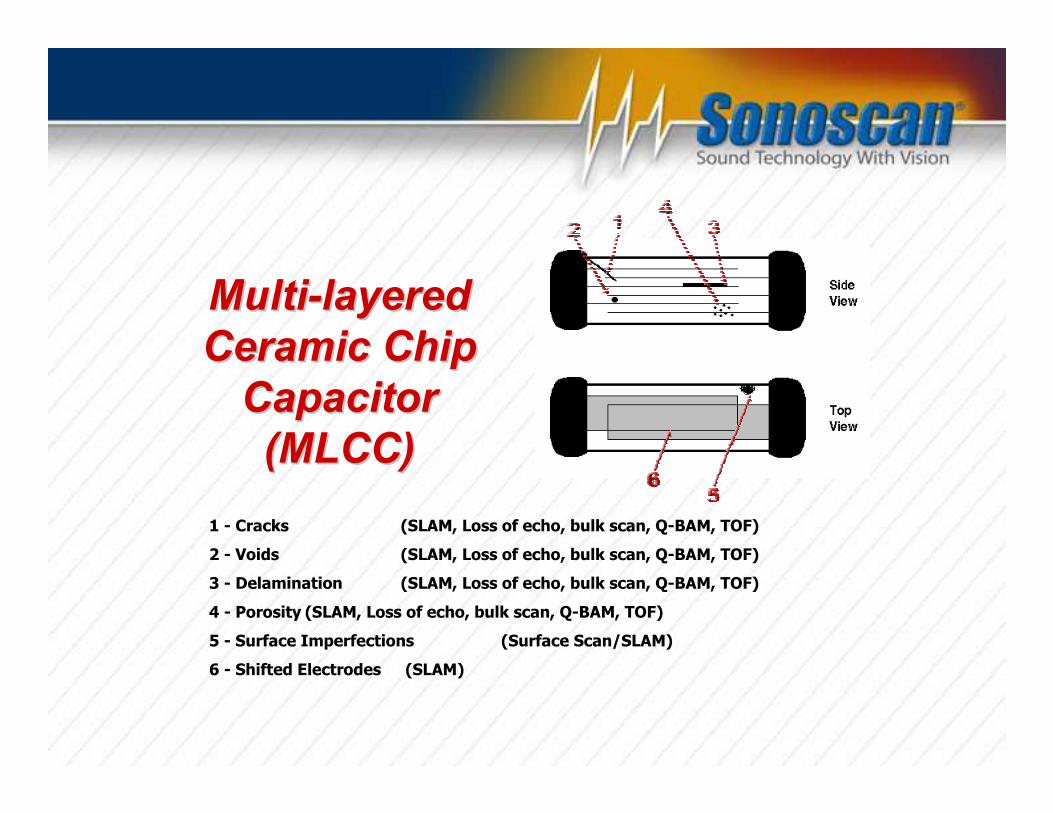
1 - Cracks (SLAM, Loss of echo, bulk scan, Q-BAM, TOF)
2 - Voids (SLAM, Loss of echo, bulk scan, Q-BAM, TOF)
3 - Delamination (SLAM, Loss of echo, bulk scan, Q-BAM, TOF)
4 - Porosity (SLAM, Loss of echo, bulk scan, Q-BAM, TOF)
5 - Surface Imperfections (Surface Scan/SLAM)
6 - Shifted Electrodes (SLAM)
MultiMulti--layered layered
Ceramic Chip Ceramic Chip
Capacitor Capacitor
(MLCC)(MLCC)

MultiMulti--layered Ceramic Chip Capacitor (MLCCC)layered Ceramic Chip Capacitor (MLCCC)
Q-BAM
Q-BAM (focused
B-scan image)
Disbond (left sample) Disbond (left sample)
-- focusedfocused and gated and gated
within the bulk ceramicwithin the bulk ceramicC-SCAN
C-scan image
Disbond (left sample) Disbond (left sample)
-- focused and gated focused and gated
within the bulk within the bulk
ceramicceramic
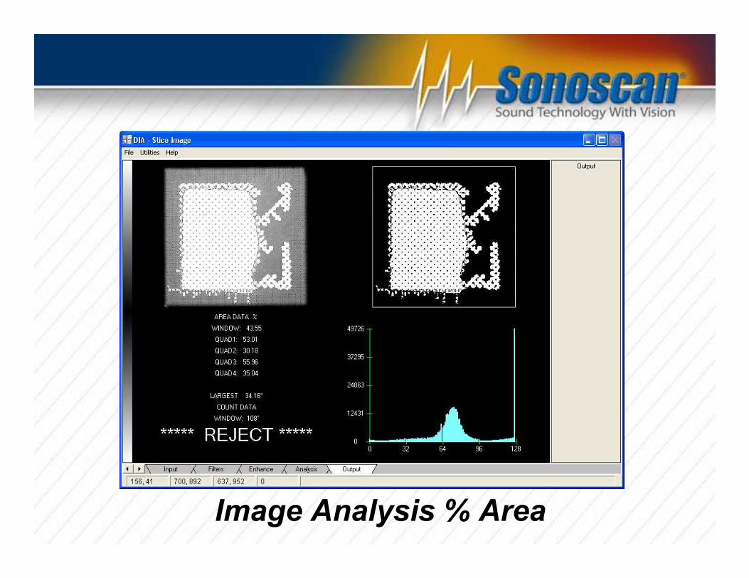
Image Analysis % Area
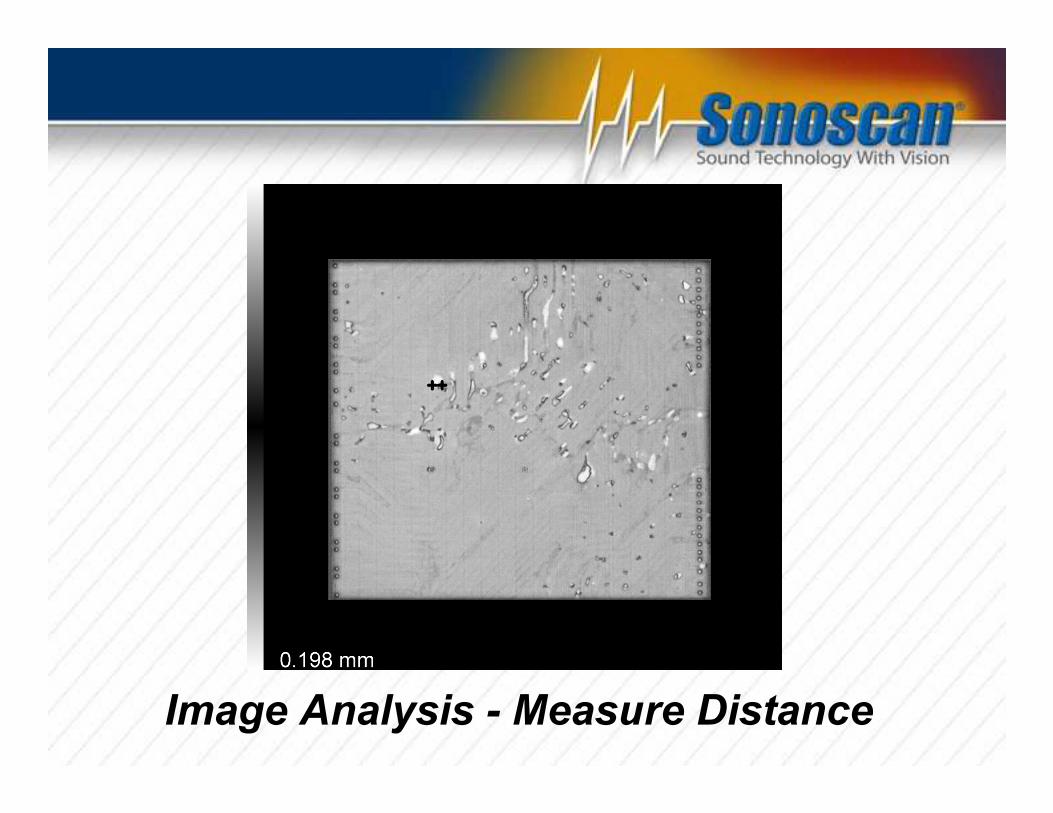
Image Analysis - Measure Distance
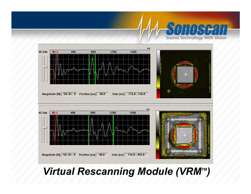
Virtual Rescanning Module (VRMTM)
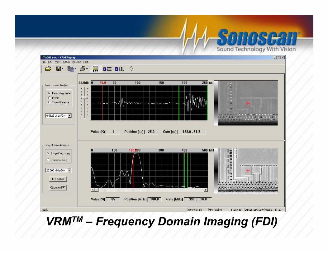
VRMTM – Frequency Domain Imaging (FDI)

141 MHz
175 MHz
167 MHz
195 MHz 226 MHz
Original Reconstruction
VRMTM – Frequency Domain Imaging (FDI)
VRMTM Acoustic Surface FlatnessASF Module
• A major new “tool” for Failure Analysis Labs• For a modest additional cost and training, and no
additional floor space, the customer gets the benefits and capability of an additional new “tool”.
• Compliments current capability by providing the analyst a new means to determine what is wrong with a part.
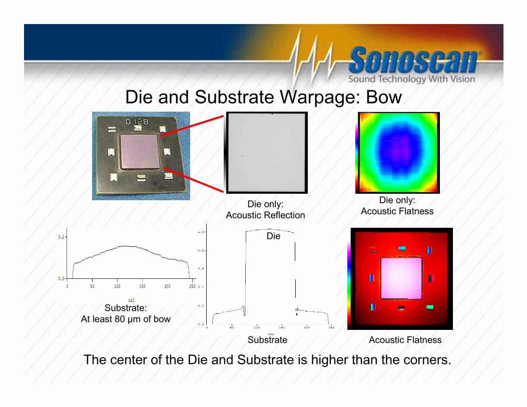
Die and Substrate Warpage: Bow
The center of the Die and Substrate is higher than the corners.
Die only:
Acoustic Reflection
Die only:
Acoustic Flatness
Die
Substrate
Substrate:
At least 80 µm of bow
Acoustic Flatness

PC Board: Warpage
If the PC Board isn’t a flat plane, then there can be solder problems.
Acoustic Reflection
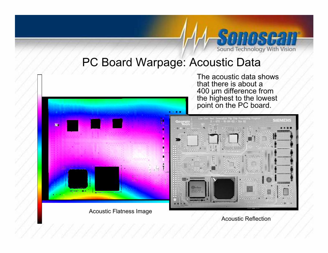
PC Board Warpage: Acoustic DataThe acoustic data shows that there is about a 400 µm difference from the highest to the lowest point on the PC board.
Acoustic Reflection
Acoustic Flatness Image

PC Board Warpage: Acoustic Data
mm
mm
The acoustic data shows that there is about a 400 µm difference from the highest to the lowest point on the PC board.

BGA Warpage on PC Board
Warpage (ccc) measured at ~35 µm.
Acoustic Reflection
Surface Internal Substrate
Acoustic FlatnessAcoustic Flatness
Projected Image

Substrate WarpageSubstrates
warpage can be either bow or warp.
Bow is shown here. The dark corners indicate that the center is bowed out.
Warp is like a potato chip shape (bent in two directions at the same time).
Thickness of the films on the substrate can also be measured. Acoustic Flatness
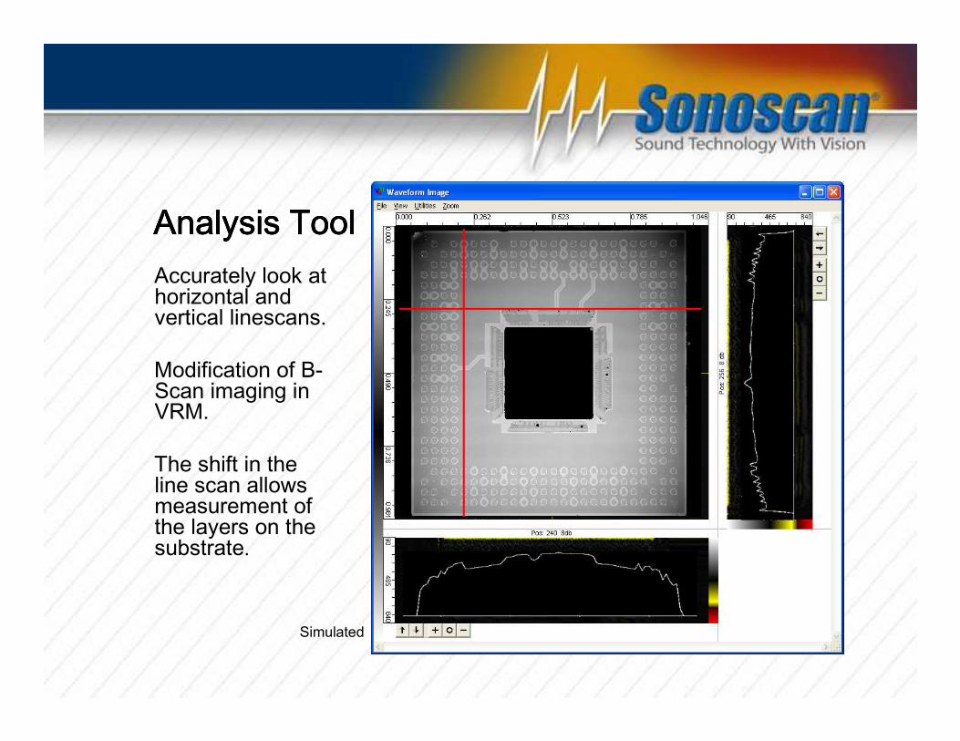
Analysis ToolAnalysis ToolAnalysis ToolAnalysis ToolAccurately look at horizontal and vertical linescans.
Modification of B-Scan imaging in VRM.
The shift in the line scan allows measurement of the layers on the substrate.
Simulated

![Acoustic Non-Line-of-Sight Imaging · Acoustic imaging techniques are also common in seismic applica-tions [4,26,40], for through-tissue imaging with ultra-sound [37], and for line-of-sight](https://static.fdocuments.us/doc/165x107/5f3a596d79197408c70ed0f8/acoustic-non-line-of-sight-acoustic-imaging-techniques-are-also-common-in-seismic.jpg)