USER MANUAL VAB-630cdn.viaembedded.com/products/docs/vab-630/User_Manual/UM...VAB -63 0 User Manual...
43
1.03-12312017-162000 USER MANUAL VAB-630 Cost effective single board computer with flexible I\O and rich connectivity
Transcript of USER MANUAL VAB-630cdn.viaembedded.com/products/docs/vab-630/User_Manual/UM...VAB -63 0 User Manual...

1.03-12312017-162000
USER MANUAL
VAB-630 Cost effective single board
computer with flexible I\O
and rich connectivity

Copyright
Copyright © 2016-2017 VIA Technologies Incorporated. All rights reserved.
No part of this document may be reproduced, transmitted, transcribed, stored in a retrieval system, or translated into any language,
in any form or by any means, electronic, mechanical, magnetic, optical, chemical, manual or otherwise without the prior written
permission of VIA Technologies, Incorporated.
Trademarks
All trademarks are the property of their respective holders.
Disclaimer
No license is granted, implied or otherwise, under any patent or patent rights of VIA Technologies. VIA Technologies makes no
warranties, implied or otherwise, in regard to this document and to the products described in this document. The information
provided in this document is believed to be accurate and reliable as of the publication date of this document. However, VIA
Technologies assumes no responsibility for the use or misuse of the information (including use or connection of extra
device/equipment/add-on card) in this document and for any patent infringements that may arise from the use of this document. The
information and product specifications within this document are subject to change at any time, without notice and without obligation
to notify any person of such change.
VIA Technologies, Inc. reserves the right the make changes to the products described in this manual at any time without prior notice.
Regulatory Compliance
FCC-A Radio Frequency Interference Statement
This equipment has been tested and found to comply with the limits for a class A digital device, pursuant to part 15 of the FCC rules.
These limits are designed to provide reasonable protection against harmful interference when the equipment is operated in a
commercial environment. This equipment generates, uses, and can radiate radio frequency energy and, if not installed and used in
accordance with the instruction manual, may cause harmful interference to radio communications. Operation of this equipment in a
residential area is likely to cause harmful interference, in which case the user will be required to correct the interference at his
personal expense.
Notice 1
The changes or modifications not expressly approved by the party responsible for compliance could void the user's authority to
operate the equipment.
Notice 2
Shielded interface cables and A.C. power cord, if any, must be used in order to comply with the emission limits.
Notice 3
The product described in this document is designed for general use, VIA Technologies assumes no responsibility for the conflicts or
damages arising from incompatibility of the product. Check compatibility issue with your local sales representatives before placing
an order.
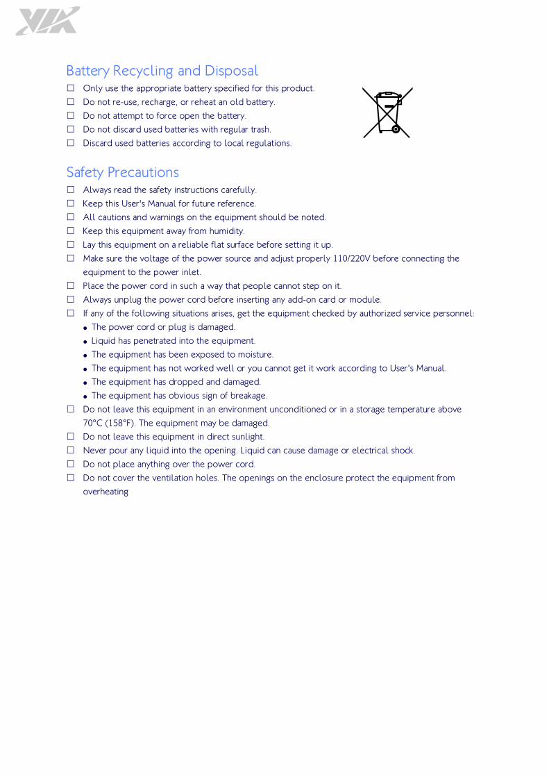
Battery Recycling and Disposal � Only use the appropriate battery specified for this product.
� Do not re-use, recharge, or reheat an old battery.
� Do not attempt to force open the battery.
� Do not discard used batteries with regular trash.
� Discard used batteries according to local regulations.
Safety Precautions � Always read the safety instructions carefully.
� Keep this User's Manual for future reference.
� All cautions and warnings on the equipment should be noted.
� Keep this equipment away from humidity.
� Lay this equipment on a reliable flat surface before setting it up.
� Make sure the voltage of the power source and adjust properly 110/220V before connecting the
equipment to the power inlet.
� Place the power cord in such a way that people cannot step on it.
� Always unplug the power cord before inserting any add-on card or module.
� If any of the following situations arises, get the equipment checked by authorized service personnel:
� The power cord or plug is damaged.
� Liquid has penetrated into the equipment.
� The equipment has been exposed to moisture.
� The equipment has not worked well or you cannot get it work according to User's Manual.
� The equipment has dropped and damaged.
� The equipment has obvious sign of breakage.
� Do not leave this equipment in an environment unconditioned or in a storage temperature above
70°C (158°F). The equipment may be damaged.
� Do not leave this equipment in direct sunlight.
� Never pour any liquid into the opening. Liquid can cause damage or electrical shock.
� Do not place anything over the power cord.
� Do not cover the ventilation holes. The openings on the enclosure protect the equipment from
overheating

VAB-630 User Manual
iv
Box Contents
VAB-630
� 1 x VAB-630 mainboard (with 1.0GHz VIA Cortex-A9 dual-core SoC)
� 1 x RTC battery
Ordering Information Part Number Description
10GHL126000A0 SBC with 1.0GHz VIA Cortex-A9 SoC, 4GB eMMC, 1GB DDR3 SDRAM
2 x USB 2.0, Micro USB 2.0 OTG, HDMI, COM, DIO, 10/100Mbps
Ethernet, Micro SD card slot, and 12V DC-in.
Optional Accessories
Wireless Accessories
Part Number Description
EMIO-2550-01A1 3.75G HSPA/UMTS mobile broadband full size miniPCIe module
EMIO-5531-00A1 VAB-820-W IEEE 802.11b/g/n USB Wi-Fi & Bluetooth module with
assembly kit
EMIO-2531-00A1 VAB-820-W-M IEEE 802.11b/g/n miniPCIe Wi-Fi & Bluetooth module
with assembly kit and antenna
Display Accessories
Part Number Description
STK-10630-00A0 10.1” LVDS LCD Touch panel (1280x800) with LVDS and Touch Cable
99G63-02033A 12V 36W adapter power adapter (power adapter plug not included)
VAB-630 User Manual
v
Table of Contents 1. Product Overview ........................................................................................................................ 1
1.1. Key Features ........................................................................................................................................................ 1
1.2. Product Specifications ...................................................................................................................................... 2
1.3. Layout Diagram .................................................................................................................................................. 4
1.4. Product Dimensions .......................................................................................................................................... 5
1.5. Height Distribution ............................................................................................................................................ 6
2. I/O Interface ................................................................................................................................... 7
2.1. External I/O Ports .............................................................................................................................................. 7
2.1.1. Micro SD Card Slot .................................................................................................................................... 8
2.1.2. 10/100Mbps Ethernet Port ....................................................................................................................... 8
2.1.3. USB 2.0 Port ................................................................................................................................................. 9
2.1.4. Audio Jacks ............................................................................................................................................... 10
2.1.5. Micro USB 2.0 OTG Port........................................................................................................................ 10
2.1.6. DIO Port .................................................................................................................................................... 11
2.1.7. Power LED ................................................................................................................................................ 11
2.1.8. Power Button ............................................................................................................................................ 12
2.1.9. DC-in Jack ................................................................................................................................................. 12
2.1.10. COM Port .................................................................................................................................................. 13
2.1.11. HDMI® Port ............................................................................................................................................... 13
2.2. Onboard Connectors ..................................................................................................................................... 14
2.2.1. SIM Card Slot ........................................................................................................................................... 14
2.2.2. MiniPCIe Slot ............................................................................................................................................ 15
2.2.3. I2C Touch Connector .............................................................................................................................. 16
2.2.4. LVDS Panel Connector ........................................................................................................................... 17
2.2.5. Battery Connector ................................................................................................................................... 18
2.2.6. Reset Connector ...................................................................................................................................... 18
2.2.7. RTC Battery Connector........................................................................................................................... 19
2.2.8. UART Connector ..................................................................................................................................... 19
2.2.9. USB 2.0 Connector .................................................................................................................................. 20
3. Hardware Installation ................................................................................................................ 21
3.1. Installing into a Chassis ................................................................................................................................. 21
3.1.1. Suggested minimum chassis dimensions ........................................................................................... 21
3.1.2. Suggested minimum chassis height ..................................................................................................... 21
3.1.3. Suggested keepout areas ....................................................................................................................... 22
4. Software and Technical Supports ........................................................................................... 23
4.1. Android Support............................................................................................................................................. 23
4.2. Technical Supports and Assistance ............................................................................................................ 23
Appendix A. Installing Wireless Accessories .............................................................................. 24
A.1. Installing the EMIO-2550 miniPCIe mobile broadband module ............................................................ 24
A.2. Installing the EMIO-2531 miniPCIe Wi-Fi & Bluetooth module .............................................................. 27
A.3. Installing EMIO-5531 USB Wi-Fi module ..................................................................................................... 29
Appendix B. Installing LVDS Panel Display .................................................................................. 31
B.1. Connecting the LVDS Panel Display to the VAB-630 board .................................................................... 31

VAB-630 User Manual
vi
Appendix C. Connector Vendor Lists ............................................................................................ 33
C.1. VAB-630 Mainboard .......................................................................................................................................... 33

VAB-630 User Manual
vii
List of Figures Figure 1: Layout diagram of the VAB-630 (top view) ..................................................................................................4
Figure 2: Layout diagram of the VAB-630 (bottom view) ...........................................................................................4
Figure 3: Mounting holes and dimensions of the VAB-630 (top view) ...................................................................5
Figure 4: External I/O port dimensions of the VAB-630 (front panel) ....................................................................5
Figure 5: External I/O port dimensions of the VAB-630 (back panel) .....................................................................5
Figure 6: Height distribution of the VAB-630 (top view) ............................................................................................6
Figure 7: Height distribution of the VAB-630 (bottom view) ....................................................................................6
Figure 8: Front panel I/O ....................................................................................................................................................7
Figure 9: Back panel I/O .....................................................................................................................................................7
Figure 10: Micro SD card slot diagram ............................................................................................................................8
Figure 11: 10/100Mbps Ethernet port diagram .............................................................................................................8
Figure 12: USB 2.0 port diagram .......................................................................................................................................9
Figure 13: Audio jack diagram ........................................................................................................................................ 10
Figure 14: Micro USB 2.0 OTG port diagram .............................................................................................................. 10
Figure 15: DIO port diagram........................................................................................................................................... 11
Figure 16: Power LED diagram ....................................................................................................................................... 11
Figure 17: Power button diagram .................................................................................................................................. 12
Figure 18: DC-in jack specification diagram ................................................................................................................ 12
Figure 19: DC-in jack diagram ........................................................................................................................................ 12
Figure 20: COM port diagram ........................................................................................................................................ 13
Figure 21: HDMI® port diagram ..................................................................................................................................... 13
Figure 22: SIM card slot diagram ................................................................................................................................... 14
Figure 23: MiniPCIe slot diagram ................................................................................................................................... 15
Figure 24: I2C touch connector diagram ...................................................................................................................... 16
Figure 25: LVDS panel connector diagram.................................................................................................................. 17
Figure 26: Battery connector diagram ............................................................................................................................ 18
Figure 27: Reset connector diagram ............................................................................................................................. 18
Figure 28: RTC battery connector diagram .................................................................................................................. 19
Figure 29: UART connector diagram ............................................................................................................................. 19
Figure 30: USB 2.0 connector diagram ......................................................................................................................... 20
Figure 31: Suggested minimum chassis dimensions .................................................................................................. 21
Figure 32: Suggested minimum internal ceiling height ............................................................................................ 21
Figure 33: Suggested keepout top areas...................................................................................................................... 22
Figure 34: Suggested keepout bottom areas .............................................................................................................. 22
Figure 35: Installing SIM Card......................................................................................................................................... 24
Figure 36: Inserting the EMIO-2550 module ............................................................................................................... 25
Figure 37: Securing the EMIO-2550 module .............................................................................................................. 25
Figure 38: Connecting the antenna cable and antenna ............................................................................................ 26
Figure 39: Connecting the antenna (to the micro-RF connector) .......................................................................... 26
Figure 40: Inserting the EMIO-2531 module ............................................................................................................... 27
Figure 41: Securing the EMIO-2531 module .............................................................................................................. 27
Figure 42: Connecting the Wi-Fi antenna cable and antenna ................................................................................. 28
Figure 43: Connecting the antenna cable to the micro-RF connector .................................................................. 28
Figure 44: Installing and securing EMIO-5531 module ............................................................................................ 29
Figure 45: Connecting USB Wi-Fi cable ....................................................................................................................... 29
Figure 46: Connecting the antenna cable and antenna ............................................................................................ 30
VAB-630 User Manual
viii
Figure 47: Connecting the antenna cable to the micro-RF connector .................................................................. 30
Figure 48: Connecting the touch screen cable to the touch controller module ............................................... 31
Figure 49: Connecting the USB touch cable ............................................................................................................... 31
Figure 50: Connecting the flex flat cable .................................................................................................................... 32

VAB-630 User Manual
ix
List of Tables
Table 1: Micro SD card slot pinouts ..............................................................................................................................8
Table 2: 10/100Mpbs Ethernet port pinouts ................................................................................................................8
Table 3: 10/100Mbps Ethernet port LED color definition .........................................................................................9
Table 4: USB 2.0 port pinouts ..........................................................................................................................................9
Table 5: Audio jack receptacle description .............................................................................................................. 10
Table 6: Micro USB 2.0 OTG port pinouts ................................................................................................................ 10
Table 7: DIO port pinouts ............................................................................................................................................. 11
Table 8: Power button behavior description ............................................................................................................ 12
Table 9: DC-in jack specification .................................................................................................................................. 12
Table 10: DC-in jack pinouts ........................................................................................................................................... 12
Table 11: COM port pinouts ........................................................................................................................................... 13
Table 12: HDMI® port pinouts ........................................................................................................................................ 13
Table 13 SIM card slot pinouts ...................................................................................................................................... 14
Table 14: MiniPCIe slot pinouts ...................................................................................................................................... 15
Table 15: I2C touch connector pinouts ......................................................................................................................... 16
Table 16: LVDS panel connector pinouts..................................................................................................................... 17
Table 17: Battery connector pinouts ............................................................................................................................. 18
Table 18: Reset connector pinouts ................................................................................................................................ 18
Table 19: RTC battery connector pinouts ..................................................................................................................... 19
Table 20: UART connector pinouts ................................................................................................................................ 19
Table 21: USB 2.0 connector pinouts ............................................................................................................................ 20
Table 22: VAB-630 connector vendor lists .................................................................................................................. 33
VAB-630 User Manual
1
1. Product Overview Based with a compacted 3.5 inch SBC and measuring at 14.6cm x 10.2cm, the VIA VAB-630 is a highly
integrated based ARM board. It’s powered by 1.0GHz VIA Cortex-A9 dual-core processor. The VIA VAB-
630 combines two independent, integrated GPUs for 3D/2D graphics acceleration, in addition it offers
support for MPEG-2 and H.264 video decoding up to 1080p.
The VIA VAB-630 mainboard has been optimized to support 3G, Wi-Fi and Bluetooth function with its rich
I\O, optional accessories includes a 10.1” touch panel that brings application like HMI and digital signage
product more easily to fit-in application. Users will find it easier for them to create and enhance their
apps with VIA VAB-630 mainboard.
The VIA VAB-630 provides an impressive selection of rear I/O in a compact form factor including HDMI®
port, two USB 2.0 ports, DC-in jack and 10/100Mbps Ethernet port. Customers can take advantage of VIA’s
industry leading hardware and software support to create customized designs with a quick time to market.
The VIA VAB-630 is also available with board support packages (BSP) for Android operating systems.
1.1. Key Features • Powered by 1.0GHz VIA Cortex-A9 dual-core SoC
• Supports independent, integrated graphic processing (GPU) for 3D/2D and graphic acceleration
• Supports HDMI port, 10/100Mbps Ethernet port and Audio jack
• Supports one single-channel 18/24 bit LVDS connector
• Supports both 3G and Wi-Fi + Bluetooth module connection
• Supports 10 GPIO with 3.3V power
• Supports power by DC-in or battery mode
• Android 5.0 operating system
• Fanless and ultra-low power consumption
• 4GB onboard eMMC Flash memory
• Flawless HD video performance up to 1080p
• Supports Micro USB 2.0 OTG.
• Android solution pack available
• Optional 12V (default) or 5V power input

VAB-630 User Manual
2
1.2. Product Specifications
Processor
o 1.0GHz VIA Cortex-A9 dual-core SoC
System Memory
o 1GB DDR3 SDRAM onboard
Storage
o 4GB eMMC Flash memory
Boot Loader
o 512KB SPI Flash ROM
Graphics
o Mali-400 SP GPU
• 2-integrated, independent 3D/2D graphics processing units
• Graphic engine supporting OpenGL® ES 2.0 hardware acceleration
• Conditional supports MPEG-2 and H.264 video decoding up to 1080p
LAN
o ASIC AX88772CLF
Audio
o VIA VT1603A I2S Audio Codec
HDMI
o Integrated HDMI 1.4 Transmitter
Onboard I/O
o 1 x USB 2.0 connector
o 1 x Single-channel 18/24 bit LVDS panel connector
o 1 x I2C touch connector
o 1 x UART (console port connector)
o 1 x RTC battery connector
o 1 x Reset connector
o 1 x miniPCle slot
o 1 x SIM card slot
o 1 x Battery connector
Front Panel I/O
o 1 x Micro SD card slot
o 1 x Micro USB 2.0 OTG port
o 1 x Power button
o 1 x DIO port supports 10 GPIO with 3.3V power
o 1 x Power LED
o 2 x Audio jacks (Line-out and Mic-in)

VAB-630 User Manual
3
Back Panel I/O
o 1 x HDMI port
o 2 x USB 2.0 ports
o 1 x COM port for RS-232 (TX/RX)
o 1 x 10/100Mbps Ethernet port
o 1 x DC in-jack
Power Supply
o 12V DC-in (5V DC-in optional)
Operating Temperature
o 0°C ~ 60°C
Operating Humidity
o 0% ~ 95% @ 40°C (non-condensing)
Operating System
o Android 5.0
Form Factor
o 3.5 inch SBC
o 14.6cm x 10.2cm (146mm x 102mm)
Compliance
o CE, FCC
Notes:
1. As the operating temperature provided in the specifications is a result of the test performed in VIA’s
chamber, a number of variables can influence this result. Please note that the working temperature may vary
depending on the actual situation and environment. It is highly suggested to execute a solid testing program
and take all the variables into consideration when building the system. Please ensure that the system runs
well under the operating temperature in terms of application.
2. Please note that the lifespan of the onboard eMMC memory chip may vary depending on the amount of
access. More frequent and larger data access on eMMC memory makes its lifespan shorter. Therefore, it is
highly recommended to use a replaceable external storage (e.g., Micro SD card) for large data access.

VAB-630 User Manual
4
1.3. Layout Diagram
OPEN
LO
CK
VAB - 630
UART
miniPCIe
External I/O
SIM Card slot
USB 2.0
Reset
RTC battery connector
Battery connector
eMMC
1.0GHz VIA Cortex-A9
dual-core SoC
External I/O
DDR3 SDRAM
Figure 1: Layout diagram of the VAB-630 (top view)
LVDS
I C touch2
Figure 2: Layout diagram of the VAB-630 (bottom view)

VAB-630 User Manual
5
1.4. Product Dimensions
OPEN
LOCK
VAB - 630
146mm
3mm
O 3.5mm (hole)
102mm
70.5mm
7mm
9mm 3mm
Figure 3: Mounting holes and dimensions of the VAB-630 (top view)
101mm
119.5mm
132.5mm
28mm
86mm
45.5mm
1.4mm
19.5mm
Figure 4: External I/O port dimensions of the VAB-630 (front panel)
102mm
121mm
25mm
75.5mm
55mm
Figure 5: External I/O port dimensions of the VAB-630 (back panel)

VAB-630 User Manual
6
1.5. Height Distribution
OPEN
LOCK
V������
H���� � ��
������� ���� ������� ����������� ����������� �����
������� ����mm������� �����
H���� ����
������� ����
H���� � ��
Figure 6: Height distribution of the VAB-630 (top view)
�� !"#$ %&'((
Figure 7: Height distribution of the VAB-630 (bottom view)

VAB-630 User Manual
7
2. I/O Interface The VAB-630 has a selection of interfaces integrated into the board. It includes a selection of frequently
used ports as part of the external I/O coastline.
2.1. External I/O Ports
D)* P+,-. /011+2
P+,-. 34D
M56.+ 789 :;< *=>M56?52
352-?+01
M56.+ 8D @a.A BC+1
Figure 8: Front panel I/O
10/100Mbps Ethernet
COMDC-in USB 2.0
10/100Mbps Ethernet
COMDC-in USB 2.0HDMI
Figure 9: Back panel I/O

VAB-630 User Manual
8
2.1.1. Micro SD Card Slot The main board comes with a Micro SD card slot located on the front panel with support for a maximum
storage capacity of 32GB. The pinouts of the Micro SD card slot are shown below.
Figure 10: Micro SD card slot diagram
Pin Signal
1 SD0DATA2
2 SD0DATA3
3 SD0CMD
4 VCC33_SDO
5 SD0CLK
6 GND
7 SD0DATA0
8 SD0DATA1
9 SD0CD-
Table 1: Micro SD card slot pinouts
2.1.2. 10/100Mbps Ethernet Port The mainboard is equipped with a 10/100Mbps Ethernet port which uses an 8 Position 8 Contact (8P8C)
receptacle connector or commonly referred to as RJ-45. It is fully compliant with IEEE 802.3 (10BASE-T)
and 802.3u (100BASE-TX). The pinouts of the 10/100Mbps Ethernet port are shown below.
18
Figure 11: 10/100Mbps Ethernet port diagram
Pin Signal
1 TD+
2 TD-
3 RD+
4 REGOUT
5 REGOUT
6 RD-
7 GND
8 GND
Table 2: 10/100Mpbs Ethernet port pinouts

VAB-630 User Manual
9
The 10/100Mbps Ethernet port (RJ-45) is equipped with two LED indicators on the front side to show its
Active/ Link status and Speed status.
Link LED
(Left LED on RJ-45 port)
Active LED
(Right LED on RJ-45 port)
Link Off LED is off LED is off
Speed_10Mbit The Green LED is on Yellow Flash
Speed_100Mbit The Green LED is on Yellow Flash
Table 3: 10/100Mbps Ethernet port LED color definition
2.1.3. USB 2.0 Port The mainboard provides two USB 2.0 ports. Each USB ports gives complete Plug and Play and hot swap
capability for external devices. The USB interface complies with USB UHCI, Rev. 2.0. The pinouts of the
typical USB 2.0 port is shown below.
4 1
4 1
Figure 12: USB 2.0 port diagram
USB0 USB1
Pin Signal Pin Signal
1 VCC 1 VCC
2 USB data - 2 USB data -
3 USB data + 3 USB data +
4 GND 4 GND
Table 4: USB 2.0 port pinouts

VAB-630 User Manual
10
2.1.4. Audio Jacks The mainboard offers High Definition Audio through 3.5mm Tip Ring Sleeve (TRS) connector to enable
connections to Line-out and Mic-in. The Line-out jack is for connecting to external speakers or
headphones. The Mic-in is for connecting to a microphone.
LEFGIJKNOEQIEF
Figure 13: Audio jack diagram
Jack Description
Mic-in TRS jack, 3.5mm Ø 5P, 90 Degree, Female, shielded
Line-out TRS jack, 3.5mm Ø 5P, 90 Degree, Female, shielded
Table 5: Audio jack receptacle description
2.1.5. Micro USB 2.0 OTG Port The mainboard comes with a Micro USB 2.0 type B port located on the front panel which gives complete
Plug and Play and hot swap capability for external devices. The USB interface complies with USB UHCI,
Rev. 2.0 and it supports OTG function. The pinouts of the Micro USB 2.0 OTG port are shown below.
5 1
Figure 14: Micro USB 2.0 OTG port diagram
Pin Signal
1 USB_VBUS0
2 USB_HD0-
3 USB_HD0+
4 USBID0
5 GND
Table 6: Micro USB 2.0 OTG port pinouts

VAB-630 User Manual
11
2.1.6. DIO Port The mainboard comes with a female DIO port for digital I/O communication interface port. The DIO port
is using D-sub 15-pin connector. The pinouts of the DIO port are shown below.
5
10
15
1
6
11
Figure 15: DIO port diagram
Pin Signal
1 GPIO1
2 GPIO2
3 GPIO3
4 GPIO5
5 GPIO6
6 GPIO7
7 GPIO8
8 GND
9 NC
10 GPIO12
11 GPIO13
12 GPIO14
13 VO_33
14 VO_33
15 GND
Table 7: DIO port pinouts
2.1.7. Power LED The mainboard comes with a Power LED which is located on the front panel. It is green and indicates the
status of the system.
Figure 16: Power LED diagram

VAB-630 User Manual
12
2.1.8. Power Button The mainboard is equipped with a power button. The Power button can support four functions. The table
below will explain how the functions work.
Figure 17: Power button diagram
Power Button Behavior
Suspend/Resume System Quickly press the power button once to suspend. While in suspending
mode quickly press once to resume
Popup power control menu Occurs when the power button is pressed for longer than 3 seconds.
Power On When the system is forced to power off, press the power button to
power back on.
Reset mode Occurs when the power button is pressed for longer than 6 seconds.
Table 8: Power button behavior description
Note:
1. Suspend mode may be interrupted by the Android’s original behavior.
2.1.9. DC-in Jack The mainboard comes with a DC power input jack on the back I/O panel adjacent to the HDMI. The
power connector carriers +12V DC external power input. The specifications and pinout of power
connector are shown below.
O 6.0mm O 2.5mm
Figure 18: DC-in jack specification diagram
Physical Specification
Outer Diameter 6.0mm
Inner Diameter 2.5mm
Barrel Depth 8.2mm
Electrical Specification
Input Voltage +12V
Table 9: DC-in jack specification
12
Figure 19: DC-in jack diagram
Pin Signal
1 12VIN
2 GND
Table 10: DC-in jack pinouts

VAB-630 User Manual
13
2.1.10. COM Port The mainboard is equipped 9-pin COM port uses a male DE-9 connector. The COM port supports the
RS-232 standard. The pinouts of the COM port are shown below.
1 5
6 9
Figure 20: COM port diagram
Pin Signal
1 NC
2 IC_RXD1
3 IC_TXD1
4 NC
5 GND
6 NC
7 NC
8 NC
9 NC
Table 11: COM port pinouts
2.1.11. HDMI® Port The mainboard is equipped with an HDMI port on the back panel which uses a HDMI port Type A
receptacle connector to connect high definition video and digital audio using a single cable. The pinouts
of the HDMI port are shown below.
Figure 21: HDMI® port diagram
Pin Signal Pin Signal
1 HDMI2+ 2 GND
3 HDMI2- 4 HDMI1+
5 GND 6 HDMI1-
7 HDMI0+ 8 GND
9 HDMI0- 10 HDMICLK+
11 GND 12 HDMICLK-
13 HDMICEC 14 NC
15 HDMIDDCSCL 16 HDMIDDCSDA
17 GND 18 5V_HDMI
19 HDMIHPD
Table 12: HDMI® port pinouts
VAB-630 User Manual
14
2.2. Onboard Connectors
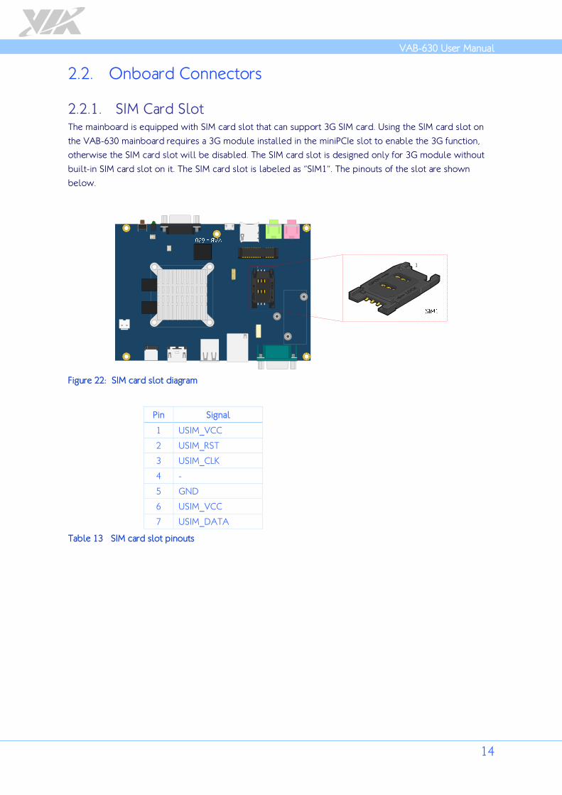
2.2.1. SIM Card Slot The mainboard is equipped with SIM card slot that can support 3G SIM card. Using the SIM card slot on
the VAB-630 mainboard requires a 3G module installed in the miniPCIe slot to enable the 3G function,
otherwise the SIM card slot will be disabled. The SIM card slot is designed only for 3G module without
built-in SIM card slot on it. The SIM card slot is labeled as “SIM1”. The pinouts of the slot are shown
below.
OPEN
LOCK
RSTUWXY
1
LOCK
OPEN
Z[\]
1
Figure 22: SIM card slot diagram
Pin Signal
1 USIM_VCC
2 USIM_RST
3 USIM_CLK
4 -
5 GND
6 USIM_VCC
7 USIM_DATA
Table 13 SIM card slot pinouts

VAB-630 User Manual
15
2.2.2. MiniPCIe Slot The mainboard is equipped with miniPCIe slot for wireless networking option such as WPAN/Wi-Fi/
WWAN. The miniPCIe slot is compatible with all PCIe 2.0 miniPCIe modules full-length. The pinouts of
the miniPCIe slot are shown below.
OPEN
LOCK
^_`bcde
1
fghgijgkl
1
Figure 23: MiniPCIe slot diagram
Pin Signal Pin Signal
1 NC 2 3.3V
3 NC 4 GND
5 NC 6 +1.5V
7 3.3V 8 USIM_VCC
9 GND 10 USIM_DATA
11 NC 12 USIM_CLK
13 NC 14 USIM_RST
15 GND 16 NC
17 NC 18 GND
19 NC 20 -W_DISABLE
21 GND 22 SUSGP1O2
23 NC 24 3.3V
25 NC 26 GND
27 GND 28 +1.5v
29 GND 30 12C4SCL
31 NC 32 12C4SDA
33 NC 34 GND
35 GND 36 USBDT2-
37 GND 38 USBDT2+
39 3.3V 40 GND
41 3.3V 42 NC
43 GND 44 NC
45 NC 46 NC
47 NC 48 +1.5V
49 NC 50 GND
51 NC 52 3.3V
Table 14: MiniPCIe slot pinouts

VAB-630 User Manual
16
2.2.3. I2C Touch Connector The mainboard is equipped with an I²C touch connector for connecting resistive touch panel. The I²C
touch connector is labeled as "JTOUCH1". The pinouts of the I2C touch connector are shown below.
mnopqrs
1
1
Figure 24: I2C touch connector diagram
Pin Signal
1 GPIO9
2 GPIO4
3 I2C1SDA
4 I2C1SCL
5 GND
6 VCC33
Table 15: I2C touch connector pinouts

VAB-630 User Manual
17
2.2.4. LVDS Panel Connector The mainboard has a LVDS panel connector on the bottom side which is used to connect the panel’s
LVDS cable to support the single-channel 18/24-bit display. Backlight controls are integrated into the
LVDS panel connector pinouts. The LVDS panel connector is labeled as “LVDS1”. The pinouts of the LVDS
panel connector are shown below.
1
tuvwx
1
Figure 25: LVDS panel connector diagram
Pin Signal Pin Signal
1 VLED+ 2 VLED+
3 VGH 4 CABC0
5 CABC1 6 VGL
7 UD 8 LR
9 VLED- 10 VLED-
11 GND 12 AVDD
13 SELB 14 NC
15 NC 16 GND
17 NC 18 NC
19 GND 20 LVDS_3+
21 LVDS_3- 22 GND
23 LVDS_CLK+ 24 LVDS_CLK-
25 GND 26 LVDS_2+
27 LVDS_2- 28 GND
29 LVDS_1+ 30 LVDS_1-
31 GND 32 LVDS_0+
33 LVDS_0- 34 GND
35 STBYB 36 NRST
37 NC 38 LCDVDD
39 LCDVDD 40 VCOM
Table 16: LVDS panel connector pinouts

VAB-630 User Manual
18
2.2.5. Battery Connector The mainboard is equipped with an onboard battery charger connector used for connecting the external
cable for charging a rechargeable battery; in addition it provides power to the board. A well packed 4.2V
battery with overcharge prevention and over discharge prevention/protection function embedded in
battery pack is required to be used with VAB-630.The battery connector is labeled as “J3”. The connector
pinouts are shown below.
OPEN
LOCK
yz{|}~�
1
��
1
Figure 26: Battery connector diagram
Pin Signal
1 VPACK+
2 GND
Table 17: Battery connector pinouts
2.2.6. Reset Connector The mainboard is equipped with an onboard reset button that allows the user to reboot or reset the
system forcibly without turning off the system power. A cable or switch must be applied for this to take
place. The pinouts of the reset connector are shown below.
OPEN
LOCK
�������1
����
1
Figure 27: Reset connector diagram
Pin Signal
1 GND
2 Reset
Table 18: Reset connector pinouts

VAB-630 User Manual
19
2.2.7. RTC Battery Connector The mainboard is equipped with is equipped with an onboard RTC battery connector which is used for
connecting the external cable battery that provides power to the 32.768KHz crystal oscillator for Real
Time Clock (RTC). The RTC battery connector is labeled as “J53”. The pinouts of the RTC battery
connector are shown below.
OPEN
LOCK
�������1
����
1
Figure 28: RTC battery connector diagram
Pin Signal
1 GND
2 V_RTC
Table 19: RTC battery connector pinouts
2.2.8. UART Connector The mainboard includes one UART connector which is used for debugging purposes. It is labeled as “J1”.
The UART connector pinouts are shown below.
OPEN
LOCK
�������
� 1
1
Figure 29: UART connector diagram
Pin Signal
1 UART0TXD
2 UART0RXD
3 SFCLK
4 GND
5 SFDO
6 SFDI
7 SFCS0-
8 VCC_SF
Table 20: UART connector pinouts

VAB-630 User Manual
20
2.2.9. USB 2.0 Connector The mainboard includes one USB 2.0 connector designed for connecting the USB Wi-Fi module (EMIO-
5531). The pinouts of the pin header are shown below.
OPEN
LOCK
¡¢£¤¥¦§
1
1
¨©ª«¬
Figure 30: USB 2.0 connector diagram
Pin Signal
1 NC
2 -
3 GND
4 USBT1+
5 USBT1-
6 5VUSB1
Table 21: USB 2.0 connector pinouts

VAB-630 User Manual
21
3. Hardware Installation
3.1. Installing into a Chassis The VAB-630 can be fitted into any chassis that has the mounting holes compatible with the standard SBC
mounting holes locations. Additionally, the chassis must meet the minimum height requirements for
specified areas of the mainboard.
3.1.1. Suggested minimum chassis dimensions The figure below shows the suggested minimum space requirements that a chassis should have in order to
work well with the VAB-630.
OPEN
LOCK
®¯°±²³
1.5mm
1.5mm
2mm2mm
Figure 31: Suggested minimum chassis dimensions
Each side of the mainboard should have a buffer zone from the internal wall of the chassis. The side of the
mainboard that accommodates the I/O coastline should have a buffer of 1.5mm; it’s comprised of a Mic-in,
Line-out, Micro USB 2.0 OTG, Micro SD card slot, DIO, Power LED and Power button. The side on the
opposite end of the I/O coastline should have a buffer of at least 1.5mm; it’s comprised of DC-in jack,
HDMI, USB 2.0, 10/100Mbps Ethernet and COM. The two sides adjacent to the I/O coastline should have
at least a buffer 2.0mm.
3.1.2. Suggested minimum chassis height The figure below shows the suggested minimum height requirements for the internal space of the chassis.
It is not necessary for the internal ceiling to be evenly flat. What is required is that the internal ceiling
height must be strictly observed for each section that is highlighted.
OPEN
LOCK
´µ¶·¸¹º
17mm
19mm
17mm
19mm
Figure 32: Suggested minimum internal ceiling height

VAB-630 User Manual
22
3.1.3. Suggested keepout areas The figure below shows the areas of the mainboard that is highly suggested to leave unobstructed. The
figures below are the top view and the bottom view.
OPEN
LOCK
»¼½¾¿ÀÁ
Figure 33: Suggested keepout top areas
Figure 34: Suggested keepout bottom areas

VAB-630 User Manual
23
4. Software and Technical Supports
4.1. Android Support The VAB-630 features a complete software evaluation image featuring Android 5.0 operating system.
4.2. Technical Supports and Assistance • For utilities downloads, latest documentation and new information about VAB-630, please visit
our website https://www.viatech.com/en/boards/3-5-inch-sbc/vab-630/
• For technical support and additional assistance, always contact your local sales representative or
board distributor, or go to https://www.viatech.com/en/support/driver-support-faq/technical-
support/ for technical support.
• For OEM clients and system integrators developing a product for long term production, other
code and resources may also be made available. Please visit our website at
https://www.viatech.com/en/ about/contact/ to submit a request.

VAB-630 User Manual
24
Appendix A. Installing Wireless Accessories This chapter provides you with information on how to install the EMIO modules and connect LVDS panel
display into the VAB-630 board. It is recommended to use a grounded wrist strap before handling
computer components. Electrostatic discharge (ESD) can damage some components.
A.1. Installing the EMIO-2550 miniPCIe mobile broadband
module
Step 1
Pull up the slot and place the SIM card inside the slot. Ensure the angled corner of the SIM card is placed
in the correct way before closing the slot.
Figure 35: Installing SIM Card
ÂÃÄÅÆÇÈ
LOCK
OPEN
ÉÊËÌÍÎÏÐ
1 2 3 4
VAB-630 User Manual
25
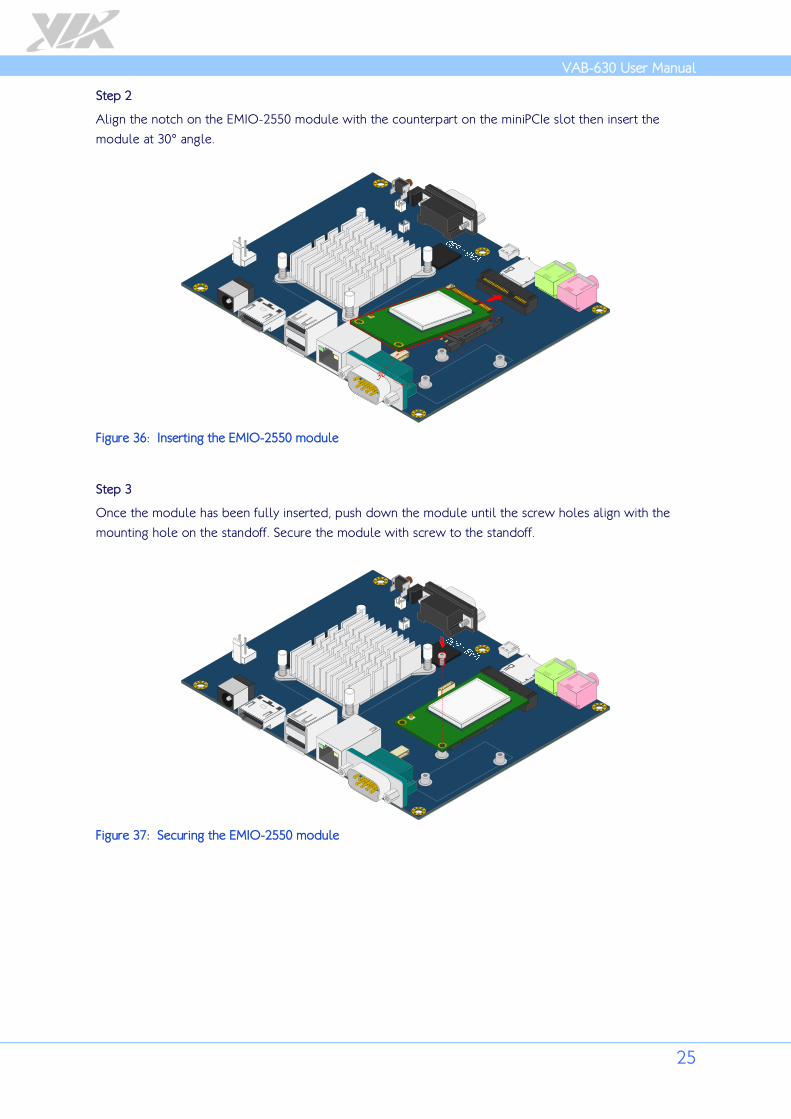
Step 2
Align the notch on the EMIO-2550 module with the counterpart on the miniPCIe slot then insert the
module at 30° angle.
ÑÒÓÔÕÖ×
LOCK
OPEN
30
Figure 36: Inserting the EMIO-2550 module
Step 3
Once the module has been fully inserted, push down the module until the screw holes align with the
mounting hole on the standoff. Secure the module with screw to the standoff.
ØÙÚÛÜÝÞ
LOCK
OPEN
Figure 37: Securing the EMIO-2550 module

VAB-630 User Manual
26
Step 4
Insert the 3G antenna cable into the antenna hole from the inside of the back panel plate. Insert the
washer, fasten it with the nut and install the external antenna.
1
2
3 4
Figure 38: Connecting the antenna cable and antenna
Step 5
Gently connect the other end of the 3G antenna cable to the micro-RF connector labeled “MAN” on the
EMIO-2550 module.
ßàáâãäå
LOCK
OPEN
Figure 39: Connecting the antenna (to the micro-RF connector)

VAB-630 User Manual
27
A.2. Installing the EMIO-2531 miniPCIe Wi-Fi & Bluetooth
module
Step 1
Align the notch on the EMIO-2531 module with the counterpart on the miniPCIe slot then insert the
module at 30° angle.
æçèéêëì
LOCK
OPEN
30
Figure 40: Inserting the EMIO-2531 module
Step 2
Once the module has been fully inserted, push down the module until the screw holes align with the
mounting hole on the standoff. Secure the module with screw to the standoff.
íîïðñòó
LOCK
OPEN
Figure 41: Securing the EMIO-2531 module

VAB-630 User Manual
28
Step 3
Insert the Wi-Fi antenna cable into the antenna hole from the inside of the back panel plate. Insert the
washer, fasten it with the nut and install the external antenna.
1
2
3
4
Figure 42: Connecting the Wi-Fi antenna cable and antenna
Step 4
Gently connect the other end of the Wi-Fi antenna cable to the micro-RF connector labeled “MH2” on the
EMIO-2531 module.
ôõö÷øùú
LOCK
OPEN
Figure 43: Connecting the antenna cable to the micro-RF connector

VAB-630 User Manual
29
A.3. Installing EMIO-5531 USB Wi-Fi module
Step 1
Mount the EMIO-5531 module on the VAB-630 mainboard. Align the module’s mounting holes with the
standoff screw holes on the mainboard then secure it with two screws.
ûüýþÿV�
LOCK
OPEN
2
1
Figure 44: Installing and securing EMIO-5531 module
Step 2
Attach the USB Wi-Fi cable (P/N 99G33-193126) to the connector on EMIO-5531 module, and then attach
the other end of the cable to the onboard USB Wi-Fi connector (JUSB1) on the VAB-630 mainboard.
�������
LOCK
OPEN
2
1
LOCK
Figure 45: Connecting USB Wi-Fi cable

VAB-630 User Manual
30
Step 3
Insert the Wi-Fi antenna cable into the antenna hole from the inside of the back panel plate. Insert the
washer, fasten it with the nut and install the external antenna.
1
2
3
4
Figure 46: Connecting the antenna cable and antenna
Step 4
Gently connect the other end of the Wi-Fi antenna cable to the micro-RF connector labeled “MH2” on the
EMIO-5531 module.
��
� �
LOCK
OPEN
Figure 47: Connecting the antenna cable to the micro-RF connector
VAB-630 User Manual
31
Appendix B. Installing LVDS Panel Display
B.1. Connecting the LVDS Panel Display to the VAB-630
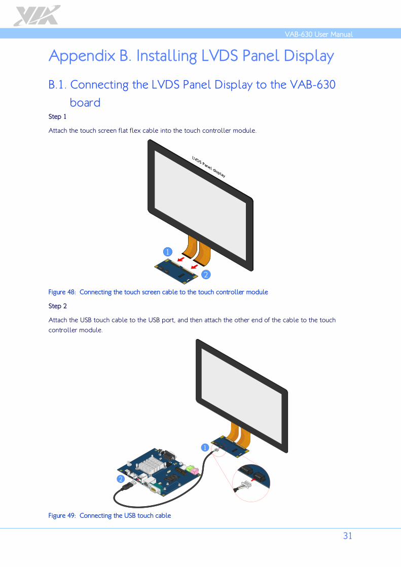
board Step 1
Attach the touch screen flat flex cable into the touch controller module.
LVDS Panel display
2
1
LVDS Panel display
2
1
Figure 48: Connecting the touch screen cable to the touch controller module
Step 2
Attach the USB touch cable to the USB port, and then attach the other end of the cable to the touch
controller module.
�������
LOCK
OPEN
1
2
Figure 49: Connecting the USB touch cable

VAB-630 User Manual
32
Step 3
Connect the flex flat cable connector to the LVDS panel display backside and then into the VAB-630
backside of the mainboard. The blue color side of the LVDS cable must face up when connecting to the
LVDS panel (both panel and board).
LVDS Pan
el disp
lay
(���
� ����
�
2
1
Figure 50: Connecting the flex flat cable
Step 4
For LVDS panel u-boot setting refers to VAB-630_Andriod5.0_BSP_Quick_Start_Guide_v1.0.0 section
5.1.2 setting up the LVDS Up and LVDS U-Boot display parameter.
VAB-630 User Manual
33
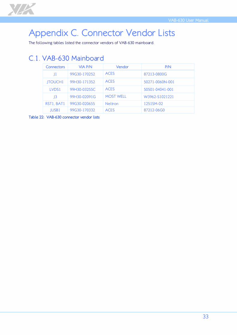
Appendix C. Connector Vendor Lists The following tables listed the connector vendors of VAB-630 mainboard.
C.1. VAB-630 Mainboard Connectors VIA P/N Vendor P/N
J1 99G30-170252 ACES 87213-0800G
JTOUCH1 99H30-171352 ACES 50271-0060N-001
LVDS1 99H30-03255C ACES 50501-04041-001
J3 99H30-02091G MOST WELL W3962-S1021221
RST1, BAT1 99G30-020655 Neltron 1251SM-02
JUSB1 99G30-170332 ACES 87212-06G0
Table 22: VAB-630 connector vendor lists


![[XLS] · Web view400 630 630 400 630 990 990 630 630 630 630 990 990 990 990 990 990 400 400 990 630 990 630 630 400 990 990 990 990 990 630 630 990 990 630 630 990 990 990 990 990](https://static.fdocuments.us/doc/165x107/5af695027f8b9a5b1e8f4d8f/xls-view400-630-630-400-630-990-990-630-630-630-630-990-990-990-990-990-990-400.jpg)