User Manual programable power Supply
109
SL Series User Manual Programmable DC Power Supply M AGNA-POWER ELECTRONICS M E P Higher Quality Power Processing
description
User Manual programable power Supply
Transcript of User Manual programable power Supply

SL Series User ManualProgrammable DC Power Supply
MAGNA-POWERELECTRONICS
MEP
Higher Quality Power Processing

User Manual
SL Series 1 User ManualAuthor Magna-Power Electronics [email protected]
Copyright © 2012 Magna-Power Electronics, Inc. All Rights Reserved.
Magna-Power Electronics® is a registered trademark of Magna-Power Electronics, Inc.
All other trademarks are the property of their respective owners.
39 Royal Road Flemington, NJ 08822 USA Phone: +1-908-237-2200 Fax: +1-908-237-2201 [email protected]
This User Manual provides installation instructions, operating procedures, and product specificationsfor the SL Series programmable DC power supply. Contents of this User Manual are subject to changewithout notice.

iii
Preface v1. Safety Notice .................................................................................................................. v2. Limited Warranty ............................................................................................................. v
2.1. Claim for Damage in Shipping .............................................................................. vi2.2. Returning Equipment ........................................................................................... vi
3. Declaration of Conformity ................................................................................................ vi4. Document Conventions .................................................................................................. vii
4.1. Notes and Warnings ............................................................................................ vii4.2. Text Conventions ................................................................................................ vii
5. Getting Help and Giving Feedback ................................................................................ viii5.1. Additional Support .............................................................................................. viii5.2. Feedback ........................................................................................................... viii
1. Product Information 11.1. Key Features ............................................................................................................... 11.2. Principle of Operation ................................................................................................... 21.3. Specifications ............................................................................................................... 31.4. Models ......................................................................................................................... 61.5. Diagrams and Indicators ............................................................................................... 71.6. Product Options ........................................................................................................... 9
1.6.1. High Isolation Output (+ISO) .............................................................................. 91.6.2. High Slew Rate Output (+HS) ............................................................................ 91.6.3. IEEE-488 GPIB Interface (+GPIB) .................................................................... 131.6.4. LXI TCP/IP Ethernet Interface (+LXI) ................................................................ 131.6.5. UID47: Universal Interface Device (+UID) ......................................................... 131.6.6. USB Edgeport (+USB) ..................................................................................... 141.6.7. Water Cooling (+WC) ....................................................................................... 14
2. Installation 152.1. Product Inspection ...................................................................................................... 152.2. Rack Installation and Cooling ...................................................................................... 152.3. AC Input Connections ................................................................................................. 152.4. DC Output Connections .............................................................................................. 17
2.4.1. Remote Voltage Sensing .................................................................................. 172.5. Electrical Check ......................................................................................................... 18
2.5.1. Electrical Check for Models with SL Version Front Panel .................................... 192.5.2. Electrical Check for Models with C Version Front Panel ...................................... 19
3. Operation 213.1. Output Regulation Modes ........................................................................................... 21
3.1.1. Constant Voltage ............................................................................................. 213.1.2. Constant Current ............................................................................................. 213.1.3. Pulse Loading ................................................................................................. 21
3.2. Front Panel Commands .............................................................................................. 223.2.1. Run Mode Commands ..................................................................................... 223.2.2. Set Point Commands ....................................................................................... 233.2.3. Configuration Commands ................................................................................. 243.2.4. Calibration Commands ..................................................................................... 26
3.3. External 37-pin (JS1) I/O Programming and Operation .................................................. 273.3.1. External 37-pin I/O Pin Definitions .................................................................... 283.3.2. External Analog Programming .......................................................................... 313.3.3. External Analog Monitoring .............................................................................. 333.3.4. Digital Input Lines ............................................................................................ 333.3.5. Digital Output Lines ......................................................................................... 34
3.4. Parallel and Series Operation ..................................................................................... 35
User Manual
iv
3.4.1. Parallel Operation ............................................................................................ 353.4.2. Series Operation .............................................................................................. 37
3.5. Troubleshooting Guide ................................................................................................ 393.6. Calibration .................................................................................................................. 40
3.6.1. Contol Board ................................................................................................... 403.6.2. Driver Board .................................................................................................... 41
4. Remote Interface Software 434.1. Application Setup ....................................................................................................... 434.2. Virtual Control Panel .................................................................................................. 454.3. Command Panel ........................................................................................................ 454.4. Register Panel ........................................................................................................... 464.5. Calibration Panel ........................................................................................................ 474.6. Firmware Panel .......................................................................................................... 484.7. Modulation Panel ....................................................................................................... 49
5. Computer Programming 515.1. SCPI Commands ........................................................................................................ 51
5.1.1. Parameter Data Types ..................................................................................... 515.1.2. Restricted SCPI Command Set ........................................................................ 525.1.3. Calibration Commands ..................................................................................... 545.1.4. Configuration Commands ................................................................................. 565.1.5. Measure Commands ........................................................................................ 595.1.6. Modulation Commands .................................................................................... 595.1.7. Output Commands ........................................................................................... 625.1.8. Source Commands .......................................................................................... 645.1.9. Status Commands ........................................................................................... 685.1.10. System Commands ........................................................................................ 705.1.11. Trigger Commands ......................................................................................... 71
5.2. RS232 Communications ............................................................................................. 725.3. IEEE-488 GPIB Communications ................................................................................ 73
5.3.1. IEEE-488 GPIB Communication using the Remote Interface Software ................. 745.3.2. IEEE-488 GPIB Communications with MAX ....................................................... 745.3.3. IEEE-488 GPIB SCPI Commands and Registers ............................................... 75
5.4. LXI TCP/IP Ethernet Communications ......................................................................... 805.4.1. Connectivity and IP Address Negotiation ........................................................... 815.4.2. LXI TCP/IP Ethernet Control and Discovery Methods ......................................... 825.4.3. LXI TCP/IP Ethernet SCPI Commands .............................................................. 86
5.5. USB Communications ................................................................................................. 895.5.1. USB Edgeport/1 Setup ..................................................................................... 905.5.2. USB Edgeport/1 Communications Using the Remote Interface Software .............. 90
5.6. RS485 Communications ............................................................................................. 905.6.1. 485DSS Initial Setup ........................................................................................ 91
5.7. IVI-COM Driver .......................................................................................................... 92
6. Applications 936.1. Power Waveform Generation ...................................................................................... 936.2. Leadless Remote Sensing .......................................................................................... 946.3. Photovoltaic Cell Simulator ......................................................................................... 946.4. Battery Charger .......................................................................................................... 956.5. Constant Power Operation .......................................................................................... 98
A. Revision History 101

v
Preface
1. Safety NoticeBefore applying power to the system, verify that the unit is configured properly for the user’s particularapplication.
CE recognition of SL Series programmable DC power supplies is based on rack-mounted applicationsonly. Use of these power supplies outside of a rack mount equipment enclosure will expose the user tohigh voltage and/or high current sources. Extreme caution must be used under these circumstances.
Two or more SL Series programmable DC power supplies may be connected in series. Regardless ofthe number of units or the voltage ratings of the series connected power supplies, the voltage potentialfrom any output terminal to chassis ground should not exceed the product's isolation rating of ±1000Vdc..
Installation and service must be performed only by properly trained and qualified personnel who areaware of dealing with electrical hazards. Ensure that the AC power line ground is properly connectedto the power supply chassis. Furthermore, other power grounds, including those connected toapplication maintenance equipment, must be grounded for both personnel and equipment safety.
Always ensure that facility AC input power is de-energized prior to connecting or disconnecting theinput and output power cables.
Caution: Lethal voltages may be present inside the power supply even when the ACinput voltage is disconnected. Only properly trained and qualified personnel shouldremove covers and access the inside of the power supply.
During normal operation, the operator does not have access to hazardous voltages within the cabinet.Depending on the user’s application, high voltages hazardous to human safety may be generatednormally on the output terminals. Ensure that the output power cables are properly labeled as to thesafety hazards and that any inadvertent contact with hazardous voltages is eliminated.
This power supply is designed to be permanently connected to the power source requiring a readilyaccessible disconnect device incorporated in the fixed wiring.
These operating instructions form an integral part of the equipment and must be available to theoperating personnel at all times. All the safety instructions and advice notes are to be followed.
Neither Magna-Power Electronics, Inc. nor any of the associated sales organizations can acceptresponsibility for personal injury, consequential injury, loss, or damage resulting from improper use ofthe equipment and accessories.
2. Limited WarrantyThe following is made in lieu of all warranties expressed or implied.
Magna-Power Electronics, Inc. warranties its products to be free of manufacturing defects for a periodof two (2) years from date of original shipment from its factory. Magna-Power Electronics, Inc. willrepair, replace, or refund the purchase price at its discretion, which upon examination by Magna-Power Electronics, Inc., is determined to be defective in material or workmanship, providing suchclaimed defective material is returned upon written authorization of Magna-Power Electronics, Inc.,freight prepaid.
For products failing within the first 30 days of the warranty period, Magna-Power Electronics, Inc.will return the repaired product at its expense using a standard shipping method; after 30 days of the
SIU850550361
Highlight
SIU850550361
Highlight
SIU850550361
Highlight

Preface
vi
warranty period, the repaired product will be returned at the customer's expense using the customer'srequested shipping method.
Damage due to corrosion, customer alterations, excessive dust, extreme environmental or electricalconditions, and/or misuse will be evaluated upon inspection. If inspection reveals that the cause ofdamage is not due to materials or workmanship, repair of the product will be treated on a non-warrantybasis.
All electrical, commercial supply parts, and items not manufactured by Magna-Power Electronics,Inc. shall carry the warranty of the original manufacturer and no more, but under no circumstances toexceed the warranty period. Replacement parts shall be warranted for a period of 90 days.
Warranty labor shall only apply if the product, assembly, or part is returned to the factory freightprepaid and insured. Damage or breakage while in transit is not covered by this warranty.
Magna-Power Electronics, Inc. assumes no responsibility to Buyer for labor to diagnose and removedefective product and installation of replacement product. Furthermore, Magna-Power Electronics,Inc. is not liable to Buyer or to any third party for consequential or incidental damages under anycircumstances, whether due to defect in the product, due to delay or failure of delivery, due to a failureof the product to perform as specified, or for any other reason or cause. Buyer and Magna-PowerElectronics, Inc. agree that Buyer's sole remedy and Magna-Power Electronics, Inc.'s sole liability toBuyer is limited to repair, replacement, or refund of the purchase price of the product as describedherein, whether Buyer's claim arises out of contract or in tort.
All claims against the warranty shall be the final determination of Magna-Power Electronics, Inc.
2.1. Claim for Damage in ShippingThis instrument received comprehensive mechanical and electrical inspections before shipment.Immediately upon receipt from the carrier, and before operation, this instrument should be inspectedvisually for damage caused in shipment. If such inspection reveals internal or external damage in anyway, a claim should be filed with the carrier. A full report of the damage should be obtained by theclaim agent and this report should be forwarded to us. We will then advise you of the disposition tobe made of the equipment and arrange for repair or replacement. When referring to this equipment,always include the model and serial numbers.
2.2. Returning EquipmentBefore returning any equipment to the factory, the following steps should be observed:
• Contact our technical service department or file a RMA request (http://www.magna-power.com/support/rma-request). Give a full description of the difficulty and include the model and serialnumber of the unit. Upon receipt of this information, we will give you service information or shippinginstructions.
• Packaging and method of shipment must be coordinated with the factory to insure safe delivery.All equipment returned for repair requires a Return Authorization Number and must be insured. Noreturns will be accepted without assignment of a Return Authorization Number.
• For non-warranty repairs, we will submit a cost estimate for your approval before proceeding.
3. Declaration of ConformityThe Declaration of Conformity is included with all products on the calibration certificate. An additionaldigital copy is available by request at no charge for all Magna-Power Electronics products. To receive
Document Conventions
vii
an additional digital copy of the product's Declaration of Conformity, email your product's serial numberto [email protected]
4. Document ConventionsThis user's manual uses several conventions to highlight certain words and phrases and drawattention to specific pieces of information.
In PDF and paper editions, this manual uses typefaces drawn from the Liberation Fonts1 set. TheLiberation Fonts set is also used in HTML editions if the set is installed on your system. If not,alternative but equivalent typefaces are displayed.
4.1. Notes and Warnings
Note
Notes are tips, shortcuts or alternative approaches to the task at hand. Ignoring a note shouldhave no negative consequences, but you might miss out on a time saving procedure.
4.1.1. Safety SymbolsTable 1, “ Safety Symbols” defines the IEC symbols used throughout this Users Manual for the SLSeries.
Table 1. Safety SymbolsSymbol Definition
Earth ground, protective conductor terminal
Caution, risk of electric shock
Caution, risk of danger
Three-phase alternating current
4.2. Text ConventionsSource-code listings are also set in mono-spaced roman but add syntax highlighting as follows:
package org.jboss.book.jca.ex1;
1 https://fedorahosted.org/liberation-fonts/

Preface
viii
import javax.naming.InitialContext;
public class ExClient{ public static void main(String args[]) throws Exception { InitialContext iniCtx = new InitialContext(); Object ref = iniCtx.lookup("EchoBean"); EchoHome home = (EchoHome) ref; Echo echo = home.create();
System.out.println("Created Echo");
System.out.println("Echo.echo('Hello') = " + echo.echo("Hello")); }}
Terms and definitions are highlighted as follows:
Sample title for reference and definition listSample Term
Sample Definition
5. Getting Help and Giving Feedback
5.1. Additional SupportIf you experience difficulty with a procedure described in this documentation, visit the Magna-PowerElectronics Support Portal at http://www.magna-power.com/support. Through the Support Portal, youcan:
• Search or browse through a knowledge base of technical support articles about Magna-PowerElectronics products
• Access the most up-to-date searchable and browseable product documentation, such as this User'sManual
• Review application notes and guides for key product applications
5.2. FeedbackIf you find a typographical error in this manual, or if you have an idea how to make this manual better,we would like to hear from you. Please submit an email report to: [email protected] againstthe product SL Series.
When submitting a bug report, be sure to mention the manual's identifier: SL Series User Manual
If you have a suggestion for improving the documentation, try to be as specific as possible whendescribing it. If you have found an error, please include the section number and some of thesurrounding text so we can find its location.

Chapter 1.
1
Product InformationThis chapter introduces the technology behind the SL Series Programmable DC Power Supply
1.1. Key FeaturesMagna-Power Electronics SL Series combines the best of DC power processing with microprocessorembedded control. Magna-Power Electronics innovative power processing technology improvesresponse, shrinks package size, and reduces cost. SL Series power supplies are current-fed and aremore tolerant to abusive loads than conventional switching power supplies.
SL Series power supplies can operate as a voltage source or a current source depending on thecontrol settings and load conditions. If the power supply is operating as a voltage source and the loadincreases to a point beyond the current command setting, the power supply automatically crosses overto current mode control and operates as a current source at that setting.
SL Series power supplies incorporate an optically isolated feedback system. The result is that all userinterface circuitry is referenced to earth ground, not the negative terminal of the power supply. Thisenables users to connect external circuitry without concern of ground loops or voltage breakdown, upto the full isolation rating of the power supply.
SL Series power supplies offer both master/slave parallel and series operation. This enables two ormore power supplies to be placed in parallel for increased output current or in series for increasedoutput voltage. With master/slave operation, power supplies operate at near equal voltage and current.
SL Series power supplies can be configured through the front panel for different applications. Thepower supply can be programmed to have its control functions accessible from the front panel,rear 37-pin connector, or with RS232, IEEE-488 GPIB (+GPIB), or LXI TCP/IP Ethernet (+LXI)communications. External RS485 to RS232 (+RS485) and external USB to RS232 (+USB) convertersare also available to echo commands over the communications network. Communication optionsmust be specified at time of order. SL Series power supplies support a full set of SCPI commands. IVIdrivers are available which support programming in Visual C++, Visual C#, Visual Basic .NET, VisualBasic 6.0, LabVIEW, LabWindows/CVI, MATLAB, Measure Foundry, and Agilent VEE Pro.
Sensing can be established at the output terminal of the power supply or through a rear terminal blockfor remote sensing at the load. A smart remote sense detector checks whether or not sense leads arepresent eliminating the potential of uncontrolled operation. An external interlock can be set to enableoperation only when an external connection is made. Even calibration has been simplified with frontpanel access to calibration digital potentiometers.
SL Series power supplies have three levels of over voltage/current protection: shutdown of controllinginsulated gate bipolar transistors (IGBTs), disconnect of main power, and input fuses. After an overvoltage/current trip condition, the supply must be reset using the Clear functionality.
SL Series power supplies have push button start/stop controls. These controls are tied to amechanical contactor which operates with the electronic switches to break the AC mains when stop iscommanded. Off means both an electrical and mechanical break in the power circuit—not just a breakin an electronic switch. Safety comes first at Magna-Power Electronics.
SL Series power supplies are available with two alternative front panels: SL Version for analog/digitalcontrol and C Version for computer or programmable logic control. All SL Series power suppliesemploy the same power processing engine.
SL Series models utilizing the SL Version front panel provide stepless analog control from front panelpotentiometers. With simple configuration changes, voltage, current, over voltage trip, and over currenttrip may be programmed from the 37-pin isolated I/O, RS232, IEEE-488 GPIB (+GPIB), LXI TCP/IP
SIU850550361
Highlight
SIU850550361
Highlight
SIU850550361
Highlight
SIU850550361
Highlight
SIU850550361
Highlight
SIU850550361
Highlight
SIU850550361
Highlight
SIU850550361
Highlight
SIU850550361
Highlight
SIU850550361
Highlight
SIU850550361
Highlight
SIU850550361
Highlight
SIU850550361
Highlight
SIU850550361
Highlight
SIU850550361
Highlight
SIU850550361
Underline
SIU850550361
Highlight
SIU850550361
Sticky Note
Unmarked set by SIU850550361

Chapter 1. Product Information
2
Ethernet (+LXI), Edgeport USB (+USB). SL Series power supplies with SL Version front panels arewell suited for industrial and laboratory applications.
SL Series power supplies with the SL Version front panels offer an analog input to modulate thevoltage or current setting using piecewise linear approximation. This feature enables the voltage orcurrent setting to be adjusted by a sensor input, such as a thermistor, or by monitoring its own voltageor current. Modulation allows the output to be tailored for advanced process control applications,battery charging, and source emulation.
SL Series models utilizing the C Version front panel only allow control from the 37-pin isolated I/O, RS232, IEEE-488 GPIB (+GPIB), LXI TCP/IP Ethernet (+LXI), or Edgeport USB (+USB). Thesemodels are intended for process control applications where front panel controls and displays are notrequired or desired.
Remote Interface Software is included to provide sophisticated computer control. This softwareprovides a virtual control panel to emulate the power supply's front panel, a command panel to sendand monitor SCPI commands, a register panel to monitor registers, a calibration panel to provide easyaccess to calibrate digital potentiometers, a firmware panel to upgrade the control microprocessor, anda modulation panel to easily program modulation parameters.
SL Series models have extensive diagnostic functions—all of which when activated take commandto shut down the system. Diagnostic functions include phase loss, excessive thermal conditions, overvoltage trip, over current trip, and program line. Program line monitors externally applied analog setpoint signals to insure they are within the specified range. Upon a diagnostic fault condition, mainpower is disconnected and the diagnostic condition is latched into memory. Pressing the clear keyclears the memory. All diagnostic functions can be monitored through a rear connector. Furthermore,control functions can also be set through the rear connector to allow simultaneous control of one ormore SL Series units.
Finally, SL Series models rated for 16 Vdc and above have a novel electronic output stage that utilizesnear constant power loading under all conditions via an electronic bleed resistance. This electronicbleeder means stability under all operating conditions and faster fall times, without affecting the overallsystem efficiency.
1.2. Principle of OperationThis section provides a general overview of the technology and power processing stages in a Magna-Power Electronics SL Series. Figure 1.1, “SL Series functional block diagram” provides an visualoverview of the power supply's main power and control stages.
Power is fed through AC fuses and is distributed to the auxiliary power supply, inrush limiter, and main3Φ contactor. The auxiliary power supply operates off the AC mains, supplying power to the otherprinted circuit boards in the system. The inrush limiter is a step start device which is used to initiallycharge capacitors on the input DC bus and limit the inrush of current. The inrush limiter is initiatedwhen the power supply is switched from a standby to a power state. After the charge cycle, the main3Φ contactor is energized and power is allowed to flow to the load. The EMI filter reduces commonmode and differential mode noise emanating from the supply.
Output power is controlled through a polyphase chopper. For the 4 kW SL Series power supplies,three choppers, phased 120° apart, provide a current source to a current fed inverter. The 2.6 kWSL Series power supplies uses two choppers, phased 180° apart, and the 1.5 kW supplies usesonly one chopper. The choppers are controlled with current mode, pulse width modulation (PWM).This modulation scheme provides a quick response for transients and filtering harmonics on theDC bus. As illustrated, chopper output current is monitored for balancing and for sensing overloadcurrent conditions. The polyphase chopper has been engineered to eliminate harmonic componentsminimizing currents circulating in the power supply.
SIU850550361
Highlight
SIU850550361
Highlight
SIU850550361
Highlight
SIU850550361
Highlight
SIU850550361
Highlight
SIU850550361
Highlight
SIU850550361
Highlight
SIU850550361
Highlight
SIU850550361
Highlight
SIU850550361
Highlight
SIU850550361
Highlight
SIU850550361
Highlight
SIU850550361
Highlight
SIU850550361
Highlight
SIU850550361
Highlight
SIU850550361
Highlight
SIU850550361
Highlight
SIU850550361
Highlight
SIU850550361
Highlight

Specifications
3
The polyphase chopper produces a controlled DC bus which is connected to DC link inductors andcurrent fed, IGBT inverter. The inverter, which operates above 20 kHz, excites the main transformer athigher than normal line frequencies. This operation produces ohmic isolation between the input andoutput of the power supply using a transformer of dramatically reduced size.
The inverter operates with a 50% duty cycle and its frequency operation is transparent to theperformance of the power supply.
The output of the main power transformer is converted to DC via rectifiers. Low voltage versions ofthe SL Series power supply use midpoint diode configurations and higher voltage versions use bridgeconfigurations.
The DC output voltage is filtered with a pie section filter. This, in combination with the DC linkinductors, form a double stage inductive capacitive (LC) filter.
The gate driver board supports a synchronized modulation scheme which integrates powersemiconductor switching of the switching power supply, polyphase chopper, and IGBT inverter.
The phase detector senses input line voltage on each phase. Upon detection of a problem, the controlboard is signaled to shutdown the system. The control board, which is referenced to earth ground,contains optically isolated amplifiers to sense output voltage and current. This circuitry allows theoutput to be referenced ±1000 Vdc above earth ground.
The display board contains light-emitting diodes for displaying diagnostic conditions and provides aninterface for meters and switches.
Figure 1.1. SL Series functional block diagram
1.3. SpecificationsThis section details the product specifications for the SL Series. If additional product specifications arerequired, please contact Magna-Power Electronics by emailing [email protected]. Makesure to include your product's model and serial number along with your desired specification.
Specifications are subject to change without notice. For three-phase configurations, inputspecifications are line-to-line, specified at 208 Vac, 380 Vac, and 440 Vac input. Unless otherwisenoted input voltages and currents are specified for three-phase configurations.
Table 1.1. SL Series Physical Specifications
Physical Specifications
Power Size (H" x W" x D") Weight
1.5 kW 1.75 x 19 x 24 in (4.44 x 48.3 x 61.0 cm) 32 lbs. (14.52 kg)
2.6 kW 1.75 x 19 x 24 in (4.44 x 48.3 x 61.0 cm) 34 lbs. (15.42 kg)
4 kW 1.75 x 19 x 24 in (4.44 x 48.3 x 61.0 cm) 34 lbs. (15.88 kg)
SIU850550361
Highlight
SIU850550361
Highlight

Chapter 1. Product Information
4
Table 1.2. SL Series Input Specifications
Input Specifications
Nominal Voltage 1 phase, 2wire + ground
85 - 265 Vac, 1Φ (UI—Universal input)(Available on 1.5 kW Models Only)
Nominal Voltage3 phase, 3 wire + ground
208 Vac, 3Φ (operating range 187 - 229 Vac)240 Vac, 3Φ (operating range 216 - 264 Vac)380 Vac, 3Φ (operating range 342 - 418 Vac)415 Vac, 3Φ (operating range 373 - 456 Vac)440 Vac, 3Φ (operating range 396 - 484 Vac)480 Vac, 3Φ (operating range 432 - 528 Vac)
Frequency 50 Hz - 400 Hz (operating range 45 - 440 Hz)
Power Factor 99% at maximum power for 1Φ units> 92% at maximum power for 3Φ units
Table 1.3. SL Series Output Specifications
Output Specifications
Ripple (See Table 1.6, “SL Series Models”)
Line Regulation Voltage Mode: ±0.004% of full scaleVoltage Mode: ±0.02% of full scale
Load Regulation Voltage Mode: ±0.01% of full scaleCurrent Mode: ±0.04% of full scale
Load Transient Response 2 ms to recover within ±1% of regulated output, with a 50% to 100%or 100% to 50% step load change
Efficiency > 86% at full load (See Table 1.6, “SL Series Models”)
Stability ±0.10% for 8 hrs. after 30 min. warmup
Isolation Use inputs and outputs referenced to earth groundMaximum input voltage to ground ±2500 VacMaximum output voltage to ground ±1000 Vdc
Maximum Slew Rate Standard Models:100 ms for output voltage change from 0 to 63%100 ms for output current change from 0 to 63%With High Slew Rate Option (+HS):4 ms for output voltage change from 0 to 63%8 ms for output current change from 0 to 63%
Bandwidth Standard Models:3 Hz for remote analog voltage programming2 Hz for remote analog current programmingWith High Slew Rate Option (+HS):60 Hz for remote analog voltage programming45 Hz for remote analog current programming
Table 1.4. SL Series Control Specifications
Control Specifications
Voltage Programming Accuracy ±0.075% of full scale voltage
OVT Programming Accuracy ±0.075% of full scale voltage
Current Programming Accuracy ±0.075% of full scale current
OCT Programming Accuracy ±0.075% of full scale current

Specifications
5
Control Specifications
Voltage Readback Accuracy ±0.2% of full scale voltage
Current Readback Accuracy ±0.2% of full scale current
External Analog Programming andMonitoring Levels
0 - 10 Vdc
External Analog OutputImpedances
Voltage output monitoring: 100ΩCurrent output monitoring: 100Ω+10V reference: 1Ω
External Digital Programming andMonitoring Limits
Input: 0 to 5 Vdc, 10kΩ input impedanceOutput: 0 to 5 Vdc, 5 mA drive capacity
Remote Sense Limits 3% maximum voltage drop from output to load
Table 1.5. SL Series Environmental Specifications
Environmental Specifications
Ambient Operating Temperature 0°C to 50°C
Storage Temperature -25°C to 85°C
Humidity Relative humidity up to 95% non-condensing
Temperature Coefficient 0.04 %/°C of maximum output voltage0.06 %/°C of maximum output current
Air Flow Side air inlet, rear exhaust
SL Series Agency ApprovalsEN61010-1:2010-02
Safety Requirements for Electrical Equipment for Measurement, Control, and Laboratory Use
2004/108/ECEMC Directive
EN61000-6-3 and EN61000-6-3General Emissions Standard
EN55022 Class AProduct Specifications Emissions
EN61000-6-1Generic Immunity Standard, including the following cross references: EN61000-4-2 (ElectrostaticDischarge), EN61000-4-3 (Radiated Susceptibility), EN61000-4-4 (Electrical Fast Transient/Burst),EN61000-4-6 (Conducted Susceptibility), EN61000-4-8 (Magnetics), EN61000-4-11 (Voltage Dipsand Interruptions)

Chapter 1. Product Information
6
1.4. Models
Figure 1.2. SL Series model ordering guide
Table 1.6, “SL Series Models” details the available standard SL Series models. The Current Maximum(Adc) column is separated by the available power levels. To determine the appropriate model, firstselect your output Voltage Maximum (Vdc) to find appropriate row. Next, select one desired CurrentMaximum from the row that contains your desired Voltage Maximum. Then, construct you modelnumber according to the Figure 1.2, “SL Series model ordering guide”. Non-standard voltage andcurrent configurations are available.
Table 1.6. SL Series Models
1.5 kW 2.6 kW 4 kW
Voltage Maximum(Vdc)
Current Maximum (Adc) Ripple(mVrms)
Efficiency(%)
5 250 N/A N/A 50 86
10 150 250 N/A 40 86
16 93 162 250 35 86
20 75 130 200 40 86
32 46 81 125 40 86
40 37 65 100 40 87
50 30 52 80 50 87
80 18 32 50 60 87
100 15 26 40 60 87
125 12 20 32 100 87
160 9 16 25 120 87
200 7 13 20 125 87
250 6 10.4 16 130 88
375 4 6.9 10.4 170 88
400 3.7 6.5 10 180 88
500 3 5.2 8 220 88
600 2.5 4.3 6.4 250 88
800 1.8 3.2 4.8 300 88
1000 1.5 2.6 4.0 350 88
Maximum Input Current (Aac)
UI (85 - 265 Vac, 1Φ) 21 - 7 N/A N/A
208/240 Vac, 3Φ 6 11 16

Diagrams and Indicators
7
Maximum Input Current (Aac)
380/415 Vac, 3Φ 5 8 11
440/480 Vac, 3Φ 4 6 9
1.5. Diagrams and IndicatorsThis section provides diagrams detailing the SL Series front panel layout and physical dimensions.The definitions for the diagram references are detailed in after the diagrams.
Figure 1.3. SL Version front panel layout
Figure 1.4. SLC Version front panel layout
Figure 1.5. SL Version front panel dimensions
Figure 1.6. SL Series rear panel layout and dimensions
Figure 1.7. SL Series top panel layout and dimensions, rear side
Figure 1.8. SL Series side panel layout and dimensions
SIU850550361
Highlight
SIU850550361
Highlight

Chapter 1. Product Information
8
Front Panel Definitions A (MODE)
POWER: Indicates power outputSTANDBY: Indicates control power only
B (FUNCTION KEYS)MENU: Selects functionITEM: Selects item within functionV/I DIS: Displays voltage/current settingsTRIP DIS: Displays OVT and OCT settingsCLEAR: Clears setting or resets faultENTER: Selects item
CMeters display output voltage, output current,voltage set point, current set point, overvoltage trip, and over current trip
DPower switch energizes control circuitswithout engaging main power
EEngages and disengages main power
FStepless rotary knob to set voltage/current
G (DIAGNOSTIC ALARMS)LOC: InterlockPGL: External input voltage beyond limitsPHL: Indicates under-voltage AC inputTHL: Indicates over-temperature conditionOVT: Over-voltage protection has trippedOCT: Over-current protection has tripped
H (CONFIGURATION)REM SEN: Remote sense enabledINT CTL: Front panel start/stop/clear enabledEXT CTL: External start/stop/clear enabledROTARY: Front panel controlEXT PGM: External voltage/current controlREMOTE: Computer control
Rear and Side Panel Definitions 1
Front Panel Handles (Removable)
2Remote Sense Connections
3Computer and External Control Connections
4Rear Air Exhaust
5Output DC Connections, 0.25" x 0.75" TinPlated Copper Bus, Qty (2) 3/8-16 ThreadedInsert
6Input AC Connections, 38660 Molex InputConnector
710-32 Ground Stud
8Side Air Intake
9Qty (2) Rear Metal Covers (Removable)
SIU850550361
Highlight
SIU850550361
Highlight
SIU850550361
Highlight
SIU850550361
Highlight
SIU850550361
Highlight

Product Options
9
37 19
120
5
1
9
6
(c)(a)
24 12
113
(d) (e)
1
8
1
2
(b)
Figure 1.9. SL Series communication connections: (a) JS1, external program interface; (b) JS2,remote sense; (c) JS3, RS232; (d) JS4, IEEE-488 GPIB; and (e) JS5, LXI TCP/IP Ethernet (viewedfrom female end)
1.6. Product OptionsThis sections provides details on all the available options for all Magna-Power ElectronicsProgrammable DC Power Supply products. Note that not all options may be available for the SLSeries.
1.6.1. High Isolation Output (+ISO)Certain applications require floating the output voltage to values beyond the power supply isolationrating. Magna-Power Electronics High Isolation Output Option (+ISO) enables any TS Series, MSSeries, or MT Series model with a peak output voltage rating of 250 Vdc through 1000 Vdc to berated for a higher voltage output isolation. Improved isolation is achieved by a novel output stage withimproved controller isolation. In addition to being able to float the power supply to a higher outputvoltage, this option also enables lower voltage units to be tied together in series up to the higherisolation rating.
Table 1.7, “(+ISO) Option Isolation Specifications” provides the output isolation rating for all availableconfigurations, where Vo is the unit's rated maximum output voltage.
Table 1.7. (+ISO) Option Isolation Specifications
Product Isolation, models1000 Vdc and below
Isolation, models1000 Vdc and belowwith +ISO option
Isolation, modelsabove 1000 Vdc
SL Series 1000 Vdc N/A N/A
XR Series 1000 Vdc N/A N/A
TS Series 1000 Vdc ±(2000 Vdc + Vo/2) ±(2000 Vdc + Vo/2)
MS Series 1000 Vdc ±(2000 Vdc + Vo/2) ±(2000 Vdc + Vo/2)
MT Series 1000 Vdc 4000 Vdc 4000 Vdc
1.6.2. High Slew Rate Output (+HS)The high slew rate option solves several limitations inherent in switching power supply design.Rapid voltage transitions require internal electronics to supply the energy to charge and discharge
SIU850550361
Highlight
SIU850550361
Highlight
SIU850550361
Highlight
SIU850550361
Highlight
SIU850550361
Highlight

Chapter 1. Product Information
10
output capacitors. Peak currents internal to the power supply define slew rate; utilizing lesscapacitance enables voltage transitions in shorter time periods. Additionally, less capacitance reducesrequirements for discharge demands during open circuit conditions.
The standard output stage Magna-Power Electronics power supplies has been designed to providethe lowest possible output ripple voltage within the constraints of available components, size, and cost.Part of the output stage consists of a bank of aluminum electrolytic capacitors which has the desiredelectrical properties to provide this function. These components require bleed resistors to dischargeany voltage when the power supply has no load and is disabled. While the presence of thesecomponents and the resulting performance are normally industry accepted, there are applicationswhere lower output capacitance is extremely desirable and higher ripple voltage is acceptable. Tomeet this need, a high-slew rate option is available which has an output stage consisting of lowcapacitance film and aluminum electrolytic capacitors. Applications for the high-slew rate optioninclude battery charging, photovoltaic emulation, power waveform generation, and medium speedpower pulsing. These applications all benefit from higher bandwidth and in many cases, can tolerateincreased ripple voltage.
For photovoltaic emulation applications, higher bandwidth and lower output capacitance enableimproved performance with higher speed, maximum power tracker algorithms. Maximum powertracker circuitry deviates the operating point of photovoltaic arrays to determine maximum poweroutput. Slow responding emulation sources can present a problem when the speed of the algorithmexceeds that of the source. Furthermore, with lower output capacitance, changes in the operatingpoint and transients, caused by shorting the solar inverter input, produce lower unwanted inputcurrents.
The high-slew rate option enables the power supply to operate as a low frequency, power pulsegenerator. With the special capacitors selected for this option, it is possible to superimpose waveformsor produce a medium speed pulse on top of the dc output and expect normal capacitor life. It isimportant to note that the power supply output is single quadrant; that is, the output voltage or currentcannot reverse.
The tables below define the High Slew Rate Output (+HS) option specifications.
Table 1.8. XR Series High Slew Rate Output Capacitance and Ripple
Output VoltageRange (Vdc)
Output Capacitance (uF) Output Ripple (mVrms)
5 13200 500
10 4080 750
16 4080 750
20 2340 1000
32 2340 1500
40 240 1500
50 240 1750
80 240 1750
100 160 2000
Note:
1. For 20 to 30 kW models, multiply capacitance by 2
2. For 45 kW models, multiply capacitance by 3.
3. For 60 kW models, multiply capacitance by 4
4. For 75 kW models, multiply capacitance by 5
SIU850550361
Highlight
SIU850550361
Highlight
SIU850550361
Highlight
SIU850550361
Highlight
SIU850550361
Highlight
SIU850550361
Highlight
SIU850550361
Highlight

High Slew Rate Output (+HS)
11
Output VoltageRange (Vdc)
Output Capacitance (uF) Output Ripple (mVrms)
125 160 2000
160 160 2500
200 160 2500
250 160 3000
375 160 3000
400 160 3000
500 56 3000
600 56 3500
800 56 3500
1000 52 3500
Note:
1. For 20 to 30 kW models, multiply capacitance by 2
2. For 45 kW models, multiply capacitance by 3.
3. For 60 kW models, multiply capacitance by 4
4. For 75 kW models, multiply capacitance by 5
Table 1.9. TS Series and MS Series High Slew Rate Output Capacitance and Ripple
Output VoltageRange (Vdc)
Output Capacitance (uF) Output Ripple (mVrms)
5 13200 750
8 9000 750
10 4080 750
16 4080 750
20 2340 1000
32 1170 1000
40 750 3500
50 750 3500
80 300 4000
100 200 4000
125 200 4500
160 200 4500
200 200 5000
250 200 5000
375 160 5500
Note:
1. For 20 to 30 kW models, multiply capacitance by 2
2. For 45 kW models, multiply capacitance by 3.
3. For 60 kW models, multiply capacitance by 4
4. For 75 kW models, multiply capacitance by 5

Chapter 1. Product Information
12
Output VoltageRange (Vdc)
Output Capacitance (uF) Output Ripple (mVrms)
400 160 5500
500 70 5500
600 60 6000
800 56 6000
1000 52 6000
1500 18 6500
2000 18 6500
3000 9 7000
4000 9 7000
Note:
1. For 20 to 30 kW models, multiply capacitance by 2
2. For 45 kW models, multiply capacitance by 3.
3. For 60 kW models, multiply capacitance by 4
4. For 75 kW models, multiply capacitance by 5
Table 1.10. MT Series High Slew Rate Output Capacitance and Ripple
Output VoltageRange (Vdc)
Output Capacitance (uF) Output Ripple (mVrms)
16 41000 1000
20 4100 1000
32 16000 1400
40 16000 1500
50 16000 1500
80 16000 1500
100 8000 1500
125 8000 1500
160 8000 1500
200 3650 1750
250 3650 1750
375 1450 2000
400 1450 2000
500 1450 2000
600 1450 2000
800 1280 2000
1000 1280 2000
Note:
1. For 500 kW models, multiply capacitance by 2
2. For 750 kW models, multiply capacitance by 3
3. For 1000 kW models, multiply capacitance by 4

IEEE-488 GPIB Interface (+GPIB)
13
Output VoltageRange (Vdc)
Output Capacitance (uF) Output Ripple (mVrms)
1250 320 3500
1500 320 3500
2000 320 3500
3000 160 4000
4000 160 4000
Note:
1. For 500 kW models, multiply capacitance by 2
2. For 750 kW models, multiply capacitance by 3
3. For 1000 kW models, multiply capacitance by 4
1.6.3. IEEE-488 GPIB Interface (+GPIB)The IEEE-488 GPIB interface, sometimes called the General Purpose Interface Bus (GPIB), is ageneral purpose digital interface system that can be used to transfer data between two or moredevices. It is particularly well-uited for interconnecting computers and instruments. Some of its keyfeatures are:
• Up to 15 devices may be connected to one bus
• Total bus length may be up to 20 m and the distance between devices may be up to 2 m
• Communication is digital (as opposed to analog) and messages are sent one byte (8 bits) at a time
• Message transactions are hardware handshaked
• Data rates may be up to 1 Mbyte/sec
1.6.4. LXI TCP/IP Ethernet Interface (+LXI)Certified to the LXI Standard (Class C), the TCP/IP Ethernet option includes an embedded web-server, allowing web browser power supply control and monitoring from virtually anywhere. LXI isan instrumentation platform based on industry standard Ethernet technology designed to providemodularity, flexibility, and performance to small- and medium-sized systems.
LXI's advantages are exemplified in its compact, flexible package providing high-speed I/O andreliable measurements. The Magna-Power Electronics LXI TCP/IP Ethernet option includes anembedded web-server, allowing web browser power supply control and monitoring from virtuallyanywhere.
1.6.5. UID47: Universal Interface Device (+UID)Magna-Power Electronics UID47 is a general purpose device for connection to Magna-PowerElectronics power supplies. The device contains the necessary circuitry for configuring power suppliesfor master/slave parallel or series operation.
Master/slave parallel operation allows two or more power supplies to equally share output currentwhen connected together. Master/slave series operation allows two or more power supplies toequally share output voltage when connected together. In either operation mode, the master unit willcommand the slave units to the proper voltage and current. Each unit will display its own individualvoltage and current. Installation requires setting jumpers, placing included 37-conductor cables

Chapter 1. Product Information
14
between the UID47 and power supplies, and wiring the power supply outputs in either parallel orseries.
The UID47 can be used as an interface for connecting control and monitoring lines to external circuitry.It also contains an area on the printed circuit board for interconnecting wires and placing componentsfor specific user applications. The key features for the UID47 are as follows:
• Compatible with all Magna-Power Electronics power supplies
• Plug and play interface for series and parallel master/slave operation
• User configurable screw terminal connector
• Pad area for custom circuitry
• (2) 6-foot 37-pin cables included
1.6.6. USB Edgeport (+USB)Edgeport USB-to-serial converters offer instant I/O expansion for peripheral device connectivity. Anout-of-the-box (external) alternative to PCI cards, Edgeport makes it easy to add serial port to a PC,server or thin client in minutes without opening the chassis, reconfiguring or rebooting the system.
The USB Edgeport device plugs directly into the back of the power supply, creating a seamless USBinterface. Feature-rich design, reliability and unmatched operating system support make EdgeportUSB-to-serial converters ideal for mission-critical enterprise applications. An USB cable is includedalong with associated drivers on the Magna-Power Electronics software CD.
1.6.7. Water Cooling (+WC)Water cooling is available for Magna-Power Electronics TS Series and MS Series power supplies. Thisoption is typically used in corrosive environments, such as electroplating applications or in denselypackaged system cabinets, where heat removal by air cooling presents a problem.
Water cooling is implemented with chill plates and an integrated central heat exchanger. The chillplates provides a thermal conduction path for heat sensitive components and the central heatexchanger removes heat from air internal to the enclosure. Water cooled TS Series models haveenclosures without vent holes and are basically sealed the unit from the environment. An internalsolenoid valve enables water flow when the chill plate reaches 60 degrees celcius. Operation of thesolenoid prevents internal condensation.
5 kW to 15 kW models have a 1/4" NPT male inlet and outlet for water flow. Models greater than 15kW have a 1/2" NPT male inlet and outlet for water flow with external plumbing that interconnectspower supply modules. A minimum of 2.50" is recommended behind the enclosure for this hardwareand user connections. For systems requiring more than one power supply, plumbing connections mustbe paralleled; that is, water should not flow from one power supply into another.
SIU850550361
Highlight
SIU850550361
Highlight

Chapter 2.
15
Installation
2.1. Product InspectionCarefully unpack the power supply saving all packing materials and included enclosures. Inspectpower supply for possible shipping damage. Check that there are no broken knobs or connectors, theexternal surface is not scratched or dented, the meter faces are not damaged, and all controls movefreely. Any external damage may be an indication of internal damage.
The following parts are included with all models:
• SL Series programmable DC power supply• RS232 cable• Rear metal cover with required fastening hardware• Printed SL Series user's manual• CD with software, drivers, and digital documentation• Calibration certificate with declaration of conformity
2.2. Rack Installation and CoolingSL Series power supplies are intended for rack mount installations only and are designed to fit instandard 19" equipment racks. Additional support, other than that provided by the front panel, isrequired. Angle slides or cross beam supports securely fastened to the rack are recommended forsupporting the weight of the power supply. The unit should be horizontally mounted.
Caution: The power supply is too heavy for one person to safely lift and mount. Toavoid injury, ask a co-worker for assistance.
Each programmable DC power supply is cooled by suitable fans exhausting warm air to the rear of thecabinet. Fresh air intake is from the sides of the cabinet allowing two or more SL Series supplies tobe stacked. Equipment racks should be equipped with fans or blowers to remove heat generated bythe power supplies. The manufacturer recommends fresh air intake at the bottom of the cabinet andexhaust at the top. Cabinet fans and blowers should be rated at 200 CFM for each SL Series supply.
Caution: Blocking ventilation will cause the power supply to overheat.
2.3. AC Input Connections
Caution: Disconnect AC power from the mains before attempting any installationprocedure.
Grounding: A safety ground wire must be connected to the unit as indicated by theprotective ground symbol at the rear of the power supply.
AC power is wired to the power supply by attaching three cables plus ground for 3-phase installationsor two cables and ground for single phase installations. The manufacture recommends cables, as
SIU850550361
Highlight
SIU850550361
Highlight
SIU850550361
Highlight

Chapter 2. Installation
16
specified in Table 2.1, “Suggested Ampacities of Conductors as Recommended by the NationalElectrical Code” or Table 2.2, “Suggested Ampacities of 4-Conductor Type S or SO Cable”, with oneend stripped of 1/2 inch (12.7 mm) of insulation and securely fastened to the 38660 Molex inputconnector at the rear of the power supply. After connections are made, the provided protective coversfor the AC input and DC output can optionally be installed and securely fastened to the chassisusing three screws per cover. This programmable DC power supply is designed to be permanentlyconnected to the power source requiring a readily accessible disconnect device incorporated into thefixed wiring.
Table 2.1. Suggested Ampacities of Conductors as Recommended by the National Electrical Code
Temprature Rating of Copper Conductor
60 °C 75 °C 85 °C 90 °C
Types Types Types Types
Wire Size (AWG) RUW, T, TW FEPW, RH, RH,RUH, THW,THWN, XHHW,ZW
V, MI TA, TBS, SA,AVB, SIS, FEP,FEPB, RHH,THHN, XHHW
14 25 30 30 35
12 30 35 40 40
10 40 50 55 55
8 60 70 75 80
6 80 95 100 105
4 105 125 135 140
3 120 145 160 165
2 140 170 185 190
1 165 195 215 220
1/0 195 230 250 260
2/0 225 265 290 300
3/0 260 310 335 350
4/0 300 360 390 405
250 MCM 340 405 440 455
300 MCM 375 445 485 505
350 MCM 420 505 550 570
Table 2.2. Suggested Ampacities of 4-Conductor Type S or SO Cable
Wire Size (AWG) Maximum Current (A)
18 7
16 10
14 15
12 20
10 25
8 35
6 45
4 60

DC Output Connections
17
Wire Size (AWG) Maximum Current (A)
2 80
2.4. DC Output Connections
Caution: Disconnect AC power from the mains before attempting any installationprocedure.
DC power is wired to the power supply by attaching two cables to the output bus bars. Magna-PowerElectronics recommends cables, as specified in Table 2.1, “Suggested Ampacities of Conductorsas Recommended by the National Electrical Code” or Table 2.3, “Suggested Ampacities of WeldingCable”, be crimped to ring terminals and securely fastened to bus bars using 3/8" bolts, washers, andlock washers. The bus bars contain 3/8"-16 threaded inserts. After connections are made, screw thefour standoffs into the back panel and place the protective shield over the connections.
Caution: Make sure connections are tight to avoid overheating of the bus bars.
Table 2.3. Suggested Ampacities of Welding Cable
Wire Size (AWG) Maximum Current (A)
6 85
4 110
3 130
2 150
1 170
1/0 200
2/0 235
3/0 275
4/0 315
* 315+
* Contact factory for assistance
2.4.1. Remote Voltage SensingRemote sensing is used to improve the degradation of regulation which will occur at the load whenthe voltage drop in the connecting wires is appreciable. Compensation is achieved by configuringthe power supply for remote sensing as described in Figure 3.4, “Enable or disable remote sensefunctionality”. Using a pair of #20 AWG wires, connect terminal 2 of JS2 to the positive terminal of theload and connect terminal 1 of JS2 to the negative terminal of the load. Table 2.4, “Remote Sense(JS2) Terminal Definition” defines the remote sensing pins and Figure 2.1, “(a) Local and (b) remotesensing” illustrates standard output sensing and remote output sensing.
Table 2.4. Remote Sense (JS2) Terminal Definition
Pin Definition
1 VO1REM-
SIU850550361
Highlight
SIU850550361
Highlight

Chapter 2. Installation
18
Pin Definition
2 VO1REM+
Caution: Switching remote sense leads or disconnecting remote sense leads while theoutput is enabled can cause device failure. Only switch or disconnect remote senseleads while the power supply is in standby or turned off.
Enabling remote sense activates the remote sense lead detector. The remote sense lead detectorchecks that the remote sense leads have been connected to the load. With the power supplyconfigured for remote sensing and upon enabling power output, the sense location is initially set tolocal. The sense location is switched to remote upon reaching 7.5% of full scale output voltage. If thevoltage detected is greater than 4.5% of full scale output voltage, the sense location remains remote; ifthe output voltage detected is less than 4.5%, then the sense location will automatically revert back tolocal.
The remote sense indicator on the front panel will flash when the remote sense functionality has beenenabled, but the power supply is remaining in local sense. The power supply will remain in local sensewith the REM SEN light flashing if the output voltage never exceeds 7.5% of full scale output voltageor the remote sense lead detector has determined sense leads are not connected. The remote senseindicator will remain flashing until the remote sense detector has detected the presence of remotesense voltage within the limits described above.
(b)
VO1REM-
VO1REM+
VS-
VS+
(a)
1
2
JS2
LOAD
VO-
VO+
MULTIPLEXER
MULTIPLEXER
VO+
VO-
LOAD
JS2
2
1
VS+
VS-
VO1REM+
VO1REM-
Figure 2.1. (a) Local and (b) remote sensing
2.5. Electrical CheckThis section describes the electrical checkout procedure for the SL Series. For SL Series unitspurchased with the standard SL Version front panel, refer to Section 2.5.1, “Electrical Check forModels with SL Version Front Panel”. For SL Series purchased with the C Version front panel, refer toSection 2.5.2, “Electrical Check for Models with C Version Front Panel”.

Electrical Check for Models with SL Version Front Panel
19
2.5.1. Electrical Check for Models with SL Version Front PanelWith the power supply off, disconnect the load, set voltage and current potentiometer controls fullycounterclockwise, and set the over voltage trip and over current trip settings to maximum, fullyclockwise. Connect the power supply to a suitable source of AC voltage. For this test, only 50% ofrated AC current is required. Turn the power switch on and observe the indicator lights going throughthe startup routine. After initialization, the following indicator lights should be on: STANDBY, INT CTL,EXT CTL, and ROTARY. This is the default configuration from the factory. It is recommended that thefollowing brief electrical check be made shortly after unpacking the supply.
Press the start switch and advance the current control one turn clockwise. The power and voltagecontrol indicators should light. Increase the voltage set point to maximum and then to minimum. DCvoltage should increase smoothly from minimum to maximum to minimum as indicated on the meter.Return the voltage control full counterclockwise. Press the stop switch.
To check over voltage trip, press the menu key. This places the power supply in data entry mode to setover voltage trip. Using the up/down arrow keys, enter an over voltage trip set point at half the ratingof the power supply. Once the over voltage trip set point has been entered, press the enter key to savethe information.
Press the start switch and slowly increase the voltage set point. Over voltage trip should operate at theover voltage trip set point. The over voltage trip (OVT) indicator should turn on, the power and voltagecontrol indicators should turn off, and the supply should shut down. Press the clear key. Now set theover voltage trip set point to maximum which is 110% the full scale rating of the power supply. Againstart the supply and observe that the power supply operates normally.
With the main power disconnected, connect a short to the power output terminals on the rear panel.Reconnect the main power, set voltage and current controls full counterclockwise, and turn the powerswitch on.
Press the start switch and advance the voltage control one turn clockwise. Increase the current setpoint to maximum and then to minimum. The power and current control indicators should light. DCcurrent should increase smoothly from minimum to maximum to minimum as indicated on the meter.Return the current control full counterclockwise. Press the stop switch.
To check over current trip, press the menu key and the item key one time. This places the powersupply in data entry mode to set over current trip. Using the up/down arrow keys, enter an over currenttrip set point at half the rating of the power supply. Once the over current trip set point has beenentered, press the enter key to save the information.
Press the start switch and slowly increase the current set point. Over current trip should operate at theover current trip set point. The over current trip (OCT) indicator should turn on, the power and currentcontrol indicators should turn off, and the supply should shut down. Press the clear key. Now set theover current trip set point to maximum which is 110% the full scale rating of the power supply. Againstart the supply and observe that the power supply operates normally.
If any of these events do not occur, the supply is defective and should not be operated. Depending onthe circumstances, either warranty service or trouble shooting is required.
2.5.2. Electrical Check for Models with C Version Front PanelThe electrical check for SL Series products with the C Version front panel models require use of theRemote Interface Software described in Chapter 4, Remote Interface Software. With the softwareinstalled and the power supply connected to the desired communications interface, select SL Versionin the Configuration Setup Panel. Select the Virtual Control Panel in the View Menu to display the SLVersion front panel. Follow the procedure outlined in Section 2.5.1, “Electrical Check for Models withSL Version Front Panel” using the Virtual Control Panel from within the Remote Interface Software.
SIU850550361
Highlight
SIU850550361
Highlight
SIU850550361
Highlight
SIU850550361
Highlight
SIU850550361
Highlight

20

Chapter 3.
21
OperationSL Series power supplies are normally shipped with its configuration set for rotary mode (frontpanel) input, local sensing, internal control, and external control. This configuration is set by frontpanel commands described in Section 3.2.3, “Configuration Commands” or by software. With thisconfiguration, the unit can operate in either constant voltage or a constant current output using thefront panel controls. SL Series power supplies with the C Version front panel are configured forexternal control and remote, enabling RS232, IEEE-488 GPIB (+GPIB), LXI TCP/IP Ethernet (+LXI), orEdgeport USB (+USB) communications. The front panel voltage and current controls set the boundarylimits for output voltage and current, respectively. The impedance of the load determines whether theunit is voltage or current controlled and the illumination of the respective mode indicator lights indicatethe state. The power supply will make a seamless autocrossover from voltage mode to current modecontrol, as warranted by the set-points and/or load impedance. If either control is set to maximumcounter clockwise rotation, the other control will have little or no effect, forcing either a zero voltage-limit or zero current-limit.
3.1. Output Regulation Modes
3.1.1. Constant VoltageTo select constant voltage output, proceed as follows:
With the supply off, set both rotary controls fully counterclockwise. Press the V/I DIS key and advancethe voltage and current controls for the desired output voltage and the desired crossover current. Thecrossover current is the current at which the power supply becomes a constant current source.
Connect the load and turn on the power supply. The output voltage should be close to the voltage setpoint. If a load change causes the current limit to be exceeded, the power supply will automaticallycrossover to constant current output at the preset current limit setting and the output voltage will dropproportionately. In setting the current limit, allowance must be made for high peak currents which cancause unwanted crossover.
3.1.2. Constant CurrentTo select constant current output, proceed as follows:
With the supply off, set both rotary controls fully counterclockwise. Press the V/I DIS key and advancethe voltage and current controls for the desired output current and the desired crossover voltage. Thecrossover voltage is the voltage at which the power supply becomes a constant voltage source.
Connect the load and turn on the power supply. The output current should be close to the current setpoint. If a load change causes the voltage limit to be exceeded, the power supply will automaticallycrossover to constant voltage output at the preset voltage limit setting and the output current will dropproportionately.
3.1.3. Pulse LoadingThe power supply will automatically crossover from constant voltage to constant current operation,or the reverse, in response to an increase (over the preset limit) in the output current or voltage,respectively. With the preset limit set to the average output current or voltage, high peak currents orvoltages, as occur in pulse loading, may exceed the preset limit conditions and cause crossover tooccur. To avoid this unwanted crossover, the preset limit settings must be set for the peak requirementand not the average.
SIU850550361
Highlight
SIU850550361
Highlight
SIU850550361
Highlight
SIU850550361
Highlight
SIU850550361
Highlight

Chapter 3. Operation
22
There are internal capacitors across the output terminals of the power supply. These capacitors helpto supply high-current pulses of short duration during constant voltage operation. Any capacitanceadded externally will improve the pulse current capability, but will decrease the safety provided by theconstant current circuit. A high-current pulse may damage load components before the average outputcurrent is large enough to cause the constant current circuit to operate.
3.2. Front Panel CommandsAs shipped, the SL Series power supply is configured for local sensing, rotary control, internalprogramming, and voltage input as specified on the rear serial label. SLC Series power suppliescannot be controlled through the front panel other than on/off. The front panel voltage and currentcontrols set the boundary limits for output voltage and current, respectively. The following sectionsdescribe how to use all of the front panel features. Front panel commands are broken into four groups:run mode commands, set point commands, configuration commands, and calibration commands.
Run mode commands, Section 3.2.1, “Run Mode Commands”, are used when the power supply hasbeen configured for the desired application and the desired set points have been programmed intomemory.
Set point commands, Section 3.2.2, “Set Point Commands”, include voltage set, current set, overvoltage trip set, and over current trip set. All of these commands can be made when the power supplyis in either the standby, alarm, or power mode state.
Configuration commands, Section 3.2.3, “Configuration Commands”, include local or remote sense,internal and/or external control, remote interlock, and mode of set point input. There are three choicesfor set point inputs: rotary or front panel potentiometers, external analog signals through connectorJS1, and remote computer communications: RS232 through connector JS3, optional IEEE-488through connector JS4, and optional LXI TCP/IP Ethernet through JS5. Changes in configurationcommands are only allowed when the power supply is in the standby or alarm state.
Calibration commands, Section 3.2.4, “Calibration Commands”, enable programming of internal digitalpotentiometers. The digital potentiometers are used for calibrating the voltage reference and feedbackamplifiers. Calibration commands can be made when the power supply is in either the standby, alarm,or power mode state.
Front panel programming commands are illustrated with programming charts. This method ofpresentation maps the path to key commands, describes front panel indicators as a result of keypresses, and illustrates anticipated results.
3.2.1. Run Mode CommandsFigure 3.1, “Run Mode Commands” illustrates run mode commands. Run mode commands are usedwhen the power supply has been configured for the desired application.
Pressing the START switch places the power supply in a power state. The starting sequence consistsof energizing the step start and main contactors followed by enabling of the power processing stages.Once enabled, output voltage and current increase to the set points established by the front panel,external analog control, or computer controlled remote communications.
Pressing the stop switch places the power supply in a standby state. The power processing stages aredisabled and the step start and main contactors are denergized.
The V/I DIS key displays the voltage and current set points on the voltage and current display,respectively. The display reverts to displaying the actual output voltage and output current when the V/I DIS key is released. If the power supply is operating in voltage mode, then the actual output voltagewill be close to the voltage set point and the actual output current will be less than the current set
SIU850550361
Highlight

Set Point Commands
23
point. If the power supply is operating in current mode, then the actual output current will be close tothe current set point and the actual output voltage will be less than the voltage set point.
The TRIP DIS key displays over voltage trip and over current trip on the voltage and current display,respectively. The display reverts to displaying the actual output voltage and output current when the V/I DIS key is released.
Figure 3.1. Run Mode Commands
3.2.2. Set Point CommandsWith the power supply configured for rotary input, voltage and current set point commands are enteredwith the front panel potentiometers and over voltage trip and over current trip are entered with the up/down arrow keys.
To set over voltage trip or over current trip, press the MENU key. The OVT (over voltage trip) LED willinitially flash. This indicates that an up/down entry will create a new OVT set point. Pressing the itemkey causes the OCT (over current trip) LED to flash indicating that an up/down entry will create a newOCT set point. After the change is made, the enter key must be pressed to save the new set point orthe clear key can be pressed to exit without saving the new set point.
In all control modes, set point voltage and current can be quickly displayed by simply pressing the V/Idis key. Similarly, set points for OVT and OCT can be displayed by pressing the trip dis key.
The up/down keys have an acceleration feature to speed up entries. Pressing and holding the up/down keys cause number changes to increase or decreases at a faster rate. Upon nearing the desiredset point number, release and press again to slow down the rate of change.
Pressing and holding the clear key for 5 seconds while programming set point commands sets theOVT and OCT to default values.
Front panel menu walthroughs for setting protective voltage and current trip levels are illustrated byFigure 3.2, “Set over voltage trip” and Figure 3.3, “Set over current trip”. These commands can bemade when the power supply is in either the standby, alarm, or power mode states.
Figure 3.2. Set over voltage trip
Chapter 3. Operation
24
Figure 3.3. Set over current trip
3.2.3. Configuration CommandsTo enter the configuration commands, first press the MENU key. The over voltage trip LED will initiallyflash. Then press the item key 2 times. The voltage display will flash conF (configure). Press the enterkey to select configure commands. The REM SEN (remote sense) LED will initially flash. To chooseremote sense, press the enter key or to select other configuration commands, press the item key.Each press of the item key will cause the another LED to flash. The order is REM SEN (remote sense)illustrated by Figure 3.4, “Enable or disable remote sense functionality”, INT CTL (internal control,local START/STOP/CLEAR/ARM functions) illustrated by Figure 3.5, “Enable or disable internalcontrol mode”, EXT CTL (external control, external START/STOP/CLEAR/ARM functions) illustratedby Figure 3.6, “Enable or disable external control mode”, ROTARY illustrated by Figure 3.7, “Enableor disable rotary input mode”, EXT PGM (external program) illustrated by Figure 3.8, “Enable ordisable external program input mode”, REMOTE illustrated by Figure 3.9, “Enable or disable computerinput mode”, and LOC (interlock) illustrated by Figure 3.10, “Enable or disable external interlockfunctionality”. Further item key presses will cycle the menu back to the beginning item, REM SEN. Allof these commands must be made when the power supply is in the standby or alarm mode state. Inaddition, all of the configuration commands can be made from software using SCPI commands.
Remote sense, internal control, external control, and interlock can be selected or deselected whenthe REM SEN, INT CTL, EXT CTL, and LOC LED is flashing. To select, press enter or to deselect,press clear. Remote sense allows the output voltage to be sensed at the load rather than at the outputterminals of the power supply. This feature eliminates regulation degradation caused by the voltagedrop across the output cables. Details about the physical connections are covered in Section 2.4.1,“Remote Voltage Sensing”.
Internal control enables the START, STOP, and CLEAR keys on the front panel. External controlenables the start, stop, and clear inputs at terminals 17, 19, and 18 of connector JS1 on the rearpanel, respectively. Both internal control and external control may be enabled to allow simultaneouscontrol. Interlock requires a physical short between terminals 26 and 37 of connector JS1 to enableoperation. This feature is useful for process control applications when a safety interlock is required.For wiring details, refer to Section 3.3.4, “Digital Input Lines”.
Configuration commands for rotary, external program, and remote sets the reference input mode forvoltage set, current set, over voltage trip, and over current trip. Only one input mode may be selected.Pressing enter when one of the respective LED is flashing causes that mode to selected and disablesthe previously selected mode. Pressing clear when the respective LED is flashing allows the userto exit the command sequence without change. With rotary control, voltage set points and currentset points are set by the front panel potentiometers. By selecting external program, all referenceinputs are set with the analog inputs at terminals 3, 22, 4, and 23 of connector JS1. See Section 3.3,“External 37-pin (JS1) I/O Programming and Operation”, for connecting external reference inputs. Byselecting REMOTE, all reference inputs are set over the RS232, optional IEEE-488 GPIB, or LXI TCP/IP Ethernet.

Configuration Commands
25
Figure 3.4. Enable or disable remote sense functionality
Figure 3.5. Enable or disable internal control mode
Figure 3.6. Enable or disable external control mode
Figure 3.7. Enable or disable rotary input mode
Figure 3.8. Enable or disable external program input mode

Chapter 3. Operation
26
Figure 3.9. Enable or disable computer input mode
Figure 3.10. Enable or disable external interlock functionality
3.2.4. Calibration CommandsFigure 3.11, “Front panel calibration menu” illustrates how to utilize the calibration commands usingthe front panel. Calibration commands allow calibration of five digital potentiometers, display ofthe firmware and hardware revisions, and reset the digital potentiometers to the factory calibrationsettings. All of these commands can be made when the power supply is in either the standby or powermode state.
To enter the calibration commands, first press the menu key. The over voltage trip LED will initiallyflash. Then press the item key 3 times. The voltage display will flash CAL (calibration). Press enterfor 10 seconds or press clear to exit the calibration command menu. Upon entering the calibrationcommands, the output voltage will be displayed in the voltage display, the potentiometer setting, 0 to255, will be displayed in the right three digits of the current display, and P and 1 will alternately flash inthe left digit of the current display. Potentiometer 1 adjusts the gain of the voltage feedback amplifier,potentiometer 2 adjusts the input offset voltage of the voltage feedback amplifier, potentiometer 3adjusts the gain of the current feedback amplifier, potentiometer 4 adjusts the input offset voltage ofthe current feedback amplifier, and potentiometer 5 adjusts the gain of the reference which is used forthe digital to analog and analog to digital converters.
Pressing the item key advances control to potentiometer 2. The left digit of the current displaywill alternately flash P and 2, the output voltage will be displayed in the voltage display, and thepotentiometer setting, 0 to 255, will be displayed in the right three digits of the current display.
Pressing the item key again will advance the control to potentiometer 3. Now the output current will bedisplayed in the current display, the potentiometer setting, 0 to 255, will be displayed in the right threedigits of the voltage display, and the left digit of the voltage display will alternately flash P and 3.

External 37-pin (JS1) I/O Programming and Operation
27
Figure 3.11. Front panel calibration menu
Press the item key again will advance to control potentiometer 4. The left digit of the voltagedisplay will alternately flash P and 4, the output current will be displayed in the current display, andpotentiometer, 0 to 255, will be displayed in the right three digits of the voltage display.
To advance adjustment to potentiometer 5, press the item key again. The left digit of the currentdisplay will alternately flash P and 5, the output voltage will be displayed in the voltage display, and thepotentiometer setting, 0 to 255, will be displayed in the right three digits of the current display.
Once a digital potentiometer has been selected for adjustment, pressing the up/down keys incrementsor decrements the potentiometer setting, respectively. To save the new setting, press the enter keyor press the clear key to exit the routine. Instructions for the calibration procedure are discussed inSection 7.3.1.
After selecting digital potentiometer 5, pressing the item key displays the firmware revision in thevoltage display and the hardware revision in the current display. Pressing the item key again displaysdEF (default) in the voltage display. Pressing the enter key resets the five digital potentiometers to thefactory default settings.
To exit the calibration menu, press the item key until rEt (return) appears in the voltage display. Pressthe enter key to exit the calibration menu.
3.3. External 37-pin (JS1) I/O Programming and OperationAll Magna-Power Electronics programmable DC power supplies come standard with 37-pin isolatedanalog and digital control, which maps nearly all available monitoring and programming functions in astandard DB-37 connector arrangement. The 37-pin connector, labeled JS1 and defined in Table 3.1,“External 37-pin (JS1) I/O Terminal Definition” is located on the rear of the power supply. To useexternal programming, there are three initial setup requirements:
1. Configure the power supply for external programming mode. This programming mode is enabledwhen EXT PGM is illuminated on the front panel, allowing the power supply to receive voltage andcurrent set points from an analog voltage. Refer to Section 3.2.3, “Configuration Commands” forconfiguration from the front panel or Chapter 5, Computer Programming for configuration usingsoftware. Programming mode settings are retained after power down.
2. Configure the power supply for external control. This control mode is enabled when EXT CTLis illuminated on the front panel, allowing the power supply to receive start, stop, and clear
SIU850550361
Highlight
SIU850550361
Highlight
SIU850550361
Highlight
SIU850550361
Highlight
SIU850550361
Highlight
SIU850550361
Highlight
SIU850550361
Highlight
SIU850550361
Highlight

Chapter 3. Operation
28
commands from an external digital signal. Refer to Section 3.2.1, “Run Mode Commands” forconfiguration from the front panel or Chapter 5, Computer Programming for configuration usingsoftware. Programming mode settings are retained after power down.
3. All analog pins must have a non-zero reference voltage applied for the unit to operate properly.Ensure that VREF EXT (Pin 3), TVREF EXT (Pin 4), IREF EXT (Pin 22), and TIREF EXT (Pin 23)are all set to a non-zero voltage. In most applications, three of the four analog input references arejumpered to the +10V REF (Pin 21) with the user supplied external reference signal used for theremaining signal.
Table 3.1. External 37-pin (JS1) I/O Terminal Definition
Pin Definition Pin Definition Pin Definition
1 REF GND 14 EXT CTL 27 PGM LINE
2 REF GND 15 FUSE 28 STANDBY
3 VREF EXT 16 ISO 29 PHASE LOSS
4 TVREF EXT 17 START 30 VOLT CTL
5 VO2 18 CLEAR 31 CONTROL
6 +2.5V REF CAL 19 STOP 32 OCT
7 GND 20 REF GND 33 INT CTL
8 POWER 21 +10V REF 35 ISI
9 THERMAL 22 IREF EXT 36 ARM
10 INTERLOCK 23 TIREF EXT 37 INTERLOCK SET
11 CUR CTL 24 IO2
12 STANDBY/ALM 25 VMOD
13 ALM 26 +5V REF
3.3.1. External 37-pin I/O Pin DefinitionsThis section provides definitions for all the available pins on the External 37-pin JS1 Connector, splitinto their respective categories based on functionality.
References and GroundsREF GND (Pin 1, 2, 20)
Reference ground
+2.5V REF CAL (Pin 6)+2.5 Vdc reference voltage used for calibration purposes.
GND (Pin 7)Earth ground.
+10V REF (Pin 21)10.0 V reference supply, relative to the REF GND pins. Reference capable of supplying amaximum of 25 mA. This pin is typically used as a reference to fix analog input pins to a desiredvalue.
+5V REF (Pin 26)5.0 V reference supply, relative to the REF GND pins. Reference capable of supplying a maximumof 25 mA.
SIU850550361
Highlight
SIU850550361
Highlight

External 37-pin I/O Pin Definitions
29
ISO (Pin 16), CONTROL (Pin 31), ISI (Pin 35)Control references used for master/slaving only.
Analog Programming (Input)The analog programming pins operate on a 0-10 Vdc scale with an input impedance of 10 kΩ.
VREF EXT (Pin 3)External voltage set point reference, 0-10 Vdc, proportional to the power supply output voltage.0 Vdc on VREF EXT is equivalent to 0 Vdc output voltage, and 10 Vdc is equivalent to 100% fullscale output voltage.
TVREF EXT (Pin 4)External over voltage trip set point reference, 0-10 Vdc, proportional to the power supply outputvoltage. 0 Vdc on TVREF EXT is equivalent to 0 Vdc trip reference, and 10 Vdc is equivalent to110% full scale voltage over voltage trip.
IREF EXT (Pin 22)External current set point reference, 0-10 Vdc, proportional to the power supply output current.0 Vdc on IREF EXT is equivalent to 0 Adc output current, and 10 Vdc is equivalent to 100% fullscale output current.
TIREF EXT (Pin 23)External over current trip set point reference, 0-10 Vdc, proportional to the power supply outputcurrent. 0 Vdc on TIREF EXT is equivalent to 0 Adc trip reference, and 10 Vdc is equivalent to110% full scale current over voltage trip.
VMOD (Pin 25)Modulation voltage input for non-linear profile emulation or voltage/current addition, subtraction, ormultiplication factors. Function available on the SL Series and XR Series products, as well as unitsfrom the TS Series, MS Series, and MT Series with the D Version front panel.
Analog Monitoring (Output)The analog monitoring pins operate on a 0-10 V scale with an 100 Ω output impedance.
VO2 (Pin 5)Instantaneous output voltage reference, 0-10 Vdc, proportional to the power supply output voltage.0 Vdc on VO2 is equivalent to 0 Vdc output voltage and 10 Vdc is equivalent to 100% full scaleoutput voltage.
IO2 (Pin 24)Instantaneous output current reference, 0-10 Vdc, proportional to the power supply output current.0 Vdc on IO2 is equivalent to 0 Vdc output current and 10 Vdc is equivalent to 100% full scaleoutput current.
Digital Programming (Input)The digital programming pins are triggered by a 5.0 V signal with a 10 kΩ input impedance.
START (Pin 17)Enables the power supply output. The input contactors are engaged and the power supply willramp up to the programmed set points
CLEAR (Pin 18)Clears a fault condition, returning the power supply to standby.
Chapter 3. Operation
30
STOP (Pin 19)Disables the power supply output. The input contactors are disengaged and the power supply willramp down to zero voltage and current.
ARM (Pin 36)Activates autosequencing through memory states. Function only available on the D Version frontpanel for TS Series, MS Series, and MT Series products.
INTERLOCK SET (Pin 37)+5 Vdc input for interlock signal. If the power supply output is enabled, and the +5 Vdc signalis removed, the power supply will enter into LOC fault condition, and the AC contactors willdisengage. The fault will need to be cleared before re-enabling the output. Interlock must beenabled to use this functionality.
Digital Monitoring (Output)The digital output pins are indicated by +5 Vdc signal for high (active), and a 0 Vdc signal for low(inactive). Faults are cleared via CLEAR (Pin 18). The digital programming pins operate with a 5 mAdrive capacity per line.
POWER (Pin 8)Indication that the power supply output is enabled.
THERMAL (Pin 9)Indication that the input power processing devices or output rectifiers have reached a criticaltemperature. A resetting thermal breaker will reset upon cooling.
INTERLOCK (Pin 10)Indication that the power supply reached a interlock fault condition. This pin will stay active until5.0 V is restored to INTERLOCK SET (Pin 37) and the fault is cleared. To restart the supply afterthe fault has been cleared, simply press the start switch.
CUR CTL (Pin 11)Indication that the power supply is operating in current-mode control.
STANDBY/ALM (Pin 12)Indication that the power supply is in standby or alarm condition. In both states, the output isdisengaged.
ALM (Pin 13)Indication that the power supply is in alarm condition resulting from a fault. The alarm will need tobe cleared before re-enabling the output.
EXT CTL (Pin 14)Indication that external start, stop, and clear is activated for use.
FUSE (Pin 15)Indication that the fuse alarm is activated. In units where circuit breakers are present, in place offuses, an open circuit breaker connection will trigger the fuse alarm. Fuse alarm is only applicablein TS Series, MS Series, and MT Series power supplies.
PGM LINE (Pin 27)Indication that the voltage set point, current set point, over voltage trip, or over current tripexternal input is set beyond the range of control (greater than 12.50 V). These lines are constantlymonitored and if any of these references are set above the normal bounds, program linediagnostics will disable the supply.
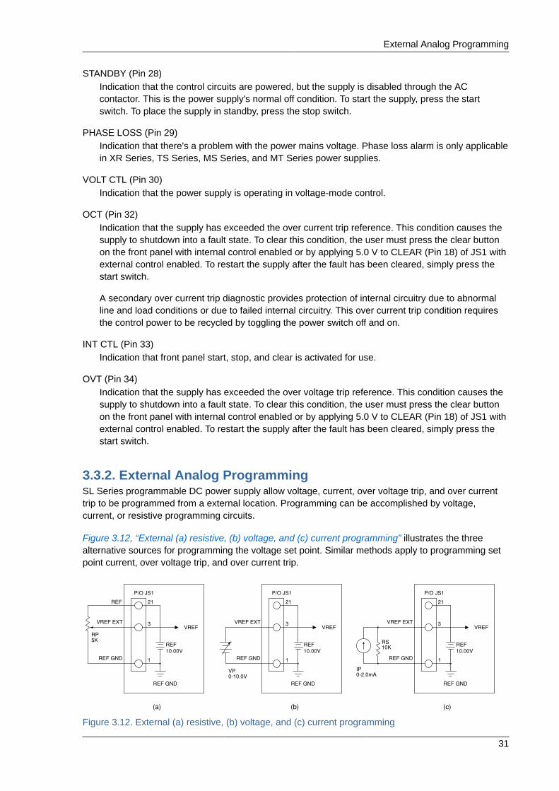
External Analog Programming
31
STANDBY (Pin 28)Indication that the control circuits are powered, but the supply is disabled through the ACcontactor. This is the power supply's normal off condition. To start the supply, press the startswitch. To place the supply in standby, press the stop switch.
PHASE LOSS (Pin 29)Indication that there's a problem with the power mains voltage. Phase loss alarm is only applicablein XR Series, TS Series, MS Series, and MT Series power supplies.
VOLT CTL (Pin 30)Indication that the power supply is operating in voltage-mode control.
OCT (Pin 32)Indication that the supply has exceeded the over current trip reference. This condition causes thesupply to shutdown into a fault state. To clear this condition, the user must press the clear buttonon the front panel with internal control enabled or by applying 5.0 V to CLEAR (Pin 18) of JS1 withexternal control enabled. To restart the supply after the fault has been cleared, simply press thestart switch.
A secondary over current trip diagnostic provides protection of internal circuitry due to abnormalline and load conditions or due to failed internal circuitry. This over current trip condition requiresthe control power to be recycled by toggling the power switch off and on.
INT CTL (Pin 33)Indication that front panel start, stop, and clear is activated for use.
OVT (Pin 34)Indication that the supply has exceeded the over voltage trip reference. This condition causes thesupply to shutdown into a fault state. To clear this condition, the user must press the clear buttonon the front panel with internal control enabled or by applying 5.0 V to CLEAR (Pin 18) of JS1 withexternal control enabled. To restart the supply after the fault has been cleared, simply press thestart switch.
3.3.2. External Analog ProgrammingSL Series programmable DC power supply allow voltage, current, over voltage trip, and over currenttrip to be programmed from a external location. Programming can be accomplished by voltage,current, or resistive programming circuits.
Figure 3.12, “External (a) resistive, (b) voltage, and (c) current programming” illustrates the threealternative sources for programming the voltage set point. Similar methods apply to programming setpoint current, over voltage trip, and over current trip.
1
P/O JS1
10.00VREF
REF GND
3
RP
21
(a) (b)
VP IP
10K
(c)
REF GND
REF
VREF EXTVREF VREF
VREF EXT
REF GND
21
3
REF GND
REF10.00V
P/O JS1
1 1
P/O JS1
10.00VREF
REF GND
3
21
REF GND
VREF EXTVREF
5K
0-10.0V 0-2.0mA
RS
Figure 3.12. External (a) resistive, (b) voltage, and (c) current programming

Chapter 3. Operation
32
Table 3.2. External Programming Parameters
Term Parm Description Input Range (V) Output Range
3 VREF EXT Voltage Set 0-10.0 0-100% FS Voltage
22 IREF EXT Current Set 0-10.0 0-100% FS Current
4 TVREF EXT Over Voltage Tip Set 0-10.0 0-110% FS Voltage
23 TIREF EXT Over Current Trip Set 0-10.0 0-110% FS Current
Note
If the applied analog input voltage exceeds 12.50 V, the PGL (program line) diagnostic LED alarmwill light and the power supply will enter into standby mode.
3.3.2.1. External Voltage Source ProgrammingFor programming using a voltage source, an external 10.0 V voltage source is placed between VREFEXT (Pin 3) and REF GND (Pin 1) of JS1 to control the output voltage.
The current set point, over voltage trip, and over current trip can be programmed in the same manner.Referring to the Section 3.3.1, “External 37-pin I/O Pin Definitions” for terminal identification, use IREFEXT (Pin 22) to program the current set point, TVREF EXT (Pin 4) to program over voltage trip, andTIREF EXT (Pin 23) to program over current trip. The power supply has been calibrated to producefull scale output voltage and current with 10.0 V inputs at the external reference input terminals.Furthermore, over voltage and over current trip have been calibrated to trip at 110% full scale outputvoltage and current with 10.0 V inputs at the external reference input terminals. Most commonly, IREFEXT (Pin 22), TVREF EXT (Pin 4), and TIREF EXT (Pin 23) are all jumpered together and tied to +10VREF (Pin 21).
3.3.2.2. External Current Source ProgrammingTo produce an external analog voltage reference to VREF EXT (Pin 3), a current source is applied toa shunt resistor. Using a 2 mA current source, place a 10.0 K precision metal film resistor betweenVREF EXT (Pin 3) and REF GND (Pin 1). The input impedance between terminals 1 and 3 is 10.0K and paralleling the additional resistor produces an equivalent resistance of 5 K. The 2 mA currentsource will produce 10.0 V at the external voltage reference input which will produce full scale outputvoltage.
The current set point, over voltage trip, and over current trip can be programmed in the same manner.Referring to the Section 3.3.1, “External 37-pin I/O Pin Definitions” for terminal identification, use IREFEXT (Pin 22) to program the current set point, TVREF EXT (Pin 4) to program over voltage trip, andTIREF EXT (Pin 23) to program over current trip. The power supply has been calibrated to producefull scale output voltage and current with 10.0 V inputs at the external reference input terminals.Furthermore, over voltage and over current trip have been calibrated to trip at 110% full scale outputvoltage and current with 10.0 V inputs at the external reference input terminals. Most commonly, IREFEXT (Pin 22), TVREF EXT (Pin 4), and TIREF EXT (Pin 23) are all jumpered together and tied to +10VREF (Pin 21).
3.3.2.3. External Resistive Source ProgrammingResistive programming requires connection of an external potentiometer or resistors between +10VREF (Pin 21), VREF EXT (Pin 3), and REF GND (Pin 1) of the JS1 connector. +10V REF (Pin 21)

External Analog Monitoring
33
is a 10.0V precision reference, REF GND (Pin 1) is the reference ground, and VREF EXT (Pin 3) isthe voltage set point input. Like front panel rotary control, the precision reference produces a voltageacross the potentiometer or resistors which is then used to produce the voltage set point. Metal filmresistors or a wire wound potentiometer will result in the lowest temperature coefficient.
The current set point, over voltage trip, and over current trip can be programmed in the same manner.Referring to the Section 3.3.1, “External 37-pin I/O Pin Definitions” for terminal identification, use IREFEXT (Pin 22) to program the current set point, TVREF EXT (Pin 4) to program over voltage trip, andTIREF EXT (Pin 23) to program over current trip. The power supply has been calibrated to producefull scale output voltage and current with 10.0 V inputs at the external reference input terminals.Furthermore, over voltage and over current trip have been calibrated to trip at 110% full scale outputvoltage and current with 10.0 V inputs at the external reference input terminals. Most commonly, IREFEXT (Pin 22), TVREF EXT (Pin 4), and TIREF EXT (Pin 23) are all jumpered together and tied to +10VREF (Pin 21).
3.3.3. External Analog MonitoringTwo outputs are provided for monitoring output voltage and current and for use in master/slave seriesand parallel operation. As illustrated in Figure 3.13, “Monitoring output (a) voltage and (b) current”,output monitoring voltage, VO2 (Pin 5), can be obtained by monitoring the voltage between terminalsVO2 (Pin 5) of JS1 and REF GND (Pin 1, Pin 2, or Pin 20) of JS1. Output monitoring current, IO2 (Pin24), can be obtained by monitoring the voltage between terminals IO2 (Pin 24) of JS1 and REF GND(Pin 1, Pin 2, or Pin 20) of JS1. Like the programming inputs, full scale output voltage and current willproduce 10.0 V. The output impedance of the analog moniotinr terminals is 100 Ω.
1,2,20
VO2
P/O JS1
5
VO=10V FSREF GND
24IO2
IO=10V FS
Figure 3.13. Monitoring output (a) voltage and (b) current
3.3.4. Digital Input LinesAll digital input lines are connected to the 37-pin JS1 connector located on the rear panel. Asillustrated in Figure 3.14, “Digital input control lines”, the digital input lines are START (Pin 17), STOP(Pin 19), CLEAR (Pin 18), and INTERLOCK SET (Pin 37). Functionally, the digital input control linesemulate the functions on the front panel when external control is enabled, indicated by the EXT CTLlight on the front panel. Enabling external control is described in Figure 3.6, “Enable or disable externalcontrol mode”. All digital input lines are triggered by a external momentary (pulsed) 5.0 V signal. IfSTOP (Pin 19) is left high, it will take presedence over the START (Pin 17) signal.

Chapter 3. Operation
34
TO SLAVES
37 INTERLOCK SET
19 STOP
START17
P/O JS1
26 +5
CLEAR18
Figure 3.14. Digital input control lines
Interlock set requires a either a physical short between 5.0 V (Pin 26) and INTERLOCK SET (Pin 37)of connector JS1 or application of a 5.0 V source with the positive connection at INTERLOCK SET(Pin 37) of JS1 and the negative connection at GND (Pin 7) of JS1. One of these two connectionsmust be made to enable operation of the power supply. If the interlock connection is broken then theLOC (interlock) fault LED lights, the power supply's internal AC contactor opens, and the unit stopsprocessing power. As illustrated, digital control lines may be paralleled with other supplies to allowsimultaneous control.
Note
Before the power supply will accept a reference voltage at INTERLOCK SET (Pin 37), interlockfunctionality must be enabled either from the front panel or from software. Refer to Figure 3.10,“Enable or disable external interlock functionality” for programming from the front panel.
3.3.5. Digital Output LinesAll digital output lines are connected to the 37-pin JS1 connector located on the rear panel.Functionally, the digital output lines provide the means to monitor diagnostic functions as functionalstatus. Figure 3.15, “Digital output contol lines” provides terminal identification for the various digitaloutput lines. Each output monitoring line can drive a 5.0 V, 5.0 mA load. An alarm condition willproduce a 5.0 V output at the respective terminal.
For a full explanation of all the available digital output lines, refer to Section 3.3.1, “External 37-pin I/OPin Definitions”.

Parallel and Series Operation
35
ALM13
33 INT CTL
EXT CTL14
OCT32
STANDBY28
THL9
PGL27
POWER8
OVT34
MONITORINGLINES
P/O JS1
30
11
VOLT CTL
CUR CTL
10
29
LOC
PHL
7 GND
STANDBY/ALM12
Figure 3.15. Digital output contol lines
Diagnostic functions include thermal overload, interlock, power, standby, phase loss, program line,over voltage, and over current. All diagnostic indicators have memory retention which saves the faultcondition until the power supply is reset. To clear a fault condition, the user must press the clear keyon the front panel with internal control or by applying 5.0 V to CLEAR (Pin 18) of JS1 with externalcontrol enabled. Alternatively, the supply can be cleared by turning the power supply off and on.
Diagnostic functions and control modes are embedded in the product's closed loop control. The powersupply will operate using voltage control or current control depending on which setting is lowest.Voltage control and current control also contain a soft start functionality which causes voltage and/or current to ramp to the desired set point after power is initiated. The soft start circuitry is reset uponpower-on or operation of any diagnostic function.
3.4. Parallel and Series Operation
3.4.1. Parallel OperationTwo or more SL Series power supplies can be connected in parallel to obtain a total output currentgreater than that available from one power supply. The total output current is the sum of the outputcurrents of the individual power supplies. Each power supply can be turned on or off separately.
3.4.1.1. Parallel Operation - DirectThe simplest parallel connection involves attaching the positive terminals of all supplies to beparalleled to the positive point of the load and attaching the negative terminals to the negative point ofthe load. The output current controls of each power supply can be separately set. The output voltagecontrol of one power supply (master) should be set to the desired output voltage; the other powersupply (slave) should be set for a slightly higher output voltage. The master will act as a constantvoltage source; the slave will act as a constant current source, dropping its output voltage to equal thatof the master.
Chapter 3. Operation
36
3.4.1.2. Parallel Operation - Master/SlaveMaster/slave parallel operation permits equal current sharing under all load conditions and allowscomplete control of output current from one master power supply.
Figure 3.16, “Master/Slave parallel connection” illustrates the terminal connection for master/slaveparallel operation and salient control circuitry. The control cable can be fabricated by the user orpurchased as an option, UID47, from the factory. These connections perform the following functions:
• Jumper connection between ISO (Pin 16) of the slave power supplies and ISI (Pin 35) of the masterpower supply connects the slave power supplies current monitoring outputs to the master powersupply current monitoring input. This connection allows the current of all slave power supplies to besummed along with that of the master power supply.
• Jumper connection between CONTROL (Pin 31) of the master and slave power supplies connectsthe control lines between the master and slave power supplies. Command of the control line isautomatically selected with the jumper connections.
• Jumper connection between REF GND (Pin 2), VREF EXT (Pin 3), IREF EXT (Pin 22) of the slavepower supplies to REF GND (Pin 2) of the master power supply enables control of the slave powersupplies from the master power supply.
• Jumper connection between POWER (Pin 8) of the master power supply to START (Pin 17) of theslave power supplies connects the power output digital control line of the master power supply to thestart digital control line of the slave power supplies. This connection causes slave units to turn onwhen the master unit is turned on.
• Jumper connection between STANDBY/ALM (Pin 12) of the master power supply and STOP (Pin19) of the slave power supplies connects the STANDBY/ALM digital control line of the master powersupply to the STOP digital control line of the slave power supplies. This connection causes theslaves units to turn off when the master unit is turned off or when a diagnostic condition appears.
• Jumper connections between TVREF EXT (Pin 4), +10V REF (Pin 21), and TIREF EXT (Pin 23) ofthe slave power supplies sets the slave voltage trip and over current trip set points just beyond fullscale values.
The slave power supply must be configured for external program (EXT PGM) input. The master unitcan configured for rotary, external program, or remote input. Configuration commands are discussed inSection 3.2.3, “Configuration Commands”.
To add a second slave unit, connect the output terminals of the second slave in parallel with the othertwo power supplies. Furthermore, connect a second control cable between the second slave unit andthe master unit.

Series Operation
37
P/O JS1
22
2
VO+
VO-LOAD
SLAVE
CURRENTMODE CONTROL
MASTERREF GND
VO-
VO+
IO2
2
24
P/O JS1
TO SECONDSLAVE
REF GND
IREF EXT
12STANDBY/ALM
POWER8
START
STOP19
17
21+10 REF
TVREF EXT4
23TIREF EXT
3VREF EXT
VO25
CONTROL31
CONTROL31
ISI35
16ISO
Figure 3.16. Master/Slave parallel connection
3.4.2. Series OperationTwo or more power supplies can be connected in series to obtain a total output voltage greater thanthat available from one power supply. The total output voltage is the sum of the output voltage of theindividual power supplies. Each power supply can be turned on or off separately.
Caution: No plus or minus voltage should exceed ±1000 Vdc. with respect to ground.
3.4.2.1. Series Opeation - DirectThe simplest series connection involves attaching the positive terminal of the first supply to thenegative terminal of the second supply. The load is connected between the negative terminal of thefirst supply and the positive terminal of the second supply. The output current controls of each powersupply are operative and the current limit is equal to the lowest control setting. If any one outputcurrent control is set too low with respect to the total output current, the series power supplies willautomatically crossover to constant current operation and the output voltage will drop.

Chapter 3. Operation
38
3.4.2.2. Seies Operation - Master/SlaveMaster/slave series operation permits equal voltage sharing under all load conditions and allowscomplete control of output voltage from one master power supply.
Figure 3.17, “Master/Slave series connection” illustrates the terminal connection for master/slaveseries operation and salient control circuitry. The control cable can be fabricated by the user orpurchased as an option, UID47, from the factory. These connections perform the following functions:
• Jumper connection between VO2 (Pin 5) of the master power supply and VREF EXT (Pin 3) of theslave power supplies connects the voltage monitoring voltage on the master power supply to theexternal voltage set point input on the slave power supplies. This makes the slave power suppliesoperate at the same voltage output as the master power supply.
• Jumper connection between POWER (Pin 8) of the master power supply to START (Pin 17) of theslave power supplies connects the power output digital control line of the master power supply to thestart digital control line of the slave power supplies. This connection causes slave units to turn onwhen the master unit is turned on.
• Jumper connection between STANDBY/ALM (Pin 12) of the master power supply and STOP (Pin19) of the slave power supplies connects the STANDBY/ALM digital control line of the master powersupply to the STOP digital control line of the slave power supplies. This connection causes theslaves units to turn off when the master unit is turned off or when a diagnostic condition appears.
• Jumper connections between TVREF EXT (Pin 4), +10V REF (Pin 21), IREF EXT (Pin 22), andTIREF EXT (Pin 23) of the slave power supplies sets the slave current control to maximum and setsthe voltage trip and over current trip set points just beyond full scale values.
The slave power supply must be configured for external program input. The master unit can configuredfor rotary, external program, or remote input. Configuration commands are discussed in Section 3.2.3,“Configuration Commands”.
To add a second slave unit, connect the output terminals of the second slave in series with the othertwo power supplies. Furthermore, connect a second control cable between the second slave unit andthe master unit.

Troubleshooting Guide
39
VREF EXT
REF GND
SLAVETO SECOND
P/O JS1
5
2
VO2
VO+
VO-
REF GNDMASTER
MODE CONTROLVOLTAGE
SLAVE
LOAD
VO-
VO+
2
3
P/O JS1
POWER
STANDBY/ALM
8
12
17
19STOP
START
IREF EXT22
TIREF EXT23
4TVREF EXT
21+10 REF
IO224
Figure 3.17. Master/Slave series connection
3.5. Troubleshooting GuideThe SL Series power supplies consist of a multistage power processing system. Because of itscomplexity, it is highly recommended that all repairs be performed by the factory or a qualified powersupply technician. Before attempting maintenance or repair, the technician should be familiar with thecomponents of the systems and the theory of operation. Some basic test equipment is also necessary:source of AC power, means of loading the power supply, DC voltmeter with accuracy and resolutionbetter than the programmable DC power supply specifications, and an oscilloscope.
Caution: When servicing the power supply, dangerous voltage levels exist. All AC andDC capacitors should be discharged. Be especially careful of person and equipmentwhen measuring primary circuitry since this is at line potential.
1. Fuse F1, F2, or F3 blows when the power supply is turned on. Power supply has a short on theprimary side.
• Check diode bridge DB1.
• Check for failed power semiconductor on the Chopper Module.
• Check for isolation to ground on the input side of the power supply.

Chapter 3. Operation
40
2. Over current trips and power supply cannot be reset. An auxiliary over current detector limits inputDC link current. Exceeding safe levels will cause an over current diagnostic condition that cannotbe reset.
• Restart the supply. Transient voltages on the input voltage could have caused the problem.
• Check diodes D1 through D4 on the secondary side of transformer T1.
• Check for a shorted winding on transformer T1.
• Check for failed IGBT's in the chopper and current fed inverter circuitry.
3. Unit goes to high output immediately after starting.
• Check for loose connectors internal to the power supply.
4. High ripple voltage.
• Check the mains voltage for balance and magnitude.
3.6. Calibration
3.6.1. Contol BoardThe control board contains digital potentiometers for fine adjustments of the reference and feedbackamplifiers. These potentiometers may be adjusted by using the front panel controls described inSection 3.2.4, “Calibration Commands”. These potentiometers can also be adjusted by using theCalibration Panel of the Remote Interface Software described in Section 4.5, “Calibration Panel”.
3.6.1.1. Reference Amplifier CalibrationConnect a voltmeter between terminal 6 of JS1 (positive) and terminal 1 of JS1 (negative). With onlythe control power applied, adjust potentiometer P5 for a 2.5006 V.
3.6.1.2. Voltage Feedback Amplifier CalibrationPlace a DC voltmeter across the output terminals of the power supply and place a second DCvoltmeter to monitor VO2, the voltage between terminal 5 of JS1 (positive) and terminal 1 of JS1(negative). Set the load to 50% rated output current at full scale voltage.
With only the control power applied, adjust potentiometer P2 for 0.000 V at VO2. Using the up/down(V/I DIS or TRIP DIS) keys or RS232 remote interface, set the output voltage to 50% full scale output.Turn on the power supply and adjust potentiometer P1 until the output voltage matches the set pointvoltage. Now set the output voltage to its full scale rating and measure the output voltage. Adjustpotentiometer P1 to equally divide the error between the half scale set point and the full scale point.
3.6.1.3. Current Feedback Amplifier calibrationPlace a DC ammeter in series with the load of the power supply and place a DC voltmeter to monitorIO2, the voltage between terminal 24 of JS1 (positive) and terminal 1 of JS1 (negative). Set the load to100% rated output current at 90% full scale voltage.
With only the control power applied, adjust potentiometer P4 for 0.000 V at IO2. Using the up/down(V/I DIS or TRIP DIS) keys or RS232 remote interface, set the output current to 50% full scale output.Turn on the power supply and adjust potentiometer P3 until the output current matches the set point

Driver Board
41
current. Now set the output current to its full scale rating and measure the output current. Adjustpotentiometer P3 to equally divide the error between the half scale set point and the full scale point.
3.6.2. Driver BoardThe driver board contains two potentiometers which are used to set under voltage and over currentprotection in the polyphase chopper circuitry. These potentiometer do not normally need adjustment inthe field.
3.6.2.1. Over Curent ProtectionOver current protection should only be calibrated after consultation with the factory.
Caution: Gross misadjustment can cause chopper and inverter failure.
Place a DC voltmeter between test point TP6 (positive) and test point TP7 (negative). With only thecontrol power applied, adjust potentiometer P1 to 6.00 V.
3.6.2.2. Under Voltage ProtectionUnder voltage protection should only be calibrated after consultation with the factory.
Caution: Gross misadjustment can cause chopper and inverter failure.
Connect the power supply to an adjustable AC source and connect an ac voltmeter to monitor thevoltage applied to the input terminals. Tests can be performed under no load conditions. Set the acsource to rated voltage. Turn the control power, press the start switch, and a adust the output voltageto 10% full scale output. Decrease the ac source to a value between 75% to 82% of rated voltage.Adjust potentiometer P2 until the output drops to zero; the transition will be abrupt.
Decrease the ac source to a value between 72% to 79% of rated voltage. The main contactor shouldturn off.

42

Chapter 4.
43
Remote Interface SoftwareThe Remote Interface Software is shipped with SL Series programmable DC power supplies. Thesoftware provides the user with a quick method to operate a Magna-Power Electronics power supplyunder computer control. The Remote Interface Software has six windows: the Virtual Control Panel,Command Panel, Register Panel, Calibration Panel, Firmware Panel, and Modulation Panel. TheVirtual Control Panel emulates the front panel of the SL Series programmable DC power supplies, theCommand panel programs and reads SCPI commands with user friendly buttons, the Register Panelprograms and reads registers, the Calibration Panel enables calibration of the digital potentiometers,the Firmware Panel enables the program stored internal to the power supply to be upgraded, and theModulation Panel eases programming of modulation parameters.
4.1. Application SetupTo communicate with the power supply, the front panel version, type of communication, address and/orport need to be specified. The options are:
1. Power supply series: Select the appropriate version corresponding to the power supply front paneltype.
2. Communications interface: RS232, RS485, IEEE-488 GPIB, LXI TCP/IP Ethernet, simulated, orothers depending on future developments. Figure 4.1, “RIS Panel Configuration Setup” displaysthe Applications Setup Window. Address requirements are:
• RS232: Port
• RS485: Address and port, 1-30
• IEEE-488: Address, 1-30
• Ethernet: Address and port
Figure 4.2, “LXI Communications Setup” illustrates the communications setup for LXI TCP/IPEthernet communications. The address specifies the desired device on the network to establishcommunications. To locate a particular device or to set a new address, press Find Device orChange Device's setting, respectively. The Find Devices panel displays all devices on the busthat are available for communications, as shown in Figure 4.3, “Find LXI TCP/IP Ethernet device”.The Change Device's Setting allows the address of the particular device to be changed. Whenchanging a device's address, the address in the Communication Setup will also change allowingcontinued communications. Similar panels are displayed for IEEE 488 GPIB, RS232, and RS485communications.
SIU850550361
Highlight
SIU850550361
Highlight

Chapter 4. Remote Interface Software
44
Figure 4.1. RIS Panel Configuration Setup
Figure 4.2. LXI Communications Setup
Figure 4.3. Find LXI TCP/IP Ethernet device

Virtual Control Panel
45
4.2. Virtual Control PanelFigure 4.4, “Virtual Control Panel” illustrates the Virtual Control Panel for the D Version front panelmodels. Other displays are available for the SL/XR front panel and the A Version front panel. TheVirtual Control Panel emulates front panel commands and provides the means to control the C Versionfront panel models.
Figure 4.4. Virtual Control Panel
4.3. Command PanelThe Command Panel is illustrated in Figure 4.5, “Command Panel”. The Command Panel is organizedinto three groups: commands and queries requiring data input, commands with only command syntax,and commands with only query syntax. The Output frame on the right of the window echoes theSCPI command used to communicate with the power supply. This feature provides the user with theproper syntax for each command. The Output frame can be cleared or saved to a file by pressingthe clear button or the save to file button. Commands in gray are not accessible with the particularconfiguration.

Chapter 4. Remote Interface Software
46
Figure 4.5. Command Panel
4.4. Register PanelThe Register Panel is illustrated in Figure 4.6, “Register Panel”. The Register Panel graphicallyrepresents the six internal registers of the power supply. Register functions, covered in the nextChapter, are briefly summarized below:
• Operation Register (oper): indicates the power supply's current operational state. The register isunlatched and is described in Section 5.1.9.1, “STAT:OPER:COND?”.
• Questionable Register (ques): indicates the current state of power supply alarms. The register isunlatched and is described in Section 5.1.9.2, “STAT:QUES:COND?”.
• Status Byte Register (STB): indicates communications error messages. The register is latched andis described in Section 5.3.3.6, “Read Status Byte Register”.
• Service Request Enable Register (SRE): a mask register for the STB. The register is described inSection 5.3.3.7, “Read and Set Service Request Enable Register”.
• Standard Event Status Register (ESR): a latched register which is similar to STB except it providesmore details. The register is described in Section 5.3.3.4, “Read Event Status Register”.
• Event Status Enable Register (ESE): mask register for the ESR. The register is described inSection 5.3.3.5, “Read and Set Event Status Enable Register”

Calibration Panel
47
Figure 4.6. Register Panel
As illustrated in the Register panel, each column denotes a register value, and the rows, markedby the leftmost column, are the bit positions. The get button at the column heading will acquire therespective register value for the power supply. The labels in each column indicate the meaning of eachbit. For example, bit 5 in the Ques column will light if fuse alarm is activated. The mask registers, SREand ESE, can be modified via the set button in their column heading. Enter the value in the "EnterValue in Selected Format" frame, and then press the set button. If no errors occur, then the new valuewill appear after the get button is pressed. The Results frame displays the returned register valuein decimal, hex and binary formats. The "Enter Value in Selected Format" frame allows the user tospecify the format for data entry.
The Output frame shows all communications with the power supply. The Output frame can be clearedor saved to a file by pressing the clear button or the save to file button.
4.5. Calibration PanelThe Calibration Panel, illustrated in Figure 4.7, “Calibration Panel”, provides easy access andprogrammability for the digital potentiometers. The Calibration Panel is password protected. Toenable changes, enter 1234 for the password and then press the adjacent set button. The fivedigital potentiometers can accept numbers from 0 to 255. Further commands include setting thepotentiometer to the factory default setting and end calibration procedure. The Output frame shows allcommunications with the power supply. The Output frame can be cleared or saved to a file by pressingthe clear button or the save to file button.
Voltage Scale and Current Scale are not available to the user. These are factory specific commandsthat require an alternate password to access.

Chapter 4. Remote Interface Software
48
Figure 4.7. Calibration Panel
4.6. Firmware PanelThe Firmware Panel is illustrated in Figure 4.8, “Firmware Panel”. The Firmware Panel enables theprogram stored internal to the power supply to be upgraded. The factory recommends that firmwareupgrades be performed only if there is an operational problem with the power supply.
The following steps list the procedure for upgrading the firmware:
• Turn the power supply off.
• Connect a RS232 cable between a serial port on a computer and connector JS3 on the powersupply.
• Press the select button and choose the file to be loaded.
• Press the start button. The Status frame will display "Initiating."
• Turn on the power supply. If the supply is not turned on within 10 seconds, "Time Out" will bedisplayed in the Status frame indicating communications is lost.
During the process of upgrading the firmware, the front panel of the power supply will remain blank.After communications is established, the Status frame will initially display "Erasing" and the CurrentAddress frame will display the address in memory being erased. After the entire memory is erased, theStatus frame will display "Loading " and the Current Address frame will display the address in memorybeing loaded. The Status frame will display "Finished" and the front panel display will return to normalafter the memory is reprogrammed.
Pressing the stop button will terminate execution at any time.

Modulation Panel
49
Figure 4.8. Firmware Panel
4.7. Modulation PanelThe Modulation Panel is illustrated in Figure 4.9, “Modulation Panel”. The Modulation Panel enables auser to set and view the modulation settings as described in Section 5.1.6, “Modulation Commands”.The modulation settings consist of control input, modulation type (multiplication or addition), table row,modulation voltage input, and modulation factor. The Modulation Panel provides the form to programa linear or piece-wise linear lookup table for the selected modulation type. The lookup table can havea maximum of 50 data points. The modulation voltage input, VMOD, must be entered in ascendingorder. For lookup tables with less than 50 data points, VMOD must be terminated with a Mod value of9999. Any data entered for modulation factor on the terminating row is ignored. The Output frame onthe right of the window displays all of the communications with the power supply. The Output framecan be cleared or saved to a file by pressing the clear button or the save to file button. More detailsabout the modulation functionality's principle of operation are available in Section 5.1.6, “ModulationCommands”

Chapter 4. Remote Interface Software
50
Figure 4.9. Modulation Panel
Chapter 5.
51
Computer ProgrammingThere is a versatile range of methods and interfaces that can be used to program the SL Seriesprogrammable DC power supply from a computer or programmable logic controller. StandardCommands for Programmable Instrumentation (SCPI) are provided for basic ASCII interfacingwithout any necessary drivers; these commands are documented in Section 5.1, “SCPI Commands”.In addition, an IVI-COM Driver is included with the installation CD and is available for downloadfrom the Magna-Power Electronics web page for more advanced programming requirements. Thedriver allows the power supply to communicate through many different programming languages andsoftware environments, namely: Visual C++, Visual C#, Visual Basic .NET, Visual Basic 6.0, LabVIEW,LabWindows/CVI, MATLAB, Measure Foundry, and Agilent VEE Pro. Refer to Section 5.7, “IVI-COMDriver” for further details.
SL Series products purchased with optional LXI TCP/IP Ethernet (+LXI) or IEEE-488 GPIB (+GPIB)interfaces have additional commands and programming instructions, detailed in Section 5.4, “LXI TCP/IP Ethernet Communications” and Section 5.3, “IEEE-488 GPIB Communications”, respectively.
5.1. SCPI CommandsStandard Commands for Programmable Instrumentation (SCPI) are provided for Magna-PowerElectronics products. These commands provide programming compatability with other instruments.SCPI commands are ASCII textual strings, which are sent to the instrument over the physical layer.Commands are a series of one or more keywords—many of which take parameters. The subsectionsprovide more details on all the supported commands. For commands related to optional IEEE-488GPIB interface and LXI TCP/IP Ethernet interface refer to Section 5.3.3, “IEEE-488 GPIB SCPICommands and Registers” and Section 5.4.3, “LXI TCP/IP Ethernet SCPI Commands”, respectively.
The following syntax is used in this manual.
SCPI SyntaxSquare Brackets [ ]
Items within the square brackets are optional. Brackets plus their contents can be omitted whenthe command is issued.
Angle Brackets < >Items within the angle brackets, indicating a specific data type, provide parameter descriptions.See Section 5.1.1, “Parameter Data Types” for more information.
5.1.1. Parameter Data TypesTable 5.1. SCPI Parameter Data Types
Symbol Data Type Example(s)
<> Null, no data.
<NR1> Digits with an implied decimal point assumed at the right of theleast-significant digit.
-326326
<NR2> Digits with an explicit decimal point. -32.63.26
<NR3> Digits with an explicit decimal point and an exponent. 3.26E+2326.0E-2
<NRf> Extended format that includes <NR1>, <NR2> and <NR3>. 326-326.03.26E2

Chapter 5. Computer Programming
52
Symbol Data Type Example(s)
<NRf+> Expanded decimal format that includes <NRf>, MIN, and MAX,where MIN and MAX are the minimim and maximum limit valuesin the range specification for the parameter.
326-326.03.26E2MAX
<bool> Boolean data, can be numeric (0, 1) or name (OFF, ON). 1ON
<string> String program data, enclosed in either single or double quotes. Magna-PowerElectronics
5.1.2. Restricted SCPI Command SetCommands and queries described in Section 5.1, “SCPI Commands” require the power supply to beconfigured for REMOTE operation. There are instances, however, when the power supply may beconfigured for ROTARY or EXT PGM and use of certain SCPI command from a computer interfacefeatures may be desirable. As defined in Table 5.2, “Restricted SCPI command set available while inROTARY or EXT PGM configuration”, a reduced set of commands and queries are available duringthese modes of operation, enabling allowing for computer communications at all times.
Table 5.2. Restricted SCPI command set available while in ROTARY or EXT PGM configuration
SL Panel SLC Panel
Command Type Command/Query Example Command Query Command Query
CAL:IDN • •
CAL:PASS
CAL:POT • •
CAL:SCAL:VOLT • •
CAL:SCAL:CURR • •
CAL:SCAL:INP • •
CAL:DEF
Calibration
CAL:STOP
CONT:INT • • • •
CONT:EXT • • • •
REM:SENS • • • •
INTE • • • •
Configuration
CONF:SETPT • • • •
MEAS:VOLT? • •Measure
MEAS:CURR? • •
MOD:TYPE:SEL • • • •
MOD:TABL • • • •
MOD:SAVE • •Modulation
MOD:TABL:LOAD • •
OUTP? • •
OUTP:ARMOutput
OUTP:START • •

Restricted SCPI Command Set
53
SL Panel SLC Panel
Command Type Command/Query Example Command Query Command Query
OUTP:STOP • •
OUTP:PROT:CLE • •
VOLT AND VOLT:TRIG • •
VOLT:PROT • • • •
CURR AND CURR:TRIG • •Source
CURR:PROT • • • •
STAT:OPER:COND? • •Status
STAT:QUES:COND? • •
SYST:VERS? • •System
SYST:ERR? • •
TRIG
INIT • •Trigger
ABORt
NET:VERS? • •
NET:MAC? • •
NET:SER? • •
NET:ADDR • • • •
NET:GATE • • • •
NET:SUBN • • • •
NET:PORT • • • •
NET:HOST • • • •
LXI EthernetTCP/IPCommunications
NET:DHCP • • • •
GPIB:VERS? • •
GPIB:ADDR • • • •
*CLS • •
*ESR? • •
*ESE • • • •
*STB? • •
*SRE? • • • •
*IDN? • •
*SAV
*RCL
IEEE-488 GPIBCommunications
*RST

Chapter 5. Computer Programming
54
5.1.3. Calibration Commands
5.1.3.1. CAL:IDN Description
This command updates the power supply’s identification string for the power supply model. TheCAL:IDN string can have up to 100 characters. Before this command can be used, a passwordmust be validated by CAL:PASS. Typically, this command is for Magna-Power Electronics useonly.
Command SyntaxCALibrate:IDN <string>
ParametersCompany Name, Power Supply Model, Serial Number
ExamplesCAL:IDN Magna-Power Electronics Inc., TSD16-900, S/N: 1161-5225
Query SyntaxCAL:IDN?
Returned Parameter<string>
Related Commands*IDN
5.1.3.2. CAL:PASS Description
This command protects against system calibration corruption and initiates the calibrationsequence.
Command SyntaxCAL:PASS <NR1>
ExamplesCALIBRATE:PASSWORD 1234CAL:PASS 1234
5.1.3.3. CAL:POT Description
This command sets the value for the specified potentiometer. The variable specifies thepotentiometer to be adjusted, 1 thru 5, and the second variable specifies the potentiometer setting,0 through 255.
Command SyntaxCALibrate:POT <NR1>,<NR2>
ExamplesCALIBRATE:POT 1,123CAL:POT 5,11

Calibration Commands
55
Query SyntaxCALibrate:POT?
Returned Parameter<NR1>
5.1.3.4. CAL:SCAL:VOLT Description
This command sets the voltage scale factor for the power supply.
Command SyntaxCALibrate:SCALe:VOLTage <NRf>
ExamplesCALIBRATE:SCALE:VOLTAGE 16.0CAL:SCAL:VOLT 16.0
Query SyntaxCALibrate:SCALe:VOLTage?
Returned Parameter<NR3>
5.1.3.5. CAL:SCAL:CURR Description
This command sets the current scale factor for the power supply.
Command SyntaxCALibrate:SCALe:CURRent<NRf>
ExamplesCALIBRATE:SCALE:CURRENT 900.0CAL:SCAL:CURR 900.0
Query SyntaxCALibrate:SCALe:CURRent?
Returned Parameter<NR3>
5.1.3.6. CAL:SCAL:INP Description
This command sets the full scale external programming inputs for voltage, current, over voltagetrip, and over current trip. The scaling factor for the programming inputs must match the scalingfactor set with hardware on the control board.
Command SyntaxCALibrate:SCALe:INPut<NRf>
ExamplesCALIBRATE:SCALE:INPUT 10.0CAL:SCAL:INP 10.0

Chapter 5. Computer Programming
56
Query SyntaxCALibrate:SCALe:INPut?
Returned Parameter<NR3>
5.1.3.7. CAL:DEF Description
This command sets the Calibration potentiometers to the factory defaults.
Command SyntaxCALibrate:DEFaults
ExamplesCALibrate:DEFaultsCAL:DEF
5.1.3.8. CAL:STOP Description
This command terminates the calibration subsystem.
Command SyntaxCALibrate:STOP
ExamplesCALibrate:STOPCAL:STOP
5.1.4. Configuration Commands
5.1.4.1. CONT:INT Description
This command enables or disables the front panel switches and keys for start, stop, arm, andclear.
The query command, CONT:INT?, returns the status of internal control.
Command Syntax[CONFigure]:CONTrol:INTernal <bool>
Parameters0 | OFF1 | ON
ExamplesCONF:CONT:INT ONCONT:INT 0
Query Syntax[CONFigure]:CONTrol:INTernal?

Configuration Commands
57
Returned Parameter0 | 1
5.1.4.2. CONT:EXT Description
This command enables or disables the external inputs for start, stop, arm, and clear.
The query command, CONT:EXT?, returns the status of external control.
Command Syntax[CONFigure]:CONTrol:EXTernal <bool>
Parameters0 | OFF1 | ON
ExamplesCONF:CONT:EXT ONCONT:EXT 0
Query Syntax[CONFigure]:CONTrol:EXTernal?
Returned Parameter0 | 1
5.1.4.3. REM:SENS Description
This command sets voltage sensing to remote or local mode. Remote sensing, as described inSection 2.4.1, “Remote Voltage Sensing”, improves the degradation of regulation which will occurat the load when the voltage drop in the connecting wires is appreciable. The local sense modemonitors the voltage at the output terminals of the power supply.
The query command, REM:SENS?, returns the state of the sense lines.
Command Syntax[CONFigure]:REMote:SENSe <bool>
Parameters0 | OFF1 | ON
ExamplesCONF:REM:SENS ONREMOTE:SENSE 0
Query Syntax[CONFigure]:REMote:SENSe?
Returned Parameter0 | 1

Chapter 5. Computer Programming
58
5.1.4.4. INTE Description
This command enables or disables the external interlock feature. Interlock, described inSection 3.3.4, “Digital Input Lines”, is used for applications where the power supply needs to bedisabled under external conditions.
The query command, INTE?, returns the status of external interlock.
Command Syntax[CONFigure]:INTErlock
Parameters0 | OFF1 | ON
ExamplesCONF:INTE ONINTE 0
Query Syntax[CONFigure]:INTErlock?
Returned Parameter0 | 1
5.1.4.5. CONF:SETPT Description
This command sets the operational mode of the power supply: ROTARY, KEYPAD, EXT PGM, orREMOTE. Keypad configuration is available for TS Series, MS Series, and MT Series supplieswith the D-Version front panel.
The query command, CONF:SETPT?, returns the operation mode of the power supply.
Command Syntax[CONFigure]:SETPT <NR1>
Parameters0 | ROTARY1 | KEYPAD2 | EXT PGM3 | REMOTE
ExamplesCONF:SETPT 0SETPT 0
Query Syntax[CONFigure]:SETPT?
Returned Parameter<NR1>

Measure Commands
59
5.1.5. Measure Commands
5.1.5.1. MEAS:VOLT? Query Syntax
MEASure:VOLTage[:DC]?
ExamplesMEAS:VOLT?MEASURE:VOLTAGE:DC?
Returned Parameter<NR2>
5.1.5.2. MEAS:CURR? Query Syntax
MEASure:CURRent[:DC]?
ExamplesMEAS:CURR?MEASURE:CURRENT:DC?
Returned Parameter<NR2>
5.1.6. Modulation CommandsThe Modulation Subsystem, available on SL Series, XR Series, and TS Series, MS Series, and MTSeries units with the D Version front panel, adjusts the output voltage or current according to thevoltage measured on the external analog input, pin 25 of JS1, named VMOD. This signal has anallowed input range 0-10 V. Modulation requires the power supply to be configured for remote mode.Rotary control mode or external program control mode cannot be used with these commands.
Modulation allows a set point adjustment of voltage or current by another input. The modulationsignals can be derived from an external device, such as a thermistor, or from the sampling of theoutput current or voltage. When used with software containing advanced numerical methods, feedingthe output voltage or current to adjust the set point current or voltage allows user defined outputprofiles. The system, incorporating this feature, introduces another negative feedback path with gaincontrolled by a user programmed attenuator.
Modulation can be introduced into the control loop either adding a variable to the set point or bymultiplying a variable with the set point. Additive functions are useful for introducing series and parallelimpedances and multiplier functions are useful for adjusting voltages or currents sources. Table 5.3,“Modulation Function Subsystem Parameters” describes the four options: control input 1 and 2 forvoltage and current control and control type 0 and 1 for multiplier and additive functions.
5.1.6.1. MOD:TYPE:SELThis command is composed of two comma separated, modulation parameters. The first parameter,control input, defines whether the modulation table adjusts output voltage or output current. When thecontrol input is set to 1, VMOD selects the modulation table to adjust output voltage. When controlinput is set to 2, VMOD selects the modulation table to adjust output current. Setting the control inputto the default value of 0, disables the modulation function. Information on programming the lookuptable is provided in Table 5.4, “Modulation Table Parameters”.

Chapter 5. Computer Programming
60
The second command parameter, control type, defines the expression for modulating output voltageor current. With type set to 0, table data points are used in a multiplying expression. With type set to 1,table data points are used in an addition expression.
The choice of using type 0 or type 1 modulation depends on the application. Only one set point canbe modulated at any given time. The query command returns two comma separated parameters, thecontrol input followed by the control type.
Table 5.3. Modulation Function Subsystem Parameters
Control Input Control Type
0 1
(Default) 0 Disabled Disabled
1 Vo=Gv[Vref×Mod(VMOD)] Vo=Gv[Vref+Mod(VMOD)]
2 Io=Gi[Iref×Mod(VMOD)] Io=Gi[Iref+Mod(VMOD)]
Notes:
1. Vo is the adjusted output voltage as a function of the modulation operator
2. Io is the adjusted output current as a function of the modulation operator
3. Vref is input voltage set point reference
4. Iref is input current set point reference
5. VMOD is the input modulation set point reference
6. Gv is the system gain as define by the full scale output voltage, Vfs, divided by the maximum inputvoltage set point reference, Vref,max
7. Gi is the system gain as define by the full scale output current, Ifs, divided by the maximum inputcurrent set point reference, Iref,max
Mod(VMOD), modulation, can be an expression, constant, or other numerical operator. A user friendlymethod chosen by Magna-Power Electronics is a table based algorithm using piecewise linearapproximation. This numerical method allows linear or non-linear modulation to be introduced simplybe defining the constants in a table.
Command SyntaxMODulation:TYPE:SELect <NR1>[,<NR1>]
ExamplesMOD:TYPE:SEL 1,0MOD:TYPE:SEL 2,1MODulation:TYPE:SELect 0
Query SyntaxMODulation:TYPE:SELect?
Returned Parameter<NR1>, <NR1>
5.1.6.2. MOD:TABLThis command programs the user defined modulation table described in Section 5.1.6.1, “MOD:TYPE:SEL ”. The feature allows the user to program non-linear output voltage and current

Modulation Commands
61
profiles to fit their application needs, such as source emulation or output adjustments with respectto an external sensor. Modulation functionality may be used either by issuing SCPI commands asdetailed in this section or by entering the values into a table from the RIS Panel software as detailed inSection 4.7, “Modulation Panel”
The lookup table contains 4 columns and up to 50 rows; it stores an output profile as a function of theanalog input voltage applied to terminal 25 of JS1, VMOD. As shown in Table 5.4, “Modulation TableParameters”, the first column stores the table row and the second column sets an analog input VMOD.The third column store the Mod value associated with VMOD for that table row.
The fourth column of the lookup table, Loc, defines whether the table is stored in an active ortemporary location. Certain applications may need to transition between different tables while thepower supply is still running. For example, emulation of solar panel’s voltage/current characteristicsrequires continuous external data acquisition along with quick and smooth table loading . Themodulation subsystem provides two storage locations, Loc 0 or 1, to help improve table loadingperformance. With Loc set to 0, data will be stored to the Active Table, the table which is activelyapplied to the modulation function. With Loc set to 1, data will be stored to the Cache Table, the tableintended to be accessed in the next in the profile. During the power on cycle, modulation tables storedin EPROM are copied into volatile RAM.
Modulation linearly interpolates between data points to form a piecewise-linear curve. Each columnhas to have data in an acceptable range. All tables less than 50 rows must be terminated with aVMOD value of 9999. Mod values at and past a row with VMOD of 9999 does not affect modulation.
Table 5.4. Modulation Table Parameters
Column
1 2 3 4
Description Row VMOD Mod Loc
Acceptable Range 1 to 50 0.0 to 10.0 -1000.0 to 1000.0 0 to 1
While the table will store any value within the acceptable range, the power supply is limitedby its output voltage and current specifications. For example, when using type 1 modulation,MOD:TYPE:SEL 1,1, a user can store a Mod value of -1000, but the power supply will only output avoltage down to 0 V. From row 1 to 50, VMOD has to be in ascending order.
Modulation points are read with two comma separated parameters, formatted as: Row, Loc. The querywill return four parameters, formatted in the same way as the save table command above.
Command SyntaxMOD:TABL <NR1>(<NRF>,<NRF>,<NR1>)
ExamplesMOD:TABL 12(0.13, 1.6, 1)MODulation:TABLe 20(2.0, 15.002, 0)MOD:TABL 13(1.5, -1.29, 0)MOD:TABL 14(9999, 0, 1)
Query SyntaxMOD:TABL? <NR1>,<NR1>
Returned Parameter<NR1>(<NRF>,<NRF>,<NR1>)

Chapter 5. Computer Programming
62
5.1.6.3. MOD:SAVEThis command copies the Active Table in RAM to a non-volatile, EEPROM memory. The Active Table,which is stored in RAM, loses its data on power down cycles. This command allows this data to berecovered at the power on cycle.
Command SyntaxMOD:SAVEMODulation:TABLe:SAVE
ExamplesMOD:SAVE
Related CommandsMOD:TABL:LOAD
5.1.6.4. MOD:TABL:LOADThis command copies all data stored in the Cache Table to the Active Table. The command providestwo optional parameters for initiating the activate set points for voltage and current. The command letsusers quickly load tables and simultaneous change the power supply’s output operating point.
Command SyntaxMOD:TABL:LOAD [<NRF>, <NRF>]
ExamplesMOD:TABL:LOADMODulation:TABLe:LOADMODulation:TABL:LOAD 93.4, 30.3
Related CommandsMOD:SAVE
5.1.7. Output Commands
5.1.7.1. OUTP? Description
This query returns the output state of the power supply. A 1 indicates the power supply isenergized and a 0 indicates the power supply is off.
Query SyntaxOUTPut[:STATe]?
ExamplesOUTP?
Returned Parameter0 | 1
Related Commands*RST, *RCL, *SAV
Output Commands
63
5.1.7.2. OUTP:ARM Description
This command selects between the modes of operation. There are two modes of operation forthe power supply: normal mode and auto sequence mode. Normal mode energizes the currentparameters of the supply until stopped. Auto sequence mode sequentially steps through thememory updating the supply’s parameters as it increments. Each memory location contains thevoltage set point, current set point, over voltage trip, over current trip, and period. The periodparameter specifies the time period for operating at the memory location when auto sequenceoperation is deployed. When enabled, the ARM light lights on the front panel.
To initiate a program sequence, select the starting memory location, execute this command, andissue an OUPT:START (see OUTP:START) or use the front panel start switch. The ARM light willblink after the start command. If this process reaches the upper memory limit, memory location99, the following memory location will revert back to 0 and continue. Auto sequence operationwill continue until an OUTP:STOP is commanded or a memory location with period set to 0 isencountered.
ARM? returns the arm state of the power supply unit.
Command SyntaxOUTP:ARM <bool>
Parameters0 | OFF1 | ON
ExamplesOUTP:ARM OFFOUTP:ARM 1
Query SyntaxOUTP:ARM
Returned Parameter0 | 1
Related Commands*RST, OUTP:START, OUTP:STOP
5.1.7.3. OUTP:START Description
This command closes the power supply’s input contactor and initiates either normal or autosequence mode. Auto sequence mode will be initiated if the ARM option is enabled. Normal modeenergizes the power supply with the current parameters for voltage set point, current set point,over voltage trip, and over current trip. Auto sequence mode will sequentially step through memorylocations until the stop is commanded, OUTP:STOP, or a terminating condition is reached (seePER, OUTP:STOP).
Command SyntaxOUTP:START
ExamplesOUTP:STARTOUTPUT:START
Chapter 5. Computer Programming
64
Related Commands*RST, OUTP:STOP, OUTP:ARM, PER
5.1.7.4. OUTP:STOP Description
This command opens the power supply’s input contactor and initiates either normal or autosequence mode.
Command SyntaxOUTP:STOP
ExamplesOUTP:STOPOUTPUT:STOP
Related Commands*RST, OUTP:START, OUTP:ARM, PER
5.1.7.5. OUTP:PROT:CLE Description
This command clears the alarm latches. There are seven alarm latches, namely: interlock,program line, phase balance, thermal, over voltage trip, over current trip, and input. When a faultis detected, the power supply is rendered to an alarm state. The power supply cannot be restarteduntil the protection condition is cleared and the latch is reset.
Command SyntaxOUTPut:PROTection:CLEar
ExamplesOUTP:PROT:CLEOUTPUT:PROTECTION:CLEAR
Related Commands*RST, *RCL, *SAV
5.1.8. Source Commands
5.1.8.1. VOLT and VOLT:TRIG Description
These commands set the power supply's immediate voltage level or the pending triggered voltagelevel. The immediate level is the voltage programmed for the immediate power supply output.The pending triggered level is a stored voltage value that is transferred to the power supplywhen a trigger occurs. A pending triggered level is unaffected by subsequent VOLT commandsand remains in effect until the trigger subsystem receives a trigger or is aborted with an ABORtcommand. In order for VOLT:TRIG to be executed, the trigger subsystem must be initiated (seeINIT).
VOLT? and VOLT:TRIG? return presently programmed immediate and triggered voltage levels. Ifno triggered level is programmed, then the voltage level is returned for both values. VOLT? MAXand VOLT? MIN return the maximum and minimum programmable immediate voltage levels.
Source Commands
65
VOLT:TRIG? MAX and VOLT:TRIG? MIN return the maximum and minimum programmabletriggered voltage levels.
Command Syntax[SOURce]:VOLTage[:LEVel][:IMMediate][:AMPLitude] <NRf+>[SOURce]:VOLTage[:LEVel]:TRIGgered[:AMPLitude] <NRf+>
ExamplesVOLT 200VOLTAGE:LEVEL 200VOLTAGE:LEVEL:IMMEDIATE:AMPLITUDE 2.5VOLT:TRIG MAXVOLTAGE:LEVEL:TRIGGERED 20
Query Syntax[SOURce]:VOLTage[:LEVel][:IMMediate][:AMPLitude]?[SOURce]:VOLTage[:LEVel][:IMMediate][:AMPLitude]? MAX[SOURce]:VOLTage[:LEVel][:IMMediate][:AMPLitude]? MIN[SOURce]:VOLTage[:LEVel]:TRIGgered[:AMPLitude]?[SOURce]:VOLTage[:LEVel]:TRIGgered[:AMPLitude]?[SOURce]:VOLTage[:LEVel]:TRIGgered[:AMPLitude]? MAX[SOURce]:VOLTage[:LEVel]:TRIGgered[:AMPLitude]? MIN
Returned Parameter<NR2>
Related Commands for VOLT*SAV, *RCL, *RST
Related Commands for VOLT:TRIGABOR, VOLT, *RST
5.1.8.2. VOLT:PROT Description
This command sets the over voltage trip (OVT) level of the power supply. If the output voltageexceeds the OVT level, then the power supply output is disabled and the Questionable Conditionstatus register OV bit is set (see Table 5.6, “Bit Configuration of the Questionable Register”). Anover voltage trip condition can be cleared with the OUTP:PROT:CLE command after the conditionthat caused the OVT trip is removed.
VOLT:PROT? returns presently programmed OVT level. VOLT:PROT? MAX and VOLT:PROT?MINreturn the maximum and minimum programmable OVT levels.
Command Syntax[SOURce]:VOLTage:PROTection[:LEVel] <NRf+>
ExamplesVOLT:PROT 21.5VOLTAGE:PROTECTION:LEVEL 145E-1
Query Syntax[SOURce]:VOLTage:PROTection[:LEVel]?[SOURce]:VOLTage:PROTection[:LEVel]? MIN[SOURce]:VOLTage:PROTection[:LEVel]? MAX

Chapter 5. Computer Programming
66
Returned Parameter<NR2>
Related CommandsOUTP:PROT:CLE, *RST, *SAV, *RCL
5.1.8.3. CURR and CURR:TRIG Description
These commands set the immediate current level or the pending triggered current level of thepower supply. The immediate level is the current programmed for the power supply output. Thepending triggered level is a stored current value that is transferred to the power supply outputwhen a trigger occurs. A pending triggered level is unaffected by subsequent CURR commandsand remains in effect until the trigger subsystem receives a trigger or is aborted with an ABORtcommand. In order for CURR:TRIG to be executed, the trigger subsystem must be initiated (seeINITiate )
CURR? and CURR:TRIG? return presently programmed immediate and triggered levels. If notriggered level is programmed, then the CURR level is returned for both values. CURR? MAXand CURR? MIN return the maximum and minimum programmable immediate current levels.CURR:TRIG? MAX and CURR:TRIG? MIN return the maximum and minimum programmabletriggered current levels.
Command Syntax[SOURce]:CURRent[:LEVel][:IMMediate][:AMPLitude] <NRf+>[SOURce]:CURRent[:LEVel]:TRIGgered [:AMPLitude] <NRf+>
ExamplesCURR 200CURRENT:LEVEL MINCURRENT:LEVEL:IMMEDIATE:AMPLITUDE 2.5CURR:TRIG 20CURRENT:LEVEL:TRIGGERED 20
Query Syntax[SOURce]:CURRent[:LEVel][:IMMediate][:AMPLitude]?[SOURce]:CURRent[:LEVel][:IMMediate][:AMPLitude]? MAX[SOURce]:CURRent[:LEVel][:IMMediate][:AMPLitude]? MIN[SOURce]:CURRent[:LEVel]:TRIGgered[:AMPLitude]?[SOURce]:CURRent[:LEVel]:TRIGgered[:AMPLitude]? MAX[SOURce]:CURRent[:LEVel]:TRIGgered[:AMPLitude]? MIN
Returned Parameter<NR2>
Related Commands*SAV, *RCL, *RST
Related CommandsABOR, CURR, *RST
Source Commands
67
5.1.8.4. CURR:PROT Description
This command sets the over current trip (OCT) level of the power supply. If the output currentexceeds the OCT level, then the power supply output is disabled and the Questionable Conditionstatus register OC bit is set (see Table 5.6, “Bit Configuration of the Questionable Register”). Anover current trip condition can be cleared with the OUTP:PROT:CLE command after the conditionthat caused the OCT trip is removed.
CURR:PROT? returns presently programmed OCT level. CURR:PROT? MAX and CURR:PROT?MIN return the maximum and minimum programmable OCT levels.
Command Syntax[SOURce]:CURRage:PROTection[:LEVel] <NRf+>
ExamplesCURR:PROT MAX CURRENT:PROTECTION:LEVEL 145E-1
Query Syntax[SOURce]:CURRent:PROTection[:LEVel]?[SOURce]:CURRent:PROTection[:LEVel]? MIN[SOURce]:CURRent:PROTection[:LEVel]? MAX
Returned Parameter<NR2>
Related CommandsOUTP:PROT:CLE, *RST, *SAV, *RCL
5.1.8.5. PER Description
This command is available on TS Series, MS Series, and MT Series programmable DC powersupplies with the D Version front panel. This command sets the period of time that the powersupply will remain in the state during auto sequence operation. The minimum unit for theperiod command is 10 msec and the maximum unit is 9997 sec. There are 3 reserved numbersassociated with this command, namely: 0, 9998 and 9999. When a 0 is detected in auto sequenceoperation, the power supply will stop as if a stop command condition (see OUTP:STOP)occurred.When a 9998 is detected, the following memory location will be zero. When 9999 is detected,the power supply will operate at that memory state indefinitely or until stop (see OUTP:STOP)is commanded. The period’s duration can be overridden by using the start command (seeOUTP:START) to advance the memory to the next state or the stop command (see OUTP:STOP) tostop the power supply.
Command Syntax[SOURce]:PERiod <NRf+>
ExamplesSOUR:PER 200SOURCE:PERIOD 1345SOUR:PER MAX
Query Syntax[SOURCE]:PERiod?[SOURCE]:PERiod? MIN[SOURCE]:PERiod? MAX

Chapter 5. Computer Programming
68
Returned Parameter<NR1>
Related Commands*RST, OUTP:START, OUTP:STOP, OUTP:ARM
5.1.8.6. REC:MEM Description
The recall command sets the current memory location of the power supply. In remote mode, 100(0 - 99) memory locations are available for programming. In local mode, the 10 (0 - 9) memorylocations are available for programming.
Command Syntax[RECall]:MEMory <NR1>
ExamplesREC:MEM 10MEM 99
Query SyntaxRECall:MEMory?
Returned Parameter<NR1>
Related Commands*RCL, *SAV
5.1.9. Status Commands
5.1.9.1. STAT:OPER:COND? Description
This query returns the value of the Operation Register which is a read-only register that holds thereal-time (unlatched) condition of the operational status of the power supply. The bit configurationof the Operation Register is shown in Table 5.5, “Bit Configuration of the Operation Register”.
Query SyntaxSTATus:OPERation:CONDition?
ExamplesSTAT:OPER:COND?STATUS:OPERATION:CONDITION?
Returned Parameter<NR1> (Register value)
Table 5.5. Bit Configuration of the Operation Register
Bit Weight Abbreviation Description
0 1 ARM Arm
1 2 SS Soft Start
2 4 LOCK Locked

Status Commands
69
Bit Weight Abbreviation Description
3 8 INT Internal Control
4 16 EXT External Control
5 32 WTG Interface is Waiting for Trigger
6 64 STBY Standby
7 128 PWR Power
8 256 CV Constant Voltage
9 512 RSEN Remote Sense
10 1024 CC Constant Current
11 2048 STBY/ALM Standby or Alarm
12-15 NU Not Used
5.1.9.2. STAT:QUES:COND? Description
This query returns the value of the Questionable Register. The Questionable Register is a read-only register that holds the real-time (unlatched) condition of the questionable status of thepower supply. The bit configuration of the Questionable Register is shown in the Table 5.6, “BitConfiguration of the Questionable Register”.
Query SyntaxSTATus:QUEStionable:CONDition?
ExamplesSTAT:QUES:COND?STATUS:QUESTIONABLE:CONDITION?SOUR:PER MAX
Returned Parameter<NR1> (Register value)
Table 5.6. Bit Configuration of the Questionable Register
Bit Weight Abbreviation Description
0 1 OV Over Voltage Tripped
1 2 OC Over Current Tripped
2 4 PB Phase Balance Protection Tripped
3 8 PGM Program Line Protection Tripped
4 16 OT Over Temperature Protection Tripped
5 32 FUSE Fuse Protection Tripped
6 64 NU Not Used
7 128 ALM Alarm Protection Tripped
8 256 ILOC Interlock
9 512 REM Remote
10-15 NU Not Used

Chapter 5. Computer Programming
70
5.1.10. System Commands
5.1.10.1. SYST:VERS? Description
The SYST:VERS? query returns the firmware and hardware version of the power supply. Thereturned value has the form Firmware Rev. X.X, Hardware Rev. X.X.
Query SyntaxSYSTem:VERSion?
ExamplesSYST:VERS?SYSTEM:VERSION?
Returned Parameter<Firmware Rev. XX.Y, Hardware Rev. XX.Y>
5.1.10.2. SYST:ERR? Description
The SYST:ERR? query returns the error messages that have occurred in the system. The formatof the return string is an error number followed by corresponding error message string. The errorsare stored in a FIFO (first-in, first-out) buffer. As the errors are read, they are removed from thequeue. When all errors have been read, the query returns 0, "NO ERROR." If more errors haveaccumulated than the queue can hold, the last error in the queue will be -350, "Queue Overflow."When system errors occur, the Standard Event Status Register (ESR), records the error groups asdefined in Table 5.7, “Standard Event Status Register Error Bits”. Table 5.8, “Error Messages” listssystem errors that are associated with SCPI syntax errors and with interface problems.
Table 5.7. Standard Event Status Register Error Bits
Bit Error Code Error Type
5 100 through -199 Command
4 200 through -299 Execution
3 300 through -399 Device dependent
2 400 through -499 Query
Table 5.8. Error Messages
Error Error String Error Description
-100 Command error Generic command error
-102 Syntax error Unrecognized command or data type
-108 Parameter not allowed Too many parameters
-222 Data out of range E.g., outside the range of this device
-350 Queue overflow Errors lost due to too many errors inqueue
-400 Query error Generic query error
Query SyntaxSYSTem:ERRor?

Trigger Commands
71
ExamplesSYST:ERR?SYSTEM:ERROR?
Returned Parameter<error number>, <error string>
5.1.11. Trigger Commands
5.1.11.1. TRIG Description
This command controls remote triggering of the power supply. When the trigger subsystemis enabled, a TRIG command generates a trigger signal. The trigger signal will then initiate apending level change as specified by CURR[:LEV]:TRIG or VOLT[:LEV]:TRIG. Afterwards, theOperation Register will be cleared. If INIT:CONT is on, the trigger subsystem is immediately re-enabled for subsequent triggers. As soon as it is cleared, the WTG bit is again set to 1.
Command SyntaxTRIGger[IMMediate]
ExamplesTRIGTRIGGER:IMMEDIATE
Related CommandsABOR, CURR:TRIG, INIT, *TRG, VOLT:TRIG
5.1.11.2. INIT Description
This command enables the trigger system. When the initiate command is enabled, a TRIGcommand allows specified triggering action to occur. If the initiate subsystem is not enabled, alltrigger commands are ignored. If INIT:CONT is OFF, then INIT enables the trigger subsystemonly for a single trigger action; INIT must then be repeated prior to further trigger commands. IfINIT:CONT is ON, then the trigger subsystem is continuously enabled.
INIT:CONT? returns the state of the continuous trigger mode.
Command SyntaxINITiate[:IMMediate]INITiate:CONTinuous <bool>
Parameters for INIT[:IMM]:None
Parameters for INIT:CONT:0 | OFF1 | ON
ExamplesINITINITIATE:IMMEDIATEINIT:CONT 1

Chapter 5. Computer Programming
72
INITIATE:CONTINUOUS OFF
Query Syntax for INIT[:IMM]:None
Query Syntax for INIT:CONT:INIT:CONT?
Returned Parameter0 | 1
Related CommandsABOR, *RST, TRIG
5.1.11.3. ABORt Description
This command cancels any trigger actions presently in process. Any pending trigger levels arereset to their immediate values. ABORt also resets the WTG bit in the Operation Register. If initiatecontinuous is enabled (INIT:CONT ON), the trigger subsystem immediately re-initiates itselfafter ABORt, thereby setting WTG. ABOR is executed at power turn on and upon execution of *RCLor *RST.
Command SyntaxABORt
ExamplesABOR
Related CommandsINIT, TRIG, *RCL, *RST
5.2. RS232 CommunicationsAll Magna-Power Electronics products come standard with RS232 communications, which providesthe simpliest means to communicate with the power supply. The RS232 configuration settings aredetailed in Table 5.9, “RS232 Interface Configuration”. The RS232 terminal, connector JS3, is detailedin Table 5.10, “RS232 Terminal Definition, Connector JS3”. All the commands detailed in Section 5.1,“SCPI Commands” are supported over RS232.
Note
When using external converters that utilize the RS232 port, the settings from Table 5.9, “RS232Interface Configuration” must be used or the product will not communicate.
Table 5.9. RS232 Interface Configuration
Parameter Value
Baud Rate 19200
Data Size 8-bit
Parity None
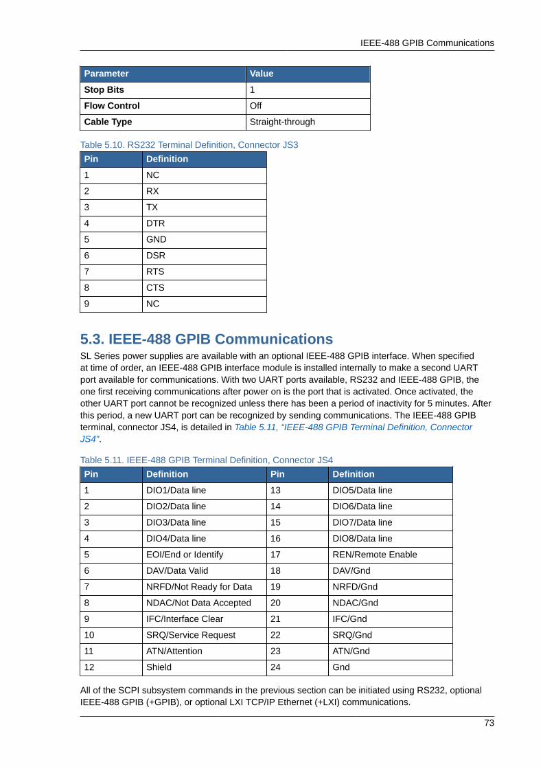
IEEE-488 GPIB Communications
73
Parameter Value
Stop Bits 1
Flow Control Off
Cable Type Straight-through
Table 5.10. RS232 Terminal Definition, Connector JS3
Pin Definition
1 NC
2 RX
3 TX
4 DTR
5 GND
6 DSR
7 RTS
8 CTS
9 NC
5.3. IEEE-488 GPIB CommunicationsSL Series power supplies are available with an optional IEEE-488 GPIB interface. When specifiedat time of order, an IEEE-488 GPIB interface module is installed internally to make a second UARTport available for communications. With two UART ports available, RS232 and IEEE-488 GPIB, theone first receiving communications after power on is the port that is activated. Once activated, theother UART port cannot be recognized unless there has been a period of inactivity for 5 minutes. Afterthis period, a new UART port can be recognized by sending communications. The IEEE-488 GPIBterminal, connector JS4, is detailed in Table 5.11, “IEEE-488 GPIB Terminal Definition, ConnectorJS4”.
Table 5.11. IEEE-488 GPIB Terminal Definition, Connector JS4
Pin Definition Pin Definition
1 DIO1/Data line 13 DIO5/Data line
2 DIO2/Data line 14 DIO6/Data line
3 DIO3/Data line 15 DIO7/Data line
4 DIO4/Data line 16 DIO8/Data line
5 EOI/End or Identify 17 REN/Remote Enable
6 DAV/Data Valid 18 DAV/Gnd
7 NRFD/Not Ready for Data 19 NRFD/Gnd
8 NDAC/Not Data Accepted 20 NDAC/Gnd
9 IFC/Interface Clear 21 IFC/Gnd
10 SRQ/Service Request 22 SRQ/Gnd
11 ATN/Attention 23 ATN/Gnd
12 Shield 24 Gnd
All of the SCPI subsystem commands in the previous section can be initiated using RS232, optionalIEEE-488 GPIB (+GPIB), or optional LXI TCP/IP Ethernet (+LXI) communications.

Chapter 5. Computer Programming
74
The IEEE-488 standard defines a method for status reporting. As illustrated in figure 4.1, the methoduses the IEEE-488.1 Status Byte (STB). Three bits of this byte are defined as: Master StatusSummary (MSS) Bit, Event Status Bit (ESB), and Message Available (MAV) Bit.
The Master Status Summary (MSS) is an unlatched bit. When the Status Byte Register is read using aStatus Byte Register query, bit 6 will be 1 if there are any conditions requiring service.
The STB is masked by the Service Request Enable Register (SRE) to allow the user to mask specificor all events from setting the MSS bit to 1. The MSS bit is obtained by logical OR’ing the bits of theenabled Status Byte Register.
The Event Status Bit (ESB) is set when one of the events defined in the Event Status Register (ESR)Table 5.12, “Event Status Register” has occurred. Like the STB, the ESR is masked by the EventStatus Enable Register (ESE) to allow the user to mask specific or all events from setting the ESB to1.
The Message AVailable (MAV) bit is set to 1 when a message is available in the output buffer.
5.3.1. IEEE-488 GPIB Communication using the Remote InterfaceSoftwareChapter 4, Remote Interface Software describes application of the Remote Interface Software whichis shipped with SL Series power supplies. This software provides the user with a quick method tooperate a Magna-Power Electronics power supply under computer control. The software can beconfigured for a number of communication interfaces; IEEE-488 GPIB is included as one of theseinterfaces.
To use the Remote Interface Software with optional IEEE-488 GPIB communications, the address,1 to 30, defined in the Remote Interface Software and the address encoded in the power supplymust match. Address 0 is assigned to the GPIB master. The default programmable DC power supplyaddress is 1, but if the address is unknown, press Find Device in the Communication Setup menu.The routine scans all the devices on the bus providing their addresses and identifications. Select thedesired device and press OK; this automatically changes the address in the Communication Setup.The same result can be achieved with a double click on the desired device. After communications isestablished, the address of the device may be changed by pressing Change Device's Settings.
5.3.2. IEEE-488 GPIB Communications with MAXNational Instruments offers Measurement and Automation Explorer (MAX), a Graphical User Interface,as a terminal emulation program for configuring an Interchangeable Virtual Instrument (IVI). MAX isusually installed with one of National Instrument's Application Development Environments such asLabVIEW, Measurement Studio, or with hardware product drivers such as NI-488 and NI-DAQ.
To operate the power supply with MAX, the instrument must first be located for communications. Thefollowing steps describe this procedure.
1. Run the MAX application program.
2. In the Configuration window, press the + sign to the left of Devices and Interfaces to view theinstalled devices.
3. If there is more than one IEEE-488 GPIB device listed, then select the correct GPIB device.
4. Press Scan for Instruments on the menu bar and wait several seconds.
5. At least one instrument should appear under the GPIB controller. If no instruments appear, thenrefer to Section 5.3, “IEEE-488 GPIB Communications” to verify the correct setup.
IEEE-488 GPIB SCPI Commands and Registers
75
6. On the menu bar, press Communicate with Instrument. The NI-488 Communicator dialog boxshould appear.
7. In the NI-488 Communicator dialog box, press the Configure EOS button. The Termination Methoddialog box should appear.
• Select the option Send EOI at end of Write.
• Enter 0 into th EOS byte.
• Press OK.
5.3.3. IEEE-488 GPIB SCPI Commands and Registers
5.3.3.1. GPIB:VERS? Description
This query is available only for units with the IEEE-488 GPIB (+GPIB) option installed. This queryreads the firmware version of the GPIB communication module.
Query Syntax[SYSTem][:COMMunicate]:GPIB:VERSion?
ExamplesSYST:COMM:GPIB:VERS?GPIB:VERS?
Returned Parameter<Firmware Ver. XX.Y>
5.3.3.2. GPIB:ADDR Description
This command is available only for units with the IEEE-488 GPIB (+GPIB) option installed. Thiscommand sets the address of the GPIB module of the power supply. The address can be 1 to 30where address 0 is normally assigned to the GPIB Master. The factory default address is 1.
Command Syntax[SYSTem][:COMMunicate]:GPIB:ADDRess <NR1>
Parameters1 - 30
ExamplesSYST:COMM:GPIB:ADDR 27GPIB:ADDR 27
Query Syntax[SYSTem][:COMMunicate]:GPIB:ADDR?
Returned Parameter<NR1>
Chapter 5. Computer Programming
76
5.3.3.3. Clear Description
This command clears all status register (ESR, STB and error queue).
Command Syntax*CLS <>
Related Commands*RST
5.3.3.4. Read Event Status Register Description
This query reads the Event Status Register (ESR). After reading the ESR, the register is cleared.The bit configuration of the ESR is the same as the Event Status Enable Register (*ESE). Thereturn parameter is weighted as shown in Table 5.12, “Event Status Register”.
The Power On Bit (PON) is set every time the power supply is reset. It can be used to detect apower outage or power supply reset.
Query Syntax*ESR?
Example*ESR?
Return Parameter<NR1> (Register value)
Related Commands*CLS, *ESE, *ESE?
Table 5.12. Event Status Register
Bit Weight Abbreviation Description
0 1 OPC Operation Complete
1 2 NU Not Used
2 4 QYE Query Error
3 8 DDE Device Dependent Error
4 16 EXE Execution Error
5 32 CME Command Error
6 64 NU Not Used
7 128 PON Power On Event, 1 after power on
5.3.3.5. Read and Set Event Status Enable Register Description
This command programs the Event Status Enable Register (ESE). The programming determineswhich events of the Event Status Register (ESR) set the Event Status Bit (ESB) of the Status ByteRegister (STB). A "1" in the bit position enables the corresponding event. All of the enabled eventsof the ESE are logically OR’d to cause the ESB of the STB to be set.

IEEE-488 GPIB SCPI Commands and Registers
77
Command Syntax*ESE <NR1>
Example*ESE 255
Query Syntax*ESE?
Return Parameter<NR1>
Related Commands*ESR?, *STB?
5.3.3.6. Read Status Byte Register Description
This query reads the Status Byte Register (STB), defined in Table 5.13, “Status Byte Register”,which contains the Master Status Summary (MSS) bit, Event Status (ESB) bit, and the MessageAvailable (MAV) bit. Unlike reading ESR, the STB is not cleared after it is read. The MAV bit iscleared at power on or by *CLS.
Query Syntax*STB?
Example*STB?
Return Parameter<NR1> (Register value)
Related Commands*ESR?, *ESE
Table 5.13. Status Byte Register
Bit Weight Abbreviation Description
0 1 NU Not Used
1 2 NU Not Used
2 4 NU Not Used
3 8 NU Not Used
4 16 MAV Message Available
5 32 ESB Event Status Bit
6 64 NU Not Used
7 128 NU Not Used
5.3.3.7. Read and Set Service Request Enable Register Description
This command sets the Service Request Enable Register (SRE). This register, defined inTable 5.14, “Service Request Enable Register”, determines which bits from the Status ByteRegister (see *STB for its bit configuration) are allowed to set the Master Status Summary (MSS)

Chapter 5. Computer Programming
78
Bit. A 1 in any SRE bit position enables the corresponding Status Byte Register bit. All Status ByteRegister enabled bits are then logically OR’d and placed in bit 6 of the Status Byte Register. When*SRE is cleared (by programming it with 0), the power supply cannot generate a service request tothe controller.
Command Syntax*SRE <NR1>
Example*SRE 20
Query Syntax*SRE?
Return Parameter<NR1> (Register value)
Related Commands*ESR, *ESE
Table 5.14. Service Request Enable Register
Bit Weight Abbreviation Description
0 1 NU Not Used
1 2 NU Not Used
2 4 NU Not Used
3 8 NU Not Used
4 16 MAV Message Available
5 32 ESB Event Status Bit
6 64 MSS Master Summary
7 128 NU Not Used
5.3.3.8. Read Model Number, Part Number, and Serial Number Description
This query requests the power supply to identify itself. It returns a string composed of three fieldsseparated by commas
Query Syntax*IDN?
Return ParameterCompany Name, Power Supply Model, S/N (string format)
ExampleMagna-Power Electronics Inc., XR16-375, S/N: 1162-0361, F/W:1.0
Related CommandsCALibrate:IDN

IEEE-488 GPIB SCPI Commands and Registers
79
5.3.3.9. Save Description
This command is available for all SL Series, XR Series, and TS Series, MS Series, and MT Seriesunits with the D Version front panel. This command stores the present state of the power supplyat the specified location in memory. Data can be saved in 100 memory locations. The followingpower supply parameters are stored by *SAV:
VOLT[:LEV][:IMM]CURR[:LEV][:IMM]VOLT:PROT[:LEV]CURR:PROT[:LEV]PER
Command Syntax*SAV <NR1>
Parameters0 - 99
Example*SAV 1
Related Commands*RCL, MEM
5.3.3.10. Recall Description
This command restores the power supply to a state that was previously stored in memory locationwith a *SAV command. The *RCL command can recall data in 100 memory locations. For SLSeries programmable DC power supply, only memory location 0 is available. The followingparameters are recalled:
VOLT[:LEV][:IMM]CURR[:LEV][:IMM]VOLT:PROT[:LEV]CURR:PROT[:LEV]PER
The *RCL command forces an ABORt command before resetting any parameters. ABOR cancelsany trigger actions presently in progress and sets INIT:CONT to OFF.
At power turn-on, recall is commanded at the memory location prior to turn-off state.
Command Syntax*RCL <NR1>
Parameters0 - 99
Example*RCL 1
Related Commands*RST, *SAV

Chapter 5. Computer Programming
80
5.3.3.11. Reset Description
This command resets the power supply to factory default states as defined below:
OUTP[:STAT] OFFCURR[:LEV][:IMM] 0CURR[:LEV]:TRIG 0VOLT[:LEV][:IMM] 0VOLT[:LEV]:TRIG 0PER 0INIT:CONT OFFVOLT:PROT[:LEV] 110% of MAXCURR:PROT[:LEV] 110% of MAX
*RST also forces an ABORt command.
Command Syntax*RST <>
5.4. LXI TCP/IP Ethernet CommunicationsSL Series power supplies are available with an optional LXI TCP/IP Ethernet interface. The optionalLXI TCP/IP Ethernet interface meets the LXI Class C, Revision 1.2 standard. When specified attime of order, an Ethernet interface module is installed to make a second UART port availablefor communications. With two UART ports available, RS232 and Ethernet, the one first receivingcommunications after power on is the port that is activated. Once activated, the other UART portcannot be recognized unless there has been a period of inactivity for 5 minutes. After this period, anew UART port can be recognized by sending communications. By default, DHCP is enabled on thepower supply. In the absence of a DHCP server, the power supply will default to the settings definedin Table 5.15, “Default LXI TCP/IP Ethernet settings (without DHCP Server)”. The LXI TCP/IP Ethernetinterface, connector JS5, is detailed in Table 5.16, “LXI TCP/IP Ethernet Terminal Definition, JS5”
Table 5.15. Default LXI TCP/IP Ethernet settings (without DHCP Server)
Parameter Value
IP Address 169.254.###.###
Subnet Mask 255.255.0.0
Default Gateway 0.0.0.0
DNS Server 0.0.0.0
MAC Address 01:1E:6F:##:##:##
Table 5.16. LXI TCP/IP Ethernet Terminal Definition, JS5
Pin Definition
1 TX+
2 TX-
3 RX+
4 NC
5 NC
6 RX-
7 NC

Connectivity and IP Address Negotiation
81
Pin Definition
8 NC
Ethernet communications can be made though the Remote Interface Software, a terminal emulationprograms like Microsoft Windows (tm) HyperTerminal Program, 3rd party software, or through acomputer’s web page browser. In the latter case, software, programmed into the LXI TCP/IP Ethernetinterface module, allows the power supply to be recognized and to communicate directly with thecomputer without the need for additional programs stored in the computer.
An IVI-COM Driver is included with the installation CD and is available for download from theMagna-Power Electronics’ web page. The driver allows the power supply to communicate throughmany different programming languages. The driver handles the low-level bus protocols simplifyingautomation development. It supports TCP/IP, GPIB, and RS232 using standard VISA resourcedescriptors. For additional documentation and details on using the IVI-COM driver, see Section 5.7,“IVI-COM Driver”.
5.4.1. Connectivity and IP Address NegotiationWhen the LXI TCP/IP Ethernet module is configured for DHCP, but the DHCP server cannot belocated, the module falls back to an Auto-IP configuration. The device then automatically selects anIP address from 169.254.###.### subnet as described in RFC 3927 (Request for Comments 3927- Dynamic Configuration of IPv4 Link-Local Addresses). This routine is the same as that used withoperating systems such as Microsoft Windows. This allows the user to use the LXI TCP/IP Ethernetinterface in the absence of a DHCP server.
The LAN status LED, located at the rear of the power supply, provides LAN fault and deviceidentification as defined as follows:
• On – Normal Operation. The device has a properly configured IP address and the network cable isconnected.
• Flashing – Device Identify. The LXI Device Identification function was enabled via the InstrumentIdentification web page. This identification can help the user to quickly locate the unit and distinguishit from similar devices.
• Off – LAN Fault. The device is experiencing one or more of the following LAN fault conditions: failureto acquire a valid IP address, detection of a duplicate IP address on the network, failure to renew analready acquired DHCP lease, or the LAN cable is disconnected.
The LAN Reset button provides a way to reset the LAN configuration password and to set the deviceback to DHCP/Auto-IP mode. To activate the LAN Reset function, ensure the power supply is on andin standby mode. Hold down the LAN Reset button for approximately 4 seconds. Observe that theLAN LED rapidly flashes and after 4 seconds, release the LAN Reset button. The LAN configurationpassword will be reset to blank and the module will be set to DHCP/Auto-IP enabled.
The MAC address consists of two number groups, in format: ##:##:##:##:##:##. For Magna-Power Electronics products, the first three bytes are always 01:1E:6F. The second threebytes are determined by the the LXI TCP/IP Ethernet interface's serial number, convertedto hex. This serial number can be queried from the power supply using the SCPI commandSYSTem:COMMunicate:NETwork:SERial.
The LXI TCP/IP Ethernet module supports the VXI-11 discovery protocol allowing the device to bediscovered on the network by software such as National Instruments Measurement and AutomationExplorer, Agilent Connection Expert, or the Remote Interface Software supplied with the power supply.
Chapter 5. Computer Programming
82
5.4.2. LXI TCP/IP Ethernet Control and Discovery MethodsThe Ethernet module supports the VXI-11 discovery protocol allowing the device to be discovered onthe network by software such as National Instruments' Measurement and Automation Explorer, AgilentConnection Expert, or the Remote Interface Software supplied with the power supply.
5.4.2.1. Remote Interface SoftwareChapter 4, Remote Interface Software describes application and configuration of the Remote InterfaceSoftware which is shipped with SL Series programmable DC power supply. This software providesthe user with a quick method to operate a Magna-Power Electronics’ power supply under computercontrol. The software can be configured for a number of communication interfaces; Ethernet isincluded as one of these interfaces.
To use the Remote Interface Software with optional Ethernet communications, the address parametersin the Remote Interface Software and that encoded in the power supply must match. The factorydefault for DHCP is 1 (on) allowing the IP address to be automatically set by the DHCP server onthe network. If DHCP is off and the address is unknown, the device can be located using the RemoteInterface Software supplied with the power supply. To access discovery, press Find Device in theCommunication Setup menu. The routine scans all the devices on the network and provides theiraddresses and identifications. Select the desired device and press OK; this automatically changesthe address in the Communication Setup. The same result can be achieved with a double click on thedesired device. After communications is established, the address of the device may be changed bypressing Change Device’s Settings.
5.4.2.2. Web BrowserThe LXI TCP/IP Ethernet interface has an embedded web server that allows the user to view andchange the module's network settings and provides basic control of the power supply. Magna-PowerElectronics LXI TCP/IP Ethernet interface is LXI Class C compliant under LXI Standard Revision 1.2.
To access the web server, first determine the module's IP address via one of the discovery methodsdescribed in Section 5.4.2.1, “Remote Interface Software”. Alternatively, if the host computer supportsNetBIOS over TCP/IP, you may use the device's NetBIOS name instead of the IP address.
Open a WC3 compliant web browser such as Microsoft Internet Explorer, Firefox, or Opera to http://[ipaddress]/ or http://[name]/. The instrument information screen will be displayed as shown inFigure 5.1, “Web interface information panel”. This figure provides the basic information about theconfiguration and allows the user to enable or disable the LXI Identification. Click Enable Identify orDisable Identify to change the state of the LXI Identification. When LXI Identification is enabled, theLAN LED on the back of the power supply unit will blink. This can help the user to quickly locate thepower supply and distinguish it from similar devices.
To change the Ethernet interface's network settings, click the Configure tab in the upper right. Thebrowser will prompt for a username and password if you have not authenticated the device already.To authenticate, enter admin for the username and leave the password field blank. The instrumentconfiguration screen, Figure 5.2, “Web interface configure panel”, will appear. This page enables theuser to change the Hostname (which corresponds to the NetBIOS name), the description, password,and TCP/IP configuration. After changes to the configuration are made, click the Save Config button.The configuration will be saved, the Ethernet interface will reboot and instructions will be displayed forreconnecting to the interface.
Web control of the power supply requires Adobe Flash Player which is available for download fromhttp://get.adobe.com/flashplayer/. To control the power supply, click the Control tab in the upper right.The browser may prompt for a username and password if you have not authenticated the device
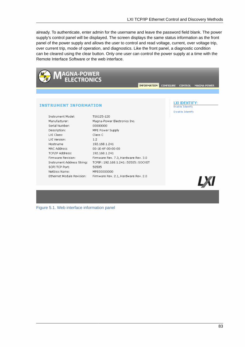
LXI TCP/IP Ethernet Control and Discovery Methods
83
already. To authenticate, enter admin for the username and leave the password field blank. The powersupply’s control panel will be displayed. The screen displays the same status information as the frontpanel of the power supply and allows the user to control and read voltage, current, over voltage trip,over current trip, mode of operation, and diagnostics. Like the front panel, a diagnostic conditioncan be cleared using the clear button. Only one user can control the power supply at a time with theRemote Interface Software or the web interface.
Figure 5.1. Web interface information panel

Chapter 5. Computer Programming
84
Figure 5.2. Web interface configure panel

LXI TCP/IP Ethernet Control and Discovery Methods
85
Figure 5.3. Web interface control panel
5.4.2.3. Discovery using NI Measurement and Automation ExplorerTo access discovery with NI Measurement and Automation Explorer, the NI-VISA add-on modulemust be installed along with the standard software package. Start NI Measurement and AutomationExplorer, right-click on Devices and Interfaces, and then select "Create New…" Select "VISA TCP/IP Resource" from the list. Click Next and then select Auto-detect of LAN Instrument. Click Next andthe software will scan the local network for VXI devices and display them for configuration for furtherusage with NI-VISA and related software.
5.4.2.4. Discovery using Agilent Connection ExpertTo access discovery with Agilent Connection Expert, start Agilent Connection Expert. Select yourcomputer's LAN interface and then click the Add Instrument button at the top of the screen. Thesoftware will scan the local network for VXI devices and display them for configuration for further usewith Agilent VISA compatible software.
5.4.2.5. HyperTerminalThe following procedure outlines using Microsoft Windows (tm) HyperTerminal Program tocommunicate using the LXI TCP/IP Ethernet communications.
1. Start the HyperTerminal application and when prompted select "TCP/IP (Winsock)" in the "Connectusing" list box.

Chapter 5. Computer Programming
86
2. Insert the recorded IP address in the "Host address" text box and port number in the "Portnumber" text box.
3. Click the "OK" button.
4. Set the following properties for HyperTerminal's ASCII setup:
• Send line ends with line feeds.
• Echo typed characters locally.
• Append line feeds to incoming line ends.
5. Type "*IDN?" in the input window and press enter. The identification of the instrument shouldappear.
5.4.3. LXI TCP/IP Ethernet SCPI Commands
5.4.3.1. NET:VERS? Description
This query reads the firmware and hardware versions of the Ethernet communications module.
Query Syntax[SYSTem][:COMMunicate]:NETwork:VERSion?
ExamplesSYST:COMM:NET:VERS?NET:VERS?
Returned Parameter<Firmware Ver. XX.Y, Hardware Rev. XX.Y>
5.4.3.2. NET:MAC? Description
This query returns the MAC address of the Ethernet module. MAC address consist of two numbergroups: the first three bytes are known as the Organizationally Unique Identifier (OUI), which isdistributed by the IEEE, and the last three bytes are the device’s unique serial number. The sixbytes are separated by hyphens. The MAC address is unique to the instrument and cannot bealtered by the user.
Query Syntax[SYSTem][:COMMunicate]:NETwork:MAC?
ExamplesSYST:COMM:NET:MAC?NET:MAC?
Returned Parameter<XX-XX-XX-YY-YY-YY>
Related CommandsNET:ADDR, NET:GATE, NET:SUBN, NET:PORT, NET:HOST, NET:DHCP

LXI TCP/IP Ethernet SCPI Commands
87
5.4.3.3. NET:SER? Description
This command sets the serial number of the Ethernet module. The serial number is an integerranging from 1 to 16777215 and cannot be altered by the user.
Query Syntax[SYSTem][:COMMunicate]:NETwork:SER?
ExamplesSYST:COMM:NET:SER?NET:SER?
Returned Parameter<NR1>
5.4.3.4. NET:ADDR Description
This command sets the static address of the Ethernet module of the power supply. The factorydefault address setting is 192.168.1.100.
Command Syntax[SYSTem][:COMMunicate]:NETwork:ADDRess <string>
ParametersIP address is represented with 4 bytes each having a range of 0-255 separated by periods
ExamplesSYSTem:COMM:NET:ADDR 192.168.10.2NET:ADDR 192.168.10.2
Query Syntax[SYSTem][:COMMunicate]:NETwork:ADDRess?
Returned Parameter<string>
Related CommandsNET:MAC, NET:GATE, NET:SUBN, NET:PORT, NET:HOST, NET:DHCP
5.4.3.5. NET:GATE Description
This command sets the Gateway IP address of the Ethernet module of the power supply. Thefactory default Gateway IP setting is 192.168.1.1.
Command Syntax[SYSTem][:COMMunicate]:NETwork:GATE <string>
ParametersGateway IP address is represented with 4 bytes each having a range of 0-255 separated by dots
ExamplesSYSTem:COMM:NET:GATE 192.168.10.2NET:GATE 192.168.10.2

Chapter 5. Computer Programming
88
Query Syntax[SYSTem][:COMMunicate]:NETwork:GATE?
Returned Parameter<string>
Related CommandsNET:MAC, NET: ADDR, NET:SUBN, NET:PORT, NET:HOST, NET:DHCP
5.4.3.6. NET:SUBN Description
This command sets the subnet IP Mask address of the Ethernet module of the power supply. Thefactory subnet mask setting is 255.255.255.0.
Command Syntax[SYSTem][:COMMunicate]:NETwork:SUBNet <string>
ParametersIP mask address is represented with 4 bytes each having a range of 0-255 separated by periods.
ExamplesSYSTem:COMM:NET:SUBNet 255.255.255.128NET: SUBNet 255.255.255.128
Query Syntax[SYSTem][:COMMunicate]:NETwork:SUBNet?
Returned Parameter<string>
Related CommandsNET:MAC, NET: ADDR, NET:GATE, NET:PORT, NET:HOST, NET:DHCP
5.4.3.7. NET:PORT Description
This command sets the Socket (Port) of the Ethernet module of the power supply. The factorydefault port setting is 50505. The factory recommends port values greater than 49151 to avoidconflicts with registered Ethernet port functions.
Command Syntax[SYSTem][:COMMunicate]:NETwork:PORT <NR1>
Parameters16-bit socket number (1 to 65,535)
ExamplesSYSTem:COMM:NET: PORT 50505NET: PORT 50505
Query Syntax[SYSTem][:COMMunicate]:NETwork:PORT?
Returned Parameter<NR1>

USB Communications
89
Related CommandsNET:MAC, NET: ADDR, NET:GATE, NET:SUBN, NET:HOST, NET:DHCP
5.4.3.8. NET:HOST? Description
This query reads the host name of the Ethernet communications module.
Query Syntax[SYSTem][:COMMunicate]:NETwork:HOSTname?
ExamplesSYST:COMM:NET:HOST?NET:HOST?
Returned Parameter<string>
Related CommandsNET:MAC, NET: ADDR, NET:SUBN, NET:PORT, NET:DHCP
5.4.3.9. NET:DHCP Description
This command sets the DHCP operating mode of the Ethernet module. If DHCP is set to 1, themodule will allow its IP address to be automatically set by the DHCP server on the network.If DHCP is set to 0, the default IP address is set according to Table 5.15, “Default LXI TCP/IPEthernet settings (without DHCP Server)”. The factory DHCP setting is 1.
Command Syntax[SYSTem][:COMMunicate]:NETwork:DHCP <NR1>
Parameters0 = DHCP Off1 = DHCP On
ExamplesSYST:COMM:NET:DHCP 0NET:DHCP 1
Query Syntax[SYSTem][:COMMunicate]:NETwork:DHCP?
Returned Parameter<NR1>
Related CommandsNET:MAC, NET: ADDR, NET:GATE, NET:SUBN, NET:PORT, NET:HOST
5.5. USB CommunicationsMagna-Power Electronics SL Series supports USB communication through an external RS232 to USBexpansion module. The external USB Edgeport/1 (+USB) option transparently transforms a RS232COM port to a USB.
Chapter 5. Computer Programming
90
The USB Edgeport/1 Windows drivers, included on the Magna-Power Electronics CD that ships withthe power supply, installs a virtual RS232 COM port in the Device Manager of the operating system.This in turn will allow communications with the SL Series power supply in the same manner as adevice connected to the RS232 COM port on a PC. The USB port becomes transparent to the serialdevice and the software running on the PC.
5.5.1. USB Edgeport/1 SetupBefore installing this optional equipment, the manufacturer recommends that you first commission thesystem using the manual controls on the front panel of the power supply.
To connect the Edgeport/1 USB Expansion Module to the SL Series power supply, proceed as follows:
1. Connect the USB cable between a USB port on the computer and the Edgeport USB Expansionmodule. This cable is supplied with the optional product.
2. If required, install the drivers for the Edgeport USB Expansion Module from the Magna-PowerElectronics software CD.
3. Connect a standard, straight-through, 9-conductor, serial extension cable between connector JS3on the power supply and the serial port on the Edgeport USB Expansion Module. This cable issupplied with the SL Series programmable DC power supply.
4. Establish RS232 communications by configuring the power supply for REMOTE operation usingthe front panel commands described in Section 3.2.3, “Configuration Commands”
5.5.2. USB Edgeport/1 Communications Using the Remote InterfaceSoftwareChapter 4, Remote Interface Software describes application of the Remote Interface Software thatships with SL Series programmable DC power supply. This software provides the user with a quickmethod to operate a Magna-Power Electronics programmable DC power supply under computercontrol. The software can be configured for a number of communication interfaces.
To use Remote Interface Software with the Edgeport/1 USB Expansion Module, perform the setupdescribed in previous section and refer to Section 4.1, “Application Setup” to configure the software forRS232 communications.
5.6. RS485 CommunicationsThe optional 485DSS to RS232 converter, transparently converts data between two ports with controlcodes or special commands.
The Model 485DSS, RS485 distributed smart switch, allows multiple addressing of RS232 devices.The host computer uses RS485 output to send commands to the network consisting of multiple485DSS devices interfacing to RS232 communications equipment. Each 485DSS device has a uniqueaddress that can be set from 0 to 255. The 485DSS configuration settings are detailed in Table 5.17,“RS485 Interface Configuration”. There is no delay or buffering of data in the 485DSS.
Table 5.17. RS485 Interface Configuration
Parameter Value
Baud Rate 9600
Data Size 8-bit
Parity None
SIU850550361
Highlight

485DSS Initial Setup
91
Parameter Value
Stop Bits 1
Flow Control Off
Cable Type Straight-through
A command is required to address each individual 485DSS module. Once addressed, the module willtransparently convert serial data. The address command can only be transmitted at 9600 baud, andif the command is transmitted at any other baud rate, the command will be ignored by the 485DSSmodule. The address command has the following form: Xoff character, the most significant addresscharacter, the least significant address character, and SOH character. The address range of the485DSS module is from 0 to 255 in decimal or 0 to FF in hex.
TD(B)
RD(A)
RD(B)
GND
TD(A)
485DSS
+12
FR. GND
OUTIN
TERMINATION
2W 4W
+12+12 RTN
HOSTTD(A)
TD(B)
RD(A)
RD(B)
GND
4W2W
TERMINATION
IN OUT
FR. GND
+12
485DSS (END UNIT)
TD(A)
GND
RD(B)
RD(A)
TD(B)
1/2W100
1/2W100
1/2W100 100
1/2W
1001/2W
1001/2W
TD(B)
RD(A)
RD(B)
GND
TD(A)
485DSS (END UNIT)
+12
FR. GND
OUTIN
TERMINATION
2W 4W
GND
RD(B)
RD(A)
TD(B)
TD(A)
HOST
+12 RTN+12
4W2W
TERMINATION
IN OUT
FR. GND
+12
485DSS
TD(A)
GND
RD(B)
RD(A)
TD(B)
100
+12 RTN+12
+12 RTN+12
(a) (b)
Figure 5.4. RS485 (a) 2-wire and (b) 4-wire connections
5.6.1. 485DSS Initial SetupThis section sets up the hardware for the 485DSS module.
1. The default address for the 485DSS is 0. To change this address, remove the module’s cover andlocate the DIP switch in the center of the printed circuit board. Set the desired address on the DIPswitch using the bit weights associated with each switch.
2. Set the 485DSS for either 2-wire or 4-wire communications. Jumper settings are illustrated inFigure 5.4, “RS485 (a) 2-wire and (b) 4-wire connections”.
3. For noisy environments, a terminator may be required between the RD(A) and RD(B) lines. To adda terminator, set the termination jumper to IN to the 485DSS at the end of the line.
4. Connect the serial cable from the connector JS3 on the power supply to the 485DSS. Thisrequires a male DB9 to female DB25 serial cable.

Chapter 5. Computer Programming
92
5. Establish RS232 communications by configuring the power supply for remote operation using thefront panel commands described in Section 3.2.3, “Configuration Commands”.
5.7. IVI-COM DriverMagna-Power Electronics IVI-COM driver handles the low-level bus protocols, simplifying automationdevelopment. It supports TCP/IP, IEEE-488 GPIB and RS232 using standard VISA resourcedescriptors. For additional documentation and details on using the IVI-COM driver, see the driver'sincluded help file (MPEIVI.chm, located in 'C:\Program Files (x86)\IVI Foundation\IVI\Drivers\MPEIVI'on Windows 64-bit operating systems or in 'C:\Program Files\IVI Foundation\IVI\Drivers\MPEIVI' onWindows 32-bit operating systems). Use of this driver is highly recommended for Visual C++, VisualC#, Visual Basic .NET, Visual Basic 6.0, LabVIEW, LabWindows/CVI, MATLAB, Measure Foundry,and Agilent VEE Pro. Getting Started Guides for implementing this driver are available from the IVIFoundation: http://www.ivifoundation.org/.
As part of the prerequisite for the IVI Driver, the IVI Foundation Shared Components must be installed,as well as a VISA-COM manager, such as National Instruments NI-VISA or Agilent IO Libraries Suite.Sample projects are available for C# and Visual Basic within the Visual Studio environment. [email protected] for more information.

Chapter 6.
93
ApplicationsSL Series power supplies deploy several powerful programming functions that enhance performancefor key user specific applications. While the possibilities are endless, a few examples are presented inthis chapter to demonstrate the internal capabilities of the power supply. All of these examples can befurther expanded by operating the unit under computer control. Modulation functions are available formodels with the SL, XR or D-Version front panel, while applications requiring local memory steppingare only available with the D-Version front panel.
6.1. Power Waveform GenerationMagna-Power Electronics programmable DC power supply supplies with the D-Version front panelcan be programmed to operate as a power waveform generator (Note: This function is not availableon SL Series or XR Series products). Each memory state needs to be programmed for the desiredvoltage or current for a specific time period. An example of a power waveform generator and itscorresponding programming values are shown in Figure 6.1, “Sawtooth Output Voltage” and Table 6.1,“Ramp Generator Sequential Step Program”, respectfully. In this particular example, the voltage setpoint is changed in 10 second intervals while the current, over voltage trip, and over current trip arekept constant. To make the power supply repeat the voltage ramp, a time period of 9998 is entered forstep 9. The programming causes the memory state to jump back to 0 after completing step 8. To startthe ramp generator, set the power supply to memory state 0, press the arm key, and then the start key.Press the stop key to terminate operation.
0
10
5
1510
2530
20
4035
20 30 40 50 60 70 80 90 100
110
OU
TP
UT
VO
LTA
GE
(V
DC
)
TIME (SEC)
t
10876543210
MEMORYFigure 6.1. Sawtooth Output Voltage
Table 6.1. Ramp Generator Sequential Step Program
Memory Voltage Set(Vdc)
Current Set(Adc)
Over VoltageTrip (Vdc)
Over CurrentTrip (Adc)
Period (s)
0 0 200 55 220 10
1 5 200 55 220 10
2 10 200 55 220 10
3 15 200 55 220 10
4 20 200 55 220 10
5 25 200 55 220 10
6 30 200 55 220 10
SIU850550361
Highlight
SIU850550361
Highlight
SIU850550361
Highlight
SIU850550361
Underline
SIU850550361
Underline

Chapter 6. Applications
94
Memory Voltage Set(Vdc)
Current Set(Adc)
Over VoltageTrip (Vdc)
Over CurrentTrip (Adc)
Period (s)
7 35 200 55 220 10
8 40 200 55 220 10
9 40 200 55 220 9998
6.2. Leadless Remote SensingRemote sensing is used to improve the degradation of regulation which will occur at the load when thevoltage drop in the connecting wires is appreciable. Remote sensing, as described in Section 2.4.1,“Remote Voltage Sensing”, requires an pair of wires to be connected between the output of the powersupply and the desired point of load regulation. Remote sensing can be accomplished, without theuse of the additional sense leads, by calculating the voltage drop in the output leads and adjusting theoutput voltage accordingly.
To establish leadless remote sensing, connect terminal 24 of JS1 to terminal 25 of JS1, set themodulation control parameter to voltage control, and set the modulation type to 1. Figure 6.2,“Leadless remote voltage sensing” illustrates the hardware connection and Section 5.1.6, “ModulationCommands” describes application of the modulation subsystem. Modulation tables can be easilyentered and permanently stored in the power supply using the included RIS Panel software, asdescribed in Section 4.7, “Modulation Panel”. With this configuration, output voltage will increase ordecrease with output current as defined by the modulation table. By programming a positive slope intothe modulation table, output voltage and voltage drop due to lead loss can be made to cancel. For aninstallation where there is a 2% drop in voltage at full scale current, the modulation table should beprogrammed according to Table 6.2, “Modulation Table for Leadless Remote Sensing (Control Type1)”. For row 3 in the modulation table, VMOD is given the value 9999 to signify the last entry.
IO2 24
REF GND
25
P/O JS1
VMOD
1,2,20
Figure 6.2. Leadless remote voltage sensing
Table 6.2. Modulation Table for Leadless Remote Sensing (Control Type 1)
Row VMOD (Vdc) Mod(VMOD)
1 0.0 0.00
2 10.0 0.20
3 9999 0.00
6.3. Photovoltaic Cell SimulatorModulation enables the power supply to emulate different sources: such as batteries, fuel cells,photovoltaic arrays, etc. To simulate a photovoltaic array, connect terminal 24 of JS1 to terminal 25of JS1, set the modulation control parameter to voltage control, and set the modulation type to 0.Figure 6.3, “IV characteristics for a typical photovoltaic array” illustrates the programmed piece-wiselinear approximation for a typical photovoltaic array and Table 6.3, “Modulation Table for emulation
SIU850550361
Highlight
SIU850550361
Highlight
SIU850550361
Highlight

Battery Charger
95
of a Photovoltaic Array (Control Type 0)” defines the associated piece-wise linear modulation table toemulate that array. For this example, a Magna-Power Electronics power supply rated for 125 Vdc and53 Adc peak output was chosen for the power source. More advanced functionality and automatedprogramming and sequencing is available using Magna-Power Electronics Photovoltaic Power ProfileEmulation software.
Figure 6.3. IV characteristics for a typical photovoltaic array
Table 6.3. Modulation Table for emulation of a Photovoltaic Array (Control Type 0)
Row VMOD (Vdc) Mod(VMOD) Vo (Vdc) Io (Adc)
1 0.000 1.000 105 0.0
2 1.887 0.952 100 10.0
3 3.302 0.905 95 17.5
4 4.245 0.857 90 22.5
5 4.717 0.809 85 25.0
6 4.906 0.762 80 26.0
7 5.189 0.714 75 27.5
8 5.472 0.666 70 29.0
9 5.660 0.619 65 30.0
10 5.849 0.571 60 31.0
11 6.038 0.476 50 32.0
12 6.132 0.050 0 32.5
13 9999 0.000
Note: Set the program voltage to 105 V.
6.4. Battery ChargerFigure 6.4, “Battery Charger with Temperature Compensation” illustrates a temperature compensatedbattery charger for applications with lead acid batteries. Diode D1, placed between the power supplyand battery, blocks current from flowing from the battery to the power supply. This eliminates anyloading on the battery when the power supply is off, but more importantly, prevents the battery fromcharging the power supply's output capacitors. With deployment of diode D1, remote sensing should

Chapter 6. Applications
96
be applied across the battery terminals to compensate for the diode drop. By setting the voltage andcurrent to the bulk charge voltage and maximum charge current, the power supply will initially chargethe batteries in current mode control and then automatically crossover to voltage mode control whenthe batteries reach the desired set point. Using remote programming features, the power supplycan be programmed for time dependent, sequential step operation to equalize and float charge thebatteries after bulk charging. Equalization is generally not required for every charge cycle. Table 6.4,“Charging Programming and Characteristics” illustrates the different charging steps and Table 6.5,“Battery Charging per Cell” provides the recommended charging voltage per cell for different batterytechnologies.
VMOD
P/O JS1
25
21IO2REF
AD592U1
+
-
VO1REM-
VO1REM+
VS-
VS+
1
2
JS2
B1
VO-
VO+
MULTIPLEXER
D1
VMOD
Figure 6.4. Battery Charger with Temperature Compensation
Caution: All battery parameters presented in this section are guidelines and the usershould refer to and use manufacturer's specifications in any battery charging application.
A temperature detector can be applied to the modulation input to adjust the set point voltage withtemperature. In this example, the temperature sensor, integrated circuit U1, is a two terminal devicethat produces a current proportional to temperature. This device, AD592, is manufactured by AnalogDevices. The temperature detector, place between terminals 21 and 25 of connector JS1, producesa temperature dependent current. This current produces a voltage drop across the 10 K inputimpedance at the modulation input. Table 6.6, “Battery Charging Temperature Compensation per Cell”provides the recommended charge voltage deviation per cell as a function of temperature.
Table 6.7, “Modulation Table for a Temperature Compensated Battery Charger (Control Type 1)”defines the modulation parameters for applying temperature compensation to a standard 12 V leadacid battery using a Magna-Power Electronics power supply rated for 20 Vdc and 250 Adc maximum.The modulation control parameter should be set to voltage control and modulation type should be setto 1.
Table 6.4. Charging Programming and Characteristics
Parameter Step 1: BulkCharge
Step 2:AbsorptionCharge
Step 3:EqualizationCharge
Step 4: FloatCharge
Memory Step 0 0 1 2
Notes: Vbc: Bulk charge voltage; Vec: Equalize charge voltage; Vfc: Float charge voltage;Imbc: Maximum bulk charge current (25% of AH capacity maximum); Imec: Maximumequalization charge current (10% of AH capacity maximum)

Battery Charger
97
Parameter Step 1: BulkCharge
Step 2:AbsorptionCharge
Step 3:EqualizationCharge
Step 4: FloatCharge
Voltage Set Vbc Vbc Vec Vfc
Current Set Imbc Imbc Imec Imec
OVT 105% Vbc 105% Vbc 105% Vec 105% Vfc
OCT 110% Imbc 110% Imbc 110% Imec 110% Imec
Period 6 hours 6 hours 1 hour
Mode of Control Current Voltage Current/Voltage Voltage
Notes: Vbc: Bulk charge voltage; Vec: Equalize charge voltage; Vfc: Float charge voltage;Imbc: Maximum bulk charge current (25% of AH capacity maximum); Imec: Maximumequalization charge current (10% of AH capacity maximum)
Table 6.5. Battery Charging per Cell
Charging Voltage Range
Battery Type Bulk Vbc (Vdc) Equalize Vec (Vdc) Float Vfc (Vdc)
Wet Standard (Sb/Sb)Deep Cycle
2.417 - 2.467 2.567 - 2.667 2.167 - 2.200
Wet Low Maintenance(Sb/Ca)
2.400 - 2.433 2.517 - 2.733 2.183 - 2.200
Wet Maintenance Free(Ca/Ca)
2.467 2.583 - 2.717 2.183 - 2.233
VRLA AGM 2.400 - 2.467 NA 2.200 - 2.300
VRLA Gel Cell 2.350 - 2.400 NA 2.200 - 2.300
Notes: Ca: Calcium; Sb: Antimony; VRLA: Valve regulated lead acid; AGM: Sealed absorbedGlass Mat, also known as started electrolyte
Table 6.6. Battery Charging Temperature Compensation per Cell
Deviation in Charge voltage (Vdc)ElectrolyteTemperature (°F)
ElectrolyteTemperature (°C) +/- Range
0 -17.8 + .224 - .264
10 -12.2 + .196 - .231
20 -6.7 + .168 - .198
30 -1.1 + .140 - .165
40 4.4 + .112 - .132
50 10.0 + .084 - .099
60 15.6 + .056 - .066
70 21.1 + .028 - .033
80 26.7 0.000
90 32.2 - .028 - .033
100 37.8 - .056 - .066
110 43.3 - .084 - .099
Deviation is 2.80 to 3.30 mV/°F/cell

Chapter 6. Applications
98
Deviation in Charge voltage (Vdc)ElectrolyteTemperature (°F)
ElectrolyteTemperature (°C) +/- Range
120 48.9 - .112 - .132
130 54.4 - .140 - .165
140 60.0 - .168 - .198
150 65.6 - .196 - .231
160 71.1 - .224 - .264
Deviation is 2.80 to 3.30 mV/°F/cell
Table 6.7. Modulation Table for a Temperature Compensated Battery Charger (Control Type 1)
Row VMOD (Vdc) Mod(VMOD) Vo (Vdc)
1 0.000 0.73 16.10
2 0.636 0.73 16.10
3 0.858 -0.73 13.18
4 10.000 -0.73 13.18
5 9999 0.000 0
Note: Set the program voltage to 14.64V.
6.5. Constant Power OperationUsing modulation, Magna-Power Electronics programmable DC power supplies can operate withconstant power output. Table 6.8, “Example Modulation Table for Constant Power Output (ControlType 0)” and resulting curve Figure 6.5, “Constant power output curve used in example modulationtable” illustrate a simple example of Control Type 0 modulation as applied to a 100 V, 150 A powersupply. In this example, the power supply is programmed to produce a constant power output. Current,Io, is used as the programming operator for Mod. The method requires Io to be monitored and appliedto the programming or modulation input, VMOD. As illustrated, VMOD is set to linearly respond tocurrent.
Vo = Gv[Vset x Mod(VMOD)] Equation 1
Vofs = Gv x Vset Equation 2
VMOD = Io x Rx Equation 3
Multiply both sides of Equation 1 by Io gives
Vo x Io = Po = Vofs x Mod(Io x Rx) x Io Equation 4
Mod(Io x Rx) = [Po / Vofs] x [1 / Io] Equation 5
Table 6.8. Example Modulation Table for Constant Power Output (Control Type 0)
Row VMOD (Vdc) Mod(VMOD) Vo (Vdc) Io (Adc) Po (W)
1 2.50 1.00 100.00 37.50 3750.00
2 2.94 0.850 85.00 44.12 3750.00
3 3.57 0.700 70.00 53.57 3750.00
4 4.55 0.550 55.00 68.18 3750.00
5 6.25 0.400 40.00 93.75 3750.00
6 10.00 0.250 25.00 150.00 3750.00

Constant Power Operation
99
Piecewise linear approximation makes a continuous curve by interpolating points on the curvebetween those programmed. For example, Vo is 77.5 Vdc if the operating current is 48.85 Adc. Fornonlinear curves, accuracy of the approximation improves with more data points.
Vo (Vdc)
Io (
Adc
)
1009080706050403020
105120
60
9075
3045
15
10
0
135150
Mod
00.10.20.30.40.50.60.70.80.91.0
IoMod
Figure 6.5. Constant power output curve used in example modulation table

100

Magna-Power Electronics — innovative power electronics solutions for applications from industry to research
Published by Magna-Power Electronics, Inc. Flemington, NJ 08822 USA © 2013 Magna-Power Electronics, Inc. All Rights Reserved.
Visit us:www.magna-power.com
ATTENTIONThe information and specifications given in this document are subject to change without notice.
INFORMATIONFor further information on technology, terms and conditions, and product prices, contact the nearest Magna-Power Electronics sales partner (www.magna-power.com/contact).
Where to Buy Magna-Power Electronics Partners and Sales Offices
North America
Magna-Power Electronics, Inc. 39 Royal RoadFlemington, NJ 08822 United States of America
Phone: 1-908-237-2200 Email: [email protected] www.magna-power.com
Germany, Austria, Switzerland, Central and Eastern EuropeMagna-Power Electronics GmbH Daimlerstr. 1385521 OttobrunnGermany
Phone: +49-(0)89-95890293 Email: [email protected] www.magna-power.de
Distributors of Magna-Power Electronics products are located worldwide. To find the nearest sales partner, please visit: www.magna-power.com/contact