
USB2.0 to ATA/ATAPI Bridge - NXP Semiconductors · Revision History USB2.0 to ATA/ATAPI Bridge...
38
HCS12 Microcontrollers freescale.com USB2.0 to ATA/ATAPI Bridge Designer Reference Manual DRM062 Rev. 0 1/2005
Transcript of USB2.0 to ATA/ATAPI Bridge - NXP Semiconductors · Revision History USB2.0 to ATA/ATAPI Bridge...

HCS12Microcontrollers
freescale.com
USB2.0 to ATA/ATAPI Bridge
Designer Reference Manual
DRM062Rev. 01/2005


USB2.0 to ATA/ATAPI Bridge Designer Reference Manual, Rev. 0
Freescale Semiconductor 3
Freescale™ and the Freescale logo are trademarks of Freescale Semiconductor, Inc.This product incorporates SuperFlash® technology licensed from SST.
© Freescale Semiconductor, Inc., 2005. All rights reserved.
USB2.0 to ATA/ATATPI BridgeDesigner Reference Manual
by: Dennis Lui and Derek Lau
Applications EngineeringMicrocontroller DivisionHong Kong
To provide the most up-to-date information, the revision of our documents on the World Wide Web will be the most current. Your printed copy may be an earlier revision. To verify you have the latest information available, refer to:
http://www.freescale.com
Revision History
USB2.0 to ATA/ATAPI Bridge Designer Reference Manual, Rev. 0
4 Freescale Semiconductor
The following revision history table summarizes changes contained in this document. For your convenience, the page number designators have been linked to the appropriate location.
Revision History
DateRevision
LevelDescription
PageNumber(s)
Jan 2005 0 Initial release N/A

USB2.0 to ATA/ATAPI Bridge Designer Reference Manual, Rev. 0
Freescale Semiconductor 5
Table of Contents
Chapter 1 System Overview
1.1 Introduction . . . . . . . . . . . . . . . . . . . . . . . . . . . . . . . . . . . . . . . . . . . . . . . . . . . . . . . . . . . . . . . . . 71.2 System Features . . . . . . . . . . . . . . . . . . . . . . . . . . . . . . . . . . . . . . . . . . . . . . . . . . . . . . . . . . . . . 71.3 MC9S12UF32 . . . . . . . . . . . . . . . . . . . . . . . . . . . . . . . . . . . . . . . . . . . . . . . . . . . . . . . . . . . . . . . 71.4 System Overview . . . . . . . . . . . . . . . . . . . . . . . . . . . . . . . . . . . . . . . . . . . . . . . . . . . . . . . . . . . . . 8
Chapter 2 Hardware Overview
2.1 Introduction . . . . . . . . . . . . . . . . . . . . . . . . . . . . . . . . . . . . . . . . . . . . . . . . . . . . . . . . . . . . . . . . . 92.2 Hardware Functions. . . . . . . . . . . . . . . . . . . . . . . . . . . . . . . . . . . . . . . . . . . . . . . . . . . . . . . . . . 102.3 Voltage Regulation. . . . . . . . . . . . . . . . . . . . . . . . . . . . . . . . . . . . . . . . . . . . . . . . . . . . . . . . . . . 102.4 Background Debug Interface . . . . . . . . . . . . . . . . . . . . . . . . . . . . . . . . . . . . . . . . . . . . . . . . . . . 112.5 USB Interface. . . . . . . . . . . . . . . . . . . . . . . . . . . . . . . . . . . . . . . . . . . . . . . . . . . . . . . . . . . . . . . 112.6 ATA Interface . . . . . . . . . . . . . . . . . . . . . . . . . . . . . . . . . . . . . . . . . . . . . . . . . . . . . . . . . . . . . . . 11
Chapter 3 Software Overview
3.1 System Software Architecture . . . . . . . . . . . . . . . . . . . . . . . . . . . . . . . . . . . . . . . . . . . . . . . . . . 133.1.1 Main Program. . . . . . . . . . . . . . . . . . . . . . . . . . . . . . . . . . . . . . . . . . . . . . . . . . . . . . . . . . . . 143.1.2 Timer Interrupt . . . . . . . . . . . . . . . . . . . . . . . . . . . . . . . . . . . . . . . . . . . . . . . . . . . . . . . . . . . 143.1.3 USB Interrupts . . . . . . . . . . . . . . . . . . . . . . . . . . . . . . . . . . . . . . . . . . . . . . . . . . . . . . . . . . . 14
Chapter 4 USB Module
4.1 Introduction . . . . . . . . . . . . . . . . . . . . . . . . . . . . . . . . . . . . . . . . . . . . . . . . . . . . . . . . . . . . . . . . 154.2 Endpoints Configurations. . . . . . . . . . . . . . . . . . . . . . . . . . . . . . . . . . . . . . . . . . . . . . . . . . . . . . 15
Chapter 5 IQUEUE Module
5.1 Introduction . . . . . . . . . . . . . . . . . . . . . . . . . . . . . . . . . . . . . . . . . . . . . . . . . . . . . . . . . . . . . . . . 175.2 IQUEUE Request Mapping . . . . . . . . . . . . . . . . . . . . . . . . . . . . . . . . . . . . . . . . . . . . . . . . . . . . 18
Chapter 6 ATA Module
6.1 Introduction . . . . . . . . . . . . . . . . . . . . . . . . . . . . . . . . . . . . . . . . . . . . . . . . . . . . . . . . . . . . . . . . 196.2 ATA Registers . . . . . . . . . . . . . . . . . . . . . . . . . . . . . . . . . . . . . . . . . . . . . . . . . . . . . . . . . . . . . . 196.2.1 Write to ATA Device Registers. . . . . . . . . . . . . . . . . . . . . . . . . . . . . . . . . . . . . . . . . . . . . . . 206.2.2 Read from ATA Device Registers . . . . . . . . . . . . . . . . . . . . . . . . . . . . . . . . . . . . . . . . . . . . 20

Table of Contents
USB2.0 to ATA/ATAPI Bridge Designer Reference Manual, Rev. 0
6 Freescale Semiconductor
Chapter 7 USB Mass Storage Interface Driver
7.1 Introduction . . . . . . . . . . . . . . . . . . . . . . . . . . . . . . . . . . . . . . . . . . . . . . . . . . . . . . . . . . . . . . . . 217.2 USB Mass Storage Class Bulk-Only Transport . . . . . . . . . . . . . . . . . . . . . . . . . . . . . . . . . . . . . 217.2.1 USB Command Block Wrapper . . . . . . . . . . . . . . . . . . . . . . . . . . . . . . . . . . . . . . . . . . . . . . 227.2.2 USB Command Status Wrapper . . . . . . . . . . . . . . . . . . . . . . . . . . . . . . . . . . . . . . . . . . . . . 237.2.3 SCSI Command Descriptor Block . . . . . . . . . . . . . . . . . . . . . . . . . . . . . . . . . . . . . . . . . . . . 237.2.4 Example of Command Block Wrapper . . . . . . . . . . . . . . . . . . . . . . . . . . . . . . . . . . . . . . . . . 257.3 Driver Structure . . . . . . . . . . . . . . . . . . . . . . . . . . . . . . . . . . . . . . . . . . . . . . . . . . . . . . . . . . . . . 257.3.1 Handling of USB Command Block Wrapper . . . . . . . . . . . . . . . . . . . . . . . . . . . . . . . . . . . . 257.3.1.1 Commands Without Data Transfer . . . . . . . . . . . . . . . . . . . . . . . . . . . . . . . . . . . . . . . . . . 277.3.1.2 Host Sends out Data to Storage Device. . . . . . . . . . . . . . . . . . . . . . . . . . . . . . . . . . . . . . 277.3.1.3 Host Receives Data from Storage Device . . . . . . . . . . . . . . . . . . . . . . . . . . . . . . . . . . . . 277.3.2 Class Specific Request . . . . . . . . . . . . . . . . . . . . . . . . . . . . . . . . . . . . . . . . . . . . . . . . . . . . 27
Chapter 8 ATA/ATAPI Driver
8.1 Introduction . . . . . . . . . . . . . . . . . . . . . . . . . . . . . . . . . . . . . . . . . . . . . . . . . . . . . . . . . . . . . . . . 298.2 ATA and ATAPI Devices . . . . . . . . . . . . . . . . . . . . . . . . . . . . . . . . . . . . . . . . . . . . . . . . . . . . . . 298.3 Software Functions . . . . . . . . . . . . . . . . . . . . . . . . . . . . . . . . . . . . . . . . . . . . . . . . . . . . . . . . . . 298.3.1 Commands Without Data Transfer. . . . . . . . . . . . . . . . . . . . . . . . . . . . . . . . . . . . . . . . . . . . 308.3.2 Host Sends out Data to ATA/ATAPI Device. . . . . . . . . . . . . . . . . . . . . . . . . . . . . . . . . . . . . 308.3.3 Host Receives Data from ATA/ATAPI Device . . . . . . . . . . . . . . . . . . . . . . . . . . . . . . . . . . . 308.3.4 Individual Software Function . . . . . . . . . . . . . . . . . . . . . . . . . . . . . . . . . . . . . . . . . . . . . . . . 30
Chapter 9 Test and Customization
9.1 Testing . . . . . . . . . . . . . . . . . . . . . . . . . . . . . . . . . . . . . . . . . . . . . . . . . . . . . . . . . . . . . . . . . . . . 359.2 Customization . . . . . . . . . . . . . . . . . . . . . . . . . . . . . . . . . . . . . . . . . . . . . . . . . . . . . . . . . . . . . . 359.2.1 Hardware . . . . . . . . . . . . . . . . . . . . . . . . . . . . . . . . . . . . . . . . . . . . . . . . . . . . . . . . . . . . . . . 359.2.1.1 Self-powered . . . . . . . . . . . . . . . . . . . . . . . . . . . . . . . . . . . . . . . . . . . . . . . . . . . . . . . . . . 359.2.1.2 Bus-powered . . . . . . . . . . . . . . . . . . . . . . . . . . . . . . . . . . . . . . . . . . . . . . . . . . . . . . . . . . 359.2.1.3 Amadeus . . . . . . . . . . . . . . . . . . . . . . . . . . . . . . . . . . . . . . . . . . . . . . . . . . . . . . . . . . . . . 359.2.2 Firmware . . . . . . . . . . . . . . . . . . . . . . . . . . . . . . . . . . . . . . . . . . . . . . . . . . . . . . . . . . . . . . . 36

USB2.0 to ATA/ATAPI Bridge Designer Reference Manual, Rev. 0
Freescale Semiconductor 7
Chapter 1 System Overview
1.1 Introduction
This manual describes a reference design of a Universal Serial Bus (USB) 2.0 to ATA/ATAPI Bridge solution by using the MC9S12UF32 microcontroller.
Since the MC9S12UF32 is a highly integrated USB 2.0 high speed device for mass storage applications, the system consists of the MC9S12UF32 and passive components only. All hardware schematic diagrams and most firmware source codes are available as reference materials.
1.2 System Features• USB 2.0 High Speed and Full Speed compliance• Windows 98 SE, Windows 2000, and Windows XP Compatible• Supports ATA/ATAPI devices higher than 137G bytes capacity• Supports PIO mode 0 to 4• Supports UMDA mode 0 to 4• Maximum 60M bytes per second burst transfer rate• In-circuit evaluation and programming
1.3 MC9S12UF32
The MC9S12UF32 microcontroller (hereafter referred as UF32) features an integrated Universal Serial Bus (USB) 2.0 controller and physical layer transceivers to provide comprehensive USB specification implementation for both high-speed (480 Mbps) and full-speed (12 Mbps) operations. The high-speed operation, running at bus speeds of 30 MHz, implements fast large data transfers for applications such as real-time movies that were impractical at the previous lower-speed operation.
Besides standard USB functionality, the UF32 enables control of external harddisk drives, CD-ROM and DVD-ROM drives. The UF32 also enables controls of different common Flash memory devices such as CompactFlash, Secure Digital, MultiMediaCards, SmartMedia, and Memory Stick memory cards.
The availability of up to 75 programmable I/O lines helps to minimize the system costs and enhance flexibility.
The UF32 is designed to reduce overall system components count and improves performance by off-loading peripheral overhead functions from the CPU. The on-board Flash enables the peripheral system to accommodate future software changes. The UF32 can be used in card readers for popular Flash memory cards, ATA/ATAPI bridges for external hard disks and DVD ROM, USB Flash disks and digital wallets.
There are 100 pins and 64 pins options for the UF32. The 100 pin device is designed for card reader and digital wallet applications while the 64 pin device is designed for ATA/ATAPI bridge with SD or USB Flash disk with SD and MS, and other USB applications that do not require so many I/O pins.
System Overview
USB2.0 to ATA/ATAPI Bridge Designer Reference Manual, Rev. 0
8 Freescale Semiconductor
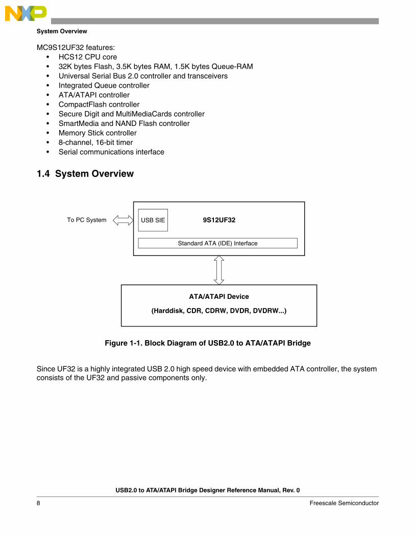
MC9S12UF32 features:• HCS12 CPU core• 32K bytes Flash, 3.5K bytes RAM, 1.5K bytes Queue-RAM• Universal Serial Bus 2.0 controller and transceivers• Integrated Queue controller• ATA/ATAPI controller• CompactFlash controller• Secure Digit and MultiMediaCards controller• SmartMedia and NAND Flash controller• Memory Stick controller• 8-channel, 16-bit timer • Serial communications interface
1.4 System Overview
Figure 1-1. Block Diagram of USB2.0 to ATA/ATAPI Bridge
Since UF32 is a highly integrated USB 2.0 high speed device with embedded ATA controller, the system consists of the UF32 and passive components only.
Standard ATA (IDE) Interface
USB SIE 9S12UF32
ATA/ATAPI Device
(Harddisk, CDR, CDRW, DVDR, DVDRW...)
To PC System

USB2.0 to ATA/ATAPI Bridge Designer Reference Manual, Rev. 0
Freescale Semiconductor 9
Chapter 2 Hardware Overview
2.1 Introduction
The system consists of the 64 pin package UF32 and passive components only. The major external component is an MOSFET used for 5V to 3.3V voltage regulation. There are two reference demo boards available: one is USB bus powered for 2.5" hard disk use, another is self-powered for 3.5" hard disk and ATAPI devices use.
Figure 2-1. USB Bus Powered Demo Board
Figure 2-2. Self-Powered Demo Board

Hardware Overview
USB2.0 to ATA/ATAPI Bridge Designer Reference Manual, Rev. 0
10 Freescale Semiconductor
2.2 Hardware Functions
Figure 2-3. Hardware Functions
The hardware functions can be divided into the following parts:• Voltage regulation• Background debug interface• USB interface• ATA interface
2.3 Voltage Regulation
The UF32 is designed for a single 5V voltage input. There are three kinds of I/Os:• Port E of 5V I/Os• Port J, M, and Q of 5V or 3.3V I/O powered by VDD3X• Port A, B, S, T, and U of 5V or 3.3V I/O powered by VDDX
However, for UF32 to be used in ATA applications VDD3X and VDDX must be with 3.3V, hence, only the port E is with 5V I/Os while the others are with 3.3V I/Os.
The UF32 has four built-in voltage regulators:• 3.3V regulator for USB transceiver and PLL use• 3.3V regulator (with a required external MOSFET) for I/O use• 2.5V regulator for S12 CPU core use• 2.5V regulator for USB transceiver use
The UF32 needs 5V power supplied to VDDR. The external MOSFET is regulated by the UF32 to provide 3.3V supply to VDD3X and VDDX. The USB transceivers and PLL are powered by the internal 3.3V regulator and the S12 CPU core is powered by the internal 2.5V regulator.
PORTE
PORTM
PORTJ
PORTQ
PORTT
PORTU
PORTS
PORTB
PORTA
BDM
USB
ATACORE
USB
REG
5V 3V2.5V
3V
5V
5V / 3.3V
3V
VDDA
VDDR
REF3V
VDD3X
VDDX
VDD Core
BKGD
USB Power
CS0–1, IOWR
DA0–2, IORD, DMACK
RESET
IORDY
DMARQ, INTRQ
D0–D7
D8–D15
MC9S12UF32
3V
5V
2.5V

Background Debug Interface
USB2.0 to ATA/ATAPI Bridge Designer Reference Manual, Rev. 0
Freescale Semiconductor 11
2.4 Background Debug Interface
The single-wired background debug pin BKGD is used for software development and programming.
2.5 USB Interface
The UF32 features an integrated Universal Serial Bus (USB) 2.0 controller and physical layer transceivers. An external 1.5kΩ pullup resistor, 510Ω reference resistor, and four serial resistors are required for USB connection. The USB power detection is used for self-powered system only.
2.6 ATA Interface
A standard 40 pin ATA connector is used. Only pullup, pulldown and serial termination resistors are needed to connect the UF32 to the ATA device. The ATA CSEL pin is shorted to ground and the firmware has fixed the device to be master, therefore the ATA/ATAPI device must be set for the option of either master or cable select.

Hardware Overview
USB2.0 to ATA/ATAPI Bridge Designer Reference Manual, Rev. 0
12 Freescale Semiconductor
USB2.0 to ATA/ATAPI Bridge Designer Reference Manual, Rev. 0
Freescale Semiconductor 13
Chapter 3 Software Overview
3.1 System Software Architecture
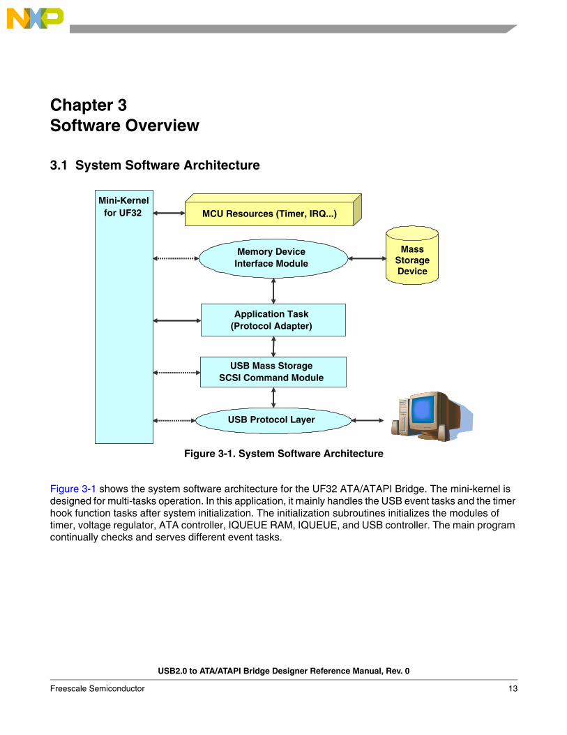
Figure 3-1. System Software Architecture
Figure 3-1 shows the system software architecture for the UF32 ATA/ATAPI Bridge. The mini-kernel is designed for multi-tasks operation. In this application, it mainly handles the USB event tasks and the timer hook function tasks after system initialization. The initialization subroutines initializes the modules of timer, voltage regulator, ATA controller, IQUEUE RAM, IQUEUE, and USB controller. The main program continually checks and serves different event tasks.
Mini-Kernelfor UF32 MCU Resources (Timer, IRQ...)
Interface ModuleMemory Device Mass
StorageDevice
(Protocol Adapter)Application Task
SCSI Command ModuleUSB Mass Storage
USB Protocol Layer
Software Overview
USB2.0 to ATA/ATAPI Bridge Designer Reference Manual, Rev. 0
14 Freescale Semiconductor
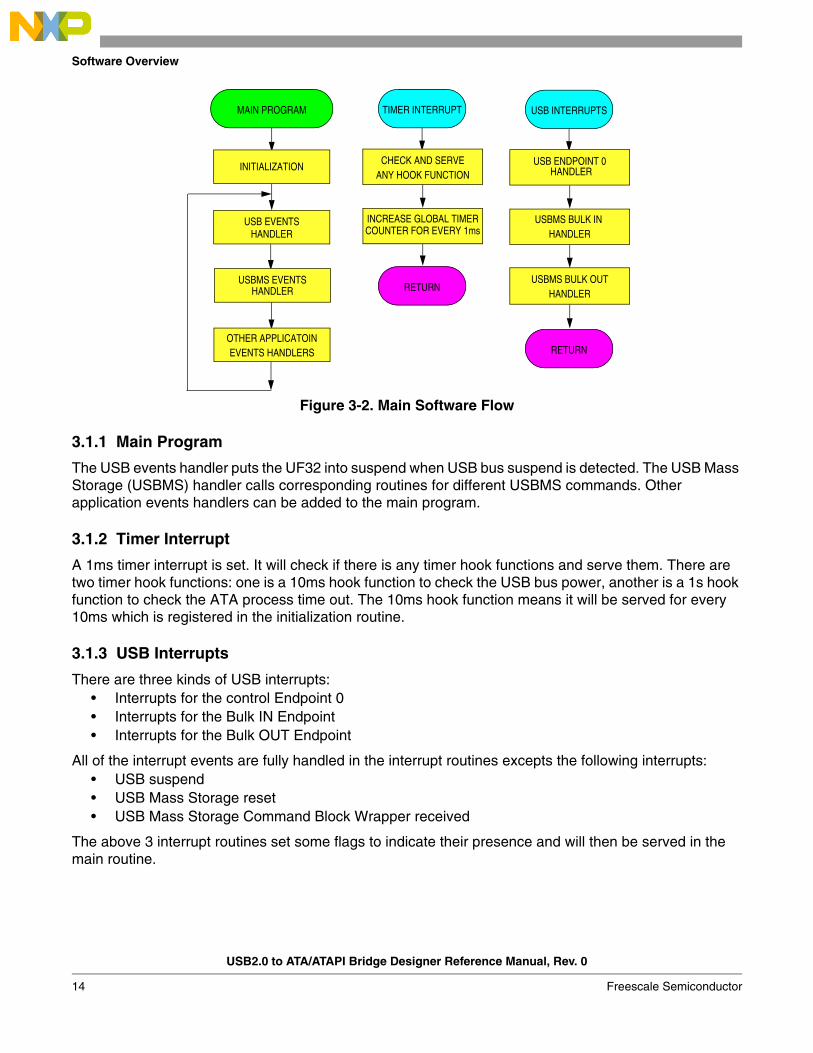
Figure 3-2. Main Software Flow
3.1.1 Main Program
The USB events handler puts the UF32 into suspend when USB bus suspend is detected. The USB Mass Storage (USBMS) handler calls corresponding routines for different USBMS commands. Other application events handlers can be added to the main program.
3.1.2 Timer Interrupt
A 1ms timer interrupt is set. It will check if there is any timer hook functions and serve them. There are two timer hook functions: one is a 10ms hook function to check the USB bus power, another is a 1s hook function to check the ATA process time out. The 10ms hook function means it will be served for every 10ms which is registered in the initialization routine.
3.1.3 USB Interrupts
There are three kinds of USB interrupts:• Interrupts for the control Endpoint 0• Interrupts for the Bulk IN Endpoint• Interrupts for the Bulk OUT Endpoint
All of the interrupt events are fully handled in the interrupt routines excepts the following interrupts:• USB suspend• USB Mass Storage reset• USB Mass Storage Command Block Wrapper received
The above 3 interrupt routines set some flags to indicate their presence and will then be served in the main routine.
MAIN PROGRAM
INITIALIZATION
USB EVENTS
TIMER INTERRUPT
CHECK AND SERVE
RETURN
INCREASE GLOBAL TIMERCOUNTER FOR EVERY 1ms
USBMS EVENTS
OTHER APPLICATOIN
HANDLER
USB INTERRUPTS
USB ENDPOINT 0HANDLER
USBMS BULK OUT
RETURN
USBMS BULK IN HANDLER
HANDLER
ANY HOOK FUNCTION
HANDLER
EVENTS HANDLERS

USB2.0 to ATA/ATAPI Bridge Designer Reference Manual, Rev. 0
Freescale Semiconductor 15
Chapter 4 USB Module
4.1 Introduction
The USB module consists of an integrated Universal Serial Bus (USB) 2.0 controller and physical layer transceivers to provide comprehensive USB specification implementation for both high-speed (480 Mbps) and full-speed (12 Mbps) operations.
4.2 Endpoints Configurations
Table 4-1 shows the endpoints configurations. The physical Endpoint 0 and Endpoint 1 are mapped to logical control Endpoint 0. The physical Endpoints 2 to 5 can be mapped to logical Endpoints 1 to 3. However, only one logical endpoint can be mapped to the logical endpoint 3. The USB host only sees the logical Endpoints.
The maximum buffer sizes of the Endpoints 4 and 5 are 64 bytes (full-speed) or 512 bytes (high-speed). IQUEUE RAM is used as the buffers for these two endpoints. The other endpoints are associated with dedicated 64 bytes of buffers.
In this application, only the control Endpoints and the physical Endpoints 4 and 5 are used.
Table 4-1. Endpoints Configurations
Physical Endpoint
LogicalEndpoint
TransferMode
TransferType
Maximum Buffer Size
0 0 SETUP CONTROL 64
10 IN CONTROL 64
0 OUT CONTROL 64
2 1 – 3 IN / OUT BULK / INT 64
3 1 – 3 IN / OUT BULK / INT 64
4 1 – 3 OUT ISO / BULK / INT 64 / 512
5 1 – 3 IN BULK / INT 64 / 512

USB Module
USB2.0 to ATA/ATAPI Bridge Designer Reference Manual, Rev. 0
16 Freescale Semiconductor

USB2.0 to ATA/ATAPI Bridge Designer Reference Manual, Rev. 0
Freescale Semiconductor 17
Chapter 5 IQUEUE Module
5.1 Introduction
The Intelligent Queue (IQUEUE) module allows automatic data transfer between the USB module and IQUEUE RAM, and between IQUEUE RAM and mass storage devices without CPU intervention. The IQUEUE RAM is configured to address $2000 to $25FF by writing 0x21 to the INITEE register.
Figure 5-1. IQUEUE Module
S12 CPU
USB
ATA/ATAPIDEVICE
IQUEUE RAMIQUEUEMODULE
USB IQRAM
IQRAM ATA

IQUEUE Module
USB2.0 to ATA/ATAPI Bridge Designer Reference Manual, Rev. 0
18 Freescale Semiconductor
5.2 IQUEUE Request Mapping
There are four IQUEUE channels of QC1 to QC4 which can be configured to transfer data to and from different peripherals. QC1 has the highest priority while QC4 has the lowest priority. QC1 and QC2, QC3 and QC4 can be configured as two double buffer channels. For the IQUEUE module to transfer data from one peripheral to another automatically, a single or double buffers channel with passing through mode must be used. For proper operation, the USB peripheral must use the channel with higher priority.
When writing data to an ATA/ATAPI device, QC1REQ is set to USB receive and QC2REQ is set to ATA transmit. When reading data from the device, QC3REQ is set to USB transmit and QC4REQ is set to ATA receive.
Table 5-1. IQUEUE Request Mapping
Data Flow QCnREQPeripheralFunctions
Direction
PC → USB → QRAM QC1REQ = 0 USB Rx
PC ← USB ← QRAM QC3REQ = 1 USB Tx
QRAM ← ATA QC4REQ = 2 ATA Rx
QRAM → ATA QC2REQ = 3 ATA Tx
4 CF Rx
5 CF Tx
6 MS Rx
7 MS Tx
8 SD Rx
9 SD Tx
10 SM Rx
11 SM Tx

USB2.0 to ATA/ATAPI Bridge Designer Reference Manual, Rev. 0
Freescale Semiconductor 19
Chapter 6 ATA Module
6.1 Introduction
The ATA host controller is designed according to the AT Attachment with Packet Interface–5 (ATA/ATAPI–5) specification. It can support PIO mode 0 to 4 and UDMA mode 0 to 4 with maximum burst transfer rate of 60M bytes per second.
The firmware is written according to the ATA/ATAPI–6 specification, therefore it can support higher than 137G byte capacity.
6.2 ATA Registers
Table 6-1 summarizes the ATA registers. There are two types of registers: (1) controls the ATA controller and (2) registers mapped to external ATA/ATAPI device. There are special procedures to read and write to the ATA device registers.
Table 6-1. ATA Registers
Registers Description
Host Configuration Register Configure ATA host controller
Host Status Register Host controller operating status
PIO Timing Registers 1–4 Timing registers for PIO, DMA and UDMA modes. One Timing unit is 1/60MHz.(i.e.: 1 in the register represents 16.67ns)
Multi-Word DMA Timing Registers 1–4
UDMA Timing Registers 1–9
ATA Drive Control Register (write)ATA Drive Alternate Status Register (read)
These registers are mapped to external ATA device registers with the same names based on the ATA5 specifications except the DMA Mode Register which is for the ATA host controller to operate in DMA mode or not.
ATA Drive Data Register
ATA Drive Feature Register
ATA Drive Error Register
ATA Drive Sector Count Register
ATA Drive Sector Number Register
ATA Drive Cylinder Low Register
ATA Drive Cylinder High Register
ATA Drive Device/Head Register
ATA Drive Cylinder High Register
ATA Drive Command and DMA Mode Register (write)ATA Drive Status Register (read)

ATA Module
USB2.0 to ATA/ATAPI Bridge Designer Reference Manual, Rev. 0
20 Freescale Semiconductor
6.2.1 Write to ATA Device Registers1. Wait if TIP of the Host Status Register = 12. ATA device register = data3. Wait if DRAB = 1
6.2.2 Read from ATA Device Registers1. Wait if TIP of the Host Status Register = 12. Data = ATA device register (dummy read)3. Wait if DRAB = 14. Data = ATA device register

USB2.0 to ATA/ATAPI Bridge Designer Reference Manual, Rev. 0
Freescale Semiconductor 21
Chapter 7 USB Mass Storage Interface Driver
7.1 Introduction
The driver is implemented according to the specification of the USB Mass Storage Class Bulk-Only Transport and the specification of the Small Computer Computer Interface 2.
We have chosen the Bulk-Only Transport rather than the Command Bulk Interrupt because the drivers for the Bulk-Only Transport are embedded in the Windows 2000 and the Windows XP operating systems. Regarding the endpoints usage, one bulk IN and one bulk OUT endpoints together with the control endpoints are needed. The subclass of the SCSI Transparent command 0x06 is used since the SCSI command can support most storage and multimedia devices.
7.2 USB Mass Storage Class Bulk-Only Transport
In Bulk-Only Transport, transport of command, data, and status occurs solely via Bulk endpoints. There are two class specific requests through the SETUP command:
• Bulk-Only Mass Storage Reset• Get Max LUN
The Bulk-Only Mass Storage Reset is to reset the mass storage device and its associated interface. The Get Max LUN is used to get the number of logical units the device supports.
The host shall send out a Command Block Wrapper through an OUT endpoint before sending out data or requesting the device to return data. The device then responds with the Command Status Wrapper. Figure 7-1 shows the command data status flow.

USB Mass Storage Interface Driver
USB2.0 to ATA/ATAPI Bridge Designer Reference Manual, Rev. 0
22 Freescale Semiconductor
Figure 7-1. Command Data Status Flow
7.2.1 USB Command Block Wrapper
The host sends each Command Block Wrapper containing a command block to the device via the Bulk-OUT endpoint. The Command Block is represented by the bits 15 to 30 of the CBW. Our device supports the sub-class code of 0x06 of the SCSI Transparent Command Set.
Table 7-1. Command Block Wrapper
bitbyte
7 6 5 4 3 2 1 0
0–3LSB (Byte 0)MSB (Byte 3)
dCBWSignature(0x55 0x53 0x42 0x43)
4–7 dCBWTag
8–11 dCBWDataTransferLength (number of bytes of data transfer expected)
12 bmCBWFlags13 Reserved (0) bCBWLUN (logical device number)
14 Reserved (0) bCBWCBLength (Command Block length)
15–30 bCBWCB (Command Block)
READY
HOST SENDS OUT CBW
OUT
DATAx 31 BYTE CBW
HOST SENDS OUT DATA
OUT
DATAx DATA
IN
DATAx DATA
DEVICE RETURNS DATA
MORE DATATO SEND?
MORE DATATO RECEIVE?
IN
DATAx 13 BYTE CSW
DEVICE RETURNS CSW
YES
NO
YES
NO

USB Mass Storage Class Bulk-Only Transport
USB2.0 to ATA/ATAPI Bridge Designer Reference Manual, Rev. 0
Freescale Semiconductor 23
7.2.2 USB Command Status Wrapper
The USB Command Status Wrapper (CSW) starts on a packet boundary and ends as a short packet with exactly 13 bytes transferred. The bCSWStatus indicates the success or failure of the command. The device shall set this byte to zero if the command is completed successfully, to 1 if failed, and to 2 for phase error. The host shall perform a Reset Recovery when phase error status is returned in the CSW.
7.2.3 SCSI Command Descriptor Block
The SCSI Command Descriptor Block (CDB) always has an operation code as the first byte and the control byte as its last byte. For any command, if there is an invalid parameter in the CDB, the target should terminate the command without altering the medium.
Table 7-2. Command Status Wrapper
7 6 5 4 3 2 1 0
0–3 dCSWSignature (0x55 0x53 0x42 0x53)4–7 dCSWTag (get from the CBW)
8–11dCSWDataResidule
(number of bytes different between expected transfer length and actual handled)
12 bmCSWStatus
Table 7-3. CDB of 6-Byte Command
7 6 5 4 3 2 1 0
0 Operation Code
1–3dCBWTag (MSB)
Logical Block Address (if required)(LSB)
4Transfer Length (if required)
Parameter List Length (if required)Allocation Length
5 Control
Table 7-4. CDB of 10-Byte Command
7 6 5 4 3 2 21 0
0 Operation Code
1 Reserved (0) Service Action (if required)2–5 (MSB byte 2) Logical Block Address (if required) (LSB byte 5)
6 Reserved (0)
7–8(MSB byte 7) Transfer Length (if required)
Parameter List Length (if required)Allocation length (if required) (LSB byte 8)
9 Control

USB Mass Storage Interface Driver
USB2.0 to ATA/ATAPI Bridge Designer Reference Manual, Rev. 0
24 Freescale Semiconductor
Table 7-5. CDB of 12-Byte Command
7 6 5 4 3 2 21 00 Operation Code
1 Reserved (0) Service Action (if required)
2–5 (MSB byte 2) Logical Block Address (if required) (LSB byte 5)
6–9(MSB byte 6) Transfer Length (if required)
Parameter List Length (if required)Allocation length (if required) (LSB byte 9)
10 Reserved
11 Control
Table 7-6. CDB of 16-Byte Command
7 6 5 4 3 2 21 00 Operation Code1 Reserved (0) Service Action (if required)
2–5 (MSB byte 2) Logical Block Address (if required) (LSB byte 5)
6–9 (MSB byte 6) Additional CDB Data (if required) (LSB byte 9)
10–13(MSB byte 10) Transfer Length (if required)
Parameter List Length (if required)Allocation length (if required) (LSB byte 13)
14 Reserved15 Control
Table 7-7. CDB of Long LBA 16-Byte Command
7 6 5 4 3 2 21 0
0 Operation Code1 Reserved (0) Service Action (if required)
2–9 (MSB byte 2) Logical Block Address (if required) (LSB byte 9)
10–13(MSB byte 10) Transfer Length (if required)
Parameter List Length (if required)Allocation length (if required) (LSB byte 13)
14 Reserved
15 Control

Driver Structure
USB2.0 to ATA/ATAPI Bridge Designer Reference Manual, Rev. 0
Freescale Semiconductor 25
7.2.4 Example of Command Block Wrapper
Table 7-8 shows a USB CBW issued to the device number 0 (byte 12 of the CBW) with effective SCSI command length of 10 (byte 14). The expected transfer length is 0x1000, i.e. Byte 11 (MSB) to Byte 8 (LSB).
The “2A” in byte 15 of the CBW means it is a SCSI Write_10 command. The command requests the device to write 8 blocks of data to the LBA 0x9C4637. In this example one block of data equals 512 bytes. Therefore, 8 blocks of data equal 4K bytes which matches the expected transfer length of 0x1000 bytes of data length requested in the CBW.
7.3 Driver Structure
The driver handles and responds to the commands included in the USB Command Block Wrapper and the Class Specific Requests.
7.3.1 Handling of USB Command Block Wrapper
Figure 7-2 shows the handling of the USB Command Block Wrapper, which is a detail implementation including errors handling. There are only three kinds of commands to handles:
• Commands without data transfer• Host sends out data to storage device• Host receives data from storage device
After decoding the SCSI command from the CBW, the driver will either:• handle the command without interfering with the individual storage device driver, or• translate the command and call individual routines of the storage device driver.
After receiving a 31 byte CBW and all data has been transferred, the UF32 will return a 13 byte CSW to the host with either a result of pass or fail which depends on the global variable gUSBMSResult. Pass result only happens if the command is supported and the storage device has successfully executed the command.
Table 7-8. Example of a CBW containing SCSI Write_10 Command
USB CBW SCSI Command
Bytes Data (HEX) Bytes Data (HEX) Meaning
0–3 55 53 42 43 (Signature) 0 2A Write_10
4–7 A8 1A A4 FF (Tag) 1 00 Not used
8–11 00 10 00 00 (Length)2–5 00 9C 46 37
Logical Block Address12 00 (Device Number)
13 00 (Reserved)6–9 00 00 00 08
Number of blocks to transfer14 0A (Command Length)
15–302A 00 00 9C 46 37 00 0000 08 00 00 00 00 00 00
10–1500 00 00 00 00 00
Not used

USB Mass Storage Interface Driver
USB2.0 to ATA/ATAPI Bridge Designer Reference Manual, Rev. 0
26 Freescale Semiconductor
Figure 7-2. CSW Command Handling
COMMAND
SUCCESS?
HOST SENDS OUT CBW
OUT
DATAx 31 BYTE CBW
HOST SENDS OUT DATA
DATAx DATA
IN
DATAx DATA
DEVICE RETURNS DATAERRORFOUND?
HOST RECEIVES
ALL DATA?
IN
DATAx 13 BYTE CSW
DEVICE RETURNS CSW
YES
SCSI COMMAND
HANDLING
NO DATA TRANSFER
IS EXPECTED
HOST TO RECEIVE
DATA FROM DEVICEHOST TO SEND DATA
TO DEVICE
COMMAND
SUPPORTED?
COMMANDCOMMAND
SUPPORTED?
STALLIN
STALLOUT
ENDPOINT
gUSBCSWResult
= Failed
gUSBCSWResult
= Failed
IN
DATAx DATA
RETURNS ZEROLENGTH DATA
COMMAND
SUCCESS?
gUSBCSWResult
= Failed
COMMAND
SUCCESS?
gUSBCSWResult
= Failed
YES YES
NONO NO
YES
YES
NO
YES
NO
YES
NONO
NO
DEVICE RECEIVESALL DATA?
DEVICE RECEIVESALL DATA?
HOST RECEIVES
ALL DATA?
NO
YESYES
YES
NO
NO
NOOUT
YESIN
SUPPORTED?
ERROR FOUND?
YES

Driver Structure
USB2.0 to ATA/ATAPI Bridge Designer Reference Manual, Rev. 0
Freescale Semiconductor 27
7.3.1.1 Commands Without Data Transfer
Since no data transfer is required. After processing the CBW, the UF32 will return the 13 bytes of CBW.
7.3.1.2 Host Sends out Data to Storage Device
After sending out a 31 byte CBW, the host continues to send data to the UF32. If error happens and the UF32 has not acknowledge (ACK) all the data from the host, the OUT endpoint is STALLED to inform the host that the UF32 is not able to accept further data. After the UF32 receives all the data from host and sends all the data to the storage, it will check whether the device has successfully received the data without any error.
7.3.1.3 Host Receives Data from Storage Device
After sending out a 31 byte CBW, the host expects the storage device to send out data. If error happens and the host has not acknowledge (ACK) all the data from the device, a zero length data will be sent out for next IN token to inform the host that there is no more data to transfer.
7.3.2 Class Specific Request
There are two class specific requests through the SETUP command, the Bulk-Only Mass Storage Reset and the Get Max LUN.
The driver responds to the Get Max LUN command by returning one byte of maximum LUN with value from 0 to 15 representing logical unit number 1 to 16.
After receiving the Bulk-Only Mass Storage Reset, the driver calls the reset routines of the registered storage devices one by one.
The driver returns STALL to other reserved class specific requests.
Figure 7-3. Software Flow of Class Specific Request
SETUP
DATA0 8 BYTE CBW
GET MAX LUN
IN
DATAx 1 BYTE LUN
DEVICE RETURNS LUN
HOST SENDS OUT
(bRequest = 0xFE)
BULK-ONLY MASSSTORAGE RESET
OTHERS(bRequest = 0x00 to 0xFD)
(bRequest = 0xFF)
RESET DEVICES STALL
CLASS SPECIFIC REQUESTS
IN
STALL
RETURN

USB Mass Storage Interface Driver
USB2.0 to ATA/ATAPI Bridge Designer Reference Manual, Rev. 0
28 Freescale Semiconductor
USB2.0 to ATA/ATAPI Bridge Designer Reference Manual, Rev. 0
Freescale Semiconductor 29
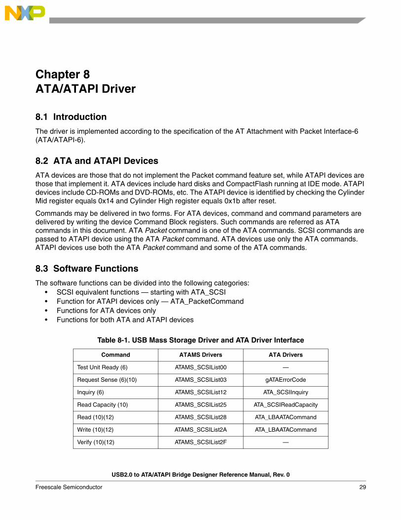
Chapter 8 ATA/ATAPI Driver
8.1 Introduction
The driver is implemented according to the specification of the AT Attachment with Packet Interface-6 (ATA/ATAPI-6).
8.2 ATA and ATAPI Devices
ATA devices are those that do not implement the Packet command feature set, while ATAPI devices are those that implement it. ATA devices include hard disks and CompactFlash running at IDE mode. ATAPI devices include CD-ROMs and DVD-ROMs, etc. The ATAPI device is identified by checking the Cylinder Mid register equals 0x14 and Cylinder High register equals 0x1b after reset.
Commands may be delivered in two forms. For ATA devices, command and command parameters are delivered by writing the device Command Block registers. Such commands are referred as ATA commands in this document. ATA Packet command is one of the ATA commands. SCSI commands are passed to ATAPI device using the ATA Packet command. ATA devices use only the ATA commands. ATAPI devices use both the ATA Packet command and some of the ATA commands.
8.3 Software Functions
The software functions can be divided into the following categories:• SCSI equivalent functions — starting with ATA_SCSI• Function for ATAPI devices only — ATA_PacketCommand• Functions for ATA devices only• Functions for both ATA and ATAPI devices
Table 8-1. USB Mass Storage Driver and ATA Driver Interface
Command ATAMS Drivers ATA Drivers
Test Unit Ready (6) ATAMS_SCSIList00 —
Request Sense (6)(10) ATAMS_SCSIList03 gATAErrorCode
Inquiry (6) ATAMS_SCSIList12 ATA_SCSIInquiry
Read Capacity (10) ATAMS_SCSIList25 ATA_SCSIReadCapacity
Read (10)(12) ATAMS_SCSIList28 ATA_LBAATACommand
Write (10)(12) ATAMS_SCSIList2A ATA_LBAATACommand
Verify (10)(12) ATAMS_SCSIList2F —

ATA/ATAPI Driver
USB2.0 to ATA/ATAPI Bridge Designer Reference Manual, Rev. 0
30 Freescale Semiconductor
SCSI commands are passed to ATAPI devices by calling the ATA Packet command. Therefore, for ATAPI devices, the USBMS driver will directly call the ATA_PacketCommad() and passes the SCSI CDB parameters to the devices.
For ATA devices, the USBMS driver will either:• handle the command without calling the ATA Driver, or• call the ATA_SCSI commands, or• call the ATA_LBAATACommand for read and write commands.
Recall from the last section that there are only three kinds of USB CBW commands.
8.3.1 Commands Without Data Transfer
For ATAPI device, the USBMS Driver will call the ATAMS_ATAPI routine.
For ATA device, there are two commands supported:• Test Unit Ready• Verify
For Test Unit Ready Command, the USBMS Driver always returns pass that means the device is always ready.
The Verify Command is used in Full-Format, the USBMS Driver always returns pass.
8.3.2 Host Sends out Data to ATA/ATAPI Device
For ATAPI device, the USBMS Driver calls the ATAMS_ATAPIWrite routine.
For ATA device, only write command is supported in which host writes data into device. The command is handled by the ATAMS_SCSIList2A routine setting up the IQUEUE channels and calling the ATA_LBAATACommand routine.
8.3.3 Host Receives Data from ATA/ATAPI Device
For ATAPI device, the USBMS Driver calls the ATAMS_ATAPIRead routine.
For ATA device, the commands supported are:• Request Sense (device returns error code of the global variable gATAErrorCode to host)• Inquiry (device returns ATA information to host by the ATA_SCSIInquiry routine)• Read Capacity (device returns total capacity to host by the ATA_SCSIReadCapacity routine)• Read (device returns data to host by the ATA_SCSIList28 routine setting up the IQUEUE channels
and calling the ATA_LBAATACommand routines
8.3.4 Individual Software Function
All functions can be used by both ATA and ATAPI devices except those specified. All functions return the ATA error code which is defined according to Table 8-2.

Software Functions
USB2.0 to ATA/ATAPI Bridge Designer Reference Manual, Rev. 0
Freescale Semiconductor 31
The following tables show the summary of all the ATA/ATAPI drivers.
Table 8-2. ATA Error Code Definitions
Error Code Description0x00 Command Passed0x01 Command Failed
0x02 Unrecoverable Error (e.g. timeout)
ATA_PacketCommandDescription ATA Packet Command for ATAPI devices only
Inputmuint16 *pCommand6 or 8 words of ATAPI command
Output nil
Return ATAErrorCode
ATA_SoftwareResetDescription Software reset to ATA/ATAPI devices
Input nil
Output nil
Return ATAErrorCode
ATA_PIOReadCommandDescription Read ATA or ATAPI device using PIO mode
Input
muint16 *pBufferbuffer pointer for data to put intomuint16 XferLennumber of words to be read from the device
Output data put into buffer
Return ATAErrorCode
ATA_PIOWriteCommandDescription Write to ATA or ATAPI device using PIO mode
Input
muint16 *pBufferbuffer pointer for data to put intomuint16 XferLennumber of words to be written to the device
Output data put into device
Return ATAErrorCode

ATA/ATAPI Driver
USB2.0 to ATA/ATAPI Bridge Designer Reference Manual, Rev. 0
32 Freescale Semiconductor
ATA_SCSIInquiry
DescriptionHandle SCSI Inquiry Command by getting the ATA/ATAPI devices information and put corresponding data into buffer
Input
muint16 *pBufferbuffer pointer of 24 words for storing temporary data and resultmuint16 XferLentransfer length in byte specified in the SCSI command
Output 32 bytes of SCSI Inquiry result into the buffer
Return ATAErrorCode
ATA_SCSIReadCapacityDescription Handle SCSI Read Capacity Command by returning data into buffer
Inputmuint16 *pBufferbuffer pointer of 4 byte length for data to put into
Output data put into buffer
Return ATAErrorCode
ATA_WaitRegBusyDescription Wait until ATA hardware module is ready
Input nilOutput nil
Return ATAErrorCode
ATA_WaitATABusyDescription Wait until ATA/ATAPI device is ready
Input nilOutput nil
Return ATAErrorCode
ATA_SetPIOTimingDescription Set ATA hardware module timing in PIO mode
Inputmuint8 PIOModePIO mode 0–4
Output nilReturn ATAErrorCode
Software Functions
USB2.0 to ATA/ATAPI Bridge Designer Reference Manual, Rev. 0
Freescale Semiconductor 33
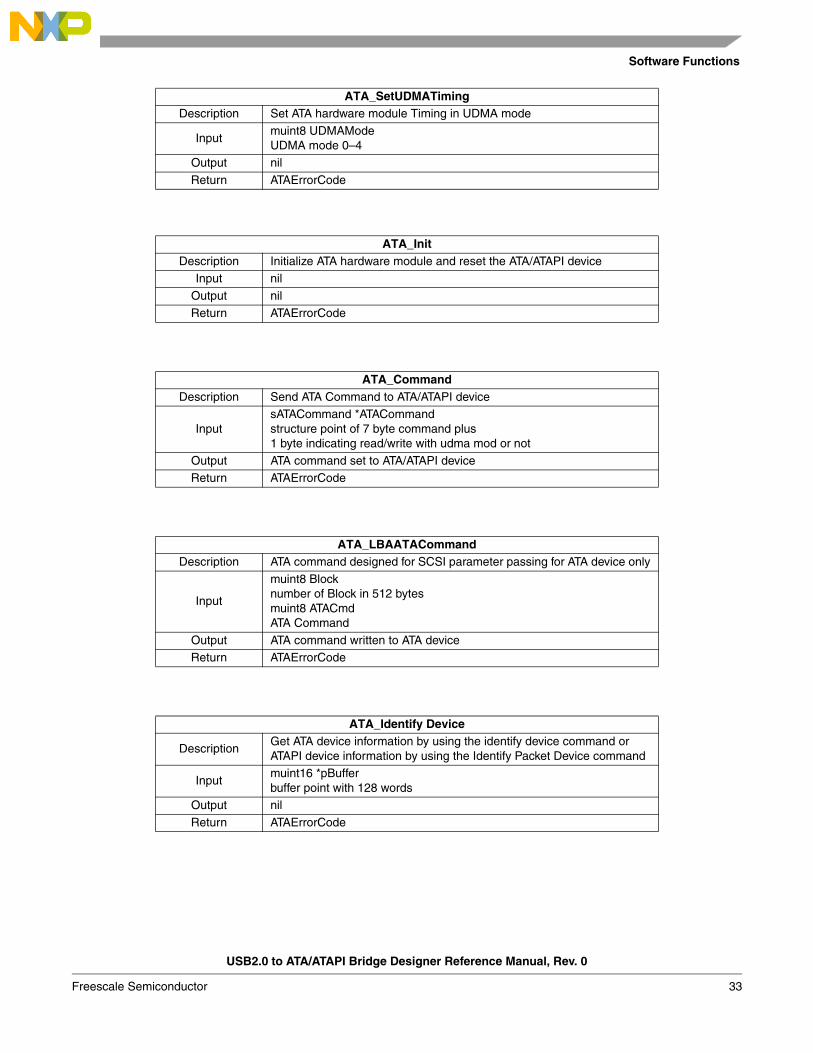
ATA_SetUDMATimingDescription Set ATA hardware module Timing in UDMA mode
Inputmuint8 UDMAModeUDMA mode 0–4
Output nil
Return ATAErrorCode
ATA_InitDescription Initialize ATA hardware module and reset the ATA/ATAPI device
Input nil
Output nil
Return ATAErrorCode
ATA_CommandDescription Send ATA Command to ATA/ATAPI device
InputsATACommand *ATACommandstructure point of 7 byte command plus1 byte indicating read/write with udma mod or not
Output ATA command set to ATA/ATAPI deviceReturn ATAErrorCode
ATA_LBAATACommandDescription ATA command designed for SCSI parameter passing for ATA device only
Input
muint8 Blocknumber of Block in 512 bytesmuint8 ATACmdATA Command
Output ATA command written to ATA deviceReturn ATAErrorCode
ATA_Identify Device
DescriptionGet ATA device information by using the identify device command or ATAPI device information by using the Identify Packet Device command
Inputmuint16 *pBufferbuffer point with 128 words
Output nil
Return ATAErrorCode
ATA/ATAPI Driver
USB2.0 to ATA/ATAPI Bridge Designer Reference Manual, Rev. 0
34 Freescale Semiconductor
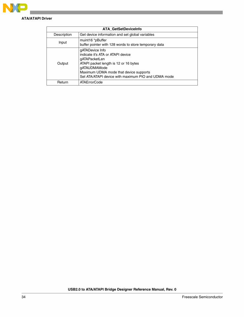
ATA_GetSetDeviceInfo
Description Get device information and set global variables
Inputmuint16 *pBufferbuffer pointer with 128 words to store temporary data
Output
gATADevice Infoindicate it’s ATA or ATAPI devicegATAPacketLenATAPI packet length is 12 or 16 bytesgATAUDMAModeMaximum UDMA mode that device supportsSet ATA/ATAPI device with maximum PIO and UDMA mode
Return ATAErrorCode

USB2.0 to ATA/ATAPI Bridge Designer Reference Manual, Rev. 0
Freescale Semiconductor 35
Chapter 9 Test and Customization
9.1 Testing
This reference design was tested with different ATA/ATAPI devices and under different Windows Operating Systems on several different PCs.
• USB compliance test using Command Verifier version 1.21• Compatibility tests under Windows 98 SE, 2000 and XP• Compatibility tests under AMD 750, Intel 810 and 865 chip set Desktops, and IBM Thinkpad T23.
9.2 Customization
9.2.1 Hardware
There are some circuits present in the schematic but absent in the printed circuit board. You have to modify the PCB according to your applications. There are three kinds of supported applications:
• Self-powered• Bus-powered• Amadeus
9.2.1.1 Self-powered
Add the USB bus power detection circuitry as shown in the schematic.
9.2.1.2 Bus-powered
Please note that for ATA USB bus-powered application a special USB cable is needed to draw current from another USB port or from a PS2 port. Since this kind of application violates the USB specification, operation stability depends on the PC systems and the ATA devices.
9.2.1.3 Amadeus
Add the PE7 pin circuitry as shown in the schematic. Amadeus is a 32-bit Coldfire chip designed for multimedia applications. The UF32, together with the Amadeus form a USB2.0 multimedia platform. For a multimedia platform using harddisk, the UF32 operation is controlled by the PE7 pin. A logic high on the pin puts the UF32 into normal ATA/ATAPI bridge application. A logic low on the pin puts the UF32 into STOP and the UF32 then releases the ATA bus for Amadeus to access the ATA device. A logic high on PE7, followed by an external reset or interrupt (negative pulse) is required to wake up the UF32 to enable it to work again as a normal ATA/ATAPI bridge.

Test and Customization
USB2.0 to ATA/ATAPI Bridge Designer Reference Manual, Rev. 0
36 Freescale Semiconductor
9.2.2 Firmware
There are six targets created in the Codewarrior version 3.1 project:• Development (100-pin)• Development (64-pin)• Self-powered (64-pin)• Bus-powered (64-pin)• Amadeus (64-pin)• Amadeus (100-pin)
The project file is under the “Application” directory. The project supports the self-powered demo board (64-pin), the USB bus-powered demo board (64-pin), and the M68KIT912UF32 board (100-pin).
A proper project must be chosen according to the application. When using the development project, if you unplug and replug the USB connector, the system may not work.
You must choose the self-powered, bus-powered or Amadeus target as a reference for your end product. It works normally when you unplug and re-plug the USB connector.


How to Reach Us:
Home Page:www.freescale.com
E-mail:[email protected]
USA/Europe or Locations Not Listed:Freescale SemiconductorTechnical Information Center, CH3701300 N. Alma School RoadChandler, Arizona 85224+1-800-521-6274 or [email protected]
Europe, Middle East, and Africa:Freescale Halbleiter Deutschland GmbHTechnical Information CenterSchatzbogen 781829 Muenchen, Germany+44 1296 380 456 (English)+46 8 52200080 (English)+49 89 92103 559 (German)+33 1 69 35 48 48 (French)[email protected]
Japan:Freescale Semiconductor Japan Ltd.HeadquartersARCO Tower 15F1-8-1, Shimo-Meguro, Meguro-ku,Tokyo 153-0064Japan0120 191014 or +81 3 5437 [email protected]
Asia/Pacific:Freescale Semiconductor Hong Kong Ltd.Technical Information Center2 Dai King StreetTai Po Industrial EstateTai Po, N.T., Hong Kong+800 2666 [email protected]
For Literature Requests Only:Freescale Semiconductor Literature Distribution CenterP.O. Box 5405Denver, Colorado 802171-800-441-2447 or 303-675-2140Fax: [email protected]
Information in this document is provided solely to enable system and software implementers to use Freescale Semiconductor products. There are no express or implied copyright licenses granted hereunder to design or fabricate any integrated circuits or integrated circuits based on the information in this document.
Freescale Semiconductor reserves the right to make changes without further notice to any products herein. Freescale Semiconductor makes no warranty, representation or guarantee regarding the suitability of its products for any particular purpose, nor does Freescale Semiconductor assume any liability arising out of the application or use of any product or circuit, and specifically disclaims any and all liability, including without limitation consequential or incidental damages. “Typical” parameters that may be provided in Freescale Semiconductor data sheets and/or specifications can and do vary in different applications and actual performance may vary over time. All operating parameters, including “Typicals”, must be validated for each customer application by customer’s technical experts. Freescale Semiconductor does not convey any license under its patent rights nor the rights of others. Freescale Semiconductor products are not designed, intended, or authorized for use as components in systems intended for surgical implant into the body, or other applications intended to support or sustain life, or for any other application in which the failure of the Freescale Semiconductor product could create a situation where personal injury or death may occur. Should Buyer purchase or use Freescale Semiconductor products for any such unintended or unauthorized application, Buyer shall indemnify and hold Freescale Semiconductor and its officers, employees, subsidiaries, affiliates, and distributors harmless against all claims, costs, damages, and expenses, and reasonable attorney fees arising out of, directly or indirectly, any claim of personal injury or death associated with such unintended or unauthorized use, even if such claim alleges that Freescale Semiconductor was negligent regarding the design or manufacture of the part.
Freescale™ and the Freescale logo are trademarks of Freescale Semiconductor, Inc.All other product or service names are the property of their respective owners.
© Freescale Semiconductor, Inc. 2005. All rights reserved.
DRM062Rev. 0, 1/2005


