IEEE1394 to ATA/ATAPI Native Bridge Data Sheet …. The 1394 transaction layer and SBP-2 protocol is...
32
Oxford Semiconductor Ltd. 25 Milton Park, Abingdon, Oxon, OX14 4SH, UK Tel: +44 (0)1235 824900 Fax: +44(0)1235 821141 Oxford Semiconductor 2001 OXFW911 Data Sheet Revision 1.1 – Mar 2001 Part No. OXFW911-TQ- A FEATURES • S400 (50 Mbytes/s) compliant 1394-1995 Link and Transaction layers • Compatible with 1394-1995 and 1394A Phys. • Microsoft Win98-Second Edition, Win2000 and Apple MacOS generic driver support • SBP-2 Target Revision 4 compliant interface • Fully ATA-5 compliant (see T13-1321D) • Support for UDMA5 (ATA100) • Sustained data transfer of 35 MB/s • Supports PIO modes 0 to 4, DMA modes 0 to 2 and Ultra DMA modes 0 to 5 • ORB co-processor to accelerate translation of ORBs to ATAPI commands • Supports ORB chaining for increased performance • High performance ATA command translation in firmware using Reduced Block Command (RBC) set • Integrated 32-bit RISC processor (ARM7TDMI) with on-chip scratch RAM • Optional External Serial ROM interface for configuration data, user serial number, etc. • Integrated 512kb Flash memory • Blank Flash memory programming feature via 1394 bus • Firmware and Flash Programming Utilities supplied by Oxford Semiconductor • 3.3 Volts operation • Low Power CMOS • Ultra-thin 128-TQFP package (14 x 14 x 1 mm) DESCRIPTION The OXFW911 is a high-performance 1394 to ATA/ATAPI (IDE) native bridge with an integrated target Serial Bus Protocol (SBP-2 ) controller. By supporting the SBP-2 protocol, the device can use generic SBP-2 drivers available in the Microsoft Windows 98SE, Microsoft Windows 2000, Microsoft Millennium and Apple MacOS (8.4 to 9.04) operating systems. MacOS support also includes booting from Firewire disk. The device is ideally suited for smart-cable or tailgate interface applications for removable-media drives, compact flash card readers, CD-ROM, CD-R, CD-RW, DVD-ROM, DVD-RAM and hard disk drives, allowing IDE drives to be connected to a 1394 serial bus in a plug-and-play fashion. Both ATA and ATAPI devices are supported using the same firmware. This highly integrated device offers a two-chip solution to native bridge applications using an external 1394 PHY. The device is compatible with both 1394-1995 and 1394A PHYs. The LINK controller complies with 1394-1995 and 1394A specifications. The 1394 transaction layer and SBP-2 protocol is implemented using a combination of the ARM7TDMI (low-power 32-bit RISC processor), an ORB (Operational Request Block) hardware co-processor and a high performance buffer manager. The buffer manager has a RAM bandwidth of 800Mbps. It provides storage for 1394 and ATA/ATAPI packets, automatically storing them and passing them to the appropriate destinations, without any intervention from the processor. It also provides storage and manages the sequencing of ORB fetching to reduce latency and improve data throughput. The configuration data including the IEEE OUI (Organisational Unique Identifier) and device serial number is stored in the Flash ROM which may be uploaded from the 1394 bus, even when blank. The device also facilitates firmware uploads from the 1394 bus. The ORB co-processor translates ORBs as defined in the SBP-2 protocol into ATA/ATAPI commands, and automatically stores error/status messages at an address specified by the host. Concurrent operation of the ATA/ATAPI and 1394 interfaces are facilitated using the high throughput buffer manager where LINK, ATAPI manager and ARM7TDMI can perform interleaved accesses to the on-chip RAM buffer. The high performance processor ensures that no significant latency is incurred. The ATA command translation is performed in firmware to meet RBC (Reduced Block Commands) standard, T10-1228D. The ATA/ATAPI Manager supports PIO modes 0 to 4, DMA modes 0 to 2 and Ultra DMA mode 0 to 5 and provides the interface to the IDE bus. It is compliant with T13-1321D, ATA-5 specification, as well as support for ATA100. OXFW911 IEEE1394 to ATA/ATAPI Native Bridge Data Sheet
Transcript of IEEE1394 to ATA/ATAPI Native Bridge Data Sheet …. The 1394 transaction layer and SBP-2 protocol is...

Oxford Semiconductor Ltd. 25 Milton Park, Abingdon, Oxon, OX14 4SH, UK Tel: +44 (0)1235 824900 Fax: +44(0)1235 821141
Oxford Semiconductor 2001OXFW911 Data Sheet Revision 1.1 – Mar 2001
Part No. OXFW911-TQ-A
FEATURES
• S400 (50 Mbytes/s) compliant 1394-1995 Link and Transaction layers
• Compatible with 1394-1995 and 1394A Phys. • Microsoft Win98-Second Edition, Win2000 and Apple
MacOS generic driver support • SBP-2 Target Revision 4 compliant interface • Fully ATA-5 compliant (see T13-1321D) • Support for UDMA5 (ATA100) • Sustained data transfer of 35 MB/s • Supports PIO modes 0 to 4, DMA modes 0 to 2 and
Ultra DMA modes 0 to 5 • ORB co-processor to accelerate translation of ORBs
to ATAPI commands • Supports ORB chaining for increased performance
• High performance ATA command translation in firmware using Reduced Block Command (RBC) set
• Integrated 32-bit RISC processor (ARM7TDMI) with on-chip scratch RAM
• Optional External Serial ROM interface for configuration data, user serial number, etc.
• Integrated 512kb Flash memory • Blank Flash memory programming feature via 1394
bus • Firmware and Flash Programming Utilities supplied by
Oxford Semiconductor • 3.3 Volts operation • Low Power CMOS • Ultra-thin 128-TQFP package (14 x 14 x 1 mm)
DESCRIPTION
The OXFW911 is a high-performance 1394 to ATA/ATAPI (IDE) native bridge with an integrated target Serial Bus Protocol (SBP-2 ) controller. By supporting the SBP-2 protocol, the device can use generic SBP-2 drivers available in the Microsoft Windows 98SE, Microsoft Windows 2000, Microsoft Millennium and Apple MacOS (8.4 to 9.04) operating systems. MacOS support also includes booting from Firewire disk. The device is ideally suited for smart-cable or tailgate interface applications for removable-media drives, compact flash card readers, CD-ROM, CD-R, CD-RW, DVD-ROM, DVD-RAM and hard disk drives, allowing IDE drives to be connected to a 1394 serial bus in a plug-and-play fashion. Both ATA and ATAPI devices are supported using the same firmware. This highly integrated device offers a two-chip solution to native bridge applications using an external 1394 PHY. The device is compatible with both 1394-1995 and 1394A PHYs. The LINK controller complies with 1394-1995 and 1394A specifications. The 1394 transaction layer and SBP-2 protocol is implemented using a combination of the ARM7TDMI (low-power 32-bit RISC processor), an ORB (Operational Request Block) hardware co-processor and a high performance buffer manager. The buffer manager has a RAM bandwidth of 800Mbps. It provides storage for 1394 and ATA/ATAPI packets,
automatically storing them and passing them to the appropriate destinations, without any intervention from the processor. It also provides storage and manages the sequencing of ORB fetching to reduce latency and improve data throughput. The configuration data including the IEEE OUI (Organisational Unique Identifier) and device serial number is stored in the Flash ROM which may be uploaded from the 1394 bus, even when blank. The device also facilitates firmware uploads from the 1394 bus. The ORB co-processor translates ORBs as defined in the SBP-2 protocol into ATA/ATAPI commands, and automatically stores error/status messages at an address specified by the host. Concurrent operation of the ATA/ATAPI and 1394 interfaces are facilitated using the high throughput buffer manager where LINK, ATAPI manager and ARM7TDMI can perform interleaved accesses to the on-chip RAM buffer. The high performance processor ensures that no significant latency is incurred. The ATA command translation is performed in firmware to meet RBC (Reduced Block Commands) standard, T10-1228D. The ATA/ATAPI Manager supports PIO modes 0 to 4, DMA modes 0 to 2 and Ultra DMA mode 0 to 5 and provides the interface to the IDE bus. It is compliant with T13-1321D, ATA-5 specification, as well as support for ATA100.
OXFW911 IEEE1394 to ATA/ATAPI Native Bridge
Data Sheet

Data Sheet Rev 1.1 Page 2
OXFW911 OXFORD SEMICONDUCTOR LTD.
CONTENTS
FEATURES ........................................................................................................................................1
DESCRIPTION ...................................................................................................................................1
CONTENTS........................................................................................................................................2
1 BLOCK DIAGRAM.......................................................................................................................3
2 PIN INFORMATION .....................................................................................................................4
3 PIN DESCRIPTIONS ....................................................................................................................5
4 OPERATING CONDITIONS ..........................................................................................................7
5 DC ELECTRICAL CHARACTERISTICS ........................................................................................7 5.1 I/O BUFFERS ........................................................................................................................................................................ 7
6 AC ELECTRICAL CHARACTERISTICS ........................................................................................8 6.1 IDE INTERFACE ................................................................................................................................................................... 8 6.2 1394 LINK-PHY INTERFACE ............................................................................................................................................. 11 6.3 EXTERNAL PROCESSOR INTERFACE............................................................................................................................ 13
7 TIMING WAVEFORMS...............................................................................................................14
8 PACKAGE INFORMATION ........................................................................................................29
9 ORDERING INFORMATION .......................................................................................................29
NOTES ............................................................................................................................................31
CONTACT DETAILS.........................................................................................................................32
DISCLAIMER ...................................................................................................................................32
Data Sheet Rev 1.1 Page 3
OXFW911 OXFORD SEMICONDUCTOR LTD.
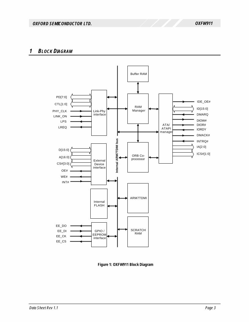
1 BLOCK DIAGRAM
Inte
rna
l A
RM
7T
DM
I b
us
ARM7TDMI
EE_DO
EE_DI GPIO /EEPROMinterfaceEE_CK
EE_CS
ATA/ATAPI
manager
IDE_OE#
IA[2:0]
ID[15:0]
DMARQ
DIOW#DIOR#IORDY
SCRATCHRAM
ORB Co-processor
RAMManager
Buffer RAM
D[15:0]
CS#[3:0]
A[16:0]
OE#
WE#
INT#
ExternalDevice
interface
Link-Phyinterface
PD[7:0]
CTL[1:0]
LINK_ON
LPS
LREQ
PHY_CLK
DMACK#
INTRQ#
ICS#[1:0]
InternalFLASH
Figure 1: OXFW911 Block Diagram

Data Sheet Rev 1.1 Page 4
OXFW911 OXFORD SEMICONDUCTOR LTD.
2 PIN INFORMATION
OXFW911-TQ-A
96
95
94
93
92
91
90
89
88
87
86
85
84
83
82
81
80
78
77
76
75
74
73
72
71
70
69
68
67
66
65
79
INTRQ
DM
AC
K#
VD
D
GN
DIO
RD
YD
IOR
#D
IOW
#D
MA
RQ
VD
DG
ND
ID1
5ID
0V
DD
GN
DID
14
ID1
ID1
3
ID1
2ID
3
GN
DID
11
ID4
ID1
0ID
5ID
9ID
6
GN
DID
8ID
7
ID2
IA1IA0IA2
ICS0#ICS1#
LINKONLPSPD7PD6
TES
T0TE
ST1
GPO1GPO2GPO3
VDDPD5PD4PD3PD2
GN
D
CKOUT
VDDPD1PD0
CTL1CTL0GND
PHYCLKVDD
LREQNC
GND
979899100101102103104105
124125126127128
107108109110111112113114115116117118119120121122123
106
646362616059585756
3736353433
5453525150494847464544434241403938
55
IRESETIDE_OE#
INT#A0VDD
UIF
TE
ST
_SE
L
A14A15A16WE#
A1A2A3A4A5A6
A7
VDDGND
A8A9A10A11A12
A13
GNDG
ND
GND
GPI
D1
5D
14
D1
3D
12
D1
1
D1
0
GN
D D9
D8
D7
D6
D5
D4
GN
DV
DD
D2
D1
D0
VD
D
RESET#
VD
D
CS3#CS2#
GN
D
VD
D
CS
1#
CS0#
OE
#
D3
1 2 3 4 5 6 7 8 9 10
11
12
13
14
15
16
17
19
20
21
22
23
24
25
26
27
28
29
30
31
32
18
NC
VDDGND
VD
DV
DD
VD
D
GN
D
Figure 2: Pinout (package = 128 TQFP)

Data Sheet Rev 1.1 Page 5
OXFW911 OXFORD SEMICONDUCTOR LTD.
3 PIN DESCRIPTIONS
Dir1 Name Description 1394 PHY-LINK interface 104, 105, 108, 109, 110, 111, 114,
115 I/O PD[7:0] Phy-Link Data Bus
116,117 I/O CTL[1:0] Phy-Link Control Bus 119 I PHYCLK 49.152 MHz clock sourced by PHY 121 O LREQ Link Request 102 IU LINKON Requests link to power up when in a low power mode 103 O LPS Indicates to phy that link is powered and ready
ARM external interface 2, 3, 4, 5, 6, 9, 10, 11, 12, 13, 16,
17, 18, 19, 20, 24 T_I/O D[15:0] ARM external data bus
35, 36, 37, 38, 41, 42, 43, 44, 45, 46, 49, 50, 51, 52, 53, 54, 60
T_O A[16:0] ARM external address bus
123, 124, 27, 33 T_O CS#[3:0] ARM external chip selects. CS0# is always used for program ROM.
28 T_O OE# ARM external output enable. Active when reading data from external devices including program ROM
34 T_O WE# Write Enable. Active when writing to external devices 61 T_IU INT# External ARM interrupt
IDE interface 86, 82, 80, 78, 74, 72, 70, 66, 65,
69, 71, 73, 77, 79, 81, 85 T_I/O ID[15:0] IDE data bus
99, 97, 98 T_O IA[2:0] IDE address bus 101, 100 T_O ICS#[1:0] IDE chip select. Used to select the Command Block or
Control Block registers. 63 T_O IDE_OE# IDE output enable. Only used when external buffering is
required to drive IDE data bus 64 T_O IRESET IDE interface reset 89 T_I DMARQ 90 T_O DIOW# IDE interface write strobe 91 T_O DIOR# IDE interface read strobe 92 T_O IORDY 95 T_O DMACK# 62 T_I INTRQ
EEPROM interface 125 O GPO1 General Purpose Output 1 126 O GPO2 General Purpose Output 2 127 O GPO3 General Purpose Output 3 58 T_IU GPI General Purpose Input
Miscellaneous Pins 56 IU RESET# Global reset for the OXFW911. Active Low.
128 T_O CKOUT Clock output. 49.152 MHz clock output. 22, 32, 31 I TEST_SEL,
TEST[1:0] ‘100’ = NORMAL OPERATION. Other settings are for foundry test purposes only.
57 IU UIF Leave unconnected to use internal Flash, tie low to use only external device
Power and ground2 15, 8, 40, 48, 59, 76, 94, 107, 113 VDD AC VDD Supplies power to output buffers in switching (AC) state
30, 21, 23, 68, 84, 88, 120 VDD DC VDD Power supply. Supplies power to core logic, input buffers and output buffers in steady state
Data Sheet Rev 1.1 Page 6
OXFW911 OXFORD SEMICONDUCTOR LTD.
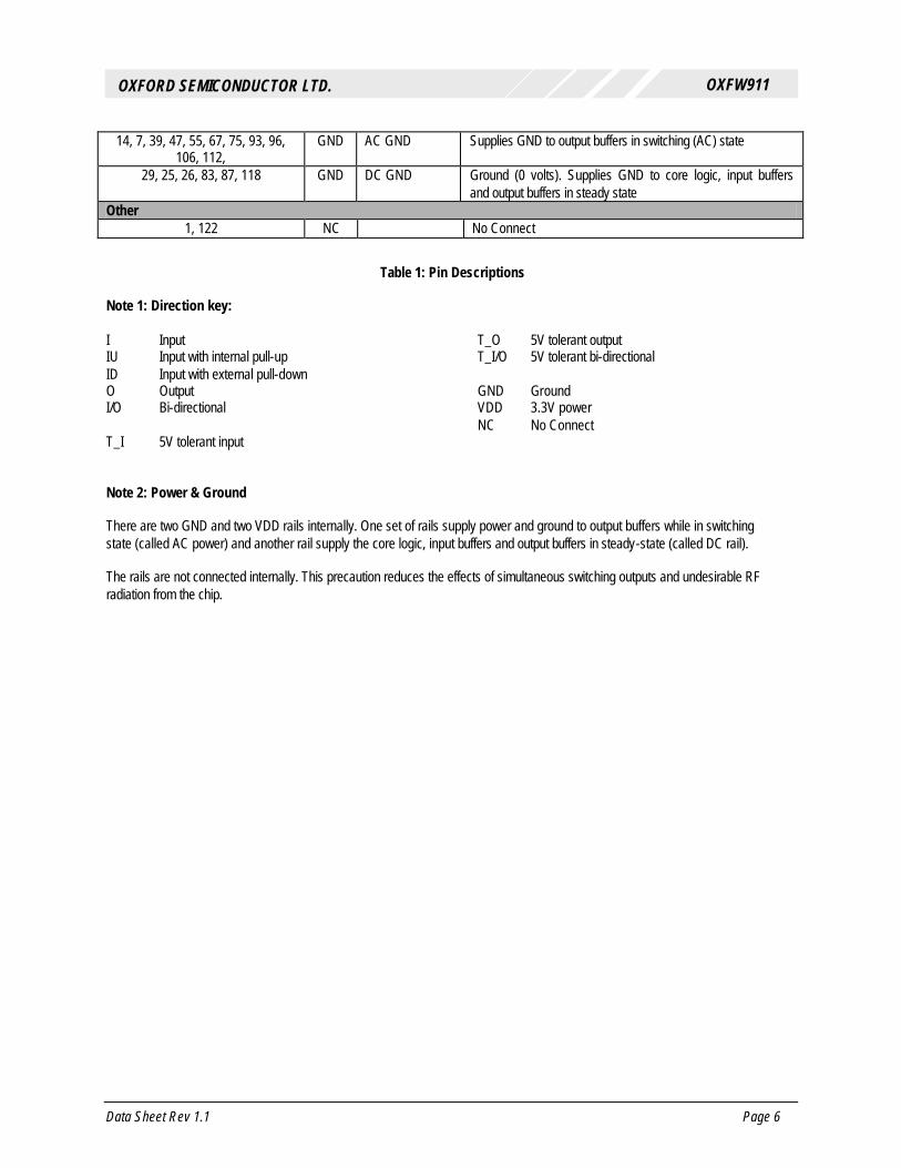
14, 7, 39, 47, 55, 67, 75, 93, 96, 106, 112,
GND AC GND Supplies GND to output buffers in switching (AC) state
29, 25, 26, 83, 87, 118 GND DC GND Ground (0 volts). Supplies GND to core logic, input buffers and output buffers in steady state
Other 1, 122 NC No Connect
Table 1: Pin Descriptions Note 1: Direction key: I Input IU Input with internal pull-up ID Input with external pull-down O Output I/O Bi-directional T_I 5V tolerant input
T_O 5V tolerant output T_I/O 5V tolerant bi-directional GND Ground VDD 3.3V power NC No Connect
Note 2: Power & Ground There are two GND and two VDD rails internally. One set of rails supply power and ground to output buffers while in switching state (called AC power) and another rail supply the core logic, input buffers and output buffers in steady-state (called DC rail). The rails are not connected internally. This precaution reduces the effects of simultaneous switching outputs and undesirable RF radiation from the chip.
Data Sheet Rev 1.1 Page 7
OXFW911 OXFORD SEMICONDUCTOR LTD.
Configuration & Operation
4 OPERATING CONDITIONS
Symbol Parameter Min Max Units
VDD DC supply voltage -0.3 3.8 V VIN DC input voltage (3.3V IO) -0.3 VDD + 0.3 V VIN DC input voltage (5V tolerant IO) -0.3 5.5 V IIN DC input current +/- 10 mA
TSTG Storage temperature -40 125 °C
Table 2: Absolute maximum ratings
Symbol Parameter Min Max Units VDD DC supply voltage 3.15 3.6 V TC Temperature 0 70 °C
Table 3: Recommended operating conditions
5 DC ELECTRICAL CHARACTERISTICS
5.1 I/O Buffers
Symbol Parameter Condition Min Max Units VDD Supply voltage Commercial 3.0 3.6 V VIH Input high voltage CMOS Interface
CMOS Schmitt trig 2.0 2.0
V
VIL Input low voltage CMOS Interface 1 CMOS Schmitt trig
0.8 0.8
V
CIL Cap of input buffers 4.0 pF COL Cap of output buffers 4.0 pF IIH Input high leakage current Vin = VDD -10 10 µA IIL Input low leakage current Vin = VSS -10 10 µA
VOH Output high voltage IOH = -1 µA VDD – 0.05 V VOH Output high voltage IOH = -1mA to –24mA 2.4 V VOL Output low voltage IOL = 1 µA 0.05 V VOL Output low voltage IOL = 1mA to 24mA 0.4 V IOZ 3-state output leakage current -10 10 µA
Symbol Parameter Condition Typical Max Units
VDD = 3.3V 85 TBD T=25°C
Operating supply current in normal mode
ICC Operating supply current in Power-down mode
mA
Table 4: Characteristics of OXFW911 I/O buffers

Data Sheet Rev 1.1 Page 8
OXFW911 OXFORD SEMICONDUCTOR LTD.
6 AC ELECTRICAL CHARACTERISTICS
6.1 IDE interface
Symbol Parameter Mode 0 Mode 1 Mode 2 Mode 3 Mode 4 Units t0 Cycle Time 600 400 360 200 120 ns t1 Address Valid to DIOR# / DIOW#
setup 80 80 40 40 40 ns
t2 DIOR# / DIOW# pulse width 320 320 320 80 80 ns t2i DIOR# / DIOW# recovery time - - - 80 40 ns t3 DIOW# data setup (min ) 60 45 30 30 20 ns t4 DIOW# data hold 40 40 40 40 40 ns t5 DIOR# data setup ( min ) 50 35 20 20 20 ns t6 DIOR# data hold ( min ) 5 5 5 5 5 ns
t6z DIOR# data tristate (max ) 30 30 30 30 30 ns t9 DIOR# / DIOW# to address valid
hold 40 40 40 40 40 ns
tRD Read Data Valid to IORDY active if IORDY initially low after tA
0 0 0 0 0 ns
tA IORDY Setup time 35 35 35 35 35 ns tB IORDY Pulse Width ( max ) 1250 1250 1250 1250 1250 ns tA IORDY assertion to release 5 5 5 5 5 ns
Table 5: OXFW911 IDE PIO / Register Transfers

Data Sheet Rev 1.1 Page 9
OXFW911 OXFORD SEMICONDUCTOR LTD.
Symbol Parameter Mode 0 Mode 1 Mode 2 Units
t0 Cycle time 480 160 120 ns tD DIOR# / DIOW# 240 80 80 ns tE DIOR# data access ( max ) 150 60 50 ns tF DIOR# data hold ( min ) 5 5 5 ns tG DIOR# / DIOW# data setup 100 30 20 ns tH DIOW# data hold 20 15 10 ns tI DMACK to DIOR# / DIOW# setup ( min ) 0 0 0 ns tJ DIOR# / DIOW# to DMACK hold ( min ) 20 5 5 ns
tKr DIOR# negated pulse width 80 80 40 ns tKw DIOW# negated pulse width 240 80 40 ns tLr DIOR# to DMARQ delay ( max ) 120 40 35 ns tLw DIOW# to DMARQ delay ( max ) 40 40 35 ns tM IDCS[1:0] valid to DIOR# / DIOW# 80 40 40 ns tN IDCS[1:0] hold 40 40 40 ns tZ DMACK to tristate ( max ) 20 25 25 ns
Table 6: OXFW911 Multiword DMA timings

Data Sheet Rev 1.1 Page 10
OXFW911 OXFORD SEMICONDUCTOR LTD.
Symbol Parameter Mode 0
min Mode 0
max Mode 1
min Mode1
max Mode 2
min Mode 2
max Units
t2cyc Typical sustained average two cycle time
240 160 120 ns
tcyc Cycle time allowing for clock variations ( refer to ATA spec)
112 75 55 ns
t2cyc Two cycle time allowing for clock variations ( refer to ATA spec )
230 156 117 ns
tds Data setup time at recipient 15 10 7 ns tdh Data hold time at recipient 5 5 5 ns
tdvs Data valid setup time at sender (from data bus being valid until STROBE edge )
70 48 34 ns
tdvh Data valid hold time at sender (from STROBE edge until data may become invalid
6 6 6 ns
tfs First STROBE time (for device to first negate DSTROBE from STOP during a data-in burst)
0 230 0 200 0 170 ns
tli Limited interlock time 0 150 0 150 0 150 ns tmli Interlock time with minimum 20 20 20 ns tui Unlimited interlock time 0 0 0 ns taz Maximum time allowed for output
drivers to release (from being asserted or negated)
10 10 10 ns
tzah tzad
Minimum delay time required for output drivers to assert or negate (from released state)
20 0
20 0
20 0
ns
tenv Envelope time ( from DMACK# to STOP and HDMARDY# during data-out burst initiation
20 70 20 70 20 70 ns
tsr STROBE to DMARDY time ( refer to ATA spec
50 30 20 ns
trfs Ready-to-final-STROBE time ( no STROBE edges shall be sent this long after the negation of DDMARDY#
75 70 60 ns
trp Ready-to-pause time ( time that recipient shall wait to initiate pause after negating DMARDY# )
160 125 100 ns
tiordyz Pull-up time before allowing IORDY to be released
20 20 20 ns
tziordy Minimum time a device shall wait before driving IORDY
0 0 0 ns
tack Setup and hold times for DMACK# (before assertion or negation )
20 20 20 ns
tss Time from STROBE edge to negation of DMARQ or assertion of STOP (when sender terminates a burst )
50 50 50 ns
Table 7: OXFW911 Ultra DMA timings
Data Sheet Rev 1.1 Page 11
OXFW911 OXFORD SEMICONDUCTOR LTD.
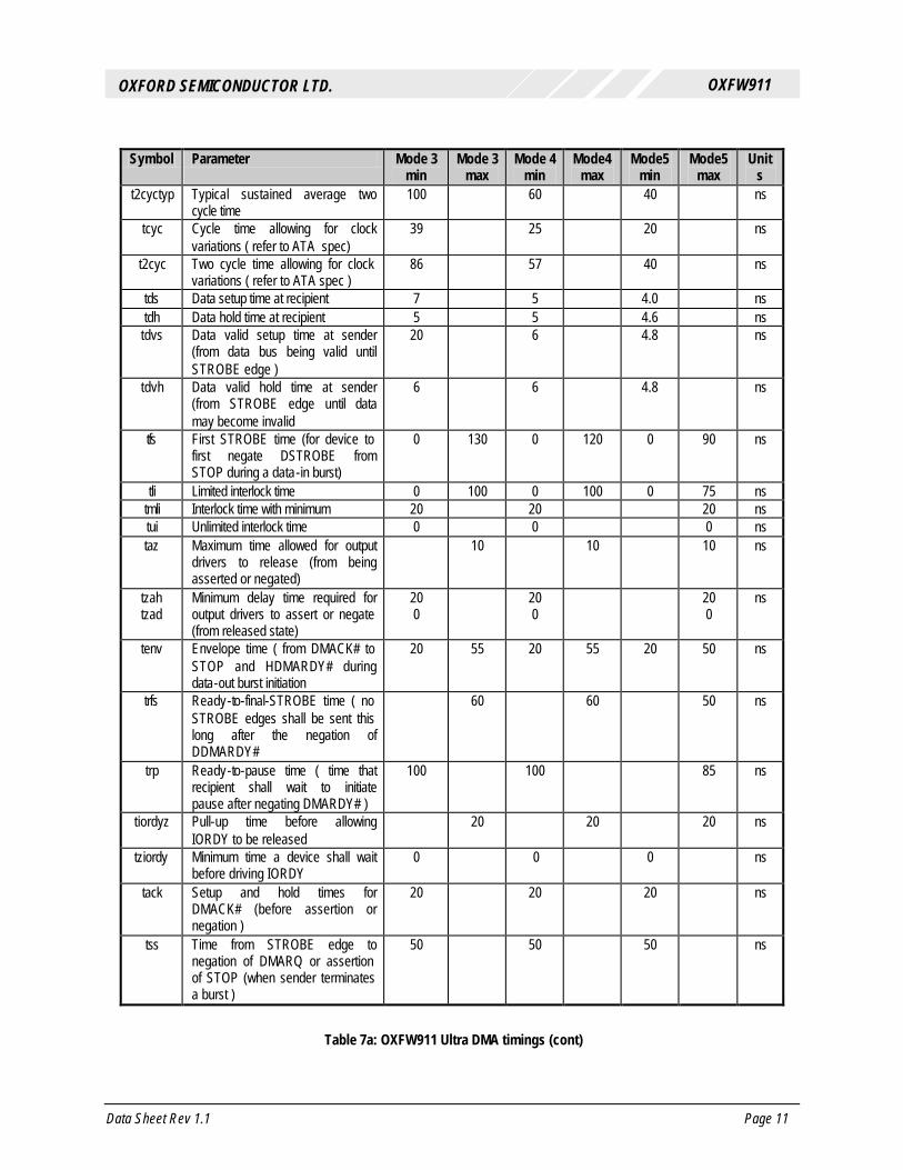
Symbol Parameter Mode 3
min Mode 3
max Mode 4
min Mode4
max Mode5
min Mode5
max Unit
s t2cyctyp Typical sustained average two
cycle time 100 60 40 ns
tcyc Cycle time allowing for clock variations ( refer to ATA spec)
39 25 20 ns
t2cyc Two cycle time allowing for clock variations ( refer to ATA spec )
86 57 40 ns
tds Data setup time at recipient 7 5 4.0 ns tdh Data hold time at recipient 5 5 4.6 ns
tdvs Data valid setup time at sender (from data bus being valid until STROBE edge )
20 6 4.8 ns
tdvh Data valid hold time at sender (from STROBE edge until data may become invalid
6 6 4.8 ns
tfs First STROBE time (for device to first negate DSTROBE from STOP during a data-in burst)
0 130 0 120 0 90 ns
tli Limited interlock time 0 100 0 100 0 75 ns tmli Interlock time with minimum 20 20 20 ns tui Unlimited interlock time 0 0 0 ns taz Maximum time allowed for output
drivers to release (from being asserted or negated)
10 10 10 ns
tzah tzad
Minimum delay time required for output drivers to assert or negate (from released state)
20 0
20 0
20 0
ns
tenv Envelope time ( from DMACK# to STOP and HDMARDY# during data-out burst initiation
20 55 20 55 20 50 ns
trfs Ready-to-final-STROBE time ( no STROBE edges shall be sent this long after the negation of DDMARDY#
60 60 50 ns
trp Ready-to-pause time ( time that recipient shall wait to initiate pause after negating DMARDY# )
100 100 85 ns
tiordyz Pull-up time before allowing IORDY to be released
20 20 20 ns
tziordy Minimum time a device shall wait before driving IORDY
0 0 0 ns
tack Setup and hold times for DMACK# (before assertion or negation )
20 20 20 ns
tss Time from STROBE edge to negation of DMARQ or assertion of STOP (when sender terminates a burst )
50 50 50 ns
Table 7a: OXFW911 Ultra DMA timings (cont)
Data Sheet Rev 1.1 Page 12
OXFW911 OXFORD SEMICONDUCTOR LTD.
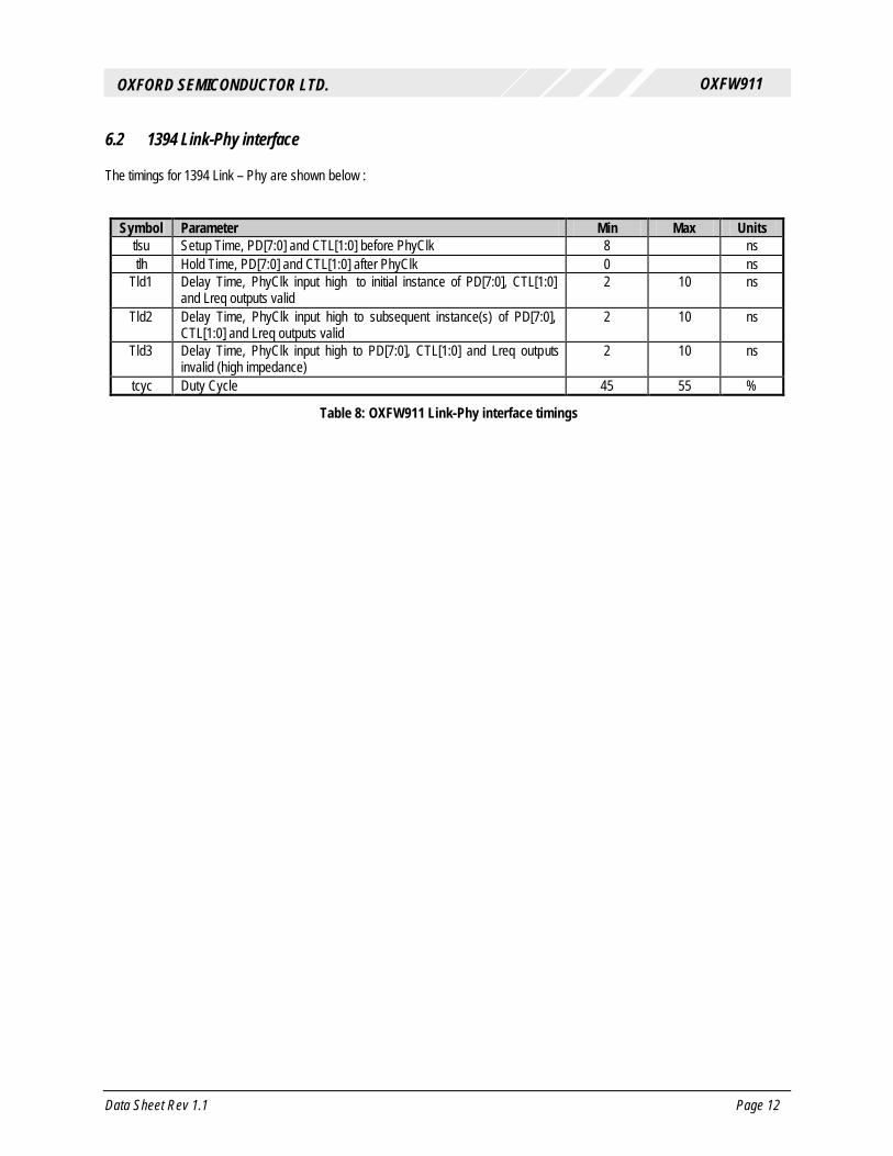
6.2 1394 Link-Phy interface
The timings for 1394 Link – Phy are shown below :
Symbol Parameter Min Max Units tlsu Setup Time, PD[7:0] and CTL[1:0] before PhyClk 8 ns tlh Hold Time, PD[7:0] and CTL[1:0] after PhyClk 0 ns
Tld1 Delay Time, PhyClk input high to initial instance of PD[7:0], CTL[1:0] and Lreq outputs valid
2 10 ns
Tld2 Delay Time, PhyClk input high to subsequent instance(s) of PD[7:0], CTL[1:0] and Lreq outputs valid
2 10 ns
Tld3 Delay Time, PhyClk input high to PD[7:0], CTL[1:0] and Lreq outputs invalid (high impedance)
2 10 ns
tcyc Duty Cycle 45 55 %
Table 8: OXFW911 Link-Phy interface timings
Data Sheet Rev 1.1 Page 13
OXFW911 OXFORD SEMICONDUCTOR LTD.
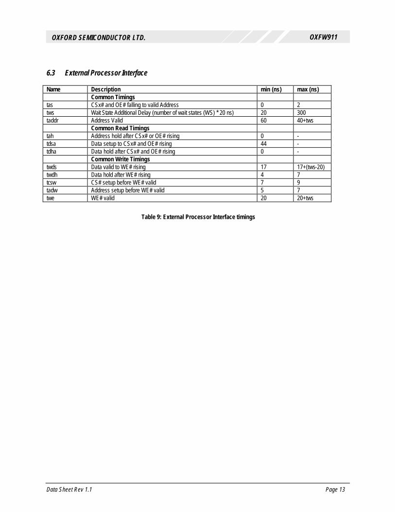
6.3 External Processor Interface
Name Description min (ns) max (ns) Common Timings tas CSx# and OE# falling to valid Address 0 2 tws Wait State Additional Delay (number of wait states (WS) * 20 ns) 20 300 taddr Address Valid 60 40+tws Common Read Timings tah Address hold after CSx# or OE# rising 0 - tdsa Data setup to CSx# and OE# rising 44 - tdha Data hold after CSx# and OE# rising 0 - Common Write Timings twds Data valid to WE# rising 17 17+(tws-20) twdh Data hold after WE# rising 4 7 tcsw CS# setup before WE# valid 7 9 tadw Address setup before WE# valid 5 7 twe WE# valid 20 20+tws
Table 9: External Processor Interface timings
Data Sheet Rev 1.1 Page 14
OXFW911 OXFORD SEMICONDUCTOR LTD.
7 TIMING WAVEFORMS
ADDR valid
DIOR# /DIOW#
ID[7:0](WRITE)
ID[7:0](READ)
IORDY(Note1)
t0
t1t2
t3 t4
t5t6
t6z
IORDY(Note2)
tA
IORDY(Note3)
tC
tRD
tBtC
t9
t2i
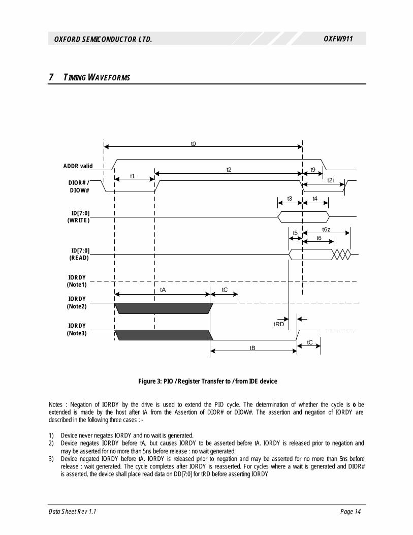
Figure 3: PIO / Register Transfer to / from IDE device Notes : Negation of IORDY by the drive is used to extend the PIO cycle. The determination of whether the cycle is to be extended is made by the host after tA from the Assertion of DIOR# or DIOW#. The assertion and negation of IORDY are described in the following three cases : - 1) Device never negates IORDY and no wait is generated. 2) Device negates IORDY before tA, but causes IORDY to be asserted before tA. IORDY is released prior to negation and
may be asserted for no more than 5ns before release : no wait generated. 3) Device negated IORDY before tA. IORDY is released prior to negation and may be asserted for no more than 5ns before
release : wait generated. The cycle completes after IORDY is reasserted. For cycles where a wait is generated and DIOR# is asserted, the device shall place read data on DD[7:0] for tRD before asserting IORDY

Data Sheet Rev 1.1 Page 15
OXFW911 OXFORD SEMICONDUCTOR LTD.
TIMING WAVEFORMS
CS0# / CS1#
DMARQ
DIOR# / DIOW#
DMACK#
tM tNt0
tL
tKtDtI tJ
tZ
READ ID[15:0]
tE
tG tF
tG tH
WRITE ID[15:0]
Figure 4: MultiWord DMA transfer to / from IDE device
Data Sheet Rev 1.1 Page 16
OXFW911 OXFORD SEMICONDUCTOR LTD.
DMARQ(device)
DMACK(host)
HDMARDY(host)(DIOR#)
STOP(host)(DIOW#)
DSTROBE(device)(IORDY)
ID[15:0]
IA[2:0], ICS#[1:0]
tui
tacktenv tfs
tzad
tziordy
taz
tack
tdvs tdvh
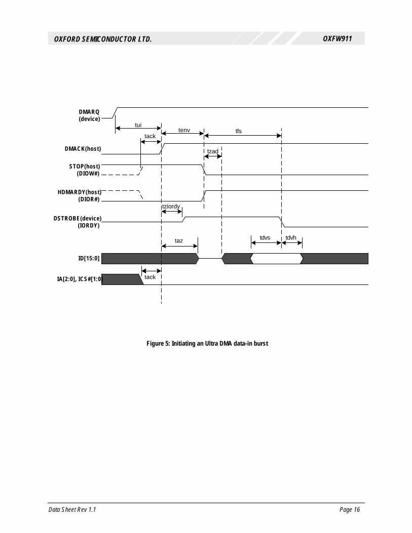
Figure 5: Initiating an Ultra DMA data-in burst

Data Sheet Rev 1.1 Page 17
OXFW911 OXFORD SEMICONDUCTOR LTD.
DSTROBE(device)(IORDY)
ID[15:0](device)
DSTROBE(host)IORDY
ID[15:0] (host)
t2cyc
tcyc tcyc
tdvh tdvs tdvh tdvs tdvh
tdhtds tdh tds tdh
Figure 6: Sustained Ultra DMA data-in burst

Data Sheet Rev 1.1 Page 18
OXFW911 OXFORD SEMICONDUCTOR LTD.
DMARQ(device)
DMACK(host)
STOP(host)DIOW#
ID[15:0] (host)
DSTROBE(device)IORDY
DSTROBE(device)IORDY
trp
tsr
trfs
Figure 7: Host pausing an Ultra DMA data-in burst

Data Sheet Rev 1.1 Page 19
OXFW911 OXFORD SEMICONDUCTOR LTD.
DMARQ(device)
DMACK(host)
STOP(host)DIOW#
ID[15:0] (host)
DSTROBE(device)IORDY
IA[2:0],ICS[1:0]
HDMARDY(host)DIOR#
tss
tli tli tmli
tack
tiordyz
tzahtaz
tack
CRC
Figure 8: Device terminating an Ultra DMA data-in burst

Data Sheet Rev 1.1 Page 20
OXFW911 OXFORD SEMICONDUCTOR LTD.
DMARQ(device)
DMACK(host)
STOP(host)DIOW#
ID[15:0] (host)
DSTROBE(device)IORDY
IA[2:0],ICS[1:0]
HDMARDY(host)DIOR#
tack
tiordyz
tack
CRC
trp
trfstli tmli
tzah
taz
tdvs tdvh
Figure 9: Host terminating an Ultra DMA data-in burst

Data Sheet Rev 1.1 Page 21
OXFW911 OXFORD SEMICONDUCTOR LTD.
DMARQ(device)
DMACK(host)
HSTROBE(host)(DIOR#)
STOP(host)(DIOW#)
DDMARDY(device)(IORDY)
ID[15:0]
IA[2:0], ICS#[1:0]
tui
tacktenv
tziordy
tack
tdvs tdvh
tli tui
Figure 10: Initiating an Ultra DMA data-out burst

Data Sheet Rev 1.1 Page 22
OXFW911 OXFORD SEMICONDUCTOR LTD.
HSTROBE(host)
ID[15:0] (host)
HSTROBE(device)
ID[15:0](device)
t2cyc
tcyc tcyc
tdvh tdvs tdvh tdvs tdvh
tdhtds tdh tds tdh
Figure 11: Sustained Ultra DMA data-out burst

Data Sheet Rev 1.1 Page 23
OXFW911 OXFORD SEMICONDUCTOR LTD.
DMARQ(device)
DMACK(host)
STOP(host)DIOW#
ID[15:0] (host)
DDMARDY(device)IORDY#
HSTROBE(host)DIOR#
trp
tsr
trfs
Figure 12: Device pausing an Ultra DMA data-in burst

Data Sheet Rev 1.1 Page 24
OXFW911 OXFORD SEMICONDUCTOR LTD.
DMARQ(device)
DMACK(host)
STOP(host)DIOW#
ID[15:0] (host)
HSTROBE(host)DIOR#
IA[2:0],ICS[1:0]
DDMARDY(device)IORDY#
tss
tli tli tmli
tack
tiordyz
tack
CRC
tdvs tdvh
Figure 13: Host Terminating an Ultra DMA data-out burst

Data Sheet Rev 1.1 Page 25
OXFW911 OXFORD SEMICONDUCTOR LTD.
DMARQ(device)
DMACK(host)
STOP(host)DIOW#
ID[15:0] (host)
HSTROBE(device)DIOR#
IA[2:0],ICS[1:0]
DDMARDY(device)IORDY#
tack
tiordyz
tack
CRC
trp
trfstli tmli
tli
tdvs tdvh
Figure 14: Device Terminating an Ultra DMA data-out burst

Data Sheet Rev 1.1 Page 26
OXFW911 OXFORD SEMICONDUCTOR LTD.
CLK1 2 3 4
PD[7:0]CTL[1:0]
LReq
tlsu tlh
tcyc
Figure 15: Phy to Link timings
CLK 12 3 4
PD[7:0]CTL[1:0]
LReqtld1 tld2 tld3
tcyc
Figure 16: Link to Phy timings

Data Sheet Rev 1.1 Page 27
OXFW911 OXFORD SEMICONDUCTOR LTD.
Address
Data
CS#
OE#
WE#
Address
Data
CS#
OE#
WE#
tws
tas
tdsa tdha
tah
taddr taddr
tdsa tdha tdsa tdhatas
tah
taddr
tws tws
Figure 17: External Processor Bus read timings

Data Sheet Rev 1.1 Page 28
OXFW911 OXFORD SEMICONDUCTOR LTD.
Address
Data
CS#
OE#
WE#
Address
Data
CS#
OE#
WE#
tws
tas
twds twdh
tah
taddr taddr
twds twdh twds twdhtas
tah
taddr
twe twe
tcsw
tadw
twe
Figure 17a: External Processor Bus write timings
Data Sheet Rev 1.1 Page 29
OXFW911 OXFORD SEMICONDUCTOR LTD.
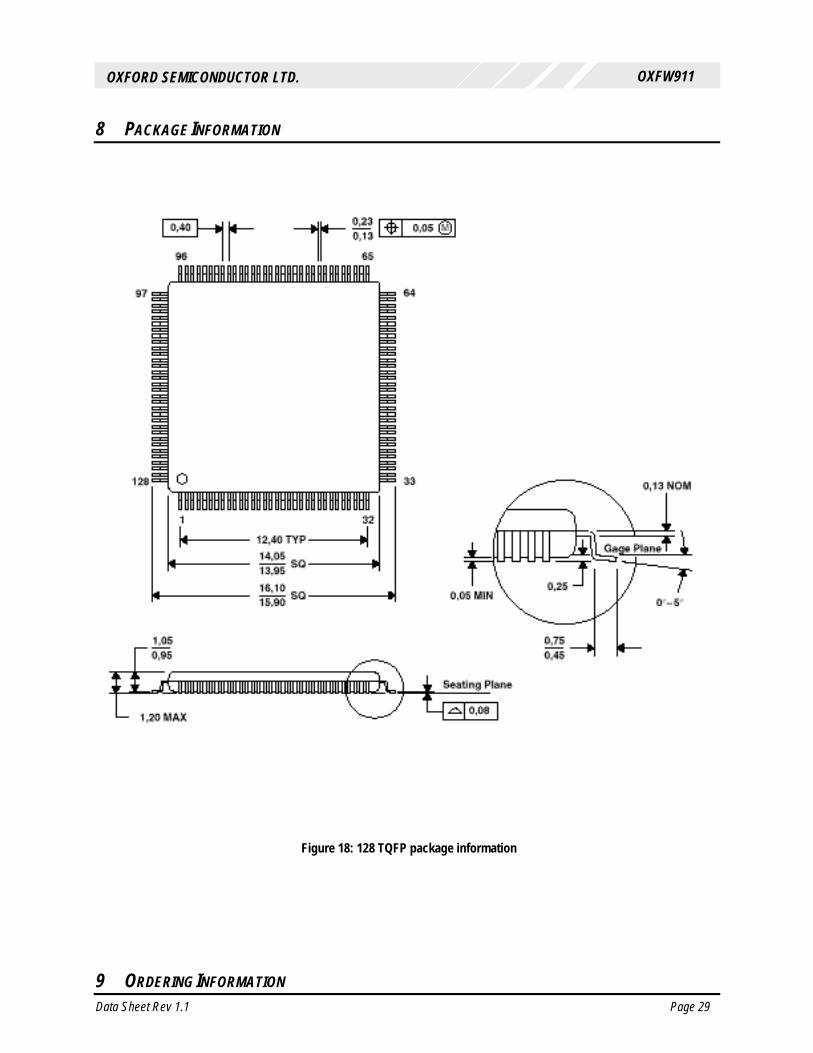
8 PACKAGE INFORMATION
Figure 18: 128 TQFP package information
9 ORDERING INFORMATION
Data Sheet Rev 1.1 Page 30
OXFW911 OXFORD SEMICONDUCTOR LTD.
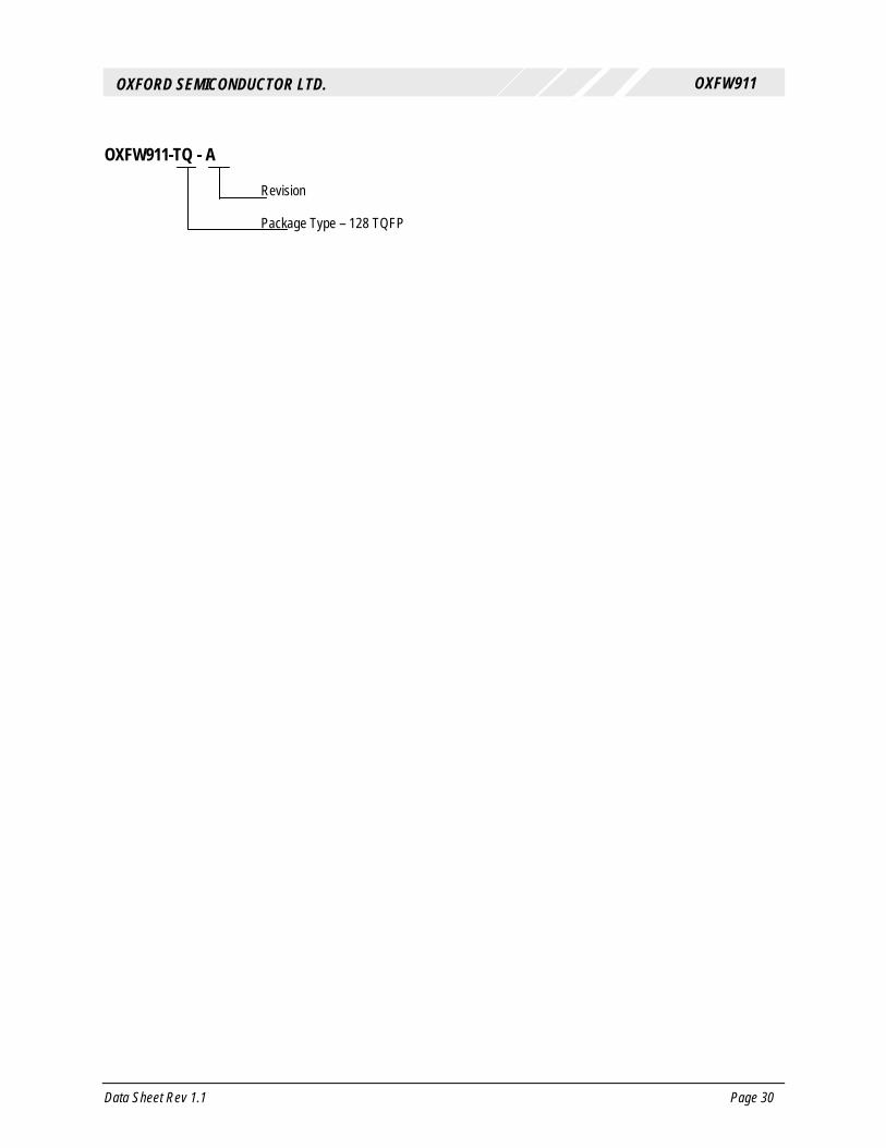
OXFW911-TQ - A Revision Package Type – 128 TQFP

Data Sheet Rev 1.1 Page 31
OXFW911 OXFORD SEMICONDUCTOR LTD.
NOTES
This page has been intentionally left blank

Data Sheet Rev 1.1 Page 32
OXFW911 OXFORD SEMICONDUCTOR LTD.
CONTACT DETAILS
Oxford Semiconductor Ltd. 25 Milton Park Abingdon Oxfordshire OX14 4SH United Kingdom Telephone: +44 (0)1235 824900 Fax: +44 (0)1235 821141 Sales e-mail: [email protected] Web site: http://www.oxsemi.com
DISCLAIMER
Oxford Semiconductor believes the information contained in this document to be accurate and reliable. However, it is subject to change without notice. No responsibility is assumed by Oxford Semiconductor for its use, nor for infringement of patents or other rights of third parties. No part of this publication may be reproduced, or transmitted in any form or by any means without the prior consent of Oxford Semiconductor Ltd. Oxford Semiconductor’s terms and conditions of sale apply at all times.