UNITUNIT- ---IIIIIIIIIIII COMBINATIONAL LOGIC DESIGN Decoders
58
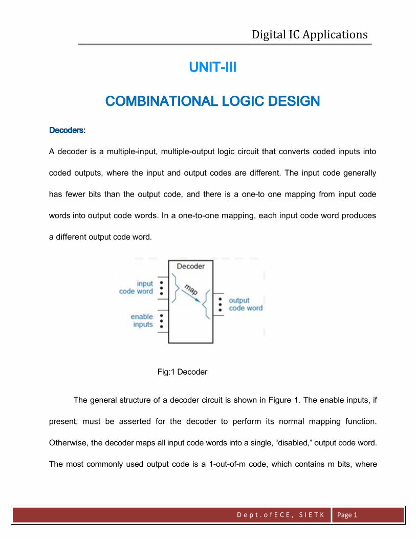
Digital IC Applications Dept.ofECE, SIETK Page 1 UNIT UNIT UNIT UNIT-III III III III COMBINATIONAL LOGIC DESIGN COMBINATIONAL LOGIC DESIGN COMBINATIONAL LOGIC DESIGN COMBINATIONAL LOGIC DESIGN Decoders: Decoders: Decoders: Decoders: A decoder is a multiple-input, multiple-output logic circuit that converts coded inputs into coded outputs, where the input and output codes are different. The input code generally has fewer bits than the output code, and there is a one-to one mapping from input code words into output code words. In a one-to-one mapping, each input code word produces a different output code word. Fig:1 Decoder The general structure of a decoder circuit is shown in Figure 1. The enable inputs, if present, must be asserted for the decoder to perform its normal mapping function. Otherwise, the decoder maps all input code words into a single, “disabled,” output code word. The most commonly used output code is a 1-out-of-m code, which contains m bits, where
Transcript of UNITUNIT- ---IIIIIIIIIIII COMBINATIONAL LOGIC DESIGN Decoders
Digital IC Applications
D e p t . o f E C E , S I E T K
Page 1
UNITUNITUNITUNIT----IIIIIIIIIIII
COMBINATIONAL LOGIC DESIGNCOMBINATIONAL LOGIC DESIGNCOMBINATIONAL LOGIC DESIGNCOMBINATIONAL LOGIC DESIGN
Decoders: Decoders: Decoders: Decoders:
A decoder is a multiple-input, multiple-output logic circuit that converts coded inputs into
coded outputs, where the input and output codes are different. The input code generally
has fewer bits than the output code, and there is a one-to one mapping from input code
words into output code words. In a one-to-one mapping, each input code word produces
a different output code word.
Fig:1 Decoder
The general structure of a decoder circuit is shown in Figure 1. The enable inputs, if
present, must be asserted for the decoder to perform its normal mapping function.
Otherwise, the decoder maps all input code words into a single, “disabled,” output code word.
The most commonly used output code is a 1-out-of-m code, which contains m bits, where

Digital IC Applications
D e p t . o f E C E , S I E T K
Page 2
one bit is asserted at any time. Thus, in a 1-out-of-4 code with active-high outputs, the
code words are 0001, 0010, 0100, and 1000. With active-low outputs, the code words are
1110, 1101, 1011, and 0111.
Binary Decoders Binary Decoders Binary Decoders Binary Decoders
The most common decoder circuit is an n-to-2n decoder or binary decoder. Such a decoder
has an n-bit binary input code and a 1-out-of-2n output code. A binary decoder is used when
you need to activate exactly one of 2n outputs based on an n-bit input value
Table 1 is the truth table of a 2-to-4 decoder. The input code word 1,I0 represents an integer
in the range 0-3. The output code word Y3,Y2,Y1,Y0 has Yi equal to 1 if and only if the
input code word is the binary representation of i and the enable input EN is 1. If EN is 0, then
all of the outputs are 0. A gate-level circuit for the 2-to-4 decoder is shown in Figure 2 Each
AND gate decodes one combination of the input code word I1,I0.
Digital IC Applications
D e p t . o f E C E , S I E T K
Page 3
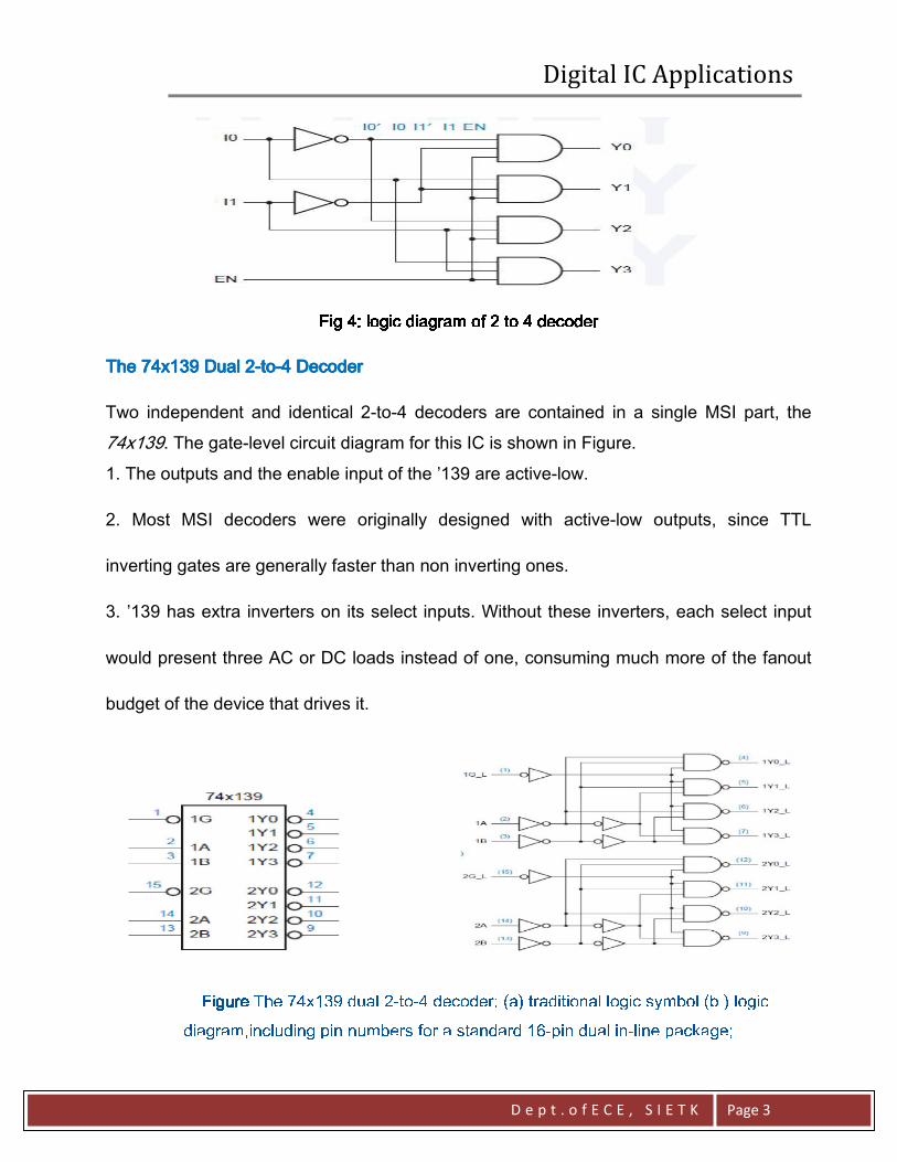
Fig 4: logic diagram of 2 to 4 decoder
Fig 4: logic diagram of 2 to 4 decoderFig 4: logic diagram of 2 to 4 decoder
Fig 4: logic diagram of 2 to 4 decoder
The 74x139 Dual 2The 74x139 Dual 2The 74x139 Dual 2The 74x139 Dual 2----totototo----4 Decoder4 Decoder4 Decoder4 Decoder
Two independent and identical 2-to-4 decoders are contained in a single MSI part, the
74x139. The gate-level circuit diagram for this IC is shown in Figure.
1. The outputs and the enable input of the ’139 are active-low.
2. Most MSI decoders were originally designed with active-low outputs, since TTL
inverting gates are generally faster than non inverting ones.
3. ’139 has extra inverters on its select inputs. Without these inverters, each select input
would present three AC or DC loads instead of one, consuming much more of the fanout
budget of the device that drives it.
Figure
Figure Figure
Figure The 74x139 dual 2-to-4 decoder: (a) traditional logic symbol (b ) logic
diagram,including pin numbers for a standard 16-pin dual in-line package;

Digital IC Applications
D e p t . o f E C E , S I E T K
Page 4
In this case, the assignment of the generic function to one half or the other of a
particular ’139 package can be deferred until the schematic is completed Table is the truth
table for a 74x139-type decoder.
The 74x138 3The 74x138 3The 74x138 3The 74x138 3----totototo----8 Decoder8 Decoder8 Decoder8 Decoder
The 74x138 is a commercially available MSI 3-to-8 decoder whose gate-level circuit diagram
and symbol are shown in Figure 7; its truth table is given in Table. Like the 74x139, the
74x138 has active-low outputs, and it has three enable inputs (G1, /G2A, /G2B), all of which
must be asserted for the selected output to be asserted.

Digital IC Applications
D e p t . o f E C E , S I E T K
Page 5
However, because of the inversion bubbles, we have the following relations between internal
and external signals:
Therefore, if we’re interested, we can write the following equation for the external output signal
Y5_L in terms of external input signals:
On the surface, this equation doesn’t resemble what you might expect for a decoder, since
it is a logical sum rather than a product. However, if you practice bubble-to-bubble logic
design, you don’t have to worry about this; you just give the output signal an active-low
name and remember that it’s active low when you connect it to other inputs.
Cascading Binary DecodersCascading Binary DecodersCascading Binary DecodersCascading Binary Decoders
Multiple binary decoders can be used to decode larger code words. Figure 5-38 shows
how two 3-to-8 decoders can be combined to make a 4-to-16 decoder. The availability of
both active-high and active-low enable inputs on the 74x138 makes it possible to enable
one or the other directly based on the state of the most significant input bit. The top
decoder (U1) is enabled when N3 is 0, and the bottom one (U2) is enabled when N3 is 1.

Digital IC Applications
D e p t . o f E C E , S I E T K
Page 6
Figure
FigureFigure
Figure
Design of a 4-to-16 decoder using 74x138s.

Digital IC Applications
D e p t . o f E C E , S I E T K
Page 7

Digital IC Applications
D e p t . o f E C E , S I E T K
Page 8
SevenSevenSevenSeven----Segment DecodersSegment DecodersSegment DecodersSegment Decoders
Look at your wrist and you’ll probably see a seven-segment display. This type of display,
which normally uses light-emitting diodes (LEDs) or liquid-crystal display (LCD) elements,
is used in watches, calculators, and instruments to display decimal data. A digit is
displayed by illuminating a subset of the seven line segments shown in Figure (a). A
seven-segment decoder has 4-bit BCD as its input code and the “sevensegment code,”

Digital IC Applications
D e p t . o f E C E , S I E T K
Page 9
Figure
Figure Figure
Figure The 74x49 seven-segment decoder: (a) traditional logic symbol (b) logic diagram,
including pin numbers

Digital IC Applications
D e p t . o f E C E , S I E T K
Page 10
EncodersEncodersEncodersEncoders
A decoder’s output code normally has more bits than its input code. If the device’s output
code has fewer bits than the input code, the device is usually called an encoder. Probably
the simplest encoder to build is a 2n-to-n or binary encoder. As shown in Figure(a), it has
just the opposite function as a binary decoder— its input code is the 1-out-of-2n code and
its output code is n-bit binary. The equations for an 8-to-3 encoder with inputs I0–I7 and
outputs Y0–Y2 are given below:
The corresponding logic circuit is shown in (b). In general, a 2n-to-n encoder can be built
from n 2n1-input OR gates. Bit i of the input code is connected to OR gate j if bit j in the
binary representation of i is 1.
Priority EncodersPriority EncodersPriority EncodersPriority Encoders
The 1-out-of-2n coded outputs of an n-bit binary decoder are generally used to control a
set of 2n devices, where at most one device is supposed to be active at any time.
Conversely, consider a system with 2n inputs, each of which indicates a request for

Digital IC Applications
D e p t . o f E C E , S I E T K
Page 11
service. This structure is often found in microprocessor input/output subsystems, where
the inputs might be interrupt requests. In this situation, it may seem natural to use a binary
encoder. to observe the inputs and indicate which one is requesting service at any time.
However, this encoder works properly only if the inputs are guaranteed to be asserted at
most one at a time. If multiple requests can be made simultaneously, the encoder gives
undesirable results. For example, suppose that inputs I2 and I4 of the 8-to-3 encoder are
both 1; then the output is 110, the binary encoding of 6.
Y0 = I1 + I3 + I5 + I7
Y1 = I2 + I3 + I6 + I7
Y2 = I4 + I5 + I6 + I7
Either 2 or 4, not 6, would be a useful output in the preceding example, but how can the
encoding device decide which? The solution is to assign priority to the input lines, so that
when multiple requests are asserted, the encoding device produces the number of the
highest-priority requestor. Such a device is called a priority encoder.
Input I7 has the highest priority. Outputs A2–A0 contain the number of the highest-
priority asserted input, if any. The IDLE output is asserted if no inputs are asserted. In
order to write logic equations for the priority encoder’s outputs, we first define eight
intermediate variables H0–H7, such that Hi is 1 if and only if Ii is the highest priority 1
input: Using these signals, the equations for the A2–A0 outputs are similar to the ones for
a simple binary encoder:

Digital IC Applications
D e p t . o f E C E , S I E T K
Page 12
H7=I7 (Highest Priority)
H7=I7 (Highest Priority)H7=I7 (Highest Priority)
H7=I7 (Highest Priority)
H6=I6.I7’
H6=I6.I7’H6=I6.I7’
H6=I6.I7’
H5=I5.I6’.I7’
H5=I5.I6’.I7’H5=I5.I6’.I7’
H5=I5.I6’.I7’
H4=I4.I5’.I6’.I7’
H4=I4.I5’.I6’.I7’H4=I4.I5’.I6’.I7’
H4=I4.I5’.I6’.I7’
H3=I3.I4’.I5’.I6’.I7’
H3=I3.I4’.I5’.I6’.I7’H3=I3.I4’.I5’.I6’.I7’
H3=I3.I4’.I5’.I6’.I7’
H
HH
H2=I2.I3’.I4’.I5’.I6’.I7’
2=I2.I3’.I4’.I5’.I6’.I7’2=I2.I3’.I4’.I5’.I6’.I7’
2=I2.I3’.I4’.I5’.I6’.I7’
H1=I1. I2’.I3’.I4’.I5’.I6’.I7’
H1=I1. I2’.I3’.I4’.I5’.I6’.I7’H1=I1. I2’.I3’.I4’.I5’.I6’.I7’
H1=I1. I2’.I3’.I4’.I5’.I6’.I7’
H0=I0.I1’. I2’.I3’.I4’.I5’.I6’.I7’
H0=I0.I1’. I2’.I3’.I4’.I5’.I6’.I7’H0=I0.I1’. I2’.I3’.I4’.I5’.I6’.I7’
H0=I0.I1’. I2’.I3’.I4’.I5’.I6’.I7’
IDLE= I0’.I1’. I2’.I3’.I4’.I5’.I6’.I7’
IDLE= I0’.I1’. I2’.I3’.I4’.I5’.I6’.I7’IDLE= I0’.I1’. I2’.I3’.I4’.I5’.I6’.I7’
IDLE= I0’.I1’. I2’.I3’.I4’.I5’.I6’.I7’
-
--
-
Encoder
EncoderEncoder
Encoder
A0=Y0 = H1 + H3 + H5 + H7
A0=Y0 = H1 + H3 + H5 + H7A0=Y0 = H1 + H3 + H5 + H7
A0=Y0 = H1 + H3 + H5 + H7
A1=Y1 = H2 + H3 + H6 + H7
A1=Y1 = H2 + H3 + H6 + H7A1=Y1 = H2 + H3 + H6 + H7
A1=Y1 = H2 + H3 + H6 + H7
A2=Y2 = H4 + H5 + H6 + H7
A2=Y2 = H4 + H5 + H6 + H7A2=Y2 = H4 + H5 + H6 + H7
A2=Y2 = H4 + H5 + H6 + H7
8-input priority encoder
I7 has the highest priority,I0 least
A2-A0 contain the number of the highest-priority asserted input if any.
IDLE is asserted if no inputs are asserted.

Digital IC Applications
D e p t . o f E C E , S I E T K
Page 13
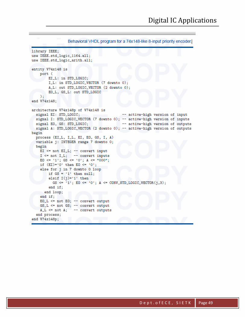
The 74x148 Priority EncoderThe 74x148 Priority EncoderThe 74x148 Priority EncoderThe 74x148 Priority Encoder
The 74x148 is a commercially available, MSI 8-input priority encoder it has an enable
input, EI_L, that must be asserted for any of its outputs to be asserted. The complete truth
table is given in Table. Instead of an IDLE output, the ’148 has a GS_L output that is
asserted when the device is enabled and one or more of the request inputs is asserted.
The manufacturer calls this “Group Select,” but it’s easier to remember as “Got
Something.” The EO_L signal is an enable output designed to be connected to the EI_L
input of another ’148 that handles lower-priority requests. EO is asserted if EI_L is
asserted but no request input is asserted; thus, a lower-priority ’148 may be enabled
Figure shows how four 74x148s can be connected in this way to accept 32 request
inputs and produce a 5-bit output, RA4–RA0, indicating the highest-priority requestor.
Since the A2–A0 outputs of at most one ’148 will be enabled at any time, the outputs of
Digital IC Applications
D e p t . o f E C E , S I E T K
Page 14
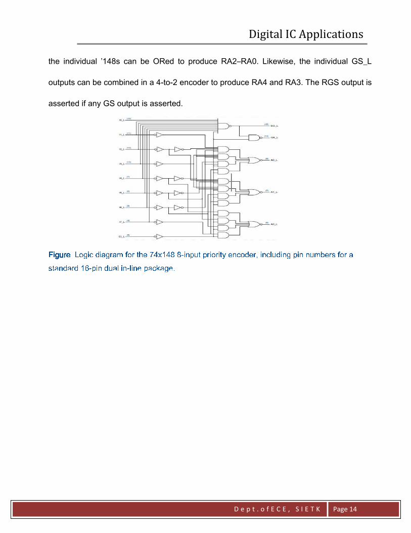
the individual ’148s can be ORed to produce RA2–RA0. Likewise, the individual GS_L
outputs can be combined in a 4-to-2 encoder to produce RA4 and RA3. The RGS output is
asserted if any GS output is asserted.
Figure
Figure Figure
Figure Logic diagram for the 74x148 8-input priority encoder, including pin numbers for a
standard 16-pin dual in-line package.

Digital IC Applications
D e p t . o f E C E , S I E T K
Page 15
Figure
Figure Figure
Figure Four 74x148s cascaded to handle 32 requests.
ThreeThreeThreeThree----State Devices:State Devices:State Devices:State Devices:
ThreeThreeThreeThree----State BuffersState BuffersState BuffersState Buffers
The most basic three-state device is a three-state buffer, often called a three-state driver.
The logic symbols for four physically different three-state buffers are shown in Figure

Digital IC Applications
D e p t . o f E C E , S I E T K
Page 16
The basic symbol is that of a noninverting buffer (a, b) or an inverter (c, d). The extra
signal at the top of the symbol is a three-state enable input, which may be active high (a,
c) or active low (b, d). When the enable input is asserted, the device behaves like an
ordinary buffer or inverter. When the enable input is negated, the device output “floats”;
that is, it goes to a high impedance (Hi-Z), disconnected state and functionally behaves as
if it weren’t even there.
Both enable inputs, G1_L and G2_L, must be asserted to enable the device’s three-
state outputs. The little rectangular symbols inside the buffer symbols indicate hysteresis,
an electrical characteristic of the inputs that improves noise immunity. The 74x541 inputs
typically have 0.4 volts of hysteresis.
Figure shows part of a microprocessor system with an 8-bit data bus, DB[0–7], and
a 74x541 used as an input port. The microprocessor selects Input Port 1 by asserting

Digital IC Applications
D e p t . o f E C E , S I E T K
Page 17
INSEL1 and requests a read operation by asserting READ. The selected 74x541 responds
by driving the microprocessor data bus with user supplied input data. Other input ports
may be selected when a different INSEL line is asserted along with READ.
A bus transceiver is typically used between two bidirectional buses, as shown in Figure.
Three different modes of operation are possible, depending on the state of G_L and DIR,
as shown in Table. As usual, it is the designer’s responsibility to ensure that neither bus is
ever driven simultaneously by two devices. However, independent transfers where both
buses are driven at the same time may occur when the transceiver is disabled, as
indicated in the last row of the table.
Digital IC Applications
D e p t . o f E C E , S I E T K
Page 18
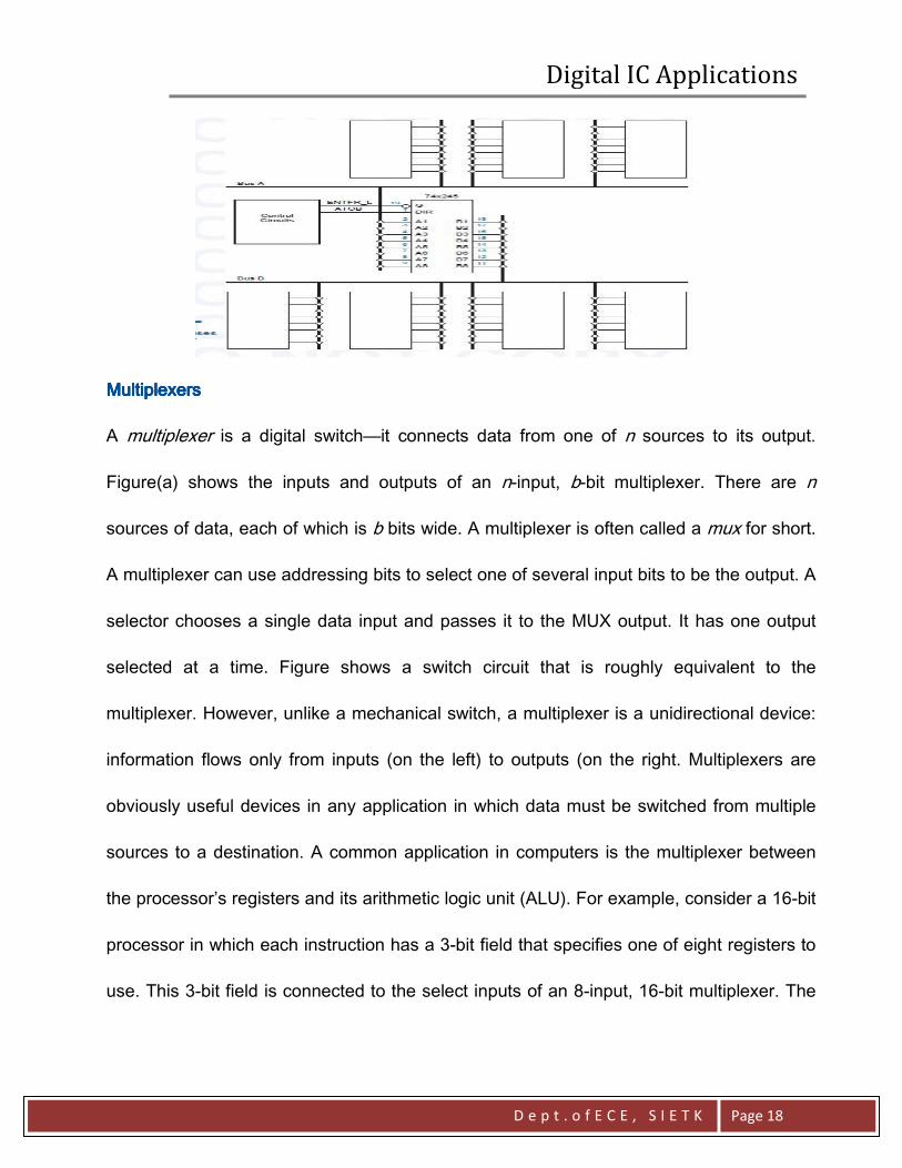
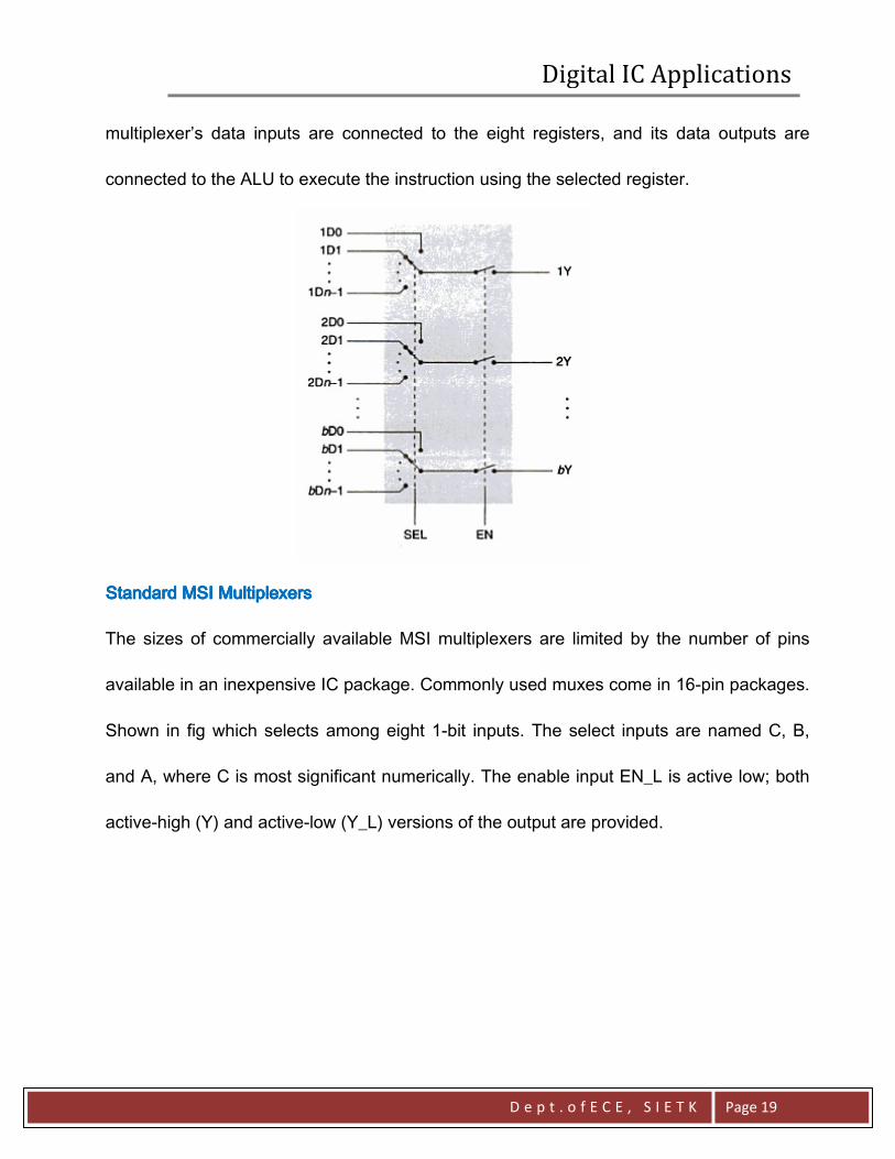
MultiplexersMultiplexersMultiplexersMultiplexers
A multiplexer is a digital switch—it connects data from one of n sources to its output.
Figure(a) shows the inputs and outputs of an n-input, b-bit multiplexer. There are n
sources of data, each of which is b bits wide. A multiplexer is often called a mux for short.
A multiplexer can use addressing bits to select one of several input bits to be the output. A
selector chooses a single data input and passes it to the MUX output. It has one output
selected at a time. Figure shows a switch circuit that is roughly equivalent to the
multiplexer. However, unlike a mechanical switch, a multiplexer is a unidirectional device:
information flows only from inputs (on the left) to outputs (on the right. Multiplexers are
obviously useful devices in any application in which data must be switched from multiple
sources to a destination. A common application in computers is the multiplexer between
the processor’s registers and its arithmetic logic unit (ALU). For example, consider a 16-bit
processor in which each instruction has a 3-bit field that specifies one of eight registers to
use. This 3-bit field is connected to the select inputs of an 8-input, 16-bit multiplexer. The
Digital IC Applications
D e p t . o f E C E , S I E T K
Page 19
multiplexer’s data inputs are connected to the eight registers, and its data outputs are
connected to the ALU to execute the instruction using the selected register.
Standard MSI MultiplexersStandard MSI MultiplexersStandard MSI MultiplexersStandard MSI Multiplexers
The sizes of commercially available MSI multiplexers are limited by the number of pins
available in an inexpensive IC package. Commonly used muxes come in 16-pin packages.
Shown in fig which selects among eight 1-bit inputs. The select inputs are named C, B,
and A, where C is most significant numerically. The enable input EN_L is active low; both
active-high (Y) and active-low (Y_L) versions of the output are provided.

Digital IC Applications
D e p t . o f E C E , S I E T K
Page 20
Figure
Figure Figure
Figure The 74x151 8-input, 1-bit multiplexer: (a) logic diagram, including pin numbers for a standard 16-pin
dual in-line package; (b) traditional logic symbol.
At the other extreme of muxes in 16-pin packages, we have the 74x157, shown in
Figure, which selects between two 4-bit inputs. Just to confuse things, the manufacturer
has named the select input S and the active-low enable input G_L. Also note that the data
sources are named A and B .
Digital IC Applications
D e p t . o f E C E , S I E T K
Page 21
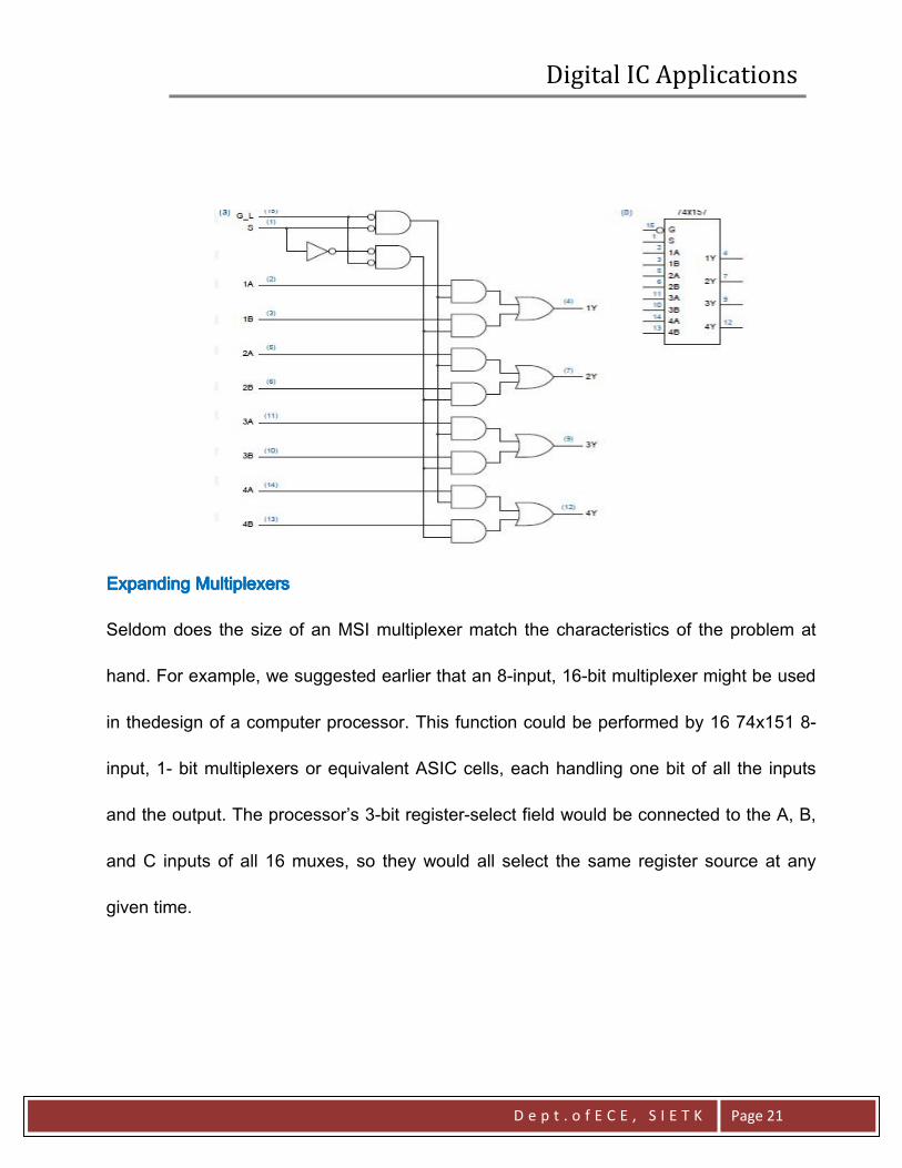
Expanding MultiplexersExpanding MultiplexersExpanding MultiplexersExpanding Multiplexers
Seldom does the size of an MSI multiplexer match the characteristics of the problem at
hand. For example, we suggested earlier that an 8-input, 16-bit multiplexer might be used
in thedesign of a computer processor. This function could be performed by 16 74x151 8-
input, 1- bit multiplexers or equivalent ASIC cells, each handling one bit of all the inputs
and the output. The processor’s 3-bit register-select field would be connected to the A, B,
and C inputs of all 16 muxes, so they would all select the same register source at any
given time.

Digital IC Applications
D e p t . o f E C E , S I E T K
Page 22
Another dimension in which multiplexers can be expanded is the number of data sources.
For example, suppose we needed a 32-input, 1-bit multiplexer. Figure shows one way to
build it. Five select bits are required. A 2-to-4 decoder (one-half of a 74x139) decodes the
two highorder select bits to enable one of four 74x151 8-input multiplexers. Since only one
’151 is enabled at a time, the ’151 outputs can simply be ORed to obtain the final output.
The 32-to-1 multiplexer can also be built using 74x251s. The circuit is identical to Figure,
except that the output NAND gate is eliminated. Instead, the Y (and, if desired, Y_L)
outputs of the four ’251s are simply tied together. The ’139 decoder ensures that at most
one of the ’251s has its threestate outputs enabled at any time. If the ’139 is disabled
(XEN_L is negated), then all of the ’251s are disabled, and the XOUT and XOUT_L
outputs are undefined. However, if desired, resistors may be connected from each of
these signals to 5 volts to pull the output HIGH in this case.
Digital IC Applications
D e p t . o f E C E , S I E T K
Page 23
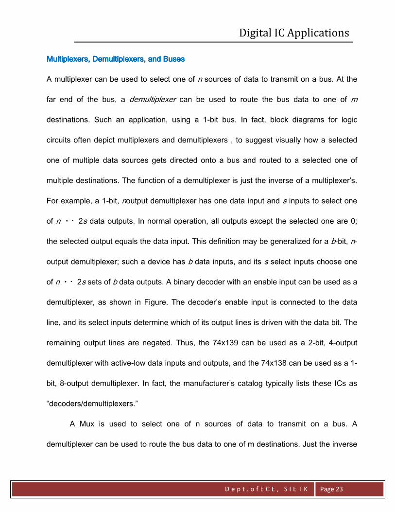
Multiplexers, Demultiplexers, and BusesMultiplexers, Demultiplexers, and BusesMultiplexers, Demultiplexers, and BusesMultiplexers, Demultiplexers, and Buses
A multiplexer can be used to select one of n sources of data to transmit on a bus. At the
far end of the bus, a demultiplexer can be used to route the bus data to one of m
destinations. Such an application, using a 1-bit bus. In fact, block diagrams for logic
circuits often depict multiplexers and demultiplexers , to suggest visually how a selected
one of multiple data sources gets directed onto a bus and routed to a selected one of
multiple destinations. The function of a demultiplexer is just the inverse of a multiplexer’s.
For example, a 1-bit, noutput demultiplexer has one data input and s inputs to select one
of n �2s data outputs. In normal operation, all outputs except the selected one are 0;
the selected output equals the data input. This definition may be generalized for a b-bit, n-
output demultiplexer; such a device has b data inputs, and its s select inputs choose one
of n �2s sets of b data outputs. A binary decoder with an enable input can be used as a
demultiplexer, as shown in Figure. The decoder’s enable input is connected to the data
line, and its select inputs determine which of its output lines is driven with the data bit. The
remaining output lines are negated. Thus, the 74x139 can be used as a 2-bit, 4-output
demultiplexer with active-low data inputs and outputs, and the 74x138 can be used as a 1-
bit, 8-output demultiplexer. In fact, the manufacturer’s catalog typically lists these ICs as
“decoders/demultiplexers.”
A Mux is used to select one of n sources of data to transmit on a bus. A
demultiplexer can be used to route the bus data to one of m destinations. Just the inverse
Digital IC Applications
D e p t . o f E C E , S I E T K
Page 24
of a mux. A binary decoder with an enable input can be used as a Demux. E.g. 74x139
can be used as a 2-bit, 4- output Demux.
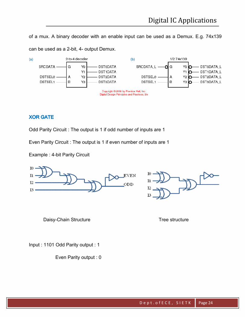
XOR GATEXOR GATEXOR GATEXOR GATE
Odd Parity Circuit : The output is 1 if odd number of inputs are 1
Even Parity Circuit : The output is 1 if even number of inputs are 1
Example : 4-bit Parity Circuit
Daisy-Chain Structure Tree structure
Input : 1101 Odd Parity output : 1
Even Parity output : 0

Digital IC Applications
D e p t . o f E C E , S I E T K
Page 25
Four XOR gates are provided in a single 14-pin SSI IC, the 74x86 shown in Figure. New
SSI logic families do not offer XNOR gates, although they are readily available in FPGA
and ASIC libraries and as primitives in HDLs.
Parity CircuitsParity CircuitsParity CircuitsParity Circuits
N XOR gates may be cascaded to form a circuit with n 1 inputs and a single output.
This is called an odd-parity circuit, because its output is 1 if an odd number of its inputs
are 1. If the output of either circuit is inverted, we get an even-parity circuit, whose output
is 1 if an even number of its inputs are 1.
The 74x280 9The 74x280 9The 74x280 9The 74x280 9----Bit Parity GeneratorBit Parity GeneratorBit Parity GeneratorBit Parity Generator
Rather than build a multibit parity circuit with discrete XOR gates, it is more economical to
put all of the XORs in a single MSI package with just the primary inputs and outputs
available at the external pins. The 74x280 9-bit parity generator, shown in Figure is such a
device. It has nine inputs and two outputs that indicate whether an even or odd number of
inputs are 1.
Digital IC Applications
D e p t . o f E C E , S I E T K
Page 26
ParityParityParityParity----Checking ApplicationsChecking ApplicationsChecking ApplicationsChecking Applications
described error-detecting codes that use an extra bit, called a parity bit, to detect errors in
the transmission and storage of data. In an evenparity code, the parity bit is chosen so
that the total number of 1 bits in a code word is even. Parity circuits like the 74x280 are
used both to generate the correct value of the parity bit when a code word is stored or
transmitted, and to check the parity bit when a code word is retrieved or received. Figure
shows how a parity circuit might be used to detect errors in the memory of a
microprocessor system. The memory stores 8-bit bytes, plus a parity bit for each byte. The
microprocessor uses a bidirectional bus D[0:7] to transfer data to and from the memory.
Two control lines, RD and WR, are used to indicate whether a read or write operation is
desired, and an ERROR signal is asserted to indicate parity errors during read operations.
Complete details of the memory chips, such as addressing inputs, are not shown.

Digital IC Applications
D e p t . o f E C E , S I E T K
Page 27
To store a byte into the memory chips, we specify an address (not shown), place the byte
on D[0–7], generate its parity bit on PIN, and assert WR. The AND gate on the I input of
the 74x280 ensures that I is 0 except during read operations, so that during writes the
’280’s output depends only on the parity of the D-bus data. The ’280’s ODD output is
connected to PIN, so that the total number of 1s stored is even. To retrieve a byte, we
specify an address (not shown) and assert RD; the byte value appears on DOUT[0–7] and
its parity appears on POUT. A 74x541 drives the byte onto the D bus, and the ’280 checks
its parity. If the parity of the 9-bit word DOUT[0–7],POUT is odd during a read, the ERROR

Digital IC Applications
D e p t . o f E C E , S I E T K
Page 28
signal is asserted. Parity circuits are also used with error-correcting codes such as the
Hamming codes. A 7-bitword, possibly containing an error, is presented on DU[1–7].
Three 74x280s compute the parity of the three bit-groups defined by the parity-check
matrix. The outputs of the ’280s form the syndrome, which is the number of the erroneous
input bit, if any. A 74x138 is used to decode the syndrome. If the syndrome is zero, the
NOERROR_L signal is asserted (this signal also could be named ERROR). Otherwise, the
erroneous 74x280 ordingly.
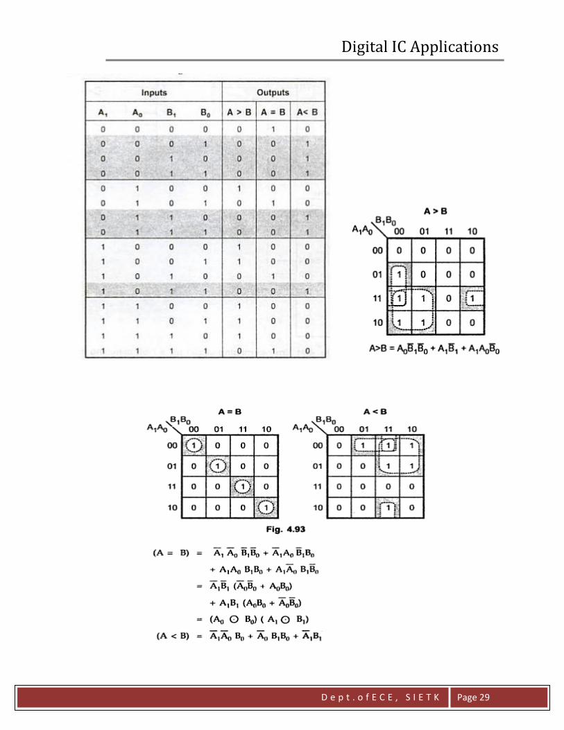
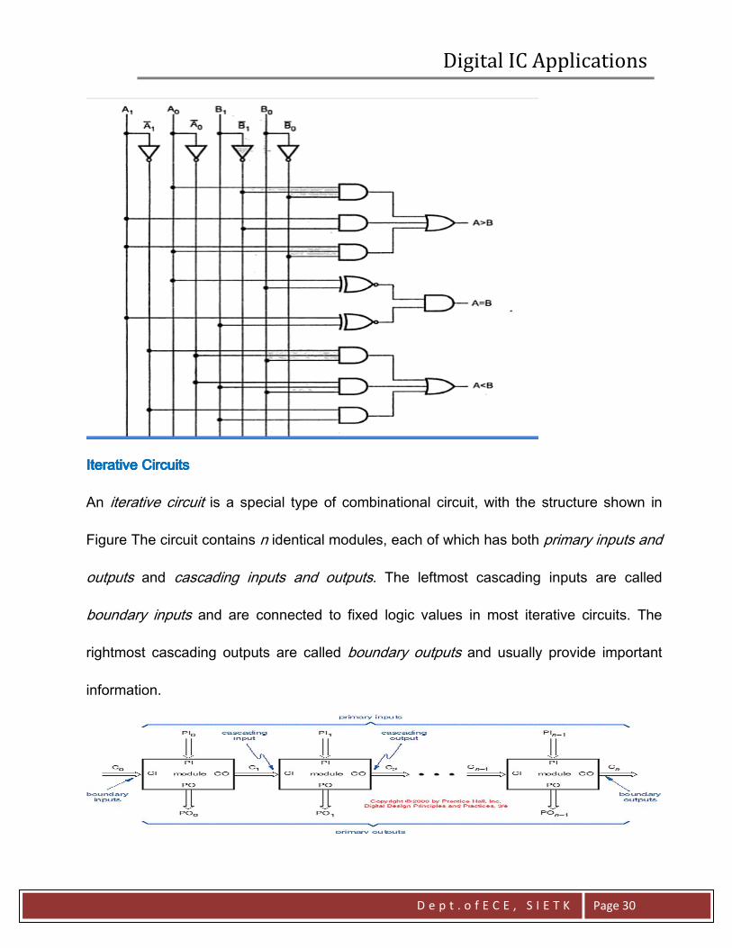
ComparatorsComparatorsComparatorsComparators
Comparing two binary words for equality is a commonly used operation in computer
systems and device interfaces. we showed a system structure in which devices are
enabled by comparing a “device select” word with a predetermined “device ID.” A circuit
that compares two binary words and indicates whether they are equal is called a
comparator. Some comparators interpret their input words as signed or unsigned numbers
and also indicate an arithmetic relationship (greater or less than) between the words.
These devices are often called magnitude comparators.
Digital IC Applications
D e p t . o f E C E , S I E T K
Page 29
Digital IC Applications
D e p t . o f E C E , S I E T K
Page 30
Iterative CircuitsIterative CircuitsIterative CircuitsIterative Circuits
An iterative circuit is a special type of combinational circuit, with the structure shown in
Figure The circuit contains n identical modules, each of which has both primary inputs and
outputs and cascading inputs and outputs. The leftmost cascading inputs are called
boundary inputs and are connected to fixed logic values in most iterative circuits. The
rightmost cascading outputs are called boundary outputs and usually provide important
information.

Digital IC Applications
D e p t . o f E C E , S I E T K
Page 31
Iterative circuits are well suited to problems that can be solved by a simple iterative
algorithm:
1. Set C0 to its initial value and set i to 0.
2. Use Ci and PIi to determine the values of POi and Ci+1.
3. Increment i.
4. If i < n, go to step 2.
AN ITERATIVE COMPARATORAN ITERATIVE COMPARATORAN ITERATIVE COMPARATORAN ITERATIVE COMPARATOR
The n-bit comparators in the preceding subsection might be called parallel comparators
because they look at each pair of input bits simultaneously and deliver the 1-bit
comparison results in parallel to an n-input OR or AND function. It is also possible to
design an “iterative comparator” that looks at its bits one at a time using a small, fixed
amount of logic per bit.
An Iterative Comparator CircuitAn Iterative Comparator CircuitAn Iterative Comparator CircuitAn Iterative Comparator Circuit
Two n-bit values X and Y can be compared one bit at a time using a single bit EQi at each
step to keep track of whether all of the bit-pairs have been equal so far:
1. Set EQ0 to 1 and set i to 0.
2. If EQi is 1 and Xi and Yi are equal, set EQi 1 to 1. Else set EQi1 to 0.
3. Increment i.
4. If i < n, go to step 2.

Digital IC Applications
D e p t . o f E C E , S I E T K
Page 32
Figure shows a corresponding iterative circuit. Note that this circuit has no primary
outputs; the boundary output is all that interests us. Other iterative circuits, such as the
ripple adder have primary outputs of interest. Given a choice between the iterative
comparator circuit in this subsection and one of the parallel comparators shown
previously, you would probably prefer the parallel comparator. The iterative comparator
saves little if any cost, and it’s very slow because the cascading signals need time to
“ripple” from the leftmost to the rightmost module. Iterative circuits that process more than
one bit
Standard MSI ComparatorsStandard MSI ComparatorsStandard MSI ComparatorsStandard MSI Comparators
Comparator applications are common enough that several MSI comparators have been
developed commercially. The 74x85 is a 4-bit comparator with the logic symbol shown in
Figure. It provides a greater-than output (AGTBOUT) and a less-than output (ALTBOUT)
as well as an equal output (AEQBOUT). The ’85 also has cascading inputs (AGTBIN,
ALTBIN, AEQBIN) for combining multiple ’85s to create comparators for more than four
bits. Both the cascading inputs and the outputs are arranged in a 1-out-of-3 code, since in
normal operation exactly one input and one output should be asserted. The cascading

Digital IC Applications
D e p t . o f E C E , S I E T K
Page 33
inputs are defined so the outputs of an ’85 that compares less-significant bits are
connected to the inputs of an ’85 that compares more.
4 bit comparator
3 outputs : A=B, A<B, A>B
3 Cascading inputs
Functional Output equations :
(A>B OUT)= (A>B)+(A=B).(A>B IN)
(A<B OUT)= (A<B)+(A=B).(A<B IN)
(A=B OUT)= (A=B).(A=B IN)
Cascading inputs initial values:
(A=B IN) =1
(A>B IN) =0
(A<B IN) =0
significant bits, as shown in Figure for a 12-bit comparator. This is an iterative circuit
according to the definition Each ’85 develops its cascading outputs roughly according to

Digital IC Applications
D e p t . o f E C E , S I E T K
Page 34
the following pseudo-logic equations: The parenthesized subexpressions above are not
normal logic expressions, but indicate an arithmetic comparison that occurs between the
A3–A0 and B3–B0 inputs. In other words, AGTBOUT is asserted if A > B or if A �B and
AGTBIN is asserted (if the higher-order bits are equal, we have to look at the lower-order
bits for the answer).

Digital IC Applications
D e p t . o f E C E , S I E T K
Page 35
Adders, Subtractors, and ALUsAdders, Subtractors, and ALUsAdders, Subtractors, and ALUsAdders, Subtractors, and ALUs
Addition is the most commonly performed arithmetic operation in digital systems. An adder
combines two arithmetic operands using the addition rules. the same addition rules and
therefore the same adders are used for both unsigned and two’s-complement numbers.
An adder can perform subtraction as the addition of the minuend and the complemented
(negated) subtrahend, but you can also build subtractor
Half Adder: adds two 1-bit operands
Half Adders and Full AddersHalf Adders and Full AddersHalf Adders and Full AddersHalf Adders and Full Adders
The simplest adder, called a half adder, adds two 1-bit operands X and Y, producing a 2-
bit sum. The sum can range from 0 to 2, which requires two bits to express. The low-order
bit of the sum may be named HS (half sum), and the high-order bit may be named CO
(carry out). We can write the following equations for HS and CO:
Digital IC Applications
D e p t . o f E C E , S I E T K
Page 36
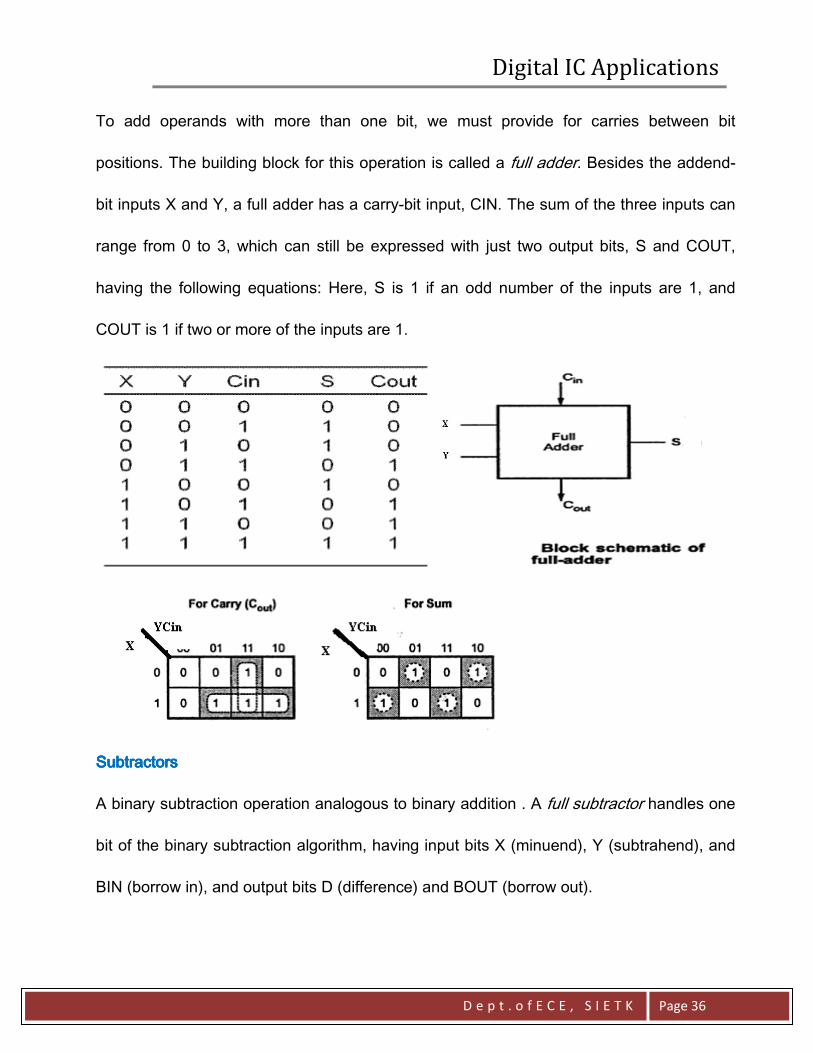
To add operands with more than one bit, we must provide for carries between bit
positions. The building block for this operation is called a full adder. Besides the addend-
bit inputs X and Y, a full adder has a carry-bit input, CIN. The sum of the three inputs can
range from 0 to 3, which can still be expressed with just two output bits, S and COUT,
having the following equations: Here, S is 1 if an odd number of the inputs are 1, and
COUT is 1 if two or more of the inputs are 1.
SubtractorsSubtractorsSubtractorsSubtractors
A binary subtraction operation analogous to binary addition . A full subtractor handles one
bit of the binary subtraction algorithm, having input bits X (minuend), Y (subtrahend), and
BIN (borrow in), and output bits D (difference) and BOUT (borrow out).

Digital IC Applications
D e p t . o f E C E , S I E T K
Page 37
X,Y are n-bit unsigned binary numbers
Addition : S = X + Y
Subtraction : D = X - Y = X + (-Y) =
= X+ (Two’s Complement of Y)
= X+ (One’s Complement of Y) + 1
= X+ Y’+ 1
Using Adder as a SubtractorUsing Adder as a SubtractorUsing Adder as a SubtractorUsing Adder as a Subtractor
MSI ADDERS
MSI ADDERSMSI ADDERS
MSI ADDERS
The 74x283 is a 4-bit binary adder that forms its sum and carry outputs with just a few
levels of logic, using the carry lookahead technique. The older 74x83 is identical except for
its pinout, which has nonstandard locations for power and ground. The logic diagram for
the ’283, has just a few differences from the general carry-lookahead design that we
described in the preceding subsection. First of all, its addends are named A and B instead
of X and Y; no big deal. Second, it produces active-low versions of the carry-generate (gi
�) and carrypropagate (pi �) signals, since inverting gates are generally faster than
noninverting ones. Third, it takes advantage of the fact that we can algebraically
manipulate the half-sum equation as follows: Thus, an AND gate with an inverted input

Digital IC Applications
D e p t . o f E C E , S I E T K
Page 38
can be used instead of an XOR gate to create each half-sum bit. Finally, the ’283 creates
the carry signals using an INVERT-OR-AND structure (the DeMorgan equivalent of an
AND-OR-INVERT), which has about the same delay as a single CMOS or TTL inverting
gate. This requires some explaining, since the carry equations that we derived in the
preceding subsection are used in a slightly modified form. In particular, the ci1 equation
uses the term pi �gi instead of gi. This has no effect on the output, since pi is always 1
when gi is 1. However, it allows the equation to be factored as follows: This leads to the
following carry equations, which are used by the circuit :
The propagation delay from the C0 input to the C4 output of the ’283 is very short, about
the same as two inverting gates. As a result, fairly fast groupripple adders with more than
four bits can be made simply by cascading the carry outputs and inputs of ’283s, as shown
in Figure for a 16-bit adder. The total propagation delay from C0 to C16 in this circuit is
about the same as that of eight inverting gates.

Digital IC Applications
D e p t . o f E C E , S I E T K
Page 39
MSI Arithmetic and Logic UnitsMSI Arithmetic and Logic UnitsMSI Arithmetic and Logic UnitsMSI Arithmetic and Logic Units
An arithmetic and logic unit (ALU) is a combinational circuit that can perform any of a
number of different arithmetic and logical operations on a pair of b-bit operands. The
operation to be performed is specified by a set of function-select inputs. Typical MSI ALUs
have 4-bit operands and three to five function select inputs, allowing up to 32 different
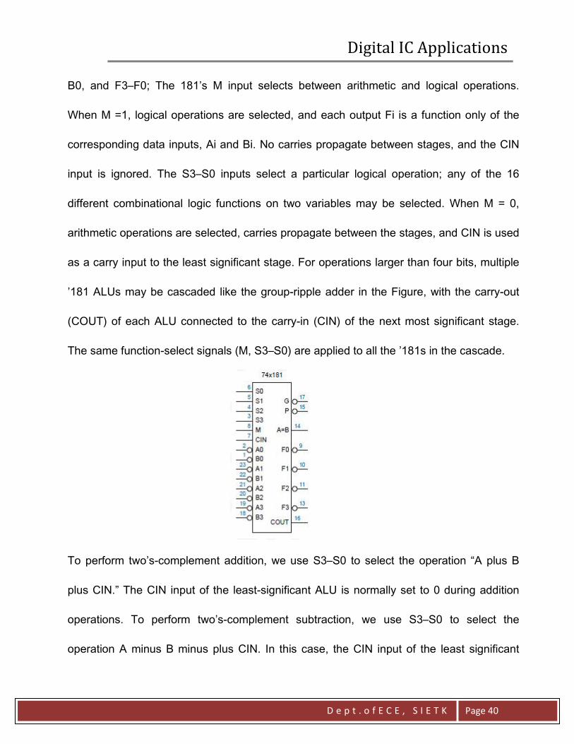
functions to be performed. Figure is a logic symbol for the 74x181 4-bit ALU. The
operation performed by the ’181 is selected by the M and S3–S0 inputs, as detailed in
Table. Note that the identifiers A, B, and F in the table refer to the 4-bit words A3–A0, B3–
Digital IC Applications
D e p t . o f E C E , S I E T K
Page 40
B0, and F3–F0; The 181’s M input selects between arithmetic and logical operations.
When M =1, logical operations are selected, and each output Fi is a function only of the
corresponding data inputs, Ai and Bi. No carries propagate between stages, and the CIN
input is ignored. The S3–S0 inputs select a particular logical operation; any of the 16
different combinational logic functions on two variables may be selected. When M = 0,
arithmetic operations are selected, carries propagate between the stages, and CIN is used
as a carry input to the least significant stage. For operations larger than four bits, multiple
’181 ALUs may be cascaded like the group-ripple adder in the Figure, with the carry-out
(COUT) of each ALU connected to the carry-in (CIN) of the next most significant stage.
The same function-select signals (M, S3–S0) are applied to all the ’181s in the cascade.
To perform two’s-complement addition, we use S3–S0 to select the operation “A plus B
plus CIN.” The CIN input of the least-significant ALU is normally set to 0 during addition
operations. To perform two’s-complement subtraction, we use S3–S0 to select the
operation A minus B minus plus CIN. In this case, the CIN input of the least significant

Digital IC Applications
D e p t . o f E C E , S I E T K
Page 41
ALU is normally set to 1, since CIN acts as the complement of the borrow during
subtraction. The ’181 provides other arithmetic operations, such as “A minus 1 plus CIN,”
that are useful in some applications (e.g., decrement by 1). It also provides a bunch of
weird arithmetic operations, such as “A �B�plus (A B) plus CIN,” that are
almost never used in practice, but that “fall out” of the circuit for free. Notice that the
operand inputs A3_L–A0_L and B3_L– B0_L and the function outputs F3_L–F0_L of the
’181 are active low. The ’181 can also be used with active-high operand inputs and
function outputs. In this case, a different version of the function table must be constructed.
When M �1, logical operations are still performed, but for a given input combination on
S3–S0, the function obtained is precisely the dual of the one listed in Table . When M
�0, arithmetic operations are performed, but the function table is once again different.

Digital IC Applications
D e p t . o f E C E , S I E T K
Page 42
Combinational MultipliersCombinational MultipliersCombinational MultipliersCombinational Multipliers
Combinational Multiplier StructuresCombinational Multiplier StructuresCombinational Multiplier StructuresCombinational Multiplier Structures
Multiplier has an algorithm that uses n shifts and adds to multiply n-bit binary numbers.
Although the shift-and-add algorithm emulates the way that we do paper-and-pencil
multiplication of decimal numbers, there is nothing inherently “sequential” or “time
dependent” about multiplication. That is, given two n-bit input words X and Y, it is possible
to write a truth table that expresses the 2n-bit product P �X�Y as a combinational
function of X and Y. A combinational multiplier is a logic circuit with such a truth table.
Most approaches to combinational multiplication are based on the paperand- pencil shift-
andadd algorithm. Figure 5-96 illustrates the basic idea for an 8x8 multiplier for two
unsigned integers, multiplicand X = x7x6x5x4x3x2x1x0 and multiplier Y =
y7y6y5y4y3y2y1y0. We call each row a product component, a shifted multiplicand that is
multiplied by 0 or 1 depending on the corresponding multiplier bit. Each small box
represents one product-component bit yixj, the logical AND of multiplier bit yi and
multiplicand bit xj. The product P = p15p14 . ..p2p1p0 has 16 bits and is obtained by
adding together all the product components. Figure shows one way to add up the product
components. Here, the product-component bits have been spread out to make space, and
each “+” box is a full adder equivalent to Figure 5- 85(c) on page 391. The carries in each
row of full adders are connected to make an 8-bit ripple adder. Thus, the first ripple adder

Digital IC Applications
D e p t . o f E C E , S I E T K
Page 43
combines the first two product components to product the first partial product. Subsequent
adders combine each partial product with the next product component.
Sequential multipliers use a single adder and a register to accumulate the partial
products. The partial-product register is initialized to the first product component, and for
an n�n-bit multiplication, n1 steps are taken and the adder is used n1 times, once for
each of the remaining n1 product components to be added to the partial-product
register. Some sequential multipliers use a trick called carry-save addition to speed up
multiplication. The idea is to break the carry chain of the ripple adder to shorten the delay
of each addition. This is done by applying the carry output from bit i during step j to the
carry input for bit i+1 during the next step, j+1. After the last product component is added,
one more step is needed in which the carries are hooked up in the usual way and allowed
to ripple from the least to the most significant bit.

Digital IC Applications
D e p t . o f E C E , S I E T K
Page 44
4X4 combinational multiplier with carry save
Digital IC Applications
D e p t . o f E C E , S I E T K
Page 45
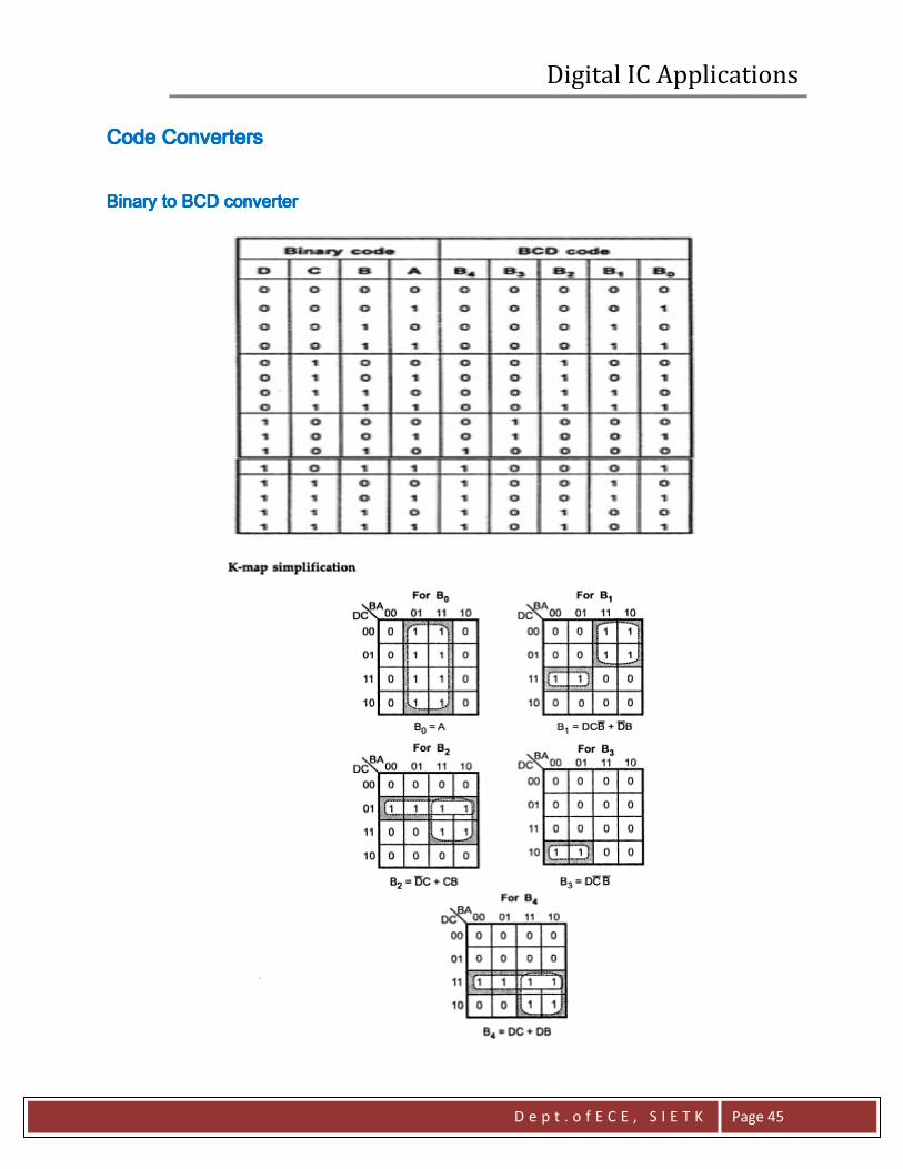
Code ConvertersCode ConvertersCode ConvertersCode Converters
Binary to BCD converterBinary to BCD converterBinary to BCD converterBinary to BCD converter

Digital IC Applications
D e p t . o f E C E , S I E T K
Page 46
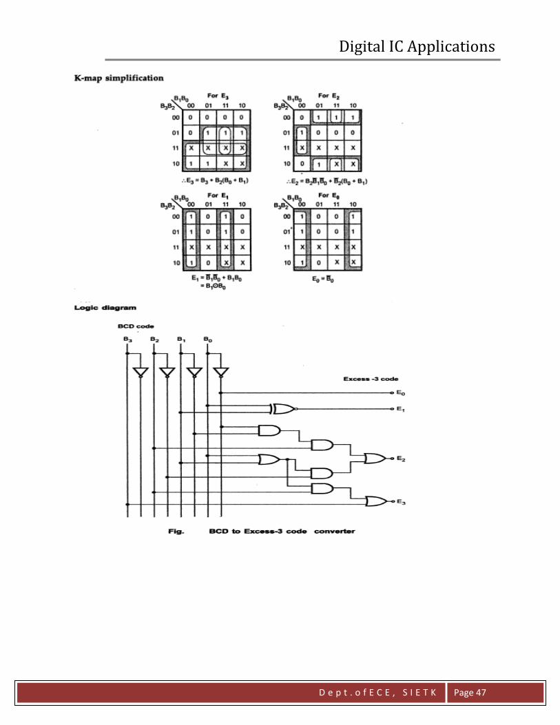
BCD to ExcessBCD to ExcessBCD to ExcessBCD to Excess----3 code converter3 code converter3 code converter3 code converter
Digital IC Applications
D e p t . o f E C E , S I E T K
Page 47

Digital IC Applications
D e p t . o f E C E , S I E T K
Page 48
Digital IC Applications
D e p t . o f E C E , S I E T K
Page 49
Digital IC Applications
D e p t . o f E C E , S I E T K
Page 50
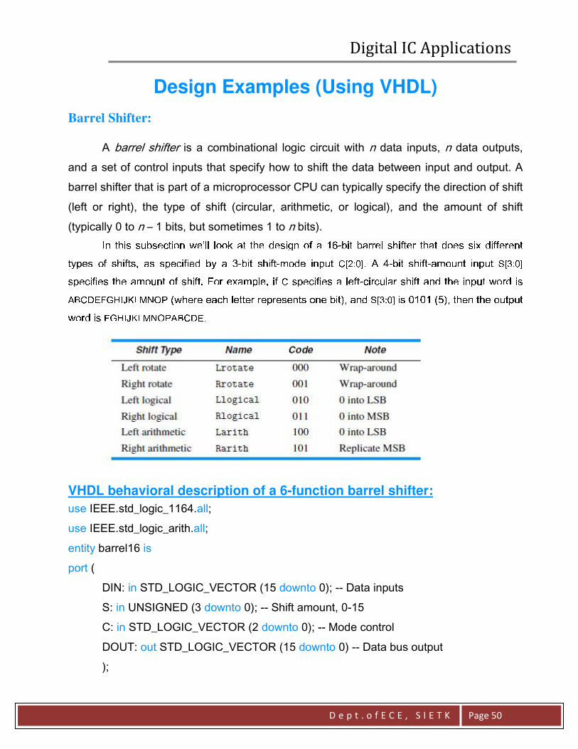
Design Examples (Using VHDL)
Barrel Shifter:
A barrel shifter is a combinational logic circuit with n data inputs, n data outputs,
and a set of control inputs that specify how to shift the data between input and output. A
barrel shifter that is part of a microprocessor CPU can typically specify the direction of shift
(left or right), the type of shift (circular, arithmetic, or logical), and the amount of shift
(typically 0 to n – 1 bits, but sometimes 1 to n bits).
In this subsection we’ll look at the design of a 16-bit barrel shifter that does six different
types of shifts, as specified by a 3-bit shift-mode input C[2:0]. A 4-bit shift-amount input S[3:0]
specifies the amount of shift. For example, if C specifies a left-circular shift and the input word is
ABCDEFGHIJKLMNOP (where each letter represents one bit), and S[3:0] is 0101 (5), then the output
word is FGHIJKLMNOPABCDE.
VHDL behavioral description of a 6-function barrel shifter:
use IEEE.std_logic_1164.all;
use IEEE.std_logic_arith.all;
entity barrel16 is
port (
DIN: in STD_LOGIC_VECTOR (15 downto 0); -- Data inputs
S: in UNSIGNED (3 downto 0); -- Shift amount, 0-15
C: in STD_LOGIC_VECTOR (2 downto 0); -- Mode control
DOUT: out STD_LOGIC_VECTOR (15 downto 0) -- Data bus output
);

Digital IC Applications
D e p t . o f E C E , S I E T K
Page 51
constant Lrotate: STD_LOGIC_VECTOR := "000"; -- Define the coding of
constant Rrotate: STD_LOGIC_VECTOR := "001"; -- the different shift modes
constant Llogical: STD_LOGIC_VECTOR := "010";
constant Rlogical: STD_LOGIC_VECTOR := "011";
constant Larith: STD_LOGIC_VECTOR := "100";
constant Rarith: STD_LOGIC_VECTOR := "101";
end barrel16;
architecture barrel16_behavioral of barrel16 is
subtype DATAWORD is STD_LOGIC_VECTOR(15 downto 0);
function Vrol (D: DATAWORD; S: UNSIGNED)
return DATAWORD is
variable N: INTEGER;
variable TMPD: DATAWORD;
begin
N := CONV_INTEGER(S); TMPD := D;
for i in 1 to N loop
TMPD := TMPD(14 downto 0) & TMPD(15);
end loop;
return TMPD;
end Vrol;
...
begin
process(DIN, S, C)
begin
case C is
when Lrotate => DOUT <= Vrol(DIN,S);
when Rrotate => DOUT <= Vror(DIN,S);
when Illogical => DOUT <= Vsll(DIN,S);
when Rlogical => DOUT <= Vsrl(DIN,S);
when Larith => DOUT <= Vsla(DIN,S);

Digital IC Applications
D e p t . o f E C E , S I E T K
Page 52
when Rarith => DOUT <= Vsra(DIN,S);
when others => DOUT <= DIN;
end case;
end process;
end barrel16_behavioral;
VHDL program for a 16VHDL program for a 16VHDL program for a 16VHDL program for a 16----bit barrel shifter for left circbit barrel shifter for left circbit barrel shifter for left circbit barrel shifter for left circular shifts onlyular shifts onlyular shifts onlyular shifts only:
library IEEE;
use IEEE.std_logic_1164.all;
entity rol16 is
port (
DIN: in STD_LOGIC_VECTOR(15 downto 0); -- Data inputs
S: in STD_LOGIC_VECTOR (3 downto 0); -- Shift amount, 0-15
DOUT: out STD_LOGIC_VECTOR(15 downto 0) -- Data bus output
);
end rol16;
architecture rol16_arch of rol16 is
begin
process(DIN, S)
variable X, Y, Z: STD_LOGIC_VECTOR(15 downto 0);
begin
if S(0)='1' then X := DIN(14 downto 0) & DIN(15); else X := DIN; end if;
if S(1)='1' then Y := X(13 downto 0) & X(15 downto 14); else Y := X; end if;
if S(2)='1' then Z := Y(11 downto 0) & Y(15 downto 12); else Z := Y; end if;
if S(3)='1' then DOUT <= Z(7 downto 0) & Z(15 downto 8); else DOUT <= Z; end if;
end process;
end rol16_arch;

Digital IC Applications
D e p t . o f E C E , S I E T K
Page 53
Comparator:Comparator:Comparator:Comparator:
VHDL program for an VHDL program for an VHDL program for an VHDL program for an 8888----bit comparatbit comparatbit comparatbit comparator:or:or:or:
library IEEE;
use IEEE.std_logic_1164.all;
use IEEE.std_logic_unsigned.all;
entity comp8 is
port ( A, B: in STD_LOGIC_VECTOR (7 downto 0);
EQ, GT: out STD_LOGIC );
end comp8;
architecture comp8_arch of comp8 is
begin
EQ <= '1' when A = B else '0';
GT <= '1' when A > B else '0';
end comp8_arch;
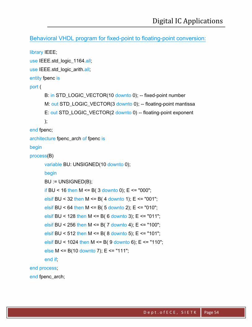
FloatingFloatingFloatingFloating----point Encoder:point Encoder:point Encoder:point Encoder:
An unsigned binary integer B in the range 0 ≤ B < 211 can be represented by 11 bits in
“fixed-point” format, B = b10b9…b1b0. We can represent numbers in the same range with
less precision using only 7 bits in a floating-point notation, F = M⋅ 2E, where M is a 4-bit
mantissa m3m2m1m0 and E is a 3-bit exponent e2e1e0. The smallest integer in this
format is 0⋅20 and the largest is (24−1) ⋅ 27. Given an 11-bit fixed-point integer B, we can
convert it to our 7-bit floating-point notation by “picking off” four high-order bits beginning
with the most significant 1, for example, The last term in each equation is a truncation
error that results from the loss of precision in the conversion. Corresponding to this
conversion operation, we can write the specification for a fixed-point to floating-point
encoder circuit:
• A combinational circuit is to convert an 11-bit unsigned binary integer B into a 7-bit
floating-point number M,E, where M and E have 4 and 3 bits, respectively. The numbers
have the relationship B = M⋅2E + T, where T is the truncation error, 0 ≤ T< 2E.
Digital IC Applications
D e p t . o f E C E , S I E T K
Page 54
Behavioral VHDL program for fixed-point to floating-point conversion:
library IEEE;
use IEEE.std_logic_1164.all;
use IEEE.std_logic_arith.all;
entity fpenc is
port (
B: in STD_LOGIC_VECTOR(10 downto 0); -- fixed-point number
M: out STD_LOGIC_VECTOR(3 downto 0); -- floating-point mantissa
E: out STD_LOGIC_VECTOR(2 downto 0) -- floating-point exponent
);
end fpenc;
architecture fpenc_arch of fpenc is
begin
process(B)
variable BU: UNSIGNED(10 downto 0);
begin
BU := UNSIGNED(B);
if BU < 16 then M <= B( 3 downto 0); E <= "000";
elsif BU < 32 then M <= B( 4 downto 1); E <= "001";
elsif BU < 64 then M <= B( 5 downto 2); E <= "010";
elsif BU < 128 then M <= B( 6 downto 3); E <= "011";
elsif BU < 256 then M <= B( 7 downto 4); E <= "100";
elsif BU < 512 then M <= B( 8 downto 5); E <= "101";
elsif BU < 1024 then M <= B( 9 downto 6); E <= "110";
else M <= B(10 downto 7); E <= "111";
end if;
end process;
end fpenc_arch;

Digital IC Applications
D e p t . o f E C E , S I E T K
Page 55
Alternative VHDL architecture for fixed-point to floating-point conversion:
architecture fpence_arch of fpenc is
begin
process(B)
begin
if B(10) = '1' then M <= B(10 downto 7); E <= "111";
elsif B(9) = '1' then M <= B( 9 downto 6); E <= "110";
elsif B(8) = '1' then M <= B( 8 downto 5); E <= "101";
elsif B(7) = '1' then M <= B( 7 downto 4); E <= "100";
elsif B(6) = '1' then M <= B( 6 downto 3); E <= "011";
elsif B(5) = '1' then M <= B( 5 downto 2); E <= "010";
elsif B(4) = '1' then M <= B( 4 downto 1); E <= "001";
else M <= B( 3 downto 0); E <= "000";
end if;
end process;
end fpence_arch;
Behavioral VHDL architecture for fixed-point to floating-point conversion with
rounding:
architecture fpencr_arch of fpenc is
function round (BSLICE: STD_LOGIC_VECTOR(4 downto 0))
return STD_LOGIC_VECTOR is
variable BSU: UNSIGNED(3 downto 0);
begin
if BSLICE(0) = '0' then return BSLICE(4 downto 1);
else
BSU := UNSIGNED(BSLICE(4 downto 1)) + 1;
return STD_LOGIC_VECTOR(BSU);
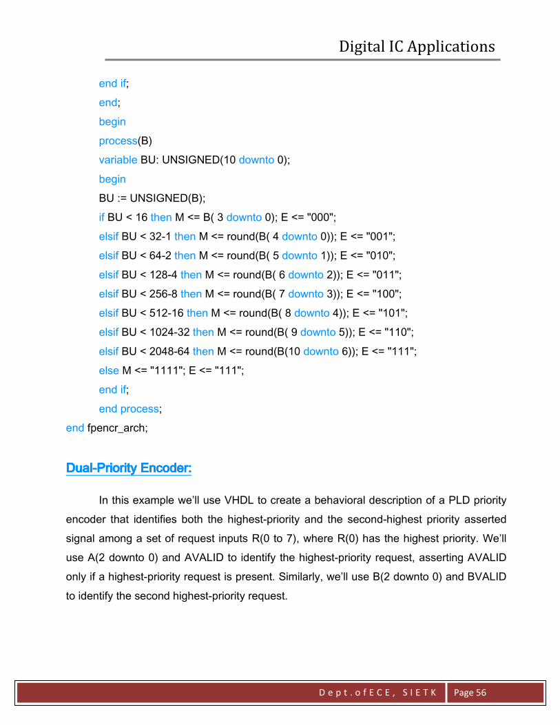
Digital IC Applications
D e p t . o f E C E , S I E T K
Page 56
end if;
end;
begin
process(B)
variable BU: UNSIGNED(10 downto 0);
begin
BU := UNSIGNED(B);
if BU < 16 then M <= B( 3 downto 0); E <= "000";
elsif BU < 32-1 then M <= round(B( 4 downto 0)); E <= "001";
elsif BU < 64-2 then M <= round(B( 5 downto 1)); E <= "010";
elsif BU < 128-4 then M <= round(B( 6 downto 2)); E <= "011";
elsif BU < 256-8 then M <= round(B( 7 downto 3)); E <= "100";
elsif BU < 512-16 then M <= round(B( 8 downto 4)); E <= "101";
elsif BU < 1024-32 then M <= round(B( 9 downto 5)); E <= "110";
elsif BU < 2048-64 then M <= round(B(10 downto 6)); E <= "111";
else M <= "1111"; E <= "111";
end if;
end process;
end fpencr_arch;
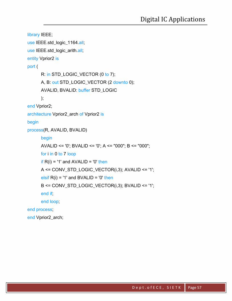
DualDualDualDual----Priority EncoderPriority EncoderPriority EncoderPriority Encoder::::
In this example we’ll use VHDL to create a behavioral description of a PLD priority
encoder that identifies both the highest-priority and the second-highest priority asserted
signal among a set of request inputs R(0 to 7), where R(0) has the highest priority. We’ll
use A(2 downto 0) and AVALID to identify the highest-priority request, asserting AVALID
only if a highest-priority request is present. Similarly, we’ll use B(2 downto 0) and BVALID
to identify the second highest-priority request.
Digital IC Applications
D e p t . o f E C E , S I E T K
Page 57
library IEEE;
use IEEE.std_logic_1164.all;
use IEEE.std_logic_arith.all;
entity Vprior2 is
port (
R: in STD_LOGIC_VECTOR (0 to 7);
A, B: out STD_LOGIC_VECTOR (2 downto 0);
AVALID, BVALID: buffer STD_LOGIC
);
end Vprior2;
architecture Vprior2_arch of Vprior2 is
begin
process(R, AVALID, BVALID)
begin
AVALID <= '0'; BVALID <= '0'; A <= "000"; B <= "000";
for i in 0 to 7 loop
if R(i) = '1' and AVALID = '0' then
A <= CONV_STD_LOGIC_VECTOR(i,3); AVALID <= '1';
elsif R(i) = '1' and BVALID = '0' then
B <= CONV_STD_LOGIC_VECTOR(i,3); BVALID <= '1';
end if;
end loop;
end process;
end Vprior2_arch;
Digital IC Applications
D e p t . o f E C E , S I E T K
Page 58
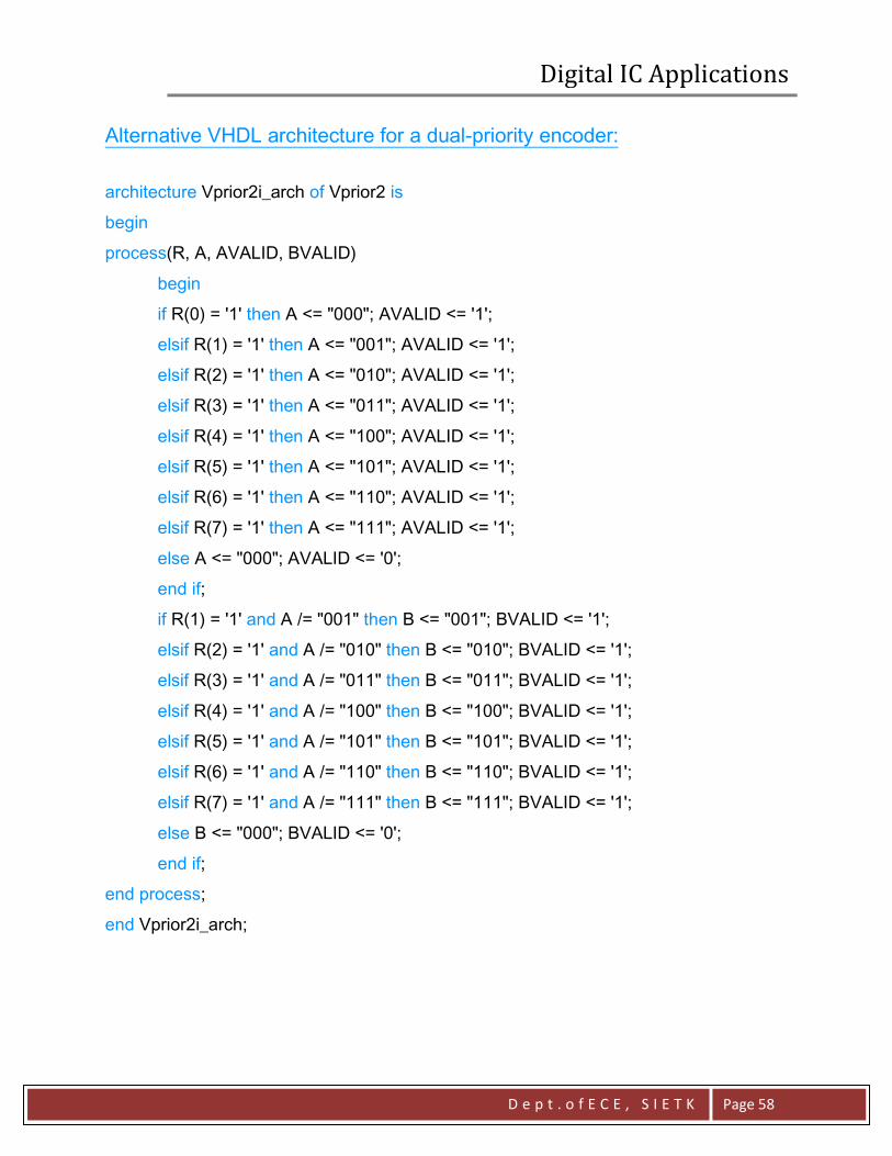
Alternative VHDL architecture for a dual-priority encoder:
architecture Vprior2i_arch of Vprior2 is
begin
process(R, A, AVALID, BVALID)
begin
if R(0) = '1' then A <= "000"; AVALID <= '1';
elsif R(1) = '1' then A <= "001"; AVALID <= '1';
elsif R(2) = '1' then A <= "010"; AVALID <= '1';
elsif R(3) = '1' then A <= "011"; AVALID <= '1';
elsif R(4) = '1' then A <= "100"; AVALID <= '1';
elsif R(5) = '1' then A <= "101"; AVALID <= '1';
elsif R(6) = '1' then A <= "110"; AVALID <= '1';
elsif R(7) = '1' then A <= "111"; AVALID <= '1';
else A <= "000"; AVALID <= '0';
end if;
if R(1) = '1' and A /= "001" then B <= "001"; BVALID <= '1';
elsif R(2) = '1' and A /= "010" then B <= "010"; BVALID <= '1';
elsif R(3) = '1' and A /= "011" then B <= "011"; BVALID <= '1';
elsif R(4) = '1' and A /= "100" then B <= "100"; BVALID <= '1';
elsif R(5) = '1' and A /= "101" then B <= "101"; BVALID <= '1';
elsif R(6) = '1' and A /= "110" then B <= "110"; BVALID <= '1';
elsif R(7) = '1' and A /= "111" then B <= "111"; BVALID <= '1';
else B <= "000"; BVALID <= '0';
end if;
end process;
end Vprior2i_arch;