Unit – 1 Session - 4 Digital Logic - BookSpar 33 LOGIC DESIGN UNIT – 1 Digital Principles,...
14
10CS 33 LOGIC DESIGN UNIT – 1 Digital Principles, Digital Logic B. S. Umashankar, BNMIT Page 1 Unit – 1 Session - 4 Digital Logic Objectives • Understand what are logic gates • Review Boolean Algebra • Write the truth tables for, and draw the symbols for, 2-input OR, AND, NOR, and NAND gates • Write Boolean equations for logic circuits and draw logic circuits for Boolean equations • Use De Morgan’s first and second theorems to create equivalent circuits • Positive and Negative Logic Introduction A digital electronic circuit having one or more input signals, but only one output signal is called a gate. Gates simulate mental processes; hence they are called logic gates. A logic gate performs a logical operation on one or more logic inputs and produces a single logic output. Review of Boolean Algebra Boolean algebra was developed in 1854 by George Boole. In 1937 Claude Shannon showed that Boolean algebra can be used to describe logic circuits. Boolean algebra is widely used in the design of digital circuits and computers. It is the mathematical foundation of logic design. Boolean Algebra Definition A Boolean algebra is an algebra consisting of a set B (which contains at least two elements 0 and 1) together with three operations : AND, OR, NOT defined on the set, such that for any element x and y of B, x . y (the product of x and y), x + y (the sum of x and y ) and x’ (the complement of x ) are in B. Axioms of Boolean Algebra 0 . 0 = 0 1 + 1 = 1 1 . 1 = 1 0 + 0 = 0 0 . 1 = 0 1 + 0 = 1 1 . 0 = 0 0 + 1 = 1 If x = 0, then x’ = 1 and If x = 1, then x’ = 0. www.bookspar.com | VTU NOTES | QUESTION PAPERS | NEWS | RESULTS | FORUMS
-
Upload
hoangquynh -
Category
Documents
-
view
241 -
download
2
Transcript of Unit – 1 Session - 4 Digital Logic - BookSpar 33 LOGIC DESIGN UNIT – 1 Digital Principles,...
10CS 33 LOGIC DESIGN UNIT – 1 Digital Principles, Digital Logic
B. S. Umashankar, BNMIT Page 1
Unit – 1
Session - 4
Digital Logic
Objectives
• Understand what are logic gates
• Review Boolean Algebra
• Write the truth tables for, and draw the symbols for, 2-input OR, AND, NOR, and NAND gates
• Write Boolean equations for logic circuits and draw logic circuits for Boolean equations
• Use De Morgan’s first and second theorems to create equivalent circuits
• Positive and Negative Logic
Introduction
A digital electronic circuit having one or more input signals, but only one output signal is called a gate.
Gates simulate mental processes; hence they are called logic gates. A logic gate performs a logical
operation on one or more logic inputs and produces a single logic output.
Review of Boolean Algebra
Boolean algebra was developed in 1854 by George Boole. In 1937 Claude Shannon showed that Boolean
algebra can be used to describe logic circuits. Boolean algebra is widely used in the design of digital
circuits and computers. It is the mathematical foundation of logic design.
Boolean Algebra Definition
A Boolean algebra is an algebra consisting of a set B (which contains at least two elements 0 and 1)
together with three operations : AND, OR, NOT defined on the set, such that for any element x and y of
B, x . y (the product of x and y), x + y (the sum of x and y ) and x’ (the complement of x ) are in B.
Axioms of Boolean Algebra
0 . 0 = 0 1 + 1 = 1
1 . 1 = 1 0 + 0 = 0
0 . 1 = 0 1 + 0 = 1
1 . 0 = 0 0 + 1 = 1
If x = 0, then x’ = 1 and If x = 1, then x’ = 0.
www.bookspar.com | VTU NOTES | QUESTION PAPERS | NEWS | RESULTS | FORUMS
10CS 33 LOGIC DESIGN UNIT – 1 Digital Principles, Digital Logic
B. S. Umashankar, BNMIT Page 2
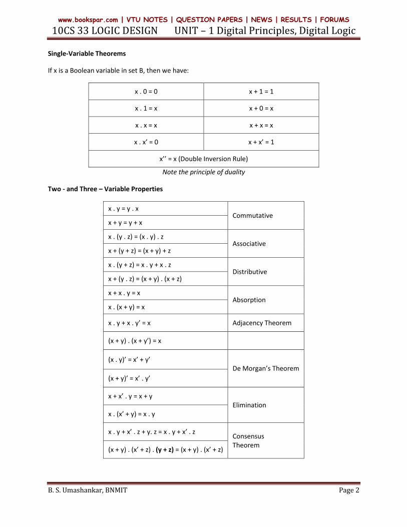
Single-Variable Theorems
If x is a Boolean variable in set B, then we have:
x . 0 = 0 x + 1 = 1
x . 1 = x x + 0 = x
x . x = x x + x = x
x . x’ = 0 x + x’ = 1
x’’ = x (Double Inversion Rule)
Note the principle of duality
Two - and Three – Variable Properties
x . y = y . x Commutative
x + y = y + x
x . (y . z) = (x . y) . z Associative
x + (y + z) = (x + y) + z
x . (y + z) = x . y + x . z Distributive
x + (y . z) = (x + y) . (x + z)
x + x . y = x Absorption
x . (x + y) = x
x . y + x . y’ = x Adjacency Theorem
(x + y) . (x + y’) = x
(x . y)’ = x’ + y’
De Morgan’s Theorem
(x + y)’ = x’ . y’
x + x’ . y = x + y
Elimination
x . (x’ + y) = x . y
x . y + x’ . z + y. z = x . y + x’ . z Consensus
Theorem (x + y) . (x’ + z) . (y + z) = (x + y) . (x’ + z)
www.bookspar.com | VTU NOTES | QUESTION PAPERS | NEWS | RESULTS | FORUMS
10CS 33 LOGIC DESIGN UNIT
B. S. Umashankar, BNMIT
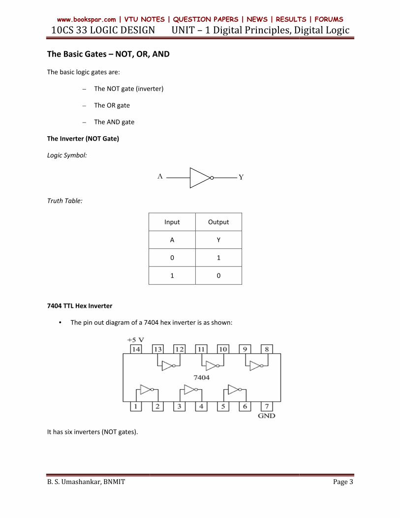
The Basic Gates – NOT, OR,
The basic logic gates are:
– The NOT gate (inverter)
– The OR gate
– The AND gate
The Inverter (NOT Gate)
Logic Symbol:
Truth Table:
7404 TTL Hex Inverter
• The pin out diagram of a 7404 hex inverter is as shown:
It has six inverters (NOT gates).
10CS 33 LOGIC DESIGN UNIT – 1 Digital Principles, Digital Logic
NOT, OR, AND
The NOT gate (inverter)
Input Output
A Y
0 1
1 0
diagram of a 7404 hex inverter is as shown:
1 Digital Principles, Digital Logic
Page 3
www.bookspar.com | VTU NOTES | QUESTION PAPERS | NEWS | RESULTS | FORUMS
10CS 33 LOGIC DESIGN UNIT
B. S. Umashankar, BNMIT
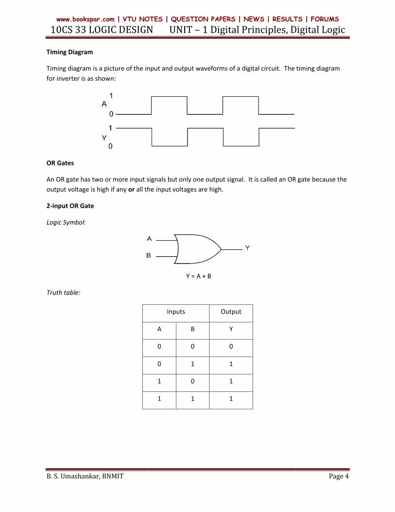
Timing Diagram
Timing diagram is a picture of the input and output waveforms of a digital circuit
for inverter is as shown:
OR Gates
An OR gate has two or more input signals but only one output signal
output voltage is high if any or all the input voltages are high
2-input OR Gate
Logic Symbol:
Truth table:
10CS 33 LOGIC DESIGN UNIT – 1 Digital Principles, Digital Logic
Timing diagram is a picture of the input and output waveforms of a digital circuit. The timing diagram
An OR gate has two or more input signals but only one output signal. It is called an OR gate because the
all the input voltages are high.
Y = A + B
Inputs Output
A B Y
0 0 0
0 1 1
1 0 1
1 1 1
1 Digital Principles, Digital Logic
Page 4
The timing diagram
called an OR gate because the
www.bookspar.com | VTU NOTES | QUESTION PAPERS | NEWS | RESULTS | FORUMS
10CS 33 LOGIC DESIGN UNIT
B. S. Umashankar, BNMIT
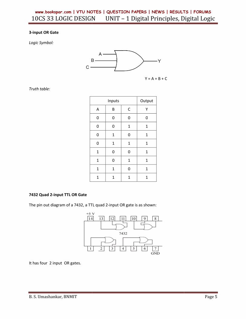
3-input OR Gate
Logic Symbol:
Truth table:
7432 Quad 2-input TTL OR Gate
The pin out diagram of a 7432, a TTL quad 2
It has four 2 input OR gates.
10CS 33 LOGIC DESIGN UNIT – 1 Digital Principles, Digital Logic
Y = A + B + C
Inputs Output
A B C Y
0 0 0 0
0 0 1 1
0 1 0 1
0 1 1 1
1 0 0 1
1 0 1 1
1 1 0 1
1 1 1 1
diagram of a 7432, a TTL quad 2-input OR gate is as shown:
1 Digital Principles, Digital Logic
Page 5
www.bookspar.com | VTU NOTES | QUESTION PAPERS | NEWS | RESULTS | FORUMS
10CS 33 LOGIC DESIGN UNIT
B. S. Umashankar, BNMIT
Timing Diagram of 2-input OR Gate
The timing diagram for a 2-input OR gate, when the two inputs given are as shown:
AND Gates
The AND gate has a high output only when all inputs are high
Logic Symbol:
Truth table of 2-input AND gate:
3-input AND Gate
Logic Symbol:
10CS 33 LOGIC DESIGN UNIT – 1 Digital Principles, Digital Logic
input OR Gate
input OR gate, when the two inputs given are as shown:
The AND gate has a high output only when all inputs are high.
Y = A . B
Inputs Output
A B Y
0 0 0
0 1 0
1 0 0
1 1 1
Y = A . B . C
1 Digital Principles, Digital Logic
Page 6
www.bookspar.com | VTU NOTES | QUESTION PAPERS | NEWS | RESULTS | FORUMS
10CS 33 LOGIC DESIGN UNIT
B. S. Umashankar, BNMIT
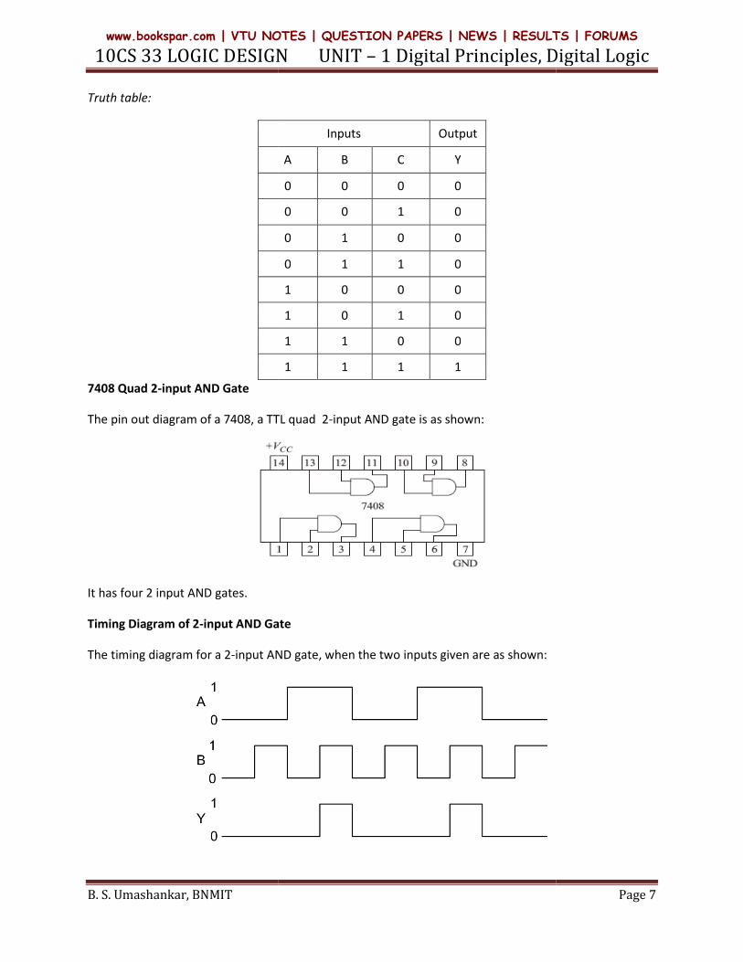
Truth table:
7408 Quad 2-input AND Gate
The pin out diagram of a 7408, a TTL quad
It has four 2 input AND gates.
Timing Diagram of 2-input AND Gate
The timing diagram for a 2-input AND gate, when the two inputs given are as shown:
10CS 33 LOGIC DESIGN UNIT – 1 Digital Principles, Digital Logic
Inputs Output
A B C Y
0 0 0 0
0 0 1 0
0 1 0 0
0 1 1 0
1 0 0 0
1 0 1 0
1 1 0 0
1 1 1 1
diagram of a 7408, a TTL quad 2-input AND gate is as shown:
input AND Gate
input AND gate, when the two inputs given are as shown:
1 Digital Principles, Digital Logic
Page 7
www.bookspar.com | VTU NOTES | QUESTION PAPERS | NEWS | RESULTS | FORUMS
10CS 33 LOGIC DESIGN UNIT
B. S. Umashankar, BNMIT
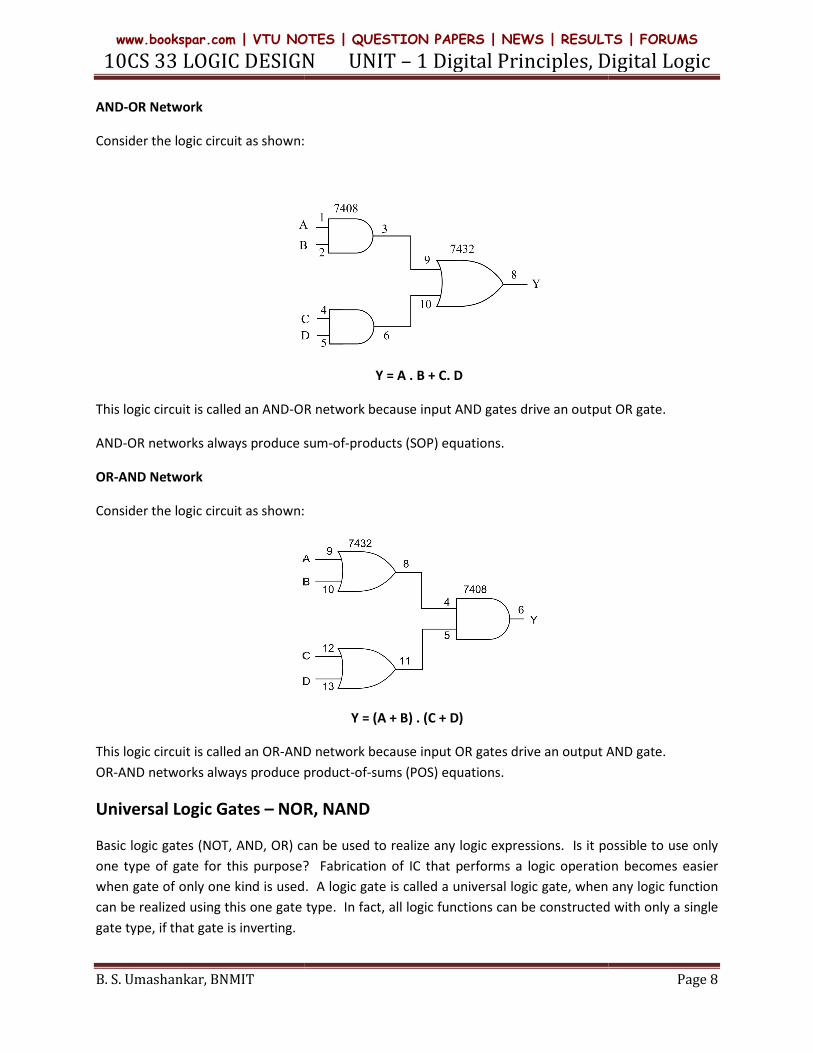
AND-OR Network
Consider the logic circuit as shown:
This logic circuit is called an AND-OR network because input AND gates drive an output OR gate.
AND-OR networks always produce sum
OR-AND Network
Consider the logic circuit as shown:
This logic circuit is called an OR-AND network because input OR gates drive an output AND gate.
OR-AND networks always produce product
Universal Logic Gates – NOR, NAND
Basic logic gates (NOT, AND, OR) can be us
one type of gate for this purpose?
when gate of only one kind is used
can be realized using this one gate type
gate type, if that gate is inverting.
10CS 33 LOGIC DESIGN UNIT – 1 Digital Principles, Digital Logic
as shown:
Y = A . B + C. D
OR network because input AND gates drive an output OR gate.
sum-of-products (SOP) equations.
Consider the logic circuit as shown:
Y = (A + B) . (C + D)
AND network because input OR gates drive an output AND gate.
AND networks always produce product-of-sums (POS) equations.
NOR, NAND
Basic logic gates (NOT, AND, OR) can be used to realize any logic expressions. Is it possible to use only
of gate for this purpose? Fabrication of IC that performs a logic operatio
gate of only one kind is used. A logic gate is called a universal logic gate, when any logic function
can be realized using this one gate type. In fact, all logic functions can be constructed with only a single
1 Digital Principles, Digital Logic
Page 8
OR network because input AND gates drive an output OR gate.
AND network because input OR gates drive an output AND gate.
Is it possible to use only
Fabrication of IC that performs a logic operation becomes easier
universal logic gate, when any logic function
In fact, all logic functions can be constructed with only a single
www.bookspar.com | VTU NOTES | QUESTION PAPERS | NEWS | RESULTS | FORUMS
10CS 33 LOGIC DESIGN UNIT
B. S. Umashankar, BNMIT
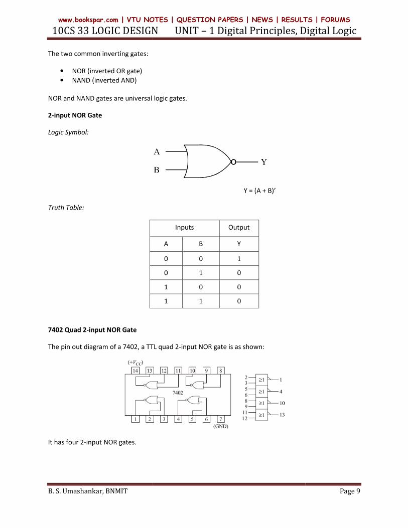
The two common inverting gates:
• NOR (inverted OR gate)
• NAND (inverted AND)
NOR and NAND gates are universal logic gates
2-input NOR Gate
Logic Symbol:
Truth Table:
7402 Quad 2-input NOR Gate
The pin out diagram of a 7402, a TTL quad
It has four 2-input NOR gates.
10CS 33 LOGIC DESIGN UNIT – 1 Digital Principles, Digital Logic
NOR and NAND gates are universal logic gates.
Y = (A + B)’
Inputs Output
A B Y
0 0 1
0 1 0
1 0 0
1 1 0
out diagram of a 7402, a TTL quad 2-input NOR gate is as shown:
1 Digital Principles, Digital Logic
Page 9
www.bookspar.com | VTU NOTES | QUESTION PAPERS | NEWS | RESULTS | FORUMS
10CS 33 LOGIC DESIGN UNIT
B. S. Umashankar, BNMIT
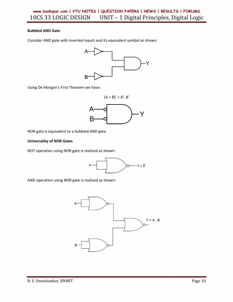
Bubbled AND Gate
Consider AND gate with inverted inputs and its equivalent symbol as shown:
Using De Morgan’s First Theorem we have:
NOR gate is equivalent to a bubbled
Universality of NOR Gates
NOT operation using NOR gate is realized as shown:
AND operation using NOR gate is realized as shown:
10CS 33 LOGIC DESIGN UNIT – 1 Digital Principles, Digital Logic
Consider AND gate with inverted inputs and its equivalent symbol as shown:
Using De Morgan’s First Theorem we have:
(A + B)’ = A’. B’
NOR gate is equivalent to a bubbled AND gate.
NOT operation using NOR gate is realized as shown:
AND operation using NOR gate is realized as shown:
1 Digital Principles, Digital Logic
Page 10
www.bookspar.com | VTU NOTES | QUESTION PAPERS | NEWS | RESULTS | FORUMS
10CS 33 LOGIC DESIGN UNIT
B. S. Umashankar, BNMIT
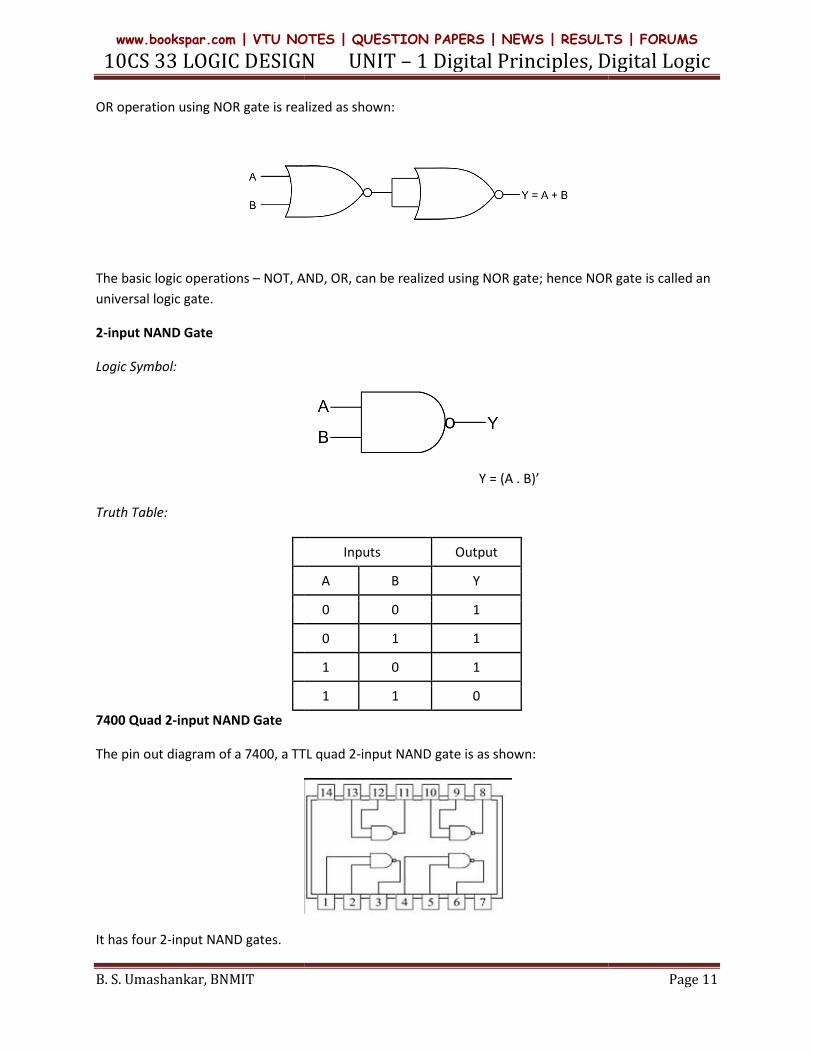
OR operation using NOR gate is realized as shown:
The basic logic operations – NOT, AND, OR, can be realize
universal logic gate.
2-input NAND Gate
Logic Symbol:
Truth Table:
7400 Quad 2-input NAND Gate
The pin out diagram of a 7400, a TTL quad 2
It has four 2-input NAND gates.
10CS 33 LOGIC DESIGN UNIT – 1 Digital Principles, Digital Logic
OR operation using NOR gate is realized as shown:
NOT, AND, OR, can be realized using NOR gate; hence NOR gate is called an
Y = (A . B)’
Inputs Output
A B Y
0 0 1
0 1 1
1 0 1
1 1 0
out diagram of a 7400, a TTL quad 2-input NAND gate is as shown:
1 Digital Principles, Digital Logic
Page 11
d using NOR gate; hence NOR gate is called an
www.bookspar.com | VTU NOTES | QUESTION PAPERS | NEWS | RESULTS | FORUMS
10CS 33 LOGIC DESIGN UNIT
B. S. Umashankar, BNMIT
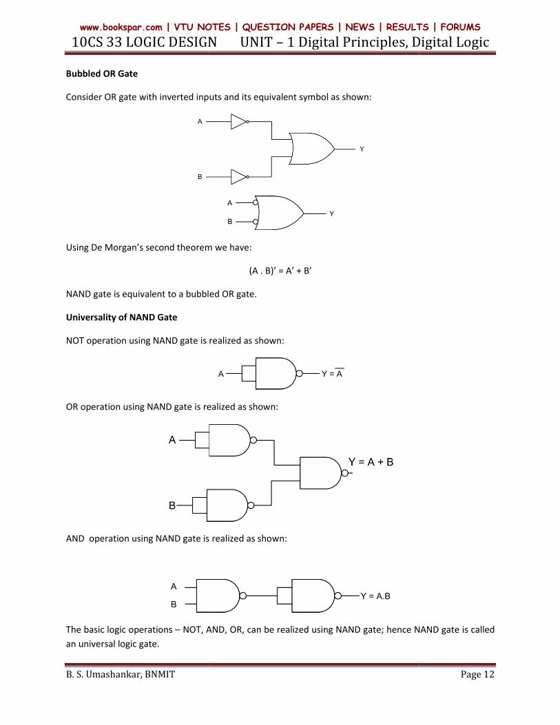
Bubbled OR Gate
Consider OR gate with inverted inputs and its equivalent symbol as shown:
Using De Morgan’s second theorem we have:
NAND gate is equivalent to a bubbled OR
Universality of NAND Gate
NOT operation using NAND gate is realized as shown:
OR operation using NAND gate is realized as shown:
AND operation using NAND gate is realized as shown:
The basic logic operations – NOT, AND, OR, can be realized
an universal logic gate.
10CS 33 LOGIC DESIGN UNIT – 1 Digital Principles, Digital Logic
Consider OR gate with inverted inputs and its equivalent symbol as shown:
heorem we have:
(A . B)’ = A’ + B’
NAND gate is equivalent to a bubbled OR gate.
NOT operation using NAND gate is realized as shown:
OR operation using NAND gate is realized as shown:
AND operation using NAND gate is realized as shown:
NOT, AND, OR, can be realized using NAND gate; hence NAND gate is called
1 Digital Principles, Digital Logic
Page 12
using NAND gate; hence NAND gate is called
www.bookspar.com | VTU NOTES | QUESTION PAPERS | NEWS | RESULTS | FORUMS
10CS 33 LOGIC DESIGN UNIT – 1 Digital Principles, Digital Logic
B. S. Umashankar, BNMIT Page 13
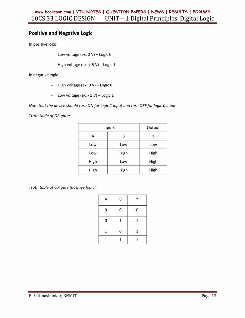
Positive and Negative Logic
In positive logic
– Low voltage (ex. 0 V) – Logic 0
– High voltage (ex. + 5 V) – Logic 1
In negative logic
– High voltage (ex. 0 V) – Logic 0
– Low voltage (ex. - 5 V) – Logic 1
Note that the device should turn ON for logic 1 input and turn OFF for logic 0 input.
Truth table of OR gate:
Inputs Output
A B Y
Low Low Low
Low High High
High Low High
High High High
Truth table of OR gate (positive logic):
A B Y
0 0 0
0 1 1
1 0 1
1 1 1
www.bookspar.com | VTU NOTES | QUESTION PAPERS | NEWS | RESULTS | FORUMS
10CS 33 LOGIC DESIGN UNIT – 1 Digital Principles, Digital Logic
B. S. Umashankar, BNMIT Page 14
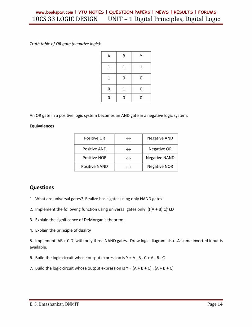
Truth table of OR gate (negative logic):
A B Y
1 1 1
1 0 0
0 1 0
0 0 0
An OR gate in a positive logic system becomes an AND gate in a negative logic system.
Equivalences
Positive OR ↔ Negative AND
Positive AND ↔ Negative OR
Positive NOR ↔ Negative NAND
Positive NAND ↔ Negative NOR
Questions
1. What are universal gates? Realize basic gates using only NAND gates.
2. Implement the following function using universal gates only: (((A + B).C)’).D
3. Explain the significance of DeMorgan’s theorem.
4. Explain the principle of duality
5. Implement AB + C’D’ with only three NAND gates. Draw logic diagram also. Assume inverted input is
available.
6. Build the logic circuit whose output expression is Y = A . B . C + A . B . C
7. Build the logic circuit whose output expression is Y = (A + B + C) . (A + B + C)
www.bookspar.com | VTU NOTES | QUESTION PAPERS | NEWS | RESULTS | FORUMS