
Type-II Dirac surface states in topological crystalline ... · Type-II Dirac surface states in...
14
Type-II Dirac surface states in topological crystalline insulators Ching-Kai Chiu, 1, 2, 3 Y.-H. Chan, 4 Xiao Li, 3 Y. Nohara, 5 and A. P. Schnyder 5 1 Department of Physics and Astronomy, University of British Columbia, Vancouver, BC, Canada V6T 1Z1 2 Quantum Matter Institute, University of British Columbia, Vancouver BC, Canada V6T 1Z4 3 Condensed Matter Theory Center and Joint Quantum Institute and Maryland Q Station, Department of Physics, University of Maryland, College Park, MD 20742, USA 4 Institute of Atomic and Molecular Sciences, Academia Sinica, Taipei 10617, Taiwan 5 Max-Planck-Institute for Solid State Research, Heisenbergstr. 1, D-70569 Stuttgart, Germany (ΩDated: June 16, 2016) We study the properties of a family of anti-pervoskite materials, which are topological crystalline insulators with an insulating bulk but a conducting surface. Using ab-initio DFT calculations, we investigate the bulk and surface topology and show that these materials exhibit type-I as well as type-II Dirac surface states protected by reflection symmetry. While type-I Dirac states give rise to closed circular Fermi surfaces, type-II Dirac surface states are characterized by open electron and hole pockets that touch each other. We find that the type-II Dirac states exhibit characteristic van-Hove singularities in their dispersion, which can serve as an experimental fingerprint. In addition, we study the response of the surface states to magnetic fields. Topological crystalline insulators (TCIs) are insulating in the bulk, but exhibit conducting boundary states protected by crystal symmetries [1–3]. As opposed to surface states of or- dinary insulators, the gapless modes at the surface of TCIs arise due to a non-trivial topology of the bulk wavefunctions, which is characterized by a quantized topological invariant, e.g., a mirror Chern or mirror winding number [4–6]. One prominent example of a TCI is the rocksalt semiconductor SnTe [7–10], which supports at its (001) surface four Dirac cones protected by reflection symmetries. The surface modes of this and all other known TCIs are of the standard Dirac fermion type with closed point-like (or circular) Fermi sur- faces, which we refer to as “type-I”. However, as we discuss in this article, crystal symmetries can also give rise to other types of surface fermions. In particular, we show that at certain surfaces of the anti-perovskite materials A 3 EO [11–16] there exist so called “type-II” Dirac points which are protected by reflection sym- metry. (Here A denotes an alkaline earth metal, while E stands for Pb or Sn.) These type-II band crossings do not lead to cir- cular Fermi surfaces, but rather give rise to open electron and hole pockets that touch each other. This is reminiscent of the type-II Weyl points that have recently been predicted to ex- ist in WTe 2 [17–20] and LaAlGe [21]. Here, however, these type-II band crossings occur at the surface rather than in the bulk of the material. As a consequence, the surface physics of A 3 EO is radically different to the one of standard TCIs with point-like Dirac surface states. This pertains in particular to the surface magneotransport. Using first-principles calculations and a tight-binding model, we systematically study the surface states of A 3 EO, with a particular focus on Ca 3 PbO, which crystallizes in its low-temperature phase in the cubic space group Pm ¯ 3m. We find that the (011) surface exhibits type-II Dirac nodes, whereas the (111) surface supports both type-I and type-II Dirac states. On the (001) surface, on the other hand, the Dirac nodes overlap with the bulk bands. All these surface states are protected by the crystal symmetries of A 3 EO, in particular the reflection symmetries. We show that the type- II Dirac nodes exhibit characteristic van Hove singularities in their dispersions, which can be used as an experimental finger- print. Moreover, we analyze the response of the surface states to a magnetic field and show how the Landau level spectra of type-II Dirac nodes radically differ from those of type-I Dirac states. In particular, we find that for type-II Dirac states there is a very large density of Landau levels near the energy of the Dirac point. Moreover, as opposed to type-I Dirac states, the type-II Dirac nodes do not exhibit a zeroth Landau level that is pinned to the energy of the Dirac band crossing. Results Before considering the detailed topology of the anti- perovskites A 3 EO, let us first present a general discussion of the types of fermions that can arise at the surface of topologi- cal (crystalline) insulators. Types of surface fermions. The Hamiltonian describing the low-energy physics of two-dimensional (2D) surface Dirac states is of the generic form H surf (k) = X i=1,2 α=0,1,2 k i A iα σ α , (1) where k i denote the two surface momenta, σ i are the Pauli matrices, and σ 0 represents the 2 × 2 identity matrix. The energy spectrum of H surf is given by E ± = X i k i A i0 ± v u t X j X i k i A ij 2 ≡ L(k) ± W(k), (2) where the sums are over i, j = 1, 2. The second term W(k) in Eq. (2) is the linear spectrum of standard (i.e., type-I) Dirac fermions. That is, for L(k) < W(k), the surface state is cate- gorized as type I. Since the energy of type-I Dirac states is dis- persive in all directions, we require that det(A ij ) , 0. On the other hand, if there exists one momentum direction k 0 , such that L(k 0 ) > W(k 0 ), we categorize the surface state as type II. This is in analogy to the three-dimensional (3D) type-II Weyl points, which have been recently discovered in WeTe 2 [17]. We note that, while 3D Wely points are stable in the absence of arXiv:1606.03456v2 [cond-mat.mes-hall] 15 Jun 2016
Transcript of Type-II Dirac surface states in topological crystalline ... · Type-II Dirac surface states in...

Type-II Dirac surface states in topological crystalline insulators
Ching-Kai Chiu,1, 2, 3 Y.-H. Chan,4 Xiao Li,3 Y. Nohara,5 and A. P. Schnyder5
1Department of Physics and Astronomy, University of British Columbia, Vancouver, BC, Canada V6T 1Z12Quantum Matter Institute, University of British Columbia, Vancouver BC, Canada V6T 1Z4
3Condensed Matter Theory Center and Joint Quantum Institute and Maryland Q Station,Department of Physics, University of Maryland, College Park, MD 20742, USA
4Institute of Atomic and Molecular Sciences, Academia Sinica, Taipei 10617, Taiwan5Max-Planck-Institute for Solid State Research, Heisenbergstr. 1, D-70569 Stuttgart, Germany
(ΩDated: June 16, 2016)
We study the properties of a family of anti-pervoskite materials, which are topological crystalline insulatorswith an insulating bulk but a conducting surface. Using ab-initio DFT calculations, we investigate the bulk andsurface topology and show that these materials exhibit type-I as well as type-II Dirac surface states protectedby reflection symmetry. While type-I Dirac states give rise to closed circular Fermi surfaces, type-II Diracsurface states are characterized by open electron and hole pockets that touch each other. We find that the type-IIDirac states exhibit characteristic van-Hove singularities in their dispersion, which can serve as an experimentalfingerprint. In addition, we study the response of the surface states to magnetic fields.
Topological crystalline insulators (TCIs) are insulating in thebulk, but exhibit conducting boundary states protected bycrystal symmetries [1–3]. As opposed to surface states of or-dinary insulators, the gapless modes at the surface of TCIsarise due to a non-trivial topology of the bulk wavefunctions,which is characterized by a quantized topological invariant,e.g., a mirror Chern or mirror winding number [4–6]. Oneprominent example of a TCI is the rocksalt semiconductorSnTe [7–10], which supports at its (001) surface four Diraccones protected by reflection symmetries. The surface modesof this and all other known TCIs are of the standard Diracfermion type with closed point-like (or circular) Fermi sur-faces, which we refer to as “type-I”. However, as we discussin this article, crystal symmetries can also give rise to othertypes of surface fermions.
In particular, we show that at certain surfaces of theanti-perovskite materials A3EO [11–16] there exist so called“type-II” Dirac points which are protected by reflection sym-metry. (Here A denotes an alkaline earth metal, while E standsfor Pb or Sn.) These type-II band crossings do not lead to cir-cular Fermi surfaces, but rather give rise to open electron andhole pockets that touch each other. This is reminiscent of thetype-II Weyl points that have recently been predicted to ex-ist in WTe2 [17–20] and LaAlGe [21]. Here, however, thesetype-II band crossings occur at the surface rather than in thebulk of the material. As a consequence, the surface physics ofA3EO is radically different to the one of standard TCIs withpoint-like Dirac surface states. This pertains in particular tothe surface magneotransport.
Using first-principles calculations and a tight-bindingmodel, we systematically study the surface states of A3EO,with a particular focus on Ca3PbO, which crystallizes inits low-temperature phase in the cubic space group Pm3m.We find that the (011) surface exhibits type-II Dirac nodes,whereas the (111) surface supports both type-I and type-IIDirac states. On the (001) surface, on the other hand, theDirac nodes overlap with the bulk bands. All these surfacestates are protected by the crystal symmetries of A3EO, inparticular the reflection symmetries. We show that the type-II Dirac nodes exhibit characteristic van Hove singularities in
their dispersions, which can be used as an experimental finger-print. Moreover, we analyze the response of the surface statesto a magnetic field and show how the Landau level spectra oftype-II Dirac nodes radically differ from those of type-I Diracstates. In particular, we find that for type-II Dirac states thereis a very large density of Landau levels near the energy of theDirac point. Moreover, as opposed to type-I Dirac states, thetype-II Dirac nodes do not exhibit a zeroth Landau level thatis pinned to the energy of the Dirac band crossing.
ResultsBefore considering the detailed topology of the anti-perovskites A3EO, let us first present a general discussion ofthe types of fermions that can arise at the surface of topologi-cal (crystalline) insulators.Types of surface fermions. The Hamiltonian describing thelow-energy physics of two-dimensional (2D) surface Diracstates is of the generic form
Hsurf(k) =∑i=1,2α=0,1,2
kiAiασα, (1)
where ki denote the two surface momenta, σi are the Paulimatrices, and σ0 represents the 2 × 2 identity matrix. Theenergy spectrum of Hsurf is given by
E± =∑
i
kiAi0 ±
√√√∑j
∑i
kiAi j
2
≡ L(k) ±W(k), (2)
where the sums are over i, j = 1, 2. The second term W(k) inEq. (2) is the linear spectrum of standard (i.e., type-I) Diracfermions. That is, for L(k) < W(k), the surface state is cate-gorized as type I. Since the energy of type-I Dirac states is dis-persive in all directions, we require that det(Ai j) , 0. On theother hand, if there exists one momentum direction k0, suchthat L(k0) > W(k0), we categorize the surface state as type II.This is in analogy to the three-dimensional (3D) type-II Weylpoints, which have been recently discovered in WeTe2 [17].We note that, while 3D Wely points are stable in the absence of
arX
iv:1
606.
0345
6v2
[co
nd-m
at.m
es-h
all]
15
Jun
2016

2
any symmetry (except translation), two-dimensional surfaceDirac states can only exist in the presence of time-reversalsymmetry or spatial symmetries, such as reflection.
Now, the interesting question is how these symmetries re-strict the form of Eq. (1). For a 3D time-reversal (TR) invari-ant strong topological insulator, the Hamiltonian HSTI satis-fies T HSTI(−k)T−1 = HSTI(k), with the time-reversal opera-tor T = σyK and the complex conjugation operator K. Thissymmetry locks the Dirac node at the time-reversal invariantpoints of the BZ, such as, e.g., k = 0. We observe that the lin-ear term kiσ0 is forbidden by time-reversal symmetry. Hence,the surface states of TR invariant strong topological insulatorsare described by
HSTI(k) = kyσx − kxσy, (3)
and are therefore always of type I.However, type-II Dirac fermions can appear at the surface
of reflection symmetric TCIs (and weak TR symmetric topo-logical insulators). The reflection symmetric Hamiltonian ofthese type-II surface states is generically given by
HsurfTCI(kx, ky) = Akyσ0 + kyσx − kxσy, (4)
with A > 1. (Without loss of generality we have set the Fermivelocities to 1 and assumed that the reflection plane is kx = 0.)The type-II Dirac state (4) is protected by reflection symmetryx→ −x, which acts on (4) as
RxHsurfTCI(−kx, ky)R−1
x = HsurfTCI(kx, ky), (5)
with the reflection operator Rx = σx. Since reflection flips thesign of kx, it allows the linear term Akyσ0 but forbids kxσ0.
The crucial difference between type-I and type-II Dirac sur-face states is that the former have closed circular Fermi sur-faces, whereas the latter exhibit open electron and hole pock-ets which touch each other. As one varies the Fermi energyEF , the Fermi surface of type-I Dirac states can be shrunk toa single point, which is called a type-I Dirac point. In con-trast, type-II Dirac states give rise to electron and hole pock-ets, whose size depends on the Fermi energy. At a certain EFthe electron and hole Fermi surfaces touch each other, whichis called a type-II Dirac point. As opposed to type-I Diracpoints, the density of states at type-II Dirac points remains fi-nite. In addition, we observe that in type-II Dirac states one ofthe two surface bands must bend over in order to connect bulkvalence and conduction bands. As a consequence, there is amaximum in the dispersion of the surface states. The lattergives rise to a van Hove singularity, which leads to a kink inthe surface density of states. This can be used as an experi-mental fingerprint of type-II Dirac states.
Topology of anti-perovskite materials. As an example ofa TCI with type-II Dirac surface states, we consider the cu-bic anti-perovskite materials A3EO with space group Pm3m(Table I). The crystal structure of A3EO is an inverse per-ovskite structure, where the oxygen atom O is surrounded oc-tahedrally by the alkaline earth metal atoms A [see Fig. 1(a)].We choose Ca3PbO as a generic representative of this mate-rials class. The bulk band structure of Ca3PbO displays six
tol. factor bulk gap topologyCa3PbO 0.999 ∼ 15 meV nontrivialCa3SnO 0.993 ∼ 5 meV nontrivialSr3PbO 0.978 ∼ 18 meV nontrivialSr3SnO 0.973 ∼ 7 meV nontrivialBa3PbO 0.962 ∼ 10 meV nontrivialBa3SnO 0.957 gapless –
TABLE I. Familiy of anti-perovskite materials with cubic spacegroup Pm3m. The tolerance (tol.) factor indicates the deviation fromthe ideal inverse perovskite structure [15]. The bulk gap values areobtained from ab-initio first principles calculation. The wavefunc-tion topology is determined by the mirror Chern numbers Cx0 , Cxπ ,and Cx,y (see Methods). We find that the topology is nontrivial, withCx0 = Cx,y = 2 and Cxπ = 0, for all compounds except for Ba3SnO.
Dirac cones, which are gapped by spin-orbit coupling. WhileCa3PbO is known to be a trivial TR invariant insulator [12](i.e., a trivial class AII insulator [3]), it has recently been ar-gued that reflection symmetries give rise to a nontrivial wave-function topology with non-zero mirror Chern numbers [16].
Let us now discuss in detail how the non-trivial topologyof A3EO arises due to reflection symmetry. First, we observethat the space group Pm3m possesses nine different reflectionsymmetries Ri which transform r = (x, y, z) as (see Fig. 1)
Rxr =(−x, y, z), Ry,±zr =(x,±z,±y), (6a)Ryr =(x,−y, z), Rz,±xr =(±z, y,±x), (6b)Rzr =(x, y,−z), Rx,±yr =(±y,±x, z). (6c)
By Fourier transforming into momentum space, we find thatthere are 12 mirror planes in the Brillouin zone (BZ), namely,ki = 0, π and ki = ±k j for i, j = x, y, z and i , j. For eachof these reflection planes we can define a mirror Chern num-ber [4, 5, 22]. However, due to the cubic rotational symme-tries, only 3 out of these 12 mirror invariants are independent.Without loss of generality, we choose as an independent setthe mirror Chern numbers Cx0 , Cxπ , and Cx,y that are definedfor the reflection planes kx = 0, kx = π, and kx = ky, respec-tively. Both first-principles calculations and low-energy ef-fective considerations show that for the cubic anti-perovskitesthe mirror Chern numbers take the values Cx0 = Cx,y = 2and Cxπ = 0 (see Methods and Table I). Thus, in total thereare nine nonzero mirror Chern numbers, i.e., Ci0 = Ci,± j = 2for i, j = x, y, z and i , j. As shown in Appendix B, thelow-energy description of A3EO is given by six gapped Diraccones. Within this low-energy model one finds that there ex-ists only one bulk gap term m which respects the reflectionsymmetries and which gaps out all six Dirac cones. The signof this gap opening term, sgn(m), determines the mirror Chernnumbers, i.e.,
Cx,y = sgn(m) + bx,y, Cx0 = 2 sgn(m) + bx, (7)
where bx,y and bx are the mirror Chern numbers of the “back-ground” bands, i.e., those filled bands that are not includedin the low-energy description of the bulk Dirac cones. Forthe cubic anti-perovskites we find that bx,y = 1 and bx = 0.

3
FIG. 1. Crystal symmetries and surface terminations. (a) Crystal structure of Ca3PbO. (b), (c) and (d) Surface Brillouin zones (BZs) forthe (001), (011), and (111) surfaces, respectively. For the (001) and (011) surfaces the surface BZs can be obtained from the bulk cubic BZsby projecting along the [001] and [011] directions, respectively. For the (111) surface BZ this is not possible. Nevertheless the symmetriesof the surface BZ follow from the projection of the bulk reflection planes [see panel (d)]. The brown shaded areas in panels (b), (c), and (d)indicate the bulk mirror planes. The lower panels show the different surface terminations. The crystal symmetries of the (001), (011), and(111) surfaces are described by the 2D space groups p4m, pmm, and p3m1, respectively.
Hence, Cx0 is always non-zero even if the sign of the gap termswitches.
Surface states. By the bulk-boundary correspondence, a non-trivial value of the mirror Chern numbers Ci0 (or Ci,± j) leadsto the appearance of Dirac states on those surfaces that are leftinvariant by the corresponding mirror symmetry Ri0 (or Ri,± j).That is, the value of Ci0 (or Ci,± j) indicates the number of left-and right-moving chiral modes in the surface BZ. These chi-ral surface modes are located within the mirror line ki = 0 (orki = ±k j) that is symmetric under the reflection operation Ri0
(or Ri,± j), see Fig. 1. Importantly, left- and right-moving sur-face chiral modes belong to opposite eigenspaces of the reflec-tion operators Ri0 (or Ri,± j), and therefore cannot hybridize,see Fig. 2. That is, the band crossing between the left- andright-moving modes is protected by reflection symmetry. De-pending on the surface orientation of A3EO, this band cross-ing corresponds to the Dirac point of a type-I surface state, thetouching of electron- and hole-pockets of a type-II Dirac state,or is completely hidden in the bulk bands. In the following,we discuss these three possibilities for the case of Ca3PbO.
Hidden Dirac nodes on the (001) surface. We start by ex-amining the Dirac states on the (001) surface for the Ca-Pbtermination [lower left panel in Fig. 1(b)]. Projecting the sym-metries of Pm3m along the (001) direction, one finds that thetwo-dimensional space group of the (001) surface is p4m [23].The wallpaper group p4m contains four reflection symmetries,i.e., Rx, Ry, Rx,+y, and Rx,−y [Fig. 1(b)]. In the surface BZ, thisgives rise to six mirror lines kx = 0, kx = π, ky = 0, ky = π, kx =
±ky with three independent mirror Chern numbers Cx0 , Cxπ ,and Cx,y. From the above analysis we find that Cx0 = Cy0 = 2and Cx,y = Cx,−y = 2, which leads to two pairs of left- andright-moving chiral modes within the mirror lines kx = 0,ky = 0 and kx = +ky, kx = −ky, respectively. The left- andright-moving chiral modes belong to reflection eigenspaceswith R = −1 and R = +1, respectively. This is clearly visiblein Fig. 2, which shows the surface density of states along thehigh-symmetry lines Γ→ X and Γ→ M, which correspond to
(a) (b)
+1
+1
1
1 +1 1
+1 1
FIG. 2. Density of states at the (001) surface. (a), (b) Surfacedensity of states along the high-symmetry lines Γ → X and Γ →
M of the (001) surface BZ, respectively, for the Pb-Ca termination[lower left panel in Fig. 1(b)]. The two high-symmetry directionscorrespond to the two inequivalent mirror lines of Fig. 1(b), i.e., ky =
0 and kx = ky. The spectrum along the mirror line ky = 0 [panel(a)] exhibits two right-moving chiral modes with mirror eigenvalueRy = +1 and two left-moving chiral modes with mirror eigenvalueRy = −1. Similarly, the spectrum along the mirror line ky = kx [panel(b)] shows two right-moving chiral modes with Rx,−y = +1 and twoleft-moving chiral modes with Rx,−y = −1. We observe that the Diracnodal points (i.e., the bandcrossings) for the upper chiral modes arehidden by the bulk bands. For the lower chiral modes there is noband crossing at all, since the modes are too far apart.
the mirror lines kx = 0 and kx = ky, respectively. Interestingly,the band crossing formed by the upper left- and right-movingchiral modes is completely hidden by the bulk bands. Thelower chiral modes, on the other hand, do not show a bandcrossing, since they are too far apart. Similar chiral modesalso appear for the Ca-O termination, see Fig. S4.Type-II Dirac nodes on the (011) surface. Next, we con-sider the Dirac states on the (011) surface, whose wallpapergroup is pmm. We focus here on the Ca-Pb-O termination;the results for the other termination are shown in Appendix D.The two-dimensional space group pmm contains two reflec-tion symmetries, Rx and Ry,z, see Fig. 1(c). Correspondingly,the (011) surface BZ exhibits two mirror lines, namely, kx = 0
4
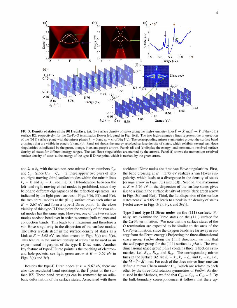
FIG. 3. Density of states at the (011) surface. (a), (b) Surface density of states along the high-symmetry lines Γ→ X and Γ→ Y of the (011)surface BZ, respectively, for the Ca-Pb-O termination [lower left panel in Fig. 1(c)]. The two high-symmetry lines represent the intersectionof the (011) surface plane with the mirror planes kx = 0 and ky = kz of Fig 1(c). The corresponding mirror symmetries protect the surface bandcrossings that are visible in panels (a) and (b). Panel (c) shows the energy resolved surface density of states, which exhibits several van Hovesingularities as indicated by the green, orange, blue, and purple arrows. Panels (d) and (e) display the energy- and momentum-resolved surfacedensity of states for different energy ranges. The van Hove singularities are marked by the arrows. Panel (f) shows the momentum-resolvedsurface density of states at the energy of the type-II Dirac point, which is marked by the green arrow.
and ky = kz, with the two non-zero mirror Chern numbers Cx0
and Cyz. Since Cx0 = Cyz = 2, there appear two pairs of left-and right-moving chiral surface modes within the mirror lineskx = 0 and ky = kz, see Fig. 3. Hybridization between theleft- and right-moving chiral modes is prohibited, since theybelong to different eigenspaces of the reflection operators. Asindicated by the light green arrows in Figs. 3(b), 3(f), and 3(e),the two chiral modes at the (011) surface cross each other atE = 5.67 eV and form a type-II Dirac point. In the closevicinity of this type-II Dirac point the velocity of the two chi-ral modes has the same sign. However, one of the two surfacemodes needs to bend over in order to connect bulk valence andconduction bands. This leads to a maximum and therefore avan Hove singularity in the dispersion of the surface modes.The latter reveals itself in the surface density of states as akink at E = 5.68 eV, see blue arrows in Figs. 3(c) and 3(e).This feature in the surface density of states can be used as anexperimental fingerprint of the type-II Dirac state. Anotherkey feature of type-II Dirac points is the touching of electron-and hole-pockets, see light green arrow at E = 5.67 eV inFigs. 3(e) and 3(f).
Besides the type-II Dirac nodes at E = 5.67 eV, there arealso two accidental band crossings at the Γ point of the sur-face BZ. These band crossings can be removed by an adia-batic deformation of the surface states. Associated with these
accidental Dirac nodes are three van Hove singularities. First,the band crossing at E = 5.75 eV realizes a van Hoves sin-gularity, which leads to a divergence in the density of states[orange arrow in Figs. 3(c) and 3(d)]. Second, the maximumat E = 5.76 eV in the dispersion of the surface states givesrise to a kink in the surface density of states [dark green arrowin Figs. 3(a) and 3(c)]. Third, the flat dispersion of the surfacestates near E = 5.65 eV leads to a peak in the density of states[violet arrow in Figs. 3(a), 3(c), and 3(e)].
Type-I and type-II Dirac nodes on the (111) surface. Fi-nally, we examine the Dirac states on the (111) surface forthe Ca-Pb termination. (We note that the surface states of theO termination are expected to be similar to the ones of theCa-Pb termination, since the oxygen bands are far away in en-ergy from the Fermi energy.) Projecting the three-dimensionalspace group Pm3m along the (111) direction, we find thatthe wallpaper group for the (111) surface is p3m1. The two-dimensional space group p3m1 contains three reflection sym-metries, i.e., Rx,y, Rx,z, and Ry,z. The corresponding mirrorlines in the surface BZ are kx = ky, kx = kz, and ky = kz, i.e.,the M− Γ− M lines. For each of the three mirror lines one candefine a mirror Chern number Ci, j, which are related to eachother by the three-fold rotation symmetries of Pm3m. As dis-cussed in the Methods, we find that Cx,y = Cx,z = Cy,z = 2. Bythe bulk-boundary correspondence, it follows that there ap-

5
FIG. 4. Density of states at the (111) surface. (a), (b) Surface density of states along the high-symmetry lines Γ → K and Γ → M of the(111) surface BZ, respectively, for the Ca-Pb termination. The Γ→ M direction corresponds to the mirror lines of the (111) surface. Thus, thespectrum along Γ → M is gapless and there appear two type-II Dirac states protected by reflection symmetry. The spectrum along the Γ − Kline, on the other hand, is gapped, since it is not a mirror line. (c) Surface density of states which exhibits several van Hove singularities asindicated by the orange, blue, and green arrows. The van Hove singularity at E = 5.76 eV (orange peak) stems from the back bending of thetype-II Dirac state. (d) Schematic illustration of the six type-II Dirac states on the (111) surface. (e), (f) Energy- and momentum-resolvedsurface density of states for different energy ranges. The van Hove singularities are indicated by the blue and orange arrows. The red arrowindicates the type-II Dirac point at E = 5.70 eV, where the electron and hole pockets meet.
pear two pairs of left- and right-moving chiral modes withinthe M − Γ − M lines of the surface BZ, see Fig. 4(b). Thesechiral bands cross each other at E = 5.70 eV, thereby formingtype-II Dirac points [red arrow in Fig. 4(b)]. Close to thesetype-II Dirac points, the velocities of the chiral modes havethe same sign. But further away, one of the two modes bendsover, such that it connects bulk valence and conduction bands.Hence, this surface band must exhibit a maximum [orange ar-rows in Figs. 4(b) and 4(e)], which leads to a van Hove singu-larity in the surface density of states at E = 5.76 eV [orangearrow in Fig. 4(c)]. Another key feature of this type-II Diracstate is the touching of the electron and hole Fermi surfaces.That is, with increasing Fermi energy the open electron andhole-pockets approach each other, touch at the type-II Diracpoint with E = 5.70 eV [red arrow in Fig. 4(f)], and then sep-arate again.
In addition to these type-II Dirac nodes, the (111) sur-face also exhibits two accidental type-I Dirac nodes at theΓ point, which can be removed by adiabatic transformations.Connected to these accidental Dirac nodes are two van Hovesingularities. First, the Dirac point at E = 5.81 eV repre-sents a saddle-point van Hove singularity, which leads to alog divergence in the surface density of states [green arrowsin Figs. 4(b) and 4(c)]. Second, the lower bands of theDirac state at E = 5.81 eV bend over, forming a minimumat E = 5.78 eV. This leads to a kink in the surface density ofstates [blue arrow in Figs. 4(a) and 4(c)].
Landau level spectrum. A drastic difference between type-Iand type-II Dirac surface states arises when a magnetic fieldis applied. For type-I Dirac cones the energy spectrum of theLandau levels is given by
En ∼√
n, (8)
where n is the Landau level index. Hence, the Landau lev-els of type-I Dirac cones are in general well separated. Thisis in contrast to type-II Dirac cones. To illustrate this, let usconsider the following tight-binding model on a square lat-tice [24],
H = −∑〈i j〉
ti jb†
jai + t1∑〈i j〉
(a†jai + b†jbi
), (9)
where ai and bi denote the electron annihilation operators onthe sublattice A and B, respectively. ti j represent the near-est neighbor hopping, while t1 is the next nearest neighborhopping integral (for more details see Appendix C). Hamilto-nian (9) describes two Dirac cones, whose tilting is controlledby the ratio t1/t, with t =
∣∣∣ti j
∣∣∣. For t1/t = 0 there is no tilting[Fig. 5(a)] and for t1/t = 0.2 there is a small tilting [Fig. 5(b)].In both cases there exist well separated Landau levels. (Notethat the dispersive curves in the Landau level structure aredue to edge states and therefore should be ignored in the fol-lowing discussion.) At t1/t = 1/2 there is a transition fromtype-I Dirac states to type-II Dirac states. At this transition

6
-2 -1 0 1 2-1
-0.5
0
0.5
1-2 -1 0 1 2
-1
-0.5
0
0.5
1
-2 -1 0 1 2-1
-0.5
0
0.5
1
-2 -1 0 1 2-1
-0.5
0
0.5
1
(a)E
k/t
ak2 ak2
(b)
Ek/t
(c)
(d)
Ek/t
Ek/t
FIG. 5. Landau level spectrum for type-I and type-II Diracsurface states. The left and right columns show the energy spec-trum and Landau level structure, respectively, for the tight-bindingmodel given by Eq. (9). The magnetic field strength is chosen to beB = 0.01φ0/a2, where φ0 ≡ h/e is the flux quantum and a2 is theare of a plaquette of the square lattice, see Fig. S2. The tilting of theDirac cones is controlled by the ratio t1/t. The four rows correspondto (a) t1/t = 0 (type-I Dirac cone), (b) t1/t = 0.2 (type-I Dirac cone),(c) t1/t = 0.5 (transition between type-I and -II Dirac cones), and (d)t1/t = 0.6 (type-II Dirac cone), respectively. All dispersive curves inthe Landau level structure arise from states localized at the edge ofthe sample, and thus are not of interest here.
point the spectrum becomes nondispersive along the k2 direc-tion and the Landau levels get very dense around E = 0 (i.e.,around the energy of the Dirac point) [Fig. 5(c)]. Finally, fort1/t > 1/2, there appear type-II Dirac cones with open elec-tron and hole pockets. As shown in Fig. 5(d), for type-II Diraccones the separation between the Landau levels near E = 0 isclose to zero, leading to a sizable region of very dense Landaulevels [cf. Fig. 5(d)]. This region of dense Landau levels arisesbecause the open electron and hole Fermi surfaces enclose avery large momentum-space area, which is much larger thanthe one enclosed by type-I Dirac states (for a detailed expla-nation, see Appendix C). Moreover, we find that for type-IIDirac states the zeroth Landau level E0 of the type-I Diracnode [see Figs. 5(a) and 5(b)] becomes unpinned and movesaway from E = 0.
DiscussionUsing general symmetry arguments, we have shown that thesurface of crystalline topological insulators can host type-II
Dirac surface states, which are characterized by open elec-tron and hole Fermi surfaces that touch each other. This isin contrast to regular strong topological insulators, where theDirac surface states, due to time-reversal symmetry, are al-ways of type-I, which exhibit a closed small Fermi surface. Bymeans of ab-initio DFT calculations, we have demonstratedthat type-II Dirac states appear at the surfaces of the antiper-ovskite materials A3EO. As a representative example, we haveconsidered Ca3PbO and determined the surface spectra for the(001), (011), and (111) surfaces. The type-II Dirac nodes ap-pear on the (011) surface with Ca and Ca-Pb-O terminations,and on the (111) surface with Ca-Pb termination (see Figs. 3and 4). All these band crossings are protected by reflectionsymmetry. That is, the left moving and right moving chiralmodes that cross each other belong to different eigenspaces ofthe reflection operator R. We have shown that type-II Diracsurface states possess van Hove singularities, since one of thetwo chiral modes needs to bend over in order to connect va-lence with conduction bands. These van Hove singularitieslead to divergences and kinks in the surface density of states,which can serve as unique fingerprints of the type-II Diracstates. Another distinguishing feature of type-II Dirac statesis their Landau level spectrum. As opposed to type-I Diracstates, where the Landau levels are well separated, for type-IIDirac states there exists a very large density of Landau lev-els near the band-crossing energy (see Fig. 5). It will be in-teresting to compare these theoretical findings with quantumoscillations [25], angle-resolved photoemission, and scanningtunneling experiments.
Using a low-energy theory and a DFT-derived tight-bindingmodel, we have determined the mirror Chern numbers for thecubic antiperovskites. We have shown that the mirror Chernnumbers for the ki = 0 and ki = ±k j (for i, j = x, y, z andi , j) mirror planes are equal to two, indicating that thereappear two left- and right-moving modes on surfaces that areinvariant under the mirror symmetries. Depending on the sur-face orientation and termination these left- and right-movingmodes form type-I or type-II Dirac nodes, or do not cross atall. We remark that while the mirror Chern numbers deter-mine the number of left- and right-moving chiral modes thatconnect valence and conduction bands, they do not give anyinformation about the number of Dirac band crossings in thesurface spectrum. This is because, (i) the Dirac points mightbe hidden in the bulk, (ii) the left- and right-moving modesmight be too far apart to form a crossing, or (iii) there mightbe accidental band crossings.
Methods
DFT calculations and tight-binding model. The electronicband structure of the cubic antiperovskites A3EO is deter-mined by performing first-principles calculations with the Vi-enna ab initio package [26, 27] using the projector augmentedwave (PAW) method [28, 29]. As an input for the DFT calcu-lation we used the experimental crystal structure of Ref. [15].The lattice constant for Ca3PbO is 4.847 Å. For the exchange-correlation functional we chose the generalized-gradient ap-proximation of Perdew-Burke-Ernzerhof type [30]. The plane
7
wave basis is truncated with an energy cut-off of 400 eV. Forthe bulk calculation a 12 × 12 × 12 k-mesh is used. Spin-orbitcoupling effects are also taken into account.
The DFT calculations show that near the Fermi energy EFthe valence bands mostly originate from Pb-p orbitals (px, py,and pz), while the orbital character of the conduction bandsnear EF is Ca-dx2−y2 , Ca-dxz, and Ca-dyz (from three differentCa atoms). Guided by these findings, we use these 12 orbitals(24 including spin) as a basis set to derive a low-energy tight-binding model. We determine the hopping parameter valuesfor this tight-binding model from a maximally localized Wan-nier function (MLWF) method [31, 32]. With this model, wecompute the momentum-resovled surface density of states bymeans of an iterative Green’s function method [33]. The re-sults of these calculations are shown in Figs. 2, 3, and 4. Todetermine the topological characteristics of Ca3PbO we havealso used a simplified nine-band (18 bands including spin)tight-binding model, see Appendix A for details.
Topological invariants. The type-I and type-II Dirac surfacestates of the cubic antiperovskites are protected by a mirrorChern number. The mirror Chern number is defined as atwo-dimensional integral over the reflection plane of the oc-cupied wave functions with mirror eigenvalue R = +1 (orR = −1) [2, 8]. Note that since the Hamiltonian H commuteswith the reflection operator, the eigenfunctions of H can be as-signed a definite mirror eigenvalue. Without loss of generality,one usually assumes that the mirror eigenvalues are ±1, sinceR2 = 1 after a suitable U(1) gauge transformation [4]. Thevalue of the mirror Chern number corresponds to the numberof left- and right-moving chiral surface modes. These chiralsurface modes exist within the mirror line of the surface BZ,i.e., within the line that is obtained by projecting the bulk mir-ror plane onto the surface BZ.
We have numerically computed the mirror Chern num-ber using two different methods: (i) using the simpli-fied tight binding model of Appendix A and (ii) using thereal space wavefunctions of the DFT-derived 12-band tight-binding model. For method (i) the reflection operator R can be
written explicitly in momentum space. The momentum spaceHamiltonian can then be block diagonalized with respect to Rand the eigenfunctions can be obtained for each block sep-arately (see Appendix A for details). For method (ii) thereal-space wavefunctions of the 12-band tight-binding modelare projected onto the mirror eigenspaces (1 ± R)/2. This isdone by identifying mirror-reflected orbitals with proper signchanges. Using these projected wavefunctions a Fourier trans-form is performed along the two surface momenta to obtainthe surface spectrum for a given reflection eigenspace. TheChern number can then be inferred from the number of chiralsurface modes in the surface spectrum. Both methods (i) and(ii) agree with each other.
AcknowledgementsWe gratefully acknowledge many useful discussions withM. Y. Chou, M. Franz, M. Hirschmann, H. Nakamura,J. Nuss, A. Rost, and H. Takagi. C.K.C. would like to thankthe Max-Planck-Institut FKF Stuttgart for its hospitality andacknowledge the support of the Max-Planck-UBC Centrefor Quantum Materials and Microsoft. X.L. and C.K.C. aresupported by LPS-MPO-CMTC. Y.H.C. is supported by aThematic project at Academia Sinica.
Competing financial interestsThe authors declare that they have no competing financial in-terests.
Author contributionsY.H.C. and Y.N. performed the ab-initio first-principles calcu-lations. All authors contributed to the discussion and interpre-tation of the results and to the writing of the paper.
Data availabilityAll relevant numerical data are available from the authorsupon request.
[1] Y. Ando and L. Fu, Annual Review of Condensed MatterPhysics, Annual Review of Condensed Matter Physics (2014).
[2] J. C. Y. Teo, L. Fu, and C. L. Kane, Phys. Rev. B 78, 045426(2008).
[3] C.-K. Chiu, J. C. Y. Teo, A. P. Schnyder, and S. Ryu, ArXive-prints (2015), arXiv:1505.03535 [cond-mat.mes-hall].
[4] C.-K. Chiu, H. Yao, and S. Ryu, Phys. Rev. B 88, 075142(2013).
[5] T. Morimoto and A. Furusaki, Phys. Rev. B 88, 125129 (2013).[6] K. Shiozaki and M. Sato, Phys. Rev. B 90, 165114 (2014).[7] P. Dziawa, B. J. Kowalski, K. Dybko, R. Buczko, A. Szczer-
bakow, M. Szot, E. Łusakowska, T. Balasubramanian, B. M.Wojek, M. H. Berntsen, O. Tjernberg, and T. Story, Nat. Mater.11, 1023 (2012).
[8] T. H. Hsieh, H. Lin, J. Liu, W. Duan, A. Bansil, and L. Fu, Nat.Commun. 3, 982 (2012).
[9] Y. Tanaka, Z. Ren, T. Sato, K. Nakayama, S. Souma, T. Taka-
hashi, K. Segawa, and Y. Ando, Nat. Phys. 8, 800 (2012).[10] S.-Y. Xu, C. Liu, N. Alidoust, M. Neupane, D. Qian, I. Belopol-
ski, J. D. Denlinger, Y. J. Wang, H. Lin, L. A. Wray, G. Landolt,B. Slomski, J. H. Dil, A. Marcinkova, E. Morosan, Q. Gibson,R. Sankar, F. C. Chou, R. J. Cava, A. Bansil, and M. Z. Hasan,Nat Commun 3, 1192 (2012).
[11] T. Kariyado and M. Ogata, J. Phys. Soc. Jpn. 80, 083704 (2011).[12] T. Kariyado and M. Ogata, J. Phys. Soc. Jpn. 81, 064701 (2012).[13] Y. Fuseya, M. Ogata, and H. Fukuyama, J. Phys. Soc. Jpn. 81,
013704 (2012).[14] T. Kariyado, Three-Dimensional Dirac Electron Systems in the
Family of Inverse-Perovskite Material Ca3PbO , Ph.D. thesis,The University of Tokyo, Tokyo (2012).
[15] J. Nuss, C. Muhle, K. Hayama, V. Abdolazimi, and H. Takagi,Acta Crystallographica Section B 71, 300 (2015).
[16] T. H. Hsieh, J. Liu, and L. Fu, Phys. Rev. B 90, 081112 (2014).[17] A. A. Soluyanov, D. Gresch, Z. Wang, Q. Wu, M. Troyer,

8
X. Dai, and B. A. Bernevig, Nature 527, 495 (2015).[18] L. Muechler, A. Alexandradinata, T. Neupert, and R. Car,
ArXiv e-prints (2016), arXiv:1604.01398.[19] C. Wang, Y. Zhang, J. Huang, S. Nie, G. Liu, A. Liang,
Y. Zhang, B. Shen, J. Liu, C. Hu, Y. Ding, D. Liu, Y. Hu,S. He, L. Zhao, L. Yu, J. Hu, J. Wei, Z. Mao, Y. Shi, X. Jia,F. Zhang, S. Zhang, F. Yang, Z. Wang, Q. Peng, H. Weng,X. Dai, Z. Fang, Z. Xu, C. Chen, and X. J. Zhou, ArXiv e-prints (2016), arXiv:1604.04218 [cond-mat.mes-hall].
[20] Y. Wu, N. H. Jo, D. Mou, L. Huang, S. L. Bud’ko,P. C. Canfield, and A. Kaminski, ArXiv e-prints (2016),arXiv:1604.05176.
[21] S.-Y. Xu, N. Alidoust, G. Chang, H. Lu, B. Singh, I. Belopol-ski, D. Sanchez, X. Zhang, G. Bian, H. Zheng, M.-A. Husanu,Y. Bian, S.-M. Huang, C.-H. Hsu, T.-R. Chang, H.-T. Jeng,A. Bansil, V. N. Strocov, H. Lin, S. Jia, and M. Zahid Hasan,ArXiv e-prints (2016), arXiv:1603.07318.
[22] C.-K. Chiu and A. P. Schnyder, Phys. Rev. B 90, 205136 (2014).[23] X.-Y. Dong and C.-X. Liu, Phys. Rev. B 93, 045429 (2016).[24] T. Kawarabayashi, Y. Hatsugai, T. Morimoto, and H. Aoki,
Phys. Rev. B 83, 153414 (2011).[25] A. W. Rost et al., to be published.[26] G. Kresse and J. Furthmuller, Phys. Rev. B 54, 11169 (1996).[27] G. Kresse and J. Furthmuller, Computational Materials Science
6, 15 (1996).[28] P. E. Blochl, Phys. Rev. B 50, 17953 (1994).[29] G. Kresse and D. Joubert, Phys. Rev. B 59, 1758 (1999).[30] J. P. Perdew, K. Burke, and M. Ernzerhof, Phys. Rev. Lett. 77,
3865 (1996).[31] A. A. Mostofi, J. R. Yates, Y.-S. Lee, I. Souza, D. Vanderbilt,
and N. Marzari, Computer Physics Communications 178, 685(2008).
[32] N. Marzari, A. A. Mostofi, J. R. Yates, I. Souza, and D. Van-derbilt, Rev. Mod. Phys. 84, 1419 (2012).
[33] M. P. L. Sancho, J. M. L. Sancho, J. M. L. Sancho, and J. Rubio,Journal of Physics F: Metal Physics 15, 851 (1985).
[34] A. Kobayashi, S. Katayama, Y. Suzumura, and H. Fukuyama,J. Phys. Soc. Japan 76, 1 (2007).
[35] M. O. Goerbig, J.-N. Fuchs, G. Montambaux, and F. Piechon,Phys. Rev. B 78, 045415 (2008).
[36] T. Morinari, T. Himura, and T. Tohyama, J. Phys. Soc. Japan78, 023704 (2009).
[37] M. O. Goerbig, J.-N. Fuchs, G. Montambaux, and F. Piechon,Euro. Phys. Lett. 85, 57005 (2009).
[38] T. Morinari and T. Tohyama, J. Phys. Soc. Japan 79, 044708(2010).
[39] Y. Hatsugai, T. Kawarabayashi, and H. Aoki, Phys. Rev. B 91,085112 (2015).
[40] I. Proskurin, M. Ogata, and Y. Suzumura, Phys. Rev. B 91,195413 (2015).
[41] X. Li, F. Zhang, and A. H. MacDonald, Phys. Rev. Lett. 116,026803 (2016).
[42] D. Xiao, Q. Niu, and M.-C. Chang, Rev. Mod. Phys. 82, 1959(2010).
[43] Y. Gao and Q. Niu, arXiv:1507.06342.

9
Supplementary Information for
“Type-II Dirac surface states in topologicalcrystalline insulators”
Authors: Ching-Kai Chiu, Y.-H. Chan, Xiao Li, Y. Nohara,and A. P. Schnyder
In this supplementary information we present the details ofthe simplified nine-band tight-binding model, a low-energyeffective theory of the cubic antiperovskites, their Landaulevel structure, and the surface state spectra for some addi-tional surface terminations.
Appendix A: Simplified tight-binding model of Ca3PbO
To construct a simplified tight-binding model we followalong the lines of the work by Kariyado and Ogata [12]. InRef. [12] a six-band model with the orbitals
Pbpx ,Pbpy ,Pbpz ,Ca1dy2−z2
,Ca2dz2−x2
, and Ca3dx2−y2
was constructed. This six-band model exhibits six gaplessDirac nodes along the Γ − X direction, but does not containa Dirac mass gap, which is present in the DFT calculations.To open up a gap one needs to include in addition the Ca1-dyz, Ca2-dzx, and Ca3-dxy orbitals. As we show below, thespin-orbit coupling between these orbitals and the Ca1-dy2−z2 ,Ca2-dz2−x2 , and Ca3-dx2−y2 orbitals represents a mass term, thatopens up a gap at the six Dirac cones. We use this nine-bandmodel to analyze the topological properties of Ca3PbO (andother cubic antiperovskites) and to compute the mirror Chernnumbers.
Thus, in the absence of spin-orbit coupling our tight-binding Hamiltonian is written as H =
∑k ψ†
kHk/2(k)ψk withthe ninne-component spinor
ψk = (Pbpx , Pbpy , Pbpz ,
Ca1dy2−z2
, Ca2dz2−x2
, Ca3dx2−y2
,
Ca1dyz, Ca2
dzx, Ca3
dxy)T
and the 9 × 9 matrix Hk/2, which can be expressed in blockform as
Hk/2(k) =
Hp Vu
dp V ldp
Vudp† Hu
d 0
V ldp† 0 Hl
d
. (A1)
The blocks of Hk/2(k) are given by
Hp =
ep − 2tppc2x 0 00 ep − 2tppc2y 00 0 ep − 2tppc2z
(A2)
and
Hud =
ed −4tddcxcy −4tddczcx−4tddcxcy ed −4tddcycz−4tddczcx −4tddcycz ed
and Hl
d = ed13, with 13 the 3×3 identity matrix. The couplingterms between p and d orbitals are
Vudp = 4itpd
0 czsx −cysx−czsy 0 cxsycysz −cxsz 0
, V ldp = 4itpd
0 cxsz cxsycysz 0 cysxczsy czsx 0
,(A3)
where we have used the short-hand notation
ci = coski
2, si = sin
ki
2, c2i = cos ki.
In order to simplify matters, we have neglected in the aboveexpressions further neighbor hopping terms that were in-cluded in the work by Kariyado and Ogata [12]. We havechecked that these simplifications do not alter the topologicalproperties.
Let us now add spin-orbit coupling terms to the Hamilto-nian (A1). The on-site spin-orbit coupling for the Pb-p or-bitals is given by
∑k ψ†p(k)Hp
SO(k)ψp(k) with the spinor
ψp(k) = (Pb↑px,Pb↑py
,Pb↑pz,Pb↓px
,Pb↓py,Pb↓pz
)
and
HpSO(k) =
λp
2
0 −i 0 0 0 1i 0 0 0 0 −i0 0 0 −1 i 00 0 −1 0 i 00 0 −i −i 0 01 i 0 0 0 0
.
The on-site spin-orbit coupling for the d orbitals reads∑k ψ†
d(k)HdSO(k)ψd(k) with the spinor
ψd(k) =
(Ca1,↑dy2−z2
,Ca2,↑dz2−x2
,Ca3,↑dx2−y2
,Ca1,↓dy2−z2
,Ca2,↓dz2−x2
,Ca3,↓dx2−y2
,
Ca1,↑dyz,Ca2,↑
dzx,Ca3,↑
dxy,Ca1,↓
dyz,Ca2,↓
dzx,Ca3,↓
dxy, )T ,
and
HdSO(k) =λdτy ⊗
σx ⊗
1 0 00 0 00 0 0
+ σy ⊗
0 0 00 1 00 0 0
+ σz ⊗
0 0 00 0 00 0 1
, (A4)
where τβ and σα represent d-orbital (x2i − x2
j and xix j) and spin(up and down) degree of freedom, respectively. As it turns outHd
SO(k) gaps out the bulk Dirac cones.Adding these spin-orbit coupling terms to Eq. (A1), we ob-
tain the full Hamiltonian
Hk/2tot (k) =
(Htot
p (k) Vtot(k)V†tot(k) Htot
d (k)
), (A5)

10
with
Htotp (k) =
(Hp 00 Hp
)+ Hp
SO(k),
Htotd (k) =
(σ0 ⊗ Hu
d 00 σ0 ⊗ Hl
d
)+ Hd
SO(k),
and
Vtot(k) =(σ0 ⊗ Vu
dp σ0 ⊗ V ldp
).
Note that the outermost grading of Htotp and σ0 in the above
expressions corresponds to the spin grading. The parametersof the above tight-binding model can be determined by fittingto the DFT results. We have used the following values (inunits of eV)
ep = 0.0, ed = 2.0, tpp = −0.4,tdd = −0.4, tpd = −0.4, λp = 0.75, λd = 0.1.
We have checked that the nine-band model Hamiltonian (A5)exhibits qualitatively the same surface states as the DFT-derived twelve-band model (cf. Fig. 2).
Let us now compute the mirror Chern numbers for thismodel. To this end, we first need to determine the reflec-tion operators. To remove fractional momenta in the symme-try operators, we first perform a unitary transformation on theHamiltonian (A5), i.e.,
Hk(k) = U†Hk/2tot (k)U, (A6)
where U = diag(Up,Udu,Udl
), with
Up = e−i(kx+ky+kz)/216, (A7)
Uud = U l
d = σ0 ⊗
e−ikx/2 0 0
0 e−iky/2 00 0 e−ikz/2
. (A8)
The reflection operator Rx for the mirror symmetry kx → −kxis given by
URx (k) =
Rp
x 0 00 Rdu
x 00 0 Rdl
x
, (A9)
where
Rpx =σx ⊗
−1 0 00 1 00 0 1
,Rdu
x =σx ⊗
1 0 00 eikx 00 0 eikx
,Rdl
x =σx ⊗
1 0 00 −eikx 00 0 −eikx
. (A10)
The expression of the reflection operator Rx,−y for the mirrorsymmetry (kx, ky)→ (−ky,−kx) reads
URx,−y (k) =
Rp
x,−y 0 00 Rdu
x,−y 00 0 Rdl
x,−y
, (A11)
where
Rpx,−y = −
σx + σy√
2⊗
0 1 01 0 00 0 −1
,Rdu
x,−y = −σx + σy√
2⊗
0 eikx 0eiky 0 00 0 ei(kx+ky)
,Rdl
x,−y = −σx + σy√
2⊗
0 eikx 0eiky 0 00 0 −ei(kx+ky)
. (A12)
These two reflection symmetries act on the Hamiltonian (A6)as
Hk(k) =U†RxHk(−kx, ky, kz)URx , (A13)
Hk(k) =U†Rx,−yHk(−ky,−kx, kz)URx,−y . (A14)
Due to these two mirror symmetries, the bulk wave functionsof Hk(k) in the mirror planes kx = 0 and kx = −ky, respec-tively, can be labelled by the mirror eigenvalues ±1. Withinthese two-dimensional mirror planes in momentum space, onecan compute the Chern number n±1 of the occupied bands foreach mirror eigenvalue separately. The mirror Chern num-ber is then given by C = (n+1 − n−1)/2. Using this approachwe have computed the mirror Chern numbers for Hk(k). Wefind that they are consistent with the number of chiral surfacemodes as computed from the DFT-derived twelve-band tight-binding model.
Appendix B: Low-energy effective theory
In this section we study the topology of the cubic antiper-ovskites A3EO using a low-energy effective theory. As dis-cussed in the main text, the surface states of A3EO are pro-tected by the nine reflection symmetries
Rkx k =(−kx, ky, kz), Rky,±kz k =(kx,±kz,±ky), (B1a)
Rky k =(kx,−ky, kz), Rkz,±kx k =(±kz, ky,±kx), (B1b)
Rkz k =(kx, ky,−kz), Rkx,±ky k =(±ky,±kx, kz), (B1c)
and the bulk band structure of A3EO exhibits six Dirac cones,which are gapped out by spin-orbit coupling. These six Diraccones are located on the Γ−X high-symmetry lines of the bulkBrillouin zone, i.e., at
k = (±∆, 0, 0), (0,±∆, 0), (0, 0 ± ∆). (B2)
In the absence of spin-orbit coupling, the low-energy physicsnear these six Dirac cones is described by the Hamilto-nian [12]
11
H(k) =
(kx ± ∆)σx ⊗ σz + kyσy ⊗ σz + kzσz ⊗ σz, near k = (∓∆, 0, 0)kxσx ⊗ σz + (ky ± ∆)σy ⊗ σz + kzσz ⊗ σz, near k = (0,∓∆, 0)kxσx ⊗ σz + kyσy ⊗ σz + (kz ± ∆)σz ⊗ σz, near k = (0, 0,∓∆)
. (B3)
We observe that Eq. (B3) is invariant under the nine mirrorsymmetries (B1). That is, the Hamiltonian H(k) obeys
U−1# H(k)U# = H(R#k) (B4)
with the symmetry operators Uki = σi ⊗ σx and Uki,±k j =σi∓σ j√
2⊗ σx. Moreover, we note that the six gapless Dirac
cones of Eq. (B3) are located within the mirror planes ki = 0(i = x, y, z). Hence, in order to compute the mirror Chernnumber for these mirror planes, the Dirac nodes need to begapped out, which occurs due to spin-orbit coupling. Withinthe low-energy model (B3), we find that there exists only onesymmetry-preserving gap opening term, namely m1⊗σx, withm a constant that is independent of k. The mass term m1⊗σxgaps out all six Dirac nodes. As we will see, this turns thesystem into a non-trivial topological crystalline insulator. Toshow this we need to determine the mirror Chern numbers.
Let us first consider the mirror Chern number in the kz = 0reflection plane. The eigenspace of Ukz with mirror eigen-value +1 is spanned by |ψ1〉 = (1, 1, 0, 0)/
√2 and |ψ2〉 =
(0, 0, 1,−1)/√
2. Projecting the low-energy Hamiltonian (B3)within the reflection plane kz = 0 onto this eigenspace gives
h(k)kz =
(kx ± ∆)σx + kyσy + mσz, near (∓∆, 0, 0),kxσx + (ky ± ∆)σy + mσz, near (0,∓∆, 0).
(B5)
We observe that the four Dirac cones, which are located withinthe mirror plane kz = 0 are gapped out by the same mass termmσz. Since all four Dirac cones have the same orientation, asign change in m leads to a Chern number change by +1 forall of the four Dirac cones (or −1 for all the four Dirac cones).Hence, the total mirror Chern number Cz0 changes by four,when m→ −m.
Second, we consider the mirror Chern number in thekx = −ky reflection plane. The eigenspace of Ukx,−ky withmirror eigenvalue +1 is spanned by the vectors |φ1〉 =
(e−iπ/8, 0, 0, eiπ/8)/√
2 and |φ2〉 = (0, e−iπ/8, eiπ/8, 0)/√
2. Pro-jecting Hamiltonian (B3) within the reflection plane kx = −kyonto this eigenspace yields
h(k)kx,+ky = kxyσy +(kz±∆)σz +mσx, near (0, 0,∓∆), (B6)
where kxy = (−kx + ky)/√
2. Because the two Dirac conesin Eq. (B6) have the same orientation, the total mirror Chernnumber Cx,y changes by two, when m→ −m.
From these observations, we conclude that the total mirrorChern numbers are given by
Ci0 = 2 sgn(m) + bi, Ci,± j = sgn (m) + bi,± j, (B7)
where bi and bi,± j are the mirror Chern numbers of the “back-ground” bands, i.e., those filled bands that are not included in
the low-energy description (B3). We note that there exists thefollowing relation between bi and bi,± j
bi − bi,± j = 1 mod 2. (B8)
This is because the number of chiral left- (or right-) movingsurface modes on the ki = 0 and ki = ±k j high symmetry linescan only differ by a multiple of two. That is, the surface modeson the ki = 0 line are continuously connected to the surfacemodes on the ki = ±k j line. The only way how the number ofchiral left- (or right-) moving modes can differ on these twohigh-symmetry lines is if left- (or right-) moving modes aregapped out pairwise.
Using the DFT-derived twelve-band tight-binding modeland the simplified nine-band model, we find that bi = 0 andbi,± j = 1. Hence, Ci0 = 2 sgn(m) and Ci,± j = sgn (m) + 1,which is in agreement with the results of Ref. [16].
Appendix C: Landau levels of tilted Dirac cones
In this section we study the Landau level spectra of type-IIDirac surface states. We note that the Landau level structureof tilted Dirac fermions has been studied previously in the lit-erature [24, 34–40], in the context of strained graphene andcertain organic conductors, like α-(BEDT-TTF)2I3. In thissection we first review the properties of Landau level spec-tra of titled type-I Dirac cones, and then extend these resultsto type-II Dirac surface states.
1. Effective model approach
We start by considering a toy model describing a tiltedDirac cone. The Hamiltonian of this model is given by
H0 = vF(ηπyσ0 + πxσx + πyσy), (C1)
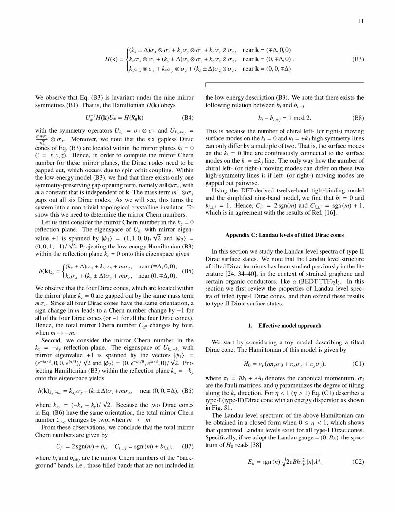
where πi = ~ki + eAi denotes the canonical momentum, σiare the Pauli matrices, and η parametrizes the degree of tiltingalong the ky direction. For η < 1 (η > 1) Eq. (C1) describes atype-I (type-II) Dirac cone with an energy dispersion as shownin Fig. S1.
The Landau level spectrum of the above Hamiltonian canbe obtained in a closed form when 0 ≤ η < 1, which showsthat quantized Landau levels exist for all type-I Dirac cones.Specifically, if we adopt the Landau gauge = (0, Bx), the spec-trum of H0 reads [38]
En = sgn (n)√
2eB~v2F |n| λ
3, (C2)
12
ky (a.u.)
Ener
gy(a
.u.)
-1.0 -0.5 0.0 0.5 1.0-3
-2
-1
0
1
2
3
FIG. S1. Comparison between a type-I (dashed lines) and a type-II (solid lines) Dirac fermion. Shown are the energy dispersions ofEq. (C1) with η = 0.5 (type-I) and η = 2 (type-II). The valencebands are marked by yellow and light blue for type-I and type-IIDirac fermions, respectively.
where λ =√
1 − η2, and n is the Landau level index. Oneintuitive way to understand why Landau level-like spectrastill persists for a tilted Dirac cone with 0 ≤ η < 1 is thatall constant-energy contours in the momentum space are stillclosed loops, although with an anisotropic shape [41]. As aresult, quantized Landau levels can be derived within a semi-classical picture [42]. Mathematically, the reason for the ex-istence of quantized Landau levels is that the correspondingeigenvalue problem H0Φ(r) = EΦ(r) can be mapped to theproblem of a one-dimensional harmonic oscillator, as long as0 ≤ η < 1. Specifically, the eigenstates are governed by thefollowing differential equation [38],− d2
dX2 + (1 − η2)(X +
η
1 − η2 ε
)2 φ(X)
=
ε2
1 − η2 − 1 iη
iηε2
1 − η2 + 1
φ(X), (C3)
where ε = E`B/(~vF), X = x/`B + ky`B, with ky being the con-served momentum in the Landau gauge, and `B =
√~/(eB)
is the magnetic length. Because the coefficient of the secondterm is 1 − η2 > 0, harmonic oscillator states are valid solu-tions of the above eigenvalue problem, as long as η < 1.
The above discussion also makes it clear that Landau level-like spectra no longer exists if η > 1, as the coefficient of thesecond term in the differential equation (C3) becomes nega-tive. Physically, this is because the constant-energy contoursnow become unbounded (cf. the solid lines in Fig. S1) in thiseffective model.
2. Tight-binding model approach
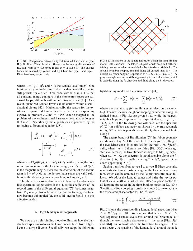
We now use a tight-binding model to illustrate how the Lan-dau level spectra evolve as the Dirac cone is titled from a type-I cone to a type-II cone. Specifically, we adopt the following
A1
B1 B2
A2
kx
ky
k1
k2
ta
tb
tc
td
FIG. S2. Illustration of the square lattice, on which the tight-bindingmodel (C4) is defined. The lattice is bipartite with each unit cell con-taining two inequivalent atoms labeled by A (red) and B (black). Thesecond neighbor hopping integral along all dashed lines is t1. Thenearest-neighbor hopping is specified as ta = tb = tc = −t, td = t. Thegray rectangle marks the ribbon geometry in our calculation, whichis periodic along the k2 direction and finite along the k1 direction.
tight-binding model on the square lattice [24],
H = −∑〈i j〉
ti jb†
jai + t1∑〈i j〉
(a†jai + b†jbi
), (C4)
where the operator ai (bi) annihilates an electron on site Ai(Bi). The next-nearest-neighbor hopping parameters along thedashed bonds in Fig. S2 are given by t1, while the nearest-neighbor hopping amplitude ti j are specified as ta = tb = tc =
−t, td = t. In the following, we will calculate the spectrumof (C4) in a ribbon geometry, as shown by the gray rectanglein Fig. S2, which is periodic along the k2 direction and finitealong k1.
The energy bands of Hamiltonian (C4) in ribbon geometryare shown in Fig. 5 of the main text. The degree of tilting ofthe two Dirac cones is controlled by the ratio t1/t. Specifi-cally, when t1/t = 0 there is no tilting [Fig. 5(a)]; when t1/tstarts to increase, the two Dirac cones begin to tilt [Fig. 5(b)];when t1/t = 1/2 the spectrum is nondispersive along the k2direction [Fig. 5(c)]; finally, when t1/t > 1/2, type-II Diraccones appear [Fig. 5(d)].
Such a transition from a type-I to a type-II Dirac cone alsomanifests itself in a drastic change in the Landau level struc-ture, which can be obtained by the Peierls substitution as fol-lows. We adopt the Landau gauge and write the vector po-tential as A = (0, Bx), which will attach a phase factor forall hopping processes in the tight-binding model in Eq. (C4).Specifically, for a hopping from lattice point (xi, yi) to (x f , y f ),the associated phase factor will be eiθ, with
θ =e~
∫C
A·dr =(x f + xi)(y f − yi)
2`2B
. (C5)
Fig. 5 shows the corresponding Landau level spectrum whenλ ≡ Ba2/φ0 = 0.01. We can see that when t1/t < 0.5,well separated Landau levels exist around the Dirac node, al-though the level spacing decreases as t1 increases [Figs. 5(a)and 5(b)]. In contrast, when the transition to a type-II Diraccone occurs, the spacing of the Landau level around the node

13
FIG. S3. (a) Bulk energy spectrum of model (C7) as a function ok k2 with k1 = 0. (b) Energy spectrum of Hamiltonian (C7) in a ribbongeometry with the edges along the k2 direction. (c) Landau level spectrum of Hamiltonian (C7) with λ ≡ Ba2/φ0 = 0.05. We note that alldispersive curves in the Landau level structure arise from states localized at the edge of the ribbon.
becomes extremely small; the Landau levels with finite sepa-ration are due to the contributions from other parts of the bandstructure [Figs. 5(c) and 5(d)].
The change in the Landau level structure stems from achange in the Fermi surface topology. In fact, it is generallyexpected that a large Fermi surface area is associated withdense Landau levels. One simple example is type-I Diraccones with different Fermi velocities: for a given energy,the one with a smaller (larger) Fermi velocity has a larger(smaller) Fermi surface area, which is also associated witha small (large) Landau level spacing. One can also gain anintuitive understanding of this from a semiclassical point ofview [42, 43]. We first note that the Landau levels will oc-cur whenever the semiclassical orbits of electrons in k-spaceencloses some critical areas specified by the following condi-tion [42],
B2·
∮Cm
kc × dkc = 2π(m +
12−
ΓCm
2π
)eB~, (C6)
where Cm is the mth semiclassical orbit of the electron, andΓCm is the Berry phase of this energy contour. We thus seethat an additional Landau level will be formed whenever thearea of the k-space semiclassical orbit increases by 2πeB/~.In particular, note that this increment is independent of theLandau level index m. We can now explain why a large Fermisurface is usually associated with dense Landau levels: a largeFermi surface indicates a semiclassical orbit with a large cir-cumference, and thus a small change in the semiclassical orbitsize |∆kc| is sufficient to reach the next critical area. As a re-sult, as long as the Fermi velocity is not extremely large, weshould expect only a small change in the Landau level en-ergy. Therefore, a large Fermi surface area is usually associ-ated with dense Landau levels.
3. Relation to the (111) surface states
We now discuss the Landau level structure for the (111)surface states of the antiperovskite Ca3PbO. As shown inFig. 4(b) of the main text, the characteristics of the spectrumon the (111) surface is that two type-I Dirac nodes are locatedat the Γ point and that their energies are higher than the type-II
Dirac nodes away from the Γ point. To describe this surfacespectrum we consider the following effective model
Hk/t =
εa(k) γk Tk 0γ†k εb(k) 0 TkTk 0 εc(k) γk0 Tk γ†k εd(k)
, (C7)
where t is an overall energy multiplier and
εα(k) = Wα[cos(akx) + cos(aky)] + Mα, α = a, b, c, d. (C8)
Here, a is the distance |A1B1| in Fig. S2. Moreover, we haveγk = sin(akx) − i sin(aky), and Tk = v2 sin(akx) sin(aky).For the numerical evaluations we choose the parametersas (Wa,Ma) = (2.58,−0.50), (Wb,Mb) = (−0.42, 5.50),(Wc,Mc) = (1.16, 0), (Wd,Md) = (3.16,−4.00), and v2 =
0.25, respectively. The energy spectrum of this model atk1 = 0 is shown in Fig. S3(a), which captures the Dirac fea-tures of the (111) surface state [cf. Fig. 4(b) in the main text].We note that this effective model possesses a C3 rotation sym-metry, instead of the C4 rotation symmetry in the actual (111)surface of the antiperovskites; hence, there are four type-IIDirac nodes, instead of six.
In order to calculate the Landau level spectrum of thismodel, we assume that it is defined on the square latticeshown in Fig. S2, where each site now hosts four orbitals(Ak, Bk,Ck,Dk), which constitutes the basis of the Hamilto-nian Hk, Eq. (C7). For convenience, we also make a coordi-nate transformation, namely k1 = kx +ky, and k2 = kx−ky. Wethen keep the system periodic along the k2 direction, whilefinite along the k1 direction. In particular, we only retainthe lattice points marked by the gray rectangle in Fig. S2.The energy spectrum of such a ribbon geometry is shown inFig. S3(b). The Landau level spectrum of (C7) for φ/φ0 =
0.05 is shown in Fig. S3(c). The type-I and type-II Diracnodes exhibit distinguishable physical features. Near the type-I Dirac node at E/t ∼ 4.5, Landau levels are well separatedsince only a single Fermi surface appears near the node. Nearthe type-II Dirac nodes and the second type-I Dirac node atE/t ∼ 1.5, on the other hand, the spacing of the Landau lev-els is close to zero due to the complexity of the Fermi surfacestructures.
14
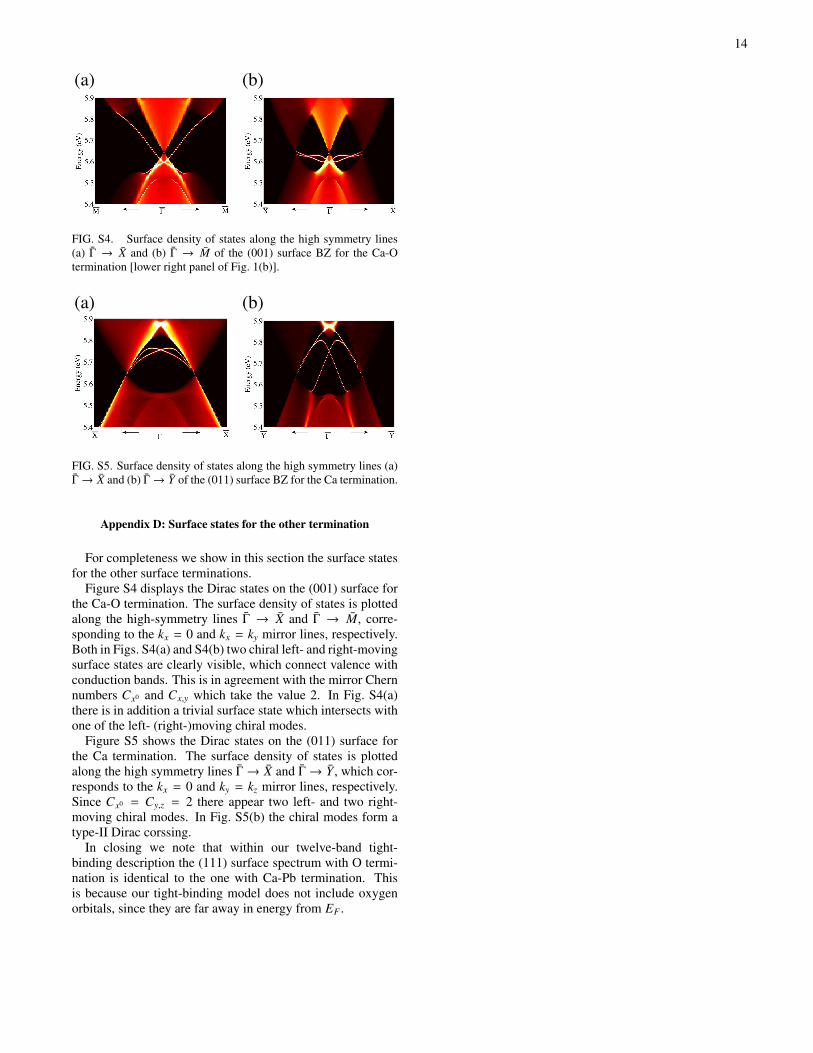
(a) (b)
FIG. S4. Surface density of states along the high symmetry lines(a) Γ → X and (b) Γ → M of the (001) surface BZ for the Ca-Otermination [lower right panel of Fig. 1(b)].
(a) (b)
FIG. S5. Surface density of states along the high symmetry lines (a)Γ→ X and (b) Γ→ Y of the (011) surface BZ for the Ca termination.
Appendix D: Surface states for the other termination
For completeness we show in this section the surface statesfor the other surface terminations.
Figure S4 displays the Dirac states on the (001) surface forthe Ca-O termination. The surface density of states is plottedalong the high-symmetry lines Γ → X and Γ → M, corre-sponding to the kx = 0 and kx = ky mirror lines, respectively.Both in Figs. S4(a) and S4(b) two chiral left- and right-movingsurface states are clearly visible, which connect valence withconduction bands. This is in agreement with the mirror Chernnumbers Cx0 and Cx,y which take the value 2. In Fig. S4(a)there is in addition a trivial surface state which intersects withone of the left- (right-)moving chiral modes.
Figure S5 shows the Dirac states on the (011) surface forthe Ca termination. The surface density of states is plottedalong the high symmetry lines Γ→ X and Γ→ Y , which cor-responds to the kx = 0 and ky = kz mirror lines, respectively.Since Cx0 = Cy,z = 2 there appear two left- and two right-moving chiral modes. In Fig. S5(b) the chiral modes form atype-II Dirac corssing.
In closing we note that within our twelve-band tight-binding description the (111) surface spectrum with O termi-nation is identical to the one with Ca-Pb termination. Thisis because our tight-binding model does not include oxygenorbitals, since they are far away in energy from EF .