TU0456 Tutorial SmartFusion2 SoC FPGA PCIe Control Plane ...
74
TU0456 Tutorial SmartFusion2 SoC FPGA PCIe Control Plane - Libero SoC v11.8 SP1
Transcript of TU0456 Tutorial SmartFusion2 SoC FPGA PCIe Control Plane ...

TU0456Tutorial
SmartFusion2 SoC FPGA PCIe Control Plane -Libero SoC v11.8 SP1

50200456. 9.0 9/17
Microsemi Corporate HeadquartersOne Enterprise, Aliso Viejo,CA 92656 USAWithin the USA: +1 (800) 713-4113 Outside the USA: +1 (949) 380-6100Fax: +1 (949) 215-4996Email: [email protected]
© 2017 Microsemi Corporation. All rights reserved. Microsemi and the Microsemi logo are trademarks of Microsemi Corporation. All other trademarks and service marks are the property of their respective owners.
Microsemi makes no warranty, representation, or guarantee regarding the information contained herein or the suitability of its products and services for any particular purpose, nor does Microsemi assume any liability whatsoever arising out of the application or use of any product or circuit. The products sold hereunder and any other products sold by Microsemi have been subject to limited testing and should not be used in conjunction with mission-critical equipment or applications. Any performance specifications are believed to be reliable but are not verified, and Buyer must conduct and complete all performance and other testing of the products, alone and together with, or installed in, any end-products. Buyer shall not rely on any data and performance specifications or parameters provided by Microsemi. It is the Buyer's responsibility to independently determine suitability of any products and to test and verify the same. The information provided by Microsemi hereunder is provided “as is, where is” and with all faults, and the entire risk associated with such information is entirely with the Buyer. Microsemi does not grant, explicitly or implicitly, to any party any patent rights, licenses, or any other IP rights, whether with regard to such information itself or anything described by such information. Information provided in this document is proprietary to Microsemi, and Microsemi reserves the right to make any changes to the information in this document or to any products and services at any time without notice.
About Microsemi
Microsemi Corporation (Nasdaq: MSCC) offers a comprehensive portfolio of semiconductor and system solutions for aerospace & defense, communications, data center and industrial markets. Products include high-performance and radiation-hardened analog mixed-signal integrated circuits, FPGAs, SoCs and ASICs; power management products; timing and synchronization devices and precise time solutions, setting the world's standard for time; voice processing devices; RF solutions; discrete components; enterprise storage and communication solutions, security technologies and scalable anti-tamper products; Ethernet solutions; Power-over-Ethernet ICs and midspans; as well as custom design capabilities and services. Microsemi is headquartered in Aliso Viejo, California, and has approximately 4,800 employees globally. Learn more at www.microsemi.com.

TU0456 Tutorial Revision 9.0 iii
Contents
1 Revision History . . . . . . . . . . . . . . . . . . . . . . . . . . . . . . . . . . . . . . . . . . . . . . . . . . . . . 11.1 Revision 9.0 . . . . . . . . . . . . . . . . . . . . . . . . . . . . . . . . . . . . . . . . . . . . . . . . . . . . . . . . . . . . . . . . . . . . . . . 1
1.2 Revision 8.0 . . . . . . . . . . . . . . . . . . . . . . . . . . . . . . . . . . . . . . . . . . . . . . . . . . . . . . . . . . . . . . . . . . . . . . . 1
1.3 Revision 7.0 . . . . . . . . . . . . . . . . . . . . . . . . . . . . . . . . . . . . . . . . . . . . . . . . . . . . . . . . . . . . . . . . . . . . . . . 1
1.4 Revision 6.0 . . . . . . . . . . . . . . . . . . . . . . . . . . . . . . . . . . . . . . . . . . . . . . . . . . . . . . . . . . . . . . . . . . . . . . . 1
1.5 Revision 5.0 . . . . . . . . . . . . . . . . . . . . . . . . . . . . . . . . . . . . . . . . . . . . . . . . . . . . . . . . . . . . . . . . . . . . . . . 1
1.6 Revision 4.0 . . . . . . . . . . . . . . . . . . . . . . . . . . . . . . . . . . . . . . . . . . . . . . . . . . . . . . . . . . . . . . . . . . . . . . . 1
1.7 Revision 3.0 . . . . . . . . . . . . . . . . . . . . . . . . . . . . . . . . . . . . . . . . . . . . . . . . . . . . . . . . . . . . . . . . . . . . . . . 1
1.8 Revision 2.0 . . . . . . . . . . . . . . . . . . . . . . . . . . . . . . . . . . . . . . . . . . . . . . . . . . . . . . . . . . . . . . . . . . . . . . . 1
1.9 Revision 1.0 . . . . . . . . . . . . . . . . . . . . . . . . . . . . . . . . . . . . . . . . . . . . . . . . . . . . . . . . . . . . . . . . . . . . . . . 1
1.10 Revision 0 . . . . . . . . . . . . . . . . . . . . . . . . . . . . . . . . . . . . . . . . . . . . . . . . . . . . . . . . . . . . . . . . . . . . . . . . 1
2 SmartFusion2 SoC FPGA - PCIe Control Plane Tutorial . . . . . . . . . . . . . . . . . . . . . 22.1 Design Requirements . . . . . . . . . . . . . . . . . . . . . . . . . . . . . . . . . . . . . . . . . . . . . . . . . . . . . . . . . . . . . . . 3
2.2 Design Files . . . . . . . . . . . . . . . . . . . . . . . . . . . . . . . . . . . . . . . . . . . . . . . . . . . . . . . . . . . . . . . . . . . . . . . 3
2.3 Design Description . . . . . . . . . . . . . . . . . . . . . . . . . . . . . . . . . . . . . . . . . . . . . . . . . . . . . . . . . . . . . . . . . . 4
2.4 Building the Design . . . . . . . . . . . . . . . . . . . . . . . . . . . . . . . . . . . . . . . . . . . . . . . . . . . . . . . . . . . . . . . . . 5
2.5 Step 1: Creating a Libero SoC Project . . . . . . . . . . . . . . . . . . . . . . . . . . . . . . . . . . . . . . . . . . . . . . . . . . . 52.5.1 Instantiating SERDESIF Component in PCIe_Demo SmartDesign . . . . . . . . . . . . . . . . . . . . . 162.5.2 Instantiating Debounce Logic in PCIe_Demo SmartDesign . . . . . . . . . . . . . . . . . . . . . . . . . . 192.5.3 Connecting Components in PCIe_Demo SmartDesign . . . . . . . . . . . . . . . . . . . . . . . . . . . . . . 202.5.4 Configuring and Generating Firmware . . . . . . . . . . . . . . . . . . . . . . . . . . . . . . . . . . . . . . . . . . 25
2.6 Step 2: Creating an eNVM Client . . . . . . . . . . . . . . . . . . . . . . . . . . . . . . . . . . . . . . . . . . . . . . . . . . . . . . 26
2.7 Step 3: Developing the Simulation Stimulus . . . . . . . . . . . . . . . . . . . . . . . . . . . . . . . . . . . . . . . . . . . . . 39
2.8 Step 4: Simulating the Design . . . . . . . . . . . . . . . . . . . . . . . . . . . . . . . . . . . . . . . . . . . . . . . . . . . . . . . . 42
2.9 Step 5: Generating the Program File . . . . . . . . . . . . . . . . . . . . . . . . . . . . . . . . . . . . . . . . . . . . . . . . . . . 46
2.10 Design Setup . . . . . . . . . . . . . . . . . . . . . . . . . . . . . . . . . . . . . . . . . . . . . . . . . . . . . . . . . . . . . . . . . . . . . 49
2.11 Running the Design . . . . . . . . . . . . . . . . . . . . . . . . . . . . . . . . . . . . . . . . . . . . . . . . . . . . . . . . . . . . . . . . 502.11.1 Running the Design on Windows . . . . . . . . . . . . . . . . . . . . . . . . . . . . . . . . . . . . . . . . . . . . . . 512.11.2 Running the Design on Linux . . . . . . . . . . . . . . . . . . . . . . . . . . . . . . . . . . . . . . . . . . . . . . . . . 59
2.12 Conclusion . . . . . . . . . . . . . . . . . . . . . . . . . . . . . . . . . . . . . . . . . . . . . . . . . . . . . . . . . . . . . . . . . . . . . . . 68

Figures
Figure 1 PCIe Control Plane Tutorial Top-Level Block Diagram . . . . . . . . . . . . . . . . . . . . . . . . . . . . . . . . . . . 2Figure 2 Design Files Top-Level Structure . . . . . . . . . . . . . . . . . . . . . . . . . . . . . . . . . . . . . . . . . . . . . . . . . . . 3Figure 3 PCIe Control Plane Block Diagram . . . . . . . . . . . . . . . . . . . . . . . . . . . . . . . . . . . . . . . . . . . . . . . . . . 4Figure 4 Libero SoC v 11.8 SP1 Project Manager . . . . . . . . . . . . . . . . . . . . . . . . . . . . . . . . . . . . . . . . . . . . . 5Figure 5 Device Selection Tab . . . . . . . . . . . . . . . . . . . . . . . . . . . . . . . . . . . . . . . . . . . . . . . . . . . . . . . . . . . . 6Figure 6 Device Settings Tab . . . . . . . . . . . . . . . . . . . . . . . . . . . . . . . . . . . . . . . . . . . . . . . . . . . . . . . . . . . . . 6Figure 7 Design Template Tab . . . . . . . . . . . . . . . . . . . . . . . . . . . . . . . . . . . . . . . . . . . . . . . . . . . . . . . . . . . . 7Figure 8 Add HDL Source Files Tab . . . . . . . . . . . . . . . . . . . . . . . . . . . . . . . . . . . . . . . . . . . . . . . . . . . . . . . . 7Figure 9 Add Constraints Tab . . . . . . . . . . . . . . . . . . . . . . . . . . . . . . . . . . . . . . . . . . . . . . . . . . . . . . . . . . . . . 8Figure 10 New Project Information . . . . . . . . . . . . . . . . . . . . . . . . . . . . . . . . . . . . . . . . . . . . . . . . . . . . . . . . . . 8Figure 11 System Builder Dialog Box . . . . . . . . . . . . . . . . . . . . . . . . . . . . . . . . . . . . . . . . . . . . . . . . . . . . . . . . 9Figure 12 SmartFusion2 System Builder Configurator . . . . . . . . . . . . . . . . . . . . . . . . . . . . . . . . . . . . . . . . . . . 9Figure 13 System Builder—Peripherals Page . . . . . . . . . . . . . . . . . . . . . . . . . . . . . . . . . . . . . . . . . . . . . . . . 10Figure 14 System Builder—Peripherals Page . . . . . . . . . . . . . . . . . . . . . . . . . . . . . . . . . . . . . . . . . . . . . . . . 11Figure 15 Configuring AMBA Master . . . . . . . . . . . . . . . . . . . . . . . . . . . . . . . . . . . . . . . . . . . . . . . . . . . . . . . 11Figure 16 System Builder—Peripherals Page . . . . . . . . . . . . . . . . . . . . . . . . . . . . . . . . . . . . . . . . . . . . . . . . 12Figure 17 GPIO Configuration . . . . . . . . . . . . . . . . . . . . . . . . . . . . . . . . . . . . . . . . . . . . . . . . . . . . . . . . . . . . 13Figure 18 System Builder—Clock Page . . . . . . . . . . . . . . . . . . . . . . . . . . . . . . . . . . . . . . . . . . . . . . . . . . . . . 14Figure 19 SmartFusion2 System Builder Generated System . . . . . . . . . . . . . . . . . . . . . . . . . . . . . . . . . . . . . 15Figure 20 IP Catalog . . . . . . . . . . . . . . . . . . . . . . . . . . . . . . . . . . . . . . . . . . . . . . . . . . . . . . . . . . . . . . . . . . . . 16Figure 21 SERDES Configurator . . . . . . . . . . . . . . . . . . . . . . . . . . . . . . . . . . . . . . . . . . . . . . . . . . . . . . . . . . 16Figure 22 PCIe Configuration for Protocol 1 . . . . . . . . . . . . . . . . . . . . . . . . . . . . . . . . . . . . . . . . . . . . . . . . . . 17Figure 23 PCIe Configuration Memory . . . . . . . . . . . . . . . . . . . . . . . . . . . . . . . . . . . . . . . . . . . . . . . . . . . . . . 18Figure 24 DEBOUNCE Component in Design Hierarchy Window . . . . . . . . . . . . . . . . . . . . . . . . . . . . . . . . . 19Figure 25 DEBOUNCE Component in Design Hierarchy . . . . . . . . . . . . . . . . . . . . . . . . . . . . . . . . . . . . . . . . 19Figure 26 Quick Connect Window . . . . . . . . . . . . . . . . . . . . . . . . . . . . . . . . . . . . . . . . . . . . . . . . . . . . . . . . . 20Figure 27 PCIe Demo Top in SmartDesign . . . . . . . . . . . . . . . . . . . . . . . . . . . . . . . . . . . . . . . . . . . . . . . . . . 21Figure 28 Edit Slices . . . . . . . . . . . . . . . . . . . . . . . . . . . . . . . . . . . . . . . . . . . . . . . . . . . . . . . . . . . . . . . . . . . . 22Figure 29 Edit Slices . . . . . . . . . . . . . . . . . . . . . . . . . . . . . . . . . . . . . . . . . . . . . . . . . . . . . . . . . . . . . . . . . . . . 23Figure 30 PCIe_Demo Top Design . . . . . . . . . . . . . . . . . . . . . . . . . . . . . . . . . . . . . . . . . . . . . . . . . . . . . . . . . 24Figure 31 Generate Component . . . . . . . . . . . . . . . . . . . . . . . . . . . . . . . . . . . . . . . . . . . . . . . . . . . . . . . . . . . 24Figure 32 Log Window . . . . . . . . . . . . . . . . . . . . . . . . . . . . . . . . . . . . . . . . . . . . . . . . . . . . . . . . . . . . . . . . . . 25Figure 33 Configuring Firmware . . . . . . . . . . . . . . . . . . . . . . . . . . . . . . . . . . . . . . . . . . . . . . . . . . . . . . . . . . . 25Figure 34 Export Firmware Dialog Box . . . . . . . . . . . . . . . . . . . . . . . . . . . . . . . . . . . . . . . . . . . . . . . . . . . . . . 25Figure 35 Log Window . . . . . . . . . . . . . . . . . . . . . . . . . . . . . . . . . . . . . . . . . . . . . . . . . . . . . . . . . . . . . . . . . . 25Figure 36 SoftConsole IDE Project Workspace . . . . . . . . . . . . . . . . . . . . . . . . . . . . . . . . . . . . . . . . . . . . . . . 26Figure 37 Creating New C Project . . . . . . . . . . . . . . . . . . . . . . . . . . . . . . . . . . . . . . . . . . . . . . . . . . . . . . . . . 27Figure 38 C Project Window . . . . . . . . . . . . . . . . . . . . . . . . . . . . . . . . . . . . . . . . . . . . . . . . . . . . . . . . . . . . . . 28Figure 39 C Project—Select Configuration . . . . . . . . . . . . . . . . . . . . . . . . . . . . . . . . . . . . . . . . . . . . . . . . . . . 28Figure 40 C Project—Cross GNU ARM Tool Chain . . . . . . . . . . . . . . . . . . . . . . . . . . . . . . . . . . . . . . . . . . . . 29Figure 41 Project Explorer—Import . . . . . . . . . . . . . . . . . . . . . . . . . . . . . . . . . . . . . . . . . . . . . . . . . . . . . . . . 29Figure 42 Import Window . . . . . . . . . . . . . . . . . . . . . . . . . . . . . . . . . . . . . . . . . . . . . . . . . . . . . . . . . . . . . . . . 30Figure 43 Import—File System . . . . . . . . . . . . . . . . . . . . . . . . . . . . . . . . . . . . . . . . . . . . . . . . . . . . . . . . . . . . 30Figure 44 Project Explorer—Source File . . . . . . . . . . . . . . . . . . . . . . . . . . . . . . . . . . . . . . . . . . . . . . . . . . . . 31Figure 45 Creating the main.c File . . . . . . . . . . . . . . . . . . . . . . . . . . . . . . . . . . . . . . . . . . . . . . . . . . . . . . . . . 31Figure 46 The main.c File . . . . . . . . . . . . . . . . . . . . . . . . . . . . . . . . . . . . . . . . . . . . . . . . . . . . . . . . . . . . . . . . 32Figure 47 Project Explorer window—Properties . . . . . . . . . . . . . . . . . . . . . . . . . . . . . . . . . . . . . . . . . . . . . . . 32Figure 48 Properties for PCIe_Demo_sb_MSS_CM3 . . . . . . . . . . . . . . . . . . . . . . . . . . . . . . . . . . . . . . . . . . 33Figure 49 Properties for PCIe_Demo_sb_MSS_CM3—General . . . . . . . . . . . . . . . . . . . . . . . . . . . . . . . . . . 34Figure 50 Properties for PCIe_Demo_sb_MSS_CM3—Miscellaneous . . . . . . . . . . . . . . . . . . . . . . . . . . . . . 35Figure 51 Project Window—Release Mode . . . . . . . . . . . . . . . . . . . . . . . . . . . . . . . . . . . . . . . . . . . . . . . . . . 35Figure 52 Project Explorer—Build Project . . . . . . . . . . . . . . . . . . . . . . . . . . . . . . . . . . . . . . . . . . . . . . . . . . . 36Figure 53 System Builder—Memory eNVM . . . . . . . . . . . . . . . . . . . . . . . . . . . . . . . . . . . . . . . . . . . . . . . . . . 36Figure 54 Add Data Storage Client . . . . . . . . . . . . . . . . . . . . . . . . . . . . . . . . . . . . . . . . . . . . . . . . . . . . . . . . . 37
TU0456 Tutorial Revision 9.0 iv

Figure 55 Browsing for .hex File . . . . . . . . . . . . . . . . . . . . . . . . . . . . . . . . . . . . . . . . . . . . . . . . . . . . . . . . . . . 37Figure 56 Add Data Storage Client . . . . . . . . . . . . . . . . . . . . . . . . . . . . . . . . . . . . . . . . . . . . . . . . . . . . . . . . . 38Figure 57 Modify Core—ENVM . . . . . . . . . . . . . . . . . . . . . . . . . . . . . . . . . . . . . . . . . . . . . . . . . . . . . . . . . . . 38Figure 58 SmartDesign Generated SERDESIF_0_PCIE_0_user.bfm File . . . . . . . . . . . . . . . . . . . . . . . . . . . 39Figure 59 Modified SERDES User BFM . . . . . . . . . . . . . . . . . . . . . . . . . . . . . . . . . . . . . . . . . . . . . . . . . . . . . 41Figure 60 HDL Testbench . . . . . . . . . . . . . . . . . . . . . . . . . . . . . . . . . . . . . . . . . . . . . . . . . . . . . . . . . . . . . . . . 42Figure 61 Create New HDL Testbench File . . . . . . . . . . . . . . . . . . . . . . . . . . . . . . . . . . . . . . . . . . . . . . . . . . 42Figure 62 Wave.do File under Simulation Folder . . . . . . . . . . . . . . . . . . . . . . . . . . . . . . . . . . . . . . . . . . . . . . 43Figure 63 Project Setting—Do File Simulation Runtime Setting . . . . . . . . . . . . . . . . . . . . . . . . . . . . . . . . . . . 43Figure 64 Project Setting—Waveform . . . . . . . . . . . . . . . . . . . . . . . . . . . . . . . . . . . . . . . . . . . . . . . . . . . . . . 44Figure 65 SERDES BFM Simulation . . . . . . . . . . . . . . . . . . . . . . . . . . . . . . . . . . . . . . . . . . . . . . . . . . . . . . . . 45Figure 66 Simulation Result with MSS GPIO Signals . . . . . . . . . . . . . . . . . . . . . . . . . . . . . . . . . . . . . . . . . . . 45Figure 67 Manage Constraints . . . . . . . . . . . . . . . . . . . . . . . . . . . . . . . . . . . . . . . . . . . . . . . . . . . . . . . . . . . . 46Figure 68 Derive Constraints . . . . . . . . . . . . . . . . . . . . . . . . . . . . . . . . . . . . . . . . . . . . . . . . . . . . . . . . . . . . . 46Figure 69 Associate SDC File . . . . . . . . . . . . . . . . . . . . . . . . . . . . . . . . . . . . . . . . . . . . . . . . . . . . . . . . . . . . . 46Figure 70 Edit with I/O Editor . . . . . . . . . . . . . . . . . . . . . . . . . . . . . . . . . . . . . . . . . . . . . . . . . . . . . . . . . . . . . 47Figure 71 I/O Editor . . . . . . . . . . . . . . . . . . . . . . . . . . . . . . . . . . . . . . . . . . . . . . . . . . . . . . . . . . . . . . . . . . . . . 48Figure 72 Generate Bitstream . . . . . . . . . . . . . . . . . . . . . . . . . . . . . . . . . . . . . . . . . . . . . . . . . . . . . . . . . . . . . 48Figure 73 Run PROGRAM Action . . . . . . . . . . . . . . . . . . . . . . . . . . . . . . . . . . . . . . . . . . . . . . . . . . . . . . . . . . 49Figure 74 SmartFusion2 Security Evaluation Kit Setup . . . . . . . . . . . . . . . . . . . . . . . . . . . . . . . . . . . . . . . . . 50Figure 75 Device Manager—PCIe Device Detection . . . . . . . . . . . . . . . . . . . . . . . . . . . . . . . . . . . . . . . . . . . 51Figure 76 Update Driver Software . . . . . . . . . . . . . . . . . . . . . . . . . . . . . . . . . . . . . . . . . . . . . . . . . . . . . . . . . 52Figure 77 Browse for Driver Software . . . . . . . . . . . . . . . . . . . . . . . . . . . . . . . . . . . . . . . . . . . . . . . . . . . . . . . 52Figure 78 Browse for Driver Software Continued . . . . . . . . . . . . . . . . . . . . . . . . . . . . . . . . . . . . . . . . . . . . . . 53Figure 79 Windows Security . . . . . . . . . . . . . . . . . . . . . . . . . . . . . . . . . . . . . . . . . . . . . . . . . . . . . . . . . . . . . . 53Figure 80 Successful Driver Installation . . . . . . . . . . . . . . . . . . . . . . . . . . . . . . . . . . . . . . . . . . . . . . . . . . . . . 53Figure 81 GUI Installation . . . . . . . . . . . . . . . . . . . . . . . . . . . . . . . . . . . . . . . . . . . . . . . . . . . . . . . . . . . . . . . . 54Figure 82 Successful GUI Installation . . . . . . . . . . . . . . . . . . . . . . . . . . . . . . . . . . . . . . . . . . . . . . . . . . . . . . . 54Figure 83 Device Manager—PCIe Device Detection . . . . . . . . . . . . . . . . . . . . . . . . . . . . . . . . . . . . . . . . . . . 55Figure 84 PCIe Demo GUI . . . . . . . . . . . . . . . . . . . . . . . . . . . . . . . . . . . . . . . . . . . . . . . . . . . . . . . . . . . . . . . 55Figure 85 Device Info . . . . . . . . . . . . . . . . . . . . . . . . . . . . . . . . . . . . . . . . . . . . . . . . . . . . . . . . . . . . . . . . . . . 56Figure 86 Demo Controls . . . . . . . . . . . . . . . . . . . . . . . . . . . . . . . . . . . . . . . . . . . . . . . . . . . . . . . . . . . . . . . . 56Figure 87 Demo Controls—Continued . . . . . . . . . . . . . . . . . . . . . . . . . . . . . . . . . . . . . . . . . . . . . . . . . . . . . . 57Figure 88 Configuration Space . . . . . . . . . . . . . . . . . . . . . . . . . . . . . . . . . . . . . . . . . . . . . . . . . . . . . . . . . . . . 57Figure 89 PCIe BAR1 Memory Access . . . . . . . . . . . . . . . . . . . . . . . . . . . . . . . . . . . . . . . . . . . . . . . . . . . . . . 58Figure 90 PCIe Device Detection . . . . . . . . . . . . . . . . . . . . . . . . . . . . . . . . . . . . . . . . . . . . . . . . . . . . . . . . . . 59Figure 91 Edit board.h File . . . . . . . . . . . . . . . . . . . . . . . . . . . . . . . . . . . . . . . . . . . . . . . . . . . . . . . . . . . . . . . 60Figure 92 PCIe Device Driver Installation . . . . . . . . . . . . . . . . . . . . . . . . . . . . . . . . . . . . . . . . . . . . . . . . . . . . 60Figure 93 Linux PCIe Application Utility . . . . . . . . . . . . . . . . . . . . . . . . . . . . . . . . . . . . . . . . . . . . . . . . . . . . . 61Figure 94 Linux Command—LED Control . . . . . . . . . . . . . . . . . . . . . . . . . . . . . . . . . . . . . . . . . . . . . . . . . . . 62Figure 95 Linux Command—SRAM Read/Write . . . . . . . . . . . . . . . . . . . . . . . . . . . . . . . . . . . . . . . . . . . . . . . 63Figure 96 Linux Command—DIP Switch . . . . . . . . . . . . . . . . . . . . . . . . . . . . . . . . . . . . . . . . . . . . . . . . . . . . 64Figure 97 Linux Command—PCIe Configuration Space Display . . . . . . . . . . . . . . . . . . . . . . . . . . . . . . . . . . 65Figure 98 Linux Command—PCIe Link Speed and Width . . . . . . . . . . . . . . . . . . . . . . . . . . . . . . . . . . . . . . . 66Figure 99 Linux Command—PCIe Link Speed and Width . . . . . . . . . . . . . . . . . . . . . . . . . . . . . . . . . . . . . . . 67Figure 100 Linux Command—PCIe Interrupt Control . . . . . . . . . . . . . . . . . . . . . . . . . . . . . . . . . . . . . . . . . . . . 68
TU0456 Tutorial Revision 9.0 v

TU0456 Tutorial Revision 9.0 vi
Tables
Table 1 Hardware and Software Requirements . . . . . . . . . . . . . . . . . . . . . . . . . . . . . . . . . . . . . . . . . . . . . . . 3Table 2 FIC_0_PINS . . . . . . . . . . . . . . . . . . . . . . . . . . . . . . . . . . . . . . . . . . . . . . . . . . . . . . . . . . . . . . . . . . 21Table 3 SDIF0_PINS . . . . . . . . . . . . . . . . . . . . . . . . . . . . . . . . . . . . . . . . . . . . . . . . . . . . . . . . . . . . . . . . . . 21Table 4 INIT_PINS . . . . . . . . . . . . . . . . . . . . . . . . . . . . . . . . . . . . . . . . . . . . . . . . . . . . . . . . . . . . . . . . . . . . 22Table 5 Port to Pin Mapping . . . . . . . . . . . . . . . . . . . . . . . . . . . . . . . . . . . . . . . . . . . . . . . . . . . . . . . . . . . . 47Table 6 SmartFusion2 FPGA Security Evaluation Kit Jumper Settings . . . . . . . . . . . . . . . . . . . . . . . . . . . . 49

Revision History
TU0456 Tutorial Revision 9.0 1
1 Revision History
The revision history describes the changes that were implemented in the document. The changes are listed by revision, starting with the most current publication.
1.1 Revision 9.0Updated the document for Libero v11.8 SP1 software release.
1.2 Revision 8.0Updated the broken design files link.
1.3 Revision 7.0Updated push button description from SW3 to SW4 in (SAR 78370).
1.4 Revision 6.0Updated the document for Libero v11.7 software release (SAR 76664).
1.5 Revision 5.0Updated the document for Libero v11.6 software release (SAR 73139).
1.6 Revision 4.0Updated the document for Libero v11.5 software release (SAR 64184).
1.7 Revision 3.0Updated the document for Libero v11.4 software release (SAR 59644).
1.8 Revision 2.0Updated the document for Libero v11.3 software release (SAR 56081).
1.9 Revision 1.0Updated the document for Libero v11.2 software release (SAR 52109) (SAR 52909) and (SAR 50779).
1.10 Revision 0Revision 0 was the first publication of this document.

SmartFusion2 SoC FPGA - PCIe Control Plane Tutorial
2 SmartFusion2 SoC FPGA - PCIe Control Plane Tutorial
SmartFusion®2 SoC FPGA devices integrate a fourth generation flash-based FPGA fabric and an ARM Cortex-M3 processor, along with high performance communication interfaces on a single chip. The SmartFusion2 high-speed serial interface (SERDESIF) provides a fully hardened PCIe endpoint implementation and is compliant with PCIe Base Specification Revision 2.0, 1.1 and 1.0. For more information, see the UG0447: IGLOO2 and SmartFusion2 High Speed Serial Interfaces User Guide.
The tutorial explains the SmartFusion2 embedded PCI Express feature and how this can be used as a low bandwidth control plane interface using the SmartFusion2 Security Evaluation Kit. The tutorial provides a simple design to access the SmartFusion2 PCIe endpoint from a host PC. A GUI is provided for read and write access to the SmartFusion2 PCIe configuration space and memory space of BAR0 and BAR1. The tutorial also provides host PC device drivers for the SmartFusion2 PCIe endpoint. This tutorial can run on both windows and Red Hat Linux operating system.
The following figure shows the top-level block diagram for the PCIe control plane tutorial. The tutorial design uses a SmartFusion2 PCIe interface with a link width of ×1 to interface with a host PC PCIe Gen2 slot. The SmartFusion2 microcontroller subsystem (MSS) General Purpose I/Os (GPIOs) control the LEDs and switches on the SmartFusion2 Security Evaluation Kit through the PCIe interface. The host PC can also read memory and writes to the SmartFusion2 eSRAM through the GUI. The host PC can also be interrupted by using the push button on the SmartFusion2 Security Evaluation Kit.
Figure 1 • PCIe Control Plane Tutorial Top-Level Block Diagram
The design performs the following tasks:
• Displays the PCIe link enable or disable, negotiated link width, and the link speed.• Controls the status of LEDs on the SmartFusion2 Security Evaluation Kit according to the command
from the GUI.• Displays the position of DIP Switches on SmartFusion2 Security Evaluation Kit.• Enables read and write to eSRAM.• Interrupts the host PC, when the push button is pressed. The GUI displays the count value of the
number of interrupts sent from the SmartFusion2 Security Evaluation Kit.• Displays the SmartFusion2 PCIe Configuration Space.
TU0456 Tutorial Revision 9.0 2

SmartFusion2 SoC FPGA - PCIe Control Plane Tutorial
2.1 Design RequirementsThe following figure the hardware and software required to run the tutorial.
2.2 Design FilesThe design files for this tutorial can be downloaded from the Microsemi website:http://soc.microsemi.com/download/rsc/?f=m2s_tu0456_liberov11p8_sp1_df
The following figure shows the top-level structure of the design files. For further details, see the Readme.txt file.
Figure 2 • Design Files Top-Level Structure
Table 1 • Hardware and Software Requirements
Hardware Version
SmartFusion2 Security Evaluation Kit:– 12 V adapter (provided along with the kit)– FlashPro4 programmer (provided along with the kit)
Rev E or later
Host PC with an available PCIe 2.0 Gen1 or Gen2 compliant slot Operating system:Windows XP SP2: 64-bitWindows 7: 64-bitorRed Hat Linux Kernel Version: 2.6.18-308
Software
Libero® SoC Design Suite v11.8 SP1
SoftConsole v4.0
Host PC Drivers (provided along with the design files) –
GUI executable (provided along with the design files) –
TU0456 Tutorial Revision 9.0 3

SmartFusion2 SoC FPGA - PCIe Control Plane Tutorial
2.3 Design DescriptionThis design implements the SmartFusion2 embedded PCI Express interface as a low bandwidth control plane interface. This design provides host PC drivers and a host PC interface over PCIe to control the SmartFusion2 device. The following figure shows a detailed block diagram of the design implementation. The PCIe endpoint device receives commands from the host PC through the GUI and does corresponding memory writes to the SmartFusion2 MSS address space. The MSS address space provides a GPIO block and eSRAM memory block, which is accessed through a fabric interface controller (FIC_0).
The SERDES_IF2_0 is configured for a PCIe 2.0, x1 link width with GEN2 speed. The PCIe interface to the fabric uses an AMBA High-speed Bus (AHB). The AHB master interface of SERDESIF is enabled and connected to the AHB slave interface of FIC_0 to access the MSS peripherals. The SmartFusion2 PCIe BAR0 and BAR1 are configured in 32-bit memory mapped memory mode.
The AXI master windows of the SERDESIF PCIe provide address translation for accessing one address space from another address space as the PCIe address is different from SmartFusion2 AHB bus matrix address space. The AXI master window 0 is enabled and configured to translate the BAR0 memory address space to the MSS GPIO address space to control the MSS GPIOs. The AXI master window 1 is enabled and configured to translate the BAR1 memory address space to the eSRAM address space to perform read and writes from PCIe.
MSS GPIO block is enabled and configured as below:
• GPIO_0 to GPIO_7 as outputs and connected to LEDs• GPIO_8 to GPIO_11 as inputs and connected to DIP switches
The PCIe interrupt line is connected to the SW4 push button on the SmartFusion2 Security Evaluation Kit. The FPGA clocks are configured to run the FPGA fabric and MSS at 90 MHz.
Figure 3 • PCIe Control Plane Block Diagram
TU0456 Tutorial Revision 9.0 4

SmartFusion2 SoC FPGA - PCIe Control Plane Tutorial
2.4 Building the DesignThis section provides a complete design flow starting from a new project to a working design on the SmartFusion2 Security Evaluation Kit. This process includes usage of the tools in the Libero SoC design suite to program the SmartFusion2 device.
Building the design involves the following steps:
• Step 1: Creating a Libero SoC Project• Step 2: Creating an eNVM Client• Step 3: Developing the Simulation Stimulus• Step 4: Simulating the Design• Step 5: Generating the Program File
2.5 Step 1: Creating a Libero SoC ProjectThe following steps describe how to create a Libero SoC project:
1. Click Start > Programs > Microsemi Libero SoC v11.8 SP1 > Libero SoC v11.8 SP1, or click desktop shortcut. The Libero SoC v11.8 SP1 Project Manager is displayed, as shown in the following figure.
Figure 4 • Libero SoC v 11.8 SP1 Project Manager
2. Create a new project using one of the following options:• Select New on the Start Page tab as highlighted in the preceding figure.• Click Project > New Project from the Libero SoC menu.
3. Enter the following information in the New Project-Project Details tab, as shown in the following figure.• Project Name: PCIE_Demo• Project Location: Select an appropriate location (for example, D:/Microsemi_proj)• Preferred HDL Type: Verilog or VHDL
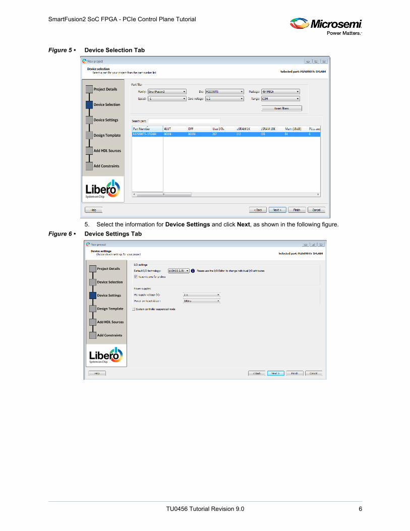
4. Select the information for Device Selection and click Next, as shown in the following figure.• Family: SmartFusion2• Die: M2S090TS• Package: 484 FBGA• Speed: -1• Core voltage: 1.2• Range: COM
TU0456 Tutorial Revision 9.0 5
SmartFusion2 SoC FPGA - PCIe Control Plane Tutorial
Figure 5 • Device Selection Tab
5. Select the information for Device Settings and click Next, as shown in the following figure.
Figure 6 • Device Settings Tab
TU0456 Tutorial Revision 9.0 6

SmartFusion2 SoC FPGA - PCIe Control Plane Tutorial
6. Design Template tab is displayed, as shown in the following figure. Select Create a System Builder based design under Design Templates and Creators and click Next.
Figure 7 • Design Template Tab
7. Add HDL Sources tab is displayed, as shown in the following figure. Verilog/VHDL Source Files can be added here.
Figure 8 • Add HDL Source Files Tab
TU0456 Tutorial Revision 9.0 7

SmartFusion2 SoC FPGA - PCIe Control Plane Tutorial
8. Add Constraints tab is displayed, as shown in the following figure. Constraints file can be added using Import option.
Figure 9 • Add Constraints Tab
9. Click Finish. This displays the New project information window. Select Use Enhanced Constraint Flow to use the new constraint flow as part of Libero v11.8 SP1 SoC, as shown in the following figure.
Figure 10 • New Project Information
TU0456 Tutorial Revision 9.0 8

SmartFusion2 SoC FPGA - PCIe Control Plane Tutorial
10. Enter PCIe_Demo as the name of the system in the System Builder dialog box, as shown in the following figure.
Figure 11 • System Builder Dialog Box
11. Click OK. The System Builder dialog box is displayed with the Device Features page open by default.
12. Enter the following information in the System Builder – Device Features page, as shown in the following figure:• Memory: Clear all except MSS On-chip Flash Memory (eNVM)• High-speed serial interfaces: Check SERDESIF_0• Microcontroller Options: Clear All
Figure 12 • SmartFusion2 System Builder Configurator
TU0456 Tutorial Revision 9.0 9

SmartFusion2 SoC FPGA - PCIe Control Plane Tutorial
13. Click Next. The System Builder – Memories page is displayed.14. Click Next. The System Builder – Peripherals page is displayed. Drag the Fabric AMBA Master
to MSS_FIC_0 – Fabric Master Subsystem, as shown in the following figure. It enables the MSS FIC_0 slave interface.
Figure 13 • System Builder—Peripherals Page
TU0456 Tutorial Revision 9.0 10

SmartFusion2 SoC FPGA - PCIe Control Plane Tutorial
15. Disable the MSS Peripherals except MSS_GPIO. The System Builder – Peripherals page is displayed. Configure MSS_FIC_0 – Fabric Master Subsystem for AHB-Lite by clicking AMBA_MASTER_0 configurator highlighted in the following figure. This displays a drop-down list, as shown in Figure 15, page 11.
Figure 14 • System Builder—Peripherals Page
16. Select AHBLite from the drop-down list, as shown in the following figure.
Figure 15 • Configuring AMBA Master
TU0456 Tutorial Revision 9.0 11

SmartFusion2 SoC FPGA - PCIe Control Plane Tutorial
17. Configure MSS_GPIO by clicking MSS_GPIO Configure, as shown in the following figure.
Figure 16 • System Builder—Peripherals Page
18. Double-click MSS_GPIO configuration, as shown in the following figure and configure:• GPIO_0 to GPIO_7 as outputs and their connectivity to FABRIC_A to connect with LEDs.• GPIO_8 to GPIO_11 as inputs and their connectivity to FABRIC_A, to connect with DIP
switches.This design requires configuring GPIO_0 to GPIO_7 to drive LED_1 to LED_8 on the SmartFusion2 Security Evaluation Kit, and GPIO_8 to GPIO_11 to connect DIP1 to DIP4. These signals are routed through the fabric to the I/O pins.
TU0456 Tutorial Revision 9.0 12

SmartFusion2 SoC FPGA - PCIe Control Plane Tutorial
The following figure shows the MSS GPIO Configurator.
Figure 17 • GPIO Configuration
19. Click OK on MSS GPIO Configurator.
TU0456 Tutorial Revision 9.0 13

SmartFusion2 SoC FPGA - PCIe Control Plane Tutorial
20. Click Next. The System Builder – Clock page is displayed, as shown in the following figure. Change the configuration of System Clock from 100 MHz to 50 MHz. The dedicated input pad is connected to on board 50 MHz oscillator. The M3_CLK is configured to 90 MHz by default.
Figure 18 • System Builder—Clock Page
21. Click Next. The System Builder - Microcontroller page is displayed. Leave all the default selections.
22. Click Next. The System Builder - SECDED page is displayed. Do not change the default selections.
23. Click Next. The System Builder - Security page is displayed. Do not change the default selections.24. Click Next. The System Builder - Interrupts page is displayed. Do not change the default
selections.25. Click Next. The System Builder - Memory Map page is displayed. Do not change the default
selections.26. Click Finish. The System Builder generates the system based on the selected options.
TU0456 Tutorial Revision 9.0 14

SmartFusion2 SoC FPGA - PCIe Control Plane Tutorial
The System Builder block is created and added to Libero SoC project automatically, as shown in the following figure.
Figure 19 • SmartFusion2 System Builder Generated System
The two soft cores (CoreResetP and CoreConfigP) are automatically instantiated and connected by the System Builder. The block connections can be seen by opening the System Builder component in the SmartDesign canvas.
Note: CoreResetP and CoreConfigP are responsible for the reset and configuration of ASIC peripherals. In this particular design, they are used to reset and configure the SERDESIF module. These modules are included in the System Builder generated component when an ASIC peripheral is selected.
TU0456 Tutorial Revision 9.0 15

SmartFusion2 SoC FPGA - PCIe Control Plane Tutorial
2.5.1 Instantiating SERDESIF Component in PCIe_Demo SmartDesignThe Libero SoC Catalog provides IP cores that can be easily dragged-and-dropped into the SmartDesign Canvas workspace. Many of these IPs are free to use while several require a license agreement. The SERDESIF module that supports the PCIe embedded interface is included in the catalog. To instantiate the SERDESIF component in the PCIe_Demo SmartDesign, expand the Peripherals category in the Libero SoC Catalog.
Figure 20 • IP Catalog
1. Drag the High Speed Serial Interface2 onto the PCIe_Demo SmartDesign canvas. If the component appears shadowed in the Vault, right-click the name and select Download.
2. Double-click the SERDES_IF2_0 component in the SmartDesign canvas to open the SERDES configurator. Configure the SERDES with the following settings, as shown in the following figure:• Select SERDESIF_0 • Simulation Level: BFM PCIe• Protocol1: Number of Lanes: x1• Protocol1: Type: PCIe• CLK_BASE Frequency (MHz): 90 • Lane Configuration: Speed: 5.0 Gbps(Gen2)• Reference Clock Source: REFCLK0 (Differential)
Figure 21 • SERDES Configurator
TU0456 Tutorial Revision 9.0 16

SmartFusion2 SoC FPGA - PCIe Control Plane Tutorial
3. Click Configure PCIe in Protocol1, as shown in Figure 21, page 16. The following settings are made in the Configuration tab, as shown in the following figure.– Fabric Interface (AXI/AHBLite)
• Bus: select as AHBLite from the drop-down list– Base Address Registers
• BAR 0 Width: 32-bit, Size: 1 MB (to access MSS Peripheral address space)• BAR 1 Width: 32-bit, Size: 64 KB (to access eSRAM memory)– Identification Registers
• Device ID: 0x11AA (MicroSemi ID)• Subsystem Vendor ID: 0x11AA (MicroSemi ID)
Figure 22 • PCIe Configuration for Protocol 1
TU0456 Tutorial Revision 9.0 17

SmartFusion2 SoC FPGA - PCIe Control Plane Tutorial
4. Click the Master Interface tab to configure the PCIe master windows. The PCIe AXI master windows are used to translate the PCIe address domain to the local device address domain. In this design the PCIe AXI master windows are used to translate the address of BAR0 and BAR1 to CoreGPIO address and COREAHBLSRAM address. Make settings, as shown in the following figure.– Select Window 0 and configure following settings:
• Size: Select as 1 MB from the drop-down list• PCIe BAR: Select as Bar0 from the drop-down list• Local Address: Enter values as 0x40000 to translate the BAR0 address space to CoreGPIO
address (0x4000_0000)– Select Window 1 and configure following settings:
• Size: Select as 64 KB from the drop-down list• PCIe BAR: Select as Bar1 from the drop-down list• Local Address: Enter values as 0x20000 to translate the BAR1 address space to
COREAHBLSRAM address (0x2000_0000)For more information on PCIe address translation, refer to the Address Translation on the AXI Master Interface section of the UG0447: IGLOO2 and SmartFusion2 High Speed Serial Interfaces User Guide.
Figure 23 • PCIe Configuration Memory
5. Click OK to close PCIe Configuration window.6. Click OK to save and close the High Speed Serial Interface Configurator.
TU0456 Tutorial Revision 9.0 18

SmartFusion2 SoC FPGA - PCIe Control Plane Tutorial
2.5.2 Instantiating Debounce Logic in PCIe_Demo SmartDesign1. The design provides a push button on the SmartFusion2 Security Evaluation Kit to send an interrupt
to the host PC. This push button generates switch bounce that causes multiple interrupts to PCIe. Debounce logic is required to avoid the switch bounce.
2. To add the debounce logic to the PCIe design, click File > Import > HDL Source files.3. Browse to the Debounce.v or Debounce.vhd file location in the design files folder:
M2S90_PCIE_Control_DEMO_DF/Source Files. The following figure shows the DEBOUNCE component in the Design Hierarchy window.
Figure 24 • DEBOUNCE Component in Design Hierarchy Window
4. Click the PCIe_Demo tab and drag the DEBOUNCE component from the Design Hierarchy into the PCIe_Demo SmartDesign canvas, as shown in the following figure. A SmartDesign symbol for the Verilog HDL file is automatically generated.
Figure 25 • DEBOUNCE Component in Design Hierarchy
TU0456 Tutorial Revision 9.0 19

SmartFusion2 SoC FPGA - PCIe Control Plane Tutorial
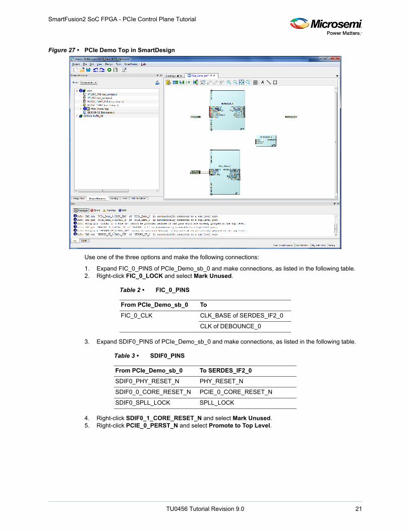
The PCIe_Demo is displayed, as shown in Figure 27, page 21. Connect the pins of all the blocks as described in the following section.
2.5.3 Connecting Components in PCIe_Demo SmartDesignThere are three methods for connecting components in PCIe_Demo SmartDesign.
The first method is by using the Connection Mode option. To use this method, change the SmartDesign to connection mode by clicking Connection Mode on the SmartDesign window, as shown in Figure 27, page 21. The cursor changes from the normal arrow shape to the connection mode icon shape. To make a connection in this mode, click on the first pin and drag-drop to the second pin that you want to connect.
The second method is by selecting the pins to be connected together and selecting Connect from the context menu. To select multiple pins to be connected together, press down the CTRL key while selecting the pins. Right-click the input source signal and select Connect to connect all the signals together. Similarly, select the input source signal, right-click it, and select Disconnect to disconnect the signals already connected.
The third method is by using the Quick Connect option. To use this method, change the SmartDesign to quick connect mode by clicking Quick Connect mode on the SmartDesign window, as shown in the following figure. Quick Connect window opens. Find the Instance Pin that needs to be connected and click to select it. In Pins to Connect, find the pin that needs to be connected, right-click and choose Connect, as shown in the following figure.
Figure 26 • Quick Connect Window
TU0456 Tutorial Revision 9.0 20
SmartFusion2 SoC FPGA - PCIe Control Plane Tutorial
Figure 27 • PCIe Demo Top in SmartDesign
Use one of the three options and make the following connections:
1. Expand FIC_0_PINS of PCIe_Demo_sb_0 and make connections, as listed in the following table.2. Right-click FIC_0_LOCK and select Mark Unused.
3. Expand SDIF0_PINS of PCIe_Demo_sb_0 and make connections, as listed in the following table.
4. Right-click SDIF0_1_CORE_RESET_N and select Mark Unused.5. Right-click PCIE_0_PERST_N and select Promote to Top Level.
Table 2 • FIC_0_PINS
From PCIe_Demo_sb_0 To
FIC_0_CLK CLK_BASE of SERDES_IF2_0
CLK of DEBOUNCE_0
Table 3 • SDIF0_PINS
From PCIe_Demo_sb_0 To SERDES_IF2_0
SDIF0_PHY_RESET_N PHY_RESET_N
SDIF0_0_CORE_RESET_N PCIE_0_CORE_RESET_N
SDIF0_SPLL_LOCK SPLL_LOCK
TU0456 Tutorial Revision 9.0 21

SmartFusion2 SoC FPGA - PCIe Control Plane Tutorial
6. Expand INIT_PINS of PCIe_Demo_sb_0 and make connections, as listed in the following table.
7. Right-click INIT_DONE and select Mark Unused.8. Connect MSS_READY of PCIe_Demo_sb_0 and RESET_N of DEBOUNCE_0.9. Right-click FAB_RESET_N of PCIe_Demo_sb_0 and select Tie High.10. Right-click GPIO_FABRIC of PCIe_Demo_sb_0 and select Promote to Top Level.11. Right-click POWER_ON_RESET_N of PCIe_Demo_sb_0 and select Mark Unused.12. Right-click SDIF_READY of PCIe_Demo_sb_0 and select Mark Unused.13. Connect AMBA_MASTER_0 of PCIe_Demo_sb_0 and AHB_MASTER of SERDES_IF2_0.14. Expand FAB_CCC_PINS, right-click FAB_CCC_GL3 and select Mark Unused.15. Connect SDIF1_INIT_APB of PCIe_Demo_sb_0 and APB_SLAVE of SERDES_IF2_0.16. Right-click the SWITCH of DEBOUNCE_0 and select Promote to Top Level.17. Select the following ports of SERDES_IF2_0 by pressing down the CTRL key, right-click, and select
Mark Unused.• PCIE_SYSTEM_INT • PLL_LOCK_INT• PLL_LOCKLOST_INT• PCIE_EV_1US• REFCLK0_OUT• PCIE_0_LTSSM[5:0]• PCIE_0_L2P2_ACTIVE• PCIE_0_RESET_PHASE
The PCIe supports four interrupts. This design uses only one interrupt out of four by connecting the unused interrupts to logic 0. To connect unused interrupt pins to logic 0 split the interrupt pins to two groups. Right-click the PCIE_INTERRUPT[3:0] of SERDES_IF2_0 and select Edit Slices to split. The Edit Slices window is displayed, as shown in the following figure.
Figure 28 • Edit Slices
Table 4 • INIT_PINS
From PCIe_Demo_sb_0 To SERDES_IF2_0
INIT_APB_S_PCLK APB_S_PCLK
INIT_APB_S_PRESET_N APB_S_PRESET_N
TU0456 Tutorial Revision 9.0 22

SmartFusion2 SoC FPGA - PCIe Control Plane Tutorial
18. Click the + sign and create a slice with the Left index 0 and the Right index 0. Click + again to create a second slice with Left index 3 and Right index 1, as shown in the following figure.
Figure 29 • Edit Slices
19. Expand PCIE_INTERRUPT[3:0], right-click the PCIE_INTERRUPT[3:1], and select Tie low.20. Connect INTERRUPT of DEBOUNCE_0 to the PCIE_INTERRUPT[0] of SERDES_IF2_0.
TU0456 Tutorial Revision 9.0 23

SmartFusion2 SoC FPGA - PCIe Control Plane Tutorial
21. Click Auto arrange instances to arrange the instances and click File > Save. The PCIe_Demo is displayed, as shown in the following figure.
Figure 30 • PCIe_Demo Top Design
22. Click the PCIe_Demo tab and click Generate Component, as shown in the following figure.
Figure 31 • Generate Component
TU0456 Tutorial Revision 9.0 24

SmartFusion2 SoC FPGA - PCIe Control Plane Tutorial
The message “PCIe_Demo” was successfully generated is displayed in the Libero SoC log window, if the design is generated without any error. On a successful component generation, the log window is displayed, as shown in the following figure.
Figure 32 • Log Window
2.5.4 Configuring and Generating FirmwareThe following steps describe how to configure and generate firmware.
1. Double-click Configure Firmware Cores under Handoff Design for Firmware Development in Design Flow and clear all drivers except CMSIS, as shown in the following figure.
Figure 33 • Configuring Firmware
2. Click Export Firmware. The Export Firmware dialog box is displayed, as shown in the following figure.
Figure 34 • Export Firmware Dialog Box
3. Browse the Location to export the firmware.4. Select the Create firmware project for check box.5. Select SoftConsole4.0 from the drop-down list.6. Click OK. The successful firmware generation window is displayed. 7. Click OK. The log window is displayed, as shown in the following figure.
Figure 35 • Log Window
TU0456 Tutorial Revision 9.0 25

SmartFusion2 SoC FPGA - PCIe Control Plane Tutorial
2.6 Step 2: Creating an eNVM Client The HDL and logical design portion of the design is now complete. The following sections describe the creation of the Cortex-M3 firmware used to initialize the MSS and SERDESIF.
The eNVM client has to be uploaded with the firmware application to initialize the SERDESIF through CoreConfigP. The Cortex-M3 processor executes the code in the eNVM after the SmartFusion2 device has been reset. In this design the eNVM client is created with the firmware application code to initialize the SERDESIF.
The following steps describe how to create an eNVM Client:
1. To build the firmware eNVM client, invoke the standalone SoftConsole4.0 IDE. The SoftConsole4.0IDE Project Workspace window is displayed, as shown in the following figure.
Figure 36 • SoftConsole IDE Project Workspace
TU0456 Tutorial Revision 9.0 26

SmartFusion2 SoC FPGA - PCIe Control Plane Tutorial
2. Click File >New >C project as shown in the following figure.
Figure 37 • Creating New C Project
TU0456 Tutorial Revision 9.0 27

SmartFusion2 SoC FPGA - PCIe Control Plane Tutorial
3. Enter Project name as PCIe_Demo_sb_MSS_CM3, and click Next, as shown in the following figure.
Figure 38 • C Project Window
Select Configurations window is displayed, as shown in the following figure.
Figure 39 • C Project—Select Configuration
TU0456 Tutorial Revision 9.0 28

SmartFusion2 SoC FPGA - PCIe Control Plane Tutorial
4. Do not change default settings. Click Next.5. Cross GNU ARM Tool chain window is displayed, as shown in the following figure.
Figure 40 • C Project—Cross GNU ARM Tool Chain
6. Click Finish.7. Right-click PCIe_Demo_sb_MSS_CM3 and click Import as shown in the following figure.
Figure 41 • Project Explorer—Import
TU0456 Tutorial Revision 9.0 29

SmartFusion2 SoC FPGA - PCIe Control Plane Tutorial
Import window is displayed, as shown the following figure.
8. Click File System and then click Next.
Figure 42 • Import Window
9. Browse to the exported firmware location in your system and check firmware check box, as shown in the following figure.
Figure 43 • Import—File System
10. Click Finish.
TU0456 Tutorial Revision 9.0 30

SmartFusion2 SoC FPGA - PCIe Control Plane Tutorial
Note: If any changes are made to the Libero SoC project, firmware needs to be exported from Libero and new firmware must be imported to PCIe_Demo_sb_MSS_CM3.
11. Right-click PCIe_Demo_sb_MSS_CM3, and select New > Source File, as shown in the following figure.
Figure 44 • Project Explorer—Source File
12. In the New Source File dialog, enter main.c in the Source file field and click Finish as shown in the following figure.
Figure 45 • Creating the main.c File
TU0456 Tutorial Revision 9.0 31

SmartFusion2 SoC FPGA - PCIe Control Plane Tutorial
The main.c file is created inside the project, as shown in the following figure.
Figure 46 • The main.c File
13. Copy the following code in the main.c file of the SoftConsole project.int main()
{
while( 1 )
{
}
}
14. Save the main.c file.
This updates the main.c file.
15. Right-click PCIe_Demo_sb_MSS_CM3 and click Properties, as shown in the following figure.
Figure 47 • Project Explorer window—Properties
TU0456 Tutorial Revision 9.0 32

SmartFusion2 SoC FPGA - PCIe Control Plane Tutorial
16. Click Settings under the C/C++ Build tab, as shown in the following figure. 17. Under Cross ARM C compiler, click Miscellaneous and enter
--specs=cmsis.specs, in Other compiler flags text box, as shown in the following figure.
Figure 48 • Properties for PCIe_Demo_sb_MSS_CM3
TU0456 Tutorial Revision 9.0 33

SmartFusion2 SoC FPGA - PCIe Control Plane Tutorial
18. Under Cross ARM C Linker, click General as shown in the following figure.19. Click add (highlighted) and add following linker Script path:
"${workspace_loc:/${ProjName}/CMSIS/startup_gcc/production-smartfusion2-execute-in-place.ld}"
After adding Linker Script, Properties for PCIe_Demo_sb_MSS_CM3 window is displayed, as shown inthe following figure.
Figure 49 • Properties for PCIe_Demo_sb_MSS_CM3—General
TU0456 Tutorial Revision 9.0 34

SmartFusion2 SoC FPGA - PCIe Control Plane Tutorial
20. Under Cross ARM C Linker, click Miscellaneous.21. Check Use newlib-nano(--specs=nano.specs) option, as shown in the following figure.
Figure 50 • Properties for PCIe_Demo_sb_MSS_CM3—Miscellaneous
22. Click Ok.23. Click the Project tab and select Build Configurations > Set Active > 2 Release, as shown in the
following figure.
Figure 51 • Project Window—Release Mode
TU0456 Tutorial Revision 9.0 35
SmartFusion2 SoC FPGA - PCIe Control Plane Tutorial
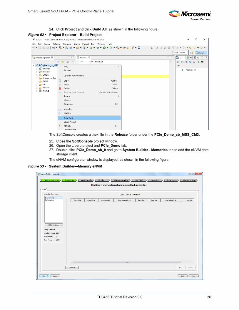
24. Click Project and click Build All, as shown in the following figure.
Figure 52 • Project Explorer—Build Project
The SoftConsole creates a .hex file in the Release folder under the PCIe_Demo_sb_MSS_CM3.
25. Close the SoftConsole project window.26. Open the Libero project and PCIe_Demo tab. 27. Double-click PCIe_Demo_sb_0 and go to System Builder - Memories tab to add the eNVM data
storage client.
The eNVM configurator window is displayed, as shown in the following figure.
Figure 53 • System Builder—Memory eNVM
TU0456 Tutorial Revision 9.0 36

SmartFusion2 SoC FPGA - PCIe Control Plane Tutorial
28. Select Data Storage under the Available Client types tab and click Add to System. The Add Data Storage Client window is displayed, as shown in the following figure.
Figure 54 • Add Data Storage Client
29. Enter Client Name as eNVM in the Add Data Storage Client window.30. Browse for the .hex file generated, as shown in the following figure. The generated executable
image can be found in the Release folder under the SoftConsole project workspace, as shown in the following figure.
Figure 55 • Browsing for .hex File
TU0456 Tutorial Revision 9.0 37

SmartFusion2 SoC FPGA - PCIe Control Plane Tutorial
31. Click OK in the Add Data Storage Client window, as shown in the following figure.
Figure 56 • Add Data Storage Client
32. Click Next and keep the rest of the System Builder tabs as default.
Figure 57 • Modify Core—ENVM
33. Save PCIe_Demo and regenerate the PCIe_Demo component by clicking Generate Component in SmartDesign.
TU0456 Tutorial Revision 9.0 38

SmartFusion2 SoC FPGA - PCIe Control Plane Tutorial
2.7 Step 3: Developing the Simulation StimulusDuring the design process, SERDESIF is configured for the BFM simulation model. The BFM simulation model replaces the entire PCIe interface with a simple BFM that can send write transactions and read transactions over the AHB-Lite interface. These transactions are driven by a file and allow easy simulation of the FPGA design connected to a PCIe interface. This simulation methodology has the benefit of focusing on the FPGA design since the SmartFusion2 PCIe interface is a fully hardened and verified interface.
This section describes how to modify the BFM script (user.bfm) file that is generated by SmartDesign. The BFM script file simulates PCIe writing or reading to or from the MSS through the FIC_0.
1. Open the SERDESIF_0_PCIE_0_user.bfm file. To open the SERDESIF_0_PCIE_0_user.bfm, go to the Files tab > Simulation folder, and double-click the SERDESIF_0_PCIE_0_user.bfm. The SERDESIF_0_PCIE_0_user.bfm file is displayed, as shown in the following figure.
Figure 58 • SmartDesign Generated SERDESIF_0_PCIE_0_user.bfm File
TU0456 Tutorial Revision 9.0 39

SmartFusion2 SoC FPGA - PCIe Control Plane Tutorial
2. Modify the SERDESIF_0_PCIE_0_user.bfm to add the following bfm commands of writing and reading:memmap GPIO 0x40013000;
memmap eSRAM 0x20000000;
procedure main;
# add your BFM commands below:
wait 500us;
wait 500us;
write w GPIO 0x00 0x5;
write w GPIO 0x04 0x5;
write w GPIO 0x08 0x5;
write w GPIO 0x0C 0x5;
write w GPIO 0x10 0x5;
write w GPIO 0x14 0x5;
write w GPIO 0x18 0x5;
write w GPIO 0x1C 0x5;
write w GPIO 0x88 0x00;
write w GPIO 0x88 0x01;
write w GPIO 0x88 0x02;
write w GPIO 0x88 0x04;
write w GPIO 0x88 0x08;
write w GPIO 0x88 0x10;
write w GPIO 0x88 0x20;
write w GPIO 0x88 0x40;
write w GPIO 0x88 0x80;
write w eSRAM 0x00 0x12345678;
write w eSRAM 0x04 0x87654321;
write w eSRAM 0x08 0x9ABCDEF0;
write w eSRAM 0x0C 0x0FEDCBA9;
readcheck w eSRAM 0x00 0x12345678;
readcheck w eSRAM 0x04 0x87654321;
readcheck w eSRAM 0x08 0x9ABCDEF0;
readcheck w eSRAM 0x0C 0x0FEDCBA9;
return
TU0456 Tutorial Revision 9.0 40

SmartFusion2 SoC FPGA - PCIe Control Plane Tutorial
3. The modified BFM file appears similar to the file, as shown in the following figure.BFM commands are added in the SERDESIF_0_PCIE_0_user.bfm. Perform the following:a. Write to MSS GPIO
b. Write to eSRAM
c. Read-check from eSRAM
Figure 59 • Modified SERDES User BFM
TU0456 Tutorial Revision 9.0 41

SmartFusion2 SoC FPGA - PCIe Control Plane Tutorial
2.8 Step 4: Simulating the DesignThe design supports the BFM_PCIe simulation level to communicate with the high-speed serial interface block through the master AXI bus interface. Although, no serial communication actually goes through the High Speed Serial Interface block, this scenario allows validating the fabric interface connections. The SERDESIF_0_PCIE_0_user.bfm file under the <Libero project>/simulation folder contains the BFM commands to verify the read or write access to MSS GPIOs and eSRAM.
The following steps describe how to use the SmartDesign testbench and BFM script file to simulate the design.
1. To generate the HDL testbench file follow the below instructions,a. From the File menu, choose New > HDL Testbench, as shown in the following figure.
Figure 60 • HDL Testbench
Create New HDL Testbench File dialog box is displayed, as shown in the following figure.
Figure 61 • Create New HDL Testbench File
b. Select Verilog or VHDL under HDL Type.
c. Enter testbench as a name of the new HDL testbench file and click OK.
2. Add the wave do file to the PCIe design simulation folder by clicking File > Import > Others.
TU0456 Tutorial Revision 9.0 42

SmartFusion2 SoC FPGA - PCIe Control Plane Tutorial
3. Browse to the wave.do file location in the design files folder:M2S90_PCIE_Control_Demo_DF/Source Files. The following figure shows the wave.do file under simulation folder in the Files window.
Figure 62 • Wave.do File under Simulation Folder
4. Open the Libero SoC project settings (Project > Project Settings).5. Select Do File under Simulation Options in the Project Settings window. Change the Simulation
runtime to 150 us, as shown in the following figure.6. Click Save.
Figure 63 • Project Setting—Do File Simulation Runtime Setting
TU0456 Tutorial Revision 9.0 43

SmartFusion2 SoC FPGA - PCIe Control Plane Tutorial
7. Select Waveforms under Simulation Options, as shown in the following figure:• Select Include Do file.• Select Log all signals in the design.• Click Close to close the Project settings dialog box.• Select Save when prompted to save the changes.
Figure 64 • Project Setting—Waveform
8. To run the simulation, double-click Simulate under Verify Pre-Synthesized Design in the Design Flow window.
TU0456 Tutorial Revision 9.0 44

SmartFusion2 SoC FPGA - PCIe Control Plane Tutorial
ModelSim runs the design for approximately 150 us. The ModelSim transcript window displays the BFM commands and the BFM simulation completed with no errors, as shown in the following figure.
Figure 65 • SERDES BFM Simulation
The following figure shows the waveform window with MSS GPIO output signals.
Figure 66 • Simulation Result with MSS GPIO Signals
TU0456 Tutorial Revision 9.0 45

SmartFusion2 SoC FPGA - PCIe Control Plane Tutorial
2.9 Step 5: Generating the Program FileThe following steps describe how to generate the program file.
1. Double-click Manage Constraints and click Derive Constraints option under Timing tab to generate SDC file for root module. Click Yes to associate SDC file to synthesis, place-and-route and timing verification stages, as shown in the following figures.
Figure 67 • Manage Constraints
Figure 68 • Derive Constraints
Figure 69 • Associate SDC File
TU0456 Tutorial Revision 9.0 46

SmartFusion2 SoC FPGA - PCIe Control Plane Tutorial
2. Click Edit with I/O Editor in constraint manager after completing synthesis, as shown in Figure 70, page 47. The I/O Editor is displayed, make the pin assignments, as shown in the following table. After the pins are assigned, the I/O Editor is displayed, as shown in Figure 71, page 48.
Figure 70 • Edit with I/O Editor
Table 5 • Port to Pin Mapping
Port Name Pin Number
GPIO_0_M2F E1
GPIO_1_M2F F4
GPIO_2_M2F F3
GPIO_3_M2F G7
GPIO_4_M2F H7
GPIO_5_M2F J6
GPIO_6_M2F H6
GPIO_7_M2F H5
GPIO_8_M2F L19
GPIO_9_M2F L18
GPIO_10_M2F K21
GPIO_11_M2F K20
SWITCH J18
PCIE0_PERST_N P18
TU0456 Tutorial Revision 9.0 47

SmartFusion2 SoC FPGA - PCIe Control Plane Tutorial
These pin assignments are for connecting below pins on the SmartFusion2 Security Evaluation Kit.
• GPIO_0 to GPIO_8 for LEDs• GPIO_8 to GPIO_11 for DIP switches• SWITCH for SW4 • PCIE_0_PERST_N to PERST of PCIe Edge connector
Figure 71 • I/O Editor
3. After updating I/O editor, click Commit and Check.4. Close the I/O Editor.5. Click Generate Bitstream, as shown in the following figure to complete place and route, verify
timing, and generate the programming file.
Figure 72 • Generate Bitstream
TU0456 Tutorial Revision 9.0 48

SmartFusion2 SoC FPGA - PCIe Control Plane Tutorial
2.10 Design SetupFollowing steps describe how to program Smartfusion2 Security Evaluation Kit board using Flashpro and how to do design setup:
1. Connect the FlashPro4 programmer to the J5 connector of the SmartFusion2 Security Evaluation Kit board.
2. Connect the jumpers on the SmartFusion2 Security Evaluation Kit board, as shown in the following table.
CAUTION: The power supply switch SW7 on the board should be in OFF position, while making the jumper connections.
3. Connect the power supply to the J6 connector.4. Switch ON the power supply switch, SW7.5. To program the SmarFusion2 device, double-click Run PROGRAM Action in the Design Flow tab,
as shown in the following figure.
Figure 73 • Run PROGRAM Action
6. After Successful programming, power OFF the SmartFusion2 Security Evaluation Kit and shut down the host PC.
7. Following are the steps to connect the CON1-PCIe Edge Connector either to host PC or laptop:a. Connect the CON1-PCIe Edge Connector to host PC PCIe Gen 2 slot or Gen 1 slot, as applicable. If the host PC does not support the Gen 2 compliant slot, the design switches to the Gen 1 slot.
Table 6 • SmartFusion2 FPGA Security Evaluation Kit Jumper Settings
Jumper Pin (From) Pin (To) Comments
J22, J23, J24, J8, J3 1 2 These are the default jumper settings of the SmartFusion2 Security Evaluation Kit board. Ensure, these jumpers are set accordingly.
TU0456 Tutorial Revision 9.0 49

SmartFusion2 SoC FPGA - PCIe Control Plane Tutorial
b. Connect the CON1-PCIe Edge Connector to the laptop PCIe slot using the express card adapter. If you are using a laptop, the express card adapters typically support only Gen 1 and the design works on Gen 1 slot.
CAUTION: Host PC or laptop should be powered OFF while inserting the PCIe Edge Connector. If the system is not powered OFF, the PCIe device detection and selection of Gen 1 or Gen 2 does not occur properly. Microsemi recommends that the host PC or laptop should be powered OFF during the PCIe card insertion.
The board setup is as shown in the following figure.
Figure 74 • SmartFusion2 Security Evaluation Kit Setup
8. Switch ON the power supply switch, SW7.
2.11 Running the DesignThis tutorial can run on both windows and Red Hat Linux operating system.
To run the tutorial on Windows operating system GUI, Microsemi PCIe drivers are provided. Refer to Running the Design on Windows, page 51.
To run the tutorial on Linux operating system native Red Hat Linux drivers and command line scripts are provided. Refer to Running the Design on Linux, page 59.
TU0456 Tutorial Revision 9.0 50

SmartFusion2 SoC FPGA - PCIe Control Plane Tutorial
2.11.1 Running the Design on WindowsThe following steps describe how to run the demo design on Windows:
1. Switch ON the power supply switch, SW7.2. Power on the host PC and open the host PC Device Manager for PCIe device, as shown in the
following figure. If the PCIe device is not detected, power cycle the SmartFusion2 Security Evaluation Kit board.
3. Right-click PCI Device > scan for hardware changes in Device Manager.
Figure 75 • Device Manager—PCIe Device Detection
Note: If the device is still not detected, check if the BIOS in host PC is the latest version, and if PCI is enabled in the host PC BIOS.
TU0456 Tutorial Revision 9.0 51

SmartFusion2 SoC FPGA - PCIe Control Plane Tutorial
2.11.1.1 Drivers Installation Perform the following steps to install the PCIe drivers on the host PC:
1. Right-click PCI Device in Device Manager and select Update Driver Software..., as shown in the following figure. To install the drivers, administrative rights are required.
Figure 76 • Update Driver Software
2. In the Update Driver Software - PCIe Device window, select the Browse my computer for driver software option as shown in the following figure.
Figure 77 • Browse for Driver Software
TU0456 Tutorial Revision 9.0 52

SmartFusion2 SoC FPGA - PCIe Control Plane Tutorial
3. Browse the drivers folder: M2S90_PCIe_Control_Plane_DF\Windows_64bit\Drivers\PCIe_Demo and click Next, as shown in the following figure.
Figure 78 • Browse for Driver Software Continued
4. The Windows Security dialog box is displayed. Click Install as shown in the following figure. After successful driver installation, a message appears. See Figure 80, page 53.
Figure 79 • Windows Security
Figure 80 • Successful Driver Installation
TU0456 Tutorial Revision 9.0 53

SmartFusion2 SoC FPGA - PCIe Control Plane Tutorial
2.11.1.2 PCIe Demo GUI Installation SmartFusion2 PCIe GUI is a simple graphic user interface that runs on the host PC to communicate with the SmartFusion2 PCIe endpoint device. The GUI provides the PCIe link status, driver information, and demo controls. The GUI invokes the PCIe driver installed on the host PC and provides commands to the driver according to the user selection.
To install the GUI:
1. Extract the PCIe_Demo_GUI_Installer.rar and locate the files atM2S90_PCIe_Control_Plane_DF\GUI
2. Double-click setup.exe in the provided GUI installation (PCIe_Control_Plane_Demo_GUI_Installer\setup.exe). Apply default options, as shown in the following figure.
3. To start the installation, click Next.
Figure 81 • GUI Installation
4. Click Finish to complete the installation.
Figure 82 • Successful GUI Installation
5. Restart the host PC.
TU0456 Tutorial Revision 9.0 54

SmartFusion2 SoC FPGA - PCIe Control Plane Tutorial
2.11.1.3 Running the PCIe GUIThe following steps describe how to run the PCIe GUI:
1. Check the host PC Device Manager for the drivers. If the device is not detected, power cycle the SmartFusion2 Security Evaluation Kit board.
2. Click scan for hardware changes in Device Manager window. Ensure that the board is switched on.
Figure 83 • Device Manager—PCIe Device Detection
Note: If a warning symbol is displayed on the Microsemi PCIe in the Device Manager, uninstall them and start from step1 of Drivers Installation, page 59.
3. Invoke the GUI from ALL Programs > PCIe Control Plane Demo. The GUI is displayed, as shown in the following figure.
Figure 84 • PCIe Demo GUI
TU0456 Tutorial Revision 9.0 55

SmartFusion2 SoC FPGA - PCIe Control Plane Tutorial
4. Click Connect. The application detects and displays the information related to the connected kit such as Device Vendor ID, Device Type, Driver Version, Driver Time Stamp, Demo Type, Supported Width, Negotiated Width, Supported Speed, Negotiated Speed, Number of Bars, and BAR Address as shown in the following figure.
Figure 85 • Device Info
5. Click the Demo Controls tab to display the LED Controls, DIP Switch Status, and Interrupt Counters as shown in the following figure.
Figure 86 • Demo Controls
TU0456 Tutorial Revision 9.0 56

SmartFusion2 SoC FPGA - PCIe Control Plane Tutorial
6. Click Start LED ON/OFF Walk, Enable DIP SW Session, and Enable Interrupt Session to view controlling LEDs, getting the DIP switch status, and monitoring the interrupts simultaneously as shown in the following figure.
Figure 87 • Demo Controls—Continued
7. Click Config Space to view details about the PCIe configuration space. The following figure shows the PCIe configuration space.
Figure 88 • Configuration Space
TU0456 Tutorial Revision 9.0 57

SmartFusion2 SoC FPGA - PCIe Control Plane Tutorial
8. Click the PCIe Read/Write tab to perform read and writes to LSRAM memory through BAR1 space. Click Read to read the 4 KB memory mapped to BAR1 space as shown in the following figure.
Figure 89 • PCIe BAR1 Memory Access
9. Click Exit to quit the demo.
TU0456 Tutorial Revision 9.0 58

SmartFusion2 SoC FPGA - PCIe Control Plane Tutorial
2.11.2 Running the Design on LinuxThe following steps describe how to run the Design on Linux.
1. Switch ON the Red Hat Linux host PC.2. Red Hat Linux Kernel detects the SmartFusion2 PCIe endpoint as Actel Device.3. On Linux Command Prompt Use lspci command to display the PCIe info.
# lspci
Figure 90 • PCIe Device Detection
2.11.2.1 Drivers InstallationEnter the following commands in the Linux command prompt to install the PCIe drivers:
1. Create the sf2 directory under the home/ directory using the following command:# mkdir /home/sf2
2. Copy the M2S90_PCIe_Control_Plane_DF design files folder under /home/sf2 directory, which contains the Linux PCIe device driver files and Linux PCIe application utility files.
3. Copy the Linux PCIe Device Driver file (PCIe_Driver.rar) from M2S90_PCIe_Control_Plane_DF/design files folder.cp -rf/home/sf2/M2S90_PCIe_Control_Plane_DF/Linux_64bit/Drivers/PCIe_Driver.rar /home/sf2# unrar -e PCIe_Driver.rar
4. Execute ls command to display the contents of /home/sf2 directory.# ls
5. Change to inc/ directory by using the following command:#cd /home/sf2/inc
TU0456 Tutorial Revision 9.0 59

SmartFusion2 SoC FPGA - PCIe Control Plane Tutorial
6. Edit the board.h file for SmartFusion2 Security Evaluation Kit, as shown in the following figure.#vi board.h
#undef SF2_ADV_KIT
#undef IGL2
#undef SF2_DEV_KIT
#define SF2_EVAL_KIT
Figure 91 • Edit board.h File
7. To save the selected file, execute the :wq command8. Change to PCIe_Driver/ directory using the cd command:
#cd /home/sf2/PCIe_Driver9. To compile the Linux PCIe device driver code, execute make command.
#make clean [To clean any *.o, *.ko files]#make
10. The kernel module, pci_chr_drv_ctrlpln.ko creates in the same directory.11. To insert the Linux PCIe device driver as a module, execute insmod command.
#insmod pci_chr_drv_ctrlpln.ko Note: Root privileges are required to execute this command.
Figure 92 • PCIe Device Driver Installation
TU0456 Tutorial Revision 9.0 60

SmartFusion2 SoC FPGA - PCIe Control Plane Tutorial
12. After successful Linux PCIe device driver installation, check /dev/MS_PCI_DEV got created by using the following Linux command:#ls /dev/MS_PCI_DEV
Note: /dev/MS_PCI_DEV interface is used to access the SmartFusion2 PCIe end point from Linux user space.
2.11.2.2 Linux PCIe Application Compilation and PCIe Control Plane Utility Creation1. Change to the /home/sf2/ directory using the following command:
#cd /home/sf22. Copy the M2S90_PCIE_Control_DEMO_DF\Linux_64bit\Util\PCIe_App folder from the Windows
host PC and place it into the /home/sf2 directory of RedHat Linux host PC.3. Change to the /home/sf2/PCIe_App directory using the following command:
#cd /home/sf2/PCIe_App4. Compile the Linux user space application pcie_appln_ctrlpln.c by using gcc command.
#gcc -o pcie_ctrlplane pcie_appln_ctrlpln.c
Figure 93 • Linux PCIe Application Utility
5. After successful compilation, Linux PCIe application utility pcie_ctrlplane creates in the same directory.
6. On Linux Command Prompt run the pcie_ctrlplane utility as:#./pcie_ctrlplane Help menu displays, as shown in the preceding figure.
TU0456 Tutorial Revision 9.0 61

SmartFusion2 SoC FPGA - PCIe Control Plane Tutorial
2.11.2.3 Execution of Linux PCIe Control Plane Features
2.11.2.3.1 LED ControlLED1 to LED8 is controlled by writing data to SmartFusion2 LED Control Registers.
#./pcie_ctrlplane 1 0x000000FF [LED OFF]
#./pcie_ctrlplane 1 0x00000000 [LED ON]
Figure 94 • Linux Command—LED Control
led_blink.sh, contains the shell script code to perform LED Walk ON where as Ctrl C exits the shell script and LED Walk turns OFF.
Run the led_blink.sh shell script using sh command.
#sh led_blink.sh
TU0456 Tutorial Revision 9.0 62

SmartFusion2 SoC FPGA - PCIe Control Plane Tutorial
2.11.2.3.2 SRAM Read/Write64 KB SRAM is accessible for SmartFusion2 Security Evaluation Kit.
#./pcie_ctrlplane 2 1 0xFF00FF00 0x1000 [SRAM WRITE]
#./pcie_ctrlplane 3 0 0x1000 [SRAM READ]
Figure 95 • Linux Command—SRAM Read/Write
TU0456 Tutorial Revision 9.0 63

SmartFusion2 SoC FPGA - PCIe Control Plane Tutorial
2.11.2.3.3 DIP Switch StatusDip Switch on SmartFusion2 Security Evaluation Kit consists of four electric switches to hold the device configurations. Linux PCIe utility reads the corresponding switches (ON/OFF) state.
#./pcie_ctrlplane 4 [DIP Switch Status]
Figure 96 • Linux Command—DIP Switch
TU0456 Tutorial Revision 9.0 64

SmartFusion2 SoC FPGA - PCIe Control Plane Tutorial
2.11.2.3.4 PCIe Configuration Space DisplayPCIe Configuration Space contains the PCIe device data, such as Vendor ID, Device ID, and Base Address 0.
Note: Root Privileges are required to execute this command.
#./pcie_ctrlplane 5 1 [Read PCIe Configuration Space]
Figure 97 • Linux Command—PCIe Configuration Space Display
TU0456 Tutorial Revision 9.0 65

SmartFusion2 SoC FPGA - PCIe Control Plane Tutorial
2.11.2.4 PCIe Link Speed and WidthNote: Root Privileges are required to execute this command.
#./pcie_ctrlplane 5 2 [Read PCIe Link Speed and Link Width]
Figure 98 • Linux Command—PCIe Link Speed and Width
TU0456 Tutorial Revision 9.0 66

SmartFusion2 SoC FPGA - PCIe Control Plane Tutorial
Figure 99 • Linux Command—PCIe Link Speed and Width
TU0456 Tutorial Revision 9.0 67

SmartFusion2 SoC FPGA - PCIe Control Plane Tutorial
2.11.2.4.1 PCIe Interrupt Control (Enable/Disable) and Interrupt CounterSmartFusion2 Security Evaluation Kit enable or disable the MSI interrupts by writing data to its PCIe configuration space.
Interrupt Counter holds the number of MSI interrupts got triggered by pressing the SW4 Push button.
#. /pcie_ctrlplane 6 0 [Disable Interrupts]
#. /pcie_ctrlplane 6 1 [Enable Interrupts]
#. /pcie_ctrlplane 7 [Interrupt Counter Value]
Figure 100 • Linux Command—PCIe Interrupt Control
2.12 ConclusionThis tutorial describes how to access the PCIe endpoint features of SmartFusion2, create a simple design, and verify the design using BFM simulation. This tutorial demonstrates that the host PC can easily communicate with the SmartFusion2 Security Evaluation Kit through the provided GUI and Drivers. This tutorial also provides a Linux PCIe application for accessing PCIe endpoint device through Linux PCIe Device Driver.
TU0456 Tutorial Revision 9.0 68