Trust-Based Design and Check of FPGA Circuits Using …dutt/papers/acm-trets.pdfTrust-Based Design...
33
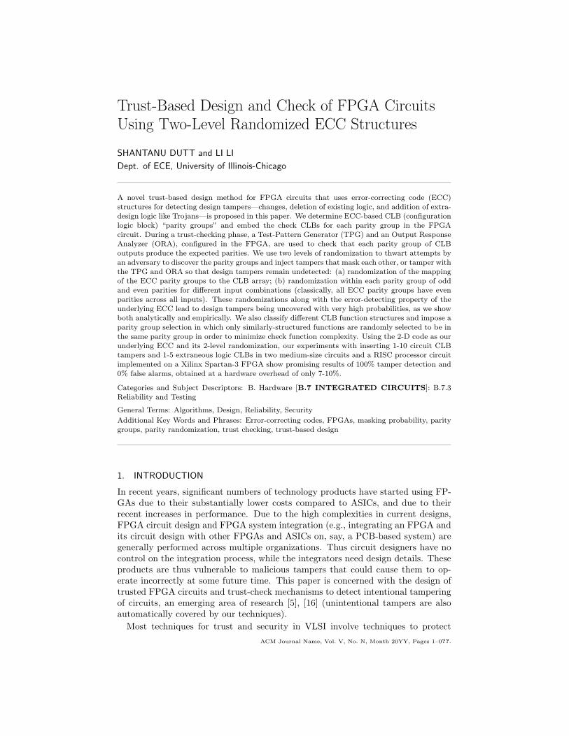
Trust-Based Design and Check of FPGA Circuits Using Two-Level Randomized ECC Structures SHANTANU DUTT and LI LI Dept. of ECE, University of Illinois-Chicago A novel trust-based design method for FPGA circuits that uses error-correcting code (ECC) structures for detecting design tampers—changes, deletion of existing logic, and addition of extra- design logic like Trojans—is proposed in this paper. We determine ECC-based CLB (configuration logic block) “parity groups” and embed the check CLBs for each parity group in the FPGA circuit. During a trust-checking phase, a Test-Pattern Generator (TPG) and an Output Response Analyzer (ORA), configured in the FPGA, are used to check that each parity group of CLB outputs produce the expected parities. We use two levels of randomization to thwart attempts by an adversary to discover the parity groups and inject tampers that mask each other, or tamper with the TPG and ORA so that design tampers remain undetected: (a) randomization of the mapping of the ECC parity groups to the CLB array; (b) randomization within each parity group of odd and even parities for different input combinations (classically, all ECC parity groups have even parities across all inputs). These randomizations along with the error-detecting property of the underlying ECC lead to design tampers being uncovered with very high probabilities, as we show both analytically and empirically. We also classify different CLB function structures and impose a parity group selection in which only similarly-structured functions are randomly selected to be in the same parity group in order to minimize check function complexity. Using the 2-D code as our underlying ECC and its 2-level randomization, our experiments with inserting 1-10 circuit CLB tampers and 1-5 extraneous logic CLBs in two medium-size circuits and a RISC processor circuit implemented on a Xilinx Spartan-3 FPGA show promising results of 100% tamper detection and 0% false alarms, obtained at a hardware overhead of only 7-10%. Categories and Subject Descriptors: B. Hardware [B.7 INTEGRATED CIRCUITS]: B.7.3 Reliability and Testing General Terms: Algorithms, Design, Reliability, Security Additional Key Words and Phrases: Error-correcting codes, FPGAs, masking probability, parity groups, parity randomization, trust checking, trust-based design 1. INTRODUCTION In recent years, significant numbers of technology products have started using FP- GAs due to their substantially lower costs compared to ASICs, and due to their recent increases in performance. Due to the high complexities in current designs, FPGA circuit design and FPGA system integration (e.g., integrating an FPGA and its circuit design with other FPGAs and ASICs on, say, a PCB-based system) are generally performed across multiple organizations. Thus circuit designers have no control on the integration process, while the integrators need design details. These products are thus vulnerable to malicious tampers that could cause them to op- erate incorrectly at some future time. This paper is concerned with the design of trusted FPGA circuits and trust-check mechanisms to detect intentional tampering of circuits, an emerging area of research [5], [16] (unintentional tampers are also automatically covered by our techniques). Most techniques for trust and security in VLSI involve techniques to protect ACM Journal Name, Vol. V, No. N, Month 20YY, Pages 1–0??.
Transcript of Trust-Based Design and Check of FPGA Circuits Using …dutt/papers/acm-trets.pdfTrust-Based Design...
Trust-Based Design and Check of FPGA CircuitsUsing Two-Level Randomized ECC Structures
SHANTANU DUTT and LI LI
Dept. of ECE, University of Illinois-Chicago
A novel trust-based design method for FPGA circuits that uses error-correcting code (ECC)
structures for detecting design tampers—changes, deletion of existing logic, and addition of extra-design logic like Trojans—is proposed in this paper. We determine ECC-based CLB (configuration
logic block) “parity groups” and embed the check CLBs for each parity group in the FPGA
circuit. During a trust-checking phase, a Test-Pattern Generator (TPG) and an Output ResponseAnalyzer (ORA), configured in the FPGA, are used to check that each parity group of CLB
outputs produce the expected parities. We use two levels of randomization to thwart attempts by
an adversary to discover the parity groups and inject tampers that mask each other, or tamper withthe TPG and ORA so that design tampers remain undetected: (a) randomization of the mapping
of the ECC parity groups to the CLB array; (b) randomization within each parity group of odd
and even parities for different input combinations (classically, all ECC parity groups have evenparities across all inputs). These randomizations along with the error-detecting property of the
underlying ECC lead to design tampers being uncovered with very high probabilities, as we showboth analytically and empirically. We also classify different CLB function structures and impose a
parity group selection in which only similarly-structured functions are randomly selected to be in
the same parity group in order to minimize check function complexity. Using the 2-D code as ourunderlying ECC and its 2-level randomization, our experiments with inserting 1-10 circuit CLB
tampers and 1-5 extraneous logic CLBs in two medium-size circuits and a RISC processor circuit
implemented on a Xilinx Spartan-3 FPGA show promising results of 100% tamper detection and0% false alarms, obtained at a hardware overhead of only 7-10%.
Categories and Subject Descriptors: B. Hardware [B.7 INTEGRATED CIRCUITS]: B.7.3Reliability and Testing
General Terms: Algorithms, Design, Reliability, Security
Additional Key Words and Phrases: Error-correcting codes, FPGAs, masking probability, parity
groups, parity randomization, trust checking, trust-based design
1. INTRODUCTION
In recent years, significant numbers of technology products have started using FP-GAs due to their substantially lower costs compared to ASICs, and due to theirrecent increases in performance. Due to the high complexities in current designs,FPGA circuit design and FPGA system integration (e.g., integrating an FPGA andits circuit design with other FPGAs and ASICs on, say, a PCB-based system) aregenerally performed across multiple organizations. Thus circuit designers have nocontrol on the integration process, while the integrators need design details. Theseproducts are thus vulnerable to malicious tampers that could cause them to op-erate incorrectly at some future time. This paper is concerned with the design oftrusted FPGA circuits and trust-check mechanisms to detect intentional tamperingof circuits, an emerging area of research [5], [16] (unintentional tampers are alsoautomatically covered by our techniques).
Most techniques for trust and security in VLSI involve techniques to protectACM Journal Name, Vol. V, No. N, Month 20YY, Pages 1–0??.
2 ·
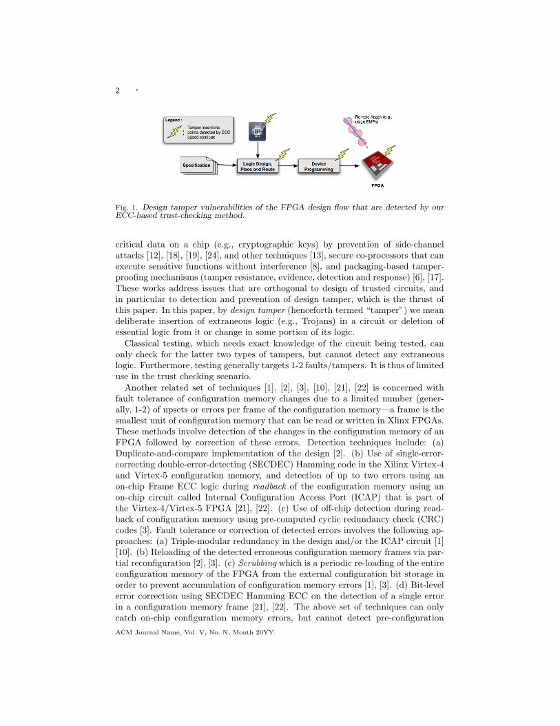
Fig. 1. Design tamper vulnerabilities of the FPGA design flow that are detected by ourECC-based trust-checking method.
critical data on a chip (e.g., cryptographic keys) by prevention of side-channelattacks [12], [18], [19], [24], and other techniques [13], secure co-processors that canexecute sensitive functions without interference [8], and packaging-based tamper-proofing mechanisms (tamper resistance, evidence, detection and response) [6], [17].These works address issues that are orthogonal to design of trusted circuits, andin particular to detection and prevention of design tamper, which is the thrust ofthis paper. In this paper, by design tamper (henceforth termed “tamper”) we meandeliberate insertion of extraneous logic (e.g., Trojans) in a circuit or deletion ofessential logic from it or change in some portion of its logic.
Classical testing, which needs exact knowledge of the circuit being tested, canonly check for the latter two types of tampers, but cannot detect any extraneouslogic. Furthermore, testing generally targets 1-2 faults/tampers. It is thus of limiteduse in the trust checking scenario.
Another related set of techniques [1], [2], [3], [10], [21], [22] is concerned withfault tolerance of configuration memory changes due to a limited number (gener-ally, 1-2) of upsets or errors per frame of the configuration memory—a frame is thesmallest unit of configuration memory that can be read or written in Xlinx FPGAs.These methods involve detection of the changes in the configuration memory of anFPGA followed by correction of these errors. Detection techniques include: (a)Duplicate-and-compare implementation of the design [2]. (b) Use of single-error-correcting double-error-detecting (SECDEC) Hamming code in the Xilinx Virtex-4and Virtex-5 configuration memory, and detection of up to two errors using anon-chip Frame ECC logic during readback of the configuration memory using anon-chip circuit called Internal Configuration Access Port (ICAP) that is part ofthe Virtex-4/Virtex-5 FPGA [21], [22]. (c) Use of off-chip detection during read-back of configuration memory using pre-computed cyclic redundancy check (CRC)codes [3]. Fault tolerance or correction of detected errors involves the following ap-proaches: (a) Triple-modular redundancy in the design and/or the ICAP circuit [1][10]. (b) Reloading of the detected erroneous configuration memory frames via par-tial reconfiguration [2], [3]. (c) Scrubbing which is a periodic re-loading of the entireconfiguration memory of the FPGA from the external configuration bit storage inorder to prevent accumulation of configuration memory errors [1], [3]. (d) Bit-levelerror correction using SECDEC Hamming ECC on the detection of a single errorin a configuration memory frame [21], [22]. The above set of techniques can onlycatch on-chip configuration memory errors, but cannot detect pre-configurationACM Journal Name, Vol. V, No. N, Month 20YY.

· 3
tampering of the FPGA design/configuration bits—the main focus of this paper.Further, unless a time consuming bit-by-bit comparison is performed of the read-back configuration memory frames with the frames of the original configuration bits(stored off-chip), these techniques can only catch a few errors in each frame. Thusthese fault-tolerance oriented approaches are not very germane to trust design andchecking.
Recently, [16] addressed various issues in the protection of FPGA designs fromtampering. It argues that: i) FPGA chip fabrication is completely separated fromFPGA circuit design, so there is no scope for an adversary at the fabrication com-pany to tamper with any circuit design; ii) FPGA configuration bitstreams are hardto reverse engineer in order for an adversary to determine the circuit and tamperwith it; iii) the bitstream can be further protected by encrypting it, and decryptionhardware is available in many current FPGAs for internal decryption of bitstreams.While the first point is correct, the circuit design could be required at an integrationcompany (as opposed to at the fabrication company) that assembles, for example,application-specific multi-chip PCBs that include FPGAs, in which the designs areneeded to test and fine-tune the product. This exposes the designs to an adversaryat such a company. Furthermore, bit-stream reverse-engineering while hard, is notimpossible for a determined adversary as is acknowledged in [16]. Finally, whileencryption provides a reasonable trusted FPGA design execution environment, itimposes certain restrictions on FPGA use like disabling of partial reconfiguration[16], and is thus not suitable for applications such as adaptive computing, an im-portant niche area for FPGAs. Furthermore, encryption does not protect againsttampered IPs that are unknowingly used in an otherwise trustworthy design.
Another possible trust-design approach is signature computation and checking ofthe bitstream. In this approach, a signature S of the bitstream is computed (e.g.,using a linear-feedback shift-register [LFSR] based computation) on the “golden”(correct) FPGA bitstream and sent directly to the user. When the FPGA, pos-sibly integrated on a PCB with other components, arrives at the user’s location,he/she needs to compute the signature S of the FPGA circuit’s bitstream (that is,for example, stored on a ROM). If S 6= S, then this indicates presence of tampersin the new bitstream. There are two drawbacks to the signature-checking scheme.One, signature checking is an off-chip checking approach, and thus cannot protectagainst malicious IPs (since IPs are encrypted), tampers introduced by the deviceprogramming unit or against remote attacks like those using high-energy electro-magnetic pulses (EMPs) that tamper the on-chip configuration bits. Secondly, inthe case of checking only the design configuration bits, even using strong signaturecomputation techniques like LFSR, their non-detection probability (equal to thealiasing—two distinct bitstreams producing the same signature—probability) is anorder of magnitude higher than ours. For example, as we show in Sec. 2, for amedium-size FPGA like the Spartan-3 with a 24×20 CLB array, our non-detection(or masking) probability is ≈ 16×10−9. In [14] it has been shown that in the contextof testing circuits with one output bit, in which the output bits across input vectorsto the circuit are compacted into a signature using an LFSR approach, the aliasingprobability is lower bounded by 1/L if the signature register period is greater thanL, where L is the number of random test inputs (in other words L is the number of
ACM Journal Name, Vol. V, No. N, Month 20YY.

4 ·
output bits compacted). Translating this to the signature computation of an FPGAwith a configuration bit size of L, we get a lower bound for the aliasing probabilityof 1/L. Large Virtex-4 FPGAs have L of the order of 5M-50M bits [21], and we thusestimate that the L for the smaller Spartan-3 FPGA with a 24×20 CLB array is atmost 5M bits (we could not find the configuration bit size of this FPGA), leading toan aliasing probability lower bound of 2 × 10⁻⁷. The non-detection probability ofour ECC based technique for the above Spartan-3 FPGA is thus about 12.5 timesless than what would be obtained by an LFSR-based signature computation andchecking approach for FPGA trust verification. This, coupled with the fact thatour technique can detect tampers in many scenarios in which signature checking isineffective, makes our ECC based on-chip checking approach superior.
Figure 1 shows four different tamper vulnerability points of an FPGA circuit (de-sign, IP, device programming and remote attacks using, say, high-energy EMPs)that are not all protected by fault tolerance, signature-checking or encryption ap-proaches. Thus it is necessary to employ explicit trust design and checking tech-niques for FPGA circuits that: (1) check the circuit’s configuration bits on-chip,and (2) are functionality-based, which allows all the four vulnerabilities to be ad-dressed. The techniques presented in this paper are of this type. Such methods alsoenable FPGAs to be used in a trusted manner in all types of applications withoutrestrictions on the use of any of their features.
In this paper we address design tampering of FPGA circuits’ logic elements, i.e.,the CLBs. Trust design and verification for tampering of interconnect routing willbe addressed in a future paper. We assume the following in our trust design andcheck methodology:
(1) The original design process of the FPGA circuit is trusted.(2) Either the correct original design (the “golden reference”) is available for sub-
sequent trust-based design (trust structure insertions) or trust-based designimmediately follows the original design phase (thus almost eliminating anypossibility of any design tamper between the original design and trust-baseddesign phases).
We also note that we do not need the golden reference during trust verifica-tion/checking.
The rest of the paper is organized as follows. Section 2 presents the basic ideaof ECC-based trust-checking for design-tamper detection in FPGA circuits. Sec-tion 3 gives an introduction to the Spartan-3 FPGA architecture for which we haveinstantiated our techniques. Section 4 discusses TPG control of inaccessible inputsof CLB logic and determination of the TPG size needed to check a given circuit. InSec. 5, we give a classification of logic structures of slices (a slice is a smaller logicunit within a CLB, which has multiple slices; see Sec. 3) called parity group patternsthat is useful for determining parity groups with similarly structured slice outputsthat yield low check-CLB/slice overhead. Next, in Sec. 6 we discuss and analyzetechniques for tackling tampers in the checker circuit (TPG and ORA) that use asecond level of randomization, that of the parity vectors of parity groups. Section 7discusses different embeddings of the check components in an FPGA and their at-tendant hardware overheads. In Sec. 8 we present our experimental results, and weconclude in Sec. 9.ACM Journal Name, Vol. V, No. N, Month 20YY.

· 5
Fig. 2. (a) A 2D code on information bits. (b) An FPGA circuit with embedded structural2D code; each row and column is a parity group of CLBs.
pass/fail
Parity group(under test)
pass/fail
Check PLBs
row Ricol Cj
C0,1 C0,2 C0,3C0,0
C1,1 C1,2 C1,3C1,0
C2,1 C2,2 C2,3C2,0
C3,1 C3,2 C3,3C3,0 x
R2
R1
C1 C2 C3 C4
R3
R4
(a) (b)
C0,1 C0,2 C0,30,0
C1,1 C1,2 C1,31,0
C2,1 C2,2 C2,3C2,0
C3,1 C3,2 C3,3C3,0 x
C
C
TPG ORATPG ORA
Fig. 3. (a) A 2 × 2 masking pattern of 4 tampers shown by X’s. (b) A random mappingof a 2D code to the CLB array (the ECC’s column and row parity groups are shown bysolid and dashed lines, respectively).
2. ECC-BASED DESIGN-TAMPER DETECTION
Our core idea in designing trusted FPGA circuits is to impose an ECC’s paritygroup structure on the CLB array. During a trust-checking phase, a Test-PatternGenerator (TPG) is connected to the inputs of each parity group (PG) of CLBs,one at a time, and feeds identical input/test vectors to each CLB in a group, whilean Output Response Analyzer (ORA) determines the parity of the outputs of theCLBs in the PG for each test vector1; see Fig. 2(b). The output vector produced
1It is also possible to check multiple PGs at a time by connecting the TPG outputs to all theirinputs, and using separate ORAs to check each PG; the number k of PGs that can be checked
simultaneously is limited only by the FPGA size and the resources needed by k ORAs. For
ACM Journal Name, Vol. V, No. N, Month 20YY.

6 ·
Fig. 4. Our ECC-based trust checking flow.
by the ORA (the ORA produces a parity bit per test vector) is then checked todetermine if it is the expected parity vector (PV) for this PG; for the even parityscheme we have discussed so far this PV will be the zero vector, but for the random-parity technique to be discussed in Sec. 6, the PV will be a pre-determined randombit vector. For example, consider a PG with 2-input functions, with input vectorsI0, I1, I2, I3, and a randomly determined parity of (odd, even, even, odd) acrossthese input vectors. Then the expected PV for this PG is (1,0,0,1). If, on the otherhand, we use the even parity scheme, then this PG’s expected PV = (0, 0, 0, 0).
In either parity schemes (even or random), if the ORA output is the expectedPV, then the CLBs in this group are tamper-free with very high probability (aswe will establish shortly, both analytically and empirically). The entire FPGA istamper-free with very high probability if all PGs are determined to be tamper-free;otherwise, the FPGA is determined to have tampers. Figure 4 shows our trustchecking flow for Xilinx FPGAs that uses the Xilinx ISE toolset.
Classically, in ECCs the designed-for parity is always even, and the rest of thisdiscussion, unless otherwise stated, is based on even-parity groups in the FPGA
simplicity of exposition, we assume henceforth, unless otherwise stated, that one PG is checked
at a time.
ACM Journal Name, Vol. V, No. N, Month 20YY.

· 7
Fig. 5. Arrangement of slices within a CLB [20].
circuit; in Sec. 6, we augment our method with random parities across input vectorsof a PG. Any deviation from the expected parity, implies some tampering of theCLB logic for one or more outputs in that group.
In an ECC for information bits, for the ith parity group, there is a check bit Ci
and k information bits xi,1, . . . , xi,k, where
ci = xi,1 ⊕ xi,2...⊕ xi,k = XORkj=1xi,j (1)
Figure 2(a) shows a 2D parity code in which the information bits and check bits arearranged in a 2D matrix, with the check bits occupying the last row and column;each row and column of this matrix defines a parity group. Similar to bits, CLBscan also be arranged in parity groups, where circuit CLB outputs correspond toinformation bits and check CLB outputs to check bits. The output function of thecheck CLB in each PG is then the parity or XOR of the output functions of thecircuit CLBs in the PG. Figure 2(b) shows a 2D code overlaid on the CLB array ofan FPGA.
Assuming for the moment that there is one output per CLB, in the 2D phys-ical arrangement of Fig. 2(b), the output of column check CLBs CC(3, i) is thefunction CC(3, i) = XOR2
j=0C(j, i), where C(j, i) is used here to denote the out-put function of the CLB that is also labeled as C(j, i); similarly for the row-checkCLBs CC(i, 3)’s. As mentioned earlier, tamper detection is performed by a TPGgenerating all possible input vectors that simultaneously feed all CLBs in a paritygroup, and an ORA determining if the parity of the CLBs’ outputs (that are in thesame parity group) is even across all input vectors.
We note that we always need to map the underlying ECC to the entire CLBarray of the FPGA, irrespective of whether a CLB is part of the functional circuitor not. This is needed in order to detect the presence of extraneous logic insertedinto non-functional CLBs/slices. We also configure all non-functional CLBs/slicesto implement the zero function (one whose output is always logic 0). The reasonfor this is that for an extraneous circuit to disrupt the application circuit, all itsCLBs/slices cannot be configured with zero functions, as otherwise it would donothing (e.g., there at least needs to be a multiplexer in the extraneous circuit to
ACM Journal Name, Vol. V, No. N, Month 20YY.

8 ·
connect one of its outputs to at least one input of some slice/CLB of the applicationcircuit in order to disrupt it, and the multiplexer output will be a non-zero function).Hence at least some CLB output of the extraneous circuit would have to be a non-zero function for this to be possible. Since this is a change to its “normal” zero-function output, and since we check the entire CLB array during the trust-checkingphase, any extraneous circuit insertions will be detected by our techniques withhigh probability2.
Randomization of Parity Group Mapping: In an adversarial design tampering sce-nario (as opposed to one of randomly occurring faults), having an obvious mappingof the 2D code to the CLB array can be easily defeated by arranging tampers in a2 × 2 subarray in which they “mask” each other (masking is formally defined anddiscussed shortly); see Fig. 3(a). The way around this problem is to randomizethe mapping of the m × n 2D parity code onto an m × n CLB array. In otherwords, if r : H × V → H × V is a random function, where H = {0, . . . ,m − 1}is the set of row coordinates and V = {0, . . . , n − 1} is the set of column coordi-nates, then the i’th row X(i, 0), . . . , X(i, n− 1) of the 2D code is mapped to CLBsC(r(i, 0)), . . . , C(r(i, n− 1)), and similarly its j’th column X(0, j), . . . , X(m− 1, j)is mapped to CLBs C(r(0, j)), . . . , C(r(m − 1, j)); a random mapping is shown inFig. 3(b). It is virtually impossible for an adversary to determine the randomizedembedding of a 2D code (or of any other ECC) into the CLB array unless he/sheexhaustively analyzes all subsets of CLB outputs and determines if for each subsetone of the outputs is the parity of the others. Note that it will be necessary for anadversary to examine all subsets of CLBs (as opposed to subsets of sizes m and nonly), since it is not necessary that we only map an m × n 2D code to the m × nCLB array; any m′ × n′ 2D code can be mapped to this array, where m′n′ ≥ mn,m′(n′ − 1) < mn and (m′ − 1)n′ < mn. This means analyzing 2mn subsets, avirtually impossible task for current FPGAs which have mn in the order of 64 to20,000.
Tamper Masking: In an ECC for information bits, the flipping of two bits in thesame parity group avoids detection in the PG (but not necessarily in the entireECC, since these two flipped bits could also be present in other disjoint paritygroups, where their errors can be detected if no other bits have flipped in thesegroups). Such a phenomenon of non-detection due to multiple bit errors is calledmasking—in such cases the errors are said to mask each other. Similarly, maskingcan occur in CLB PGs due to multiple tampers, so that across all test vectors theoutput parities of a PG with tampers remain unchanged. Let fi1 , . . . , fit
be CLBoutputs that belong to the same PG, and let there be tampers in the CLB logicused to generate these outputs. We denote the tampered outputs by fi1 , . . . , fit
.These tampered outputs are said to mask each other if:
XORtj=1fij = XORt
j=1fij , (2)
since under this condition, it is clear that these tampers will not change the parity
2The tampered connection structure to the input(s) of some application circuit CLBs can alsobe detected by route tamper detection for which we have recently developed some techniques. A
discussion of route tamper detection is, however, beyond the scope of this paper.
ACM Journal Name, Vol. V, No. N, Month 20YY.

· 9
of the PG for any test vector.We have been able to determine two general approaches to inserting tampers
that mask each other in a PG:
(1) If there are two or more identical output functions in a PG, then insertingidentical tampers in an even number of them will cause them to mask each other.Thus if fi1 , . . . , fis
are identical and s is even, then XORsj=1fij
= 0 (a ⊕ a = 0—we will use the operators XOR and ⊕ interchangeably to denote the exclusive-oroperation). If their tampers are also identical, then the corresponding tamperedfunctions fij
’s are also identical. Thus we also have XORsj=1fij
= 0, and Eqn. 2will be satisfied.
(2) Inserting tampers in an even number of outputs in a PG so that each outputfunction is complemented also causes the tampers to mask each other. Since a⊕b =a⊕ b, we satisfy Eqn. 2 if the number s of outputs tampered in this manner is even.
From the second masking tamper pattern, one can extrapolate the following ECC-oblivious scheme for tampering all functional outputs of CLBs such that they arenever detected in our ECC based technique: complement all CLB outputs. However,this will not work if any PG has an odd number of functions in it (including thecheck function), since Eqn. 2 is not satisfied when fij
= fijand t is odd (e.g.,
a ⊕ b ⊕ c 6= a ⊕ b ⊕ c); thus such a tamper pattern will be detected in PGs withodd cardinality. Thus in order to defeat the above strategy we will always embedan m′ × n′ 2D code in an FPGA, where at least one of m′ and n′ is odd—we willthus have PGs with odd cardinality of m′ and/or n′.
One might argue, that in such PGs, the adversary can insert the “complementing”tampers in only an even number of functions in each PG. But there are two problemswith this strategy: (a) Since PGs of an ECC intersect each other in complex ways,it may not be possible to satisfy the requirement of having an even number ofcomplementing tampers in each PG. (b) Even if this were possible, the adversarystill has to know the ECC structure (its PGs), and as we determined earlier in thissection, this is a practically impossible task. Note that the first masking tamperpattern also requires knowledge of the embedded ECC structure.
Finally, consider two output functions f1 and f2 that belong to the same PG. Ifthey are neither identical nor have complementing tampers, then it seems extremelydifficult to tamper the logic of these functions so that f1(Ir)⊕f2(Ir) = f1(Ir)⊕f2(Ir)for each test vector Ir. Thus it appears that the only viable way for an adversary toinsert undetectable tampers is to insert the above two types of tampers randomly(since the embedded ECC structure will not be known) and hope that there willbe an even number of tampers (including 0 tampers) of each of these types in eachPG. We note that this pattern of even tampers in each PG is a necessary conditionfor undetectable tampers, irrespective of the tamper type, i.e., tampers do not haveto fall into our two categories of masking tampers in order to have to satisfy theabove pattern across the entire embedded ECC in order to be undetectable. Thusthe even-tampers-in-each-PG pattern is a necessary condition for undetectability(masking), but not sufficient. Sufficiency for tamper undetectability is providedby the combination of an even tamper pattern and the tamper type belonging toone of our two categories (or to either of these two categories, in which case it is
ACM Journal Name, Vol. V, No. N, Month 20YY.

10 ·
necessary [and sufficient] to have an even number of tampers of each type in eachPG).
Masking Probability: Since, as we have determined, an adversary cannot, forall practical purposes, extract the randomly embedded ECC’s structure from theFPGA circuit, he/she has no choice but to throw in tampers at random on theCLB array and hope for masking. We also note that the minimum number of tam-pers required for a 2D code to meet the even tampers per PG pattern is four, asillustrated in Fig. 3(a)—two tampers in each PG of an intersecting group of 4 PGs.Furthermore, to have the highest probability of masking he/she should have ex-actly 4 tampers—less than 4 means this probability is 0, more than 4 means everysubset of 4 tampers should conform to the masking pattern in the embedded 2Dcode shown in Fig. 3(a), and the probability of such an event is less than that ofexactly 4 tampers fitting this pattern. We thus analyze the probability of maskingpmask with 4 tampers in an m × n 2D code with tampers thrown in at random.A masking pattern is a 2 × 2 subarray of the 2D code, and a random insertionof 4 tampers will conform to this pattern with a probability of
(m2
)×
(n2
)/(mn4
)= O((m2n2)/(mn)4) = O( 1
(mn)2 ); the numerator of the exact term is the numberof 2 × 2 subarrays, while the denominator is the number of ways in which the 4tampers can be distributed in the CLB array.
A medium-size FPGA like the Spartan-3 that we have used for our experimentshas a 24× 20 CLB array and thus pmask with a randomized 2D code mapped to itis 2.4× 10⁻⁵. While this probability is miniscule, in our techniques it is even lowerby orders of magnitude due to the following.
(a) We actually map a 2D code of the appropriate size to the function outputarray of the CLBs (as opposed to the CLB array)3; thus if there are t outputs perCLB, then close to a
√tmn ×
√tmn 2D code is mapped to the output array (a
square 2D code minimizes pmask)4. Thus
pmask =(√
tmn
2
)2
/
(tmn
4
).
For the Spartan-3, each CLB has 28 outputs, and assuming roughly 70% of theoutputs are used, t ≈ 20, a 100 × 96 2D code is mapped to the output array, andpmask ≈ 6.4× 10⁻⁸
(b) As we will see in Sec. 5, the CLB outputs are partitioned into four categoriesbased on their function structures, and four independent 2D codes are mapped tothese four output arrays. Assuming for simplicity, that the four output arrays are ofthe same size (tmn/4), pmask for 4 tampers = (the probability that all 4 tampers
3Consider a 2 × 2 CLB array C(1, 1), C(1, 2), C(2, 1), C(2, 2), and let each CLB C(i, j) have twooutputs f1
i,j and f2i,j . Thus we have a 4 × 4 output array and we map a 4 × 4 2D code to this
output array (instead of mapping a 2× 2 2D code to the CLB array).4Assume there are M outputs and we map an a × M/a 2D code to the array of M outputs.
Thus pmask =(
a2
)×
((M/a)
2
)/(
M4
)= [a(a − 1)(M/a)((M/a) − 1)]/(4
(M4
)), and d pmask/d a =
M
4(
M4
) × ((M/a) − 1) − (a − 1)(M/a2)). Setting the above derivative to 0, we get a =√
M for
minimizing pmask.
ACM Journal Name, Vol. V, No. N, Month 20YY.

· 11
fall in one output array) × (probability of a masking pattern in the containingoutput array). Thus
pmask = (4× (1/4)4)×(√
tmn/22
)2
/
(tmn/4
4
)For the Spartan-3, we have a 50 × 48 size for each of the four output arrays, andpmask ≈ 16× 10−9.In general, to obtain a certain trust or detection probability Pd = 1 − pmask, wecan partition each of the four subarrays into smaller subarrays and embed separate2D codes (or any other ECC like the full-2, full-3, 3D code [7], [9]) in each suchsubarray. With k CLB function output subarrays of equal size, pmask is given by:
pmask = (k × (1/k)4)×(√
tmn/k
2
)2
/
(tmn/k
4
)= O(1/(k(tmn)2)
and thus the required k can be determined from the desired Pd.
3. THE SPARTAN-3 FPGA CLB ARCHITECTURE
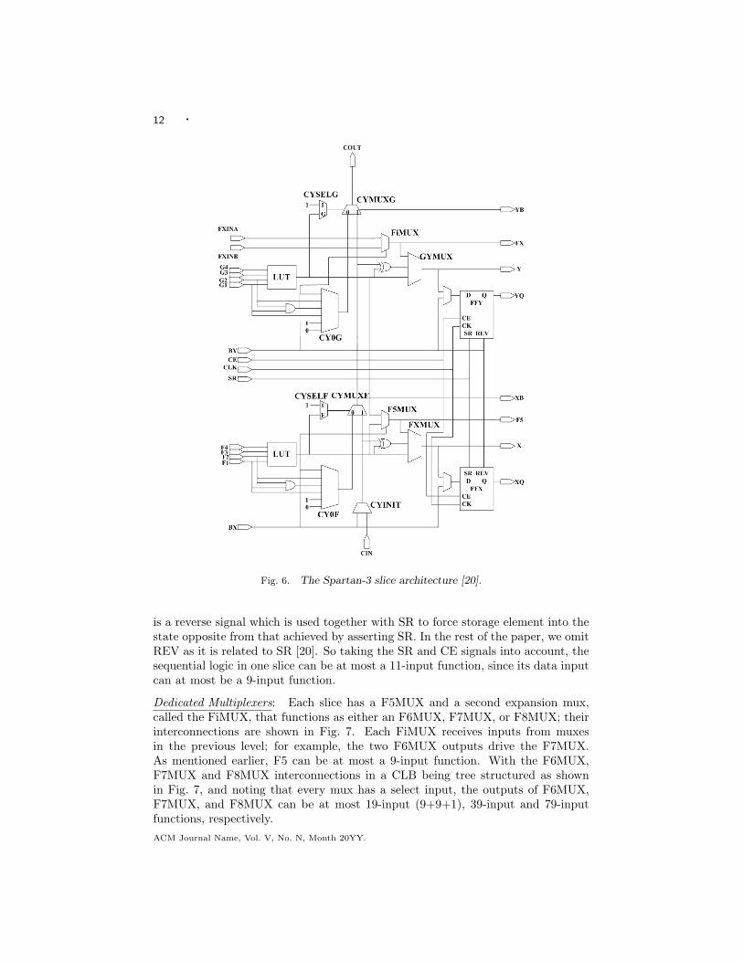
We briefly cover relevant features of the CLB architecture of the Xilinx Spartan-3 family FPGAs for which we have instantiated our trust design and checkingtechniques. The CLB architectural features of another popular family of XilinxFPGAs, the Virtex 4, are similar, and our trust design and checking techniquesare easily extendible to it. An FPGA is an m × n array of CLBs. The CLBs canbe programmed to implement combinational or sequential logic functions. All theCLBs are identical before they are configured. There are also input/output blocks(IOBs) and routing channels to provide interface between the package pins and theinternal circuit. Each CLB comprises four interconnected slices as shown in Fig. 5.All four slices have the following elements: two logic function generators or lookuptables (LUTs), two storage elements, wide-function multiplexers, and carry logic asshown in Fig. 6.
A slice has 16 inputs and 9 outputs. All the inputs/outputs are externally acces-sible except inputs CIN, FXINA, FXINB and F5 (shown in Fig. 6) which can beaccessed only internally within the CLB. We define an input/output as externallyaccessible (EA) if it can be connected to a routing channel (via a switch matrix).
Combinational Logic Functions: As we can see from Fig. 6, a LUT has four inputs,and thus can implement at most a 4-input function. Moreover, if we drive theoutputs of the two LUTs to the 2:1 multiplexer (mux) F5MUX, then, also countingits select input, its output F5 (which is non-EA) will be at most a 9-input function.If needed, F5 can be transmitted via another 2:1 mux FXMUX to its EA output Xin order to access external routing.
Sequential Logic Functions: The output of some combinational logic componentsin a slice drives the D-input of storage elements whose outputs are thus sequential.As we can see from Fig. 6, the storage element has four more inputs signals: CK,CE, SR, REV. CK is the clock input signal; CE is the clock enable signal. SR isa Set/Reset signal (its function is determined by a configuration bit): when SR isasserted, the storage element is Set or Reset depending on its configuration. REV
ACM Journal Name, Vol. V, No. N, Month 20YY.
12 ·
Fig. 6. The Spartan-3 slice architecture [20].
is a reverse signal which is used together with SR to force storage element into thestate opposite from that achieved by asserting SR. In the rest of the paper, we omitREV as it is related to SR [20]. So taking the SR and CE signals into account, thesequential logic in one slice can be at most a 11-input function, since its data inputcan at most be a 9-input function.
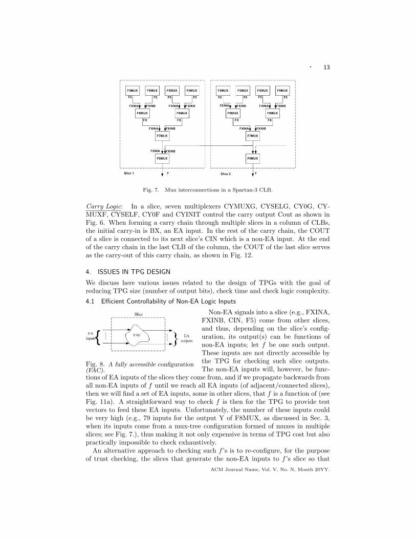
Dedicated Multiplexers: Each slice has a F5MUX and a second expansion mux,called the FiMUX, that functions as either an F6MUX, F7MUX, or F8MUX; theirinterconnections are shown in Fig. 7. Each FiMUX receives inputs from muxesin the previous level; for example, the two F6MUX outputs drive the F7MUX.As mentioned earlier, F5 can be at most a 9-input function. With the F6MUX,F7MUX and F8MUX interconnections in a CLB being tree structured as shownin Fig. 7, and noting that every mux has a select input, the outputs of F6MUX,F7MUX, and F8MUX can be at most 19-input (9+9+1), 39-input and 79-inputfunctions, respectively.ACM Journal Name, Vol. V, No. N, Month 20YY.
· 13
Fig. 7. Mux interconnections in a Spartan-3 CLB.
Carry Logic: In a slice, seven multiplexers CYMUXG, CYSELG, CY0G, CY-MUXF, CYSELF, CY0F and CYINIT control the carry output Cout as shown inFig. 6. When forming a carry chain through multiple slices in a column of CLBs,the initial carry-in is BX, an EA input. In the rest of the carry chain, the COUTof a slice is connected to its next slice’s CIN which is a non-EA input. At the endof the carry chain in the last CLB of the column, the COUT of the last slice servesas the carry-out of this carry chain, as shown in Fig. 12.
4. ISSUES IN TPG DESIGN
We discuss here various issues related to the design of TPGs with the goal ofreducing TPG size (number of output bits), check time and check logic complexity.
4.1 Efficient Controllability of Non-EA Logic Inputs
Non-EA signals into a slice (e.g., FXINA,
Fig. 8. A fully accessible configuration(FAC).
FXINB, CIN, F5) come from other slices,and thus, depending on the slice’s config-uration, its output(s) can be functions ofnon-EA inputs; let f be one such output.These inputs are not directly accessible bythe TPG for checking such slice outputs.The non-EA inputs will, however, be func-
tions of EA inputs of the slices they come from, and if we propagate backwards fromall non-EA inputs of f until we reach all EA inputs (of adjacent/connected slices),then we will find a set of EA inputs, some in other slices, that f is a function of (seeFig. 11a). A straightforward way to check f is then for the TPG to provide testvectors to feed these EA inputs. Unfortunately, the number of these inputs couldbe very high (e.g., 79 inputs for the output Y of F8MUX, as discussed in Sec. 3,when its inputs come from a mux-tree configuration formed of muxes in multipleslices; see Fig. 7.), thus making it not only expensive in terms of TPG cost but alsopractically impossible to check exhaustively.
An alternative approach to checking such f ’s is to re-configure, for the purposeof trust checking, the slices that generate the non-EA inputs to f ’s slice so that
ACM Journal Name, Vol. V, No. N, Month 20YY.

14 ·
the non-EA inputs are functions of very few EA inputs of their slices; see theconceptual depiction of this approach in Fig. 11b. This makes f a function of afew EA inputs in the locally re-configured FPGA, making it much less expensiveand practical to check f ; note that f ’s slice is not re-configured, and the checkingprocess can thus verify the correctness of the configuration of f ’s slice, which is thepurpose of the trust checking of f . Since f will be a function of not too many EAinputs for the purpose of checking, the check logic will also be a function of onlya few inputs. Thus this local-reconfiguration based approach for slice outputs withnon-EA inputs reduces both TPG and check logic cost, and also makes exhaustivechecking (generation of all input vectors to check a circuit slice output) practical.Further details of this approach are given below.
We define uncuttable rout-
Fig. 9. (a) Original configuration. (b) Simplified con-figuration for trust checking.
ings as routings from outputsof a slice to non-EA inputs ofanother slice in the same ordifferent CLB; see Fig. 11. Dueto the presence of inaccessibleinputs of a slice, we divide theconfiguration of a slice into threeparts for the purpose of effi-cient trust checking:(1) Fully accessible configura-tion (FAC) is a configuration(logic function) which has allEA inputs (Fig. 8).(2) Partially accessible config-uration (PAC) is a configura-tion for which some inputs arenon-EA inputs (Fig. 11(a)).
(3) Uncuttable routings.In Fig. 11(a), the PAC has non-EA inputs Y1, . . . , Ym and EA inputs Z1, . . . , Zk.
We can see that the non-EA inputs Y1, . . . , Ym of the PAC in Slice 2 are connectedto the outputs of the FAC in Slice 1 through uncuttable routings. Thus Y1, . . . , Ym
are functions of the FAC’s inputs X1, . . . , Xn. Thus to check this PAC in a straight-forward, though expensive, manner, we will require n + k TPG outputs to drivethese EA inputs. This is generally much larger than would be required if we haddirect access to the m non-EA inputs (in which case we would require m + k TPGbits), since in most cases n � m. In Step B of the TPG connection determinationalgorithm, R&T, given in Fig. 10, we give an approach to reduce the required TPGoutputs (test vector size) for checking PACs.
Example of Step B.1 of Algorithm R&T (Fig. 10): Consider the checking of theF6MUX which is a PAC. As we can see from Fig. 9(a), the F6MUX with outputY has non-EA inputs FXINA and FXINB that are connected to two F5 outputs,which are outputs of F5MUXes. As we mentioned in Sec. 3, F5 can be a functionof at most 9 EA inputs (see Fig. 9(a)). Thus Y can be a function of at most19 EA inputs, which means that we need a 19-bit TPG in order to check Y viaACM Journal Name, Vol. V, No. N, Month 20YY.

· 15
Algorithm Reconfigure & Test (R&T)
/* R&T determines the inputs that a TPG needs to drive for each slice output f beingchecked, and tests f accordingly. */
for each slice output f do
if f is the output of a FAC thenStep A: Test the FAC using the test vectors for f that directly feed the FAC’s inputs
as shown in Fig. 8.else /* f is the output of a PAC */
Step B:
(1) Determine the configuration of the FACs driving the PAC’s non-EA inputs so thatthe FAC’s outputs are either 0-input (i.e., the zero or one functions) or single-inputfunctions, so that each non-EA input is a function of as few EA inputs as possible. The
test vectors for f are the resulting set of EA inputs of f (some of these EA inputs areinputs to f ’s PAC, while the others are inputs to the reconfigured FACs feeding f ’snon-EA inputs)./* The original and changed configuration of the FAC(s) driving the non-EA inputs toachieve this are conceptually shown in Figs. 11(a) and (b). */
(2) Replace the original driving FACs’ configurations with the above determined FAC
configurations in the containing CLB’s configuration and load in the PG containing thecurrent PAC and its re-configured driving FACs (simultaneously do likewise for all PACsin the PG).
/* Note that this is easily done in the non-integrated embedding scenario (Sec. 7), whichneeds to be used if the circuit has PACs */
(3) Test the PAC using the above determined test vectors for f . These test vectors alsocheck the uncuttable routings feeding the PAC(s).
(4) Restore the above FACs to their original configuration.
/* This is automatically done when the circuit is restored after trust checking; see thenon-integrated embedding discussion in Sec. 7. */
endfor
End R&T.
Fig. 10. Algorithm for determining CLB configuration for testing PGs with FACs and/or PACs.
Note that this requires that the PACs and their driving FACs (that need to be reconfigured)cannot be in the same PG, as they cannot be tested together. Our PG determination step takes
care of this constraint.
Fig. 11. (a) Original FAC→ PAC configuration and uncuttable routings. (b) Test-efficientFAC → PAC configuration.
ACM Journal Name, Vol. V, No. N, Month 20YY.

16 ·
all its EA inputs. Furthermore, the parity check function of the parity group towhich Y belongs will be complex (at least a 19-input function). However, as shownFig. 9(b), for trust checking, we can reconfigure the LUTs feeding the F5MUXes sothat LUT 1 generates 0 and LUT 2 generates 1 (both 0-input functions). For sucha configuration, F5 = BX (the select input of each F5MUX) and hence F5 will bea function of only one input. As a result, Y will be a function of just 3 EA inputs(the two feeding F5MUX’s select inputs BX’s and the F6MUX’s own select inputBY). We thus decrease the number of test vector bits needed to check Y from 19to 3. Note that the original configurations of LUT 1 and LUT 2 are FACs and arechecked in a separate FPGA configuration in which the original configurations ofLUT 1 and LUT 2 are maintained, and the output of F5MUX is driven to its EAoutput.
4.2 Determining TPG Size
We define two slice outputs X and Y to be independent if no other slice outputdepends on both X and Y .
Lemma 4.1. Suppose O1 and O2 are independent slice outputs and O1 = f(p1,p2, p3, . . . , pm), O2 = g(q1, q2, q3, . . . , qn). When connecting TPG outputs to (p1,p2, p3, . . . , pm) and (q1, q2, q3, . . . , qn) (here, all these inputs are EA inputs), wecan share min(m,n) TPG outputs among the inputs of O1 and O2 and still be ableto check both outputs exhaustively.
Proof. Two inputs of independent outputs can share a TPG output because, inspite of the sharing, all combinations of their input vectors can be generated. This,however, does not hold if O1 and O2 are dependent outputs, since the output, sayO3, that depends on O1 and O2 cannot be checked by all combinations of inputvectors if there is sharing of even a single input between O1 and O2—if xi and yj
are the inputs of O1 and O2 that are driven by the same TPG output, then theonly input vectors for checking O3 will be those in which xi = yj (note that xi, yj
are also inputs of O3).The argument for sharing a TPG output among independent outputs extends to
min(m,n) TPG bits for min(m,n) inputs of O1, O2.
We perform exhaustive checking of each CLB output, and thus the TPG is asimple counter; we define the size T of the TPG as the number of counter bits. Twill be the larger of T1 and T2, where T1 is the TPG size determined in Step Aand T2 is the TPG size determined in Step B of algorithm R&T (Sec. 4.1). As wementioned in Sec. 3, the combinational output corresponding to a FAC will be afunction of at most 9 inputs, and a sequential logic output will depend on 11 inputsat most. So T1 is at most 11. We determine T2, the TPG size required to checkPACs as follows. As we discussed in the example for Step B of algorithm R&T,the output of F6MUX can be made to depend on only three inputs during checking.Using the same approach as for checking F6MUX and referring to Fig. 7, an outputof F7MUX can be made to depend on seven inputs (3+3+1), and similarly theoutput of F8MUX can be made a function of 15 inputs. Also, as we can see inFig. 12, the carry logic takes an EA input BX of Slice 1 as a carry-in and COUTof Slice N as the carry-out of this carry chain. Through reconfiguring the FAC andACM Journal Name, Vol. V, No. N, Month 20YY.

· 17
Fig. 12. Illustration of a simplified configuration associated with checking the carry-chainlogic.
PAC in the carry chain, each COUT in it can be made equal to the input CIN.Thus the final COUT of the carry chain can be made dependent on just one EAinput, BX. The above cover all non-EA inputs; thus T2 is at most 15, and the upperbound for T is also 15.
If we can determine a slice output fmax in the application circuit that is a functionof the largest number of inputs (either as a FAC or a PAC with reconfigured FACsfeeding it as described in algorithm R&T), then we can determine the exact size ofthe TPG required as the number of these inputs (≤ 15 from the above analysis).This is because, fmax has to be independent of all the other outputs. Suppose thisis not the case. Then there must be another output g which depends on fmax andat least one other slice output, so the input size of g must be larger than the inputsize of fmax, which contradicts our assumption that fmax is a function of the largestnumber of inputs. Thus since all other slice outputs are independent w.r.t. fmax,by Lemma 4.1, the inputs of any of these functions can share TPG outputs withfmax’s inputs (if they are in the same PG).
5. PARITY GROUP PATTERNS AND THEIR CHECK FUNCTIONS
Based on the number k of EA slice inputs that a slice output Oi depends on (eitherwhen Oi’s logic is a FAC or a PAC with local reconfiguration of feeding FACs asdescribed in Algorithm R&T), and its logic configuration structure, we categorizefour parity group patterns (PGPs). Each parity group is then formed with sliceoutputs of the same PGP in order to minimize the complexity of the correspondingcheck function. Here we discuss the check function complexity for parity groupsbelonging to each PGP for the case of even parity functions. We will later extendthese to random parity functions (see Sec. 6).
5.1 PGP 1: Combinational logic functions with k ≤ 4
The first PGP is characterized by combinational outputs of no more than fourinputs. Suppose there are t outputs O1, O2, . . . , Ot, all of them are independent,the number of their inputs is at most four and they are outputs of combinationallogic. According to Lemma 4.1, the TPG size needs to be at most four so as to feedthe inputs of all the Oi’s in order to check them simultaneously as outputs in thesame parity group. The check slice output function Oc will be
Oc = O1 ⊕O2 ⊕ . . .⊕Ot
and thus Oc will also be a function of no more than four inputs (note again thatduring checking, the inputs of each Oi are fed by the same test vectors; see Fig. 3a).Since a LUT can implement any function of four inputs, for a parity group belongingto PGP 1, we just need one LUT to implement the check function of all t outputs.
ACM Journal Name, Vol. V, No. N, Month 20YY.

18 ·
5.2 PGP 2: Sequential logic functions with k ≤ 6
PGP 2 is characterized by outputs of storage elements whose data input (D input)is a combinational logic function of at most four inputs; see Fig. 13.
The sequential logic may have two more
Fig. 13. Check slice configuration for aPGP 2 output.
input signals SR and CE. The combinationallogic part of a PGP-2 output is the datainput to its storage element which may beconfigured as a flip-flop or a latch. We ob-tain the XOR of all the combinational logicparts of PGP-2 outputs to determine thecombinational logic part of their check func-
tion. Then, as shown in Fig. 13, we connect this combinational parity check functionto the data input of a storage element to form the final sequential parity check func-tion of the PGP-2 outputs. Thus, we need just one LUT and one storage elementfor a PGP-2 parity check function.
We term the outputs of storage elements as SE outputs and the outputs of anycombinational logic as non-SE outputs. For an SE output Oi, we denote the com-binational logic function input to its storage element as comb(Oi), as shown in seeFig. 13. In an SE output, besides the combinational logic data input, there aretwo more inputs that affect the output, SR and CE that were introduced in Sec. 3.For an SE output, there are thus four different sequential (SE) configurations: (1)It has both SR and CE; (2) It has SR only; (3) It has CE only; (4) It has neitherSR nor CE. If the storage element does not have SR or CE inputs, it means thatthe storage element will not be Set/Reset or that the clock is always enabled. It sohappens that SE outputs with different SE configurations cannot be parity-checkedsimultaneously, as we prove below.
Lemma 5.1. : Two SE outputs that have different SE configurations cannot beparity-checked simultaneously, i.e., they cannot belong to the same parity group.
Proof. Here, we only prove that an SE output with SR (configuration 1 or2) cannot be checked together with an SE output without SR (configuration 3 or4); the other combinations’ incompatibility proofs are similar. Suppose there aretwo SE outputs O1 and O2, O1 has SR while O2 does not; hence O2 = comb(O2)always. Without loss of generality, let us assume that SR is configured as a SETsignal and O1 and O2 are the only two elements in a parity group. We denote thecheck slice’s output as Oc, and its combinational data input comb(Oc) is configuredas the function comb(O1)⊕ comb(O2). We have two cases:Case 1: The check slice’s configuration does not have SR. When SR is unassertedfor O1, O1 = comb(O1) and since O2 = comb(O2) and Oc = comb(Oc), we haveOc = O1⊕O2. However, when SR is asserted for O1, we have O1⊕O2 = 1⊕O2 = O2
while Oc remains = O1 ⊕O2. So Oc is not always the parity of O1 and O2.Case 2: The check slice’s configuration has SR. When SR is asserted for O1, O1 ⊕O2 = 1⊕ O2 = O2, while when SR is asserted for Oc, Oc = 1. Thus again Oc willnot be the parity of O1 and O2 unless O2 is always 0.
Thus irrespective of what the SE configuration of the check slice is, it will not beable to check O1 and O2 simultaneously.ACM Journal Name, Vol. V, No. N, Month 20YY.

· 19
The above lemma implies that SE outputs with different SE configurations willneed to be partitioned into different parity groups, which will increase the totalcheck function cost. However, this requirement can be circumvented by configuringin, during the trust checking phase, SR and/or CE signals to those SE outputs whichdo not have them as inputs. This enables us to check all of them in one parity group,and in only one check slice configuration, as established in the theorem below.
Theorem 5.1. : Let G2i be any set of PGP 2 outputs. Irrespective of whether
these outputs have SR/CE signals as their inputs or not, during the trust checkingprocess, we can configure them with SR and CE inputs, and we can implement theirparity check function in one slice configuration that also has SR and CE, so thatall outputs in G2
i can be included in one parity group and checked simultaneously.
Proof. Let O1, . . . , Om be the outputs in G2i . We design the combinational logic
part comb(Oc) of their check function Oc as comb(Oc) = comb(O1)⊕. . .⊕comb(Om).By controlling the SR and CE signals of each Oj by two TPG outputs (sharedacross all Oj ’s), and varying these signals to obtain the four SR/CE combinationsdescribed earlier, we check each Oj once in its original SR/CE configuration. Fur-thermore, for each SR/CE configuration, it can be shown that for the tamper-freecase, Oc = O1 ⊕ . . .⊕Om, and we thus obtain correct parity checking of G2
i .
5.3 PGP 3: Shannon’s expansion functions with 4 ≤ k ≤ 11
As we mentioned in Sec. 3, when driving two LUTs’ outputs to F5MUX, we canget at most a 9-input function at the output of F5MUX. We term the output ofF5MUX as an “intermediate” output fv. It can serve as a D-input to the storageelement in the slice and thus become an SE output XQ (which can be at mostan 11-input function if it has SR and CE inputs), or it can bypass the storageelement and be a non-SE output X, as shown in Fig. 14. fv can be represented asa Shannon’s expansion expression: fv = I · f() + I · g() where I is the mux’s selectsignal, and f and g are the functions implemented by the two LUTs driving thedata inputs of F5MUX. Outputs that fall into PGP 3 are those that are directlydriven by fv (X in Fig. 14) or the output of storage element driven by fv (XQ inFig. 14). Consider s such intermediate outputs of F5MUXes:
O1 = I · f1(x1, x2 . . . xm1) + I · g1(y1, y2 . . . yn1)O2 = I · f2(x1, x2 . . . xm2) + I · g2(y1, y2 . . . yn2)
...Os = I · fs(x1, x2 . . . xms
) + I · gs(y1, y2 . . . yns)
where 0 ≤ mi ≤ 4, 0 ≤ ni ≤ 4, mi+ni+1 > 4, ∀ i, 1 ≤ i ≤ s.The parity check function Oc of these intermediate outputs is:
Oc = O1 ⊕O2 . . .⊕Os.
We prove the following result about the structure of Oc.
Theorem 5.2. The parity check function Oc of PGP-3 intermediate outputsO1, . . . , Os has the following structure:
Oc = O1 ⊕O2 . . .⊕Os
ACM Journal Name, Vol. V, No. N, Month 20YY.

20 ·
= I · (f1 ⊕ f2 ⊕ . . .⊕ fs) + I · (g1 ⊕ g2 ⊕ . . .⊕ gs).
Proof. We prove this by induction on s.Induction Basis : We prove the theorem statement for s = 2.
Oc = O1 ⊕O2 = (If1 + Ig1)⊕ (If2 + Ig2)
= (If1 + Ig1) · (If2 + Ig2) + (If1 + Ig1) · (If2 + Ig2)= (If1 + Ig1) · (I + f2) · (I + g2) + (I + f1) · (I + g1) · (If2 + Ig2)
= (If1 + Ig1) · ((If2 + I g2) + ((If1 + I g1) · (If2 + Ig2)= If1f2 + Ig1g2 + If1f2 + I g1g2 = I(f1f2 + f1f2) + I(g1g2 + g1g2)
= I(f1 ⊕ f2) + I(g1 ⊕ g2).
Induction Hypothesis: The theorem statement is true for s = k.Induction Step: We need to show that given the basis and hypothesis, the theoremstatement is true for s = k + 1.
Oc = O1 ⊕O2 . . .⊕Ok+1 = (O1 ⊕O2 . . .⊕Ok)⊕Ok+1 ( since ⊕ is associative)= [I · (f1 ⊕ f2 ⊕ . . .⊕ fk) + I · (g1 ⊕ g2 ⊕ . . .⊕ gk)]⊕ [I · fk+1 + I · gk+1]
( from the induction hypothesis )= (I · f1,k + I · g1,k)⊕ (I · fk+1 + I · gk+1)
= where f1,k = f1 ⊕ f2 ⊕ . . .⊕ fk, and g1,k = g1 ⊕ g2 ⊕ . . .⊕ gk
= I · (f1,k ⊕ fk+1) + I · (g1,k ⊕ gk+1) ( from the induction basis )= I · (f1 ⊕ f2 ⊕ . . .⊕ fk ⊕ fk+1) + I · (g1 ⊕ g2 ⊕ . . .⊕ gk ⊕ gk+1).
It follows from the above theorem that
Oc = I · fc(x1, x2 . . . xm) + I · gc(y1, y2 . . . yn), 0 ≤ m ≤ 4, 0 ≤ n ≤ 4
where fc = f1⊕f2⊕ . . .⊕fs, and gc = g1⊕g2⊕ . . .⊕gs. Thus Oc also has the sameShannon’s expansion function structure as the Oi’s, and can thus be configured injust one slice as the F5MUX output with the mux’s inputs driven by its two LUTsthat implement fc and gc (similar to the configuration shown in Fig. 14).
Unlike PGP 1 and PGP 2, we will not check a set of PGP-3 SE outputs and non-SE outputs separately (in two separate parity groups), because that will requiretwo check slices. Our technique for checking PGP-3 outputs is as follows.
(1) During the trust checking process, change, if necessary (i.e., if the originalconfiguration is not the following desired configuration), the configuration of eachPGP-3 output so that both X and XQ are available at the corresponding sliceoutputs as shown in Fig. 14 (the original output of the slice could have been onlyX, only XQ or both).
(2) We configure the check slice in the same manner so that we can check the Xand XQ outputs corresponding to each Oi simultaneously (i.e., in one parity groupand in one check configuration). Thus the fv of the check slice is configured as theXOR function of all the fv’s in the parity group as derived above. Since the fv’sdrive the X outputs directly, the X output of the check slice is the parity functionof the X outputs in the parity group.ACM Journal Name, Vol. V, No. N, Month 20YY.

· 21
Fig. 14. Check slice configuration for PGP 3 outputs X and XQ.
(3) For the corresponding SE outputs XQ, their data inputs are the correspond-ing fv’s, and similar to PGP 2 outputs, and as spelled out in the proof of Theo-rem 5.1, during the trust-checking phase, SR and CE signals are added to thoseXQ’s which do not have them, and also to the check slice’s XQ output. Thus byTheorem 5.1, the XQ output of the check slice is always the parity of all the XQ’sin the PGP-3 parity group for each of the four combinations of SR and CE values.
We are thus able to check both SE outputs and non-SE outputs of this paritygroup simultaneously. Note that we may check more X and XQ outputs than thereare in the original circuit, but we check all the original X and XQ outputs as well.
5.4 PGP 4: Complex output functions with k > 4
There can be very complex functions of more than four inputs that do not fitinto PGP-3 categorization. For example, the output of F8MUX can be a 15-inputfunction during trust checking with local reconfiguration (as described in Sec. 4),and while the output of the corresponding parity check function of such functionswill be a 15-input function as well, it may not be implementable in a single slice.Unlike the PGP-3 case, the function structure may not be preserved when XOR’ingsuch 15-input functions. It is thus not possible to determine the configurationrequired to implement parity check functions analytically as we have done for PGPs1 to 3. We need to use synthesis tools to determine the implementation of theseparity check functions, and their implementation may require one or more slices.
6. TACKLING TPG/ORA TAMPERING VIA RANDOM PARITY POLARITIES
Our discussion so far assumed that the TPG and ORA are tamper-free. However, ifan adversary is able to obtain the TPG/ORA designs, he/she can tamper with themso that the actual circuit tampers go undetected. For example, a simple tamper ofan ORA in which its output is changed to implement the zero function will leadto all parities being detected as even in spite of the presence of circuit tampersand the resulting erroneous slice outputs. Similarly, the TPG can be tamperedto skip exactly those test vectors which exercise tampers inserted in the circuitCLBs, thus not detecting them. The TPG and ORA may also be tampered by thedevice programming unit during the loading of their configuration bits for trustchecking. We present here a technique using random parity vectors that ensuresvery high probability detection of design tampers even in the presence of tampersin the checking circuit (TPG and/or ORA).
ACM Journal Name, Vol. V, No. N, Month 20YY.
22 ·
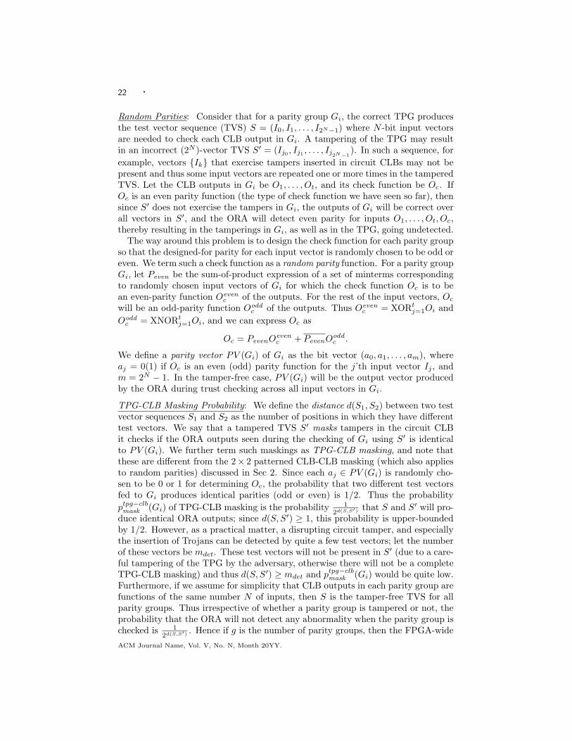
Random Parities: Consider that for a parity group Gi, the correct TPG producesthe test vector sequence (TVS) S = (I0, I1, . . . , I2N−1) where N -bit input vectorsare needed to check each CLB output in Gi. A tampering of the TPG may resultin an incorrect (2N )-vector TVS S′ = (Ij0 , Ij1 , . . . , Ij2N−1
). In such a sequence, forexample, vectors {Ik} that exercise tampers inserted in circuit CLBs may not bepresent and thus some input vectors are repeated one or more times in the tamperedTVS. Let the CLB outputs in Gi be O1, . . . , Ot, and its check function be Oc. IfOc is an even parity function (the type of check function we have seen so far), thensince S′ does not exercise the tampers in Gi, the outputs of Gi will be correct overall vectors in S′, and the ORA will detect even parity for inputs O1, . . . , Ot, Oc,thereby resulting in the tamperings in Gi, as well as in the TPG, going undetected.
The way around this problem is to design the check function for each parity groupso that the designed-for parity for each input vector is randomly chosen to be odd oreven. We term such a check function as a random parity function. For a parity groupGi, let Peven be the sum-of-product expression of a set of minterms correspondingto randomly chosen input vectors of Gi for which the check function Oc is to bean even-parity function Oeven
c of the outputs. For the rest of the input vectors, Oc
will be an odd-parity function Ooddc of the outputs. Thus Oeven
c = XORtj=1Oi and
Ooddc = XNORt
j=1Oi, and we can express Oc as
Oc = PevenOevenc + PevenOodd
c .
We define a parity vector PV (Gi) of Gi as the bit vector (a0, a1, . . . , am), whereaj = 0(1) if Oc is an even (odd) parity function for the j’th input vector Ij , andm = 2N − 1. In the tamper-free case, PV (Gi) will be the output vector producedby the ORA during trust checking across all input vectors in Gi.
TPG-CLB Masking Probability: We define the distance d(S1, S2) between two testvector sequences S1 and S2 as the number of positions in which they have differenttest vectors. We say that a tampered TVS S′ masks tampers in the circuit CLBit checks if the ORA outputs seen during the checking of Gi using S′ is identicalto PV (Gi). We further term such maskings as TPG-CLB masking, and note thatthese are different from the 2× 2 patterned CLB-CLB masking (which also appliesto random parities) discussed in Sec 2. Since each aj ∈ PV (Gi) is randomly cho-sen to be 0 or 1 for determining Oc, the probability that two different test vectorsfed to Gi produces identical parities (odd or even) is 1/2. Thus the probabilityptpg−clbmask (Gi) of TPG-CLB masking is the probability 1
2d(S,S′) that S and S′ will pro-duce identical ORA outputs; since d(S, S′) ≥ 1, this probability is upper-boundedby 1/2. However, as a practical matter, a disrupting circuit tamper, and especiallythe insertion of Trojans can be detected by quite a few test vectors; let the numberof these vectors be mdet. These test vectors will not be present in S′ (due to a care-ful tampering of the TPG by the adversary, otherwise there will not be a completeTPG-CLB masking) and thus d(S, S′) ≥ mdet and ptpg−clb
mask (Gi) would be quite low.Furthermore, if we assume for simplicity that CLB outputs in each parity group arefunctions of the same number N of inputs, then S is the tamper-free TVS for allparity groups. Thus irrespective of whether a parity group is tampered or not, theprobability that the ORA will not detect any abnormality when the parity group ischecked is 1
2d(S,S′) . Hence if g is the number of parity groups, then the FPGA-wide
ACM Journal Name, Vol. V, No. N, Month 20YY.

· 23
TPG-CLB tamper masking probability ptpg−clbmask is the probability that for each Gi,
the ORA’s output is the same as the expected parity vector PV (Gi). Thus, giventhat the random parity vectors are chosen independently for each parity group, wehave
ptpg−clbmask =
g∏i=1
ptpg−clbmask (Gi) =
12g·d(S,S′)
≤ 12g
.
In a medium-size FPGA such as the Spartan-3, as discussed in Sec. 2, there willbe in general four 50× 48 2D codes mapped to the CLB-output array, where each2D code has 50 + 48 + 2 = 100 parity groups; thus g = 400 and ptpg−clb
mask ≤ 12400 , an
extremely miniscule value.
ORA-CLB Masking Probability: For a correct TVS S, we denote the output vectorsequence of a parity group Gi by OV Si = (OV0, · · · , OV2N−1), where OVj is theoutput corresponding to test vector Ij . If a tamper in the CLB logic correspondingto output function Ok ∈ Gi produces an incorrect output for test vector Ir, thenOVr will have an incorrect parity that will be detected by a tamper-free ORA. Wedesign the ORA as a tree of 4-bit XOR functions, where each XOR is implementedby a 4-bit LUT. When some LUTs are tampered, and one of the tampers is exer-cised by the incorrect output vector OVr, then the ORA produces a reverse paritycompared to the one it should produce for the incorrect OVr, and thus the errorin OVr goes undetected; we term such a masking of the underlying tamper in theCLB logic that resulted in an incorrect OVr as ORA-CLB masking. Irrespectiveof how the tampers are distributed in the ORA and the CLBs of the parity groupGi, we can capture their effect by two parameters x < 1 and y < 1, where x is thefraction of ORA inputs that exercise the tamper(s) in the ORA so that an incorrectORA output is produced, and y is the fraction of output vectors in OV Si that areerroneous with an odd number of errors (and hence detectable by a correct ORA)5.The probability pora−clb
mask (Gi) of masking a tampered parity group by a tamperedORA = the probability of a tampered ORA not producing any incorrect output forany output vector of a tampered parity group Gi = (prob. that all odd-erroneousoutput vectors in OV Si exercise ORA tamper(s)) × (prob. that no other outputvectors in OV Si exercise any ORA tamper). Thus
pora−clbmask (Gi) = xy·2N
× (1− x)(1−y)2N
(3)
Obtaining the partial differentiations of Eqn. 3 w.r.t. x and y, equating them to0 and solving yields x = 1/2 and y = 1/2 for maximizing pora−clb
mask (Gi). Thus wehave,
pora−clbmask (Gi) ≤
122N
Once again, since all g parity groups are independently checked and have inde-pendently determined random parities, the masking probability for an entire trust-
5Note that even though an even number of errors are not detectable within a single parity group,each of these errors will also be present in other parity groups and will be detected, save for the2× 2 pattern of errors whose probability pmask we analyzed in Sec. 2.
ACM Journal Name, Vol. V, No. N, Month 20YY.

24 ·
checking phase is:
pora−clbmask ≤ 1
2g(2N )
For g = 400 and N = 4, this is a negligible probability.
Check-CLB Overhead for Random Parities: We note that random parity checkfunctions can be implemented in exactly the same CLB resources as even paritycheck functions for PGPs 1 to 3, the most common PGPs; we show this for PGP3. Recall that each PGP-3 output Oj is given by (see Sec. 5.3):
Oj = I · fj(x1, x2 . . . x4) + I · gj(y1, y2 . . . y4).
We proved in Sec. 5 that even parity PGP-3 check functions are also Shannonexpansion functions, and thus can also be implemented in a single slice, yieldinga low-complexity check function; the same holds true for odd-parity functions. Inorder to maintain this property for a random parity check function Oc for a PGP-3parity group G3
i we work backwards from the requirement that Oc should have aShannon expansion structure; thus we desire that Oc has the structure:
Oc = I · fc(x1, x2, x3, x4) + I · gc(y1, y2, y3, y4)
Suppose that G3i has t slice outputs O1, O2, · · · , Ot with each Oj given as above.
We generate two random 16-bit parity vectors PV f (G3i ) and PV g(G3
i ). Similarto the above definition of Peven, we define here P f
even as the SOP of mintermscorresponding to input vector Ir iff ar = 0, ar ∈ PV f (G3
i ); P geven is similarly
defined corresponding to PV g(G3i ). Next we define Of,even
c , Of,oddc , Og,even
c , Og,oddc :
Of,evenc = XORt
j=1fj , Of,oddc = XNORt
j=1fj
Og,evenc = XORt
j=1gj , Og,oddc = XNORt
j=1gj ,
We finally determine the check function Oc as:
Oc = I · (P feven ·Of,even
c + P feven ·Of,odd
c ) + I · (P geven ·Og,even
c + P geven ·Og,odd
c )= I · fc + I · gc
where fc = P feven ·Of,even
c + P feven ·Of,odd
c and gc = P geven ·Og,even
c + P geven ·Og,odd
c .It is easy to see that when I = 1, the output parity corresponding to input vector
Ir is determined by ar ∈ PV f (G3i ) (if ar = 0, P f
even = 1 and Oc = Of,evenc , the
even parity function, else Oc = Of,oddc , the odd parity function). A similar analysis
holds for I = 0. Thus the parities determined by Oc are random, since they arebased on random PVs PV f (G3
i ) and PV g(G3i ).
Finally, since in the above expression for Oc, each subexpression AND’ed with Iand I is a 4-input function, Oc for a random-parity PGP-3 group is also a Shannon’sexpansion function implementable in one slice with two LUTs and one Mux drivenby them (just as for the Oc’s for an even-parity PGP-3 group).
Our trust design flow that uses the various concepts developed in this paper isgiven in Fig. 15.ACM Journal Name, Vol. V, No. N, Month 20YY.

· 25
Fig. 15. Our ECC-based trust design flow. Steps 1 and 2 comprise the conventionaldesign flow, and the actual trust design flow begins from Step 3. It is assumed that theconventional design flow produces a correct design that is then used by the trust designflow to insert trust structures for detection of tampers that may be inserted after thetrust design flow is completed (e.g., at any point in the system integration pathway, atthe user’s end, or by remote attacks using high energy radiation such as electromagneticpulses that can flip on-chip configuration bits).
7. EMBEDDING CHECK COMPONENTS IN THE FPGA
We discuss here issues in the embedding of check components (check logic, TPG andORA) in the FPGA for the trust-checking phase, and the corresponding hardwareoverheads. There are two ways to embed check components into an FPGA circuit.One is integrated embedding, the other is non-integrated embedding.
Integrated Embedding: In this approach, we embed the check components into theunused CLBs in the FPGA along with the application circuit. During each paritygroup checking iteration, we just need to choose the corresponding check compo-nents and configure the required routing to connect the TPG to the inputs of thecircuit and check CLBs of the parity group to be checked, and the outputs of theseCLBs to the ORA. The check components in this scenario will impose a hardwareoverhead, and may minimally affect the timing of the original circuit. The advan-tage, however, of this type of embedding is the minimization of configuration timesince only the new routings need to be configured for each parity group checking.An example of integrated embedding is shown in Fig. 2b. Our trust design flow
ACM Journal Name, Vol. V, No. N, Month 20YY.

26 ·
Fig. 16. (a) A 4 × 4 CLB Array. (b) Non-integrated embedding based checking: a columnparity group being checked after configuring in the check components in adjoining regions;for simplicity we show a non-randomized parity group.
given earlier (Fig. 15) is for the non-integrated embedding scenario, though it iseasily modified for integrated embedding.
Non-Integrated Embedding: In this scenario, the check CLBs, TPG and ORA arenot integrated with the original circuit, but configured in when needed during thetrust-checking phase (Fig. 4). During this phase, the secret key sent to the userafter the trust-design phase (see Fig. 15) is used to extract each PG from the designconfiguration bits of the circuit that reaches the user, and check it for the presenceof design tampers as described earlier. One parity group is checked at a time, andeach time we embed the corresponding check components in other parity groups’space which are not being checked. In this way, our hardware overhead is 0% asfor each parity group checking, we actually reuse the hardware that are not beingchecked. Similarly, since the check circuit components are not present during thenormal circuit functioning, its performance is unaffected by this approach. Fig. 16shows a non-integrated checking of a parity group column (for simplicity, we showhere a non-randomized PG) of a 4 × 4 CLB array with the TPG, ORA and checkCLB configured in nearby positions. A screen shot of the check circuit and arandomized PG being checked (labeled as PGP3) is given in Fig. 17. Our trustdesign and checking flows given earlier (in Figs. 15 and 4, respectively) are for non-integrated embedding. After the checking phase, the original FPGA circuit (thatincludes non-functional CLBs configured with the logic zero function) is restoredin the FPGA, and normal circuit operation resumes.
ORA and Check Slice Overheads:Consider an FPGA with N CLBs. Irrespective of the size of the two dimensions
of the FPGA array, we can map a “logical” square m × m CLB array onto theactual FPGA array, where (m − 1)2 < N ≤ m2. For simplicity of exposition, wethus assume in the overhead analysis here that the FPGA has an m × m CLBarray; we thus also assume that an m×m 2D code is (randomly) embedded in it.As shown in Fig. 6, each slice has seven EA outputs, and so each CLB has 28 EAoutputs. Thus, in the embedded 2D code’s (random) CLB row/column, there are28m outputs. These outputs will fall into different PGPs. We assume that theseACM Journal Name, Vol. V, No. N, Month 20YY.

· 27
Fig. 17. Xilinx NCD screenshot of PG checking using non-integrated embedding.
outputs are on the average evenly distributed across the four PGPs available in eachrow/column of the embedded 2D code, so that each parity group corresponding toeach such PGP will have 7m outputs on the average.
The hardware cost of the ORA of size p (number of inputs = p) is an XOR-gatetree (a parity detector). Each LUT can implement a 4-input XOR function andeach slice has 2 LUTs. Thus the slice-cost of ORA of size p is:
ORAcost(p) = (p
4+
p
16+ . . . + 1)/2 ≈ p
6(4)
If the ORA size is p, then each potential parity group of size X will need to bedivided into dX
p e parity subgroups and be separately checked; each subgroup willhave its own parity check function (i.e., each such subgroup is a finally-determinedbonafide parity group). So the average check slice cost for each row/column of theembedded 2D code is
∑4j=1d
7mp e·Lj , where the summation is over the four different
types of parity groups, and Lj is the number of slices required to implement theparity function of PGP j. Thus the total hardware cost of check slices is:
CScost(p) = 2m×4∑
j=1
d7m
pe · Lj (5)
where 2m is the number of rows and columns of the embedded 2D code. Hence theoverall hardware cost A(p) we want to minimize is:
A(p) = ORAcost(p) + CScost(p). (6)
From Sec. 5, we know that L1 = L2 = 0.5 and L3 = 1 and we assume herethat L4 = 2 on the average. To minimize the hardware overhead, we equate the
ACM Journal Name, Vol. V, No. N, Month 20YY.

28 ·
Table I. Hardware overhead for a 64-bit TC.
CLB Slice
TPG (9-bit counter) 4 10
ORA 7 26
Check CLB/slice 24 94
64-bit TC circuit 34 75
Total FPGA size checked 480 1920
Hardware overhead 7.292% 6.771%
Table II. Hardware overhead for ICC.
CLB Slice
TPG (11-bit counter) 5 12
ORA 7 26
Check CLB/slice 24 95
ICC circuit 45 132
Total FPGA size checked 480 1920
Hardware overhead 7.500% 6.927%
Table III. Hardware overhead for RISC.
CLB Slice
TPG (15-bit counter) 9 28
ORA 2 6
Check CLB/slice 36 139
RISC proc. 290 1003
Total FPGA size checked 480 1920
Hardware overhead 9.792% 9.010%
differentiation of Eqn. 6 w.r.t. p to zero (with the simplifying assumption that d 7mp e
= 7mp ). We thereby get the ORA size (# of inputs) for the minimum overhead as
4√
21m ≈ 19m, and the minimum hardware overhead of check slices and ORA as4√
21m3 ≈ 7m slices. We assume that the average TPG (across all circuits) is an
11-bit counter (note that its maximum possible size is 15) which uses 12 slices. So
the total hardware overhead percentage will be4√
21m3 +12
4m2 × 100%.The FPGA we used in this experiment is the Spartan-3 XC3S200 FPGA which
has a 24 × 20 CLB array. We map a 22 × 22 CLB array onto it, thus m = 22.From the above expressions, the minimized hardware overhead percentage will onan average be 7.56% across different circuit implementations on the FPGA; this isborne out by our experimental results (see Tables I-III).
8. EXPERIMENTAL RESULTS
Using the two trust-design methodologies based on even and random parity groupswith an underlying 2D ECC developed in this paper, we check three circuits:I2C Controller Core (ICC) [11] (size of 45 CLBs, 132 slices), a 64-bit Tree Comparator(TC) (size of 24 CLBs, 75 slices), and a simple RISC processor risc16f84 [4] (size of290 CLBs, 1003 slices). Both the trust-design (Fig. 15) and trust-checking (Fig. 4)flows were manually followed, and ISE tools were used where indicated. We ob-ACM Journal Name, Vol. V, No. N, Month 20YY.

· 29
tained experimental data for the following metrics.
(a) Hardware overhead (includes TPG, check slice and ORA overheads) for the inte-grated embedding scenario (for non-integrated embedding the hardware overheadis 0).
(b) Tamper detection probability PD, defined as the % of time inserted tampersin the circuit or unused slices (extraneous logic) are detected in their respectiveparity group checking, and when TPG/ORA tampers are detected during paritygroup checking as unexpected ORA outputs.
(c) False alarm probability PFA is the % of time the checking of a tamper-freeparity group results in an unexpected ORA output when the TPG and ORA arealso tamper free.
(d) Detection latency (DL) of the parity group checking process, defined as thenumber of test vectors fed across tampered parity groups before the first tamperis correctly detected.
(e) Circuit time overhead, which is the increase in the critical path delay of thecircuit in the integrated embedding scenario (for non-integrated embedding thecircuit time overhead is 0).
Hardware Overhead: As explained in Sec. 7, for non-integrated embedding, thehardware overhead is 0%. Using integrated embedding, the hardware (CLB) over-head of the three circuits are 7.5% for ICC and 7.3% for TC, and 9.8% for RISC,as we can see from Tables I-III.
Fault-Detection and False-Alarm Probabilities: We insert 3 types of CLB tampers:(i) Logic Function Tamper (LFT): tamper of only the combinational logic; (ii)Storage Element-related Tamper (SET): tamper of the sequential elements of aCLB; (iii) Interconnection Tamper (IT): tamper of internal interconnections withina CLB. We insert one to ten tampers into the circuit CLBs in the following pro-portion: 60% LFT, 30% SET and 10% IT. We also insert TPG and ORA tampers:we insert one to three tampers each into the TPG and ORA (half of them are LFTand the other half IT).
The average PD and PFA results for the three circuits are shown in Tables IV-V;each PD and PFA is calculated based on 20 different tamper injection experiments.While we check all parity groups of the two medium-size circuits, for efficiency,we insert tampers in and check a few randomly chosen parity groups of the RISCcircuit; statistically, the PD and PFA results obtained for RISC are representativeof the PD and PFA that would be obtained if all its parity groups are checked.
As we can see from Table IV, for the even parity technique, all the PFA’s are0% which is very promising. Almost all the PD’s are 100% except for two cases:(1) During the experiment, we insert one to three tampers in the TPG circuit 20times when there are no tampers in the circuit CLBs. The PD obtained is 0%which indicates that TPG tampers cannot be detected when using the even paritytechnique. (2) We randomly insert stuck-at-0 tampers (among other tampers) atvarious CLB outputs of the ORA, including the final ORA output. The latter casewill always lead to a non-detection of circuit tampers for the even-parity technique.Overall (over various random tampers of the ORA), in the ORA tampered and
ACM Journal Name, Vol. V, No. N, Month 20YY.

30 ·
Table IV. Average PD and PFA results across all circuits for the even-parity technique.
Logic tamper location TPG &ORA
tamperfree
TPGtampered
only
ORAtampered
only
TPG &ORA
tampered
a. Existing logic PD PFA PD PFA PD PFA PD PFA
0 tamper NA 0% 0% 0% 95% 0% 95% 0%
1-10 tampers 100% 0% 100% 0% 95% 0% 95% 0%
b. Extra logic
1-5 CLBs 100% 0% 100% 0% 95% 0% 95% 0%
Table V. Average PD and PFA results across all circuits for the random-parity technique.
Logic tamper location TPG &
ORAtamperfree
TPG
tamperedonly
ORA
tamperedonly
TPG &
ORAtampered
a. Existing logic PD PFA PD PFA PD PFA PD PFA
0 tamper NA 0% 100% 0% 100% 0% 100% 0%
1-10 tampers 100% 0% 100% 0% 100% 0% 100% 0%
b. Extra logic
1-5 CLBs 100% 0% 100% 0% 100% 0% 100% 0%
TPG & ORA tampered cases, the PD is 95%. As shown in Table V, in the randomparity technique, however, the PD’s are 100% for all cases, which underscores thesignificantly higher reliability for this technique, and its promise for FPGA trustdesign.
We also randomly insert extraneous logic in one to five empty CLBs in the fol-lowing PGP categories: 50% PGP 1, 30% PGP 2, and 20% PGP 3. Average resultsacross 10 such experiments are given in Tables IV and V; all the PD’s are 100%except the PD’s for the even-parity technique when the ORA is tampered, whilethe PFA’s are always 0%. This empirically establishes that our techniques can alsodetect extraneous logic with very high probability (as is also theoretically evidentfrom the discussion of our techniques) and without false alarms.Detection Latency: For the detection latency (DL) metric, for expediency we ob-tained results for both parity techniques for only the ICC circuit and with onetamper in it (either LFT, SET or IT). Once again, taking the TPG and ORA intoaccount, there are four different tamper configurations as tabulated in Tables VIand VII. As shown in Tables VI and VII, the DLs of the random parity techniqueare smaller than those of the even parity technique when the TPG is tampered,while the DLs of the two techniques are the same when both TPG and ORA aretamper free or only the ORA is tampered. The DLs of the random parity techniquewhen the TPG is tampered are all 2’s because each parity group has different pari-ties across their input vectors, and thus if the TPG is tampered, we are very likelyto detect the tamper quickly. Finally, the average DL of the even parity techniqueis 280 units while the average DL of the random parity technique is 169 units, a40% improvement.ACM Journal Name, Vol. V, No. N, Month 20YY.
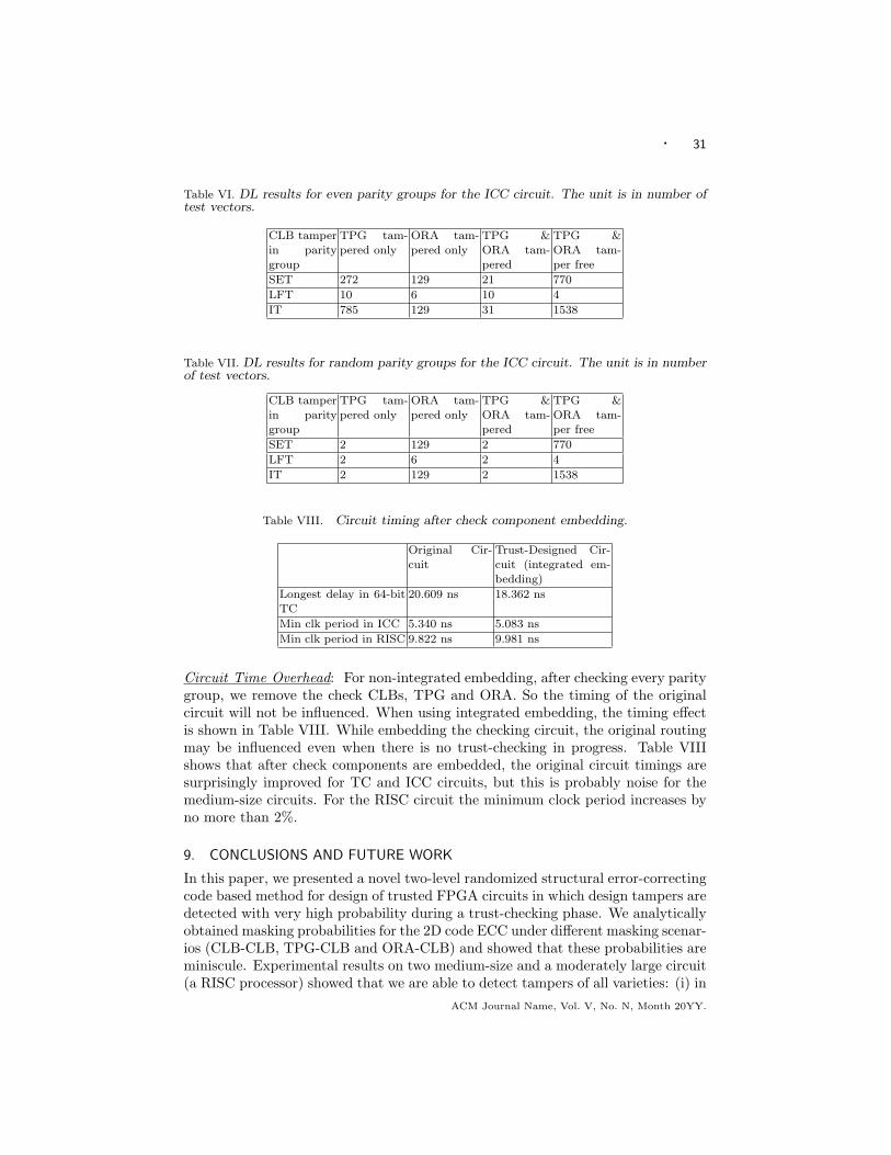
· 31
Table VI. DL results for even parity groups for the ICC circuit. The unit is in number oftest vectors.
CLB tamperin parity
group
TPG tam-
pered only
ORA tam-
pered only
TPG &
ORA tam-pered
TPG &
ORA tam-per free
SET 272 129 21 770
LFT 10 6 10 4
IT 785 129 31 1538
Table VII. DL results for random parity groups for the ICC circuit. The unit is in numberof test vectors.
CLB tamper
in paritygroup
TPG tam-
pered only
ORA tam-
pered only
TPG &
ORA tam-pered
TPG &
ORA tam-per free
SET 2 129 2 770
LFT 2 6 2 4
IT 2 129 2 1538
Table VIII. Circuit timing after check component embedding.
Original Cir-
cuit
Trust-Designed Cir-
cuit (integrated em-bedding)
Longest delay in 64-bit
TC
20.609 ns 18.362 ns
Min clk period in ICC 5.340 ns 5.083 ns
Min clk period in RISC 9.822 ns 9.981 ns
Circuit Time Overhead: For non-integrated embedding, after checking every paritygroup, we remove the check CLBs, TPG and ORA. So the timing of the originalcircuit will not be influenced. When using integrated embedding, the timing effectis shown in Table VIII. While embedding the checking circuit, the original routingmay be influenced even when there is no trust-checking in progress. Table VIIIshows that after check components are embedded, the original circuit timings aresurprisingly improved for TC and ICC circuits, but this is probably noise for themedium-size circuits. For the RISC circuit the minimum clock period increases byno more than 2%.
9. CONCLUSIONS AND FUTURE WORK
In this paper, we presented a novel two-level randomized structural error-correctingcode based method for design of trusted FPGA circuits in which design tampers aredetected with very high probability during a trust-checking phase. We analyticallyobtained masking probabilities for the 2D code ECC under different masking scenar-ios (CLB-CLB, TPG-CLB and ORA-CLB) and showed that these probabilities areminiscule. Experimental results on two medium-size and a moderately large circuit(a RISC processor) showed that we are able to detect tampers of all varieties: (i) in
ACM Journal Name, Vol. V, No. N, Month 20YY.

32 ·
circuit CLBs—LUT functions, storage elements, and internal interconnections; (ii)in the checker circuit comprising the TPG and ORA; (iii) insertions of extraneouslogic. With a small hardware overhead, we achieved a tamper detection probabilityof 100% and a false alarm probability of 0% for the random-parity technique.
We have recently developed routing-tamper checking as a significant extensionto the CLB/slice checking techniques discussed here; this will be addressed in afuture paper. In future work, we will develop techniques to detect IP tampering.An approach for this is to use the IP’s output functions, which are known (e.g.,for an FFT IP, it is known what functions of the inputs each output is) to derivecheck logic for these functions and those of other (IP or non-IP) CLB outputsthat are placed in the same parity group. Another topic for future investigationis determining the reliability-to-cost tradeoffs offered by different ECCs such as3-D, full-2, full-3 and Hamming codes. These ECCs and tradeoffs can be part ofa trust-design toolset that automatically chooses the ECC that best matches theuser-provided reliability and cost numbers.
Acknowledgements
We thank the associate editors and the anonymous referees for their comments,which have helped improve this paper. This work was made possible in part byNSF grants CCR-0204097 and CCF-0811855.
REFERENCES
[1] ADELL, P., AND Allen, G. 2008. Assessing and Mitigating Radiation Effects in XilinxFPGAs. JPL Publication 08-9, 2/08.
[2] BOLCHINI, C., QUARTA, D., AND SANTAMBROGIO, M. D. 2007. SEU Mitigation for
SRAM-Based FPGAs through Dynamic Partial Reconfiguration. Proceedings of the 17th ACM
Great Lakes symposium on VLSI, Stresa-Lago Maggiore, Italy, 2007, ACM, New York, NY,55-60.
[3] CARMICHAEL, C., CAFFREY, M., AND SALAZAR, A. 2000. Correcting Single EventUpsets through Virtex Partial Configuration. Xilinx Application Note XAPP 216.
Available at http://www.xilinx.com/support/documentation/application notes/xapp216.pdf.
[4] CLAYTON, J. risc16f84: Overview.Available at http://www.opencores.org/projects.cgi/web/risc16f84/overview.
[5] DARPA Trusted IC program webpage:
http://www.darpa.mil/mto/solicitations/baa07-24/index.html.
[6] DIPERT, B. Cunning circuits confound crooks.Available at http://www.e-insite.net/ednmag/contents/images/21df2.pdf.
[7] DUTT, S., MAHAPATRA, N.R. 1997. Node-Covering, Error-Correcting Codes and Multi-processors with Very High Average Fault Tolerance. IEEE Trans. Computers 46(9), 997-1015.
[8] DYER, J., LINDEMANN, M., PEREZ, R., SAILER, R., SMITH S.W., VAN DOORN,
L., AND WEINGART, S. 2001. Building the IBM 4758 Secure Coprocessor. IEEE Computer,
Volume 34, Issue 10, 57-66.
[9] GIBSON, G.A., HELLERSTEIN, L., KARP, R.M., KATZ, R.H., AND PATTERSON, D.A.
1989. Failure correction techniques for large disk arrays. Third Int’l Conf. on ArchitecturalSupport for Programming Languages and Operating Systems (ASPLOS), Boston, MA, April
1989, ACM, New York, NY, 123-132.
ACM Journal Name, Vol. V, No. N, Month 20YY.

· 33
[10] HEINER, J., COLLINS, N., AND Wirthlin, M. 2008. Fault Tolerant ICAP Controller
for High-Reliable Internal Scrubbing, IEEE Aerospace Conference, Big Sky, MT, March 2008,1-10.
[11] HERVEILLE, R. Available at http://www.opencores.org/projects.cgi/web/i2c/overview.
[12] KOCHER, P., JAFFE, J., AND JUN, B. 1999. Differential Power Analysis. Advances inCryptology (CRYPTO ’99), M. Wiener, Ed. Vol. LNCS 1666, Springer-Verlag, 388-397.
[13] KOMMERLING, O. AND KUHN, M. 1999. Design Principles for Tamper-Resistant Smart-card Processors. USENIX Workshop on Smartcard Technology (Smartcard ’99), Chicago, May1999, 9-20.
[14] SAXENA, N.R., FRANCO, P., AND MCCLUSKEY, E.J. 1992. Simple bounds on serial
signature analysis aliasing for random testing, Special Issue on Fault Tolerant Computing. IEEETrans. Computers, Volume 41, No. 5, 638-645.
[15] STEINER, N.J. 2002. A Standalone Wire Database for Routing and Tracing in XilinxVirtex, Virtex-E, and Virtex-II FPGAs. Master Thesis of Electrical Engineering, Virginia
Polytechnic Institute and State University, August 30, 2002.
[16] TRIMBERGER, S. 2007. Trusted Design in FPGAs, Proc. Design Automation Conference
(DAC), San Diego, CA, 2007, ACM, New York, NY, 5-8.
[17] WEINGART, S.H. Physical Security Devices for Computer Subsystems: A Survey ofAttacks and Defenses, Workshop on Cryptographic Hardware and Embedded Systems, 2000.
[18] WOLLINGER, T., GUAJARDO, J., AND PAAR, C., Cryptography on FPGAs: State of
the Art Implementations and Attacks. Special Issue on Embedded Systems and Security of theACM Trans. in Embedded Computing Systems (TECS), March 2003.
[19] WOLLINGER, T., AND PAAR, C. 2003. How Secure Are FPGAs in Cryptographic
Applications? Proc. Int’l Conf. Field Prog. Logic and Appl. (FPL), 2003, Springer-Verlag,
91-100.
[20] Xilinx Spartan-3 FPGA Family Complete Date Sheet.
Available at http://direct.xilinx.com/bvdocs/publications/ds099.pdf.
[21] Xilinx Virtex-4 User Guide.Available at http://www.xilinx.com/bvdocs/userguides/ug071.pdf.
[22] Xilinx Virtex-5 User Guide.Available at http://www.xilinx.com/bvdocs/userguides/ug191.pdf.
[23] Xilinx, Using Dedicated Multiplexers in Spartan-3 Generation FPGAs.
Available at http://www.xilinx.com/bvdocs/appnotes/xapp466.pdf.
[24] YANG, B., WU, K., AND KARRI, R. 2005. Secure Scan: A Design-for-Test Architecture
for Crypto Chips. Proc. Design Automation Conference (DAC), Anaheim, CA, June 2005,
ACM, New York, NY, 135-140.
ACM Journal Name, Vol. V, No. N, Month 20YY.