TPS65910,659101-109 - Texas Instruments · Product Folder Sample & Buy Technical Documents Tools &...
107
Product Folder Sample & Buy Technical Documents Tools & Software Support & Community TPS65910, TPS65910A, TPS65910A3, TPS659101 TPS659102, TPS659103, TPS659104, TPS659105 TPS659106, TPS659107, TPS659108, TPS659109 SWCS046U – MARCH 2010 – REVISED OCTOBER 2014 TPS65910x Integrated Power-Management Unit Top Specification 1 Device Overview 1.1 Features 1 • Embedded Power Controller • Two Enable Signals Multiplexed with SR-I 2 C, Configurable to Control any Supply State and • Two Efficient Step-Down DC-DC Converters for Processor Cores Supply Voltage Processor Cores • Thermal Shutdown Protection and Hot-Die • One Efficient Step-Down DC-DC Converter for I/O Detection Power • An RTC Resource With: • One Efficient Step-Up 5-V DC-DC Converter – Oscillator for 32.768-kHz Crystal or 32-kHz • SmartReflex™ Compliant Dynamic Voltage Built-in RC Oscillator Management for Processor Cores – Date, Time, and Calendar • 8 LDO Voltage Regulators and One Real-Time Clock (RTC) LDO (Internal Purpose) – Alarm Capability • One High-Speed I 2 C Interface for General-Purpose • One Configurable GPIO Control Commands (CTL-I 2 C) • DC-DC Switching Synchronization Through • One High-Speed I 2 C Interface for SmartReflex Internal or External 3-MHz Clock Class 3 Control and Command (SR-I 2 C) 1.2 Applications • Portable and Handheld Systems • Industrial Systems 1.3 Description The TPS65910 device is an integrated power-management IC available in 48-QFN package and dedicated to applications powered by one Li-Ion or Li-Ion polymer battery cell or 3-series Ni-MH cells, or by a 5-V input; it requires multiple power rails. The device provides three step-down converters, one step- up converter, and eight LDOs and is designed to support the specific power requirements of OMAP-based applications. Two of the step-down converters provide power for dual processor cores and are controllable by a dedicated class-3 SmartReflex interface for optimum power savings. The third converter provides power for the I/Os and memory in the system. The device includes eight general-purpose LDOs providing a wide range of voltage and current capabilities. The LDOs are fully controllable by the I 2 C interface. The use of the LDOs is flexible; they are intended to be used as follows: Two LDOs are designated to power the PLL and video DAC supply rails on the OMAP-based processors, four general-purpose auxiliary LDOs are available to provide power to other devices in the system, and two LDOs are provided to power DDR memory supplies in applications requiring these memories. In addition to the power resources, the device contains an embedded power controller (EPC) to manage the power sequencing requirements of the OMAP systems and an RTC. Table 1-1. Device Information (1) PART NUMBER PACKAGE (PIN) BODY SIZE TPS65910 PVQFN (48) 6.00 mm × 6.00 mm (1) For more information, see Section 8, Mechanical Packaging and Orderable Information. 1 An IMPORTANT NOTICE at the end of this data sheet addresses availability, warranty, changes, use in safety-critical applications, intellectual property matters and other important disclaimers. PRODUCTION DATA.
Transcript of TPS65910,659101-109 - Texas Instruments · Product Folder Sample & Buy Technical Documents Tools &...

Product
Folder
Sample &Buy
Technical
Documents
Tools &
Software
Support &Community
TPS65910, TPS65910A, TPS65910A3, TPS659101TPS659102, TPS659103, TPS659104, TPS659105
TPS659106, TPS659107, TPS659108, TPS659109SWCS046U –MARCH 2010–REVISED OCTOBER 2014
TPS65910x Integrated Power-Management Unit Top Specification1 Device Overview
1.1 Features1
• Embedded Power Controller • Two Enable Signals Multiplexed with SR-I2C,Configurable to Control any Supply State and• Two Efficient Step-Down DC-DC Converters forProcessor Cores Supply VoltageProcessor Cores
• Thermal Shutdown Protection and Hot-Die• One Efficient Step-Down DC-DC Converter for I/ODetectionPower
• An RTC Resource With:• One Efficient Step-Up 5-V DC-DC Converter– Oscillator for 32.768-kHz Crystal or 32-kHz• SmartReflex™ Compliant Dynamic Voltage
Built-in RC OscillatorManagement for Processor Cores– Date, Time, and Calendar• 8 LDO Voltage Regulators and One Real-Time
Clock (RTC) LDO (Internal Purpose) – Alarm Capability• One High-Speed I2C Interface for General-Purpose • One Configurable GPIO
Control Commands (CTL-I2C) • DC-DC Switching Synchronization Through• One High-Speed I2C Interface for SmartReflex Internal or External 3-MHz Clock
Class 3 Control and Command (SR-I2C)
1.2 Applications• Portable and Handheld Systems • Industrial Systems
1.3 DescriptionThe TPS65910 device is an integrated power-management IC available in 48-QFN package anddedicated to applications powered by one Li-Ion or Li-Ion polymer battery cell or 3-series Ni-MH cells, orby a 5-V input; it requires multiple power rails. The device provides three step-down converters, one step-up converter, and eight LDOs and is designed to support the specific power requirements of OMAP-basedapplications.
Two of the step-down converters provide power for dual processor cores and are controllable by adedicated class-3 SmartReflex interface for optimum power savings. The third converter provides powerfor the I/Os and memory in the system.
The device includes eight general-purpose LDOs providing a wide range of voltage and currentcapabilities. The LDOs are fully controllable by the I2C interface. The use of the LDOs is flexible; they areintended to be used as follows: Two LDOs are designated to power the PLL and video DAC supply railson the OMAP-based processors, four general-purpose auxiliary LDOs are available to provide power toother devices in the system, and two LDOs are provided to power DDR memory supplies in applicationsrequiring these memories.
In addition to the power resources, the device contains an embedded power controller (EPC) to managethe power sequencing requirements of the OMAP systems and an RTC.
Table 1-1. Device Information (1)
PART NUMBER PACKAGE (PIN) BODY SIZETPS65910 PVQFN (48) 6.00 mm × 6.00 mm
(1) For more information, see Section 8, Mechanical Packaging and Orderable Information.
1
An IMPORTANT NOTICE at the end of this data sheet addresses availability, warranty, changes, use in safety-critical applications,intellectual property matters and other important disclaimers. PRODUCTION DATA.

VFB1
INT1
PWRON
VREF
REFGND
Test interface
CLK32KOUT
VAUX33
VMMC
OSC32KIN
OSC32KOUT
TESTV
SLEEP
NRESPWRON
PWRHOLD
BOOT1BOOT0
SDASR_EN2
SCLSR_EN1
SDA_SDI
VDAC
VPLL
VAUX1
VRTC
Real-timeclock
VFB3
SW3
VDIG2
VAUX2
VDIG1
VDD1(SMPS)
VCC1
GND1
SW1
VFBIO
VBAT
VCC7
VCC7
VCC7
VBAT
VBAT
VBATVCC6
VCC3VCC4
VCC5
VCC 7
VBAT
VCC7
VDDIO
VDDIO
AGND2
AGND
AGND
GNDAGNDA
DGND
VAUX33
REFGND
GND3
OSC32-kHz
SCL_SCK
BuscontrolGPIO_CKSYNC
Powercontrolstate-
machine
Analogreferences
and comparators
VB
AC
KU
P
Backupmanagement
VRTC (LDO)and POR
VFB2
VCC2
GND2
SW2
VCCIO
GNDIO
SWIO
GN
DP
AGND
AGND2
AGND2
VDAC(LDO)
VPLL(LDO)
VAUX1(LDO)
VAUX2(LDO)
VDIG1(LDO)
AGND2
AGND2
AGND2
VDIG2(LDO)
VAUX33(LDO)
VMMC(LDO)
I C2
I C2
AGND2
AGND
AGND
VCC7
VCC7
VCC4
VDD2(SMPS)
VIO(SMPS)
VDD3(SMPS)
SWCS046-001
GNDP: Power pad ground
Ci(VCC7)
Co(VRTC)
Co(VREF)
Co(VDAC)
Ci(VCC5)
CBB
Co(VPLL)
Co(VAUX1)
Ci(VCC4)
Co(VAUX2)
DGND AGND AGND2 GND3Co(VMMC)
VBAT
Ci(VCC4)
Co(VAUX33)
Co(VDIG2)
Co(VDIG1)
Co(VIO)
Ci(VCCIO)
VBAT
Ci(VCC2)
Co(VDD2)
VBAT
Ci(VCC1)
Co(VDD1)
Co(VDD3)
Ci(VDD3)
TPS65910, TPS65910A, TPS65910A3, TPS659101TPS659102, TPS659103, TPS659104, TPS659105TPS659106, TPS659107, TPS659108, TPS659109SWCS046U –MARCH 2010–REVISED OCTOBER 2014 www.ti.com
1.4 Functional Block DiagramFigure 1-1 shows the top-level diagram of the device.
Figure 1-1. 48-QFN Top-Level Diagram
2 Device Overview Copyright © 2010–2014, Texas Instruments IncorporatedSubmit Documentation Feedback
Product Folder Links: TPS65910 TPS65910A TPS65910A3 TPS659101 TPS659102 TPS659103 TPS659104TPS659105 TPS659106 TPS659107 TPS659108 TPS659109

TPS65910, TPS65910A, TPS65910A3, TPS659101TPS659102, TPS659103, TPS659104, TPS659105
TPS659106, TPS659107, TPS659108, TPS659109www.ti.com SWCS046U –MARCH 2010–REVISED OCTOBER 2014
Table of Contents1 Device Overview ......................................... 1 5.20 VAUX1 and VAUX2 LDO ........................... 31
1.1 Features .............................................. 1 5.21 VDAC and VPLL LDO............................... 331.2 Applications........................................... 1 5.22 Timing and Switching Characteristics ............... 351.3 Description............................................ 1 6 Detailed Description ................................... 451.4 Functional Block Diagram ............................ 2 6.1 Power Reference.................................... 45
2 Revision History ......................................... 4 6.2 Power Sources ...................................... 453 Device Comparison ..................................... 6 6.3 Embedded Power Controller ........................ 454 Terminal Configuration and Functions.............. 7 6.4 32-kHz RTC Clock .................................. 52
4.1 Signal Descriptions ................................... 8 6.5 RTC ................................................. 535 Specifications ........................................... 10 6.6 Backup Battery Management ....................... 55
5.1 Absolute Maximum Ratings ......................... 10 6.7 Backup Registers ................................... 565.2 Handling Ratings .................................... 10 6.8 I2C Interface......................................... 565.3 Recommended Operating Conditions............... 11 6.9 Thermal Monitoring and Shutdown ................. 565.4 Thermal Resistance Characteristics for RSL 6.10 Interrupts ............................................ 57
Package ............................................. 13 6.11 Package Description ................................ 575.5 I/O Pullup and Pulldown Characteristics ............ 14 6.12 Functional Registers ................................ 585.6 Digital I/O Voltage Electrical Characteristics........ 15 7 Device and Documentation Support ............... 955.7 I2C Interface and Control Signals ................... 16 7.1 Device Support ...................................... 955.8 Power Consumption................................. 17 7.2 Documentation Support ............................. 965.9 Power References and Thresholds ................. 17 7.3 Related Links........................................ 965.10 Thermal Monitoring and Shutdown ................. 18 7.4 Community Resources .............................. 975.11 32-kHz RTC Clock .................................. 18 7.5 Trademarks.......................................... 975.12 Backup Battery Charger ............................ 19 7.6 Electrostatic Discharge Caution..................... 975.13 VRTC LDO .......................................... 19 7.7 Export Control Notice ............................... 975.14 VIO SMPS........................................... 20 7.8 Glossary ............................................. 975.15 VDD1 SMPS ........................................ 22 7.9 Additional Acronyms ................................ 985.16 VDD2 SMPS ........................................ 24 8 Mechanical Packaging and Orderable5.17 VDD3 SMPS ........................................ 26 Information .............................................. 995.18 VDIG1 and VDIG2 LDO............................. 27 8.1 Packaging Information .............................. 995.19 VAUX33 and VMMC LDO........................... 29
Copyright © 2010–2014, Texas Instruments Incorporated Table of Contents 3Submit Documentation Feedback
Product Folder Links: TPS65910 TPS65910A TPS65910A3 TPS659101 TPS659102 TPS659103 TPS659104TPS659105 TPS659106 TPS659107 TPS659108 TPS659109

TPS65910, TPS65910A, TPS65910A3, TPS659101TPS659102, TPS659103, TPS659104, TPS659105TPS659106, TPS659107, TPS659108, TPS659109SWCS046U –MARCH 2010–REVISED OCTOBER 2014 www.ti.com
2 Revision HistoryNOTE: Page numbers for previous revisions may differ from page numbers in the current version.VERSION DATE NOTES
* 03/2010 See (1)
A 05/2010 See (2)
B 06/2010 See (3)
C 06/2010 See (4)
D 11/2010 See (5)
E 01/2011 See (6)
F 01/2011 See (7)
G 05/2011 See (8)
H 06/2011 See (9)
I 07/2011 See (10)
J 10/2011 See (11)
K 10/2011 See (12)
L 01/2012 See (13)
M 03/2012 See (14)
N 04/2012 See (15)
O 06/2012 See (16)
P 09/2012 See (17)
Q 09/2012 See (18)
R 02/2013 See (19)
S 08/2013 See (20)
(1) Initial release(2) SWCS046A: Updated register tables VMMC_REG and VDAC_REG. Added register table VPLL_REG(3) SWCS046B: Updated Absolute Maximum Ratings, Recommended Operating Conditions, I/O Pullup and Pulldown Characteristics,
Digital I/Os Voltage Electrical Characteristics, Power Consumption, Power References and Thresholds, Thermal Monitoring andShutdown, 32-kHz RTC Clock, VRTC LDO, VIO SMPS, VDD1 SMPS, VDD2 SMPS, VDD3 SMPS, Switch-On/-Off Sequences andTiming
(4) SWCS046C: Associate parts; no change.(5) SWCS046D: Updated Recommended Operating Conditions - Backup Battery, I/O Pullup and Pulldown Characteristics, Backup Battery
Charger. Update Rated output current, PMOS current limit (High-Side), NMOS current limit (Low-Side), and Conversion Efficiency forVIO SMPS, VDD1/VDD2/VDD3 SMPS and VDIG1/VDIG2 LDO. Update Input Voltage for VIO/VDD1/VDD2 SMPS. Update DC andTransient Load and Line Regulation and Internal Resistance for VDIG1/VDIG2 LDO, VAUX33/VMMC LDO, VAUX1,VAUX2, LDO, andVDAC/VPLL LDO. Update DC Load Regulation for VAUX3/VMMC/VDAC. Update Power Control Timing. Add Device SLEEP StateControl. Add SMPS Switching Synchronization. Update VIO_REG, VDD1_REG, and VDD2_REG.
(6) SWCS046E: Manually added Thermal Pad Mechanical Data.(7) SWCS046F: UpdatedTable 3-1, SUPPORTED PROCESSORS AND CORRESPONDING PART NUMBERS.(8) SWCS046G: Updated Section 6.11, Section 5.3, Section 5.6, and Section 6.3.3.6.(9) SWCS046H: Updated Table 6-29, PUADEN_REG, Table 6-61, RESERVED, and Table 6-62, RESERVED.(10) SWCS046I: Updated DC Output voltage VOUT in Section 5.20.(11) SWCS046J: UpdatedTable 3-1, SUPPORTED PROCESSORS AND CORRESPONDING PART NUMBERS.(12) SWCS046K: UpdateTable 3-1, SUPPORTED PROCESSORS AND CORRESPONDING PART NUMBERS - Add AM335x.(13) SWCS046L: Updated Table 3-1, SUPPORTED PROCESSORS AND CORRESPONDING PART NUMBERS - Add AM335x with DDR2
and AM335x with DDR3.(14) SWCS046M: Updated Section 6.3.1, - Update Device Sleep enable conditions control information.(15) SWCS046N:
• Section 5.14 - Updated PMOS current limit (high side) conditions• Table 6-63 - Updated INT_STS_REG register - VMBHI_IT description• Updated Input voltage: Section 5.18
(16) SWCS046O: Updated Table 5-5, Power Control Timing Characteristics• Replace unit of µs for tdbPWRONF by ms
(17) SWCS046P: Updated Table 3-1, SUPPORTED PROCESSORS AND CORRESPONDING PART NUMBERS -• Add AM335x with DDR3 - TPS65910A31A1RSL• Add Rockchip - RK30xx
(18) SWCS046Q: Updated Table 3-1, SUPPORTED PROCESSORS AND CORRESPONDING PART NUMBERS -• Refer to SWCU093 document: Updated document reference from TBD to SWCU093
(19) SWCS046R: Updated Section 5.13, VRTC LDO - Changed Input Voltage - Back-up mode - Max from 3V to 5.5V.(20) SWCS046S: Updated Section 5.20, VAUX1 AND VAUX2 LDO - Changed VAUX2 - Rated Output Current IOUTmax - On mode from 150
mA to 300 mA
4 Revision History Copyright © 2010–2014, Texas Instruments IncorporatedSubmit Documentation Feedback
Product Folder Links: TPS65910 TPS65910A TPS65910A3 TPS659101 TPS659102 TPS659103 TPS659104TPS659105 TPS659106 TPS659107 TPS659108 TPS659109

TPS65910, TPS65910A, TPS65910A3, TPS659101TPS659102, TPS659103, TPS659104, TPS659105
TPS659106, TPS659107, TPS659108, TPS659109www.ti.com SWCS046U –MARCH 2010–REVISED OCTOBER 2014
VERSION DATE NOTEST 09/2013 See (21)
U 10/2014 See (22)
(21) SWCS046T: Updated• Table 6-23, RTC_Reset_Status_Reg, Changed Reserved bits to 7:1 and changed RESET_STATUS's reset value to 0x0.• Table 6-34, VDD1_OP_REG, Changed SEL Vout to Vout = (SEL[6:0] × 12.5 mV + 0.5625 V) × G.• Table 6-35, VDD1_SR_REG, Changed SEL Vout to Vout = (SEL[6:0] × 12.5 mV + 0.5625 V) × G.• Table 6-37, VDD2_OP_REG, Changed SEL Vout to Vout = (SEL[6:0] × 12.5 mV + 0.5625 V) × G.• Table 6-38, VDD2_SR_REG, Changed SEL Vout to Vout = (SEL[6:0] × 12.5 mV + 0.5625 V) × G.
(22) SWCS046U: Updated data sheet to latest TI standards• Updated Section 1.2, Applications• Added Table 1-1, Device Information• Moved Section 4, Terminal Configuration and Functions• Moved appropriate data to Section 5.2• Added Section 5.4, Thermal Resistance Characteristics for RSL Package
Copyright © 2010–2014, Texas Instruments Incorporated Revision History 5Submit Documentation Feedback
Product Folder Links: TPS65910 TPS65910A TPS65910A3 TPS659101 TPS659102 TPS659103 TPS659104TPS659105 TPS659106 TPS659107 TPS659108 TPS659109

TPS65910, TPS65910A, TPS65910A3, TPS659101TPS659102, TPS659103, TPS659104, TPS659105TPS659106, TPS659107, TPS659108, TPS659109SWCS046U –MARCH 2010–REVISED OCTOBER 2014 www.ti.com
3 Device Comparison
Table 3-1. Supported Processors and Corresponding Part Numbers
Compatible Processor (1) Part Number (1)
TI processor - AM335x with DDR2 TPS65910AA1RSLTI processor - AM335x with DDR3 TPS65910A3A1RSL
TI processor - AM335x with DDR3 (2) TPS65910A31A1RSLTI processors - AM1705/07, AM1806/08, AM3505/17, AM3703/15, DM3730/25, TPS65910A1RSL
OMAP-L137/38, OMAP3503/15/25/30, TMS320C6742/6/8Samsung - S5PV210, S5PC110 TPS659101A1RSL
Rockchip - RK29xx, RK30xx TPS659102A1RSLSamsung - S5PC100 TPS659103A1RSLSamsung - S5P6440 TPS659104A1RSL
TI processors - DM643x, DM644x TPS659105A1RSLReserved TPS659106A1RSL
Freescale - i.MX27, Freescale - i.MX35 TPS659107A1RSLFreescale - i.MX508 TPS659108A1RSLFreescale - i.MX51 TPS659109A1RSL
(1) The RSL package is available in tape and reel. See for details for corresponding part numbers, quantities and ordering information.(2) Refer to SWCU093, TPS65910Ax User's Guide For AM335x Processors
6 Device Comparison Copyright © 2010–2014, Texas Instruments IncorporatedSubmit Documentation Feedback
Product Folder Links: TPS65910 TPS65910A TPS65910A3 TPS659101 TPS659102 TPS659103 TPS659104TPS659105 TPS659106 TPS659107 TPS659108 TPS659109

1 2 3 4 5 6 7 8 9
SLEEP 37
CLK32KOUT 38
GPIO/CKSYN 39
NRESPWRON 40
VCC2 41
SW2 42
GND2 43
VFB2 44
INT1 45
VAUX1 46
VCC4 47
VAUX2 48
24 VPLL
23 VCC5
22 VDAC
21 OSC32KOUT
20 OSC32KIN
19 BOOT1
18 VREF
17 REFGND
16 VFBIO
15 GNDIO
14 SWIO
13 VCCIO
PowerPad
VC
C1
SW
1
GN
D1
PW
RO
N
VF
B1
SW
3
VF
B3
VR
RT
C
VC
C7
VB
AC
KU
P
BO
OT
0
TE
ST
V
36
35
34
33
32
31
30
29
28
27
26
25
10
11
12
PW
RH
OLD
VM
MC
VC
C3
VA
UX
33
VD
IG2
VC
C6
VD
IG1
SD
A
SC
L
SD
AS
R/E
N2
SC
LS
R/E
N1
VD
DIO
SWCS046-004
TPS65910, TPS65910A, TPS65910A3, TPS659101TPS659102, TPS659103, TPS659104, TPS659105
TPS659106, TPS659107, TPS659108, TPS659109www.ti.com SWCS046U –MARCH 2010–REVISED OCTOBER 2014
4 Terminal Configuration and Functions
Figure 4-1 shows the pin assignments.
Figure 4-1. 48-QFN Top-View Pin Assignment
Copyright © 2010–2014, Texas Instruments Incorporated Terminal Configuration and Functions 7Submit Documentation Feedback
Product Folder Links: TPS65910 TPS65910A TPS65910A3 TPS659101 TPS659102 TPS659103 TPS659104TPS659105 TPS659106 TPS659107 TPS659108 TPS659109

TPS65910, TPS65910A, TPS65910A3, TPS659101TPS659102, TPS659103, TPS659104, TPS659105TPS659106, TPS659107, TPS659108, TPS659109SWCS046U –MARCH 2010–REVISED OCTOBER 2014 www.ti.com
4.1 Signal Descriptions
Table 4-1. Signal DescriptionsNAME QFN PIN SUPPLIES TYPE I/O DESCRIPTION PU/PD
VDDIO VDDIO/DGND Power I Digital I/Os supply NoI2C bidirectional data signal/serial
SDA_SDI VDDIO/DGND Digital I/O peripheral interface data input External PU(multiplexed)I2C bidirectional clock signal/serial
SCL_SCK VDDIO/DGND Digital I/O peripheral interface Clock Input External PU(multiplexed)I2C SmartReflex bidirectional dataSDASR_EN2 VDDIO/DGND Digital I/O External PUsignal/enable of supplies (multiplexed)I2C SmartReflex bidirectional clockSCLSR_EN1 VDDIO/DGND Digital I/O External PUsignal/enable of supplies (multiplexed)Active-sleep state transition control Programmable PDSLEEP VDDIO/DGND Digital I signal (default active)Configurable general-purpose I/O or Programmable PDGPIO_CKSYNC VDDIO/DGND Digital I/O DC-DCs synchronization clock input (default active)signal
Programmable PDPWRHOLD VRTC/DGND Digital I Switch-on/-off control signal (default active)Programmable PUPWRON VBAT/DGND Digital I External switch-on control (ON button) (default active)PD active duringNRESPWRON VDDIO/DGND Digital O Power off reset device OFF state
INT1 VDDIO/DGND Digital O Interrupt flag NoProgrammable PDBOOT0 VRTC/DGND Digital I Power-up sequence selection (default active)Programmable PDBOOT1 VRTC/DGND Digital I Power-up sequence selection (default active)
PD disable inCLK32KOUT VDDIO/DGND Digital O 32-kHz clock output ACTIVE or SLEEP
stateOSC32KIN VRTC/REFGND Analog I 32-kHz crystal oscillator NoOSC32KOUT VRTC/REFGND Analog I 32-kHz crystal oscillator NoVREF VCC7/REFGND Analog O Bandgap voltage NoREFGND REFGND Analog I/O Reference ground NoTESTV VCC7/AGND Analog O Analog test output (DFT) No
Backup battery input (short to VCC5 ifVBACKUP VBACKUP/AGND Power I Nonot used)VCC1 VCC1/GND1 Power I VDD1 DC-DC power input NoGND1 VCC1/GND1 Power I/O VDD1 DC-DC power ground NoSW1 VCC1/GND1 Power O VDD1 DC-DC switched output NoVFB1 VCC7/AGND Analog I VDD1 feedback voltage PDVCC2 VCC2/GND2 Power I VDD2 DC-DC power input NoGND2 VCC2/GND2 Power I/O VDD2 DC-DC power ground NoSW2 VCC2/GND2 Power O VDD2 DC-DC switched output NoVFB2 VCC4/AGND2 Analog I VDD2 DC-DC feedback voltage PDVCCIO VCCIO/GNDIO Power I VIO DC-DC power input NoGNDIO VCCIO/GNDIO Power I/O VIO DC-DC power ground NoSWIO VCCIO/GNDIO Power O VIO DC-DC switched output NoVFBIO VCC7/AGND Analog I VIO feedback voltage PDVCC3 VCC3/AGND2 Power I VMMC VAUX33 power input NoVMMC VCC3/REFGND Power O LDO regulator output PD
8 Terminal Configuration and Functions Copyright © 2010–2014, Texas Instruments IncorporatedSubmit Documentation Feedback
Product Folder Links: TPS65910 TPS65910A TPS65910A3 TPS659101 TPS659102 TPS659103 TPS659104TPS659105 TPS659106 TPS659107 TPS659108 TPS659109

TPS65910, TPS65910A, TPS65910A3, TPS659101TPS659102, TPS659103, TPS659104, TPS659105
TPS659106, TPS659107, TPS659108, TPS659109www.ti.com SWCS046U –MARCH 2010–REVISED OCTOBER 2014
Table 4-1. Signal Descriptions (continued)NAME QFN PIN SUPPLIES TYPE I/O DESCRIPTION PU/PD
LDO regulator output, VDD3 internalVAUX33 VCC3/REFGND Power O PDregulated supplyVCC4 VCC4/AGND2 Power I VAUX1, VAUX2 power input NoVAUX1 VCC4/REFGND Power O LDO regulator output PDVAUX2 VCC4/REFGND Power O LDO regulator output PDVCC5 VCC5/AGND Power I VDAC, VPLL power input NoVDAC VCC5/REFGND Power O LDO regulator output PDVPLL VCC5/REFGND Power O LDO regulator output PDVRTC VCC7/REFGND Power O LDO regulator output PDVCC6 VCC6/AGND2 Power I VDIG1, VDIG2 power input NoVDIG1 VCC6/REFGND Power O LDO regulator output NoVDIG2 VCC6/REFGND Power O LDO regulator output No
VRTC power input, VDD3 internal andVCC7 VCC7/REFGND Power I Noanalog references supplyVFB3 VCC7/AGND Analog I VDD3 feedback voltage NoSW3 VCC7/GND3 Power O VDD3 DC-DC switched output No
PowerGND3 AGND Power I/O VDD3 DC-DC power ground NoPADPowerAGND AGND Power I/O Analog ground NoPADPowerAGND2 AGND Power I/O Analog ground NoPADPowerDGND DGND Power I/O Digital ground NoPAD
Copyright © 2010–2014, Texas Instruments Incorporated Terminal Configuration and Functions 9Submit Documentation Feedback
Product Folder Links: TPS65910 TPS65910A TPS65910A3 TPS659101 TPS659102 TPS659103 TPS659104TPS659105 TPS659106 TPS659107 TPS659108 TPS659109

TPS65910, TPS65910A, TPS65910A3, TPS659101TPS659102, TPS659103, TPS659104, TPS659105TPS659106, TPS659107, TPS659108, TPS659109SWCS046U –MARCH 2010–REVISED OCTOBER 2014 www.ti.com
5 Specifications
5.1 Absolute Maximum Ratings (1) (2)
over operating free-air temperature range (unless otherwise noted)MIN MAX UNIT
Voltage range on pins/balls VCC1, VCC2, VCCIO, VCC3, VCC4, VCC5, VCC6, VCC7 –0.3 7 VVoltage range on pins/balls VDDIO –0.3 3.6 VVoltage range on pins/balls OSC32KIN, OSC32KOUT, BOOT1, BOOT0 –0.3 VRTCMAX + 0.3 VVoltage range on pins/balls SDA_SDI, SCL_SCK, SDASR_EN2, SCLSR_EN1, SLEEP, –0.3 VDDIOMAX + 0.3 VINT1, CLK32KOUT, NRESPWRONVoltage range on pins/balls PWRON –0.3 7 VVoltage range on pins/balls PWRHOLD (3) GPIO_CKSYNC (4) –0.3 7 VPeak output current on all other terminals than power resources –5 5 mA
(1) Stresses beyond those listed under absolute maximum ratings may cause permanent damage to the device. These are stress ratingsonly, and functional operation of the device at these or any other conditions beyond those indicated under recommended operatingconditions is not implied. Exposure to absolute-maximum-rated conditions for extended periods may affect device reliability.
(2) All voltage values are with respect to VSS, unless otherwise noted.(3) I/O supplied from VDDIO but which can be driven from to a VBAT voltage level(4) I/O supplied from VRTC but can be driven to a VBAT voltage level
5.2 Handling RatingsMIN MAX UNIT
Tstg Storage temperature range –45 150 °CHuman Body Model (HBM), per ANSI/ESDA/JEDEC –2 2 kVJS001 (1)Electrostatic discharge (ESD)VESD performance: Charged Device Model (CDM), All pins –500 500 Vper JESD22-C101 (2)
(1) JEDEC document JEP155 states that 500-V HBM allows safe manufacturing with a standard ESD control process.(2) JEDEC document JEP157 states that 250-V CDM allows safe manufacturing with a standard ESD control process.
10 Specifications Copyright © 2010–2014, Texas Instruments IncorporatedSubmit Documentation Feedback
Product Folder Links: TPS65910 TPS65910A TPS65910A3 TPS659101 TPS659102 TPS659103 TPS659104TPS659105 TPS659106 TPS659107 TPS659108 TPS659109

TPS65910, TPS65910A, TPS65910A3, TPS659101TPS659102, TPS659103, TPS659104, TPS659105
TPS659106, TPS659107, TPS659108, TPS659109www.ti.com SWCS046U –MARCH 2010–REVISED OCTOBER 2014
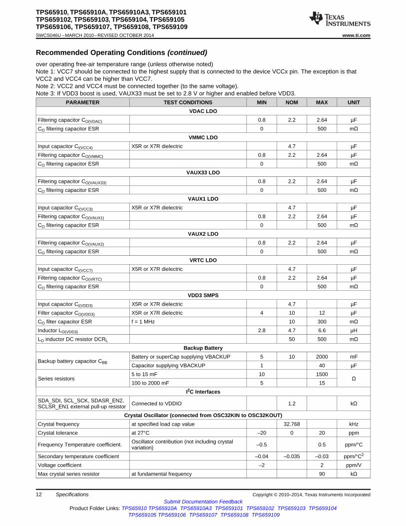
5.3 Recommended Operating Conditionsover operating free-air temperature range (unless otherwise noted)Note 1: VCC7 should be connected to the highest supply that is connected to the device VCCx pin. The exception is thatVCC2 and VCC4 can be higher than VCC7.Note 2: VCC2 and VCC4 must be connected together (to the same voltage).Note 3: If VDD3 boost is used, VAUX33 must be set to 2.8 V or higher and enabled before VDD3.
PARAMETER TEST CONDITIONS MIN NOM MAX UNITVCC: Input voltage range on pins/balls VCC1, VCC2, VCCIO, VCC3, VCC4, VCC5, 2.7 3.6 5.5 VVCC7VCCP: Input voltage range on pins/balls VCC6 1.7 3.6 5.5 VInput voltage range on pins/balls VDDIO 1.65 1.8/3.3 3.45 VInput voltage range on pins/balls PWRON 0 3.6 5.5 VInput voltage range on pins/balls SDA_SDI, SCL_SCK, SDASR_EN2, SCLSR_EN1, 1.65 VDDIO 3.45 VSLEEPInput voltage range on pins/balls PWRHOLD, GPIO_CKSYNC 1.65 VDDIO 5.5 VInput voltage range on balls BOOT1, BOOT0, OSC32KIN 1.65 VRTC 1.95 VOperating free-air temperature, TA –40 27 85 °CJunction temperature, TJ –40 27 125 °CStorage temperature range –65 27 150 °CLead temperature (soldering, 10 s) 260 °C
Power ReferencesVREF filtering capacitor CO(VREF) Connected from VREF to REFGND 100 nF
VDD1 SMPSInput capacitor CI(VCC1) X5R or X7R dielectric 10 µFFilter capacitor CO(VDD1) X5R or X7R dielectric 4 10 12 µFCO filter capacitor ESR f = 3 MHz 10 300 mΩInductor LO(VDD1) 2.2 µHLO inductor dc resistor DCRL 125 mΩ
VDD2 SMPSInput capacitor CI(VCC2) X5R or X7R dielectric 10 µFFilter capacitor CO(VDD2) X5R or X7R dielectric 4 10 12 µFCO filter capacitor ESR f = 3 MHz 10 300 mΩInductor LO(VDD2) 2.2 µHLO inductor dc resistor DCRL 125 mΩ
VIO SMPSInput capacitor CI(VIO) X5R or X7R dielectric 10 µFFilter capacitor CO(VIO) X5R or X7R dielectric 4 10 12 µFCO filter capacitor ESR f = 3 MHz 10 300 mΩInductor LO(VIO) 2.2 µHLO inductor dc resistor DCRL 125 mΩ
VDIG1 LDOInput capacitor CI(VCC6) X5R or X7R dielectric 4.7 µFFiltering capacitor CO(VDIG1) 0.8 2.2 2.64 µFCO filtering capacitor ESR 0 500 mΩ
VDIG2 LDOFiltering capacitor CO(VDIG2) 0.8 2.2 2.64 µFCO filtering capacitor ESR 0 500 mΩ
VPLL LDOInput capacitor CI(VCC5) X5R or X7R dielectric 4.7 µFFiltering capacitor CO(VPLL) 0.8 2.2 2.64 µFCO filtering capacitor ESR 0 500 mΩ
Copyright © 2010–2014, Texas Instruments Incorporated Specifications 11Submit Documentation Feedback
Product Folder Links: TPS65910 TPS65910A TPS65910A3 TPS659101 TPS659102 TPS659103 TPS659104TPS659105 TPS659106 TPS659107 TPS659108 TPS659109
TPS65910, TPS65910A, TPS65910A3, TPS659101TPS659102, TPS659103, TPS659104, TPS659105TPS659106, TPS659107, TPS659108, TPS659109SWCS046U –MARCH 2010–REVISED OCTOBER 2014 www.ti.com
Recommended Operating Conditions (continued)over operating free-air temperature range (unless otherwise noted)Note 1: VCC7 should be connected to the highest supply that is connected to the device VCCx pin. The exception is thatVCC2 and VCC4 can be higher than VCC7.Note 2: VCC2 and VCC4 must be connected together (to the same voltage).Note 3: If VDD3 boost is used, VAUX33 must be set to 2.8 V or higher and enabled before VDD3.
PARAMETER TEST CONDITIONS MIN NOM MAX UNITVDAC LDO
Filtering capacitor CO(VDAC) 0.8 2.2 2.64 µFCO filtering capacitor ESR 0 500 mΩ
VMMC LDOInput capacitor CI(VCC4) X5R or X7R dielectric 4.7 µFFiltering capacitor CO(VMMC) 0.8 2.2 2.64 µFCO filtering capacitor ESR 0 500 mΩ
VAUX33 LDOFiltering capacitor CO(VAUX33) 0.8 2.2 2.64 µFCO filtering capacitor ESR 0 500 mΩ
VAUX1 LDOInput capacitor CI(VCC3) X5R or X7R dielectric 4.7 µFFiltering capacitor CO(VAUX1) 0.8 2.2 2.64 µFCO filtering capacitor ESR 0 500 mΩ
VAUX2 LDOFiltering capacitor CO(VAUX2) 0.8 2.2 2.64 µFCO filtering capacitor ESR 0 500 mΩ
VRTC LDOInput capacitor CI(VCC7) X5R or X7R dielectric 4.7 µFFiltering capacitor CO(VRTC) 0.8 2.2 2.64 µFCO filtering capacitor ESR 0 500 mΩ
VDD3 SMPSInput capacitor CI(VDD3) X5R or X7R dielectric 4.7 µFFilter capacitor CO(VDD3) X5R or X7R dielectric 4 10 12 µFCO filter capacitor ESR f = 1 MHz 10 300 mΩInductor LO(VDD3) 2.8 4.7 6.6 µHLO inductor DC resistor DCRL 50 500 mΩ
Backup BatteryBattery or superCap supplying VBACKUP 5 10 2000 mF
Backup battery capacitor CBB Capacitor supplying VBACKUP 1 40 µF5 to 15 mF 10 1500
Series resistors Ω100 to 2000 mF 5 15
I2C InterfacesSDA_SDI, SCL_SCK, SDASR_EN2, Connected to VDDIO 1.2 kΩSCLSR_EN1 external pull-up resistor
Crystal Oscillator (connected from OSC32KIN to OSC32KOUT)Crystal frequency at specified load cap value 32.768 kHzCrystal tolerance at 27°C –20 0 20 ppm
Oscillator contribution (not including crystalFrequency Temperature coefficient. –0.5 0.5 ppm/°Cvariation)Secondary temperature coefficient –0.04 –0.035 –0.03 ppm/°C2
Voltage coefficient –2 2 ppm/VMax crystal series resistor at fundamental frequency 90 kΩ
12 Specifications Copyright © 2010–2014, Texas Instruments IncorporatedSubmit Documentation Feedback
Product Folder Links: TPS65910 TPS65910A TPS65910A3 TPS659101 TPS659102 TPS659103 TPS659104TPS659105 TPS659106 TPS659107 TPS659108 TPS659109

TPS65910, TPS65910A, TPS65910A3, TPS659101TPS659102, TPS659103, TPS659104, TPS659105
TPS659106, TPS659107, TPS659108, TPS659109www.ti.com SWCS046U –MARCH 2010–REVISED OCTOBER 2014
Recommended Operating Conditions (continued)over operating free-air temperature range (unless otherwise noted)Note 1: VCC7 should be connected to the highest supply that is connected to the device VCCx pin. The exception is thatVCC2 and VCC4 can be higher than VCC7.Note 2: VCC2 and VCC4 must be connected together (to the same voltage).Note 3: If VDD3 boost is used, VAUX33 must be set to 2.8 V or higher and enabled before VDD3.
PARAMETER TEST CONDITIONS MIN NOM MAX UNITCrystal load capacitor According to crystal data sheet 6 12.5 pFLoad crystal oscillator Coscin, parallel mode including parasitic PCB capacitor 12 25 pFCoscoutQuality factor 8000 80000
5.4 Thermal Resistance Characteristics for RSL PackageNAME DESCRIPTION °C/W (1) (2) AIR FLOW (m/s) (3)
RΘJC Junction-to-case (top) 16.4 0.00RΘJB Junction-to-board 5.6 0.00RΘJA Junction-to-free air 37 0.00(High k PCB)PsiJT Junction-to-package top 0.2 0.00PsiJB Junction-to-board 5.6 0.00RΘJC Junction-to-case (bottom) 1.3 0.00
(1) °C/W = degrees Celsius per watt.(2) These values are based on a JEDEC-defined 2S2P system (with the exception of the Theta JC [RΘJC] value, which is based on a
JEDEC-defined 1S0P system) and will change based on environment as well as application. For more information, see theseEIA/JEDEC standards:• JESD51-2, Integrated Circuits Thermal Test Method Environmental Conditions - Natural Convection (Still Air)• JESD51-3, Low Effective Thermal Conductivity Test Board for Leaded Surface Mount Packages• JESD51-7, High Effective Thermal Conductivity Test Board for Leaded Surface Mount Packages• JESD51-9, Test Boards for Area Array Surface Mount Package Thermal Measurements
(3) m/s = meters per second.
Copyright © 2010–2014, Texas Instruments Incorporated Specifications 13Submit Documentation Feedback
Product Folder Links: TPS65910 TPS65910A TPS65910A3 TPS659101 TPS659102 TPS659103 TPS659104TPS659105 TPS659106 TPS659107 TPS659108 TPS659109

TPS65910, TPS65910A, TPS65910A3, TPS659101TPS659102, TPS659103, TPS659104, TPS659105TPS659106, TPS659107, TPS659108, TPS659109SWCS046U –MARCH 2010–REVISED OCTOBER 2014 www.ti.com
5.5 I/O Pullup and Pulldown Characteristics (1)
over operating free-air temperature range (unless otherwise noted)PARAMETER TEST CONDITIONS MIN TYP MAX UNIT
SDA_SDI, SCL_SCK, SDASR_EN2,SCLSR_EN1 Programmable pullup (DFT, default Grounded, VDDIO = 1.8 V –45% 8 +45% kΩinactive)SLEEP programmable pulldown (default active) at 1.8 V, VRTC = 1.8 V 2 4.5 10 µA
at 1.8 V, VRTC = 1.8 V, VCC7 = 2.7 V 2 4.5 10PWRHOLD programmable pulldown (default µAactive) at 5.5 V, VRTC = 1.8 V, VCC7 = 5.5 V 7 14 30BOOT0, BOOT1 programmable pulldown (default at 1.8 V, VRTC = 1.8 V 2 4.5 10 µAactive)NRESPWRON pulldown at 1.8 V, VCC7 = 5.5 V, OFF state 2 4.5 10 µA32KCLKOUT pulldown (disabled in active-sleep at 1.8 V, VRTC = 1.8 V, OFF state 2 4.5 10 µAstate)PWRON programmable pullup (default active) Grounded, VCC7 = 5.5 V –40 –31 –15 µAGPIO_CKSYNC programmable pullup (default Grounded, VRTC = 1.8 V –27 –18 –9 µAactive)
(1) The internal pullups on the CTL-I2C and SR-I2C balls are used for test purposes or when the SR-I2C interface is not used. Discretepullups to the VIO supply must be mounted on the board in order to use the I2C interfaces. The internal I2C pullups must not be used forfunctional applications
14 Specifications Copyright © 2010–2014, Texas Instruments IncorporatedSubmit Documentation Feedback
Product Folder Links: TPS65910 TPS65910A TPS65910A3 TPS659101 TPS659102 TPS659103 TPS659104TPS659105 TPS659106 TPS659107 TPS659108 TPS659109

TPS65910, TPS65910A, TPS65910A3, TPS659101TPS659102, TPS659103, TPS659104, TPS659105
TPS659106, TPS659107, TPS659108, TPS659109www.ti.com SWCS046U –MARCH 2010–REVISED OCTOBER 2014
5.6 Digital I/O Voltage Electrical Characteristicsover operating free-air temperature range (unless otherwise noted)PARAMETER MIN TYP MAX UNIT
Related I/O: PWRONLow-level input voltage, VIL 0.3 x VCC7 VHigh-level input voltage, VIH 0.7 x VCC7 V
Related I/Os: PWRHOLD, GPIO_CKSYNCLow-level input voltage, VIL 0.45 V
VDDIO/VHigh-level input voltage, VIH 1.3 VCC7 VCC7Related I/Os: BOOT0, BOOT1, OSC32KIN
Low-level input voltage, VIL 0.35 x VRTC VHigh-level input voltage, VIH 0.65 x VRTC V
Related I/Os: SLEEPLow-level input voltage, VIL 0.35 x VDDIO VHigh-level input voltage, VIH 0.65 x VDDIO V
Related I/Os: NRESPWRON, INT1, 32KCLKOUTLow-level output voltage, VOL IOL = 100 µA 0.2 V
IOL = 2 mA 0.45 VHigh-level output voltage, VOH IOH = 100 µA VDDIO – 0.2 V
IOH = 2 mA VDDIO – 0.45 VRelated Open-Drain I/Os: GPIO0
Low-level output voltage, VOL IOL = 100 µA 0.2 VIOL = 2 mA 0.45 V
I2C-Specific Related I/Os: SCL, SDA, SCLSR_EN1, SDASR_EN2Low-level input voltage, VIL –0.5 0.3 x VDDIO VHigh-level input voltage, VIH 0.7 x VDDIO VHysteresis 0.1 x VDDIO VLow-level output voltage, VOL at 3 mA (sink current), VDDIO = 1.8 V 0.2 × VDDIO VLow-level output voltage, VOL at 3 mA (sink current), VDDIO = 3.3 V 0.4 x VDDIO V
Copyright © 2010–2014, Texas Instruments Incorporated Specifications 15Submit Documentation Feedback
Product Folder Links: TPS65910 TPS65910A TPS65910A3 TPS659101 TPS659102 TPS659103 TPS659104TPS659105 TPS659106 TPS659107 TPS659108 TPS659109

TPS65910, TPS65910A, TPS65910A3, TPS659101TPS659102, TPS659103, TPS659104, TPS659105TPS659106, TPS659107, TPS659108, TPS659109SWCS046U –MARCH 2010–REVISED OCTOBER 2014 www.ti.com
5.7 I2C Interface and Control Signalsover operating free-air temperature range (unless otherwise noted)
NO. PARAMETER TEST CONDITIONS MIN TYP MAXINT1 rise and fall times, CL = 5 to 35 pF 5 10 nsNRESPWRON rise and fall times, CL = 5 to 35 pF 5 10 ns
SLAVE HIGH–SPEED MODESCL/SCLSR_EN1 and SDA/SDASR_EN2 rise and fall 10 80 nstime, CL = 10 to 100 pFData rate 3.4 Mbps
I3 tsu(SDA-SCLH) Setup time, SDA valid to SCL high 10 nsI4 th(SCLL-SDA) Hold time, SDA valid from SCL low 0 70 nsI7 tsu(SCLH-SDAL) Setup time, SCL high to SDA low 160 nsI8 th(SDAL-SCLL) Hold time, SCL low from SDA low 160 nsI9 tsu(SDAH-SCLH) Setup time, SDA high to SCL high 160 ns
SLAVE FAST MODESCL/SCLSR_EN1 and SDA/SDASR_EN2 rise and fall 20 + 250 nstime, CL = 10 to 400 pF 0.1 × CL
Data rate 400 KbpsI3 tsu(SDA-SCLH) Setup time, SDA valid to SCL high 100 nsI4 th(SCLL-SDA) Hold time, SDA valid from SCL low 0 0.9 µsI7 tsu(SCLH-SDAL) Setup time, SCL high to SDA low 0.6 µsI8 th(SDAL-SCLL) Hold time, SCL low from SDA low 0.6 µsI9 tsu(SDAH-SCLH) Setup time, SDA high to SCL high 0.6 µs
SLAVE STANDARD MODESCL/SCLSR_EN1 and SDA/SDASR_EN2 rise and fall 250 nstime, CL = 10 to 400 pFData rate 100 Kbps
I3 tsu(SDA-SCLH) Setup time, SDA valid to SCL high nsI4 th(SCLL-SDA) Hold time, SDA valid from SCL low 0 µsI7 tsu(SCLH-SDAL) Setup time, SCL high to SDA low 4.7 µsI8 th(SDAL-SCLL) Hold time, SCL low from SDA low 4 µsI9 tsu(SDAH-SCLH) Setup time, SDA high to SCL high 4 µs
SWITCHING CHARACTERISTICSSLAVE HIGH–SPEED MODE
I1 tw(SCLL) Pulse duration, SCL low 160 nsI2 tw(SCLH) Pulse duration, SCL high 60 ns
SLAVE FAST MODEI1 tw(SCLL) Pulse duration, SCL low 1.3 µsI2 tw(SCLH) Pulse duration, SCL high 0.6 µs
SLAVE STANDARD MODEI1 tw(SCLL) Pulse duration, SCL low 4.7 µsI2 tw(SCLH) Pulse duration, SCL high 4 µs
16 Specifications Copyright © 2010–2014, Texas Instruments IncorporatedSubmit Documentation Feedback
Product Folder Links: TPS65910 TPS65910A TPS65910A3 TPS659101 TPS659102 TPS659103 TPS659104TPS659105 TPS659106 TPS659107 TPS659108 TPS659109
TPS65910, TPS65910A, TPS65910A3, TPS659101TPS659102, TPS659103, TPS659104, TPS659105
TPS659106, TPS659107, TPS659108, TPS659109www.ti.com SWCS046U –MARCH 2010–REVISED OCTOBER 2014
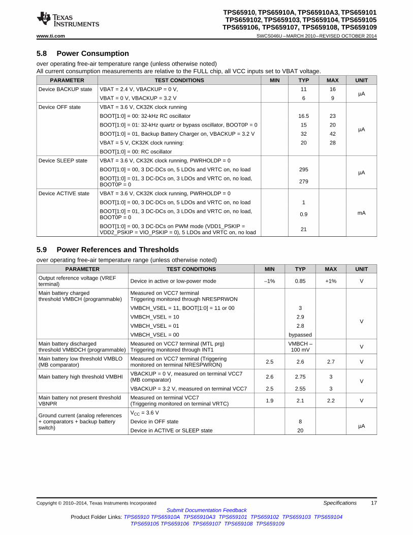
5.8 Power Consumptionover operating free-air temperature range (unless otherwise noted)All current consumption measurements are relative to the FULL chip, all VCC inputs set to VBAT voltage.
PARAMETER TEST CONDITIONS MIN TYP MAX UNITDevice BACKUP state VBAT = 2.4 V, VBACKUP = 0 V, 11 16
µAVBAT = 0 V, VBACKUP = 3.2 V 6 9
Device OFF state VBAT = 3.6 V, CK32K clock runningBOOT[1:0] = 00: 32-kHz RC oscillator 16.5 23BOOT[1:0] = 01: 32-kHz quartz or bypass oscillator, BOOT0P = 0 15 20
µABOOT[1:0] = 01, Backup Battery Charger on, VBACKUP = 3.2 V 32 42VBAT = 5 V, CK32K clock running: 20 28BOOT[1:0] = 00: RC oscillator
Device SLEEP state VBAT = 3.6 V, CK32K clock running, PWRHOLDP = 0BOOT[1:0] = 00, 3 DC-DCs on, 5 LDOs and VRTC on, no load 295 µABOOT[1:0] = 01, 3 DC-DCs on, 3 LDOs and VRTC on, no load, 279BOOT0P = 0
Device ACTIVE state VBAT = 3.6 V, CK32K clock running, PWRHOLDP = 0BOOT[1:0] = 00, 3 DC-DCs on, 5 LDOs and VRTC on, no load 1BOOT[1:0] = 01, 3 DC-DCs on, 3 LDOs and VRTC on, no load, mA0.9BOOT0P = 0BOOT[1:0] = 00, 3 DC-DCs on PWM mode (VDD1_PSKIP = 21VDD2_PSKIP = VIO_PSKIP = 0), 5 LDOs and VRTC on, no load
5.9 Power References and Thresholdsover operating free-air temperature range (unless otherwise noted)
PARAMETER TEST CONDITIONS MIN TYP MAX UNITOutput reference voltage (VREF Device in active or low-power mode –1% 0.85 +1% Vterminal)Main battery charged Measured on VCC7 terminalthreshold VMBCH (programmable) Triggering monitored through NRESPRWON
VMBCH_VSEL = 11, BOOT[1:0] = 11 or 00 3VMBCH_VSEL = 10 2.9
VVMBCH_VSEL = 01 2.8VMBCH_VSEL = 00 bypassed
Main battery discharged Measured on VCC7 terminal (MTL prg) VMBCH – Vthreshold VMBDCH (programmable) Triggering monitored through INT1 100 mVMain battery low threshold VMBLO Measured on VCC7 terminal (Triggering 2.5 2.6 2.7 V(MB comparator) monitored on terminal NRESPWRON)
VBACKUP = 0 V, measured on terminal VCC7Main battery high threshold VMBHI 2.6 2.75 3(MB comparator) VVBACKUP = 3.2 V, measured on terminal VCC7 2.5 2.55 3
Main battery not present threshold Measured on terminal VCC7 1.9 2.1 2.2 VVBNPR (Triggering monitored on terminal VRTC)VCC = 3.6 VGround current (analog references
+ comparators + backup battery Device in OFF state 8µAswitch) Device in ACTIVE or SLEEP state 20
Copyright © 2010–2014, Texas Instruments Incorporated Specifications 17Submit Documentation Feedback
Product Folder Links: TPS65910 TPS65910A TPS65910A3 TPS659101 TPS659102 TPS659103 TPS659104TPS659105 TPS659106 TPS659107 TPS659108 TPS659109

TPS65910, TPS65910A, TPS65910A3, TPS659101TPS659102, TPS659103, TPS659104, TPS659105TPS659106, TPS659107, TPS659108, TPS659109SWCS046U –MARCH 2010–REVISED OCTOBER 2014 www.ti.com
5.10 Thermal Monitoring and Shutdownover operating free-air temperature range (unless otherwise noted)
PARAMETER TEST CONDITIONS MIN TYP MAX UNITHot-die temperature rising threshold THERM_HDSEL[1:0] = 00 117
THERM_HDSEL[1:0] = 01 121°C
THERM_HDSEL[1:0] = 10 113 125 136THERM_HDSEL[1:0] = 11 130
Hot-die temperature hysteresis 10 °CThermal shutdown temperature rising 136 148 160 °CthresholdThermal shutdown temperature hysteresis 10 °C
Device in ACTIVE state, Temp = 27°C,Ground current 6 µAVCC7 = 3.6 V
5.11 32-kHz RTC Clockover operating free-air temperature range (unless otherwise noted)
PARAMETER TEST CONDITIONS MIN TYP MAX UNITCLK32KOUT rise and fall time CL = 35 pF 10 ns
Bypass Clock (OSC32KIN: input, OSC32KOUT floating)Input bypass clock frequency OSCKIN input 32 kHzInput bypass clock duty cycle OSCKIN input 40% 60%Input bypass clock rise and fall time 10% – 90%, OSC32KIN input 10 20 nsCLK32KOUT duty cycle Logic output signal 40% 60%Bypass clock setup time 32KCLKOUT output 1 msGround current Bypass mode 1.5 µA
Crystal oscillator (connected from OSC32KIN to OSC32KOUT)Output frequency CK32KOUT output 32.768 kHzOscillator startup time On power on 2 sGround current 1.5 µA
RC oscillator (OSC32KIN: grounded, OSC32KOUT floating)Output frequency CK32KOUT output 32 kHzOutput frequency accuracy at 25°C –15% 0% +15%Cycle jitter (RMS) Oscillator contribution +10%Output duty cycle +40% +50% +60%Settling time 150 µsGround current Active at fundamental frequency 4 µA
18 Specifications Copyright © 2010–2014, Texas Instruments IncorporatedSubmit Documentation Feedback
Product Folder Links: TPS65910 TPS65910A TPS65910A3 TPS659101 TPS659102 TPS659103 TPS659104TPS659105 TPS659106 TPS659107 TPS659108 TPS659109

TPS65910, TPS65910A, TPS65910A3, TPS659101TPS659102, TPS659103, TPS659104, TPS659105
TPS659106, TPS659107, TPS659108, TPS659109www.ti.com SWCS046U –MARCH 2010–REVISED OCTOBER 2014
5.12 Backup Battery Chargerover operating free-air temperature range (unless otherwise noted)
PARAMETER TEST CONDITIONS MIN TYP MAX UNITBackup battery charging current VBACKUP = 0 to 2.4 V, BBCHEN = 1 350 500 700 µAEnd-of-charge backup battery VCC7 = 3.6 V, BBSEL = 10 –3% 3.15 +3%voltage (1)
VCC7 = 3.6 V, BBSEL = 00 –3% 3 +3%V
VCC7 = 3.6 V, BBSEL = 01 –3% 2.52 +3%VBAT –VCC7 = 3.6 V, BBSEL = 11 VBAT0.3 V
Ground current On mode 10 µA
(1) Note:• BBSEL = 10, 00, or 01 intended to charge battery or superCap• BBSEL = 11 intended to charge capacitor
5.13 VRTC LDOover operating free-air temperature range (unless otherwise noted)
PARAMETER TEST CONDITIONS MIN TYP MAX UNITInput voltage VIN On mode 2.5 5.5
VBack-up mode 1.9 5.5
DC output voltage VOUT On mode, 3.0 V < VIN < 5.5 V 1.78 1.83 1.88V
Back-up mode, 2.3 V ≤ VIN ≤ 2.6 V 1.72 1.78 1.84Rated output current IOUTmax On mode 20
mABack-up mode 0.1
DC load regulation On mode, IOUT = IOUTmax to 0 50mV
Back-up mode, IOUT = IOUTmax to 0 50DC line regulation On mode, VIN = 3.0 V to VINmax at IOUT = IOUTmax 2.5
mVBack-up mode, VIN = 2.3 V to 5.5 V at IOUT = 25IOUTmax
Transient load regulation On mode, VIN = VINmin + 0.2 V to VINmax 50 (1) mVIOUT = IOUTmax/2 to IOUTmax in 5 µsand IOUT = IOUTmax to IOUTmax/2 in 5 µs
Transient line regulation On mode, VIN = VINmin + 0.5 V to VINmin in 30 µs 25 (1) mVAnd VIN = VINmin to VINmin + 0.5 V in 30 µs, IOUT =IOUTmax/2IOUT = 0, VIN rising from 0 up to 3.6 V, at VOUT =Turn-on time 2.2 ms0.1 V up to VOUTmin
VIN = VINDC + 100 mVpp tone, VINDC+ = VINmin +Ripple rejection 0.1 V to VINmax at IOUT = IOUTmax/2f = 217 Hz 55
dBf = 50 kHz 35
Ground current Device in ACTIVE state 23µA
Device in BACKUP or OFF state 3
(1) These parameters are not tested. They are used for design specification only.
Copyright © 2010–2014, Texas Instruments Incorporated Specifications 19Submit Documentation Feedback
Product Folder Links: TPS65910 TPS65910A TPS65910A3 TPS659101 TPS659102 TPS659103 TPS659104TPS659105 TPS659106 TPS659107 TPS659108 TPS659109

TPS65910, TPS65910A, TPS65910A3, TPS659101TPS659102, TPS659103, TPS659104, TPS659105TPS659106, TPS659107, TPS659108, TPS659109SWCS046U –MARCH 2010–REVISED OCTOBER 2014 www.ti.com
5.14 VIO SMPSover operating free-air temperature range (unless otherwise noted)PARAMETER TEST CONDITIONS MIN TYP MAX UNITInput voltage (VCCIO and VCC7) VIN IOUT ≤ 800 mA 2.7 5.5
VOUT = 1.5 V or 1.8 V, IOUT > 800 mA 3.2 5.5V
VOUT = 2.5 V, IOUT > 800 mA 4.0 5.5VOUT = 3.3 V, IOUT > 800 mA 4.4 5.5PWM mode (VIO_PSKIP = 0) or pulse skipDC output voltage (VOUT) mode IOUT to IMAX
VSEL=00 –3% 1.5 +3%VSEL = 01, default BOOT[1:0] = 00 and 01 –3% 1.8 +3%VSEL = 10 –3% 2.5 +3% VVSEL = 11 –3% 3.3 +3%Power down 0
Rated output current IOUTmax ILMAX[1:0] = 00, default 500mA
ILMAX[1:0] = 01 1000P-channel MOSFET VIN = VINmin 300
mΩOn-resistance RDS(ON)_PMOS VIN = 3.8 V 250 400P-channel leakage current ILK_PMOS VIN = VINMAX, SWIO = 0 V 2 µAN-channel MOSFET VIN = VMIN 300
mΩOn-resistance RDS(ON)_NMOS VIN = 3.8 V 250 400N-channel leakage current ILK_NMOS VIN = VINmax, SWIO = VINmax 2 µAPMOS current limit (high-side) VIN = VINmin to VINmax, ILMAX[1:0] = 00 650
VIN = VINmin to VINmax, ILMAX[1:0] = 01 1200 mAVIN = VINmin to VINmax, ILMAX[1:0] = 10 1700
NMOS current limit (low-side) Source current load:VIN = VINmin to VINmax, ILMAX[1:0] = 00 650VIN = VINmin to VINmax, ILMAX[1:0] = 01 1200VIN = VINmin to VINmax, ILMAX[1:0] = 10 1700
mASink current load:VIN = VINmin to VINmax, ILMAX[1:0] = 00 800VIN = VINmin to VINmax, ILMAX[1:0] = 01 1200VIN = VINmin to VINmax, ILMAX[1:0] = 10 1700
DC load regulation On mode, IOUT = 0 to IOUTmax 20 mVDC line regulation On mode, VIN = VINmin to VINmax 20 mV
VIN = 3.8 V, VOUT = 1.8 V50 mV
Transient load regulation IOUT = 0 to 500 mA , Max slew = 100 mA/µsIOUT = 700 to 1200 mA , Max slew = 100 mA/µs
t on, off to on IOUT = 200 mA 350 µsOvershoot SMPS turned on 3%
0.025 ×Power-save mode Ripple voltage Pulse skipping mode, IOUT = 1 mA VPPVOUT
Switching frequency 3 MHzDuty cycle 100 %Minimum On Time TON(MIN) 35 nsP-channel MOSFETVFBIO internal resistance 0.5 1 MΩDischarge resistor for power-down During device switch-off sequence 30 50 Ωsequence RDIS
Note: No discharge resistor is applied if VIO isturned off while the device is on.
20 Specifications Copyright © 2010–2014, Texas Instruments IncorporatedSubmit Documentation Feedback
Product Folder Links: TPS65910 TPS65910A TPS65910A3 TPS659101 TPS659102 TPS659103 TPS659104TPS659105 TPS659106 TPS659107 TPS659108 TPS659109

TPS65910, TPS65910A, TPS65910A3, TPS659101TPS659102, TPS659103, TPS659104, TPS659105
TPS659106, TPS659107, TPS659108, TPS659109www.ti.com SWCS046U –MARCH 2010–REVISED OCTOBER 2014
VIO SMPS (continued)over operating free-air temperature range (unless otherwise noted)PARAMETER TEST CONDITIONS MIN TYP MAX UNITGround current (IQ) Off 1
PWM mode, IOUT = 0 mA, VIN = 3.8 V, 7500VIO_PSKIP = 0Pulse skipping mode, no switching, 3-MHz clock µA250onLow-power (pulse skipping) mode, no switchingST[1:0]=11 63PWM mode, DCRL < 50 mΩ, VOUT = 1.8 V, VINConversion efficiency = 3.6 V:IOUT = 10 mA 44%IOUT = 100 mA 87%IOUT = 400 mA 86%IOUT = 800 mA 76%IOUT = 1000 mA 72%Pulse Skipping mode, DCRL < 50 mΩ, VOUT =1.8 V, VIN = 3.6 V:IOUT = 1 mA 71%IOUT = 10 mA 80%IOUT = 200 mA 87%
Copyright © 2010–2014, Texas Instruments Incorporated Specifications 21Submit Documentation Feedback
Product Folder Links: TPS65910 TPS65910A TPS65910A3 TPS659101 TPS659102 TPS659103 TPS659104TPS659105 TPS659106 TPS659107 TPS659108 TPS659109

TPS65910, TPS65910A, TPS65910A3, TPS659101TPS659102, TPS659103, TPS659104, TPS659105TPS659106, TPS659107, TPS659108, TPS659109SWCS046U –MARCH 2010–REVISED OCTOBER 2014 www.ti.com
5.15 VDD1 SMPSover operating free-air temperature range (unless otherwise noted)
PARAMETER TEST CONDITIONS MIN TYP MAX UNITInput voltage (VCC1 and VCC7) VIN IOUT ≤ 1200 mA 2.7 5.5
VOUT = 0.6 V to 1.5 V, VGAIN_SEL = 00, VOUT + 2 V 5.5IOUT > 1200 mA V2.5 V ≤ VOUT ≤ 3.3 V, VGAIN_SEL = 10 or 11, 4.5 5.5IOUT > 1200 mA
DC output voltage (VOUT) VGAIN_SEL = 00, IOUT = 0 to IOUTmax:max programmable voltage, SEL[6:0] = 1001011 1.5default voltage, BOOT[1:0] = 00 –3% 1.2 +3%default voltage, BOOT[1:0] = 01 –3% 1.2 +3% Vmin programmable voltage, SEL[6:0] = 0000011 0.6SEL[6:0] = 000000: power down 0VGAIN_SEL = 10, SEL = 0101011 = 43, IOUT = 0 –3% 2.2 +3% Vto IOUTmax
VGAIN_SEL = 11, SEL = 0101000 = 40, IOUT = 0 –3% 3.2 +3% Vto IOUTmax
DC output voltage programmable VGAIN_SEL = 00, 72 steps 12.5 mVstep (VOUTSTEP)Rated output current IOUTmax ILMAX = 0, default 1000 mA
ILMAX = 1 1500P-channel MOSFET VIN = VINmin 300
mΩOn-resistance RDS(ON)_PMOS VIN = 3.8 V 250 400P-channel leakage current VIN = VINmax, SW1 = 0 V 2 µAILK_PMOS
N-channel MOSFET VIN = VMIN 300mΩ
On-resistance RDS(ON)_NMOS VIN = 3.8 V 250 400N-channel leakage current ILK_NMOS VIN = VINmax, SW1 = VINmax 2 µAPMOS current limit (high-side) VIN = VINmin to VINmax, ILMAX = 0 1150
mAVIN = VINmin to VINmax, ILMAX = 1 2000
NMOS current limit (low-side) Source current load:VIN = VINmin to VINmax, ILMAX = 0 1150VIN = VINmin to VINmax, ILMAX = 1 2000
mASink current load:VIN = VINmin to VINmax, ILMAX = 0 1200VIN = VINmin to VINmax, ILMAX = 1 2000
DC load regulation On mode, IOUT = 0 to IOUTmax 20 mVDC line regulation On mode, VIN = VINmin to VINmax 20 mVTransient load regulation VIN = 3.8 V, VOUT = 1.2 V
IOUT = 0 to 500 mA , Max slew = 100 mA/µs 50 mVIOUT = 700 mA to 1.2A , Max slew = 100 mA/µs
t on, off to on IOUT = 200 mA 350 µsFrom VOUT = 0.6 V to 1.5 V and VOUT = 1.5 V toOutput voltage transition rate 0.6 V IOUT = 500 mATSTEP[2:0] = 001 12.5TSTEP[2:0] = 011 (default) 7.5 mV/µsTSTEP[2:0] = 111 2.5
Overshoot SMPS turned on 3%0.025 ×Power-save mode ripple voltage Pulse skipping mode, IOUT = 1 mA VPPVOUT
Switching frequency 3 MHz
22 Specifications Copyright © 2010–2014, Texas Instruments IncorporatedSubmit Documentation Feedback
Product Folder Links: TPS65910 TPS65910A TPS65910A3 TPS659101 TPS659102 TPS659103 TPS659104TPS659105 TPS659106 TPS659107 TPS659108 TPS659109

TPS65910, TPS65910A, TPS65910A3, TPS659101TPS659102, TPS659103, TPS659104, TPS659105
TPS659106, TPS659107, TPS659108, TPS659109www.ti.com SWCS046U –MARCH 2010–REVISED OCTOBER 2014
VDD1 SMPS (continued)over operating free-air temperature range (unless otherwise noted)
PARAMETER TEST CONDITIONS MIN TYP MAX UNITDuty cycle 100 %Minimum on time tON(MIN) 35 nsP-channel MOSFETVFB1 internal resistance 0.5 1 MΩDischarge resistor for power-down 30 50 Ωsequence RDIS
Ground current (IQ) Off 1PWM mode, IOUT = 0 mA, VIN = 3.8 V, 7500VDD1_PSKIP = 0
µAPulse skipping mode, no switching 78Low-power (pulse skipping) mode, no switchingST[1:0] = 11 63PWM mode, DCRL < 0.1 Ω, VOUT = 1.2 V,Conversion efficiency VIN = 3.6 V:IOUT = 10 mA 35%IOUT = 200 mA 82%IOUT = 400 mA 81%IOUT = 800 mA 74%IOUT = 1500 mA 62%Pulse skipping mode, DCRL < 0.1Ω, VOUT = 1.2V, VIN = 3.6 V:IOUT = 1 mA 59%IOUT = 10 mA 70%IOUT = 200 mA 82%
Copyright © 2010–2014, Texas Instruments Incorporated Specifications 23Submit Documentation Feedback
Product Folder Links: TPS65910 TPS65910A TPS65910A3 TPS659101 TPS659102 TPS659103 TPS659104TPS659105 TPS659106 TPS659107 TPS659108 TPS659109

TPS65910, TPS65910A, TPS65910A3, TPS659101TPS659102, TPS659103, TPS659104, TPS659105TPS659106, TPS659107, TPS659108, TPS659109SWCS046U –MARCH 2010–REVISED OCTOBER 2014 www.ti.com
5.16 VDD2 SMPSover operating free-air temperature range (unless otherwise noted)
PARAMETER TEST CONDITIONS MIN TYP MAX UNITInput voltage (VCC2 and VCC4) VIN IOUT ≤ 1200 mA 2.7 5.5
VOUT = 0.6 V to 1.5 V, VGAIN_SEL = 00, VOUT + 2 5.5IOUT > 1200 mA V V2.5 V ≤ VOUT ≤ 3.3 V, VGAIN_SEL = 10 or 11, 4.5 5.5IOUT > 1200 mA
DC output voltage (VOUT) VGAIN_SEL = 00, IOUT = 0 to IOUTmax:max programmable voltage, SEL[6:0] = 1001011 1.5default, BOOT[1:0] = 01 –3% 1.2 +3%min programmable voltage, SEL[6:0] = 0000011 0.6
VSEL[6:0] = 000000: power down 0VGAIN_SEL = 10, SEL = 0101011 = 43 –3% 2.2 +3%VGAIN_SEL = 11, default, BOOT[1:0] = 00 –3% 3.3 +3%
DC output voltage programmable VGAIN_SEL = 00, 72 steps 12.5 mVstep (VOUTSTEP)Rated output current IOUTmax ILMAX = 0, default 1000 mA
ILMAX = 1 1500P-channel MOSFET VIN = VINmin 300
mΩOn-resistance RDS(ON)_PMOS VIN = 3.8 V 250 400P-channel leakage current ILK_PMOS VIN = VINmax, SW2 = 0 V 2 µAN-channel MOSFET VIN = VMIN 300
mΩOn-resistance RDS(ON)_NMOS VIN = 3.8 V 250 400N-channel leakage current ILK_NMOS VIN = VINmax, SW2 = VINmax 2 µAPMOS current limit (high-side) VIN = VINmin to VINmax, ILMAX = 0 1150
mAVIN = VINmin to VINmax, ILMAX = 1 2200
NMOS current limit (low-side) Source current load: 1150VIN = VINmin to VINmax, ILMAX = 0 2000VIN = VINmin to VINmax, ILMAX = 1
mASink current load:VIN = VINmin to VINmax, ILMAX = 0 1200VIN = VINmin to VINmax, ILMAX = 1 2000
DC load regulation On mode, IOUT = 0 to IOUTmax 20 mVDC line regulation On mode, VIN = VINmin to VINmax at IOUT = IOUTmax 20 mVTransient load regulation VIN = 3.8 V, VOUT = 1.2 V 50 mV
IOUT = 0 to 500 mA , Max slew = 100 mA/µsIOUT = 700 mA to 1.2 A , Max slew = 100 mA/µs
t on, off to on IOUT = 200 mA 350 µsFrom VOUT = 0.6 V to 1.5 V and VOUT = 1.5 V toOutput voltage transition rate 0.6 V IOUT = 500 mATSTEP[2:0] = 001 12.5TSTEP[2:0] = 011 (default) 7.5 µsTSTEP[2:0] = 111 2.5
0.025Power-save mode ripple voltage Pulse skipping mode, IOUT = 1 mA VPPVOUT
Overshoot 3%Switching frequency 3 MHzDuty cycle 100 %Minimum On time
35 nsP-Channel MOSFET
24 Specifications Copyright © 2010–2014, Texas Instruments IncorporatedSubmit Documentation Feedback
Product Folder Links: TPS65910 TPS65910A TPS65910A3 TPS659101 TPS659102 TPS659103 TPS659104TPS659105 TPS659106 TPS659107 TPS659108 TPS659109

TPS65910, TPS65910A, TPS65910A3, TPS659101TPS659102, TPS659103, TPS659104, TPS659105
TPS659106, TPS659107, TPS659108, TPS659109www.ti.com SWCS046U –MARCH 2010–REVISED OCTOBER 2014
VDD2 SMPS (continued)over operating free-air temperature range (unless otherwise noted)
PARAMETER TEST CONDITIONS MIN TYP MAX UNITVFB2 internal resistance 0.5 1 MΩDischarge resistor for power-down 30 50 Ωsequence RDIS
Ground current (IQ) Off 1PWM mode, IOUT = 0 mA, VIN = 3.8 V, 7500VDD2_PSKIP = 0
µAPulse skipping mode, no switching 78Low-power (pulse skipping) mode, no switchingST[1:0] = 11 63PWM mode, DCRL < 50 mΩ, VOUT = 1.2 V,Conversion efficiency VIN = 3.6 V:IOUT = 10 mA 35%IOUT = 200 mA 82%IOUT = 400 mA 81%IOUT = 800 mA 74%IOUT = 1200 mA 66%IOUT = 1500 mA 62%Pulse skipping mode mode, DCRL < 50 mΩ, VOUT= 1.2 V, VIN = 3.6 V:IOUT = 1 mA 59%IOUT = 10 mA 70%IOUT = 200 mA 82%PWM mode, DCRL < 50 mΩ, VOUT = 3.3 V,VIN = 5 V:IOUT = 10 mA 44%IOUT = 200 mA 90%IOUT = 400 mA 91%IOUT = 800 mA 88%IOUT = 1200 mA 84%IOUT = 1500 mA 81%Pulse skipping mode mode, DCRL < 50 mΩ,VOUT = 3.3 V, VIN = 5 V:IOUT = 1 mA 75%IOUT = 10 mA 83%IOUT = 200 mA 90%
Copyright © 2010–2014, Texas Instruments Incorporated Specifications 25Submit Documentation Feedback
Product Folder Links: TPS65910 TPS65910A TPS65910A3 TPS659101 TPS659102 TPS659103 TPS659104TPS659105 TPS659106 TPS659107 TPS659108 TPS659109

TPS65910, TPS65910A, TPS65910A3, TPS659101TPS659102, TPS659103, TPS659104, TPS659105TPS659106, TPS659107, TPS659108, TPS659109SWCS046U –MARCH 2010–REVISED OCTOBER 2014 www.ti.com
5.17 VDD3 SMPSover operating free-air temperature range (unless otherwise noted)
PARAMETER TEST CONDITIONS MIN TYP MAX UNITInput voltage VIN 3 5.5 VDC output voltage (VOUT) 4.65 5 5.25 VRated output current IOUTmax 100 mAN-channel MOSFET VIN = 3.6 V 500 mΩOn-resistance RDS(ON)_NMOS
N-channel MOSFET leakage VIN = VINmax, SW3 = VINmax 2 µAcurrent ILK_NMOS
N-channel MOSFET DC current VIN = VINmin to VINmax, sink current load 430 550 mAlimitTurn-on inrush current VIN = VINmin to VINmax 850 mARipple voltage 20 mVDC load regulation On mode, IOUT = 0 to IOUTmax 100 mVDC line regulation On mode, VIN = VINmin to 5 V at IOUT = IOUTmax 100 mVTurn-on time IOUT = 8 mA, VOUT = 0 to 4.4 V 200 µsOvershoot 3%Switching frequency 1 MHzVFB3 internal resistance 088 MΩGround current (IQ) Off 1
µAIOUT = 0 mA to IOUTmax, VIN = 3.6 V 360
Conversion efficiency VIN = 3.6 V:IOUT = 10 mA 81%IOUT = 50 mA 85%IOUT = 100 mA 85%
26 Specifications Copyright © 2010–2014, Texas Instruments IncorporatedSubmit Documentation Feedback
Product Folder Links: TPS65910 TPS65910A TPS65910A3 TPS659101 TPS659102 TPS659103 TPS659104TPS659105 TPS659106 TPS659107 TPS659108 TPS659109

TPS65910, TPS65910A, TPS65910A3, TPS659101TPS659102, TPS659103, TPS659104, TPS659105
TPS659106, TPS659107, TPS659108, TPS659109www.ti.com SWCS046U –MARCH 2010–REVISED OCTOBER 2014
5.18 VDIG1 and VDIG2 LDOover operating free-air temperature range (unless otherwise noted)
PARAMETER TEST CONDITIONS MIN TYP MAX UNITVOUT (VDIG1) = 1.2 V at 300 mA / 1.5 V at 100Input voltage (VCC6) VIN mA andVOUT (VDIG2) = 1.2 V / 1.1 V / 1.0 V at 300 mA 1.7 5.5VOUT (VDIG1) = 1.5 V and VOUT (VDIG2) = 1.8 V V2.1 5.5at 200mAVOUT (VDIG1) = 1.8 V and VOUT (VDIG2) = 1.8 V 2.7 5.5VOUT (VDIG1) = 2.7 V 3.2 5
VDIG1DC output voltage VOUT On and Low-power mode, VIN = VINmin to VINmax
SEL = 11, IOUT = 0 to IOUTmax –3% 2.7 +3%SEL = 10 IOUT = 0 to IOUTmax –3% 1.8 +3%
VSEL = 01 IOUT = 0 to 100 mA/IOUTmax –3% 1.5 +3%SEL = 00, IOUT = 0 to IOUTmax, VIN = VINmin to 4 V, –3% 1.2 +3%default BOOT[1:0] = 00 or 01
Rated output current IOUTmax On mode 300mA
Low-power mode 1Load current limitation (short-circuit On mode, VOUT = VOUTmin – 100 mV 350 600 mAprotection)Dropout voltage VDO On mode, VDO = VIN – VOUT
VOUTtyp = 2.7 V, VIN = 2.8 V, IOUT = IOUTmax, T = 15025°CmV
VOUTtyp = 1.5 V, VIN = 1.7 V, IOUT = IOUTmax, T = 30025°CDC load regulation On mode, IOUT = IOUTmax to 0 25 mVDC line regulation On mode, VIN = VINmin to VINmax at IOUT = IOUTmax 3 mVTransient load regulation On mode, VIN = 3.8 V 10 mV
IOUT = 20 mA to 180 mA in 5µs andIOUT = 180 mA to 20 mA in 5 µs
Transient line regulation On mode, VIN = 2.7 + 0.5 V to 2.7 in 30 µs, 2 mVAnd VIN = 2.7 to 2.7 + 0.5 V in 30 µs, IOUT =IOUTmax/2
Turn-on time IOUT = 0, at VOUT = 0.1 V up to VOUTmin 100 µsTurn-on inrush current 300 mA
VIN = VINDC + 100 mVpp tone, VINDC+= 3.8 V, IOUT =Ripple rejection IOUTmax/2f = 217 Hz 70
dBf = 50 kHz 40
VDIG1 internal resistance LDO off 400 ΩGround current On mode, IOUT = 0, VCC6 = VBAT, VOUT = 2.7 V 54
On mode, IOUT = 0, VCC6 = 1.8 V, VOUT = 1.2 V 67On mode, IOUT = IOUTmax, VCC6 = VBAT, VOUT = 18702.7 VOn mode, IOUT = IOUTmax, VCC6 = 1.8 V, VOUT = µA13001.2 VLow-power mode, VCC6 = VBAT, VOUT = 2.7 V 13Low-power mode, VCC6 = 1.8 V, VOUT = 1.2 V 10Off mode 1
Copyright © 2010–2014, Texas Instruments Incorporated Specifications 27Submit Documentation Feedback
Product Folder Links: TPS65910 TPS65910A TPS65910A3 TPS659101 TPS659102 TPS659103 TPS659104TPS659105 TPS659106 TPS659107 TPS659108 TPS659109

TPS65910, TPS65910A, TPS65910A3, TPS659101TPS659102, TPS659103, TPS659104, TPS659105TPS659106, TPS659107, TPS659108, TPS659109SWCS046U –MARCH 2010–REVISED OCTOBER 2014 www.ti.com
VDIG1 and VDIG2 LDO (continued)over operating free-air temperature range (unless otherwise noted)
PARAMETER TEST CONDITIONS MIN TYP MAX UNITVDIG2
DC output voltage VOUT On and low-power mode, VIN = VINmin to VINmax
SEL = 11, IOUT = 0 to IOUTmax –3% 1.8 +3%SEL = 10 IOUT = 0 to IOUTmax, VIN = VINmin to 4 V –3% 1.2 +3%SEL = 01 IOUT = 0 to 100 mA/IOUTmax, VIN= VINmin V–3% 1.1 +3%to 4 VSEL = 00, IOUT = 0 to IOUTmax, VIN = VINmin to 4 V, –3% 1 +3%default BOOT[1:0] = 00 or 01
Rated output current IOUTmax On mode 300 mALow-power mode 1
Load current limitation (short-circuit On mode, VOUT = VOUTmin – 100 mV 350 600 mAprotection)Dropout voltage VDO On mode, VDO = VIN – VOUT,
VOUTtyp = 1.8 V, VIN = 2.1 V, IOUT=IOUTmax, T = 250 mV25°CDC load regulation On mode, IOUT = IOUTmax to 0 25 mVDC line regulation On mode, VIN = VINmin to VINmax at IOUT = IOUTmax 3 mVTransient load regulation On mode, VIN = 3.8 V 10 mV
IOUT = 20 mA to 180 mA in 5 µs andIOUT = 180 mA to 20 mA in 5 µs
Transient line regulation On mode, VIN = 2.7 + 0.5 V to 2.7 in 30 µs, 2 mVAnd VIN = 2.7 to 2.7 + 0.5 V in 30 µs, IOUT =IOUTmax/2
Turn-on time IOUT = 0, at VOUT = 0.1 V up to VOUTmin 100 µsTurn-on inrush current 300 mA
VIN = VINDC + 100 mVpp tone, VINDC+= 3.8 V, IOUT =Ripple rejection IOUTmax/2f = 217 Hz 70
dBf = 50 kHz 40
VDIG2 internal resistance LDO off 400 ΩGround current On mode, IOUT = 0, VCC6 = VBAT, VOUT = 1.8 V 52
On mode, IOUT = 0, VCC6 = 1.8 V, VOUT = 1.0 V 67On mode, IOUT = IOUTmax, VCC6 = VBAT, VOUT = 17501.8 VOn mode, IOUT = IOUTmax, VCC6 = 1.8 V, VOUT = µA13001.0 VLow-power mode, VCC6 = VBAT, VOUT = 1.8 V 11Low-power mode, VCC6 = 1.8 V, VOUT = 1.0 V 10Off mode 1
28 Specifications Copyright © 2010–2014, Texas Instruments IncorporatedSubmit Documentation Feedback
Product Folder Links: TPS65910 TPS65910A TPS65910A3 TPS659101 TPS659102 TPS659103 TPS659104TPS659105 TPS659106 TPS659107 TPS659108 TPS659109

TPS65910, TPS65910A, TPS65910A3, TPS659101TPS659102, TPS659103, TPS659104, TPS659105
TPS659106, TPS659107, TPS659108, TPS659109www.ti.com SWCS046U –MARCH 2010–REVISED OCTOBER 2014
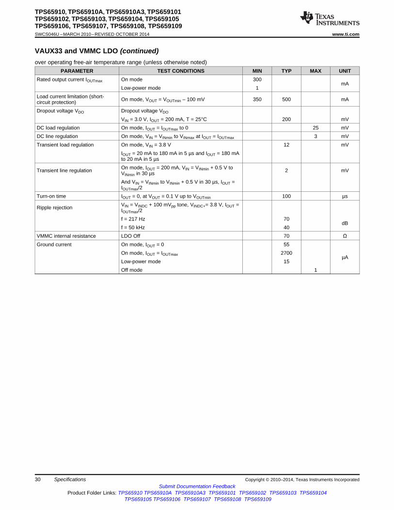
5.19 VAUX33 and VMMC LDOover operating free-air temperature range (unless otherwise noted)
PARAMETER TEST CONDITIONS MIN TYP MAX UNITVOUT (VAUX33) = 1.8 V / 2 V and VOUT (VMMC) =Input voltage (VCC3) VIN 2.7 5.51.8 VVOUT (VAUX33) = 2.8 V 3.2 5.5VOUT (VAUX33) = 3.3 V 3.6 5.5 VVOUT (VMMC) = 2.8 V at 200 mA 3.2 5.5VOUT (VMMC) = 3.0 V 3.6 5.5VOUT (VMMC) = 3.3 V at 200 mA 3.6 5.5
VAUX33DC output voltage VOUT On and low-power mode, VIN = VINmin to VINmax
SEL = 11, IOUT = 0 to IOUTmax, Default BOOT[1:0] = –3% 3.3 +3%01SEL = 10, IOUT = 0 to IOUTmax –3% 2.8 +3%
VSEL = 01, IOUT = 0 to IOUTmax –3% 2.0 +3%SEL = 00, IOUT = 0 to IOUTmax, default BOOT[1:0] = –3% 1.8 +3%00
Rated output current IOUTmax On mode 150mA
Low-power mode 1Load current limitation (short- On mode, VOUT = VOUTmin – 100 mV 350 500 mAcircuit protection)Dropout Voltage VDO On mode, VOUTtyp = 2.8 V, VDO = VIN – VOUT,
VIN = 2.9 V, IOUT = IOUTmax, T = 25°C 150 mVDC load regulation On mode, IOUT = IOUTmax to 0 20 mVDC line regulation On mode, IOUT = IOUTmax 3 mVTransient load regulation On mode, VIN = 3.8 V 12 mV
IOUT = 0.1 × IOUTmax to 0.9 × IOUTmax in 5 µs andIOUT = 0.9 × IOUTmax to 0.1 × IOUTmax in 5 µsOn mode, IOUT = IOUTmax,VIN = VINmin + 0.5 V toTransient line regulation 2 mVVINmin in 30 µsand VIN = VINmin to VINmin + 0.5 V in 30 µs, IOUT =IOUTmax/2
Turn-on time IOUT = 0, at VOUT = 0.1 V up to VOUTmin 100 µsTurn-on inrush current 600 mA
VIN = VINDC + 100 mVpp tone, VINDC+ = 3.8 V, IOUTRipple Rejection = IOUTmax/2f = 217 Hz 70
dBf = 50 kHz 40
VAUX33 internal resistance LDO off 70 ΩGround current On mode, IOUT = 0 55
On mode, IOUT = IOUTmax 1600µA
Low-power mode 15Off mode 1
VMMCDC output voltage VOUT On and low-power mode, VIN = VINmin to VINmax
SEL = 11, IOUT = 0 to 200 mA, default BOOT[1:0] = –3% 3.3 +3%00SEL = 10, IOUT = 0 to IOUTmax –3% 3.0 +3%
VSEL = 01, IOUT = 0 to 200 mA –3% 2.8 +3%SEL = 00, IOUT = 0 to IOUTmax, default BOOT[1:0] = –3% 1.8 +3%01
Copyright © 2010–2014, Texas Instruments Incorporated Specifications 29Submit Documentation Feedback
Product Folder Links: TPS65910 TPS65910A TPS65910A3 TPS659101 TPS659102 TPS659103 TPS659104TPS659105 TPS659106 TPS659107 TPS659108 TPS659109
TPS65910, TPS65910A, TPS65910A3, TPS659101TPS659102, TPS659103, TPS659104, TPS659105TPS659106, TPS659107, TPS659108, TPS659109SWCS046U –MARCH 2010–REVISED OCTOBER 2014 www.ti.com
VAUX33 and VMMC LDO (continued)over operating free-air temperature range (unless otherwise noted)
PARAMETER TEST CONDITIONS MIN TYP MAX UNITRated output current IOUTmax On mode 300
mALow-power mode 1
Load current limitation (short- On mode, VOUT = VOUTmin – 100 mV 350 500 mAcircuit protection)Dropout voltage VDO Dropout voltage VDO
VIN = 3.0 V, IOUT = 200 mA, T = 25°C 200 mVDC load regulation On mode, IOUT = IOUTmax to 0 25 mVDC line regulation On mode, VIN = VINmin to VINmax at IOUT = IOUTmax 3 mVTransient load regulation On mode, VIN = 3.8 V 12 mV
IOUT = 20 mA to 180 mA in 5 µs and IOUT = 180 mAto 20 mA in 5 µsOn mode, IOUT = 200 mA, VIN = VINmin + 0.5 V toTransient line regulation 2 mVVINmin in 30 µsAnd VIN = VINmin to VINmin + 0.5 V in 30 µs, IOUT =IOUTmax/2
Turn-on time IOUT = 0, at VOUT = 0.1 V up to VOUTmin 100 µsVIN = VINDC + 100 mVpp tone, VINDC+= 3.8 V, IOUT =Ripple rejection IOUTmax/2f = 217 Hz 70
dBf = 50 kHz 40
VMMC internal resistance LDO Off 70 ΩGround current On mode, IOUT = 0 55
On mode, IOUT = IOUTmax 2700µA
Low-power mode 15Off mode 1
30 Specifications Copyright © 2010–2014, Texas Instruments IncorporatedSubmit Documentation Feedback
Product Folder Links: TPS65910 TPS65910A TPS65910A3 TPS659101 TPS659102 TPS659103 TPS659104TPS659105 TPS659106 TPS659107 TPS659108 TPS659109

TPS65910, TPS65910A, TPS65910A3, TPS659101TPS659102, TPS659103, TPS659104, TPS659105
TPS659106, TPS659107, TPS659108, TPS659109www.ti.com SWCS046U –MARCH 2010–REVISED OCTOBER 2014
5.20 VAUX1 and VAUX2 LDOover operating free-air temperature range (unless otherwise noted)
PARAMETER TEST CONDITIONS MIN TYP MAX UNITInput voltage (VCC4) VIN VOUT (VAUX1) = 1.8 V and VOUT (AUX2) = 1.8 V 2.7 5.5
VOUT (VAUX1) = 2.5 V 3.2 5.5VOUT (VAUX1) = 2.8 V at Iload = 200 mA and 2.85 V 3.2 5.5at Iload = 200mA VVOUT (VAUX2) = 2.8 V 3.2 5.5VOUT (VAUX2) = 2.9 V at Iload = 100mA 3.2 5.5VOUT (VAUX2) = 3.3 V 3.6 5.5
VAUX1DC output voltage VOUT On and low-power mode, VIN = VINmin to VINmax
SEL = 11, IOUT = 0 to 200 mA –3% 2.85 +3%SEL = 10, IOUT = 0 to 200 mA –3% 2.8 +3%
VSEL = 01, IOUT = 0 to IOUTmax –3% 2.5 +3%SEL = 00, IOUT = 0 to IOUTmax, default BOOT[1:0] = –3% 1.8 +3%00 or 01
Rated output current IOUTmax On mode 300mA
Low-power mode 1Load current limitation (short- On mode, VOUT = VOUTmin – 100 mV 350 500 mAcircuit protection)Dropout voltage VDO On mode, VOUTtyp = 2.8 V, VDO = VIN – VOUT,
VIN = 3.0 V, IOUT = 200 mA, T = 25°C 200 mVDC load regulation On mode, IOUT = 200 mA to 0 15 mADC line regulation On mode, IOUT = 200 mA 5 V
On mode, VIN = 3.8 V, IOUT = 20 mA to 180 mA in 5Transient load regulation 15 mVµsand IOUT = 180 mA to 20 mA in 5µsOn mode, IOUT = 200 mA, VIN= VINmin + 0.5 V toTransient line regulation 2 mVVINmin in 30 µsand VIN = VINmin to VINmin + 0.5v in 30 µs, IOUT =IOUTmax/2
Turn-on time IOUT = 0, at VOUT = 0.1 V up to VOUTmin, no load 100 µsTurn-on inrush current 600 mA
VIN = VINDC + 100 mVpp tone, VINDC+ = 3.8 V, IOUT =Ripple Rejection IOUTmax/2f = 217 Hz 70
dBf = 50 kHz 40
VAUX1 internal resistance LDO Off 80 ΩGround current On mode, IOUT = 0 60
On mode, IOUT = IOUTmax 2700µA
Low-power mode 12Off mode 1
VAUX2On and low-power mode, VIN = VINmin to VINmax
SEL = 11, IOUT = 0 to IOUTmax –3% 3.3 +3%SEL = 10, IOUT = 0 to 100 mA –3% 2.9 +3%
VSEL = 01, IOUT = 0 to IOUTmax –3% 2.8 +3%SEL = 00, IOUT = 0 to IOUTmax, default BOOT[1:0] = –3% 1.8 +3%00 or 01
Rated output current IOUTmax On mode 300mA
Low-power mode 1
Copyright © 2010–2014, Texas Instruments Incorporated Specifications 31Submit Documentation Feedback
Product Folder Links: TPS65910 TPS65910A TPS65910A3 TPS659101 TPS659102 TPS659103 TPS659104TPS659105 TPS659106 TPS659107 TPS659108 TPS659109

TPS65910, TPS65910A, TPS65910A3, TPS659101TPS659102, TPS659103, TPS659104, TPS659105TPS659106, TPS659107, TPS659108, TPS659109SWCS046U –MARCH 2010–REVISED OCTOBER 2014 www.ti.com
VAUX1 and VAUX2 LDO (continued)over operating free-air temperature range (unless otherwise noted)
PARAMETER TEST CONDITIONS MIN TYP MAX UNITLoad current limitation (short- On mode, VOUT = VOUTmin – 100 mV 350 500 mAcircuit protection)Dropout voltage VDO On mode, VOUTtyp = 2.8 V, VDO = VIN – VOUT 150 mV
VIN = 2.9 V, IOUT = IOUTmax, T = 25°CDC load regulation On mode, IOUT = IOUTmax to 0 15 mVDC line regulation On mode, VIN = VINmin to VINmax at IOUT = IOUTmax 2 mV
On mode, VIN = 3.8 V, IOUT = 0.1 × IOUTmax to 0.9 ×Transient load regulation 12 mVIOUTmax in 5µsAnd IOUT = 0.9 × IOUTmax to 0.1 × IOUTmax in 5usOn mode, IOUT = IOUTmax, VIN = VINmin + 0.5 V toTransient line regulation 2 mVVINmin in 30 µsAnd VIN= VINmin to VINmin + 0.5 V in 30 µs, IOUT =IOUTmax/2
Turn-on time IOUT = 0, at VOUT = 0.1 V up to VOUTmin 100 µsTurn-on Inrush current 600 mA
VIN = VINDC + 100 mVpp tone, VINDC+ = 3.8 V, IOUT =Ripple rejection IOUTmax/2f = 217 Hz 70
dBf = 50 kHz 40
VAUX2 internal resistance LDO off 80 ΩGround current On mode, IOUT = 0 60
On mode, IOUT = IOUTmax 1600µA
Low-power mode 12Off mode 1
32 Specifications Copyright © 2010–2014, Texas Instruments IncorporatedSubmit Documentation Feedback
Product Folder Links: TPS65910 TPS65910A TPS65910A3 TPS659101 TPS659102 TPS659103 TPS659104TPS659105 TPS659106 TPS659107 TPS659108 TPS659109

TPS65910, TPS65910A, TPS65910A3, TPS659101TPS659102, TPS659103, TPS659104, TPS659105
TPS659106, TPS659107, TPS659108, TPS659109www.ti.com SWCS046U –MARCH 2010–REVISED OCTOBER 2014
5.21 VDAC and VPLL LDOover operating free-air temperature range (unless otherwise noted)
PARAMETER TEST CONDITIONS MIN TYP MAX UNITVOUT(VDAC) = 1.8 V and VOUT(VPLL) = 1.8 V / 1.1 VInput voltage (VCC5) VIN 2.7 5.5/ 1.0 V
VVOUT(VDAC) = 2.6 V and VOUT(VPLL) = 2.5 V 3.0 5.5VOUT(VDAC) = 2.8 V / 2.85 V 3.2 5.5
VDACDC Output voltage VOUT On and low-power mode, VIN = VINmin to VINmax
SEL = 11, IOUT = 0 to IOUTmax –3% 2.85 +3%SEL = 10, IOUT = 0 to IOUTmax –3% 2.8 +3%
VSEL = 01, IOUT = 0 to IOUTmax –3% 2.6 +3%SEL = 00, IOUT = 0 to IOUTmax, default BOOT[1:0] = –3% 1.8 +3%00 or 01
Rated output current IOUTmax On mode 150mA
Low-power mode 1Load current limitation (short- On mode, VOUT = VOUTmin – 100 mV 350 500 mAcircuit protection)Dropout Voltage VDO On mode, VOUTtyp = 2.8 V, VDO = VIN – VOUT, 150 mV
VIN = 2.9 V, IOUT = IOUTmax, T = 25°CDC load regulation On mode, VOUT = VOUTmin – 100 mV 15 mVDC line regulation On mode, VOUT = 1.8 V, IOUT = IOUTmax 2 mV
On mode, VIN = 3.8 V, IOUT = 0.1 × IOUTmax to 0.9 ×Transient load regulation 15 mVIOUTmax in 5 µsAnd IOUT = 0.9 × IOUTmax to 0.1 × IOUTmax in 5 µsOn mode, IOUT = IOUTmax, VIN = VINmin + 0.5 V toTransient line regulation 0.5 mVVINmin in 30 µsAnd VIN = VINmin to VINmin + 0.5 V in 30 µs, IOUT =IOUTmax/2
Turn-on time IOUT = 0, at VOUT = 0.1 V up to VOUTmin 100 µsTurn-on Inrush current 600 mA
VIN = VINDC + 100 mVpp tone, VINDC+ = 3.8 V, IOUT =Ripple Rejection IOUTmax/2f = 217 Hz 70
dBf = 50 kHz 40
VDAC internal resistance LDO off 360 kΩGround current On mode, IOUT = 0 60
On mode, IOUT = IOUTmax 1600µA
Low-power mode 12Off mode 1
Copyright © 2010–2014, Texas Instruments Incorporated Specifications 33Submit Documentation Feedback
Product Folder Links: TPS65910 TPS65910A TPS65910A3 TPS659101 TPS659102 TPS659103 TPS659104TPS659105 TPS659106 TPS659107 TPS659108 TPS659109

TPS65910, TPS65910A, TPS65910A3, TPS659101TPS659102, TPS659103, TPS659104, TPS659105TPS659106, TPS659107, TPS659108, TPS659109SWCS046U –MARCH 2010–REVISED OCTOBER 2014 www.ti.com
VDAC and VPLL LDO (continued)over operating free-air temperature range (unless otherwise noted)
PARAMETER TEST CONDITIONS MIN TYP MAX UNITVPLL
DC output voltage VOUT On and low-power mode, VIN = VINmin to VINmax
SEL = 11, IOUT = 0 to IOUTmax –3% 2.5 +3%SEL = 10, IOUT = 0 to IOUTmax, default BOOT[1:0 = 00 –3% 1.8 +3%or 01 VSEL = 01, IOUT = 0 to IOUTmax –3% 1.1 +3%SEL = 00, IOUT = 0 to IOUTmax –3% 1.0 +3%
Rated output current IOUTmax On mode 50mA
Low-power mode 1Load current limitation (short- On mode, VOUT = VOUTmin – 100 mV 200 400 mAcircuit protection)Dropout voltage VDO On mode, VOUTtyp = 2.5 V, VDO = VIN – VOUT, 100 mV
VIN = 2.5 V, IOUT = IOUTmax, T = 25°CDC load regulation On mode, IOUT = IOUTmax to 0 10 mVDC line regulation On mode, VIN = VINmin to VINmax at IOUT = IOUTmax 1 mV
On mode, VIN = 3.8 V, IOUT = 0.1 × IOUTmax to 0.9 ×Transient load regulation 9 mVIOUTmax in 5 µsAnd IOUT = 0.9 × IOUTmax to 0.1 × IOUTmax in 5 µs
Transient line regulation On mode, VIN = VINmin + 0.5 V to VINmin in 30 µs 0.5 mVAnd VIN = VINmin to VINmin + 0.5 V in 30 µs, IOUT =IOUTmax/2
Turn-on time IOUT = 0, at VOUT = 0.1 V up to VOUTmin 100 µsTurn-on in rush current 300 mA
VIN = VINDC + 100 mVpp tone, VINDC+ = 3.8 V, IOUT =Ripple rejection IOUTmax/2f = 217 Hz 70
dBf = 50 kHz 40
VPLL internal resistance LDO off 535 kΩGround current On mode, IOUT = 0 60
On mode, IOUT = IOUTmax 1600µA
Low-power mode 12Off mode 1
34 Specifications Copyright © 2010–2014, Texas Instruments IncorporatedSubmit Documentation Feedback
Product Folder Links: TPS65910 TPS65910A TPS65910A3 TPS659101 TPS659102 TPS659103 TPS659104TPS659105 TPS659106 TPS659107 TPS659108 TPS659109

TPS65910, TPS65910A, TPS65910A3, TPS659101TPS659102, TPS659103, TPS659104, TPS659105
TPS659106, TPS659107, TPS659108, TPS659109www.ti.com SWCS046U –MARCH 2010–REVISED OCTOBER 2014
5.22 Timing and Switching Characteristics
5.22.1 Switch-On/-Off Sequences and TimingTime slot length can be selected to be 0.5 ms or 2 ms through the EEPROM for an OFF-to-ACTIVE transition orthrough the value programmed in the register DEVCTRL2_REG for a SLEEP-to-ACTIVE transition.
5.22.1.1 BOOT1 = 0, BOOT0 = 0
Table 5-1 provides details about the EEPROM setting for the BOOT modes. The power-up sequence for thisboot mode is provided in Figure 5-1.
Table 5-1. Fixed Boot Mode: 00
TPS65910Register Bit Description Boot 00VDD1_OP_REG SEL VDD1 voltage level selection for boot 1.2 VVDD1_REG VGAIN_SEL VDD1 gain selection, x1 or x2 x1EEPROM VDD1 time slot selection 3DCDCCTRL_REG VDD1_PSKIP VDD1 pulse skip mode enable skip enabledVDD2_OP_REG/VDD2_SR_REG SEL VDD2 voltage level selection for boot 1.1 VVDD2_REG VGAIN_SEL VDD2 Gain selection, x1 or x3 x3EEPROM VDD2 time slot selection 2DCDCCTRL_REG VDD2_PSKIP VDD2 pulse skip mode enable skip enabledVIO_REG SEL VIO voltage selection 1.8 VEEPROM VIO time slot selection 1DCDCCTRL_REG VIO_PSKIP VIO pulse skip mode enable skip enabledEEPROM VDD3 time slot OFFVDIG1_REG SEL LDO voltage selection 1.2 VEEPROM LDO time slot OFFVDIG2_REG SEL LDO voltage selection 1.0 VEEPROM LDO time slot OFFVDAC_REG SEL LDO voltage selection 1.8 VEEPROM LDO time slot 5VPLL_REG SEL LDO voltage selection 1.8 VEEPROM LDO time slot 4VAUX1_REG SEL LDO voltage selection 1.8 VEEPROM LDO time slot 1VMMC_REG SEL LDO voltage selection 3.3 VEEPROM LDO time slot 6VAUX33_REG SEL LDO voltage selection 1.8 VEEPROM LDO time slot OFFVAUX2_REG SEL LDO voltage selection 1.8 VEEPROM LDO time slot 5CLK32KOUT pin CLK32KOUT time slot 7NRESPWRON pin NRESPWRON time slot 7 + 1
0: VRTC LDO will be in low-power mode during OFF stateVRTC_OFFMASVRTC_REG Low-power modeK 1: VRC LDO will be in full-power mode during OFF state0: RTC in normal power mode
DEVCTRL_REG RTC_PWDN 11: Clock gating of RTC register and logic, low-power mode0: Clock source is crystal/external clock
DEVCTRL_REG CK32K_CTRL RC1: Clock source is internal RC oscillator
Copyright © 2010–2014, Texas Instruments Incorporated Specifications 35Submit Documentation Feedback
Product Folder Links: TPS65910 TPS65910A TPS65910A3 TPS659101 TPS659102 TPS659103 TPS659104TPS659105 TPS659106 TPS659107 TPS659108 TPS659109

SWCS046-018
PWRHOLD
VIO/VFBIO
VAUX1
VDD2/VFB2
VDD1/VFB1
VPLL
VDAC
VAUX2
VMMC
CLK32KOUT
NRESPWRON
tdSOFF2
tdSON1
1.8 V
1.8 V
3.3 V
tdSON2
tdSON3
1.2 V
1.8 V
1.8 V
tdSON4
tdSON5
1.8 V
tdSON6
tdSON7
3.3 V
tdSON8
tdSOFF1
Switch-off sequencet : Switch-on sequencedSONT
TPS65910, TPS65910A, TPS65910A3, TPS659101TPS659102, TPS659103, TPS659104, TPS659105TPS659106, TPS659107, TPS659108, TPS659109SWCS046U –MARCH 2010–REVISED OCTOBER 2014 www.ti.com
Table 5-1. Fixed Boot Mode: 00 (continued)TPS65910Register Bit Description Boot 00
Boot sequence time slot duration:TSLOT_LENGTHDEVCTRL2_REG 0: 0.5 ms 2 ms[0]
1: 2 ms0: INT1 signal will be active-low
DEVCTRL2_REG IT_POL Active-low1: INT1 signal will be active-high0: Device will automatically switch-on at NOSUPPLY to 0: AutomaticOFF or BACKUP to OFF transitionINT_MSK_REG VMBHI_IT_MSK switch-on from
supply insertion1: Startup reason required before switch-onSelect threshold for main battery comparator thresholdVMBCH_REG VMBCH_SEL[1:0] 3 VVMBCH.
Figure 5-1 shows the 00 Boot mode timing characteristics.
Figure 5-1. Boot Mode: BOOT1 = 0, BOOT0 = 0
36 Specifications Copyright © 2010–2014, Texas Instruments IncorporatedSubmit Documentation Feedback
Product Folder Links: TPS65910 TPS65910A TPS65910A3 TPS659101 TPS659102 TPS659103 TPS659104TPS659105 TPS659106 TPS659107 TPS659108 TPS659109

TPS65910, TPS65910A, TPS65910A3, TPS659101TPS659102, TPS659103, TPS659104, TPS659105
TPS659106, TPS659107, TPS659108, TPS659109www.ti.com SWCS046U –MARCH 2010–REVISED OCTOBER 2014
Table 5-2 lists the 00 Boot mode timing characteristics.
Table 5-2. Boot Mode: BOOT1 = 0, BOOT0 = 0 Timing Characteristics
PARAMETER TEST CONDITIONS MIN TYP MAX UNITtdSON1 PWRHOLD rising edge to VIO, VAUX1 enable delay 66 × tCK32k = 2060 µstdSON2 VIO to VDD2 enable delay 64 × tCK32k = 2000 µstdSON3 VDD2 to VDD1 enable delay 64 × tCK32k = 2000 µstdSON4 VDD1 to VPLL enable delay 64 × tCK32k = 2000 µstdSON5 VPLL to VDAC,VAUX2 enable delay 64 × tCK32k = 2000 µstdSON6 VDAC to VMMC enable delay 64 × tCK32k = 2000 µs
VMMC to CLK32KOUT rising edge delay 64 × tCK32k = 2000 µstdSON8 CLK32KOUT to NRESPWRON rising edge delay 64 × tCK32k = 2000 µstdSONT Total switch-on delay 16 ms
PWRHOLD falling edge to NRESPWRON falling edgetdSOFF1 2 × tCK32k = 62.5 µsdelaytdSOFF1B NRESPWRON falling edge to CLK32KOUT low delay 3 × tCK32k = 92 µs
PWRHOLD falling edge to supplies and referencetdSOFF2 5 × tCK32k = 154 µsdisable delay
Registers default setting: CK32K_CTRL = 1 (32-kHz RC oscillator is used), RTC_PWDN = 1 (RTC domain off),IT_POL = 0 (INt2 interrupt flag active low), VMBHI_IT_MSK = 0 (automatic switch-on on Battery plug),VMBCH_SEL = 11.
Copyright © 2010–2014, Texas Instruments Incorporated Specifications 37Submit Documentation Feedback
Product Folder Links: TPS65910 TPS65910A TPS65910A3 TPS659101 TPS659102 TPS659103 TPS659104TPS659105 TPS659106 TPS659107 TPS659108 TPS659109

TPS65910, TPS65910A, TPS65910A3, TPS659101TPS659102, TPS659103, TPS659104, TPS659105TPS659106, TPS659107, TPS659108, TPS659109SWCS046U –MARCH 2010–REVISED OCTOBER 2014 www.ti.com
5.22.1.2 BOOT1 = 0, BOOT0 = 1
Table 5-3 provides details about the EEPROM setting for the BOOT modes. The power-up sequence for thisboot mode is provided in Figure 5-2.
Table 5-3. Fixed Boot Mode: 01
TPS65910Register Bit Description Boot 01VDD1_OP_REG SEL VDD1 voltage level selection for boot 1.2 VVDD1_REG VGAIN_SEL VDD1 Gain selection, x1 or x2 x1EEPROM VDD1 time slot selection 3DCDCCTRL_REG VDD1_PSKIP VDD1 pulse skip mode enable Skip enabledVDD2_OP_REG/VDD2_SR_REG SEL VDD2 voltage level selection for boot 1.2 VVDD2_REG VGAIN_SEL VDD2 Gain selection, x1 or x3 x1EEPROM VDD2 time slot selection 4DCDCCTRL_REG VDD2_PSKIP VDD2 pulse skip mode enable Skip enabledVIO_REG SEL VIO voltage selection 1.8 VEEPROM VIO time slot selection 1DCDCCTRL_REG VIO_PSKIP VIO pulse skip mode enable Skip enabledEEPROM VDD3 time slot OFFVDIG1_REG SEL LDO voltage selection 1.2 VEEPROM LDO time slot OFFVDIG2_REG SEL LDO voltage selection 1.0 VEEPROM LDO time slot OFFVDAC_REG SEL LDO voltage selection 1.8 VEEPROM LDO time slot OFFVPLL_REG SEL LDO voltage selection 1.8 VEEPROM LDO time slot 2VAUX1_REG SEL LDO voltage selection 1.8 VEEPROM LDO time slot OFFVMMC_REG SEL LDO voltage selection 1.8 VEEPROM LDO time slot OFFVAUX33_REG SEL LDO voltage selection 3.3 VEEPROM LDO time slot 6VAUX2_REG SEL LDO voltage selection 1.8 VEEPROM LDO time slot 5CLK32KOUT pin CLK32KOUT time slot 7NRESPWRON pin NRESPWRON time slot 7+1
0: VRTC LDO will be in low-power mode during OFF stateVRTC_OFFMASVRTC_REG low-power modeK 1: VRC LDO will be in full-power mode during OFF state0: RTC in normal power mode
DEVCTRL_REG RTC_PWDN 11: Clock gating of RTC register and logic, low-power mode0: Clock source is crystal/external clock
DEVCTRL_REG CK32K_CTRL Crystal1: Clock source is internal RC oscillatorBoot sequence time slot duration:
TSLOT_LENGTHDEVCTRL2_REG 0: 0.5 ms 2 ms[0]1: 2 ms0: INT1 signal will be active-low
DEVCTRL2_REG IT_POL Active-low1: INT1 signal will be active-high
38 Specifications Copyright © 2010–2014, Texas Instruments IncorporatedSubmit Documentation Feedback
Product Folder Links: TPS65910 TPS65910A TPS65910A3 TPS659101 TPS659102 TPS659103 TPS659104TPS659105 TPS659106 TPS659107 TPS659108 TPS659109

tdSON1
1.8 V
tdSON7
SWCS046-019
tdSON8
Switch-off sequencet : Switch-on sequencedSONT
1.8 V
1.2 V
3.3 V
1.8 V
1.2 V
tdSON2
tdSON3
tdSON4
tdSON5
tdSON6
tdSOFF2
tdSOFF1
PWRHOLD
VIO/VFBIO
VPLL
VDD2/VFB2
VDD1/VFB1
VAUX2
VAUX33
CLK32KOUT
NRESPWRON
TPS65910, TPS65910A, TPS65910A3, TPS659101TPS659102, TPS659103, TPS659104, TPS659105
TPS659106, TPS659107, TPS659108, TPS659109www.ti.com SWCS046U –MARCH 2010–REVISED OCTOBER 2014
Table 5-3. Fixed Boot Mode: 01 (continued)TPS65910Register Bit Description Boot 01
0: Device will automatically switch-on at NOSUPPLY to 0: AutomaticOFF or BACKUP to OFF transitionINT_MSK_REG VMBHI_IT_MSK switch-on from
supply insertion1: Startup reason required before switch-onSelect threshold for main battery comparator thresholdVMBCH_REG VMBCH_SEL[1:0] 3 VVMBCH.
Figure 5-2 shows the 01 Boot mode timing characteristics.
Figure 5-2. Boot Mode: BOOT1 = 0, BOOT0 = 1
Table 5-4 lists the 01 Boot mode timing characteristics.
Table 5-4. Boot Mode: BOOT1 = 0, BOOT0 = 1 Timing Characteristics
PARAMETER TEST CONDITIONS MIN TYP MAX UNITtdSON1 PWRHOLD rising edge to VIO enable delay 66 × tCK32k = 2060 µstdSON2 VIO to VPLL enable delay 64 × tCK32k = 2000 µstdSON3 VPLL to VDD1 enable delay 64 × tCK32k = 2000 µstdSON4 VDD1 to VDD2 enable delay 64 × tCK32k = 2000 µstdSON5 VDD2 to VAUX2 enable delay 64 × tCK32k = 2000 µstdSON6 VAUX2 to VAUX33 enable delay 64 × tCK32k = 2000 µstdSON7 VAUX33 to CLK32KOUT enable delay 64 × tCK32k = 2000 µstdSON8 CLK32KOUT to NRESPWRON enable delay 64 × tCK32k = 2000 µstdSONT Total switch-on delay 16 mstdSOFF1 PWRHOLD falling edge to NRESPWRON falling edge 2 × tCK32k = 62.5 µstdSOFF1B NRESPWRON falling edge to CLK32KOUT low delay 3 × tCK32k = 92 µstdSOFF2 PWRHOLD falling edge to supplies disable delay 5 × tCK32k = 154 µs
Registers default setting: CK32K_CTRL = 0 (32-kHz quartz or external bypass clock is used), RTC_PWDN = 1(RTC domain off), IT_POL = 0 (INt2 interrupt flag active low), VMBHI_IT_MSK = 0 (automatic switch-on onbattery plug), VMBCH_SEL = 11.
Copyright © 2010–2014, Texas Instruments Incorporated Specifications 39Submit Documentation Feedback
Product Folder Links: TPS65910 TPS65910A TPS65910A3 TPS659101 TPS659102 TPS659103 TPS659104TPS659105 TPS659106 TPS659107 TPS659108 TPS659109

PWRON
VIO
INT1
1.8 V
NRESPWRON
Interrupt acknowledge
PWRHOLD
PWRON_IT=1
CLK33KOUT
Interrupt acknowledge
Switch-offsequence
t
tdbPWRONFtdSONTtdbPWRONF tdONPWHOLD
Switch-on sequenceSWCS046-009
PWRON_IT=1
dbPWRHOLDF
tdOINT1(1)
SWCS046-022
VCC7
VIO
INT1
1.8V
t d32KON
NRESPWRON
tdSONT
Switch-on sequence
Interrupt aknowledge
PWRHOLD
VMBHI_IT=1
tdONVMBHI
CLK33KOUT
VMBCH threshold
VMBHI threshold
VRTC 1.8V
tdbVMBHI
VMBDCH threshold
VMBLO threshold
VBNPR threshold
tdbVMBDCH
tdbVMBLO
Switch-off sequence
VBACKUP > VBNPR
(1)tdOINT1
TPS65910, TPS65910A, TPS65910A3, TPS659101TPS659102, TPS659103, TPS659104, TPS659105TPS659106, TPS659107, TPS659108, TPS659109SWCS046U –MARCH 2010–REVISED OCTOBER 2014 www.ti.com
5.22.2 Power Control Timing
5.22.2.1 Device Turn-On/Off With Rising/Falling Input Voltage
Figure 5-3 shows the device turn-on/-off with rising/falling input voltage.
NOTE: (1) The DEV_ON control bit (set to 1) or the PWRHOLD signal (set high) can be used to maintain supplies on afterthe switch-on sequence. If none of these devices Power-on enable conditions are set, the supplies will be turned offafter tdOINT1 delay.
Figure 5-3. Device Turn-On/Off with Rising/Falling Input Voltage
5.22.2.2 Device State Control Through PWRON Signal
Figure 5-4 shows the device state control through PWRON signal.
NOTE: (1) The DEV_ON control bit (set to 1) or the PWRHOLD signal (set high) can be used to maintain supplies on afterswitch-on sequence, If none of these devices POWER-ON enable condition are set the supplies will be turned offafter TdOINT1 delay.
Figure 5-4. PWRON Turn-On/Turn-Off
40 Specifications Copyright © 2010–2014, Texas Instruments IncorporatedSubmit Documentation Feedback
Product Folder Links: TPS65910 TPS65910A TPS65910A3 TPS659101 TPS659102 TPS659103 TPS659104TPS659105 TPS659106 TPS659107 TPS659108 TPS659109

PWRON
VIO
INT1
NRESPWRON
PWRHOLD
PWRON_LP_IT=1
PWRON_IT=1
Switch-offsequencetdPWRONLPTO
tdPWRONLP
tdbPWRONF
SWCS046-010
PWRON_IT=1
TPS65910, TPS65910A, TPS65910A3, TPS659101TPS659102, TPS659103, TPS659104, TPS659105
TPS659106, TPS659107, TPS659108, TPS659109www.ti.com SWCS046U –MARCH 2010–REVISED OCTOBER 2014
Figure 5-5 shows the long-press turn-off timing characteristics.
NOTE: If the DEV_ON control bit is set to 1 or PWRHOLD is kept high, the device will be turned on again after PWRON longpress turn-off and PWRON released.
Figure 5-5. PWRON Long-Press Turn-Off
Table 5-5 lists the power control timing characteristics.
Table 5-5. Power Control Timing Characteristics
PARAMETER TEST CONDITIONS MIN TYP MAX UNITBOOT[1:0] = 00, RC oscillator 0.1BOOT[1:0] = 01, Quartztd32KON: 32-kHz Oscillator turn-on time 400 2000 msoscillatorBOOT[1:0] = 01, Bypass clock 0.1
3 × 4 × tCK32ktdbVMBHI: VMBHI rising-edge debouncing delay tCK32k = µs= 125943 ×tdbVMBDCH: Main Battery voltage = VMBDCH threshold to INT1 4 × tCK32ktCK32k = sfalling-edge delay = 125943 ×tdbVMBLO: Main Battery voltage = VMBLO threshold to 4 × tCK32ktCK32k = sNRESPWRON falling-edge delay = 12594
tdbPWRONF: PWRON falling-edge debouncing delay 500 550 ms3 × 4 × tCK32ktdbPWRONR: PWRON rising-edge debouncing delay tCK32k= µs= 125942 × 3 ×
tdbPWRHOLD: PWRON rising-edge debouncing delay tCK32k = tCK32k= µs63 94
tdOINT: INT1 (internal) Power-on pulse duration after PWRON 1 slow-level (debounced) eventtdONPWHOLD: delay to set high PWRHOLD signal or DEV_ON 984 mscontrol bit after NRESPWRON released to keep on the supplies
PWRON falling edge totdPWRONLP: PWRON long-press delay to interrupt 6 sPWON_LP_IT = 1PWRON falling edge totdPWRONLPTO: PWRON long-press delay to turn-off 8 sNRESPWRON falling edge
Copyright © 2010–2014, Texas Instruments Incorporated Specifications 41Submit Documentation Feedback
Product Folder Links: TPS65910 TPS65910A TPS65910A3 TPS659101 TPS659102 TPS659103 TPS659104TPS659105 TPS659106 TPS659107 TPS659108 TPS659109

SWCS046-024
SLEEP
tACT2SLP
VIO/VFBIO 1.8 VPWM mode
VAUX1
VDD2/VFB2
VDD1/VFB1
VPLL
VDAC
VAUX2
VMMC
CLK32KOUT
SWIO
SW2
SW1
1.8 VLow-power mode
1.8 VPWM mode
1.8 VActive mode
1.8 VLow-power mode
1.8 VActive mode
3.3 VPulse skip mode
3.3 VLow-power mode
3.3 V
1.2 VPWM mode
Off
1.8 VActive mode
1.8 VActive mode
1.8 VActive mode
3.3 VActive mode
3.3 VLow-power mode
Off
Off
1.8 VActive mode
1.8 VActive mode
3.3 VActive mode
1.2 VPWM mode
1.8 VActive mode
1.8 VActive mode
tSLP2ACT
tSLP2ACTCK32K
tdSLPON1tdSLPONST
tdSLPONST
tdONDCDCSLP
tACT2SLPCK32K
Pulse skip mode
TPS65910, TPS65910A, TPS65910A3, TPS659101TPS659102, TPS659103, TPS659104, TPS659105TPS659106, TPS659107, TPS659108, TPS659109SWCS046U –MARCH 2010–REVISED OCTOBER 2014 www.ti.com
5.22.2.3 Device SLEEP State Control
Figure 5-6 shows the device SLEEP state control timing characteristics.
NOTE: Registers programming: VIO_PSKIP = 0, VDD1_PSKIP = 0, VDD1_SETOFF = 1, VDAC_SETOFF = 1,VPLL_SETOFF = 1, VAUX2_KEEPON = 1
Figure 5-6. Device SLEEP State Control
Table 5-6. Device SLEEP State Control Timing Characteristics
PARAMETER TEST CONDITIONS MIN TYP MAX UNITSLEEP falling edge to supply in low power 2 × tCK32k = 3 × tCK32k =tACT2SLP mode µs62 94(SLEEP resynchronization delay)
tACT2SLP + 3 ×tACT2SLP SLEEP falling edge to CLK32KOUT low 156 188 µstCK32k
SLEEP rising edge to supply in high power 8 × tCK32k = 9 × tCK32k =tSLP2ACT µsmode 250 281tSLP2ACT + 3 ×tSLP2ACTCK32K SLEEP rising edge to CLK32KOUT running 344 375 µstCK32k
SLEEP rising edge to time step 1 of the tun-on tSLP2ACT + 1 ×tdSLPON1 281 312 µssequence from SLEEP state tCK32k
turn-on sequence step duration, from SLEEPstateTSLOT_LENGTH[1:0] = 00 0
tdSLPONST µsTSLOT_LENGTH[1:0] = 01 200TSLOT_LENGTH[1:0] = 10 500TSLOT_LENGTH[1:0] = 11 2000VDD1, VDD2 or VIO tun-on delay from tun-on 2 × tCK32k =tdSLPONDCDC ussequence time step 62
42 Specifications Copyright © 2010–2014, Texas Instruments IncorporatedSubmit Documentation Feedback
Product Folder Links: TPS65910 TPS65910A TPS65910A3 TPS659101 TPS659102 TPS659103 TPS659104TPS659105 TPS659106 TPS659107 TPS659108 TPS659109

SWCS046-017
SCLSR_EN2
VDD2/VFB2
VDD1/VFB1 1.2 V
SCLSR_EN1
NRESPWRON
Low-power modePFM (pulse skipping) mode
Switch-on sequence Switch-off sequenceDevice on
PWM mode
SW1
tdOEN 0 V
tdVDDEN
tdEN
3.3 V
tdVDDEN
tdSOFF2
tdENtdEN
SWCS046-016
SCLSR_EN1
VDIG1 1.2 V
VPLL 1.8 V
SCLSR_EN2
NRESPWRON
tdVEN
tdEN
Switch-on sequence Switch-off sequenceDevice on
tdEN
tdEN tdSOFF2
tdEN
Low-power mode
TPS65910, TPS65910A, TPS65910A3, TPS659101TPS659102, TPS659103, TPS659104, TPS659105
TPS659106, TPS659107, TPS659108, TPS659109www.ti.com SWCS046U –MARCH 2010–REVISED OCTOBER 2014
5.22.2.4 Power Supplies State Control Through the SCLSR_EN1 and SDASR_EN2 Signals
Figure 5-7 andFigure 5-8 show the power supplies state control through the SCLSR_EN1 and SDASR_EN2signals timing characteristics.
NOTE: Register setting: VDIG1_EN1 = 1, VPLL_EN2 = 1, and VPLL_KEEPON = 1
Figure 5-7. LDO Type Supplies State Control Through SCLSR_EN1 and SCLSR_EN2
NOTE: Register setting: VDD2_EN2 = 1, VDD1_EN1 = 1, VDD1_KEEPON = 1, VDD1_PSKIP = 0, and SEL[6:0] = hex00 inVDD2_SR_REG
Figure 5-8. VDD1 and VDD2 Supplies State Control Through SCLSR_EN1 and SCLSR_EN2
Table 5-7. Supplies State Control Though SCLSR_EN1 and SCLSR_EN2 Timing Characteristics
PARAMETER TEST CONDITIONS MIN TYP MAX UNITtdEN: NREPSWON to supply statechange delay, SCLSR_EN1 or 0 msSCLSR_EN2 driventdEN: SCLSR_EN1 orSCLSR_EN2 edge to supply state 1 × tCK32k = 31 µschange delaytdVDDEN: SCLSR_EN1 orSCLSR_EN2 edge to VDD1 or 3 × tCK32k = 63 µsVDD2 DC-DC turn on delay
Copyright © 2010–2014, Texas Instruments Incorporated Specifications 43Submit Documentation Feedback
Product Folder Links: TPS65910 TPS65910A TPS65910A3 TPS659101 TPS659102 TPS659103 TPS659104TPS659105 TPS659106 TPS659107 TPS659108 TPS659109
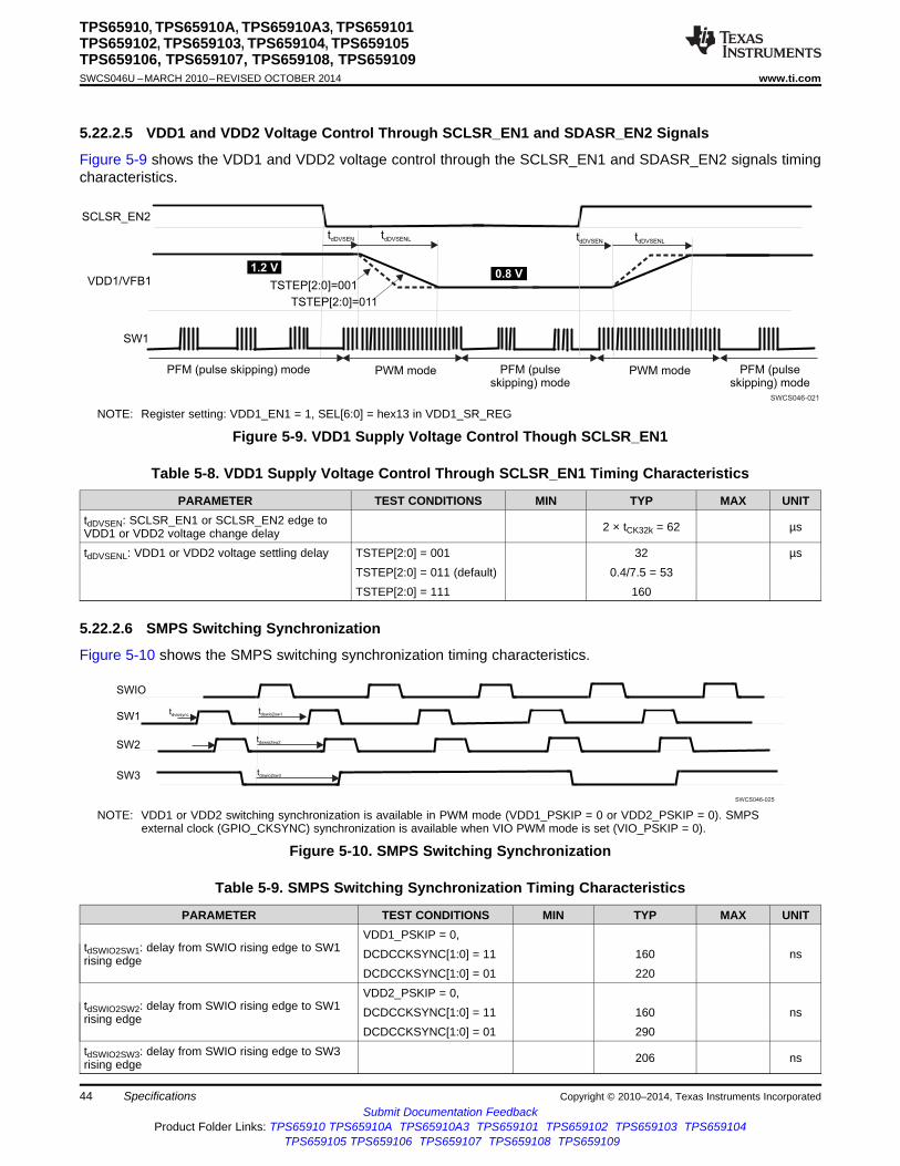
SWCS046-025
SW3
SW2
SWIO
SW1tdswio2sw1
tdswio2sw2
tdswio2sw3
tdviosync
1.2 V
SCLSR_EN2
PFM (pulseskipping) mode
SW1
VDD1/VFB10.8 V
PFM (pulseskipping) mode
PFM (pulse skipping) mode PWM mode PWM mode
tdDVSEN tdDVSENL tdDVSEN
TSTEP[2:0]=001
TSTEP[2:0]=011
tdDVSENL
SWCS046-021
TPS65910, TPS65910A, TPS65910A3, TPS659101TPS659102, TPS659103, TPS659104, TPS659105TPS659106, TPS659107, TPS659108, TPS659109SWCS046U –MARCH 2010–REVISED OCTOBER 2014 www.ti.com
5.22.2.5 VDD1 and VDD2 Voltage Control Through SCLSR_EN1 and SDASR_EN2 Signals
Figure 5-9 shows the VDD1 and VDD2 voltage control through the SCLSR_EN1 and SDASR_EN2 signals timingcharacteristics.
NOTE: Register setting: VDD1_EN1 = 1, SEL[6:0] = hex13 in VDD1_SR_REG
Figure 5-9. VDD1 Supply Voltage Control Though SCLSR_EN1
Table 5-8. VDD1 Supply Voltage Control Through SCLSR_EN1 Timing Characteristics
PARAMETER TEST CONDITIONS MIN TYP MAX UNITtdDVSEN: SCLSR_EN1 or SCLSR_EN2 edge to 2 × tCK32k = 62 µsVDD1 or VDD2 voltage change delaytdDVSENL: VDD1 or VDD2 voltage settling delay TSTEP[2:0] = 001 32 µs
TSTEP[2:0] = 011 (default) 0.4/7.5 = 53TSTEP[2:0] = 111 160
5.22.2.6 SMPS Switching Synchronization
Figure 5-10 shows the SMPS switching synchronization timing characteristics.
NOTE: VDD1 or VDD2 switching synchronization is available in PWM mode (VDD1_PSKIP = 0 or VDD2_PSKIP = 0). SMPSexternal clock (GPIO_CKSYNC) synchronization is available when VIO PWM mode is set (VIO_PSKIP = 0).
Figure 5-10. SMPS Switching Synchronization
Table 5-9. SMPS Switching Synchronization Timing Characteristics
PARAMETER TEST CONDITIONS MIN TYP MAX UNITVDD1_PSKIP = 0,
tdSWIO2SW1: delay from SWIO rising edge to SW1 DCDCCKSYNC[1:0] = 11 160 nsrising edgeDCDCCKSYNC[1:0] = 01 220VDD2_PSKIP = 0,
tdSWIO2SW2: delay from SWIO rising edge to SW1 DCDCCKSYNC[1:0] = 11 160 nsrising edgeDCDCCKSYNC[1:0] = 01 290
tdSWIO2SW3: delay from SWIO rising edge to SW3 206 nsrising edge
44 Specifications Copyright © 2010–2014, Texas Instruments IncorporatedSubmit Documentation Feedback
Product Folder Links: TPS65910 TPS65910A TPS65910A3 TPS659101 TPS659102 TPS659103 TPS659104TPS659105 TPS659106 TPS659107 TPS659108 TPS659109

TPS65910, TPS65910A, TPS65910A3, TPS659101TPS659102, TPS659103, TPS659104, TPS659105
TPS659106, TPS659107, TPS659108, TPS659109www.ti.com SWCS046U –MARCH 2010–REVISED OCTOBER 2014
6 Detailed Description
6.1 Power ReferenceThe bandgap voltage reference is filtered by using an external capacitor connected across the VREFoutput and the analog ground REFGND (see Section 5.3, Recommended Operating Conditions). TheVREF voltage is distributed and buffered inside the device.
6.2 Power SourcesThe power resources provided by the TPS65910 device include inductor-based switched mode powersupplies (SMPS) and linear low drop-out voltage regulators (LDOs). These supply resources provide therequired power to the external processor cores and external components, and to modules embedded inthe TPS65910 device.
Two of these SMPS have DVS capability SmartReflex Class 3 compatible. These SMPS provideindependent core voltage domains to the host processor. The remaining SMPS provides supply voltagefor the host processor I/Os.
Table 6-1 lists the power sources provided by the TPS65910 device.
Table 6-1. Power Sources
RESOURCE TYPE VOLTAGES POWERVIO SMPS 1.5 V / 1.8 V / 2.5 V / 3.3 V 1000 mA
VDD1 SMPS 0.6 ... 1.5 in 12.5-mV steps 1500 mAProgrammable multiplication factor: x2, x3
VDD2 SMPS 0.6 ... 1.5 in 12.5-mV steps 1500 mAProgrammable multiplication factor: x2, x3
VDD3 SMPS 5 V 100 mAVDIG1 LDO 1.2 V, 1.5 V, 1.8 V, 2.7 V 300 mAVDIG2 LDO 1 V, 1.1 V, 1.2 V, 1.8 V 300 mAVPLL LDO 1.0 V, 1.1 V, 1.8 V, 2.5 V 50 mAVDAC LDO 1.8 V, 2.6 V, 2.8 V, 2.85 V 150 mAVAUX1 LDO 1.8 V, 2.5 V, 2.8 V, 2.85 V 300 mAVAUX2 LDO 1.8 V, 2.8 V, 2.9 V, 3.3 V 150 mAVAUX33 LDO 1.8 V, 2.0 V, 2.8 V, 3.3 V 150 mAVMMC LDO 1.8 V, 2.8 V, 3.0 V, 3.3 V 300 mA
6.3 Embedded Power ControllerThe embedded power controller manages the state of the device and controls the power-up sequence.
6.3.1 State-MachineThe EPC supports the following states:
No supply: The main battery supply voltage is not high enough to power the VRTC regulator. A globalreset is asserted in this case. Everything on the device is off.
Backup: The main battery supply voltage is high enough to enable the VRTC domain but not enough toswitch on all the resources. In this state, the VRTC regulator is in backup mode and only the 32-Koscillator and RTC module are operating (if enabled). All other resources are off or under reset.
Off: The main battery supply voltage is high enough to start the power-up sequence but device power onis not enabled. All power supplies are in OFF state except VRTC.
Active: Device power-on enable conditions are met and regulated power supplies are on or can beenabled with full current capability.
Copyright © 2010–2014, Texas Instruments Incorporated Detailed Description 45Submit Documentation Feedback
Product Folder Links: TPS65910 TPS65910A TPS65910A3 TPS659101 TPS659102 TPS659103 TPS659104TPS659105 TPS659106 TPS659107 TPS659108 TPS659109

NO SUPPLY
OFF
ACTIVE
SLEEP
BackupMB or BB>VBNPR and
MB<VMBLO
MB and BB<VBNPR
MB<VMBLO
MB>VMBHI
POWER ONenabled andMB>VMBCH
MB>VMBHI
POWER ONdisabled
MB and BB<VBNPR
MB and BB<VBNPR
SLEEPenabled
POWER ONdisabled
MB: Main battery voltageBB: Backup battery voltage
MB<VMBLO
SLEEPdisabled
MB<VMBLO
SWCS046-011
PWRHOLD
DEV_ON
PWRON
INT1
PWRON_LP_IT
THERM_TS
DEV_OFF
DEV_OFF_RST
POWER ONenable
SLEEP
DEV_SLP
INT1
SLEEPenable
SLEEPSIG_POL
NRESPWRON
tDOINT
Pulsegenerator
tD
TPS65910, TPS65910A, TPS65910A3, TPS659101TPS659102, TPS659103, TPS659104, TPS659105TPS659106, TPS659107, TPS659108, TPS659109SWCS046U –MARCH 2010–REVISED OCTOBER 2014 www.ti.com
Sleep: Device SLEEP enable conditions are met and some selected regulated power supplies are in low-power mode.
Figure 6-1 shows the transitions of the state-machine.
Figure 6-1. Embedded Power Control State-Machine
46 Detailed Description Copyright © 2010–2014, Texas Instruments IncorporatedSubmit Documentation Feedback
Product Folder Links: TPS65910 TPS65910A TPS65910A3 TPS659101 TPS659102 TPS659103 TPS659104TPS659105 TPS659106 TPS659107 TPS659108 TPS659109

TPS65910, TPS65910A, TPS65910A3, TPS659101TPS659102, TPS659103, TPS659104, TPS659105
TPS659106, TPS659107, TPS659108, TPS659109www.ti.com SWCS046U –MARCH 2010–REVISED OCTOBER 2014
Device power-on enable conditions:If none of the device power-on disable conditions is met, the following conditions are available to turnon and/or maintain the ON state of the device:• PWRON signal low level.• Or PWRHOLD signal high level.• Or DEV_ON control bit set to 1 (default inactive).• Or interrupt flag active (default INT1 low) while the device is off (NRESPWRON = 0) generates a
power-on enable condition during a fixed delay (TDOINT1 pulse duration defined in Section 5.22.2,Power Control Timing).The power-on enable condition pulse occurs only if the interrupt status bit is initially low (noprevious identical interrupt pending in the status register).The Interrupt sources expected when the device is off are:• PWRON low-level interrupt (PWRON_IT = 1 in INT_STS_REG register)• PWRHOLD rising-edge interrupt (PWRHOLD_IT = 1 in INT_STS_REG register)The Interrupt sources expected if enabled when the device is off are:• RTC Alarm interrupt (RTC_ALARM_IT = 1 or RTC_PERIOD_IT = 1 in INT_STS_REG register)• First-time input voltage rising above VMBHI threshold (Boot mode or EEPROM dependent) and
input voltage > VMBCH threshold (VMBCH_IT = 1 in INT_STS_REG register).
GPIO_CKSYNC cannot be used to turn on the device (OFF-to-ACTIVE state transition), even if itsassociated interrupt is not masked, but can be used as an interrupt source to wake up the device fromSLEEP-to-ACTIVE state.
Device power-on disable conditions:• PWRON signal low level during more than the long-press delay: tdPWRONLP (can be disabled though
register programming). The interrupt corresponding to this condition is PWRON_LP_IT in theINT_STS_REG register.
• Or Die temperature has reached the thermal shutdown threshold.• Or DEV_OFF or DEV_OFF_RST control bit set to 1 (value of DEV_OFF is cleared when the device is
in OFF state).
Device SLEEP enable conditions:• SLEEP signal low level (default, or high level depending on the programmed polarity)• And DEV_SLP control bit set to 1• And interrupt flag inactive (default INT1 high): no nonmasked interrupt pending
The SLEEP state can be controlled by programming DEV_SLP and keeping the SLEEP signal in theactive polarity state, or it can be controlled through the SLEEP signal setting the DEV_SLP bit to 1 once,after device turn-on.
Copyright © 2010–2014, Texas Instruments Incorporated Detailed Description 47Submit Documentation Feedback
Product Folder Links: TPS65910 TPS65910A TPS65910A3 TPS659101 TPS659102 TPS659103 TPS659104TPS659105 TPS659106 TPS659107 TPS659108 TPS659109

TPS65910, TPS65910A, TPS65910A3, TPS659101TPS659102, TPS659103, TPS659104, TPS659105TPS659106, TPS659107, TPS659108, TPS659109SWCS046U –MARCH 2010–REVISED OCTOBER 2014 www.ti.com
6.3.2 Switch-On/-Off SequencesThe power sequence is the automated switching on of the device resources when an off-to-activetransition takes place.
The device supports three embedded power sequences selectable by the device BOOT pins.
BOOT0 BOOT1 Processor Supported0 0 AM3517, AM35051 0 OMAP3 Family, AM3715/03, DM3730/250 1 EEPROM sequence
Details of the boot sequence timing are given in Section 5.22.1. EEPROM sequences can be used forspecific power up sequence for corresponding application processor. For details of EEPROM sequencerefer to the user guides on the product folder: http://focus.ti.com/docs/prod/folders/print/tps65910.html.
6.3.3 Control Signals
6.3.3.1 SLEEP
When none of the device sleep-disable conditions are met, a falling edge (default, or rising edge,depending on the programmed polarity) of this signal causes an ACTIVE-to-SLEEP state transition of thedevice. A rising edge (default, or falling edge, depending on the programmed polarity) causes a transitionback to ACTIVE state. This input signal is level sensitive and no debouncing is applied.
While the device is in SLEEP state, predefined resources are automatically set in their low-power mode oroff. Resources can be kept in their active mode: (full-load capability), programming theSLEEP_KEEP_LDO_ON and the SLEEP_KEEP_RES_ON registers. These registers contain 1 bit perpower resource. If the bit is set to 1, then that resource stays in active mode when the device is in SLEEPstate. 32KCLKOUT is also included in the SLEEP_KEEP_RES_ON register and the 32-kHz clock output ismaintained in SLEEP state if the corresponding mask bit is set.
6.3.3.2 PWRHOLD
When none of the device power-on disable conditions are met, a rising edge of this signal causes an OFF-to-ACTIVE state transition of the device and a falling edge causes a transition back to OFF state.Typically, this signal is used to control the device in a slave configuration. It can be connected to theSYSEN output signal from other TPS659xx devices, or the NRESPWRON signal of another TPS65910device. This input signal is level sensitive and no debouncing is applied.
A rising edge of PWRHOLD is highlighted though an associated interrupt.
6.3.3.3 BOOT0/BOOT1
These signals determine which processor the device is working with and hence which power-up sequenceis needed. See Section 5.22.1 for more details. There is no debouncing on this input signal.
6.3.3.4 NRESPWRON
This signal is used as the reset to the processor. It is held low until the ACTIVE state is reached. SeeSection 5.22.2 to get detailed timing.
6.3.3.5 CLK32KOUT
This signal is the output of the 32K oscillator, which can be enabled or not during the power-on sequence,depending on the Boot mode. It can be enabled and disabled by register bit, during ACTIVE state of thedevice. CLK32KOUT output can also be enabled or not during SLEEP state of the device depending onthe SLEEPMASK register programming.
48 Detailed Description Copyright © 2010–2014, Texas Instruments IncorporatedSubmit Documentation Feedback
Product Folder Links: TPS65910 TPS65910A TPS65910A3 TPS659101 TPS659102 TPS659103 TPS659104TPS659105 TPS659106 TPS659107 TPS659108 TPS659109

TPS65910, TPS65910A, TPS65910A3, TPS659101TPS659102, TPS659103, TPS659104, TPS659105
TPS659106, TPS659107, TPS659108, TPS659109www.ti.com SWCS046U –MARCH 2010–REVISED OCTOBER 2014
6.3.3.6 PWRON
A falling edge on this signal causes after tdbPWRONF debouncing delay (defined in Figure 5-4 and Table 5-5)an OFF-to-ACTIVE state or SLEEP-to-ACTIVE state transition of the device and makes the correspondinginterrupt (PWRON_IT) active. The PWRON input is connected to an external push-button. The built-indebouncing time defines a minimum button press duration that is required for button press detection. Anybutton press duration which is lower than this value is ignored, considered an accidental touch.
After an OFF-to-ACTIVE state transition, the PMIC maintains ACTIVE during tdOINT delay, if the button isreleased. After this delay if none of the device enabling conditions is set by the processor supplied, thePMIC automatically turns off. If the button is not released, the PMIC maintains ACTIVE up to tdPWRONLPTO,because PWRON low is a device enabling condition. After a SLEEP-to-ACTIVE state transition, the PMICmaintains ACTIVE as long as an interrupt is pending.
If the device is already in ACTIVE state, a PWRON low level makes the corresponding interrupt(PWRON_IT) active.
When the PMIC is in ACTIVE mode, if the button is pressed for longer time than tdPWRONLP, the PMICgenerates the PWON_LP_IT interrupt. If the processor does not acknowledge the long press interruptwithin a period of tdPWRONLPTO – tdPWRONLP, the PMIC goes to OFF mode and shuts down the DCDCs andLDOs.
6.3.3.7 INT1
INT1 signal (default active low) warns the host processor of any event that occurred on the TPS65910device. The host processor can then poll the interrupt from the interrupt status register through I2C toidentify the interrupt source. A low level (default setting) indicates an active interrupt, highlighted in theINT_STS_REG register. The polarity of INT1 can be set by programming the IT_POL control bit.
Any (not masked or masked) interrupt detection causes a POWER ON enable condition during a fixeddelay tDOINT1 (only) when the device is in OFF state (when NRESPWON signal is low). Any (not masked)interrupt detection is causing a device wakeup from SLEEP state up to acknowledge of the pendinginterrupt. Any of the interrupt sources can be masked by programming the INT_MSK_REG register. Whenan interrupt is masked, its corresponding interrupt status bit is still updated, but the INT1 flag is notactivated.
Interrupt source masking can be used to mask a device switch-on event. Because interrupt flag active is aPOWER ON enable condition during tDOINT1 delay, any interrupt not masked must be cleared to allow turnoff of the device after the tDOINT1 POWER ON enable pulse duration.. See section: Interrupts, for interruptsources definition.
6.3.3.8 SDASR_EN2 and SCLSR_EN1
SDASR_EN2 and SCLSR_EN1 are the data and clock signals of the serial control interface (SR-I2C)dedicated to SmartReflex applications. These signals can also be programmed to be used as enablesignals of one or several supplies, when the device is on (NRESPWRON high). A resource assigned toSDASR_EN2 or SCLSR_EN1 control automatically disables the serial control interface.
Programming EN1_LDO_ASS_REG, EN2_LDO_REG, and SLEEP_KEEP_LDO_ON_REG registers:SCLSR_EN1 and SDASR_EN2 signals can be used to control the turn on/off or sleep state of any LDOtype supplies.
Programming EN1_SMPS_ASS_REG, EN2_SMPS_ASS_REG, and SLEEP_KEEP_RES_ON registers:SCLSR_EN1 and SDASR_EN2 signals can be used to control the turn on/off or low-power state (PFMmode) of SMPS type supplies.
SDASR_EN2 and SCLSR_EN1 can be used to set output voltage of VDD1 and VDD2 SMPS from a roofto a floor value, preprogrammed in the VDD1_OP_REG, VDD2_OP_REG, and teh VDD1_SR_REG,VDD2_SR_REG registers. Tun-off of VDD1 and VDD2 can also be programmed either inVDD1_OP_REG, VDD2_OP_REG or in VDD1_SR_REG, VDD2_SR_REG registers.
Copyright © 2010–2014, Texas Instruments Incorporated Detailed Description 49Submit Documentation Feedback
Product Folder Links: TPS65910 TPS65910A TPS65910A3 TPS659101 TPS659102 TPS659103 TPS659104TPS659105 TPS659106 TPS659107 TPS659108 TPS659109

TPS65910, TPS65910A, TPS65910A3, TPS659101TPS659102, TPS659103, TPS659104, TPS659105TPS659106, TPS659107, TPS659108, TPS659109SWCS046U –MARCH 2010–REVISED OCTOBER 2014 www.ti.com
When a supply is controlled through SCLSR_EN1 or SCLSR_EN2 signals, its state is no longer driven bythe device SLEEP state.
6.3.3.9 GPIO_CKSYNC
GPIO_CKSYNC is a configurable open-drain digital I/O: directivity, debouncing delay and internal pullupcan be programmed in the GPIO0_REG register. GPIO_CKSYNC cannot be used to turn on the device(OFF-to-ACTIVE state transition), even if its associated interrupt is not masked, but can be used as aninterrupt source to wake up the device from SLEEP-to-ACTIVE state.
Programming DCDCCKEXT = 1, VDD1, VDD2, VIO, and VDD3 DC-DC switching can be synchronizedusing a 3-MHz clock set though the GPIO_CKSYNC pin.
6.3.4 Dynamic Voltage Frequency Scaling and Adaptive Voltage Scaling OperationDynamic voltage frequency scaling (DVFS) operation: a supply voltage value corresponding to a targetedfrequency of the digital core supplied is programmed in VDD1_OP_REG or VDD2_OP_REG registers.
The slew rate of the voltage supply reaching a new VDD1_OP_REG or VDD2_OP_REG programmedvalue is limited to 12.5 mV/µs, fixed value. Adaptative voltage scaling (AVS) operation: a supply voltagevalue corresponding to a supply voltage adjustment is programmed in VDD1_SR_REG orVDD2_SR_REG registers. The supply voltage is then intended to be tuned by the digital core supplied,based its performance self-evaluation. The slew rate of VDD1 or VDD2 voltage supply reaching a newprogrammed value is programmable though the VDD1_REG or VDD2_REG register, respectively.
A serial control interface (SR-I2C) is dedicated to SmartReflex applications such as DVFS and class 3AVS, and thus gives access to the VDD1_OP_REG, VDD1_SR_REG, and VDD2_OP_REG,VDD2_SR_REG register.
A general-purpose serial control interface (CTL-I2C) also gives access to these registers, ifSR_CTL_I2C_SEL control bit is set to 1 in the DEVCTRL_REG register (default inactive).
Both control interfaces are compliant with HS-I2C specification (100 kbps, 400 kbps, or 3.4 Mbps).
Figure 6-2 shows an example of a SmartReflex operation. To optimize power efficiency, the voltagedomains of the host processor uses the DVFS and AVS features provided by SmartReflex.
50 Detailed Description Copyright © 2010–2014, Texas Instruments IncorporatedSubmit Documentation Feedback
Product Folder Links: TPS65910 TPS65910A TPS65910A3 TPS659101 TPS659102 TPS659103 TPS659104TPS659105 TPS659106 TPS659107 TPS659108 TPS659109

OPP1
OPP2
OPP3
OPP4
OPP5
OPP Change start
OPP Change end
Coarse steps (DVFS) Fine steps (AVS)
SWCS046-012
TSR TI2C TSMPS TSR TI2C TSMPS TSR TI2C TSMPS TSR TI2C TSMPS
TPS65910, TPS65910A, TPS65910A3, TPS659101TPS659102, TPS659103, TPS659104, TPS659105
TPS659106, TPS659107, TPS659108, TPS659109www.ti.com SWCS046U –MARCH 2010–REVISED OCTOBER 2014
(1) TSR: Time used by the SmartReflex controller(2) TI2C: Time used for data transfer through the I2C interface(3) TSMPS: Time required by the SMPS to converge to new voltage value
Figure 6-2. SmartReflex Operation Example
Copyright © 2010–2014, Texas Instruments Incorporated Detailed Description 51Submit Documentation Feedback
Product Folder Links: TPS65910 TPS65910A TPS65910A3 TPS659101 TPS659102 TPS659103 TPS659104TPS659105 TPS659106 TPS659107 TPS659108 TPS659109

Biasing
and
amplitude
control
32 kHz todigital block
VRTC
OSC32KOUTOSC32KIN
SWCS046-013
REFGND
Q
Coscin Coscout
TPS65910, TPS65910A, TPS65910A3, TPS659101TPS659102, TPS659103, TPS659104, TPS659105TPS659106, TPS659107, TPS659108, TPS659109SWCS046U –MARCH 2010–REVISED OCTOBER 2014 www.ti.com
6.4 32-kHz RTC ClockThe TPS65910 device can provide a 32-kHz clock to the platform through the CLK32KOUT output, thesource of this 32-kHz clock can be:• 32-kHz crystal connected from OSC32IN to OSC32KOUT pins• A square-wave 32-kHz clock signal applied to OSC32IN input (OSC32KOUT kept floating).• Internal 32-kHz RC oscillator, to reduce the BOM, if an accurate clock is not needed by the system.
Default selection of a 32-kHz RC oscillator versus 32-kHz crystal oscillator or external square-wave 32-kHz clock depends on the Boot mode or device version (EEPROM programming):• BOOT1 = 0, BOOT0 = 1: quartz oscillator or external square wave 32-kHz clock default• BOOT1 = 0, BOOT0 = 0: 32-kHz RC oscillator default
Switching from the 32-kHz RC oscillator to the 32-kHz crystal oscillator or external square-wave 32-kHzclock can also be programmed though DEVCTRL_REG register, taking benefit of the shorter turn-on timeof the internal RC oscillator.
Switching from the 32-kHz crystal oscillator or external square-wave clock to the RC oscillator is notsupported.
Figure 6-3. Crystal Oscillator 32-kHz Clock
52 Detailed Description Copyright © 2010–2014, Texas Instruments IncorporatedSubmit Documentation Feedback
Product Folder Links: TPS65910 TPS65910A TPS65910A3 TPS659101 TPS659102 TPS659103 TPS659104TPS659105 TPS659106 TPS659107 TPS659108 TPS659109
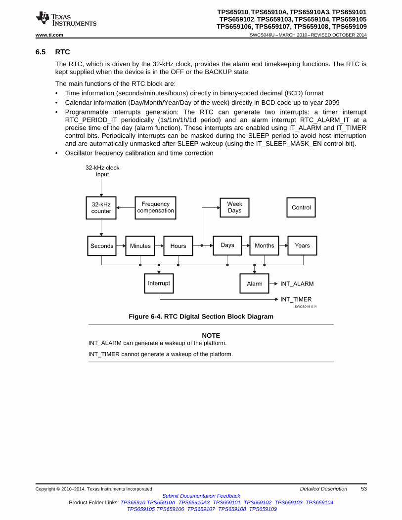
Hours
32-kHz clockinput
INT_ALARM
INT_TIMER
Seconds
Interrupt
Minutes
WeekDays
Days Months Years
Control
Alarm
Frequencycompensation
32-kHzcounter
SWCS046-014
TPS65910, TPS65910A, TPS65910A3, TPS659101TPS659102, TPS659103, TPS659104, TPS659105
TPS659106, TPS659107, TPS659108, TPS659109www.ti.com SWCS046U –MARCH 2010–REVISED OCTOBER 2014
6.5 RTCThe RTC, which is driven by the 32-kHz clock, provides the alarm and timekeeping functions. The RTC iskept supplied when the device is in the OFF or the BACKUP state.
The main functions of the RTC block are:• Time information (seconds/minutes/hours) directly in binary-coded decimal (BCD) format• Calendar information (Day/Month/Year/Day of the week) directly in BCD code up to year 2099• Programmable interrupts generation: The RTC can generate two interrupts: a timer interrupt
RTC_PERIOD_IT periodically (1s/1m/1h/1d period) and an alarm interrupt RTC_ALARM_IT at aprecise time of the day (alarm function). These interrupts are enabled using IT_ALARM and IT_TIMERcontrol bits. Periodically interrupts can be masked during the SLEEP period to avoid host interruptionand are automatically unmasked after SLEEP wakeup (using the IT_SLEEP_MASK_EN control bit).
• Oscillator frequency calibration and time correction
Figure 6-4. RTC Digital Section Block Diagram
NOTEINT_ALARM can generate a wakeup of the platform.
INT_TIMER cannot generate a wakeup of the platform.
Copyright © 2010–2014, Texas Instruments Incorporated Detailed Description 53Submit Documentation Feedback
Product Folder Links: TPS65910 TPS65910A TPS65910A3 TPS659101 TPS659102 TPS659103 TPS659104TPS659105 TPS659106 TPS659107 TPS659108 TPS659109

TPS65910, TPS65910A, TPS65910A3, TPS659101TPS659102, TPS659103, TPS659104, TPS659105TPS659106, TPS659107, TPS659108, TPS659109SWCS046U –MARCH 2010–REVISED OCTOBER 2014 www.ti.com
6.5.1 Time Calendar RegistersAll the time and calendar information are available in these dedicated registers, called TC registers.Values of the TC registers are written in BCD format.1. Year data ranges from 00 to 99
– Leap year = Year divisible by four (2000, 2004, 2008, 2012...)– Common year = other years
2. Month data ranges from 01 to 123. Day value ranges from:
– 1 to 31 when months are 1, 3, 5, 7, 8, 10, 12– 1 to 30 when months are 4, 6, 9, 11– 1 to 29 when month is 2 and year is a leap year– 1 to 28 when month is 2 and year is a common year
4. Week value ranges from 0 to 65. Hour value ranges from 00 to 23 in 24-hour mode and ranges from 1 to 12 in AM/PM mode6. Minutes value ranges from 0 to 597. Seconds value ranges from 0 to 59
To modify the current time, software writes the new time into TC registers to fix the time/calendarinformation. The DBB can write into TC registers without stopping the RTC. In addition, software can stopthe RTC by clearing the STOP_RTC bit of the control register and check the RUN bit of the status to besure that the RTC is frozen. Then update TC values, and then restart the RTC by setting the STOP_RTCbit.
Example: Time is 10H54M36S PM (PM_AM mode set), 2008 September 5, previous register values are:
Register ValueSECONDS_REG 0x36MINUTES_REG 0x54HOURS_REG 0x90DAYS_REG 0x05
MONTHS_REG 0x09YEARS_REG 0x08
The user can round to the closest minute, by setting the ROUND_30S register bit. TC values are set tothe closest minute value at the next second. The ROUND_30S bit is automatically cleared when therounding time is performed.
Example:• If current time is 10H59M45S, a round operation changes time to 11H00M00S.• if current time is 10H59M29S, a round operation changes time to 10H59M00S.
6.5.2 General RegistersSoftware can access the RTC_STATUS_REG and RTC_CTRL_REG registers at any time (except for theRTC_CTRL_REG[5] bit, which must be changed only when the RTC is stopped).
6.5.3 Compensation RegistersThe RTC_COMP_MSB_REG and RTC_COMP_LSB_REG registers must respect the available accessperiod. These registers must be updated before each compensation process. For example, software canload the compensation value into these registers after each hour event, during an available access period.
54 Detailed Description Copyright © 2010–2014, Texas Instruments IncorporatedSubmit Documentation Feedback
Product Folder Links: TPS65910 TPS65910A TPS65910A3 TPS659101 TPS659102 TPS659103 TPS659104TPS659105 TPS659106 TPS659107 TPS659108 TPS659109

3 64
59 0 158 2Seconds 59 0 158 2
Hours
3 4Hours
59 0 1Seconds
Compensation event
Compensation event
swcs046-015
TPS65910, TPS65910A, TPS65910A3, TPS659101TPS659102, TPS659103, TPS659104, TPS659105
TPS659106, TPS659107, TPS659108, TPS659109www.ti.com SWCS046U –MARCH 2010–REVISED OCTOBER 2014
Figure 6-5. RTC Compensation Scheduling
This drift can be balanced to compensate for any inaccuracy of the 32-kHz oscillator. Software mustcalibrate the oscillator frequency, calculate the drift compensation versus one time hour period; and thenload the compensation registers with the drift compensation value. Indeed, if the AUTO_COMP_EN bit inthe RTC_CTRL_REG is enabled, the value of COMP_REG (in twos-complement) is added to the RTC 32-kHz counter at each hour and one second. When COMP_REG is added to the RTC 32-kHz counter, theduration of the current second becomes (32768 - COMP_REG)/32768s; so, the RTC can be compensatedwith a 1/32768 s/hour time unit accuracy.
NOTEThe compensation is considered once written into the registers.
6.6 Backup Battery ManagementThe device includes a back-up battery switch connecting the VRTC regulator input to a main battery(VCC7) or to a back-up battery (VBACKUP), depending on the batteries voltage value.
The VRTC supply can then be maintained during a BACKUP state as far as the input voltage is highenough (>VBNPR threshold). Below the VBNPR voltage threshold the digital core of the device is setunder reset by internal signal POR (Power-on Reset).
The back-up domain functions which are always supplied from VRTC comprehend:• The internal 32-kHz oscillator• Backup registers
The back-up battery can be charged from the main battery through an embedded charger. The back-upbattery charge voltage and enable is controlled through BBCH_REG register programming. This registercontent is maintained during the device Backup state.
Hence enabled the back-up battery charge is maintained as far as the main battery voltage is higher thanthe VMBLO threshold and the back-up battery voltage.
Copyright © 2010–2014, Texas Instruments Incorporated Detailed Description 55Submit Documentation Feedback
Product Folder Links: TPS65910 TPS65910A TPS65910A3 TPS659101 TPS659102 TPS659103 TPS659104TPS659105 TPS659106 TPS659107 TPS659108 TPS659109

TPS65910, TPS65910A, TPS65910A3, TPS659101TPS659102, TPS659103, TPS659104, TPS659105TPS659106, TPS659107, TPS659108, TPS659109SWCS046U –MARCH 2010–REVISED OCTOBER 2014 www.ti.com
6.7 Backup RegistersAs part of the RTC the device contains five 8-bit registers which can be used for storage by the applicationfirmware when the external host is powered down. These registers retain their content as long as theVRTC is active.
6.8 I2C InterfaceA general-purpose serial control interface (CTL-I2C) allows read and write access to the configurationregisters of all resources of the system.
A second serial control interface (SR-I2C) is dedicated to SmartReflex applications such as DVFS or AVS.
Both control interfaces are compliant with HS-I2C specification.
These interfaces support the standard slave mode (100 Kbps), Fast mode (400 Kbps), and high-speedmode (3.4 Mbps). The general-purpose I2C module using one slave hard-coded address (ID1 = 2Dh). TheSmartReflex I2C module uses one slave hard-coded address (ID0 = 12h). The master mode is notsupported.
Addressing: Seven-bit mode addressing device
They do not support the following features:• 10-bit addressing• General call
6.9 Thermal Monitoring and ShutdownA thermal protection module monitors the junction temperature of the device versus two thresholds:• Hot-die temperature threshold• Thermal shutdown temperature threshold
When the hot-die temperature threshold is reached an interrupt is sent to software to close the noncriticalrunning tasks.
When the thermal shutdown temperature threshold is reached, the TPS65910 device is set under resetand a transition to OFF state is initiated. Then the power-on enable conditions of the device is notconsidered until the die temperature has decreased below the hot-die threshold. An hysteresis is appliedto the hot-die and shutdown threshold, when detecting a falling edge of temperature, and both detectionare debounced to avoid any parasitic detection. The TPS65910 device allows programming of four hot-dietemperature thresholds to increase the flexibility of the system.
By default, the thermal protection is enabled in ACTIVE state, but can be disabled through programmingregister THERM_REG. The thermal protection can be enabled in SLEEP state programming registerSLEEP_KEEP_RES_ON. The thermal protection is automatically enabled during an OFF-to-ACTIVE statetransition and is kept enabled in OFF state after a switch-off sequence caused by a thermal shutdownevent. Transition to OFF state sequence caused by a thermal shutdown event is highlighted in theINT_STS_REG status register. Recovery from this OFF state is initiated (switch-on sequence) when thedie temperature falls below the hot-die temperature threshold.
Hot-die and thermal shutdown temperature threshold detections state can be monitored or masked byreading or programming the THERM_REG register. Hot-die interrupt can be masked by programming theINT_MSK_REG register.
56 Detailed Description Copyright © 2010–2014, Texas Instruments IncorporatedSubmit Documentation Feedback
Product Folder Links: TPS65910 TPS65910A TPS65910A3 TPS659101 TPS659102 TPS659103 TPS659104TPS659105 TPS659106 TPS659107 TPS659108 TPS659109

TPS65910, TPS65910A, TPS65910A3, TPS659101TPS659102, TPS659103, TPS659104, TPS659105
TPS659106, TPS659107, TPS659108, TPS659109www.ti.com SWCS046U –MARCH 2010–REVISED OCTOBER 2014
6.10 Interrupts
Table 6-2. Interrupt Sources
Interrupt DescriptionRTC_ALARM_IT RTC alarm event: Occurs at programmed determinate date and time
(running in ACTIVE, OFF, and SLEEP state, default inactive)RTC periodic event: Occurs at programmed regular period of time (every second or minute)RTC_PERIOD_IT (running in ACTIVE, OFF, and SLEEP state, default inactive)The embedded thermal monitoring module has detected a die temperature above the hot-dieHOT_DIE_IT detection threshold (running in ACTIVE and SLEEP state)Level sensitive interrupt.
PWRHOLD_IT PWRHOLD signal rising edgePWRON is low during more than the long-press delay: tdPWRONLP (can be disable thoughPWRON_LP_IT register programming).PWRON is low while the device is on (running in ACTIVE and SLEEP state) or PWON wasPWRON_IT low while the device was off (causing a device turn-on). Level-sensitive interruptThe battery voltage rise above the VMBHI threshold: NOSUPPLY to Off or Backup-to-Offdevice states transition (first battery plug or battery voltage bounce detection). This interruptVMBHI_IT source can be disabled through EEPROM programming (VMBHI_IT_DIS). Edge-sensitiveinterruptThe battery voltage falls down below the VMBDCH threshold(running in ACTIVE and SLEEPVMBDCH_IT state, if enabled programming VMBCH_VSEL). Edge-sensitive interrupt
GPIO0_R_IT GPIO_CKSYNC rising-edge detection (available in ACTIVE and SLEEP state)GPIO0_F_IT GPIO_CKSYNC falling-edge detection (available in ACTIVE and SLEEP state)
INT1 signal (active low) warns the host processor of any event that occurred on the TPS65910 device.The host processor can then poll the interrupt from the interrupt status register via I2C to identify theinterrupt source. Each interrupt source can be individually masked via the interrupt mask register.
6.11 Package DescriptionThe following are the package descriptions of the TPS65910 PMU devices:• Package type:
Package TPS65910Type RSL QFN-N48Size (mm) 6x6Substrate layers 1 layerPitch ball array (mm) 0.4 mmViP (via-in-pad) NoNumber of balls 48Thickness (mm) (max height including balls) 1Others Green, ROHS-compliant
• Moisture sensitivity level target: JEDEC MSL3 at 260°C
Copyright © 2010–2014, Texas Instruments Incorporated Detailed Description 57Submit Documentation Feedback
Product Folder Links: TPS65910 TPS65910A TPS65910A3 TPS659101 TPS659102 TPS659103 TPS659104TPS659105 TPS659106 TPS659107 TPS659108 TPS659109

TPS65910, TPS65910A, TPS65910A3, TPS659101TPS659102, TPS659103, TPS659104, TPS659105TPS659106, TPS659107, TPS659108, TPS659109SWCS046U –MARCH 2010–REVISED OCTOBER 2014 www.ti.com
6.12 Functional Registers
6.12.1 TPS65910_FUNC_REG Registers Mapping Summary
Table 6-3. TPS65910_FUNC_REG Register Summary
Register Name Type Register Width (Bits) Register Reset Address OffsetSECONDS_REG RW 8 0x00 0x00MINUTES_REG RW 8 0x00 0x01HOURS_REG RW 8 0x00 0x02DAYS_REG RW 8 0x01 0x03MONTHS_REG RW 8 0x01 0x04YEARS_REG RW 8 0x00 0x05WEEKS_REG RW 8 0x00 0x06ALARM_SECONDS_REG RW 8 0x00 0x08ALARM_MINUTES_REG RW 8 0x00 0x09ALARM_HOURS_REG RW 8 0x00 0x0AALARM_DAYS_REG RW 8 0x01 0x0BALARM_MONTHS_REG RW 8 0x01 0x0CALARM_YEARS_REG RW 8 0x00 0x0DRTC_CTRL_REG RW 8 0x00 0x10RTC_STATUS_REG RW 8 0x80 0x11RTC_INTERRUPTS_REG RW 8 0x00 0x12RTC_COMP_LSB_REG RW 8 0x00 0x13RTC_COMP_MSB_REG RW 8 0x00 0x14RTC_RES_PROG_REG RW 8 0x27 0x15RTC_RESET_STATUS_REG RW 8 0x00 0x16BCK1_REG RW 8 0x00 0x17BCK2_REG RW 8 0x00 0x18BCK3_REG RW 8 0x00 0x19BCK4_REG RW 8 0x00 0x1ABCK5_REG RW 8 0x00 0x1BPUADEN_REG RW 8 0x9F 0x1CREF_REG RW 8 0x01 0x1DVRTC_REG RW 8 0x01 0x1EVIO_REG RW 8 0x00 0x20VDD1_REG RW 8 0x0C 0x21VDD1_OP_REG RW 8 0x00 0x22VDD1_SR_REG RW 8 0x00 0x23VDD2_REG RW 8 0x04 0x24VDD2_OP_REG RW 8 0x00 0x25VDD2_SR_REG RW 8 0x00 0x26VDD3_REG RW 8 0x04 0x27VDIG1_REG RW 8 0x00 0x30VDIG2_REG RW 8 0x00 0x31VAUX1_REG RW 8 0x00 0x32VAUX2_REG RW 8 0x00 0x33VAUX33_REG RW 8 0x00 0x34VMMC_REG RW 8 0x00 0x35VPLL_REG RW 8 0x00 0x36VDAC_REG RW 8 0x00 0x37
58 Detailed Description Copyright © 2010–2014, Texas Instruments IncorporatedSubmit Documentation Feedback
Product Folder Links: TPS65910 TPS65910A TPS65910A3 TPS659101 TPS659102 TPS659103 TPS659104TPS659105 TPS659106 TPS659107 TPS659108 TPS659109

TPS65910, TPS65910A, TPS65910A3, TPS659101TPS659102, TPS659103, TPS659104, TPS659105
TPS659106, TPS659107, TPS659108, TPS659109www.ti.com SWCS046U –MARCH 2010–REVISED OCTOBER 2014
Table 6-3. TPS65910_FUNC_REG Register Summary (continued)Register Name Type Register Width (Bits) Register Reset Address OffsetTHERM_REG RW 8 0x0D 0x38BBCH_REG RW 8 0x00 0x39DCDCCTRL_REG RW 8 0x3B 0x3EDEVCTRL_REG RW 8 0x40 0x3FDEVCTRL2_REG RW 8 0x34 0x40SLEEP_KEEP_LDO_ON_REG RW 8 0x00 0x41SLEEP_KEEP_RES_ON_REG RW 8 0x00 0x42SLEEP_SET_LDO_OFF_REG RW 8 0x00 0x43SLEEP_SET_RES_OFF_REG RW 8 0x00 0x44EN1_LDO_ASS_REG RW 8 0x00 0x45EN1_SMPS_ASS_REG RW 8 0x00 0x46EN2_LDO_ASS_REG RW 8 0x00 0x47EN2_SMPS_ASS_REG RW 8 0x00 0x48RESERVED RW 8 0x00 0x49RESERVED RW 8 0x00 0x4AINT_STS_REG RW 8 0x00 0x50INT_MSK_REG RW 8 0x02 0x51INT_STS2_REG RW 8 0x00 0x52INT_MSK2_REG RW 8 0x00 0x53GPIO0_REG RW 8 0x0A 0x60JTAGVERNUM_REG RO 8 0x00 0x80
Copyright © 2010–2014, Texas Instruments Incorporated Detailed Description 59Submit Documentation Feedback
Product Folder Links: TPS65910 TPS65910A TPS65910A3 TPS659101 TPS659102 TPS659103 TPS659104TPS659105 TPS659106 TPS659107 TPS659108 TPS659109

TPS65910, TPS65910A, TPS65910A3, TPS659101TPS659102, TPS659103, TPS659104, TPS659105TPS659106, TPS659107, TPS659108, TPS659109SWCS046U –MARCH 2010–REVISED OCTOBER 2014 www.ti.com
6.12.2 TPS65910_FUNC_REG Register Descriptions
Table 6-4. SECONDS_REG
Address Offset 0x00Physical Address InstanceDescription RTC register for secondsType RW
7 6 5 4 3 2 1 0Reserved SEC1 SEC0
Bits Field Name Description Type Reset7 Reserved Reserved bit RO 0
R returns0s
6:4 SEC1 Second digit of seconds (range is 0 up to 5) RW 0x03:0 SEC0 First digit of seconds (range is 0 up to 9) RW 0x0
Table 6-5. MINUTES_REG
Address Offset 0x01Physical Address InstanceDescription RTC register for minutesType RW
7 6 5 4 3 2 1 0Reserved MIN1 MIN0
Bits Field Name Description Type Reset7 Reserved Reserved bit RO 0
R returns0s
6:4 MIN1 Second digit of minutes (range is 0 up to 5) RW 0x03:0 MIN0 First digit of minutes (range is 0 up to 9) RW 0x0
Table 6-6. HOURS_REG
Address Offset 0x02Physical Address InstanceDescription RTC register for hoursType RW
7 6 5 4 3 2 1 0PM_NAM Reserved HOUR1 HOUR0
Bits Field Name Description Type Reset7 PM_NAM Only used in PM_AM mode (otherwise it is set to 0) RW 0
0 is AM1 is PM
6 Reserved Reserved bit RO 0R returns
0s5:4 HOUR1 Second digit of hours (range is 0 up to 2) RW 0x03:0 HOUR0 First digit of hours (range is 0 up to 9) RW 0x0
60 Detailed Description Copyright © 2010–2014, Texas Instruments IncorporatedSubmit Documentation Feedback
Product Folder Links: TPS65910 TPS65910A TPS65910A3 TPS659101 TPS659102 TPS659103 TPS659104TPS659105 TPS659106 TPS659107 TPS659108 TPS659109

TPS65910, TPS65910A, TPS65910A3, TPS659101TPS659102, TPS659103, TPS659104, TPS659105
TPS659106, TPS659107, TPS659108, TPS659109www.ti.com SWCS046U –MARCH 2010–REVISED OCTOBER 2014
Table 6-7. DAYS_REG
Address Offset 0x03Physical Address InstanceDescription RTC register for daysType RW
7 6 5 4 3 2 1 0Reserved DAY1 DAY0
Bits Field Name Description Type Reset7:6 Reserved Reserved bit RO 0x0
R returns0s
5:4 DAY1 Second digit of days (range is 0 up to 3) RW 0x03:0 DAY0 First digit of days (range is 0 up to 9) RW 0x1
Table 6-8. MONTHS_REG
Address Offset 0x04Physical Address InstanceDescription RTC register for monthsType RW
7 6 5 4 3 2 1 0Reserved MONTH1 MONTH0
Bits Field Name Description Type Reset7:5 Reserved Reserved bit RO 0x0
R returns0s
4 MONTH1 Second digit of months (range is 0 up to 1) RW 03:0 MONTH0 First digit of months (range is 0 up to 9) RW 0x1
Table 6-9. YEARS_REG
Address Offset 0x05Physical Address InstanceDescription RTC register for day of the weekType RW
7 6 5 4 3 2 1 0YEAR1 YEAR0
Bits Field Name Description Type Reset7:4 YEAR1 Second digit of years (range is 0 up to 9) RW 0x03:0 YEAR0 First digit of years (range is 0 up to 9) RW 0x0
Copyright © 2010–2014, Texas Instruments Incorporated Detailed Description 61Submit Documentation Feedback
Product Folder Links: TPS65910 TPS65910A TPS65910A3 TPS659101 TPS659102 TPS659103 TPS659104TPS659105 TPS659106 TPS659107 TPS659108 TPS659109

TPS65910, TPS65910A, TPS65910A3, TPS659101TPS659102, TPS659103, TPS659104, TPS659105TPS659106, TPS659107, TPS659108, TPS659109SWCS046U –MARCH 2010–REVISED OCTOBER 2014 www.ti.com
Table 6-10. WEEKS_REG
Address Offset 0x06Physical Address InstanceDescription RTC register for day of the weekType RW
7 6 5 4 3 2 1 0Reserved WEEK
Bits Field Name Description Type Reset7:3 Reserved Reserved bit RO 0x00
R returns0s
2:0 WEEK First digit of day of the week (range is 0 up to 6) RW 0
Table 6-11. ALARM_SECONDS_REG
Address Offset 0x08Physical Address InstanceDescription RTC register for alarm programming for secondsType RW
7 6 5 4 3 2 1 0Reserved ALARM_SEC1 ALARM_SEC0
Bits Field Name Description Type Reset7 Reserved Reserved bit RO 0
R returns0s
6:4 ALARM_SEC1 Second digit of alarm programming for seconds (range is 0 up to 5) RW 0x03:0 ALARM_SEC0 First digit of alarm programming for seconds (range is 0 up to 9) RW 0x0
Table 6-12. ALARM_MINUTES_REG
Address Offset 0x09Physical Address InstanceDescription RTC register for alarm programming for minutesType RW
7 6 5 4 3 2 1 0Reserved ALARM_MIN1 ALARM_MIN0
Bits Field Name Description Type Reset7 Reserved Reserved bit RO 0
R returns0s
6:4 ALARM_MIN1 Second digit of alarm programming for minutes (range is 0 up to 5) RW 0x03:0 ALARM_MIN0 First digit of alarm programming for minutes (range is 0 up to 9) RW 0x0
62 Detailed Description Copyright © 2010–2014, Texas Instruments IncorporatedSubmit Documentation Feedback
Product Folder Links: TPS65910 TPS65910A TPS65910A3 TPS659101 TPS659102 TPS659103 TPS659104TPS659105 TPS659106 TPS659107 TPS659108 TPS659109

TPS65910, TPS65910A, TPS65910A3, TPS659101TPS659102, TPS659103, TPS659104, TPS659105
TPS659106, TPS659107, TPS659108, TPS659109www.ti.com SWCS046U –MARCH 2010–REVISED OCTOBER 2014
Table 6-13. ALARM_HOURS_REG
Address Offset 0x0APhysical Address InstanceDescription RTC register for alarm programming for hoursType RW
7 6 5 4 3 2 1 0ALARM_PM_N Reserved ALARM_HOUR1 ALARM_HOUR0AM
Bits Field Name Description Type Reset7 ALARM_PM_NAM Only used in PM_AM mode for alarm programming (otherwise it is set to RW 0
0)0 is AM1 is PM
6 Reserved Reserved bit RO 0R returns
0s5:4 ALARM_HOUR1 Second digit of alarm programming for hours (range is 0 up to 2) RW 0x03:0 ALARM_HOUR0 First digit of alarm programming for hours (range is 0 up to 9) RW 0x0
Table 6-14. ALARM_DAYS_REG
Address Offset 0x0BPhysical Address InstanceDescription RTC register for alarm programming for daysType RW
7 6 5 4 3 2 1 0Reserved ALARM_DAY1 ALARM_DAY0
Bits Field Name Description Type Reset7:6 Reserved Reserved bit RO 0x0
R Special5:4 ALARM_DAY1 Second digit of alarm programming for days (range is 0 up to 3) RW 0x03:0 ALARM_DAY0 First digit of alarm programming for days (range is 0 up to 9) RW 0x1
Table 6-15. ALARM_MONTHS_REG
Address Offset 0x0CPhysical Address InstanceDescription RTC register for alarm programming for monthsType RW
7 6 5 4 3 2 1 0ALARM_MONTReserved ALARM_MONTH0H1
Bits Field Name Description Type Reset7:5 Reserved Reserved bit RO 0x0
R returns0s
4 ALARM_MONTH1 Second digit of alarm programming for months (range is 0 up to 1) RW 03:0 ALARM_MONTH0 First digit of alarm programming for months (range is 0 up to 9) RW 0x1
Copyright © 2010–2014, Texas Instruments Incorporated Detailed Description 63Submit Documentation Feedback
Product Folder Links: TPS65910 TPS65910A TPS65910A3 TPS659101 TPS659102 TPS659103 TPS659104TPS659105 TPS659106 TPS659107 TPS659108 TPS659109

TPS65910, TPS65910A, TPS65910A3, TPS659101TPS659102, TPS659103, TPS659104, TPS659105TPS659106, TPS659107, TPS659108, TPS659109SWCS046U –MARCH 2010–REVISED OCTOBER 2014 www.ti.com
Table 6-16. ALARM_YEARS_REG
Address Offset 0x0DPhysical Address InstanceDescription RTC register for alarm programming for yearsType RW
7 6 5 4 3 2 1 0ALARM_YEAR1 ALARM_YEAR0
Bits Field Name Description Type Reset7:4 ALARM_YEAR1 Second digit of alarm programming for years (range is 0 up to 9) RW 0x03:0 ALARM_YEAR0 First digit of alarm programming for years (range is 0 up to 9) RW 0x0
Table 6-17. RTC_CTRL_REG
Address Offset 0x10Physical Address InstanceDescription RTC control register:
NOTES: A dummy read of this register is necessary before each I2C read in order to update theROUND_30S bit value.
Type RW7 6 5 4 3 2 1 0
SET_32_COUNRTC_V_OPT GET_TIME TEST_MODE MODE_12_24 AUTO_COMP ROUND_30S STOP_RTCTER
Bits Field Name Description Type Reset7 RTC_V_OPT RTC date / time register selection: RW 0
0: Read access directly to dynamic registers (SECONDS_REG,MINUTES_REG, HOURS_REG, DAYS_REG, MONTHS_REG,YEAR_REG, WEEKS_REG)1: Read access to static shadowed registers: (see GET_TIME bit).
6 GET_TIME When writing a 1 into this register, the content of the dynamic registers RW 0(SECONDS_REG, MINUTES_REG, HOURS_REG, DAYS_REG,MONTHS_REG, YEAR_REG and WEEKS_REG) is transferred intostatic shadowed registers. Each update of the shadowed registers needsto be done by re-asserting GET_TIME bit to 1 (that is, reset it to 0 andthen re-write it to 1)
5 SET_32_COUNTER 0: No action RW 01: set the 32-kHz counter with COMP_REG value.It must only be used when the RTC is frozen.
4 TEST_MODE 0: functional mode RW 01: test mode (Auto compensation is enable when the 32kHz counterreaches at its end)
3 MODE_12_24 0: 24 hours mode RW 01: 12 hours mode (PM-AM mode)It is possible to switch between the two modes at any time withoutdisturbed the RTC, read or write are always performed with the currentmode.
2 AUTO_COMP 0: No auto compensation RW 01: Auto compensation enabled
1 ROUND_30S 0: No update RW 01: When a one is written, the time is rounded to the closest minute.This bit is a toggle bit, the micro-controller can only write one and RTCclears it. If the micro-controller sets the ROUND_30S bit and then read it,the micro-controller will read one until the rounded to the closet.
0 STOP_RTC 0: RTC is frozen RW 01: RTC is running
64 Detailed Description Copyright © 2010–2014, Texas Instruments IncorporatedSubmit Documentation Feedback
Product Folder Links: TPS65910 TPS65910A TPS65910A3 TPS659101 TPS659102 TPS659103 TPS659104TPS659105 TPS659106 TPS659107 TPS659108 TPS659109

TPS65910, TPS65910A, TPS65910A3, TPS659101TPS659102, TPS659103, TPS659104, TPS659105
TPS659106, TPS659107, TPS659108, TPS659109www.ti.com SWCS046U –MARCH 2010–REVISED OCTOBER 2014
Table 6-18. RTC_STATUS_REG
Address Offset 0x11Physical Address InstanceDescription RTC status register:
NOTES: A dummy read of this register is necessary before each I2C read in order to update the statusregister value.
Type RW7 6 5 4 3 2 1 0
POWER_UP ALARM EVENT_1D EVENT_1H EVENT_1M EVENT_1S RUN Reserved
Bits Field Name Description Type Reset7 POWER_UP Indicates that a reset occurred (bit cleared to 0 by writing 1). RW 1
POWER_UP is set by a reset, is cleared by writing one in this bit.6 ALARM Indicates that an alarm interrupt has been generated (bit clear by writing RW 0
1).The alarm interrupt keeps its low level, until the micro-controller write 1 inthe ALARM bit of the RTC_STATUS_REG register.The timer interrupt is a low-level pulse (15 µs duration).
5 EVENT_1D One day has occurred RO 04 EVENT_1H One hour has occurred RO 03 EVENT_1M One minute has occurred RO 02 EVENT_1S One second has occurred RO 01 RUN 0: RTC is frozen RO 0
1: RTC is runningThis bit shows the real state of the RTC, indeed because of STOP_RTCsignal was resynchronized on 32-kHz clock, the action of this bit isdelayed.
0 Reserved Reserved bit RO 0R returns
0s
Table 6-19. RTC_INTERRUPTS_REG
Address Offset 0x12Physical Address InstanceDescription RTC interrupt control registerType RW
7 6 5 4 3 2 1 0IT_SLEEP_MAReserved IT_ALARM IT_TIMER EVERYSK_EN
Bits Field Name Description Type Reset7:5 Reserved Reserved bit RO 0x0
R returns0s
4 IT_SLEEP_MASK_E 1: Mask periodic interrupt while the TPS65910 device is in SLEEP mode. RW 0N Interrupt event is back up in a register and occurred as soon as the
TPS65910 device is no more in SLEEP mode.0: Normal mode, no interrupt masked
3 IT_ALARM Enable one interrupt when the alarm value is reached (TC ALARM RW 0registers) by the TC registers
2 IT_TIMER Enable periodic interrupt RW 00: interrupt disabled1: interrupt enabled
Copyright © 2010–2014, Texas Instruments Incorporated Detailed Description 65Submit Documentation Feedback
Product Folder Links: TPS65910 TPS65910A TPS65910A3 TPS659101 TPS659102 TPS659103 TPS659104TPS659105 TPS659106 TPS659107 TPS659108 TPS659109

TPS65910, TPS65910A, TPS65910A3, TPS659101TPS659102, TPS659103, TPS659104, TPS659105TPS659106, TPS659107, TPS659108, TPS659109SWCS046U –MARCH 2010–REVISED OCTOBER 2014 www.ti.com
Bits Field Name Description Type Reset1:0 EVERY Interrupt period RW 0x0
00: every second01: every minute10: every hour11: every day
Table 6-20. RTC_COMP_LSB_REG
Address Offset 0x13Physical Address InstanceDescription RTC compensation register (LSB)
Notes: This register must be written in 2-complement.This means that to add one 32kHz oscillator period every hour, micro-controller needs to write FFFF intoRTC_COMP_MSB_REG & RTC_COMP_LSB_REG.To remove one 32-kHz oscillator period every hour, micro-controller needs to write 0001 intoRTC_COMP_MSB_REG & RTC_COMP_LSB_REG.The 7FFF value is forbidden.
Type RW7 6 5 4 3 2 1 0
RTC_COMP_LSB
Bits Field Name Description Type Reset7:0 RTC_COMP_LSB This register contains the number of 32-kHz periods to be added into the RW 0x00
32-kHz counter every hour [LSB]
Table 6-21. RTC_COMP_MSB_REG
Address Offset 0x14Physical Address InstanceDescription RTC compensation register (MSB)
Notes: See RTC_COMP_LSB_REG Notes.Type RW
7 6 5 4 3 2 1 0RTC_COMP_MSB
Bits Field Name Description Type Reset7:0 RTC_COMP_MSB This register contains the number of 32-kHz periods to be added into the RW 0x00
32-kHz counter every hour [MSB]
Table 6-22. RTC_RES_PROG_REG
Address Offset 0x15Physical Address InstanceDescription RTC register containing oscillator resistance valueType RW
7 6 5 4 3 2 1 0Reserved SW_RES_PROG
Bits Field Name Description Type Reset7:6 Reserved Reserved bit RO 0x0
R returns0s
5:0 SW_RES_PROG Value of the oscillator resistance RW 0x27
66 Detailed Description Copyright © 2010–2014, Texas Instruments IncorporatedSubmit Documentation Feedback
Product Folder Links: TPS65910 TPS65910A TPS65910A3 TPS659101 TPS659102 TPS659103 TPS659104TPS659105 TPS659106 TPS659107 TPS659108 TPS659109

TPS65910, TPS65910A, TPS65910A3, TPS659101TPS659102, TPS659103, TPS659104, TPS659105
TPS659106, TPS659107, TPS659108, TPS659109www.ti.com SWCS046U –MARCH 2010–REVISED OCTOBER 2014
Table 6-23. RTC_RESET_STATUS_REG
Address Offset 0x16Physical Address InstanceDescription RTC register for reset statusType RW
7 6 5 4 3 2 1 0RESET_STATReserved US
Bits Field Name Description Type Reset7:1 Reserved Reserved bit RO 0x0
R returns0s
0 RESET_STATUS RW 0x0
Table 6-24. BCK1_REG
Address Offset 0x17Physical Address InstanceDescription Backup register which can be used for storage by the application firmware when the external host is
powered down. These registers will retain their content as long as the VRTC is active.Type RW
7 6 5 4 3 2 1 0BCKUP
Bits Field Name Description Type Reset7:0 BCKUP Backup bit RW 0x00
Table 6-25. BCK2_REG
Address Offset 0x18Physical Address InstanceDescription Backup register which can be used for storage by the application firmware when the external host is
powered down. These registers will retain their content as long as the VRTC is active.Type RW
7 6 5 4 3 2 1 0BCKUP
Bits Field Name Description Type Reset7:0 BCKUP Backup bit RW 0x00
Copyright © 2010–2014, Texas Instruments Incorporated Detailed Description 67Submit Documentation Feedback
Product Folder Links: TPS65910 TPS65910A TPS65910A3 TPS659101 TPS659102 TPS659103 TPS659104TPS659105 TPS659106 TPS659107 TPS659108 TPS659109
TPS65910, TPS65910A, TPS65910A3, TPS659101TPS659102, TPS659103, TPS659104, TPS659105TPS659106, TPS659107, TPS659108, TPS659109SWCS046U –MARCH 2010–REVISED OCTOBER 2014 www.ti.com
Table 6-26. BCK3_REG
Address Offset 0x19Physical Address InstanceDescription Backup register which can be used for storage by the application firmware when the external host is
powered down. These registers will retain their content as long as the VRTC is active.Type RW
7 6 5 4 3 2 1 0BCKUP
Bits Field Name Description Type Reset7:0 BCKUP Backup bit RW 0x00
Table 6-27. BCK4_REG
Address Offset 0x1APhysical Address InstanceDescription Backup register which can be used for storage by the application firmware when the external host is
powered down. These registers will retain their content as long as the VRTC is active.Type RW
7 6 5 4 3 2 1 0BCKUP
Bits Field Name Description Type Reset7:0 BCKUP Backup bit RW 0x00
Table 6-28. BCK5_REG
Address Offset 0x1BPhysical Address InstanceDescription Backup register which can be used for storage by the application firmware when the external host is
powered down. These registers will retain their content as long as the VRTC is active.Type RW
7 6 5 4 3 2 1 0BCKUP
Bits Field Name Description Type Reset7:0 BCKUP Backup bit RW 0x00
68 Detailed Description Copyright © 2010–2014, Texas Instruments IncorporatedSubmit Documentation Feedback
Product Folder Links: TPS65910 TPS65910A TPS65910A3 TPS659101 TPS659102 TPS659103 TPS659104TPS659105 TPS659106 TPS659107 TPS659108 TPS659109

TPS65910, TPS65910A, TPS65910A3, TPS659101TPS659102, TPS659103, TPS659104, TPS659105
TPS659106, TPS659107, TPS659108, TPS659109www.ti.com SWCS046U –MARCH 2010–REVISED OCTOBER 2014
Table 6-29. PUADEN_REG
Address Offset 0x1CPhysical Address InstanceDescription Pull-up/pull-down control register.Type RW
7 6 5 4 3 2 1 0RESERVED I2CCTLP I2CSRP PWRONP SLEEPP PWRHOLDP BOOT1P BOOT0P
Bits Field Name Description Type Reset7 RESERVED Reserved bit RW 16 I2CCTLP SDACTL and SCLCTL pull-up control: RW 0
1: Pull-up is enabled0: Pull-up is disabled
5 I2CSRP SDASR and SCLSR pull-up control: RW 01: Pull-up is enabled0: Pull-up is disabled
4 PWRONP PWRON pad pull-up control: RW 11: Pull-up is enabled0: Pull-up is disabled
3 SLEEPP SLEEP pad pull-down control: RW 11: Pull-down is enabled0: Pull-down is disabled
2 PWRHOLDP PWRHOLD pad pull-down control: RW 11: Pull-down is enabled0: Pull-down is disabled
1 BOOT1P BOOT1 pad control: RW 11: Pull-down is enabled0: Pull-down is disabled
0 BOOT0P BOOT0 pad control: RW 11: Pull-down is enabled0: Pull-down is disabled
Table 6-30. REF_REG
Address Offset 0x1DPhysical Address InstanceDescription Reference control registerType RW
7 6 5 4 3 2 1 0Reserved VMBCH_SEL ST
Bits Field Name Description Type Reset7:4 Reserved Reserved bit RO 0x0
R returns0s
3:2 VMBCH_SEL Main Battery comparator VMBCH programmable threshold (EEPROM RW 0x0bits):VMBCH_SEL[1:0] = 00 : bypassVMBCH_SEL[1:0] = 01 : VMBCH = 2.8 VVMBCH_SEL[1:0] = 10 : VMBCH = 2.9 VVMBCH_SEL[1:0] = 11 : VMBCH = 3.0 V
1:0 ST Reference state: RO 0x1ST[1:0] = 00 : OffST[1:0] = 01 : On high power (ACTIVE)ST[1:0] = 10 : ReservedST[1:0] = 11 : On low power (SLEEP)(Write access available in test mode only)
Copyright © 2010–2014, Texas Instruments Incorporated Detailed Description 69Submit Documentation Feedback
Product Folder Links: TPS65910 TPS65910A TPS65910A3 TPS659101 TPS659102 TPS659103 TPS659104TPS659105 TPS659106 TPS659107 TPS659108 TPS659109
TPS65910, TPS65910A, TPS65910A3, TPS659101TPS659102, TPS659103, TPS659104, TPS659105TPS659106, TPS659107, TPS659108, TPS659109SWCS046U –MARCH 2010–REVISED OCTOBER 2014 www.ti.com
Table 6-31. VRTC_REG
Address Offset 0x1EPhysical Address InstanceDescription VRTC internal regulator control registerType RW
7 6 5 4 3 2 1 0VRTC_OFFMAReserved Reserved STSK
Bits Field Name Description Type Reset7:4 Reserved Reserved bit RO 0x0
R returns0s
3 VRTC_OFFMASK VRTC internal regulator off mask signal: RW 0when 1, the regulator keeps its full-load capability during device OFFstate.when 0, the regulator will enter in low-power mode during device OFFstate.(EEPROM bit)
2 Reserved Reserved bit RO 0R returns
0s1:0 ST Reference state: RO 0x1
ST[1:0] = 00 : ReservedST[1:0] = 01 : On high power (ACTIVE)ST[1:0] = 10 : ReservedST[1:0] = 11 : On low power (SLEEP)(Write access available in test mode only)
Table 6-32. VIO_REG
Address Offset 0x20Physical Address InstanceDescription VIO control registerType RW
7 6 5 4 3 2 1 0ILMAX Reserved SEL ST
Bits Field Name Description Type Reset7:6 ILMAX Select maximum load current: RW 0x0
when 00: 0.5 Awhen 01: 1.0 Awhen 10: 1.0 Awhen 11: 1.0 A
5:4 Reserved Reserved bit RO 0x0R returns
0s3:2 SEL Output voltage selection (EEPROM bits): RW See (1)
SEL[1:0] = 00 : 1.5 VSEL[1:0] = 01 : 1.8 VSEL[1:0] = 10 : 2.5 VSEL[1:0] = 11 : 3.3 V
1:0 ST Supply state (EEPROM bits): RW 0x0ST[1:0] = 00 : OffST[1:0] = 01 : On high power (ACTIVE)ST[1:0] = 10 : OffST[1:0] = 11 : On low power (SLEEP)(Write access available in test mode only)
(1) The reset value for this field varies with boot mode selection and the processor support. Please refer to the corresponding processoruser guide to find the correct default value.
70 Detailed Description Copyright © 2010–2014, Texas Instruments IncorporatedSubmit Documentation Feedback
Product Folder Links: TPS65910 TPS65910A TPS65910A3 TPS659101 TPS659102 TPS659103 TPS659104TPS659105 TPS659106 TPS659107 TPS659108 TPS659109

TPS65910, TPS65910A, TPS65910A3, TPS659101TPS659102, TPS659103, TPS659104, TPS659105
TPS659106, TPS659107, TPS659108, TPS659109www.ti.com SWCS046U –MARCH 2010–REVISED OCTOBER 2014
Table 6-33. VDD1_REG
Address Offset 0x21Physical Address InstanceDescription VDD1 control registerType RW
7 6 5 4 3 2 1 0VGAIN_SEL ILMAX TSTEP ST
Bits Field Name Description Type Reset7:6 VGAIN_SEL Select output voltage multiplication factor: G (EEPROM bits): RW 0x0
when 00: x1when 01: x1when 10: x2when 11: x3
5 ILMAX Select maximum load current: RW 0when 0: 1.0 Awhen 1: 1.5 A
4:2 TSTEP Time step: when changing the output voltage, the new value is reached RW 0x3through successive 12.5 mV voltage steps (if not bypassed). Theequivalent programmable slew rate of the output voltage is then:TSTEP[2:0] = 000 : step duration is 0, step function is bypassedTSTEP[2:0] = 001 : 12.5 mV/µs (sampling 3 MHz)TSTEP[2:0] = 010 : 9.4 mV/µs (sampling 3 MHz × 3/4)TSTEP[2:0] = 011 : 7.5 mV/µs (sampling 3 MHz × 3/5) (default)TSTEP[2:0] = 100 : 6.25 mV/µs (sampling 3 MHz/2)TSTEP[2:0] = 101 : 4.7 mV/µs (sampling 3 MHz/3)TSTEP[2:0] = 110 : 3.12 mV/µs (sampling 3 MHz/4)TSTEP[2:0] = 111 : 2.5 mV/µs (sampling 3 MHz/5)
1:0 ST Supply state (EEPROM bits): RW 0x0ST[1:0] = 00 : OffST[1:0] = 01 : On, high power modeST[1:0] = 10 : OffST[1:0] = 11 : On, low power mode
Copyright © 2010–2014, Texas Instruments Incorporated Detailed Description 71Submit Documentation Feedback
Product Folder Links: TPS65910 TPS65910A TPS65910A3 TPS659101 TPS659102 TPS659103 TPS659104TPS659105 TPS659106 TPS659107 TPS659108 TPS659109

TPS65910, TPS65910A, TPS65910A3, TPS659101TPS659102, TPS659103, TPS659104, TPS659105TPS659106, TPS659107, TPS659108, TPS659109SWCS046U –MARCH 2010–REVISED OCTOBER 2014 www.ti.com
Table 6-34. VDD1_OP_REG
Address Offset 0x22Physical Address InstanceDescription VDD1 voltage selection register.
This register can be accessed by both control and smartreflex I2C interfaces depending onSR_CTL_I2C_SEL register bit value.
Type RW7 6 5 4 3 2 1 0
CMD SEL
Bits Field Name Description Type Reset7 CMD Smart-Reflex command: RW 0
when 0: VDD1_OP_REG voltage is appliedwhen 1: VDD1_SR_REG voltage is applied
6:0 SEL Output voltage (EEPROM bits) selection with GAIN_SEL = 00 (G = 1, RW See (1)
12.5 mV per LSB):SEL[6:0] = 1001011 to 1111111 : 1.5 V...SEL[6:0] = 0111111 : 1.35 V...SEL[6:0] = 0110011 : 1.2 V...SEL[6:0] = 0000001 to 0000011 : 0.6 VSEL[6:0] = 0000000 : Off (0.0 V)Note: from SEL[6:0] = 3 to 75 (dec)Vout = (SEL[6:0] × 12.5 mV + 0.5625 V) × G
(1) The reset value for this field varies with boot mode selection and the processor support. Please refer to the corresponding processoruser guide to find the correct default value.
Table 6-35. VDD1_SR_REG
Address Offset 0x23Physical Address InstanceDescription VDD1 voltage selection register for smartreflex.
This register can be accessed by both control and smartreflex I2C interfaces depending onSR_CTL_I2C_SEL register bit value.
Type RW7 6 5 4 3 2 1 0
Reserved SEL
Bits Field Name Description Type Reset7 Reserved Reserved bit RO 0
R returns0s
6:0 SEL Output voltage (EEPROM bits) selection with GAIN_SEL = 00 (G = 1, RW See (1)
12.5 mV per LSB):SEL[6:0] = 1001011 to 1111111 : 1.5V...SEL[6:0] = 0111111 : 1.35V...SEL[6:0] = 0110011 : 1.2V...SEL[6:0] = 0000001 to 0000011 : 0.6VSEL[6:0] = 0000000 : Off (0.0V)Note: from SEL[6:0] = 3 to 75 (dec)Vout = (SEL[6:0] × 12.5 mV + 0.5625 V) × G
(1) The reset value for this field varies with boot mode selection and the processor support. Please refer to the corresponding processoruser guide to find the correct default value.
72 Detailed Description Copyright © 2010–2014, Texas Instruments IncorporatedSubmit Documentation Feedback
Product Folder Links: TPS65910 TPS65910A TPS65910A3 TPS659101 TPS659102 TPS659103 TPS659104TPS659105 TPS659106 TPS659107 TPS659108 TPS659109

TPS65910, TPS65910A, TPS65910A3, TPS659101TPS659102, TPS659103, TPS659104, TPS659105
TPS659106, TPS659107, TPS659108, TPS659109www.ti.com SWCS046U –MARCH 2010–REVISED OCTOBER 2014
Table 6-36. VDD2_REG
Address Offset 0x24Physical Address InstanceDescription VDD2 control registerType RW
7 6 5 4 3 2 1 0VGAIN_SEL ILMAX TSTEP ST
Bits Field Name Description Type Reset7:6 VGAIN_SEL Select output voltage multiplication factor: G (EEPROM bits): RW 0x0
when 00: x1when 01: x1when 10: x2when 11: x3
5:4 ILMAX Select maximum load current: RW 0when 0: 1.0 Awhen 1: 1.5 A
3:2 TSTEP Time step: when changing the output voltage, the new value is reached RW 0x1through successive 12.5 mV voltage steps (if not bypassed). Theequivalent programmable slew rate of the output voltage is then:TSTEP[2:0] = 000: step duration is 0, step function is bypassedTSTEP[2:0] = 001: 12.5 mV/µs (sampling 3 MHz)TSTEP[2:0] = 010: 9.4 mV/µs (sampling 3 MHz × 3/4)TSTEP[2:0] = 011: 7.5 mV/µs (sampling 3 MHz × 3/5) (default)TSTEP[2:0] = 100: 6.25 mV/µs(sampling 3 MHz/2)TSTEP[2:0] = 101: 4.7 mV/µs(sampling 3 MHz/3)TSTEP[2:0] = 110: 3.12 mV/µs(sampling 3 MHz/4)TSTEP[2:0] = 111: 2.5 mV/µs(sampling 3 MHz/5)
1:0 ST Supply state (EEPROM bits): RW 0x0ST[1:0] = 00 : OffST[1:0] = 01 : On, high power modeST[1:0] = 10 : OffST[1:0] = 11 : On, low power mode
Copyright © 2010–2014, Texas Instruments Incorporated Detailed Description 73Submit Documentation Feedback
Product Folder Links: TPS65910 TPS65910A TPS65910A3 TPS659101 TPS659102 TPS659103 TPS659104TPS659105 TPS659106 TPS659107 TPS659108 TPS659109

TPS65910, TPS65910A, TPS65910A3, TPS659101TPS659102, TPS659103, TPS659104, TPS659105TPS659106, TPS659107, TPS659108, TPS659109SWCS046U –MARCH 2010–REVISED OCTOBER 2014 www.ti.com
Table 6-37. VDD2_OP_REG
Address Offset 0x25Physical Address InstanceDescription VDD2 voltage selection register.
This register can be accessed by both control and smartreflex I2C interfaces depending onSR_CTL_I2C_SEL register bit value.
Type RW7 6 5 4 3 2 1 0
CMD SEL
Bits Field Name Description Type Reset7 CMD Smart-Reflex command: RW 0
when 0: VDD2_OP_REG voltage is appliedwhen 1: VDD2_SR_REG voltage is applied
6:0 SEL Output voltage (EEPROM bits) selection with GAIN_SEL = 00 (G = 1, RW See (1)
12.5 mV per LSB):SEL[6:0] = 1001011 to 1111111 : 1.5 V...SEL[6:0] = 0111111 : 1.35 V...SEL[6:0] = 0110011 : 1.2 V...SEL[6:0] = 0000001 to 0000011 : 0.6 VSEL[6:0] = 0000000 : Off (0.0 V)Note: from SEL[6:0] = 3 to 75 (dec)Vout= (SEL[6:0] × 12.5 mV + 0.5625 V) × G
(1) The reset value for this field varies with boot mode selection and the processor support. Please refer to the corresponding processoruser guide to find the correct default value.
Table 6-38. VDD2_SR_REG
Address Offset 0x26Physical Address InstanceDescription VDD2 voltage selection register for smartreflex.
This register can be accessed by both control and smartreflex I2C interfaces depending onSR_CTL_I2C_SEL register bit value.
Type RW7 6 5 4 3 2 1 0
Reserved SEL
Bits Field Name Description Type Reset7 Reserved Reserved bit RO 0
R returns0s
6:0 SEL Output voltage (EEPROM bits) selection with GAIN_SEL = 00 (G = 1, RW See (1)
12.5 mV per LSB):SEL[6:0] = 1001011 to 1111111: 1.5 V...SEL[6:0] = 0111111: 1.35V...SEL[6:0] = 0110011: 1.2V...SEL[6:0] = 0000001 to 0000011: 0.6VSEL[6:0] = 0000000: Off (0.0V)Note: from SEL[6:0] = 3 to 75 (dec)Vout= (SEL[6:0] × 12.5 mV + 0.5625 V) ×G
(1) The reset value for this field varies with boot mode selection and the processor support. Please refer to the corresponding processoruser guide to find the correct default value.
74 Detailed Description Copyright © 2010–2014, Texas Instruments IncorporatedSubmit Documentation Feedback
Product Folder Links: TPS65910 TPS65910A TPS65910A3 TPS659101 TPS659102 TPS659103 TPS659104TPS659105 TPS659106 TPS659107 TPS659108 TPS659109

TPS65910, TPS65910A, TPS65910A3, TPS659101TPS659102, TPS659103, TPS659104, TPS659105
TPS659106, TPS659107, TPS659108, TPS659109www.ti.com SWCS046U –MARCH 2010–REVISED OCTOBER 2014
Table 6-39. VDD3_REG
Address Offset 0x27Physical Address InstanceDescription VDD2 voltage selection register for smartreflex.
This register can be accessed by both control and smartreflex I2C interfaces depending onSR_CTL_I2C_SEL register bit value.
Type RW7 6 5 4 3 2 1 0
Reserved CKINEN ST
Bits Field Name Description Type Reset7:3 Reserved Reserved bit RO 0x00
R returns0s
2 CKINEN Enable 1MHz clock synchronization RW 11:0 ST Supply state (EEPROM bits): RW 0x0
ST[1:0] = 00 : OffST[1:0] = 01 : On high power (ACTIVE)ST[1:0] = 10 : OffST[1:0] = 11 : On low power (SLEEP)
Table 6-40. VDIG1_REG
Address Offset 0x30Physical Address InstanceDescription VDIG1 regulator control registerType RW
7 6 5 4 3 2 1 0Reserved SEL ST
Bits Field Name Description Type Reset7:4 Reserved Reserved bit RO 0x0
R returns0s
3:2 SEL Supply voltage (EEPROM bits): RW See (1)
SEL[1:0] = 00 : 1.2 VSEL[1:0] = 01 : 1.5 VSEL[1:0] = 10 : 1.8 VSEL[1:0] = 11 : 2.7 V
1:0 ST Supply state (EEPROM bits): RW 0x0ST[1:0] = 00 : OffST[1:0] = 01 : On high power (ACTIVE)ST[1:0] = 10 : OffST[1:0] = 11 : On low power (SLEEP)
(1) The reset value for this field varies with boot mode selection and the processor support. Please refer to the corresponding processoruser guide to find the correct default value.
Copyright © 2010–2014, Texas Instruments Incorporated Detailed Description 75Submit Documentation Feedback
Product Folder Links: TPS65910 TPS65910A TPS65910A3 TPS659101 TPS659102 TPS659103 TPS659104TPS659105 TPS659106 TPS659107 TPS659108 TPS659109

TPS65910, TPS65910A, TPS65910A3, TPS659101TPS659102, TPS659103, TPS659104, TPS659105TPS659106, TPS659107, TPS659108, TPS659109SWCS046U –MARCH 2010–REVISED OCTOBER 2014 www.ti.com
Table 6-41. VDIG2_REG
Address Offset 0x31Physical Address InstanceDescription VDIG2 regulator control registerType RW
7 6 5 4 3 2 1 0Reserved SEL ST
Bits Field Name Description Type Reset7:4 Reserved Reserved bit RO 0x0
R returns0s
3:2 SEL Supply voltage (EEPROM bits): RW See (1)
SEL[1:0] = 00 : 1.0 VSEL[1:0] = 01 : 1.1 VSEL[1:0] = 10 : 1.2 VSEL[1:0] = 11 : 1.8 V
1:0 ST Supply state (EEPROM bits): RW 0x0ST[1:0] = 00 : OffST[1:0] = 01 : On high power (ACTIVE)ST[1:0] = 10 : OffST[1:0] = 11 : On low power (SLEEP)
(1) The reset value for this field varies with boot mode selection and the processor support. Please refer to the corresponding processoruser guide to find the correct default value.
Table 6-42. VAUX1_REG
Address Offset 0x32Physical Address InstanceDescription VAUX1 regulator control registerType RW
7 6 5 4 3 2 1 0Reserved SEL ST
Bits Field Name Description Type Reset7:4 Reserved Reserved bit RO 0x0
R returns0s
3:2 SEL Supply voltage (EEPROM bits): RW See (1)
SEL[1:0] = 00 : 1.8 VSEL[1:0] = 01 : 2.5 VSEL[1:0] = 10 : 2.8 VSEL[1:0] = 11 : 2.85 V
1:0 ST Supply state (EEPROM bits): RW 0x0ST[1:0] = 00 : OffST[1:0] = 01 : On high power (ACTIVE)ST[1:0] = 10 : OffST[1:0] = 11 : On low power (SLEEP)
(1) The reset value for this field varies with boot mode selection and the processor support. Please refer to the corresponding processoruser guide to find the correct default value.
76 Detailed Description Copyright © 2010–2014, Texas Instruments IncorporatedSubmit Documentation Feedback
Product Folder Links: TPS65910 TPS65910A TPS65910A3 TPS659101 TPS659102 TPS659103 TPS659104TPS659105 TPS659106 TPS659107 TPS659108 TPS659109

TPS65910, TPS65910A, TPS65910A3, TPS659101TPS659102, TPS659103, TPS659104, TPS659105
TPS659106, TPS659107, TPS659108, TPS659109www.ti.com SWCS046U –MARCH 2010–REVISED OCTOBER 2014
Table 6-43. VAUX2_REG
Address Offset 0x33Physical Address InstanceDescription VAUX2 regulator control registerType RW
7 6 5 4 3 2 1 0Reserved SEL ST
Bits Field Name Description Type Reset7:4 Reserved Reserved bit RO 0x0
R returns0s
3:2 SEL Supply voltage (EEPROM bits): RW See (1)
SEL[1:0] = 00 : 1.8 VSEL[1:0] = 01 : 2.8 VSEL[1:0] = 10 : 2.9 VSEL[1:0] = 11 : 3.3 V
1:0 ST Supply state (EEPROM bits): RW 0x0ST[1:0] = 00 : OffST[1:0] = 01 : On high power (ACTIVE)ST[1:0] = 10 : OffST[1:0] = 11 : On low power (SLEEP)
(1) The reset value for this field varies with boot mode selection and the processor support. Please refer to the corresponding processoruser guide to find the correct default value.
Table 6-44. VAUX33_REG
Address Offset 0x34Physical Address InstanceDescription VAUX33 regulator control registerType RW
7 6 5 4 3 2 1 0Reserved SEL ST
Bits Field Name Description Type Reset7:4 Reserved Reserved bit RO 0x0
R returns0s
3:2 SEL Supply voltage (EEPROM bits): RW See (1)
SEL[1:0] = 00 : 1.8 VSEL[1:0] = 01 : 2.0 VSEL[1:0] = 10 : 2.8 VSEL[1:0] = 11 : 3.3 V
1:0 ST Supply state (EEPROM bits): RW 0x0ST[1:0] = 00 : OffST[1:0] = 01 : On high power (ACTIVE)ST[1:0] = 10 : OffST[1:0] = 11 : On low power (SLEEP)
(1) The reset value for this field varies with boot mode selection and the processor support. Please refer to the corresponding processoruser guide to find the correct default value.
Copyright © 2010–2014, Texas Instruments Incorporated Detailed Description 77Submit Documentation Feedback
Product Folder Links: TPS65910 TPS65910A TPS65910A3 TPS659101 TPS659102 TPS659103 TPS659104TPS659105 TPS659106 TPS659107 TPS659108 TPS659109

TPS65910, TPS65910A, TPS65910A3, TPS659101TPS659102, TPS659103, TPS659104, TPS659105TPS659106, TPS659107, TPS659108, TPS659109SWCS046U –MARCH 2010–REVISED OCTOBER 2014 www.ti.com
Table 6-45. VMMC_REG
Address Offset 0x35Physical Address InstanceDescription VMMC regulator control registerType RW
7 6 5 4 3 2 1 0Reserved SEL ST
Bits Field Name Description Type Reset7:4 Reserved Reserved bit RO 0x0
R returns0s
3:2 SEL Supply voltage (EEPROM bits): RW See (1)
SEL[1:0] = 00 : 1.8 VSEL[1:0] = 01 : 2.8 VSEL[1:0] = 10 : 3.0 VSEL[1:0] = 11 : 3.3 V
1:0 ST Supply state (EEPROM bits): RW 0x0ST[1:0] = 00: OffST[1:0] = 01: On high power (ACTIVE)ST[1:0] = 10: OffST[1:0] = 11: On low power (SLEEP)
(1) The reset value for this field varies with boot mode selection and the processor support. Please refer to the corresponding processoruser guide to find the correct default value.
Table 6-46. VPLL_REG
Address Offset 0x36Physical Address InstanceDescription VPLL regulator control registerType RW
7 6 5 4 3 2 1 0Reserved SEL ST
Bits Field Name Description Type Reset7:4 Reserved Reserved bit RO 0x0
R returns0s
3:2 SEL Supply voltage (EEPROM bits): RW See (1)
SEL[1:0] = 00 : 1.0 VSEL[1:0] = 01 : 1.1 VSEL[1:0] = 10 : 1.8 VSEL[1:0] = 11 : 2.5 V
1:0 ST Supply state (EEPROM bits): RW 0x0ST[1:0] = 00 : OffST[1:0] = 01 : On high power (ACTIVE)ST[1:0] = 10 : OffST[1:0] = 11 : On low power (SLEEP)
(1) The reset value for this field varies with boot mode selection and the processor support. Please refer to the corresponding processoruser guide to find the correct default value.
78 Detailed Description Copyright © 2010–2014, Texas Instruments IncorporatedSubmit Documentation Feedback
Product Folder Links: TPS65910 TPS65910A TPS65910A3 TPS659101 TPS659102 TPS659103 TPS659104TPS659105 TPS659106 TPS659107 TPS659108 TPS659109

TPS65910, TPS65910A, TPS65910A3, TPS659101TPS659102, TPS659103, TPS659104, TPS659105
TPS659106, TPS659107, TPS659108, TPS659109www.ti.com SWCS046U –MARCH 2010–REVISED OCTOBER 2014
Table 6-47. VDAC_REG
Address Offset 0x37Physical Address InstanceDescription VDAC regulator control registerType RW
7 6 5 4 3 2 1 0Reserved SEL ST
Bits Field Name Description Type Reset7:4 Reserved Reserved bit RO 0x0
R returns0s
3:2 SEL Supply voltage (EEPROM bits): RW See (1)
SEL[1:0] = 00 : 1.8 VSEL[1:0] = 01 : 2.6 VSEL[1:0] = 10 : 2.8 VSEL[1:0] = 11 : 2.85 V
1:0 ST Supply state (EEPROM bits): RW 0x0ST[1:0] = 00 : OffST[1:0] = 01 : On high power (ACTIVE)ST[1:0] = 10 : OffST[1:0] = 11 : On low power (SLEEP)
(1) The reset value for this field varies with boot mode selection and the processor support. Please refer to the corresponding processoruser guide to find the correct default value.
Table 6-48. Therm_REG
Address Offset 0x38Physical Address InstanceDescription Thermal control registerType RW
7 6 5 4 3 2 1 0THERM_STATReserved THERM_HD THERM_TS THERM_HDSEL RSVD1 E
Bits Field Name Description Type Reset7:6 Reserved Reserved bit RO 0x0
R returns0s
5 THERM_HD Hot die detector output: RO 0when 0: the hot die threshold is not reachedwhen 1: the hot die threshold is reached
4 THERM_TS Thermal shutdown detector output: RO 0when 0: the thermal shutdown threshold is not reachedwhen 1: the thermal shutdown threshold is reached
3:2 THERM_HDSEL Temperature selection for Hot Die detector: RW 0x3when 00: Low temperature threshold…when 11: High temperature threshold
1 RSVD1 Reserved bit RW 00 THERM_STATE Thermal shutdown module enable signal: RW 1
when 0: thermal shutdown module is disablewhen 1: thermal shutdown module is enable
Copyright © 2010–2014, Texas Instruments Incorporated Detailed Description 79Submit Documentation Feedback
Product Folder Links: TPS65910 TPS65910A TPS65910A3 TPS659101 TPS659102 TPS659103 TPS659104TPS659105 TPS659106 TPS659107 TPS659108 TPS659109

TPS65910, TPS65910A, TPS65910A3, TPS659101TPS659102, TPS659103, TPS659104, TPS659105TPS659106, TPS659107, TPS659108, TPS659109SWCS046U –MARCH 2010–REVISED OCTOBER 2014 www.ti.com
Table 6-49. BBCH_REG
Address Offset 0x39Physical Address InstanceDescription Back-up battery charger control registerType RW
7 6 5 4 3 2 1 0Reserved BBSEL BBCHEN
Bits Field Name Description Type Reset7:4 Reserved Reserved bit RO 0x00
R returns0s
2:1 BBSEL Back up battery charge voltage selection: RW 0x0BBSEL[1:0] = 00 : 3.0 VBBSEL[1:0] = 01 : 2.52 VBBSEL[1:0] = 10 : 3.15 VBBSEL[1:0] = 11 : VBAT
0 BBCHEN Back up battery charge enable RW 0
Table 6-50. DCDCCTRL_REG
Address Offset 0x3EPhysical Address InstanceDescription DCDC control registerType RW
7 6 5 4 3 2 1 0Reserved VDD2_PSKIP VDD1_PSKIP VIO_PSKIP DCDCCKEXT DCDCCKSYNC
Bits Field Name Description Type Reset7:6 Reserved Reserved bit RO 0x0
R returns0s
5 VDD2_PSKIP VDD2 pulse skip mode enable (EEPROM bit) RW 14 VDD1_PSKIP VDD1 pulse skip mode enable (EEPROM bit) RW 13 VIO_PSKIP VIO pulse skip mode enable (EEPROM bit) RW 12 DCDCCKEXT This signal control the muxing of the GPIO0 pad: RW 0
When 0: this pad is a GPIOWhen 1: this pad is used as input for an external clock used for thesynchronisation of the DCDCs
1:0 DCDCCKSYNC DCDC clock configuration: RW 0x3DCDCCKSYNC[1:0] = 00 : no synchronization of DCDC clocksDCDCCKSYNC[1:0] = 01 : DCDC synchronous clock with phase shiftDCDCCKSYNC[1:0] = 10 : no synchronization of DCDC clocksDCDCCKSYNC[1:0] = 11 : DCDC synchronous clock
80 Detailed Description Copyright © 2010–2014, Texas Instruments IncorporatedSubmit Documentation Feedback
Product Folder Links: TPS65910 TPS65910A TPS65910A3 TPS659101 TPS659102 TPS659103 TPS659104TPS659105 TPS659106 TPS659107 TPS659108 TPS659109

TPS65910, TPS65910A, TPS65910A3, TPS659101TPS659102, TPS659103, TPS659104, TPS659105
TPS659106, TPS659107, TPS659108, TPS659109www.ti.com SWCS046U –MARCH 2010–REVISED OCTOBER 2014
Table 6-51. DEVCTRL_REG
Address Offset 0x3FPhysical Address InstanceDescription Device control registerType RW
7 6 5 4 3 2 1 0SR_CTL_I2C_ DEV_OFF_RSReserved RTC_PWDN CK32K_CTRL DEV_ON DEV_SLP DEV_OFFSEL T
Bits Field Name Description Type Reset7 Reserved Reserved bit RO 0
R returns0s
6 RTC_PWDN When 1, disable the RTC digital domain (clock gating and reset of RTC RW 1registers and logic).This register bit is not reset in BACKUP state (EEPROM bit)
5 CK32K_CTRL Internal 32-kHz clock source control bit (EEPROM bit): RW 1when 0, the internal 32-kHz clock source is the crystal oscillator or anexternal 32-kHz clock in case the crystal oscillator is used in bypassmodewhen 1, the internal 32-kHz clock source is the RC oscillator.
4 SR_CTL_I2C_SEL Smartreflex registers access control bit: RW 0when 0: access to smartreflex registers by smartreflex I2Cwhen 1: access to smartreflex registers by control I2C The smartreflexregisters are: VDD1_OP_REG, VDD1_SR_REG, VDD2_OP_REG andVDD2_SR_REG.
3 DEV_OFF_RST Write 1 will start an ACTIVE to OFF or SLEEP to OFF device state RW 0transition (switch-off event) and activate reset of the digital core.
2 DEV_ON Write 1 will maintain the device on (ACTIVE or SLEEP device state) (if RW 0DEV_OFF = 0 and DEV_OFF_RST = 0).
1 DEV_SLP Write 1 allows SLEEP device state (if DEV_OFF = 0 and RW 0DEV_OFF_RST = 0).Write ‘0’ will start an SLEEP to ACTIVE device state transition (wake-upevent) (if DEV_OFF = 0 and DEV_OFF_RST = 0). This bit is cleared inOFF state.
0 DEV_OFF Write 1 will start an ACTIVE to OFF or SLEEP to OFF device state RW 0transition (switch-off event). This bit is cleared in OFF state.
Copyright © 2010–2014, Texas Instruments Incorporated Detailed Description 81Submit Documentation Feedback
Product Folder Links: TPS65910 TPS65910A TPS65910A3 TPS659101 TPS659102 TPS659103 TPS659104TPS659105 TPS659106 TPS659107 TPS659108 TPS659109

TPS65910, TPS65910A, TPS65910A3, TPS659101TPS659102, TPS659103, TPS659104, TPS659105TPS659106, TPS659107, TPS659108, TPS659109SWCS046U –MARCH 2010–REVISED OCTOBER 2014 www.ti.com
Table 6-52. DEVCTRL2_REG
Address Offset 0x40Physical Address InstanceDescription Device control registerType RW
7 6 5 4 3 2 1 0SLEEPSIG_PO PWRON_LP_O PWRON_LP_RReserved TSLOT_LENGTH IT_POLL FF ST
Bits Field Name Description Type Reset7:6 Reserved Reserved bit RO 0x0
R returns0s
5:4 TSLOT_LENGTH Time slot duration programming (EEPROM bit): RW 0x3When 00 : 0 µsWhen 01 : 200 µsWhen 10 : 500 µsWhen 11 : 2 ms
3 SLEEPSIG_POL When 1, SLEEP signal active high RW 0When 0, SLEEP signal active low
2 PWRON_LP_OFF When 1, allows device turn-off after a PWRON long press (signal low). RW 11 PWRON_LP_RST When 1, allows digital core reset when the device is OFF after a RW 0
PWRON long press (signal low).0 IT_POL INT1 interrupt pad polarity control signal (EEPROM bit): RW 0
When 0, active lowWhen 1, active high
82 Detailed Description Copyright © 2010–2014, Texas Instruments IncorporatedSubmit Documentation Feedback
Product Folder Links: TPS65910 TPS65910A TPS65910A3 TPS659101 TPS659102 TPS659103 TPS659104TPS659105 TPS659106 TPS659107 TPS659108 TPS659109

TPS65910, TPS65910A, TPS65910A3, TPS659101TPS659102, TPS659103, TPS659104, TPS659105
TPS659106, TPS659107, TPS659108, TPS659109www.ti.com SWCS046U –MARCH 2010–REVISED OCTOBER 2014
Table 6-53. SLEEP_KEEP_LDO_ON_REG
Address Offset 0x41Physical Address InstanceDescription When corresponding control bit=0 in EN1/2_ LDO_ASS register (default setting): Configuration Register
keeping the full load capability of LDO regulator (ACTIVE mode) during the SLEEP state of the device.When control bit=1, LDO regulator full load capability (ACTIVE mode) is maintained during deviceSLEEP state.When control bit=0, the LDO regulator is set or stay in low power mode during device SLEEP state(butthen supply state can be overwritten programming ST[1:0]). Control bit value has no effect if the LDOregulator is off.When corresponding control bit=1 in EN1/2_ LDO_ASS register: Configuration Register setting the LDOregulator state driven by SCLSR_EN1/2 signal low level (when SCLSR_EN1/2 is high the regulator ison, full power):- The regulator is set off if its corresponding Control bit = 0 in SLEEP_KEEP_LDO_ON register (default)- The regulator is set in low power mode if its corresponding control bit = 1 in SLEEP_KEEP_LDO_ONregister
Type RW7 6 5 4 3 2 1 0
VDAC_KEEPO VPLL_KEEPO VAUX33_KEEP VAUX2_KEEP VAUX1_KEEP VDIG2_KEEPO VDIG1_KEEPO VMMC_KEEPON N ON ON ON N N N
Bits Field Name Description Type Reset7 VDAC_KEEPON Setting supply state during device SLEEP state or when SCLSR_EN1/2 RW 0
is low6 VPLL_KEEPON Setting supply state during device SLEEP state or when SCLSR_EN1/2 RW 0
is low5 VAUX33_KEEPON Setting supply state during device SLEEP state or when SCLSR_EN1/2 RW 0
is low4 VAUX2_KEEPON Setting supply state during device SLEEP state or when SCLSR_EN1/2 RW 0
is low3 VAUX1_KEEPON Setting supply state during device SLEEP state or when SCLSR_EN1/2 RW 0
is low2 VDIG2_KEEPON Setting supply state during device SLEEP state or when SCLSR_EN1/2 RW 0
is low1 VDIG1_KEEPON Setting supply state during device SLEEP state or when SCLSR_EN1/2 RW 0
is low0 VMMC_KEEPON Setting supply state during device SLEEP state or when SCLSR_EN1/2 RW 0
is low
Copyright © 2010–2014, Texas Instruments Incorporated Detailed Description 83Submit Documentation Feedback
Product Folder Links: TPS65910 TPS65910A TPS65910A3 TPS659101 TPS659102 TPS659103 TPS659104TPS659105 TPS659106 TPS659107 TPS659108 TPS659109

TPS65910, TPS65910A, TPS65910A3, TPS659101TPS659102, TPS659103, TPS659104, TPS659105TPS659106, TPS659107, TPS659108, TPS659109SWCS046U –MARCH 2010–REVISED OCTOBER 2014 www.ti.com
Table 6-54. SLEEP_KEEP_RES_ON_REG
Address Offset 0x42Physical Address InstanceDescription Configuration Register keeping, during the SLEEP state of the device (but then supply state can be
overwritten programming ST[1:0]):- The full load capability of LDO regulator (ACTIVE mode),- The PWM mode of DCDC converter- 32KHz clock output- Register access though I2C interface (keeping the internal high speed clock on)- Die Thermal monitoring onControl bit value has no effect if the resource is off.
Type RW7 6 5 4 3 2 1 0
THERM_KEEP CLKOUT32K_K VRTC_KEEPO I2CHS_KEEPO VDD3_KEEPO VDD2_KEEPO VDD1_KEEPO VIO_KEEPONON EEPON N N N N N
Bits Field Name Description Type Reset7 THERM_KEEPON When 1, thermal monitoring is maintained during device SLEEP state. RW 0
When 0, thermal monitoring is turned off during device SLEEP state.6 CLKOUT32K_KEEPO When 1, CLK32KOUT output is maintained during device SLEEP state. RW 0
N When 0, CLK32KOUT output is set low during device SLEEP state.5 VRTC_KEEPON When 1, LDO regulator full load capability (ACTIVE mode) is maintained RW 0
during device SLEEP state.When 0, the LDO regulator is set or stays in low power mode duringdevice SLEEP state.
4 I2CHS_KEEPON When 1, high speed internal clock is maintained during device SLEEP RW 0state.When 0, high speed internal clock is turned off during device SLEEPstate.
3 VDD3_KEEPON When 1, VDD3 SMPS high power mode is maintained during device RW 0SLEEP state. No effect if VDD3 working mode is low power.When 0, VDD3 SMPS low power mode is set during device SLEEPstate.
2 VDD2_KEEPON If VDD2_EN1&2 control bit = 0 (default setting): RW 0When 1, VDD2 SMPS PWM mode is maintained during device SLEEPstate. No effect if VDD2 working mode is PFM.When 0, VDD2 SMPS PFM mode is set during device SLEEP state.
1 VDD1_KEEPON If VDD1_EN1&2 control bit=0 (default setting): RW 0When 1, VDD1 SMPS PWM mode is maintained during device SLEEPstate. No effect if VDD1 working mode is PFM.When 0, VDD1 SMPS PFM mode is set during device SLEEP state.
0 VIO_KEEPON If VIO_EN1&2 control bit=0 (default setting): When 1, VIO SMPS PWM RW 0mode is maintained during device SLEEP state. No effect if VIO workingmode is PFM.When 0, VIO SMPS PFM mode is set during device SLEEP state.
84 Detailed Description Copyright © 2010–2014, Texas Instruments IncorporatedSubmit Documentation Feedback
Product Folder Links: TPS65910 TPS65910A TPS65910A3 TPS659101 TPS659102 TPS659103 TPS659104TPS659105 TPS659106 TPS659107 TPS659108 TPS659109

TPS65910, TPS65910A, TPS65910A3, TPS659101TPS659102, TPS659103, TPS659104, TPS659105
TPS659106, TPS659107, TPS659108, TPS659109www.ti.com SWCS046U –MARCH 2010–REVISED OCTOBER 2014
Table 6-55. SLEEP_SET_LDO_OFF_REG
Address Offset 0x43Physical Address InstanceDescription Configuration Register turning-off LDO regulator during the SLEEP state of the device.
Corresponding *_KEEP_ON control bit in SLEEP_KEEP_RES_ON register should be 0 to make this*_SET_OFF control bit effective
Type RW7 6 5 4 3 2 1 0
VDAC_SETOF VAUX33_SETO VAUX2_SETO VAUX1_SETO VDIG2_SETOF VDIG1_SETOF VMMC_SETOFVPLL_SETOFFF FF FF FF F F F
Bits Field Name Description Type Reset7 VDAC_SETOFF When 1, LDO regulator is turned off during device SLEEP state. RW 0
When 0, No effect6 VPLL_SETOFF When 1, LDO regulator is turned off during device SLEEP state. RW 0
When 0, No effect5 VAUX33_SETOFF When 1, LDO regulator is turned off during device SLEEP state. RW 0
When 0, No effect4 IVAUX2_SETOFF When 1, LDO regulator is turned off during device SLEEP state. RW 0
When 0, No effect3 VAUX1_SETOFF When 1, LDO regulator is turned off during device SLEEP state. RW 0
When 0, No effect2 VDIG2_SETOFF When 1, LDO regulator is turned off during device SLEEP state. RW 0
When 0, No effect1 VDIG1_SETOFF When 1, LDO regulator is turned off during device SLEEP state. RW 0
When 0, No effect0 VMMC_SETOFF When 1, LDO regulator is turned off during device SLEEP state. RW 0
When 0, No effect
Copyright © 2010–2014, Texas Instruments Incorporated Detailed Description 85Submit Documentation Feedback
Product Folder Links: TPS65910 TPS65910A TPS65910A3 TPS659101 TPS659102 TPS659103 TPS659104TPS659105 TPS659106 TPS659107 TPS659108 TPS659109

TPS65910, TPS65910A, TPS65910A3, TPS659101TPS659102, TPS659103, TPS659104, TPS659105TPS659106, TPS659107, TPS659108, TPS659109SWCS046U –MARCH 2010–REVISED OCTOBER 2014 www.ti.com
Table 6-56. SLEEP_SET_RES_OFF_REG
Address Offset 0x44Physical Address InstanceDescription Configuration Register turning-off SMPS regulator during the SLEEP state of the device.
Corresponding *_KEEP_ON control bit in SLEEP_KEEP_RES_ON2 register should be 0 to make this*_SET_OFF control bit effective. Supplies voltage expected after their wake-up (SLEEP to ACTIVE statetransition) can also be programmed.
Type RW7 6 5 4 3 2 1 0
DEFAULT_VOL SPARE_SETO VDD3_SETOF VDD2_SETOF VDD1_SETOFRSVD VIO_SETOFFT FF F F F
Bits Field Name Description Type Reset7 DEFAULT_VOLT When 1, default voltages (registers value after switch-on) will be used to RW 0
turned-on supplies during SLEEP to ACTIVE state transition.When 0, voltages programmed before the ACTIVE to SLEEP statetransition will be used to turned-on supplies during SLEEP to ACTIVEstate transition.
6:5 RSVD Reserved bit RO 0x0R returns
0s4 SPARE_SETOFF Spare bit RW 03 VDD3_SETOFF When 1, SMPS is turned off during device SLEEP state. RW 0
When 0, No effect.2 VDD2_SETOFF When 1, SMPS is turned off during device SLEEP state. RW 0
When 0, No effect.1 VDD1_SETOFF When 1, SMPS is turned off during device SLEEP state. RW 0
When 0, No effect.0 VIO_SETOFF When 1, SMPS is turned off during device SLEEP state. RW 0
When 0, No effect.
86 Detailed Description Copyright © 2010–2014, Texas Instruments IncorporatedSubmit Documentation Feedback
Product Folder Links: TPS65910 TPS65910A TPS65910A3 TPS659101 TPS659102 TPS659103 TPS659104TPS659105 TPS659106 TPS659107 TPS659108 TPS659109

TPS65910, TPS65910A, TPS65910A3, TPS659101TPS659102, TPS659103, TPS659104, TPS659105
TPS659106, TPS659107, TPS659108, TPS659109www.ti.com SWCS046U –MARCH 2010–REVISED OCTOBER 2014
Table 6-57. EN1_LDO_ASS_REG
Address Offset 0x45Physical Address InstanceDescription Configuration Register setting the LDO regulators, driven by the multiplexed SCLSR_EN1 signal.
When control bit = 1, LDO regulator state is driven by the SCLSR_EN1 control signal and is also definedthough SLEEP_KEEP_LDO_ON register setting:When SCLSR_EN1 is high the regulator is on,When SCLSR_EN1 is low:- The regulator is off if its corresponding Control bit = 0 in SLEEP_KEEP_LDO_ON register- The regulator is working in low power mode if its corresponding control bit = 1 inSLEEP_KEEP_LDO_ON registerWhen control bit = 0 no effect : LDO regulator state is driven though registers programming and thedevice stateAny control bit of this register set to 1 will disable the I2C SR Interface functionality
Type RW7 6 5 4 3 2 1 0
VDAC_EN1 VPLL_EN1 VAUX33_EN1 VAUX2_EN1 VAUX1_EN1 VDIG2_EN1 VDIG1_EN1 VMMC_EN1
Bits Field Name Description Type Reset7 VDAC_EN1 Setting supply state control though SCLSR_EN1 signal RW 06 VPLL_EN1 Setting supply state control though SCLSR_EN1 signal RW 05 VAUX33_EN1 Setting supply state control though SCLSR_EN1 signal RW 04 VAUX2_EN1 Setting supply state control though SCLSR_EN1 signal RW 03 VAUX1_EN1 Setting supply state control though SCLSR_EN1 signal RW 02 VDIG2_EN1 Setting supply state control though SCLSR_EN1 signal RW 01 VDIG1_EN1 Setting supply state control though SCLSR_EN1 signal RW 00 VMMC_EN1 Setting supply state control though SCLSR_EN1 signal RW 0
Copyright © 2010–2014, Texas Instruments Incorporated Detailed Description 87Submit Documentation Feedback
Product Folder Links: TPS65910 TPS65910A TPS65910A3 TPS659101 TPS659102 TPS659103 TPS659104TPS659105 TPS659106 TPS659107 TPS659108 TPS659109

TPS65910, TPS65910A, TPS65910A3, TPS659101TPS659102, TPS659103, TPS659104, TPS659105TPS659106, TPS659107, TPS659108, TPS659109SWCS046U –MARCH 2010–REVISED OCTOBER 2014 www.ti.com
Table 6-58. EN1_SMPS_ASS_REG
Address Offset 0x46Physical Address InstanceDescription Configuration Register setting the SMPS Supplies driven by the multiplexed SCLSR_EN1 signal.
When control bit = 1, SMPS Supply state and voltage is driven by the SCLSR_EN1 control signal and isalso defined though SLEEP_KEEP_RES_ON register setting.When control bit = 0 no effect : SMPS Supply state is driven though registers programming and thedevice state.Any control bit of this register set to 1 will disable the I2C SR Interface functionality
Type RW7 6 5 4 3 2 1 0
RSVD SPARE_EN1 VDD3_EN1 VDD2_EN1 VDD1_EN1 VIO_EN1
Bits Field Name Description Type Reset7:5 RSVD Reserved bit RW 04 SPARE_EN1 Spare bit Rw 03 VDD3_EN1 When 1: RW 0
When SCLSR_EN1 is high the supply is on.When SCLSR_EN1 is low and SLEEP_KEEP_RES_ON = '0' the supplyvoltage is off.When SCLSR_EN1 is low and SLEEP_KEEP_RES_ON = '1' the SMPSis working in low power mode.When control bit = 0 no effect: supply state is driven though registersprogramming and the device state
2 VDD2_EN1 When control bit = 1: RW 0When SCLSR_EN1 is high the supply voltage is programmed thoughVDD2_OP_REG register, and it can also be programmed off.When SCLSR_EN1 is low the supply voltage is programmed thoughVDD2_SR_REG register, and it can also be programmed off.When SCLSR_EN1 is low and VDD2_KEEPON = 1 the SMPS is workingin low power mode, if not tuned off through VDD2_SR_REG register.When control bit = 0 no effect: supply state is driven though registersprogramming and the device state
1 VDD1_EN1 When 1: RW 0When SCLSR_EN1 is high the supply voltage is programmed thoughVDD1_OP_REG register, and it can also be programmed off.When SCLSR_EN1 is low the supply voltage is programmed thoughVDD1_SR_REG register, and it can also be programmed off.When SCLSR_EN1 is low and VDD1_KEEPON = 1 the SMPS is workingin low power mode, if not tuned off though VDD1_SR_REG register.When control bit = 0 no effect: supply state is driven though registersprogramming and the device state
0 VIO_EN1 When control bit = 1, supply state is driven by the SCLSR_EN1 control RW 0signal and is also defined though SLEEP_KEEP_RES_ON registersetting:When SCLSR_EN1 is high the supply is on,When SCLSR_EN1 is low:- the supply is off (default) or the SMPS is working in low power mode ifVIO_KEEPON = 1When control bit = 0 no effect: SMPS state is driven though registersprogramming and the device state
88 Detailed Description Copyright © 2010–2014, Texas Instruments IncorporatedSubmit Documentation Feedback
Product Folder Links: TPS65910 TPS65910A TPS65910A3 TPS659101 TPS659102 TPS659103 TPS659104TPS659105 TPS659106 TPS659107 TPS659108 TPS659109

TPS65910, TPS65910A, TPS65910A3, TPS659101TPS659102, TPS659103, TPS659104, TPS659105
TPS659106, TPS659107, TPS659108, TPS659109www.ti.com SWCS046U –MARCH 2010–REVISED OCTOBER 2014
Table 6-59. EN2_LDO_ASS_REG
Address Offset 0x47Physical Address InstanceDescription Configuration Register setting the LDO regulators, driven by the multiplexed SDASR_EN2 signal.
When control bit = 1, LDO regulator state is driven by the SDASR_EN2 control signal and is alsodefined though SLEEP_KEEP_LDO_ON register setting:When SDASR_EN2 is high the regulator is on,When SCLSR_EN2 is low:- The regulator is off if its corresponding Control bit = 0 in SLEEP_KEEP_LDO_ON register- The regulator is working in low power mode if its corresponding control bit = 1 inSLEEP_KEEP_LDO_ON registerWhen control bit = 0 no effect: LDO regulator state is driven though registers programming and thedevice stateAny control bit of this register set to 1 will disable the I2C SR Interface functionality
Type RW7 6 5 4 3 2 1 0
VDAC_EN2 VPLL_EN2 VAUX33_EN2 VAUX2_EN2 VAUX1_EN2 VDIG2_EN2 VDIG1_EN2 VMMC_EN2
Bits Field Name Description Type Reset7 VDAC_EN2 Setting supply state control though SDASR_EN2 signal RW 06 VPLL_EN2 Setting supply state control though SDASR_EN2 signal RW 05 VAUX33_EN2 Setting supply state control though SDASR_EN2 signal RW 04 VAUX2_EN2 Setting supply state control though SDASR_EN2 signal RW 03 VAUX1_EN2 Setting supply state control though SDASR_EN2 signal RW 02 VDIG2_EN2 Setting supply state control though SDASR_EN2 signal RW 01 VDIG1_EN2 Setting supply state control though SDASR_EN2 signal RW 00 VMMC_EN2 Setting supply state control though SDASR_EN2 signal RW 0
Copyright © 2010–2014, Texas Instruments Incorporated Detailed Description 89Submit Documentation Feedback
Product Folder Links: TPS65910 TPS65910A TPS65910A3 TPS659101 TPS659102 TPS659103 TPS659104TPS659105 TPS659106 TPS659107 TPS659108 TPS659109

TPS65910, TPS65910A, TPS65910A3, TPS659101TPS659102, TPS659103, TPS659104, TPS659105TPS659106, TPS659107, TPS659108, TPS659109SWCS046U –MARCH 2010–REVISED OCTOBER 2014 www.ti.com
Table 6-60. EN2_SMPS_ASS_REG
Address Offset 0x48Physical Address InstanceDescription Configuration Register setting the SMPS Supplies driven by the multiplexed SDASR_EN2 signal.
When control bit = 1, SMPS Supply state and voltage is driven by the SDASR_EN2 control signal and isalso defined though SLEEP_KEEP_RES_ON register setting.When control bit = 0 no effect: SMPS Supply state is driven though registers programming and thedevice stateAny control bit of this register set to 1 will disable the I2C SR Interface functionality
Type RW7 6 5 4 3 2 1 0
RSVD SPARE_EN2 VDD3_EN2 VDD2_EN2 VDD1_EN2 VIO_EN2
Bits Field Name Description Type Reset7:5 RSVD Reserved bit RO 0x0
R returns0s
4 SPARE_EN2 Spare bit RW 03 VDD3_EN2 When 1: RW 0
When SDASR_EN2 is high the supply is on.When SDASR_EN2 is low and SLEEP_KEEP_RES_ON = 0 the supplyvoltage is off.When SDASR_EN2 is low and SLEEP_KEEP_RES_ON = 1 the SMPSis working in low power mode.When control bit = 0 no effect: supply state is driven though registersprogramming and the device state
2 VDD2_EN2 When control bit = 1: RW 0When SDASR_EN2 is high the supply voltage is programmed thoughVDD2_OP_REG register, and it can also be programmed off.When SDASR_EN2 is low the supply voltage is programmed thoughVDD2_SR_REG register, and it can also be programmed off.When SDASR_EN2 is low and and VDD2_KEEPON = 1 the SMPS isworking in low power mode, if not tuned off though VDD2_SR_REGregister.When control bit = 0 no effect: supply state is driven though registersprogramming and the device state
1 VDD1_EN2 When control bit = 1: RW 0When SDASR_EN2 is high the supply voltage is programmed thoughVDD1_OP_REG register, and it can also be programmed off.When SDASR_EN2 is low the supply voltage is programmed thoughVDD1_SR_REG register, and it can also be programmed off.When SDASR_EN2 is low and and VDD1_KEEPON = 1 the SMPS isworking in low power mode, if not tuned off though VDD1_SR_REGregister.When control bit = 0 no effect: supply state is driven though registersprogramming and the device state
0 VIO_EN2 When control bit = 1, RW 0supply state is driven by the SCLSR_EN2 control signal and is alsodefined though SLEEP_KEEP_RES_ON register setting:When SDASR _EN2 is high the supply is on,When SDASR _EN2 is low :- The supply is off (default) or the SMPS is working in low power mode ifVIO_KEEPON = 1When control bit = 0 no effect: SMPS state is driven though registersprogramming and the device state
90 Detailed Description Copyright © 2010–2014, Texas Instruments IncorporatedSubmit Documentation Feedback
Product Folder Links: TPS65910 TPS65910A TPS65910A3 TPS659101 TPS659102 TPS659103 TPS659104TPS659105 TPS659106 TPS659107 TPS659108 TPS659109

TPS65910, TPS65910A, TPS65910A3, TPS659101TPS659102, TPS659103, TPS659104, TPS659105
TPS659106, TPS659107, TPS659108, TPS659109www.ti.com SWCS046U –MARCH 2010–REVISED OCTOBER 2014
Table 6-61. RESERVED
Address Offset 0x49Physical Address InstanceDescription Reserved registerType RW
7 6 5 4 3 2 1 0RESERVED
Bits Field Name Description Type Reset7:0 RESERVED Reserved bit RW 0
Table 6-62. RESERVED
Address Offset 0x4APhysical Address InstanceDescription Reserved registerType RW
7 6 5 4 3 2 1 0RESERVED
Bits Field Name Description Type Reset7:0 RESERVED Reserved bit RW 0x00
Table 6-63. INT_STS_REG
Address Offset 0x50Physical Address InstanceDescription Interrupt status register:
The interrupt status bit is set to 1 when the associated interrupt event is detected. Interrupt status bit iscleared by writing 1.
Type RW7 6 5 4 3 2 1 0
RTC_PERIOD_ RTC_ALARM_I HOTDIE_IT PWRHOLD_IT PWRON_LP_IT PWRON_IT VMBHI_IT VMBDCH_ITIT T
Bits Field Name Description Type Reset7 RTC_PERIOD_IT RTC period event interrupt status. RW 0
W1 to Clr6 RTC_ALARM_IT RTC alarm event interrupt status. RW 0
W1 to Clr5 HOTDIE_IT Hot die event interrupt status. RW 0
W1 to Clr4 PWRHOLD_IT PWRHOLD event interrupt status. RW 0
W1 to Clr3 PWRON_LP_IT PWRON Long Press event interrupt status. RW 0
W1 to Clr2 PWRON_IT PWRON event interrupt status. RW 0
W1 to Clr1 VMBHI_IT VBAT > VMBHI event interrupt status RW 0
W1 to Clr0 VMBDCH_IT VBAT > VMBDCH event interrupt status. RW 0
Active only if Main Battery comparator VMBCH programmable threshold W1 to Clris not bypassed (VMBCH_SEL[1:0] ≠ 00)
Copyright © 2010–2014, Texas Instruments Incorporated Detailed Description 91Submit Documentation Feedback
Product Folder Links: TPS65910 TPS65910A TPS65910A3 TPS659101 TPS659102 TPS659103 TPS659104TPS659105 TPS659106 TPS659107 TPS659108 TPS659109

TPS65910, TPS65910A, TPS65910A3, TPS659101TPS659102, TPS659103, TPS659104, TPS659105TPS659106, TPS659107, TPS659108, TPS659109SWCS046U –MARCH 2010–REVISED OCTOBER 2014 www.ti.com
Table 6-64. INT_MSK_REG
Address Offset 0x51Physical Address InstanceDescription Interrupt mask register:
When *_IT_MSK is set to 1, the associated interrupt is masked: INT1 signal is not activated, but *_ITinterrupt status bit is updated.When *_IT_MSK is set to 0, the associated interrupt is enabled: INT1 signal is activated, *_IT isupdated.
Type RW7 6 5 4 3 2 1 0
RTC_PERIOD_ RTC_ALARM_I HOTDIE_IT_M PWRHOLD_IT_ PWRON_LP_IT PWRON_IT_M VMBHI_IT_MS VMBDCH_IT_IT_MSK T_MSK SK MSK _MSK SK K MSK
Bits Field Name Description Type Reset7 RTC_PERIOD_IT_MS RTC period event interrupt mask. RW 0
K6 RTC_ALARM_IT_MS RTC alarm event interrupt mask. RW 0
K5 HOTDIE_IT_MSK Hot die event interrupt mask. RW 04 PWRHOLD_IT_MSK PWRHOLD rising edge event interrupt mask. RW 03 PWRON_LP_IT_MSK PWRON Long Press event interrupt mask. RW 02 PWRON_IT_MSK PWRON event interrupt mask. RW 01 VMBHI_IT_MSK VBAT > VMBHI event interrupt mask. RW 1
When 0, enable the device automatic switch on at BACKUP to OFF orNOSUPPLY to OFF device state transition (EEPROM bit)
0 VMBDCH_IT_MSK VBAT < VMBDCH event interrupt status. RW 0Active only if the main battery comparator VMBCH programmablethreshold is not bypassed (VMBCH_SEL[1:0] ≠ 00).
Table 6-65. INT_STS2_REG
Address Offset 0x52Physical Address InstanceDescription Interrupt status register:
The interrupt status bit is set to 1 when the associated interrupt event is detected. Interrupt status bit iscleared by writing 1.
Type RW7 6 5 4 3 2 1 0
Reserved GPIO0_F_IT GPIO0_R_IT
Bits Field Name Description Type Reset7:2 Reserved Reserved bit RW 0
W1 to Clr1 GPIO0_F_IT GPIO_CKSYNC falling edge detection interrupt status RW 0
W1 to Clr0 GPIO0_R_IT GPIO_CKSYNC rising edge detection interrupt status RW 0
W1 to Clr
92 Detailed Description Copyright © 2010–2014, Texas Instruments IncorporatedSubmit Documentation Feedback
Product Folder Links: TPS65910 TPS65910A TPS65910A3 TPS659101 TPS659102 TPS659103 TPS659104TPS659105 TPS659106 TPS659107 TPS659108 TPS659109

TPS65910, TPS65910A, TPS65910A3, TPS659101TPS659102, TPS659103, TPS659104, TPS659105
TPS659106, TPS659107, TPS659108, TPS659109www.ti.com SWCS046U –MARCH 2010–REVISED OCTOBER 2014
Table 6-66. INT_MSK2_REG
Address Offset 0x53Physical Address InstanceDescription Interrupt mask register:
When *_IT_MSK is set to 1, the associated interrupt is masked: INT1 signal is not activated, but *_ITinterrupt status bit is updated.When *_IT_MSK is set to 0, the associated interrupt is enabled: INT1 signal is activated, *_IT isupdated.
Type RW7 6 5 4 3 2 1 0
GPIO0_F_IT_M GPIO0_R_IT_Reserved SK MSK
Bits Field Name Description Type Reset7:2 Reserved Reserved bit RW 01 GPIO0_F_IT_MSK GPIO_CKSYNC falling edge detection interrupt mask. RW 00 GPIO0_R_IT_MSK GPIO_CKSYNC rising edge detection interrupt mask. RW 0
Table 6-67. GPIO0_REG
Address Offset 0x60Physical Address InstanceDescription GPIO0 configuration registerType RW
7 6 5 4 3 2 1 0Reserved GPIO_DEB GPIO_PUEN GPIO_CFG GPIO_STS GPIO_SET
Bits Field Name Description Type Reset7:5 Reserved Reserved bit RO 0x0
R returns0s
4 GPIO_DEB GPIO_CKSYNC input debouncing time configuration: RW 0When 0, the debouncing is 91.5 µs using a 30.5 µs clock rateWhen 1, the debouncing is 150 ms using a 50 ms clock rate
3 GPIO_PUEN GPIO_CKSYNC pad pull-up control: RW 11: Pull-up is enabled0: Pull-up is disabled
2 GPIO_CFG Configuration of the GPIO_CKSYNC pad direction: RW 0When 0, the pad is configured as an inputWhen 1, the pad is configured as an output
1 GPIO_STS Status of the GPIO_CKSYNC pad RO 10 GPIO_SET Value set on the GPIO output when configured in output mode RW 0
Copyright © 2010–2014, Texas Instruments Incorporated Detailed Description 93Submit Documentation Feedback
Product Folder Links: TPS65910 TPS65910A TPS65910A3 TPS659101 TPS659102 TPS659103 TPS659104TPS659105 TPS659106 TPS659107 TPS659108 TPS659109

TPS65910, TPS65910A, TPS65910A3, TPS659101TPS659102, TPS659103, TPS659104, TPS659105TPS659106, TPS659107, TPS659108, TPS659109SWCS046U –MARCH 2010–REVISED OCTOBER 2014 www.ti.com
Table 6-68. JTAGVERNUM_REG
Address Offset 0x80Physical Address InstanceDescription Silicon version numberType RO
7 6 5 4 3 2 1 0Reserved VERNUM
Bits Field Name Description Type Reset7:4 Reserved Reserved bit RO 0x0
R returns0s
3:0 VERNUM Value depending on silicon version number 0000 - Revision 1.0 RO 0x0
94 Detailed Description Copyright © 2010–2014, Texas Instruments IncorporatedSubmit Documentation Feedback
Product Folder Links: TPS65910 TPS65910A TPS65910A3 TPS659101 TPS659102 TPS659103 TPS659104TPS659105 TPS659106 TPS659107 TPS659108 TPS659109

TPS65910, TPS65910A, TPS65910A3, TPS659101TPS659102, TPS659103, TPS659104, TPS659105
TPS659106, TPS659107, TPS659108, TPS659109www.ti.com SWCS046U –MARCH 2010–REVISED OCTOBER 2014
7 Device and Documentation Support
7.1 Device Support
7.1.1 Development SupportTI offers an extensive line of development tools, including tools to evaluate the performance of theprocessors, generate code, develop algorithm implementations, and fully integrate and debug softwareand hardware modules. The tool's support documentation is electronically available within the CodeComposer Studio™ Integrated Development Environment (IDE).
The following products support development of the TPS65910 device applications:
Software Development Tools: Code Composer Studio™ Integrated Development Environment (IDE):including Editor C/C++/Assembly Code Generation, and Debug plus additional development toolsScalable, Real-Time Foundation Software (DSP/BIOS™), which provides the basic run-time targetsoftware needed to support any TPS65910 device application.
Hardware Development Tools: Extended Development System (XDS™) Emulator
For a complete listing of development-support tools for the TPS65910 platform, visit the TexasInstruments website at www.ti.com. For information on pricing and availability, contact the nearest TI fieldsales office or authorized distributor.
7.1.2 Device NomenclatureTo designate the stages in the product development cycle, TI assigns prefixes to the part numbers of allmicroprocessors (MPUs) and support tools. Each device has one of three prefixes: X, P, or null (no prefix)(for example, TPS65910). Texas Instruments recommends two of three possible prefix designators for itssupport tools: TMDX and TMDS. These prefixes represent evolutionary stages of product developmentfrom engineering prototypes (TMDX) through fully qualified production devices and tools (TMDS).
Device development evolutionary flow:
X Experimental device that is not necessarily representative of the final device's electricalspecifications and may not use production assembly flow.
P Prototype device that is not necessarily the final silicon die and may not necessarily meetfinal electrical specifications.
null Production version of the silicon die that is fully qualified.
Support tool development evolutionary flow:
TMDX Development-support product that has not yet completed Texas Instruments internalqualification testing.
TMDS Fully-qualified development-support product.
X and P devices and TMDX development-support tools are shipped against the following disclaimer:
"Developmental product is intended for internal evaluation purposes."
Production devices and TMDS development-support tools have been characterized fully, and the qualityand reliability of the device have been demonstrated fully. TI's standard warranty applies.
Predictions show that prototype devices (X or P) have a greater failure rate than the standard productiondevices. Texas Instruments recommends that these devices not be used in any production systembecause their expected end-use failure rate still is undefined. Only qualified production devices are to beused.
TI device nomenclature also includes a suffix with the device family name. This suffix indicates thepackage type (for example, RSL) and the temperature range (for example, blank is the default commercialtemperature range).
Copyright © 2010–2014, Texas Instruments Incorporated Device and Documentation Support 95Submit Documentation Feedback
Product Folder Links: TPS65910 TPS65910A TPS65910A3 TPS659101 TPS659102 TPS659103 TPS659104TPS659105 TPS659106 TPS659107 TPS659108 TPS659109

TPS65910, TPS65910A, TPS65910A3, TPS659101TPS659102, TPS659103, TPS659104, TPS659105TPS659106, TPS659107, TPS659108, TPS659109SWCS046U –MARCH 2010–REVISED OCTOBER 2014 www.ti.com
For orderable part numbers of TPS65910x devices in the RSL package types, see the Package OptionAddendum of this document, the TI website (www.ti.com), or contact your TI sales representative.
7.2 Documentation SupportThe following documents describe the TPS65910 device. Copies of these documents are available on theInternet at www.ti.com.
SWCZ010 TPS65910 Silicon Errata
SWCA139 TPS65910x Schematic Checklist
SWCU078 TPS65910 User Guide for OMAP3 Family of Processors
SWCU093 TPS65910Ax User's Guide for AM335x Processors
SWCU065 TPS65910 EVM User's Guide
SWCU071 TPS65910 User Guide for OMAPL137, OMAPL138 and C674x
SWCA089 TPS65910 User Guide for AM3517/AM3505 Processor
SWCU073 TPS659107 User Guide for i.MX27 and i.MX35 Processors
SWCU074 TPS659105 User Guide for DaVinci Family Processors
7.3 Related LinksThe table below lists quick access links. Categories include technical documents, support and communityresources, tools and software, and quick access to sample or buy.
Table 7-1. Related Links
TECHNICAL TOOLS & SUPPORT &PARTS PRODUCT FOLDER SAMPLE & BUY DOCUMENTS SOFTWARE COMMUNITYTPS65910 Click here Click here Click here Click here Click here
TPS65910A Click here Click here Click here Click here Click hereTPS65910A3 Click here Click here Click here Click here Click hereTPS659101 Click here Click here Click here Click here Click hereTPS659102 Click here Click here Click here Click here Click hereTPS659103 Click here Click here Click here Click here Click hereTPS659104 Click here Click here Click here Click here Click hereTPS659105 Click here Click here Click here Click here Click hereTPS659106 Click here Click here Click here Click here Click hereTPS659107 Click here Click here Click here Click here Click hereTPS659108 Click here Click here Click here Click here Click hereTPS659109 Click here Click here Click here Click here Click here
96 Device and Documentation Support Copyright © 2010–2014, Texas Instruments IncorporatedSubmit Documentation Feedback
Product Folder Links: TPS65910 TPS65910A TPS65910A3 TPS659101 TPS659102 TPS659103 TPS659104TPS659105 TPS659106 TPS659107 TPS659108 TPS659109

TPS65910, TPS65910A, TPS65910A3, TPS659101TPS659102, TPS659103, TPS659104, TPS659105
TPS659106, TPS659107, TPS659108, TPS659109www.ti.com SWCS046U –MARCH 2010–REVISED OCTOBER 2014
7.4 Community ResourcesThe following links connect to TI community resources. Linked contents are provided "AS IS" by therespective contributors. They do not constitute TI specifications and do not necessarily reflect TI's views;see TI's Terms of Use.
TI E2E™ Online Community TI's Engineer-to-Engineer (E2E) Community. Created to fostercollaboration among engineers. At e2e.ti.com, you can ask questions, share knowledge,explore ideas and help solve problems with fellow engineers.
TI Embedded Processors Wiki Texas Instruments Embedded Processors Wiki. Established to helpdevelopers get started with Embedded Processors from Texas Instruments and to fosterinnovation and growth of general knowledge about the hardware and software surroundingthese devices.
7.5 TrademarksSmartReflex, E2E are trademarks of Texas Instruments.
7.6 Electrostatic Discharge CautionThis integrated circuit can be damaged by ESD. Texas Instruments recommends that all integrated circuits be handled withappropriate precautions. Failure to observe proper handling and installation procedures can cause damage.
ESD damage can range from subtle performance degradation to complete device failure. Precision integrated circuits may be moresusceptible to damage because very small parametric changes could cause the device not to meet its published specifications.
7.7 Export Control NoticeRecipient agrees to not knowingly export or re-export, directly or indirectly, any product or technical data(as defined by the U.S., EU, and other Export Administration Regulations) including software, or anycontrolled product restricted by other applicable national regulations, received from disclosing party undernondisclosure obligations (if any), or any direct product of such technology, to any destination to whichsuch export or re-export is restricted or prohibited by U.S. or other applicable laws, without obtaining priorauthorization from U.S. Department of Commerce and other competent Government authorities to theextent required by those laws.
7.8 GlossarySLYZ022 — TI Glossary.
This glossary lists and explains terms, acronyms, and definitions.
Copyright © 2010–2014, Texas Instruments Incorporated Device and Documentation Support 97Submit Documentation Feedback
Product Folder Links: TPS65910 TPS65910A TPS65910A3 TPS659101 TPS659102 TPS659103 TPS659104TPS659105 TPS659106 TPS659107 TPS659108 TPS659109
TPS65910, TPS65910A, TPS65910A3, TPS659101TPS659102, TPS659103, TPS659104, TPS659105TPS659106, TPS659107, TPS659108, TPS659109SWCS046U –MARCH 2010–REVISED OCTOBER 2014 www.ti.com
7.9 Additional AcronymsAdditional acronyms used in this data sheet are described below.
ACRONYM DEFINITIONDDR Dual-Data Rate (memory)ES Engineering SampleESD Electrostatic DischargeFET Field Effect TransistorEPC Embedded Power ControllerFSM Finite State MachineGND GroundGPIO General-Purpose I/OHBM Human Body ModelHD Hot-DieHS-I2C High-Speed I2CI2C Inter-Integrated CircuitIC Integrated CircuitID IdentificationIDDQ Quiescent supply currentIEEE Institute of Electrical and Electronics EngineersIR Instruction RegisterI/O Input/OutputJEDEC Joint Electron Device Engineering CouncilJTAG Joint Test Action GroupLBC7 Lin Bi-CMOS 7 (360 nm)LDO Low Drop Output voltage linear regulatorLP Low-Power application modeLSB Least Significant BitMMC Multimedia CardMOSFET Metal Oxide Semiconductor Field Effect TransistorNVM Nonvolatile MemoryOMAP™ Open Multimedia Application Platform™RTC Real-Time ClockSMPS Switched Mode Power SupplySPI Serial Peripheral InterfacePOR Power-On Reset
98 Device and Documentation Support Copyright © 2010–2014, Texas Instruments IncorporatedSubmit Documentation Feedback
Product Folder Links: TPS65910 TPS65910A TPS65910A3 TPS659101 TPS659102 TPS659103 TPS659104TPS659105 TPS659106 TPS659107 TPS659108 TPS659109

TPS65910, TPS65910A, TPS65910A3, TPS659101TPS659102, TPS659103, TPS659104, TPS659105
TPS659106, TPS659107, TPS659108, TPS659109www.ti.com SWCS046U –MARCH 2010–REVISED OCTOBER 2014
8 Mechanical Packaging and Orderable Information
8.1 Packaging InformationThe following pages include mechanical packaging and orderable information. This information is the mostcurrent data available for the designated devices. This data is subject to change without notice andrevision of this document. For browser-based versions of this data sheet, refer to the left-hand navigation.
Copyright © 2010–2014, Texas Instruments Incorporated Mechanical Packaging and Orderable Information 99Submit Documentation Feedback
Product Folder Links: TPS65910 TPS65910A TPS65910A3 TPS659101 TPS659102 TPS659103 TPS659104TPS659105 TPS659106 TPS659107 TPS659108 TPS659109

PACKAGE OPTION ADDENDUM
www.ti.com 15-Apr-2017
Addendum-Page 1
PACKAGING INFORMATION
Orderable Device Status(1)
Package Type PackageDrawing
Pins PackageQty
Eco Plan(2)
Lead/Ball Finish(6)
MSL Peak Temp(3)
Op Temp (°C) Device Marking(4/5)
Samples
TPS659101A1RSL ACTIVE VQFN RSL 48 60 Green (RoHS& no Sb/Br)
CU NIPDAU Level-3-260C-168 HR -40 to 85 T659101A1
TPS659101A1RSLR ACTIVE VQFN RSL 48 2500 Green (RoHS& no Sb/Br)
CU NIPDAU Level-3-260C-168 HR -40 to 85 T659101A1
TPS659102A1RSL ACTIVE VQFN RSL 48 60 Green (RoHS& no Sb/Br)
CU NIPDAU Level-3-260C-168 HR -40 to 85 T659102A1
TPS659102A1RSLR ACTIVE VQFN RSL 48 2500 Green (RoHS& no Sb/Br)
CU NIPDAU Level-3-260C-168 HR -40 to 85 T659102A1
TPS659106A1RSL ACTIVE VQFN RSL 48 60 Green (RoHS& no Sb/Br)
CU NIPDAU Level-3-260C-168 HR -40 to 85 T659106A1
TPS659106A1RSLR ACTIVE VQFN RSL 48 2500 Green (RoHS& no Sb/Br)
CU NIPDAU Level-3-260C-168 HR -40 to 85 T659106A1
TPS659108A1RSL ACTIVE VQFN RSL 48 60 Green (RoHS& no Sb/Br)
CU NIPDAU Level-3-260C-168 HR -40 to 85 T659108A1
TPS659108A1RSLR ACTIVE VQFN RSL 48 2500 Green (RoHS& no Sb/Br)
CU NIPDAU Level-3-260C-168 HR -40 to 85 T659108A1
TPS659109A1RSL ACTIVE VQFN RSL 48 60 Green (RoHS& no Sb/Br)
CU NIPDAU Level-3-260C-168 HR -40 to 85 T659109A1
TPS659109A1RSLR ACTIVE VQFN RSL 48 2500 Green (RoHS& no Sb/Br)
CU NIPDAU Level-3-260C-168 HR -40 to 85 T659109A1
TPS65910A1RSL ACTIVE VQFN RSL 48 60 Green (RoHS& no Sb/Br)
CU NIPDAU Level-3-260C-168 HR -40 to 85 TPS65910A1
TPS65910A1RSLR ACTIVE VQFN RSL 48 2500 Green (RoHS& no Sb/Br)
CU NIPDAU Level-3-260C-168 HR -40 to 85 TPS65910A1
TPS65910A31A1RSLR ACTIVE VQFN RSL 48 2500 Green (RoHS& no Sb/Br)
CU NIPDAU Level-3-260C-168 HR -40 to 85 65910A31A1
TPS65910A31A1RSLT ACTIVE VQFN RSL 48 250 Green (RoHS& no Sb/Br)
CU NIPDAU Level-3-260C-168 HR -40 to 85 65910A31A1
TPS65910A3A1RSL ACTIVE VQFN RSL 48 60 Green (RoHS& no Sb/Br)
CU NIPDAU Level-3-260C-168 HR -40 to 85 T65910A3A1
TPS65910A3A1RSLR ACTIVE VQFN RSL 48 2500 Green (RoHS& no Sb/Br)
CU NIPDAU Level-3-260C-168 HR -40 to 85 T65910A3A1
TPS65910AA1RSL ACTIVE VQFN RSL 48 60 Green (RoHS& no Sb/Br)
CU NIPDAU Level-3-260C-168 HR -40 to 85 T65910AA1

PACKAGE OPTION ADDENDUM
www.ti.com 15-Apr-2017
Addendum-Page 2
Orderable Device Status(1)
Package Type PackageDrawing
Pins PackageQty
Eco Plan(2)
Lead/Ball Finish(6)
MSL Peak Temp(3)
Op Temp (°C) Device Marking(4/5)
Samples
TPS65910AA1RSLR ACTIVE VQFN RSL 48 2500 Green (RoHS& no Sb/Br)
CU NIPDAU Level-3-260C-168 HR -40 to 85 T65910AA1
(1) The marketing status values are defined as follows:ACTIVE: Product device recommended for new designs.LIFEBUY: TI has announced that the device will be discontinued, and a lifetime-buy period is in effect.NRND: Not recommended for new designs. Device is in production to support existing customers, but TI does not recommend using this part in a new design.PREVIEW: Device has been announced but is not in production. Samples may or may not be available.OBSOLETE: TI has discontinued the production of the device.
(2) Eco Plan - The planned eco-friendly classification: Pb-Free (RoHS), Pb-Free (RoHS Exempt), or Green (RoHS & no Sb/Br) - please check http://www.ti.com/productcontent for the latest availabilityinformation and additional product content details.TBD: The Pb-Free/Green conversion plan has not been defined.Pb-Free (RoHS): TI's terms "Lead-Free" or "Pb-Free" mean semiconductor products that are compatible with the current RoHS requirements for all 6 substances, including the requirement thatlead not exceed 0.1% by weight in homogeneous materials. Where designed to be soldered at high temperatures, TI Pb-Free products are suitable for use in specified lead-free processes.Pb-Free (RoHS Exempt): This component has a RoHS exemption for either 1) lead-based flip-chip solder bumps used between the die and package, or 2) lead-based die adhesive used betweenthe die and leadframe. The component is otherwise considered Pb-Free (RoHS compatible) as defined above.Green (RoHS & no Sb/Br): TI defines "Green" to mean Pb-Free (RoHS compatible), and free of Bromine (Br) and Antimony (Sb) based flame retardants (Br or Sb do not exceed 0.1% by weightin homogeneous material)
(3) MSL, Peak Temp. - The Moisture Sensitivity Level rating according to the JEDEC industry standard classifications, and peak solder temperature.
(4) There may be additional marking, which relates to the logo, the lot trace code information, or the environmental category on the device.
(5) Multiple Device Markings will be inside parentheses. Only one Device Marking contained in parentheses and separated by a "~" will appear on a device. If a line is indented then it is a continuationof the previous line and the two combined represent the entire Device Marking for that device.
(6) Lead/Ball Finish - Orderable Devices may have multiple material finish options. Finish options are separated by a vertical ruled line. Lead/Ball Finish values may wrap to two lines if the finishvalue exceeds the maximum column width.
Important Information and Disclaimer:The information provided on this page represents TI's knowledge and belief as of the date that it is provided. TI bases its knowledge and belief on informationprovided by third parties, and makes no representation or warranty as to the accuracy of such information. Efforts are underway to better integrate information from third parties. TI has taken andcontinues to take reasonable steps to provide representative and accurate information but may not have conducted destructive testing or chemical analysis on incoming materials and chemicals.TI and TI suppliers consider certain information to be proprietary, and thus CAS numbers and other limited information may not be available for release.
In no event shall TI's liability arising out of such information exceed the total purchase price of the TI part(s) at issue in this document sold by TI to Customer on an annual basis.
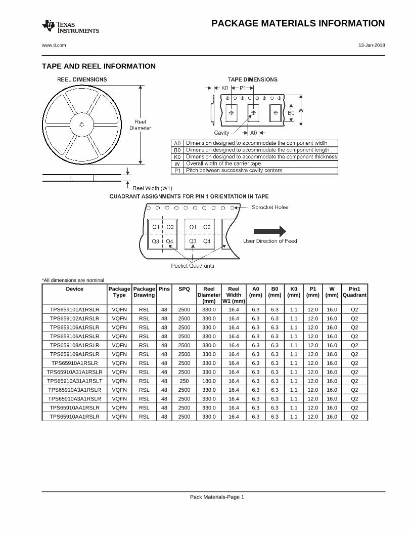
TAPE AND REEL INFORMATION
*All dimensions are nominal
Device PackageType
PackageDrawing
Pins SPQ ReelDiameter
(mm)
ReelWidth
W1 (mm)
A0(mm)
B0(mm)
K0(mm)
P1(mm)
W(mm)
Pin1Quadrant
TPS659101A1RSLR VQFN RSL 48 2500 330.0 16.4 6.3 6.3 1.1 12.0 16.0 Q2
TPS659102A1RSLR VQFN RSL 48 2500 330.0 16.4 6.3 6.3 1.1 12.0 16.0 Q2
TPS659106A1RSLR VQFN RSL 48 2500 330.0 16.4 6.3 6.3 1.1 12.0 16.0 Q2
TPS659106A1RSLR VQFN RSL 48 2500 330.0 16.4 6.3 6.3 1.1 12.0 16.0 Q2
TPS659108A1RSLR VQFN RSL 48 2500 330.0 16.4 6.3 6.3 1.1 12.0 16.0 Q2
TPS659109A1RSLR VQFN RSL 48 2500 330.0 16.4 6.3 6.3 1.1 12.0 16.0 Q2
TPS65910A1RSLR VQFN RSL 48 2500 330.0 16.4 6.3 6.3 1.1 12.0 16.0 Q2
TPS65910A31A1RSLR VQFN RSL 48 2500 330.0 16.4 6.3 6.3 1.1 12.0 16.0 Q2
TPS65910A31A1RSLT VQFN RSL 48 250 180.0 16.4 6.3 6.3 1.1 12.0 16.0 Q2
TPS65910A3A1RSLR VQFN RSL 48 2500 330.0 16.4 6.3 6.3 1.1 12.0 16.0 Q2
TPS65910A3A1RSLR VQFN RSL 48 2500 330.0 16.4 6.3 6.3 1.1 12.0 16.0 Q2
TPS65910AA1RSLR VQFN RSL 48 2500 330.0 16.4 6.3 6.3 1.1 12.0 16.0 Q2
TPS65910AA1RSLR VQFN RSL 48 2500 330.0 16.4 6.3 6.3 1.1 12.0 16.0 Q2
PACKAGE MATERIALS INFORMATION
www.ti.com 13-Jan-2018
Pack Materials-Page 1

*All dimensions are nominal
Device Package Type Package Drawing Pins SPQ Length (mm) Width (mm) Height (mm)
TPS659101A1RSLR VQFN RSL 48 2500 367.0 367.0 38.0
TPS659102A1RSLR VQFN RSL 48 2500 367.0 367.0 38.0
TPS659106A1RSLR VQFN RSL 48 2500 367.0 367.0 38.0
TPS659106A1RSLR VQFN RSL 48 2500 367.0 367.0 38.0
TPS659108A1RSLR VQFN RSL 48 2500 367.0 367.0 38.0
TPS659109A1RSLR VQFN RSL 48 2500 367.0 367.0 38.0
TPS65910A1RSLR VQFN RSL 48 2500 367.0 367.0 38.0
TPS65910A31A1RSLR VQFN RSL 48 2500 367.0 367.0 38.0
TPS65910A31A1RSLT VQFN RSL 48 250 210.0 185.0 35.0
TPS65910A3A1RSLR VQFN RSL 48 2500 367.0 367.0 38.0
TPS65910A3A1RSLR VQFN RSL 48 2500 367.0 367.0 38.0
TPS65910AA1RSLR VQFN RSL 48 2500 367.0 367.0 38.0
TPS65910AA1RSLR VQFN RSL 48 2500 367.0 367.0 38.0
PACKAGE MATERIALS INFORMATION
www.ti.com 13-Jan-2018
Pack Materials-Page 2

IMPORTANT NOTICE
Texas Instruments Incorporated (TI) reserves the right to make corrections, enhancements, improvements and other changes to itssemiconductor products and services per JESD46, latest issue, and to discontinue any product or service per JESD48, latest issue. Buyersshould obtain the latest relevant information before placing orders and should verify that such information is current and complete.TI’s published terms of sale for semiconductor products (http://www.ti.com/sc/docs/stdterms.htm) apply to the sale of packaged integratedcircuit products that TI has qualified and released to market. Additional terms may apply to the use or sale of other types of TI products andservices.Reproduction of significant portions of TI information in TI data sheets is permissible only if reproduction is without alteration and isaccompanied by all associated warranties, conditions, limitations, and notices. TI is not responsible or liable for such reproduceddocumentation. Information of third parties may be subject to additional restrictions. Resale of TI products or services with statementsdifferent from or beyond the parameters stated by TI for that product or service voids all express and any implied warranties for theassociated TI product or service and is an unfair and deceptive business practice. TI is not responsible or liable for any such statements.Buyers and others who are developing systems that incorporate TI products (collectively, “Designers”) understand and agree that Designersremain responsible for using their independent analysis, evaluation and judgment in designing their applications and that Designers havefull and exclusive responsibility to assure the safety of Designers' applications and compliance of their applications (and of all TI productsused in or for Designers’ applications) with all applicable regulations, laws and other applicable requirements. Designer represents that, withrespect to their applications, Designer has all the necessary expertise to create and implement safeguards that (1) anticipate dangerousconsequences of failures, (2) monitor failures and their consequences, and (3) lessen the likelihood of failures that might cause harm andtake appropriate actions. Designer agrees that prior to using or distributing any applications that include TI products, Designer willthoroughly test such applications and the functionality of such TI products as used in such applications.TI’s provision of technical, application or other design advice, quality characterization, reliability data or other services or information,including, but not limited to, reference designs and materials relating to evaluation modules, (collectively, “TI Resources”) are intended toassist designers who are developing applications that incorporate TI products; by downloading, accessing or using TI Resources in anyway, Designer (individually or, if Designer is acting on behalf of a company, Designer’s company) agrees to use any particular TI Resourcesolely for this purpose and subject to the terms of this Notice.TI’s provision of TI Resources does not expand or otherwise alter TI’s applicable published warranties or warranty disclaimers for TIproducts, and no additional obligations or liabilities arise from TI providing such TI Resources. TI reserves the right to make corrections,enhancements, improvements and other changes to its TI Resources. TI has not conducted any testing other than that specificallydescribed in the published documentation for a particular TI Resource.Designer is authorized to use, copy and modify any individual TI Resource only in connection with the development of applications thatinclude the TI product(s) identified in such TI Resource. NO OTHER LICENSE, EXPRESS OR IMPLIED, BY ESTOPPEL OR OTHERWISETO ANY OTHER TI INTELLECTUAL PROPERTY RIGHT, AND NO LICENSE TO ANY TECHNOLOGY OR INTELLECTUAL PROPERTYRIGHT OF TI OR ANY THIRD PARTY IS GRANTED HEREIN, including but not limited to any patent right, copyright, mask work right, orother intellectual property right relating to any combination, machine, or process in which TI products or services are used. Informationregarding or referencing third-party products or services does not constitute a license to use such products or services, or a warranty orendorsement thereof. Use of TI Resources may require a license from a third party under the patents or other intellectual property of thethird party, or a license from TI under the patents or other intellectual property of TI.TI RESOURCES ARE PROVIDED “AS IS” AND WITH ALL FAULTS. TI DISCLAIMS ALL OTHER WARRANTIES ORREPRESENTATIONS, EXPRESS OR IMPLIED, REGARDING RESOURCES OR USE THEREOF, INCLUDING BUT NOT LIMITED TOACCURACY OR COMPLETENESS, TITLE, ANY EPIDEMIC FAILURE WARRANTY AND ANY IMPLIED WARRANTIES OFMERCHANTABILITY, FITNESS FOR A PARTICULAR PURPOSE, AND NON-INFRINGEMENT OF ANY THIRD PARTY INTELLECTUALPROPERTY RIGHTS. TI SHALL NOT BE LIABLE FOR AND SHALL NOT DEFEND OR INDEMNIFY DESIGNER AGAINST ANY CLAIM,INCLUDING BUT NOT LIMITED TO ANY INFRINGEMENT CLAIM THAT RELATES TO OR IS BASED ON ANY COMBINATION OFPRODUCTS EVEN IF DESCRIBED IN TI RESOURCES OR OTHERWISE. IN NO EVENT SHALL TI BE LIABLE FOR ANY ACTUAL,DIRECT, SPECIAL, COLLATERAL, INDIRECT, PUNITIVE, INCIDENTAL, CONSEQUENTIAL OR EXEMPLARY DAMAGES INCONNECTION WITH OR ARISING OUT OF TI RESOURCES OR USE THEREOF, AND REGARDLESS OF WHETHER TI HAS BEENADVISED OF THE POSSIBILITY OF SUCH DAMAGES.Unless TI has explicitly designated an individual product as meeting the requirements of a particular industry standard (e.g., ISO/TS 16949and ISO 26262), TI is not responsible for any failure to meet such industry standard requirements.Where TI specifically promotes products as facilitating functional safety or as compliant with industry functional safety standards, suchproducts are intended to help enable customers to design and create their own applications that meet applicable functional safety standardsand requirements. Using products in an application does not by itself establish any safety features in the application. Designers mustensure compliance with safety-related requirements and standards applicable to their applications. Designer may not use any TI products inlife-critical medical equipment unless authorized officers of the parties have executed a special contract specifically governing such use.Life-critical medical equipment is medical equipment where failure of such equipment would cause serious bodily injury or death (e.g., lifesupport, pacemakers, defibrillators, heart pumps, neurostimulators, and implantables). Such equipment includes, without limitation, allmedical devices identified by the U.S. Food and Drug Administration as Class III devices and equivalent classifications outside the U.S.TI may expressly designate certain products as completing a particular qualification (e.g., Q100, Military Grade, or Enhanced Product).Designers agree that it has the necessary expertise to select the product with the appropriate qualification designation for their applicationsand that proper product selection is at Designers’ own risk. Designers are solely responsible for compliance with all legal and regulatoryrequirements in connection with such selection.Designer will fully indemnify TI and its representatives against any damages, costs, losses, and/or liabilities arising out of Designer’s non-compliance with the terms and provisions of this Notice.
Mailing Address: Texas Instruments, Post Office Box 655303, Dallas, Texas 75265Copyright © 2018, Texas Instruments Incorporated