CC115L Value Line Transmitter - TI.com · Product Folder Sample & Buy Technical Documents Tools &...
73
Product Folder Sample & Buy Technical Documents Tools & Software Support & Community CC115L SWRS105B – MAY 2011 – REVISED JUNE 2014 CC115L Value Line Transmitter 1 Device Overview 1.1 Features 1 • RF Performance • General – Programmable Output Power up to +12 dBm – Few External Components; Fully Integrated Frequency Synthesizer – Programmable Data Rate from 0.6 to 600 kbps – Green Package: RoHS Compliant and No – Frequency Bands: 300–348 MHz, Antimony or Bromine 387–464 MHz, and 779–928 MHz – Small Size (QLP 4- x 4-mm Package, 20 Pins) – 2-FSK, 4-FSK, GFSK, and OOK Supported – Suited for Systems Targeting Compliance with • Digital Features EN 300 220 V2.3.1 (Europe) and FCC CFR Part – Flexible Support for Packet Oriented Systems 15 (US) – On-chip Support for Sync Word Insertion, – Support for Asynchronous and Synchronous Flexible Packet Length, and Automatic CRC Serial Transmit Mode for Backward Calculation Compatibility with Existing Radio • Low-Power Features Communication Protocols – 200-nA Sleep Mode Current Consumption – Fast Startup Time; 240 μs From Sleep to TX Mode – 64-Byte TX FIFO 1.2 Applications • Ultra Low-Power Wireless Applications Operating • Remote Controls in the 315-, 433-, 868-, 915-MHz ISM or SRD • Toys Bands • Home and Building Automation • Wireless Alarm and Security Systems • Active RFID • Industrial Monitoring and Control 1.3 Description The CC115L is a cost optimized sub-1 GHz RF transmitter. The circuit is based on the popular CC1101 RF transceiver, and RF performance characteristics are identical. The CC115L value line transmitter together with the CC113L value line receiver enables a low-cost RF link. The RF transmitter is integrated with a highly configurable baseband modulator. The modem supports various modulation formats and has a configurable data rates from 0.6 to 600 kbps. The CC115L provides extensive hardware support for packet handling, data buffering, and burst transmissions. The main operating parameters and the 64-byte transmit FIFO of CC115L can be controlled through a serial peripheral interface (SPI). In a typical system, the CC115L will be used together with a microcontroller and a few additional passive components. Device Information (1) PART NUMBER PACKAGE BODY SIZE CC115LRGP QFN (20) 4.00 mm × 4.00 mm (1) For more information on these devices, see Section 8, Mechanical Packaging and Orderable Information. 1 An IMPORTANT NOTICE at the end of this data sheet addresses availability, warranty, changes, use in safety-critical applications, intellectual property matters and other important disclaimers. PRODUCTION DATA.
Transcript of CC115L Value Line Transmitter - TI.com · Product Folder Sample & Buy Technical Documents Tools &...

Product
Folder
Sample &Buy
Technical
Documents
Tools &
Software
Support &Community
CC115LSWRS105B –MAY 2011–REVISED JUNE 2014
CC115L Value Line Transmitter1 Device Overview
1.1 Features1
• RF Performance • General– Programmable Output Power up to +12 dBm – Few External Components; Fully Integrated
Frequency Synthesizer– Programmable Data Rate from 0.6 to 600 kbps– Green Package: RoHS Compliant and No– Frequency Bands: 300–348 MHz,
Antimony or Bromine387–464 MHz, and 779–928 MHz– Small Size (QLP 4- x 4-mm Package, 20 Pins)– 2-FSK, 4-FSK, GFSK, and OOK Supported– Suited for Systems Targeting Compliance with• Digital Features
EN 300 220 V2.3.1 (Europe) and FCC CFR Part– Flexible Support for Packet Oriented Systems15 (US)– On-chip Support for Sync Word Insertion,
– Support for Asynchronous and SynchronousFlexible Packet Length, and Automatic CRCSerial Transmit Mode for BackwardCalculationCompatibility with Existing Radio• Low-Power Features Communication Protocols
– 200-nA Sleep Mode Current Consumption– Fast Startup Time; 240 μs From Sleep to TX
Mode– 64-Byte TX FIFO
1.2 Applications• Ultra Low-Power Wireless Applications Operating • Remote Controls
in the 315-, 433-, 868-, 915-MHz ISM or SRD • ToysBands • Home and Building Automation
• Wireless Alarm and Security Systems • Active RFID• Industrial Monitoring and Control
1.3 DescriptionThe CC115L is a cost optimized sub-1 GHz RF transmitter. The circuit is based on the popular CC1101RF transceiver, and RF performance characteristics are identical. The CC115L value line transmittertogether with the CC113L value line receiver enables a low-cost RF link.
The RF transmitter is integrated with a highly configurable baseband modulator. The modem supportsvarious modulation formats and has a configurable data rates from 0.6 to 600 kbps.
The CC115L provides extensive hardware support for packet handling, data buffering, and bursttransmissions.
The main operating parameters and the 64-byte transmit FIFO of CC115L can be controlled through aserial peripheral interface (SPI). In a typical system, the CC115L will be used together with amicrocontroller and a few additional passive components.
Device Information (1)
PART NUMBER PACKAGE BODY SIZECC115LRGP QFN (20) 4.00 mm × 4.00 mm
(1) For more information on these devices, see Section 8, Mechanical Packaging and OrderableInformation.
1
An IMPORTANT NOTICE at the end of this data sheet addresses availability, warranty, changes, use in safety-critical applications,intellectual property matters and other important disclaimers. PRODUCTION DATA.

BIAS
PA
RBIAS XOSC_Q1
CSn
SI
SO (GDO1)
XOSC
SCLK
FREQ
SYNTH
Packet H
andle
r
Modula
tor
TX
FIF
O
Dig
italIn
terf
ace to M
CU
Radio Control
GDO0
RF_P
RF_N
GDO2
XOSC_Q2
CC115LSWRS105B –MAY 2011–REVISED JUNE 2014 www.ti.com
1.4 Functional Block DiagramFigure 1-1 shows a functional block diagram of the device.
Figure 1-1. Functional Block Diagram
2 Device Overview Copyright © 2011–2014, Texas Instruments IncorporatedSubmit Documentation Feedback
Product Folder Links: CC115L

CC115Lwww.ti.com SWRS105B –MAY 2011–REVISED JUNE 2014
Table of Contents1 Device Overview ......................................... 1 5.9 Modulation Formats ................................. 26
1.1 Features .............................................. 1 5.10 Radio Control........................................ 271.2 Applications........................................... 1 5.11 TX FIFO ............................................. 321.3 Description............................................ 1 5.12 Frequency Programming............................ 341.4 Functional Block Diagram ............................ 2 5.13 VCO ................................................. 35
2 Revision History ......................................... 4 5.14 Voltage Regulators.................................. 353 Terminal Configuration and Functions.............. 5 5.15 Output Power Programming ........................ 36
3.1 Pin Diagram .......................................... 5 5.16 General Purpose and Test Output Control Pins .... 383.2 Signal Descriptions ................................... 6 5.17 Asynchronous and Synchronous Serial Operation.. 40
4 Specifications ............................................ 7 5.18 System Considerations and Guidelines ............. 414.1 Absolute Maximum Ratings .......................... 7 5.19 Configuration Registers ............................. 434.2 Handling Ratings ..................................... 7 5.20 Development Kit Ordering Information.............. 574.3 Recommended Operating Conditions ................ 7 6 Applications, Implementation, and Layout........ 584.4 General Characteristics .............................. 7 6.1 Bias Resistor ........................................ 584.5 Current Consumption ................................. 8 6.2 Balun and RF Matching ............................. 584.6 RF Transmit Section.................................. 9 6.3 Crystal ............................................... 604.7 Crystal Oscillator .................................... 11 6.4 Reference Signal.................................... 604.8 Frequency Synthesizer Characteristics ............. 11 6.5 Additional Filtering .................................. 604.9 DC Characteristics .................................. 11 6.6 Power Supply Decoupling........................... 604.10 Power-On Reset .................................... 12 6.7 PCB Layout Recommendations..................... 614.11 Thermal Characteristics ............................. 12 7 Device and Documentation Support ............... 62
5 Detailed Description ................................... 13 7.1 Device Support ...................................... 625.1 Overview ............................................ 13 7.2 Documentation Support ............................. 635.2 Functional Block Diagram........................... 13 7.3 Trademarks.......................................... 635.3 Configuration Overview ............................. 14 7.4 Electrostatic Discharge Caution..................... 645.4 Configuration Software.............................. 16 7.5 Export Control Notice ............................... 645.5 4-wire Serial Configuration and Data Interface ..... 17 7.6 Glossary ............................................. 645.6 Microcontroller Interface and Pin Configuration..... 21 7.7 Additional Acronyms ................................ 645.7 Data Rate Programming ............................ 22 8 Mechanical Packaging and Orderable
Information .............................................. 665.8 Packet Handling Hardware Support................. 238.1 Packaging Information .............................. 66
Copyright © 2011–2014, Texas Instruments Incorporated Table of Contents 3Submit Documentation Feedback
Product Folder Links: CC115L

CC115LSWRS105B –MAY 2011–REVISED JUNE 2014 www.ti.com
2 Revision HistoryNOTE: Page numbers for previous revisions may differ from page numbers in the current version.
Changes from Revision A (September 2011) to Revision B Page
• Changed format of data sheet to standard TI format. ........................................................................... 1• Changed reset value from 0x09 to 0x19 ......................................................................................... 55• Changed the package designator from RTK to RGP .......................................................................... 66
4 Revision History Copyright © 2011–2014, Texas Instruments IncorporatedSubmit Documentation Feedback
Product Folder Links: CC115L

1
20 19 18 17 16
15
14
13
12
11
109876
5
4
3
2
GND
Exposed die
attach pad
SCLK
SO (GDO1)
GDO2
DVDD
DCOUPL
GD
O0
XO
SC
_Q
1
AVDDX
OS
C_
Q2
AV
DD
RF_P
RF_N
GN
D
AVDD
RB
IAS
DG
UA
RD
GN
D
SI
CS
n
AVDD
CC115Lwww.ti.com SWRS105B –MAY 2011–REVISED JUNE 2014
3 Terminal Configuration and Functions
3.1 Pin DiagramThe CC115L pinout is shown in Figure 3-1 and Table 3-1. See Section 5.16 for details on the I/Oconfiguration.
Figure 3-1. Pinout Top View
NOTEThe exposed die attach pad must be connected to a solid ground plane as this is the mainground connection for the chip.
Copyright © 2011–2014, Texas Instruments Incorporated Terminal Configuration and Functions 5Submit Documentation Feedback
Product Folder Links: CC115L

CC115LSWRS105B –MAY 2011–REVISED JUNE 2014 www.ti.com
3.2 Signal Descriptions
Table 3-1. Signal DescriptionsPin No. Pin Name Pin Type Description
1 SCLK Digital Serial configuration interface, clock inputInput
2 SO Digital Serial configuration interface, data output(GDO1) Output Optional general output pin when CSn is high
3 GDO2 Digital Digital output pin for general use:Output • Test signals
• TX FIFO status signals• Clock output, down-divided from XOSC
4 DVDD Power 1.8 - 3.6 V digital power supply for digital I/Os and for the digital core voltage regulator(Digital)
5 DCOUPL Power 1.6 - 2.0 V digital power supply output for decoupling(Digital)
NOTE: This pin is intended for use with the CC115L only. It can not be used to provide supplyvoltage to other devices
6 GDO0 Digital I/O Digital output pin for general use:• Test signals• TX FIFO status signals• Clock output, down-divided from XOSC• Serial input TX data
7 CSn Digital Serial configuration interface, chip selectInput
8 XOSC_Q1 Analog I/O Crystal oscillator pin 1, or external clock input9 AVDD Power 1.8 - 3.6 V analog power supply connection
(Analog)10 XOSC_Q2 Analog I/O Crystal oscillator pin 211 AVDD Power 1.8 - 3.6 V analog power supply connection
(Analog)12 RF_P RF I/O Positive RF output signal from PA in transmit mode13 RF_N RF I/O Negative RF output signal from PA in transmit mode14 AVDD Power 1.8 - 3.6 V analog power supply connection
(Analog)15 AVDD Power 1.8 - 3.6 V analog power supply connection
(Analog)16 GND Ground Analog ground connection
(Analog)17 RBIAS Analog I/O External bias resistor for reference current18 DGUARD Power Power supply connection for digital noise isolation
(Digital)19 GND Ground Ground connection for digital noise isolation
(Digital)20 SI Digital Serial configuration interface, data input
Input
6 Terminal Configuration and Functions Copyright © 2011–2014, Texas Instruments IncorporatedSubmit Documentation Feedback
Product Folder Links: CC115L

CC115Lwww.ti.com SWRS105B –MAY 2011–REVISED JUNE 2014
4 Specifications
4.1 Absolute Maximum RatingsUnder no circumstances must the absolute maximum ratings be violated. Stress exceeding one or more of the limiting valuesmay cause permanent damage to the device.Parameter Min Max Unit ConditionSupply voltage –0.3 3.9 V All supply pins must have the same voltage
VDD + 0.3,Voltage on any digital pin –0.3 Vmax 3.9Voltage on the pins RF_P, RF_N, –0.3 2.0 VDCOUPL, RBIASVoltage ramp-up rate 120 kV/µsInput RF level +10 dBm
4.2 Handling RatingsParameter MIN MAX UNITStorage temperature (default) –50 150 °Crange, Tstg
Human Body Model (HBM), per ANSI/ESDA/JEDEC JS001 (1) 750 VESD Stress Voltage,VESD Charged Device Model (CDM), per JJESD22-C101 (2) 400 V
(1) JEDEC document JEP155 states that 500-V HBM allows safe manufacturing with a standard ESD control process.(2) JEDEC document JEP157 states that 250-V HBM allows safe manufacturing with a standard ESD control process.
4.3 Recommended Operating ConditionsParameter Min Max Unit ConditionOperating temperature –40 85 °COperating supply voltage 1.8 3.6 V All supply pins must have the same voltage
4.4 General CharacteristicsParameter Min Typ Max Unit Condition
300 348 MHzIf using a 27 MHz crystal, the lower frequency limit for thisFrequency range 387 464 MHz band is 392 MHz
779 928 MHz0.6 500 kBaud 2-FSK0.6 250 kBaud GFSK and OOK
Data rate 0.6 300 kBaud 4-FSK (the data rate in kbps will be twice the baud rate)Optional Manchester encoding (the data rate in kbps will behalf the baud rate)
Copyright © 2011–2014, Texas Instruments Incorporated Specifications 7Submit Documentation Feedback
Product Folder Links: CC115L

CC115LSWRS105B –MAY 2011–REVISED JUNE 2014 www.ti.com
4.5 Current ConsumptionTA = 25°C, VDD = 3.0 V if nothing else stated. All measurement results are obtained using SWRR046 andSWRR045.
spacerParameter Min Typ Max Unit Condition
Voltage regulator to digital part off, register values retained0.2 1 µA (SLEEP state). All GDO pins programmed to 0x2F (HW to
0)Current consumption Voltage regulator to digital part off, register valuesin power down modes 100 µA retained, XOSC running (SLEEP state with
MCSM0.OSC_FORCE_ON set)Voltage regulator to digital part on, all other modules in165 µA power down (XOFF state)Only voltage regulator to digital part and crystal oscillator1.7 mA running (IDLE state)Only the frequency synthesizer is running (FSTXON state).Current consumptionThis current consumption is also representative for the8.4 mA other intermediate states when going from IDLE to TX,including the calibration state
27.4 mA Transmit mode, +10 dBm output powerCurrent consumption, 15.0 mA Transmit mode, 0 dBm output power315 MHz
12.3 mA Transmit mode, –6 dBm output power29.2 mA Transmit mode, +10 dBm output power
Current consumption, 16.0 mA Transmit mode, 0 dBm output power433 MHz13.1 mA Transmit mode, –6 dBm output power34.2 mA Transmit mode, +12 dBm output power, 868 MHz30.0 mA Transmit mode, +10 dBm output power, 868 MHz16.8 mA Transmit mode, 0 dBm output power, 868 MHz16.4 mA Transmit mode, –6 dBm output power, 868 MHz.Current consumption,
868/915 MHz 33.4 mA Transmit mode, +11 dBm output power, 915 MHz30.7 mA Transmit mode, +10 dBm output power, 915 MHz17.2 mA Transmit mode, 0 dBm output power, 915 MHz17.0 mA Transmit mode, –6 dBm output power, 915 MHz
4.5.1 Typical TX Current Consumption over Temperature and Supply Voltage, 868 MHzSupply Voltage Supply Voltage Supply Voltage
VDD = 1.8 V VDD = 3.0 V VDD = 3.6 VTemperature [°C] −40 25 85 −40 25 85 −40 25 85Current [mA], PATABLE=0xC0, +12 dBm 32.7 31.5 30.5 35.3 34.2 33.3 35.5 34.4 33.5Current [mA], PATABLE=0xC5, +10 dBm 30.1 29.2 28.3 30.9 30.0 29.4 31.1 30.3 29.6Current [mA], PATABLE=0x50, 0 dBm 16.4 16.0 15.6 17.3 16.8 16.4 17.6 17.1 16.7
4.5.2 Typical TX Current Consumption over Temperature and Supply Voltage, 915 MHzSupply Voltage Supply Voltage Supply Voltage
VDD = 1.8 V VDD = 3.0 V VDD = 3.6 VTemperature [°C] −40 25 85 −40 25 85 −40 25 85Current [mA], PATABLE=0xC0, +11 dBm 31.9 30.7 29.8 34.6 33.4 32.5 34.8 33.6 32.7Current [mA], PATABLE=0xC3, +10 dBm 30.9 29.8 28.9 31.7 30.7 30.0 31.9 31.0 30.2Current [mA], PATABLE=0x8E, 0 dBm 17.2 16.8 16.4 17.6 17.2 16.9 17.8 17.4 17.1
8 Specifications Copyright © 2011–2014, Texas Instruments IncorporatedSubmit Documentation Feedback
Product Folder Links: CC115L

CC115Lwww.ti.com SWRS105B –MAY 2011–REVISED JUNE 2014
4.6 RF Transmit SectionTA = 25°C, VDD = 3.0 V, +10 dBm if nothing else stated. All measurement results are obtained using SWRR046 andSWRR045.Parameter Min Typ Max Unit ConditionDifferential loadimpedance
Differential impedance as seen from the RF-port (RF_P315 MHz 122 + j31 Ωand RF_N) towards the antenna.
433 MHz 116 + j41 Ω868/915 MHz 86.5 + j43 ΩOutput power, highest Output power is programmable, and full range issetting available in all frequency bands. Output power may be
restricted by regulatory limits.315 MHz +10 dBm See Design Note DN013 SWRA168, which gives the433 MHz +10 dBm output power and harmonics when using multi-layer
inductors. The output power is then typically +10 dBm868 MHz +12 dBmwhen operating at 868/915 MHz.
915 MHz +11 dBm Delivered to a 50-Ω single-ended load through the RFmatching network in SWRR046 and SWRR045Output power is programmable, and full range is
Output power, lowest available in all frequency bands−30 dBmsetting Delivered to a 50-Ω single-ended load through the RFmatching network in SWRR046 and SWRR045
Harmonics, radiated Measured on SWRR046 and SWRR045 with CW,maximum output power2nd Harm, 433 MHz −49 dBm The antennas used during the radiated measurements
3rd Harm, 433 MHz −40 dBm (SMAFF-433 from R.W. Badland and Nearson S331868/915) play a part in attenuating the harmonics2nd Harm, 868 MHz −47 dBmNote: All harmonics are below −41.2 dBm when
3rd Harm, 868 MHz −55 dBm operating in the 902 - 928 MHz band2nd Harm, 915 MHz −50 dBm3rd Harm, 915 MHz −54 dBmHarmonics, conducted Measured with +10 dBm CW at 315 MHz and 433 MHz315 MHz < −35 dBm Frequencies below 960 MHz
< −53 dBm Frequencies above 960 MHz433 MHz −43 dBm Frequencies below 1 GHz
< −45 dBm Frequencies above 1 GHz868 MHz 2nd Harm −36 dBm Measured with +12 dBm CW at 868 MHzother harmonics < −46 dBm915 MHz 2nd Harm −34 dBm Measured with +11 dBm CW at 915 MHz (requirement isother harmonics −20 dBc under FCC 15.247)Other harmonics < −50 dBmSpurious emissions Measured with +10 dBm CW at 315 MHz and 433 MHzconducted, harmonicsnot included315 MHz < −58 Frequencies below 960 MHz
< −53 Frequencies above 960 MHz433 MHz < −50 Frequencies below 1 GHz
< −54 Frequencies above 1 GHz< −56 Frequencies within 47-74, 87.5-118, 174-230, 470-862
MHzMeasured with +12 dBm CW at 868 MHz
868 MHz < −50 Frequencies below 1 GHz< −52 Frequencies above 1 GHz< −53 Frequencies within 47-74, 87.5-118, 174-230, 470-862
MHz
Copyright © 2011–2014, Texas Instruments Incorporated Specifications 9Submit Documentation Feedback
Product Folder Links: CC115L

CC115LSWRS105B –MAY 2011–REVISED JUNE 2014 www.ti.com
TA = 25°C, VDD = 3.0 V, +10 dBm if nothing else stated. All measurement results are obtained using SWRR046 andSWRR045.Parameter Min Typ Max Unit Condition
All radiated spurious emissions are within the limits ofETSI. The peak conducted spurious emission is −53dBm at 699 MHz (868 MHz - 169 MHz), which is in afrequency band limited to −54 dBm by EN 300 220V2.3.1. An alternative filter can be used to reduce theemission at 699 MHz below −54 dBm, for conductedmeasurements, and is shown in Figure 6-2. See moreinformation in DN017 SWRA168.For compliance with modulation bandwidth requirementsunder EN 300 220 V2.3.1 in the 863 to 870 MHzfrequency range it is recommended to use a 26 MHzcrystal for frequencies below 869 MHz and a 27 MHzcrystal for frequencies above 869 MHz.Measured with +11 dBm CW at 915 MHz
< −51 Frequencies below 960 MHz915 MHz
< −54 Frequencies above 960 MHzTX latency 8 bit Serial operation. Time from sampling the data on the
transmitter data input pin until it is observed on the RFoutput ports.
4.6.1 Typical Variation in Output Power over Temperature and Supply Voltage, 868 MHzSupply Voltage Supply Voltage Supply Voltage
VDD = 1.8 V VDD = 3.0 V VDD = 3.6 VTemperature [°C] −40 25 85 −40 25 85 −40 25 85Output Power [dBm], PATABLE=0xC0, +12 dBm 12 11 10 12 12 11 12 12 11Output Power [dBm], PATABLE=0xC5, +10 dBm 11 10 9 11 10 10 11 10 10Output Power [dBm], PATABLE=0x50, 0 dBm 1 0 -1 2 1 0 2 1 0
4.6.2 Typical Variation in Output Power over Temperature and Supply Voltage, 915 MHzSupply Voltage Supply Voltage Supply Voltage
VDD = 1.8 V VDD = 3.0 V VDD = 3.6 VTemperature [°C] −40 25 85 −40 25 85 −40 25 85Output Power [dBm], PATABLE=0xC0, +11 dBm 11 10 10 12 11 11 12 11 11Output Power [dBm], PATABLE=0x8E, +0 dBm 2 1 0 2 1 0 2 1 0
10 Specifications Copyright © 2011–2014, Texas Instruments IncorporatedSubmit Documentation Feedback
Product Folder Links: CC115L

CC115Lwww.ti.com SWRS105B –MAY 2011–REVISED JUNE 2014
4.7 Crystal OscillatorTA = 25°C, VDD = 3.0 V if nothing else is stated. All measurement results obtained using SWRR046 and SWRR045.Parameter Min Typ Max Unit Condition
For compliance with modulation bandwidthrequirements under EN 300 220 V2.3.1 in the863 to 870 MHz frequency range it isCrystal frequency 26 26 27 MHz recommended to use a 26 MHz crystal forfrequencies below 869 MHz and a 27 MHzcrystal for frequencies above 869 MHz.This is the total tolerance including a) initialtolerance, b) crystal loading, c) aging, and d)
Tolerance ±40 ppm temperature dependence. The acceptablecrystal tolerance depends on RF frequencyand channel spacing / bandwidth.
Load capacitance 10 13 20 pF Simulated over operating conditionsESR 100 Ω
This parameter is to a large degree crystalStart-up time 150 µs dependent. Measured on SWRR046 and
SWRR045 using crystal AT-41CD2 from NDK
4.8 Frequency Synthesizer CharacteristicsTA = 25°C, VDD = 3.0 V if nothing else is stated. All measurement results are obtained using SWRR046 and SWRR045.Minimum figures are given using a 27 MHz crystal. Typical and maximum figures are given using a 26 MHz crystal.Parameter Min Typ Max Unit Condition
26- to 27-MHz crystal. The resolution (in Hz)Programmed frequency resolution 397 FXOSC/216 412 Hz is equal for all frequency bandsGiven by crystal used. Required accuracy(including temperature and aging) dependsSynthesizer frequency tolerance ±40 ppm on frequency band and channel bandwidth /spacing
RF carrier phase noise –92 dBc/Hz at 50 kHz offset from carrierRF carrier phase noise –92 dBc/Hz at 100 kHz offset from carrierRF carrier phase noise –92 dBc/Hz at 200 kHz offset from carrierRF carrier phase noise –98 dBc/Hz at 500 kHz offset from carrierRF carrier phase noise –107 dBc/Hz at 1 MHz offset from carrierRF carrier phase noise –113 dBc/Hz at 2 MHz offset from carrierRF carrier phase noise –119 dBc/Hz at 5 MHz offset from carrierRF carrier phase noise –129 dBc/Hz at 10 MHz offset from carrier
Time from leaving the IDLE state until arrivingPLL turn-on or hop time in the FSTXON or TX state, when not72 75 75 µs(See Table 5-5) performing calibration. Crystal oscillator
running.Calibration can be initiated manually orPLL calibration time 685 712 724 µs automatically before entering or after leaving(See Table 5-6) TX
4.9 DC CharacteristicsTA = 25°C if nothing else stated.Digital Inputs/Outputs Min Max Unit ConditionLogic "0" input voltage 0 0.7 VLogic "1" input voltage VDD – 0.7 VDD VLogic "0" output voltage 0 0.5 V For up to 4 mA output currentLogic "1" output voltage VDD – 0.3 VDD V For up to 4 mA output currentLogic "0" input current N/A –50 nA Input equals 0 VLogic "1" input current N/A 50 nA Input equals VDD
Copyright © 2011–2014, Texas Instruments Incorporated Specifications 11Submit Documentation Feedback
Product Folder Links: CC115L

CC115LSWRS105B –MAY 2011–REVISED JUNE 2014 www.ti.com
4.10 Power-On ResetFor proper Power-On-Reset functionality the power supply should comply with the requirements in Section 4.10. Otherwise,the chip should be assumed to have unknown state until transmitting an SRES strobe over the SPI interface. SeeSection 5.10.1, Power-On Start-Up Sequence, for further details.Parameter Min Typ Max Unit ConditionPower-up ramp-up time 5 ms From 0 V until reaching 1.8 V
Minimum time between power-on and power-Power off time 1 ms off
4.11 Thermal CharacteristicsNAME DESCRIPTION QFN (°C/W)RθJA Junction-to-ambient thermal resistance 47RθJC(top) Junction-to-case (top) thermal resistance 45RθJB Junction-to-board thermal resistance 13.6RθJC(bot) Junction-to-case (bottom) thermal resistance 5.12
12 Specifications Copyright © 2011–2014, Texas Instruments IncorporatedSubmit Documentation Feedback
Product Folder Links: CC115L

BIAS
PA
RBIAS XOSC_Q1
CSn
SI
SO (GDO1)
XOSC
SCLK
FREQ
SYNTH
Packet H
andle
r
Modula
tor
TX
FIF
O
Dig
italIn
terf
ace to M
CU
Radio Control
GDO0
RF_P
RF_N
GDO2
XOSC_Q2
CC115Lwww.ti.com SWRS105B –MAY 2011–REVISED JUNE 2014
5 Detailed Description
5.1 OverviewThe CC115L transmitter is based on direct synthesis of the RF frequency. The frequency synthesizerincludes a completely on-chip LC VCO.
A crystal is to be connected to XOSC_Q1 and XOSC_Q2. The crystal oscillator generates the referencefrequency for the synthesizer, as well as clocks for the ADC and the digital part.
A 4-wire SPI is used for configuration and data buffer access.
The digital baseband includes support for channel configuration, packet handling, and data buffering.
5.2 Functional Block DiagramA simplified block diagram of CC115L is shown in Figure 5-1.
Figure 5-1. CC115L Simplified Block Diagram
Copyright © 2011–2014, Texas Instruments Incorporated Detailed Description 13Submit Documentation Feedback
Product Folder Links: CC115L

CC115LSWRS105B –MAY 2011–REVISED JUNE 2014 www.ti.com
5.3 Configuration OverviewCC115L can be configured to achieve optimum performance for many different applications. Configurationis done using the SPI interface. See Section 5.5 for more description of the SPI interface. The followingkey parameters can be programmed:• Power-down / power up mode• Crystal oscillator power-up / power-down• Carrier frequency / RF channel• Transmit mode• Data rate• Modulation format• RF output power• Data buffering with separate 64-byte TX FIFO• Packet radio hardware support
Details of each configuration register can be found in Section 5.19.
Figure 5-2 shows a simplified state diagram that explains the main CC115L states together with typicalusage and current consumption. For detailed information on controlling the CC115L state machine, and acomplete state diagram, see Section 5.10.
14 Detailed Description Copyright © 2011–2014, Texas Instruments IncorporatedSubmit Documentation Feedback
Product Folder Links: CC115L

Transmit mode
IDLE
Manual freq.
synth. calibration
TX FIFO
underflow
Frequency
synthesizer on
SFSTXON
STX
STX
SFTX
SIDLE
SCAL
IDLE
TXOFF_MODE=00
STX or SFSTXON
Sleep
SPWD
Crystal
oscillator off
SXOFF
CSn=0
CSn=0
TXOFF_MODE=01
Frequency
synthesizer startup,
optional calibration,
settling
Optional freq.
synth. calibration
Default state when the radio is not
transmitting. Typ. current
consumption: 1.7 mA.
Lowest power mode. Most
register values are retained.
Typ. current consumption:
200 nA
All register values are
retained. Typ. current
consumption: 165 uA.
Used for calibrating frequency
synthesizer upfront (entering
transmit mode can then be
done quicker). Transitional
state. Typ. current
consumption: 8.4 mA.
Frequency synthesizer is turned on, can optionally be
calibrated, and then settles to the correct frequency.
Transitional state. Typ. current consumption: 8.4 mA.Frequency synthesizer is on,
ready to start transmitting.
Transmission starts very
quickly after receiving the STX
command strobe.Typ. current
consumption: 8.4 mA.
Typ. current consumption:
16.8 mA at 0 dBm output
power, 868 MHz
Optional transitional state.
Typ. current consumption: 8.4 mA.
In Normal mode, this state is
enetered if the TX FIFO is emptied
before the complete packet has
been written to the FIFO.
Typ. current consumption: 1.7 mA.
CC115Lwww.ti.com SWRS105B –MAY 2011–REVISED JUNE 2014
Figure 5-2. Simplified Radio Control State Diagram with Typical Current Consumption
Copyright © 2011–2014, Texas Instruments Incorporated Detailed Description 15Submit Documentation Feedback
Product Folder Links: CC115L

CC115LSWRS105B –MAY 2011–REVISED JUNE 2014 www.ti.com
5.4 Configuration SoftwareCC115L can be configured using the SmartRF™ Studio software SWRC176. The SmartRF Studiosoftware is highly recommended for obtaining optimum register settings, and for evaluating performanceand functionality.
After chip reset, all the registers have default values as shown Section 5.19. The optimum register settingmight differ from the default value. After a reset all registers that shall be different from the default valuetherefore needs to be programmed through the SPI interface.
16 Detailed Description Copyright © 2011–2014, Texas Instruments IncorporatedSubmit Documentation Feedback
Product Folder Links: CC115L

0 A5 A4 A3 A2 A0A1 DW7
1
Read from register:
Write to register:
Hi-Z
X
SCLK:
CSn:
SI
SO
SI
SO Hi-Z
tsp
tch
tcl
tsd
thd
tns
X X
Hi-Z
X
Hi-ZS7
X
DW6 DW5 DW4 DW3 DW2 DW1 DW0
B S5 S4 S3 S2 S1 S0 S7 S6 S5 S4 S3 S2 S1 S0
B
B A5 A4 A3 A2 A1 A0
S7 B S5 S4 S3 S2 S1 S0 DR7 DR6 DR5 DR4 DR3 DR2 DR1 DR0
CC115Lwww.ti.com SWRS105B –MAY 2011–REVISED JUNE 2014
5.5 4-wire Serial Configuration and Data InterfaceCC115L is configured through a simple 4-wire SPI-compatible interface (SI, SO, SCLK and CSn) whereCC115L is the slave. This interface is also used write buffered data. All transfers on the SPI interface aredone most significant bit first.
All transactions on the SPI interface start with a header byte containing a R/W bit, a burst access bit (B),and a 6-bit address (A5–A0).
The CSn pin must be kept low during transfers on the SPI bus. If CSn goes high during the transfer of aheader byte or during read/write from/to a register, the transfer will be cancelled. The timing for theaddress and data transfer on the SPI interface is shown in Figure 5-3 with reference to Table 5-1.
When CSn is pulled low, the MCU must wait until CC115L SO pin goes low before starting to transfer theheader byte. This indicates that the crystal is running. Unless the chip was in the SLEEP or XOFF states,the SO pin will always go low immediately after taking CSn low.
Figure 5-3. Configuration Registers Write and Read Operations
Table 5-1. SPI Interface Timing Requirements
Parameter Description Min Max UnitsSCLK frequency
– 10100 ns delay inserted between address byte and data byte (single access), orbetween address and data, and between each data byte (burst access).SCLK frequency, single accessfSCLK MHz– 9No delay between address and data byteSCLK frequency, burst access
– 6.5No delay between address and data byte, or between data bytes
tsp,pd CSn low to positive edge on SCLK, in power-down mode 150 – µstsp CSn low to positive edge on SCLK, in active mode 20 – nstch Clock high 50 – nstcl Clock low 50 – nstrise Clock rise time – 40 nstfall Clock fall time – 40 ns
Setup data (negative SCLK edge) to positive edge on Single access 55 –tsd SCLK (tsd applies between address and data bytes, ns
Burst access 76 –and between data bytes)thd Hold data after positive edge on SCLK 20 – nstns Negative edge on SCLK to CSn high. 20 – ns
Copyright © 2011–2014, Texas Instruments Incorporated Detailed Description 17Submit Documentation Feedback
Product Folder Links: CC115L

CC115LSWRS105B –MAY 2011–REVISED JUNE 2014 www.ti.com
NOTEThe minimum tsp,pd figure in Table 5-1 can be used in cases where the user does not readthe CHIP_RDYn signal. CSn low to positive edge on SCLK when the chip is woken frompower-down depends on the start-up time of the crystal being used. The 150 μs in Table 5-1is the crystal oscillator start-up time measured on SWRR046 and SWRR045 using crystalAT-41CD2 from NDK.
5.5.1 Chip Status ByteWhen the header byte, data byte, or command strobe is sent on the SPI interface, the chip status byte issent by the CC115L on the SO pin. The status byte contains key status signals, useful for the MCU. Thefirst bit, s7, is the CHIP_RDYn signal and this signal must go low before the first positive edge of SCLK.The CHIP_RDYn signal indicates that the crystal is running.
Bits 6, 5, and 4 comprise the STATE value. This value reflects the state of the chip. The XOSC and powerto the digital core are on in the IDLE state, but all other modules are in power down. The frequency andchannel configuration should only be updated when the chip is in this state.
The last four bits (3:0) in the status byte contains FIFO_BYTES_AVAILABLE. For these bits to give anyvalid information, the R/W bit in the header byte must be set to 0. The FIFO_BYTES_AVAILABLE fieldcontains the number of bytes that can be written to the TX FIFO. When FIFO_BYTES_AVAILABLE=15, 15or more bytes can be written.
Table 5-2 gives a status byte summary.
Table 5-2. Status Byte Summary
Bits Name DescriptionStays high until power and crystal have stabilized. Should always be low when7 CHIP_RDYn using the SPI interface.Indicates the current main state machine modeValue State Description
IDLE state000 IDLE (Also reported for some transitional states
instead of SETTLING or CALIBRATE)001 Reserved010 TX Transmit mode
6:4 STATE[2:0]011 FSTXON Fast TX ready
Frequency synthesizer calibration is100 CALIBRATE running101 SETTLING PLL is settling110 Reserved
TX FIFO has underflowed. Acknowledge111 TXFIFO_UNDERFLOW with SFTX3:0 FIFO_BYTES_AVAILABLE[3:0] The number of bytes that can be written to the TX FIFO
18 Detailed Description Copyright © 2011–2014, Texas Instruments IncorporatedSubmit Documentation Feedback
Product Folder Links: CC115L

SI HeaderSRES HeaderAddr Data
SO
CSn
CC115Lwww.ti.com SWRS105B –MAY 2011–REVISED JUNE 2014
5.5.2 Register AccessThe configuration registers on the CC115L are located on SPI addresses from 0x00 to 0x2E. Table 5-14lists all configuration registers. It is highly recommended to use SmartRF Studio SWRC176 to generateoptimum register settings. The detailed description of each register is found in Section 5.19.1 andSection 5.19.2. All configuration registers can be both written to and read. The R/W bit controls if theregister should be written to or read. When writing to registers, the status byte is sent on the SO pin eachtime a header byte or data byte is transmitted on the SI pin. When reading from registers, the status byteis sent on the SO pin each time a header byte is transmitted on the SI pin.
Registers with consecutive addresses can be accessed in an efficient way by setting the burst bit (B) inthe header byte. The address bits (A5 - A0) set the start address in an internal address counter. Thiscounter is incremented by one each new byte (every 8 clock pulses). The burst access is either a read ora write access and must be terminated by setting CSn high.
For register addresses in the range 0x30 - 0x3D, the burst bit is used to select between status registerswhen burst bit is one, and between command strobes when burst bit is zero (see Section 5.5.3). Becauseof this, burst access is not available for status registers and they must be accessed one at a time. Thestatus registers can only be read.
5.5.3 SPI ReadWhen reading register fields over the SPI interface while the register fields are updated by the radiohardware (that is, MARCSTATE or TXBYTES), there is a small, but finite, probability that a single readfrom the register is being corrupt. As an example, the probability of any single read from TXBYTES beingcorrupt, assuming the maximum data rate is used, is approximately 80 ppm. Refer to the CC115L ErrataNotes SWRZ037 for more details.
5.5.4 Command StrobesCommand Strobes may be viewed as single byte instructions to CC115L. By addressing a commandstrobe register, internal sequences will be started. These commands are used to disable the crystaloscillator, enable transmit mode, enable calibration etc. The 11 command strobes are listed in Table 5-13.
NOTEAn SIDLE strobe will clear all pending command strobes until IDLE state is reached. Thismeans that if for example an SIDLE strobe is issued while the radio is in TX state, any othercommand strobes issued before the radio reaches IDLE state will be ignored.
The command strobe registers are accessed by transferring a single header byte (no data is beingtransferred). That is, only the R/W bit, the burst access bit (set to 0), and the six address bits (in the range0x30 through 0x3D) are written. The R/W bit should be set to zero if the FIFO_BYTES_AVAILABLE fieldin the status byte should be interpreted.
When writing command strobes, the status byte is sent on the SO pin.
A command strobe may be followed by any other SPI access without pulling CSn high. However, if anSRES strobe is being issued, one will have to wait for SO to go low again before the next header byte canbe issued as shown in Figure 5-4. The command strobes are executed immediately, with the exception ofthe SPWD and the SXOFF strobes, which are executed when CSn goes high.
Figure 5-4. SRES Command Strobe
Copyright © 2011–2014, Texas Instruments Incorporated Detailed Description 19Submit Documentation Feedback
Product Folder Links: CC115L

Read or write consecutive
Write n + 1 bytes
registers (s):
to the TX FIFO:
HeaderStrobe HeaderStrobe HeaderStrobe
HeaderReg
HeaderReg n
HeaderFIFO
HeaderReg
Data
Datan
DataByte 0
Data
HeaderReg Data HeaderReg Data
Datan + 1 Datan + 2
HeaderStrobe HeaderReg Data HeaderStrobe HeaderFIFO
DataByte 1 DataByte 2 DataByte n - 1 DataByte n
DataByte 0 DataByte 1
CSn:
Command strobe(s):
Read or write register(s):
Combinations:
CC115LSWRS105B –MAY 2011–REVISED JUNE 2014 www.ti.com
5.5.5 TX FIFO AccessThe 64-byte TX FIFO is accessed through the 0x3F address. The TX FIFO is write-only and the R/W bitshould therefore be zero.
The burst bit is used to determine if the TX FIFO access is a single byte access or a burst access. Thesingle byte access method expects a header byte with the burst bit set to zero and one data byte. Afterthe data byte, a new header byte is expected; hence CSn can remain low. The burst access methodexpects one header byte and then consecutive data bytes until terminating the access by setting CSnhigh.
The following header bytes access the FIFO:• 0x3F: Single byte access to TX FIFO• 0x7F: Burst access to TX FIFO
When writing to the TX FIFO, the status byte (see Section 5.5.1) is output on SO for each new data byteas shown in Figure 5-3. This status byte can be used to detect TX FIFO underflow while writing data tothe TX FIFO. Note that the status byte contains the number of bytes free before writing the byte inprogress to the TX FIFO. When the last byte that fits in the TX FIFO is transmitted on SI, the status bytereceived concurrently on SO will indicate that one byte is free in the TX FIFO.
The TX FIFO may be flushed by issuing a SFTX command strobe. A SFTX command strobe can only beissued in the IDLE, or TXFIFO_UNDERFLOW states. The TX FIFO is flushed when going to the SLEEPstate.
Figure 5-5 gives a brief overview of different register access types possible.
5.5.6 PATABLE AccessThe 0x3E address is used to access the PATABLE, which is used for selecting PA power control settings.The SPI expects one or two data bytes after receiving the address (the burst bit must be set if two bytesare to be written). For OOK, two bytes should be written to PATABLE; the first byte after the address willset the logic 0 power level and the second byte written will set the logic 1 power level. For all othermodulations formats, only one byte should be written to PATABLE. Use SmartRF Studio SWRC176 orDN013 SWRA168 for recommended register values for a given output power.
The PATABLE can also be read by setting the R/W bit to 1. The read operation can be done as a singlebyte or burst access, depending on how many bytes should be read (one or two). Note that pulling CSnhigh will reset the index counter to zero, meaning that burst access needs to be used for reading/writingthe second PATABLE entry. For the same reason, if one byte is written to the PATABLE and this value isto be read out, CSn must be set high before the read access in order to set the index counter back tozero.
The content of the PATABLE is lost when entering the SLEEP state, except for the first byte, meaning thatif OOK is used, the PATABLE needs to be reprogrammed when waking up from SLEEP.
Figure 5-5. Register Access Types
20 Detailed Description Copyright © 2011–2014, Texas Instruments IncorporatedSubmit Documentation Feedback
Product Folder Links: CC115L

CC115Lwww.ti.com SWRS105B –MAY 2011–REVISED JUNE 2014
5.6 Microcontroller Interface and Pin ConfigurationIn a typical system, CC115L will interface to a microcontroller. This microcontroller must be able to:• Program CC115L into different modes• Write buffered data• Read back status information through the 4-wire SPI-bus configuration interface (SI, SO, SCLK, and
CSn)
5.6.1 Configuration InterfaceThe microcontroller uses four I/O pins for the SPI configuration interface (SI, SO, SCLK, and CSn). TheSPI is described in Section 5.5.
5.6.2 General Control and Status PinsThe CC115L has two dedicated configurable pins (GDO0 and GDO2) and one shared pin (GDO1) thatcan output internal status information useful for control software. These pins can be used to generateinterrupts on the MCU. See Section 5.16 for more details on the signals that can be programmed.
GDO1 is shared with the SO pin in the SPI interface. The default setting for GDO1/SO is 3-state output.By selecting any other of the programming options, the GDO1/SO pin will become a generic pin. WhenCSn is low, the pin will always function as a normal SO pin.
In the synchronous and asynchronous serial modes, the GDO0 pin is used as a serial TX data input pinwhile in transmit mode.
Copyright © 2011–2014, Texas Instruments Incorporated Detailed Description 21Submit Documentation Feedback
Product Folder Links: CC115L

28DATA
DRATE _EXOSC
R 2DRATE _M 256
ƒ 2
×
= -
×
20DATA
2XOSC
R 2DRATE _E log
ƒ
æ ö×= ç ÷
ç ÷è ø
DRATE _E
DATA XOSC28
(256 DRATE _M) 2R ƒ
2
+ ×= ×
CC115LSWRS105B –MAY 2011–REVISED JUNE 2014 www.ti.com
5.7 Data Rate ProgrammingThe data rate used when transmitting is programmed by the MDMCFG3.DRATE_M and theMDMCFG4.DRATE_E configuration registers. The data rate is given by the formula below. As the formulashows, the programmed data rate depends on the crystal frequency.
(1)
The following approach can be used to find suitable values for a given data rate:
(2)
(3)
If DRATE_M is rounded to the nearest integer and becomes 256, increment DRATE_E and useDRATE_M = 0.
The data rate can be set from 0.6 kBaud to 500 kBaud with the minimum step size according to Table 5-3.See Section 4.4 for the minimum and maximum data rates for the different modulation formats.
Table 5-3. Data Rate Step Size (Assuming a 26-MHz Crystal)
Min Data Rate [kBaud] Typical Data Rate [kBaud] Max Data Rate [kBaud] Data rate Step Size [kBaud]0.6 1.0 0.79 0.00150.79 1.2 1.58 0.00311.59 2.4 3.17 0.00623.17 4.8 6.33 0.01246.35 9.6 12.7 0.024812.7 19.6 25.3 0.049625.4 38.4 50.7 0.099250.8 76.8 101.4 0.1984
101.6 153.6 202.8 0.3967203.1 250 405.5 0.7935406.3 500 500 1.5869
22 Detailed Description Copyright © 2011–2014, Texas Instruments IncorporatedSubmit Documentation Feedback
Product Folder Links: CC115L

Preamble bits
(1010...1010)
Syn
cW
ord
Len
gth
Fie
ld
Ad
dre
ss F
ield
Data Field
CR
C-1
6
Optional CRC-16 Calculation
8 x nbits 16 /32 bits8
bits
8
bits8 x n bits 16 bits
Legend:
Inserted automatically
Optional user-provided fields (the length field is
processed by the radio)
Unprocessed user data
CC115Lwww.ti.com SWRS105B –MAY 2011–REVISED JUNE 2014
5.8 Packet Handling Hardware SupportThe CC115L has built-in hardware support for packet oriented radio protocols. The packet handler can beconfigured to add the following elements to the packet stored in the TX FIFO:• A programmable number of preamble bytes• A two byte synchronization (sync) word. Can be duplicated to give a 4-byte sync word. It is not
possible to only insert preamble or only insert a sync word• A CRC checksum computed over the data field.• In a system where the CC115L is transmitting packets to the CC110L, CC113L or CC1101, the
recommended setting is 4- byte preamble and 4-byte sync word, except for 500 kBaud data rate wherethe recommended preamble length is 8 bytes.
NOTERegister fields that control the packet handling features should only be altered when CC115Lis in the IDLE state.
5.8.1 Packet FormatThe format of the data packet can be configured and consists of the following items (see Figure 5-6):• Preamble• Synchronization word• Optional length byte• Optional address byte• Payload• Optional 2 byte CRC
Figure 5-6. Packet Format
The preamble pattern is an alternating sequence of ones and zeros (10101010…). The minimum length ofthe preamble is programmable through the value of MDMCFG1.NUM_PREAMBLE. When enabling TX,the modulator will start transmitting the preamble. When the programmed number of preamble bytes hasbeen transmitted, the modulator will send the sync word and then data from the TX FIFO if data isavailable. If the TX FIFO is empty, the modulator will continue to send preamble bytes until the first byte iswritten to the TX FIFO. The modulator will then send the sync word and then the data bytes.
The synchronization word is a two-byte value set in the SYNC1 and SYNC0 registers. If the CC110L,CC113L, or CC1101 are used at the receiving end, they will need the sync word for byte synchronizationof the incoming packet. The synchronization word is automatically inserted by the CC115L. A one-bytesync word can be emulated by setting the SYNC1 value to the preamble pattern. It is also possible toemulate a 32 bit sync word by setting MDMCFG2.SYNC_MODE to 3. The sync word will then be repeatedtwice.
CC115L supports both constant packet length protocols and variable length protocols. Variable or fixedpacket length mode can be used for packets up to 255 bytes. For longer packets, infinite packet lengthmode must be used.
Copyright © 2011–2014, Texas Instruments Incorporated Detailed Description 23Submit Documentation Feedback
Product Folder Links: CC115L

Internal byte counter in packet handler counts from 0 to 255 and then starts at 0 again
0, 1............, 88, .............................................255, 0, ........, 88, .............................................255, 0, ........, 88, .............................................255, 0, ..
Infinite packet length mode enabled Fixed packet length mode anbled when
less than 256 bytes remains of packet
600 bytes transmitted
Length field transmitted. PKTLEN set to
mod(600, 256) = 88
CC115LSWRS105B –MAY 2011–REVISED JUNE 2014 www.ti.com
Fixed packet length mode is selected by setting PKTCTRL0.LENGTH_CONFIG=0. The desired packetlength is set by the PKTLEN register. This value must be different from 0.
In variable packet length mode, PKTCTRL0.LENGTH_CONFIG=1, the packet length is configured by thefirst byte transmitted after the sync word. The packet length is defined as the payload data, excluding thelength byte and the optional CRC. The PKTLEN value must be different from 0.
With PKTCTRL0.LENGTH_CONFIG=2, the packet length is set to infinite and transmission will continueuntil turned off manually. As described in , this can be used to support packet formats with different lengthconfiguration than natively supported by CC115L. One should make sure that TX mode is not turned offduring the transmission of the first half of any byte. Refer to the CC115L Errata Notes SWRZ036 for moredetails.
NOTEThe minimum packet length supported (excluding the optional length byte and CRC) is onebyte of payload data.
5.8.1.1 Packet Length > 255
The packet automation control register, PKTCTRL0, can be reprogrammed during TX. This opens thepossibility to transmit packets that are longer than 256 bytes and still be able to use the packet handlinghardware support. At the start of the packet, the infinite packet length mode (PKTCTRL0.LENGTH_CONFIG=2) must be active and the PKTLEN register is set to mod(length, 256).When less than 256 bytes remains of the packet, the MCU disables infinite packet length mode andactivates fixed packet length mode ( PKTCTRL0.LENGTH_CONFIG=0). When the internal byte counterreaches the PKTLEN value, the transmission ends (the radio enters the state determined byTXOFF_MODE). Automatic CRC appending/checking can also be used (by settingPKTCTRL0.CRC_EN=1).
When for example a 600-byte packet is to be transmitted, the MCU should do the following (see Figure 5-7).• Set PKTCTRL0.LENGTH_CONFIG=2.• Pre-program the PKTLEN register to mod(600, 256) = 88.• Transmit at least 345 bytes (600 - 255), for example by filling the 64-byte TX FIFO six times (384 bytes
transmitted).• Set PKTCTRL0.LENGTH_CONFIG=0.• The transmission ends when the packet counter reaches 88. A total of 600 bytes are transmitted.
Figure 5-7. Packet Length > 255
24 Detailed Description Copyright © 2011–2014, Texas Instruments IncorporatedSubmit Documentation Feedback
Product Folder Links: CC115L

CC115Lwww.ti.com SWRS105B –MAY 2011–REVISED JUNE 2014
5.8.2 Packet HandlingThe payload that is to be transmitted must be written into the TX FIFO. The first byte written must be thelength byte when variable packet length is enabled. The length byte has a value equal to the payload ofthe packet (including the optional address byte). If the receiver is the CC110L, CC113L, or CC1101, andaddress recognition is enabled, the second byte written to the TX FIFO must be the address byte.
If fixed packet length is enabled, the first byte written to the TX FIFO should be the address (assuming thereceiver uses address recognition).
The modulator will first send the programmed number of preamble bytes. If data is available in the TXFIFO, the modulator will send the two-byte (optionally 4-byte) sync word followed by the payload in the TXFIFO. If CRC is enabled, the checksum is calculated over all the data pulled from the TX FIFO, and theresult is sent as two extra bytes following the payload data. If the TX FIFO runs empty before thecomplete packet has been transmitted, the radio will enter TXFIFO_UNDERFLOW state. The only way toexit this state is by issuing an SFTX strobe. Writing to the TX FIFO after it has underflowed will not restartTX mode.
5.8.3 Packet Handling in FirmwareWhen implementing a packet oriented radio protocol in firmware, the MCU needs to know when a packethas been transmitted. Additionally, for packets longer than 64 bytes, the TX FIFO needs to be refilledwhile in TX. This means that the MCU needs to know the number of bytes that can be written to the TXFIFO. There are two possible solutions to get the necessary status information:
a. Interrupt Driven Solution
The GDO pins can be used to give an interrupt when a sync word has been transmitted or when acomplete packet has been transmitted by setting IOCFGx.GDOx_CFG=0x06. In addition, there are twoconfigurations for the IOCFGx.GDOx_CFG register that can be used as an interrupt source to provideinformation on how many bytes that are in the TX FIFO (IOCFGx.GDOx_CFG=0x02 andIOCFGx.GDOx_CFG=0x03). See Table 5-12 for more information.
b. SPI Polling
The PKTSTATUS register can be polled at a given rate to get information about the current GDO2 andGDO0 values respectively. The TXBYTES registers can be polled at a given rate to get information aboutthe number of bytes in the and TX FIFO. Alternatively, the number of bytes in the TX FIFO can be readfrom the chip status byte returned on the MISO line each time a header byte, data byte, or commandstrobe is sent on the SPI bus.
It is recommended to employ an interrupt driven solution due to a small, but finite, probability that a singleread from registers PKTSTATUS and TXBYTES is being corrupt. The same is the case when reading thechip status byte (see Section 5.5.3 and the CC115L Errata Notes SWRZ036).
Copyright © 2011–2014, Texas Instruments Incorporated Detailed Description 25Submit Documentation Feedback
Product Folder Links: CC115L

+1
+1/3
-1/3
-11 0 1 0 1 0 1 0 1 1 0 1 0 0 1 1 00 01 01 11 10 00 11 01
Preamble
0xAA
Sync
0xD3
Data
0x17 0x8D
1/Baud Rate 1/Baud Rate 1/Baud Rate
DEVIATION_EXOSCdev 17
ƒƒ (8 DEVIATION_M) 2
2= × + ×
CC115LSWRS105B –MAY 2011–REVISED JUNE 2014 www.ti.com
5.9 Modulation FormatsCC115L supports amplitude, frequency, and phase shift modulation formats. The desired modulationformat is set in the MDMCFG2.MOD_FORMAT register.
Optionally, the data stream can be Manchester coded by the modulator by settingMDMCFG2.MANCHESTER_EN=1.
NOTEManchester encoding is not supported at the same time as using 4-FSK modulation.
5.9.1 Frequency Shift KeyingCC115L supports 2-(G)FSK and 4-FSK modulation. When selecting 4-FSK, the preamble and sync wordis sent using 2-FSK (see Figure 5-8).
The frequency deviation is programmed with the DEVIATION_M and DEVIATION_E values in theDEVIATN register. The value has an exponent/mantissa form, and the resultant deviation is given by:
(4)
The symbol encoding is shown in Table 5-4.
Table 5-4. Symbol Encoding for 2-FSK/GFSK and 4-FSK Modulation
Format Symbol Coding0 – Deviation
2-FSK/GFSK1 + Deviation01 – Deviation00 – 1/3×Deviation
4-FSK10 + 1/3×Deviation11 + Deviation
Figure 5-8. Data Sent Over the Air ( MDMCFG2.MOD_FORMAT=100)
5.9.2 Amplitude ModulationThe amplitude modulation supported by CC115L is On-Off Keying (OOK). OOK modulation simply turnsthe PA on or off to modulate ones and zeros respectively.
The DEVIATN register setting has no effect when using OOK.
26 Detailed Description Copyright © 2011–2014, Texas Instruments IncorporatedSubmit Documentation Feedback
Product Folder Links: CC115L

TX
19,20
IDLE
1
CALIBRATE
8
MANCAL
3,4,5
SETTLING
9,10
TX_UNDERFLOW
22
FSTXON
18
SFSTXON
FS_AUTOCAL = 00 | 10 | 11
and
STX | SFSTXON
STX
STX
TXFIFO_UNDERFLOW
SFTX
SIDLE
SCAL
CAL_COMPLETE
FS_AUTOCAL = 01
and
STX | SFSTXON
CAL_COMPLETE
CALIBRATE
12
IDLE
1
TXOFF_MODE = 00
and
FS_AUTOCAL = 10 | 11
TXOFF_MODE = 00
and
FS_AUTOCAL = 00 | 01
TXOFF_MODE = 10
FS_WAKEUP
6,7
STX | SFSTXON
SLEEP
0SPWD
XOFF
2
SXOFF
CSn = 0
CSn = 0
TXOFF_MODE = 01
CC115Lwww.ti.com SWRS105B –MAY 2011–REVISED JUNE 2014
5.10 Radio Control
Figure 5-9. Complete Radio Control State Diagram
CC115L has a built-in state machine that is used to switch between different operational states (modes).The change of state is done either by using command strobes or by internal events such as TX FIFOunderflow.
A simplified state diagram, together with typical usage and current consumption, is shown in Figure 5-2.The complete radio control state diagram is shown in Figure 5-9. The numbers refer to the state numberreadable in the MARCSTATE status register. This register is primarily for test purposes.
Copyright © 2011–2014, Texas Instruments Incorporated Detailed Description 27Submit Documentation Feedback
Product Folder Links: CC115L

CSn
SO
XOSC Stable
XOSC and voltage regulator switched on
SI SRES
40 us
XOSC Stable
CSn
SO
CC115LSWRS105B –MAY 2011–REVISED JUNE 2014 www.ti.com
5.10.1 Power-On Start-Up SequenceWhen the power supply is turned on, the system must be reset. This is achieved by one of the twosequences described below, that is, automatic power-on reset (POR) or manual reset. After the automaticpower-on reset or manual reset, it is also recommended to change the signal that is output on the GDO0pin. The default setting is to output a clock signal with a frequency of CLK_XOSC/192. However, tooptimize performance in TX, an alternative GDO setting from the settings found in Table 5-12 should beselected.
5.10.1.1 Automatic POR
A power-on reset circuit is included in the CC115L. The minimum requirements stated in Section 4.10must be followed for the power-on reset to function properly. The internal power-up sequence iscompleted when CHIP_RDYn goes low. CHIP_RDYn is observed on the SO pin after CSn is pulled low.See Section 5.5.1 for more details on CHIP_RDYn.
When the CC115L reset is completed, the chip will be in the IDLE state and the crystal oscillator will berunning. If the chip has had sufficient time for the crystal oscillator to stabilize after the power-on-reset, theSO pin will go low immediately after taking CSn low. If CSn is taken low before reset is completed, the SOpin will first go high, indicating that the crystal oscillator is not stabilized, before going low as shown inFigure 5-10.
Figure 5-10. Power-On Reset with SRES
5.10.1.2 Manual Reset
The other global reset possibility on CC115L uses the SRES command strobe. By issuing this strobe, allinternal registers and states are set to the default, IDLE state. The manual power-up sequence is asfollows (see Figure 5-11):• Set SCLK = 1 and SI = 0.• Strobe CSn low / high.• Hold CSn low and then high for at least 40 µs relative to pulling CSn low• Pull CSn low and wait for SO to go low ( CHIP_RDYn).• Issue the SRES strobe on the SI line.• When SO goes low again, reset is complete and the chip is in the IDLE state.
XOSC and voltage regulator switched on
Figure 5-11. Power-On Reset with SRES
28 Detailed Description Copyright © 2011–2014, Texas Instruments IncorporatedSubmit Documentation Feedback
Product Folder Links: CC115L

CC115Lwww.ti.com SWRS105B –MAY 2011–REVISED JUNE 2014
NOTEThe above reset procedure is only required just after the power supply is first turned on. Ifthe user wants to reset the CC115L after this, it is only necessary to issue an SREScommand strobe.
5.10.2 Crystal ControlThe crystal oscillator (XOSC) is either automatically controlled or always on, ifMCSM0.XOSC_FORCE_ON is set.
In the automatic mode, the XOSC will be turned off if the SXOFF or SPWD command strobes are issued;the state machine then goes to XOFF or SLEEP respectively. This can only be done from the IDLE state.The XOSC will be turned off when CSn is released (goes high). The XOSC will be automatically turned onagain when CSn goes low. The state machine will then go to the IDLE state. The SO pin on the SPIinterface must be pulled low before the SPI interface is ready to be used as described in Section 5.5.1.
If the XOSC is forced on, the crystal will always stay on even in the SLEEP state.
Crystal oscillator start-up time depends on crystal ESR and load capacitances. The electrical specificationfor the crystal oscillator can be found in Section 4.7.
5.10.3 Voltage Regulator ControlThe voltage regulator to the digital core is controlled by the radio controller. When the chip enters theSLEEP state which is the state with the lowest current consumption, the voltage regulator is disabled. Thisoccurs after CSn is released when a SPWD command strobe has been sent on the SPI interface. Thechip is then in the SLEEP state. Setting CSn low again will turn on the regulator and crystal oscillator andmake the chip enter the IDLE state.
Copyright © 2011–2014, Texas Instruments Incorporated Detailed Description 29Submit Documentation Feedback
Product Folder Links: CC115L

CC115LSWRS105B –MAY 2011–REVISED JUNE 2014 www.ti.com
5.10.4 Transmit Mode (TX)Transmit mode is activated directly by the MCU by using the STX command strobe.
The frequency synthesizer must be calibrated regularly. CC115L has one manual calibration option (usingthe SCAL strobe), and three automatic calibration options that are controlled by theMCSM0.FS_AUTOCAL setting:• Calibrate when going from IDLE to TX (or FSTXON)• Calibrate when going from TX to IDLE automatically (not forced in IDLE by issuing an SIDLE strobe)• Calibrate every fourth time when going from TX to IDLE automatically (not forced in IDLE by issuing an
SIDLE strobe)
If the radio goes from TX to IDLE by issuing an SIDLE strobe, calibration will not be performed. Thecalibration takes a constant number of XOSC cycles; see Table 5-5 for timing details regarding calibration.
When TX is active the chip will remain in the TX state until the current packet has been successfullytransmitted. Then the state will change as indicated by the MCSM1.TXOFF_MODE setting. The possibledestinations are:• IDLE• FSTXON: Frequency synthesizer on and ready at the TX frequency. Activate TX with STX• TX: Start sending preamble
The SIDLE command strobe can always be used to force the radio controller to go to the IDLE state.
5.10.5 Timing
5.10.5.1 Overall State Transition Times
The main radio controller needs to wait in certain states in order to make sure that the internalanalog/digital parts have settled down and are ready to operate in the new states. A number of factors areimportant for the state transition times:• The crystal oscillator frequency, fxosc
• OOK used or not• The data rate in cases where OOK is used• The value of the TEST0, TEST1, and FSCAL3 registers
Table 5-5 shows timing in crystal clock cycles for key state transitions.
Note that the TX to IDLE transition time is a function of data rate (fbaudrate). When OOK is used (that is,FREND0.PA_POWER=001b), TX to IDLE will require 1/8×f baudrate longer times than the time stated inTable 5-5.
30 Detailed Description Copyright © 2011–2014, Texas Instruments IncorporatedSubmit Documentation Feedback
Product Folder Links: CC115L

CC115Lwww.ti.com SWRS105B –MAY 2011–REVISED JUNE 2014
Table 5-5. Overall State Transition Times [Example for 26-MHz Crystal Oscillator, 250 kBaud Data Rate,and TEST0 = 0x0B (Maximum Calibration Time)].
Description Transition Time (FREND0.PA_POWER=0) Transition Time [µs]IDLE to TX/FSTXON, no calibration 1954/fxosc 75.2
IDLE to TX/FSTXON, with calibration 1953/fxosc + FS calibration Time 799TX to IDLE, no calibration ~0.25/fbaudrate ~1
TX to IDLE, with calibration ~0.25/fbaudrate + FS calibration Time 725Manual calibration 283/fxosc + FS calibration Time 735
5.10.5.2 Frequency Synthesizer Calibration Time
Table 5-6 summarizes the frequency synthesizer (FS) calibration times for possible settings of TEST0 andFSCAL3.CHP_CURR_CAL_EN. Setting FSCAL3.CHP_CURR_CAL_EN to 00b disables the charge pumpcalibration stage. TEST0 is set to the values recommended by SmartRF Studio software SWRC176. Thepossible values for TEST0 when operating with different frequency bands are 0x09 and 0x0B. SmartRFStudio software always sets FSCAL3.CHP_CURR_CAL_EN to 10b.
The calibration time can be reduced from 712/724 µs to 145/157 µs. See Section 5.18.2 for more details.
Table 5-6. Frequency Synthesizer Calibration Times (26- and 27-MHz Crystal)
TEST0 FSCAL3.CHP_CURR_CAL_EN FS Calibration Time fxosc = 26 FS Calibration Time fxosc = 27MHz MHz
0x09 00b 3764/fxosc = 145 µs 3764/fxosc = 139 µs0x09 10b 18506/fxosc = 712 µs 18506/fxosc = 685 µs0x0B 00b 4073/fxosc = 157 µs 4073/fxosc = 151 µs0x0B 10b 18815/fxosc = 724 µs 18815/fxosc = 697 µs
Copyright © 2011–2014, Texas Instruments Incorporated Detailed Description 31Submit Documentation Feedback
Product Folder Links: CC115L

CC115LSWRS105B –MAY 2011–REVISED JUNE 2014 www.ti.com
5.11 TX FIFOThe CC115L contains a 64-byte TX FIFO for data to be transmitted and the SPI interface is used to writeto the TX FIFO (see Section 5.5.5 for more details). The FIFO controller will detect underflow in the TXFIFO.
When writing to the TX FIFO it is the responsibility of the MCU to avoid TX FIFO overflow. A TX FIFOoverflow will result in an error in the TX FIFO content.
The chip status byte that is available on the SO pin while transferring the SPI header and contains the fillgrade of the TX FIFO if the access is a write operation. Section 5.5.1 contains more details on this.
The number of bytes in the TX FIFO can be read from the status registers TXBYTES.NUM_TXBYTES.
The 4-bit FIFOTHR.FIFO_THR setting is used to program threshold points in the TX FIFO.
Table 5-7 lists the 16 FIFO_THR settings and the corresponding thresholds for the TX FIFO.
Table 5-7. FIFO_THR Settings and the Corresponding FIFO Thresholds
FIFO_THR Bytes in TX FIFO0 (0000) 611 (0001) 572 (0010) 533 (0011) 494 (0100) 455 (0101) 416 (0110) 377 (0111) 338 (1000) 299 (1001) 25
10 (1010) 2111 (1011) 1712 (1100) 1313 (1101) 914 (1110) 515 (1111) 1
A signal will assert when the number of bytes in the TX FIFO is equal to or higher than the programmedthreshold. This signal can be viewed on the GDO pins (see Table 5-12).
Figure 5-12 shows the number of bytes in the TX FIFO when the threshold signal toggles in the case ofFIFO_THR=13. Figure 5-13 shows the signal on the GDO pin as the TX FIFO is filled above the threshold,and then drained below in the case of FIFO_THR=13.
32 Detailed Description Copyright © 2011–2014, Texas Instruments IncorporatedSubmit Documentation Feedback
Product Folder Links: CC115L

6 7 8 9 678910NUM_TXBYTES
GDO
8 bytesUnderflow
margin
TX FIFO
FIFO_THR=13
CC115Lwww.ti.com SWRS105B –MAY 2011–REVISED JUNE 2014
Figure 5-12. Example of FIFO at Threshold
Figure 5-13. Number of Bytes in TX FIFO vs. the GDO Signal (GDOx_CFG=0x02 and FIFO_THR=13)
Copyright © 2011–2014, Texas Instruments Incorporated Detailed Description 33Submit Documentation Feedback
Product Folder Links: CC115L

XOSCIF 10
ƒƒ FREQ _IF
2= ×
CHANSPC_ 2 2XOSCcarrier 16
ƒƒ (FREQ CHAN ((256 CHANSPC _M) 2 ))
2
-= × + × + ×
CC115LSWRS105B –MAY 2011–REVISED JUNE 2014 www.ti.com
5.12 Frequency ProgrammingThe frequency programming in CC115L is designed to minimize the programming needed when changingfrequency.
To set up a system with channel numbers, the desired channel spacing is programmed with theMDMCFG0.CHANSPC_M and MDMCFG1.CHANSPC_E registers. The channel spacing registers aremantissa and exponent respectively. The base or start frequency is set by the 24 bit frequency wordlocated in the FREQ2, FREQ1, and FREQ0 registers. This word will typically be set to the center of thelowest channel frequency that is to be used.
The desired channel number is programmed with the 8-bit channel number register, CHANNR.CHAN,which is multiplied by the channel offset. The resultant carrier frequency is given by:
(5)
With a 26 MHz crystal the maximum channel spacing is 405 kHz. To get that is, 1-MHz channel spacing,one solution is to use 333 kHz channel spacing and select each third channel in CHANNR.CHAN.
The preferred IF frequency is programmed with the FSCTRL1.FREQ_IF register. The IF frequency isgiven by:
(6)
If any frequency programming register is altered when the frequency synthesizer is running, thesynthesizer may give an undesired response. Hence, the frequency should only be updated when theradio is in the IDLE state.
34 Detailed Description Copyright © 2011–2014, Texas Instruments IncorporatedSubmit Documentation Feedback
Product Folder Links: CC115L

CC115Lwww.ti.com SWRS105B –MAY 2011–REVISED JUNE 2014
5.13 VCOThe VCO is completely integrated on-chip.
5.13.1 VCO and PLL Self-CalibrationThe VCO characteristics vary with temperature and supply voltage changes as well as the desiredoperating frequency. In order to ensure reliable operation, CC115L includes frequency synthesizer self-calibration circuitry. This calibration should be done regularly, and must be performed after turning onpower and before using a new frequency (or channel). The number of XOSC cycles for completing thePLL calibration is given in Table 5-5.
The calibration can be initiated automatically or manually. The synthesizer can be automatically calibratedeach time the synthesizer is turned on, or each time the synthesizer is turned off automatically. This isconfigured with the MCSM0.FS_AUTOCAL register setting. In manual mode, the calibration is initiatedwhen the SCAL command strobe is activated in the IDLE mode.
NOTEThe calibration values are maintained in SLEEP mode, so the calibration is still valid afterwaking up from SLEEP mode unless supply voltage or temperature has changedsignificantly.
To check that the PLL is in lock, the user can program register IOCFGx.GDOx_CFG to 0x0A, and use thelock detector output available on the GDOx pin as an interrupt for the MCU (x = 0, 1, or 2). A positivetransition on the GDOx pin means that the PLL is in lock. As an alternative the user can read registerFSCAL1. The PLL is in lock if the register content is different from 0x3F. Refer also to the CC115L ErrataNotes SWRZ037.
For more robust operation, the source code could include a check so that the PLL is re-calibrated untilPLL lock is achieved if the PLL does not lock the first time.
5.14 Voltage RegulatorsCC115L contains several on-chip linear voltage regulators that generate the supply voltages needed bylow-voltage modules. These voltage regulators are invisible to the user, and can be viewed as integralparts of the various modules. The user must however make sure that the absolute maximum ratings andrequired pin voltages in Table 3-1 and Table 5-1 are not exceeded.
By setting the CSn pin low, the voltage regulator to the digital core turns on and the crystal oscillatorstarts. The SO pin on the SPI interface must go low before the first positive edge of SCLK (setup time isgiven in Table 5-1).
If the chip is programmed to enter power-down mode (SPWD strobe issued), the power will be turned offafter CSn goes high. The power and crystal oscillator will be turned on again when CSn goes low.
The voltage regulator for the digital core requires one external decoupling capacitor.
The voltage regulator output should only be used for driving the CC115L.
Copyright © 2011–2014, Texas Instruments Incorporated Detailed Description 35Submit Documentation Feedback
Product Folder Links: CC115L

CC115LSWRS105B –MAY 2011–REVISED JUNE 2014 www.ti.com
5.15 Output Power ProgrammingThe RF output power level from the device has two levels of programmability. The PATABLE register canhold two user selected output power settings and the FREND0.PA_POWER value selects the PATABLEentry to use (0 or 1). PATABLE must be programmed in burst mode if writing to other entries thanPATABLE[0]. See Section 5.5.6 for more programming details.
For OOK modulation, FREND0.PA_POWER should be 1 and the logic 0 and logic 1 power levels shall beprogrammed to index 0 and 1 respectively. For all other modulation formats, the desired output powershould be programmed to index 0.
Table 5-8 contains the recommended PATABLE settings for various output levels and frequency bands.DN013 SWRA168 gives the complete tables for the different frequency bands using multi-layer inductors.Using PA settings from 0x61 to 0x6F is not allowed. Table 5-11 contains output power and currentconsumption for default PATABLE setting (0xC6). The measurements are done on SWRR045.
NOTEAll content of the PATABLE except for the first byte (index 0) is lost when entering theSLEEP state.
Table 5-8. Optimum PATABLE Settings for Various Output Power Levels Using Wire-Wound Inductors in868- and 915-MHz Frequency Bands
868 MHz 915 MHzCurrent Consumption, Current Consumption,Output Power [dBm] Setting SettingTyp. [mA] Typ. [mA]
12/11 0xC0 34.2 0xC0 33.410 0xC5 30.0 0xC3 30.77 0xCD 25.8 0xCC 25.75 0x86 19.9 0x84 20.20 0x50 16.8 0x8E 17.2−6 0x37 16.4 0x38 17.0−10 0x26 14.5 0x27 14.8−15 0x1D 13.3 0x1E 13.3−20 0x17 12.6 0x0E 12.5−30 0x03 12.0 0x03 11.9
Table 5-9. Output Power and Current Consumption for Default PATABLE Setting Using Wire-WoundInductors in 868- and 915-MHz Frequency Bands
868 MHz 915 MHzDefault Power Setting Output Power [dBm] Current Consumption, Output Power [dBm] Current Consumption,
Typ. [mA] Typ. [mA]0xC6 9.6 29.4 8.9 28.7
36 Detailed Description Copyright © 2011–2014, Texas Instruments IncorporatedSubmit Documentation Feedback
Product Folder Links: CC115L

CC115Lwww.ti.com SWRS105B –MAY 2011–REVISED JUNE 2014
Table 5-10. Optimum PATABLE Settings for Various Output Power Levels Using Multi-layer Inductors in868- and 915-MHz Frequency Bands
868 MHz 915 MHzCurrent Consumption, Current Consumption,Output Power [dBm] Setting SettingTyp. [mA] Typ. [mA]
10 0xC2 32.4 0xC0 31.87 0xCB 26.8 0xC7 26.95 0x81 21.0 0xCD 24.30 0x50 16.9 0x8E 16.7−10 0x27 15.0 0x27 14.9−15 0x1E 13.4 0x1E 13.4−20 0x0F 12.7 0x0E 12.6−30 0x03 12.1 0x03 12.0
Table 5-11. Output Power and Current Consumption for Default PATABLE Setting Using Multi-layerInductors in 868- and 915-MHz Frequency Bands
868 MHz 915 MHzDefault Power Setting Current Consumption, Output Power [dBm] Current Consumption, Output Power [dBm]
Typ. [mA] Typ. [mA]0xC6 8.5 29.5 7.2 27.4
Copyright © 2011–2014, Texas Instruments Incorporated Detailed Description 37Submit Documentation Feedback
Product Folder Links: CC115L

CC115LSWRS105B –MAY 2011–REVISED JUNE 2014 www.ti.com
5.16 General Purpose and Test Output Control PinsThe three digital output pins GDO0, GDO1, and GDO2 are general control pins configured withIOCFG0.GDO0_CFG, IOCFG1.GDO1_CFG, and IOCFG2.GDO2_CFG respectively. Table 5-12 showsthe different signals that can be monitored on the GDO pins. These signals can be used as inputs to theMCU.
GDO1 is the same pin as the SO pin on the SPI interface, thus the output programmed on this pin willonly be valid when CSn is high. The default value for GDO1 is 3-stated which is useful when the SPIinterface is shared with other devices.
The default value for GDO0 is a 135–141 kHz clock output (XOSC frequency divided by 192). Since theXOSC is turned on at power-on-reset, this can be used to clock the MCU in systems with only one crystal.When the MCU is up and running, it can change the clock frequency by writing to IOCFG0.GDO0_CFG.
If the IOCFGx.GDOx_CFG setting is less than 0x20 and IOCFGx_GDOx_INV is 0 (1), the GDO0 andGDO2 pins will be hardwired to 0 (1), and the GDO1 pin will be hardwired to 1 (0) in the SLEEP state.These signals will be hardwired until the CHIP_RDYn signal goes low.
If the IOCFGx.GDOx_CFG setting is 0x20 or higher, the GDO pins will work as programmed also inSLEEP state. As an example, GDO1 is high impedance in all states if IOCFG1.GDO1_CFG=0x2E.
Table 5-12. GDOx Signal Selection (x = 0, 1, or 2)
GDOx_CFG Description[5:0]
0 (0x00) – 1 Reserved – used for test.(0x01)
2 (0x02) Associated to the TX FIFO: Asserts when the TX FIFO is filled at or above the TX FIFO threshold. Deasserts when the TXFIFO is below the same threshold.
3 (0x03) Associated to the TX FIFO: Asserts when TX FIFO is full. Deasserts when the TX FIFO is drained below the TX FIFOthreshold.
4 (0x04) Reserved – used for test.5 (0x05) Asserts when the TX FIFO has underflowed. Deasserts when the FIFO is flushed.6 (0x06) Asserts when sync word has been sent, and de-asserts at the end of the packet. The pin will de-assert if the TX FIFO
underflows.7 (0x07) – 9 Reserved - used for test.
(0x09)10 (0x0A) Lock detector output. The PLL is in lock if the lock detector output has a positive transition or is constantly logic high. To
check for PLL lock the lock detector output should be used as an interrupt for the MCU.11 (0x0B) Serial Clock. Synchronous to the data in synchronous serial mode. Data is sampled by CC 115L115L115L on the rising edge
of the serial clock when GDOx_INV=0.12 (0x0C) Serial Synchronous Data Output. Used for synchronous serial mode.13 (0x0D) Serial Data Output. Used for asynchronous serial mode.
14 (0x0E) – Reserved - used for test.26 (0x1A)27 (0x1B) PA_PD. Note: PA_PD will have the same signal level in SLEEP and TX states. To control an external PA in applications
where the SLEEP state is used it is recommended to use GDOx_CFGx=0x2F instead.28 (0x1D) – Reserved - used for test.40 (0x28)41 (0x29) CHIP_RDYn42 (0x2A) Reserved - used for test.43 (0x2B) XOSC_STABLE
44 (0x2C) - Reserved - used for test.45 (0x2D)46 (0x2E) High impedance (3-state)47 (0x2F) HW to 0 (HW1 achieved by setting GDOx_INV=1). Can be used to control an external PA.
38 Detailed Description Copyright © 2011–2014, Texas Instruments IncorporatedSubmit Documentation Feedback
Product Folder Links: CC115L

CC115Lwww.ti.com SWRS105B –MAY 2011–REVISED JUNE 2014
Table 5-12. GDOx Signal Selection (x = 0, 1, or 2) (continued)GDOx_CFG Description
[5:0]48 (0x30) CLK_XOSC/1 Note: There are 3 GDO pins, but only one
CLK_XOSC/n can be selected as an output at any49 (0x31) CLK_XOSC/1.5 time. If CLK_XOSC/n is to be monitored on one of50 (0x32) CLK_XOSC/2 the GDO pins, the other two GDO pins must be
configured to values less than 0x30. The GDO051 (0x33) CLK_XOSC/3default value is CLK_XOSC/192.
52 (0x34) CLK_XOSC/4 To optimize RF performance, these signals shouldnot be used while the radio is in TX mode.53 (0x35) CLK_XOSC/6
54 (0x36) CLK_XOSC/855 (0x37) CLK_XOSC/1256 (0x38) CLK_XOSC/1657 (0x39) CLK_XOSC/2458 (0x3A) CLK_XOSC/3259 (0x3B) CLK_XOSC/4860 (0x3C) CLK_XOSC/6461 (0x3D) CLK_XOSC/9662 (0x3E) CLK_XOSC/12863 (0x3F) CLK_XOSC/192
Copyright © 2011–2014, Texas Instruments Incorporated Detailed Description 39Submit Documentation Feedback
Product Folder Links: CC115L

CC115LSWRS105B –MAY 2011–REVISED JUNE 2014 www.ti.com
5.17 Asynchronous and Synchronous Serial OperationSeveral features and modes of operation have been included in the CC115L to provide backwardcompatibility with previous Chipcon products and other existing RF communication systems. For newsystems, it is recommended to use the built-in packet handling features, as they can give more robustcommunication, significantly offload the microcontroller, and simplify software development.
5.17.1 Asynchronous Serial OperationAsynchronous transfer is included in the CC115L for backward compatibility with systems that are alreadyusing the asynchronous data transfer.
When asynchronous transfer is enabled, all packet handling support is disabled and it is not possible touse Manchester encoding.
Asynchronous serial mode is enabled by setting PKTCTRL0.PKT_FORMAT to 3. Strobing STX willconfigure the GDO0 pin as data input (TX data) regardless of the content of the IOCFG0 register. Dataoutput can be on GDO0, GDO1, or GDO2. This is set by the IOCFG0.GDO0_CFG, IOCFG1.GDO1_CFGand IOCFG2.GDO2_CFG fields.
The CC115L modulator samples the level of the asynchronous input 8 times faster than the programmeddata rate. The timing requirement for the asynchronous stream is that the error in the bit period must beless than one eighth of the programmed data rate.
5.17.2 Synchronous Serial OperationSetting PKTCTRL0.PKT_FORMAT to 1 enables synchronous serial mode. When using this mode, syncdetection should be disabled together with CRC calculation ( MDMCFG2.SYNC_MODE=000 andPKTCTRL0.CRC_EN=0). Infinite packet length mode should be used (PKTCTRL0.LENGTH_CONFIG=10b).
In synchronous serial mode, data is transferred on a two-wire serial interface. The CC115L provides aclock that is used to set up new data on the data input line or sample data on the data output line. Datainput (TX data) is on the GDO0 pin. This pin will automatically be configured as an input when TX isactive. The TX latency is 8 bits.
The MCU must handle preamble and sync word insertion/detection in software, together with CRCcalculation and insertion.
40 Detailed Description Copyright © 2011–2014, Texas Instruments IncorporatedSubmit Documentation Feedback
Product Folder Links: CC115L

CC115Lwww.ti.com SWRS105B –MAY 2011–REVISED JUNE 2014
5.18 System Considerations and Guidelines
5.18.1 SRD RegulationsInternational regulations and national laws regulate the use of radio receivers and transmitters. ShortRange Devices (SRDs) for license free operation below 1 GHz are usually operated in the 315 MHz, 433MHz, 868 MHz, or 915 MHz frequency bands. The CC115L is specifically designed for such use with its300–348 MHz, 387–464 MHz, and 779–928 MHz operating ranges. The most important regulations whenusing the CC115L in the 315 MHz, 433 MHz, 868 MHz, or 915 MHz frequency bands are EN 300 220V2.3.1 (Europe) and FCC CFR47 Part 15 (USA).
For compliance with modulation bandwidth requirements under EN 300 220 V2.3.1 in the 863 to 870 MHzfrequency range it is recommended to use a 26-MHz crystal for frequencies below 869 MHz and a 27MHz crystal for frequencies above 869 MHz.
Compliance with regulations is dependent on the complete system performance. It is the customer'sresponsibility to ensure that the system complies with regulations.
5.18.2 Calibration in Multi-Channel SystemsCC115L is highly suited for multi-channel systems due to its agile frequency synthesizer and effectivecommunication interface.
Charge pump current, VCO current, and VCO capacitance array calibration data is required for eachfrequency when implementing a multi-channel system. There are 3 ways of obtaining the calibration datafrom the chip:1. Calibration for every frequency change. The PLL calibration time is 712/724 μs (26 MHz crystal and
TEST0 = 0x09/0B, see Table 5-6). The blanking interval between each frequency hop is then 787/799µs.
2. Perform all necessary calibration at startup and store the resulting FSCAL3, FSCAL2, and FSCAL1register values in MCU memory. The VCO capacitance calibration FSCAL1 register value must befound for each RF frequency to be used. The VCO current calibration value and the charge pumpcurrent calibration value available in FSCAL2 and FSCAL3 respectively are not dependent on the RFfrequency, so the same value can therefore be used for all RF frequencies for these two registers.Between each frequency hop, the calibration process can then be replaced by writing the FSCAL3,FSCAL2 and FSCAL1 register values that corresponds to the next RF frequency. The PLL turn on timeis approximately 75 µs (see Table 5-5). The blanking interval between each frequency hop is thenapproximately 75 µs.
3. Run calibration on a single frequency at startup. Next write 0 to FSCAL3[5:4] to disable the chargepump calibration. After writing to FSCAL3[5:4], strobe STX with MCSM0.FS_AUTOCAL=1 for eachnew frequency hop. That is, VCO current and VCO capacitance calibration is done, but not chargepump current calibration. When charge pump current calibration is disabled the calibration time isreduced from 712/724 µs to 145/157 µs (26 MHz crystal and TEST0 = 0x09/0B, see Table 5-6). Theblanking interval between each frequency hop is then 220/232 µs.
There is a trade off between blanking time and memory space needed for storing calibration data in non-volatile memory. Solution 2) above gives the shortest blanking interval, but requires more memory spaceto store calibration values. This solution also requires that the supply voltage and temperature do not varymuch in order to have a robust solution. Solution 3) gives 567 µs smaller blanking interval than solution 1).
The recommended settings for TEST0.VCO_SEL_CAL_EN change with frequency. This means that oneshould always use SmartRF Studio to get the correct settings for a specific frequency before doing acalibration, regardless of which calibration method is being used.
NOTEThe content in the TEST0 register is not retained in SLEEP state, thus it is necessary to re-write this register when returning from the SLEEP state.
Copyright © 2011–2014, Texas Instruments Incorporated Detailed Description 41Submit Documentation Feedback
Product Folder Links: CC115L

CC115LSWRS105B –MAY 2011–REVISED JUNE 2014 www.ti.com
5.18.3 Wideband Modulation when not Using Spread SpectrumDigital modulation systems under FCC Section 15.247 include 2-FSK, GFSK, and 4-FSK modulation. Amaximum peak output power of 1 W (+30 dBm) is allowed if the 6 dB bandwidth of the modulated signalexceeds 500 kHz. In addition, the peak power spectral density conducted to the antenna shall not begreater than +8 dBm in any 3 kHz band.
Operating at high data rates and frequency separation, the CC115L is suited for systems targetingcompliance with digital modulation system as defined by FCC Section 15.247. An external power amplifiersuch as CC1190 SWRS089 is needed to increase the output above +11 dBm. Refer to DN006 SWRA123for further details concerning wideband modulation and CC115L.
5.18.4 Data Burst TransmissionsThe high maximum data rate of CC115L opens up for burst transmissions. A low average data rate link(e.g. 10 kBaud) can be realized by using a higher over-the-air data rate. Buffering the data andtransmitting in bursts at high data rate (e.g. 500 kBaud) will reduce the time in TX mode, and hence alsoreduce the average current consumption significantly. Reducing the time in TX mode will reduce thelikelihood of collisions with other systems in the same frequency range.
5.18.5 Continuous TransmissionsIn data streaming applications, the CC115L opens up for continuous transmissions at 500 kBaud effectivedata rate. As the modulation is done with a closed loop PLL, there is no limitation in the length of atransmission (open loop modulation used in some radios often prevents this kind of continuous datastreaming and reduces the effective data rate).
5.18.6 Increasing Output PowerThe PA portion of the CC1190 SWRS089 can be used together with CC115L in applications whereincreased output power is needed.
42 Detailed Description Copyright © 2011–2014, Texas Instruments IncorporatedSubmit Documentation Feedback
Product Folder Links: CC115L

CC115Lwww.ti.com SWRS105B –MAY 2011–REVISED JUNE 2014
5.19 Configuration RegistersThe configuration of CC115L is done by programming 8-bit registers. The optimum configuration databased on selected system parameters are most easily found by using the SmartRF Studio softwareSWRC176. Complete descriptions of the registers are given in the following tables. After chip reset, all theregisters have default values as shown in the tables. The optimum register setting might differ from thedefault value. After a reset, all registers that shall be different from the default value therefore needs to beprogrammed through the SPI interface.
There are 9 command strobe registers, listed in Table 5-13. Accessing these registers will initiate thechange of an internal state or mode. There are 34 normal 8-bit configuration registers listed in Table 5-14and SmartRF Studio SWRC176 will provide recommended settings for these registers (Addresses markedas “Not Used” can be part of a burst access and one can write a dummy value to them. Addressesmarked as “Reserved” must be configured according to SmartRF Studio SWRC176).
There are also 5 status registers that are listed in Table 5-15. These registers, which are read-only,contain information about the status of CC115L.
The TX FIFO is accessed through one 8-bit register. During the header byte transfer and while writingdata to a register or the TX FIFO, a status byte is returned on the SO line. This status byte is described inTable 5-2.
Table 5-16 summarizes the SPI address space. The address to use is given by adding the base addressto the left and the burst and read/write bits on the top. Note that the burst bit has different meaning forbase addresses above and below 0x2F.
Table 5-13. Command Strobes
Address Strobe Name Description0x30 SRES Reset chip.
Enable and calibrate frequency synthesizer0x31 SFSTXON (if MCSM0.FS_AUTOCAL=1).0x32 SXOFF Turn off crystal oscillator.
Calibrate frequency synthesizer and turn itoff. SCAL can be strobed from IDLE mode0x33 SCAL without setting manual calibration mode (MCSM0.FS_AUTOCAL=0)
0x34 ReservedIn IDLE state: Enable TX. Perform calibration0x35 STX first if MCSM0.FS_AUTOCAL=1.
0x36 SIDLE Enter IDLE state0x37 - 0x38 Reserved
Enter power down mode when CSn goes0x39 SPWD high.0x3A Reserved
Flush the TX FIFO buffer. Only issue SFTX0x3B SFTX in IDLE or TXFIFO_UNDERFLOW states.0x3C Reserved
No operation. May be used to get access to0x3D SNOP the chip status byte.
Copyright © 2011–2014, Texas Instruments Incorporated Detailed Description 43Submit Documentation Feedback
Product Folder Links: CC115L

CC115LSWRS105B –MAY 2011–REVISED JUNE 2014 www.ti.com
Table 5-14. Configuration Registers Overview
Address Register Description Preserved in SLEEP Details on Page NumberState
GDO2 output pin0x00 IOCFG2 Yes Table 5-17configurationGDO1 output pin0x01 IOCFG1 Yes Table 5-18configurationGDO0 output pin0x02 IOCFG0 Yes Table 5-19configuration
0x03 FIFOTHR TX FIFO thresholds Yes Table 5-200x04 SYNC1 Sync word, high byte Yes Table 5-210x05 SYNC0 Sync word, low byte Yes Table 5-220x06 PKTLEN Packet length Yes Table 5-230x07 Not used0x08 PKTCTRL0 Packet automation control Yes Table 5-240x09 Not used0x0A CHANNR Channel number Yes Table 5-250x0B Not used
Frequency synthesizer0x0C FSCTRL0 Yes Table 5-26controlFrequency control word,0x0D FREQ2 Yes Table 5-27high byteFrequency control word,0x0E FREQ1 Yes Table 5-28middle byteFrequency control word,0x0F FREQ0 Yes Table 5-29low byte
0x10 MDMCFG4 Modem configuration Yes Table 5-300x11 MDMCFG3 Modem configuration Yes Table 5-310x12 MDMCFG2 Modem configuration Yes Table 5-320x13 MDMCFG1 Modem configuration Yes Table 5-330x14 MDMCFG0 Modem configuration Yes Table 5-340x15 DEVIATN Modem deviation setting Yes Table 5-350x16 Not used
Main Radio Control State0x17 MCSM1 Yes Table 5-36Machine configurationMain Radio Control State0x18 MCSM0 Yes Table 5-37Machine configuration
0x19 - 0x1F Not Used0x20 RESERVED Yes Table 5-380x21 Not Used
Front end TX0x22 FREND0 Yes Table 5-39configurationFrequency synthesizer0x23 FSCAL3 Yes Table 5-40calibrationFrequency synthesizer0x24 FSCAL2 Yes Table 5-41calibrationFrequency synthesizer0x25 FSCAL1 Yes Table 5-42calibrationFrequency synthesizer0x26 FSCAL0 Yes Table 5-43calibration
0x27 - 0x28 Not Used0x29 - 0x2B RESERVED No Table 5-44
0x2C TEST2 Various test settings No Table 5-470x2D TEST1 Various test settings No Table 5-48
44 Detailed Description Copyright © 2011–2014, Texas Instruments IncorporatedSubmit Documentation Feedback
Product Folder Links: CC115L

CC115Lwww.ti.com SWRS105B –MAY 2011–REVISED JUNE 2014
Table 5-14. Configuration Registers Overview (continued)Address Register Description Preserved in SLEEP Details on Page Number
State0x2E TEST0 Various test settings No Table 5-49
Table 5-15. Status Registers Overview
Address Register Description Details on page number0x30 (0xF0) PARTNUM Part number for CC115L Table 5-500x31 (0xF1) VERSION Current version number Table 5-51
0x32 – 0x34 (0xF2 – 0xF4) Reserved0x35 (0xF5) MARCSTATE Control state machine state Table 5-52
0x36 - 0x37 (0xF6 – 0xF7) Reserved0x38 (0xF8) PKTSTATUS Current GDOx status and packet status Table 5-530x39 (0xF9) Reserved0x3A (0xFA) TXBYTES Underflow and number of bytes in the TX Table 5-54
FIFO0x3B - 0x3D (0xFB - 0xFD) Reserved
Copyright © 2011–2014, Texas Instruments Incorporated Detailed Description 45Submit Documentation Feedback
Product Folder Links: CC115L

CC115LSWRS105B –MAY 2011–REVISED JUNE 2014 www.ti.com
Table 5-16. SPI Address Space
Write Read
Single Byte Burst Single Byte Burst
+0x00 +0x40 +0x80 +0xC0
0x00 IOCFG2
0x01 IOCFG1
0x02 IOCFG0
0x03 FIFOTHR
0x04 SYNC1
0x05 SYNC0
0x06 PKTLEN
0x07 Not Used
0x08 PKTCTRL0
0x09 Not Used
0x0A CHANNR
0x0B Not Used
0x0C FSCTRL0
0x0D FREQ2
0x0E FREQ1
0x0F FREQ0
0x10 MDMCFG4
0x11 MDMCFG3
0x12 MDMCFG2
0x13 MDMCFG1
0x14 MDMCFG0
0x15 DEVIATN
0x16 Not Used
0x17 MCSM1
0x18 MCSM0
0x19 Not Used
0x1A Not Used
0x1B Not Used
0x1C Not Used
0x1D Not Used R/W
conf
igur
atio
nre
gist
ers,
burs
tacc
ess
poss
ible
0x1E Not Used
0x1F Not Used
0x20 Not Used
0x21 Not Used
0x22 FREND0
0x23 FSCAL3
0x24 FSCAL2
0x25 FSCAL1
0x26 FSCAL0
0x27 Not Used
0x28 Not Used
0x29 RESERVED
0x2A RESERVED
0x2B RESERVED
0x2C TEST2
0x2D TEST1
0x2E TEST0
0x2F Not Used
46 Detailed Description Copyright © 2011–2014, Texas Instruments IncorporatedSubmit Documentation Feedback
Product Folder Links: CC115L
CC115Lwww.ti.com SWRS105B –MAY 2011–REVISED JUNE 2014
Table 5-16. SPI Address Space (continued)Write Read
Single Byte Burst Single Byte Burst
+0x00 +0x40 +0x80 +0xC0
0x30 SRES SRES PARTNUM
0x31 SFSTXON SFSTXON VERSION
0x32 SXOFF SXOFF Reserved
0x33 SCAL SCAL Reserved
0x34 Not Used Reserved Reserved
0x35 STX STX MARCSTATE
0x36 SIDLE SIDLE Reserved
0x37 Reserved Reserved Reserved
0x38 Reserved Reserved PKTSTATUS
0x39 SPWD SPWD Reserved
0x3A Reserved Reserved TXBYTES
0x3B SFTX SFTX Reserved
0x3C Reserved Reserved Reserved
0x3D SNOP SNOP Reserved
0x3E PATABLE PATABLE PATABLE PATABLE
0x3F TX FIFO TX FIFO Reserved Reserved
Com
man
dS
trobe
s,S
tatu
sre
gist
ers
(rea
don
ly)a
ndm
ulti
byte
regi
ster
s
5.19.1 Configuration Register Details - Registers with preserved values in SLEEP state
Table 5-17. 0x00: IOCFG2 - GDO2 Output Pin Configuration
Bit Field Name Reset R/W Description7 R0 Not used6 GDO2_INV 0 R/W Invert output, that is, select active low (1) / high (0)
5:0 GDO2_CFG[5:0] 41 (101001) R/W Default is CHP_RDYn (see Table 5-12).
Table 5-18. 0x01: IOCFG1 - GDO1 Output Pin Configuration
Bit Field Name Reset R/W DescriptionSet high (1) or low (0) output drive strength on the GDO7 GDO_DS 0 R/W pins.
6 GDO1_INV 0 R/W Invert output, that is, select active low (1) / high (0)5:0 GDO1_CFG[5:0] 46 (101110) R/W Default is 3-state (see Table 5-12).
Table 5-19. 0x02: IOCFG0 - GDO0 Output Pin Configuration
Bit Field Name Reset R/W Description7 0 R/W Use setting from SmartRF Studio6 GDO0_INV 0 R/W Invert output, that is, select active low (1) / high (0)
Default is CLK_XOSC/192 (see Table 5-12).5:0 GDO0_CFG[5:0] 63 (0x3F) R/W It is recommended to disable the clock output in
initialization, in order to optimize RF performance.
Copyright © 2011–2014, Texas Instruments Incorporated Detailed Description 47Submit Documentation Feedback
Product Folder Links: CC115L

CC115LSWRS105B –MAY 2011–REVISED JUNE 2014 www.ti.com
Table 5-20. 0x03: FIFOTHR - TX FIFO Thresholds
Bit Field Name Reset R/W Description7:4 0 R/W Use setting from SmartRF Studio
Set the threshold for the TX FIFO. The threshold isexceeded when the number of bytes in the TX FIFO isequal to or higher than the threshold value.Setting Bytes in TX FIFO0 (0000) 611 (0001) 572 (0010) 533 (0011) 494 (0100) 455 (0101) 41
3:0 FIFO_THR[3:0] 7 (0111) R/W 6 (0110) 377 (0111) 338 (1000) 299 (1001) 2510 (1010) 2111 (1011) 1712 (1100) 1313 (1101) 914 (1110) 515 (1111) 1
Table 5-21. 0x04: SYNC1 - Sync Word, High Byte
Bit Field Name Reset R/W Description7:0 SYNC[15:8] 211 (0xD3) R/W 8 MSB of 16-bit sync word
Table 5-22. 0x05: SYNC0 - Sync Word, Low Byte
Bit Field Name Reset R/W Description7:0 SYNC[7:0] 145 (0x91) R/W 8 LSB of 16-bit sync word
Table 5-23. 0x06: PKTLEN - Packet Length
Bit Field Name Reset R/W DescriptionIndicates the packet length when fixed packet length mode7:0 PACKET_LENGTH 255 (0xFF) R/W is enabled. This value must be different from 0.
Table 5-24. 0x08: PKTCTRL0 - Packet Automation Control
Bit Field Name Reset R/W Description7 R0 Not used6 1 R/W Use setting from SmartRF Studio
48 Detailed Description Copyright © 2011–2014, Texas Instruments IncorporatedSubmit Documentation Feedback
Product Folder Links: CC115L

XOSCcarrier 16
ƒƒ FREQ[23 : 0]
2= ×
CC115Lwww.ti.com SWRS105B –MAY 2011–REVISED JUNE 2014
Table 5-24. 0x08: PKTCTRL0 - Packet Automation Control (continued)Bit Field Name Reset R/W Description
Format of TX dataSetting Packet format0 (00) Normal mode, use TX FIFO
Synchronous serial mode, Data in on1 (01)5:4 PKT_FORMAT[1:0] 0 (00) R/W GDO0Random TX mode; sends random data2 (10) using PN9 generator. Used for test.Asynchronous serial mode, Data in on3 (11) GDO0
3 0 R0 Not used1: CRC calculation enabled
2 CRC_EN 1 R/W0: CRC calculation disabled
1:0 LENGTH_CONFIG[1:0] 1 (01) R/W Configure the packet lengthSetting Packet length configuration0 (00) Fixed packet length mode. Length
configured in PKTLEN register1 (01) Variable packet length mode. Packet
length configured by the first byte writtento the TX FIFO
2 (10) Infinite packet length mode3 (11) Reserved
Table 5-25. 0x0A: CHANNR - Channel Number
Bit Field Name Reset R/W DescriptionThe 8-bit unsigned channel number, which is multiplied by
7:0 CHAN[7:0] 0 (0x00) R/W the channel spacing setting and added to the basefrequency.
Table 5-26. 0x0C: FSCTRL0 - Frequency Synthesizer Control
Bit Field Name Reset R/W DescriptionFrequency offset added to the base frequency before beingused by the frequency synthesizer. (2s-complement).7:0 FREQOFF[7:0] 0 (0x00) R/W Resolution is FXTAL/214 (1.59kHz-1.65kHz); range is ±202kHz to ±210 kHz, dependent of XTAL frequency.
Table 5-27. 0x0D: FREQ2 - Frequency Control Word, High Byte
Bit Field Name Reset R/W DescriptionFREQ[23:22] is always 0 (the FREQ2 register is less than7:6 FREQ[23:22] 0 (00) R 36 with 26 - 27 MHz crystal)FREQ[23:0] is the base frequency for the frequencysynthesizer in increments of fXOSC/216.
5:0 FREQ[21:16] 30 (011110) R/W
Table 5-28. 0x0E: FREQ1 - Frequency Control Word, Middle Byte
Bit Field Name Reset R/W Description7:0 FREQ[15:8] 196 (0xC4) R/W See Table 5-27.
Copyright © 2011–2014, Texas Instruments Incorporated Detailed Description 49Submit Documentation Feedback
Product Folder Links: CC115L

DRATE _E
DATA XOSC28
(256 DRATE _M) 2R ƒ
2
+ ×= ×
CC115LSWRS105B –MAY 2011–REVISED JUNE 2014 www.ti.com
Table 5-29. 0x0F: FREQ0 - Frequency Control Word, Low Byte
Bit Field Name Reset R/W Description7:0 FREQ[7:0] 236 (0xEC) R/W See Table 5-27.
Table 5-30. 0x10: MDMCFG4 - Modem Configuration
Bit Field Name Reset R/W Description7:4 8 (1000) R/W Use setting from SmartRF Studio SWRC1763:0 DRATE_E[3:0] 12 (1100) R/W The exponent of the user specified symbol rate
Table 5-31. 0x11: MDMCFG3 - Modem Configuration
Bit Field Name Reset R/W DescriptionThe mantissa of the user specified symbol rate. The symbolrate is configured using an unsigned, floating-point numberwith 9-bit mantissa and 4-bit exponent. The 9th bit is ahidden '1'. The resulting data rate is:
7:0 DRATE_M[7:0] 34 (0x22) R/W
The default values give a data rate of 115.051 kBaud(closest setting to 115.2 kBaud), assuming a 26.0 MHzcrystal.
50 Detailed Description Copyright © 2011–2014, Texas Instruments IncorporatedSubmit Documentation Feedback
Product Folder Links: CC115L
CC115Lwww.ti.com SWRS105B –MAY 2011–REVISED JUNE 2014
Table 5-32. 0x12: MDMCFG2 - Modem Configuration
Bit Field Name Reset R/W Description7 0 R/W Use setting from SmartRF Studio SWRC176
The modulation format of the radio signalSetting Modulation format0 (000) 2-FSK1 (001) GFSK2 (010) Reserved3 (011) OOK6:4 MOD_FORMAT[2:0] 0 (000) R/W4 (100) 4-FSK5 (101) Reserved6 (110) Reserved7 (111) Reserved4-FSK modulation cannot be used together with ManchesterencodingEnables Manchester encoding/decoding.0 = Disable
3 MANCHESTER_EN 0 R/W 1 = EnableManchester encoding cannot be used when usingasynchronous serial mode or 4-FSK modulationNumber of sync bits transmittedSetting Sync-word qualifier mode0 (000) No preamble/sync1 (001) 16-bits sync word2:0 SYNC_MODE[2:0] 2 (010) R/W2 (010) Reserved3 (011) 32-bits sync word4 (100) – 7 Reserved(111)
Table 5-33. 0x13: MDMCFG1 - Modem Configuration
Bit Field Name Reset R/W Description7 0 R/W Use setting from SmartRF Studio SWRC176
Sets the minimum number of preamble bytes to be transmittedSetting Number of preamble bytes0 (000) 21 (001) 32 (010) 4
6:4 NUM_PREAMBLE[2:0] 2 (010) R/W3 (011) 64 (100) 85 (101) 126 (110) 167 (111) 24
3:2 R0 Not used1:0 CHANSPC_E[1:0] 2 (10) R/W 2 bit exponent of channel spacing
Copyright © 2011–2014, Texas Instruments Incorporated Detailed Description 51Submit Documentation Feedback
Product Folder Links: CC115L

DEVIATION_EXOSCdev 17
ƒƒ (8 DEVIATION_M) 2
2= × + ×
CHANSPC_EXOSCCHANNEL 18
ƒƒ (256 CHANSPC _M) 2
2D = × + ×
CC115LSWRS105B –MAY 2011–REVISED JUNE 2014 www.ti.com
Table 5-34. 0x14: MDMCFG0 - Modem Configuration
Bit Field Name Reset R/W Description8-bit mantissa of channel spacing. The channel spacing ismultiplied by the channel number CHAN and added to thebase frequency. It is unsigned and has the format:
7:0 CHANSPC_M[7:0] 248 (0xF8) R/W
The default values give 199.951 kHz channel spacing (theclosest setting to 200 kHz), assuming 26.0 MHz crystalfrequency.
Table 5-35. 0x15: DEVIATN - Modem Deviation Setting
Bit Field Name Reset R/W Description7 R0 Not used.
6:4 DEVIATION_E[2:0] 4 (100) R/W Deviation exponent.3 R0 Not used.
Specifies the nominal frequency deviationfrom the carrier for a '0' (-DEVIATN) and '1'(+DEVIATN) in a mantissa- exponentformat, interpreted as a 4-bit value withMSB implicit 1. The resulting frequency
2-FSK/GFSK/4- deviation is given by:FSK2:0 DEVIATION_M[2:0] 7 (111) R/W
The default values give ±47.607 kHzdeviation assuming 26.0 MHz crystalfrequency.
OOK This setting has no effect
Table 5-36. 0x17: MCSM1 - Main Radio Control State Machine Configuration
Bit Field Name Reset R/W Description7:6 R0 Not used5:2 3 (1100) R/W Use setting from SmartRF Studio SWRC176
Select what should happen when a packet has been sentSetting Next state after finishing packet transmission0 (00) IDLE
1:0 TXOFF_MODE[1:0] 0 (00) R/W1 (01) FSTXON2 (10) Stay in TX (start sending preamble)3 (11) Reserved
52 Detailed Description Copyright © 2011–2014, Texas Instruments IncorporatedSubmit Documentation Feedback
Product Folder Links: CC115L
CC115Lwww.ti.com SWRS105B –MAY 2011–REVISED JUNE 2014
Table 5-37. 0x18: MCSM0 - Main Radio Control State Machine Configuration
Bit Field Name Reset R/W Description7:6 R0 Not used
Automatically calibrate when going to or from TX modeSetting When to perform automatic calibration0 (00) Never (manually calibrate using SCAL strobe)1 (01) When going from IDLE to TX (or FSTXON)5:4 FS_AUTOCAL[1:0] 0 (00) R/W
When going from TX back to IDLE2 (10) automaticallyEvery 4th time when going from TX to IDLE3 (11) automatically
Programs the number of times the six-bit ripple counter mustexpire after the XOSC has settled before CHP_RDYn goeslow. (1)
If XOSC is on (stable) during power-down, PO_TIMEOUTshall be set so that the regulated digital supply voltage hastime to stabilize before CHP_RDYn goes low(PO_TIMEOUT=2 recommended). Typical start-up time for thevoltage regulator is 50 μs.For robust operation it is recommended to use PO_TIMEOUT= 2 or 3 when XOSC is off during power-down.
Timeout afterSetting Expire count3:2 PO_TIMEOUT 1 (01) R/W XOSC startApproximately 2.30 (00) 1 - 2.4 μsApproximately 37 -1 (01) 16 39 μsApproximately 1492 (10) 64 - 155 μsApproximately 5973 (11) 256 - 620 μs
Exact timeout depends on crystal frequency.1 0 R/W Use setting from SmartRF Studio SWRC1760 XOSC_FORCE_ON 0 R/W Force the XOSC to stay on in the SLEEP state.
(1) Note that the XOSC_STABLE signal will be asserted at the same time as the CHIP_RDYn signal; that is, the PO_TIMEOUT delays bothsignals and does not insert a delay between the signals.
Table 5-38. 0x20: RESERVED
Bit Field Name Reset R/W Description7:3 31 (11111) R/W Use setting from SmartRF Studio SWRC1762 R0 Not used
1:0 0 (00) R/W Use setting from SmartRF Studio SWRC176
Table 5-39. 0x22: FREND0 - Front End TX Configuration
Bit Field Name Reset R/W Description7:6 R0 Not used
LODIV_BUF_CURRENT_ Adjusts current TX LO buffer (input to PA). The value to use in5:4 1 (01) R/WTX[1:0] this field is given by the SmartRF Studio software SWRC176.3 R0 Not used
Selects PA power setting. This value is an index to thePATABLE, which can be programmed with up to 2 different PA2:0 PA_POWER[2:0] 0 (000) R/W settings. When using OOK, PA_POWER should be 001, and forall other modulation formats it should be 000, see Section 5.5.6.
Copyright © 2011–2014, Texas Instruments Incorporated Detailed Description 53Submit Documentation Feedback
Product Folder Links: CC115L

CC115LSWRS105B –MAY 2011–REVISED JUNE 2014 www.ti.com
Table 5-40. 0x23: FSCAL3 - Frequency Synthesizer Calibration
Bit Field Name Reset R/W DescriptionFrequency synthesizer calibration configuration. The value to
7:6 FSCAL3[7:6] 2 (10) R/W write in this field before calibration is given by the SmartRF Studiosoftware SWRC176.
CHP_CURR_CAL_EN[1:5:4 2 (10) R/W Disable charge pump calibration stage when 0.0]Frequency synthesizer calibration result register. Digital bit vectordefining the charge pump output current, on an exponential scale:3:0 FSCAL3[3:0] 9 (1001) R/W I_OUT = I0×2FSCAL3[3:0]/4
See Section 5.18.2 for more details.
Table 5-41. 0x24: FSCAL2 - Frequency Synthesizer Calibration
Bit Field Name Reset R/W Description7:6 R0 Not used5 VCO_CORE_H_EN 0 R/W Choose high (1) / low (0) VCO
Frequency synthesizer calibration result register. VCO current4:0 FSCAL2[4:0] 10 (01010) R/W calibration result and override value. See Section 5.18.2 for more
details.
Table 5-42. 0x25: FSCAL1 - Frequency Synthesizer Calibration
Bit Field Name Reset R/W Description7:6 R0 Not used
Frequency synthesizer calibration result register. Capacitor array5:0 FSCAL1[5:0] 32 (0x20) R/W setting for VCO coarse tuning.
See Section 5.18.2 for more details.
Table 5-43. 0x26: FSCAL0 - Frequency Synthesizer Calibration
Bit Field Name Reset R/W Description7 R0 Not used
Frequency synthesizer calibration control. The value to use in this6:0 FSCAL0[6:0] 13 (0x0D) R/W register is given by the SmartRF Studio software
5.19.2 Configuration Register Details - Registers that Lose Programming in SLEEP State
Table 5-44. 0x29: RESERVED
Bit Field Name Reset R/W Description7:0 89 (0x59) R/W Use setting from SmartRF Studio SWRC176
Table 5-45. 0x2A: RESERVED
Bit Field Name Reset R/W Description7:0 127 (0x7F) R/W Use setting from SmartRF Studio SWRC176
Table 5-46. 0x2B: RESERVED
Bit Field Name Reset R/W Description7:0 63 (0x3F) R/W Use setting from SmartRF Studio SWRC176
54 Detailed Description Copyright © 2011–2014, Texas Instruments IncorporatedSubmit Documentation Feedback
Product Folder Links: CC115L

CC115Lwww.ti.com SWRS105B –MAY 2011–REVISED JUNE 2014
Table 5-47. 0x2C: TEST2 - Various Test Settings
Bit Field Name Reset R/W DescriptionUse setting from SmartRF Studio SWRC176This register will be forced to 0x88 or 0x81 when it wakes up fromSLEEP mode, depending on the configuration ofFIFOTHR.ADC_RETENTION.
7:0 TEST2[7:0] 136 (0x88) R/W The value read from this register when waking up from SLEEPalways is the reset value (0x88) regardless of theADC_RETENTION setting. The inverting of some of the bits due tothe ADC_RETENTION setting is only seen INTERNALLY in theanalog part.
Table 5-48. 0x2D: TEST1 - Various Test Settings
Bit Field Name Reset R/W Description7:0 TEST1[7:0] 49 (0x31) R/W Use setting from SmartRF Studio SWRC176
Table 5-49. 0x2E: TEST0 - Various Test Settings
Bit Field Name Reset R/W Description7:2 TEST0[7:2] 2 (000010) R/W Use setting from SmartRF Studio SWRC1761 VCO_SEL_CAL_EN 1 R/W Enable VCO selection calibration stage when 10 TEST0[0] 1 R/W Use setting from SmartRF Studio SWRC176
5.19.3 Status Register Details
Table 5-50. 0x30 (0xF0): PARTNUM - Chip ID
Bit Field Name Reset R/W Description7:0 PARTNUM[7:0] 0 (0x00) R Chip part number
Table 5-51. 0x31 (0xF1): VERSION - Chip ID
Bit Field Name Reset R/W Description7:0 VERSION[7:0] 25 (0x19) R Chip version number. Subject to change without notice.
Copyright © 2011–2014, Texas Instruments Incorporated Detailed Description 55Submit Documentation Feedback
Product Folder Links: CC115L

CC115LSWRS105B –MAY 2011–REVISED JUNE 2014 www.ti.com
Table 5-52. 0x35 (0xF5): MARCSTATE - Main Radio Control State Machine State
Bit Field Name Reset R/W Description7:5 R0 Not used
Main Radio Control FSM StateValue State name State (see Figure 5-9)0 (0x00) SLEEP SLEEP1 (0x01) IDLE IDLE2 (0x02) XOFF XOFF3 (0x03) VCOON_MC MANCAL4 (0x04) REGON_MC MANCAL5 (0x05) MANCAL MANCAL6 (0x06) VCOON FS_WAKEUP7 (0x07) REGON FS_WAKEUP8 (0x08) STARTCAL CALIBRATE9 (0x09) BWBOOST SETTLING
4:0 MARC_STATE[4:0] R 10 (0x0A) FS_LOCK SETTLING11 (0x0B) Reserved12 (0x0C) ENDCAL CALIBRATE13 (0x0D) – 17 Reserved(0x11)18 (0x12) FSTXON FSTXON19 (0x13) TX TX20 (0x14) TX_END TX21 (0x15) Reserved
TXFIFO_UNDERF22 (0x16) TXFIFO_UNDERFLOWLOWNote: it is not possible to read back the SLEEP or XOFF statenumbers because setting CSn low will make the chip enter the IDLEmode from the SLEEP or XOFF states.
Table 5-53. 0x38 (0xF8): PKTSTATUS - Current GDOx Status and Packet Status
Bit Field Name Reset R/W Description7:3 R Reserved
Current GDO2 value. Note: the reading gives the non-inverted valueirrespective of what IOCFG2.GDO2_INV is programmed to.2 GDO2 R It is not recommended to check for PLL lock by readingPKTSTATUS[2] with GDO2_CFG=0x0A.
1 R0 Not usedCurrent GDO0 value. Note: the reading gives the non-inverted valueirrespective of what IOCFG0.GDO0_INV is programmed to.0 GDO0 R It is not recommended to check for PLL lock by readingPKTSTATUS[0] with GDO0_CFG=0x0A.
Table 5-54. 0x3A (0xFA): TXBYTES - Underflow and Number of Bytes
Bit Field Name Reset R/W Description7 TXFIFO_UNDERFLOW R
6:0 NUM_TXBYTES R Number of bytes in TX FIFO
56 Detailed Description Copyright © 2011–2014, Texas Instruments IncorporatedSubmit Documentation Feedback
Product Folder Links: CC115L

CC115Lwww.ti.com SWRS105B –MAY 2011–REVISED JUNE 2014
5.20 Development Kit Ordering InformationOrderable Evaluation Module Description Minimum Order QuantityCC11xLDK-868-915 CC11xL Development Kit, 868/915 MHz 1CC11xLEMK-433 CC11xL Evaluation Module Kit, 433 MHz 1
Copyright © 2011–2014, Texas Instruments Incorporated Detailed Description 57Submit Documentation Feedback
Product Folder Links: CC115L

Antenna
(50 W)
Dig
ita
l In
tefa
ce
1.8 V - 3.6 V
Power Supply
6G
DO
0
7C
Sn
8X
OS
C_Q
1
9A
VD
D
10
XO
SC
_Q
2
SI 20
GN
D 1
9
DG
UA
RD
18
RB
IAS
17
GN
D 1
6
1 SCLK
2 SO
(GDO1)
3 GDO2
4 DVDD
5 DCOUPL
AVDD 15
AVDD 14
RF_N 13
RF_P 12
AVDD 11
XTAL
L123 L124
C123 C125
C126
R171
C81 C101
C51
CSn
GDO0
(optional)
GDO2
(optional)
SO
(GDO1)
SCLK
SI
CC115LDIE ATTACH PAD:
C131
C122
L122
L132
C124
CC115LSWRS105B –MAY 2011–REVISED JUNE 2014 www.ti.com
6 Applications, Implementation, and Layout
The low cost application circuits (SWRR081 and SWRR082), which use multi layer inductors, are shown inFigure 6-1 and Figure 6-2 (see Table 6-1 for component values).
The designs in SWRR046 and SWRR045 were used for CC115L characterization. The 315 MHz and 433MHz design SWRR046 use inexpensive multi-layer inductors similar to the low cost application circuitwhile the 868 MHz and 915 MHz design SWRR045 use wire-wound inductors. Wire-wound inductors givebetter output power and attenuation of harmonics compared to using multi-layer inductors.
Refer to design note DN032 SWRA346 for information about performance when using wire-woundinductors from different vendors. See also Design Note DN013 SWRA168, which gives the output powerand harmonics when using multi-layer inductors. The output power is then typically +10 dBm whenoperating at 868/915 MHz.
6.1 Bias ResistorThe 56-kΩ bias resistor R171 is used to set an accurate bias current.
6.2 Balun and RF MatchingThe balun and LC filter component values and their placement are important to keep the performanceoptimized. Gerber files and schematics for the reference designs are available for download from the TIwebsite.
The components between the RF_N/RF_P pins and the point where the two signals are joined together(C131, C122, L122, and L132 in Figure 6-1 and L121, L131, C121, L122, C131, C122, and L132 inFigure 6-2) form a balun that converts the differential RF signal on CC115L to a single-ended RF signal.C124 is needed for DC blocking. L123, L124, and C123 (plus C125 in Figure 6-1) form a low-pass filter forharmonics attenuation.
The balun and LC filter components also matches the CC115L input impedance to a 50-Ω load. C126provides DC blocking and is only needed if there is a DC path in the antenna. For the application circuit inFigure 6-2, this component may also be used for additional filtering, see Section 6.5.
Figure 6-1. Typical Application and Evaluation Circuit 315 or 433 MHz(Excluding Supply Decoupling Capacitors)
58 Applications, Implementation, and Layout Copyright © 2011–2014, Texas Instruments IncorporatedSubmit Documentation Feedback
Product Folder Links: CC115L
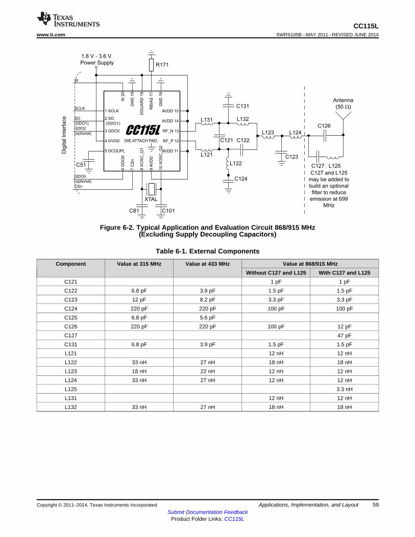
Antenna
(50 )W
Dig
ita
l In
terf
ace
1.8 V - 3.6 V
Power Supply
6 G
DO
0
7 C
Sn
8 X
OS
C_Q
1
9A
VD
D
10 X
OS
C_Q
2
SI 20
GN
D 1
9
DG
UA
RD
18
RB
IAS
17
GN
D 1
6
1 SCLK
2 SO
(GDO1)
3 GDO2
4 DVDD
5 DCOUPL
AVDD 15
AVDD 14
RF_N 13
RF_P 12
AVDD 11
XTAL
C121 C122
L122
L132
C131
L121
L123
C126
R171
C81 C101
C51
CSn
GDO0
(optional)
GDO2
(optional)
SO
(GDO1)
SCLK
SI
CC115LDIE ATTACH PAD:
L131
C124
C123
L124
C127 L125
C127 and L125
may be added to
build an optional
filter to reduce
emission at 699
MHz
CC115Lwww.ti.com SWRS105B –MAY 2011–REVISED JUNE 2014
Figure 6-2. Typical Application and Evaluation Circuit 868/915 MHz(Excluding Supply Decoupling Capacitors)
Table 6-1. External Components
Component Value at 315 MHz Value at 433 MHz Value at 868/915 MHzWithout C127 and L125 With C127 and L125
C121 1 pF 1 pFC122 6.8 pF 3.9 pF 1.5 pF 1.5 pFC123 12 pF 8.2 pF 3.3 pF 3.3 pFC124 220 pF 220 pF 100 pF 100 pFC125 6.8 pF 5.6 pFC126 220 pF 220 pF 100 pF 12 pFC127 47 pFC131 6.8 pF 3.9 pF 1.5 pF 1.5 pFL121 12 nH 12 nHL122 33 nH 27 nH 18 nH 18 nHL123 18 nH 22 nH 12 nH 12 nHL124 33 nH 27 nH 12 nH 12 nHL125 3.3 nHL131 12 nH 12 nHL132 33 nH 27 nH 18 nH 18 nH
Copyright © 2011–2014, Texas Instruments Incorporated Applications, Implementation, and Layout 59Submit Documentation Feedback
Product Folder Links: CC115L
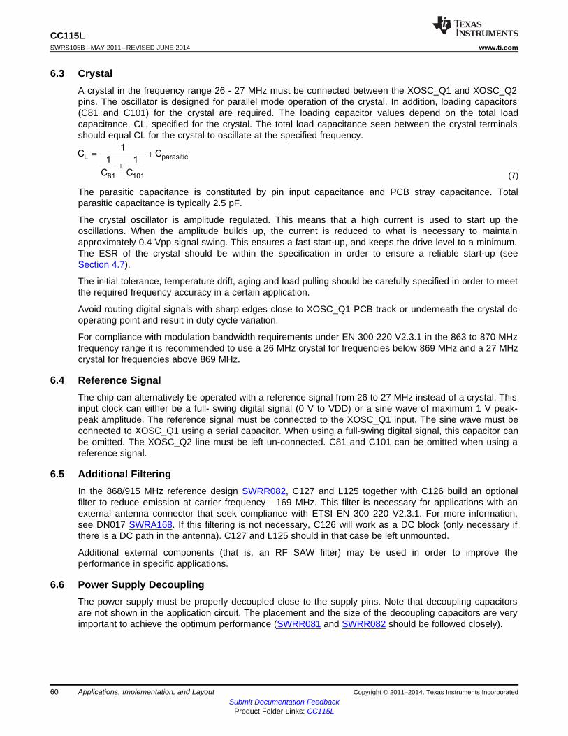
L parasitic
81 101
1C C
1 1
C C
= +
+
CC115LSWRS105B –MAY 2011–REVISED JUNE 2014 www.ti.com
6.3 CrystalA crystal in the frequency range 26 - 27 MHz must be connected between the XOSC_Q1 and XOSC_Q2pins. The oscillator is designed for parallel mode operation of the crystal. In addition, loading capacitors(C81 and C101) for the crystal are required. The loading capacitor values depend on the total loadcapacitance, CL, specified for the crystal. The total load capacitance seen between the crystal terminalsshould equal CL for the crystal to oscillate at the specified frequency.
(7)
The parasitic capacitance is constituted by pin input capacitance and PCB stray capacitance. Totalparasitic capacitance is typically 2.5 pF.
The crystal oscillator is amplitude regulated. This means that a high current is used to start up theoscillations. When the amplitude builds up, the current is reduced to what is necessary to maintainapproximately 0.4 Vpp signal swing. This ensures a fast start-up, and keeps the drive level to a minimum.The ESR of the crystal should be within the specification in order to ensure a reliable start-up (seeSection 4.7).
The initial tolerance, temperature drift, aging and load pulling should be carefully specified in order to meetthe required frequency accuracy in a certain application.
Avoid routing digital signals with sharp edges close to XOSC_Q1 PCB track or underneath the crystal dcoperating point and result in duty cycle variation.
For compliance with modulation bandwidth requirements under EN 300 220 V2.3.1 in the 863 to 870 MHzfrequency range it is recommended to use a 26 MHz crystal for frequencies below 869 MHz and a 27 MHzcrystal for frequencies above 869 MHz.
6.4 Reference SignalThe chip can alternatively be operated with a reference signal from 26 to 27 MHz instead of a crystal. Thisinput clock can either be a full- swing digital signal (0 V to VDD) or a sine wave of maximum 1 V peak-peak amplitude. The reference signal must be connected to the XOSC_Q1 input. The sine wave must beconnected to XOSC_Q1 using a serial capacitor. When using a full-swing digital signal, this capacitor canbe omitted. The XOSC_Q2 line must be left un-connected. C81 and C101 can be omitted when using areference signal.
6.5 Additional FilteringIn the 868/915 MHz reference design SWRR082, C127 and L125 together with C126 build an optionalfilter to reduce emission at carrier frequency - 169 MHz. This filter is necessary for applications with anexternal antenna connector that seek compliance with ETSI EN 300 220 V2.3.1. For more information,see DN017 SWRA168. If this filtering is not necessary, C126 will work as a DC block (only necessary ifthere is a DC path in the antenna). C127 and L125 should in that case be left unmounted.
Additional external components (that is, an RF SAW filter) may be used in order to improve theperformance in specific applications.
6.6 Power Supply DecouplingThe power supply must be properly decoupled close to the supply pins. Note that decoupling capacitorsare not shown in the application circuit. The placement and the size of the decoupling capacitors are veryimportant to achieve the optimum performance (SWRR081 and SWRR082 should be followed closely).
60 Applications, Implementation, and Layout Copyright © 2011–2014, Texas Instruments IncorporatedSubmit Documentation Feedback
Product Folder Links: CC115L

CC115Lwww.ti.com SWRS105B –MAY 2011–REVISED JUNE 2014
6.7 PCB Layout RecommendationsThe top layer should be used for signal routing, and the open areas should be filled with metallizationconnected to ground using several vias.
The area under the chip is used for grounding and shall be connected to the bottom ground plane withseveral vias for good thermal performance and sufficiently low inductance to ground.
In SWRR081 and SWRR082, 5 vias are placed inside the exposed die attached pad. These vias shouldbe “tented” (covered with solder mask) on the component side of the PCB to avoid migration of solderthrough the vias during the solder reflow process.
The solder paste coverage should not be 100%. If it is, out gassing may occur during the reflow process,which may cause defects (splattering, solder balling). Using “tented” vias reduces the solder pastecoverage below 100%. See Figure 6-3 for top solder resist and top paste masks.
Each decoupling capacitor should be placed as close as possible to the supply pin it is supposed todecouple. Each decoupling capacitor should be connected to the power line (or power plane) by separatevias. The best routing is from the power line (or power plane) to the decoupling capacitor and then to theCC115L supply pin. Supply power filtering is very important.
Each decoupling capacitor ground pad should be connected to the ground plane by separate vias. Directconnections between neighboring power pins will increase noise coupling and should be avoided unlessabsolutely necessary. Routing in the ground plane underneath the chip or the balun/RF matching circuit,or between the chip's ground vias and the decoupling capacitor's ground vias should be avoided. Thisimproves the grounding and ensures the shortest possible current return path.
Avoid routing digital signals with sharp edges close to XOSC_Q1 PCB track or underneath the crystal Q1pad as this may shift the crystal dc operating point and result in duty cycle variation.
The external components should ideally be as small as possible (0402 is recommended) and surfacemount devices are highly recommended. Components with different sizes than those specified may havediffering characteristics.
Precaution should be used when placing the microcontroller in order to avoid noise interfering with the RFcircuitry.
A CC11xL Development Kit with a fully assembled CC115L Evaluation Module is available. It is stronglyadvised that this reference layout is followed very closely in order to get the best performance. Theschematic, BOM and layout Gerber files are all available from the TI website (SWRR081 and SWRR082).
Figure 6-3. Left: Top Solder Resist Mask (Negative) – Right: Top Paste Mask. Circles are Vias
Copyright © 2011–2014, Texas Instruments Incorporated Applications, Implementation, and Layout 61Submit Documentation Feedback
Product Folder Links: CC115L

CC115LSWRS105B –MAY 2011–REVISED JUNE 2014 www.ti.com
7 Device and Documentation Support
7.1 Device Support
7.1.1 Device NomenclatureTo designate the stages in the product development cycle, TI assigns prefixes to the part numbers of allmicroprocessors (MPUs) and support tools. Each device has one of three prefixes: X, P, or null (no prefix)(for example, CC115L). Texas Instruments recommends two of three possible prefix designators for itssupport tools: TMDX and TMDS. These prefixes represent evolutionary stages of product developmentfrom engineering prototypes (TMDX) through fully qualified production devices and tools (TMDS).
Device development evolutionary flow:
X Experimental device that is not necessarily representative of the final device's electricalspecifications and may not use production assembly flow.
P Prototype device that is not necessarily the final silicon die and may not necessarily meetfinal electrical specifications.
null Production version of the silicon die that is fully qualified.
Support tool development evolutionary flow:
TMDX Development-support product that has not yet completed Texas Instruments internalqualification testing.
TMDS Fully-qualified development-support product.
X and P devices and TMDX development-support tools are shipped against the following disclaimer:
"Developmental product is intended for internal evaluation purposes."
Production devices and TMDS development-support tools have been characterized fully, and the qualityand reliability of the device have been demonstrated fully. TI's standard warranty applies.
Predictions show that prototype devices (X or P) have a greater failure rate than the standard productiondevices. Texas Instruments recommends that these devices not be used in any production systembecause their expected end-use failure rate still is undefined. Only qualified production devices are to beused.
TI device nomenclature also includes a suffix with the device family name. This suffix indicates thepackage type (for example, RGP) and the temperature range (for example, blank is the defaultcommercial temperature range).
For orderable part numbers of CC115L devices in the QFN package types, see the Package OptionAddendum of this document, the TI website (www.ti.com), or contact your TI sales representative.
62 Device and Documentation Support Copyright © 2011–2014, Texas Instruments IncorporatedSubmit Documentation Feedback
Product Folder Links: CC115L

CC115Lwww.ti.com SWRS105B –MAY 2011–REVISED JUNE 2014
7.2 Documentation Support
7.2.1 Related Documentation from Texas InstrumentsThe following documents describe the CC115L transmitter. Copies of these documents are available onthe Internet at www.ti.com.
SWRR046 Characterization Design 315 - 433 MHz (Identical to the CC1101EM 315 - 433 MHzReference Design)
SWRR045 Characterization Design 868 - 915 MHz (Identical to the CC1101EM 868 - 915 MHzReference Design)
SWRZ036 CC115L Errata Notes
SWRC176 SmartRF Studio
SWRA168 DN017 CC11xx 868/915 MHz RF Matching
SWRA123 DN006 CC11xx Settings for FCC 15.247 Solutions
SWRA168 DN013 Programming Output Power on CC1101
SWRS089 CC1190 Data Sheet
SWRA346 DN032 Options for Cost Optimized CC11xx Matching
SWRR081 CC110LEM / CC115LEM 433 MHz Reference Design
SWRR082 CC110LEM / CC115LEM 868 - 915 MHz Reference Design
7.2.2 Community ResourcesThe following links connect to TI community resources. Linked contents are provided "AS IS" by therespective contributors. They do not constitute TI specifications and do not necessarily reflect TI's views;see TI's Terms of Use.
TI E2E™ Online Community TI's Engineer-to-Engineer (E2E) Community. Created to fostercollaboration among engineers. At e2e.ti.com, you can ask questions, share knowledge,explore ideas and help solve problems with fellow engineers.
TI Embedded Processors Wiki Texas Instruments Embedded Processors Wiki. Established to helpdevelopers get started with Embedded Processors from Texas Instruments and to fosterinnovation and growth of general knowledge about the hardware and software surroundingthese devices.
7.3 TrademarksE2E is a trademark of Texas Instruments.All other trademarks are the property of their respective owners.
Copyright © 2011–2014, Texas Instruments Incorporated Device and Documentation Support 63Submit Documentation Feedback
Product Folder Links: CC115L

CC115LSWRS105B –MAY 2011–REVISED JUNE 2014 www.ti.com
7.4 Electrostatic Discharge CautionThis integrated circuit can be damaged by ESD. Texas Instruments recommends that all integrated circuits be handled withappropriate precautions. Failure to observe proper handling and installation procedures can cause damage.
ESD damage can range from subtle performance degradation to complete device failure. Precision integrated circuits may be moresusceptible to damage because very small parametric changes could cause the device not to meet its published specifications.
7.5 Export Control NoticeRecipient agrees to not knowingly export or re-export, directly or indirectly, any product or technical data(as defined by the U.S., EU, and other Export Administration Regulations) including software, or anycontrolled product restricted by other applicable national regulations, received from Disclosing party underthis Agreement, or any direct product of such technology, to any destination to which such export or re-export is restricted or prohibited by U.S. or other applicable laws, without obtaining prior authorization fromU.S. Department of Commerce and other competent Government authorities to the extent required bythose laws.
7.6 GlossarySLYZ022 — TI Glossary.
This glossary lists and explains terms, acronyms and definitions.
7.7 Additional AcronymsAdditional acronyms used in this data sheet are described below.
2-FSK Binary Frequency Shift Keying
4-FSK Quaternary Frequency Shift Keying
ADC Analog to Digital Converter
AMR Automatic Meter Reading
BOM Bill of Material
BT Bandwidth-Time product
CFR Code of Federal Regulations
CRC Cyclic Redundancy Check
CW Continuous Wave (Unmodulated Carrier)
DC Direct Current
ESR Equivalent Series Resistance
FCC Federal Communications Commission
FIFO First-In-First-Out
FS Frequency Synthesizer
GFSK Gaussian shaped Frequency Shift Keying
IF Intermediate Frequency
I/Q In-Phase/Quadrature
ISM Industrial, Scientific, Medical
LC Inductor-Capacitor
LO Local Oscillator
LSB Least Significant Bit
MCU Microcontroller Unit
64 Device and Documentation Support Copyright © 2011–2014, Texas Instruments IncorporatedSubmit Documentation Feedback
Product Folder Links: CC115L
CC115Lwww.ti.com SWRS105B –MAY 2011–REVISED JUNE 2014
MSB Most Significant Bit
N/A Not Applicable
NRZ Non Return to Zero (Coding)
OOK On-Off Keying
PA Power Amplifier
PCB Printed Circuit Board
PD Power Down
PER Packet Error Rate
PLL Phase Locked Loop
POR Power-On Reset
QLP Quad Leadless Package
QPSK Quadrature Phase Shift Keying
RC Resistor-Capacitor
RF Radio Frequency
SPI Serial Peripheral Interface
SRD Short Range Devices
TX Transmit, Transmit Mode
VCO Voltage Controlled Oscillator
XOSC Crystal Oscillator
XTAL Crystal
Copyright © 2011–2014, Texas Instruments Incorporated Device and Documentation Support 65Submit Documentation Feedback
Product Folder Links: CC115L

CC115LSWRS105B –MAY 2011–REVISED JUNE 2014 www.ti.com
8 Mechanical Packaging and Orderable Information
8.1 Packaging InformationThe following pages include mechanical packaging and orderable information. This information is the mostcurrent data available for the designated devices. This data is subject to change without notice andrevision of this document. For browser-based versions of this data sheet, refer to the left-hand navigation.
66 Mechanical Packaging and Orderable Information Copyright © 2011–2014, Texas Instruments IncorporatedSubmit Documentation Feedback
Product Folder Links: CC115L

PACKAGE OPTION ADDENDUM
www.ti.com 9-Mar-2018
Addendum-Page 1
PACKAGING INFORMATION
Orderable Device Status(1)
Package Type PackageDrawing
Pins PackageQty
Eco Plan(2)
Lead/Ball Finish(6)
MSL Peak Temp(3)
Op Temp (°C) Device Marking(4/5)
Samples
CC115LRGPR ACTIVE QFN RGP 20 3000 Green (RoHS& no Sb/Br)
CU NIPDAU |CU NIPDAUAG
Level-3-260C-168 HR -40 to 85 CC115L
CC115LRGPT ACTIVE QFN RGP 20 250 Green (RoHS& no Sb/Br)
CU NIPDAU |CU NIPDAUAG
Level-3-260C-168 HR -40 to 85 CC115L
(1) The marketing status values are defined as follows:ACTIVE: Product device recommended for new designs.LIFEBUY: TI has announced that the device will be discontinued, and a lifetime-buy period is in effect.NRND: Not recommended for new designs. Device is in production to support existing customers, but TI does not recommend using this part in a new design.PREVIEW: Device has been announced but is not in production. Samples may or may not be available.OBSOLETE: TI has discontinued the production of the device.
(2) RoHS: TI defines "RoHS" to mean semiconductor products that are compliant with the current EU RoHS requirements for all 10 RoHS substances, including the requirement that RoHS substancedo not exceed 0.1% by weight in homogeneous materials. Where designed to be soldered at high temperatures, "RoHS" products are suitable for use in specified lead-free processes. TI mayreference these types of products as "Pb-Free".RoHS Exempt: TI defines "RoHS Exempt" to mean products that contain lead but are compliant with EU RoHS pursuant to a specific EU RoHS exemption.Green: TI defines "Green" to mean the content of Chlorine (Cl) and Bromine (Br) based flame retardants meet JS709B low halogen requirements of <=1000ppm threshold. Antimony trioxide basedflame retardants must also meet the <=1000ppm threshold requirement.
(3) MSL, Peak Temp. - The Moisture Sensitivity Level rating according to the JEDEC industry standard classifications, and peak solder temperature.
(4) There may be additional marking, which relates to the logo, the lot trace code information, or the environmental category on the device.
(5) Multiple Device Markings will be inside parentheses. Only one Device Marking contained in parentheses and separated by a "~" will appear on a device. If a line is indented then it is a continuationof the previous line and the two combined represent the entire Device Marking for that device.
(6) Lead/Ball Finish - Orderable Devices may have multiple material finish options. Finish options are separated by a vertical ruled line. Lead/Ball Finish values may wrap to two lines if the finishvalue exceeds the maximum column width.
Important Information and Disclaimer:The information provided on this page represents TI's knowledge and belief as of the date that it is provided. TI bases its knowledge and belief on informationprovided by third parties, and makes no representation or warranty as to the accuracy of such information. Efforts are underway to better integrate information from third parties. TI has taken andcontinues to take reasonable steps to provide representative and accurate information but may not have conducted destructive testing or chemical analysis on incoming materials and chemicals.TI and TI suppliers consider certain information to be proprietary, and thus CAS numbers and other limited information may not be available for release.
In no event shall TI's liability arising out of such information exceed the total purchase price of the TI part(s) at issue in this document sold by TI to Customer on an annual basis.

PACKAGE OPTION ADDENDUM
www.ti.com 9-Mar-2018
Addendum-Page 2

TAPE AND REEL INFORMATION
*All dimensions are nominal
Device PackageType
PackageDrawing
Pins SPQ ReelDiameter
(mm)
ReelWidth
W1 (mm)
A0(mm)
B0(mm)
K0(mm)
P1(mm)
W(mm)
Pin1Quadrant
CC115LRGPR QFN RGP 20 3000 330.0 12.4 4.3 4.3 1.5 8.0 12.0 Q2
CC115LRGPT QFN RGP 20 250 180.0 12.4 4.3 4.3 1.5 8.0 12.0 Q2
PACKAGE MATERIALS INFORMATION
www.ti.com 21-Nov-2016
Pack Materials-Page 1

*All dimensions are nominal
Device Package Type Package Drawing Pins SPQ Length (mm) Width (mm) Height (mm)
CC115LRGPR QFN RGP 20 3000 336.6 336.6 28.6
CC115LRGPT QFN RGP 20 250 210.0 185.0 35.0
PACKAGE MATERIALS INFORMATION
www.ti.com 21-Nov-2016
Pack Materials-Page 2
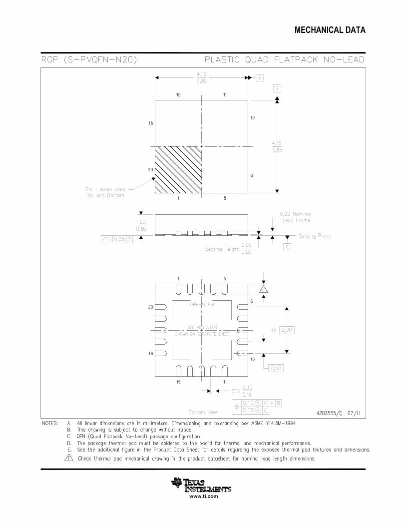

IMPORTANT NOTICE
Texas Instruments Incorporated (TI) reserves the right to make corrections, enhancements, improvements and other changes to itssemiconductor products and services per JESD46, latest issue, and to discontinue any product or service per JESD48, latest issue. Buyersshould obtain the latest relevant information before placing orders and should verify that such information is current and complete.TI’s published terms of sale for semiconductor products (http://www.ti.com/sc/docs/stdterms.htm) apply to the sale of packaged integratedcircuit products that TI has qualified and released to market. Additional terms may apply to the use or sale of other types of TI products andservices.Reproduction of significant portions of TI information in TI data sheets is permissible only if reproduction is without alteration and isaccompanied by all associated warranties, conditions, limitations, and notices. TI is not responsible or liable for such reproduceddocumentation. Information of third parties may be subject to additional restrictions. Resale of TI products or services with statementsdifferent from or beyond the parameters stated by TI for that product or service voids all express and any implied warranties for theassociated TI product or service and is an unfair and deceptive business practice. TI is not responsible or liable for any such statements.Buyers and others who are developing systems that incorporate TI products (collectively, “Designers”) understand and agree that Designersremain responsible for using their independent analysis, evaluation and judgment in designing their applications and that Designers havefull and exclusive responsibility to assure the safety of Designers' applications and compliance of their applications (and of all TI productsused in or for Designers’ applications) with all applicable regulations, laws and other applicable requirements. Designer represents that, withrespect to their applications, Designer has all the necessary expertise to create and implement safeguards that (1) anticipate dangerousconsequences of failures, (2) monitor failures and their consequences, and (3) lessen the likelihood of failures that might cause harm andtake appropriate actions. Designer agrees that prior to using or distributing any applications that include TI products, Designer willthoroughly test such applications and the functionality of such TI products as used in such applications.TI’s provision of technical, application or other design advice, quality characterization, reliability data or other services or information,including, but not limited to, reference designs and materials relating to evaluation modules, (collectively, “TI Resources”) are intended toassist designers who are developing applications that incorporate TI products; by downloading, accessing or using TI Resources in anyway, Designer (individually or, if Designer is acting on behalf of a company, Designer’s company) agrees to use any particular TI Resourcesolely for this purpose and subject to the terms of this Notice.TI’s provision of TI Resources does not expand or otherwise alter TI’s applicable published warranties or warranty disclaimers for TIproducts, and no additional obligations or liabilities arise from TI providing such TI Resources. TI reserves the right to make corrections,enhancements, improvements and other changes to its TI Resources. TI has not conducted any testing other than that specificallydescribed in the published documentation for a particular TI Resource.Designer is authorized to use, copy and modify any individual TI Resource only in connection with the development of applications thatinclude the TI product(s) identified in such TI Resource. NO OTHER LICENSE, EXPRESS OR IMPLIED, BY ESTOPPEL OR OTHERWISETO ANY OTHER TI INTELLECTUAL PROPERTY RIGHT, AND NO LICENSE TO ANY TECHNOLOGY OR INTELLECTUAL PROPERTYRIGHT OF TI OR ANY THIRD PARTY IS GRANTED HEREIN, including but not limited to any patent right, copyright, mask work right, orother intellectual property right relating to any combination, machine, or process in which TI products or services are used. Informationregarding or referencing third-party products or services does not constitute a license to use such products or services, or a warranty orendorsement thereof. Use of TI Resources may require a license from a third party under the patents or other intellectual property of thethird party, or a license from TI under the patents or other intellectual property of TI.TI RESOURCES ARE PROVIDED “AS IS” AND WITH ALL FAULTS. TI DISCLAIMS ALL OTHER WARRANTIES ORREPRESENTATIONS, EXPRESS OR IMPLIED, REGARDING RESOURCES OR USE THEREOF, INCLUDING BUT NOT LIMITED TOACCURACY OR COMPLETENESS, TITLE, ANY EPIDEMIC FAILURE WARRANTY AND ANY IMPLIED WARRANTIES OFMERCHANTABILITY, FITNESS FOR A PARTICULAR PURPOSE, AND NON-INFRINGEMENT OF ANY THIRD PARTY INTELLECTUALPROPERTY RIGHTS. TI SHALL NOT BE LIABLE FOR AND SHALL NOT DEFEND OR INDEMNIFY DESIGNER AGAINST ANY CLAIM,INCLUDING BUT NOT LIMITED TO ANY INFRINGEMENT CLAIM THAT RELATES TO OR IS BASED ON ANY COMBINATION OFPRODUCTS EVEN IF DESCRIBED IN TI RESOURCES OR OTHERWISE. IN NO EVENT SHALL TI BE LIABLE FOR ANY ACTUAL,DIRECT, SPECIAL, COLLATERAL, INDIRECT, PUNITIVE, INCIDENTAL, CONSEQUENTIAL OR EXEMPLARY DAMAGES INCONNECTION WITH OR ARISING OUT OF TI RESOURCES OR USE THEREOF, AND REGARDLESS OF WHETHER TI HAS BEENADVISED OF THE POSSIBILITY OF SUCH DAMAGES.Unless TI has explicitly designated an individual product as meeting the requirements of a particular industry standard (e.g., ISO/TS 16949and ISO 26262), TI is not responsible for any failure to meet such industry standard requirements.Where TI specifically promotes products as facilitating functional safety or as compliant with industry functional safety standards, suchproducts are intended to help enable customers to design and create their own applications that meet applicable functional safety standardsand requirements. Using products in an application does not by itself establish any safety features in the application. Designers mustensure compliance with safety-related requirements and standards applicable to their applications. Designer may not use any TI products inlife-critical medical equipment unless authorized officers of the parties have executed a special contract specifically governing such use.Life-critical medical equipment is medical equipment where failure of such equipment would cause serious bodily injury or death (e.g., lifesupport, pacemakers, defibrillators, heart pumps, neurostimulators, and implantables). Such equipment includes, without limitation, allmedical devices identified by the U.S. Food and Drug Administration as Class III devices and equivalent classifications outside the U.S.TI may expressly designate certain products as completing a particular qualification (e.g., Q100, Military Grade, or Enhanced Product).Designers agree that it has the necessary expertise to select the product with the appropriate qualification designation for their applicationsand that proper product selection is at Designers’ own risk. Designers are solely responsible for compliance with all legal and regulatoryrequirements in connection with such selection.Designer will fully indemnify TI and its representatives against any damages, costs, losses, and/or liabilities arising out of Designer’s non-compliance with the terms and provisions of this Notice.
Mailing Address: Texas Instruments, Post Office Box 655303, Dallas, Texas 75265Copyright © 2018, Texas Instruments Incorporated