TPS53622 Dual-Channel (1-Phase + 1-Phase) or (2 …€¢ Conversion Voltage Range: 4.5 V to 17 V •...
16
Product Folder Order Now Technical Documents Tools & Software Support & Community An IMPORTANT NOTICE at the end of this data sheet addresses availability, warranty, changes, use in safety-critical applications, intellectual property matters and other important disclaimers. PRODUCTION DATA. TPS53622 SLUSD41 – NOVEMBER 2016 TPS53622 Dual-Channel (1-Phase + 1-Phase) or (2-Phase + 0-Phase) D-CAP+™ Step-Down Multiphase Controller with NVM and PMBus™ for VR13 Server V CCIO +V MCP 1 Device Overview 1 1.1 Features 1 • Intel VR13 Serial VID (SVID) Compliant • Full VR13 Server Feature Set Including Digital Input Power Monitor • Programmable Loop Compensations • Configurable with Non-Volatile Memory (NVM) for Low External Component Counts • Individual Phase Current Calibrations and Reports • Dynamic Phase Shedding with Programmable Current Threshold for Optimizing Efficiency at Light and Heavy Loads • Fast Phase-Adding for Undershoot Reduction (USR) • Backward VR12.0 and VR12.5 Compatible • 8-Bit DAC with Selectable 5 mV or 10 mV Resolution and Output Ranges from 0.25 V to 1.52 V or 0.5 to 2.8125 V for Dual Channels • Driverless Configuration for Efficient High- Frequency Switching • Fully Compatible with TI NextFET™ Power Stage for High-Density Solutions • Accurate, Adjustable Voltage Positioning • Patented AutoBalance™ Phase Balancing • Selectable, 16-level Per-Phase Current Limit • PMBus™ System Interface for Telemetry of Voltage, Current, Power, Temperature, and Fault Conditions • Dynamic Output Voltage Transitions with Programmable Slew Rates via SVID or PMBus Interface • Conversion Voltage Range: 4.5 V to 17 V • Low Quiescent Current 1.2 Applications • ASIC Needs Dual Power Rails • High-Performance Processor Power (1) For more information, see, Mechanical, Packaging, and Orderable Information. 1.3 Description The TPS53622 is a fully VR13 SVID compliant step-down controller with dual channels, built-in non- volatile memory (NVM), and PMBus™ interface, and is fully compatible with TI NexFET ™power stage. Advanced control features such as D-CAP+™ architecture with undershoot reduction (USR) provide fast transient response, low output capacitance, and good current sharing. The device also provides novel phase interleaving strategy and dynamic phase shedding for efficiency improvement at different loads. Adjustable control of V CORE slew rate and voltage positioning round out the Intel ® VR13™ features. In addition, the device supports the PMBus communication interface for reporting the telemetry of voltage, current, power, temperature, and fault conditions to the systems. All programmable parameters can be configured by the PMBus interface and can be stored in NVM as the new default values to minimize the external component count. The TPS53622 device if offered in a thermally enhanced -pin QFN packaged and is rated to operate from –40°C to 125°C. Table 1-1. Device Information (1) PART NUMBER PACKAGE BODY SIZE TPS53622 QFN (40) 5 mm × 5 mm
Transcript of TPS53622 Dual-Channel (1-Phase + 1-Phase) or (2 …€¢ Conversion Voltage Range: 4.5 V to 17 V •...

Product
Folder
Order
Now
Technical
Documents
Tools &
Software
Support &Community
An IMPORTANT NOTICE at the end of this data sheet addresses availability, warranty, changes, use in safety-critical applications,intellectual property matters and other important disclaimers. PRODUCTION DATA.
TPS53622SLUSD41 –NOVEMBER 2016
TPS53622 Dual-Channel (1-Phase + 1-Phase) or (2-Phase + 0-Phase) D-CAP+™ Step-DownMultiphase Controller
with NVM and PMBus™ for VR13 Server VCCIO + VMCP
1 Device Overview
1
1.1 Features1
• Intel VR13 Serial VID (SVID) Compliant• Full VR13 Server Feature Set Including Digital
Input Power Monitor• Programmable Loop Compensations• Configurable with Non-Volatile Memory (NVM) for
Low External Component Counts• Individual Phase Current Calibrations and Reports• Dynamic Phase Shedding with Programmable
Current Threshold for Optimizing Efficiency at Lightand Heavy Loads
• Fast Phase-Adding for Undershoot Reduction(USR)
• Backward VR12.0 and VR12.5 Compatible• 8-Bit DAC with Selectable 5 mV or 10 mV
Resolution and Output Ranges from 0.25 V to1.52 V or 0.5 to 2.8125 V for Dual Channels
• Driverless Configuration for Efficient High-Frequency Switching
• Fully Compatible with TI NextFET™ Power Stagefor High-Density Solutions
• Accurate, Adjustable Voltage Positioning• Patented AutoBalance™ Phase Balancing• Selectable, 16-level Per-Phase Current Limit• PMBus™ System Interface for Telemetry of
Voltage, Current, Power, Temperature, and FaultConditions
• Dynamic Output Voltage Transitions withProgrammable Slew Rates via SVID or PMBusInterface
• Conversion Voltage Range: 4.5 V to 17 V• Low Quiescent Current
1.2 Applications• ASIC Needs Dual Power Rails • High-Performance Processor Power
(1) For more information, see, Mechanical, Packaging, and Orderable Information.
1.3 DescriptionThe TPS53622 is a fully VR13 SVID compliant step-down controller with dual channels, built-in non-volatile memory (NVM), and PMBus™ interface, and is fully compatible with TI NexFET ™power stage.Advanced control features such as D-CAP+™ architecture with undershoot reduction (USR) provide fasttransient response, low output capacitance, and good current sharing. The device also provides novelphase interleaving strategy and dynamic phase shedding for efficiency improvement at different loads.Adjustable control of VCORE slew rate and voltage positioning round out the Intel® VR13™ features. Inaddition, the device supports the PMBus communication interface for reporting the telemetry of voltage,current, power, temperature, and fault conditions to the systems. All programmable parameters can beconfigured by the PMBus interface and can be stored in NVM as the new default values to minimize theexternal component count.
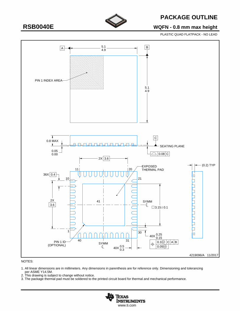
The TPS53622 device if offered in a thermally enhanced -pin QFN packaged and is rated to operate from–40°C to 125°C.
Table 1-1. Device Information (1)
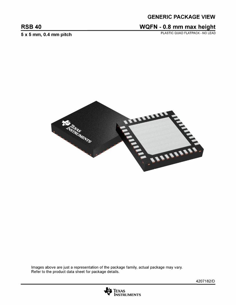
PART NUMBER PACKAGE BODY SIZETPS53622 QFN (40) 5 mm × 5 mm

2
TPS53622SLUSD41 –NOVEMBER 2016 www.ti.com
Submit Documentation FeedbackProduct Folder Links: TPS53622
Revision History Copyright © 2016, Texas Instruments Incorporated
Table of Contents1 Device Overview ......................................... 1
1.1 Features .............................................. 11.2 Applications........................................... 11.3 Description............................................ 1
2 Revision History ......................................... 23 Device and Documentation Support ................. 3
3.1 Receiving Notification of Documentation Updates ... 33.2 Community Resources ............................... 33.3 Trademarks ........................................... 33.4 Electrostatic Discharge Caution ...................... 33.5 Glossary .............................................. 3
4 Mechanical, Packaging, and OrderableInformation ................................................ 3
2 Revision HistoryNOTE: Page numbers for previous revisions may differ from page numbers in the current version.
DATE REVISION NOTESNovember 2016 * Initial release.

3
TPS53622www.ti.com SLUSD41 –NOVEMBER 2016
Submit Documentation FeedbackProduct Folder Links: TPS53622
Mechanical, Packaging, and Orderable InformationCopyright © 2016, Texas Instruments Incorporated
3 Device and Documentation Support
3.1 Receiving Notification of Documentation UpdatesTo receive notification of documentation updates, navigate to the device product folder on ti.com. In theupper right corner, click on Alert me to register and receive a weekly digest of any product information thathas changed. For change details, review the revision history included in any revised document.
3.2 Community ResourcesThe following links connect to TI community resources. Linked contents are provided "AS IS" by therespective contributors. They do not constitute TI specifications and do not necessarily reflect TI's views;see TI's Terms of Use.TI E2E™ Online Community TI's Engineer-to-Engineer (E2E) Community. Created to foster
collaboration among engineers. At e2e.ti.com, you can ask questions, share knowledge,explore ideas and help solve problems with fellow engineers.
Design Support TI's Design Support Quickly find helpful E2E forums along with design support toolsand contact information for technical support.
3.3 TrademarksNextFET, AutoBalance, PMBus, NexFET, D-CAP+, E2E are trademarks of Texas Instruments.VR13 is a trademark of Intel.Intel is a registered trademark of Intel.PMBus is a trademark of SMIF, Inc..
3.4 Electrostatic Discharge CautionThis integrated circuit can be damaged by ESD. Texas Instruments recommends that all integrated circuits be handled withappropriate precautions. Failure to observe proper handling and installation procedures can cause damage.
ESD damage can range from subtle performance degradation to complete device failure. Precision integrated circuits may be moresusceptible to damage because very small parametric changes could cause the device not to meet its published specifications.
3.5 GlossarySLYZ022 — TI Glossary.
This glossary lists and explains terms, acronyms, and definitions.
4 Mechanical, Packaging, and Orderable Information
The following pages include mechanical, packaging, and orderable information. This information is themost current data available for the designated devices. This data is subject to change without notice andrevision of this document. For browser-based versions of this data sheet, refer to the left-hand navigation.

PACKAGE OPTION ADDENDUM
www.ti.com 31-Mar-2018
Addendum-Page 1
PACKAGING INFORMATION
Orderable Device Status(1)
Package Type PackageDrawing
Pins PackageQty
Eco Plan(2)
Lead/Ball Finish(6)
MSL Peak Temp(3)
Op Temp (°C) Device Marking(4/5)
Samples
TPS53622RSBR ACTIVE WQFN RSB 40 3000 Green (RoHS& no Sb/Br)
CU NIPDAUAG Level-2-260C-1 YEAR -40 to 125 TPS53622
TPS53622RSBT ACTIVE WQFN RSB 40 250 Green (RoHS& no Sb/Br)
CU NIPDAU |CU NIPDAUAG
Level-2-260C-1 YEAR -40 to 125 TPS53622
(1) The marketing status values are defined as follows:ACTIVE: Product device recommended for new designs.LIFEBUY: TI has announced that the device will be discontinued, and a lifetime-buy period is in effect.NRND: Not recommended for new designs. Device is in production to support existing customers, but TI does not recommend using this part in a new design.PREVIEW: Device has been announced but is not in production. Samples may or may not be available.OBSOLETE: TI has discontinued the production of the device.
(2) RoHS: TI defines "RoHS" to mean semiconductor products that are compliant with the current EU RoHS requirements for all 10 RoHS substances, including the requirement that RoHS substancedo not exceed 0.1% by weight in homogeneous materials. Where designed to be soldered at high temperatures, "RoHS" products are suitable for use in specified lead-free processes. TI mayreference these types of products as "Pb-Free".RoHS Exempt: TI defines "RoHS Exempt" to mean products that contain lead but are compliant with EU RoHS pursuant to a specific EU RoHS exemption.Green: TI defines "Green" to mean the content of Chlorine (Cl) and Bromine (Br) based flame retardants meet JS709B low halogen requirements of <=1000ppm threshold. Antimony trioxide basedflame retardants must also meet the <=1000ppm threshold requirement.
(3) MSL, Peak Temp. - The Moisture Sensitivity Level rating according to the JEDEC industry standard classifications, and peak solder temperature.
(4) There may be additional marking, which relates to the logo, the lot trace code information, or the environmental category on the device.
(5) Multiple Device Markings will be inside parentheses. Only one Device Marking contained in parentheses and separated by a "~" will appear on a device. If a line is indented then it is a continuationof the previous line and the two combined represent the entire Device Marking for that device.
(6) Lead/Ball Finish - Orderable Devices may have multiple material finish options. Finish options are separated by a vertical ruled line. Lead/Ball Finish values may wrap to two lines if the finishvalue exceeds the maximum column width.
Important Information and Disclaimer:The information provided on this page represents TI's knowledge and belief as of the date that it is provided. TI bases its knowledge and belief on informationprovided by third parties, and makes no representation or warranty as to the accuracy of such information. Efforts are underway to better integrate information from third parties. TI has taken andcontinues to take reasonable steps to provide representative and accurate information but may not have conducted destructive testing or chemical analysis on incoming materials and chemicals.TI and TI suppliers consider certain information to be proprietary, and thus CAS numbers and other limited information may not be available for release.
In no event shall TI's liability arising out of such information exceed the total purchase price of the TI part(s) at issue in this document sold by TI to Customer on an annual basis.

PACKAGE OPTION ADDENDUM
www.ti.com 31-Mar-2018
Addendum-Page 2

TAPE AND REEL INFORMATION
*All dimensions are nominal
Device PackageType
PackageDrawing
Pins SPQ ReelDiameter
(mm)
ReelWidth
W1 (mm)
A0(mm)
B0(mm)
K0(mm)
P1(mm)
W(mm)
Pin1Quadrant
TPS53622RSBR WQFN RSB 40 3000 330.0 12.4 5.3 5.3 1.1 8.0 12.0 Q2
TPS53622RSBT WQFN RSB 40 250 180.0 12.4 5.3 5.3 1.1 8.0 12.0 Q2
PACKAGE MATERIALS INFORMATION
www.ti.com 21-Sep-2017
Pack Materials-Page 1

*All dimensions are nominal
Device Package Type Package Drawing Pins SPQ Length (mm) Width (mm) Height (mm)
TPS53622RSBR WQFN RSB 40 3000 367.0 367.0 35.0
TPS53622RSBT WQFN RSB 40 250 210.0 185.0 35.0
PACKAGE MATERIALS INFORMATION
www.ti.com 21-Sep-2017
Pack Materials-Page 2

www.ti.com
PACKAGE OUTLINE
C
40X 0.250.15
40X 0.50.3
0.8 MAX
(0.2) TYP
0.050.00
36X 0.4
2X3.6
2X 3.6
3.15 0.1
A 5.14.9
B
5.14.9
WQFN - 0.8 mm max heightRSB0040EPLASTIC QUAD FLATPACK - NO LEAD
4219096/A 11/2017
PIN 1 INDEX AREA
0.08 C
SEATING PLANE
1
10 21
30
11 20
40 31(OPTIONAL)
PIN 1 ID 0.1 C A B0.05
EXPOSEDTHERMAL PAD
41
SYMM
SYMM
NOTES: 1. All linear dimensions are in millimeters. Any dimensions in parenthesis are for reference only. Dimensioning and tolerancing per ASME Y14.5M. 2. This drawing is subject to change without notice. 3. The package thermal pad must be soldered to the printed circuit board for thermal and mechanical performance.
SCALE 2.700

www.ti.com
EXAMPLE BOARD LAYOUT
0.05 MINALL AROUND
0.05 MAXALL AROUND
40X (0.2)
40X (0.6)
( 0.2) TYPVIA
36X (0.4)
(4.8)
(4.8)
(1.325)
( 3.15)
(R0.05)TYP
(1.325)
WQFN - 0.8 mm max heightRSB0040EPLASTIC QUAD FLATPACK - NO LEAD
4219096/A 11/2017
SYMM
1
10
11 20
21
30
3140
SYMM
LAND PATTERN EXAMPLEEXPOSED METAL SHOWN
SCALE:15X
41
NOTES: (continued) 4. This package is designed to be soldered to a thermal pad on the board. For more information, see Texas Instruments literature number SLUA271 (www.ti.com/lit/slua271).5. Vias are optional depending on application, refer to device data sheet. If any vias are implemented, refer to their locations shown on this view. It is recommended that vias under paste be filled, plugged or tented.
SOLDER MASKOPENING
METAL UNDERSOLDER MASK
SOLDER MASKDEFINED
EXPOSEDMETAL
METAL
SOLDER MASKOPENING
SOLDER MASK DETAILS
NON SOLDER MASKDEFINED
(PREFERRED)
EXPOSEDMETAL

www.ti.com
EXAMPLE STENCIL DESIGN
40X (0.6)
40X (0.2)
36X (0.4)
(4.8)
(4.8)
4X ( 1.37)
(0.785)
(R0.05) TYP
(0.785)
WQFN - 0.8 mm max heightRSB0040EPLASTIC QUAD FLATPACK - NO LEAD
4219096/A 11/2017
NOTES: (continued) 6. Laser cutting apertures with trapezoidal walls and rounded corners may offer better paste release. IPC-7525 may have alternate design recommendations.
SYMM
METALTYP
SOLDER PASTE EXAMPLEBASED ON 0.1 mm THICK STENCIL
EXPOSED PAD 41
75% PRINTED SOLDER COVERAGE BY AREA UNDER PACKAGESCALE:20X
SYMM
1
10
11 20
21
30
3140
41

IMPORTANT NOTICE
Texas Instruments Incorporated (TI) reserves the right to make corrections, enhancements, improvements and other changes to itssemiconductor products and services per JESD46, latest issue, and to discontinue any product or service per JESD48, latest issue. Buyersshould obtain the latest relevant information before placing orders and should verify that such information is current and complete.TI’s published terms of sale for semiconductor products (http://www.ti.com/sc/docs/stdterms.htm) apply to the sale of packaged integratedcircuit products that TI has qualified and released to market. Additional terms may apply to the use or sale of other types of TI products andservices.Reproduction of significant portions of TI information in TI data sheets is permissible only if reproduction is without alteration and isaccompanied by all associated warranties, conditions, limitations, and notices. TI is not responsible or liable for such reproduceddocumentation. Information of third parties may be subject to additional restrictions. Resale of TI products or services with statementsdifferent from or beyond the parameters stated by TI for that product or service voids all express and any implied warranties for theassociated TI product or service and is an unfair and deceptive business practice. TI is not responsible or liable for any such statements.Buyers and others who are developing systems that incorporate TI products (collectively, “Designers”) understand and agree that Designersremain responsible for using their independent analysis, evaluation and judgment in designing their applications and that Designers havefull and exclusive responsibility to assure the safety of Designers' applications and compliance of their applications (and of all TI productsused in or for Designers’ applications) with all applicable regulations, laws and other applicable requirements. Designer represents that, withrespect to their applications, Designer has all the necessary expertise to create and implement safeguards that (1) anticipate dangerousconsequences of failures, (2) monitor failures and their consequences, and (3) lessen the likelihood of failures that might cause harm andtake appropriate actions. Designer agrees that prior to using or distributing any applications that include TI products, Designer willthoroughly test such applications and the functionality of such TI products as used in such applications.TI’s provision of technical, application or other design advice, quality characterization, reliability data or other services or information,including, but not limited to, reference designs and materials relating to evaluation modules, (collectively, “TI Resources”) are intended toassist designers who are developing applications that incorporate TI products; by downloading, accessing or using TI Resources in anyway, Designer (individually or, if Designer is acting on behalf of a company, Designer’s company) agrees to use any particular TI Resourcesolely for this purpose and subject to the terms of this Notice.TI’s provision of TI Resources does not expand or otherwise alter TI’s applicable published warranties or warranty disclaimers for TIproducts, and no additional obligations or liabilities arise from TI providing such TI Resources. TI reserves the right to make corrections,enhancements, improvements and other changes to its TI Resources. TI has not conducted any testing other than that specificallydescribed in the published documentation for a particular TI Resource.Designer is authorized to use, copy and modify any individual TI Resource only in connection with the development of applications thatinclude the TI product(s) identified in such TI Resource. NO OTHER LICENSE, EXPRESS OR IMPLIED, BY ESTOPPEL OR OTHERWISETO ANY OTHER TI INTELLECTUAL PROPERTY RIGHT, AND NO LICENSE TO ANY TECHNOLOGY OR INTELLECTUAL PROPERTYRIGHT OF TI OR ANY THIRD PARTY IS GRANTED HEREIN, including but not limited to any patent right, copyright, mask work right, orother intellectual property right relating to any combination, machine, or process in which TI products or services are used. Informationregarding or referencing third-party products or services does not constitute a license to use such products or services, or a warranty orendorsement thereof. Use of TI Resources may require a license from a third party under the patents or other intellectual property of thethird party, or a license from TI under the patents or other intellectual property of TI.TI RESOURCES ARE PROVIDED “AS IS” AND WITH ALL FAULTS. TI DISCLAIMS ALL OTHER WARRANTIES ORREPRESENTATIONS, EXPRESS OR IMPLIED, REGARDING RESOURCES OR USE THEREOF, INCLUDING BUT NOT LIMITED TOACCURACY OR COMPLETENESS, TITLE, ANY EPIDEMIC FAILURE WARRANTY AND ANY IMPLIED WARRANTIES OFMERCHANTABILITY, FITNESS FOR A PARTICULAR PURPOSE, AND NON-INFRINGEMENT OF ANY THIRD PARTY INTELLECTUALPROPERTY RIGHTS. TI SHALL NOT BE LIABLE FOR AND SHALL NOT DEFEND OR INDEMNIFY DESIGNER AGAINST ANY CLAIM,INCLUDING BUT NOT LIMITED TO ANY INFRINGEMENT CLAIM THAT RELATES TO OR IS BASED ON ANY COMBINATION OFPRODUCTS EVEN IF DESCRIBED IN TI RESOURCES OR OTHERWISE. IN NO EVENT SHALL TI BE LIABLE FOR ANY ACTUAL,DIRECT, SPECIAL, COLLATERAL, INDIRECT, PUNITIVE, INCIDENTAL, CONSEQUENTIAL OR EXEMPLARY DAMAGES INCONNECTION WITH OR ARISING OUT OF TI RESOURCES OR USE THEREOF, AND REGARDLESS OF WHETHER TI HAS BEENADVISED OF THE POSSIBILITY OF SUCH DAMAGES.Unless TI has explicitly designated an individual product as meeting the requirements of a particular industry standard (e.g., ISO/TS 16949and ISO 26262), TI is not responsible for any failure to meet such industry standard requirements.Where TI specifically promotes products as facilitating functional safety or as compliant with industry functional safety standards, suchproducts are intended to help enable customers to design and create their own applications that meet applicable functional safety standardsand requirements. Using products in an application does not by itself establish any safety features in the application. Designers mustensure compliance with safety-related requirements and standards applicable to their applications. Designer may not use any TI products inlife-critical medical equipment unless authorized officers of the parties have executed a special contract specifically governing such use.Life-critical medical equipment is medical equipment where failure of such equipment would cause serious bodily injury or death (e.g., lifesupport, pacemakers, defibrillators, heart pumps, neurostimulators, and implantables). Such equipment includes, without limitation, allmedical devices identified by the U.S. Food and Drug Administration as Class III devices and equivalent classifications outside the U.S.TI may expressly designate certain products as completing a particular qualification (e.g., Q100, Military Grade, or Enhanced Product).Designers agree that it has the necessary expertise to select the product with the appropriate qualification designation for their applicationsand that proper product selection is at Designers’ own risk. Designers are solely responsible for compliance with all legal and regulatoryrequirements in connection with such selection.Designer will fully indemnify TI and its representatives against any damages, costs, losses, and/or liabilities arising out of Designer’s non-compliance with the terms and provisions of this Notice.
Mailing Address: Texas Instruments, Post Office Box 655303, Dallas, Texas 75265Copyright © 2018, Texas Instruments Incorporated