Dual Single-Phase PWM Controller for CPU and GPU Core ... · Dual Single-Phase PWM Controller for...
40
RT8172A ® DS8172A-00 November 2013 www.richtek.com 1 © Copyright 2013 Richtek Technology Corporation. All rights reserved. is a registered trademark of Richtek Technology Corporation. General Description The RT8172A is a dual single-phase PWM controller with integrated MOSFET drivers, compliant with Intel IMVP7 Pulse Width Modulation Specification to support both CPU core and GPU core power. This part adopts G-NAVP TM (Green-Native AVP), which is Richtek's proprietary topology derived from finite DC gain compensator in constant on- time control mode. The G-NAVP TM makes this part an easy setting PWM controller to meet all Intel AVP (Active Voltage Positioning) mobile CPU/GPU requirements. The RT8172A uses SVID interface to control an 8-bit DAC for output voltage programming. The built-in high accuracy DAC converts the received VID code into a voltage value ranging from 0V to 1.52V with 5mV step voltage. The system accuracy of the controller can reach 0.8%. The RT8172A operates in continuous conduction mode or diode emulation mode, according to the SVID command. The maximum efficiency can reach up to 90% in different operating modes according to different load conditions. The droop function (load line) can be easily programmed by setting the DC gain of the error amplifier. With proper compensation, the load transient response can achieve optimized AVP performance. The output voltage transition slew rate is set via the SVID interface. The RT8172A supports both DCR and sense resistor current sensing. The RT8172A provides VR_READY and thermal throttling output signals for IMVP7 CPU and GPU core. This part also features complete fault protection functions including over-voltage, under-voltage, negative-voltage, over-current and thermal shutdown. Dual Single-Phase PWM Controller for CPU and GPU Core Power Supply Features Dual Single-Phase PWM Controller for CPU Core and GPU Core Power IMVP7 Compatible Power Management States Serial VID Interface G-NAVP TM Topology AVP for CPU VR Only 0.5% DAC Accuracy 0.8% System Accuracy Differential Remote Voltage Sensing Built-in ADC for Platform Programming SETINI/SETINIA for CPU/GPU Core VR Initial Startup Voltage TMPMAX to Set Platform Maximum Temperature ICCMAX/ICCMAXA for CPU/GPU Core VR Maximum Current Power Good Indicator : VR_READY/VRA_READY for CPU/GPU Core Power Thermal Throttling Indicator : VRHOT Diode Emulation Mode at Light Load Condition Fast Line/Load Transient Response Switching Frequency up to 1MHz per Phase OVP, UVP, NVP, OTP, UVLO, OCP RoHS Compliant and Halogen Free RT8172A MOSFET V CORE PHASEA PHASE MOSFET V GPU ALERT ALERT VRHOT VRHOT VR_READY VR_READY VRA_READY VRA_READY VCLK VCLK VDIO VDIO Simplified Application Circuit The RT8172A is available in the WQFN-40L 5x5 small footprint package.
Transcript of Dual Single-Phase PWM Controller for CPU and GPU Core ... · Dual Single-Phase PWM Controller for...

RT8172A®
DS8172A-00 November 2013 www.richtek.com1
©Copyright 2013 Richtek Technology Corporation. All rights reserved. is a registered trademark of Richtek Technology Corporation.
General Description
The RT8172A is a dual single-phase PWM controller with
integrated MOSFET drivers, compliant with Intel IMVP7
Pulse Width Modulation Specification to support both
CPU core and GPU core power. This part adopts G-NAVPTM
(Green-Native AVP), which is Richtek's proprietary topology
derived from finite DC gain compensator in constant on-
time control mode. The G-NAVPTM makes this part an
easy setting PWM controller to meet all Intel AVP (Active
Voltage Positioning) mobile CPU/GPU requirements. The
RT8172A uses SVID interface to control an 8-bit DAC for
output voltage programming. The built-in high accuracy
DAC converts the received VID code into a voltage value
ranging from 0V to 1.52V with 5mV step voltage. The
system accuracy of the controller can reach 0.8%. The
RT8172A operates in continuous conduction mode or
diode emulation mode, according to the SVID command.
The maximum efficiency can reach up to 90% in different
operating modes according to different load conditions.
The droop function (load line) can be easily programmed
by setting the DC gain of the error amplifier. With proper
compensation, the load transient response can achieve
optimized AVP performance.
The output voltage transition slew rate is set via the SVID
interface. The RT8172A supports both DCR and sense
resistor current sensing. The RT8172A provides
VR_READY and thermal throttling output signals for
IMVP7 CPU and GPU core. This part also features
complete fault protection functions including over-voltage,
under-voltage, negative-voltage, over-current and thermal
shutdown.
Dual Single-Phase PWM Controller for CPU and GPU CorePower Supply
Features Dual Single-Phase PWM Controller for CPU Core
and GPU Core Power
IMVP7 Compatible Power Management States
Serial VID Interface
G-NAVPTM Topology
AVP for CPU VR Only
0.5% DAC Accuracy
0.8% System Accuracy
Differential Remote Voltage Sensing
Built-in ADC for Platform Programming
SETINI/SETINIA for CPU/GPU Core VR Initial
Startup Voltage
TMPMAX to Set Platform Maximum Temperature
ICCMAX/ICCMAXA for CPU/GPU Core VR
Maximum Current
Power Good Indicator : VR_READY/VRA_READY for
CPU/GPU Core Power
Thermal Throttling Indicator : VRHOT
Diode Emulation Mode at Light Load Condition
Fast Line/Load Transient Response
Switching Frequency up to 1MHz per Phase
OVP, UVP, NVP, OTP, UVLO, OCP
RoHS Compliant and Halogen Free
RT8172A
MOSFET VCORE
PHASEA
PHASE
MOSFET VGPU
ALERT ALERT
VRHOTVRHOT
VR_READYVR_READYVRA_READYVRA_READY
VCLKVCLKVDIOVDIO
Simplified Application Circuit
The RT8172A is available in the WQFN-40L 5x5 small
footprint package.
RT8172A
2
DS8172A-00 November 2013www.richtek.com
©Copyright 2013 Richtek Technology Corporation. All rights reserved. is a registered trademark of Richtek Technology Corporation.
Ordering Information
Note :
Richtek products are :
RoHS compliant and compatible with the current require-
ments of IPC/JEDEC J-STD-020.
Suitable for use in SnPb or Pb-free soldering processes.
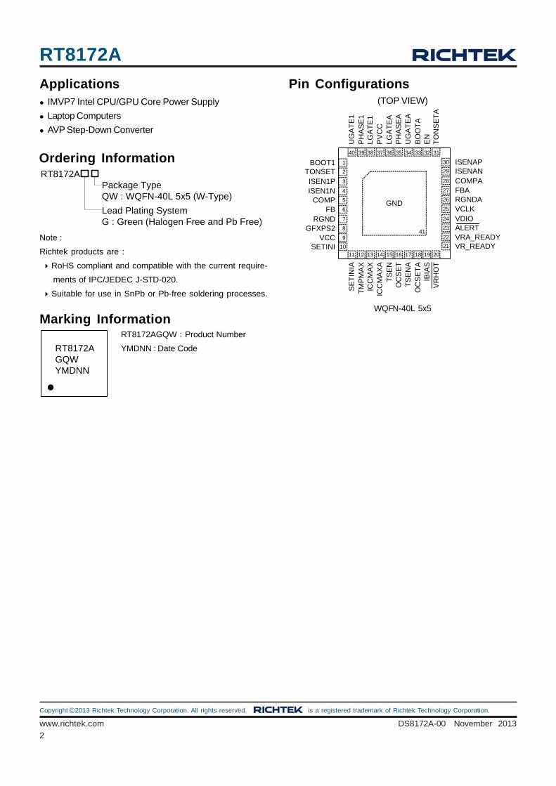
Pin Configurations(TOP VIEW)
WQFN-40L 5x5
Marking InformationRT8172AGQW : Product Number
YMDNN : Date Code
Package TypeQW : WQFN-40L 5x5 (W-Type)
RT8172A
Lead Plating SystemG : Green (Halogen Free and Pb Free)
RT8172AGQWYMDNN
BOOT1
ISEN1NISEN1P
SETINIVCC
GFXPS2RGND
COMPFB
TONSETISENAP
FBACOMPA
VR_READYVRA_READY
VDIO
RGNDAVCLK
ISENAN
SE
TIN
IAT
MP
MA
XIC
CM
AX
ICC
MA
XA
TS
EN
OC
SE
TT
SE
NA
OC
SE
TA
IBIA
S
UG
AT
E1
PH
AS
E1
LG
AT
E1
PV
CC
LG
AT
EA
PH
AS
EA
UG
AT
EA
BO
OT
AE
NT
ON
SE
TA
VR
HO
T
ALERT
1
2
3
4
5
6
7
8
9
10
30
29
28
27
26
25
24
23
22
21
20191817161514131211
31323334353637383940
41
GND
Applications IMVP7 Intel CPU/GPU Core Power Supply
Laptop Computers
AVP Step-Down Converter

RT8172A
3
DS8172A-00 November 2013 www.richtek.com
©Copyright 2013 Richtek Technology Corporation. All rights reserved. is a registered trademark of Richtek Technology Corporation.
VID7 VID6 VID5 VID4 VID3 VID2 VID1 VID0 H1 H0 VDAC Voltage
0 0 0 0 0 0 0 0 0 0 0.000
0 0 0 0 0 0 0 1 0 1 0.250
0 0 0 0 0 0 1 0 0 2 0.255
0 0 0 0 0 0 1 1 0 3 0.260
0 0 0 0 0 1 0 0 0 4 0.265
0 0 0 0 0 1 0 1 0 5 0.270
0 0 0 0 0 1 1 0 0 6 0.275
0 0 0 0 0 1 1 1 0 7 0.280
0 0 0 0 1 0 0 0 0 8 0.285
0 0 0 0 1 0 0 1 0 9 0.290
0 0 0 0 1 0 1 0 0 A 0.295
0 0 0 0 1 0 1 1 0 B 0.300
0 0 0 0 1 1 0 0 0 C 0.305
0 0 0 0 1 1 0 1 0 D 0.310
0 0 0 0 1 1 1 0 0 E 0.315
0 0 0 0 1 1 1 1 0 F 0.320
0 0 0 1 0 0 0 0 1 0 0.325
0 0 0 1 0 0 0 1 1 1 0.330
0 0 0 1 0 0 1 0 1 2 0.335
0 0 0 1 0 0 1 1 1 3 0.340
0 0 0 1 0 1 0 0 1 4 0.345
0 0 0 1 0 1 0 1 1 5 0.350
0 0 0 1 0 1 1 0 1 6 0.355
0 0 0 1 0 1 1 1 1 7 0.360
0 0 0 1 1 0 0 0 1 8 0.365
0 0 0 1 1 0 0 1 1 9 0.370
0 0 0 1 1 0 1 0 1 A 0.375
0 0 0 1 1 0 1 1 1 B 0.380
0 0 0 1 1 1 0 0 1 C 0.385
0 0 0 1 1 1 0 1 1 D 0.390
0 0 0 1 1 1 1 0 1 E 0.395
0 0 0 1 1 1 1 1 1 F 0.400
0 0 1 0 0 0 0 0 2 0 0.405
0 0 1 0 0 0 0 1 2 1 0.410
0 0 1 0 0 0 1 0 2 2 0.415
Table 1. IMVP7/VR12 Compliant VID Table

RT8172A
4
DS8172A-00 November 2013www.richtek.com
©Copyright 2013 Richtek Technology Corporation. All rights reserved. is a registered trademark of Richtek Technology Corporation.
VID7 VID6 VID5 VID4 VID3 VID2 VID1 VID0 H1 H0 DAC Voltage
0 0 1 0 0 0 1 1 2 3 0.420
0 0 1 0 0 1 0 0 2 4 0.425
0 0 1 0 0 1 0 1 2 5 0.430
0 0 1 0 0 1 1 0 2 6 0.435
0 0 1 0 0 1 1 1 2 7 0.440
0 0 1 0 1 0 0 0 2 8 0.445
0 0 1 0 1 0 0 1 2 9 0.450
0 0 1 0 1 0 1 0 2 A 0.455
0 0 1 0 1 0 1 1 2 B 0.460
0 0 1 0 1 1 0 0 2 C 0.465
0 0 1 0 1 1 0 1 2 D 0.470
0 0 1 0 1 1 1 0 2 E 0.475
0 0 1 0 1 1 1 1 2 F 0.480
0 0 1 1 0 0 0 0 3 0 0.485
0 0 1 1 0 0 0 1 3 1 0.490
0 0 1 1 0 0 1 0 3 2 0.495
0 0 1 1 0 0 1 1 3 3 0.500
0 0 1 1 0 1 0 0 3 4 0.505
0 0 1 1 0 1 0 1 3 5 0.510
0 0 1 1 0 1 1 0 3 6 0.515
0 0 1 1 0 1 1 1 3 7 0.520
0 0 1 1 1 0 0 0 3 8 0.525
0 0 1 1 1 0 0 1 3 9 0.530
0 0 1 1 1 0 1 0 3 A 0.535
0 0 1 1 1 0 1 1 3 B 0.540
0 0 1 1 1 1 0 0 3 C 0.545
0 0 1 1 1 1 0 1 3 D 0.550
0 0 1 1 1 1 1 0 3 E 0.555
0 0 1 1 1 1 1 1 3 F 0.560
0 1 0 0 0 0 0 0 4 0 0.565
0 1 0 0 0 0 0 1 4 1 0.570
0 1 0 0 0 0 1 0 4 2 0.575
0 1 0 0 0 0 1 1 4 3 0.580
0 1 0 0 0 1 0 0 4 4 0.585
0 1 0 0 0 1 0 1 4 5 0.590

RT8172A
5
DS8172A-00 November 2013 www.richtek.com
©Copyright 2013 Richtek Technology Corporation. All rights reserved. is a registered trademark of Richtek Technology Corporation.
VID7 VID6 VID5 VID4 VID3 VID2 VID1 VID0 H1 H0 DAC Voltage
0 1 0 0 0 1 1 0 4 6 0.595
0 1 0 0 0 1 1 1 4 7 0.600
0 1 0 0 1 0 0 0 4 8 0.605
0 1 0 0 1 0 0 1 4 9 0.610
0 1 0 0 1 0 1 0 4 A 0.615
0 1 0 0 1 0 1 1 4 B 0.620
0 1 0 0 1 1 0 0 4 C 0.625
0 1 0 0 1 1 0 1 4 D 0.630
0 1 0 0 1 1 1 0 4 E 0.635
0 1 0 0 1 1 1 1 4 F 0.640
0 1 0 1 0 0 0 0 5 0 0.645
0 1 0 1 0 0 0 1 5 1 0.650
0 1 0 1 0 0 1 0 5 2 0.655
0 1 0 1 0 0 1 1 5 3 0.660
0 1 0 1 0 1 0 0 5 4 0.665
0 1 0 1 0 1 0 1 5 5 0.670
0 1 0 1 0 1 1 0 5 6 0.675
0 1 0 1 0 1 1 1 5 7 0.680
0 1 0 1 1 0 0 0 5 8 0.685
0 1 0 1 1 0 0 1 5 9 0.690
0 1 0 1 1 0 1 0 5 A 0.695
0 1 0 1 1 0 1 1 5 B 0.700
0 1 0 1 1 1 0 0 5 C 0.705
0 1 0 1 1 1 0 1 5 D 0.710
0 1 0 1 1 1 1 0 5 E 0.715
0 1 0 1 1 1 1 1 5 F 0.720
0 1 1 0 0 0 0 0 6 0 0.725
0 1 1 0 0 0 0 1 6 1 0.730
0 1 1 0 0 0 1 0 6 2 0.735
0 1 1 0 0 0 1 1 6 3 0.740
0 1 1 0 0 1 0 0 6 4 0.745
0 1 1 0 0 1 0 1 6 5 0.750
0 1 1 0 0 1 1 0 6 6 0.755
0 1 1 0 0 1 1 1 6 7 0.760
0 1 1 0 1 0 0 0 6 8 0.765
0 1 1 0 1 0 0 1 6 9 0.770

RT8172A
6
DS8172A-00 November 2013www.richtek.com
©Copyright 2013 Richtek Technology Corporation. All rights reserved. is a registered trademark of Richtek Technology Corporation.
VID7 VID6 VID5 VID4 VID3 VID2 VID1 VID0 H1 H0 DAC Voltage
0 1 1 0 1 0 1 0 6 A 0.775
0 1 1 0 1 0 1 1 6 B 0.780
0 1 1 0 1 1 0 0 6 C 0.785
0 1 1 0 1 1 0 1 6 D 0.790
0 1 1 0 1 1 1 0 6 E 0.795
0 1 1 0 1 1 1 1 6 F 0.800
0 1 1 1 0 0 0 0 7 0 0.805
0 1 1 1 0 0 0 1 7 1 0.810
0 1 1 1 0 0 1 0 7 2 0.815
0 1 1 1 0 0 1 1 7 3 0.820
0 1 1 1 0 1 0 0 7 4 0.825
0 1 1 1 0 1 0 1 7 5 0.830
0 1 1 1 0 1 1 0 7 6 0.835
0 1 1 1 0 1 1 1 7 7 0.840
0 1 1 1 1 0 0 0 7 8 0.845
0 1 1 1 1 0 0 1 7 9 0.850
0 1 1 1 1 0 1 0 7 A 0.855
0 1 1 1 1 0 1 1 7 B 0.860
0 1 1 1 1 1 0 0 7 C 0.865
0 1 1 1 1 1 0 1 7 D 0.870
0 1 1 1 1 1 1 0 7 E 0.875
0 1 1 1 1 1 1 1 7 F 0.880
1 0 0 0 0 0 0 0 8 0 0.885
1 0 0 0 0 0 0 1 8 1 0.890
1 0 0 0 0 0 1 0 8 2 0.895
1 0 0 0 0 0 1 1 8 3 0.900
1 0 0 0 0 1 0 0 8 4 0.905
1 0 0 0 0 1 0 1 8 5 0.910
1 0 0 0 0 1 1 0 8 6 0.915
1 0 0 0 0 1 1 1 8 7 0.920
1 0 0 0 1 0 0 0 8 8 0.925
1 0 0 0 1 0 0 1 8 9 0.930
1 0 0 0 1 0 1 0 8 A 0.935
1 0 0 0 1 0 1 1 8 B 0.940
1 0 0 0 1 1 0 0 8 C 0.945
1 0 0 0 1 1 0 1 8 D 0.950

RT8172A
7
DS8172A-00 November 2013 www.richtek.com
©Copyright 2013 Richtek Technology Corporation. All rights reserved. is a registered trademark of Richtek Technology Corporation.
VID7 VID6 VID5 VID4 VID3 VID2 VID1 VID0 H1 H0 DAC Voltage
1 0 0 0 1 1 1 0 8 E 0.955
1 0 0 0 1 1 1 1 8 F 0.960
1 0 0 1 0 0 0 0 9 0 0.965
1 0 0 1 0 0 0 1 9 1 0.970
1 0 0 1 0 0 1 0 9 2 0.975
1 0 0 1 0 0 1 1 9 3 0.980
1 0 0 1 0 1 0 0 9 4 0.985
1 0 0 1 0 1 0 1 9 5 0.990
1 0 0 1 0 1 1 0 9 6 0.995
1 0 0 1 0 1 1 1 9 7 1.000
1 0 0 1 1 0 0 0 9 8 1.005
1 0 0 1 1 0 0 1 9 9 1.010
1 0 0 1 1 0 1 0 9 A 1.015
1 0 0 1 1 0 1 1 9 B 1.020
1 0 0 1 1 1 0 0 9 C 1.025
1 0 0 1 1 1 0 1 9 D 1.030
1 0 0 1 1 1 1 0 9 E 1.035
1 0 0 1 1 1 1 1 9 F 1.040
1 0 1 0 0 0 0 0 A 0 1.045
1 0 1 0 0 0 0 1 A 1 1.050
1 0 1 0 0 0 1 0 A 2 1.055
1 0 1 0 0 0 1 1 A 3 1.060
1 0 1 0 0 1 0 0 A 4 1.065
1 0 1 0 0 1 0 1 A 5 1.070
1 0 1 0 0 1 1 0 A 6 1.075
1 0 1 0 0 1 1 1 A 7 1.080
1 0 1 0 1 0 0 0 A 8 1.085
1 0 1 0 1 0 0 1 A 9 1.090
1 0 1 0 1 0 1 0 A A 1.095
1 0 1 0 1 0 1 1 A B 1.100
1 0 1 0 1 1 0 0 A C 1.105
1 0 1 0 1 1 0 1 A D 1.110
1 0 1 0 1 1 1 0 A E 1.115
1 0 1 0 1 1 1 1 A F 1.120
1 0 1 1 0 0 0 0 B 0 1.125
1 0 1 1 0 0 0 1 B 1 1.130

RT8172A
8
DS8172A-00 November 2013www.richtek.com
©Copyright 2013 Richtek Technology Corporation. All rights reserved. is a registered trademark of Richtek Technology Corporation.
VID7 VID6 VID5 VID4 VID3 VID2 VID1 VID0 H1 H0 DAC Voltage
1 0 1 1 0 0 1 0 B 2 1.135
1 0 1 1 0 0 1 1 B 3 1.140
1 0 1 1 0 1 0 0 B 4 1.145
1 0 1 1 0 1 0 1 B 5 1.150
1 0 1 1 0 1 1 0 B 6 1.155
1 0 1 1 0 1 1 1 B 7 1.160
1 0 1 1 1 0 0 0 B 8 1.165
1 0 1 1 1 0 0 1 B 9 1.170
1 0 1 1 1 0 1 0 B A 1.175
1 0 1 1 1 0 1 1 B B 1.180
1 0 1 1 1 1 0 0 B C 1.185
1 0 1 1 1 1 0 1 B D 1.190
1 0 1 1 1 1 1 0 B E 1.195
1 0 1 1 1 1 1 1 B F 1.200
1 1 0 0 0 0 0 0 C 0 1.205
1 1 0 0 0 0 0 1 C 1 1.210
1 1 0 0 0 0 1 0 C 2 1.215
1 1 0 0 0 0 1 1 C 3 1.220
1 1 0 0 0 1 0 0 C 4 1.225
1 1 0 0 0 1 0 1 C 5 1.230
1 1 0 0 0 1 1 0 C 6 1.235
1 1 0 0 0 1 1 1 C 7 1.240
1 1 0 0 1 0 0 0 C 8 1.245
1 1 0 0 1 0 0 1 C 9 1.250
1 1 0 0 1 0 1 0 C A 1.255
1 1 0 0 1 0 1 1 C B 1.260
1 1 0 0 1 1 0 0 C C 1.265
1 1 0 0 1 1 0 1 C D 1.270
1 1 0 0 1 1 1 0 C E 1.275
1 1 0 0 1 1 1 1 C F 1.280
1 1 0 1 0 0 0 0 D 0 1.285
1 1 0 1 0 0 0 1 D 1 1.290
1 1 0 1 0 0 1 0 D 2 1.295
1 1 0 1 0 0 1 1 D 3 1.300
1 1 0 1 0 1 0 0 D 4 1.305
1 1 0 1 0 1 0 1 D 5 1.310

RT8172A
9
DS8172A-00 November 2013 www.richtek.com
©Copyright 2013 Richtek Technology Corporation. All rights reserved. is a registered trademark of Richtek Technology Corporation.
VID7 VID6 VID5 VID4 VID3 VID2 VID1 VID0 H1 H0 DAC Voltage
1 1 0 1 0 1 1 0 D 6 1.315
1 1 0 1 0 1 1 1 D 7 1.320
1 1 0 1 1 0 0 0 D 8 1.325
1 1 0 1 1 0 0 1 D 9 1.330
1 1 0 1 1 0 1 0 D A 1.335
1 1 0 1 1 0 1 1 D B 1.340
1 1 0 1 1 1 0 0 D C 1.345
1 1 0 1 1 1 0 1 D D 1.350
1 1 0 1 1 1 1 0 D E 1.355
1 1 0 1 1 1 1 1 D F 1.360
1 1 1 0 0 0 0 0 E 0 1.365
1 1 1 0 0 0 0 1 E 1 1.370
1 1 1 0 0 0 1 0 E 2 1.375
1 1 1 0 0 0 1 1 E 3 1.380
1 1 1 0 0 1 0 0 E 4 1.385
1 1 1 0 0 1 0 1 E 5 1.390
1 1 1 0 0 1 1 0 E 6 1.395
1 1 1 0 0 1 1 1 E 7 1.400
1 1 1 0 1 0 0 0 E 8 1.405
1 1 1 0 1 0 0 1 E 9 1.410
1 1 1 0 1 0 1 0 E A 1.415
1 1 1 0 1 0 1 1 E B 1.420
1 1 1 0 1 1 0 0 E C 1.425
1 1 1 0 1 1 0 1 E D 1.430
1 1 1 0 1 1 1 0 E E 1.435
1 1 1 0 1 1 1 1 E F 1.440
1 1 1 1 0 0 0 0 F 0 1.445
1 1 1 1 0 0 0 1 F 1 1.450
1 1 1 1 0 0 1 0 F 2 1.455
1 1 1 1 0 0 1 1 F 3 1.460
1 1 1 1 0 1 0 0 F 4 1.465
1 1 1 1 0 1 0 1 F 5 1.470
1 1 1 1 0 1 1 0 F 6 1.475
1 1 1 1 0 1 1 1 F 7 1.480
1 1 1 1 1 0 0 0 F 8 1.485

RT8172A
10
DS8172A-00 November 2013www.richtek.com
©Copyright 2013 Richtek Technology Corporation. All rights reserved. is a registered trademark of Richtek Technology Corporation.
VID7 VID6 VID5 VID4 VID3 VID2 VID1 VID0 H1 H0 DAC Voltage
1 1 1 1 1 0 0 1 F 9 1.490
1 1 1 1 1 0 1 0 F A 1.495
1 1 1 1 1 0 1 1 F B 1.500
1 1 1 1 1 1 0 0 F C 1.505
1 1 1 1 1 1 0 1 F D 1.510
1 1 1 1 1 1 1 0 F E 1.515
1 1 1 1 1 1 1 1 F F 1.520

RT8172A
11
DS8172A-00 November 2013 www.richtek.com
©Copyright 2013 Richtek Technology Corporation. All rights reserved. is a registered trademark of Richtek Technology Corporation.
Functional Pin DescriptionPin No. Pin Name Pin Function
1 BOOT1 CPU VR Bootstrap Supply for High-Side Gate Driver. This pin powers the high-side MOSFET drivers. Connect this pin to the PHASE1 pin with a bootstrap capacitor.
2 TONSET Single-Phase CPU VR On-Time Setting Pin. Connect this pin to VIN with a resistor to set ripple size in PWM mode.
3 ISEN1P Positive Current Sense Input of CPU VR.
4 ISEN1N Negative Current Sense Input of CPU VR.
5 COMP CPU VR Compensation Node. This pin is the output of the error amplifier.
6 FB CPU VR Feedback Voltage Input. This pin is the inverting input node of the error amplifier.
7 RGND Return Ground for CPU VR. This pin is the inverting input node for differential remote voltage sensing.
8 GFXPS2 Set Pin for GPU VR Operation Mode. Logic-high on this pin will force the GPU VR to enter DCM.
9 VCC Controller Power Supply Input. Connect this pin to GND via a ceramic capacitor larger than 1F.
10 SETINI ADC Input for Single-Phase CPU VR VBOOT Voltage Setting.
11 SETINIA ADC Input for Single-Phase GPU VR VBOOT Voltage Setting.
12 TMPMAX ADC Input for Single-Phase CPU VR Maximum Temperature Setting.
13 ICCMAX ADC Input for Single-Phase CPU VR Maximum Current Setting.
14 ICCMAXA ADC Input for Single-Phase GPU VR Maximum Current Setting.
15 TSEN Thermal Monitor Sense Input Pin for CPU VR.
16 OCSET
Single-Phase CPU VR Over-Current Protection Threshold Setting. Connect a resistive voltage divider from VCC to ground, and connect the joint of the voltage divider to the OCSET pin. The voltage, VOCSET, at this pin sets the over current threshold, ILIMIT, for CPU VR.
17 TSENA Thermal Monitor Sense Input for GPU VR.
18 OCSETA
Single-Phase GPU VR Over-Current Protection Threshold Setting. Connect a resistive voltage divider from VCC to ground, and connect the joint of the voltage divider to the OCSETA pin. The voltage, VOCSETA, at this pin sets the over-current threshold, ILIMIT, for GPU VR.
19 IBIAS Internal Bias Current Setting. Connect a 53.6k resistor from this pin to GND to set the internal bias current.
20 VRHOT Thermal Monitor Output (Active-Low).
21 VR_READY CPU VR Voltage Ready Indicator. This pin has an open-drain output.
22 VRA_READY GPU VR Voltage Ready Indicator. This pin has an open-drain output.
23 ALERT Alert Line of SVID Interface (active low). This pin has an open drain output.
24 VDIO Data Transmission Line of SVID Interface.
25 VCLK Clock Signal Line of SVID Interface.
26 RGNDA Return Ground for Single-Phase GPU VR. This pin is the inverting input node for differential remote voltage sensing.

RT8172A
12
DS8172A-00 November 2013www.richtek.com
©Copyright 2013 Richtek Technology Corporation. All rights reserved. is a registered trademark of Richtek Technology Corporation.
Pin No. Pin Name Pin Function
27 FBA GPU VR Feedback Voltage Input. This pin is the inverting input node of the error amplifier.
28 COMPA Single-Phase GPU VR Compensation Node. This pin is the output of the error amplifier.
29 ISENAN Negative Current Sense Input of Single-Phase GPU VR.
30 ISENAP Positive Current Sense Input of Single-Phase GPU VR.
31 TONSETA Single-Phase GPU VR On-Time Setting. Connect this pin to VIN with a resistor to set ripple size in PWM mode.
32 EN Voltage Regulator Enable Signal Input Pin.
33 BOOTA GPU VR Bootstrap Supply for High-Side Gate Driver. This pin powers the high-side MOSFET drivers. Connect this pin to the PHASEA pin with a bootstrap capacitor.
34 UGATEA High-Side Gate Driver of GPU VR. This pin drives the high-side MOSFET of GPU VR.
35 PHASEA Switch Node of GPU VR. This pin is the return node of the high-side MOSFET driver for GPU VR. Connect this pin to the joint of the Source of high-side MOSFET, Drain of the low-side MOSFET, and the output inductor.
36 LGATEA Low-Side Gate Driver of GPU VR. This pin drives the low side MOSFET of GPU VR.
37 PVCC MOSFET Driver Power Supply Pin. Connect this pin to GND via a ceramic capacitor larger than 1F.
38 LGATE1 Low-Side Gate Driver of CPU VR. This pin drives the low-side MOSFET of CPU VR.
39 PHASE1 Switch Node of CPU VR. This pin is the return node of the high-side driver for CPU VR. Connect this pin to the joint of the Source of high-side MOSFET, Drain of the low-side MOSFET, and the output inductor.
40 UGATE1 High-Side Gate Driver of CPU VR. This pin drives the high-side MOSFET of CPU VR.
41 (Exposed Pad) GND Ground of Low-Side MOSFET Driver. The exposed pad must be soldered to a large PCB and connected to GND for maximum power dissipation.

RT8172A
13
DS8172A-00 November 2013 www.richtek.com
©Copyright 2013 Richtek Technology Corporation. All rights reserved. is a registered trademark of Richtek Technology Corporation.
Function Block Diagram
ICC
MA
X
ICC
MA
XA
TS
EN
FBA
COMPA
ERROR AMP
TM
PM
AX
Control & Protection Logic
MUX
ADCSVID XCVR
VD
IO
VC
LK
EN
VR
_RE
AD
Y
VR
A_R
EA
DY
RGNDA
PWM CMP
From Control Logic
VREFA
VC
C
UVLO
PVCC
BOOTA
UGATEA
PHASEA
LGATEA
SE
TIN
IA
SE
TIN
I
TS
EN
A
TONSETATON Time Generator
Driver Logic Control
Offset Cancellation
GFXPS2
VR
HO
T
+
-
+
-
ALE
RT
DAC
+
-10OCPOVP/UVP/NVP
ERROR AMP
RGND
PWM CMP
From Control Logic
Soft-Start & Slew Rate Control
VREF
BOOT1
UGATE1
PHASE1
LGATE1
TONSETTON Time Generator
Driver Logic Control
Offset Cancellation
+
-
+
-
DAC
To Protection Logic
Soft-Start & Slew Rate Control
+
-10 OCP OVP/UVP/NVP
To Protection Logic
FB
COMP
ISEN1P
ISEN1N
OCSET
ISENAP
ISENAN
OCSETA
IBIAS

RT8172A
14
DS8172A-00 November 2013www.richtek.com
©Copyright 2013 Richtek Technology Corporation. All rights reserved. is a registered trademark of Richtek Technology Corporation.
Operation
The RT8172A adopts the G-NAVPTM (Green Native AVP)
which is Richtek's proprietary topology derived from finite
DC gain of EA amplifier with current mode control, making
it easy to set the droop to meet all Intel CPU requirements
of AVP (Adaptive Voltage Positioning).
The RT8172A adopts the G-NAVPTM controller, which is
one type of current mode constant on-time control with
DC offset cancellation. The approach not only can improve
DC offset problem for increasing system accuracy but also
can have fast transient response for saving BOM. For the
RT8172A, when current feedback signal reaches comp
signal to generate an on-time width to achieve PWM
modulation.
TON GEN
Generate the UGATEx pulse according to the phase control
signal from the loop control protection logic.
SVID XCVR Interface
The interface that receive the SVID signal from CPU
and sent the relative signals to Loop Control Protection
logic to execute the action by CPU.
The SVID logic that control the ADC timing.
Control & Protection Logic
The registers that save the pin setting data from ADC
output
The control logic also generate the digital code of the
VID that relative to VSET.
Control the on phase of PWM and the on time interval
of PWM according to PWMCMP output.
Control the power on sequence.
Control the protection behavior.
Control the operational phase number.
Offset Cancellation
Cancel the current/voltage ripple issue to get the accurate
VSEN.
UVLO
Detect the VCC voltage and issue POR signal as VCC is
high enough.
DAC
Generate a analog signal according the digital code
generated by Control Logic.
Soft-Start & Slew Rate Control
Control the Dynamic VID slew rate of VSET according to
the SetVID fast or SetVID slow.

RT8172A
15
DS8172A-00 November 2013 www.richtek.com
©Copyright 2013 Richtek Technology Corporation. All rights reserved. is a registered trademark of Richtek Technology Corporation.
Recommended Operating Conditions (Note 4)
Supply Voltage, VCC ------------------------------------------------------------------------------------- 4.5V to 5.5V
Input Voltage, VIN ----------------------------------------------------------------------------------------- 5V to 25V
Junction Temperature Range--------------------------------------------------------------------------- −40°C to 125°C Ambient Temperature Range--------------------------------------------------------------------------- −40°C to 85°C
Absolute Maximum Ratings (Note 1)
PVCC, VCC to GND ------------------------------------------------------------------------------------- −0.3V to 6.5V
RGNDx to GND ------------------------------------------------------------------------------------------- −0.3V to 0.3V
TONSETx to GND ---------------------------------------------------------------------------------------- −0.3V to 28V
Other Pins-------------------------------------------------------------------------------------------------- −0.3V to (VCC + 0.3V)
BOOTx to PHASEx -------------------------------------------------------------------------------------- −0.3V to 6.5V
PHASEx to GND
DC------------------------------------------------------------------------------------------------------------ −3V to 28V
<20ns ------------------------------------------------------------------------------------------------------- −8V to 32V
UGATEx to PHASEx
DC------------------------------------------------------------------------------------------------------------ −0.3V to (BOOTx − PHASEx)
<20ns ------------------------------------------------------------------------------------------------------- −5V to 7.5V
LGATEx to GND
DC------------------------------------------------------------------------------------------------------------ −0.3V to (PVCC + 0.3V)
<20ns ------------------------------------------------------------------------------------------------------- −2.5V to 7.5V
Power Dissipation, PD @ TA = 25°C
WQFN−40L 5x5 ------------------------------------------------------------------------------------------- 3.63W
Package Thermal Resistance (Note 2)
WQFN−40L 5x5, θJA ------------------------------------------------------------------------------------- 27.5°C/W
WQFN−40L 5x5, θJC ------------------------------------------------------------------------------------- 6°C/W
Junction Temperature ------------------------------------------------------------------------------------ 150°C Lead Temperature (Soldering, 10 sec.) -------------------------------------------------------------- 260°C Storage Temperature Range --------------------------------------------------------------------------- −65°C to 150°C ESD Susceptibility (Note 3)
HBM (Human Body Model) ----------------------------------------------------------------------------- 2kV
MM (Machine Model) ------------------------------------------------------------------------------------ 200V
Electrical Characteristics(VCC = 5V, TA
= 25°C, unless otherwise specified)
Parameter Symbol Test Conditions Min Typ Max Unit
Supply Input
VCC/VPVCC VEN = 1.05V, Not Switching 4.5 5 5.5 Input Voltage Range
VIN Battery Input Voltage 5 -- 25 V
Supply Current (VCC + PVCC)
IVCC + IPVCC VEN = 1.05V, Not Switching -- 12 20 mA
Supply Current (TONSETx)
ITONSETx VFB =1V, VIN = 12V, RTON = 100k -- 110 -- A

RT8172A
16
DS8172A-00 November 2013www.richtek.com
©Copyright 2013 Richtek Technology Corporation. All rights reserved. is a registered trademark of Richtek Technology Corporation.
Parameter Symbol Test Conditions Min Typ Max Unit
Shutdown Current (PVCC + VCC)
IVCC_SHDN + IPVCC_SHDN
VEN = 0V -- -- 5 A
Shutdown Current (TONSETx)
ITONSETx_SHDN VEN = 0V -- -- 5 A
TON Setting
TONSETx Voltage VTONSETx IRTON = 80A, VFBx = 1V 0.95 1.075 1.2 V
On-Time tON IRTON = 80A, VFBx = 1V 315 350 385 ns
TONSETx Input Current Range
IRTON VFBx = 1.1V 25 -- 280 A
Minimum Off-Time TOFF_MIN -- 350 -- ns
GFX VR Forced DEM
GFXPS2x Enable Threshold
VGFXPS 4.3 -- -- V
GFXPS2x Disable Threshold
VGFXPS -- -- 0.7 V
References and System Output Voltage
VIDSVID Setting = 1.000V to 1.520V OFSSVID Setting = 0V
0.5 0 0.5 %VID
VIDSVID Setting = 0.800V to 1.000V OFSSVID Setting = 0V
5 0 5
VIDSVID Setting = 0.500V to 0.800V OFSSVID Setting = 0V
8 0 8
VIDSVID Setting = 0.250V to 0.500V OFSSVID Setting = 0V
8 0 8
DAC Accuracy (PS0/PS1)
VFBx
VIDSVID Setting = 1.100V OFSSVID Setting = 0.640V to 0.635V
10 0 10
mV
VINI_CORE = 0V, VINI_GFX = 0V 0 0.3125 0.5125
VINI_CORE = 0.9V, VINI_GFX = 0.9V 0.7375 0.9375 1.1375
VINI_CORE = 1V, VINI_GFX = 1V 1.3625 1.5625 1.7625 SETINIx Voltage VSETINIx
VINI_CORE = 1.1V, VINI_GFX = 1.1V 2.6125 -- 5
V
IBIAS Pin Voltage VIBIAS RIBIAS = 53.6k 2.09 2.14 2.19 V
SetVID Slow 2.5 3.125 3.75 Dynamic VID Slew Rate SRDVID
SetVID Fast 10 12.5 15 mV/s
Error Amplifier
DC Gain ADC RL = 47k (Note5) 70 80 -- dB
Gain-Bandwidth Product GBW CLOAD = 5pF (Note5) -- 10 -- MHz
Slew Rate SRCOMP CLOAD = 10pF (Gain = 4, RLOAD_COMP = 47k, VCOMPx = 0.5V to 3V)
-- 5 -- V/s
Output Voltage Range VCOMP RL = 47k 0.5 -- 3.6 V
MAX Source/Sink Current
ICOMP VCOMP = 2V -- 250 -- A
Impedance of FBx RFBx 1 -- -- M

RT8172A
17
DS8172A-00 November 2013 www.richtek.com
©Copyright 2013 Richtek Technology Corporation. All rights reserved. is a registered trademark of Richtek Technology Corporation.
Parameter Symbol Test Conditions Min Typ Max Unit
Current Sense Amplifier
Input Offset Voltage VOFS_CSA 1 -- 1 mV
Impedance of Neg. Input RISENxN 1 -- -- M
Impedance of Pos. Input RISENxP 1 -- -- M
Current Sense Differential Input Range
VCSDIx VFBx = 1.1V, VCSDIx = VISENxP VISENxN 50 -- 100 mV
Current Sense DC Gain (Loop)
AI VFBx = 1.1V, 30mV < VCSDIx < 50mV -- 10 -- V/V
VISEN Linearity VISEN_ACC VDAC = 1.1V 30mV < VISEN_IN < 50mV 1 -- 1 %
Gate Driver
High-Side Driver Source RUGATEx_sr VBOOTx VPHASEx = 5V VBOOTx VUGATEx = 0.1V
-- 1 --
High-Side Driver Sink RUGATEx_sk VUGATEx = 0.1V -- 1 --
Low-Side Driver Source RLGATEx_sr PVCC = 5V, PVCC VLGATEx = 0.1V -- 1 --
Low-Side Driver Sink RLGATEx_sk VLGATEx = 0.1V -- 0.5 --
Internal Boot Charging Switch On-Resistance
RBOOTx PVCC to BOOTx -- 30 --
Zero Current Detection Threshold
VZCD_TH VZCD_TH = GND VPHASEx -- 10 -- mV
Protection
Under-Voltage Lockout Threshold
VUVLO VCC Falling edge 4.04 4.24 -- V
Under-Voltage Lockout Hysteresis
VUVLO -- 100 -- mV
Over-Voltage Protection Threshold
VOVP Respect to VOUT_MAXSVID, with 1s filter time
100 150 200 mV
Under-Voltage Protection Threshold
VUVP VUVP = VISENxN VREFx, 0.8V < VREFx <1.52V, with 3s filter time
350 300 250 mV
Negative-Voltage Protection Threshold
VNVP VNVP = VISENxN GND 100 50 -- mV
Current Sense Gain for Over-Current Protection
AOC VOCSET = 2.4V, VISENxP VISENxN = 50mV
-- 48 -- V/V
Logic Inputs
EN Input Voltage
Logic-High VIH With respect to 1V, 70% 0.7 -- -- V
Logic-Low VIL With respect to 1V, 30% -- -- 0.3
Leakage Current of EN 1 -- 1 A
VCLK,VDIO Input Threshold Voltage
VIH With respect to Intel Spec. 0.65 -- -- V
VIL With respect to Intel Spec. -- -- 0.45
Leakage Current of VCLK, VDIO
ILEAK_IN 1 -- 1 A

RT8172A
18
DS8172A-00 November 2013www.richtek.com
©Copyright 2013 Richtek Technology Corporation. All rights reserved. is a registered trademark of Richtek Technology Corporation.
Parameter Symbol Test Conditions Min Typ Max Unit
ALERT
ALERT Low Voltage VALERT IALERT_ SINK = 4mA -- -- 0.4 V
VR Ready
VRx_READY Low Voltage VVRx_READY IVRx_READY_ SINK = 4mA -- -- 0.4 V
VRx_READY Delay tVRx_READY VISENxN = VBOOT to VVRx_READY high 70 100 160 s
Thermal Throttling
VRHOT Output Voltage VVRHOT IVRHOT_SINK = 40mA -- 0.4 -- V
High Impedance Output
ALERT, VRx_READY, VRHOT
ILEAK_OUT 1 -- 1 A
Temperature Zone
TSEN Threshold for Tmp_Zone [7] transition
VTSENx
100°C -- 1.8725 -- V
TSEN Threshold for Tmp_Zone [6] transition
97°C -- 1.8175 -- V
TSEN Threshold for Tmp_Zone [5] transition
94°C -- 1.7625 -- V
TSEN Threshold for Tmp_Zone [4] transition
91°C -- 1.7075 -- V
TSEN Threshold for Tmp_Zone [3] transition
88°C -- 1.6525 -- V
TSEN Threshold for Tmp_Zone [2] transition
VTSENx
85°C -- 1.5975 -- V
TSEN Threshold for Tmp_Zone [1] transition
82°C -- 1.5425 -- V
TSEN Threshold for Tmp_Zone [0] transition
75°C -- 1.4875 -- V
Update Period tTSEN -- 1600 -- s
ADC
Latency tLAT -- -- 400 s
Digital Code of ICCMAX
CICCMAX1 VICCMAX = 0.637V 29 32 35 decimal
CICCMAX2 VICCMAX = 1.2642V 61 64 67 decimal
CICCMAX3 VICCMAX = 2.5186V 125 128 131 decimal
Digital Code of ICCMAXA
CICCMAXA1 VICCMAXA = 0.1666V 5 8 11 decimal
CICCMAXA2 VICCMAXA = 0.3234V 13 16 19 decimal
CICCMAXA3 VICCMAXA = 0.637V 29 32 35 decimal
Digital Code of TMPMAX
CTMPMAX1 VTMPMAX = 1.6758V 82 85 88 decimal
CTMPMAX2 VTMPMAX = 1.9698V 97 100 103 decimal
CTMPMAX3 VTMPMAX = 2.4598V 122 125 128 decimal

RT8172A
19
DS8172A-00 November 2013 www.richtek.com
©Copyright 2013 Richtek Technology Corporation. All rights reserved. is a registered trademark of Richtek Technology Corporation.
Note 1. Stresses beyond those listed “Absolute Maximum Ratings” may cause permanent damage to the device. These are
stress ratings only, and functional operation of the device at these or any other conditions beyond those indicated in
the operational sections of the specifications is not implied. Exposure to absolute maximum rating conditions may
affect device reliability.
Note 2. θJA is measured at TA = 25°C on a high effective thermal conductivity four-layer test board per JEDEC 51-7. θJC is
measured at the exposed pad of the package.
Note 3. Devices are ESD sensitive. Handling precaution is recommended.
Note 4. The device is not guaranteed to function outside its operating conditions.
Note 5. Guaranteed by design.

RT8172A
20
DS8172A-00 November 2013www.richtek.com
©Copyright 2013 Richtek Technology Corporation. All rights reserved. is a registered trademark of Richtek Technology Corporation.
Typical Application Circuit
VCORE
40
39
38
32
2
ISEN1N
RT8172A
EN
TONSET
1
VCC
ISEN1P3
L1
VIN
C3
R14 C6C5
C1
C4
Q1
R5
R4
R13
C7
9
GND41 (Exposed Pad)
R2
COMP
FB
R21
C11C10CORE VCC SENSE
R23
C9
PVCCC8
37
R1
5V
6
5
4
RGND 7
C2
R3
Q2R12
NTC1R15
R28
34
35
36
31
ISENAN
TONSETA
ISENAP 30
L2
VIN
C14
R43C16 C17
R35
5V to 25V
R42
C15
R33
COMPA
FBA
R48
C20C19
R50
C1827
28
29
RGNDA 26
C12
R34
Q4R41
NTCAR44
R51
25 VCLKVCLK24 VDIOVDIO23ALERT
R8R7R6VCCP
22 VRA_READYVRA_READY21 VR_READYVR_READY
R9 R10 R11
VRHOT20
18 OCSETA
R17
VCC
1610 SETINI
R18 R19 R20
SETINIA11
R25 R26 R27R24
OCSETOCSETA
SETINISETINIA
OCSET
8 GFXPS2
VCC
12
13 ICCMAX
R29 R30 R31
ICCMAXA14
R37 R38 R39
TMPMAX
ICCMAX
TMPMAX
IBIAS19
R54
R47NTCT1R46
TSENA
TSEN15
17
NTCTA
VCC
R16
R22
R45
R52 R53
R49
5V
VCC
BOOT1
VGFX
VGFX
R32
R40
ALERT
VRHOT
UGATEA
PHASEA
LGATEA
5V to 25V
UGATE1
PHASE1
LGATE1
GFX VCC SENSE
GFX VSS SENSE
33 C13
Q3
BOOTAR36
CORE VSS SENSE
VCORE
GFXPS2
ICCMAXA
2.2
1µF
130 130 150 10k10k 75
27k 8.7k 10k 10k
10k10k NC NC
51k 150k 100k NC
33k 5.1k 1.6k 10k
12k 10kß = 3380
12k10kß = 3380
R71750
R72750
1k 1k53.6k
130k
0.1µF
5.1
10µF0
00.1µF 1µH
DCR = 7.6m
Optional
3.9k 0.068µF
2.4k4.7k 4.7k
ß = 3500
330µF/9m
C26330µF/9m
Optional Optional
71k 10k 100
100
Optional
0
1µF
130k 5.1
0.1µF
10µF0
0
0.1µF
0
Optional
11k 0.1µF
1.2k1k 1k
ß = 3650
330µF/15m
C27330µF/15m
OptionalOptional Optional
42k 10k 100
100
2µH
DCR = 14.6m
Enable
R55 C21
Optional
R56 C22
Optional

RT8172A
21
DS8172A-00 November 2013 www.richtek.com
©Copyright 2013 Richtek Technology Corporation. All rights reserved. is a registered trademark of Richtek Technology Corporation.
Typical Operating Characteristics
Boot VID = 1V
Time (100μs/Div)
CORE VR Power On from EN
EN(2V/Div)
VCORE
(500mV/Div)
VR_READY(2V/Div)
UGATE(20V/Div)
Time (100μs/Div)
CORE VR Power Off from EN
Boot VID = 1V
EN(2V/Div)
VCORE
(500mV/Div)
VR_READY(2V/Div)
UGATE(20V/Div)
VID = 1.1V
Time (100μs/Div)
CORE VR OCP
ILOAD
(10A/Div)
VCORE
(1V/Div)
VR_READY(1V/Div)
UGATE(20V/Div)
Time (40μs/Div)
CORE VR OVP and NVP
VID = 1.1V
LGATE(10V/Div)
VCORE
(1V/Div)
VR_READY(1V/Div)
UGATE(20V/Div)
0.7V to 1.2V, Slew Rate = Slow, ILOAD = 4A
Time (40μs/Div)
CORE VR Dynamic VID Up
VDIO(2V/Div)
VCLK(2V/Div)
VCORE
(500mV/Div)
ALERT(2V/Div)
Time (40μs/Div)
CORE VR Dynamic VID Down
1.2V to 0.7V, Slew Rate = Slow, ILOAD = 4A
ALERT(2V/Div)
VCORE
(500mV/Div)
VDIO(2V/Div)
VCLK(2V/Div)

RT8172A
22
DS8172A-00 November 2013www.richtek.com
©Copyright 2013 Richtek Technology Corporation. All rights reserved. is a registered trademark of Richtek Technology Corporation.
Time (10μs/Div)
CORE VR Dynamic VID Up
0.7V to 1.2V, Slew Rate = Fast, ILOAD = 4A
VDIO(2V/Div)
VCLK(2V/Div)
VCORE
(500mV/Div)
ALERT(2V/Div)
Time (10μs/Div)
CORE VR Dynamic VID Down
1.2V to 0.7V, Slew Rate = Fast, ILOAD = 4A
VCORE
(500mV/Div)
ALERT(2V/Div)
VDIO(2V/Div)
VCLK(2V/Div)
VID = 1.1V, ILOAD = 1A to 8A, Slew Time = 150ns
Time (100μs/Div)
CORE VR Load Transient
VCORE
(20mV/Div)
8
1
ILOAD
(A/Div)
Time (100μs/Div)
CORE VR Load Transient
VID = 1.1V, ILOAD = 8A to 1A, Slew Time = 150ns
VCORE
(20mV/Div)
8
1
ILOAD
(A/Div)
VID = 1.1V, PS0 to PS2, ILOAD = 0.2A
Time (100μs/Div)
CORE VR Mode Transition
UGATE(20V/Div)
VCLK(1V/Div)LGATE
(10V/Div)
VCORE
(20mV/Div)
Time (100μs/Div)
CORE VR Mode Transition
VID = 1.1V, PS2 to PS0, ILOAD = 0.2A
UGATE(20V/Div)
VCORE
(20mV/Div)
VCLK(1V/Div)LGATE
(10V/Div)

RT8172A
23
DS8172A-00 November 2013 www.richtek.com
©Copyright 2013 Richtek Technology Corporation. All rights reserved. is a registered trademark of Richtek Technology Corporation.
CORE VR VREF vs. Temperature
0.990
0.992
0.994
0.996
0.998
1.000
1.002
1.004
1.006
-50 -25 0 25 50 75 100 125
Temperature (°C)
VR
EF (
V)
Time (100μs/Div)
GFX VR OCP
ILOAD
(5A/Div)
VGFX
(1V/Div)
VRA_READY(1V/Div)UGATEA(20V/Div)
Time (40μs/Div)
GFX VR OVP and NVP
VID = 1.1V
LGATEA(10V/Div)
VGFX
(1V/Div)
VRA_READY(1V/Div)
UGATEA(20V/Div)
Time (100μs/Div)
GFX VR Power On from EN
Boot VID = 1V
EN(2V/Div)
VGFX
(500mV/Div)
VRA_READY(2V/Div)
UGATEA(20V/Div)
Time (100μs/Div)
GFX VR Power Off from EN
Boot VID = 1V
UGATEA(20V/Div)
EN(2V/Div)
VGFX
(500mV/Div)
VRA_READY(2V/Div)
TSEN Sweep from 1.7V to 1.9V
Time (10ms/Div)
CORE VR Thermal Monitoring
VRHOT(500mV/Div)
TSEN(V/Div)
1.9
1.7

RT8172A
24
DS8172A-00 November 2013www.richtek.com
©Copyright 2013 Richtek Technology Corporation. All rights reserved. is a registered trademark of Richtek Technology Corporation.
Time (40μs/Div)
GFX VR Dynamic VID
0.7V to 1.2V, Slew Rate = Slow, ILOAD = 1.25A
VDIO(2V/Div)
VCLK(2V/Div)
VGFX
(500mV/Div)
ALERT(2V/Div)
Time (40μs/Div)
GFX VR Dynamic VID
ALERT(2V/Div)
VGFX
(500mV/Div)
1.2V to 0.7V, Slew Rate = Slow, ILOAD = 1.25A
VDIO(2V/Div)
VCLK(2V/Div)
Time (10μs/Div)
GFX VR Dynamic VID
0.7V to 1.2V, Slew Rate = Fast, ILOAD = 1.25A
VDIO(2V/Div)
VCLK(2V/Div)
VGFX
(500mV/Div)
ALERT(2V/Div)
Time (10μs/Div)
GFX VR Dynamic VID
ALERT(2V/Div) 1.2V to 0.7V, Slew Rate = Fast, ILOAD = 1.25A
VDIO(2V/Div)
VCLK(2V/Div)
VGFX
(500mV/Div)
Time (100μs/Div)
GFX VR Load Transient
VID = 1.1V, ILOAD = 1A to 4A, Slew Time = 150ns
VGFX
(20mV/Div)
4
1
ILOAD
(A/Div)
Time (100μs/Div)
GFX VR Load Transient
VID = 1.1V, ILOAD = 4A to 1A, Slew Time = 150ns
VGFX
(20mV/Div)
4
1
ILOAD
(A/Div)

RT8172A
25
DS8172A-00 November 2013 www.richtek.com
©Copyright 2013 Richtek Technology Corporation. All rights reserved. is a registered trademark of Richtek Technology Corporation.
GFX VR VREF vs. Temperature
0.988
0.990
0.992
0.994
0.996
0.998
1.000
1.002
1.004
1.006
-50 -25 0 25 50 75 100 125
Temperature (°C)
VR
EF (
V)
Time (100μs/Div)
GFX VR Mode Transition
VID = 1.1V, PS2 to PS0, ILOAD = 0.1A
UGATEA(20V/Div)
VGFX
(20mV/Div)
VCLK(1V/Div)
LGATEA(10V/Div)
Time (100μs/Div)
GFX VR Mode Transition
VID = 1.1V, PS0 to PS2, ILOAD = 0.1A
UGATEA(20V/Div)
VCLK(1V/Div)
LGATEA(10V/Div)
VGFX
(20mV/Div)
Time (10ms/Div)
GFX VR Thermal Monitoring
TSENA Sweep from 1.7V to 1.9V
1.9
1.7
TSENA(V/Div)
VRHOT(500mV/Div)

RT8172A
26
DS8172A-00 November 2013www.richtek.com
©Copyright 2013 Richtek Technology Corporation. All rights reserved. is a registered trademark of Richtek Technology Corporation.
Application Information
The RT8172A is a VR12/IMVP7 compliant, dual single-
phase synchronous Buck PWM controller for the CPU
CORE VR and GFX VR. The gate drivers are embedded
to facilitate PCB design and reduce the total BOM cost. A
serial VID (SVID) interface is built-in in the RT8172A to
communicate with Intel VR12/IMVP7 compliant CPU.
The RT8172A adopts G-NAVPTM (Green Native AVP), which
is Richtek's proprietary topology derived from finite DC
gain compensator, making it an easy setting PWM
controller to meet AVP requirements. The load-line can
be easily programmed by setting the DC gain of the error
amplifier. The RT8172A has fast transient response due to
the G-NAVPTM commanding variable switching frequency.
The G-NAVPTM topology also represents a high efficiency
system with green power concept. With the G-NAVPTM
topology, the RT8172A becomes a green power controller
with high efficiency under heavy load, light load, and very
light load conditions. The RT8172A supports mode
transition function between CCM and DEM. These different
operating states allow the overall power system to have
low power loss. By utilizing the G-NAVPTM topology, the
operating frequency of RT8172A varies with output voltage,
load and VIN to further enhance the efficiency even in CCM.
The built-in high accuracy DAC converts the SVID code
ranging from 0.25V to 1.52V with 5mV per step. The
differential remote output voltage sense and high accuracy
DAC allow the system to have high output voltage accuracy.
The RT8172A supports VR12/IMVP7 compatible power
management states and VID on-the-fly function. The power
management states include DEM in PS2/PS3 and Forced-
CCM in PS1/PS0. The VID on-the-fly function has three
different slew rates : Fast, Slow and Decay. The RT8172A
integrates a high accuracy ADC for platform setting
functions, such as no-load offset and over current level.
The controller supports both DCR and sense-resistor
current sensing. The RT8172A provides VR ready output
signals of both CORE VR and GFX VR. It also features
complete fault protection functions including over voltage,
under-voltage, negative-voltage, over-current and under-
voltage lockout. The RT8172A is available in the WQFN-
40L 5x5 small foot print package.
Design Tool
To help users reduce efforts and errors caused by manual
calculations, a user-friendly design tool is now available
on request. This design tool calculates all necessary
design parameters by entering user's requirements.
Please contact Richtek's representatives for details.
Serial VID (SVID) Interface
SVID is a three-wire serial synchronous interface defined
by Intel. The three wire bus includes VDIO, VCLK and
ALERT signals. The master (Intel's VR12/IMVP7 CPU)
initiates and terminates SVID transactions and drives the
VDIO, VCLK, and ALERT during a transaction. The slave
(RT8172A) receives the SVID transactions and acts
accordingly.

RT8172A
27
DS8172A-00 November 2013 www.richtek.com
©Copyright 2013 Richtek Technology Corporation. All rights reserved. is a registered trademark of Richtek Technology Corporation.
Standard Serial VID Command
Code Commands Master Payload
Contents Slave Payload
Contents Description
00h not supported N/A N/A N/A
01h SetVID_Fast VID code N/A Set new target VID code, VR jumps to new VID target with controlled default “fast” slew rate 12.5mV/s.
02h SetVID_Slow VID code N/A Set new target VID code, VR jumps to new VID target with controlled default “slow” slew rate 3.125mV/s.
03h SetVID_Decay VID code N/A
Set new target VID code, VR jumps to new VID target, but does not control the slew rate. The output voltage decays at a rate proportional to the load current
04h SetPS Byte indicating power states
N/A Set power state
05h SetRegADR Pointer of registers
in data table N/A Set the pointer of the data register
06h SetReg DAT New data register
content N/A Write the contents to the data register
07h GetReg Pointer of registers
in data table
Specified Register Contents
Slave returns the contents of the specified register as the payload
08h -
1Fh not supported N/A N/A N/A

RT8172A
28
DS8172A-00 November 2013www.richtek.com
©Copyright 2013 Richtek Technology Corporation. All rights reserved. is a registered trademark of Richtek Technology Corporation.
Data and Configuration Register
Index Register Name Description Access Default
00h Vendor ID Vendor ID, default 1Eh. RO, Vendor 1Eh
01h Product ID Product ID. RO, Vendor 65h
02h Product Revision Product Revision. RO, Vendor 01h
05h Protocol ID SVID Protocol ID. RO, Vendor 01h
06h VR_Capability Bit mapped register, identifies the SVID VR capabilities and which of the optional telemetry register are supported.
RO, Vendor 81h
10h Status_1 Data register containing the status of VR. R-M, W-PWM 00h
11h Status-2 Data register containing the status of transmission. R-M, W-PWM 00h
12h Temperature Zone
Data register showing temperature zone that have been entered.
R-M, W-PWM 00h
15h Output_Current Data register showing direct ADC conversion of averaged output current.
R-M, W-PWM 00h
1Ch Status_2_lastread The register contains a copy of the status_2. R-M, W-PWM 00h
21h ICC_Max Data register containing the maximum ICC of platform supports. Binary format in Amp, IE 64h = 100A.
RO, Platform --
22h Temp_Max
Data register containing the temperature max the platform supports. Binary format in °C, IE 64h = 100°C Only for CORE VR
RO, Platform --
24h SR-Fast Data register containing the capability of fast slew rate the platform can sustains. Binary format in mV/s, IE 0Ah = 10mV/s.
RO 0Ah
25h SR-Slow Data register containing the capability of slow slew rate. Binary format in mV/s IE 02h = 2.5mV/s.
RO 02h
30h VOUT_Max The register is programmed by the master and sets the maximum VID.
RW, Master FBh
31h VID Setting Data register containing currently programmed VID. RW, Master 00h
32h Power State Register containing the current programmed power state. RW, Master 00h
33h Offset Set offset in VID steps. RW, Master 00h
34h Multi VR Config Bit mapped data register which configures multiple VRs behavior on the same bus.
RW, Master 00h
35h Pointer Scratch pad register for temporary storage of the SetRegADR pointer register.
RW, Master 30h
Notes :
RO = Read Only
RW = Read/Write
R-M = Read by Master
W-PWM = Write by PWM only
Vendor = hard coded by VR vendor
Platform = programmed by platform
Master = programmed by the master
PWM = programmed by the VR control IC

RT8172A
29
DS8172A-00 November 2013 www.richtek.com
©Copyright 2013 Richtek Technology Corporation. All rights reserved. is a registered trademark of Richtek Technology Corporation.
Figure 5. ADC Pins Setting
ICCMAX, ICCMAXA and TMPMAX
The RT8172A provides ICCMAX, ICCMAXA and TMPMAX
pins for platform users to set the maximum level of output
current or VR temperature: ICCMAX for CORE VR
maximum current, ICCMAXA for GFX VR maximum
current, and TMPMAX for CORE VR maximum
temperature.
To set ICCMAX, ICCMAXA and TMPMAX, platform
designers should use resistive voltage dividers on these
three pins. The current of the divider should be several
milli-Amps to avoid noise effect. The three items share
the same algorithms : the ADC divides 5V into 255 levels.
Therefore, LSB = 5/255 = 19.6mV, which means 19.6mV
applied to ICCMAX pin equals to 1A setting. For example,
if a platform designer wants to set TMPMAX to 120°C, the
voltage applied to TMPMAX should be 120 x 19.6mV =
2.352V. The ADC circuit inside these three pins will
decode the voltage applied and store the maximum current/
temperature setting into ICC_MAX and Temp_Max
registers. The ADC monitors and decodes the voltage at
these three pins only after EN = high. If EN = low, the
RT8172A will not take any action even when the VR output
current or temperature exceeds its maximum setting at
these ADC pins. The maximum level settings at these
ADC pins are different from over-current protection or over-
temperature protection. That means, these maximum level
setting pins are only for platform users to define their
system operating conditions and these messages will only
be utilized by the CPU.
Precise Reference Current Generation
The RT8172A includes extensive analog circuits inside
the controller. These analog circuits need very precise
reference voltage/current to drive these analog devices.
The RT8172A will auto-generate a 2.14V voltage source
at IBIAS pin, and a 53.6kΩ resistor is required to be
connected between IBIAS and analog ground. Through
this connection, the RT8172A generates a 40μA current
from IBIAS pin to analog ground and this 40μA current will
be mirrored inside the RT8172A for internal use. Other
types of connection or other values of resistance applied
at the IBIAS pin may cause failure of the RT8172A's analog
circuits. Thus a 53.6kΩ resistor is the only recommended
component to be connected to the IBIAS pin. The
resistance accuracy of this resistor is recommended to
be at least 1%.
Figure 4. IBIAS Setting
Power Ready Detection and Power On Reset (POR)
During start-up, the RT8172A detects the voltage on the
voltage input pins : VCC and EN. When VCC > VUVLO,
the RT8172A will recognize the power state of system to
be ready (POR = high) and wait for enable command at
EN pin. After POR = high and EN > VENTH, the RT8172A
will enter start-up sequence for both CORE VR and GFX
VR. If the voltage on any voltage pin drops below POR
threshold (POR = low), the RT8172A will enter power down
sequence and all the functions will be disabled. SVID will
be invalid within 300μs after chip becomes enabled. All
the protection latches (OVP, OCP, UVP, OTP) will be
cleared only after POR = low. EN = low will not clear
these latches.
Figure 3. Power Ready Detection and Power On Reset
(POR)
+
-IBIAS 53.6k
Current Mirror
+-
2.14V
VUVLO
VENTH
+
-
+
-
POR
Chip EN
VCC
EN
A/D Converter
ICCMAX
ICCMAXA
TMPMAX
VCC

RT8172A
30
DS8172A-00 November 2013www.richtek.com
©Copyright 2013 Richtek Technology Corporation. All rights reserved. is a registered trademark of Richtek Technology Corporation.
Figure 6. SETINI and SETINIA Pin Voltage Setting
VINI_CORE VINI_GFX
Recommended SETINI/SETINIA Pin Voltage
1.1V 58
x VCC≒3.125V or VCC
1V 38
x VCC≒1.875V
0.9V 316
x VCC≒0.9375V
0V 116
x VCC≒0.3125V or GND
VCC (5V)
GND
1/8 VCC
1/4 VCC
1/2 VCC
VINI_CORE = 0.9VVINI_GFX = 0.9V
VINI_CORE = 1.1VVINI_GFX = 1.1V
VINI_CORE = 1VVINI_GFX = 1V
VINI_CORE = 0VVINI_GFX = 0V
VINI_CORE and VINI_GFX Setting
The initial start-up voltage (VINI_CORE, VINI_GFX) of the
RT8172A can be set by platform users through SETINI
and SETINIA pins. Voltage divider circuit is recommended
to be applied to the SETINI and SETINIA pins. The
VINI_CORE/VINI_GFX relate to SETINI/SETINIA pin voltage
setting as shown in Figure 6. Recommended voltage
setting at the SETINI and SETINIA pins are also shown in
Figure 6.
Start Up Sequence
The RT8172A utilizes internal soft-start sequence which
strictly follows Intel VR12/IMVP7 start-up sequence
specifications. After POR = high and EN = high, a 300μs
delay is needed for the controller to determine whether all
the power inputs are ready for entering start-up sequence.
If pin voltage of SETINI/SETINIA is zero, the output voltage
of CORE/GFX VR is programmed to stay at 0V. If pin
voltage of SETINI/SETINIA is not zero, VR output voltage
will ramp up to initial boot voltage (VINI_CORE, VINI_GFX) after
both POR = high and EN = high. After the output voltage
of CORE/GFX VR reaches target initial boot voltage, the
controller will keep the output voltage at the initial boot
voltage and wait for the next SVID commands. After the
RT8172A receives valid VID code (typically SetVID_Slow
command), the output voltage will ramp up/down to the
target voltage with specified slew rate.
After the output voltage reaches the target voltage, the
RT8172A will send out VR_READY signal to indicate the
power state of the RT8172A is ready. The VR_READY
circuit is an open-drain structure so a pull-up resistor is
recommended for connecting to a voltage source.
Power Down Sequence
Similar to the start up sequence, the RT8172A also utilizes
a soft shutdown mechanism during turn-off. After POR =
low, the internal reference voltage (positive terminal of
compensation EA) starts ramping down with 3.125mV/μs
slew rate, and output voltage will follow the reference
voltage to 0V. After output voltage drops below 0.2V, the
RT8172A shuts down and all functions are disabled. The
VR_READY will be pulled down immediately after POR =
low.

RT8172A
31
DS8172A-00 November 2013 www.richtek.com
©Copyright 2013 Richtek Technology Corporation. All rights reserved. is a registered trademark of Richtek Technology Corporation.
Figure 7 (a). Power Sequence for RT8172A (VINI_CORE = VINI_GFX = 0V)
EN
SVID Valid xxXX
VGFX
VRA_READY100µs
POR
0.2V
GFX VR Operation Mode
CCM CCM
0.2VVCORE
SVID defined
CCM SVID definedCORE VR
Operation Mode
100µsVR_READY
CCM
300µs
Off
Off
VCC
EN Chip(Internal Signal)
Off
Off
VR_READY
EN Chip(Internal Signal)
SVID Valid xxXX
VGFX
VRA_READY100µs
POR
0.2V
GFX VR Operation Mode
CCM CCMOff
0.2VVCORE
SVID defined
CCMOff SVID definedCORE VR
Operation Mode CCM
250µs
Off
Off
VCC
EN
100µs
300µs
VINI_GFX
VINI_CORE
70µs
Figure 7 (b). Power Sequence for RT8172A (VINI_CORE 0, VINI_GFX 0V)

RT8172A
32
DS8172A-00 November 2013www.richtek.com
©Copyright 2013 Richtek Technology Corporation. All rights reserved. is a registered trademark of Richtek Technology Corporation.
Since the DCR of inductor is temperature dependent, it
affects the output accuracy in high temperature conditions.
Temperature compensation is recommended for the
lossless inductor DCR current sense method. Figure 10
shows a simple but effective way of compensating the
temperature variations of the sense resistor using an NTC
thermistor placed in the feedback path.
Figure 10. Loop Setting with Temperature Compensation
VCC_SENSE
-
+ VSS_SENSE
FBx
RGNDx
COMPx
C2 C1
R2 R1b
EA
R1a
NTC
-+
VREFx
Figure 8. Simplified Schematic for Droop and Remote
Sense in CCM
Disable GFX VR : Before EN = High
GFX VR enable or disable is determined by the internal
circuitry that monitors the ISENAN voltage during start
up. Before EN = high, GFX VR detects whether the voltage
of ISENAN is higher than “VCC − 1V” to disable GFX
VR. The unused driver pins can be connected to GND or
left floating.
GFX VR Forced-DEM Function Enable : After
VRA_Ready = High
The GFX VR's forced-DEM function can be enabled or
disabled with GFXPS2 pin. The RT8172A detects the
voltage of GFXPS2 for forced-DEM function. If the voltage
at GFXPS2 pin is higher than 4.3V, the GFX VR operates
in forced-DEM. If this voltage is lower than 0.7V, the GFX
VR follows SVID power state command.
Loop Control
Both CORE and GFX VR adopt Richtek's proprietary G-
NAVPTM topology. G-NAVPTM is based on the finite-gain
valley current mode with CCRCOT (Constant Current
Ripple Constant On Time) topology. The output voltage,
VCORE or VGFX, will decrease with increasing output load
current. The control loop consists of PWM modulator with
power stage, current sense amplifier and error amplifier
as shown in Figure 8.
Similar to the valley current mode control with finite
compensator gain, the high side MOSFET on-time is
determined by the CCRCOT PWM generator. When load
current increases, VCS increases, the steady state COMP
voltage also increases which makes the output voltage
decrease, thus achieving AVP.
Droop Setting (with Temperature Compensation)
It's very easy to achieve the Active Voltage Positioning
(AVP) by properly setting the error amplifier gain due to
the native droop characteristics. The target is to have
VOUT = VREFx − ILOAD x RDROOP (1)
Then solving the switching condition VCOMPx = VCSx in
Figure 8 yields the desired error amplifier gain as
where AI is the internal current sense amplifier gain and
RSENSE is the current sense resistance. If no external sense
resistor is present, the DCR of the inductor will act as
RSENSE. RDROOP is the resistive slope value of the converter
output and is the desired static output impedance.
Figure 9. Error Amplifier Gain (AV) Influence on VOUT
Accuracy
AV1
AV2
AV2 > AV1
VOUT
Load Current0
I SENSE
VDROOP
A RR2AR1 R
(2)
VIN
ISENxP
ISENxN
FBx
RGNDx
High Side MOSFET L
RX CX
RC
C
R1R2
CORE/GFX VR
VCC_SENSE
COMPx
VCSx
C2 C1
VREFx
GFX/CORE VR CCRCOT
PWM Generator
Driver Logic
Control
CByp
UGATEx
PHASEx
LGATEx
CORE/GFX VR
VSS_SENSE
VOUT (VCORE/VGFX)
+ -+
-EA
+
-Ai
+ -
CMP
Low Side MOSFET

RT8172A
33
DS8172A-00 November 2013 www.richtek.com
©Copyright 2013 Richtek Technology Corporation. All rights reserved. is a registered trademark of Richtek Technology Corporation.
Loop Compensation
Optimized compensation of the CORE VR allows for best
possible load step response of the regulator's output. A
type-I compensator with one pole and one zero is adequate
for a proper compensation. Figure 10 shows the
compensation circuit. It was previously mentioned that to
determine the resistive feedback components of error
amplifier gain, C1 and C2 must be calculated for the
compensation. The target is to achieve constant resistive
output impedance over the widest possible frequency
range.
The pole frequency of the compensator must be set to
compensate the output capacitor ESR zero :
where C is the capacitance of the output capacitor and RC
is the ESR of the output capacitor. C2 can be calculated
as follows :
The zero of compensator has to be placed at half of the
switching frequency to filter the switching-related noise.
Such that,
TON Setting
High frequency operation optimizes the application by
trading off efficiency due to higher switching losses with
smaller component size. This may be acceptable in ultra-
portable devices where the load currents are lower and
the controller is powered from a lower voltage supply. Low
frequency operation offers the best overall efficiency at
the expense of component size and board space. Figure
11 shows the on-time setting circuit. Connect a resistor
(RTONSETx) between VIN and TONSETx to set the on-time
of UGATEx :
SENSE, HOTNTC, HOT NTC, COLD
SENSE, COLD
SENSE, HOT
SENSE, COLD
R1b
R(R1a //R ) (R1a //R )
R
R1
R
(8)
PC
1f2 C R
(9)
CC RC2
R2
(10)
(11) NTC, 25 C SW
1C1R1b R1a //R f
Usually, R1a is set to equal RNTC (25°C), while R1b is
selected to linearize the NTC's temperature characteristic.
For a given NTC, the design would be to obtain R1b and
R2 and then C1 and C2. According to (2), to compensate
the temperature variations of the sense resistor, the error
amplifier gain (AV) should have the same temperature
coefficient with RSENSE. Hence
From (2), we can have Av at any temperature (T) as
The standard formula for the resistance of NTC thermistor
as a function of temperature is given by :
where RNTC, 25 is the thermistor's nominal resistance at
room temperature, β (beta) is the thermistor's material
constant in Kelvins, and T is the thermistor's actual
temperature in Celsius.
The DCR value at different temperatures can be calculated
using the equation below :
DCRT = DCR25 x [1+0.00393 x (T-25)] (6)
where 0.00393 is the temperature coefficient of copper.
For a given NTC thermistor, solving (4) at room temperature
(25°C) yields
R2 = AV, 25 x (R1b + R1a // RNTC, 25) (7)
where AV, 25°C is the error amplifier gain at room temperature
obtained from (2). R1b can be obtained by substituting
(7) to (3),
V, HOT SENSE, HOT
V, COLD SENSE, COLD
A R
A R (3)
V, TNTC, T
R2AR1a / /R R1b
(4)
1 1T+273 298
NTC, T NTC, 25R R e (5)
(12)
-12TONSETx
ONx REFxIN REFx
28 10 Rt (V 1.2V)
V V
where tONx is the UGATEx turn on period, VIN is the input
voltage of converter, and VREFx is the internal reference
voltage.

RT8172A
34
DS8172A-00 November 2013www.richtek.com
©Copyright 2013 Richtek Technology Corporation. All rights reserved. is a registered trademark of Richtek Technology Corporation.
Figure 11. On-Time Setting with RC Filter
(13)
ONx REFx
-12TONSETx REFx
IN REFx
t (V 1.2V)
23.33 10 R V
V V
(14)
S(MAX)ON HS Delay
REFx(MAX) LOAD(MAX) ON_LS FET DROOP
IN(MAX) LOAD(MAX) ON_LS FET ON_HS FET
1f (kHz)t t
V I R DCR R
V I R R
When VREFx is larger than 1.2V, the equivalent switching
frequency may be over the maximum design range, making
it unacceptable. Therefore, the VR implements a pseudo-
constant-frequency technology to avoid this disadvantage
of CCRCOT topology. When VREFx is larger than 1.2V,
the on-time equation will be modified to :
On-time translates roughly to switching frequencies. The
on-times guaranteed in the Electrical Characteristics are
influenced by switching delays in external high side
MOSFET. Also, the dead-time effect increases the effective
on-time, reducing the switching frequency. It occurs only
in CCM during dynamic output voltage transitions when
the inductor current reverses at light or negative load
currents. With reversed inductor current, PHASEx goes
high earlier than normal, extending the on-time by a period
equal to the high side MOSFET rising dead time.
For better efficiency of the given load range, the maximum
switching frequency is suggested to be :
where fS(MAX) is the maximum switching frequency, tHS-
Delay is the turn on delay of high side MOSFET, VREFx(MAX)
is the maximum application DAC voltage of application,
VIN(MAX) is the maximum application input voltage,
ILOAD(MAX) is the maximum load of application, RON_LS-FET
is the low side MOSFET RDS(ON), RON_HS-FET is the high
side MOSFET RDS(ON), DCRL is the inductor DCR, and
RDROOP is the load line setting.
GFX/CORE VR CCRCOT
PWM Generator
TONSETx RTONSETx R1
C1
VIN
VREFx
On-Time
Differential Remote Sense Setting
The CORE/GFX VR includes differential, remote-sense
inputs to eliminate the effects of voltage drops along the
PC board traces, CPU internal power routes and socket
contacts. The CPU contains on-die sense pins CORE/
GFX VCC_SENSE and VSS_SENSE. Connect RGNDx to CORE/
GFX VSS_SENSE. Connect FBx to CORE/GFX VCC_SENSE
with a resistor to build the negative input path of the error
amplifier. The precision voltage reference VREFx is referred
to RGND for accurate remote sensing.
Current Sense Setting
The current sense topology of the CORE/GFX VR is
continuous inductor current sensing. Therefore, the
controller can be less noise sensitive. Low offset amplifiers
are used for loop control and over current detection. The
internal current sense amplifier gain (AI) is fixed to be 10.
The ISENxP and ISENxN denote the positive and negative
input of the current sense amplifier.
Users can either use a current sense resistor or the
inductor's DCR for current sensing. Using inductor's DCR
allows higher efficiency as shown in Figure 12. To let
then the transient performance will be optimum. For
example, choose L = 0.36μH with 1mΩ DCR and
CX = 100nF, to yields for RX
:
X XL R C
DCR
(15)
X0.36 H
R 3.6k1m 100nF
(16)
L DCR
RX CX
VOUT
(VCORE/VGFX)
CByp
+
-
ISENxP
ISENxN
PHASEx
AIVCSx
Figure 12. Lossless Inductor Sensing

RT8172A
35
DS8172A-00 November 2013 www.richtek.com
©Copyright 2013 Richtek Technology Corporation. All rights reserved. is a registered trademark of Richtek Technology Corporation.
Considering the inductance tolerance, the resistor RX has
to be tuned on board by examining the transient voltage.
If the output voltage transient has an initial dip below the
minimum load line requirement with a slow recovery, RX
is too small. Vice versa, if the resistance is too large the
output voltage transient will only have a small initial dip
and the recovery will be too fast, causing a ring-back.
Using current-sense resistor in series with the inductor
can have better accuracy, but the efficiency is a trade-off.
Considering the equivalent inductance (LESL) of the current
sense resistor, a RC filter is recommended. The RC filter
calculation method is similar to the above-mentioned
inductor DCR sensing method.
Operation Mode Transition
The RT8172A supports operation mode transition function
in CORE/GFX VR for the SetPS command of Intel's VR12/
IMVP7 CPU. The default operation mode of the RT8172A's
CORE/GFX VR is PS0, which is CCM operation. The other
operation mode is PS2 (DEM operation).
After receiving SetPS command, the CORE/GFX VR will
immediately change to the new operation state. When
VR receives SetPS command of PS2 operation mode,
the VR operates as a DEM controller.
If VR receives dynamic VID change command (SetVID),
VR will automatically enter PS0 operation mode. After
output voltage reaches target voltage, VR will stay at PS0
state and ignore former SetPS command. Only by
re-sending SetPS command after SetVID command will
VR be forced into PS2 operation state again.
Thermal Monitoring and Temperature Reporting
CORE/GFX VR provides thermal monitoring function via
sensing TSEN pin voltage. Through the voltage divider
resistors R1, R2, R3 and RNTC, the voltage of TSEN will
be proportional to VR temperature. When VR temperature
rises, the TSENx voltage also rises. The ADC circuit of
VR monitors the voltage variation at TSENx pin from 1.47V
to 1.89V with 55mV resolution, and this voltage is decoded
into digital format and stored into the Temperature Zone
register.
Figure 13. Thermal Monitoring Circuit
To meet Intel's VR12/IMVP7 specification, platform users
have to set the TSEN voltage to meet the temperature
variation of VR from 75% to 100% VR max temperature.
For example, if the VR max temperature is 100°C, platform
users have to set the TSEN voltage to be 1.4875V when
VR temperature reaches 75°C and 1.8725V when VR
temperature reaches 100°C. Detailed voltage setting
versus temperature variation is shown in Table 2.
Thermometer code is implemented in the Temperature
Zone register.
TSENx
VCC
R1
R2
R3
RNTC
Table 2. Temperature Zone Register
VRHOT
SVID Thermal
Alert
Comparator Trip Points Temperatures Scaled to maximum = 100% Voltage Represents Assert bit Minimum Level
b7 b6 b5 b4 b3 b2 b1 b0 100% 97% 94% 91% 88% 85% 82% 75%
1.855V 1.8V 1.745
V 1.69
V 1.635
V 1.58
V 1.525V
1.47V
TSEN Pin Voltage
Temperature_Zone Register Content
1.855 VTSEN 1111_1111
1.800 VTSEN 1.835 0111_1111
1.745 VTSEN 1.780 0011_1111
1.690 VTSEN 1.725 0001_1111
1.635 VTSEN 1.670 0000_1111
1.580 VTSEN 1.615 0000_0111 1.525 VTSEN 1.560 0000_0011
1.470 VTSEN 1.505 0000_0001
VTSEN 1.470 0000_0000

RT8172A
36
DS8172A-00 November 2013www.richtek.com
©Copyright 2013 Richtek Technology Corporation. All rights reserved. is a registered trademark of Richtek Technology Corporation.
Figure 15. OCP Setting with Temperature Compensation
OCSETx
VCC
ROC1b
ROC2
ROC1a NTC
Usually, ROC1a is selected to be equal to the thermistor's
nominal resistance at room temperature. Ideally, VOCSET
is assumed to have the same temperature coefficient as
RSENSE (Inductor DCR) :
OCSET, HOT SENSE, HOT
OCSET, COLD SENSE, COLD
V R
V R (19)
(18)CCOC1 OC2
OCSET
VR R 1
V
Figure 14. OCP Setting without Temperature
Compensation
VCC
OCSETx
ROC1
ROC2
The current limit is triggered when inductor current
exceeds the current limit threshold ILIMIT, defined by
VOCSET. The driver will be forced to turn off UGATE until
the over-current condition is cleared. If the over-current
condition remains valid for 15 PWM cycles, VR will trigger
OCP latch. Latched OCP forces both UGATE and LGATE
to go low. When OCP is triggered in one of VRs, the
other VR will enter into soft shutdown sequence. The OCP
latch mechanism will be masked when VRx_READY =
low, which means that only the current limit will be active
when VOUT is ramping up to initial voltage (or VREFx).
If inductor DCR is used as the current sense component,
then temperature compensation is recommended for
protection under all conditions. Figure 15 shows a typical
OCP setting with temperature compensation.
Over-Current Protection
The CORE/GFX VR compares a programmable current
limit set point to the voltage from the current sense amplifier
output for Over-Current Protection (OCP). The voltage
applied to OCSETx pin defines the desired peak current
limit threshold ILIMIT :
VOCSET = 48 x ILIMIT x RSENSE (17)
Connect a resistive voltage divider from VCC to GND, with
the joint of the resistive divider connected to OCSET pin
as shown in Figure 14. For a given ROC2, then
The RT8172A supports two temperature reporting,
VRHOT(hardware reporting) and ALERT(software
reporting), to fulfill VR12/IMVP7 specification. VRHOT is
an open-drain structure which sends out active-low VRHOT
signals. When TSEN voltage rises above 1.855V (100%
of VR temperature), the VRHOT signal will be set to low.
When TSEN voltage drops below 1.8V (97% of VR
temperature), the VRHOT signal will be reset to high. When
TSEN voltage rises above 1.8V (97% of VR temperature),
The RT8172A will update the bit1 data from 0 to 1 in the
Status_1 register and assert ALERT. When TSEN voltage
drops below 1.745V (94% of VR temperature), VR will
update the bit1 data from 1 to 0 in the Status_1 register
and assert ALERT.
The temperature reporting function for the GFX VR can be
disabled by pulling TSENA pin to VCC in case the
temperature reporting function for the GFX VR is not used
or the GFX VR is disabled. When the GFX VR's
temperature reporting function is disabled, the RT8172A
will reject the SVID command of getting the
Temperature_Zone register content of the GFX VR.
However, note that the temperature reporting function for
the CORE VR is always active. CORE VR's temperature
reporting function can not be disabled by pulling TSEN
pin to VCC.

RT8172A
37
DS8172A-00 November 2013 www.richtek.com
©Copyright 2013 Richtek Technology Corporation. All rights reserved. is a registered trademark of Richtek Technology Corporation.
According to the basic circuit calculation, VOCSET can be
obtained at any temperature :
OC2OCSET, T CC
OC1a NTC, T OC1b OC2
RV V
R / /R R R
(20)
Re-write (19) from (20), to get VOCSET at room temperature
OC1a NTC, COLD OC1b OC2 SENSE, HOT
OC1a NTC, HOT OC1b OC2 SENSE, COLD
R //R R R R
R //R R R R
(21)
(22)
OCSET, 25
OC2CC
OC1a NTC, 25 OC1b OC2
V
R V
R / /R R R
Solving (21) and (22) yields ROC1b and ROC2
(23)
OC2
EQU, HOT EQU, COLD EQU, 25
CC
OCSET, 25
R
R R (1 ) R
V(1 )
V
(24)
OC1b
EQU, HOT EQU, COLD
R
( 1) R2 R R
(1 )
where
SENSE, HOT 25 HOT
SENSE, COLD 25 COLD
R DCR [1 0.00393 (T 25)]R DCR [1 0.00393 (T 25)]
(25)
REQU, T = ROC1a // RNTC, T (26)
Over-Voltage Protection (OVP)
The over-voltage protection circuit of CORE/GFX VR
monitors the output voltage via the ISENxN pin. The
supported maximum operating VID of VR (V(MAX)) is stored
in the Vout_Max register. Once VISENxN exceeds “V(MAX)
+ 200mV”, OVP is triggered and latched. VR will try to
turn on low-side MOSFETs and turn off high-side
MOSFETs to protect CPU. When OVP is triggered by
the one of the VRs, the other VR will enter soft shutdown
sequence. A 1μs delay is used in OVP detection circuit
to prevent false trigger.
(27)IN OUTMIN ON
Ripple(MAX)
V VL t
I
Negative-Voltage Protection (NVP)
During OVP latch state, both CORE/GFX VRs also monitor
ISENxN pin for negative voltage protection. Since the OVP
latch will continuously turn on low-side MOSFET of VR,
VR may suffer negative output voltage. Therefore, when
the voltage of ISENxN drops below −0.05V after triggering
OVP, VR will turn off low-side MOSFETs while high-side
MOSFETs remain off. The NVP function will be active only
after OVP is triggered.
Under-Voltage Protection (UVP)
Both CORE/GFX VR implement Under-Voltage Protection
(UVP). If ISENxN is less than VREFx by 300mV + VOFFSET,
VR will trigger UVP latch. The UVP latch will turn off both
high-side and low-side MOSFETs. When UVP is triggered
by one of the VRs, the other VR will enter into soft
shutdown sequence. The UVP mechanism is masked
when VRx_READY = low.
Under-Voltage Lockout (UVLO)
During normal operation, if the voltage at the VCC pin
drops below UVLO falling edge threshold, both VR will
trigger UVLO. The UVLO protection forces all high-side
MOSFETs and low-side MOSFETs off to turn off.
Inductor Selection
The switching frequency and ripple current determine the
inductor value as follows :
where tON is the UGATE turn on period.
Higher inductance induces less ripple current and hence
higher efficiency. However, the tradeoff is a slower transient
response of the power stage to load transients. This might
increase the need for more output capacitors, thus driving
up the cost. Find a low-loss inductor having the lowest
possible DC resistance that fits in the allotted dimensions.
The core must be large enough not to be saturated at the
peak inductor current.

RT8172A
38
DS8172A-00 November 2013www.richtek.com
©Copyright 2013 Richtek Technology Corporation. All rights reserved. is a registered trademark of Richtek Technology Corporation.
Output Capacitor Selection
Output capacitors are used to obtain high bandwidth for
the output voltage beyond the bandwidth of the converter
itself. Usually, the CPU manufacturer recommends a
capacitor configuration. Two different kinds of output
capacitors can be found, bulk capacitors closely located
to the inductors and ceramic output capacitors in close
proximity to the load. Latter ones are for mid-frequency
decoupling with very small ESR and ESL values while the
bulk capacitors have to provide enough stored energy to
overcome the low-frequency bandwidth gap between the
regulator and the CPU.
Thermal Considerations
For continuous operation, do not exceed absolute
maximum junction temperature. The maximum power
dissipation depends on the thermal resistance of the IC
package, PCB layout, rate of surrounding airflow, and
difference between junction and ambient temperature. The
maximum power dissipation can be calculated by the
following formula :
PD(MAX) = (TJ(MAX) − TA) / θJA
where TJ(MAX) is the maximum junction temperature, TA is
the ambient temperature, and θJA is the junction to ambient
thermal resistance.
For recommended operating condition specifications, the
maximum junction temperature is 125°C. The junction to
ambient thermal resistance, θJA, is layout dependent. For
WQFN-40L 5x5 packages, the thermal resistance, θJA, is
27.5°C/W on a standard JEDEC 51-7 four-layer thermal
test board. The maximum power dissipation at TA = 25°Ccan be calculated by the following formula :
PD(MAX) = (125°C − 25°C) / (27.5°C/W) = 3.63W for
WQFN-40L 5x5 package
The maximum power dissipation depends on the operating
ambient temperature for fixed TJ(MAX) and thermal
resistance, θJA. The derating curve in Figure 16 allows
the designer to see the effect of rising ambient temperature
on the maximum power dissipation.
Layout Consideration
Careful PC board layout is critical to achieving low
switching losses and clean, stable operation. The
switching power stage requires particular attention. If
possible, mount all of the power components on the top
side of the board with their ground terminals flushed
against one another. Follow these guidelines for optimum
PC board layout :
Keep the high current paths short, especially at the
ground terminals.
Keep the power traces and load connections short. This
is essential for high efficiency.
When trade-offs in trace lengths must be made, it's
preferable to allow the inductor charging path to be made
longer than the discharging path.
Place the current sense component close to the
controller. ISENxP and ISENxN connections for current
limit and voltage positioning must be made using Kelvin
sense connections to guarantee the current sense
accuracy. The PCB trace from the sense nodes should
be parallel to the controller.
Route high-speed switching nodes away from sensitive
analog areas (COMPx, FBx, ISENxP, ISENxN, etc...)
Figure 16. Derating Curve of Maximum Power
Dissipation
0.0
0.4
0.8
1.2
1.6
2.0
2.4
2.8
3.2
3.6
4.0
0 25 50 75 100 125
Ambient Temperature (°C)
Ma
xim
um
Po
we
r D
issi
pa
tion
(W
) Four-Layer PCB

RT8172A
39
DS8172A-00 November 2013 www.richtek.com
©Copyright 2013 Richtek Technology Corporation. All rights reserved. is a registered trademark of Richtek Technology Corporation.
Special attention should be paid in placing the DCR
current sensing components. The DCR current sensing
capacitor and resistors must be placed close to the
controller.
The capacitor connected to the ISEN1N/ISENAN for noise
decoupling is optional and it should also be placed close
to the ISEN1N/ISENAN pin.
The NTC thermistor should be placed physically close
to the inductor for better DCR thermal compensation.

RT8172A
40
DS8172A-00 November 2013www.richtek.com
Richtek Technology Corporation14F, No. 8, Tai Yuen 1st Street, Chupei City
Hsinchu, Taiwan, R.O.C.
Tel: (8863)5526789
Richtek products are sold by description only. Richtek reserves the right to change the circuitry and/or specifications without notice at any time. Customers should
obtain the latest relevant information and data sheets before placing orders and should verify that such information is current and complete. Richtek cannot
assume responsibility for use of any circuitry other than circuitry entirely embodied in a Richtek product. Information furnished by Richtek is believed to be
accurate and reliable. However, no responsibility is assumed by Richtek or its subsidiaries for its use; nor for any infringements of patents or other rights of third
parties which may result from its use. No license is granted by implication or otherwise under any patent or patent rights of Richtek or its subsidiaries.
Outline Dimension
Dimensions In Millimeters Dimensions In Inches Symbol
Min Max Min Max
A 0.700 0.800 0.028 0.031
A1 0.000 0.050 0.000 0.002
A3 0.175 0.250 0.007 0.010
b 0.150 0.250 0.006 0.010
D 4.950 5.050 0.195 0.199
D2 3.250 3.500 0.128 0.138
E 4.950 5.050 0.195 0.199
E2 3.250 3.500 0.128 0.138
e 0.400 0.016
L 0.350 0.450 0.014 0.018
W-Type 40L QFN 5x5 Package
Note : The configuration of the Pin #1 identifier is optional,
but must be located within the zone indicated.
DETAIL A
Pin #1 ID and Tie Bar Mark Options
11
2 2
D
E
D2
E2
L
b
A
A1A3
e
1
SEE DETAIL A