TMS320C645x DSP General-Purpose Input/Output User's Guide ...
28
TMS320C645x DSP General-Purpose Input/Output (GPIO) User’s Guide Literature Number: SPRU724A December 2005 - Revised December 2008
Transcript of TMS320C645x DSP General-Purpose Input/Output User's Guide ...

TMS320C645x DSPGeneral-Purpose Input/Output (GPIO)
User’s Guide
Literature Number: SPRU724ADecember 2005 − Revised December 2008

2
This page is intentionally left blank.

3General-Purpose Input/Output (GPIO)SPRU724
Preface
������������
About This Manual
This document describes the general-purpose input/output (GPIO) peripheralin the digital signal processors (DSPs) of the TMS320C645x DSP family.
Notational Conventions
This document uses the following conventions.
� Hexadecimal numbers are shown with the suffix h. For example, thefollowing number is 40 hexadecimal (decimal 64): 40h.
� When referencing specific register bits, the X in the register bit name isreplaced with the bit number; for example, GPXDIR refers to the bit fieldof the GPIO direction register and GP15DIR refers to bit 15 of GPDIR.
� Registers in this document are shown in figures and described in tables.
� Each register figure shows a rectangle divided into fields that representthe fields of the register. Each field is labeled with its bit name, itsbeginning and ending bit numbers above, and its read/write propertiesbelow. A legend explains the notation used for the properties.
� Reserved bits in a register figure designate a bit that is used for futuredevice expansion.
Related Documentation From Texas Instruments
The following documents describe the C6000 devices and related supporttools. Copies of these documents are available on the Internet at www.ti.com.Tip: Enter the literature number in the search box provided at www.ti.com.
TMS320C6000 CPU and Instruction Set Reference Guide (literaturenumber SPRU189) gives an introduction to the TMS320C62x� andTMS320C67x� DSPs, development tools, and third-party support.
TMS320C6455 Technical Reference (literature number SPRU965) gives anintroduction to the TMS320C6455� DSP and discusses the applicationareas that are enhanced.
Trademarks
4 General-Purpose Input/Output (GPIO) SPRU724
TMS320C6000 Programmer’s Guide (literature number SPRU198)describes ways to optimize C and assembly code for theTMS320C6000� DSPs and includes application program examples.
TMS320C6000 Code Composer Studio Tutorial (literature numberSPRU301) introduces the Code Composer Studio� integrated develop-ment environment and software tools.
Code Composer Studio Application Programming Interface ReferenceGuide (literature number SPRU321) describes the Code ComposerStudio� application programming interface (API), which allows you toprogram custom plug-ins for Code Composer.
TMS320C64x+ Megamodule Reference Guide (literature numberSPRU871) describes the TMS320C64x+ digital signal processor (DSP)megamodule. Included is a discussion on the internal direct memory ac-cess (IDMA) controller, the interrupt controller, the power−down control-ler, memory protection, bandwidth management, and the memory andcache.
TMS320C6000 DSP Peripherals Overview Reference Guide (literaturenumber SPRU190) provides a brief description of the peripherals avail-able on the TMS320C6000 digital signal processors (DSPs).
TMS320C6455 Chip Support Libraries (CSL) (literature number SPRC234)is a download with the latest chip support libraries.
Trademarks
Code Composer Studio, C6000, C62x, C64x, C67x, TMS320C6000,TMS320C62x, TMS320C64x, TMS320C67x, and VelociTI are trademarks ofTexas Instruments.
Related Documentation From Texas Instruments / Trademarks
Contents
5General-Purpose Input/Output (GPIO)SPRU724
������
1 Overview 9. . . . . . . . . . . . . . . . . . . . . . . . . . . . . . . . . . . . . . . . . . . . . . . . . . . . . . . . . . . . . . . . . . . . . . . . . .
2 GPIO Function 12. . . . . . . . . . . . . . . . . . . . . . . . . . . . . . . . . . . . . . . . . . . . . . . . . . . . . . . . . . . . . . . . . . .
3 Interrupt and Event Generation 13. . . . . . . . . . . . . . . . . . . . . . . . . . . . . . . . . . . . . . . . . . . . . . . . . . . .
4 Emulation Halt Operation 14. . . . . . . . . . . . . . . . . . . . . . . . . . . . . . . . . . . . . . . . . . . . . . . . . . . . . . . . .
5 Registers 15. . . . . . . . . . . . . . . . . . . . . . . . . . . . . . . . . . . . . . . . . . . . . . . . . . . . . . . . . . . . . . . . . . . . . . . . 5.1 Interrupt Per-Bank Enable Register (BINTEN) 16. . . . . . . . . . . . . . . . . . . . . . . . . . . . . . . . . . . 5.2 Direction Register (DIR) 17. . . . . . . . . . . . . . . . . . . . . . . . . . . . . . . . . . . . . . . . . . . . . . . . . . . . . . 5.3 Output Data Register (OUT_DATA) 18. . . . . . . . . . . . . . . . . . . . . . . . . . . . . . . . . . . . . . . . . . . . 5.4 Set Data Register (SET_DATA) 19. . . . . . . . . . . . . . . . . . . . . . . . . . . . . . . . . . . . . . . . . . . . . . . . 5.5 Clear Data Register (CLR_DATA) 20. . . . . . . . . . . . . . . . . . . . . . . . . . . . . . . . . . . . . . . . . . . . . . 5.6 Input Data Register (IN_DATA) 21. . . . . . . . . . . . . . . . . . . . . . . . . . . . . . . . . . . . . . . . . . . . . . . . 5.7 Set Rising Edge Interrupt Register (SET_RIS_TRIG) 22. . . . . . . . . . . . . . . . . . . . . . . . . . . . . 5.8 Clear Rising Edge Interrupt Register (CLR_RIS_TRIG) 23. . . . . . . . . . . . . . . . . . . . . . . . . . . 5.9 Set Falling Edge Interrupt Register (SET_FAL_TRIG) 24. . . . . . . . . . . . . . . . . . . . . . . . . . . . 5.10 Clear Falling Edge Interrupt Register (CLR_FAL_TRIG) 25. . . . . . . . . . . . . . . . . . . . . . . . . .
Figures
6 General-Purpose Input/Output (GPIO) SPRU724
�����
1 TMS320C645x DSP Block Diagram 10. . . . . . . . . . . . . . . . . . . . . . . . . . . . . . . . . . . . . . . . . . . . . . 2 GPIO Peripheral Block Diagram 11. . . . . . . . . . . . . . . . . . . . . . . . . . . . . . . . . . . . . . . . . . . . . . . . . . 3 Interrupt Per-Bank Enable Register (BINTEN) 16. . . . . . . . . . . . . . . . . . . . . . . . . . . . . . . . . . . . . 4 Direction Register (DIR) 17. . . . . . . . . . . . . . . . . . . . . . . . . . . . . . . . . . . . . . . . . . . . . . . . . . . . . . . . . 5 Output Data Register (OUT_DATA) 18. . . . . . . . . . . . . . . . . . . . . . . . . . . . . . . . . . . . . . . . . . . . . . . 6 Set Data Register (SET_DATA) 19. . . . . . . . . . . . . . . . . . . . . . . . . . . . . . . . . . . . . . . . . . . . . . . . . . 7 Clear Data Register (CLR_DATA) 20. . . . . . . . . . . . . . . . . . . . . . . . . . . . . . . . . . . . . . . . . . . . . . . . 8 Input Data Register (IN_DATA) 21. . . . . . . . . . . . . . . . . . . . . . . . . . . . . . . . . . . . . . . . . . . . . . . . . . . 9 Set Rising Edge Interrupt Register (SET_RIS_TRIG) 22. . . . . . . . . . . . . . . . . . . . . . . . . . . . . . . 10 Clear Rising Edge Interrupt Register (CLR_RIS_TRIG) 23. . . . . . . . . . . . . . . . . . . . . . . . . . . . . 11 Set Falling Edge Interrupt Register (SET_FAL_TRIG) 24. . . . . . . . . . . . . . . . . . . . . . . . . . . . . . . 12 Clear Falling Edge Interrupt Register (CLR_FAL_TRIG) 25. . . . . . . . . . . . . . . . . . . . . . . . . . . . .

Tables
7General-Purpose Input/Output (GPIO)SPRU724
�����
1 GPIO Interrupt and EDMA Event Configuration Options 13. . . . . . . . . . . . . . . . . . . . . . . . . . . . . 2 GPIO Registers 15. . . . . . . . . . . . . . . . . . . . . . . . . . . . . . . . . . . . . . . . . . . . . . . . . . . . . . . . . . . . . . . . 3 Interrupt Per-Bank Enable Register (BINTEN) Field Descriptions 16. . . . . . . . . . . . . . . . . . . . . 4 Direction Register (DIR) Field Descriptions 17. . . . . . . . . . . . . . . . . . . . . . . . . . . . . . . . . . . . . . . . 5 Output Data Register (OUT_DATA) Field Descriptions 18. . . . . . . . . . . . . . . . . . . . . . . . . . . . . . 6 Set Data Register (SET_DATA) Field Descriptions 19. . . . . . . . . . . . . . . . . . . . . . . . . . . . . . . . . . 7 Clear Data Register (CLR_DATA) Field Descriptions 20. . . . . . . . . . . . . . . . . . . . . . . . . . . . . . . . 8 Input Data Register (IN_DATA) Field Descriptions 21. . . . . . . . . . . . . . . . . . . . . . . . . . . . . . . . . . 9 Set Rising Edge Interrupt Register (SET_RIS_TRIG) Field Descriptions 22. . . . . . . . . . . . . . . 10 Clear Rising Edge Interrupt Register (CLR_RIS_TRIG) Field Descriptions 23. . . . . . . . . . . . . 11 Set Falling Edge Interrupt Register (SET_FAL_TRIG) Field Descriptions 24. . . . . . . . . . . . . . 12 Clear Falling Edge Interrupt Register (CLR_FAL_TRIG) Field Descriptions 25. . . . . . . . . . . .

8 General-Purpose Input/Output (GPIO) SPRU724
This page is intentionally left blank.
9General-Purpose Input/Output (GPIO)SPRU724A
����������������������������������
This document describes the general-purpose input/output (GPIO) peripheralin the digital signal processors (DSPs) of the TMS320C645x DSP family.
1 Overview
The general-purpose input/output (GPIO) peripheral provides dedicatedgeneral-purpose pins that can be configured as either inputs or outputs. Whenconfigured as an output, you can write to an internal register to control the statedriven on the output pin. When configured as an input, you can detect the stateof the input by reading the state of an internal register.
In addition, the GPIO peripheral can produce CPU interrupts and EDMAsynchronization events in different interrupt/event generation modes.
Figure 1 shows the GPIO peripheral in the TMS320C645x DSP. Figure 2shows the GPIO peripheral block diagram.

Overview
General-Purpose Input/Output (GPIO)10 SPRU724A
Figure 1. TMS320C645x DSP Block Diagram
L1 S1 M1 D1
Data path A
Register file A Register file B
D2
Data path B
S2M2 L2
L1 data memory controller
Cache controlMemory protection
Interruptand exception
controller
Power control
Instruction decode16/32−bit instruction dispatch
Instruction fetchSPLOOP buffer
C64x+ CPU
IDMA
Bandwidth managementCache control
L1 program memory controller Advancedevent
triggering(AET)
L2 memorycontroller
Bandwidthmanagement
Memoryprotection
registersConfiguration
L1Pcache/SRAM
L1Dcache/SRAM
PLL2
DDR2 memory
EMIFA
Otherperipherals
EDMA
Bootconfiguration
Sw
itche
d ce
ntra
l res
ourc
e
PLL2
L2 m
emor
y
controller
controller
memoryExternal
controller
DMAMaster
DMASlave
Cachecontrol
Bandwidth management
Memory protection
GPIO
Some GPIO pins are MUXed with other device pins. Refer to the device-specificdatasheet for details on specific MUXing and for the availability of the registerbits. GPINT[0:15] are all available as synchronization events to the EDMAcontroller and as interrupt sources to the CPU.

Overview
11General-Purpose Input/Output (GPIO)SPRU724A
Figure 2. GPIO Peripheral Block Diagram
DIR
SET_DATA
OUT_DATA
CLR_DATA
Synchronizationlogic
Peripheral clock(CPU/6)
Direction
Setdata
Outputdata
Cleardata
IN_DATAInputdata
Edge detectionlogic
Interrupt andEDMA event(GPINTn‡)
SET_RIS_TRIG
RIS_TRIG§
CLR_RIS_TRIG
CLR_FAL_TRIG
SET_FAL_TRIG
FAL_TRIG§
Data input/output
EDMA event and interruptgeneration
Set risingedge trigger
Rising edgetrigger
Clear risingedge trigger
Set fallingedge trigger
Falling edgetrigger
Clear fallingedge trigger
GPn†
GPIO peripheral
† Some of the GPn pins are MUXed with other device signals. Refer to the device-specific datasheet for details.‡ All GPINTn can be used as CPU interrupts and synchronization events to the EDMA controller.§ The RIS_TRIG and FAL_TRIG registers are internal to the GPIO module and are not visible to the CPU.

GPIO Function
General-Purpose Input/Output (GPIO)12 SPRU724A
2 GPIO Function
You can independently configure each GPIO pin (GPn) as either an input oran output using the GPIO direction registers. The GPIO direction register(DIR) specifies the direction of each GPIO signal. Logic 0 indicates the GPIOpin is configured as output, and logic 1 indicates input.
When configured as output, writing a 1 to a bit in the set data register drivesthe corresponding GPn to a logic-high state. Writing a 1 to a bit in the clear dataregister drives the corresponding GPn to a logic-low state. The output state ofeach GPn can also be directly controlled by writing to the output data register.For example, to set GP8 to a logic-high state, the software can perform oneof the following:
� Write 0x100 to the SET_DATA register
� Read in OUT_DATA register, change the eighth bit to 1, and write the newvalue back to OUT_DATA
To set GP8 to a logic-low state, the software can perform one of the following:
� Write 0x100 to the CLR_DATA register
� Read in OUT_DATA register, change the eighth bit to 0, and write the newvalue back to OUT_DATA
Note that writing a 0 to bits in the set data and clear data registers does notaffect the GPIO pin state. Also, for GPIO pins configured as input, writing tothe set data, clear data, or output data registers does not affect the pin state.
For a GPIO pin configured as input, reading the input data register (IN_DATA)will return the pin state.
Reading the SET_DATA register or the CLR_DATA data register will return thevalue in OUT_DATA, not the actual pin state. The pin state is available byreading the input data register.

Interrupt and Event Generation
13General-Purpose Input/Output (GPIO)SPRU724A
3 Interrupt and Event Generation
Each GPIO pin (GPn) can be configured to generate a CPU interrupt (GPINTn)and a synchronization event to the EDMA controller (GPINTn). The interruptand EDMA event can be generated on the rising-edge, falling-edge, or on bothedges of the GPIO signal. The edge detection logic is synchronized to theGPIO peripheral clock.
The direction of the GPIO pin does not need to be input when using the pin togenerate the interrupt and EDMA event. When the GPIO pin is configured asinput, transitions on the pin trigger interrupts and EDMA events. When theGPIO pin is configured as output, software can toggle the GPIO output registerto change the pin state and in turn trigger the interrupt and EDMA event.
Two internal registers, RIS_TRIG and FAL_TRIG, specify which edge of theGPn signal generates an interrupt and EDMA event. Each bit in these tworegisters corresponds to a GPn pin. Table 1 describes the CPU interrupt andEDMA event generation of GPn pin based on the bit settings of the RIS_TRIGand FAL_TRIG registers.
Table 1. GPIO Interrupt and EDMA Event Configuration Options
RIS_TRIG bit n FAL_TRIG bit n CPU Interrupt and EDMA Event Generation
0 0 GPINTn interrupt and EDMA event is disabled
0 1 GPINTn interrupt and EDMA event is triggered on falling edge of GPnsignal
1 0 GPINTn interrupt and EDMA event is triggered on rising edge of GPnsignal
1 1 GPINTn interrupt and EDMA event is triggered on both rising and fallingedge of GPn signal
RIS_TRIG and FAL_TRIG are not directly accessible or visible to the CPU.These registers are accessed indirectly through four registers:SET_RIS_TRIG, CLR_RIS_TRIG, SET_FAL_TRIG, and CLR_FAL_TRIG.Writing 1 to a bit on the SET_RIS_TRIG register sets the corresponding bit onthe RIS_TRIG register. Writing 1 to a bit of CLR_RIS_TRIG register clears thecorresponding bit on the RIS_TRIG register. Writing to SET_FAL_TRIG andCLR_FAL_TRIG works the same way on the FAL_TRIG register.

Emulation Halt Operation
General-Purpose Input/Output (GPIO)14 SPRU724A
Reading the SET_RIS_TRIG or CLR_RIS_TRIG register returns the value ofRIS_TRIG register. Reading from SET_FAL_TRIG and CLR_FAL_TRIGregister returns the value of FAL_TRIG register.
To use the GPIO pins as sources for CPU interrupts and EDMA events, bit 0in the bank interrupt enable register (BINTEN) must be set to 1.
4 Emulation Halt Operation
The GPIO peripheral is not affected by emulation halts.
Interrupt and Event Generation / Interrupts and Events
Registers
15General-Purpose Input/Output (GPIO)SPRU724A
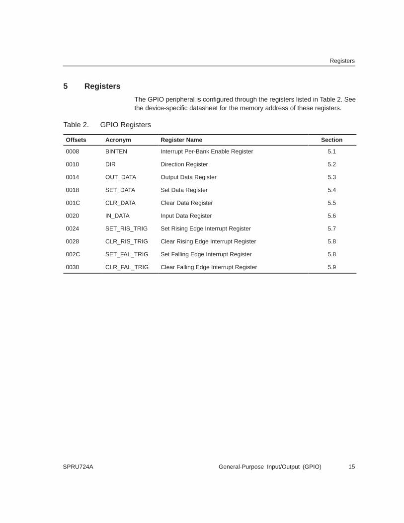
5 Registers
The GPIO peripheral is configured through the registers listed in Table 2. Seethe device-specific datasheet for the memory address of these registers.
Table 2. GPIO Registers
Offsets Acronym Register Name Section
0008 BINTEN Interrupt Per-Bank Enable Register 5.1
0010 DIR Direction Register 5.2
0014 OUT_DATA Output Data Register 5.3
0018 SET_DATA Set Data Register 5.4
001C CLR_DATA Clear Data Register 5.5
0020 IN_DATA Input Data Register 5.6
0024 SET_RIS_TRIG Set Rising Edge Interrupt Register 5.7
0028 CLR_RIS_TRIG Clear Rising Edge Interrupt Register 5.8
002C SET_FAL_TRIG Set Falling Edge Interrupt Register 5.8
0030 CLR_FAL_TRIG Clear Falling Edge Interrupt Register 5.9
Registers
General-Purpose Input/Output (GPIO)16 SPRU724A
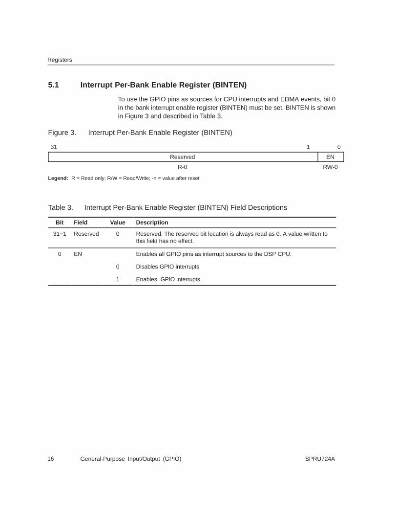
5.1 Interrupt Per-Bank Enable Register (BINTEN)
To use the GPIO pins as sources for CPU interrupts and EDMA events, bit 0in the bank interrupt enable register (BINTEN) must be set. BINTEN is shownin Figure 3 and described in Table 3.
Figure 3. Interrupt Per-Bank Enable Register (BINTEN)
31 1 0
Reserved EN
R-0 RW-0
Legend: R = Read only; R/W = Read/Write; -n = value after reset
Table 3. Interrupt Per-Bank Enable Register (BINTEN) Field Descriptions
Bit Field Value Description
31−1 Reserved 0 Reserved. The reserved bit location is always read as 0. A value written tothis field has no effect.
0 EN Enables all GPIO pins as interrupt sources to the DSP CPU.
0 Disables GPIO interrupts
1 Enables GPIO interrupts

Registers
17General-Purpose Input/Output (GPIO)SPRU724A
5.2 Direction Register (DIR)
The GPIO direction register (DIR) determines if a given GPIO pin is an inputor an output. The GPDIR is shown in Figure 4 and described in Table 4. Bydefault, all the GPIO pins are configured as input pins.
When GPIO pins are configured as output pins, the GPIO output buffer drivesthe GPIO pin. If it is necessary to place the GPIO output buffer in ahigh-impedance state, the GPIO pin must be configured as an input pin(DIRn = 1). At reset, GPIO pins default to input mode.
Figure 4. Direction Register (DIR)
31 16
Reserved
R-0
15 14 13 12 11 10 9 8
DIR15 DIR14 DIR13 DIR12 DIR11 DIR10 DIR9 DIR8
R/W-1 R/W-1 R/W-1 R/W-1 R/W-1 R/W-1 R/W-1 R/W-1
7 6 5 4 3 2 1 0
DIR7 DIR6 DIR5 DIR4 DIR3 DIR2 DIR1 DIR0
R/W-1 R/W-1 R/W-1 R/W-1 R/W-1 R/W-1 R/W-1 R/W-1
Legend: R = Read only; R/W = Read/Write; -n = value after reset
Table 4. Direction Register (DIR) Field Descriptions
Bit Field Value Description
31−16 Reserved 0 Reserved. The reserved bit location is always read as 0. A value written tothis field has no effect.
15−0 DIRn Controls the direction of the GPn pin.
0 GPn pin configured as output pin
1 GPn pin configured as input pin

Registers
General-Purpose Input/Output (GPIO)18 SPRU724A
5.3 Output Data Register (OUT_DATA)
The GPIO output data register (OUT_DATA) indicates the value to be drivenon a given GPIO output pin. The OUT_DATA registers are shown in Figure 5and described in Table 5.
Figure 5. Output Data Register (OUT_DATA)
31 16
Reserved
R-0
15 14 13 12 11 10 9 8
OUT15 OUT14 OUT13 OUT12 OUT11 OUT10 OUT9 OUT8
R/W-0 R/W-0 R/W-0 R/W-0 R/W-0 R/W-0 R/W-0 R/W-0
7 6 5 4 3 2 1 0
OUT7 OUT6 OUT5 OUT4 OUT3 OUT2 OUT1 OUT0
R/W-0 R/W-0 R/W-0 R/W-0 R/W-0 R/W-0 R/W-0 R/W-0
Legend: R = Read only; R/W = Read/Write; -n = value after reset
Table 5. Output Data Register (OUT_DATA) Field Descriptions
Bit Field Value Description
31−16 Reserved 0 Reserved. The reserved bit location is always read as 0. A value written tothis field has no effect.
15−0 OUTn Controls the drive state of the corresponding GPn pin. These bits do notaffect the state of the pin when the pin is configured as an input. Readingthese bits returns the value of this register, not the state of the pin.

Registers
19General-Purpose Input/Output (GPIO)SPRU724A
5.4 Set Data Register (SET_DATA)
The GPIO set data register (SET_DATA) is shown in Figure 6 and describedin Table 6. SET_DATA provides an alternate means of driving GPIO outputshigh. Writing a 1 to a bit of SET_DATA sets the corresponding bit inOUT_DATA. Writing a 0 has no effect. Reading SET_DATA returns thecontents of OUT_DATA.
Figure 6. Set Data Register (SET_DATA)
31 16
Reserved
R-0
15 14 13 12 11 10 9 8
SET15 SET14 SET13 SET12 SET11 SET10 SET9 SET8
R/W-0 R/W-0 R/W-0 R/W-0 R/W-0 R/W-0 R/W-0 R/W-0
7 6 5 4 3 2 1 0
SET7 SET6 SET5 SET4 SET3 SET2 SET1 SET0
R/W-0 R/W-0 R/W-0 R/W-0 R/W-0 R/W-0 R/W-0 R/W-0
Legend: R = Read only; R/W = Read/Write; -n = value after reset
Table 6. Set Data Register (SET_DATA) Field Descriptions
Bit Field Value Description
31−16 Reserved 0 Reserved. The reserved bit location is always read as 0. A value written tothis field has no effect.
15−0 SETn Writing 1 sets the corresponding bit the OUT_DATA register. Reading thisregister returns the contents of the OUT_DATA register. Writing a 0 has noeffect.
0 No effect
1 Sets the corresponding bit in OUT_DATA
Registers
General-Purpose Input/Output (GPIO)20 SPRU724A
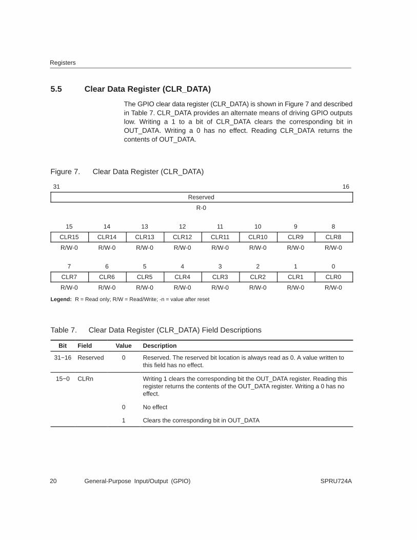
5.5 Clear Data Register (CLR_DATA)
The GPIO clear data register (CLR_DATA) is shown in Figure 7 and describedin Table 7. CLR_DATA provides an alternate means of driving GPIO outputslow. Writing a 1 to a bit of CLR_DATA clears the corresponding bit inOUT_DATA. Writing a 0 has no effect. Reading CLR_DATA returns thecontents of OUT_DATA.
Figure 7. Clear Data Register (CLR_DATA)
31 16
Reserved
R-0
15 14 13 12 11 10 9 8
CLR15 CLR14 CLR13 CLR12 CLR11 CLR10 CLR9 CLR8
R/W-0 R/W-0 R/W-0 R/W-0 R/W-0 R/W-0 R/W-0 R/W-0
7 6 5 4 3 2 1 0
CLR7 CLR6 CLR5 CLR4 CLR3 CLR2 CLR1 CLR0
R/W-0 R/W-0 R/W-0 R/W-0 R/W-0 R/W-0 R/W-0 R/W-0
Legend: R = Read only; R/W = Read/Write; -n = value after reset
Table 7. Clear Data Register (CLR_DATA) Field Descriptions
Bit Field Value Description
31−16 Reserved 0 Reserved. The reserved bit location is always read as 0. A value written tothis field has no effect.
15−0 CLRn Writing 1 clears the corresponding bit the OUT_DATA register. Reading thisregister returns the contents of the OUT_DATA register. Writing a 0 has noeffect.
0 No effect
1 Clears the corresponding bit in OUT_DATA
Registers
21General-Purpose Input/Output (GPIO)SPRU724A
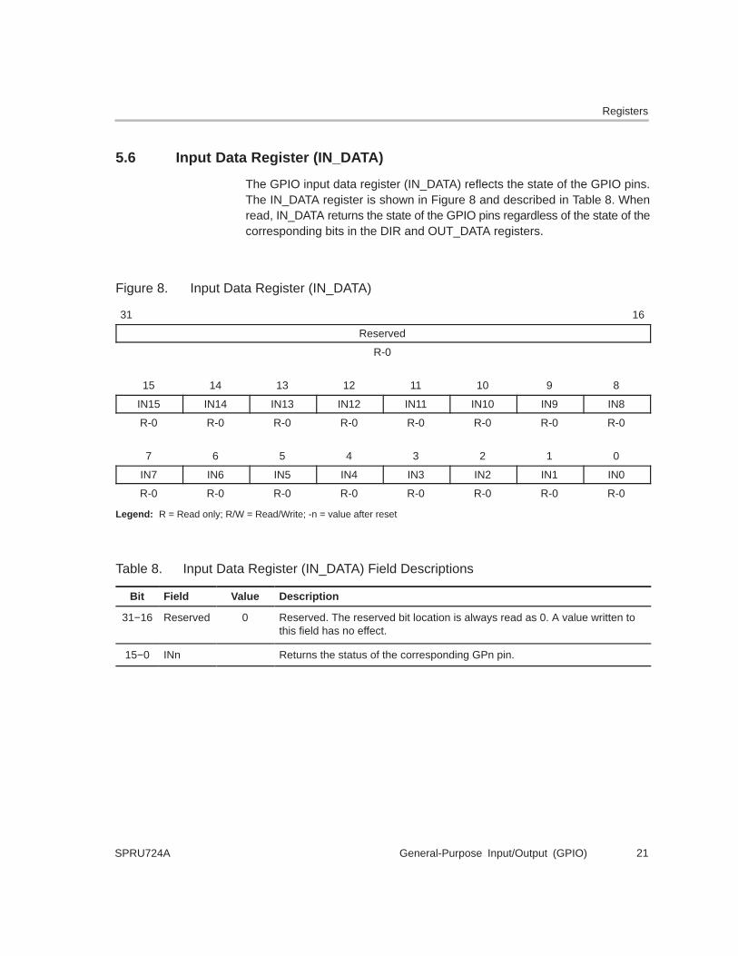
5.6 Input Data Register (IN_DATA)
The GPIO input data register (IN_DATA) reflects the state of the GPIO pins.The IN_DATA register is shown in Figure 8 and described in Table 8. Whenread, IN_DATA returns the state of the GPIO pins regardless of the state of thecorresponding bits in the DIR and OUT_DATA registers.
Figure 8. Input Data Register (IN_DATA)
31 16
Reserved
R-0
15 14 13 12 11 10 9 8
IN15 IN14 IN13 IN12 IN11 IN10 IN9 IN8
R-0 R-0 R-0 R-0 R-0 R-0 R-0 R-0
7 6 5 4 3 2 1 0
IN7 IN6 IN5 IN4 IN3 IN2 IN1 IN0
R-0 R-0 R-0 R-0 R-0 R-0 R-0 R-0
Legend: R = Read only; R/W = Read/Write; -n = value after reset
Table 8. Input Data Register (IN_DATA) Field Descriptions
Bit Field Value Description
31−16 Reserved 0 Reserved. The reserved bit location is always read as 0. A value written tothis field has no effect.
15−0 INn Returns the status of the corresponding GPn pin.
Registers
General-Purpose Input/Output (GPIO)22 SPRU724A
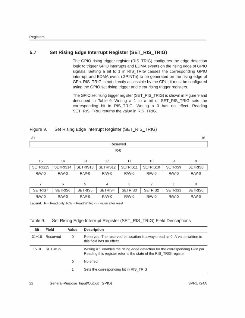
5.7 Set Rising Edge Interrupt Register (SET_RIS_TRIG)
The GPIO rising trigger register (RIS_TRIG) configures the edge detectionlogic to trigger GPIO interrupts and EDMA events on the rising edge of GPIOsignals. Setting a bit to 1 in RIS_TRIG causes the corresponding GPIOinterrupt and EDMA event (GPINTn) to be generated on the rising edge ofGPn. RIS_TRIG is not directly accessible by the CPU; it must be configuredusing the GPIO set rising trigger and clear rising trigger registers.
The GPIO set rising trigger register (SET_RIS_TRIG) is shown in Figure 9 anddescribed in Table 9. Writing a 1 to a bit of SET_RIS_TRIG sets thecorresponding bit in RIS_TRIG. Writing a 0 has no effect. ReadingSET_RIS_TRIG returns the value in RIS_TRIG.
Figure 9. Set Rising Edge Interrupt Register (SET_RIS_TRIG)
31 16
Reserved
R-0
15 14 13 12 11 10 9 8
SETRIS15 SETRIS14 SETRIS13 SETRIS12 SETRIS11 SETRIS10 SETRIS9 SETRIS8
R/W-0 R/W-0 R/W-0 R/W-0 R/W-0 R/W-0 R/W-0 R/W-0
7 6 5 4 3 2 1 0
SETRIS7 SETRIS6 SETRIS5 SETRIS4 SETRIS3 SETRIS2 SETRIS1 SETRIS0
R/W-0 R/W-0 R/W-0 R/W-0 R/W-0 R/W-0 R/W-0 R/W-0
Legend: R = Read only; R/W = Read/Write; -n = value after reset
Table 9. Set Rising Edge Interrupt Register (SET_RIS_TRIG) Field Descriptions
Bit Field Value Description
31−16 Reserved 0 Reserved. The reserved bit location is always read as 0. A value written tothis field has no effect.
15−0 SETRISn Writing a 1 enables the rising edge detection for the corresponding GPn pin.Reading this register returns the state of the RIS_TRIG register.
0 No effect
1 Sets the corresponding bit in RIS_TRIG

Registers
23General-Purpose Input/Output (GPIO)SPRU724A
5.8 Clear Rising Edge Interrupt Register (CLR_RIS_TRIG)
The GPIO rising trigger register (RIS_TRIG) configures the edge detectionlogic to trigger GPIO interrupts and EDMA events on the rising edge of GPIOsignals. Setting a bit to 1 in RIS_TRIG causes the corresponding GPIOinterrupt and EDMA event (GPINTn) to be generated on the rising edge ofGPn. RIS_TRIG is not directly accessible by the CPU; it must be configuredusing the GPIO set rising trigger and clear rising trigger registers.
The GPIO clear rising trigger register (CLR_RIS_TRIG) is shown in Figure 10and described in Table 10. Writing a 1 to a bit of CLR_RIS_TRIG clears thecorresponding bit in RIS_TRIG. Writing a 0 has no effect. ReadingCLR_RIS_TRIG returns the value in RIS_TRIG.
Figure 10. Clear Rising Edge Interrupt Register (CLR_RIS_TRIG)
31 16
Reserved
R-0
15 14 13 12 11 10 9 8
CLRRIS15 CLRRIS14 CLRRIS13 CLRRIS12 CLRRIS11 CLRRIS10 CLRRIS9 CLRRIS8
R/W-0 R/W-0 R/W-0 R/W-0 R/W-0 R/W-0 R/W-0 R/W-0
7 6 5 4 3 2 1 0
CLRRIS7 CLRRIS6 CLRRIS5 CLRRIS4 CLRRIS3 CLRRIS2 CLRRIS1 CLRRIS0
R/W-0 R/W-0 R/W-0 R/W-0 R/W-0 R/W-0 R/W-0 R/W-0
Legend: R = Read only; R/W = Read/Write; -n = value after reset
Table 10. Clear Rising Edge Interrupt Register (CLR_RIS_TRIG) Field Descriptions
Bit Field Value Description
31−16 Reserved 0 Reserved. The reserved bit location is always read as 0. A value written tothis field has no effect.
15−0 CLRRISn Writing a 1 disables rising edge detection for the corresponding GPn pin.Reading this register returns the state of the RIS_TRIG register.
0 No effect
1 Clears the corresponding bit in RIS_TRIG
Registers
General-Purpose Input/Output (GPIO)24 SPRU724A
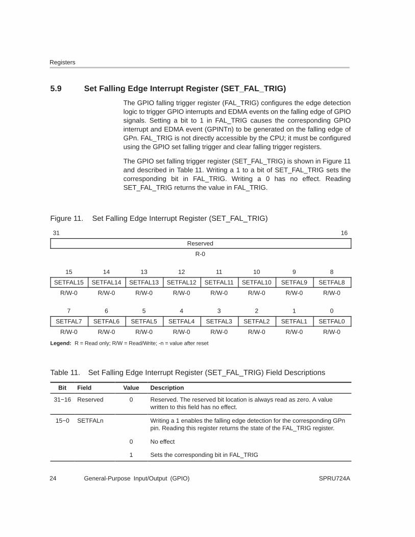
5.9 Set Falling Edge Interrupt Register (SET_FAL_TRIG)
The GPIO falling trigger register (FAL_TRIG) configures the edge detectionlogic to trigger GPIO interrupts and EDMA events on the falling edge of GPIOsignals. Setting a bit to 1 in FAL_TRIG causes the corresponding GPIOinterrupt and EDMA event (GPINTn) to be generated on the falling edge ofGPn. FAL_TRIG is not directly accessible by the CPU; it must be configuredusing the GPIO set falling trigger and clear falling trigger registers.
The GPIO set falling trigger register (SET_FAL_TRIG) is shown in Figure 11and described in Table 11. Writing a 1 to a bit of SET_FAL_TRIG sets thecorresponding bit in FAL_TRIG. Writing a 0 has no effect. ReadingSET_FAL_TRIG returns the value in FAL_TRIG.
Figure 11. Set Falling Edge Interrupt Register (SET_FAL_TRIG)
31 16
Reserved
R-0
15 14 13 12 11 10 9 8
SETFAL15 SETFAL14 SETFAL13 SETFAL12 SETFAL11 SETFAL10 SETFAL9 SETFAL8
R/W-0 R/W-0 R/W-0 R/W-0 R/W-0 R/W-0 R/W-0 R/W-0
7 6 5 4 3 2 1 0
SETFAL7 SETFAL6 SETFAL5 SETFAL4 SETFAL3 SETFAL2 SETFAL1 SETFAL0
R/W-0 R/W-0 R/W-0 R/W-0 R/W-0 R/W-0 R/W-0 R/W-0
Legend: R = Read only; R/W = Read/Write; -n = value after reset
Table 11. Set Falling Edge Interrupt Register (SET_FAL_TRIG) Field Descriptions
Bit Field Value Description
31−16 Reserved 0 Reserved. The reserved bit location is always read as zero. A valuewritten to this field has no effect.
15−0 SETFALn Writing a 1 enables the falling edge detection for the corresponding GPnpin. Reading this register returns the state of the FAL_TRIG register.
0 No effect
1 Sets the corresponding bit in FAL_TRIG
Registers
25General-Purpose Input/Output (GPIO)SPRU724A
5.10 Clear Falling Edge Interrupt Register (CLR_FAL_TRIG)
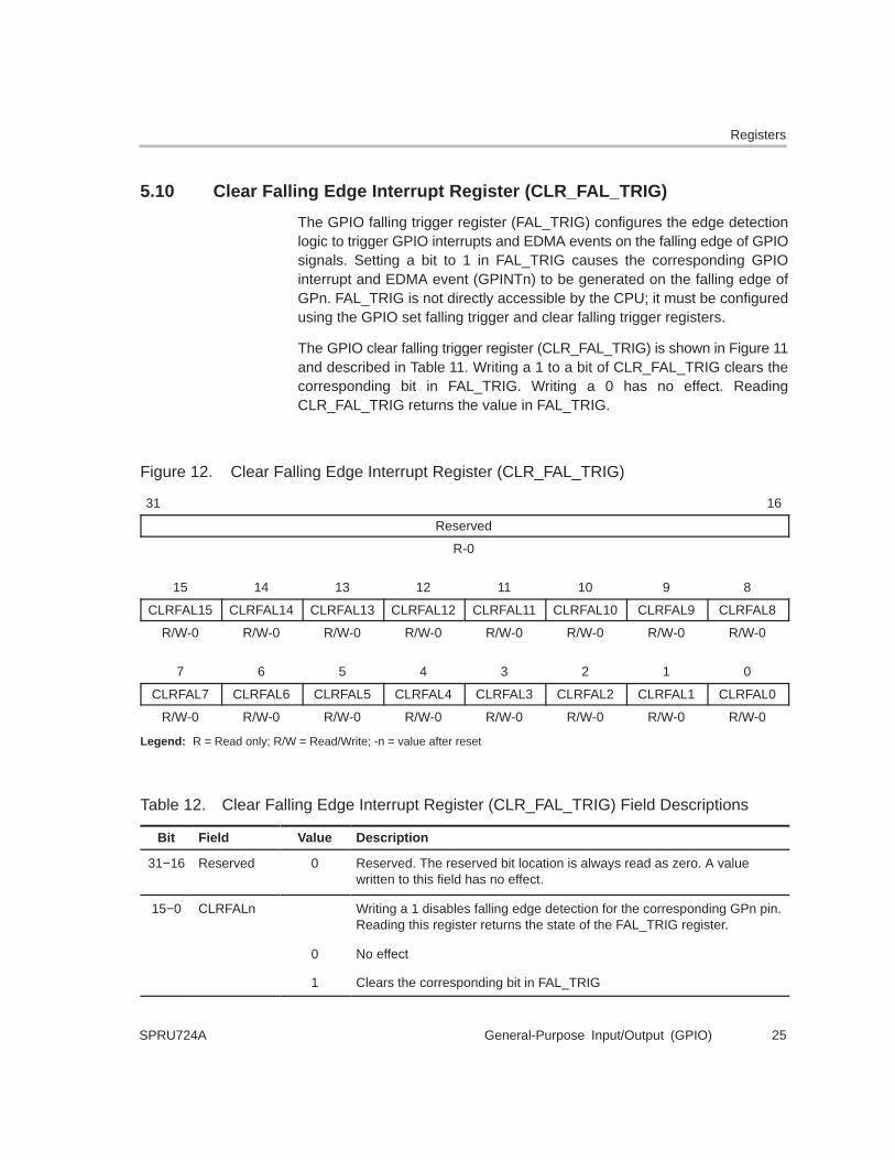
The GPIO falling trigger register (FAL_TRIG) configures the edge detectionlogic to trigger GPIO interrupts and EDMA events on the falling edge of GPIOsignals. Setting a bit to 1 in FAL_TRIG causes the corresponding GPIOinterrupt and EDMA event (GPINTn) to be generated on the falling edge ofGPn. FAL_TRIG is not directly accessible by the CPU; it must be configuredusing the GPIO set falling trigger and clear falling trigger registers.
The GPIO clear falling trigger register (CLR_FAL_TRIG) is shown in Figure 11and described in Table 11. Writing a 1 to a bit of CLR_FAL_TRIG clears thecorresponding bit in FAL_TRIG. Writing a 0 has no effect. ReadingCLR_FAL_TRIG returns the value in FAL_TRIG.
Figure 12. Clear Falling Edge Interrupt Register (CLR_FAL_TRIG)
31 16
Reserved
R-0
15 14 13 12 11 10 9 8
CLRFAL15 CLRFAL14 CLRFAL13 CLRFAL12 CLRFAL11 CLRFAL10 CLRFAL9 CLRFAL8
R/W-0 R/W-0 R/W-0 R/W-0 R/W-0 R/W-0 R/W-0 R/W-0
7 6 5 4 3 2 1 0
CLRFAL7 CLRFAL6 CLRFAL5 CLRFAL4 CLRFAL3 CLRFAL2 CLRFAL1 CLRFAL0
R/W-0 R/W-0 R/W-0 R/W-0 R/W-0 R/W-0 R/W-0 R/W-0
Legend: R = Read only; R/W = Read/Write; -n = value after reset
Table 12. Clear Falling Edge Interrupt Register (CLR_FAL_TRIG) Field Descriptions
Bit Field Value Description
31−16 Reserved 0 Reserved. The reserved bit location is always read as zero. A valuewritten to this field has no effect.
15−0 CLRFALn Writing a 1 disables falling edge detection for the corresponding GPn pin.Reading this register returns the state of the FAL_TRIG register.
0 No effect
1 Clears the corresponding bit in FAL_TRIG

General-Purpose Input/Output (GPIO)26 SPRU724A
This page is intentionally left blank.

Index
27General-Purpose Input/Output (GPIO)SPRU724A
�����
B
block diagramC645x DSP 10GPIO 11
E
event generation 13
events 14
F
function 12
Iinterrupt generation 13interrupts 14
Nnotational conventions 3
Ooverview 9
Rregisters 15related documentation from Texas Instruments 3
Ttrademarks 4

IMPORTANT NOTICETexas Instruments Incorporated and its subsidiaries (TI) reserve the right to make corrections, modifications, enhancements, improvements,and other changes to its products and services at any time and to discontinue any product or service without notice. Customers shouldobtain the latest relevant information before placing orders and should verify that such information is current and complete. All products aresold subject to TI’s terms and conditions of sale supplied at the time of order acknowledgment.TI warrants performance of its hardware products to the specifications applicable at the time of sale in accordance with TI’s standardwarranty. Testing and other quality control techniques are used to the extent TI deems necessary to support this warranty. Except wheremandated by government requirements, testing of all parameters of each product is not necessarily performed.TI assumes no liability for applications assistance or customer product design. Customers are responsible for their products andapplications using TI components. To minimize the risks associated with customer products and applications, customers should provideadequate design and operating safeguards.TI does not warrant or represent that any license, either express or implied, is granted under any TI patent right, copyright, mask work right,or other TI intellectual property right relating to any combination, machine, or process in which TI products or services are used. Informationpublished by TI regarding third-party products or services does not constitute a license from TI to use such products or services or awarranty or endorsement thereof. Use of such information may require a license from a third party under the patents or other intellectualproperty of the third party, or a license from TI under the patents or other intellectual property of TI.Reproduction of TI information in TI data books or data sheets is permissible only if reproduction is without alteration and is accompaniedby all associated warranties, conditions, limitations, and notices. Reproduction of this information with alteration is an unfair and deceptivebusiness practice. TI is not responsible or liable for such altered documentation. Information of third parties may be subject to additionalrestrictions.Resale of TI products or services with statements different from or beyond the parameters stated by TI for that product or service voids allexpress and any implied warranties for the associated TI product or service and is an unfair and deceptive business practice. TI is notresponsible or liable for any such statements.TI products are not authorized for use in safety-critical applications (such as life support) where a failure of the TI product would reasonablybe expected to cause severe personal injury or death, unless officers of the parties have executed an agreement specifically governingsuch use. Buyers represent that they have all necessary expertise in the safety and regulatory ramifications of their applications, andacknowledge and agree that they are solely responsible for all legal, regulatory and safety-related requirements concerning their productsand any use of TI products in such safety-critical applications, notwithstanding any applications-related information or support that may beprovided by TI. Further, Buyers must fully indemnify TI and its representatives against any damages arising out of the use of TI products insuch safety-critical applications.TI products are neither designed nor intended for use in military/aerospace applications or environments unless the TI products arespecifically designated by TI as military-grade or "enhanced plastic." Only products designated by TI as military-grade meet militaryspecifications. Buyers acknowledge and agree that any such use of TI products which TI has not designated as military-grade is solely atthe Buyer's risk, and that they are solely responsible for compliance with all legal and regulatory requirements in connection with such use.TI products are neither designed nor intended for use in automotive applications or environments unless the specific TI products aredesignated by TI as compliant with ISO/TS 16949 requirements. Buyers acknowledge and agree that, if they use any non-designatedproducts in automotive applications, TI will not be responsible for any failure to meet such requirements.Following are URLs where you can obtain information on other Texas Instruments products and application solutions:Products ApplicationsAmplifiers amplifier.ti.com Audio www.ti.com/audioData Converters dataconverter.ti.com Automotive www.ti.com/automotiveDSP dsp.ti.com Broadband www.ti.com/broadbandClocks and Timers www.ti.com/clocks Digital Control www.ti.com/digitalcontrolInterface interface.ti.com Medical www.ti.com/medicalLogic logic.ti.com Military www.ti.com/militaryPower Mgmt power.ti.com Optical Networking www.ti.com/opticalnetworkMicrocontrollers microcontroller.ti.com Security www.ti.com/securityRFID www.ti-rfid.com Telephony www.ti.com/telephonyRF/IF and ZigBee® Solutions www.ti.com/lprf Video & Imaging www.ti.com/video
Wireless www.ti.com/wireless
Mailing Address: Texas Instruments, Post Office Box 655303, Dallas, Texas 75265Copyright © 2008, Texas Instruments Incorporated